MEM’s Computer Aided Design Dr. Lynn Fullerpeople.rit.edu/lffeee/MEMS_CAD.pdf · USING THE HP...
28
© March 31, 2004 Dr. Lynn Fuller, Motorola Professor MEM’s CAD Page 1 Rochester Institute of Technology Microelectronic Engineering ROCHESTER INSTITUTE OF TECHNOLOGY MICROELECTRONIC ENGINEERING 3-31-2004 MEMS_LAB.PPT MEM’s Computer Aided Design Dr. Lynn Fuller Motorola Professor Microelectronic Engineering Rochester Institute of Technology 82 Lomb Memorial Drive Rochester, NY 14623-5604 Tel (585) 475-2035 Fax (585) 475-5041 LFFEEE@rit. edu http://www.microe.rit.edu
Transcript of MEM’s Computer Aided Design Dr. Lynn Fullerpeople.rit.edu/lffeee/MEMS_CAD.pdf · USING THE HP...

© March 31, 2004 Dr. Lynn Fuller, Motorola Professor
MEM’s CAD
Page 1
Rochester Institute of TechnologyMicroelectronic Engineering
ROCHESTER INSTITUTE OF TECHNOLOGYMICROELECTRONIC ENGINEERING
3-31-2004 MEMS_LAB.PPT
MEM’s Computer Aided Design Dr. Lynn Fuller
Motorola Professor Microelectronic Engineering
Rochester Institute of Technology 82 Lomb Memorial Drive Rochester, NY 14623-5604 Tel (585) 475-2035 Fax (585) 475-5041 [email protected]
http://www.microe.rit.edu

© March 31, 2004 Dr. Lynn Fuller, Motorola Professor
MEM’s CAD
Page 2
Rochester Institute of TechnologyMicroelectronic Engineering
RIT MEMS DESIGN RULES
Microelectromechanical SystemsThe basic unit of distance in a scalable set of design rules is called
Lambda, λFor the current MEMS process λ is five microns (5 µm)The process has six mask layers (plus some special layers), they are:
Poly 1 Green (Layer 1)Via Holes Yellow (Layer 5)Anchor Red (Layer 2)Dimple Pink (Layer 50)Poly 2 Grey (Layer 3)Hub Red Outline (Layer 102)Pin Blue (Layer 4)
The following rules are shown as top views(looking down on the mask layers)

© March 31, 2004 Dr. Lynn Fuller, Motorola Professor
MEM’s CAD
Page 3
Rochester Institute of TechnologyMicroelectronic Engineering
DESIGN RULES
Minimum pad size for probing 100 µm by 100 µmMinimum pad size for wire connections 1000 µm by 1000 µmAll probe pads have metal top layer.
10 µm by 10 µm box needed in four corners of 4000 µm by4000 µm work space. (for maskmaking accuracy)
Include etch holes when making patterns for large areapoly-two regions for which the sacrificial oxide is to beremoved.

© March 31, 2004 Dr. Lynn Fuller, Motorola Professor
MEM’s CAD
Page 4
Rochester Institute of TechnologyMicroelectronic Engineering
LAYOUT RULES
Perfect Overlay Slight OverlayNot Fatal
MisalignmentFatal
Layout rules prevent slight misalignment from being fatal.Also, rules help make device performance consistent (minimumwidth for resistor will make values more consistent)

© March 31, 2004 Dr. Lynn Fuller, Motorola Professor
MEM’s CAD
Page 5
Rochester Institute of TechnologyMicroelectronic Engineering
RULES FOR THE POLY ONE LEVEL
10 by 10 µm
Layer 1 - Poly 1 (green)
Rule 1.1 Minimum Width Wz = 4 λ
Rule 1.2 Minimum SpacingSzz = 2 λ
Wz = 4 λ (20 µm)
Szz = 2 λ (10 µm)
© March 31, 2004 Dr. Lynn Fuller, Motorola Professor
MEM’s CAD
Page 6
Rochester Institute of TechnologyMicroelectronic Engineering
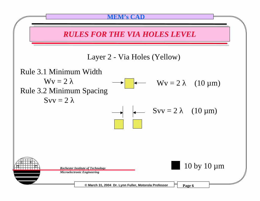
RULES FOR THE VIA HOLES LEVEL
10 by 10 µm
Layer 2 - Via Holes (Yellow)
Rule 3.1 Minimum Width Wv = 2 λ
Rule 3.2 Minimum SpacingSvv = 2 λ
Wv = 2 λ (10 µm)
Svv = 2 λ (10 µm)

© March 31, 2004 Dr. Lynn Fuller, Motorola Professor
MEM’s CAD
Page 7
Rochester Institute of TechnologyMicroelectronic Engineering
RULES FOR THE ANCHOR LEVEL
10 by 10 µm
Layer 3 - Anchor (Red)
Rule 2.1 Minimum Width Wa = 4 λ
Rule 2.2 Minimum SpacingSaa = 2 λ
Wmin = 4 λ (20 µm)
Smin = 2λ (10 µm)

© March 31, 2004 Dr. Lynn Fuller, Motorola Professor
MEM’s CAD
Page 8
Rochester Institute of TechnologyMicroelectronic Engineering
RULES FOR DIMPLE LEVEL
10 by 10 µm
Layer 4 - Dimple (Pink)
Rule 3.1 Minimum Width Wd= 2 λ
Rule 3.2 Minimum SpacingSdd = 2 λ
Wd = 2 λ (10 µm)
Sdd = 4 λ (20 µm)

© March 31, 2004 Dr. Lynn Fuller, Motorola Professor
MEM’s CAD
Page 9
Rochester Institute of TechnologyMicroelectronic Engineering
RULES FOR POLY TWO LEVEL
10 by 10 µm
Layer 5 - Poly Two (Grey)Rule 4.1 Minimum Width
Wp = 4 λRule 4.2 Minimum Spacing
Spp = λWp = 4 λ (20 µm)
Spp = λ (5 µm)Spg = 2 µm
Anchor
Comb Drive GapSpg = 2 µm

© March 31, 2004 Dr. Lynn Fuller, Motorola Professor
MEM’s CAD
Page 10
Rochester Institute of TechnologyMicroelectronic Engineering
RULES FOR THE POLY ONE, ANCHOR AND POLY TWO TOGETHER
Layer 1,2,3 Overlay (Extension)
Rule 1.3 Minimum Extension of poly one beyond anchor
Eza = 2 λRule 2.3 Minimum Extension of poly two beyond Anchor
Epa = 2 λRule 2.4 Minimum Extension of poly two beyond Dimple
Epd = 1 λ
(10 µm)
(10 µm)Epa
Epd
© March 31, 2004 Dr. Lynn Fuller, Motorola Professor
MEM’s CAD
Page 11
Rochester Institute of TechnologyMicroelectronic Engineering
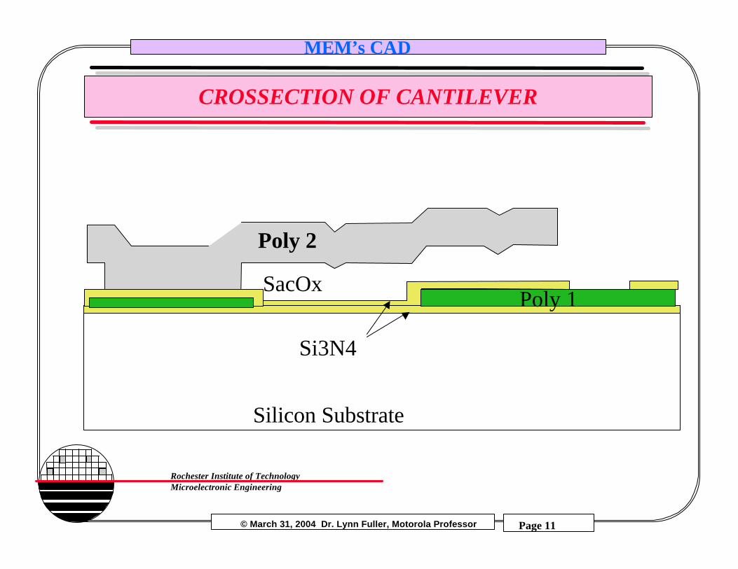
CROSSECTION OF CANTILEVER
Poly 1
Poly 2
SacOx
Silicon Substrate
Si3N4

© March 31, 2004 Dr. Lynn Fuller, Motorola Professor
MEM’s CAD
Page 12
Rochester Institute of TechnologyMicroelectronic Engineering
CROSSECTION OF GEAR
SacOx
Silicon Substrate
Si3N4
Poly 2Poly 2Poly 2
Poly 3

© March 31, 2004 Dr. Lynn Fuller, Motorola Professor
MEM’s CAD
Page 13
Rochester Institute of TechnologyMicroelectronic Engineering
SIMPLIFIED PROCESS SEQUENCE
LPCVD Nitride OneLPCVD Poly One (0.5 µm)Dope PolyPhotlithography Poly OneEtch Poly OneLPCVD Nitride TwoPhotolithography ViaEtch ViaLPCVD Sac Ox (2.0 µm)Photolithography AnchorEtch AnchorPhotolithography DimpleLPCVD Poly Two (2 µm)Dope Poly TwoDeposit Aluminum Etch MaskPhotolithography Poly TwoEtch Poly TwoRelease by Etching Sac Ox
Poly 1
Poly 2
SacOx
Silicon Substrate
Si3N4

© March 31, 2004 Dr. Lynn Fuller, Motorola Professor
MEM’s CAD
Page 14
Rochester Institute of TechnologyMicroelectronic Engineering
LAYOUT OF A CANTILEVER

© March 31, 2004 Dr. Lynn Fuller, Motorola Professor
MEM’s CAD
Page 15
Rochester Institute of TechnologyMicroelectronic Engineering
LAYOUT OF A ELECTROSTATIC COMB DRIVE
Anchor
Comb Drive GapSpg = 2 µm

© March 31, 2004 Dr. Lynn Fuller, Motorola Professor
MEM’s CAD
Page 16
Rochester Institute of TechnologyMicroelectronic Engineering
MEMS MULTI-PROJECT CHIP
4mm by 4mmDesign Spacefor Each Project
Total 16 mm by16 mm for 16student projects

© March 31, 2004 Dr. Lynn Fuller, Motorola Professor
MEM’s CAD
Page 17
Rochester Institute of TechnologyMicroelectronic Engineering
SPRING 1997-98
CantileversSpringsAccelerometerPressure SensorsElectrostatic MotorMirrorsDiffraction GratingGearsPin JointsSliderMicrophone

© March 31, 2004 Dr. Lynn Fuller, Motorola Professor
MEM’s CAD
Page 18
Rochester Institute of TechnologyMicroelectronic Engineering
GCA, Canon, Karl Suss and ASMLAlignment, Resolution and Overlay Structures
Filename/tools/ritpub/alignment-marks/canon.gds or canon.iccel_1
/tools/ritpub/alignment-marks/gca.gds or gca.iccel_1
/tools/ritpub/resolution-overlay/canon.gds or canon.iccel_1
/tools/ritpub/resolution-overlay/canon.gds or canon.iccel_1
60 µm
35 µm45 µm
60 µm
5 µm
600µm
20µm
50 µm
170 µm
150 µm
y-directionMeasurement
x-directionMeasurement
Type20P-4F W=6µm
B=40µm
B
W
A=60µm
A
C=100µm
C
TYPE 0
2.0
1.5
1.0
2.0
1.5
1.0
100µm
10µm

© March 31, 2004 Dr. Lynn Fuller, Motorola Professor
MEM’s CAD
Page 19
Rochester Institute of TechnologyMicroelectronic Engineering
USING THE HP WORKSTATIONS AND MENTORGRAPHICS CAD TOOLS - GETTING STARTED
Usually the workstation screen will be blank, press any key to view a login window.Login: -------- Password: --------
The screen background will change and the control panel will appear. Click the left mousebutton on the terminal icon. A window will appear that says hp term on the top and has a unixprompt inside. Type the command ls at the prompt to see a list of directories and files, theaccount should be empty. Typing yppasswd will allow you to change your password if youwant to.
Type ic <RET>, it will take 20-30 seconds, then maximize the IC Station window by clickingthe left mouse button on the large square in the upper right corner of the IC Station window.

© March 31, 2004 Dr. Lynn Fuller, Motorola Professor
MEM’s CAD
Page 20
Rochester Institute of TechnologyMicroelectronic Engineering
USING THE HP WORKSTATIONS AND MENTORGRAPHICS CAD TOOLS - PROCESS AND GRID
In the session menu palette on the right hand side of the screen, under Cell, select Create,using the lift mouse button. For cell name type device# (the # assigned to you, no space).Also set the process to the RITPMOS process by typing /ritpub/process/ritpmos in the processfield and click on return OK. In the gray area under the banner at the top of the screen, theprocess should now read RITPMOS. Select other>show layer palette, click/drag on layers 1 to4 then press select. Layers colors and shading should appear in upper right corner.
A large window with a black background and white dots should appear. We can now checkthe grid settings. In the top banner choose Other > Window > Set Grid. Set the Snap to 10 forboth x and y, minor=1, major=10, then click on OK
The cursor position is given at the top center of the window. The layer being used and thenumber of items selected is shown at the top right. The 12 gray buttons which correspond tothe F1-F8 and 4 white buttons allow multiple functions. For example push F2 to (UnselectAll). To get the next function listed below that (Unselect Area) push shift and F2. To get thefunction listed on the bottom for the F2 key (Move) press the CTRL key and the F2 key.

© March 31, 2004 Dr. Lynn Fuller, Motorola Professor
MEM’s CAD
Page 21
Rochester Institute of TechnologyMicroelectronic Engineering
USING THE HP WORKSTATIONS AND MENTORGRAPHICS CAD TOOLS - PAD CELL AND LETTERS
From the banner at the top of the page choose Objects>add>cell. A tan pop-up window willappear at the bottom of the page. Type in the following cell name, all lower case,/ritpub/padframes/ritpmos/ritpmos_12_pads and click the left mouse button on the locationbutton. Then position the cursor at the origin 0,0 and click the left mouse button. Click theleft mouse button on the cancel button on the tan pop-up box. Press SHIFT and F8 to ViewAll. You should see a white box with ritpmos_12_pads written inside it. Type flatten andselect, OK. Press F2 to unselect all.
500 µm
100 µm
100 µm
Design Space
ABCDEFGHIJKLMNOPQRSTUVWXYZ00.;:=*/-+1234567890NPN PNP µMVDD VSS GNDSUB +V -V
Note: To get larger letters changethe scale to 4 when bringing in12pads before flattening. Thenflatten. Select and discard theenlarged pads and corner squares.

© March 31, 2004 Dr. Lynn Fuller, Motorola Professor
MEM’s CAD
Page 22
Rochester Institute of TechnologyMicroelectronic Engineering
USING THE HP WORKSTATIONS AND MENTORGRAPHICS CAD TOOLS - DRAWING
Select easy edit, Select Shape, Select Options and see the layer names, colors and shadingpattern. Draw boxes by click and drag of mouse. Unselect by pressing F2 function key.The Notch command is useful to change the size of a selected box or merge rectangularshapes into more complex objects. The following command will draw a 3000 µm by 3000µm box with level 5 color/shading. $add_shape([[0,0],[3000,3000]],5)
Draw circles by typing $set_location_mode(@arc) return. The following command willdraw a 100µm radius circle centered at (0,0) using 300 straight line segments.To reset to rectangles type $set_location_mode(@line) return.
Select objects by clicking or by click and drag. Selected objects will appear to have a brightoutline. Selected objects can be moved (Move), copied (Copy), deleted (Del) or notched(Notc). To unselect objects press F2.

© March 31, 2004 Dr. Lynn Fuller, Motorola Professor
MEM’s CAD
Page 23
Rochester Institute of TechnologyMicroelectronic Engineering
USING THE HP WORKSTATIONS AND MENTORGRAPHICS CAD TOOLS - OTHER
ZOOM IN OUT: pressing the + or - sign on right key pad will zoom in or out. Alsopressing shift + F8 will zoom so that all objects are in the view area. Select View and Areaon top banner then click and drag a rectangle will zoom so that the objects in the rectangleare in the view area.
MOVING VIEW CENTER: pressing the middle mouse button will center the viewaround the pointer.
LASER PRINT OUTPUT: Select File and Print, OK. This gives a laser printer output ofentire cell. Select printer mgcprec2, clear width, len, pages, scale by using backspace sonothing is in those boxes. Say OK.
PRINT PART OF LAYOUT: first create a panel. Under objects, select add a panel, nameit and click on rectangle symbol. Then use the left mouse button to drag a rectangle aroundthe objects you want in the panel to be printed. Then select File and Print and enter panelname, click on print set up, printer is mgcprec2, clear width, len, pages, scale by usingbackspace so nothing is in those boxes. Say OK.

© March 31, 2004 Dr. Lynn Fuller, Motorola Professor
MEM’s CAD
Page 24
Rochester Institute of TechnologyMicroelectronic Engineering
USING THE HP WORKSTATIONS AND MENTORGRAPHICS CAD TOOLS - OTHER
ADDING TEXT: From the banner at the top of the page choose Objects>add>cell. A tanpop-up window will appear at the bottom of the page. Type in the following cell name, alllower case, /tools/ritpub/padframes/ritpmos/ritpmos_12_pads and click the left mousebutton on the location button. Then position the cursor at the origin 0,0 and click the leftmouse button. Click the left mouse button on the cancel button on the tan pop-up box.Press SHIFT and F8 to View All. You should see a white box with ritpmos_12_padswritten inside it. Type flatten and select, OK. Press F2 to unselect all. Use select and copyto place letters you want. To change letters to a different layer use select and set layers.Don’t forget to delete the extra letters and numbers you don’t want.To change text size: Import the cell (F5) with scale option greater than 1 to increase thesize. Try 3 to make letters 100 um high.
orType $add_device(“$pgtext”), select layer and justification and type text, click OK,Type flatten, OKTo change text size, do the text as a separate cell. Import the cell (F5) with scale optiongreater than 1 to increase the size.
© March 31, 2004 Dr. Lynn Fuller, Motorola Professor
MEM’s CAD
Page 25
Rochester Institute of TechnologyMicroelectronic Engineering
USING THE HP WORKSTATIONS AND MENTORGRAPHICS CAD TOOLS - OTHER
COPY A CELL FROM A STUDENTS ACCOUNT TO ANOTHER ACCOUNT: Tocopy from one students account to another account first have a dropbox set up to receive thefile. (for example Dr. Fullers dropbox is /lffeee )
Once the file is saved exit ic.In the terminal window type dmgr_ic, find the design in the right panel of design managerclick on the icon, right click>edit>copy and type the destination ie: /dropbox/lffeee OK
Exit design manager and open a new terminal window. Change directory to the destinationby typing cd /dropbox/lffeee check to see that your files are there by typing ls (4 or 5 files)set the protection to allow the file to be read by typing /usr/bin/chmod 644
and /usr/bin/chmod 644 filename.*
Then the owner of the dropbox can read the files and add the cells to his design. By pressingF5 and typing /dropbox/lffeee/filename, and flatten.
© March 31, 2004 Dr. Lynn Fuller, Motorola Professor
MEM’s CAD
Page 26
Rochester Institute of TechnologyMicroelectronic Engineering
USING THE HP WORKSTATIONS AND MENTORGRAPHICS CAD TOOLS - OTHER
GRAB A PLOT IN TIFF FORMAT TO PUT IN POWERPOINT, ETC.: Open asecond unix window while viewing the chip layout (or any other display) in anotherwindow. Type xv, select option to grab and set pause to ~5 seconds, save to hp account as.tiff file. You will have ~5 seconds to bring up what you want to grab. Log on to hp accountfrom your pc and use FTP software to copy the file to your pc.
SETTING CELL ORIGIN: under CONTEXT
© March 31, 2004 Dr. Lynn Fuller, Motorola Professor
MEM’s CAD
Page 27
Rochester Institute of TechnologyMicroelectronic Engineering
REFERENCES
1. Principles of CMOS VLSI Design, 2nd Ed., Neil H.E.Weste,Kmran Eshraghian, Addison Wesley, 1993.2. Physical Design Automation of VLSI Systems, Bryan Preas,Michael Lorenzeti, Benjamin/Cummings, 1988.3. VLSI Engineering, Thomas Dillinger, Prentice Hall, 1988.

© March 31, 2004 Dr. Lynn Fuller, Motorola Professor
MEM’s CAD
Page 28
Rochester Institute of TechnologyMicroelectronic Engineering
REVIEW QUESTIONS
• Why is the poly two bigger than the anchor?• Why is poly one under the anchor?• Sketch the layout of a torsional mirror that can tip in two
directions.• Sketch the layout of a polysilicon inductor using the first 4
masks in this process.