
Memory Hierarchy Reducing Hit Time Main Memory...
47
Memory Hierarchy Reducing Hit Time Main Memory and Examples Soner Onder Michigan Technological University Randy Katz & David A. Patterson University of California, Berkeley
Transcript of Memory Hierarchy Reducing Hit Time Main Memory...
Memory HierarchyReducing Hit Time
Main Memory and
Examples
Soner Onder
Michigan Technological University
Randy Katz & David A. Patterson
University of California, Berkeley

2
Review: Reducing Misses
3 Cs: Compulsory, Capacity, Conflict1. Reduce Misses via Larger Block Size2. Reduce Misses via Higher Associativity3. Reducing Misses via Victim Cache4. Reducing Misses via Pseudo-Associativity5. Reducing Misses by HW Prefetching Instr, Data6. Reducing Misses by SW Prefetching Data7. Reducing Misses by Compiler Optimizations
Remember danger of concentrating on just one parameter when evaluating performance
CPUtime IC CPIExecution Memory accesses
InstructionMiss rate Miss penalty
Clock cycle time

3
Reducing Miss Penalty Summary
Five techniques Read priority over write on miss Subblock placement Early Restart and Critical Word First on miss Non-blocking Caches (Hit under Miss, Miss under Miss) Second Level Cache
Can be applied recursively to Multilevel Caches Danger is that time to DRAM will grow with multiple levels in between First attempts at L2 caches can make things worse, since increased
worst case is worse
Out-of-order CPU can hide L1 data cache miss (3–5 clocks), but stall on L2 miss (40–100 clocks)?
CPUtime IC CPIExecution Memory accesses
InstructionMiss rate Miss penalty
Clock cycle time
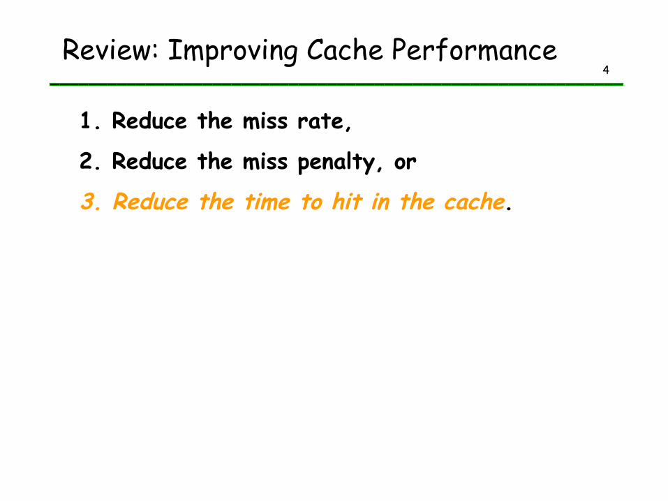
4Review: Improving Cache Performance
1. Reduce the miss rate,
2. Reduce the miss penalty, or
3. Reduce the time to hit in the cache.

5
1. Fast Hit times via Small and Simple Caches
Why Alpha 21164 has 8KB Instruction and 8KB data cache + 96KB second level cache?
Small data cache and clock rate
Direct Mapped, on chip
6
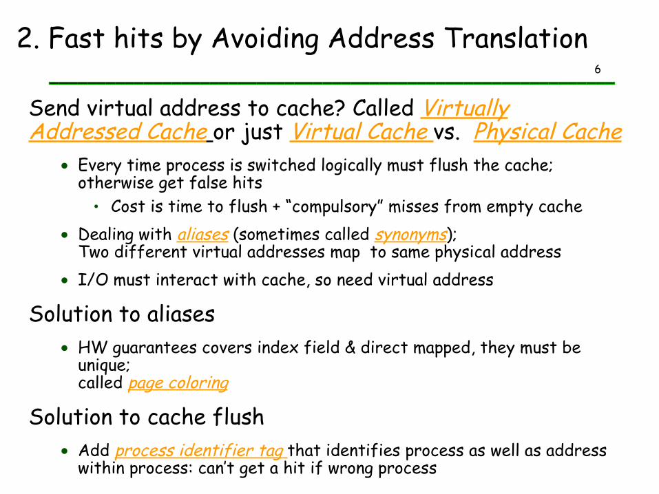
2. Fast hits by Avoiding Address Translation
Send virtual address to cache? Called Virtually Addressed Cache or just Virtual Cache vs. Physical Cache
Every time process is switched logically must flush the cache; otherwise get false hits
Cost is time to flush + “compulsory” misses from empty cache Dealing with aliases (sometimes called synonyms);
Two different virtual addresses map to same physical address I/O must interact with cache, so need virtual address
Solution to aliases HW guarantees covers index field & direct mapped, they must be
unique;called page coloring
Solution to cache flush Add process identifier tag that identifies process as well as address
within process: can’t get a hit if wrong process
7
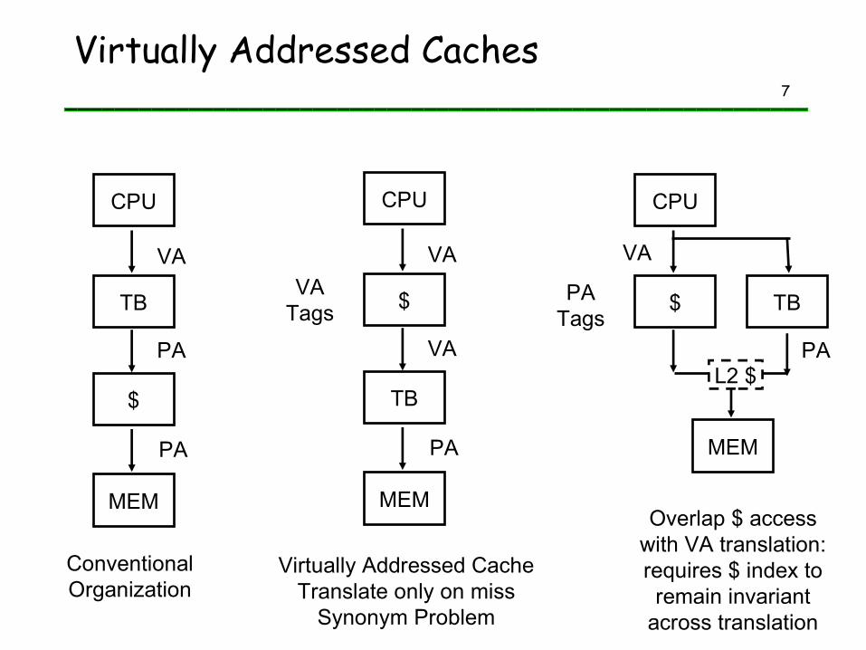
Virtually Addressed Caches
CPU
TB
$
MEM
VA
PA
PA
ConventionalOrganization
CPU
$
TB
MEM
VA
VA
PA
Virtually Addressed CacheTranslate only on miss
Synonym Problem
CPU
$ TB
MEM
VA
PATags
PA
Overlap $ accesswith VA translation:requires $ index to
remain invariantacross translation
VATags
L2 $

8
2. Fast Cache Hits by Avoiding Translation: Process ID impact
Black is uniprocess
Light Gray is multiprocess when flush cache
Dark Gray is multiprocess when use Process ID tag
Y axis: Miss Rates up to 20%
X axis: Cache size from 2 KB to 1024 KB

9
2. Fast Cache Hits by Avoiding Translation: Index with Physical Portion of Address
If index is physical part of address, can start tag access in parallel with translation so that can compare to physical tag
Limits cache to page size: what if want bigger caches and uses same trick?
Higher associativity moves barrier to right Page coloring
Page Address Page Offset
Address Tag Index Block Offset
10
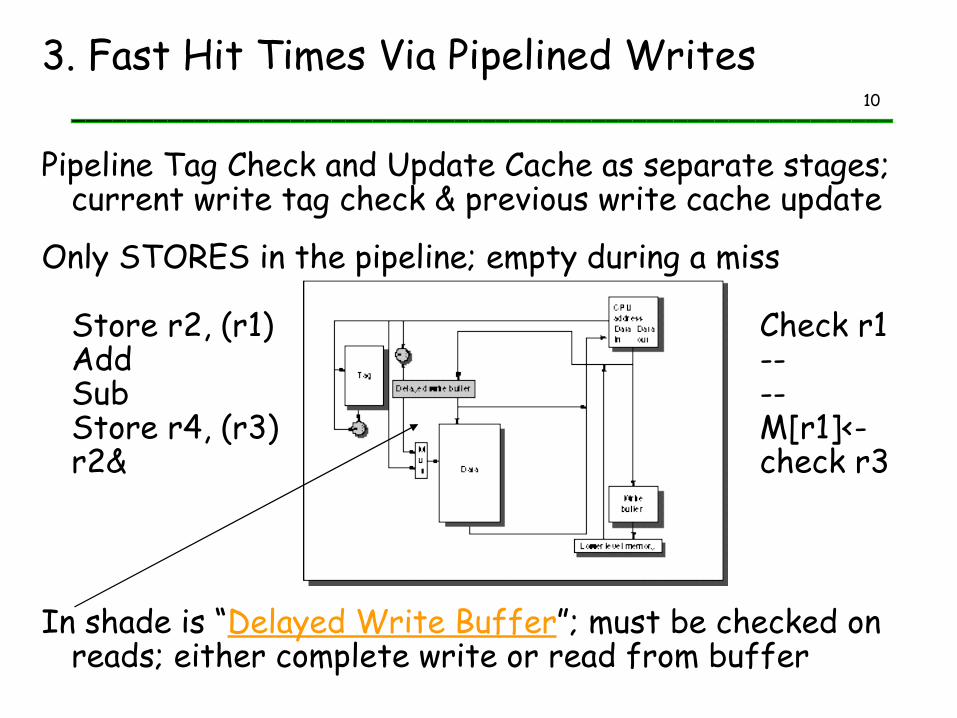
Pipeline Tag Check and Update Cache as separate stages; current write tag check & previous write cache update
Only STORES in the pipeline; empty during a miss
Store r2, (r1) Check r1Add --Sub --Store r4, (r3) M[r1]<-r2& check r3
In shade is “Delayed Write Buffer”; must be checked on reads; either complete write or read from buffer
3. Fast Hit Times Via Pipelined Writes
11
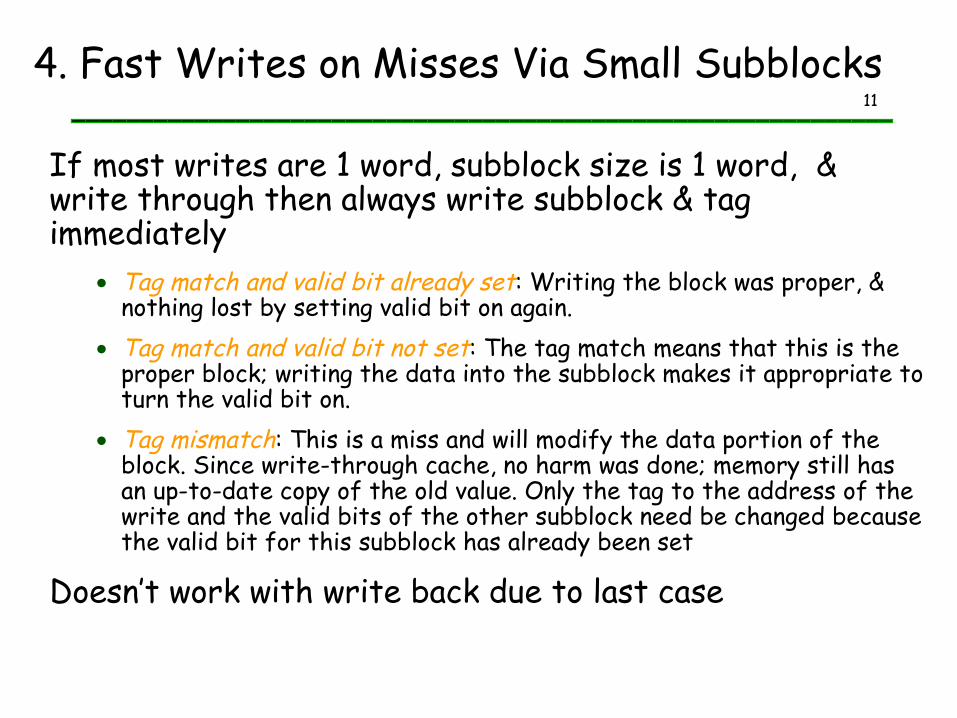
4. Fast Writes on Misses Via Small Subblocks
If most writes are 1 word, subblock size is 1 word, & write through then always write subblock & tag immediately
Tag match and valid bit already set: Writing the block was proper, & nothing lost by setting valid bit on again.
Tag match and valid bit not set: The tag match means that this is the proper block; writing the data into the subblock makes it appropriate to turn the valid bit on.
Tag mismatch: This is a miss and will modify the data portion of the block. Since write-through cache, no harm was done; memory still has an up-to-date copy of the old value. Only the tag to the address of the write and the valid bits of the other subblock need be changed because the valid bit for this subblock has already been set
Doesn’t work with write back due to last case

12
Cache Optimization Summary
Technique MR MP HT Complexity
Larger Block Size + – 0Higher Associativity + – 1Victim Caches + 2Pseudo-Associative Caches + 2HW Prefetching of Instr/Data + 2Compiler Controlled Prefetching + 3Compiler Reduce Misses + 0
Priority to Read Misses + 1Subblock Placement + + 1Early Restart & Critical Word 1st + 2Non-Blocking Caches + 3Second Level Caches + 2
Small & Simple Caches – + 0Avoiding Address Translation + 2Pipelining Writes + 1
mis
s ra
teh
it t
ime
mis
sp
en
alty
13
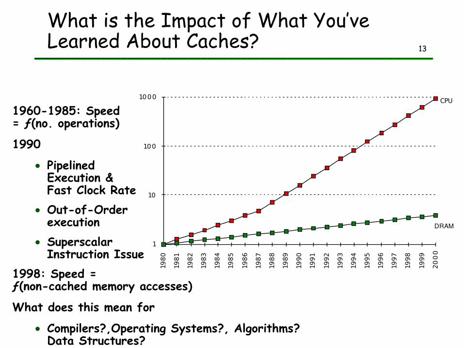
What is the Impact of What You’ve Learned About Caches?
1960-1985: Speed = ƒ(no. operations)
1990
Pipelined Execution & Fast Clock Rate
Out-of-Order execution
Superscalar Instruction Issue
1998: Speed = ƒ(non-cached memory accesses)
What does this mean for
Compilers?,Operating Systems?, Algorithms? Data Structures?
1
10
100
1000
198
0
198
1
198
2
198
3
198
4
198
5
198
6
198
7
198
8
198
9
199
0
199
1
199
2
199
3
199
4
199
5
199
6
199
7
199
8
199
9
20
00
DRAM
CPU

14Main Memory Background
Performance of Main Memory: Latency: Cache Miss Penalty
Access Time: time between request and word arrives Cycle Time: time between requests
Bandwidth: I/O & Large Block Miss Penalty (L2)
Main Memory is DRAM: Dynamic Random Access Memory Dynamic since needs to be refreshed periodically (8 ms, 1% time) Addresses divided into 2 halves (Memory as a 2D matrix):
RAS or Row Access Strobe CAS or Column Access Strobe
Cache uses SRAM: Static Random Access Memory No refresh (6 transistors/bit vs. 1 transistorSize: DRAM/SRAM 4-8,
Cost/Cycle time: SRAM/DRAM 8-16
15
Main Memory Deep Background
“Out-of-Core”, “In-Core,” “Core Dump”?
“Core memory”?
Non-volatile, magnetic
Lost to 4 Kbit DRAM (today using 64Kbit DRAM)
Access time 750 ns, cycle time 1500-3000 ns
16
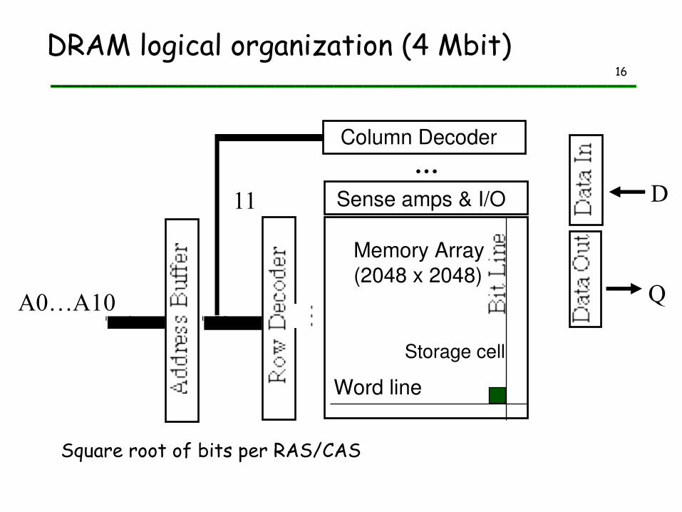
DRAM logical organization (4 Mbit)
Square root of bits per RAS/CAS
Column Decoder
Sense amps & I/O
Memory Array(2048 x 2048)
A0…A10
…
11 D
Q
Word line
Storage cell

17DRAM physical organization (4 Mbit)
Block Row Dec.
9 : 512
RowBlock
Row Dec.9 : 512
Column Address
… BlockRow Dec.
9 : 512
BlockRow Dec.
9 : 512
…
Block 0 Block 3…
I/OI/O
I/OI/O
I/OI/O
I/OI/O
D
Q
Address
2
8 I/Os
8 I/Os
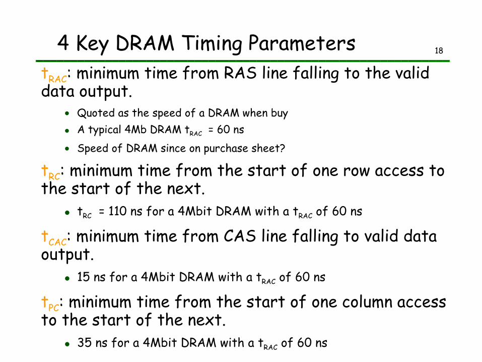
184 Key DRAM Timing ParameterstRAC: minimum time from RAS line falling to the valid data output.
Quoted as the speed of a DRAM when buy A typical 4Mb DRAM tRAC = 60 ns Speed of DRAM since on purchase sheet?
tRC: minimum time from the start of one row access to the start of the next.
tRC = 110 ns for a 4Mbit DRAM with a tRAC of 60 ns
tCAC: minimum time from CAS line falling to valid data output.
15 ns for a 4Mbit DRAM with a tRAC of 60 ns
tPC: minimum time from the start of one column access to the start of the next.
35 ns for a 4Mbit DRAM with a tRAC of 60 ns
19
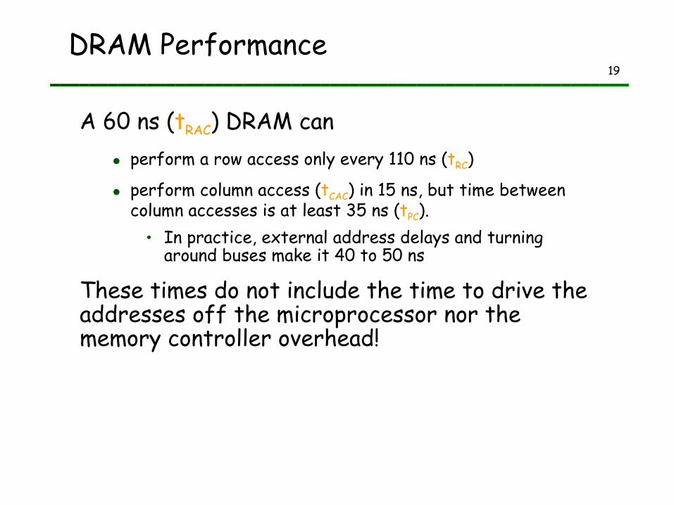
DRAM Performance
A 60 ns (tRAC) DRAM can perform a row access only every 110 ns (tRC)
perform column access (tCAC) in 15 ns, but time between column accesses is at least 35 ns (tPC).
In practice, external address delays and turning around buses make it 40 to 50 ns
These times do not include the time to drive the addresses off the microprocessor nor the memory controller overhead!
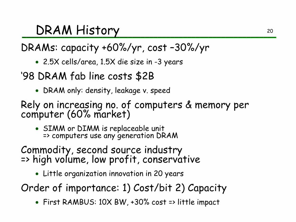
20DRAM HistoryDRAMs: capacity +60%/yr, cost –30%/yr
2.5X cells/area, 1.5X die size in 3 years
‘98 DRAM fab line costs $2B DRAM only: density, leakage v. speed
Rely on increasing no. of computers & memory per computer (60% market)
SIMM or DIMM is replaceable unit => computers use any generation DRAM
Commodity, second source industry => high volume, low profit, conservative
Little organization innovation in 20 years
Order of importance: 1) Cost/bit 2) Capacity First RAMBUS: 10X BW, +30% cost => little impact

21
DRAM Future: 1 Gbit DRAM (ISSCC ‘96; production ‘02?)
Mitsubishi SamsungBlocks 512 x 2 Mbit 1024 x 1 MbitClock 200 MHz 250 MHzData Pins 64 16Die Size 24 x 24 mm 31 x 21 mm
Sizes will be much smaller in production
Metal Layers 3 4Technology 0.15 micron 0.16 micron
Wish could do this for Microprocessors!

22
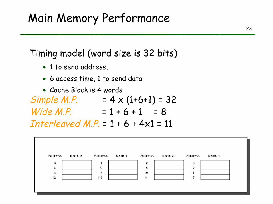
Main Memory Performance
Simple: CPU, Cache, Bus, Memory
same width (32 or 64 bits)
Wide: CPU/Mux 1 word;
Mux/Cache, Bus, Memory N words (Alpha: 64 bits & 256 bits; UtraSPARC 512)
Interleaved: CPU, Cache, Bus 1 word:
Memory N Modules(4 Modules); example is word interleaved
23
Main Memory Performance
Timing model (word size is 32 bits) 1 to send address, 6 access time, 1 to send data Cache Block is 4 words
Simple M.P. = 4 x (1+6+1) = 32Wide M.P. = 1 + 6 + 1 = 8Interleaved M.P. = 1 + 6 + 4x1 = 11

24Independent Memory Banks
Memory banks for independent accesses vs. faster sequential accesses
Multiprocessor I/O CPU with Hit under n Misses, Non-blocking Cache
Superbank: all memory active on one block transfer (or Bank)Bank: portion within a superbank that is word interleaved (or Subbank)
Superbank Bank
…
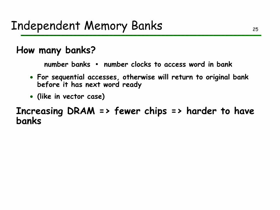
25Independent Memory Banks
How many banks?number banks number clocks to access word in bank
For sequential accesses, otherwise will return to original bank before it has next word ready
(like in vector case)
Increasing DRAM => fewer chips => harder to have banks

26DRAMs per PC over Time
Min
imum
Mem
ory
Siz
e
DRAM generation‘86 ‘89 ‘92 ‘96 ‘99 ‘02 1 Mb 4 Mb 16 Mb 64 Mb 256 Mb 1 Gb
4 MB
8 MB
16 MB
32 MB
64 MB
128 MB
256 MB
32 8
16 4
8 2
4 1
8 2
4 1
8 2
27
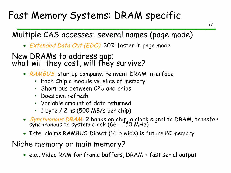
Fast Memory Systems: DRAM specific
Multiple CAS accesses: several names (page mode) Extended Data Out (EDO): 30% faster in page mode
New DRAMs to address gap; what will they cost, will they survive?
RAMBUS: startup company; reinvent DRAM interface Each Chip a module vs. slice of memory Short bus between CPU and chips Does own refresh Variable amount of data returned 1 byte / 2 ns (500 MB/s per chip)
Synchronous DRAM: 2 banks on chip, a clock signal to DRAM, transfer synchronous to system clock (66 - 150 MHz)
Intel claims RAMBUS Direct (16 b wide) is future PC memory
Niche memory or main memory? e.g., Video RAM for frame buffers, DRAM + fast serial output
28
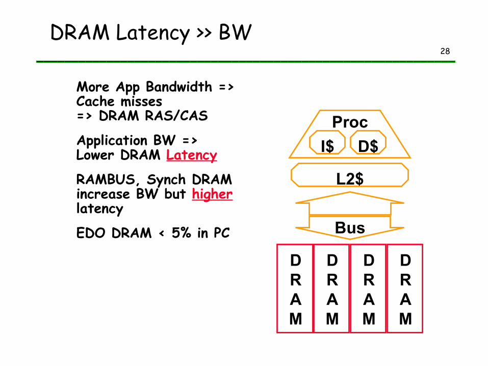
DRAM Latency >> BW
More App Bandwidth => Cache misses => DRAM RAS/CAS
Application BW => Lower DRAM Latency
RAMBUS, Synch DRAM increase BW but higher latency
EDO DRAM < 5% in PC
DRAM
DRAM
DRAM
DRAM
Bus
I$ D$
Proc
L2$
29
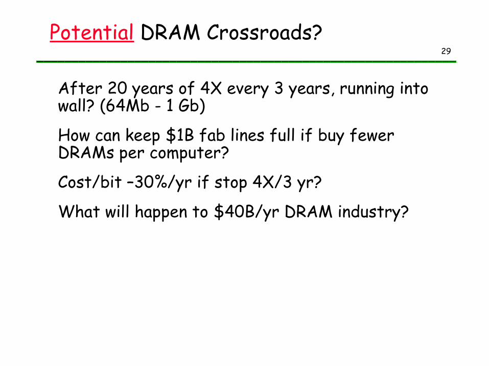
Potential DRAM Crossroads?
After 20 years of 4X every 3 years, running into wall? (64Mb - 1 Gb)
How can keep $1B fab lines full if buy fewer DRAMs per computer?
Cost/bit –30%/yr if stop 4X/3 yr?
What will happen to $40B/yr DRAM industry?
30
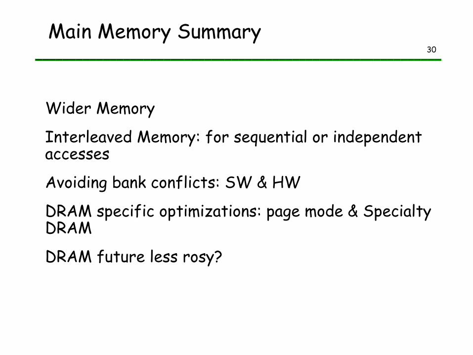
Main Memory Summary
Wider Memory
Interleaved Memory: for sequential or independent accesses
Avoiding bank conflicts: SW & HW
DRAM specific optimizations: page mode & Specialty DRAM
DRAM future less rosy?
31
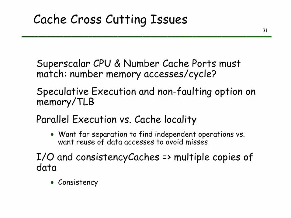
Cache Cross Cutting Issues
Superscalar CPU & Number Cache Ports must match: number memory accesses/cycle?
Speculative Execution and non-faulting option on memory/TLB
Parallel Execution vs. Cache locality Want far separation to find independent operations vs.
want reuse of data accesses to avoid misses
I/O and consistencyCaches => multiple copies of data
Consistency
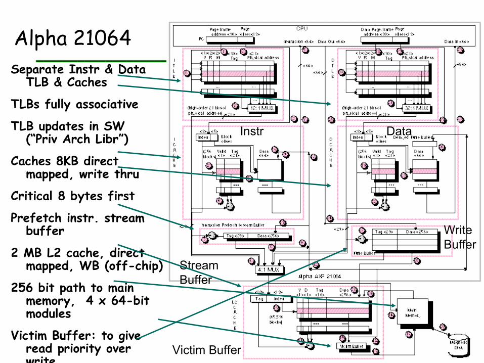
32Alpha 21064Separate Instr & Data
TLB & Caches
TLBs fully associative
TLB updates in SW(“Priv Arch Libr”)
Caches 8KB direct mapped, write thru
Critical 8 bytes first
Prefetch instr. stream buffer
2 MB L2 cache, direct mapped, WB (off-chip)
256 bit path to main memory, 4 x 64-bit modules
Victim Buffer: to give read priority over write
4 entry write buffer between D$ & L2$
StreamBuffer
WriteBuffer
Victim Buffer
Instr Data
33
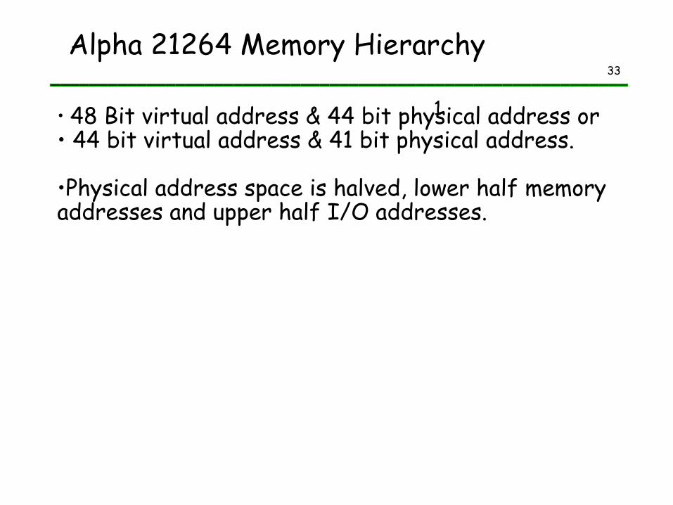
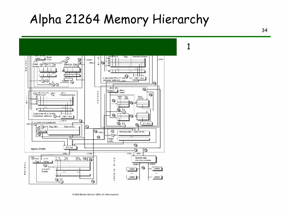
Alpha 21264 Memory Hierarchy
1• 48 Bit virtual address & 44 bit physical address or• 44 bit virtual address & 41 bit physical address.
•Physical address space is halved, lower half memory addresses and upper half I/O addresses.
34
Alpha 21264 Memory Hierarchy
1

35
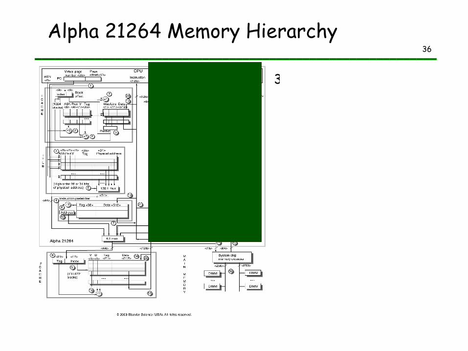
Alpha 21264 Memory Hierarchy
2
36
Alpha 21264 Memory Hierarchy
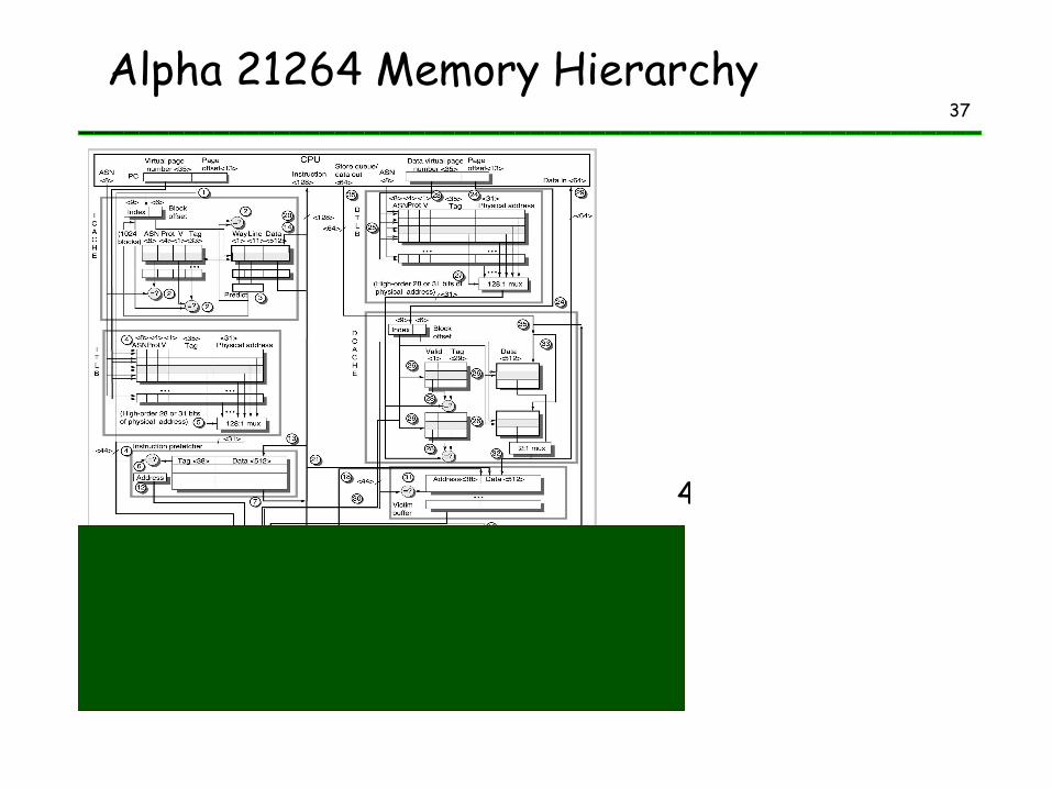
3
37
Alpha 21264 Memory Hierarchy
4

38
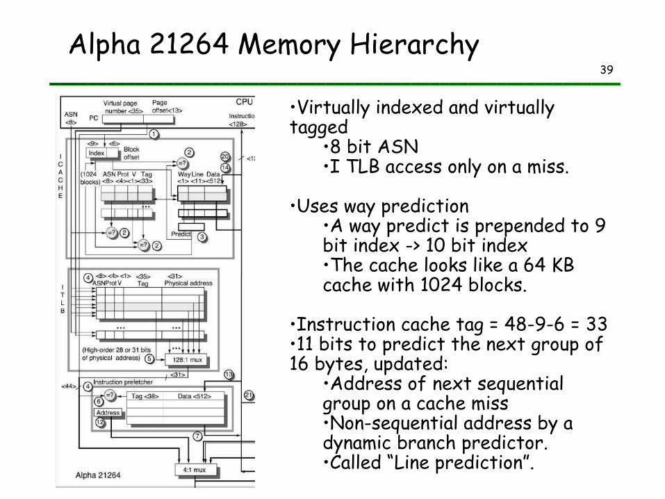
Alpha 21264 Memory Hierarchy - 1
ASN : Address space number.
Instruction cache interface
Store queue out
Data cache interface
39
Alpha 21264 Memory Hierarchy
•Virtually indexed and virtually tagged
•8 bit ASN•I TLB access only on a miss.
•Uses way prediction•A way predict is prepended to 9 bit index -> 10 bit index•The cache looks like a 64 KB cache with 1024 blocks.
•Instruction cache tag = 48-9-6 = 33•11 bits to predict the next group of 16 bytes, updated:
•Address of next sequential group on a cache miss•Non-sequential address by a dynamic branch predictor.•Called “Line prediction”.
40
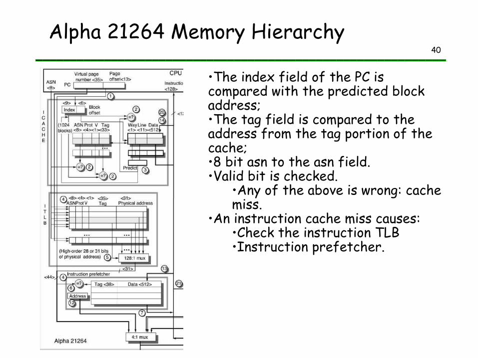
Alpha 21264 Memory Hierarchy
•The index field of the PC is compared with the predicted block address;•The tag field is compared to the address from the tag portion of the cache;•8 bit asn to the asn field.•Valid bit is checked.
•Any of the above is wrong: cache miss.
•An instruction cache miss causes:•Check the instruction TLB•Instruction prefetcher.

41
Alpha 21264 Memory Hierarchy
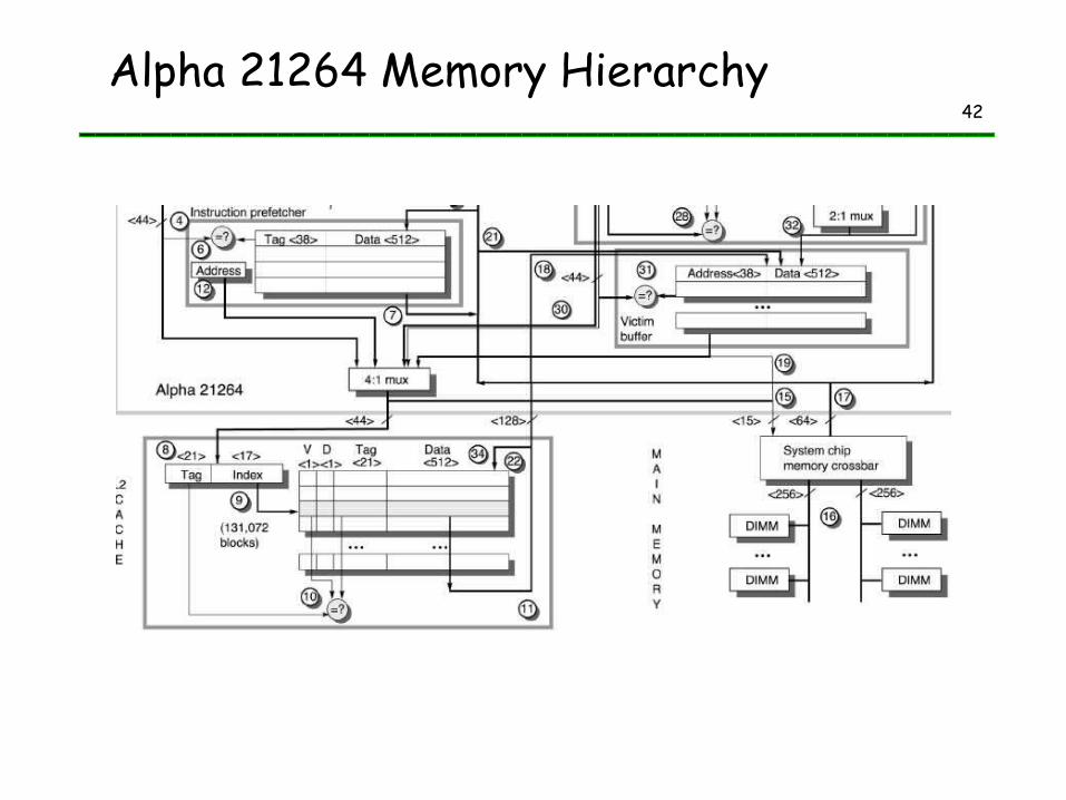
•Data cache is virtually indexed and physically tagged:
•9-bit index + 3 bits to select the appropriate 8 bytes are sent to the data cache;•Page frame of the address is sent to the TLB.
•Data TLB fully associative 128 PTEs.
42
Alpha 21264 Memory Hierarchy

43
0.01%
0.10%
1.00%
10.00%
100.00%AlphaSort Espresso Sc Mdljsp2 Ear Alvinn Mdljp2 Nasa7
Mis
s Rat
e
I $
D $
L2
Alpha Memory Performance: Miss Rates of SPEC92 (21064)
8K
8K
2M
I$ miss = 2%D$ miss = 13%L2 miss = 0.6%
I$ miss = 1%D$ miss = 21%L2 miss = 0.3%
I$ miss = 6%D$ miss = 32%L2 miss = 10%

44
0.00
0.50
1.00
1.50
2.00
2.50
3.00
3.50
4.00
4.50
5.00
AlphaSort Espresso Sc Mdljsp2 Ear Alvinn Mdljp2
CPI
L2
I$
D$
I Stall
Other
Alpha CPI ComponentsInstruction stall: branch mispredict (green);
Data cache (blue); Instruction cache (yellow); L2$ (pink) Other: compute + reg conflicts, structural conflicts
45
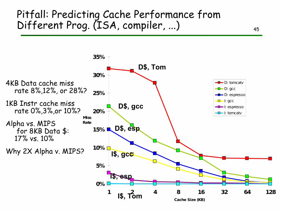
Pitfall: Predicting Cache Performance from Different Prog. (ISA, compiler, ...)
4KB Data cache miss rate 8%,12%, or 28%?
1KB Instr cache miss rate 0%,3%,or 10%?
Alpha vs. MIPS for 8KB Data $:17% vs. 10%
Why 2X Alpha v. MIPS?
0%
5%
10%
15%
20%
25%
30%
35%
1 2 4 8 16 32 64 128Cache Size (KB)
Miss Rate
D: tomcatv
D: gcc
D: espresso
I: gcc
I: espresso
I: tomcatv
D$, Tom
D$, gcc
D$, esp
I$, gcc
I$, esp
I$, Tom

46
Main Memory Summary
Wider Memory
Interleaved Memory: for sequential or independent accesses
Avoiding bank conflicts: SW & HW
DRAM specific optimizations: page mode & Specialty DRAM
DRAM future less rosy?
47
Practical Memory Hierarchy
Issue is NOT inventing new mechanisms
Issue is taste in selecting between many alternatives in putting together a memory hierarchy that fit well together
e.g., L1 Data cache write through, L2 Write back e.g., L1 small for fast hit time/clock cycle, e.g., L2 big enough to avoid going to DRAM?