Measurements and Characterization Tutorial - Surface ... · Measurements and Characterization...
25
Measurements and Characterization Tutorial Surface Analysis Characterization: Fundamentals and Applications to PV Joel Pankow NREL August 3, 2004
Transcript of Measurements and Characterization Tutorial - Surface ... · Measurements and Characterization...

Measurements and Characterization Tutorial
Surface Analysis Characterization:Fundamentals and Applications to PV
Joel PankowNREL
August 3, 2004

Electro-Optical Characterization
TeamRichard Ahrenkiel
Analytical Microscopy
TeamMowafak Al-Jassim
SurfaceAnalysis
TeamSarah Asher
Cell and Module Performance
TeamKeith Emery
National CenterFor Photovoltaics
Lawrence L. Kazmerski
Measurements & Characterization
DivisionPete Sheldon
Engineering and Reliability Division
Roland Hulstrom
Electronic Materials and
Devices DivisionJohn Benner
RD&D Alliances & Partnerships
Roland Hulstrom

Tutorial Outline
• What is surface analysis?• What are the various surface analysis tools available
within the surface analysis team?• What is meant by surface sensitivity and why does it
make surface analysis techniques unique and yet complementary to other techniques within M&C?
• Applications of the techniques toward furthering PV progress from team research projects, intra-division collaborations, industrial support/collaborations

What is Surface Analysis?
Surface analysis involves probing a sample with various chemical or physical probes and detecting the various characteristic emitted species to yield information about a surface. Typical probes include photon, electron or ion beams.

Surface Sensitivity
• Many analytical techniques used in materials characterization are “bulk” techniques in the sense that they give a composite measurement of the atoms in a sample.
• In contrast, a surface sensitive technique preferentially provides more sensitivity to atoms near the surface than in the bulk away from the surface i.e. the majority of the signal originates from the surface region.

TechniqueExcitation Source/Signal Detected
ElementsDetected
DetectionLimits
Depth Resolution
Lateral Resolution
Auger Electron Spectroscopy (AES)
Focused Electron Beam/Auger Electrons
Li to U 0.5 at.% 0-100Å**Auger electron escape depth
150Å
X-ray photoelectron Spectroscopy (XPS/ESCA)
Monochromatic X-rays/Photoemitted electronsand Auger electrons
Li to U 0.5 at.% 0-100Å 26µm
Secondary Ion Mass Spectrometry (SIMS)
Primary Ions (Cs, O, Ar)/ Secondary Ions
H to UAll elements and
isotopes
To 1 ppb(at/cm3)
<100Å 0.3µm
Static SIMS orTime-of-Flight SIMS (TOF-SIMS)
Primary Ions (Ar, Ga, O)/ Secondary Ions
H to UAll elements and
isotopes
To 1 ppm(at/cm3)
<50Å <0.2µm
Surface Analysis Team Capabilities

X-Ray Photoelectron Spectroscopy (XPS)(Photoemission Spectroscopy or ESCA (Electron Spectroscopy for Chemical Analysis)
XPS Basics:• Qualitative and Quantitative Information -
Photoelectrons occur at binding energies characteristic of elements present and at intensities proportional to their concentrations
• Chemical State Analysis – BE sensitive to valence states and molecular environments
• Surface Sensitive – Information depth < 100Å
• Angle Resolved XPS – Grazing take-off angles enhances fraction of signal from surface confined species
• Depth Profiling/Imaging – Analyzer “scans”to produce images

Applications of XPS to PV at NREL• Adhesive coated buss bar material
used in PV modules started to exhibit thermal hot spots in the field
• XPS examination of new buss bar quickly shows evidence of silicone release liner transfer on adhesive side and metal side of tape
• Depth profile of metal side shows layer of silicone material on top of oxidized tin and distinguishes tin oxide from metallic tin
Inte
nsity
(cps
)
14 00 12 00 1 000 800 600 400 200 0B in din g En ergy (e V)
Si 2p
C 1sO 1s
100
80
60
40
20
0
Atom
ic C
once
ntra
tion
43210Sputter Time (min)
O
Sn (metal)
Sn (oxide)C
Si
Inte
nsity
490 488 486 484 482Binding Energy (eV)

• CuInGaSe (CIGS) compounds represent an important class of PV absorber materials
• Experiments conducted using new integrated system in surface analysis lab
• Freshly etched surface using ammonia solution showed exclusive presence of Cu+1 but exposure to air showed gradual conversion of Cu+1 to Cu+2

• New polymer backsheet materials under investigation for PV packaging applications
• Polyethylene terphthalate (PET):
• Three clearly resolved forms of carbon and two resolved forms of oxygen evident in high resolution XPS scans
• Chemical functionalities can be altered by plasma and/or other treatments to enhance subsequent adhesion to PV encapsulants or other materials

Density of States
Intensity
Ultraviolet Photoelectron Spectroscopy (UPS)UPS Basics:• Chemical Bonding Information -
UPS probes only valence band energy levels and hence valence band (bonding) electrons
• Work Function Determination –Sensitive to surface contamination or adsorbed layers
• Surface Sensitive –Low mean escape depth

Auger Electron Spectroscopy (AES)AES Basics:• Qualitative and Quantitative Information -
Auger electrons occur at kinetic energies characteristic of elements present and at intensities proportional to their concentrations
• Surface Sensitive – Information depth limited to < 100Å
• Small feature analysis – Electron beam enables small spot size (15nm) and large magnification – point feature and composite analysis!
• Depth Profiling – Achieved by sputtering the surface with Ar+ ions. Useful for bulk analysis, diffusion, junctions, etc.
• Elemental Mapping and Line Scans –Achieved by rastering (map) or scanning electron beam and setting analyzer to detect selected elements
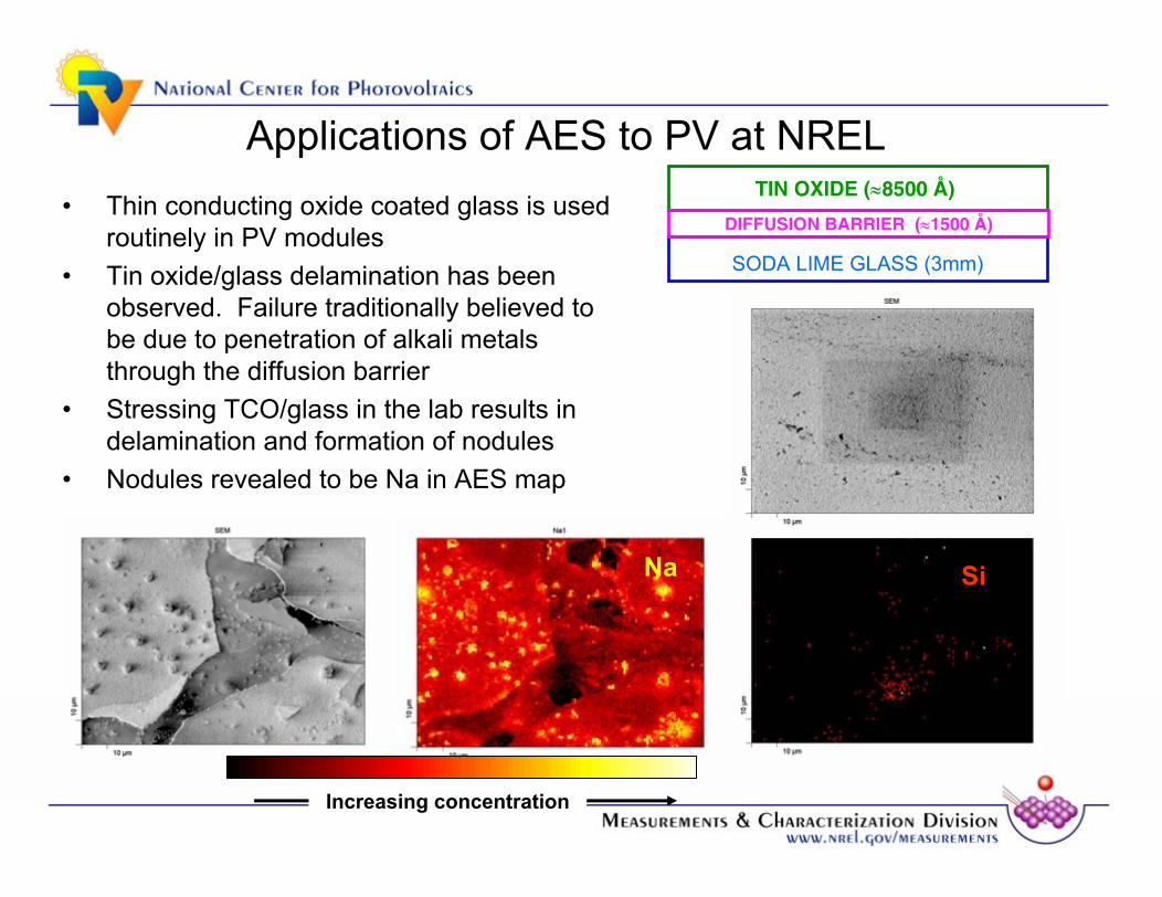
Applications of AES to PV at NRELTIN OXIDE (≈8500 Å)
DIFFUSION BARRIER (≈1500 Å)
SODA LIME GLASS (3mm)
• Thin conducting oxide coated glass is used routinely in PV modules
• Tin oxide/glass delamination has been observed. Failure traditionally believed to be due to penetration of alkali metals through the diffusion barrier
• Stressing TCO/glass in the lab results in delamination and formation of nodules
• Nodules revealed to be Na in AES map
Increasing concentration
Na Si
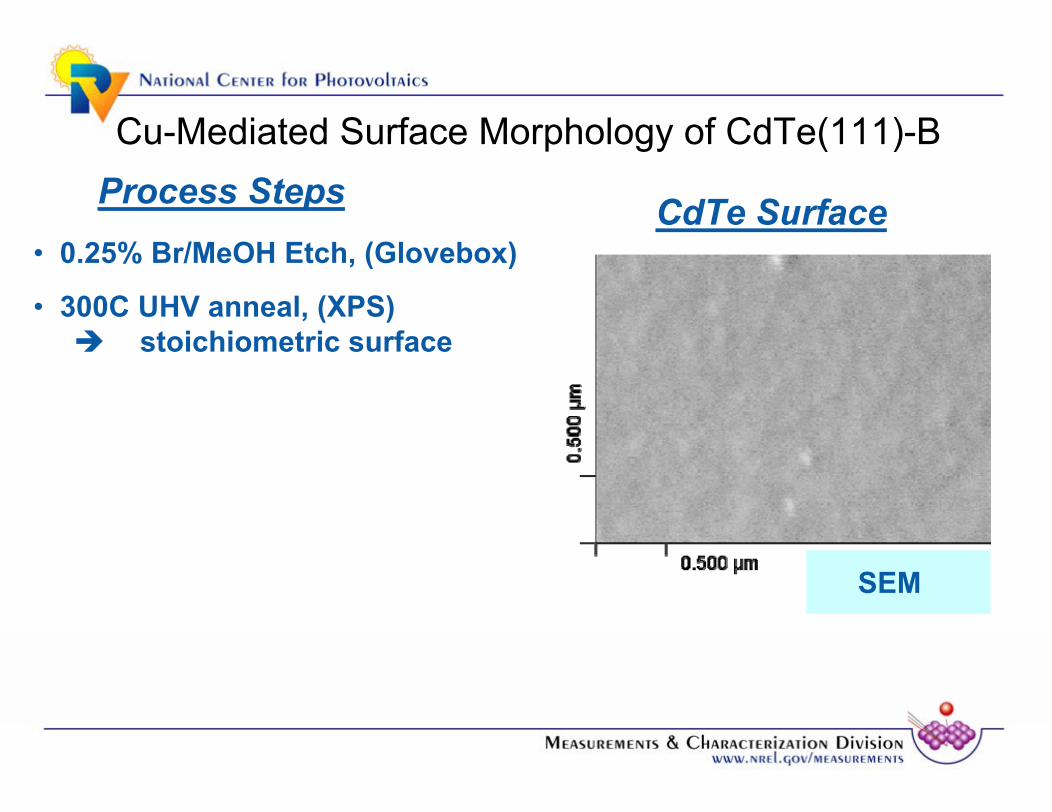
• 0.25% Br/MeOH Etch, (Glovebox)
Cu-Mediated Surface Morphology of CdTe(111)-B
SEM
Process Steps CdTe Surface
• 300C UHV anneal, (XPS)stoichiometric surface

• 0.25% Br/MeOH Etch, (Glovebox)
• 150 Å Cu, 300C (Dep. Chamber)Cu segregates at surface[111] surface w/ terraces
Cu-Mediated Surface Morphology of CdTe(111)-B
SEM
Process Steps CdTe Surface
• 300C UHV anneal, (XPS)stoichiometric surface

• 0.25% Br/MeOH Etch, (Glovebox)
• 150 Å Cu, 300C (Dep. Chamber)Cu segregates at surface[111] surface w/ terraces
Cu-Mediated Surface Morphology of CdTe(111)-B
SEM
• 300C Anneal, 3 Hr. (XPS)Cu diffuses into bulk nanoscale [110] facets form
• 300 Å Cu, 300C (Dep. Chamber)[111] facets reappeartriangular pits
Process Steps
AES map
CdTe Surface
Cu segregates on CdTe(111)-B and stabilizes [111] planes.
Cd Te Cu
• 300C UHV anneal, (XPS)stoichiometric surface

Secondary Ion Mass Spectrometry(SIMS)
Qualitative and Quantitative Information -Secondary ions occur at m/z ratios unique to the originating elements or molecular species. Ion yields are extremely matrix dependent (standards required for quantitation!)
• Detection of Hydrogen – Unique to SIMS• Examination of Isotopes – diffusion
experiments using D2O for example• Ultimate Surface Sensitivity – Monolayer
sampling depths• High Mass Resolution (m/∆m) - Important to
distinguish species with close m/z values• Superior Detection Limits – ppm to ppb• Small feature analysis – Raster size: 50 to
500 µm. Analysis size: 10 to 100 µm enables “ion imaging”
• Depth Profiling – Since emitted ions are examined (in contrast to AES & XPS) very fast sputter rates possible (upwards of 3000Å/min)

• O2 beam↑ + ion yield
• Cs beam↑ - ion yield
Positive and Negative Ion Yield vs. Periodic Table
1013
1014
1015
1016
1017
1018
Atom
s/cm
3
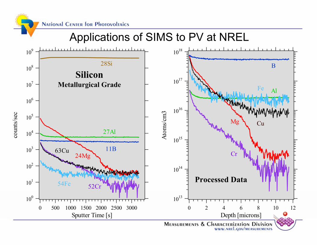
121086420Depth [microns]
Cr
CuMg
Al
B
Fe
100
101
102
103
104
105
106
107
108
109
coun
ts/se
c
300025002000150010005000Sputter Time [s]
28Si
24Mg
27Al 11B63Cu
54Fe 52Cr
SiliconMetallurgical Grade
Processed Data
Applications of SIMS to PV at NREL

1013
1014
1015
1016
1017
1018
1019
Con
cent
ratio
n [a
tom
s/cm
3]
20151050DEPTH [microns]
C
Fe
Al
Cr
SIMS Depth Profile and Post Scanning Ion Image
C
Fe
Al
Cr

Scanning Ion Images: Before and After O2 Depth Profile
Before After
C Al
Cr Fe
C Al
Cr Fe

Conclusions
• Surface analysis provide levels of surface sensitivity not possible with other techniques
• Degree of surface sensitivity determined by nature of specific technique
• Surface analytical techniques provide qualitative and quantitative information as well as spatial information and bulkdepth profiles
• Surface analytical data is rich in chemical information such as valence state or molecular environment, bonding information, surface “cleanliness” and more
• Surface analysis is routinely used at NREL to enable fundamental research, intra-division collaborative work and industrial support all designed to further PV progress
Acknowledgements
The Rest of the Surface Analysis Team:• Craig Perkins• Bob Reedy• Glenn Teeter• Matt Young• Sally Asher (Team Leader)