MC9S08LG32 Series - Data Sheet - NXP Semiconductors addendum identifies changes to Rev. 9 of the...
52
Freescale Semiconductor, Inc. Data Sheet: Technical Data © 2015 Freescale Semiconductor, Inc. All rights reserved. Rev. 10 of the MC9S08LG32 Series data sheet (covering MC9S08LG32 and MC9S08LG16) has two parts: • The addendum to revision 9 of the data sheet, immediately following this cover page. • Revision 9 of the data sheet, following the addendum. The changes described in the addendum have not been implemented in the specified pages. MC9S08LG32 Series with Addendum Covers: MC9S08LG32 and MC9S08LG16 Document Number: MC9S08LG32 Rev. 10, 04/2015
Transcript of MC9S08LG32 Series - Data Sheet - NXP Semiconductors addendum identifies changes to Rev. 9 of the...

Freescale Semiconductor, Inc.Data Sheet: Technical Data
© 2015 Freescale Semiconductor, Inc. All rights reserved.
Rev. 10 of the MC9S08LG32 Series data sheet (covering MC9S08LG32 and MC9S08LG16) has two parts:
• The addendum to revision 9 of the data sheet, immediately following this cover page.
• Revision 9 of the data sheet, following the addendum. The changes described in the addendum have not been implemented in the specified pages.
MC9S08LG32 Series with AddendumCovers: MC9S08LG32 and MC9S08LG16
Document Number: MC9S08LG32Rev. 10, 04/2015

Freescale Semiconductor, Inc.Data Sheet Addendum
© 2015 Freescale Semiconductor, Inc. All rights reserved.
This addendum identifies changes to Rev. 9 of the MC9S08LG32 Series data sheet (covering MC9S08LG32 and MC9S08LG16). The changes described in this addendum have not been implemented in the specified pages.
1 Add min values for IIC (DC injection current)
In Table 8, “DC Characteristics,” add min values for IIC (row number 14) as follows:
2 Change the max value of tLPO (low power oscillator period)
In Table 14, “Control Timing,” change the max value of tLPO (row number 2) from 1300 to 1500 µs.
Location: Table 8. DC Characteristics, Page 14
Num C Characteristic Symbol Min Typ1 Max Unit
14 D DC injection current 5, 6, 7
VIN < VSS (min)VIN > VDD (max)
Single pin limit IIC -0.2 — 2 mA
Total MCU limit, includes sum of all stressed pins
-5 — 25 mA
Location: Table 14. Control Timing, Page 29
Document Number: MC9S08LG32ADRev. 0, 04/2015
Addendum to Rev. 9 of the MC9S08LG32 SeriesCovers: MC9S08LG32 and MC9S08LG16

Freescale SemiconductorData Sheet: Technical Data
Document Number: MC9S08LG32Rev. 9 , 09/2011
MC9S08LG3280-LQFPCase 917A14 mm × 14 mm
64-LQFPCase 840F10 mm × 10 mm
48-LQFPCase 932
MC9S08LG32 SeriesCovers: MC9S08LG32 and MC9S08LG16
Features• 8-bit HCS08 Central Processor Unit (CPU)– Up to 40 MHz CPU at 5.5 V to 2.7 V across temperature range of –40 °C to 85 °C and –40 °C to 105 °C
– HCS08 instruction set with added BGND instruction– Support for up to 32 interrupt/reset sources
• On-Chip Memory– 32 KB or 18 KB dual array flash; read/program/erase
over full operating voltage and temperature– 1984 byte random access memory (RAM)– Security circuitry to prevent unauthorized access to
RAM and flash contents• Power-Saving Modes
– Two low-power stop modes (stop2 and stop3)– Reduced-power wait mode– Peripheral clock gating register can disable clocks to
unused modules, thereby reducing currents– Low power On-Chip crystal oscillator (XOSC) that can
be used in low-power modes to provide accurate clock source to real time counter and LCD controller
– 100 s typical wakeup time from stop3 mode• Clock Source Options
– Oscillator (XOSC) — Loop-control Pierce oscillator; crystal or ceramic resonator range of 31.25 kHz to 38.4 kHz or 1 MHz to 16 MHz
– Internal Clock Source (ICS) — Internal clock source module containing a frequency-locked-loop (FLL) controlled by internal or external reference; precision trimming of internal reference allows 0.2% resolution and 2% deviation over temperature and voltage; supports bus frequencies from 1 MHz to 20 MHz.
• System Protection– COP reset with option to run from dedicated 1 kHz
internal clock or bus clock– Low-voltage warning with interrupt– Low-voltage detection with reset– Illegal opcode detection with reset– Illegal address detection with reset– Flash and RAM protection
• Development Support– Single-wire background debug interface– Breakpoint capability to allow single breakpoint setting
during in-circuit debugging and plus two more breakpoints in On-Chip debug module
•
•
•
© Freescale Semiconductor, Inc., 2009-2011. All rights reserv
Freescale reserves the right to change the detail specificationimprovements in the design of its products.
7 mm × 7mm
– On-Chip in-circuit emulator (ICE) debug module containing three comparators and nine trigger modes; eight deep FIFO for storing change-of-flow addresses and event-only data; debug module supports both tag and force breakpoints
Peripherals– LCD — Up to 4 × 41 or 8 × 37 LCD driver with internal
charge pump.– ADC — Up to 16-channel, 12-bit resolution, 2.5 s
conversion time, automatic compare function, temperature sensor, internal bandgap reference channel, runs in stop3 and can wake up the system, fully functional from 5.5 V to 2.7 V
– SCI — Full duplex non-return to zero (NRZ), LIN master extended break generation, LIN slave extended break detection, wakeup on active edge
– SPI — Full-duplex or single-wire bidirectional, double-buffered transmit and receive, master or slave mode, MSB-first or LSB-first shifting
– IIC — With up to 100 kbps with maximum bus loading, multi-master operation, programmable slave address, interrupt driven byte-by-byte data transfer, supports broadcast mode and 10-bit addressing
– TPMx — One 6 channel and one 2 channel, selectable input capture, output compare, or buffered edge or center-aligned PWM on each channel
– MTIM — 8-bit counter with match register,, four clock sources with prescaler dividers, can be used for periodic wakeup
– RTC — 8-bit modulus counter with binary or decimal based prescaler, three clock sources including one external source, can be used for time base, calendar, or task scheduling functions
– KBI — One keyboard control module capable of supporting 8 × 8 keyboard matrix
– IRQ — External pin for wakeup from low-power modesInput/Output– 39, 53, or 69 GPIOs– 8 KBI and 1 IRQ interrupt with selectable polarity– Hysteresis and configurable pullup device on all input pins,
configurable slew rate and drive strength on all output pins.Package Options– 48-pin LQFP, 64-pin LQFP, and 80-pin LQFP
ed.
s as may be required to permit
MC9S08LG32 Series Data Sheet, Rev. 9
Freescale Semiconductor2
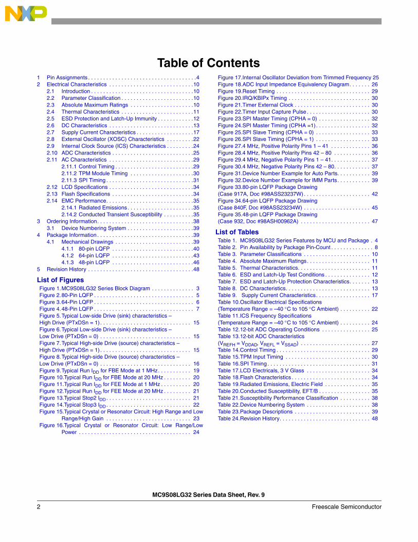
Table of Contents1 Pin Assignments . . . . . . . . . . . . . . . . . . . . . . . . . . . . . . . . . . . .42 Electrical Characteristics . . . . . . . . . . . . . . . . . . . . . . . . . . . .10
2.1 Introduction . . . . . . . . . . . . . . . . . . . . . . . . . . . . . . . . . .102.2 Parameter Classification . . . . . . . . . . . . . . . . . . . . . . . .102.3 Absolute Maximum Ratings . . . . . . . . . . . . . . . . . . . . .102.4 Thermal Characteristics . . . . . . . . . . . . . . . . . . . . . . . .112.5 ESD Protection and Latch-Up Immunity . . . . . . . . . . . .122.6 DC Characteristics . . . . . . . . . . . . . . . . . . . . . . . . . . . .132.7 Supply Current Characteristics . . . . . . . . . . . . . . . . . . .172.8 External Oscillator (XOSC) Characteristics . . . . . . . . .222.9 Internal Clock Source (ICS) Characteristics . . . . . . . . .242.10 ADC Characteristics . . . . . . . . . . . . . . . . . . . . . . . . . . .252.11 AC Characteristics . . . . . . . . . . . . . . . . . . . . . . . . . . . .29
2.11.1 Control Timing . . . . . . . . . . . . . . . . . . . . . . . . . .292.11.2 TPM Module Timing . . . . . . . . . . . . . . . . . . . . .302.11.3 SPI Timing . . . . . . . . . . . . . . . . . . . . . . . . . . . . .31
2.12 LCD Specifications . . . . . . . . . . . . . . . . . . . . . . . . . . . .342.13 Flash Specifications . . . . . . . . . . . . . . . . . . . . . . . . . . .342.14 EMC Performance. . . . . . . . . . . . . . . . . . . . . . . . . . . . .35
2.14.1 Radiated Emissions. . . . . . . . . . . . . . . . . . . . . .352.14.2 Conducted Transient Susceptibility . . . . . . . . . .35
3 Ordering Information. . . . . . . . . . . . . . . . . . . . . . . . . . . . . . . .383.1 Device Numbering System . . . . . . . . . . . . . . . . . . . . . .39
4 Package Information . . . . . . . . . . . . . . . . . . . . . . . . . . . . . . . .394.1 Mechanical Drawings . . . . . . . . . . . . . . . . . . . . . . . . . .39
4.1.1 80-pin LQFP . . . . . . . . . . . . . . . . . . . . . . . . . . .404.1.2 64-pin LQFP . . . . . . . . . . . . . . . . . . . . . . . . . . .434.1.3 48-pin LQFP . . . . . . . . . . . . . . . . . . . . . . . . . . .46
5 Revision History . . . . . . . . . . . . . . . . . . . . . . . . . . . . . . . . . . .48
List of FiguresFigure 1.MC9S08LG32 Series Block Diagram . . . . . . . . . . . . . . 3Figure 2.80-Pin LQFP . . . . . . . . . . . . . . . . . . . . . . . . . . . . . . . . . 5Figure 3.64-Pin LQFP . . . . . . . . . . . . . . . . . . . . . . . . . . . . . . . . . 6Figure 4.48-Pin LQFP . . . . . . . . . . . . . . . . . . . . . . . . . . . . . . . . . 7Figure 5.Typical Low-side Drive (sink) characteristics – High Drive (PTxDSn = 1) . . . . . . . . . . . . . . . . . . . . . . . . . . . . . . 15Figure 6.Typical Low-side Drive (sink) characteristics – Low Drive (PTxDSn = 0) . . . . . . . . . . . . . . . . . . . . . . . . . . . . . . 15Figure 7.Typical High-side Drive (source) characteristics – High Drive (PTxDSn = 1) . . . . . . . . . . . . . . . . . . . . . . . . . . . . . . 15Figure 8.Typical High-side Drive (source) characteristics –Low Drive (PTxDSn = 0) . . . . . . . . . . . . . . . . . . . . . . . . . . . . . . 16Figure 9.Typical Run IDD for FBE Mode at 1 MHz. . . . . . . . . . . 19Figure 10.Typical Run IDD for FBE Mode at 20 MHz . . . . . . . . . 20Figure 11.Typical Run IDD for FEE Mode at 1 MHz . . . . . . . . . . 20Figure 12.Typical Run IDD for FEE Mode at 20 MHz . . . . . . . . . 21Figure 13.Typical Stop2 IDD. . . . . . . . . . . . . . . . . . . . . . . . . . . . 21Figure 14.Typical Stop3 IDD. . . . . . . . . . . . . . . . . . . . . . . . . . . . 22Figure 15.Typical Crystal or Resonator Circuit: High Range and Low
Range/High Gain . . . . . . . . . . . . . . . . . . . . . . . . . . . . 23Figure 16.Typical Crystal or Resonator Circuit: Low Range/Low
Power . . . . . . . . . . . . . . . . . . . . . . . . . . . . . . . . . . . . . 24
Figure 17.Internal Oscillator Deviation from Trimmed Frequency 25Figure 18.ADC Input Impedance Equivalency Diagram. . . . . . . 26Figure 19.Reset Timing . . . . . . . . . . . . . . . . . . . . . . . . . . . . . . . 29Figure 20.IRQ/KBIPx Timing . . . . . . . . . . . . . . . . . . . . . . . . . . . 30Figure 21.Timer External Clock . . . . . . . . . . . . . . . . . . . . . . . . . 30Figure 22.Timer Input Capture Pulse . . . . . . . . . . . . . . . . . . . . . 30Figure 23.SPI Master Timing (CPHA = 0) . . . . . . . . . . . . . . . . . 32Figure 24.SPI Master Timing (CPHA =1) . . . . . . . . . . . . . . . . . . 32Figure 25.SPI Slave Timing (CPHA = 0) . . . . . . . . . . . . . . . . . . 33Figure 26.SPI Slave Timing (CPHA = 1) . . . . . . . . . . . . . . . . . . 33Figure 27.4 MHz, Positive Polarity Pins 1 – 41 . . . . . . . . . . . . . 36Figure 28.4 MHz, Positive Polarity Pins 42 – 80 . . . . . . . . . . . . 36Figure 29.4 MHz, Negative Polarity Pins 1 – 41. . . . . . . . . . . . . 37Figure 30.4 MHz, Negative Polarity Pins 42 – 80. . . . . . . . . . . . 37Figure 31.Device Number Example for Auto Parts. . . . . . . . . . . 39Figure 32.Device Number Example for IMM Parts. . . . . . . . . . . 39Figure 33.80-pin LQFP Package Drawing (Case 917A, Doc #98ASS23237W) . . . . . . . . . . . . . . . . . . . . . . 42Figure 34.64-pin LQFP Package Drawing (Case 840F, Doc #98ASS23234W) . . . . . . . . . . . . . . . . . . . . . . 45Figure 35.48-pin LQFP Package Drawing (Case 932, Doc #98ASH00962A) . . . . . . . . . . . . . . . . . . . . . . . 47
List of TablesTable 1. MC9S08LG32 Series Features by MCU and Package . 4Table 2. Pin Availability by Package Pin-Count . . . . . . . . . . . . . . 8Table 3. Parameter Classifications . . . . . . . . . . . . . . . . . . . . . . 10Table 4. Absolute Maximum Ratings. . . . . . . . . . . . . . . . . . . . . 11Table 5. Thermal Characteristics. . . . . . . . . . . . . . . . . . . . . . . . 11Table 6. ESD and Latch-Up Test Conditions . . . . . . . . . . . . . . . 12Table 7. ESD and Latch-Up Protection Characteristics. . . . . . . 13Table 8. DC Characteristics. . . . . . . . . . . . . . . . . . . . . . . . . . . . 13Table 9. Supply Current Characteristics. . . . . . . . . . . . . . . . . . 17Table 10.Oscillator Electrical Specifications (Temperature Range = –40 C to 105 C Ambient) . . . . . . . . . . 22Table 11.ICS Frequency Specifications (Temperature Range = –40 C to 105 C Ambient) . . . . . . . . . . 24Table 12.12-bit ADC Operating Conditions . . . . . . . . . . . . . . . . 25Table 13.12-bit ADC Characteristics (VREFH = VDDAD, VREFL = VSSAD) . . . . . . . . . . . . . . . . . . . . . . . 27Table 14.Control Timing . . . . . . . . . . . . . . . . . . . . . . . . . . . . . . . 29Table 15.TPM Input Timing . . . . . . . . . . . . . . . . . . . . . . . . . . . . 30Table 16.SPI Timing . . . . . . . . . . . . . . . . . . . . . . . . . . . . . . . . . . 31Table 17.LCD Electricals, 3 V Glass . . . . . . . . . . . . . . . . . . . . . 34Table 18.Flash Characteristics . . . . . . . . . . . . . . . . . . . . . . . . . . 34Table 19.Radiated Emissions, Electric Field . . . . . . . . . . . . . . . 35Table 20.Conducted Susceptibility, EFT/B . . . . . . . . . . . . . . . . . 35Table 21.Susceptibility Performance Classification . . . . . . . . . . 38Table 22.Device Numbering System . . . . . . . . . . . . . . . . . . . . . 38Table 23.Package Descriptions . . . . . . . . . . . . . . . . . . . . . . . . . 39Table 24.Revision History. . . . . . . . . . . . . . . . . . . . . . . . . . . . . . 48

Figure 1. MC9S08LG32 Series Block Diagram
8-BIT KEYBOARDINTERRUPT (KBI)
IIC MODULE (IIC)
SERIAL PERIPHERAL INTERFACE (SPI)
USER FLASH B
USER RAM
On-Chip ICE (ICE) andDEBUG MODULE (DBG)
(LG32 = 16K BYTES)
HCS08 CORE
CPU
BKGD
INT
BKP
2-CHANNEL TIMER/PWM
(TPM1)
HCS08 SYSTEM CONTROL
RESETS AND INTERRUPTSMODES OF OPERATIONPOWER MANAGEMENT
IRQ LVD
LOW-POWER OSCILLATOR
INTERNAL CLOCKSource (ICS)
SERIAL COMMUNICATIONS
6-CHANNEL TIMER/PWM
(TPM2)
VLL3
(LCD)
VLL1
VLL2
VCAP1
VCAP2
LCD[44:0]
VSS
VDD
VOLTAGE
REGULATOR
USER FLASH A
(LG16 = 2K BYTES)
LCD28/ADC5/TPMCLK/PTA7LCD27/ADC4/TPM2CH1/KBI7/PTA6
LCD25/ADC2/RX2/KBI5/PTA4
INTERFACE (SCI1)
TxD1
RxD1
SSSPSCK
SCL
SDA
MOSI
MISO
VSSA/VREFL
VDDA/VREFH
XTAL
EXTAL
IRQ
KBI[7:0]
PO
RT
A
RESET
LIQUID CRYSTALDISPLAY DRIVER
ANALOG-TO-DIGITALCONVERTER (ADC)
12-BITAD[15:0]
TPM2CH[5:0]
TPMCLK
TPMCLK
LCD24/ADC1/TX2/KBI4/PTA3LCD23/ADC0/SDA/PTA2LCD22/SCL/PTA1LCD21/PTA0
(LG32 = 16K BYTES)
(LG16 = 16K BYTES)
LCD26/ADC3/TPM2CH0/KBI6/PTA5
BKGD/MS
TPM1CH[1:0]
COP
Real Time Counter
(RTC)
TMRCLK
SERIAL COMMUNICATIONS
INTERFACE (SCI2)
TxD2
RxD2
PO
RT
C
EXTAL/PTF7XTAL/PTF6
TPM2CH4/KBI1/MISO/PTF4
PO
RT
F
TPM2CH5/KBI0/SS/PTF3ADC14/IRQ/TPM1CH1/SPSCK/PTF2ADC13/TPM1CH0/RX1/PTF1ADC12/TPM2CH2/KBI3/TX1/PTF0
TPM2CH3/KBI2/MOSI/PTF5
SPSCK/SDA/TPM2CH1/PTI4
PO
RT
I
MOSI/TPM2CH2/PTI3MISO/TPM2CH3/PTI2TX2/TMRCLK/PTI1RX2/PTI0
SS/SCL/TPM2CH0/PTI5
PO
RT
DP
OR
T E
LCD[40:37]/PTB[7:4]LCD[32:29]/PTB[3:0]
LCD[7:0]/PTD[7:0]
PO
RT
B
LCD[15:8]/PTE[7:0]
LCD[44:41]/PTG[7:4]LCD[36:33]/PTG[3:0]
PO
RT
G
ADC11/TPM1CH0/KBI3/TX1/PTH5ADC10/TPM1CH1/KBI2/RX1/PTH4ADC[9:6]/KBI[7:4]/PTH[3:0]
TPM2CH4/KBI1/PTH7ADC15/KBI0/TPM2CH5/PTH6
PO
RT
H
VSS2
VLL3_2
Available only on 80-pin packageAvailable only on 64-pin and 80-pin package
*/Default function out of reset/*
BKGD/MS/PTC5RESET/PTC6
Modulo Timer
(MTIM)
1984 BYTES
LCD[20:16]/PTC[4:0]
MC9S08LG32 Series Data Sheet, Rev. 9
Freescale Semiconductor 3

Pin Assignments
1 Pin AssignmentsThis section shows the pin assignments for the MC9S08LG32 series devices. The priority of functions on a pin is in ascending order from left to right and bottom to top. Another view of pinouts and function priority is given in Table 2.
Table 1. MC9S08LG32 Series Features by MCU and Package
Feature MC9S08LG32 MC9S08LG16
Flash size (bytes) 32,768 18,432
RAM size (bytes) 1984
Pin quantity 80 64 48 64 48
ADC 16 ch 12 ch 9 ch 12 ch 9 ch
LCD 8 x 374 x 41
8 x 294 x 33
8 x 214 x 25
8 x 294 x 33
8 x 214 x 25
ICE + DBG yes
ICS yes
IIC yes
IRQ yes
KBI 8 pin
GPIOs 69 53 39 53 39
RTC yes
MTIM yes
SCI1 yes
SCI2 yes
SPI yes
TPM1 channels 2
TPM2 channels 6
XOSC yes
MC9S08LG32 Series Data Sheet, Rev. 9
Freescale Semiconductor4

Pin Assignments
Figure 2. 80-Pin LQFP
NOTEVREFH/VREFL are internally connected to VDDA/VSSA.
1234567891011121314151617181920
21 22 23 24 25 26 27 28 29 30 31 32 33 34 35 36 37 38 39 40
80-Pin LQFP
PT
E0/
LCD
8P
TE
1/LC
D9
PT
E2/
LCD
10P
TE
3/LC
D11
PT
E4/
LCD
12P
TE
5/LC
D13
PT
G0/
LCD
33P
TG
1/LC
D34
PT
G4/
LCD
41P
TG
5/LC
D42
PT
G6/
LCD
43P
TG
7/LC
D44
VLL
3_2
VS
S2
PT
E6/
LCD
14P
TE
7/LC
D15
PT
C0/
LCD
16P
TC
1/LC
D17
PT
C2/
LCD
18P
TC
3/LC
D19
PTD7/LCD7PTD6/LCD6PTD5/LCD5PTD4/LCD4PTD3/LCD3PTD2/LCD2
PTB3/LCD32PTB2/LCD31PTB7/LCD40PTB6/LCD39PTB5/LCD38PTB4/LCD37PTB1/LCD30PTB0/LCD29PTD1/LCD1PTD0/LCD0
VCAP1VCAP2
VLL1VLL2
VLL
3P
TF
5/M
OS
I/KB
I2/T
PM
2CH
3P
TF
4/M
ISO
/KB
I1/T
PM
2CH
4P
TI5
/TP
M2C
H0/
SC
L/S
SP
TI4
/TP
M2C
H1/
SD
A/S
PS
CK
PT
I3/T
PM
2CH
2/M
OS
IP
TI2
/TP
M2C
H3/
MIS
OP
TI1
/TM
RC
LK/T
X2
PT
I0/R
X2
PT
H7/
KB
I1/T
PM
2CH
4V
SS
VD
DP
TF
7/E
XTA
LP
TF
6/X
TAL
VD
DA/V
RE
FH
VS
SA/V
RE
FL
PT
H6/
TP
M2C
H5/
KB
I0/A
DC
15P
TF
2/S
PS
CK
/TP
M1C
H1/
IRQ
/AD
C14
PT
F1/
RX
1/T
PM
1CH
0/A
DC
13P
TF
0/T
X1/
KB
I3/T
PM
2CH
2/A
DC
12
6059585756555453525150494847464544434241
PTC4/LCD20PTA0/LCD21PTG2/LCD35PTG3/LCD36PTA1/SCL/LCD22PTA2/SDA/ADC0/LCD23PTA3/KBI4/TX2/ADC1/LCD24PTA4/KBI5/RX2/ADC2/LCD25PTA5/KBI6/TPM2CH0/ADC3/LCD26PTA6/KBI7/TPM2CH1/ADC4/LCD27PTA7/TPMCLK/ADC5/LCD28PTC5/BKGD/MSPTC6/RESETPTH0/KBI4/ADC6PTH1/KBI5/ADC7PTH2KBI6/ADC8PTH3/KBI7/ADC9PTH4/RX1/KBI2/TPM1CH1/ADC10PTH5/TX1/KBI3/TPM1CH0/ADC11PTF3/SS/KBI0/TPM2CH5
80 79 78 77 76 75 74 73 72 71 70 69 68 67 66 65 64 63 62 61
MC9S08LG32 Series Data Sheet, Rev. 9
Freescale Semiconductor 5

Pin Assignments
Figure 3. 64-Pin LQFP
NOTEVREFH/VREFL are internally connected to VDDA/VSSA.
12345678910111213141516
17 18 19 20 21 22 23 24 25 26 27 28 29 30 31 32
64-Pin LQFPP
TE
0/LC
D8
PT
E1/
LCD
9P
TE
2/LC
D10
PT
E3/
LCD
11P
TE
4/LC
D12
PT
E5/
LCD
13P
TG
0/LC
D33
PT
G1/
LCD
34V
LL3_
2V
SS
2P
TE
6/LC
D14
PT
E7/
LCD
15P
TC
0/LC
D16
PT
C1/
LCD
17P
TC
2/LC
D18
PT
C3/
LCD
19
PTD7/LCD7PTD6/LCD6PTD5/LCD5PTD4/LCD4PTD3/LCD3PTD2/LCD2
PTB3/LCD32PTB2/LCD31PTB1/LCD30PTB0/LCD29PTD1/LCD1PTD0/LCD0
VCAP1VCAP2
VLL1VLL2
VLL
3P
TF
5/M
OS
I/KB
I2/T
PM
2CH
3P
TF
4/M
ISO
/KB
I1/T
PM
2CH
4P
TI5
/TP
M2C
H0/
SC
L/S
SP
TI4
/TP
M2C
H1/
SD
A/S
PS
CK
PT
H7/
KB
I1/T
PM
2CH
4V
SS
VD
DP
TF
7/E
XTA
LP
TF
6/X
TAL
VD
DA/V
RE
FH
VS
SA/V
RE
FL
PT
H6/
TP
M2C
H5/
KB
I0/A
DC
15P
TF
2/S
PS
CK
/TP
M1C
H1/
IRQ
/AD
C14
PT
F1/
RX
1/T
PM
1CH
0/A
DC
13P
TF
0/T
X1/
KB
I3/T
PM
2CH
2/A
DC
12
48474645444342414039383736353433
64 63 62 61 60 59 58 57 56 55 54 53 52 51 50 49 PTC4/LCD20PTA0/LCD21PTG2/LCD35PTG3/LCD36PTA1/SCL/LCD22PTA2/SDA/ADC0/LCD23PTA3/KBI4/TX2/ADC1/LCD24PTA4/KBI5/RX2/ADC2/LCD25PTA5/KBI6/TPM2CH0/ADC3/LCD26PTA6/KBI7/TPM2CH1/ADC4/LCD27PTA7/TPMCLK/ADC5/LCD28PTC5/BKGD/MSPTC6/RESETPTH4/RX1/KBI2/TPM1CH1/ADC10PTH5/TX1/KBI3/TPM1CH0/ADC11PTF3/SS/KBI0/TPM2CH5
MC9S08LG32 Series Data Sheet, Rev. 9
Freescale Semiconductor6

Pin Assignments
Figure 4. 48-Pin LQFP
NOTEVREFH/VREFL are internally connected to VDDA/VSSA.
PTD0/LCD0
1
2
3
4
5
6
7
8
PTD3/LCD3
VD
DA/V
RE
FH
PT
F6/
XTA
L
V DD
VS
S
PT
F4/
MIS
O/K
BI1
/TP
M2C
H4
PT
F5/
MO
SI/K
BI2
/TP
M2C
H3
PTA7/TPMCLK/ADC5/LCD28
PTC6/RESETP
TC
2/LC
D18
PT
E7/
LCD
15
PT
C0/
LCD
16
PT
C1/
LCD
17
31
30
29
28
27
26
14 15 17 18 19
37
3839
13 24
25
36
48
9
10
11
VCAP1
12VLL2
VS
SA/V
RE
FL
20
PT
F2/
SP
SC
KS
/TP
M1C
H1/
IRQ
/AD
C14
21
PT
F1/
RX
1/T
PM
1CH
0/A
DC
13
22 23
PTC5/BKGD/MS
PT
E6/
LCD
14
40
PT
E5/
LCD
13
41
PT
E4/
LCD
12
42
PT
E3/
LCD
11
43
PTD2/LCD2
VCAP2
VLL1
32
33
34
35P
TE
1/LC
D9
47 46 45
PT
E2/
LCD
10
44
PTD5/LCD5
PTD4/LCD4
VLL
3
PTF3/SS/KBI0/TPM2CH5P
TC
3/LC
D19
48-Pin LQFP
PTD1/LCD1
PTD7/LCD7
PTD6/LCD6
PTA1/SCL/LCD22
PTA2/SDA/ADC0/LCD23
PTA3/KBI4/TX2/ADC1/LCD24
PTA4/KBI5/RX2/ADC2/LCD25
PTA6/KBI7/TPM2CH1/ADC4/LCD27
PTA5/KBI6/TPM2CH0/ADC3/LCD26
PTC4/LCD20
PTA0/LCD21
PT
E0/
LCD
8
PT
F0/
TX
1/K
BI3
/TP
M2C
H2/
AD
C12
16
PT
F7/
EX
TAL
MC9S08LG32 Series Data Sheet, Rev. 9
Freescale Semiconductor 7

Pin Assignments
Table 2. Pin Availability by Package Pin-Count
Packages <-- Lowest Priority --> Highest
80 64 48 Port Pin Alt 1 Alt 2 Alt 3 Alt 4
1 1 1 PTD7 LCD7 — — —
2 2 2 PTD6 LCD6 — — —
3 3 3 PTD5 LCD5 — — —
4 4 4 PTD4 LCD4 — — —
5 5 5 PTD3 LCD3 — — —
6 6 6 PTD2 LCD2 — — —
7 7 — PTB3 LCD32 — — —
8 8 — PTB2 LCD31 — — —
9 — — PTB7 LCD40 — — —
10 — — PTB6 LCD39 — — —
11 — — PTB5 LCD38 — — —
12 — — PTB4 LCD37 — — —
13 9 — PTB1 LCD30 — — —
14 10 — PTB0 LCD29 — — —
15 11 7 PTD1 LCD1 — — —
16 12 8 PTD0 LCD0 — — —
17 13 9 VCAP1 — — — —
18 14 10 VCAP2 — — — —
19 15 11 VLL1 — — — —
20 16 12 VLL2 — — — —
21 17 13 VLL3 — — — —
22 18 14 PTF5 MOSI KBI2 TPM2CH3 —
23 19 15 PTF4 MISO KBI1 TPM2CH4 —
24 20 — PTI5 TPM2CH0 SCL SS —
25 21 — PTI4 TPM2CH1 SDA SPSCK —
26 — — PTI3 TPM2CH2 MOSI — —
27 — — PTI2 TPM2CH3 MISO — —
28 — — PTI1 TMRCLK TX2 — —
29 — — PTI0 RX2 — — —
30 22 — PTH7 KBI1 TPM2CH4 — —
31 23 16 VSS — — — —
32 24 17 VDD — — — —
33 25 18 PTF7 EXTAL — — —
34 26 19 PTF6 XTAL — — —
35 27 20 VDDA VREFH — — —
36 28 21 VSSA VREFL — — —
37 29 — PTH6 TPM2CH5 KBI0 ADC15 —
38 30 22 PTF2 SPSCK TPM1CH1 IRQ ADC14
MC9S08LG32 Series Data Sheet, Rev. 9
Freescale Semiconductor8

Pin Assignments
39 31 23 PTF1 RX1 TPM1CH0 ADC13 —
40 32 24 PTF0 TX1 KBI3 TPM2CH2 ADC12
41 33 25 PTF3 SS KBI0 TPM2CH5 —
42 34 — PTH5 TX1 KBI3 TPM1CH0 ADC11
43 35 — PTH4 RX1 KBI2 TPM1CH1 ADC10
44 — — PTH3 KBI7 ADC9 — —
45 — — PTH2 KBI6 ADC8 — —
46 — — PTH1 KBI5 ADC7 — —
47 — — PTH0 KBI4 ADC6 — —
48 36 26 PTC6 RESET — — —
49 37 27 PTC5 BKGD/MS — — —
50 38 28 PTA7 TPMCLK ADC5 LCD28 —
51 39 29 PTA6 KBI7 TPM2CH1 ADC4 LCD27
52 40 30 PTA5 KBI6 TPM2CH0 ADC3 LCD26
53 41 31 PTA4 KBI5 RX2 ADC2 LCD25
54 42 32 PTA3 KBI4 TX2 ADC1 LCD24
55 43 33 PTA2 SDA ADC0 LCD23 —
56 44 34 PTA1 SCL LCD22 — —
57 45 — PTG3 LCD36 — — —
58 46 — PTG2 LCD35 — — —
59 47 35 PTA0 LCD21 — — —
60 48 36 PTC4 LCD20 — — —
61 49 37 PTC3 LCD19 — — —
62 50 38 PTC2 LCD18 — — —
63 51 39 PTC1 LCD17 — — —
64 52 40 PTC0 LCD16 — — —
65 53 41 PTE7 LCD15 — — —
66 54 42 PTE6 LCD14 — — —
67 55 — VSS2 — — — —
68 56 — VLL3_2 — — — —
69 — — PTG7 LCD44 — — —
70 — — PTG6 LCD43 — — —
71 — — PTG5 LCD42 — — —
72 — — PTG4 LCD41 — — —
73 57 — PTG1 LCD34 — — —
74 58 — PTG0 LCD33 — — —
75 59 43 PTE5 LCD13 — — —
76 60 44 PTE4 LCD12 — — —
Table 2. Pin Availability by Package Pin-Count (continued)
Packages <-- Lowest Priority --> Highest
80 64 48 Port Pin Alt 1 Alt 2 Alt 3 Alt 4
MC9S08LG32 Series Data Sheet, Rev. 9
Freescale Semiconductor 9

Electrical Characteristics
2 Electrical Characteristics
2.1 IntroductionThis section contains electrical and timing specifications for the MC9S08LG32 series of microcontrollers available at the time of publication.
2.2 Parameter ClassificationThe electrical parameters shown in this supplement are guaranteed by various methods. To give the customer a better understanding the following classification is used and the parameters are tagged accordingly in the tables where appropriate:
NOTEThe classification is shown in the column labeled “C” in the parameter tables where appropriate.
2.3 Absolute Maximum RatingsAbsolute maximum ratings are stress ratings only, and functional operation at the maxima is not guaranteed. Stress beyond the limits specified in Table 4 may affect device reliability or cause permanent damage to the device. For functional operating conditions, refer to the remaining tables in this section.
This device contains circuitry that protects against damage due to high static voltage or electrical fields. However, it is advised that normal precautions should be taken to avoid application of any voltages higher than maximum-rated voltages to this high-impedance circuit. Reliability of operation is enhanced if unused inputs are tied to an appropriate logic voltage level (for instance, either VSS or VDD) or the programmable pull-up resistor associated with the pin is enabled.
77 61 45 PTE3 LCD11 — — —
78 62 46 PTE2 LCD10 — — —
79 63 47 PTE1 LCD9 — — —
80 64 48 PTE0 LCD8 — — —
Table 3. Parameter Classifications
P Those parameters are guaranteed during production testing on each individual device.
CThose parameters are achieved by the design characterization by measuring a statistically relevant sample size across process variations.
TThose parameters are achieved by design characterization on a small sample size from typical devices under typical conditions unless otherwise noted. All values shown in the typical column are within this category.
D Those parameters are derived mainly from simulations.
Table 2. Pin Availability by Package Pin-Count (continued)
Packages <-- Lowest Priority --> Highest
80 64 48 Port Pin Alt 1 Alt 2 Alt 3 Alt 4
MC9S08LG32 Series Data Sheet, Rev. 9
Freescale Semiconductor10

Electrical Characteristics
2.4 Thermal CharacteristicsThis section provides information about operating temperature range, power dissipation, and package thermal resistance. Power dissipation on I/O pins is usually small compared to the power dissipation in On-Chip logic and voltage regulator circuits, and it is user-determined rather than being controlled by the MCU design. To take PI/O into account in power calculations, determine the difference between actual pin voltage and VSS or VDD and multiply by the pin current for each I/O pin. Except in cases of unusually high pin current (heavy loads), the difference between pin voltage and VSS or VDD will be very small.
The average chip-junction temperature (TJ) in C can be obtained from:
TJ = TA + (PD JA) Eqn. 1
Table 4. Absolute Maximum Ratings
Rating Symbol Value Unit
Supply voltage VDD –0.3 to +5.8 V
Maximum current into VDD IDD 120 mA
Digital input voltage VIn –0.3 to VDD + 0.3 V
Instantaneous maximum current Single pin limit (applies to all port pins)1, 2, 3
1 Input must be current limited to the value specified. To determine the value of the required current-limiting resistor, calculate resistance values for positive (VDD) and negative (VSS) clamp voltages and use the largest of the two resistance values.
2 All functional non-supply pins are internally clamped to VSS and VDD.3 Power supply must maintain regulation within operating VDD range during instantaneous and
operating maximum current conditions. If positive injection current (VIn > VDD) is greater than IDD, the injection current may flow out of VDD and could result in an external power supply going out of regulation. Ensure that the external VDD load will shunt current greater than maximum injection current, this will be of greater risk when the MCU is not consuming power. For instance, if no system clock is present, or if the clock rate is very low (which would reduce overall power consumption).
ID 252
mA
Storage temperature range Tstg –55 to 150 C
Table 5. Thermal Characteristics
Rating Symbol Value Unit
Operating temperature range (packaged)
TA TL to TH–40 to +105
C
Maximum junction temperature TJ 125 C
Thermal resistanceSingle-layer board
80-pin LQFP64-pin LQFP48-pin LQFP
JA 617180
C/W
Thermal resistanceFour-layer board
80-pin LQFP64-pin LQFP48-pin LQFP
JA 485256
C/W
MC9S08LG32 Series Data Sheet, Rev. 9
Freescale Semiconductor 11

Electrical Characteristics
where:
TA = Ambient temperature, CJA = Package thermal resistance, junction-to-ambient, C/W
PD = Pint PI/O
Pint = IDD VDD, Watts — chip internal power
PI/O = Power dissipation on input and output pins — user determined
For most applications, PI/O Pint and can be neglected. An approximate relationship between PD and TJ (if PI/O is neglected) is:
PD = K (TJ + 273 C) Eqn. 2
Solving Equation 1 and Equation 2 for K gives:
K = PD (TA + 273C) + JA (PD)2 Eqn. 3
where K is a constant pertaining to the particular part. K can be determined from equation 3 by measuring PD (at equilibrium) for a known TA. Using this value of K, the values of PD and TJ can be obtained by solving Equation 1 and Equation 2 iteratively for any value of TA.
2.5 ESD Protection and Latch-Up ImmunityAlthough damage from electrostatic discharge (ESD) is much less common on these devices than on early CMOS circuits, normal handling precautions should be taken to avoid exposure to static discharge. Qualification tests are performed to ensure that these devices can withstand exposure to reasonable levels of static without suffering any permanent damage.
All ESD testing is in conformity with AEC-Q100 Stress Test Qualification for automotive grade integrated circuits. During the device qualification, ESD stresses were performed for the human body model (HBM), the machine model (MM) and the charge device model (CDM).
A device is defined as a failure if after exposure to ESD pulses the device no longer meets the device specification. Complete DC parametric and functional testing is performed per the applicable device specification at room temperature followed by hot temperature, unless instructed otherwise in the device specification.
Table 6. ESD and Latch-Up Test Conditions
Model Description Symbol Value Unit
Human Body Model
Series resistance R1 1500
Storage capacitance C 100 pF
Number of pulses per pin — 3 —
Latch-up Minimum input voltage limit — –2.5 V
Maximum input voltage limit — 7.5 V
MC9S08LG32 Series Data Sheet, Rev. 9
Freescale Semiconductor12

Electrical Characteristics
2.6 DC CharacteristicsThis section includes information about power supply requirements and I/O pin characteristics.
Table 7. ESD and Latch-Up Protection Characteristics
No. Rating1
1 Parameter is achieved by design characterization on a small sample size from typical devices under typical conditions unless otherwise noted.
Symbol Min Max Unit
1 Human body model (HBM) VHBM 2500 — V
2 Charge device model (CDM) VCDM 750 — V
3 Latch-up current at TA = 85 C ILAT 100 — mA
Table 8. DC Characteristics
Num C Characteristic Symbol Min Typ1 Max Unit
1 — Operating Voltage — 2.7 — 5.5 V
2 P Output high voltage — Low Drive (PTxDSn = 0)5 V, ILoad = –2 mA
3 V, ILoad = –0.6 mA
VOHVDD – 0.8VDD – 0.8
——
——
V
Output high voltage — High Drive (PTxDSn = 1) V5 V, ILoad = –10 mA3 V, ILoad = –3 mA
VDD – 0.8VDD – 0.8
——
——
3 P Output low voltage — Low Drive (PTxDSn = 0)5 V, ILoad = 2 mA
3 V, ILoad = 0.6 mA
VOL ———
0.80.8
V
Output low voltage — High Drive (PTxDSn = 1)5 V, ILoad = 10 mA3 V, ILoad = 3 mA
——
0.80.8
4 P Output high current — Max total IOH for all ports5 V3 V
IOHT — —10060
mA
5 C Output high current — Max total IOL for all ports5 V3 V
IOLT — —10060
mA
6 P Bandgap voltage reference VBG — 1.225 — V
7 P Input high voltage; all digital inputs VIH 0.65 x VDD — — V
8 P Input low voltage; all digital inputs VIL — — 0.35 x VDD V
9 P Input hysteresis; all digital inputs Vhys 0.06 x VDD — — mV
10 P Input leakage current; input only pins2
VIn = VDD or VSS
|IIn| — 0.1 1 A
11 P High impedence (off-state) leakage current VIn = VDD or VSS
|IOZ| — 0.1 1 A
12 P Internal pullup resistors3 RPU 20 45 65 k
13 P Internal pulldown resistors4 RPD 20 45 65 k
MC9S08LG32 Series Data Sheet, Rev. 9
Freescale Semiconductor 13

Electrical Characteristics
14 D DC injection current 5, 6, 7
VIN < VSS, VIN > VDD
Single pin limit IIC — — 2 mA
Total MCU limit, includes sum of all stressed pins
— — 25 mA
15 C Input Capacitance, all non-supply pins CIn — — 8 pF
16 C RAM retention voltage VRAM 2 — — V
17 P POR rearm voltage VPOR 0.9 1.4 2.0 V
18 D POR rearm time tPOR 10 — — s
19 P Low-voltage detection threshold — high range VDD fallingVDD rising
VLVD13.94.0
4.04.1
4.14.2
V
20 P Low-voltage detection threshold — low rangeVDD fallingVDD rising
VLVD02.482.54
2.562.62
2.642.70
V
21 P Low-voltage warning threshold — high range 1VDD fallingVDD rising
VLVW34.54.6
4.64.7
4.74.8
V
22 P Low-voltage warning threshold — high range 0VDD fallingVDD rising
VLVW24.24.3
4.34.4
4.44.5
V
23 P Low-voltage warning threshold — low range 1VDD fallingVDD rising
VLVW12.842.90
2.922.98
3.003.06
V
24 P Low-voltage warning threshold — low range 0VDD fallingVDD rising
VLVW02.662.72
2.742.80
2.822.88
V
25 P Low-voltage inhibit reset/recover hysteresis5 V3 V
Vhys —10060
— mV
1 Typical values are measured at 25 C. Characterized, not tested2 Measured with VIn = VDD or VSS.3 Measured with VIn = VSS.4 Measured with VIn = VDD.5 All functional non-supply pins, except for PTC6 are internally clamped to VSS and VDD.6 Input must be current limited to the value specified. To determine the value of the required current-limiting resistor, calculate
resistance values for positive and negative clamp voltages, then use the larger of the two values.7 Power supply must maintain regulation within operating VDD range during instantaneous and operating maximum current
conditions. If the positive injection current (VIn > VDD) is greater than IDD, the injection current may flow out of VDD and could result in external power supply going out of regulation. Ensure that external VDD load will shunt current greater than maximum injection current. This will be the greatest risk when the MCU is not consuming power. For instance, if no system clock is present, or if clock rate is very low (which would reduce overall power consumption).
Table 8. DC Characteristics (continued)
Num C Characteristic Symbol Min Typ1 Max Unit
MC9S08LG32 Series Data Sheet, Rev. 9
Freescale Semiconductor14

Electrical Characteristics
Figure 5. Typical Low-side Drive (sink) characteristics – High Drive (PTxDSn = 1)
Figure 6. Typical Low-side Drive (sink) characteristics – Low Drive (PTxDSn = 0)
Figure 7. Typical High-side Drive (source) characteristics – High Drive (PTxDSn = 1)
Typical VOL vs. IOL AT VDD = 5V
0.00
0.10
0.20
0.30
0.40
0.50
0.60
0.70
0.80
0 1 2 3 4 5 6 7 8 9 10 11 12 13 14 15
IOL (mA)
VO
L (v
)
Hot (105°C)
Room (25°C)
Cold (-40°C)
Typical VOL vs. IOL AT VDD = 3V
0.00
0.20
0.40
0.60
0.80
1.00
1.20
1.40
0 1 2 3 4 5 6 7 8 9 10 11 12 13
IOL (mA)
VO
L (v
)
Hot (105°C)
Room (25°C)
Cold (-40°C)
Typical VOL vs. IOL AT VDD = 5V
0.00
0.10
0.20
0.30
0.40
0.50
0.60
0.70
0.80
0.90
0 1 2 3 4 5
IOL (mA)
VO
L (v
)
Hot (105°C)
Room (25°C)
Cold (-40°C)
Typical VOL vs. IOL AT VDD = 3V
0.00
0.10
0.20
0.30
0.40
0.50
0.60
0.70
0.80
0.90
0 1 2 3
IOL (mA)
VO
L (v
)Hot (105°C)
Room (25°C)
Cold (-40°C)
Typical VDD - VOH vs. IOH AT VDD = 5V
0.0
0.2
0.4
0.6
0.8
0 -1 -2 -3 -4 -5 -6 -7 -8 -9 -10 -11 -12 -13 -14 -15
IOH (mA)
VD
D -
VO
H (
v)
Hot (105°C)
Room (25°C)
Cold (-40°C)
Typical VDD - VOH vs. IOH AT VDD=3V
0.0
0.2
0.4
0.6
0.8
1.0
1.2
0 -1 -2 -3 -4 -5 -6 -7 -8 -9 -10 -11 -12 -13
IOH (mA)
VD
D -
VO
H (v
)
Hot (105°C)
Room (25°C)
Cold (-40°C)
MC9S08LG32 Series Data Sheet, Rev. 9
Freescale Semiconductor 15

Electrical Characteristics
Figure 8. Typical High-side Drive (source) characteristics – Low Drive (PTxDSn = 0)
Typical VDD - VOH vs. IOH AT VDD = 5V
0.0
0.2
0.4
0.6
0.8
1.0
1.2
0 -1 -2 -3 -4 -5
IOH (mA)
VD
D -
VO
H (
v)
Hot (105°C)
Room (25°C)
Cold (-40°C)
Typical VDD - VOH vs. IOH AT VDD=3V
0.0
0.2
0.4
0.6
0.8
1.0
1.2
0 -1 -2 -3IOH (mA)
VD
D -
VO
H (
v)
Hot (105°C)
Room (25°C)
Cold (-40°C)
MC9S08LG32 Series Data Sheet, Rev. 9
Freescale Semiconductor16

Electrical Characteristics
2.7 Supply Current CharacteristicsThis section includes information about power supply current in various operating modes.
Table 9. Supply Current Characteristics
Num C Parameter Symbol BusFreq
VDD (V) Typ1 Max Unit Temp
(C)
1 C Run supply currentFEI mode, all modules on
RIDD 20 MHz 3 16.38 27.85 mA –40 C to 85 C
C 28.05 –40 C to105 C
C 1 MHz 1.67 2.84 –40 C to 85 C
C 2.87 –40 C to105 C
P 20 MHz 5 16.55 28.14 mA –40 C to 85 C
P 28.35 –40 C to105 C
C 1 MHz 1.77 3.01 –40 C to 85 C
C 3.05 –40 C to105 C
2 T Run supply currentFEI mode, all modules off
RIDD 20 MHz 3 11.9 20.25 mA –40 C to 85 C
T 21.72 –40 C to105 C
T 1 MHz 1.16 1.95 –40 C to 85 C
T 1.98 –40 C to105 C
T 20 MHz 5 12.68 21.56 mA –40 C to 85 C
T 23.12 –40 C to105 C
T 1 MHz 1.4 2.39 –40 C to 85 C
T 2.41 –40 C to105 C
3 T Wait mode supply currentFEI mode, all modules off
WIDD 20 MHz 3 7.9 13.42 mA –40 C to 85 C
T 13.59 –40 C to105 C
T 1 MHz 0.88 1.49 –40 C to 85 C
T 1.51 –40 C to105 C
P 20 MHz 5 8.13 13.81 mA –40 C to 85 C
P 13.98 –40 C to105 C
T 1 MHz 1.12 1.91 –40 C to 85 C
T 1.94 –40 C to105 C
4 C Stop2 mode supply current S2IDD
n/a 3 1.1 16.0 A –40 C to 85 C
C 39.0 –40 C to105 C
P 5 1.2 18.7 A –40 C to 85 C
P 46.1 –40 C to105 C
5 C Stop3 mode supply currentNo clocks active
S3IDD
n/a 3 1.2 22.4 A –40 C to 85 C
C 56.2 –40 C to105 C
P 5 1.32 25.5 A –40 C to 85 C
P 63.9 –40 C to105 C
MC9S08LG32 Series Data Sheet, Rev. 9
Freescale Semiconductor 17

Electrical Characteristics
6 T Stop2 adders: RTC using LPO — n/a 3 210 — nA –40 C to 105 C
RTC using lowpower crystal
oscillator
4.25 — A
LCD2 with rbias(Low Gain)
1.23 —
LCD2 with rbias(High Gain)
184 —
LCD2 with Cpump 4.053 — –40 C to 85 C
RTC using LPO 5 210 — nA –40 C to 105 C
RTC using lowpower crystal
oscillator
4.22 — A
LCD2 with rbias(Low Gain)
1.53 —
LCD2 with rbias(High Gain)
324 —
LCD2 with Cpump 7.123 — –40 C to 85 C
7 T Stop3 adders: RTC using LPO — n/a 3 210 — nA –40 C to 105 C
RTC using lowpower crystal
oscillator
4.75 — A
LCD2 with rbias(Low Gain)
1.23 —
LCD2 with rbias(High Gain)
184 —
LCD2 with Cpump 4.353 — –40 C to 85 C
RTC using LPO 5 230 — nA –40 C to 105 C
RTC using lowpower crystal
oscillator
4.74 — A
LCD2 with rbias(Low Gain)
1.53 —
LCD2 with rbias(High Gain)
324 —
LCD2 with Cpump 7.493 — –40 C to 85 C
Table 9. Supply Current Characteristics (continued)
Num C Parameter Symbol BusFreq
VDD (V) Typ1 Max Unit Temp
(C)
MC9S08LG32 Series Data Sheet, Rev. 9
Freescale Semiconductor18

Electrical Characteristics
1
2
3
4
Figure 9. Typical Run IDD for FBE Mode at 1 MHz
8 T Stop3 adders: EREFSTEN = 1 — n/a 3 4.58 — A –40 C to 105 C
IREFSTEN = 1 71.7 —
LVD 94.35 —
EREFSTEN = 1 5 4.61 — A
IREFSTEN = 1 71.69 —
LVD 107.34 —
Typical values are measured at 25 C. Characterized, not tested.
LCD configured for Charge Pump Enabled VLL3 connected to VDD.
This does not include current required for 32 kHz oscillator.This is the maximum current when all LCD inputs/outputs are used.
Table 9. Supply Current Characteristics (continued)
Num C Parameter Symbol BusFreq
VDD (V) Typ1 Max Unit Temp
(C)
IDD
VDD
MC9S08LG32 Series Data Sheet, Rev. 9
Freescale Semiconductor 19

Electrical Characteristics
Figure 10. Typical Run IDD for FBE Mode at 20 MHz
Figure 11. Typical Run IDD for FEE Mode at 1 MHz
IDD
VDD
VDD
IDD
MC9S08LG32 Series Data Sheet, Rev. 9
Freescale Semiconductor20

Electrical Characteristics
Figure 12. Typical Run IDD for FEE Mode at 20 MHz
Figure 13. Typical Stop2 IDD
VDD
IDD
VDD
IDD
MC9S08LG32 Series Data Sheet, Rev. 9
Freescale Semiconductor 21

Electrical Characteristics
Figure 14. Typical Stop3 IDD
2.8 External Oscillator (XOSC) CharacteristicsTable 10. Oscillator Electrical Specifications (Temperature Range = –40 C to 105 C Ambient)
Num C Characteristic Symbol Min Typ1 Max Unit
1 D Oscillator crystal or resonator (EREFS = 1, ERCLKEN = 1) • Low range (RANGE = 0) • High range (RANGE = 1) FEE or FBE mode2
• High range (RANGE = 1, HGO = 1) BLPE mode • High range (RANGE = 1, HGO = 0) BLPE mode
flofhi
fhi-hgofhi-lp
32111
————
38.45
168
kHzMHzMHzMHz
2 D Load capacitors C1C2
See crystal or resonatormanufacturer’s recommendation.
VDD
IDD
MC9S08LG32 Series Data Sheet, Rev. 9
Freescale Semiconductor22

Electrical Characteristics
Figure 15. Typical Crystal or Resonator Circuit: High Range and Low Range/High Gain
3 D Feedback resistor • Low range (32 kHz to 100 kHz) • High range (1 MHz to 16 MHz)
RF——
101
——
M
4 D Series resistor • Low range, low gain (RANGE = 0, HGO = 0) • Low range, high gain (RANGE = 0, HGO = 1)
RS0
100
k
5 D Series resistor • High range, low gain (RANGE = 1, HGO = 0) • High range, high gain (RANGE = 1, HGO = 1)
8 MHz4 MHz1 MHz
RS
———
000
01020
k
6 T Crystal start-up time3, 4
• Low range (HGO = 0) • Low range (HGO = 1) • High range (HG0 = 0)5
• High range (HG0 = 1)5
tCSTL-LPtCSTL-HGOtCSTH-LP
tCSTH-HGO
————
5003570
44
————
ms
7 D Square wave input clock frequency (EREFS = 0, ERCLKEN = 1) • FEE or FBE mode2
• BLPE mode
fextal0.03125
0——
540
MHz
1 Data in Typical column was characterized at 5.0 V, 25 C or is typical recommended value.2 When ICS is configured for FEE or FBE mode, input clock source must be divisible using RDIV to within the range of 31.25 kHz
to 39.0625 kHz.3 This parameter is characterized and not tested on each device.4 Proper PC board layout procedures must be followed to achieve specifications.5 4 MHz crystal
Table 10. Oscillator Electrical Specifications (Temperature Range = –40 C to 105 C Ambient) (continued)
Num C Characteristic Symbol Min Typ1 Max Unit
XOSC
EXTAL XTAL
Crystal or Resonator
RS
C2
RF
C1
MC9S08LG32 Series Data Sheet, Rev. 9
Freescale Semiconductor 23

Electrical Characteristics
Figure 16. Typical Crystal or Resonator Circuit: Low Range/Low Power
2.9 Internal Clock Source (ICS) CharacteristicsTable 11. ICS Frequency Specifications (Temperature Range = –40 C to 105 C Ambient)
Num C Characteristic Symbol Min Typ1
1 Data in Typical column was characterized at 5.0 V, 25 C or is typical recommended value.
Max Unit
1 P Average internal reference frequency — factory trimmed at VDD = 5.0 V and temperature = 25 C
fint_ft — 32.768 — kHz
2 C Average internal reference frequency — user trimmed fint_t 31.25 — 39.0625 kHz
3 C Internal reference start-up time tIRST — 60 100 s
4 P DCO output frequency range — trimmed2
2 The resulting bus clock frequency should not exceed the maximum specified bus clock frequency of the device.
Low range (DRS = 00) fdco_t 16 — 20 MHz
P Mid range (DRS = 01) 32 — 40
5 P DCO output frequency2
Reference = 32768 HzandDMX32 = 1
Low range (DRS = 00) fdco_DMX32 — 19.92 — MHz
P Mid range (DRS = 01) — 39.85 —
6 C Resolution of trimmed DCO output frequency at fixed voltage and temperature (using FTRIM)3
3 This parameter is characterized and not tested on each device.
fdco_res_t — 0.1 0.2 %fdco
7 C Resolution of trimmed DCO output frequency at fixed voltage and temperature (not using FTRIM)3
fdco_res_t — 0.2 0.4 %fdco
8 P Total deviation of trimmed DCO output frequency over voltage and temperature
fdco_t — –1.0 to +0.5
2 %fdco
9 C Total deviation of trimmed DCO output frequency over fixed voltage and temperature range of 0 C to 70 C3
fdco_t — 0.5 1 %fdco
10 C FLL acquisition time3, 4
4 This specification applies to any time the FLL reference source or reference divider is changed, trim value changed or changing from FLL disabled (FBELP, FBILP) to FLL enabled (FEI, FEE, FBE, FBI). If a crystal/resonator is being used as the reference, this specification assumes it is already running.
tAcquire — — 1 mS
11 C Long term jitter of DCO output clock (averaged over 2 ms interval)5
5 Jitter is the average deviation from the programmed frequency measured over the specified interval at maximum fBus. Measurements are made with the device powered by filtered supplies and clocked by a stable external clock signal. Noise injected into the FLL circuitry via VDD and VSS and variation in the crystal oscillator frequency increase the CJitter percentage for a given interval.
CJitter — 0.02 0.2 %fdco
XOSC
EXTAL XTAL
Crystal or Resonator
MC9S08LG32 Series Data Sheet, Rev. 9
Freescale Semiconductor24

Electrical Characteristics
Figure 17. Internal Oscillator Deviation from Trimmed Frequency
2.10 ADC Characteristics
Table 12. 12-bit ADC Operating Conditions
Characteristic Conditions Symb Min Typ1 Max Unit Comment
Supply voltage Absolute VDDAD 2.7 — 5.5 V —
Delta to VDD (VDD – VDDAD)2
VDDAD –100 0 +100 mV —
Ground voltage Delta to VSS (VSS – VSSAD)2
VSSAD –100 0 +100 mV —
Ref Voltage High
— VREFH — — — V VREFH shorted to VDDAD
Ref Voltage Low
— VREFL — — — V VREFLshorted to VSSAD
Input Voltage — VADIN VREFL — VREFH V —
Input Capacitance
— CADIN — 4.5 5.5 pF —
20.00
25.00
30.00
35.00
40.00
45.00
50.00
55.00
60.00
65.00
'00000
000
'00001
101
'00011
010
'00100
111
'00110
100
'01000
001
'01001
110
'01011
011
'01101
000
'01110
101
'10000
010
'10001
111
'10011
100
'10101
001
'10110
110
'11000
011
'11010
000
'11011
101
'11101
010
'11110
111
ICS Trim values
ICS
Fre
qu
ency
(kh
z)
-40°C 25°C 110°C
MC9S08LG32 Series Data Sheet, Rev. 9
Freescale Semiconductor 25

Electrical Characteristics
Figure 18. ADC Input Impedance Equivalency Diagram
Input Resistance
— RADIN — 5 7 k —
Analog Source Resistance
12-bit modefADCK > 4MHzfADCK < 4MHz
RAS——
——
25
k External to MCU
10-bit modefADCK > 4MHzfADCK < 4MHz
——
——
510
8-bit mode (all valid fADCK) — — 10
ADC Conversion Clock Freq.
High Speed (ADLPC = 0) fADCK 0.4 — 8.0 MHz —
Low Power (ADLPC = 1) 0.4 — 4.0
1 Typical values assume VDDAD = 5.0 V, Temp = 25 C, fADCK = 1.0 MHz unless otherwise stated. Typical values are for reference only and are not tested in production.
2 DC potential difference.
Table 12. 12-bit ADC Operating Conditions (continued)
Characteristic Conditions Symb Min Typ1 Max Unit Comment
+–
+
–VAS
RAS
CAS
VADIN
ZASPad leakagedue toinput protection
ZADIN
SIMPLIFIED INPUT PIN EQUIVALENT
CIRCUIT
RADIN
ADC SARENGINE
SIMPLIFIED CHANNEL SELECT
CIRCUIT
INPUT PIN
RADIN
CADIN
INPUT PIN
RADIN
INPUT PIN
RADIN
MC9S08LG32 Series Data Sheet, Rev. 9
Freescale Semiconductor26

Electrical Characteristics
N
Table 13. 12-bit ADC Characteristics (VREFH = VDDAD, VREFL = VSSAD)
um C Characteristic Conditions Symb Min Typ1 Max Unit Comment
1 T Supply CurrentADLPC = 1ADLSMP = 1ADCO = 1
— IDDAD — 195 — A —
2 T Supply Current ADLPC = 1ADLSMP = 0 ADCO = 1
— IDDAD — 347 — A —
3 T Supply CurrentADLPC = 0ADLSMP = 1ADCO = 1
— IDDAD — 407 — A —
4 P Supply CurrentADLPC = 0ADLSMP = 0ADCO = 1
— IDDAD — 0.755 1 mA —
5 — Supply Current Stop, Reset, Module Off IDDAD 0.011 1 A —
6 P ADC Asynchronous Clock Source
High Speed (ADLPC=0) fADACK 2 3.3 5 MHz tADACK = 1/fADACK
Low Power (ADLPC=1) 1.25 2 3.3
7 C Conversion Time (Including sample time)
Short sample (ADLSMP=0) tADC — 20 — ADCK cycles
See ADC chapter in the
LG32 Reference Manual for conversion
time variances
Long sample (ADLSMP=1) — 40 —
8 C Sample Time Short sample (ADLSMP=0) tADS — 3.5 — ADCK cycles
Long sample (ADLSMP=1) — 23.5 —
9 T Total Unadjusted Error
12-bit mode ETUE — 3.0 — LSB2 Includes quantization
P 10-bit mode — 1 2.5
T 8-bit mode — 0.5 1
10 T Differential Non-Linearity
12-bit mode DNL — 1.75 — LSB2
P 10-bit mode3 — 0.5 1.0
T 8-bit mode3 — 0.3 0.5
11 T Integral Non-Linearity
12-bit mode INL — 1.5 — LSB2
P 10-bit mode — 0.5 1
T 8-bit mode — 0.3 0.5
12 T Zero-Scale Error
12-bit mode EZS — 1.5 — LSB2 VADIN = VSSAD
P 10-bit mode — 0.5 1.5
T 8-bit mode — 0.5 0.5
MC9S08LG32 Series Data Sheet, Rev. 9
Freescale Semiconductor 27

Electrical Characteristics
1
2
3
4
N
13 T Full-Scale Error
12-bit mode EFS — 1 — LSB2 VADIN = VDDAD
P 10-bit mode — 0.5 1
T 8-bit mode — 0.5 0.5
14 D Quantization Error
12-bit mode EQ — –1 to 0 — LSB2 —
10-bit mode — — 0.5
8-bit mode — — 0.5
15 D Input Leakage Error
12-bit mode EIL — 1 — LSB2 Pad leakage4 *RAS
10-bit mode — 0.2 2.5
8-bit mode — 0.1 1
16 C Temp SensorSlope
–40 C to 25 C m — 1.646 — mV/C —
25 C to 125C — 1.769 —
17 C Temp SensorVoltage
25 C VTEMP25 — 701.2 — mV —
Typical values assume VDDAD = 5.0 V, Temp = 25 C, fADCK = 1.0 MHz unless otherwise stated. Typical values are for reference onlyand are not tested in production.1 LSB = (VREFH – VREFL)/2N
Monotonicity and no-missing-codes guaranteed in 10-bit and 8-bit modes
Based on input pad leakage current. Refer to pad electricals.
Table 13. 12-bit ADC Characteristics (VREFH = VDDAD, VREFL = VSSAD) (continued)
um C Characteristic Conditions Symb Min Typ1 Max Unit Comment
MC9S08LG32 Series Data Sheet, Rev. 9
Freescale Semiconductor28

Electrical Characteristics
2.11 AC CharacteristicsThis section describes timing characteristics for each peripheral system.
2.11.1 Control Timing
Figure 19. Reset Timing
Table 14. Control Timing
Num C Rating Symbol Min Typ1
1 Typical values are based on characterization data at VDD = 5.0 V, 25 C unless otherwise stated.
Max Unit
1 D Bus frequency (tcyc = 1/fBus) fBus dc — 20 MHz
2 D Internal low power oscillator period tLPO 700 — 1300 s
3 D External reset pulse width2
2 This is the shortest pulse that is guaranteed to be recognized as a reset pin request.
textrst 100 — — ns
4 D Reset low drive trstdrv 66 x tcyc — — ns
5 D BKGD/MS setup time after issuing background debug force reset to enter user or BDM modes
tMSSU 500 — — ns
6 D BKGD/MS hold time after issuing background debug force reset to enter user or BDM modes 3
3 To enter BDM mode following a POR, BKGD/MS should be held low during the power-up and for a hold time of tMSH after VDD rises above VLVD.
tMSH 100 — — s
7 D IRQ pulse widthAsynchronous path2
Synchronous path4
4 This is the minimum pulse width that is guaranteed to pass through the pin synchronization circuitry. Shorter pulses may or may not be recognized. In stop mode, the synchronizer is bypassed so shorter pulses can be recognized.
tILIHtIHIL
1001.5 x tcyc
——
——
ns
8 D Keyboard interrupt pulse widthAsynchronous path2
Synchronous path4tILIHtIHIL
1001.5 x tcyc
——
——
ns
9 C Port rise and fall time — (load = 50 pF)5, 6
Slew rate control disabled (PTxSE = 0) Slew rate control enabled (PTxSE = 1)
5 Timing is shown with respect to 20% VDD and 80% VDD levels. Temperature range –40 C to 105C. 6 Except for LCD pins in Open Drain mode.
tRisetFall
——
330
——
ns
textrst
RESET PIN
MC9S08LG32 Series Data Sheet, Rev. 9
Freescale Semiconductor 29

Electrical Characteristics
Figure 20. IRQ/KBIPx Timing
2.11.2 TPM Module TimingSynchronizer circuits determine the shortest input pulses that can be recognized or the fastest clock that can be used as the optional external source to the timer counter. These synchronizers operate from the current bus rate clock.
Figure 21. Timer External Clock
Figure 22. Timer Input Capture Pulse
Table 15. TPM Input Timing
No. C Function Symbol Min Max Unit
1 D External clock frequency fTCLK 0 fBus/4 Hz
2 D External clock period tTCLK 4 — tcyc
3 D External clock high time tclkh 1.5 — tcyc
4 D External clock low time tclkl 1.5 — tcyc
5 D Input capture pulse width tICPW 1.5 — tcyc
tIHIL
IRQ/KBIPx
tILIH
IRQ/KBIPx
tTCLK
tclkh
tclkl
TPMCLK
tICPW
TPMCHn
tICPW
TPMCHn
MC9S08LG32 Series Data Sheet, Rev. 9
Freescale Semiconductor30

Electrical Characteristics
2.11.3 SPI TimingTable 16 and Figure 23 through Figure 26 describe the timing requirements for the SPI system.
Table 16. SPI Timing
No. C Function Symbol Min Max Unit
— D Operating frequencyMasterSlave
fopfBus/2048
0fBus/2fBus/4
Hz
D SPSCK periodMasterSlave
tSPSCK24
2048—
tcyctcyc
D Enable lead timeMasterSlave
tLead121
——
tSPSCKtcyc
D Enable lag timeMasterSlave
tLag121
——
tSPSCKtcyc
D Clock (SPSCK) high or low timeMasterSlave
tWSPSCKtcyc –30tcyc – 30
1024 tcyc—
nsns
D Data setup time (inputs)MasterSlave
tSU1515
——
nsns
D Data hold time (inputs)MasterSlave
tHI0
25——
nsns
D Slave access time ta — 1 tcyc
D Slave MISO disable time tdis — 1 tcyc
D Data valid (after SPSCK edge)MasterSlave
tv——
2525
nsns
D Data hold time (outputs)MasterSlave
tHO00
——
nsns
D Rise timeInputOutput
tRItRO
——
tcyc – 2525
nsns
D Fall timeInputOutput
tFItFO
——
tcyc – 2525
nsns
1
2
3
4
5
6
7
8
9
10
11
12
MC9S08LG32 Series Data Sheet, Rev. 9
Freescale Semiconductor 31

Electrical Characteristics
Figure 23. SPI Master Timing (CPHA = 0)
Figure 24. SPI Master Timing (CPHA =1)
SPSCK
(OUTPUT)
SPSCK
(OUTPUT)
MISO(INPUT)
MOSI(OUTPUT)
SS1
(OUTPUT)
MS BIN2
BIT 6 . . . 1
LSB IN
MSB OUT2 LSB OUT
BIT 6 . . . 1
(CPOL = 0)
(CPOL = 1)
NOTES:
2. LSBF = 0. For LSBF = 1, bit order is LSB, bit 1, ..., bit 6, MSB.1. SS output mode (DDS7 = 1, SSOE = 1).
12 3
4
5 6
9 10
11
12
4
9
SPSCK
(OUTPUT)
SPSCK
(OUTPUT)
MISO(INPUT)
MOSI(OUTPUT)
MSB IN2
BIT 6 . . . 1
LSB IN
MASTER MSB OUT2 MASTER LSB OUT
BIT 6 . . . 1
PORT DATA
(CPOL = 0)
(CPOL = 1)
PORT DATA
SS1
(OUTPUT)
1. SS output mode (DDS7 = 1, SSOE = 1).2. LSBF = 0. For LSBF = 1, bit order is LSB, bit 1, ..., bit 6, MSB.
NOTES:
2
1
12 11 3
4 4 11 12
5 6
9 10
MC9S08LG32 Series Data Sheet, Rev. 9
Freescale Semiconductor32

Electrical Characteristics
Figure 25. SPI Slave Timing (CPHA = 0)
Figure 26. SPI Slave Timing (CPHA = 1)
SPSCK
(INPUT)
SPSCK
(INPUT)
MOSI(INPUT)
MISO(OUTPUT)
SS(INPUT)
MSB IN
BIT 6 . . . 1
LSB IN
MSB OUT SLAVE LSB OUT
BIT 6 . . . 1
(CPOL = 0)
(CPOL = 1)
NOTE:
SLAVESEE
NOTE 1
1. Not defined but normally MSB of character just received.
1
2
3
4
5 6
7
8
9 10
1112
411 12
10
SPSCK
(INPUT)
SPSCK
(INPUT)
MOSI(INPUT)
MISO(OUTPUT)
MSB IN
BIT 6 . . . 1
LSB IN
MSB OUT SLAVE LSB OUT
BIT 6 . . . 1
SEE
(CPOL = 0)
(CPOL = 1)
SS(INPUT)
NOTE:
SLAVE NOTE 1
1. Not defined but normally LSB of character just received
1
2
3
4
o 67
c9 10
1112
4 11 12
MC9S08LG32 Series Data Sheet, Rev. 9
Freescale Semiconductor 33

Electrical Characteristics
2.12 LCD Specifications
2.13 Flash SpecificationsThis section provides details about program/erase times and program-erase endurance for the flash memory.
Program and erase operations do not require any special power sources other than the normal VDD supply. For more detailed information about program/erase operations, see the Memory section.
Table 17. LCD Electricals, 3 V Glass
C Characteristic Symbol Min Typ Max Units
D VLL3 Supply Voltage VLL3 2.7 — 5.5 V
D LCD Frame Frequency fFrame 28 30 64 Hz
D LCD Charge Pump Capacitance CLCD — 100 100 pF
D LCD Bypass Capacitance CBYLCD — 100 100
D LCD Glass Capacitance Cglass — 2000 8000
Table 18. Flash Characteristics
C Characteristic Symbol Min Typical Max Unit
DSupply voltage for program/erase–40 C to 85 C Vprog/erase 2.7 5.5 V
D Supply voltage for read operation VRead 2.7 5.5 V
D Internal FCLK frequency1
1 The frequency of this clock is controlled by a software setting.
fFCLK 150 200 kHz
D Internal FCLK period (1/FCLK) tFcyc 5 6.67 s
C Byte program time (random location)2 tprog 9 tFcyc
C Byte program time (burst mode)2 tBurst 4 tFcyc
C Page erase time2
2 These values are hardware state machine controlled. User code does not need to count cycles. This information supplied for calculating approximate time to program and erase.
tPage 4000 tFcyc
C Mass erase time2 tMass 20,000 tFcyc
D Byte program current3
3 The program and erase currents are additional to the standard run IDD. These values are measured at room temperatures with VDD = 5.0 V, bus frequency = 4.0 MHz.
RIDDBP — 4 — mA
D Page erase current3 RIDDPE — 6 — mA
CProgram/erase endurance4
TL to TH = –40 C to + 85 CT = 25 C
4 Typical endurance for flash was evaluated for this product family on the 9S12Dx64. For additional information on how Freescale defines typical endurance, please refer to Engineering Bulletin EB619, Typical Endurance for Nonvolatile Memory.
10,000 —100,000
——
cycles
C Data retention5
5 Typical data retention values are based on intrinsic capability of the technology measured at high temperature and de-rated to 25 C using the Arrhenius equation. For additional information on how Freescale defines typical data retention, please refer to Engineering Bulletin EB618, Typical Data Retention for Nonvolatile Memory.
tD_ret 15 100 — years
MC9S08LG32 Series Data Sheet, Rev. 9
Freescale Semiconductor34

Electrical Characteristics
2.14 EMC PerformanceElectromagnetic compatibility (EMC) performance is highly dependant on the environment in which the MCU resides. Board design and layout, circuit topology choices, location and characteristics of external components as well as MCU software operation all play a significant role in EMC performance. The system designer should consult Freescale applications notes such as AN2321, AN1050, AN1263, AN2764, and AN1259 for advice and guidance specifically targeted at optimizing EMC performance.
2.14.1 Radiated EmissionsMicrocontroller radiated RF emissions are measured from 150 kHz to 1 GHz using the TEM/GTEM cell method in accordance with the IEC 61967-2 and SAE J1752/3 standards. The measurement is performed with the microcontroller installed on a custom EMC evaluation board while running specialized EMC test software. The radiated emissions from the microcontroller are measured in a TEM cell in two package orientations (North and East).
The maximum radiated RF emissions of the tested configuration in all orientations are less than or equal to the reported emissions levels.
2.14.2 Conducted Transient SusceptibilityMicrocontroller transient conducted susceptibility is measured in accordance with an internal Freescale test method. The measurement is performed with the microcontroller installed on a custom EMC evaluation board and running specialized EMC test software designed in compliance with the test method. The conducted susceptibility is determined by injecting the transient susceptibility signal on each pin of the microcontroller. The transient waveform and injection methodology is based on IEC 61000-4-4 (EFT/B). The transient voltage required to cause performance degradation on any pin in the tested configuration is greater than or equal to the reported levels unless otherwise indicated by footnotes below Table 20.
Table 19. Radiated Emissions, Electric Field
Parameter Symbol Conditions Frequency fOSC/fBUSLevel1
(Max)
1 Data based on qualification test results.
Unit
Radiated emissions,electric field
VRE_TEM VDD = 5.5TA = +25 oC
Package type = 80 LQFP
0.15 – 50 MHz 4 MHz crystal16 MHz bus
10 dBV
50 – 150 MHz 14
150 – 500 MHz 8
500 – 1000 MHz 5
IEC Level L —
SAE Level 2 —
Table 20. Conducted Susceptibility, EFT/B
Parameter Symbol Conditions fOSC/fBUS ResultAmplitude1
(Min)
1 Data based on qualification test results. Not tested in production.
Unit
Conducted susceptibility, electrical fast transient/burst (EFT/B)
VCS_EFT VDD = 5.5TA = +25 oC
Package type = 80-pin LQFP
4 kHz crystal4 MHz bus
ABCD
>4.02
>4.03
>4.04
>4.0
2 Exceptions as covered in footnotes 3 and 4.
kV
MC9S08LG32 Series Data Sheet, Rev. 9
Freescale Semiconductor 35

Electrical Characteristics
Individual performance of each pin is shown in Figure 27, Figure 28, Figure 29, and Figure 30.
Figure 27. 4 MHz, Positive Polarity Pins 1 – 41
Figure 28. 4 MHz, Positive Polarity Pins 42 – 80
3 Except pins PHT1, PTH2, PTH3, PTH4, PTH5. See figures below for values.4 Except pins PTF3, PTH5, PTH4, PHT0, Reset, and BKGD. See figures below for values.
Note: RESET retested with 0.1 F capacitor from pin to ground is Class A compliant as shown by 48*.
MC9S08LG32 Series Data Sheet, Rev. 9
Freescale Semiconductor36

Electrical Characteristics
Figure 29. 4 MHz, Negative Polarity Pins 1 – 41
Figure 30. 4 MHz, Negative Polarity Pins 42 – 80
Note: RESET retested with 0.1 F capacitor from pin to ground is Class A compliant as shown by 48*.
MC9S08LG32 Series Data Sheet, Rev. 9
Freescale Semiconductor 37

Ordering Information
The susceptibility performance classification is described in Table 21.
3 Ordering InformationThis section contains ordering information for MC9S08LG32 and MC9S08LG16 devices.
Table 21. Susceptibility Performance Classification
Result Performance Criteria
A No failure The MCU performs as designed during and after exposure.
B Self-recovering failure
The MCU does not perform as designed during exposure. The MCU returns automatically to normal operation after exposure is removed.
C Soft failure The MCU does not perform as designed during exposure. The MCU does not return to normal operation until exposure is removed and the RESET pin is asserted.
D Hard failure The MCU does not perform as designed during exposure. The MCU does not return to normal operation until exposure is removed and the power to the MCU is cycled.
E Damage The MCU does not perform as designed during and after exposure. The MCU cannot be returned to proper operation due to physical damage or other permanent performance degradation.
Table 22. Device Numbering System
Device Number1
1 See the MC9S08LG32 Reference Manual (document MC9S08LG32RM), for a complete description of modules included on each device.
MemoryTemperature Range (°C)
LCD Mode Operation
Available Packages2
2 See Table 23 for package information.
FLASH RAM
Auto
S9S08LG32J0CLK 32 KB 1984 -40 °C to +85 °C Charge Pump 80-pin LQFP
S9S08LG32J0CLH 64-pin LQFP
S9S08LG32J0CLF 48-pin LQFP
S9S08LG32J0VLK 32 KB 1984 -40 °C to +105 °C Register Bias 80-pin LQFP
S9S08LG32J0VLH 64-pin LQFP
S9S08LG32J0VLF 48-pin LQFP
S9S08LG16J0VLH 18 KB 1984 64-pin LQFP
S9S08LG16J0VLF 48-pin LQFP
IMM
MC9S08LG32CLK 32 KB 1984 -40 °C to + 85 °C Charge Pump 80-pin LQFP
MC9S08LG32CLH 64-pin LQFP
MC9S08LG32CLF 48-pin LQFP
MC9S08LG16CLH 18 KB 1984 64-pin LQFP
MC9S08LG16CLF 48-pin LQFP
MC9S08LG32 Series Data Sheet, Rev. 9
Freescale Semiconductor38

Package Information
3.1 Device Numbering SystemExample of the device numbering system:
Figure 31. Device Number Example for Auto Parts
Figure 32. Device Number Example for IMM Parts
4 Package Information
4.1 Mechanical DrawingsThe following pages are mechanical drawings for the packages described in Table 23. For the latest available drawings please visit our web site (http://www.freescale.com) and enter the package’s document number into the keyword search box.
Table 23. Package Descriptions
Pin Count Package Type Abbreviation Designator Case No. Document No.
80 Low Quad Flat Package LQFP LK 917A 98ASS23237W
64 Low Quad Flat Package LQFP LH 840F 98ASS23234W
48 Low Quad Flat Package LQFP LF 932 98ASH00962A
S
Temperature range
Family
Memory
Core
(C = –40 C to 85C)
(9 = FLASH-based)
9 S08 X
Package designator (see Table 23)
Approximate Flash size in KB
LG 32 J0 XX
Status/Partnumber Type(S = Maskset specific partnumber)
Maskset Identifier Suffix(First digit usually references wafer fabSecond digit usually differentiates mask rev)
(V = –40 C to 105C)
MC
Temperature range
Family
Memory
Status
Core
(C = –40 C to 85C)(9 = FLASH-based)
9 S08 XX
(MC = Fully Qualified) Package designator (see Table 23)
Approximate Flash size in KB
LG 32 C
MC9S08LG32 Series Data Sheet, Rev. 9
Freescale Semiconductor 39

Package Information
4.1.1 80-pin LQFP
MC9S08LG32 Series Data Sheet, Rev. 9
Freescale Semiconductor40

Package Information
MC9S08LG32 Series Data Sheet, Rev. 9
Freescale Semiconductor 41

Package Information
Figure 33. 80-pin LQFP Package Drawing (Case 917A, Doc #98ASS23237W)
MC9S08LG32 Series Data Sheet, Rev. 9
Freescale Semiconductor42

Package Information
4.1.2 64-pin LQFP
MC9S08LG32 Series Data Sheet, Rev. 9
Freescale Semiconductor 43

Package Information
MC9S08LG32 Series Data Sheet, Rev. 9
Freescale Semiconductor44

Package Information
Figure 34. 64-pin LQFP Package Drawing (Case 840F, Doc #98ASS23234W)
MC9S08LG32 Series Data Sheet, Rev. 9
Freescale Semiconductor 45

Package Information
4.1.3 48-pin LQFP
MC9S08LG32 Series Data Sheet, Rev. 9
Freescale Semiconductor46

Package Information
Figure 35. 48-pin LQFP Package Drawing (Case 932, Doc #98ASH00962A)
MC9S08LG32 Series Data Sheet, Rev. 9
Freescale Semiconductor 47

Revision History
5 Revision HistoryTo provide the most up-to-date information, the revision of our documents on the World Wide Web are the most current. Your printed copy may be an earlier revision. To verify you have the latest information available, refer to:
http://www.freescale.com
The following revision history table summarizes changes contained in this document.
Table 24. Revision History
Revision Date Description of Changes
1 8/2008 First Initial release.
2 9/2008 Second Initial Release.
3 11/2008 Alpha Customer Release.
4 2/2009 Launch Release.
5 4/2009 Added EMC Radiated Emission and Transient Susceptibility data in Table 19 and Table 20.
6 4/2009 Updated EMC performance data.
7 8/2009 Updated auto part numbers, changed TCLK, T0CH0, T0CH1, T1CH0, T1CH1, T1CH2, T1CH3, T1CH3, T1CH4, and T1CH5 to TPMCLK, TPM0CH0, TPM0CH1,TPM1CH0, TPM1CH1, TPM1CH2, TPM1CH3, TPM1CH4, and TPM1CH5, and changed the maximum LCD frame frequency to 64 Hz.
8 8/2011 Updated Table “ICS Frequency Specifications (Temperature Range = –40 ×C to 105 ×C Ambient)”. Changed the value of row 8 column C from C to P.
9 9/2011 Updated Table “ICS Frequency Specifications (Temperature Range = –40 ×C to 105 ×C Ambient)”. Removed Footnote from Row 8.Updated the Revision History
MC9S08LG32 Series Data Sheet, Rev. 9
Freescale Semiconductor48

THIS PAGE INTENTIONALLY BLANK
MC9S08LG32 Series Data Sheet, Rev. 9
Freescale Semiconductor 49

Document Number: MC9S08LG32Rev. 1004/2015
Information in this document is provided solely to enable system and software
implementers to use Freescale products. There are no express or implied copyright
licenses granted hereunder to design or fabricate any integrated circuits based on the
information in this document.
Freescale reserves the right to make changes without further notice to any products
herein. Freescale makes no warranty, representation, or guarantee regarding the
suitability of its products for any particular purpose, nor does Freescale assume any
liability arising out of the application or use of any product or circuit, and specifically
disclaims any and all liability, including without limitation consequential or incidental
damages. “Typical” parameters that may be provided in Freescale data sheets and/or
specifications can and do vary in different applications, and actual performance may
vary over time. All operating parameters, including “typicals,” must be validated for
each customer application by customer’s technical experts. Freescale does not convey
any license under its patent rights nor the rights of others. Freescale sells products
pursuant to standard terms and conditions of sale, which can be found at the following
address: freescale.com/SalesTermsandConditions.
How to Reach Us:Home Page: freescale.com
Web Support: freescale.com/support
Freescale and the Freescale logo are trademarks of Freescale Semiconductor, Inc.,
Reg. U.S. Pat. & Tm. Off. All other product or service names are the property of their
respective owners. All rights reserved.
© 2009, 2011,2015 Freescale Semiconductor, Inc.