MC81F4x16 v1.42 - abov.co.krabov.co.kr/data/manual/UM_MC81F4x16_V1.42_EN.pdf · Change the...
217
MC81F4x16 April 24, 2012 Ver.1.42 1 ABOV SEMICONDUCTOR 8-BIT SINGLE-CHIP MICROCONTROLLERS MC81F4x16 MC81F4216 D/B/U MC81F4316 S/M/G/D/K/U MC81F4416 K/Q User’s Manual (Ver. 1.42)
Transcript of MC81F4x16 v1.42 - abov.co.krabov.co.kr/data/manual/UM_MC81F4x16_V1.42_EN.pdf · Change the...

MC81F4x16
April 24, 2012 Ver.1.42 1
ABOV SEMICONDUCTOR 8-BIT SINGLE-CHIP MICROCONTROLLERS
MC81F4x16
MC81F4216 D/B/U MC81F4316 S/M/G/D/K/U MC81F4416 K/Q
User’s Manual (Ver. 1.42)

MC81F4x16
2 April 24, 2012 Ver.1.42
Version 1.42 Published by FAE Team ©2008 ~ ABOV Semiconductor Co., Ltd. All rights reserved.
Additional information of this manual may be served by ABOV Semiconductor offices in Korea or Distributors. ABOV Semiconductor reserves the right to make changes to any information here in at any time without notice. The information, diagrams and other data in this manual are correct and reliable; however, ABOV Semiconductor is in no way responsible for any violations of patents or other rights of the third party generated by the use of this manual.

MC81F4x16
April 24, 2012 Ver.1.42 3
REVISION HISTORY VERSION 1.42 (April 24, 2012) This book Add the chapter ’ 7.10 POR Electrical CHARACTERISTICS’. VERSION 1.41 (November 28, 2011) This book Update 28SOP package diagram.
VERSION 1.40 (February 9, 2011) This book Update 24QFN pin assignment and package diagram. VERSION 1.39 (December 28, 2010) This book Change ‘5.5v’ to “VDD level” in DC Electrical Characteristics description(page 40/41).
Change ‘5.0v’ to “External RC Condition” in DC Electrical Characteristics description(page 48).
Change ‘5.0v’ to “Internal RC Condition” in DC Electrical Characteristics description(page 49).
VERSION 1.38 (September 9, 2010) This book Update 28QFN pin assignment and package diagram.
VERSION 1.37 (December 23, 2009) This book Update the chapter ’ 26.3 Reset circuit’. Add Reset pin information VERSION 1.36 (December 15, 2009) This book Update the chapter ’ 26.3 Reset circuit’. VERSION 1.35 (October 19, 2009) This book Add a note about SCK port at R0CONM register description.
Change EVA.board picture. (the board’s color is changed from blue to green) VERSION 1.34 (September 30, 2009) Correct the duty equation of PMW0/1.
Add more tools at “1.3 Development Tools”.
VERSION 1.33 (September 18, 2009) Add more descriptions at PWM function descriptions.
VERSION 1.32 (September 4, 2009) Remove ‘1.83v’ at “Feature”
VERSION 1.31 (August 24, 2009) Update the “Typical Characteristics”.
MC81F4x16
4 April 24, 2012 Ver.1.42
VERSION 1.3 (August 21, 2009) Remove rising/falling time at LVR electrical characteristics. Change ‘1.83v’ to “POR level” in POR description.
The package diagram of 44 MQFP is fixed. Add POR level at “DC CHARACTERISTICS”.
Add ROM option read timing information. Add “Typical Characteristics”.
VERSION 1.22 (July 7, 2009) “Figure 25-5 IIC Salve Receiving Timing Diagram” is modified. “29.3 Hardware Conditions to Enter the ISP Mode” is updated. Notes of R35 port control registers are updated. VERSION 1.21 (June 29, 2009) Add ‘Watch Timer’ at stop release source at “Peripheral Operation During Power Saving Mode“ table in “Sleep vs Stop” chapter.
VERSION 1.2 (June 26, 2009) Change the representative name from ‘MC81F4416’ to ‘MC81F4x16’.
Remove ‘WDT’ at “Stop release” description. ‘WDT’ is not a release source of STOP mode. Change “fxin” to “fbuz” at buzzer frequency calculation in “BUZZER” chapter VERSION 1.1 (June 17, 2009) Add rom writing endurance at features.
VERSION 1.0 (June 15, 2009) Remove “preliminary”. Some errata are fixed. (I2C -> IIC, IICSDR->IICSCR) Remove “R57, R56, R55, R54” in R5 port data register table.
Add “Buzzer frequency table”.
VERSION 0.92 Preliminary (May 26, 2009) Pin number errata is fixed on 20 PDIP/SOP PIN ASSINMENT diagram. VERSION 0.91 Preliminary (April 28, 2009) ‘4216S’ is changed to ‘4316’ for 24 SSOP at ‘PIN ASSIGNENT’.
Delete a note1 at ’22.5 recommended circuit’ VERSION 0.9 Preliminary (April 16, 2009) Fix the erratum at ‘Ordering Information’. ‘4216S’ is changed to ‘4316’ for 24 SSOP.
Add a sub-chapter ‘Changing the stabilizing time’ at the chapter ‘Power down operation’. Add a note for R33/R34 ports after R3CONH description.
One of BIT’s clock source ‘2048’ is changed to ‘1024’.

MC81F4x16
April 24, 2012 Ver.1.42 5
VERSION 0.8 Preliminary (April 8, 2009) Description of SIO procedure is updated.
Description of ISP chapter is updated. Note for 20 pin package is added at pin assignment and power down mode. VERSION 0.7 Preliminary (April 1, 2009) Chapter ‘7.ELECTRICAL CHARACTERISTICS’ is updated.
VERSION 0.6 Preliminary (March 19, 2009) The SCLK pin for ISP is moved to R11 port.
Add 24/20 pin devices information. VERSION 0.5 Preliminary (March 5, 2009) The SCLK pin for ISP is moved to R14 port.
Note for ADC recommended circuit is changed.
Change 44MQFP package diagram.
VERSION 0.4 Preliminary (February 12, 2009) Update the chapter ‘6. PORT STRUCTURE’. Update the chapter ‘7. ELECTRICAL CHARACTERISTICS’. Update the chapter ’29. IN SYSTEM PROGRAMMING’.
VERSION 0.3 Preliminary (December 19, 2008) Block diagrams of Timer 2/3 and PWM are corrected. VERSION 0.2 Preliminary (November 17, 2008) Some errata are corrected. VERSION 0.1 Preliminary (November 10, 2008) Change some bit and symbol names about interrupts.
VERSION 0.0 Preliminary (October 31, 2008)

MC81F4x16
6 April 24, 2012 Ver.1.42
TABLE OF CONTENTS REVISION HISTORY..............................................................................................................................3
TABLE OF CONTENTS..........................................................................................................................6
1. OVERVIEW.......................................................................................................................................10
1.1 Description..................................................................................................................................10
1.2 Features......................................................................................................................................10
1.3 Development Tools.....................................................................................................................12
1.4 Ordering Information...................................................................................................................13
2. BLOCK DIAGRAM ............................................................................................................................14
3. PIN ASSIGNMENT ...........................................................................................................................15
3.1 44 MQFP.....................................................................................................................................15
3.2 42 SDIP.......................................................................................................................................16
3.3 32 SDIP/SOP..............................................................................................................................16
3.4 28 SKDIP/SOP ...........................................................................................................................17
3.5 28 QFN .......................................................................................................................................17
3.6 24 SSOP.....................................................................................................................................18
3.7 24 QFN .......................................................................................................................................18
3.8 20 PDIP/SOP..............................................................................................................................19
3.9 Summary.....................................................................................................................................20
4. PACKAGE DIAGRAM.......................................................................................................................22
4.1 44 MQFP - MC81F4416Q...........................................................................................................22
4.2 42 SDIP - MC81F4416K.............................................................................................................22
4.3 32 SDIP - MC81F4316K.............................................................................................................23
4.4 32 SOP - MC81F4316D..............................................................................................................23
4.5 28 SKDIP - MC81F4316G ..........................................................................................................24
4.6 28 SOP - MC81F4316M .............................................................................................................25
4.7 28 QFN - MC81F4316U..............................................................................................................29
4.8 24 SSOP - MC81F4316S ...........................................................................................................31
4.9 24 QFN - MC81F4216U..............................................................................................................32
4.10 20 PDIP - MC81F4216B...........................................................................................................33
4.11 20 SOP - MC81F4216D............................................................................................................33
5. PIN DESCRIPTION...........................................................................................................................34
6. PORT STRUCTURE.........................................................................................................................38
7. ELECTRICAL CHARACTERISTICS.................................................................................................42
7.1 Absolute Maximum Ratings........................................................................................................42
7.2 RECOMMENDED OPERATING CONDITION ...........................................................................42
7.3 A/D CONVERTER CHARACTERISTICS ...................................................................................43
7.4 DC CHARACTERISTICS............................................................................................................44
7.5 DC CHARACTERISTICS(continued) .........................................................................................45
7.6 Input/output Capacitance............................................................................................................45
7.7 Serial I/O Characteristics ............................................................................................................46
7.8 Data Retention Voltage in Stop Mode ........................................................................................47
7.9 LVR (Low Voltage Reset) Electrical Characteristics ..................................................................49
7.10 POR (Power on Reset) Electrical Characteristics ....................................................................49
7.11 UART Timing Characteristics ...................................................................................................49
7.12 IIC Timing Characteristics.........................................................................................................51

MC81F4x16
April 24, 2012 Ver.1.42 7
7.13 Main clock Oscillator Characteristics........................................................................................52
7.14 External RC Oscillation Characteristics....................................................................................52
7.15 Internal RC Oscillation Characteristics .....................................................................................53
7.16 Sub clock Oscillator Characteristics .........................................................................................53
7.17 Main Oscillation Stabilization Time...........................................................................................53
7.18 Sub Oscillation Stabilization Time ............................................................................................54
7.19 Operating Voltage Range .........................................................................................................55
7.20 Typical Characteristics..............................................................................................................56
8. ROM OPTION ...................................................................................................................................61
8.1 Rom Option.................................................................................................................................61
8.2 Read Timing................................................................................................................................62
9. MEMORY ORGANIZATION .............................................................................................................63
9.1 Registers.....................................................................................................................................63
9.2 Program Memory ........................................................................................................................66
9.3 Data Memory ..............................................................................................................................70
9.4 User Memory ..............................................................................................................................70
9.5 Stack Area ..................................................................................................................................70
9.6 Control Registers ( SFR ) ...........................................................................................................71
9.7 Addressing modes ......................................................................................................................76
10. I/O PORTS ......................................................................................................................................83
10.1 R0 Port Registers .....................................................................................................................85
10.2 R1 Port Registers .....................................................................................................................90
10.3 R2 Port Registers .....................................................................................................................94
10.4 R3 Port Registers .....................................................................................................................97
10.5 R4 Port Registers .....................................................................................................................99
10.6 R5 Port....................................................................................................................................101
11. INTERRUTP CONTROLLER........................................................................................................102
11.1 Registers.................................................................................................................................103
11.2 Interrupt Sequence .................................................................................................................108
11.3 BRK Interrupt ..........................................................................................................................110
11.4 Shared Interrupt Vector ..........................................................................................................110
11.5 Multi Interrupt..........................................................................................................................111
11.6 Interrupt Vector & Priority Table .............................................................................................112
12. EXTERNAL INTERRUPTS ...........................................................................................................113
12.1 Registers.................................................................................................................................113
12.2 Procedure ...............................................................................................................................116
13. CLOCK GENERATOR..................................................................................................................117
13.1 Registers.................................................................................................................................118
14. OSCILLATION CIRCUITS ............................................................................................................119
14.1 Main Oscillation Circuits .........................................................................................................119
14.2 Sub Oscillation Circuits...........................................................................................................120
14.3 PCB Layout.............................................................................................................................121
15. BASIC INTERVAL TIMER ............................................................................................................122
15.1 Registers.................................................................................................................................123
16. WATCH DOG TIMER....................................................................................................................125
16.1 Registers.................................................................................................................................126
17. WATCH TIMER.............................................................................................................................127
17.1 Registers.................................................................................................................................128

MC81F4x16
8 April 24, 2012 Ver.1.42
18. Timer 0/1 .......................................................................................................................................129
18.1 Registers.................................................................................................................................129
18.2 Timer 0 8-Bit Mode .................................................................................................................133
18.3 Timer 1 8-Bit Mode .................................................................................................................135
18.4 Timer 0 16-BIT Mode..............................................................................................................137
19. Timer 2/3 .......................................................................................................................................141
19.1 Registers.................................................................................................................................141
19.2 Timer 2 8-Bit Mode .................................................................................................................145
19.3 Timer 3 8-Bit Mode .................................................................................................................147
19.4 Timer 2 16-Bit Mode ...............................................................................................................149
20. High Speed PWM..........................................................................................................................152
20.1 Registers.................................................................................................................................154
21. BUZZER........................................................................................................................................156
21.1 Registers.................................................................................................................................157
21.2 Frequency table ......................................................................................................................158
22. 12-BIT ADC...................................................................................................................................159
22.1 Registers.................................................................................................................................160
22.2 Procedure ...............................................................................................................................161
22.3 Conversion Timing..................................................................................................................161
22.4 Internal Reference Voltage.....................................................................................................162
22.5 Recommended Circuit ............................................................................................................162
23. SERIAL I/O INTERFACE ..............................................................................................................163
23.1 Registers.................................................................................................................................164
23.2 Procedure ...............................................................................................................................165
24. UART.............................................................................................................................................166
24.1 Registers.................................................................................................................................167
24.2 Modes and Procedures...........................................................................................................169
24.3 Baud rate calculations ............................................................................................................174
24.4 Muti-processor Communication..............................................................................................175
24.5 Interrupt...................................................................................................................................176
25. SLAVE IIC .....................................................................................................................................177
25.1 Roles.......................................................................................................................................177
25.2 Registers.................................................................................................................................177
25.3 Message format ......................................................................................................................180
25.4 Procedure ...............................................................................................................................182
26. RESET ..........................................................................................................................................184
26.1 Reset Process ........................................................................................................................184
26.2 Reset Sources ........................................................................................................................185
26.3 Reset circuit ............................................................................................................................185
26.4 Watch Dog Timer Reset .........................................................................................................186
26.5 Power On Reset .....................................................................................................................187
26.6 Low Voltage Reset..................................................................................................................187
27. POWER DOWN OPERATION......................................................................................................188
27.1 Sleep Mode.............................................................................................................................188
27.2 Stop Mode...............................................................................................................................190
27.3 Sleep vs Stop..........................................................................................................................193
27.4 Changing the stabilizing time..................................................................................................194
27.5 Minimizing Current Consumption ...........................................................................................194

MC81F4x16
April 24, 2012 Ver.1.42 9
28. EMULATOR ..................................................................................................................................196
29. IN SYSTEM PROGRAMMING......................................................................................................199
29.1 Getting Started........................................................................................................................199
29.2 Basic ISP S/W Information .....................................................................................................200
29.3 Hardware Conditions to Enter the ISP Mode..........................................................................202
29.4 Entering ISP mode at power on time......................................................................................203
29.5 USB-SIO-ISP Board ...............................................................................................................204
30. INSTRUCTION SET......................................................................................................................205
30.1 Terminology List .....................................................................................................................205
30.2 Instruction Map .......................................................................................................................206
30.3 Instruction Set.........................................................................................................................207
MC81F4x16
10 April 24, 2012 Ver.1.42
MC81F4x16
8 bit MCU with 12-bit A/D Converter
1. OVERVIEW
1.1 Description
MC81F4x16 is a CMOS 8 bit MCU which provides a 16K bytes FLASH-ROM and 512 bytes RAM. It has following major features, 12 bit ADC : It has 15 ch A/D Converter which can be used to measure minute electronic voltage and currents. 810 Core : Same with ABOV’s 800 Core but twice faster. 800 Core use a divided system clock but 810 Core use a system clock directly Power Consumption – Sub Active Mode: To decrease the power consumption, It can be operated with sub clock( 32.768KHz ).
1.2 Features
ROM (FLASH) : 16K Bytes (Endurance: 100 cycle) SRAM : 512 Bytes Minimum Instruction Execution Time
166nsec (@12MHz 2 Cycle NOP Instruction) Power down mode
IDLE, STOP, SLEEP mode Sub-Active mode (Operates at 32.768KHz sub clock)
General Purpose I/O (GPIO) 44-pin : 42 ports, 42-pin : 40 ports 32-pin : 30 ports, 28-pin : 26 ports 24-pin : 22 ports, 20-pin : 18 ports
SIO : 1ch Uart : 1ch IIC slave : 1ch Timer/ Counter
8Bit × 4ch (or 16Bit x 2ch) PWM
(8Bit x 2ch or 16Bit x 1ch) + 10Bit × 3ch Buzzer : 1ch ( 244 ~ 250KHz @8MHz ) Watch Timer (WT) : 8Bit × 1ch
Basic Interval Timer (BIT) : 8Bit × 1ch Watch Dog Timer (WDT) : 8Bit × 1ch 12 Bit A/D Converter : 15 ch Interrupt Sources : 27ch
External interrupts(EXT0~11) : 12ch Timer0~3 Match/overflow : 8ch WDT, BIT, WT : 3ch SIO,UART(Tx/Rx), IIC : 4ch
Power On Reset (POR) Reset release level (detect only rising)
Low Voltage Reset (LVR) 4 level detector (4.0V, 3.0V, 2.7V, 2.4V) Operating Voltage & Frequency
2.2V – 5.5V : 1.0 - 4.2 MHz 2.7V – 5.5V : 1.0 - 8.0 MHz 4.0V – 5.5V : 1.0 – 12.0 MHz
Operating Temperature - 40°C ~ 85°C
Oscillator Type Crystal, Ceramic, RC On-Chip RC-Oscillator (8/4/2/1MHz)

MC81F4x16
April 24, 2012 Ver.1.42 11
PKG Type 44MQFP, 42SDIP, 32SDIP/SOP, 28 SKDIP/SOP/QFN
24 SSOP 20 PDIP/SOP

MC81F4x16
12 April 24, 2012 Ver.1.42
1.3 Development Tools
The MC81F4x16 is supported by a full-featured macro assembler, C-Compiler, an in-circuit emulator CHOICE-Dr.TM , FALSH programmers and ISP tools. There are two different type of programmers such as single type and gang type. For more detail, Macro assembler operates under the MS-Windows 95 and up versioned Windows OS. And HMS800C compiler only operates under the MS-Windows 2000 and up versioned Windows OS. Please contact sales part of ABOV semiconductor. And you can see more information at ( http://www.abov.co.kr )
Figure 1-1 PGMplusUSB ( Single Writer )
Figure 1-2 SIO ISP ( In System Programmer )
Figure 1-3 StandAlone ISP
(VDD power is not supplied)
Figure 1-4 Ez-ISP
(VDD supplied Standalone type ISP)
Figure 1-5 StandAlone Gang4 ( for Mass Production )
Figure 1-6 StandAlone Gang8 ( for Mass Production )
Figure 1-7 Choice-Dr ( Emulator )

MC81F4x16
April 24, 2012 Ver.1.42 13
1.4 Ordering Information
Device Name FLASH ROM RAM Package
MC81F4216D MC81F4216B MC81F4216U MC81F4316S MC81F4316M MC81F4316G MC81F4316U MC81F4316D MC81F4316K MC81F4416K MC81F4416Q
16K Bytes 512 Bytes
20_SOP 20_PDIP 24_QFN 24_SSOP 28_SOP 28_SKDIP 28_QFN 32_SOP 32_SDIP 42_SDIP 44_MQFP

MC81F4x16
14 April 24, 2012 Ver.1.42
2. BLOCK DIAGRAM
Figure 2-1 System Block Diagram

MC81F4x16
April 24, 2012 Ver.1.42 15
3. PIN ASSIGNMENT
3.1 44 MQFP
AN13
/R30
VssRESETB/R35/VppXin/R34Xout/R33
R32R31/AN14
(SDATA) T2O/EXT5/AN5/R07VDD
Vref/EXT6/R10(SCLK) PWM2O/EXT7/AN6/R11
BUZO/PWM3O/EXT8/AN7/R12PWM4O/EXT9/AN8/R13
RxD/R14TxD/R15
R06
/AN
4/E
XT4
/SO
/EC
2R
05/A
N3/
EX
T3/S
I/T1O
/PW
M1O
R04
/AN
2/E
XT2
/SC
K/E
C1
23
12 13 14 15 16 17 18 19 20 21 22
24252627282930313233
44 43 42 41 40 39 38 37 36 35 34
1110987654321 SXin/R00/EXT10
MC81F4416
SD
A/R
16S
CL/
R17
R23
R24
AN10
/R25
AN11
/R26
AN12
/R27
R44
R41
R42
R43
R53R52R51R50
AN
9/R
20R
21
R45R46R47
R22
SX
out/R
01/E
XT1
1R
02/A
N0/
EX
T0/E
C0
R03
/AN
1/EX
T1/T
0O/P
WM
0OR
40

MC81F4x16
16 April 24, 2012 Ver.1.42
3.2 42 SDIP
3.3 32 SDIP/SOP

MC81F4x16
April 24, 2012 Ver.1.42 17
3.4 28 SKDIP/SOP
3.5 28 QFN

MC81F4x16
18 April 24, 2012 Ver.1.42
3.6 24 SSOP
3.7 24 QFN

MC81F4x16
April 24, 2012 Ver.1.42 19
3.8 20 PDIP/SOP
123456789
101211
1314
201918171615
R03/AN1/EXT1/T0O/PWM0O
SXout/R01/EXT11SXin/R00/EXT10VssRESETB/R35/VPPXin/R34Xout/R33
R02/AN0/EXT0/EC0EC1/SCK/EXT2/AN2/R04
PWM1O/T1O/SI/EXT3/AN3/R05EC2/SO/EXT4/AN4/R06
(SDATA) T2O/EXT5/AN5/R07VDD
Vref/EXT6/R10(SCLK) PWM2O/EXT7/AN6/R11
TxD/R15 R27/AN12R26/AN11AN10/R25
RxD/R14
MC81F4216
Note: * You must set R12 port as an low OUTPUT mode even it is not exist in 20pin package. * In fact, R12 port is exist in side of the package and it’s reset status is input mode. If it is in input mode it course current leakage when the MCU falls in stop/sleep mode. So you must set it as an output mode before fall in stop/sleep. It is recommendable to set R12 port as an low OUTPUT mode at initial time.

MC81F4x16
20 April 24, 2012 Ver.1.42
3.9 Summary
Pin number
I/O Alternative functions 44
(MQFP)
42
(SDIP)
32
(SDIP/SOP
28
(QFN)
28
(SKDIP
/SOP)
24
(SSOP)
24
(QFN)
20
(SOP)
Pin status at RESET
R00 EXT10/SXin 33 36 29 21 25 21 18 17 input
R01 EXT11/SXout 34 37 30 22 26 22 19 18 input
R02 AN0/EXT0/EC0/ 35 38 31 23 27 23 20 19 input
R03 AN1/EXT1/T0O/PWM0O 36 39 32 24 28 24 21 20 input
R04 AN2/EXT2/EC1/SCK 42 3 1 25 1 1 22 1 input
R05 AN3/EXT3/SI/T1O/PWM1O 43 4 2 26 2 2 23 2 input
R06 AN4/EXT4/EC2/SO 44 5 3 27 3 3 24 3 input
R07 AN5/EXT5/T2O 1 6 4 28 4 4 1 4 input
R10 Vref/EXT6 3 8 6 2 6 6 3 6 input
R11 AN6/EXT7/PWM2O 4 9 7 3 7 7 4 7 input
R12 AN7/EXT8/PWM3O/BUZO 8 13 8 4 8 8 5 x input
R13 AN8/EXT9/PWM4O 9 14 9 5 9 x x x Open-drain output
R14 RxD 10 15 10 6 10 9 6 8 Open-drain output
R15 TxD 11 16 11 7 11 10 7 9 Open-drain output
R16 SDA 12 17 12 8 12 11 8 x Open-drain output
R17 SCL 13 18 13 9 13 12 9 x Open-drain output
R20 AN9 14 19 14 10 14 x x x Open-drain output
R21 - 15 20 15 x x x x x Open-drain output
R22 - 16 21 16 x x x x x Open-drain output
R23 - 17 22 17 x x x x x Open-drain output
R24 - 18 23 18 x x x x x Open-drain output
R25 AN10 19 24 19 11 15 13 10 10 Open-drain output
R26 AN11 20 25 20 12 16 14 11 11 Open-drain output
R27 AN12 21 26 21 13 17 15 12 12 Open-drain output
R30 AN13 22 27 22 14 18 16 13 x Open-drain output
R31 AN14 23 28 23 15 19 x x x Open-drain output
R32 - 24 29 24 16 20 x x x Open-drain output
R33 Xout 29 32 25 17 21 17 14 13 input
R34 Xin 30 33 26 18 22 18 15 14 input
R35 RESETB 31 34 27 19 23 19 16 15 input

MC81F4x16
April 24, 2012 Ver.1.42 21
Pin number
I/O Alternative functions 44
(MQFP) 42
(SDIP)
32 (SDIP/SO
P
28 (QFN)
28 (SKDIP/SOP)
24 (SSOP)
24 (QFN)
20 (SOP)
Pin status at RESET
R40 - 37 40 x x x x x x Open-drain output
R41 - 38 41 x x x x x x Open-drain output
R42 - 39 42 x x x x x x Open-drain output
R43 - 40 1 x x x x x x Open-drain output
R44 - 41 2 x x x x x x Open-drain output
R45 - 5 10 x x x x x x Open-drain output
R46 - 6 11 x x x x x x Open-drain output
R47 - 7 12 x x x x x x Open-drain output
R50 - 25 30 x x x x x x Open-drain output
R51 - 26 31 x x x x x x Open-drain output
R52 - 27 x x x x x x x Open-drain output
R53 - 28 x x x x x x x Open-drain output
VDD - 2 7 5 1 5 5 2 5 -
VSS - 32 35 28 20 24 20 17 16 -
Note : Some pins are initialized by open-drain output mode, when the device is reset. Because the pins are hided in 16 pin package and it is stable that hided pins are be in open-drain-output mode. The reset status of MC81F4x16 is designed under consideration of 16 pin package of MC81F4204. Because MC81F4204 is a reduced version of MC81F4x16. (So the Eva.board(emulator) is shared)
MC81F4x16
22 April 24, 2012 Ver.1.42
4. PACKAGE DIAGRAM
4.1 44 MQFP - MC81F4416Q
4.2 42 SDIP - MC81F4416K

MC81F4x16
April 24, 2012 Ver.1.42 23
4.3 32 SDIP - MC81F4316K
4.4 32 SOP - MC81F4316D

MC81F4x16
24 April 24, 2012 Ver.1.42
4.5 28 SKDIP - MC81F4316G
MC81F4x16
April 24, 2012 Ver.1.42 25
4.6 28 SOP - MC81F4316M

MC81F4x16
26 April 24, 2012 Ver.1.42

MC81F4x16
April 24, 2012 Ver.1.42 27
MC81F4x16
28 April 24, 2012 Ver.1.42

MC81F4x16
April 24, 2012 Ver.1.42 29
4.7 28 QFN - MC81F4316U
MC81F4x16
30 April 24, 2012 Ver.1.42

MC81F4x16
April 24, 2012 Ver.1.42 31
4.8 24 SSOP - MC81F4316S

MC81F4x16
32 April 24, 2012 Ver.1.42
4.9 24 QFN - MC81F4216U

MC81F4x16
April 24, 2012 Ver.1.42 33
4.10 20 PDIP - MC81F4216B
4.11 20 SOP - MC81F4216D
MC81F4x16
34 April 24, 2012 Ver.1.42
5. PIN DESCRIPTION Pin Names I/O Function Shared with
R00 SXin/EXT10 R01 SXout/EXT11 R02 AN0/EC0/EXT0
R03 AN1/T0O/
PWM0O/EXT1
R04 AN2/EC1/SCK/
EXT2
R05 AN3/SI/EXT3/ T1O/PWM1O
R06 AN4/EC2/SO/
EXT4 R07
I/O
This port is a 1-bit programmable I/O pin. Schmitt trigger input, Push-pull, or Open-drain output
port. When used as an input port, a Pull-up resistor can be
specified in 1-bit.
AN5/T2O/EXT5 R10 Vref/EXT6
R11 AN6/PWM2O/
EXT7
R12 AN7/PWM3O/ BUZO/EXT8
R13 AN8/PWM4O/
EXT9 R14 RxD R15 TxD R16 SDA R17
I/O
This port is a 1-bit programmable I/O pin. Schmitt trigger input, Push-pull, or Open-drain output
port. When used as an input port, a Pull-up resistor can be
specified in 1-bit.
SCL R20 AN9 R21 – R22 – R23 – R24 – R25 AN10 R26 AN11 R27
I/O
This port is a 1-bit programmable I/O pin. Input, Push-pull, or Open-drain output port.
When used as an input port, a Pull-up resistor can bespecified in 1-bit.
AN12 R30 AN13
R31 AN14
R32 – R33 Xout R34 Xin R35
I/O
This port is a 1-bit programmable I/O pin. Input, Push-pull, or Open-drain output port.
When used as an input port, a Pull-up resistor can bespecified in 1-bit.
RESETB
MC81F4x16
April 24, 2012 Ver.1.42 35
Pin Names I/O Function Shared with R40 – R41 – R42 – R43 – R44 – R45 – R46 – R47
I/O
This port is a 1-bit programmable I/O pin. Input, Push-pull, or Open-drain output port.
When used as an input port, a Pull-up resistor can bespecified in 1-bit.
– R50 – R51 – R52 – R53
I/O
This port is a 1-bit programmable I/O pin. Input, Push-pull, or Open-drain output port.
When used as an input port, a Pull-up resistor can bespecified in 1-bit. –
EXT0 I/O External interrupt input R02/AN0/EC0
EXT1 I/O External interrupt input/Timer 0 capture input R03/AN1/T0O/
PWM0O
EXT2 I/O External interrupt input R04/AN2/SCK/
EC1
EXT3 I/O External interrupt input/Timer 1 capture input R05/AN3/SI/ T1O/PWM1O
EXT4 I/O External interrupt input R06/AN4/SO/
EC2 EXT5 I/O External interrupt input/Timer 2 capture input R07/AN5/T2O EXT6 I/O External interrupt input/Timer 3 capture input R10/Vref
EXT7 R11/AN6/ PWM2O
EXT8 R12/AN7/
PWM3O/BUZO
EXT9 R13/AN8/ PWM4O
EXT10 R00/SXin EXT11
I/O External interrupt input
R01/SXout
T0O I/O Timer 0 clock output R03/AN1/EXT1/
PWM0O
PWM0O I/O PWM 0 clock output R03/AN1/EXT1/
T0O EC0 I/O Timer 0 event count input R02/AN0/EXT0
T1O I/O Timer 1 clock output R05/AN3/EXT3/
SI/PWM1O
PWM1O I/O PWM 1 clock output R05/AN3/EXT3/
SI/T1O
EC1 I/O Timer 1 event count input R04/AN2/SCK/
EXT2
MC81F4x16
36 April 24, 2012 Ver.1.42
Pin Names I/O Function Shared with T2O I/O Timer 2 clock output R07/AN5/EXT5
EC2 I/O Timer 2 event count input R06/AN4/SO/
EXT4 PWM2O I/O PWM 2 data output R11/AN6/EXT7
PWM3O I/O PWM 3 data output R12/AN7/EXT8/
BUZO PWM4O I/O PWM 4 data output R13/AN8/EXT9
BUZO I/O Buzzer signal output R12/AN7/
PWM3O/EXT8 AN0 R02/EXT0/EC0
AN1 R03/EXT1/T0O/
PWM0O
AN2 R04/EXT2/SCK
/EC1
AN3 R05/EXT3/SI/ T1O/PWM1O
AN4 R06/EXT4/SO/
EC2 AN5 R07/EXT5/T2O
AN6 R11/EXT7/ PWM2O
AN7 R12/EXT8/
PWM3O/BUZO
AN8 R13/EXT9/ PWM4O
AN9 R20 AN10 R25 AN11 R26 AN12 R27 AN13 R30 AN14
I/O ADC input pins
R31 RxD I/O UART data input R14 TxD I/O UART data output R15 SCL I/O IIC-bus clock input R17 SDA I/O IIC-bus data input/output R16
SCK I/O Serial clock input R04/AN2/EC1/
EXT2
SI I/O Serial data input R05/AN3/EXT3/
T1O/PWM1O
SO I/O Serial data output R06/AN4/EC2/
EXT4

MC81F4x16
April 24, 2012 Ver.1.42 37
Pin Names I/O Function Shared with RESETB I System reset pin R35
XIN – R34 XOUT –
Main oscillator pins R33
SXIN R00/EXT10 SXOUT
– Sub oscillator pins R01/EXT11
VDD – – VSS –
Power input pins –
VREF – A/D converter reference voltage R10/EXT6
MC81F4x16
38 April 24, 2012 Ver.1.42
6. PORT STRUCTURE [Schmitt trigger In] + [Out/Open-drain-out] + [Xin/Xout]
VDDOPEN-DRAIN
*Output data*
OutputDisable
VDD
Pull-upEnable
I/O
*Xin/Xout*
*Input data*
OSCSROM Option
Input/Output data Clock
R33 Xin R34 Xout
[Schmitt trigger In] + [Out/Open-drain-out] + [SXin/SXout]
Input/Output data Input data Clock
R00 EXT10 SXin R01 EXT11 SXout
[Schmitt trigger In] + [Out / Open-drain-out] + [ADC]

MC81F4x16
April 24, 2012 Ver.1.42 39
Input/Output data Input data Output data ADC
R02 EXT0 / EC0 - AN0 R03 EXT1 T0O/PWM0O AN1 R04 EXT2/SCK/EC1 SCK AN2 R05 EXT3/SI T1O/PWM1O AN3 R06 EXT4/EC2 SO AN4 R07 EXT5 T2O AN5 R10 EXT6 - Vref R11 EXT7 PWM2O AN6 R12 EXT8 PWM3O/BUZO AN7 R13 EXT9 PWM4O AN8
[Schmitt trigger In] + [Out / Open-drain-out]
Input/Output data Input data Output data
R14 RxD - R15 - TxD R16 SDA - R17 - SCL

MC81F4x16
40 April 24, 2012 Ver.1.42
[Input] + [Out / Open-drain-out] + [ADC]
VDDOPEN-DRAIN
*Output data*OutputDisable
VDD
Pull-upEnable
I/O
*ADC*
*Input data*
ADC enable
ADC select
Input/Output data Input data Output data ADC
R20 - - AN9 R25 - - AN10 R26 - - AN11 R27 - - AN12 R30 - - AN13 R31 - - AN14
[Input] + [Out/Open-drain out]
VDDOPEN-DRAIN
*Output data*
OutputDisable
VDD
Pull-upEnable
I/O
*Input data*
Input/Output data Input/Output data Input/Output data Input/Output data R21 R32 R40 R50 R22 R41 R51 R23 R42 R52 R24 R43 R53
R44 R45 R46 R47

MC81F4x16
April 24, 2012 Ver.1.42 41
[Schmitt trigger In] + [Open-drain-out] + [Reset]
R35/RESETB

MC81F4x16
42 April 24, 2012 Ver.1.42
7. ELECTRICAL CHARACTERISTICS
7.1 Absolute Maximum Ratings
Parameter Symbol Ratings Unit
Supply Voltage VDD -0.3 – +6.0 V
VI -0.3 – VDD+0.3 V
VO -0.3 – VDD+0.3 V
IOH -10 mA
ΣIOH -80 mA
IOL 30 mA
Normal Voltage Pin
ΣIOL 160 mA
Total Power Dissipation fXIN 600 mW
Storage Temperature TSTG -65 – +150 °C
Note : Stresses above those listed under “Absolute Maximum Ratings” may cause permanent damage to the device. This is a stress rating only and functional operation of the device at any other conditions above those indicated in the operational sections of this specification is not implied. Exposure to absolute maximum rating conditions for extended periods may affect device reliability.
7.2 RECOMMENDED OPERATING CONDITION
Parameter Symbol Conditions Min Typ Max Units
fxin = 1.0 – 4.2MHz 2.2 - 5.5
fxin = 1.0 – 8.0MHz 2.7 - 5.5 Operating Voltage VDD
fxin = 1.0 – 12.0MHz 4.0 - 5.5
V
Operating Temperature TOPR VDD = 2.2 – 5.5V -40 85 °C

MC81F4x16
April 24, 2012 Ver.1.42 43
7.3 A/D CONVERTER CHARACTERISTICS
(TA = - 40 °C to + 85°C, Vref = 2.7 V to 5.5 V, VSS=0V)
Parameter Symbol Conditions Min Typ Max Units
A/D converting Resolution
– – – 12 – bits
Integral Linearity Error ILE – – ± 3
Differential Linearity Error DLE – – ± 2
Offset Error of Top EOT – ±1 ± 3
Offset Error of Bottom EOB – ±1 ± 3
Overall Accuracy –
Vref = 5.12V,
VSS = 0V, TA = + 25 °C
– ±3 ±5
LSB
Conversion time tCONV – 25 – – μs
Analog input voltage VAIN – VSS – Vref V
Analog Reference Voltage
AVref – 2.7 – 5.5 V
Analog input current IAIN VDD = Vref = 5V – – 10 μA
VDD = Vref = 5V – 1 3
VDD = Vref = 3V – 0.5 1.5 mA
Analog block current IAVDD VDD = Vref = 5V
Power down mode – 100 500 nA
- VDD = 5v, TA = + 25 °C - 1.67 - V
- VDD = 4v, TA = + 25 °C - 1.63 - V BGR
- VDD = 3v, TA = + 25 °C - 1.62 - V

MC81F4x16
44 April 24, 2012 Ver.1.42
7.4 DC CHARACTERISTICS
(TA = - 40 °C to + 85°C, VDD = 2.2 – 5.5V, Vss=0V, fXIN=12MHz)
Parameter Symbol Conditions Min Typ Max Units
VIH1 R0x, R1x, R33 – R35 VDD = 4.5V – 5.5V 0.8VDD – VDD+0.3
VIH2 All input pins except
VIH1, VIH3, VDD = 4.5V – 5.5V
0.7VDD – VDD+0.3 Input High Voltage
VIH3 Xin, Xout, SXin, SXout
VDD = 4.5V – 5.5V 0.8VDD – VDD+0.3
V
VIL1 R0x, R1x, R33 – R35 VDD = 4.5V – 5.5V – 0.3 – 0.2VDD
VIL2 All input pins except
VIH1, VIH3, VDD = 4.5V – 5.5V
– 0.3 – 0.3VDD Input Low Voltage
VIL3 Xin, Xout, SXin, SXout
VDD = 4.5V – 5.5V – 0.3 – 0.2VDD
V
VOH1 All output ports except VOL2,
IOH = – 2mA VDD = 4.5V – 5.5V
VDD–1.0 – – Output High Voltage
VOH2 R4x, R5x
IOH = – 10mA VDD = 4.5V – 5.5V
VDD–2.0 VDD–1.5 –
V
VOL1 All output ports except VOL2,
IOL=15mA VDD = 4.5V – 5.5V
– – 2.0 Output Low Voltage
VOL2 R4x, R5x
IOL=60mA VDD = 4.5V – 5.5V
– 1.5 2.0
V
Input high leakage current
IIH R0x – R5x, Vin=VDD – – 1 uA
Input low leakage current
IIL R0x – R5x, Vin=Vss - 1 – – uA
VI=0V, TA=25°C, R0x – R5x except R35
VDD=5V 25 50 100
Pull-up resistor RPU VI=0V, TA=25°C,
R0x – R5x except R35 VDD=3V
50 100 200
kΩ

MC81F4x16
April 24, 2012 Ver.1.42 45
7.5 DC CHARACTERISTICS(continued)
(TA = - 40 °C to + 85 °C, VDD = 2.2 – 5.5V, Vss=0V, fXIN=12MHz)
Parameter Symbol Conditions Min Typ Max Units
RX1 Xin=VDD, Xout=VSS
TA=25 C, VDD=5V 350 700 1500
OSC feedback resistor
RX2 SXin=VDD, SXout=VSS
TA=25 C, VDD=5V 1800 3600 5400
MΩ
Active mode, fx=12MHz, VDD=5V±10%
Crystal oscillator – 8.0 15.0
IDD1
fx=8MHz, VDD=3V±10% – 3.0 6.0
mA
Sleep mode, fx=12MHz, VDD=5V±10%
Crystal oscillator – 2.0 4.0
ISLEEP1
fx=8MHz, VDD=3V±10% – 1.0 2.0
mA
IDD2
Active mode, fx=32.768kHz, VDD=3V±10%
Crystal oscillator, TA=25°C
– 150.0 300.0 uA
ISLEEP2
Sleep mode, fx=32.768kHz, VDD=3V±10%
Crystal oscillator, TA=25°C
– 6.0 12.0 uA
Supply current
ISTOP Stop mode
VDD=5.5V, TA=25°C – 0.5 5.0 uA
POR level 1.82 2.1 v
7.6 Input/output Capacitance
(TA = - 40 °C to + 85°C, VDD = 0 V)
Parameter Symbol Conditions Min Typ Max Units
Input Capacitance CIN
Output Capacitance COUT
I/O Capacitance CIO
f=1MHz Unmeasured pins are
connected Vss – – 10 pF

MC81F4x16
46 April 24, 2012 Ver.1.42
7.7 Serial I/O Characteristics
(TA = - 40 °C to + 85°C, VDD = 2.2 V to 5.5 V)
Parameter Symbol Conditions Min Typ Max Units
External SCK source 1,000 SCK cycle time tKCY
Internal SCK source 1,000 nS
External SCK source 500 SCK high, low width tKH, tKL
Internal SCK source tKCY/2–50 nS
External SCK source 250 SI setup time to SCK high
tSIK Internal SCK source 250
nS
External SCK source 400 SI hold time to SCK High
tKSI Internal SCK source 400
– –
nS
External SCK source 300 Output delay for SCK to SOUT
tKSO Internal SCK source
– – 250
nS
Interrupt input, high, low width tINTH, tINTL
All interrupt, VDD = 5 V 200 – – nS
RESETB input low width tRSL Input, VDD = 5 V 10 – – uS
ExternalInterrupt
0.8 VDD
0.2 VDD
tINTHtINTH
RESETB
0.2 VDD
tRSL
Figure 7-1 Input Timing for External Interrupts

MC81F4x16
April 24, 2012 Ver.1.42 47
SCK0.8 VDD
0.2 VDD
tINTHtINTH
0.8 VDD
0.2 VDD
tKSItSIK
Output Data
SI
SO
tKSO
7.8 Data Retention Voltage in Stop Mode
(TA = - 40 °C to + 85°C, VDD = 2.2 V to 5.5 V)
Parameter Symbol Conditions Min Typ Max Units
Data retention supply voltage
VDDDR – 2.2 – 5.5 V
Data retention supply current IDDDR
VDDDR = 2.2V
(TA = 25 °C), Stop mode– – 1 uA
Figure 7-2 Input Timing for RESETB
Figure 7-3 Serial Interface Data Transfer Timing

MC81F4x16
48 April 24, 2012 Ver.1.42
Figure 7-4 Stop Mode Release Timing When Initiated by an Interrupt
Figure 7-5 Stop Mode Release Timing When Initiated by RESETB

MC81F4x16
April 24, 2012 Ver.1.42 49
7.9 LVR (Low Voltage Reset) Electrical Characteristics
(TA = - 40 °C to + 85°C, VDD = 2.2 V to 5.5 V)
Parameter Symbol Conditions Min Typ Max Units
2.2 2.4 2.6
2.5 2.7 2.9
2.7 3.0 3.3 LVR voltage VLVR –
3.6 4.0 4.4
V
Hysteresis voltage of LVR
V – – 10 100 mV
Current consumption ILVR VDD = 3V – 45 80 uA
Note : 1. The current of LVR circuit is consumed when LVR is enabled by “ROM Option”. . 216/fx ( = 6.55 ms at fx = 10 MHz)
7.10 POR (Power on Reset) Electrical Characteristics
(TA = - 40 °C to + 85°C, VDD = 2.2 V to 5.5 V)
Parameter Symbol Conditions Min Typ Max Units
POR voltage VPOR – 1.4 1.7 2.0 V
VDD Voltage Rising Time tR – 0.05 – 16.7 V/mS
Current consumption IPOR VDD = 3V – 45 80 uA
7.11 UART Timing Characteristics
(TA = - 40 °C to + 85°C, VDD = 2.2 V to 5.5 V)
Parameter Symbol Min Typ Max Units
Serial port clock cycle time tSCK 1250 tCPU × 16 1650
Output data setup to clock rising edge tS1 590 tCPU × 13 –
Clock rising edge to input data valid tS2 – – 590
Output data hold after clock rising edge tH1 tCPU – 50 tCPU –
Input data hold after clock rising edge tH2 0 – –
nS
MC81F4x16
50 April 24, 2012 Ver.1.42
Serial port clock High, Low level width tHIGH, tLOW 470 tCPU × 8 970
0.2 VDD
0.8 VDD
tHIGH tLOW
tSCK
tS1
D0 D1 D2 D3 D4 D5 D6
tH1
tSCKShiftClock
DataOut
DataIn
tS2 tH2
Valid Valid Valid Valid Valid Valid Valid Valid
NOTE: The symbols shown in this diagram are defined as follows:
fSCK Serial port clock cycle timetS1 Output data setup to clock rising edgetS2 Clock rising edge to input data validtH1 Output data hold after clock rising edgetH2 Input data hold after clock rising edge
D7
Figure 7-6 Waveform for UART Timing Characteristics
Figure 7-7 Timing Waveform for the UART Module

MC81F4x16
April 24, 2012 Ver.1.42 51
7.12 IIC Timing Characteristics
(TA = - 40 °C to + 85°C, VDD = 2.2 V to 5.5 V)
Parameter Condition Symbol Min Typ. Max Units
SCL clock frequency – tSCL – – 100(std.) 400(fast)
kHz
SCL high level pulse width tSCLHIGH 4.0 – – us
SCL low level pulse width tSCLLOW 4.7 – – us
BUS free time tBUF 4.7 – – us
Start hold time tSTART 4.0 – – us
Stop setup time tSTOP 4.0 – – us
Data hold time tDAH 0 – – us
Data setup time
SCL clock = 100kHz
tDAS 0.25 – – us
Figure 7-8 Waveform for IIC Timing Characteristics

MC81F4x16
52 April 24, 2012 Ver.1.42
7.13 Main clock Oscillator Characteristics
(TA = - 40°C to + 85°C, VDD = 2.2 V to 5.5 V)
Oscillator Parameter Conditions Min Typ. Max Units
2.2 V – 5.5 V 1.0 – 4.2
2.7 V – 5.5 V 1.0 – 8.0 Crystal Main oscillation frequency
4.0 V – 5.5 V 1.0 – 12.0
MHz
2.2 V – 5.5 V 1.0 – 4.2
2.7 V – 5.5 V 1.0 – 8.0 Ceramic Oscillator Main oscillation frequency
4.0 V – 5.5 V 1.0 – 12.0
MHz
2.2 V – 5.5 V 1.0 – 4.2
2.7 V – 5.5 V 1.0 – 8.0 External Clock
XIN input frequency
4.0 V – 5.5 V 1.0 – 12.0
MHz
7.14 External RC Oscillation Characteristics
(TA = - 40 °C to + 85°C, VDD = 2.2 V to 5.0 V)
Parameter Symbol Conditions Min Typ. Max Units
RC oscillator frequency
Range (1) fERC TA = 25°C 1 – 8 MHz
VDD =5.0V, TA = 25°C – 6 – + 6 Accuracy of RC
Oscillation (2) ACCERC VDD =5.0V,
TA = – 40 C to + 85°C– 12 – + 12
%
RC oscillator setup time (3) tSUERC TA = 25°C – – 10 mS
Note : 1. The external resistor is connected between VDD and XIN pin and the 270pF capacitor is connected between XIN and V
SS pin. (X
OUT pin can be used as a normal port). The frequency
is adjusted by external resistor. 2. The min/max frequencies are within the range of RC OSC frequency (1MHz to 8MHz) 3. Data based on characterization results, not tested in production
MC81F4x16
April 24, 2012 Ver.1.42 53
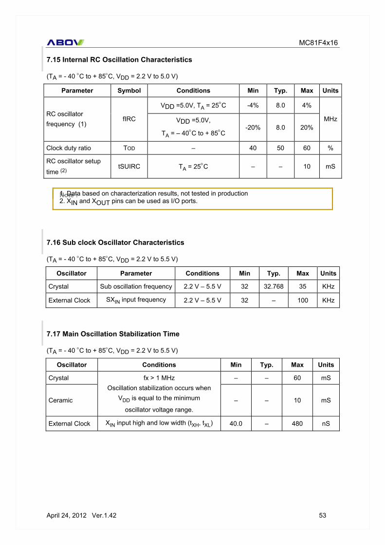
7.15 Internal RC Oscillation Characteristics
(TA = - 40 °C to + 85°C, VDD = 2.2 V to 5.0 V)
Parameter Symbol Conditions Min Typ. Max Units
VDD =5.0V, TA = 25°C -4% 8.0 4% RC oscillator frequency (1)
fIRC VDD =5.0V,
TA = – 40°C to + 85°C -20% 8.0 20%
MHz
Clock duty ratio TOD – 40 50 60 %
RC oscillator setup
time (2) tSUIRC TA = 25°C – – 10 mS
Note : 1. Data based on characterization results, not tested in production 2. XIN and XOUT pins can be used as I/O ports.
7.16 Sub clock Oscillator Characteristics
(TA = - 40 °C to + 85°C, VDD = 2.2 V to 5.5 V)
Oscillator Parameter Conditions Min Typ. Max Units
Crystal Sub oscillation frequency 2.2 V – 5.5 V 32 32.768 35 KHz
External Clock SXIN input frequency 2.2 V – 5.5 V 32 – 100 KHz
7.17 Main Oscillation Stabilization Time
(TA = - 40 °C to + 85°C, VDD = 2.2 V to 5.5 V)
Oscillator Conditions Min Typ. Max Units
Crystal – – 60 mS
Ceramic
fx > 1 MHz Oscillation stabilization occurs when
VDD is equal to the minimum
oscillator voltage range. – – 10 mS
External Clock XIN input high and low width (tXH, tXL) 40.0 – 480 nS
MC81F4x16
54 April 24, 2012 Ver.1.42
XIN 0.8VDD
0.2VDD
tXHtXL
1 / fx
7.18 Sub Oscillation Stabilization Time
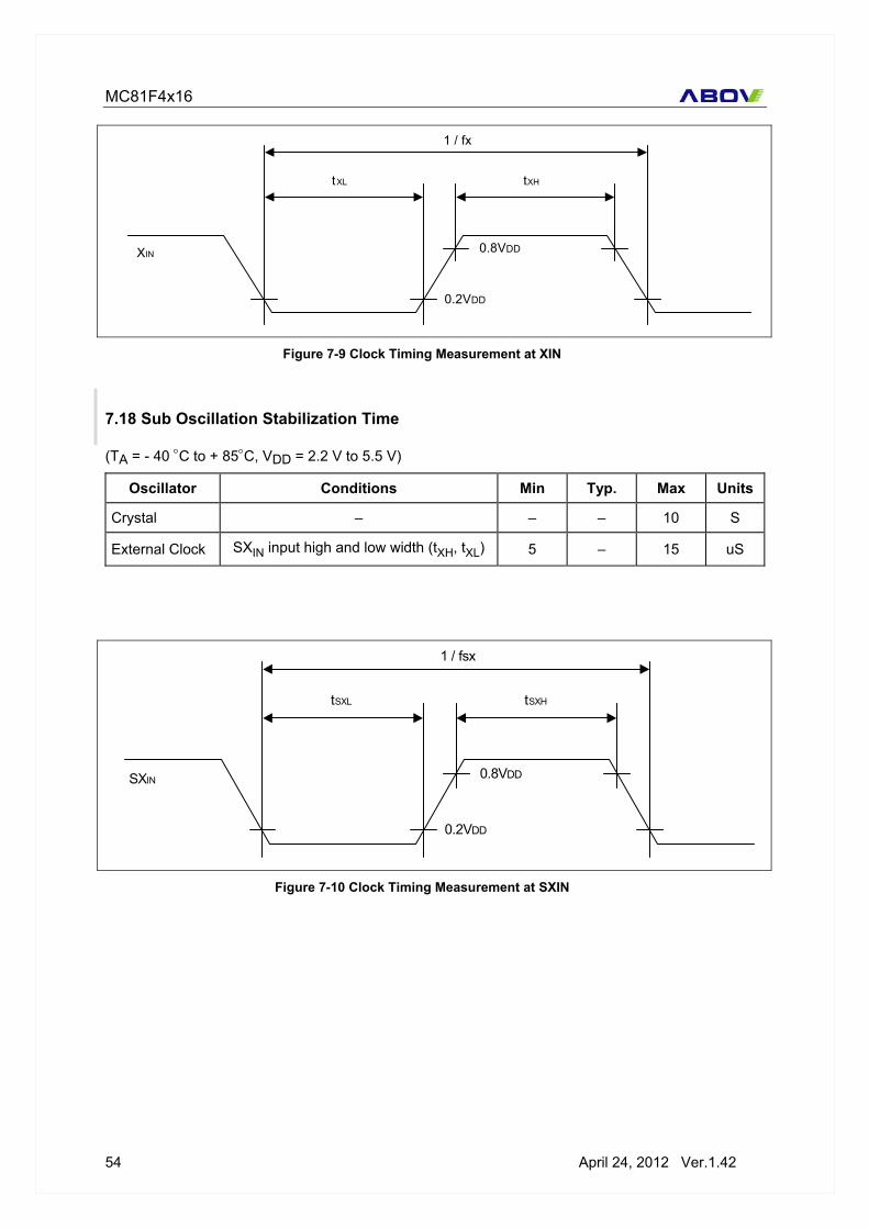
(TA = - 40 °C to + 85°C, VDD = 2.2 V to 5.5 V)
Oscillator Conditions Min Typ. Max Units
Crystal – – – 10 S
External Clock SXIN input high and low width (tXH, tXL) 5 – 15 uS
1 / fsx
SXIN 0.8VDD
0.2VDD
tSXHtSXL
Figure 7-9 Clock Timing Measurement at XIN
Figure 7-10 Clock Timing Measurement at SXIN
MC81F4x16
April 24, 2012 Ver.1.42 55
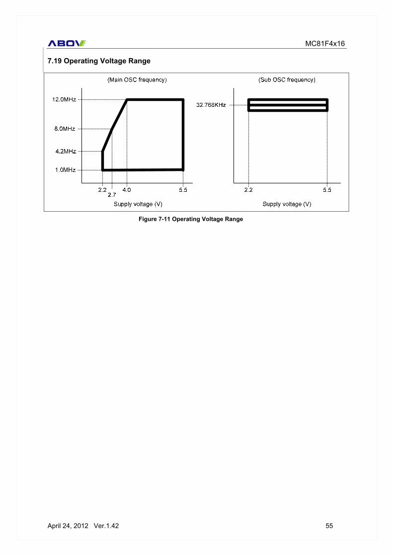
7.19 Operating Voltage Range
Figure 7-11 Operating Voltage Range

MC81F4x16
56 April 24, 2012 Ver.1.42
7.20 Typical Characteristics
These graphs and tables provided in this section are for design guidance only and are not tested or guaranteed. In some graphs or tables the data presented are outside specified operating range (e.g. outside specified VDD range). This is for information only and devices are guaranteed to operate properly only within the specified range. The data presented in this section is a statistical summary of data collected on units from different lots over a period of time. “Typical” represents the mean of the distribution while “max” or “min” represents (mean + 3σ) and (mean − 3σ) respectively where σ is standard deviation.
Figure 7-12 IDD – VDD in Normal Mode
Figure 7-13 ISLEEP – VDD in Sleep Mode
Figure 7-14 IDD2 – VDD in Sub Active Mode
Figure 7-15 ISLEEP2 – VDD with Sub Clock

MC81F4x16
April 24, 2012 Ver.1.42 57
Figure 7-16 ISTOP – VDD in STOP Mode
Figure 7-17 IOH1 - VOH1 at VDD=5v Figure 7-18 IOH2 – VOH2 at VDD=5V

MC81F4x16
58 April 24, 2012 Ver.1.42
Figure 7-19 IOL1 - VOL1 at VDD=5v Figure 7-20 IOL2 - VOL2 at VDD=5v
Figure 7-21 VIH1 - VDD
Figure 7-22 VIL1 - VDD

MC81F4x16
April 24, 2012 Ver.1.42 59
Figure 7-23 VIH2 - VDD
Figure 7-24 VIL2 - VDD
Figure 7-25 VIH3 - VDD
Figure 7-26 VIL3 - VDD

MC81F4x16
60 April 24, 2012 Ver.1.42
Figure 7-27 8MHz Internal OSC Freq. - VDD
Figure 7-28 Ext. R/C OSC Freq. - VDD at 25
Figure 7-29 Ext. R/C OSC Freq. - VDD at 85
Figure 7-30 Ext.l R/C OSC Freq. - VDD at -40

MC81F4x16
April 24, 2012 Ver.1.42 61
8. ROM OPTION The ROM Option is a start-condition byte of the chip. The default ROM Option value is 00H (LVR enable and External RC is selected). It can be changed by appropriate writing tools such as PGMPlusUSB, ISP, etc.
8.1 Rom Option 7 6 5 4 3 2 1 0
LVREN LVRS – – OSCS ROM OPTION
0: Enable (R35) LVREN LVR Enable/Disable bit
1: Disable (RESETB) 00: 2.4V 01: 2.7V 10: 3.0V
LVRS LVR Level Selection bits
11: 4.0V – bit4 – bit3 Not used MC81F4x16
000: External RC 001: Internal RC; 4MHz 010: Internal RC; 2MHz 011: Internal RC; 1MHz 100: Internal RC; 8MHz 101: Not available ( Note 4 ) 110: Not available ( Note 5 )
OSCS Oscillator Selection bits
111: Crystal/ceramic oscillator
Note : 1. When LVR is enabled, LVR level should be set to appropriate value, not default value. 2. When you select the Crystal/ceramic oscillator, R33 and R34 pins are automatically selected for XIN and XOUT mode. 3. When you select the external RC, R34 pin is automatically selected for XIN mode. 4. If OSCS is set by ‘101’, Oscillator works as ‘Internal RC; 4MHz’ mode. 5. If OSCS is set by ‘110’, Oscillator works as ‘Internal RC; 2MHz’ mode.

MC81F4x16
62 April 24, 2012 Ver.1.42
8.2 Read Timing
Rom option is affected 32 mili-second (typically) after VDD cross the POR level. More precisely
saying, the 32 mili-second is the time for 1/2 counting of 1024 divided BIT with 4 MHz internal OSC. After the ROM option is affected, system clock source is changed based on the ROM option. And then, rest 1/2 counting is continued with changed clock source. So, hole stabilization time is variable depend on the clock source.
Before read ROM option
After read ROM option
OSC Stabilization Time
Formula 250ns x 128(BTCR) x 1024(divider)
Period x 128(BTCR) x 1024(divider)
Before + After
Int-RC 4MHz 32 ms 32 ms 64 ms
Int-RC 8MHz 32 ms 16 ms 48 ms
X-tal 12 MHz 32 ms 10.7 ms 42.7 ms
X-tal 16 Mhz 32 ms 8 ms 40 ms
Note that ROM option is affected in OSC stabilization time. So even you change the ROM option by
ISP. It is not affected until system is reset. In other words, you must reset the system after change the ROM option.
Table 8-1 examples of OSC stabilization time
POR Start
Volt
Time Rom option
Read
32 ms
POR level
32 ms @4MHz
OSC. Stabilization
Time
Reset process & Main program
Start
VDD rising curve
Figure 8-1 ROM option read timing diagram

MC81F4x16
April 24, 2012 Ver.1.42 63
9. MEMORY ORGANIZATION This MCU has separated address spaces for the *program memory* and the *data Memory*. The program memory is a ROM which stores a program code. It is not possible to write a data at the program memory while the MCU is running. The Data Memory is a REM which is used by MCU at running time. 9.1 Registers There are few registers which are used for MCU operating.
Accumulator( A Register ) : Accumulator is the 8-bit general purpose register, which is used for accumulating and some data operations such as transfer, temporary saving, and conditional judgment , etc. And it can be used as a part of 16-bit register with Y Register as shown below.
X, Y Registers: In the addressing mode, these are used as a index register. It makes it possible to access at Xth or Yth memory from specific address. It is extremely effective for referencing a subroutine table and a memory table. These registers also have increment, decrement, comparison and data transfer functions, and they can be used as a simple accumulator.
Figure 9-1 Configuration of Registers
Figure 9-2 Configuration of YA 16-bit Registers

MC81F4x16
64 April 24, 2012 Ver.1.42
Stack Pointer: Stack Pointer is an 8-bit register which indicates the current ‘push’ point in the stack area. It is used to push and pop when interrupts or general function call is occurred. Stack Pointer identifies the location in the stack to be accessed (save or restore). Generally, SP is automatically updated when a subroutine call is executed or an interrupt is accepted. However, if it is used in excess of the stack area permitted by the data memory allocating configuration, the user-processed data may be lost. The stack can be located at any position within 100H to 1FFH of the internal data memory. The SP is not initialized by hardware, requiring to write the initial value (the location with which the use of the stack starts) by using the initialization routine. Normally, the initial value of “FFH” is used.
Figure 9-3 Stack Pointer
Figure 9-4 Stack Operation

MC81F4x16
April 24, 2012 Ver.1.42 65
Program Status Word: Program Status Word (PSW)contains several bits that reflect the current state of the CPU. It contains the Negative flag, the Overflow flag, the Break flag the Half Carry (for BCD operation), the Interrupt enable flag, the Zero flag, and the Carry flag. [Carry flag C] This flag stores any carry or borrow from the ALU of CPU after an arithmetic operation and is also changed by the Shift Instruction or Rotate Instruction. [Zero flag Z] This flag is set when the result of an arithmetic operation or data transfer is “0” and is cleared by any other result. [Interrupt disable flag I] This flag enables/disables all interrupts except interrupt caused by Reset or software BRK instruction. All interrupts are disabled when cleared to “0”. This flag immediately becomes “0” when an interrupt is served. It is set by the EI instruction and cleared by the DI instruction. [Half carry flag H] After operation, this is set when there is a carry from bit 3 of ALU or there is no borrow from bit 4 of ALU. This bit can not be set or cleared except CLRV instruction with Overflow flag (V). [Break flag B] This flag is set by software BRK instruction to distinguish BRK from TCALL instruction with the same vector address. [Direct page flag G] This flag assigns RAM page for direct addressing mode. In the direct addressing mode, addressing area is from zero page 00H to 0FFH when this flag is "0". If it is set to "1", addressing area is assigned 100H to 1FFH. It is set by SETG instruction and cleared by CLRG. [Overflow flag V] This flag is set to “1” when an overflow occurs as the result of an arithmetic operation involving signs. An overflow occurs when the result of an addition or subtraction exceeds +127(7FH) or -128(80H). The CLRV instruction clears the overflow flag. There is no set instruction. When the BIT instruction is executed, bit 6 of memory is copied to this flag. [Negative flag N]
Figure 9-5 PSW ( Program Status Word ) Registers

MC81F4x16
66 April 24, 2012 Ver.1.42
This flag is set to match the sign bit (bit 7) status of the result of a data or arithmetic operation. When the BIT instruction is executed, bit 7 of memory is copied to this flag.
9.2 Program Memory
A 16-bit program counter is capable of addressing up to 64K bytes, but this device has 16K bytes program memory space only physically implemented. Accessing a location above FFFFH will cause a wrap-around to 0000H. Figure 9-6 shows a map of Program Memory. After reset, the CPU begins execution from reset vector which is stored in address FFFEH and FFFFH. As shown in Figure 9-6, each area is assigned a fixed location in Program Memory. Program memory area contains the user program Page Call (PCALL) area contains subroutine program to reduce program byte length by using 2 bytes PCALL instead of 3 bytes CALL instruction. If it is frequently called, it is more useful to save program byte length. Table Call (TCALL) causes the CPU to jump to each TCALL address, where it commences the execution of the service routine. The Table Call service area spaces 2-byte for every TCALL: 0FFC0H for TCALL15, 0FFC2H for TCALL14, etc., as shown in Figure 9-7. The interrupt causes the CPU to jump to specific location where it commences the execution of the service routine. The interrupt service locations spaces 2-byte interval. The External interrupt 1, for Example, is
assigned to location 0FFFCH. Any area from 0FF00H to 0FFFFH, if it is not going to be used, its service location is available as general purpose Program Memory.
Figure 9-6 Program Memory Map

MC81F4x16
April 24, 2012 Ver.1.42 67
Figure 9-7 PCALL and TCALL Memory Area

MC81F4x16
68 April 24, 2012 Ver.1.42
Example : Usage of TCALL
LDA #5
TCALL 0FH ;1BYTE INSTRUCTION
: ;INSTEAD OF 3 BYTES
: ;NORMAL CALL
;TABLE CALL ROUTINE
FUNC_A : LDA LRG0
RET
FUNC_B : LDA LRG1
RET
;TABLE CALL ADD. AREA
ORG 0FFC0H ;TCALL ADDRESS AREA
DW FUNC_A
DW FUNC_B

MC81F4x16
April 24, 2012 Ver.1.42 69

MC81F4x16
70 April 24, 2012 Ver.1.42
9.3 Data Memory
Figure 9-8 shows the internal Data Memory space available. Data Memory is divided into three groups, a user RAM, Stack memory and Control registers.
9.4 User Memory
The MC81F4x16 has a 512 bytes user memory (RAM). RAM pages are selected by the RPR register.
RPR RAM PAGE SELECT REGISTER 00E1H
7 6 5 4 3 2 1 0 RPR - RPR bits
R/W R/W R/W R/W R/W R/W R/W R/W Reset value:
----_--00b
00: page 0 01: page 1 RPR bits Ram Page Select bits 10: page 2
Note : After setting RPR(RAM Page Select Register), be sure to execute SETG instruction. Whenever CLRG instruction is excuted, PAGE0 is selected regardless of RPR.
9.5 Stack Area
The stack provides the area where the return address is saved before a jump is performed during the processing routine at the execution of a subroutine call instruction or the acceptance of an interrupt.
Figure 9-8 Data Memory Map

MC81F4x16
April 24, 2012 Ver.1.42 71
When returning from the processing routine, executing the subroutine return instruction [RET] restores the contents of the program counter from the stack; executing the interrupt return instruction [RETI] restores the contents of the program counter and flags. The save/restore locations in the stack are determined by the stack pointed (SP). The SP is automatically decreased after the saving, and increased before the restoring. This means the value of the SP indicates the stack location number for the next save. Refer to Figure 9-4. .
9.6 Control Registers ( SFR )
The control registers are used by the CPU and Peripheral function blocks for controlling the desired operation of the device. Therefore these registers contain control and status bits for the interrupt system, the timer/ counters, analog to digital converters and I/O ports. The control registers are in address range of 0B0H to 0FFH. It also be called by SFR(Special Function Registers). Note that unoccupied addresses may not be implemented on the chip. Read accesses to these addresses will in general return random data, and write accesses will have an indeterminate effect. More detailed information of each registers are explained in each peripheral section. Example : To write at CKCTLR
LDM CKCTLR,#0AH ;Divide ratio(÷32)

MC81F4x16
72 April 24, 2012 Ver.1.42
Initial Value Address Register Name Symbol R/W
7 6 5 4 3 2 1 0 Addressing
Mode
00B0 Timer 0 Status And Control Register T0SCR R/W 0 0 0 0 0 0 0 0 Byte, bit 00B1 Timer 0 Data Register T0DR R/W 1 1 1 1 1 1 1 1 Byte, bit 00B2 Timer 0 Counter Register T0CR R 0 0 0 0 0 0 0 0 Byte, bit 00B3 Timer 1 Status And Control Register T1SCR R/W – 0 0 0 0 0 0 0 Byte, bit 00B4 Timer 1 Data Register T1DR R/W 1 1 1 1 1 1 1 1 Byte, bit 00B5 Timer 1 Counter Register T1CR R 0 0 0 0 0 0 0 0 Byte, bit 00B6 Timer 2 Status And Control Register T2SCR R/W 0 – 0 0 0 0 0 0 Byte, bit 00B7 Timer 2 Data Register T2DR R/W 1 1 1 1 1 1 1 1 Byte, bit 00B8 Timer 2 Counter Register T2CR R 0 0 0 0 0 0 0 0 Byte, bit 00B9 Timer 3 Status And Control Register T3SCR R/W – – 0 0 0 0 0 0 Byte, bit 00BA Timer 3 Data Register T3DR R/W 1 1 1 1 1 1 1 1 Byte, bit 00BB Timer 3 Counter Register T3CR R 0 0 0 0 0 0 0 0 Byte, bit 00BC Oscillator Select Register OSCSEL R/W – – – – – 0 0 0 Byte, bit 00BD A/D Mode Register ADMR R/W 0 0 0 0 0 0 0 0 Byte, bit 00BE A/D Converter Data High Register ADDRH R X X X X X X X X Byte, bit 00BF A/D Converter Data Low Register ADDRL R X X X X – – – – Byte, bit 00C0 R0 Port Data Register R0 R/W 0 0 0 0 0 0 0 0 Byte, bit 00C1 R1 Port Data Register R1 R/W 1 1 1 1 1 0 0 0 Byte, bit 00C2 R2 Port Data Register R2 R/W 1 1 1 1 1 1 1 1 Byte, bit 00C3 R3 Port Data Register R3 R/W – – 0 0 0 1 1 1 Byte, bit 00C4 R4 Port Data Register R4 R/W 1 1 1 1 1 1 1 1 Byte, bit 00C5 R5 Port Data Register R5 R/W – – – – 1 1 1 1 Byte, bit 00C6 R0 Port Control High Register R0CONH R/W 0 0 0 0 0 0 – 0 Byte, bit 00C7 R0 Port Control Middle Register R0CONM R/W 0 0 0 0 0 0 0 0 Byte, bit 00C8 R0 Port Control Low Register R0CONL R/W – – 0 0 0 0 0 0 Byte, bit 00C9 R0 Port Pull-up Enable Register PUR0 R/W 0 0 0 0 0 0 0 0 Byte, bit
00CA R0 Port External Interrupt High Register
EINT0H R/W 0 0 0 0 0 0 0 0 Byte, bit
00CB R0 Port External Interrupt Low Register
EINT0L R/W 0 0 0 0 0 0 0 0 Byte, bit
00CC R0 Port External Interrupt Request Register
ERQ0 R/W 0 0 0 0 0 0 0 0 Byte, bit
00CD External Interrupt Flag Register EINTF R/W 0 0 0 0 0 0 0 0 Byte, bit 00CE PWM Status And Control Register PWMSCR R/W 0 0 0 0 – – – – Byte, bit 00CF PWM Period And Duty Register PWMPDR R/W 1 1 1 1 1 1 1 1 Byte, bit 00D0 PWM2 Data Register PWM2DR R/W 1 1 1 1 1 1 1 1 Byte, bit 00D1 PWM3 Data Register PWM3DR R/W 1 1 1 1 1 1 1 1 Byte, bit 00D2 PWM4 Data Register PWM4DR R/W 1 1 1 1 1 1 1 1 Byte, bit 00D3 R1 Port Control High Register R1CONH R/W 0 1 0 1 0 1 0 1 Byte, bit 00D4 R1 Port Control Middle Register R1CONM R/W 0 0 1 0 0 0 – – Byte, bit 00D5 R1 Port Control Low Register R1CONL R/W – – – 0 0 0 0 0 Byte, bit
Table 9-1 Control Register 1/4

MC81F4x16
April 24, 2012 Ver.1.42 73
Initial Value Address Register Name Symbol R/W
7 6 5 4 3 2 1 0 Addressing
Mode
00D6 R1 Port Pull-up Enable Register PUR1 R/W 0 0 0 0 0 0 0 0 Byte, bit 00D7 R1 Port External Interrupt Register EINT1 R/W 0 0 0 0 0 0 0 0 Byte, bit
00D8 R1 Port External Interrupt Request Register ERQ1 R/W – – – – 0 0 0 0 Byte, bit
00D9 R2 Port Control High Register R2CONH R/W 0 1 0 1 0 1 0 1 Byte, bit 00DA R2 Port Control Low Register R2CONL R/W 0 1 0 1 0 1 0 1 Byte, bit 00DB R2 Port Pull-up Enable Register PUR2 R/W 0 0 0 0 0 0 0 0 Byte, bit 00DC R3 Port Control High Register R3CONH R/W – – 0 0 0 0 0 0 Byte, bit 00DD R3 Port Control Low Register R3CONL R/W 1 0 0 1 1 0 1 1 Byte, bit 00DE R4 Port Control High Register R4CONH R/W 1 0 1 0 1 0 1 0 Byte, bit 00DF R4 Port Control Low Register R4CONL R/W 1 0 1 0 1 0 1 0 Byte, bit 00E0 R5 Port Control Register R5CON R/W 1 0 1 0 1 0 1 0 Byte, bit 00E1 RAM Page Selection Register RPR R/W – – – – – – 0 0 Byte, bit
00E2 Slave IIC Status And Control Register
IICSCR R/W 0 0 0 0 0 0 0 0 Byte, bit
00E3 Slave IIC Address Register IICAR R/W X X X X X X X – Byte, bit 00E4 Slave IIC Data Shift Register IICDSR R/W X X X X X X X X Byte, bit 00E5 Buzzer Control Register BUZR R/W 1 1 0 0 – – – – Byte, bit 00E6 Buzzer Period Data Register BUPDR R/W 1 1 1 1 1 1 1 1 Byte, bit 00E7 SIO Control Register SIOCR R/W – – 0 0 0 0 0 0 Byte, bit 00E8 SIO Data Register SIODAT R/W 0 0 0 0 0 0 0 0 Byte, bit 00E9 SIO Pre-scaler Register SIOPS R/W 0 0 0 0 0 0 0 0 Byte, bit 00EA Interrupt Enable High Register IENH R/W 0 0 0 0 0 0 0 0 Byte, bit 00EB Interrupt Enable Low Register IENL R/W 0 0 0 0 0 0 – 0 Byte, bit 00EC Interrupt Request High Register IRQH R/W 0 0 0 0 0 0 0 0 Byte, bit 00ED Interrupt Request Low Register IRQL R/W 0 0 0 0 0 0 – 0 Byte, bit 00EE Interrupt Flag High Register INTFH R/W 0 0 0 0 0 0 0 0 Byte, bit 00EF Interrupt Flag Low Register INTFL R/W 0 – – – – – 0 0 Byte, bit
00F0 Watch Timer Status And Control Register
WTSCR R/W – 0 0 0 0 – – 0 Byte, bit
00F1 Basic Timer Counter Register BTCR R X X X X X X X X Byte, bit 00F2 Clock control Register CKCTLR R/W – – – 1 0 1 1 1 Byte, bit 00F3 Power On Reset Control Register PORC R/W 0 0 0 0 0 0 0 0 Byte, bit 00F4 Watchdog Timer Register WDTR R/W 0 1 1 1 1 1 1 1 Byte, bit
00F5 Stop & Sleep Mode Control Register
SSCR R/W 0 0 0 0 0 0 0 0 Byte, bit
00F6 Watchdog Timer Status Register WDTSR R/W 0 0 0 0 0 0 0 0 Byte, bit
00F7 Watchdog Timer Counter Register
WDTCR R X X X X X X X X Byte, bit
00FC UART Control High Register UCONH R/W 0 0 0 0 0 0 – – Byte, bit 00FD UART Control Low Register UCONL R/W 0 0 0 0 0 0 – – Byte, bit 00FE UART Data Register UDAT R/W X X X X X X X X Byte, bit 00FF UART Baud Rate Data Register BRDAT R/W 1 1 1 1 1 1 1 1 Byte, bit
Table 9-2 Control Register 2/4

MC81F4x16
74 April 24, 2012 Ver.1.42
Address Name Bit 7 Bit 6 Bit 5 Bit 4 Bit 3 Bit 2 Bit 1 Bit 0
00B0H T0SCR T0MOD T0MS T0CC T0CS 00B1H T0DR Timer 0 Data Register 00B2H T0CR Timer 0 Counter Register 00B3H T1SCR – T1MS T1CC T1CS 00B4H T1DR Timer 1 Data Register 00B5H T1CR Timer 1 Counter Register 00B6H T2SCR T2MOD – T2MS T2CC T2CS 00B7H T2DR Timer 2 Data Register 00B8H T2CR Timer 2 Counter Register 00B9H T3SCR – – T3MS T3CC T3CS 00BAH T3DR Timer 3 Data Register 00BBH T3CR Timer 3 Counter Register 00BCH OSCSEL – – – – – MOSC SOSC SCLK 00BDH ADMR SSBIT EOC ADCLK ADCH 00BEH ADDRH A/D Converter Data High Register 00BFH ADDRL A/D Converter Data Low Register 00C0H R0 R0 Port Data Register 00C1H R1 R1 Port Data Register 00C2H R2 R2 Port Data Register 00C3H R3 R3 Port Data Register 00C4H R4 R4 Port Data Register 00C5H R5 R5 Port Data Register 00C6H R0CONH R07 R06 – R05 00C7H R0CONM R05 R04 R03 00C8H R0CONL – – R02 R01 R00 00C9H PUR0 PUR07 PUR06 PUR05 PUR04 PUR03 PUR02 PUR01 PUR0000CAH EINT0H EXT5IE EXT4IE EXT3IE EXT2IE 00CBH EINT0L EXT1IE EXT0IE EXT11IE EXT10IE 00CCH ERQ0 EXT5IR EXT4IR EXT3IR EXT2IR EXT1IR EXT0IR EXT11IR EXT10IR00CDH EINTF EXT0IF EXT2IF EXT4IF EXT7IF EXT8IF EXT9IF EXT10IF EXT11IF00CEH PWMSCR POL4 POL3 POL2 PWMS – – – – 00CFH PWMPDR P4DH P4DL P3DH P3DL P2DH P2DL PPH PPL 00D0H PWM2DR PWM 2 Data Register 00D1H PWM3DR PWM 3 Data Register 00D2H PWM4DR PWM 4 Data Register 00D3H R1CONH R17 R16 R15 R14 00D4H R1CONM R13 R12 – – 00D5H R1CONL – – – R11 R10
Table 9-3 Control Register 3/4

MC81F4x16
April 24, 2012 Ver.1.42 75
Address Name Bit 7 Bit 6 Bit 5 Bit 4 Bit 3 Bit 2 Bit 1 Bit 0
00D6H PUR1 PUR17 PUR16 PUR15 PUR14 PUR13 PUR12 PUR11 PUR1000D7H EINT1 EXT9IE EXT8IE EXT7IE EXT6IE 00D8H ERQ1 – – – – EXT9IR EXT8IR EXT7IR EXT6IR00D9H R2CONH R27 R26 R25 R24 00DAH R2CONL R23 R22 R21 R20 00DBH PUR2 PUR27 PUR26 PUR25 PUR24 PUR23 PUR22 PUR21 PUR2000DCH R3CONH – – R35 R34 R33 00DDH R3CONL R32 R31 R30 00DEH R4CONH R47 R46 R45 R44 00DFH R4CONL R43 R42 R41 R40 00E0H R5CON R53 R52 R51 R50 00E1H RPR – – – – – – RPR1 RPR0 00E2H IICSCR ACKE IICEN IICIFEN IICAZS IICTR IICBS SAM IICLR 00E3H IICAR Slave IIC Address register 00E4H IICDSR Slave IIC Tx/Rx Data Shift Register 00E5H BUZR BUCK BUSS BURL – – – – 00E6H BUPDR Buzzer Period Data Register 00E7H SIOCR – – CSEL DAT SIOM SIOP CCLR SEDGE00E8H SIODAT SIO Data register 00E9H SIOPS SIO Pre-Scale register 00EAH IENH T0MIE T0OVIE T1MIE T1OVIE T2MIE T2OVIE T3MIE T3OVIE00EBH IENL IICIE SIOIE WTIE URIE UTIE WDTIE – BTIE 00ECH IRQH T0MIR T0OVIR T1MIR T1OVIR T2MIR T2OVIR T3MIR T3OVIR00EDH IRQL IICIR SIOIR WTIR URIR UTIR WDTIR – BTIR 00EEH INTFH T0MIF T0OVIF T1MIF T1OVIF T2MIF T2OVIF T3MIF T3OVIF00EFH INTFL IICIF – – – – – URIF UTIF 00F0H WTSCR – WTEN WTSS – – WTCS00F1H BTCR Basic Timer Counter Register 00F2H CKCTLR – – – WDTON BTCL BTS 00F3H PORC Power On Reset Control register 00F4H WDTR WDTCL WDTCMP 00F5H SSCR Stop and Sleep Control Register 00F6H WDTSR Watchdog Timer Status Register 00F7H WDTCR Watchdog Timer Counter Register 00FCH UCONH UMS1 UMS0 MCE SDR TB8 RB8 – – 00FDH UCONL UTP UTPS URPS URPER UCLK – – 00FEH UDAT UART Data Register 00FFH BRDAT UART Baud Rate Register
Table 9-4 Control Register 4/4

MC81F4x16
76 April 24, 2012 Ver.1.42
9.7 Addressing modes
The MC81Fxxxx series MCU uses six addressing modes;
- Register Addressing - Immediate Addressing - Direct Page Addressing - Absolute Addressing - Indexed Addressing - Indirect Addressing
Register Addressing Register addressing means to access to the data of the A, X, Y, C and PSW registers. For Example ‘ASL ( Arithmetic Shift Left )’ only accesses the A register.
Immediate Addressing In this mode, second byte (operand) is accessed as a data immediately. Example :
:
ADC #35h ;op code is 04h
:
:
When G-flag is 1, then RAM address is defined by 16-bit address which is composed of 8-bit RAM paging register (RPR) and 8-bit immediate data. Example :
: ;When G = 1, RPR = 1
LDM #35h,#55h ;op code is 0E4h
:
:

MC81F4x16
April 24, 2012 Ver.1.42 77
Direct Page Addressing -> dp In this mode, an address is specified within direct page. Current accessed page is selected by RPR(RAM Page select Register). And dp( Direct Page ) is an one byte data which indicates the target address in the current accessed page. Example :
: ;When G = 0
LDA 35h ;A = [35h]
: ;op code is 0C5h
:
Absolute Addressing Absolute addressing sets corresponding memory data to Data, i.e. second byte (Operand I) of command becomes lower level address and third byte (Operand II) becomes upper level address. With 3 bytes command, it is possible to access to whole memory area. ADC, AND, CMP, CMPX, CMPY, EOR, LDA, LDX,LDY, OR, SBC, STA, STX, STY The operation within data memory (RAM) : ASL, BIT, DEC, INC, LSR, ROL, ROR Example :
: ;When G = 0
ADC !0F035h ;A = A + C + ROM[0F035h]
: ;op code is 07h
:

MC81F4x16
78 April 24, 2012 Ver.1.42
Example : Addressing accesses the address 0135H regardless of G-flag.
: ;When G = 0
INC !0135h ;increase ROM[135h]
: ;op code is 98h
:
Indexed Addressing X indexed direct page (no offset) → X In this mode, an address is specified by the X register. ADC, AND, CMP, EOR, LDA, OR, SBC, STA, XMA Example :
: ;When G = 1, X = 15h
LDA X ;A = ROM[(RPR<<8) + X]
: ;op code is 0D4h
:
X indexed direct page, auto increment→ X+ In this mode, a address is specified within direct page by the X register and the content of X is increased by 1. LDA, STA

MC81F4x16
April 24, 2012 Ver.1.42 79
Example:
: ;When G = 0, X = 35h
LDA X+ ;A = ROM[(RPR<<8) + X]
: ; and X = X + 1
: ;op code is 0DBh
:
X indexed direct page (8 bit offset) → dp+X This address value is the second byte (Operand) of command plus the data of X-register. And it assigns the memory in direct page. ADC, AND, CMP, EOR, LDA, LDY, OR, SBC, STA,STY, XMA, ASL, DEC, INC, LSR, ROL, ROR Example :
: ;When G = 0, X = 0F5h
LDA 45h + X ;op code is 0C6h
: ;
: ;
:
Y indexed direct page (8 bit offset) → dp+Y This address value is the second byte (Operand) of command plus the data of Y-register, which assigns Memory in Direct page. This is same with above ‘X indexed direct page’. Use Y register instead of X.

MC81F4x16
80 April 24, 2012 Ver.1.42
Y indexed absolute → !abs+Y Accessing the value of 16-bit absolute address plus Y-register value. This addressing mode can specify memory in whole area. Example :
: ;when Y = 55h
LDA !0FA00H+Y ;op code is D5h
:
Indirect Addressing Direct page indirect → [dp] Assigns data address to use for accomplishing command which sets memory data (or pair memory) by Operand. Also index can be used with Index register X,Y. JMP, CALL Example :
: ;when G = 0
JMP [35h] ;op code is 3Fh
:

MC81F4x16
April 24, 2012 Ver.1.42 81
X indexed indirect → [dp+X] Processes memory data as Data, assigned by 16-bit pair memory which i s determined by pair data [dp+X+1][dp+X] Operand plus X-register data in Direct page. ADC, AND, CMP, EOR, LDA, OR, SBC, STA Example :
: ;when G = 0
: ; X = 10h
ADC [25h + X] ;op code is 16h
:
Y indexed indirect → [dp]+Y Processes memory data as Data, assigned by the data [dp+1][dp] of 16-bit pair memory paired by Operand in Direct page plus Y-register data. ADC, AND, CMP, EOR, LDA, OR, SBC, STA Example :
: ;when G = 0
: ; Y = 10h
ADC [25h + Y] ;op code is 17h
:

MC81F4x16
82 April 24, 2012 Ver.1.42
Absolute indirect → [!abs] The program jumps to address specified by 16-bit absolute address. JMP Example :
: ;when G = 0
JMP [0E025h] ;op code is 1Fh
:

MC81F4x16
April 24, 2012 Ver.1.42 83
10. I/O PORTS The MC81F4x16 microcontroller has six I/O ports, P0-P5. The CPU accesses ports by writing or reading port register directly.
The R0 port has following features, - 1-bit programmable I/O port.
- Schmitt trigger input, push-pull or open-drain output mode can be selected by software.
- A pull-up resistor can be specified in 1-bit.
- R00-R01 can be used as EXT10/SXin, EXT11/SXout
- R02-R07 can be used as EXT0-EXT5/AD0-AD5
- R02-R03 can be used as EC0, T0O/T0PWM
- R04-R05 can be used as EC1/SCK, T1O/T1PWM/SI
- R06-R07 can be used as EC2/SO, T2O
The R1 port has following features,
- 1-bit programmable I/O port.
- Schmitt trigger input, push-pull or open-drain output mode can be selected by software.
- A pull-up resistor can be specified in 1-bit.
- R10-R13 can be used as EXT6-EXT9/Vref, AN6-AN8
- R11-R13 can be used as PWM2O-PWM4O
- R12 can be used as BUZO
- R14-R17 can be used as RxD, TxD, SDA, SCL
The R2 port has following features,
- 1-bit programmable I/O port.
- Input, push-pull or open-drain output mode can be selected by software.
- A pull-up resistor can be specified in 1-bit.
- R20 can be used as AN9
- R25-R27 can be used as AN10-AN12

MC81F4x16
84 April 24, 2012 Ver.1.42
The R3 port has following features, - 1-bit programmable I/O port.
- Schmitt trigger or normal input, push-pull or open-drain output mode can be selected by software.
- R30-R31 can be used as AN13-AN14
- R33-R34 can be used as Xout, Xin
- R35 can be used as RESETB
The R4 port has following features, - 1-bit programmable I/O port.
- Input, push-pull or open-drain output mode can be selected by software.
The R5 port has following features, - 1-bit programmable I/O port.
- Input, push-pull or open-drain output mode can be selected by software.
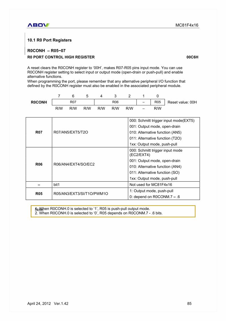
MC81F4x16
April 24, 2012 Ver.1.42 85
10.1 R0 Port Registers
R0CONH – R05~07 R0 PORT CONTROL HIGH REGISTER 00C6H A reset clears the R0CONH register to ‘00H’, makes R07-R05 pins input mode. You can use R0CONH register setting to select input or output mode (open-drain or push-pull) and enable alternative functions. When programming the port, please remember that any alternative peripheral I/O function that defined by the R0CONH register must also be enabled in the associated peripheral module.
7 6 5 4 3 2 1 0 R0CONH R07 R06 – R05 Reset value: 00H
R/W R/W R/W R/W R/W R/W – R/W
000: Schmitt trigger input mode(EXT5) 001: Output mode, open-drain 010: Alternative function (AN5) 011: Alternative function (T2O)
R07 R07/AN5/EXT5/T2O
1xx: Output mode, push-pull 000: Schmitt trigger input mode (EC2/EXT4) 001: Output mode, open-drain 010: Alternative function (AN4) 011: Alternative function (SO)
R06 R06/AN4/EXT4/SO/EC2
1xx: Output mode, push-pull – bit1 Not used for MC81F4x16
1: Output mode, push-pull R05 R05/AN3/EXT3/SI/T1O/PWM1O
0: depend on R0CONM.7 – .6
Note: 1. When R0CONH.0 is selected to ‘1’, R05 is push-pull output mode. 2. When R0CONH.0 is selected to ‘0’, R05 depends on R0CONM.7 - .6 bits.

MC81F4x16
86 April 24, 2012 Ver.1.42
R0CONM – R03~05 R0 PORT CONTROL MIDDLE REGISTER 00C7H A reset clears the R0CONM register to ‘00H’, makes R04-R03 pins input mode. You can use R0CONM register setting to select input or output mode (open-drain or push-pull) and enable alternative functions. When programming the port, please remember that any alternative peripheral I/O function that defined by the R0CONM register must also be enabled in the associated peripheral module.
7 6 5 4 3 2 1 0 R0CONM R05 R04 R03 Reset value: 00H
R/W R/W R/W R/W R/W R/W R/W R/W
00: Schmitt trigger input mode (SI/EXT3)01: Output mode, open-drain 10: Alternative function (AN3)
R05 R05/AN3/EXT3/SI/T1O/PWM1O
11: Alternative function (T1O/PWM1O) 000: Schmitt trigger input mode ( *SCK in / EC1 / EXT2) 001: Output mode, open-drain 010: Alternative function (AN2) 011: Alternative function (SCK out)
R04 R04/AN2/EXT2/SCK/EC1
1xx: Output mode, push-pull 000: Schmitt trigger input mode(EXT1) 001: Output mode, open-drain 010: Alternative function (AN1) 011: Alternative function (T0O/PWM0O)
R03 R03/AN1/EXT1/T0O/PWM0O
1xx: Output mode, push-pull
Note: If you want to use SIO module in slave mode, you must set SCK port as an input mode.
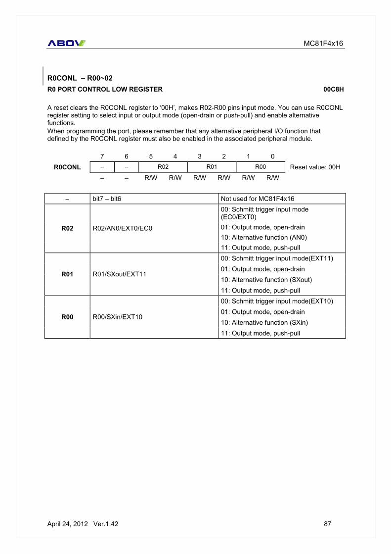
MC81F4x16
April 24, 2012 Ver.1.42 87
R0CONL – R00~02 R0 PORT CONTROL LOW REGISTER 00C8H A reset clears the R0CONL register to ‘00H’, makes R02-R00 pins input mode. You can use R0CONL register setting to select input or output mode (open-drain or push-pull) and enable alternative functions. When programming the port, please remember that any alternative peripheral I/O function that defined by the R0CONL register must also be enabled in the associated peripheral module.
7 6 5 4 3 2 1 0 R0CONL – – R02 R01 R00 Reset value: 00H
– – R/W R/W R/W R/W R/W R/W
– bit7 – bit6 Not used for MC81F4x16 00: Schmitt trigger input mode (EC0/EXT0) 01: Output mode, open-drain 10: Alternative function (AN0)
R02 R02/AN0/EXT0/EC0
11: Output mode, push-pull 00: Schmitt trigger input mode(EXT11) 01: Output mode, open-drain 10: Alternative function (SXout)
R01 R01/SXout/EXT11
11: Output mode, push-pull 00: Schmitt trigger input mode(EXT10) 01: Output mode, open-drain 10: Alternative function (SXin)
R00 R00/SXin/EXT10
11: Output mode, push-pull

MC81F4x16
88 April 24, 2012 Ver.1.42
PUR0 R0 PORT PULL-UP ENABLE REGISTER 00C9H Using the PUR0 register, you can configure pull-up resistors to individual R07-R00 pins.
7 6 5 4 3 2 1 0 PUR0 PUR07 PUR06 PUR05 PUR04 PUR03 PUR02 PUR01 PUR00 Reset value: 00H
R/W R/W R/W R/W R/W R/W R/W R/W
0: Disable pull-up resistor PUR07 R07 Pull-up Resistor Enable Bit
1: Enable pull-up resistor 0: Disable pull-up resistor
PUR06 R06 Pull-up Resistor Enable Bit 1: Enable pull-up resistor 0: Disable pull-up resistor
PUR05 R05 Pull-up Resistor Enable Bit 1: Enable pull-up resistor 0: Disable pull-up resistor
PUR04 R04 Pull-up Resistor Enable Bit 1: Enable pull-up resistor 0: Disable pull-up resistor
PUR03 R03 Pull-up Resistor Enable Bit 1: Enable pull-up resistor 0: Disable pull-up resistor
PUR02 R02 Pull-up Resistor Enable Bit 1: Enable pull-up resistor 0: Disable pull-up resistor
PUR01 R01 Pull-up Resistor Enable Bit 1: Enable pull-up resistor 0: Disable pull-up resistor
PUR00 R00 Pull-up Resistor Enable Bit 1: Enable pull-up resistor
R0 R0 PORT DATA REGISTER 00C0H
7 6 5 4 3 2 1 0 R0 R07 R06 R05 R04 R03 R02 R01 R00 Reset value: 00H
R/W R/W R/W R/W R/W R/W R/W R/W
In input mode, it represents the R0 port status. In output mode, R0 port represents it.
1: High 0 : Low

MC81F4x16
April 24, 2012 Ver.1.42 89
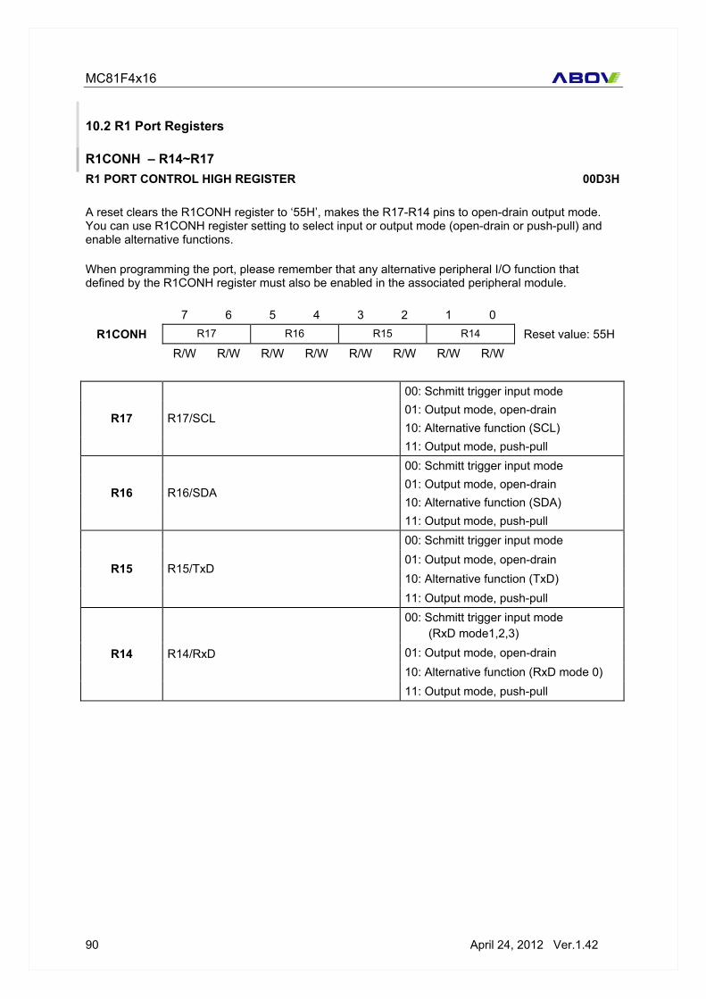
MC81F4x16
90 April 24, 2012 Ver.1.42
10.2 R1 Port Registers
R1CONH – R14~R17 R1 PORT CONTROL HIGH REGISTER 00D3H A reset clears the R1CONH register to ‘55H’, makes the R17-R14 pins to open-drain output mode. You can use R1CONH register setting to select input or output mode (open-drain or push-pull) and enable alternative functions. When programming the port, please remember that any alternative peripheral I/O function that defined by the R1CONH register must also be enabled in the associated peripheral module.
7 6 5 4 3 2 1 0 R1CONH R17 R16 R15 R14 Reset value: 55H
R/W R/W R/W R/W R/W R/W R/W R/W
00: Schmitt trigger input mode 01: Output mode, open-drain 10: Alternative function (SCL)
R17 R17/SCL
11: Output mode, push-pull 00: Schmitt trigger input mode 01: Output mode, open-drain 10: Alternative function (SDA)
R16 R16/SDA
11: Output mode, push-pull 00: Schmitt trigger input mode 01: Output mode, open-drain 10: Alternative function (TxD)
R15 R15/TxD
11: Output mode, push-pull 00: Schmitt trigger input mode
(RxD mode1,2,3) 01: Output mode, open-drain 10: Alternative function (RxD mode 0)
R14 R14/RxD
11: Output mode, push-pull

MC81F4x16
April 24, 2012 Ver.1.42 91
R1CONM – R12~R13 R1 PORT CONTROL MIDDLE REGISTER 00D4H A reset clears the R1CONM register to ‘20H’, makes the R13 pin to open-drain output mode and the R12 pin to input mode. You can use R1CONM register setting to select input or output mode (open-drain or push-pull) and enable alternative functions. When programming the port, please remember that any alternative peripheral I/O function that defined by the R1CONM register must also be enabled in the associated peripheral module.
7 6 5 4 3 2 1 0 R1CONM R13 R12 – – Reset value: 20H
R/W R/W R/W R/W R/W R/W – –
000: Schmitt trigger input mode(EXT9) 001: Output mode, open-drain 010: Alternative function (AN8) 011: Alternative function (PWM4O)
R13 R13/AN8/EXT9/PWM4O
1xx: Output mode, push-pull 000: Schmitt trigger input mode(EXT8) 001: Output mode, open-drain 010: Alternative function (AN7) 011: Alternative function (PWM3O) 101: Alternative function (BUZO) 111: Output mode, push-pull
R12 R12/AN7/EXT8/PWM3O/BUZO
Others: Not available – bit1 – bit0 Not used for MC81F4x16

MC81F4x16
92 April 24, 2012 Ver.1.42
R1CONL – R10~11 R1 PORT CONTROL LOW REGISTER 00D5H A reset clears the R1CONL register to ‘00H’, makes R11-R10 pins input mode. You can use R1CONL register setting to select input or output mode (open-drain or push-pull) and enable alternative functions. When programming the port, please remember that any alternative peripheral I/O function that defined by the R1CONL register must also be enabled in the associated peripheral module.
7 6 5 4 3 2 1 0 R1CONL – – – R11 R10 Reset value: 00H
– – – R/W R/W R/W R/W R/W
– bit7 – bit5 Not used for MC81F4x16 000: Schmitt trigger input mode(EXT7) 001: Output mode, open-drain 010: Alternative function (AN6) 011: Alternative function (PWM2O)
R11 R11/AN6/EXT7/PWM2O
1xx: Output mode, push-pull 00: Schmitt trigger input mode(EXT6) 01: Output mode, open-drain 10: Alternative function (Vref)
R10 R10/Vref/EXT6
11: Output mode, push-pull

MC81F4x16
April 24, 2012 Ver.1.42 93
PUR1 R1 PORT PULL-UP ENABLE REGISTER 00D6H Using the PUR1 register, you can configure pull-up resistors to individual R17-R10 pins.
7 6 5 4 3 2 1 0 PUR1 PUR17 PUR16 PUR15 PUR14 PUR13 PUR12 PUR11 PUR10 Reset value: 00H
R/W R/W R/W R/W R/W R/W R/W R/W
0: Disable pull-up resistor PUR17 R17 Pull-up Resistor Enable Bit
1: Enable pull-up resistor 0: Disable pull-up resistor
PUR16 R16 Pull-up Resistor Enable Bit 1: Enable pull-up resistor 0: Disable pull-up resistor
PUR15 R15 Pull-up Resistor Enable Bit 1: Enable pull-up resistor 0: Disable pull-up resistor
PUR14 R14 Pull-up Resistor Enable Bit 1: Enable pull-up resistor 0: Disable pull-up resistor
PUR13 R13 Pull-up Resistor Enable Bit 1: Enable pull-up resistor 0: Disable pull-up resistor
PUR12 R12 Pull-up Resistor Enable Bit 1: Enable pull-up resistor 0: Disable pull-up resistor
PUR11 R11 Pull-up Resistor Enable Bit 1: Enable pull-up resistor 0: Disable pull-up resistor
PUR10 R10 Pull-up Resistor Enable Bit 1: Enable pull-up resistor
R1 R1 PORT DATA REGISTER 00C1H
7 6 5 4 3 2 1 0 R1 R17 R16 R15 R14 R13 R12 R11 R10 Reset value: F8H
R/W R/W R/W R/W R/W R/W R/W R/W
In input mode, it represents the R1 port status. In output mode, R1 port represents it.
1: High 0 : Low

MC81F4x16
94 April 24, 2012 Ver.1.42
10.3 R2 Port Registers
R2CONH – R24~R27 R2 PORT CONTROL HIGH REGISTER 00D9H A reset clears the R2CONH register to ‘55H’, makes the R27-R24 pins to open-drain output mode. You can use R2CONH register setting to select input or output mode (open-drain or push-pull) and enable alternative functions. When programming the port, please remember that any alternative peripheral I/O function that defined by the R2CONH register must also be enabled in the associated peripheral module.
7 6 5 4 3 2 1 0
R2CONH R27 R26 R25 R24 Reset value: 55H
R/W R/W R/W R/W R/W R/W R/W R/W
00: Input mode
01: Output mode, open-drain
10: Alternative function (AN12) R27 R27/AN12
11: Output mode, push-pull
00: Input mode
01: Output mode, open-drain
10: Alternative function (AN11) R26 R26/AN11
11: Output mode, push-pull
00: Input mode
01: Output mode, open-drain
10: Alternative function (AN10) R25 R25/AN10
11: Output mode, push-pull
00: Input mode
01: Output mode, open-drain
10: Not available R24 R24
11: Output mode, push-pull

MC81F4x16
April 24, 2012 Ver.1.42 95
R2CONL – R20~R23 R2 PORT CONTROL LOW REGISTER 00DAH A reset clears the R2CONL register to ‘55H’, makes R23-R20 pins to open-drain output mode. You can use R2CONL register setting to select input or output mode (open-drain or push-pull) and enable alternative functions. When programming the port, please remember that any alternative peripheral I/O function that defined by the R2CONL register must also be enabled in the associated peripheral module.
7 6 5 4 3 2 1 0
R2CONL R23 R22 R21 R20 Reset value: 55H
R/W R/W R/W R/W R/W R/W R/W R/W
00: Input mode
01: Output mode, open-drain
10: Not available R23 R23
11: Output mode, push-pull
00: Input mode
01: Output mode, open-drain
10: Not available R22 R22
11: Output mode, push-pull
00: Input mode
01: Output mode, open-drain
10: Not available R21 R21
11: Output mode, push-pull
00: Input mode
01: Output mode, open-drain
10: Alternative function (AN9) R20 R20/AN9
11: Output mode, push-pull

MC81F4x16
96 April 24, 2012 Ver.1.42
PUR2 R2 PORT PULL-UP ENABLE REGISTER 00DBH Using the PUR2 register, you can configure pull-up resistors to individual R27-R20 pins.
7 6 5 4 3 2 1 0 PUR2 PUR27 PUR26 PUR25 PUR24 PUR23 PUR22 PUR21 PUR20 Reset value: 00H
R/W R/W R/W R/W R/W R/W R/W R/W
0: Disable pull-up resistor PUR27 R27 Pull-up Resistor Enable Bit
1: Enable pull-up resistor 0: Disable pull-up resistor
PUR26 R26 Pull-up Resistor Enable Bit 1: Enable pull-up resistor 0: Disable pull-up resistor
PUR25 R25 Pull-up Resistor Enable Bit 1: Enable pull-up resistor 0: Disable pull-up resistor
PUR24 R24 Pull-up Resistor Enable Bit 1: Enable pull-up resistor 0: Disable pull-up resistor
PUR23 R23 Pull-up Resistor Enable Bit 1: Enable pull-up resistor 0: Disable pull-up resistor
PUR22 R22 Pull-up Resistor Enable Bit 1: Enable pull-up resistor 0: Disable pull-up resistor
PUR21 R21 Pull-up Resistor Enable Bit 1: Enable pull-up resistor 0: Disable pull-up resistor
PUR20 R20 Pull-up Resistor Enable Bit 1: Enable pull-up resistor
R2 R2 PORT DATA REGISTER 00C2H
7 6 5 4 3 2 1 0 R2 R27 R26 R25 R24 R23 R22 R21 R20 Reset value: FFH
R/W R/W R/W R/W R/W R/W R/W R/W
In input mode, it represents the R2 port status. In output mode, R2 port represents it.
1: High 0 : Low

MC81F4x16
April 24, 2012 Ver.1.42 97
10.4 R3 Port Registers
R3CONH – R33~R35 R3 PORT CONTROL HIGH REGISTER 00DCH A reset clears the R3CONH register to ‘00H’, makes R35-R33 pins input mode. You can use R3CONH register setting to select input or output mode (open-drain or push-pull) and enable alternative functions.
7 6 5 4 3 2 1 0 R3CONH – – R35 R34 R33 Reset value: 00H
– – R/W R/W R/W R/W R/W R/W
– bit7 – bit6 Not used for MC81F4x16 00: Schmitt trigger input mode 01: Not available 10: Output mode, open-drain
R35 R35/RESETB ( *note* )
11: Not available 00: Schmitt trigger input mode 01: Schmitt trigger input pull-up mode 10: Output mode, open-drain
R34 R34/Xin ( *note* )
11: Output mode, push-pull 00: Schmitt trigger input mode 01: Schmitt trigger input pull-up mode 10: Output mode, open-drain
R33 R33/Xout ( *note* )
11: Output mode, push-pull
Note : If you want to use RESETB, the LVREN (ROM OPTION [7]) must select to LVR disable mode (‘1’). If you want to use R35, the LVREN (ROM OPTION [7]) must be selected to LVR enable mode (‘0’). If you want to use XIN and XOUT, the OSCS (ROM OPTION [2:0]) must select to Crystal/ceramic oscillator mode (111b). If you want to use R33 and R34, the OSCS (ROM OPTION [2:0]) must select to Internal RC mode (001b, 010b, 011b, 100b). Even you are in case of using emulator you must select the ROM OPTION switch properly to use those R33,R34,R35 ports.
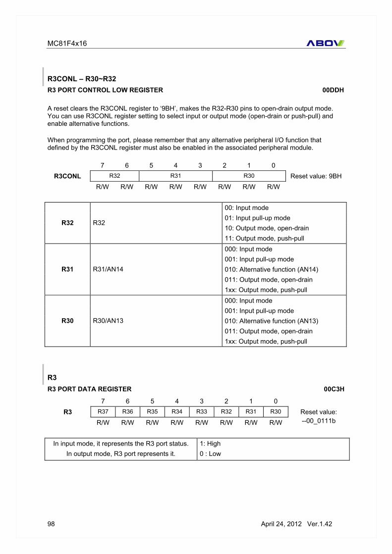
MC81F4x16
98 April 24, 2012 Ver.1.42
R3CONL – R30~R32 R3 PORT CONTROL LOW REGISTER 00DDH A reset clears the R3CONL register to ‘9BH’, makes the R32-R30 pins to open-drain output mode. You can use R3CONL register setting to select input or output mode (open-drain or push-pull) and enable alternative functions. When programming the port, please remember that any alternative peripheral I/O function that defined by the R3CONL register must also be enabled in the associated peripheral module.
7 6 5 4 3 2 1 0 R3CONL R32 R31 R30 Reset value: 9BH
R/W R/W R/W R/W R/W R/W R/W R/W
00: Input mode 01: Input pull-up mode 10: Output mode, open-drain
R32 R32
11: Output mode, push-pull 000: Input mode 001: Input pull-up mode 010: Alternative function (AN14) 011: Output mode, open-drain
R31 R31/AN14
1xx: Output mode, push-pull 000: Input mode 001: Input pull-up mode 010: Alternative function (AN13) 011: Output mode, open-drain
R30 R30/AN13
1xx: Output mode, push-pull
R3 R3 PORT DATA REGISTER 00C3H
7 6 5 4 3 2 1 0 R3 R37 R36 R35 R34 R33 R32 R31 R30
R/W R/W R/W R/W R/W R/W R/W R/W Reset value: --00_0111b
In input mode, it represents the R3 port status.
In output mode, R3 port represents it. 1: High 0 : Low

MC81F4x16
April 24, 2012 Ver.1.42 99
10.5 R4 Port Registers
R4CONH – R44~R47 R4 PORT CONTROL HIGH REGISTER 00DEH A reset clears the R4CONH register to ‘AAH’, makes the R47-R44 pins to open-drain output mode. You can use R4CONH register setting to select input (with or without pull-up) or output mode (open-drain or push-pull).
7 6 5 4 3 2 1 0 R4CONH R47 R46 R45 R44 Reset value: AAH
R/W R/W R/W R/W R/W R/W R/W R/W
00: Input mode 01: Input pull-up mode 10: Output mode, open-drain
R47 R47
11: Output mode, push-pull 00: Input mode 01: Input pull-up mode 10: Output mode, open-drain
R46 R46
11: Output mode, push-pull 00: Input mode 01: Input pull-up mode 10: Output mode, open-drain
R45 R45
11: Output mode, push-pull 00: Input mode 01: Input pull-up mode 10: Output mode, open-drain
R44 R44
11: Output mode, push-pull

MC81F4x16
100 April 24, 2012 Ver.1.42
R4CONL – R40~R43 R4 PORT CONTROL LOW REGISTER 00DFH A reset clears the R4CONL register to ‘AAH’, makes the R43-R40 pins to open drain output mode. You can use R4CONL register setting to select input (with or without pull-up) or output mode (open-drain or push-pull) .
7 6 5 4 3 2 1 0 R4CONL R43 R42 R41 R40 Reset value: AAH
R/W R/W R/W R/W R/W R/W R/W R/W
00: Input mode 01: Input pull-up mode 10: Output mode, open-drain
R43 R43
11: Output mode, push-pull 00: Input mode 01: Input pull-up mode 10: Output mode, open-drain
R42 R42
11: Output mode, push-pull 00: Input mode 01: Input pull-up mode 10: Output mode, open-drain
R41 R41
11: Output mode, push-pull 00: Input mode 01: Input pull-up mode 10: Output mode, open-drain
R40 R40
11: Output mode, push-pull
R4 R4 PORT DATA REGISTER 00C4H
7 6 5 4 3 2 1 0 R4 R47 R46 R45 R44 R43 R42 R41 R40 Reset value: FFH
R/W R/W R/W R/W R/W R/W R/W R/W
In input mode, it represents the R4 port status. In output mode, R4 port represents it.
1: High 0 : Low

MC81F4x16
April 24, 2012 Ver.1.42 101
10.6 R5 Port
R5CON – R50~R53 R5 PORT CONTROL REGISTER 00E0H A reset clears the R5CON register to ‘AAH’, makes R53-R50 pins to open-drain output mode. You can use R5CON register setting to select input (with or without pull-up) or output mode (open-drain or push-pull).
7 6 5 4 3 2 1 0 R5CON R53 R52 R51 R50 Reset value: AAH
R/W R/W R/W R/W R/W R/W R/W R/W
00: Input mode 01: Input pull-up mode 10: Output mode, open-drain
R53 R53
11: Output mode, push-pull 00: Input mode 01: Input pull-up mode 10: Output mode, open-drain
R52 R52
11: Output mode, push-pull 00: Input mode 01: Input pull-up mode 10: Output mode, open-drain
R51 R51
11: Output mode, push-pull 00: Input mode 01: Input pull-up mode 10: Output mode, open-drain
R50 R50
11: Output mode, push-pull
R5 R5 PORT DATA REGISTER 00C5H
7 6 5 4 3 2 1 0 R5 - - - - R53 R52 R51 R50 Reset value: -FH
R/W R/W R/W R/W R/W R/W R/W R/W
In input mode, it represents the R5 port status. In output mode, R5 port represents it.
1: High 0 : Low

MC81F4x16
102 April 24, 2012 Ver.1.42
11. INTERRUTP CONTROLLER
Figure 11-1 Block Diagram of Interrupt

MC81F4x16
April 24, 2012 Ver.1.42 103
The MC81F4x16 interrupt circuits consist of Interrupt enable register (IENH, IENL), Interrupt request flags of IRQH, IRQL, Priority circuit, and Master enable flag (“I” flag of PSW). And 27 interrupt sources are provided. The interrupt vector addresses are shown in ‘11.6 Interrupt Vector & Priority Table’ on page 112. Interrupt enable registers are shown in next paragraph. These registers are composed of interrupt enable flags of each interrupt source and these flags determine whether an interrupt will be accepted or not. When the enable flag is “0”, a corresponding interrupt source is disabled. Note that PSW contains also a master enable bit, I-flag, which disables all interrupts at once.
11.1 Registers
IENH INTERRUPT ENABLE HIGH REGISTER 00EAH
7 6 5 4 3 2 1 0 IENH T0MIE T0OVIE T1MIE TIOVIE T2MIE T2OVIE T3MIE T3OVIE Reset value: 00H
R/W R/W R/W R/W R/W R/W R/W R/W
0: Disable interrupt T0MIE Timer 0 Match Interrupt Enable Bit
1: Enable interrupt 0: Disable interrupt
T0OVIE Timer 0 Overflow Interrupt Enable Bit 1: Enable interrupt 0: Disable interrupt
T1MIE Timer 1 Match Interrupt Enable Bit 1: Enable interrupt 0: Disable interrupt
T1OVIE Timer 1 Overflow Interrupt Enable Bit 1: Enable interrupt 0: Disable interrupt
T2MIE Timer 2 Match Interrupt Enable Bit 1: Enable interrupt 0: Disable interrupt
T2OVIE Timer 2 Overflow Interrupt Enable Bit 1: Enable interrupt 0: Disable interrupt
T3MIE Timer 3 Match Interrupt Enable Bit 1: Enable interrupt 0: Disable interrupt
T3OVIE Timer 3 Overflow Interrupt Enable Bit 1: Enable interrupt
IENL INTERRUPT ENABLE LOW REGISTER 00EBH

MC81F4x16
104 April 24, 2012 Ver.1.42
7 6 5 4 3 2 1 0 IENL IICIE SIOIE WTIE URIE UTIE WDTIE – BITIE Reset value: 00H
R/W R/W R/W R/W R/W R/W – R/W
0: Disable interrupt IICIE IIC Interrupt Enable Bit
1: Enable interrupt 0: Disable interrupt
SIOIE SIO Interrupt Enable Bit 1: Enable interrupt 0: Disable interrupt
WTIE Watch Timer Interrupt Enable Bit 1: Enable interrupt 0: Disable interrupt
URIE UART Rx Interrupt Enable Bit 1: Enable interrupt 0: Disable interrupt
UTIE UART Tx Interrupt Enable Bit 1: Enable interrupt 0: Disable interrupt
WDTIE Watchdog Timer Interrupt Enable Bit 1: Enable interrupt
– bit1 Not used for MC81F4x16 0: Disable interrupt
BTIE Basic Timer Interrupt Enable Bit 1: Enable interrupt
IRQH INTERRUPT REQUSEST HIGH REGISTER 00ECH
7 6 5 4 3 2 1 0
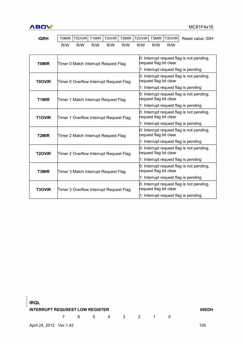
MC81F4x16
April 24, 2012 Ver.1.42 105
IQRH T0MIR T0OVIR T1MIR TIOVIR T2MIR T2OVIR T3MIR T3OVIR Reset value: 00H R/W R/W R/W R/W R/W R/W R/W R/W
0: Interrupt request flag is not pending, request flag bit clear T0MIR Timer 0 Match Interrupt Request Flag 1: Interrupt request flag is pending 0: Interrupt request flag is not pending, request flag bit clear T0OVIR Timer 0 Overflow Interrupt Request Flag 1: Interrupt request flag is pending 0: Interrupt request flag is not pending, request flag bit clear T1MIR Timer 1 Match Interrupt Request Flag 1: Interrupt request flag is pending 0: Interrupt request flag is not pending, request flag bit clear T1OVIR Timer 1 Overflow Interrupt Request Flag 1: Interrupt request flag is pending 0: Interrupt request flag is not pending, request flag bit clear T2MIR Timer 2 Match Interrupt Request Flag 1: Interrupt request flag is pending 0: Interrupt request flag is not pending, request flag bit clear T2OVIR Timer 2 Overflow Interrupt Request Flag 1: Interrupt request flag is pending 0: Interrupt request flag is not pending, request flag bit clear T3MIR Timer 3 Match Interrupt Request Flag 1: Interrupt request flag is pending 0: Interrupt request flag is not pending, request flag bit clear T3OVIR Timer 3 Overflow Interrupt Request Flag 1: Interrupt request flag is pending
IRQL INTERRUPT REQUSEST LOW REGISTER 00EDH
7 6 5 4 3 2 1 0

MC81F4x16
106 April 24, 2012 Ver.1.42
IRQL IICIR SIOIR WTIR URIR UTIR WDTIR – BITIR Reset value: 00H R/W R/W R/W R/W R/W R/W – R/W
0: Interrupt request flag is not pending, request flag bit clear IICIR IIC Interrupt Request Flag 1: Interrupt request flag is pending 0: Interrupt request flag is not pending, request flag bit clear SIOIR SIO Interrupt Request Flag 1: Interrupt request flag is pending 0: Interrupt request flag is not pending, request flag bit clear WTIR Watch Timer Interrupt Request Flag 1: Interrupt request flag is pending 0: Interrupt request flag is not pending, request flag bit clear URIR UART Rx Interrupt Request Flag 1: Interrupt request flag is pending 0: Interrupt request flag is not pending, request flag bit clear UTIR UART Tx Interrupt Request Flag 1: Interrupt request flag is pending 0: Interrupt request flag is not pending, request flag bit clear WDTIR Watchdog Timer Interrupt Request Flag 1: Interrupt request flag is pending
– bit1 Not used for MC81F4x16 0: Interrupt request flag is not pending, request flag bit clear BTIR Basic Timer Interrupt Request Flag 1: Interrupt request flag is pending
INTFH INTERRUPT FLAG HIGH REGISTER 00EEH
7 6 5 4 3 2 1 0

MC81F4x16
April 24, 2012 Ver.1.42 107
INTFH T0MIF T0OVIF T1MIF TIOVIF T2MIF T2OVIF T3MIF T3OVIF Reset value: 00H R/W R/W R/W R/W R/W R/W R/W R/W
0: No generation
T0MIF Timer 0 Match Interrupt Flag Bit 1: Generation 0: No generation
T0OVIF Timer 0 Overflow Interrupt Flag Bit 1: Generation 0: No generation
T1MIF Timer 1 Match Interrupt Flag Bit 1: Generation 0: No generation
T1OVIF Timer 1 Overflow Interrupt Flag Bit 1: Generation 0: No generation
T2MIF Timer 2 Match Interrupt Flag Bit 1: Generation 0: No generation
T2OVIF Timer 2 Overflow Interrupt Flag Bit 1: Generation 0: No generation
T3MIF Timer 3 Match Interrupt Flag Bit 1: Generation 0: No generation
T3OVIF Timer 3 Overflow Interrupt Flag Bit 1: Generation
INTFL INTERRUPT FLAG LOW REGISTER 00EFH
7 6 5 4 3 2 1 0 INTFL IICIF – – – – – URIF UTIF Reset value: 00H
R/W – – – – – R/W R/W
0: No generation IICIF IIC Interrupt Flag Bit
1: Generation – bit6 – bit2 Not used for MC81F4x16
0: No generation URIF UART Rx Interrupt Flag Bit
1: Generation 0: No generation
UTIF UART Tx Interrupt Flag Bit 1: Generation
Note: When you use ‘Shard Interrupt Vector’, those INTFH and INTFL are used to recognize which interrupt is generated. See ‘11.4 Shared Interrupt Vector’ on page 110 for more information.
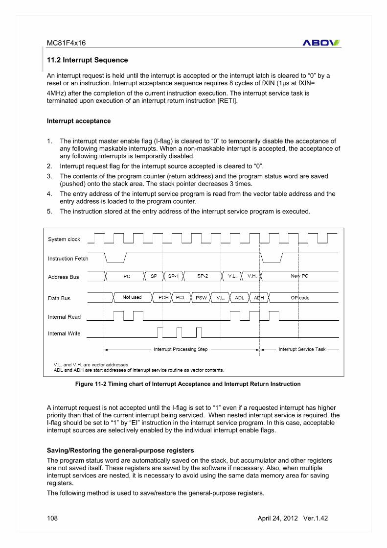
MC81F4x16
108 April 24, 2012 Ver.1.42
11.2 Interrupt Sequence
An interrupt request is held until the interrupt is accepted or the interrupt latch is cleared to “0” by a reset or an instruction. Interrupt acceptance sequence requires 8 cycles of fXIN (1μs at fXIN= 4MHz) after the completion of the current instruction execution. The interrupt service task is terminated upon execution of an interrupt return instruction [RETI]. Interrupt acceptance 1. The interrupt master enable flag (I-flag) is cleared to “0” to temporarily disable the acceptance of
any following maskable interrupts. When a non-maskable interrupt is accepted, the acceptance of any following interrupts is temporarily disabled.
2. Interrupt request flag for the interrupt source accepted is cleared to “0”. 3. The contents of the program counter (return address) and the program status word are saved
(pushed) onto the stack area. The stack pointer decreases 3 times. 4. The entry address of the interrupt service program is read from the vector table address and the
entry address is loaded to the program counter. 5. The instruction stored at the entry address of the interrupt service program is executed.
A interrupt request is not accepted until the I-flag is set to “1” even if a requested interrupt has higher priority than that of the current interrupt being serviced. When nested interrupt service is required, the I-flag should be set to “1” by “EI” instruction in the interrupt service program. In this case, acceptable interrupt sources are selectively enabled by the individual interrupt enable flags. Saving/Restoring the general-purpose registers The program status word are automatically saved on the stack, but accumulator and other registers are not saved itself. These registers are saved by the software if necessary. Also, when multiple interrupt services are nested, it is necessary to avoid using the same data memory area for saving registers. The following method is used to save/restore the general-purpose registers.
Figure 11-2 Timing chart of Interrupt Acceptance and Interrupt Return Instruction

MC81F4x16
April 24, 2012 Ver.1.42 109
Example: Register save using push and pop instructions.
INTxx :
PUSH A
PUSH X
PUSH Y
;SAVE XCC.
;SAVE X REG.
;SAVE Y REG.
;; interrupt processing ;;
POP Y
POP X
POP A
RETI
;RESTORE Y REG.
;RESTORE X REG.
;RESTORE ACC.
;RETURN
General-purpose register save/restore using push and pop instructions;
Figure 11-3 Saving/Restoring in Interrupt Routine

MC81F4x16
110 April 24, 2012 Ver.1.42
11.3 BRK Interrupt
Software interrupt can be invoked by BRK instruction, which has the lowest priority order. Interrupt vector address of BRK is shared with the vector of TCALL 0 (Refer to Program Memory Section). When BRK interrupt is generated, B-flag of PSW is set to distinguish BRK from TCALL 0. Each processing step is determined by B-flag as shown in Figure
11.4 Shared Interrupt Vector
Some interrupts share the interrupt vector address. To recognize which interrupt is occurred, some interrupt flag registers are used. Note that, interrupt request bits are cleared after call the interrupt service routine. So interrupt request bits can not be used to recognize which interrupt is occurred. UART In case of using interrupts of UART Tx and UART Rx together, it is necessary to check UTIF and URIF in the interrupt service routine to find out which interrupt is occurred. Because the UART Tx and UART Rx share the one interrupt vector address. These flag bits must be cleared by software after reading this register. ( UTIF and URIF are placed in INTFL register ) External Interrupt Group In case of using interrupts of Ext group. It is necessary to check the EINTF register in the interrupt service routine to find out which external interrupt is occurred. Because the 8 external interrupts share the one interrupt vector address. These flag bits must be cleared by software after reading this register. Timer match / overflow In case of using interrupts of Timer match and overflow together, it is necessary to check the INTFH register in the interrupt service routine to find out which interrupt is occurred. Because the timer match and overflow share the on interrupt vector address. See ‘INTFH’ on page 106 to know which bit is which.
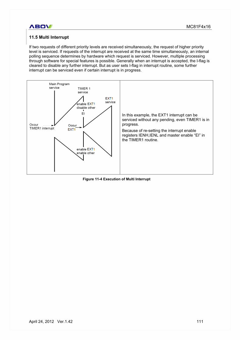
MC81F4x16
April 24, 2012 Ver.1.42 111
11.5 Multi Interrupt
If two requests of different priority levels are received simultaneously, the request of higher priority level is serviced. If requests of the interrupt are received at the same time simultaneously, an internal polling sequence determines by hardware which request is serviced. However, multiple processing through software for special features is possible. Generally when an interrupt is accepted, the I-flag is cleared to disable any further interrupt. But as user sets I-flag in interrupt routine, some further interrupt can be serviced even if certain interrupt is in progress.
In this example, the EXT1 interrupt can be serviced without any pending, even TIMER1 is in progress. Because of re-setting the interrupt enable registers IENH,IENL and master enable “EI” in the TIMER1 routine.
Figure 11-4 Execution of Multi Interrupt

MC81F4x16
112 April 24, 2012 Ver.1.42
11.6 Interrupt Vector & Priority Table
Address Interrupt INT number Priority
0FFE0H Basic Interval Timer INT0 15 ( lowest priority)
0FFE2H Watchdog Timer INT1 14
0FFE4H Timer 3 match/overflow INT2 13
0FFE6H Timer 2 match/overflow INT3 12
0FFE8H Timer 1 match/overflow INT4 11
0FFEAH Timer 0 match/overflow INT5 10
0FFECH UART Rx/Tx INT6 9
0FFEEH Watch Timer INT7 8
0FFF0H SIO INT8 7
0FFF2H IIC INT9 6
0FFF4H External Group INT10 5
0FFF6H External 6 INT11 4
0FFF8H External 5 INT12 3
0FFFAH External 3 INT13 2
0FFFCH External 1 INT14 1
0FFFEH RESET INT15 0 ( highest priority)
Note : External Interrupt Group = (EXT0, EXT2, EXT4, EXT7 – EXT11)
Table 11-1 Interrupt Vector & Priority

MC81F4x16
April 24, 2012 Ver.1.42 113
12. EXTERNAL INTERRUPTS The external interrupt pins are edge triggered depending on the ‘external interrupt registers’. The edge detection of external interrupt has three transition activated mode: rising edge, falling edge, and both edge.
12.1 Registers
EINT0H – EXT 2~5 / R04~R07 R0 PORT EXTERNAL INTERRUPT ENABLE HIGH REGISTER 00CAH A reset clears the EINT0H register to ‘00H’, disables EXT5-EXT2 interrupt. You can use EINT0H register setting to select Disable interrupt or Enable interrupt (by falling, rising, or both falling and rising edge).
7 6 5 4 3 2 1 0 EINT0H EXT5IE EXT4IE EXT3IE EXT2IE Reset value: 00H
R/W R/W R/W R/W R/W R/W R/W R/W
EXT5IE R07/EXT5 External Interrupt Enable Bits
EXT4IE R06/EXT4 External Interrupt Enable Bits
EXT3IE R05/EXT3 External Interrupt Enable Bits
EXT2IE R04/EXT2 External Interrupt Enable Bits
00: Disable Interrupt 01: Enable Interrupt by falling edge 10: Enable Interrupt by rising edge 11: Enable Interrupt by both falling and rising edge
EINT0L – EXT 10,11,0,1 / R00~R03 R0 PORT EXTERNAL INTERRUPT ENABLE LOW REGISTER 00CBH A reset clears the EINT0L register to ‘00H’, disables EXT1-EXT0, EXT11-EXT10 interrupt. You can use EINT0L register setting to select Disable interrupt or Enable interrupt (by falling, rising, or both falling and rising edge).
7 6 5 4 3 2 1 0 EINT0L EXT1IE EXT0IE EXT11IE EXT10IE Reset value: 00H
R/W R/W R/W R/W R/W R/W R/W R/W
EXT1IE R03/EXT1 External Interrupt Enable Bits
EXT0IE R02/EXT0 External Interrupt Enable Bits
EXT11IE R01/EXT11 External Interrupt Enable Bits
EXT10IE R00/EXT10 External Interrupt Enable Bits
00: Disable Interrupt 01: Enable Interrupt by falling edge 10: Enable Interrupt by rising edge 11: Enable Interrupt by both falling and rising edge

MC81F4x16
114 April 24, 2012 Ver.1.42
EINT1 – EXT 6~9 / R10~R13 R1 PORT EXTERNAL INTERRUPT ENABLE REGISTER 00D7H A reset clears the EINT1 register to ‘00H’, disables EXT9-EXT6 interrupts. You can use EINT1 register setting to select Disable interrupt or Enable interrupt (by falling, rising, or both falling and rising edge).
7 6 5 4 3 2 1 0 EINT1 EXT9IE EXT8IE EXT7IE EXT6IE Reset value: 00H
R/W R/W R/W R/W R/W R/W R/W R/W
EXT9IE R13/EXT9 External Interrupt Enable Bits
EXT8IE R12/EXT8 External Interrupt Enable Bits
EXT7IE R11/EXT7 External Interrupt Enable Bits
EXT6IE R10/EXT6 External Interrupt Enable Bits
00: Disable Interrupt 01: Enable Interrupt by falling edge 10: Enable Interrupt by rising edge 11: Enable Interrupt by both falling and rising edge

MC81F4x16
April 24, 2012 Ver.1.42 115
ERQ0 – EXT 10,11,0~5 / R00~R07 R0 PORT EXTERNAL INTERRUPT REQUEST REGISTER 00CCH When an interrupt is generated, the bit of ERQ0 that generated it is cleared by the hardware when the service routine is vectored to only if the interrupt was transition-activated.
7 6 5 4 3 2 1 0 ERQ0 EXT5IR EXT4IR EXT3IR EXT2IR EXT1IR EXT0IR EXT11IR EXT10IR Reset value: 00H
R/W R/W R/W R/W R/W R/W R/W R/W
EXT5IR R07/EXT5 External Interrupt Request Flag
EXT4IR R06/EXT4 External Interrupt Request Flag
EXT3IR R05/EXT3 External Interrupt Request Flag
EXT2IR R04/EXT2 External Interrupt Request Flag
EXT1IR R03/EXT1 External Interrupt Request Flag EXT0IR R02/EXT0 External Interrupt Request Flag EXT11IR R01/EXT11 External Interrupt Request Flag
EXT10IR R00/EXT10 External Interrupt Request Flag
0: Interrupt request flag is not pending, request flag bit clear 1: Interrupt request flag is pending
ERQ1 – EXT 6~9 / R10~R13 R1 PORT EXTERNAL INTERRUPT REQUEST REGISTER 00D8H When an interrupt is generated, the bit of ERQ1 that generated it is cleared by the hardware when the service routine is vectored to only if the interrupt was transition-activated.
7 6 5 4 3 2 1 0 ERQ1 – – – – EXT9IR EXT8IR EXT7IR EXT6IR Reset value: 00H
– – – – R/W R/W R/W R/W
– bit7 – bit4 Not used for MC81F4x16 EXT9IR R03/EXT9 External Interrupt Request Flag EXT8IR R02/EXT8 External Interrupt Request Flag EXT7IR R01/EXT7 External Interrupt Request Flag EXT6IR R00/EXT6 External Interrupt Request Flag
0: Interrupt request flag is not pending, request flag bit clear 1: Interrupt request flag is pending

MC81F4x16
116 April 24, 2012 Ver.1.42
EINTF EXTERNAL INTERRUPT FLAG REGISTER 00CDH
7 6 5 4 3 2 1 0 EINTFH INT0IF INT2IF INT4IF INT7IF INT8IF INT9IF INT10IF INT11IF Reset value: 00H
R/W R/W R/W R/W R/W R/W R/W R/W
EXT0IF EXT0 External Interrupt Flag
EXT2IF EXT2 External Interrupt Flag
EXT4IF EXT4 External Interrupt Flag
EXT7IF EXT7 External Interrupt Flag
EXT8IF EXT8 External Interrupt Flag
EXT9IF EXT9 External Interrupt Flag
EXT10IF EXT10 External Interrupt Flag
EXT11IF EXT11 External Interrupt Flag
0: Not generated 1: Generated
12.2 Procedure
To generate external interrupt, following steps are required, 1. Prepare external interrupt sub-routine. 2. Set external interrupt pins to read mode 3. Enable the external interrupt and select the edge mode. 4. Make sure global interrupt is enabled(use ‘EI’ instruction).
After finish above steps, the external interrupt sub-routine is calling, when the edge is detected. When the generated external interrupt is one of the external interrupts group, the EINTF register is used to recognize which external interrupt is generated.

MC81F4x16
April 24, 2012 Ver.1.42 117
13. CLOCK GENERATOR
As shown in Figure 13-1, the clock generator produces the basic clock pulses for the CPU and the peripheral hardware. It contains two oscillators which are main-system oscillator and a sub-oscillator. And for the system and the peripheral clocks, one oscillator is selected by the SCLK bit of the OSCSEL register. There are few clock sources for main-oscillator which are listed below.
- Crystal / Ceramic Oscillator / (External Clock). - 8, 4, 2, 1 MHz Internal RC Oscillator. - External RC Oscillator.
Note that, one of the clock sources is used for main-oscillator based on the ROM option (See ‘8 . ROM OPTION’ at page 61). Only one clock source is available for sub-oscillator which is ‘Crystal / Ceramic Oscillator / (External Clock )’. To the peripheral block, the clock among the not-divided original clocks and divided by 2, 4..., up to 4096 can be provided. Peripheral clock is enabled or disabled by STOP instruction. When the system is fall in stop mode, only selected oscillator(by SCLK bit) is stopped. Unselected oscillator is not affected by stop mode.
Figure 13-1 Block Diagram of Clock Generator

MC81F4x16
118 April 24, 2012 Ver.1.42
13.1 Registers
OSCSEL OSCILLATOR SELECT REGISTER 00BCH
7 6 5 4 3 2 1 0 OSCSEL – – – – – MOSC SOSC SCLK Reset value: 00H
– – – – – R/W R/W R/W
– bit7 – bit3 Not used for MC81F4x16 0: Main oscillator RUN
MOSC Main Oscillator Control Bit 1: Main oscillator STOP 0: Sub oscillator RUN
SOSC Sub Oscillator Control Bit 1: Sub oscillator STOP 0: Select main oscillator for system clock
SCLK System Clock Selection Bit 1: Select sub oscillator for system clock

MC81F4x16
April 24, 2012 Ver.1.42 119
14. OSCILLATION CIRCUITS There are few example circuits for main and sub oscillators. Oscillation circuit is designed to be used either with a ceramic resonator or crystal oscillator. Since each crystal and ceramic resonator have their own characteristics, the user should consult the crystal manufacturer for appropriate values of external components.
14.1 Main Oscillation Circuits
C1 C2
XIN XOUT
C1, C2 = 10 ~ 30 pF * The example load capacitor value(C1, C2) is common value but may not be appropriate for some crystal or ceramic resonator.
XIN XOUT
Xout pin can be used as a normal pin.
Figure 14-1 Crystal/Ceramic Oscillator
Figure 14-2 External Clock
Figure 14-3 External RC Oscillator

MC81F4x16
120 April 24, 2012 Ver.1.42
Xout and Xin pins can be used as normal pins
14.2 Sub Oscillation Circuits
C1 C2
XIN XOUT
C1, C2 = 10 ~ 30 pF * The example load capacitor value(C1, C2) is common value but may not be appropriate for some crystal or ceramic resonator.
XIN XOUT
Figure 14-4 Internal RC Oscillator
Figure 14-5 Crystal/Ceramic Oscillator
Figure 14-6 External Clock

MC81F4x16
April 24, 2012 Ver.1.42 121
14.3 PCB Layout
For reference, here is a example layout for oscillator circuit.
Note : Minimize the wiring length. Do not allow the wiring to intersect with other signal conductors. Do not allow the wiring to come near changing high current. Set the potential of the grounding position of the oscillator capacitor to that of VSS. Do not ground it to any ground pattern where high current is present. Do not fetch signals from the oscillator.
Figure 14-7 Layout of Oscillator PCB circuit
MC81F4x16
122 April 24, 2012 Ver.1.42
15. BASIC INTERVAL TIMER The MC81F4x16 has one 8-bit Basic Interval Timer that is free-run and can not be stopped except when peripheral clock is stopped. The Basic Interval Timer generates the time base for watchdog timer counting. It also provides a Basic interval timer interrupt. The 8-bit Basic interval timer register (BTCR) is increased every internal count pulse which is divided by prescaler. Since prescaler has divided ratio by 8 to 1024, the count rate is 1/8 to 1/1024 of the oscillator frequency. As the count overflow from FFH to 00H, this overflow causes the interrupt to be generated. The Basic Interval Timer is controlled by the clock control register (CKCTLR). When write "1" to bit BTCL of CKCTLR, BTCR register is cleared to "0" and restart to count-up. The bit BTCL becomes "0" after one machine cycle by hardware. The bit WDTON decides Watchdog Timer or the normal 7-bit timer. Source clock can be selected by lower 3 bits of CKCTLR.

MC81F4x16
April 24, 2012 Ver.1.42 123
15.1 Registers
CKCTLR CLOCK CONTROL REGISTER 00F2H
7 6 5 4 3 2 1 0 CKCTLR – – – WDTON BTCL BTS Reset value: 17H
– – – R/W R/W R/W R/W R/W
– bit7 – bit5 Not used for MC81F4x16 0: Operate as 7-bit timer
WDTON Watchdog Timer Enable Bit 1: Enable Watchdog timer 0: Normal operation (free-run)
BTCL Basic Timer Clear Bit 1: Clear 8-bit counter (BITR) to “0”, This bit becomes 0 automatically after onemachine cycle, and starts counting. 000: fxin/8 001: fxin/16 010: fxin/32 011: fxin/64 100: fxin/128 101: fxin/256 110: fxin/512
BTS Basic Interval Timer Source Clock Selection Bits
111: fxin/1024
CKCTLR[2:0] Source clock Interrupt(overflow) period (ms) @ fxin = 8MHz
000 fxin/8 0.256 001 fxin/16 0.512 010 fxin/32 1.024 011 fxin/64 2.048 100 fxin/128 4.096 101 fxin/256 8.192 110 fxin/512 16.384 111 fxin/1024 32.768
BTCR BASIC TIMER COUNTER REGISTER 00F1H
7 6 5 4 3 2 1 0 BTCR One byte register Reset value: XXH
R R R R R R R R
Figure 15-1 Basic Interval Timer Interrupt Period

MC81F4x16
124 April 24, 2012 Ver.1.42
A 8 bit count register for the basic interval timer.

MC81F4x16
April 24, 2012 Ver.1.42 125
16. WATCH DOG TIMER
The watchdog timer rapidly detects the CPU malfunction such as endless looping caused by noise or the like, and resumes the CPU to the normal state. The watchdog timer signal for detecting malfunction can be selected either a reset CPU or a interrupt request. When the watchdog timer is not being used for malfunction detection, it can be used as a timer to generate an interrupt at fixed intervals. The watchdog timer uses the Basic Interval Timer as a clock source. The watchdog timer consists of 7-bit binary counter and the watchdog timer data register. When the value of 7-bit binary counter is equal to the lower 7 bits of WDTR, the interrupt request flag is generated. This can be used as Watchdog timer interrupt or reset the CPU in accordance with the bit WDTON. Watchdog reset feature is disabled when the watchdog timer status register(WDTSR) value is ‘0A5h’. Note that, WDTSR’s reset value is ‘00h’. And reset value of WDTON is ‘1’. So watchdog timer reset is enabled at reset time.
Figure 16-1 Block diagram of Basic Interval Timer/Watchdog Timer

MC81F4x16
126 April 24, 2012 Ver.1.42
16.1 Registers
WDTR WATCHDOG TIMER REGISTER 00F4H
7 6 5 4 3 2 1 0 WDTR WDTCL WDTCMP Reset value: 7FH
R/W R/W R/W R/W R/W R/W R/W R/W
0: Free-run count
WDTCL Watchdog Timer Clear Bit 1: When the WDTCL is set to “1”, binary
counter is cleared to “0”. And the WDTCL becomes “0” automatically after one machine cycle. Counter count up again.
WDTCMP bit6 – bit0 7-bit compare data
WDTSR WATCHDOG TIMER STATUS REGISTER 00F6H
7 6 5 4 3 2 1 0 WDTSR One byte register Reset value: 00H
R/W R/W R/W R/W R/W R/W R/W R/W
10100101: Disable watchdog timer function Watchdog Timer Function Disable Code (for System Reset) Others: Enable watchdog timer function
Figure 16-2 Watchdog Timer Timing

MC81F4x16
April 24, 2012 Ver.1.42 127
17. WATCH TIMER Watch timer functions include real-time and watch-time measurement and interval timing for the system clock. Watch timer has the following functional components: - Real time and watch time measurement - Using a main or sub clock source (main clock divided by 27(fx/128) or sub clock(fxt)) - Timing tests in high-speed mode - Watch timer interrupt generation - Watch timer status and control register (WTSCR)
Figure 17-1 Watch Timer Block Diagram

MC81F4x16
128 April 24, 2012 Ver.1.42
17.1 Registers
WTSCR WATCH TIMER STATUS AND CONTROL REGISTER 00F0H
7 6 5 4 3 2 1 0 WTSCR – WTEN WTSS – – WTCS Reset value: 00H
– R/W R/W R/W R/W – – R/W A reset clears WTSCR register to ‘00H’. This disables the watch timer. So, if you want to use the watch timer, you must write appropriate value to WTSCR register. When the watch timer interrupt sub-routine is serviced, the watch timer interrupt request flag bit, WTIR is automatically cleared.
– bit7 Not used for MC81F4x16
0:Disable watch timer; Clear frequency Dividing circuits WTEN Watch Timer Enable Bit 1: Enable watch timer 000: Set watch timer interrupt to 60.0s 001: Set watch timer interrupt to 30.0s 010: Not available 011: Not available 100: Set watch timer interrupt to 1.0s 101: Set watch timer interrupt to 0.5s 110: Set watch timer interrupt to 0.25s
WTSS Watch Timer Speed Selection Bits
111: 1/100s stop watch for real timer – bit2 – bit1 Not used for MC81F4x16
0: Select main clock divided by 27 (fx/128) WTCS Watch Timer Clock Selection Bit
1: Select sub clock (fxt)
Note: Main system clock frequency (fx) is assumed to be 4.19 MHz.
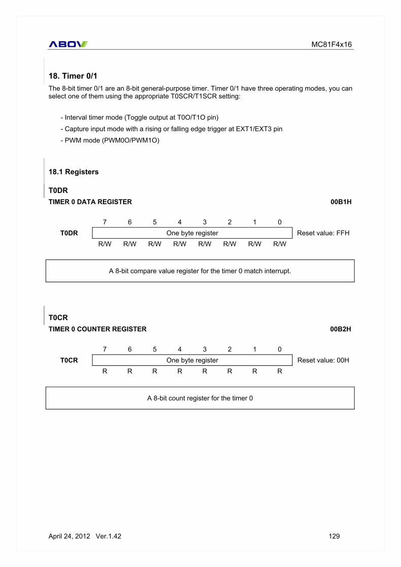
MC81F4x16
April 24, 2012 Ver.1.42 129
18. Timer 0/1 The 8-bit timer 0/1 are an 8-bit general-purpose timer. Timer 0/1 have three operating modes, you can select one of them using the appropriate T0SCR/T1SCR setting: - Interval timer mode (Toggle output at T0O/T1O pin)
- Capture input mode with a rising or falling edge trigger at EXT1/EXT3 pin
- PWM mode (PWM0O/PWM1O)
18.1 Registers
T0DR TIMER 0 DATA REGISTER 00B1H
7 6 5 4 3 2 1 0 T0DR One byte register Reset value: FFH
R/W R/W R/W R/W R/W R/W R/W R/W
A 8-bit compare value register for the timer 0 match interrupt.
T0CR TIMER 0 COUNTER REGISTER 00B2H
7 6 5 4 3 2 1 0 T0CR One byte register Reset value: 00H
R R R R R R R R
A 8-bit count register for the timer 0
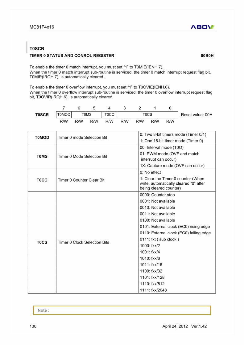
MC81F4x16
130 April 24, 2012 Ver.1.42
T0SCR TIMER 0 STATUS AND CONROL REGISTER 00B0H To enable the timer 0 match interrupt, you must set “1” to T0MIE(IENH.7). When the timer 0 match interrupt sub-routine is serviced, the timer 0 match interrupt request flag bit, T0MIR(IRQH.7), is automatically cleared. To enable the timer 0 overflow interrupt, you must set “1” to T0OVIE(IENH.6). When the timer 0 overflow interrupt sub-routine is serviced, the timer 0 overflow interrupt request flag bit, T0OVIR(IRQH.6), is automatically cleared.
7 6 5 4 3 2 1 0 T0SCR T0MOD T0MS T0CC T0CS Reset value: 00H
R/W R/W R/W R/W R/W R/W R/W R/W
0: Two 8-bit timers mode (Timer 0/1) T0MOD Timer 0 mode Selection Bit
1: One 16-bit timer mode (Timer 0) 00: Interval mode (T0O) 01: PWM mode (OVF and match interrupt can occur)
T0MS Timer 0 Mode Selection Bit
1X: Capture mode (OVF can occur) 0: No effect
T0CC Timer 0 Counter Clear Bit 1: Clear the Timer 0 counter (When write, automatically cleared “0” after being cleared counter) 0000: Counter stop 0001: Not available 0010: Not available 0011: Not available 0100: Not available 0101: External clock (EC0) rising edge 0110: External clock (EC0) falling edge 0111: fxt ( sub clock ) 1000: fxx/2 1001: fxx/4 1010: fxx/8 1011: fxx/16 1100: fxx/32 1101: fxx/128 1110: fxx/512
T0CS Timer 0 Clock Selection Bits
1111: fxx/2048
Note :

MC81F4x16
April 24, 2012 Ver.1.42 131
You must set the T0CC(T0SCR.4) bit after set T0DR register. The timer 0 counter value is compared with timer 0 buffer register instead of T0DR. And T0DR value is copied to timer 0 buffer register when 1)T0CC is set 2)T0OVIR is set 3) T0MIR is set.
T1DR TIMER 1 DATA REGISTER 00B4H
7 6 5 4 3 2 1 0 T1DR One byte register Reset value: FFH
R/W R/W R/W R/W R/W R/W R/W R/W
A 8-bit compare value register for the timer 1 match interrupt.
T1CR TIMER 0 COUNTER REGISTER 00B5H
7 6 5 4 3 2 1 0 T1CR One byte register Reset value: 00H
R R R R R R R R
A 8-bit count register for the timer 1

MC81F4x16
132 April 24, 2012 Ver.1.42
T1SCR TIMER 1 STATUS AND CONTROL REGISTER 00B3H To enable the timer 1 match interrupt, you must set “1” to T1MIE. When the timer 1 match interrupt sub-routine is serviced, the timer 1 match interrupt request flag bit, T1MIR(IRQH.5), is automatically cleared.. To enable the timer 1 overflow interrupt, you must set “1” to T1OVIE. When the timer 1 overflow interrupt sub-routine is serviced, the timer 1 overflow interrupt request flag bit, T1OVIR(IRQH.4), is automatically cleared.
7 6 5 4 3 2 1 0 T1SCR – T1MS T1CC T1CS Reset value: 00H
R/W R/W R/W R/W R/W R/W R/W R/W
– bit7 Not used for MC81F4x16 00: Interval mode (T1O) 01: PWM mode (OVF and match interrupt can occur)
T1MS Timer 1 Mode Selection Bit
1X: Capture mode (OVF can occur) 0: No effect
T1CC Timer 1 Counter Clear Bit 1: Clear the Timer 1 counter (When write, automatically cleared “0” after being cleared counter) 0000: Counter stop 0001: Not available 0010: Not available 0011: Not available 0100: Not available 0101: External clock (EC1) rising edge 0110: External clock (EC1) falling edge 0111: fxt ( sub clock ) 1000: fxx/1 1001: fxx/2 1010: fxx/4 1011: fxx/8 1100: fxx/16 1101: fxx/64 1110: fxx/256
T1CS Timer 1 Clock Selection Bits
1111: fxx/1024
Note : You must set the T1CC(T1SCR.4) bit after set T1DR register. The timer 1 counter value is compared with timer 1 buffer register instead of T1DR. And T1DR value is copied to timer 1 buffer.

MC81F4x16
April 24, 2012 Ver.1.42 133
18.2 Timer 0 8-Bit Mode
Timer 0 has the following functional components:
- Clock frequency divider (fxx divided by 2048, 512, 128, 32, 16, 8, 4, 2, fxt) with multiplexer
- External clock input pin, EC0 (R02)
- I/O pins for capture input, EXT1 (R03) or PWM or match output PWM0O/T0O (R03)
- 8-bit counter (T0CR), 8-bit comparator, and 8-bit reference data register (T0DR)
- Timer 0 status and control register (T0SCR)
- Timer 0 overflow interrupt and match interrupt generation
Figure 18-1 8-bit Timer 0 Block Diagram

MC81F4x16
134 April 24, 2012 Ver.1.42
Function Description Interval Timer Mode A match signal is generated and T0O pins are toggled when the T0CR register value equals the T0DR register value. The match signal generates a timer match interrupt and clears the T0CR register. Pulse Width Modulation Mode Pulse width modulation (PWM) mode lets you program the width (duration) of the pulse that is output at the PWM0O pin. As in interval timer mode, a match signal is generated when the counter value is identical to the value written to the T0DR register. In PWM mode, however, the match signal does not clear the counter. Instead, it runs continuously, overflowing at FFH, and then continues incrementing from 00H. Although you can use the match signal to generate a timer 0 overflow interrupt, interrupts are not typically used in PWM-type applications. Instead, the pulse at the PWM0O pin is held to Low level as long as the reference data value is less than or equal to ( ≤ ) the counter value and then the pulse is held to High level for as long as the data value is greater than ( > ) the counter value. One pulse width is equal to tCLK * 256. So, the period and duty times are, Duty = tCLK * (T0DR + 1) Period = tCLK * 256 In order to generate the PWM0O signal, 3 steps are required,
Steps Example C code
Make sure the PWM0O port is set by PWM output mode T0CONM = 0x03;
Set the T0DR value properly T0DR = 25;
Set the T0SCR register properly T0SCR = 0x38;
Capture Mode In capture mode, you have to set EXT1 interrupt. When the EXT1 interrupt is occurred, the T0CR register value is loaded into the T0DR register and the T0CR register is cleared. And the timer 0 overflow interrupt is generated whenever the T0CR value is overflowed. So, If you count how many overflow is occurred and read the T0DR value in EXT1 interrupt routine, it is possible to measure the time between two EXT1 interrupts. Or it is possible to measure the time from the T0 initial time to the EXT1 interrupt occurred time. The time = ( 256 * tCLK ) * overflow_count + (tCLK * T0DR)
Note ‘tCLK’ is the period time of the timer-counter’s clock source You must set the T0DR value before set the T0SCR register. Because T0DR value is fetched when the count is started(the T0CC bit is set) or match/overflow event is occurred.

MC81F4x16
April 24, 2012 Ver.1.42 135
18.3 Timer 1 8-Bit Mode
T1CS
T1MIR
MUX
EINT0L
EXT3Timer 1 Buffer Register
Timer 1 Data Register
8-Bit Up Counter(Read - only) R
8
Data BUS
8
T1OVIR
T1OVIE
OVF
Match
M
U
X
EC1
fxx/4fxx/2fxx/1
fxt
Counter stop8-Bit Comparator
T1MIE
Data BUS
Clear
fxx/256fxx/64fxx/16fxx/8
Clear
EXT3Interrupt
fxx/1024 Timer 1 overflow INT enable
Timer 1 Overflow INT request
Timer 1 INT enable
Timer 1 Match INT request
T1CR
T1DR
T1O/PWM1O
T1CC
Match signalOverflow signal
MUX
T1MS
T1CCMatch signal
T1 Overflow Interrupt
T1OVIF
T1 MatchInterrupt
T1MIF
Timer 1 has the following functional components:
- Clock frequency divider (fxx divided by 1024, 256, 64, 16, 8, 4, 2, 1, fxt) with multiplexer
- External clock input pin, EC1 (R04)
- I/O pins for capture input, EXT3 (R05) or PWM or match output PWM1O/T1O (R05)
- 8-bit counter (T1CR), 8-bit comparator, and 8-bit reference data register (T1DR)
- Timer 1 status and control register (T1SCR)
- Timer 1 overflow interrupt and match interrupt generation
Figure 18-2 8-bit Timer 1 Block Diagram

MC81F4x16
136 April 24, 2012 Ver.1.42
Function Description Interval Timer Mode A match signal is generated and T1O pins are toggled when the T1CR register value equals the T1DR register value. The match signal generates a timer match interrupt and clears the T1CR register. Pulse Width Modulation Mode Pulse width modulation (PWM) mode lets you program the width (duration) of the pulse that is output at the PWM1O pin. As in interval timer mode, a match signal is generated when the counter value is identical to the value written to the T1DR register. In PWM mode, however, the match signal does not clear the counter. Instead, it runs continuously, overflowing at FFH, and then continues incrementing from 00H. Although you can use the match signal to generate a timer 1 overflow interrupt, interrupts are not typically used in PWM-type applications. Instead, the pulse at the PWM1O pin is held to Low level as long as the reference data value is less than or equal to ( ≤ ) the counter value and then the pulse is held to High level for as long as the data value is greater than ( > ) the counter value. One pulse width is equal to tCLK * 256. So, the period and duty times are, Duty = tCLK * (T1DR + 1) Period = tCLK * 256 In order to generate the PWM1O signal, 3 steps are required,
Steps Example C code
Make sure the PWM1O port is set by PWM output mode T1CONM = 0xC0;
Set the T1DR value properly T1DR = 25;
Set the T1SCR register properly T1SCR = 0x38;
Capture Mode In capture mode, you have to set EXT3 interrupt. When the EXT3 interrupt is occurred, the T1CR register value is loaded into the T1DR register and the T1CR register is cleared. And the timer 1 overflow interrupt is generated whenever the T1CR value is overflowed. So, If you count how many overflow is occurred and read the T1DR value in EXT3 interrupt routine, it is possible to measure the time between two EXT3 interrupts. Or it is possible to measure the time from the T1 initial time to the EXT3 interrupt occurred time. The time = ( 256 * tCLK ) * overflow_count + (tCLK * T1DR)
Note ‘tCLK’ is the period time of the timer-counter’s clock source You must set the T1DR value before set the T1SCR register. Because T1DR value is fetched when the count is started(the T1CC bit is set) or match/overflow event is occurred.

MC81F4x16
April 24, 2012 Ver.1.42 137
18.4 Timer 0 16-BIT Mode
The 16-bit timer 0 is a 16-bit general-purpose timer. Timer 0 has three operating modes, you can select one of them using the appropriate T0SCR setting:
- Interval timer mode (Toggle output at T0O pin)
- Capture input mode with a rising or falling edge trigger at EXT1 pin
- PWM mode (PWM0O) The 16-bit timer 0 has the following functional components:
- Clock frequency divider (fxx divided by 2048, 512, 128, 32, 16, 8, 4, 2, fxt) with multiplexer
- External clock input pin, EC0 (R02)
- I/O pins for capture input, EXT1 (R03) or PWM or match output PWM0O/T0O (R03)
- 16-bit counter (T0CR+T1CR), 16-bit comparator, and 16-bit reference data register (T0DR+T1DR)
- Timer 0 status and control register (T0SCR)
- Timer 0 overflow interrupt and match interrupt generation
Figure 18-3 16-bit Timer 0 Block Diagram

MC81F4x16
138 April 24, 2012 Ver.1.42
Function Description Interval Timer Mode A match signal is generated and T0O pins are toggled when the T0CR+T1CR register value equals the T0DR+T1DR. The match signal generates a timer match interrupt and clears the T0CR and the T1CR register. If, for example, you write the value 24H to T0DR, 10H to T1DR and 9FH to T0SCR, the counter will increment until it reaches 1024H. At this point, the Timer 0 math interrupt request is generated, the counter value is reset, and counting resumes. Pulse Width Modulation Mode Pulse width modulation (PWM) mode lets you program the width (duration) of the pulse that is output at the PWM0O pin. As in interval timer mode, a match signal is generated when the counter value is identical to the value written to the T0DR+T1DR. In PWM mode, however, the match signal does not clear the counter. Instead, it runs continuously, overflowing at FFH, and then continues incrementing from 0000H. Although you can use the match signal to generate a timer 0 overflow interrupt, interrupts are not typically used in PWM-type applications. Instead, the pulse at the PWM0O pin is held to Low level as long as the reference data value is less than or equal to ( ≤ ) the counter value and then the pulse is held to High level for as long as the data value is greater than ( > ) the counter value. One pulse width is equal to tCLK * 65536. So, the period and duty times are, Duty = tCLK * ((T1DR<<8)+T0DR) Period = tCLK * 65536 In order to generate the PWM0O signal, 3 steps are required,
Steps Example C code
Make sure the PWM0O port is set by PWM output mode T0CONM = 0x03;
Set the T0DR, T1DR value properly T1DR = 1; T0DR = 25;
Set the T0SCR register properly T0SCR = 0xB8;
Capture Mode In capture mode, you have to set EXT1 interrupt. When the EXT1 interrupt is occurred, the T0CR and T1CR register value is loaded into the T0DR and T1DR register and the T0CR and T1CR register is cleared. And the timer 0 overflow interrupt is generated whenever the T0CR+T1CR value is overflowed. So, If you count how many overflow is occurred and read the T0DR+T1DR value in EXT1 interrupt routine, it is possible to measure the time between two EXT1 interrupts. Or it is possible to measure the time from the T0 initial time to the EXT1 interrupt occurred time.

MC81F4x16
April 24, 2012 Ver.1.42 139
The time = (65536* tCLK ) * overflow_count + (tCLK * (T0CR+(T1DR<<8)))
Note ‘tCLK’ is the period time of the timer-counter’s clock source You must set the T0DR and T1DR values before set the T0SCR register. Because T0DR and T1DR values are fetched when the count is started(the T0CC bit is set) or match/overflow event is occurred.

MC81F4x16
140 April 24, 2012 Ver.1.42

MC81F4x16
April 24, 2012 Ver.1.42 141
19. Timer 2/3 The 8-bit timer 2/3 are an 8-bit general-purpose timer. Timer 2/3 have two operating modes, you can select one of them using the appropriate T2SCR/T3SCR setting: - Interval timer mode (Toggle output at T2O pin)
- Capture input mode with a rising or falling edge trigger at EXT5/6 pin
19.1 Registers
T2DR TIMER 2 DATA REGISTER 00B7H
7 6 5 4 3 2 1 0 T2DR One byte register Reset value: FFH
R/W R/W R/W R/W R/W R/W R/W R/W
A 8-bit compare value register for the timer 2 match interrupt.
T2CR TIMER 2 COUNTER REGISTER 00B8H
7 6 5 4 3 2 1 0 T2CR One byte register Reset value: 00H
R R R R R R R R
A 8-bit count register for the timer 2

MC81F4x16
142 April 24, 2012 Ver.1.42
T2SCR TIMER 2 STATUS AND CONTROL REGISTER (T2SCR) 00B6H To enable the timer 2 match interrupt, you must set “1” to T2MIE. When the timer 2 match interrupt sub-routine is serviced, the timer 1 match interrupt request flag bit, T2MIR(IRQH.3), is automatically cleared. To enable the timer 2 overflow interrupt, you must set “1” to T2OVIE. When the timer 2 overflow interrupt sub-routine is serviced, the timer 2 overflow interrupt request flag bit, T2OVIR(IRQH.2), is automatically cleared.
7 6 5 4 3 2 1 0 T2SCR T2MOD – T2MS T2CC T2CS Reset value: 00H
R/W – R/W R/W R/W R/W R/W R/W
0: Two 8-bit timers mode (Timer 2/3) T2MOD Timer 2 mode Selection Bit
1: One 16-bit timer mode (Timer 2) – bit6 Not used for MC81F4x16
0: Interval mode (T2O) T2MS Timer 2 Mode Selection Bit
1: Capture mode (OVF can occur) 0: No effect
T2CC Timer 2 Counter Clear Bit 1: Clear the Timer 2 counter (When write, automatically cleared “0” after being cleared counter) 0000: Counter stop 0001: Not available 0010: Not available 0011: Not available 0100: Not available 0101: External clock (EC2) rising edge 0110: External clock (EC2) falling edge 0111: fxt ( sub clock ) 1000: fxx/1 1001: fxx/2 1010: fxx/4 1011: fxx/8 1100: fxx/16 1101: fxx/64 1110: fxx/256
T2CS Timer 2 Clock Selection Bits
1111: fxx/1024
Note : You must set the T2CC(T2SCR.4) bit after set T2DR register. The timer 2 counter value is compared with timer 2 buffer register instead of T2DR. And T2DR value is copied to timer 2 buffer.

MC81F4x16
April 24, 2012 Ver.1.42 143
T3DR TIMER 3 DATA REGISTER 00BAH
7 6 5 4 3 2 1 0 T3DR One byte register Reset value: FFH
R/W R/W R/W R/W R/W R/W R/W R/W
A 8-bit compare value register for the timer 3 match interrupt.
T3CR TIMER 3 COUNTER REGISTER 00BBH
7 6 5 4 3 2 1 0 T3CR One byte register Reset value: 00H
R R R R R R R R
A 8-bit count register for the timer 3

MC81F4x16
144 April 24, 2012 Ver.1.42
T3SCR TIMER 3 STATUS AND CONTROL REGISTER (T3SCR) 00D3H To enable the timer 3 match interrupt, you must set “1” to T3MIE. When the timer 3 match interrupt sub-routine is serviced, the timer 1 match interrupt request flag bit, T3MIR(IRQH.1), is automatically cleared. To enable the timer 3 overflow interrupt, you must set “1” to T3OVIE. When the timer 3 overflow interrupt sub-routine is serviced, the timer 3 overflow interrupt request flag bit, T3OVIR(IRQH.0), is automatically cleared.
7 6 5 4 3 2 1 0 T3SCR – – T3MS T3CC T3CS
– – R/W R/W R/W R/W R/W R/W Reset value:
--00_0000b
– bit7 – bit6 Not used for MC81F4x16
0: Interval mode T3MS Timer 3 Mode Selection Bit
1: Capture mode (OVF can occur) 0: No effect
T3CC Timer 3 Counter Clear Bit 1: Clear the Timer 3 counter (When write, automatically cleared “0” after being cleared counter) 0000: Counter stop 0001: Not available 0010: Not available 0011: Not available 0100: Not available 0101: External clock (EC3) rising edge 0110: External clock (EC3) falling edge 0111: fxt ( sub clock ) 1000: fxx/2 1001: fxx/4 1010: fxx/8 1011: fxx/16 1100: fxx/32 1101: fxx/128 1110: fxx/512
T3CS Timer 3 Clock Selection Bits
1111: fxx/2048
Note : You must set the T3CC(T3SCR.4) bit after set T3DR register. The timer 3 counter value is compared with timer 3 buffer register instead of T3DR. And T3DR value is copied to timer 3 buffer.

MC81F4x16
April 24, 2012 Ver.1.42 145
19.2 Timer 2 8-Bit Mode
Timer 2 has the following functional components:
- Clock frequency divider (fxx divided by 1024, 256, 64, 16, 8, 4, 2, 1, fxt) with multiplexer
- External clock input pin, EC2 (R06)
- I/O pins for capture input, EXT5 (R07) or match output T2O (R07)
- 8-bit counter (T2CR), 8-bit comparator, and 8-bit reference data register (T2DR)
- Timer 2 status and control register (T2SCR)
- Timer 2 overflow interrupt and match interrupt generation
Figure 19-1 8-bit Timer 2 Block Diagram

MC81F4x16
146 April 24, 2012 Ver.1.42
Function Description Interval Timer Mode A match signal is generated and T2O pins are toggled when the T2CR register value equals the T2DR register value. The match signal generates a timer match interrupt and clears the T2CR register. Capture Mode In capture mode, you have to set EXT5 interrupt. When the EXT5 interrupt is occurred, the T2CR register value is loaded into the T2DR register and the T2CR register is cleared. And the timer 2 overflow interrupt is generated whenever the T2CR value is overflowed. So, If you count how many overflow is occurred and read the T2DR value in EXT5 interrupt routine, it is possible to measure the time between two EXT5 interrupts. Or it is possible to measure the time from the T2 initial time to the EXT5 interrupt occurred time. The time = ( 256 * tCLK ) * overflow_count + (tCLK * T2DR)
Note ‘tCLK’ is the period time of the timer-counter’s clock source You must set the T2DR value before set the T2SCR register. Because T2DR value is fetched when the count is started(the T2CC bit is set) or match/overflow event is occurred.

MC81F4x16
April 24, 2012 Ver.1.42 147
19.3 Timer 3 8-Bit Mode
Timer 3 has the following functional components:
- Clock frequency divider (fxx divided by 2048, 512, 128, 32, 16, 8, 4, 2, fxt) with multiplexer
- I/O pins for capture input, EXT6 (R10)
- 8-bit counter (T3CR), 8-bit comparator, and 8-bit reference data register (T3DR)
- Timer 3 status and control register (T3SCR)
- Timer 3 overflow interrupt and match interrupt generation
Figure 19-2 8-bit Timer 3 Block Diagram

MC81F4x16
148 April 24, 2012 Ver.1.42
Function Description Interval Timer Mode A match signal is generated and T3O pins are toggled when the T3CR register value equals the T3DR register value. The match signal generates a timer match interrupt and clears the T3CR register. Capture Mode In capture mode, you have to set EXT6 interrupt. When the EXT6 interrupt is occurred, the T3CR register value is loaded into the T3DR register and the T3CR register is cleared. And the timer 3 overflow interrupt is generated whenever the T3CR value is overflowed. So, If you count how many overflow is occurred and read the T3DR value in EXT6 interrupt routine, it is possible to measure the time between two EXT6 interrupts. Or it is possible to measure the time from the T3 initial time to the EXT6 interrupt occurred time. The time = ( 256 * tCLK ) * overflow_count + (tCLK * T3DR)
Note ‘tCLK’ is the period time of the timer-counter’s clock source You must set the T3DR value before set the T3SCR register. Because T3DR value is fetched when the count is started(the T3CC bit is set) or match/overflow event is occurred.
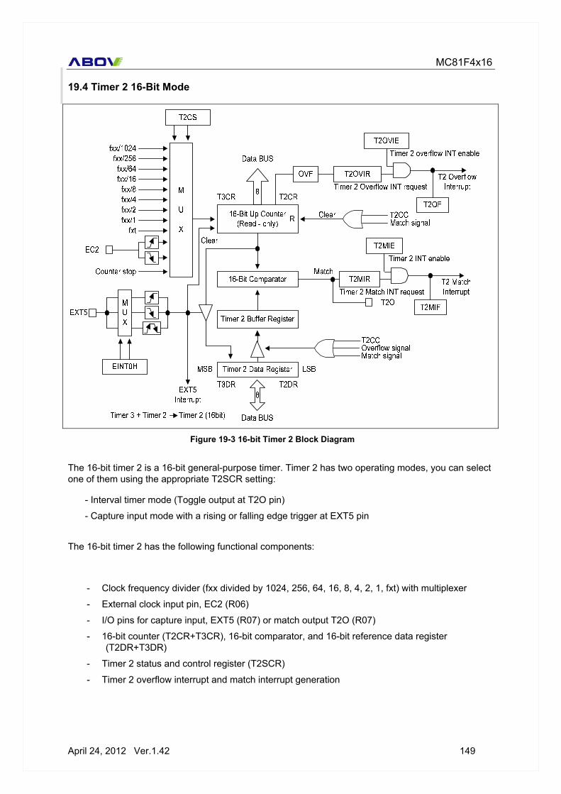
MC81F4x16
April 24, 2012 Ver.1.42 149
19.4 Timer 2 16-Bit Mode
The 16-bit timer 2 is a 16-bit general-purpose timer. Timer 2 has two operating modes, you can select one of them using the appropriate T2SCR setting:
- Interval timer mode (Toggle output at T2O pin)
- Capture input mode with a rising or falling edge trigger at EXT5 pin The 16-bit timer 2 has the following functional components:
- Clock frequency divider (fxx divided by 1024, 256, 64, 16, 8, 4, 2, 1, fxt) with multiplexer
- External clock input pin, EC2 (R06)
- I/O pins for capture input, EXT5 (R07) or match output T2O (R07)
- 16-bit counter (T2CR+T3CR), 16-bit comparator, and 16-bit reference data register (T2DR+T3DR)
- Timer 2 status and control register (T2SCR)
- Timer 2 overflow interrupt and match interrupt generation
Figure 19-3 16-bit Timer 2 Block Diagram

MC81F4x16
150 April 24, 2012 Ver.1.42
Function Description Interval Timer Mode A match signal is generated and T2O pins are toggled when the T2CR+T3CR register value equals the T2DR+T3DR. The match signal generates a timer match interrupt and clears the T2CR and the T3CR register. If, for example, you write the value 24H to T2DR, 10H to T3DR and 9FH to T2SCR, the counter will increment until it reaches 1024H. At this point, the Timer 0 math interrupt request is generated, the counter value is reset, and counting resumes. Capture Mode In capture mode, you have to set EXT5 interrupt. When the EXT5 interrupt is occurred, the T2CR and T2CR register value is loaded into the T2DR and T3DR register and the T2CR and T3CR register is cleared. And the timer 2 overflow interrupt is generated whenever the T2CR+T3CR value is overflowed. So, If you count how many overflow is occurred and read the T2DR+T3DR value in EXT5 interrupt routine, it is possible to measure the time between two EXT5 interrupts. Or it is possible to measure the time from the T2 initial time to the EXT5 interrupt occurred time. The time = (65536* tCLK ) * overflow_count + (tCLK * (T2CR+(T3DR<<8)))
Note ‘tCLK’ is the period time of the timer-counter’s clock source You must set the T2DR and T3DR values before set the T2SCR register. Because T2DR and T3DR values are fetched when the count is started(the T2CC bit is set) or match/overflow event is occurred.

MC81F4x16
April 24, 2012 Ver.1.42 151
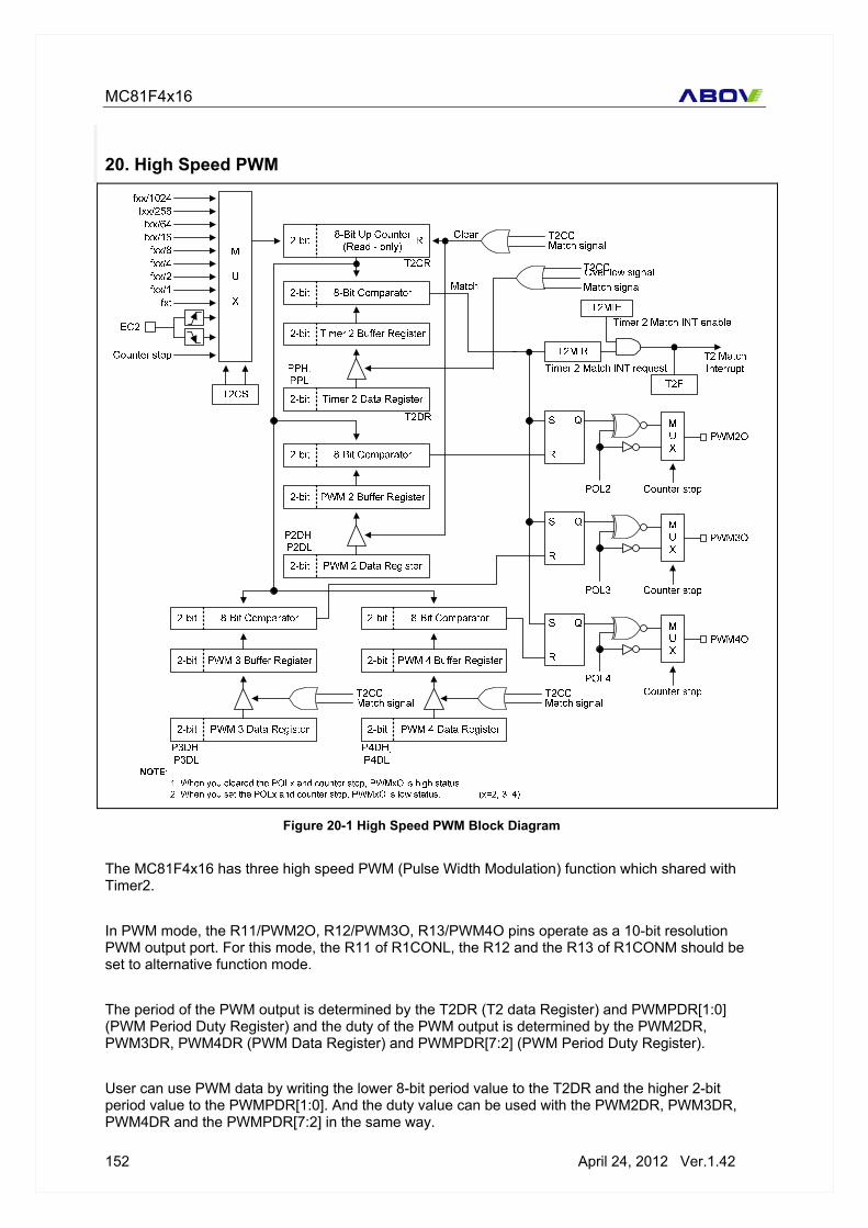
MC81F4x16
152 April 24, 2012 Ver.1.42
20. High Speed PWM
The MC81F4x16 has three high speed PWM (Pulse Width Modulation) function which shared with Timer2. In PWM mode, the R11/PWM2O, R12/PWM3O, R13/PWM4O pins operate as a 10-bit resolution PWM output port. For this mode, the R11 of R1CONL, the R12 and the R13 of R1CONM should be set to alternative function mode. The period of the PWM output is determined by the T2DR (T2 data Register) and PWMPDR[1:0] (PWM Period Duty Register) and the duty of the PWM output is determined by the PWM2DR, PWM3DR, PWM4DR (PWM Data Register) and PWMPDR[7:2] (PWM Period Duty Register). User can use PWM data by writing the lower 8-bit period value to the T2DR and the higher 2-bit period value to the PWMPDR[1:0]. And the duty value can be used with the PWM2DR, PWM3DR, PWM4DR and the PWMPDR[7:2] in the same way.
Figure 20-1 High Speed PWM Block Diagram

MC81F4x16
April 24, 2012 Ver.1.42 153
The bit POL2, POL3 and POL4 of PWMSCR decides the polarity of duty cycle. The duty value can be changed when the PWM outputs. However the changed duty value is output after the current period is over. And it can be maintained the duty value at present output when changed only period value shown as Example of PWM2. As it were, the absolute duty time is not changed in varying frequency.
Note : When user need to change mode from the Timer2 mode to the PWM mode, the Timer2 should be stopped firstly, and then set period and duty register value. If user writes register values and changes mode to PWM mode while Timer2 is in operation, the PWM data would be different from expected data in the beginning.
PWM Period = [PWMPDR[1:0]T2DR+1] X Source Clock PWM2 Duty = [PWMPDR[3:2]PWM2DR+1] X Source Clock PWM3 Duty = [PWMPDR[5:4]PWM3DR+1] X Source Clock PWM4 Duty = [PWMPDR[7:6]PWM4DR+1] X Source Clock If it needed more higher frequency of PWM, it should be reduced resolution.
Note : If the duty value and the period value are same, the PWM output is determined by the bit POL (1: High, 0: Low). And if the duty value is set to “00H”, the PWM output is determined by the bit POL(1: Low, 0: High). The period value must be same or more than the duty value, and 00H cannot be used as the period value.
Figure 20-2 Example of PWM2 at 8MHz

MC81F4x16
154 April 24, 2012 Ver.1.42
20.1 Registers
PWMSCR PWM STATUS AND CONTROL REGISTER (PWMSCR) 00CEH
7 6 5 4 3 2 1 0 PWMSCR POL4 POL3 POL2 PWMS – – – – Reset value: 0-H
R/W R/W R/W R/W – – – –
0: PWM 4 duty active low POL4 PWM 4 Polarity Selection Bit
1: PWM 4 duty active high 0: PWM 3 duty active low
POL3 PWM 3 Polarity Selection Bit 1: PWM 3 duty active high 0: PWM 2 duty active low
POL2 PWM 2 Polarity Selection Bit 1: PWM 2 duty active high 0: Timer 2 mode (interval or capture)
PWMS PWM Selection Bit 1: PWM mode (PWM2O, PWM3O, PWM4O )
– Bit3 – bit0 Not used for MC81F4x16
PWMPDR PWM PERIOD DUTY REGISTER 00CFH
7 6 5 4 3 2 1 0 PWMPDR P4DH P4DL P3DH P3DL P2DH P2DL PPH PPL Reset value: FFH
R/W R/W R/W R/W R/W R/W R/W R/W
P4DH PWM 4 Duty High Bit P4DL PWM 4 Duty Low Bit
PWM4 duty value ( 9,8th bits )
P3DH PWM 3 Duty High Bit P3DL PWM 3 Duty Low Bit
PWM3 duty value ( 9,8th bits )
P2DH PWM 2 Duty High Bit P2DL PWM 2 Duty Low Bit
PWM2 duty value ( 9,8th bits )
PPH PWM Period High Bit PPL PWM Period Low Bit
Period value ( 9/8th bits )
MC81F4x16
April 24, 2012 Ver.1.42 155
PWM2DR PWM 2 DATA REGISTER 00D0H
7 6 5 4 3 2 1 0 PWM2DR One byte register Reset value: FFH
R/W R/W R/W R/W R/W R/W R/W R/W
A 8-bit data register for lower bits of 10-bit PWM 2 duty value.
PWM3DR PWM 3 DATA REGISTER 00D1H
7 6 5 4 3 2 1 0 PWM3DR One byte register Reset value: FFH
R/W R/W R/W R/W R/W R/W R/W R/W
A 8-bit data register for lower bits of 10-bit PWM 3 duty value.
PWM4DR PWM 4 DATA REGISTER 00D2H
7 6 5 4 3 2 1 0 PWM4DR One byte register Reset value: FFH
R/W R/W R/W R/W R/W R/W R/W R/W
A 8-bit data register for lower bits of 10-bit PWM 4 duty value.

MC81F4x16
156 April 24, 2012 Ver.1.42
21. BUZZER
The buzzer driver consists of 8-bit binary counter, the buzzer period data register BUPDR, and the buzzer driver register BUZR, the clock selector. It generates square-wave which is very wide range frequency (244 Hz ~ 250 KHz at fxx = 8MHz) by user programmable counter. Pin R12/BUZO is assigned for output port of Buzzer driver by setting the bits R12 of R1 Control Middle Register (R0CONM) to “101”. The 8-bit buzzer counter is cleared and start the counting by writing signal to the register BUZR. It is increased from 00H until it matches with BUPDR[7:0]. Also, it is cleared by counter overflow and count up to output the square wave pulse of duty 50%. The bit 0 to 7 of BUPDR determines output frequency for buzzer driving. BUPDR is initialized to FFH after reset. Frequency calculation is following as shown below.
Figure 21-1 Buzzer Driver Block Diagram

MC81F4x16
April 24, 2012 Ver.1.42 157
21.1 Registers
BUZR BUZZER DRIVER REGISTER 00E5H
7 6 5 4 3 2 1 0 BUZR BUCK BUSS BURL – – – – Reset value: C-H
R/W R/W R/W R/W – – – –
00: fxt ( sub clock ) 01: fxx/16 10: fxx/32
BUCK Buzzer Clock Selection Bit
11: fxx/64 0: Disable Buzzer
BUSS Buzzer Start/Stop Bit 1: Enable Buzzer 0: No effect
BURL Buzzer Data Reload Bit 1: Reload buzzer data to buffer
– bit3 – bit1 Not used for MC81F4x16
BUPDR BUZZER PERIOD DATA REGISTER 00E6H
7 6 5 4 3 2 1 0 BUPDR One byte register Reset value: FFH
R/W R/W R/W R/W R/W R/W R/W R/W
A 8-bit data register for the buzzer period value.

MC81F4x16
158 April 24, 2012 Ver.1.42
21.2 Frequency table
System Clock = 4MHz BUCK :01 = div16
frequency unit = KHz
Low nibble of BUPDR High nibble 0 1 2 3 4 5 6 7
0 125.000 62.500 41.667 31.250 25.000 20.833 17.857 15.6251 7.353 6.944 6.579 6.250 5.952 5.682 5.435 5.208 2 3.788 3.676 3.571 3.472 3.378 3.289 3.205 3.125 3 2.551 2.500 2.451 2.404 2.358 2.315 2.273 2.232 4 1.923 1.894 1.866 1.838 1.812 1.786 1.761 1.736 5 1.543 1.524 1.506 1.488 1.471 1.453 1.437 1.420 6 1.289 1.276 1.263 1.250 1.238 1.225 1.214 1.202 7 1.106 1.096 1.087 1.078 1.068 1.059 1.050 1.042 8 0.969 0.962 0.954 0.947 0.940 0.933 0.926 0.919 9 0.862 0.856 0.850 0.845 0.839 0.833 0.828 0.822 A 0.776 0.772 0.767 0.762 0.758 0.753 0.749 0.744 B 0.706 0.702 0.698 0.694 0.691 0.687 0.683 0.679 C 0.648 0.644 0.641 0.638 0.635 0.631 0.628 0.625 D 0.598 0.595 0.592 0.590 0.587 0.584 0.581 0.579 E 0.556 0.553 0.551 0.548 0.546 0.543 0.541 0.539 F 0.519 0.517 0.514 0.512 0.510 0.508 0.506 0.504
Low nibble of BUPDR High nibble 8 9 A B C D E F
0 13.889 12.500 11.364 10.417 9.615 8.929 8.333 7.813 1 5.000 4.808 4.630 4.464 4.310 4.167 4.032 3.906 2 3.049 2.976 2.907 2.841 2.778 2.717 2.660 2.604 3 2.193 2.155 2.119 2.083 2.049 2.016 1.984 1.953 4 1.712 1.689 1.667 1.645 1.623 1.603 1.582 1.563 5 1.404 1.389 1.374 1.359 1.344 1.330 1.316 1.302 6 1.190 1.179 1.168 1.157 1.147 1.136 1.126 1.116 7 1.033 1.025 1.016 1.008 1.000 0.992 0.984 0.977 8 0.912 0.906 0.899 0.893 0.887 0.880 0.874 0.868 9 0.817 0.812 0.806 0.801 0.796 0.791 0.786 0.781 A 0.740 0.735 0.731 0.727 0.723 0.718 0.714 0.710 B 0.676 0.672 0.668 0.665 0.661 0.658 0.654 0.651 C 0.622 0.619 0.616 0.613 0.610 0.607 0.604 0.601 D 0.576 0.573 0.571 0.568 0.566 0.563 0.561 0.558 E 0.536 0.534 0.532 0.530 0.527 0.525 0.523 0.521 F 0.502 0.500 0.498 0.496 0.494 0.492 0.490 0.488
Ex ) BUPDR = 0xFC -> Freq = 0.494KHz
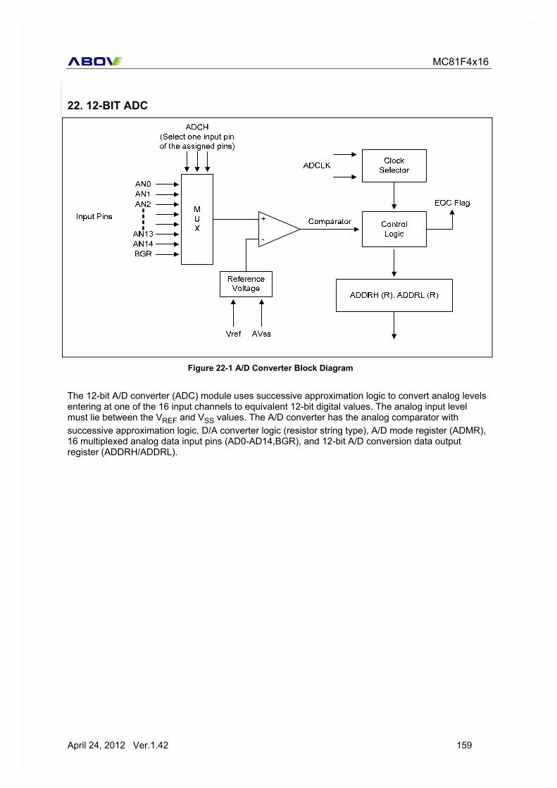
MC81F4x16
April 24, 2012 Ver.1.42 159
22. 12-BIT ADC
The 12-bit A/D converter (ADC) module uses successive approximation logic to convert analog levels entering at one of the 16 input channels to equivalent 12-bit digital values. The analog input level must lie between the VREF and VSS values. The A/D converter has the analog comparator with successive approximation logic, D/A converter logic (resistor string type), A/D mode register (ADMR), 16 multiplexed analog data input pins (AD0-AD14,BGR), and 12-bit A/D conversion data output register (ADDRH/ADDRL).
Figure 22-1 A/D Converter Block Diagram
MC81F4x16
160 April 24, 2012 Ver.1.42
22.1 Registers
ADMR A/D MODE REGISTER 00BDH
7 6 5 4 3 2 1 0 ADMR SSBIT EOC ADCLK ADCH Reset value: 00H
R/W R R/W R/W R/W R/W R/W R/W After reset, the start/stop bit is turned off. You can select only one analog input channel at a time. Other analog input (AD0-AD14,BGR) can be selected dynamically by manipulating the ADCH. And the pins not used for analog input can be used for normal I/O function.
0: Stop operation SSBIT Start or Stop bit
1: Start operation 0: Conversion not complete
EOC End of Conversion 1: Conversion complete
ADCLK A/D Clock Selection 00: fxx/1 01: fxx/2
10: fxx/4 11: fxx/8
ADCH A/D Input Pin Selection
0000: AN0 0001: AN1 0010: AN2 0011: AN3 0100: AN4 0101: AN5 0110: AN6 0111: AN7
1000: AN8 1001: AN9 1010: AN10 1011: AN11 1100: AN12 1101: AN13 1110: AN14 1111: BGR
ADDRH A/D CONVERTER DATA HIGH REGISTER 00BEH
7 6 5 4 3 2 1 0 ADDRH .11 .10 .9 .8 .7 .6 .5 .4 Reset value: XXH
R R R R R R R R
A 8-bit data register for higher 8-bits of the 12-bit ADC result.
ADDRL A/D CONVERTER DATA LOW REGISTER 00BFH
7 6 5 4 3 2 1 0 ADDRL .3 .2 .1 .0 - - - - Reset value: X-H
R R R R R R R R

MC81F4x16
April 24, 2012 Ver.1.42 161
A 8-bit data register for lower 4-bits of the 12-bit ADC result.
22.2 Procedure
To do the A/D converting, follow these basic steps: 1. Set the ADC pins as the alternative mode. 2. Set the ADMR register for
- setting ADC channel - setting Clock - clearing the ‘End of Conversion’ bit - starting ADC
3. Wait until ADC is finished ( check the ‘End of Conversion’ bit ) When ADC is finished, EOC bit is set and SSBIT is cleared automatically.
4. Read the ADCRH and ADCRL register To initiate an analog-to-digital conversion procedure, at first you must set ADC pins to alternative function (ADC analog input) mode. And you write the channel selection data in the A/D mode register (ADMR) to select one of analog input channels and set the conversion start/stop bit, SSBIT. The pins not used for ADC can be used for normal I/O. To start the A/D conversion, you should set the start/stop bit, SSBIT. When a conversion is completed, the end-of-conversion bit, EOC is automatically set to 1 and the result is dumped into the ADDRH/ADDRL register. Then the A/D converter enters an idle state. The EOC bit is cleared when SSBIT is set. Note that, ADC interrupt is not provided.
Note : Because the A/D converter has no sample-and-hold circuitry, it is very important that fluctuation of the analog level at the ADC input pins during a conversion procedure be kept to an absolute minimum. Any change in the input level, perhaps due to noise, will invalidate the result. If the chip enters to STOP or IDLE mode in conversion process, there will be a leakage current path in A/D block. You must use STOP or IDLE mode after ADC operation is finished.
22.3 Conversion Timing
The A/D conversion process requires 4 steps (4 clock edges) to convert each bit and 10 clocks to set-up A/D conversion. Therefore, total of 66 clocks are required to complete a 12-bit conversion: When fxx/8 is selected for conversion clock with a 12 MHz fxx clock frequency, one clock cycle is 0.66 μs. Each bit conversion requires 4 clocks, the conversion rate is calculated as follows: 4 clocks/bit × 14 bits + set-up time = 66 clocks, 66 clock × 0.66 μs = 44.0 μs at 1.5 MHz (12 MHz/8)
Note : The A/D converter needs at least 25 μs for conversion time. So you must set the conversion time slower than 25 μs.
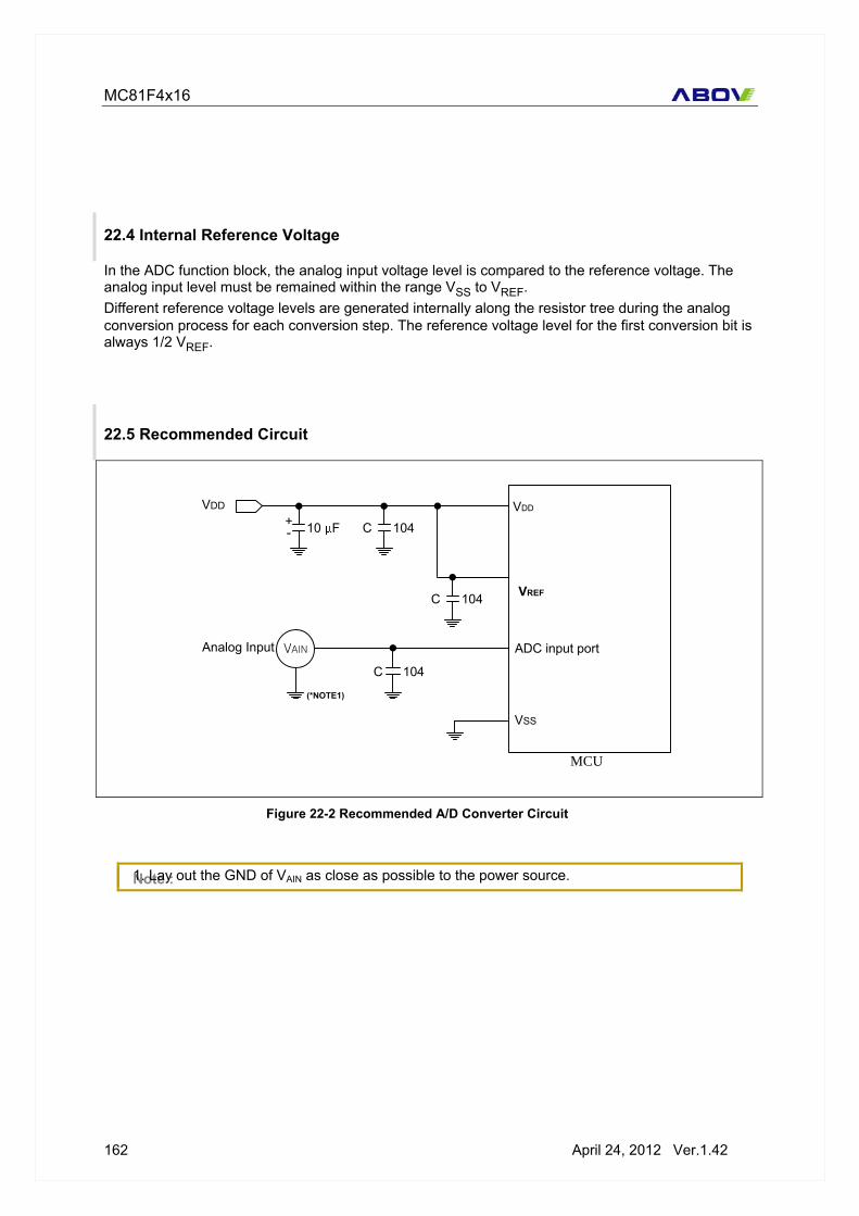
MC81F4x16
162 April 24, 2012 Ver.1.42
22.4 Internal Reference Voltage
In the ADC function block, the analog input voltage level is compared to the reference voltage. The analog input level must be remained within the range VSS to VREF. Different reference voltage levels are generated internally along the resistor tree during the analog conversion process for each conversion step. The reference voltage level for the first conversion bit is always 1/2 VREF.
22.5 Recommended Circuit
VSS
MCU
ADC input portAnalog Input
10 F 104C
104C
+-
VDD
VREF
VDD
VAIN
(*NOTE1)
104C
Note : 1. Lay out the GND of VAIN as close as possible to the power source.
Figure 22-2 Recommended A/D Converter Circuit

MC81F4x16
April 24, 2012 Ver.1.42 163
23. SERIAL I/O INTERFACE
Serial I/O interface modules, SIO can interface with various types of external device that require serial data transfer. The components of SIO function block are:
- 8-bit control register (SIOCR)
- Clock selector logic
- 8-bit data register (SIODAT)
- 8-bit pre-scaler register (SIOPS)
- 3-bit clock counter
- Serial data I/O pins (SI, SO)
- Serial clock pin (SCK)
The SIO module can transmit or receive 8-bit serial data at a frequency determined by its corresponding control register settings. To ensure flexible data transmission rates, you can select internal or external clock source.
Figure 23-1 SIO Block Diagram
MC81F4x16
164 April 24, 2012 Ver.1.42
23.1 Registers
SIOCR SERIAL I/O INTERFACE CONTROL REGISTER 00E7H A reset clears the SIOCR register value to "00H". With this value, internal clock source and receive-only mode are selected and the 3-bit counter is cleared. The data shift operation is disabled. The selected data direction is MSB-first.
7 6 5 4 3 2 1 0 – – CSEL DAT SIOM SIOP CCLR SEDGE SIOCR – – R/W R/W R/W R/W R/W R/W
Reset value: --00_0000b
– bit7 – bit6 Not used for MC81F4432
0: Internal clock (P.S clock) CSEL SIO Shift Clock Selection Bit
1: External clock (SCK) 0: MSB-first mode
DAT Data Direction Control Bit 1: LSB-first mode 0: Receive only mode
SIOM SIO Mode Selection Bit 1: Transmit/Receive mode 0: Disable shifter and clock counter
SIOP SIO Shift Operation Enable Bit 1: Enable shifter and clock counter 0: No action
CCLR SIO Counter Clear and Shift Start Bit 1: Clear 3-bit counter and start shifting 0: Tx at falling edges, Rx at rising edges
SEDGE Shift Clock Edge Selection Bit 1: Tx at rising edges, Rx at falling edges
SIODAT SIO DATA REGISTER 00E8H
7 6 5 4 3 2 1 0 SIODAT One byte register Reset value: 00H
R/W R/W R/W R/W R/W R/W R/W R/W
A 8-bit data register for SIO Rx/Tx data
SIOPS SIO PRE-SCALER REGISTER 00E9H
7 6 5 4 3 2 1 0 SIOPS One byte register Reset value: 00H
R/W R/W R/W R/W R/W R/W R/W R/W
MC81F4x16
April 24, 2012 Ver.1.42 165
Baud rate = (fxx/4) / (SIOPS+1)
23.2 Procedure
To program the SIO module, follow these basic steps: 1. Configure the I/O pins at port (SCK/SI/SO) by loading the appropriate value to the R0CONM, R0CONH register if necessary. - If one side uses a internal clock, the other side must use a external clock. - Note that, if the external clock is used, you must set the SCK port as an input mode. 2. Set SIOPS register with proper pre-scale value. 3. Load an 8-bit value to the SIOCR to properly configure the serial I/O module. In this operation, SIOP [SIOCR.2] bit must be set to "1" to enable the data shifter. 4. For interrupt generation, set the SIO interrupt enable bit, SIOIE to "1". 5. Data transmit and receiving are occurred at the same time. So before start the shift operation, you must set the SIODAT with what you want to transmit. - When SIOM [SIOCR.3] bit is 0, it does not transmit a data. 6. When set SIOCR.1 to 1, the shift operation starts. - With internal clock: shift operation is started right after SIOCR.1 is set. - With external clock: shift operation is started when the master starts the operation. 7. When the shift operation (transmit/receive) is completed, the SIO interrupt request flag bit, SIOIR is set to "1" and SIO interrupt request is generated. - Don’t forget to set the SIOCR.1 bit by 1, to receive next SIO data if want. When the SIO interrupt sub-routine is serviced, the SIO interrupt request flag bit, SIOIR, is cleared automatically.

MC81F4x16
166 April 24, 2012 Ver.1.42
24. UART
The UART block has four communication modes. One synchronous mode and three UART (Universal Asynchronous Receiver/Transmitter) modes.
- Mode 0 : Serial I/O with baud rate of fxx/(16 × (BRDAT+1)) half-duplex and master mode only
- Mode 1 : 8-bit UART mode; variable baud rate : no parity bit - Mode 2 : 9-bit UART mode; fxx/16 - Mode 3 : 9-bit UART mode, variable baud rate
Figure 24-1 UART Block Diagram

MC81F4x16
April 24, 2012 Ver.1.42 167
24.1 Registers
UCONH UART CONTROL HIGH REGISTER (UCONH) 00FCH When current mode is 2 or 3, and the ‘MCE’ bit is enabled, Rx interrupt is generated when only 9th bit of Rx data is ‘1’. This feature is used to Multiprocessor Communication. See ‘24.4 Muti-processor Communication’ on page 175 for more detail information. In mode 1, and the ‘MCE’ bit is enabled, Rx interrupt is generated when only valid stop bit is received. In mode 0, the ‘MCE’ bit must be ‘0’. TB8 and RB8 bits are ignored when current mode is 0 or 1, or the ‘UTP(UCONL.7 / UART parity auto-generation)’ bit is enabled.
7 6 5 4 3 2 1 0 UCONH UMS1 UMS0 MCE SDR TB8 RB8 – – Reset value: 00H
R/W R/W R/W R/W R/W R/W – –
00: Mode 0; Synchronous mode (fu/(16×(BRDAT+1)))
01: Mode 1; 8-bit UART (fu/(16×(BRDAT+1)))
10: Mode 2; 9-bit UART (fxx/16)
UMS UART Mode Selection Bits
11: Mode 3; 9-bit UART (fu/(16×(BRDAT+1)))
0: Disable MCE Multiprocessor Communication Enable Bit
(for modes 2 and 3 only) 1: Enable 0: Receive Disable
SDR Serial Data Receive Enable Bit 1: Receive Enable
TB8 TB8 9th bit of Tx Data
RB8 RB8 9th bit of Rx Data
– bit1 – bit0 Not used for MC81F4x16
Note : ‘fu’ is the clock source which is selected by the UCLK(UCONL.[2-3]) bits.

MC81F4x16
168 April 24, 2012 Ver.1.42
UCONL UART CONTROL LOW REGISTER 00FDH
7 6 5 4 3 2 1 0 UCONL UTP UTPS URPS URPER UCLK – – Reset value: 00H
R/W R/W R/W R/W R/W R/W – –
0: Disable parity-bit auto-generation UTP UART Transmit Parity-bit
Auto-Generation Enable Bit 1: Enable parity-bit auto-generation 0: Even parity-bit
UTPS UART Transmit Parity-bit Selection Bit (for modes 2 and 3 only) 1: Odd parity-bit
0: Even parity-bit check URPS
UART Receive Parity-bit Selection Bit (for modes 2 and 3 only) 1: Odd parity-bit check
0: No parity-bit error URPER
UART Receive Parity-bit Error Status Bit (for modes 2 and 3 only) 1: Parity-bit error
00: fxx/8 01: fxx/4 10: fxx/2
UCLK UART Clock Selection Bits
11: fxx/1 – bit1 – bit0 Not used for MC81F4x16
UDAT UART DATA REGISTER 00FEH Both UART receive and transmit buffers are both accessed via the UDAT register even two buffers are physically separated. Writing to the UDAT register accesses the transmit buffer; reading the UDAT register accesses the receive buffer.
7 6 5 4 3 2 1 0 UDAT One byte register Reset value: XXH
R/W R/W R/W R/W R/W R/W R/W R/W
A 8-bit data register for UART Rx/Tx data
BRDAT UART BAUD RATE DATA REGISTER 00FFH
7 6 5 4 3 2 1 0 BRDAT One byte register Reset value: FFH
R/W R/W R/W R/W R/W R/W R/W R/W
A 8-bit data register for UART baud rate setting

MC81F4x16
April 24, 2012 Ver.1.42 169
24.2 Modes and Procedures
Uart Mode 0
In mode 0, both input and output data are passed through the RxD (R14) pin and TxD (R15) pin generates the clock. Data is transmitted or received in 8-bit units only. The LSB of the 8-bit value is transmitted (or received) first. Note that, only master mode is provided.
Figure 24-2 Timing Diagram for Serial Port Mode 0 Operation

MC81F4x16
170 April 24, 2012 Ver.1.42
Mode 0 Transmit Procedure 1. Set Rx/Tx pins to Alternative mode. 2. Set the baud rate
- Select the UART clock by setting the UCLK(UCONL.[3-2]) bits. - Set the BRDAT register properly
3. Select mode 0 by setting the USM(UCONH.[7-6]) bits. 4. Write transmission data to the UDA. After finish above steps, the data transmission will be started. And after finish the transmission, both UTIR(IRQL.3) and UTIF(INTFL.0) bits are set to ‘1’ by hardware. Mode 0 Receive Procedure 1. Set the baud rate
- Select the UART clock by setting the UCLK(UCONL.[3-2]) bits. - Set the BRDAT register properly
2. Select mode 0 by setting the USM(UCONH.[7-6]) bits. 3. Clear the receive interrupt request flag bit URIR(IRQL.4). 4. Set the SDR(UCONH.4 / UART receive enable bit) by ‘1’.
Right after finish above steps, the shift clock will be output to the TxD (R15) pin and receiving is started at the RxD (R14) pin. After finish receiving, both URIR(IRQL.4) and URIF(INTFL.1) bits are set to "1" by hardware.
Uart Mode 1

MC81F4x16
April 24, 2012 Ver.1.42 171
In mode 1, 10-bits are transmitted (through the TxD (R15) pin) or received (through the RxD (R14) pin). Each data frame has three components:
- Start bit ("0") - 8 data bits (LSB first) - Stop bit ("1")
* The baud rate for mode 1 is variable depend on the BRDAT register value. * Parity bit is not available for mode 1.( mode 2,3 provide parity bit ) Mode 1 Transmit Procedure 1. Set Rx pin to input mode and Tx pin to alternative mode. 2. Set the baud rate
- Select the UART clock by setting the UCLK(UCONL.[3-2]) bits. - Set the BRDAT register properly
3. Select mode 1 by setting the USM(UCONH.[7-6]) bits. 4. Write transmission data to the UDAT.
After finish above steps, the data transmission will be started. And after finish the transmission, the UTIR(IRQL.3) bit is set to ‘1’ by hardware. Mode 1 Receive Procedure 1. Set Rx pin to input mode and Tx pin to alternative mode. 2. Set the baud rate
- Select the UART clock by setting the UCLK(UCONL.[3-2]) bits. - Set the BRDAT register properly
3. Select mode 1 by setting the USM(UCONH.[7-6]) bits and set the SDR (UCONH.4 / Receive Enable) bit in the UCONH register to "1".
After finish above steps, the receive operation starts when the signal at the RxD (R14) pin goes to low level( start bit ). After finish receiving, the URIR(IRQL.4) is set to "1".
Figure 24-3 Timing Diagram for UART Mode 1 Operation

MC81F4x16
172 April 24, 2012 Ver.1.42
Uart Mode 2 / 3
The mode 2 is exactly same with mode 3 when the BRDAT register value is ‘00h’. In mode 2 the BRDAT is assumed ‘00h’ even whatever value is stored in the BRDAT register. But in mode 3, the baud rate is changeable by the BRDAT register. In mode 2 and 3, 11-bits are transmitted (through the TxD (R15) pin) or received (through the RxD (R14) pin). Each data frame has four components:
- Start bit ("0") - 8 data bits (LSB first) - Programmable 9th data bit - Stop bit ("1")
The 9th data bit to be transmitted can be assigned a value of "0" or "1" by writing the TB8(UCONH.3) bit. When receiving, the 9th data bit that is received is written to the RB8(UCONH.2) bit, while the stop bit is ignored. The baud rate for mode 2 is fu/16 (BRDAT is ignored in mode 2). The baud rate for mode 3 is fu/(16×(BRDAT+1)).
Figure 24-4 Timing Diagram for UART Mode 2 and 3 Operation

MC81F4x16
April 24, 2012 Ver.1.42 173
Mode 2 / 3 Transmit Procedure 1. Set Rx pin to input mode and Tx pin to alternative mode. 2. Set the baud rate
- Select the UART clock by setting the UCLK(UCONL.[3-2]) bits. - Set the BRDAT register properly( in mode 3 only )
3. Select mode 2 or 3 by setting the USM(UCONH.[7-6]) bits. 4. Set the 9th bit, there are two way to set the 9th bit.
- Set the ‘UTP(UCONL.7 / parity auto-generatio)’ bit by ‘1’ - Or, Clear ‘UTP(UCONL.7 / parity auto-generation)’ bit by ‘0’ and write the 9th bit data to the TB8(UCONH.3) bit as you want.
5. Write transmission data to the UDAT. After finish above steps, the data transmission will be started. And after finish the transmission, the UTIR(IRQL.3) bit is set to ‘1’ by hardware. Mode 2 / 3 Receive Procedure 1. Set Rx pin to input mode and Tx pin to alternative mode. 2. Set the baud rate
- Select the UART clock by setting the UCLK(UCONL.[3-2]) bits. - Set the BRDAT register properly( in mode 3 only )
3. Select mode 2 or 3 by setting the USM(UCONH.[7-6]) bits. 4. If you want, set the MCE(UCONH.5 / multi-processor communication enable) bit
If you do not want the MCE feature, do not have to set the MCE bit. 5. Set the SDR(UCONH.4 / receive enable) bit by ‘1’. 6. After finish above steps, the receive operation starts when the signal at the RxD (R14) pin goes to low level( start bit ). After finish receiving, the URIR(IRQL.4) is set to "1".
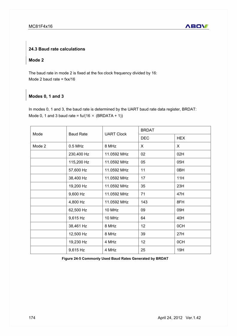
MC81F4x16
174 April 24, 2012 Ver.1.42
24.3 Baud rate calculations
Mode 2 The baud rate in mode 2 is fixed at the fxx clock frequency divided by 16: Mode 2 baud rate = fxx/16
Modes 0, 1 and 3 In modes 0, 1 and 3, the baud rate is determined by the UART baud rate data register, BRDAT: Mode 0, 1 and 3 baud rate = fu/(16 × (BRDATA + 1))
BRDAT Mode Baud Rate UART Clock
DEC HEX
Mode 2 0.5 MHz 8 MHz X X
230,400 Hz 11.0592 MHz 02 02H
115,200 Hz 11.0592 MHz 05 05H
57,600 Hz 11.0592 MHz 11 0BH
38,400 Hz 11.0592 MHz 17 11H
19,200 Hz 11.0592 MHz 35 23H
9,600 Hz 11.0592 MHz 71 47H
4,800 Hz 11.0592 MHz 143 8FH
62,500 Hz 10 MHz 09 09H
9,615 Hz 10 MHz 64 40H
38,461 Hz 8 MHz 12 0CH
12,500 Hz 8 MHz 39 27H
19,230 Hz 4 MHz 12 0CH
9,615 Hz 4 MHz 25 19H
Figure 24-5 Commonly Used Baud Rates Generated by BRDAT

MC81F4x16
April 24, 2012 Ver.1.42 175
24.4 Muti-processor Communication
The MC81F4x16 multiprocessor communication features lets a "master" device send a multiple-frame serial message to a "slave" device in a multi-processor configuration. It does this without interrupting other slave devices that may be on the same serial line. This feature can be used only in UART modes 2 or 3. In these modes 2 and 3, 9 data bits are received. The 9th bit value is written to RB8 (UCONH.2). The data receive operation is concluded with a stop bit. You can program this function so that when the stop bit is received, the serial interrupt will be generated only if RB8 = "1". To enable this feature, you set the MCE bit in the UCONH register. When the MCE bit is "1", serial data frames that are received with the 9th bit = "0" do not generate an interrupt. In this case, the 9th bit simply separates the address from the serial data. Sample Protocol for Master/Slave Interaction When the master device wants to transmit a block of data to one of several slaves on a serial line, it first sends out an address byte to identify the target slave. Note that in this case, an address byte differs from a data byte: In an address byte, the 9th bit is "1" and in a data byte, it is "0". The address byte interrupts all slaves so that each slave can examine the received byte and see if it is being addressed. The addressed slave then clears its MCE bit and prepares to receive incoming data bytes. The MCE bits of slaves that were not addressed remain set, and they continue operating normally while ignoring the incoming data bytes. While the MCE bit setting has no effect in mode 0, it can be used in mode 1 to check the validity of the stop bit. For mode 1 reception, if MCE is "1", the receive interrupt will be issue unless a valid stop bit is received.
Figure 24-6 Connection Example for Multiprocessor Serial Data Communications
TxD RxD MASTER
RxD TxD Slave 1
RxD TxD Slave 1
RxD TxD Slave N

MC81F4x16
176 April 24, 2012 Ver.1.42
Setup Procedure for Multiprocessor Communications Follow these steps to configure multiprocessor communications:
1. Set all MC81F4x16 devices (masters and slaves) to UART mode 2 or 3. 2. Write the MCE bit of all the slave devices to "1". 3. The master device's transmission protocol is:
- First byte: the address identifying the target slave device (9th bit = "1") - Next bytes: data (9th bit = "0")
4. When the target slave receives the first byte, all of the slaves are interrupted because the 9th data bit is "1". The targeted slave compares the address byte to its own address and then clears its MCE bit in order to receive incoming data. The other slaves continue operating normally.
24.5 Interrupt
Interrupt Timing In mode 0, the URIR(IRQL.4) bit is set to "1" when the 8th receive data bit has been shifted. In mode 1, the URIR(IRQL.4) bit is set to "1" at the halfway point of the stop bit's shift time. In mode 2, or 3, the URIR(IRQL.4) bit is set to "1" at the halfway point of the RB8 bit's shift time. When the CPU has acknowledged the receive interrupt request flag condition, the URIR(IRQL.4) bit is cleared automatically. In mode 0, the UTIR(IRQL.3) bit is set to "1" when the 8th transmit data bit has been shifted. In mode 1, 2, or 3, the UTIR(IRQL.3) bit is set at the start of the stop bit. When the CPU has acknowledged the transmit interrupt request flag condition, the UTIR(IRQL.3) 4 bit is cleared automatically. Shared Interrupt Vector In case of using interrupts of UART Tx and UART Rx together, it is necessary to check UTIF and URIF in interrupt service routine to find out which interrupt is occurred, because the UART Tx and UART Rx is shared with the same interrupt vector address. These flag bits must be cleared by software after reading this register. ( UTIF and URIF are placed in INTFL register. See ‘9.6 Control Registers ( SFR )’ on page 71)

MC81F4x16
April 24, 2012 Ver.1.42 177
25. SLAVE IIC IIC is used to communicate between some devices with 2 lines which are SDA(Serial Data Line) and SCL(Serial Clock Line). Both two lines are bidirectional open drain lines which are pulled up with registers. IIC provides ‘standard mode’ (max 100Kbps) and ‘fast mode’ (max 400Kbps).
25.1 Roles
There are two roles in an IIC communication. Which are ‘master’ and ‘slave’.
- Master : that generates the clock and transfer slave’s address. - Slave : that receives the clock and matched with message’s slave address.
Note: MC81F4x16 provides the slave mode only.
25.2 Registers
Address Register(IICAR)
SCLIIC-Bus
Control Logic(IICSCR)
Compare
Data Shifter(IICDSR) SDA
Interrupt
Data Bus
Figure 25-1 Registers for IIC
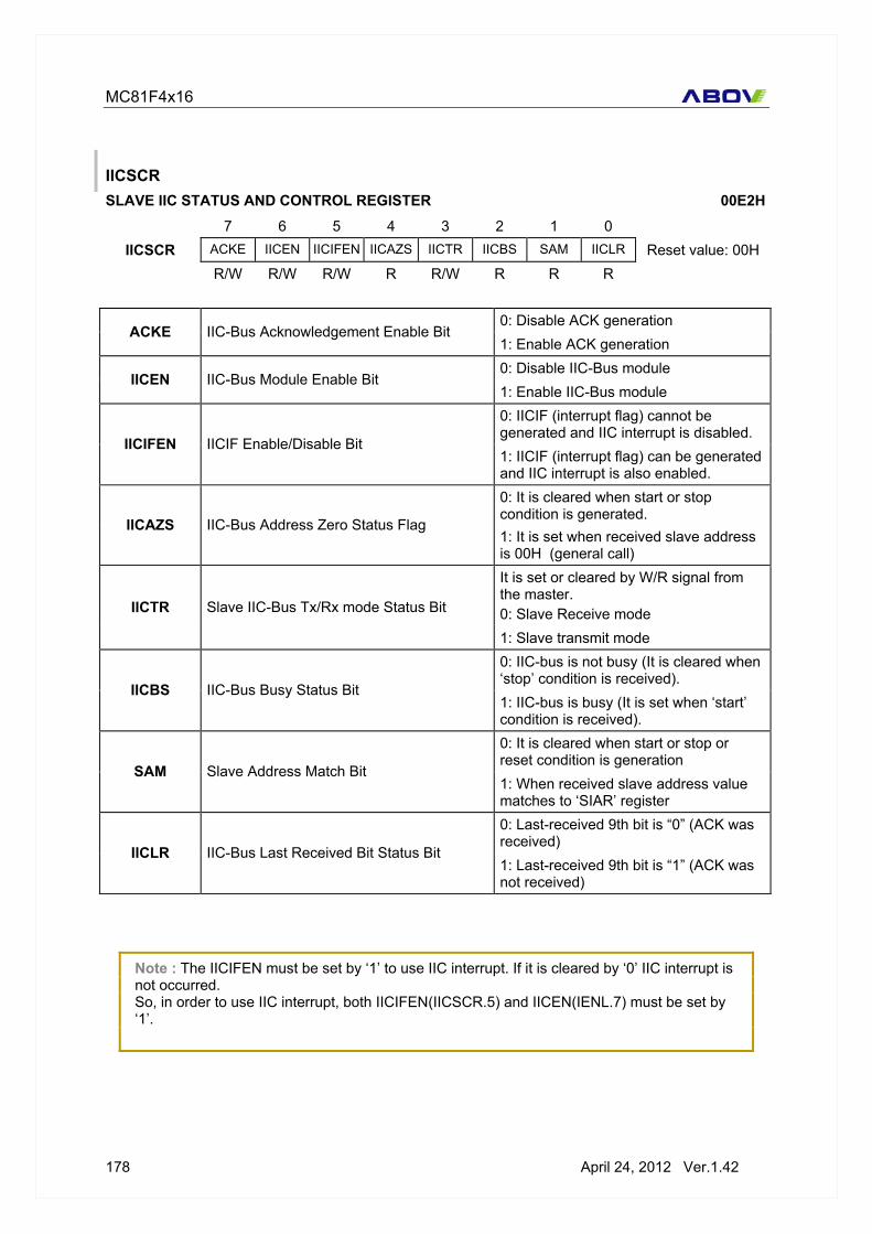
MC81F4x16
178 April 24, 2012 Ver.1.42
IICSCR SLAVE IIC STATUS AND CONTROL REGISTER 00E2H
7 6 5 4 3 2 1 0 IICSCR ACKE IICEN IICIFEN IICAZS IICTR IICBS SAM IICLR Reset value: 00H
R/W R/W R/W R R/W R R R
0: Disable ACK generation ACKE IIC-Bus Acknowledgement Enable Bit
1: Enable ACK generation 0: Disable IIC-Bus module
IICEN IIC-Bus Module Enable Bit 1: Enable IIC-Bus module 0: IICIF (interrupt flag) cannot be generated and IIC interrupt is disabled.
IICIFEN IICIF Enable/Disable Bit 1: IICIF (interrupt flag) can be generated and IIC interrupt is also enabled. 0: It is cleared when start or stop condition is generated.
IICAZS IIC-Bus Address Zero Status Flag 1: It is set when received slave address is 00H (general call) It is set or cleared by W/R signal from the master. 0: Slave Receive mode IICTR Slave IIC-Bus Tx/Rx mode Status Bit
1: Slave transmit mode 0: IIC-bus is not busy (It is cleared when ‘stop’ condition is received).
IICBS IIC-Bus Busy Status Bit 1: IIC-bus is busy (It is set when ‘start’ condition is received). 0: It is cleared when start or stop or reset condition is generation
SAM Slave Address Match Bit 1: When received slave address value matches to ‘SIAR’ register 0: Last-received 9th bit is “0” (ACK was received)
IICLR IIC-Bus Last Received Bit Status Bit 1: Last-received 9th bit is “1” (ACK was not received)
Note : The IICIFEN must be set by ‘1’ to use IIC interrupt. If it is cleared by ‘0’ IIC interrupt is not occurred. So, in order to use IIC interrupt, both IICIFEN(IICSCR.5) and IICEN(IENL.7) must be set by ‘1’.

MC81F4x16
April 24, 2012 Ver.1.42 179
IICDSR IIC DATA SHIFT REGISTER 00E4H
7 6 5 4 3 2 1 0 IICDSR One byte register Reset value: XXH
R/W R/W R/W R/W R/W R/W R/W R/W
When only IICSCR.6=’1’, write operation is enabled. But read operation is possible at anytime, regardless of the current IICSCR.6 bit setting.
A 8 bit register for Tx/Rx data of slave IIC. Note that, When only the IICEN(IICSCR.6) bit is enabled, writing to the ‘IICAR’ is available.
But reading is possible anytime, regardless of the current IICEN(IICSCR.6) bit status.
IICAR IIC ADDRESS REGISTER 00E3H
7 6 5 4 3 2 1 0 IICAR 7 bits address data - Reset value: XXH
R/W R/W R/W R/W R/W R/W R/W R/W
A 8 bit register for the 7 bit slave address. Note that, When only the IICEN(IICSCR.6) bit is disabled, writing to the ‘IICAR’ is available.
But reading is possible anytime, regardless of the current IICEN(IICSCR.6) bit status.

MC81F4x16
180 April 24, 2012 Ver.1.42
25.3 Message format
START, Repeated START and STOP One IIC data message is started by ‘START condition’ and finished by ‘STOP’ or ‘START’ condition. If one message is finished by ‘START’ condition, it means both an end of the current message and a start of the next message at the same time. So we call it ‘repeated START condition’. Repeated START is used to keep the IIC communication bus. If master transmit the STOP condition, other masters can take the bus. To prevent it, the repeated START condition is used. When SDA(data line) is changed while SCL(clock line) is staying high, it must be one of START, repeated Start or STOP condition. In other words, changing SDA state while SCL is staying high is not possible except those conditions.
START : SDA is changed from HIGH to LOW while SCL is staying high. STOP : SDA is changed from LOW to HIGH while SCL is staying high. Repeated START : START condition at the end of the frame.
Message Transmit After START or repeated START condition, one byte data is transferred from master to slave. The first one byte data consist of 7 bit address and 1 bit read/write flag. And 1 bit ACK(acknowledge) is transferred from slave to master to notice that receiving process is correctly finished and the slave address is matched.
Note: Simply transmitting ‘0’ is ACK.
After then, one or more data bytes are transferred. The data bytes are sent MSB first. It is possible both master to slave and slave to master based on the read/write bit flag (the last bit of the first one byte).
Write = read/write bit is 0 = data is transferred from master to slave.
Figure 25-2 Data transfer on the IIC-BUS

MC81F4x16
April 24, 2012 Ver.1.42 181
Read = read/write bit is 1 = data is transferred from slave to master. After each data bytes are transferred, ACK can be transferred from receiver. But meaning is different based on situation.
- Write time : master transmit and slave receive, slave transmit a ACK when one byte data is correctly received. So, slave must transmit a ACK when receive is finished.
- Read time : slave transmit and slave receive, master transmit a ACK when there are more bytes to transmit. So, if there is no more data to transmit, master dose not transmit a ACK.
1 Bit Transmit
The data bytes and ACK are consist of one bit transmits. If SDA is not changed while SCL is staying high, SDA status is one bit data. As already said, If SDA is changed while SCL is staying high, it is START or STOP condition. Therefore, transfer device change the SDA status while SCL is staying low. And when SCL is going to low, 1 bit transmit is finished. 1 bit data value and state are,
1 : high state ( more preciously said, line is open-drained and pulled up ). 0 : low state
Figure 25-3 Acknowledge on the IIC-BUS
Figure 25-4 Bit transfer on the IIC-BUS

MC81F4x16
182 April 24, 2012 Ver.1.42
25.4 Procedure
Initialization Following steps initialize the IIC slave. 1. Set SCL and SDA pins as an alternative mode.
Set the R1CONH[7~4] bits by “1010b”. 2. Set the slave address by setting the IICAR register. 3. Enable IIC module and the interrupt :
Set the ACKE bit by ‘1’ Set the IICEN bit by ‘1’ Set the IICIFEN bit by ‘1’. ( If it is cleared by ‘0’, IIC interrupt is not occurred ) -> Or you can simply set the IICSCR register by ‘E0h’.
After finish above steps, IIC interrupt is enabled. So The IIC interrupt will be generated after receive or transmit one byte.
Interrupt Routine Procedure Simply say, when you write a byte to the IICSCR, it is transmitted and when a byte is received, you can read it from the IICDSR register. But, the master has a right to decide the read/write mode. And the master sends 1-bit R/W mode flag after 7-bit slave address. And it is stored in the IICTR(IICSCR.3) bit when it is received. So you can recognize current Rx/Tx mode. And you have to react based on the IICTR(IICSCR.3) bit. The IICTR(IICSCR.3) bit equals ‘1’ means that the master want to read from the slave. So, In this case, Slave-IIC’s mode is changed into ‘transmit mode’ automatically. So, in this case you have to write a data to the IICDSR register as you want. The IICTR(IICSCR.3) bit equals ‘0’ means that the master want to write to the slave. So, In this case, Slave-IIC’s mode is changed into ‘receive mode’ automatically. So, in this case you have to read a data from the IICDSR register. Before finish the IIC interrupt routine, you have to clear the IICIF bit. When the IICIF bit is cleared, the SCL line is released. If it is not cleared, the SCL line is holding down to low status. While in this condition, master can’t continue the IIC communication. In order to recognize current received byte’s position in the message, you have to count the IIC interrupts. Based on the position information
Figure 25-5 IIC Salve Receiving Timing Diagram

MC81F4x16
April 24, 2012 Ver.1.42 183
Figure 25-6 IIC Slave Transmit Timing Diagram

MC81F4x16
184 April 24, 2012 Ver.1.42
26. RESET
26.1 Reset Process
When the reset event is occurred, there is a ‘stabilization time’ at the beginning. This time is counted from 00h to FFh by BIT. So it takes 1/(fxin/1024) * 256 second. After that, the ‘reset process step’ is started. It takes 6 system clock time. At this time, following statuses are initialized.
On- chip Hardware Initial Value
Program Counter ( PC ) high byte = a byte at FFFFh low byte = a byte at FFFEh FFFFh and FFFEh stores the reset vector.
RAM Page Register ( PRP ) 0
G-flag ( G ) 0
Operation Mode OSCS setting of Rom option
Control registers Initialized by reset values (See ‘9.6 Control Registers ( SFR )’ on page 71)
Low Voltage Reset LVREN setting of Rom option
After that, the main program execution is started from the reset vector address which is stored at FFFFh and FFFFEh.
Figure 26-1 Timing Diagram After Reset
26-1 Initializing Status by Reset

MC81F4x16
April 24, 2012 Ver.1.42 185
26.2 Reset Sources
There are four reset sources in MC81F4x16. Those are external reset, watch dog timer reset, power on reset and low voltage reset.
26.3 Reset circuit
When the external reset is enabled and the input signal of RESET pin is going to low for a while and going to high, the external reset is occurred.( See ‘7.7 Serial I/O Characteristics’ on page 46 for more timing information.) The Reset Pin should be pulled up to VDD with 75kohm resistor, if reset pin voltage is higher than VDD over 2V gap, MCU process self test procedure It is possible to use a Reset pin like Figure 26-3..
external reset application
general purpose I/O application
Figure 26-2 Reset Sources Diagram

MC81F4x16
186 April 24, 2012 Ver.1.42
26.4 Watch Dog Timer Reset
See ‘16. WATCH DOG TIMER’ on page 125.
Figure 26-3 Reset circuit Example

MC81F4x16
April 24, 2012 Ver.1.42 187
26.5 Power On Reset
There is a internal power on reset circuit internally. We simply call it POR. POR occurs the reset event when VDD is rising over the POR level. Note that, POR can be enabled and disabled by the PORC register. And default setting is ‘POR enable’. So at the first time power is supplied, POR is working always even external reset is enabled.
PORC POWER ON RESET CONTROL REGISTER (00F3H)
7 6 5 4 3 2 1 0 PORC One byte register Reset value:00H
01011010: POR disable
POR Enable/Disable Others: POR enable
Note : It is recommended to disable the POR. When POR is enabled, current consumption is increased and, the LVR(Low Voltage Reset) is ignored even the LVR is enabled by the ‘ROM OPTION’.
26.6 Low Voltage Reset
The low voltage reset occurs the reset event when current VDD is going down under the LVR level. It is configurable by the rom-option. ( See ‘8. ROM OPTION’ on page 61) If you want to know more detail timing information, see ‘7.9 LVR (Low Voltage Reset) Electrical Characteristics’ on page 49.
Figure 26-4 LVR Timing Diagram at 4MHz system clock

MC81F4x16
188 April 24, 2012 Ver.1.42
27. POWER DOWN OPERATION In the power-down modes, power consumption is reduced considerably. For applications where power consumption is a critical factor, device provides two kinds of power saving functions, STOP mode and SLEEP mode. Table 27-1 on page 112, shows the status of each Power Saving Mode. SLEEP mode is entered by the SSCR register to “0Fh”. and STOP mode is entered by STOP instruction after the SSCR register to “5Ah”.
Note: ** If you use 20pin package, you must set R12 port as an low OUTPUT mode even it is not exist in 20pin package. ** In fact, R12 port is exist in side of the package and it’s reset status is input mode. If it is in input mode it course current leakage when the MCU falls in stop/sleep mode. So you must set it as an output mode before fall in stop/sleep. It is recommendable to set R12 port as an low OUTPUT mode at initial time. You do not have to care about it if you use other packages.
27.1 Sleep Mode
In this mode, the internal oscillation circuits remain active. Oscillation continues and peripherals are operated normally but CPU stops. Movement of all peripherals is shown in Table 27-1 on page 112. SLEEP mode is entered by setting the SSCR register to “0Fh”. It is released by Reset or interrupt. To be released by interrupt, interrupt should be enabled before SLEEP mode.
SSCR STOP AND SLEEP CONTROL REGISTER 00F5H
7 6 5 4 3 2 1 0 SSCR One byte register Reset value: 00H
W W W W W W W W
It is used to set the stop or sleep mode. 5Ah : STOP 0Fh : SLEEP
Note : To get into STOP mode, SSCR must be set to 5AH just before STOP instruction execution. At STOP mode, Stop & Sleep Control Register (SSCR) value is cleared automatically when released. To get into SLEEP mode, SSCR must be set to 0FH.
Release the SLEEP mode The exit from SLEEP mode is hardware reset or all interrupts. Reset re-defines all the Control registers but does not change the on-chip RAM (Be careful, If the code is compiled with RAM clear option, RAM is cleared after reset by ram clear routine. It is possible to disable the RAM clear option by option menu). Interrupts allow both on-chip RAM and Control registers to retain their values. If I-
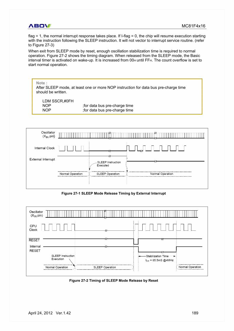
MC81F4x16
April 24, 2012 Ver.1.42 189
flag = 1, the normal interrupt response takes place. If I-flag = 0, the chip will resume execution starting with the instruction following the SLEEP instruction. It will not vector to interrupt service routine. (refer to Figure 27-3) When exit from SLEEP mode by reset, enough oscillation stabilization time is required to normal operation. Figure 27-2 shows the timing diagram. When released from the SLEEP mode, the Basic interval timer is activated on wake-up. It is increased from 00H until FFH. The count overflow is set to start normal operation.
Note : After SLEEP mode, at least one or more NOP instruction for data bus pre-charge time should be written.
LDM SSCR,#0FH NOP ;for data bus pre-charge time NOP ;for data bus pre-charge time
Figure 27-1 SLEEP Mode Release Timing by External Interrupt
Figure 27-2 Timing of SLEEP Mode Release by Reset

MC81F4x16
190 April 24, 2012 Ver.1.42
27.2 Stop Mode
In the Stop mode, the system clock and the peripheral clocks are stopped, but the unselected clock source is keep running. See the” Table 27-1 Peripheral Operation During Power Saving Mode” for more information. The states of the RAM, registers, and latches valid immediately before the system is put in the STOP state are all held. The program counter stop the address of the instruction to be executed after the instruction "STOP" which starts the STOP operating mode.
Note : The Stop mode is activated by execution of STOP instruction after setting the SSCR to “5AH”. (This register should be written by byte operation. If this register is set by bit manipulation instruction, for example "set1" or "clr1" instruction, it may be undesired operation)
In the Stop mode of operation, VDD can be reduced to minimize power consumption. Care must be taken, however, to ensure that VDD is not reduced before the Stop mode is invoked, and that VDD is restored to its normal operating level, before the Stop mode is terminated. The reset should not be activated before VDD is restored to its normal operating level, and must be held active long enough to allow the oscillator to restart and stabilize.
Note : After STOP instruction, at least two or more NOP instruction should be written. Ex)
LDM CKCTLR,#0FH ;more than 20ms LDM SSCR,#5AH STOP NOP ;for stabilization time NOP ;for stabilization time
In the STOP operation, the dissipation of the power associated with the oscillator and the internal hardware is lowered; however, the power dissipation associated with the pin interface (depending on the external circuitry and program) is not directly determined by the hardware operation of the STOP feature. This point should be little current flows when the input level is stable at the power voltage level (VDD/VSS); however, when the input level gets higher than the power voltage level (by approximately 0.3 to 0.5V), a current begins to flow. Therefore, if cutting off the output transistor at an I/O port puts the pin signal into the high-impedance state, a current flow across the ports input transistor, requiring to fix the level by pull-up or other means.

MC81F4x16
April 24, 2012 Ver.1.42 191
Release the STOP mode The source for exit from STOP mode is hardware reset, external interrupt, Timer, Watch Timer, IIC Slave, SIO or UART. Reset re-defines all the Control registers but does not change the on-chip RAM(Be careful, If the code is compiled with RAM clear option, RAM is cleared after reset by ram clear routine. It is possible to disable the RAM clear option by option menu). If I-flag = 1, the normal interrupt response takes place. If I-flag = 0, the chip will resume execution starting with the instruction following the STOP instruction. It will not vector to interrupt service routine. (refer to Figure 27-3) When exit from Stop mode by external interrupt, enough oscillation stabilization time is required to normal operation. Figure 27-4 shows the timing diagram. When released from the Stop mode, the Basic interval timer is activated on wake-up. It is increased from 00H until FFH. The count overflow is set to start normal operation. Therefore, before STOP instruction, user must be set its relevant prescaler divide ratio to have long enough time (more than 20msec). This guarantees that oscillator has started and stabilized. By reset, exit from Stop mode is shown in Figure 27-5.
Figure 27-3 STOP Releasing Flow by Interrupts

MC81F4x16
192 April 24, 2012 Ver.1.42
Figure 27-4 STOP Mode Release Timing by External Interrupt
Figure 27-5 of STOP Mode Release by Reset

MC81F4x16
April 24, 2012 Ver.1.42 193
27.3 Sleep vs Stop
Peripheral STOP in Main OSC
STOP in SUB OSC
SLEEP Mode
CPU Stop Stop
RAM Retain Retain
I/O Ports Retain Retain
Control Registers Retain Retain
Address Data Bus Retain Retain
ADC Stop Operate
Usart Stop Operate
SIO Only operated with external clock Operate
IIC Slave Operate Operate
Basic Interval Timer Stop Operate
Watchdog Timer Stop Operate
Watch Timer with System clock Stop Operate
Timer/Counter with System clock Stop Operate
Buzzer with System clock Stop Operate
Watch Timer with Sub clock Operate Stop Operate
Timer/Counter with Sub clock Operate Stop Operate
Buzzer with Sub clock Operate Stop Operate
Main Oscillator Stop Oscillation Oscillation
Sub Oscillator Oscillation Stop Oscillation
Release Source Reset, Timer(0,1,2,3) ,Watch Timer(with Sub clock)
, SIO, USART, IIC Slave ,External Interrupt
Reset, All Interrupts
Note: In the stop mode, system clock source is stopped. But unselected clock source is not stopped. For example, when main oscillator is selected as the system clock and the stop instruction is executed, main oscillator is stopped, but sub oscillator is not stopped. (assume that, both oscillator are working before stop instruction) In this case, the watch timer can be operated with sub oscillator.
Table 27-1 Peripheral Operation During Power Saving Mode
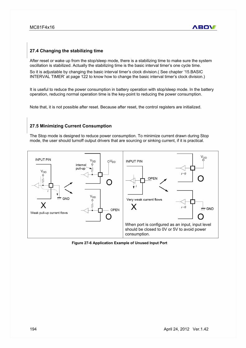
MC81F4x16
194 April 24, 2012 Ver.1.42
27.4 Changing the stabilizing time
After reset or wake up from the stop/sleep mode, there is a stabilizing time to make sure the system oscillation is stabilized. Actually the stabilizing time is the basic interval timer’s one cycle time. So it is adjustable by changing the basic interval timer’s clock division.( See chapter ‘15.BASIC INTERVAL TIMER’ at page 122 to know how to change the basic interval timer’s clock division.) It is useful to reduce the power consumption in battery operation with stop/sleep mode. In the battery operation, reducing normal operation time is the key-point to reducing the power consumption. Note that, it is not possible after reset. Because after reset, the control registers are initialized.
27.5 Minimizing Current Consumption
The Stop mode is designed to reduce power consumption. To minimize current drawn during Stop mode, the user should turnoff output drivers that are sourcing or sinking current, if it is practical.
When port is configured as an input, input level should be closed to 0V or 5V to avoid power consumption.
Figure 27-6 Application Example of Unused Input Port

MC81F4x16
April 24, 2012 Ver.1.42 195
In the left case, much current flows from port to GND.
In the left case, Tr. base current flows from port to GND. To avoid power consumption, there should be low output to the port.
Note : In the STOP operation, the power dissipation associated with the oscillator and the internal hardware is lowered; however, the power dissipation associated with the pin interface (depending on the external circuitry and program) is not directly determined by the hardware operation of the STOP feature. This point should be little current flows when the input level is stable at the power voltage level (VDD/VSS); however, when the input level becomes higher than the power voltage level (by approximately 0.3V), a current begins to flow. Therefore, if cutting off the output transistor at an I/O port puts the pin signal into the high impedance state, a current flow across the ports input transistor, requiring it to fix the level by pull-up or other means.
It should be set properly in order that current flow through port doesn't exist. First consider the port setting to input mode. Be sure that there is circuit. In input mode, the pin impedance viewing from external MCU is very high that the current doesn’t flow. But input voltage level should be VSS or VDD. Be careful that if unspecified voltage, i.e. if uncertain voltage level (not VSS or VDD) is applied to input pin, there can be little current (max. 1mA at around 2V) flow. If it is not appropriate to set as an input mode, then set to output mode considering there is no current flow. The port setting to High or Low is decided by considering its relationship with external circuit. For example, if there is external pull-up resistor then it is set to output mode, i.e. to High, and if there is external pull-down register, it is set to low.
Figure 27-7 Application Example of Unused Output Port

MC81F4x16
196 April 24, 2012 Ver.1.42
28. EMULATOR
① ②
③
⑤
④
⑥
⑦ ⑧

MC81F4x16
April 24, 2012 Ver.1.42 197
Mark Name Description
SW5.1 – SELL4x16
SW5.2 – SELL4204
Those two switch are used to select the device mode SW5.1 :On & SW5.2:On : 4432 mode SW5.1 :Off & SW5.2:On : 4x16 mode SW5.1 :On & SW5.2:Off : 4204 mode
SW5.3 - MODE It is used for developing emulator. So, user must turn it off always.
①
SW5.4 Not Connected
SW4.1 – OSCS.0
SW4.2 – OSCS.1
SW4.3 – OSCS.2
Rom Option bit 0~2 : OSC Selection bits ( On : 1, Off : 0 ) 000: External RC 001: Internal RC; 4MHz 010: Internal RC; 2MHz 011: Internal RC; 1MHz 100: Internal RC; 8MHz 101: Not available 110: Not available 111: Crystal/ceramic oscillator
SW4.4 Not Connected
SW4.5 Not Connected
SW4.6 – LVRS.0
SW4.7 – LVRS.1
Rom Option bit 5~6 : Low Voltage Reset Level Selection bit( On: 1, Off : 0 ) 00: 2.4V 10: 3.0V 01: 2.7V 11: 4.0V
②
SW4.8 – LVREN Rom Option bit 7 : Low Voltage Reset Enable bit On : (1) Disable ( RESETB ) Off : (0) Enable ( R35 )
SW3.1 – R34 On : Connect the XTAL to R34/XIN pin Off : Disconnect
SW3.2 – R33 On : Connect the XTAL to R33/XOUT pin Off : Disconnect
SW3.3 – R34 On : Connect the EXT.RC to R34/XIN pin Off : Disconnect
SW3.4 – R35 On : Connect the Reset to R35/Reset pin Off : Disconnect
SW3.5 – R00 On : Connect the Sub-Clock to R00/SXIN pin Off : Disconnect
③
SW3.6 – R01 On : Connect the Sub-Clock to R01/SXOUT pin Off : Disconnect
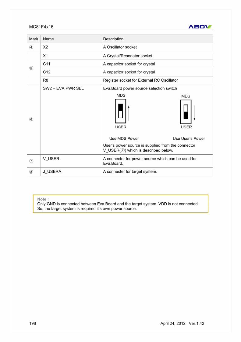
MC81F4x16
198 April 24, 2012 Ver.1.42
Mark Name Description
④ X2 A Oscillator socket
X1 A Crystal/Resonator socket
C11 A capacitor socket for crystal
C12 A capacitor socket for crystal ⑤
R8 Register socket for External RC Oscillator
⑥
SW2 – EVA PWR SEL Eva.Board power source selection switch
User’s power source is supplied from the connector V_USER(⑦) which is described below.
⑦ V_USER A connector for power source which can be used for Eva.Board.
⑧ J_USERA A connecter for target system.
Note : Only GND is connected between Eva.Board and the target system. VDD is not connected. So, the target system is required it’s own power source.

MC81F4x16
April 24, 2012 Ver.1.42 199
29. IN SYSTEM PROGRAMMING
29.1 Getting Started
The In-System Programming (ISP) is an ability to program the code into the MCU while it is installed in a complete system. USB_SIO_ISP uses both USB to communicate with PC and SIO to communicate with MCU. That is why we call it as ‘USB_SIO_ISP’. In fact there are another ISP types. So remember that all MC81F4xxx series use ‘USB_SIO_ISP’. Here is a procedure to use ISP. 1. Power off the target system. If you use the RESET/Vpp pin as an output mode, power on timing is very important. So you must read ‘Entering ISP mode at power on time’ and strictly obey the procedure. 2. Install the USB_SIO_ISP software. (It is required at only first time) 1) Download the ISP software from http://www.abov.co.kr 2) Unzip the downloaded file and connect the USB_SIO_ISP board. 3) Install the driver for USB_SIO_ISP. (There is a driver file in the zip file.) 3. Make sure the hardware condition is satisfied. And connect the ISP cable.
See ‘29.3 Hardware Conditions to Enter the ISP Mode’ page 202, 4. Run the software and select a device. All commands are enabled after select the device. 5. Power on the target system. If you use the RESET/Vpp pin as an input mode, power on timing is not that important. But make sure the power is turned-on before execute the ISP commands. 6. Execute ISP commands as you want. If you want to write a code into your MCU, it is recommendable to do following step. ‘Load File’ -> ‘Auto’( while ‘Auto Option Write’ and ‘Auto Show Option’ options are
enabled ). After finish an ISP command is executed, the MCU enters to normal operation mode automatically. So you can see the system is working right after the ISP command is finished. ( ‘Auto’ is assumed as one command’) In fact, it is possible to repeat the step-6 until the hardware condition is changed. But in case of RESET/Vpp pin is used as an output mode, do not repeat step-6. In that case, you must follow the procedure. See ‘Entering ISP mode at power on time’ for more information. After you change the ‘Rom Option’, you must do power-off and power-on to reflect the changed ‘Rom Option’, even you can repeat the step-6 and see the changed code’s operation without doing it. The MCU reads the ‘Rom option’ when only the ‘power on reset time’.

MC81F4x16
200 April 24, 2012 Ver.1.42
29.2 Basic ISP S/W Information
The Figure 29-1 is the USB_SIO_ISP software based on MS-Windows. This software supports only SIO_ISP type devices.
Function Description
Load File Load the data from the selected file storage into the memory buffer.
Save File Save the current data in your memory buffer to a disk storage by using the Intel Motorola HEX format.
Blank Check Verify whether or not a device is in an erased or unprogrammed state. Program This button enables you to place new data from the memory buffer into the target device.
Program Write the current data into the MCU.
Read Read the data in the target MCU into the buffer for examination. The checksum will be displayed on the checksum box.
Verify Assures that data in the device matches data in the memory buffer. If your device is secured, a verification error is detected.
Figure 29-1 ISP Software
MC81F4x16
April 24, 2012 Ver.1.42 201
Erase Erase the data in your target MCU before programming it.
Option Selection Set the configuration data of target MCU. The security locking is set with this button.
Option Write Progam the configuration data of target MCU. The security locking is performed with this button.
AUTO Following sequence is performed ; 1.Erase 2.Program 3.Verify 4.Option Write
Auto Option Write Enable the option writing when the ‘AUTO’ sequence is executing.
Auto Show Option Enable showing the option window when ‘AUTO’ button is pressed.
Ver. Info It shows the version information.
Log It shows/hides the log windows
Hex Edit It shows/hides ‘Hex editor’. In ‘Hex editor’ you can modify the currently loaded data.
Fill Buffer Fill the selected area with a data.
Goto Display the selected page.
Start ______ Starting address
End ______ End address
Checksum Display the check sum(Hex decimal) after reading the target device.
Option It shows currently selected option code in hexadecimal.
Device Select It is used to select a target device.
Device It shows currently selected device.
Note: MCU Configuration value is erased after erase operation. It must be configured to match with user target board. Otherwise, it is failed to enter ISP mode, or its operation is not desirable.

MC81F4x16
202 April 24, 2012 Ver.1.42
29.3 Hardware Conditions to Enter the ISP Mode
Anytime RESET/ Vpp pin goes +9V, the MCU entering an ISP mode except RESET/Vpp pin is output mode(See note1).
1. If other signals affect SIO communication in ISP mode, disconnect these pins by using a jumper or a switch.
Note: 1) Using RESET/Vpp pin as an output mode is not recommended even it is possible. Anytime RESET/Vpp pin goes +9v, the MCU entering an ISP mode except RESET/Vpp pin is output mode. If it is output mode, +9v signal is clashing with the output voltage. So if RESET/Vpp pin is used as an output mode, do not try to execute any ISP commands when MCU is in normal operation mode. It is allowable when only power on time. See ‘Entering ISP mode at power on time’ for more information. 2) There is a 10KΩ pull-down register at VPP pin in the ISP Board. That is why 75KΩ register is suggested for R/C reset circuit. So those two register makes a voltage divider circuit when ISP board is connected. So the VPP level can’t go down to low level status if the register of reset circuit value is too small. Otherwise, if the register value is too large the capacitor value also changed and the reset circuit’s characteristics also changed.
Figure 29-2 Hardware Conditions to Enter the ISP Mode
RESET/Vpp
SDATA SCLK
GND XoutVDDXin
7 5 3 1 98 6 4 2 10
0.1uF 75KΩ
VDD(+5v)
User reset circuitry
User Target Board
VD
DG
ND
SC
LKS
DA
TAVPP
USB-SIO-ISP B/D 10-pin connector
PCB Top View
MC81F4x16
April 24, 2012 Ver.1.42 203
29.4 Entering ISP mode at power on time
Basically anytime +9v signal is forced to RESET/Vpp pin, the MCU is entering into ISP mode. But it makes trouble when the RESET/Vpp pin is output mode. Because the +9v signal is clashing with the port’s output voltage. But it is possible to enter the ISP mode at the power on time even RESET/Vpp pin is used as an output mode. There is an oscillator stabilizing time when power is turn on. While in the time RESET/Vpp pin is in input mode even it is used as an output mode in operation time. A proper procedure is required to make sure that ISP board catch the oscillator stabilizing time to enter the ISP mode. See following procedure.
1. Power off the target system. 2. Configure the target system as ISP mode. 3. Attach a ISP B/D into the target system. 4. Run the ISP S/W 5. Select the target device. 6. Power on the target system. 7. Execute ISP commands as you want.
Note : Power on the target system after select the target device is essential. Because when target device is selected, ISP board is getting ready to catch the proper timing to rise the Vpp(+9v) signal.

MC81F4x16
204 April 24, 2012 Ver.1.42
29.5 USB-SIO-ISP Board
Figure 29-3 USB-SIO-ISP Board
Connect USB -mini type cable
MC81F4x16
April 24, 2012 Ver.1.42 205
30. INSTRUCTION SET
30.1 Terminology List
A Accumulator
X X - register
Y Y - register
PSW Program Status Word
#imm 8-bit Immediate data
dp Direct Page Offset Address
!abs Absolute Address
[ ] Indirect expression
Register Indirect expression
+ Register Indirect expression, after that, Register auto-increment
.bit Bit Position
A.bit Bit Position of Accumulator
dp.bit Bit Position of Direct Page Memory
M.bit Bit Position of Memory Data (000H~0FFFH)
rel Relative Addressing Data
upage U-page (0FF00H~0FFFFH) Offset Address
n Table CALL Number (0~15)
+ Addition
x
Upper Nibble Expression in Opcode when it is even number (bit7~bit5, bit4=0)
y Upper Nibble Expression in Opcode when it is odd number (bit7~bit5, bit4=1)
− Subtraction
× Multiplication
⁄ Division
( ) Contents Expression
∧ AND
∨ OR
⊕ Exclusive OR
~ NOT
← Assignment / Transfer / Shift Left
→ Shift Right
Bit Position
1
Bit Position
0
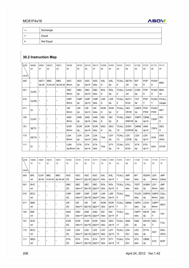
MC81F4x16
206 April 24, 2012 Ver.1.42
↔ Exchange
= Equal
≠ Not Equal
30.2 Instruction Map
LOW
HIGH
00000
00
00001
01
00010
02
00011
03
00100
04
00101
05
00110
06
00111
07
01000
08
01001
09
01010
0A
01011
0B
01100
0C
01101
0D
01110
0E
01111
0F
000 -
SET1
dp.bit
BBS
A.bit,rel
BBS
dp.bit,rel
ADC
#imm
ADC
dp
ADC
dp+X
ADC
!abs
ASL
A
ASL
dp
TCALL
0
SETA1
.bit
BIT
dp
POP
A
PUSH
A BRK
001 CLRC ″ ″ ″
SBC
#imm
SBC
dp
SBC
dp+X
SBC
!abs
ROL
A
ROL
dp
TCALL
2
CLRA1
.bit
COM
dp
POP
X
PUSH
X
BRA
rel
010 CLRG ″ ″ ″
CMP
#imm
CMP
dp
CMP
dp+X
CMP
!abs
LSR
A
LSR
dp
TCALL
4
NOT1
M.bit
TST
dp
POP
Y
PUSH
Y
PCALL
Upage
011 DI ″ ″ ″
OR
#imm
OR
dp
OR
dp+X
OR
!abs
ROR
A
ROR
dp
TCALL
6
OR1
OR1B
CMPX
dp
POP
PSW
PUSH
PSWRET
100 CLRV ″ ″ ″
AND
#imm
AND
dp
AND
dp+X
AND
!abs
INC
A
INC
dp
TCALL
8
AND1
AND1B
CMPY
dp
CBNE
dp+X TXSP
INC
X
101 SETC ″ ″ ″
EOR
#imm
EOR
dp
EOR
dp+X
EOR
!abs
DEC
A
DEC
dp
TCALL
10
EOR1
EOR1B
DBNE
dp
XMA
dp+X TSPX
DEC
X
110 SETG ″ ″ ″
LDA
#imm
LDA
dp
LDA
dp+X
LDA
!abs TXA
LDY
dp
TCALL
12
LDC
LDCB
LDX
dp
LDX
dp+Y XCN
DAS
(N/A)
111 EI ″ ″ ″
LDM
dp,#imm
STA
dp
STA
dp+X
STA
!abs TAX
STY
dp
TCALL
14
STC
M.bit
STX
dp
STX
dp+Y XAX STOP
LOW
HIGH
10000
10
10001
11
10010
12
10011
13
10100
14
10101
15
10110
16
10111
17
11000
18
11001
19
11010
1A
11011
1B
11100
1C
11101
1D
11110
1E
11111
1F
000 BPL
rel
CLR1
dp.bit
BBC
A.bit,rel
BBC
dp.bit,rel
ADC
X
ADC
!abs+Y
ADC
[dp+X]
ADC
[dp]+Y
ASL
!abs
ASL
dp+X
TCALL
1
JMP
!abs
BIT
!abs
ADDW
dp
LDX
#imm
JMP
[!abs]
001 BVC
rel ″ ″ ″
SBC
X
SBC
!abs+Y
SBC
[dp+X]
SBC
[dp]+Y
ROL
!abs
ROL
dp+X
TCALL
3
CALL
!abs
TEST
!abs
SUBW
dp
LDY
#imm
JMP
[dp]
010 BCC
rel ″ ″ ″
CMP
X
CMP
!abs+Y
CMP
[dp+X]
CMP
[dp]+Y
LSR
!abs
LSR
dp+X
TCALL
5 MUL
TCLR1
!abs
CMPW
dp
CMPX
#imm
CALL
[dp]
011 BNE
rel ″ ″ ″
OR
X
OR
!abs+Y
OR
[dp+X]
OR
[dp]+Y
ROR
!abs
ROR
dp+X
TCALL
7
DBNE
Y
CMPX
!abs
LDYA
dp
CMPY
#immRETI
100 BMI
rel ″ ″ ″
AND
X
AND
!abs+Y
AND
[dp+X]
AND
[dp]+Y
INC
!abs
INC
dp+X
TCALL
9 DIV
CMPY
!abs
INCW
dp
INC
Y TAY
101 BVS
rel ″ ″ ″
EOR
X
EOR
!abs+Y
EOR
[dp+X]
EOR
[dp]+Y
DEC
!abs
DEC
dp+X
TCALL
11
XMA
X
XMA
dp
DECW
dp
DEC
Y TYA
110 BCS
rel ″ ″ ″
LDA
X
LDA
!abs+Y
LDA
[dp+X]
LDA
[dp]+Y
LDY
!abs
LDY
dp+X
TCALL
13
LDA
X+
LDX
!abs
STYA
dp XAY
DAA
(N/A)
111 BEQ
rel ″ ″ ″
STA
X
STA
!abs+Y
STA
[dp+X]
STA
[dp]+Y
STY
!abs
STY
dp+X
TCALL
15
STA
X+
STX
!abs
CBNE
dp XYX NOP

MC81F4x16
April 24, 2012 Ver.1.42 207
30.3 Instruction Set
Arithmetic / Logic
NO. MNEMONIC OP CODE
BYTE NO
CYCLE NO OPERATION
FLAG NVGBHIZC
1 ADC #imm 04 2 2
2 ADC dp 05 2 3
3 ADC dp + X 06 2 4
4 ADC !abs 07 3 4
5 ADC !abs + Y 15 3 5
6 ADC [ dp + X ] 16 2 6
7 ADC [ dp ] + Y 17 2 6
8 ADC X 14 1 3
Add with carry.
A ← ( A ) + ( M ) + C NV--H-ZC
9 AND #imm 84 2 2
10 AND dp 85 2 3
11 AND dp + X 86 2 4
12 AND !abs 87 3 4
13 AND !abs + Y 95 3 5
14 AND [ dp + X ] 96 2 6
15 AND [ dp ] + Y 97 2 6
16 AND X 94 1 3
Logical AND
A ← ( A ) ∧ ( M ) N-----Z-
17 ASL A 08 1 2
18 ASL dp 09 2 4
19 ASL dp + X 19 2 5
20 ASL !abs 18 3 5
Arithmetic shift left
N-----ZC
21 CMP #imm 44 2 2
22 CMP dp 45 2 3
23 CMP dp + X 46 2 4
24 CMP !abs 47 3 4
25 CMP !abs + Y 55 3 5
26 CMP [ dp + X ] 56 2 6
Compare accumulator contents with memory contents ( A ) - ( M )
N-----ZC
“0” C 7 6 5 4 3 2 1 0
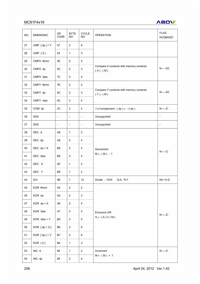
MC81F4x16
208 April 24, 2012 Ver.1.42
NO. MNEMONIC OP CODE
BYTE NO
CYCLE NO OPERATION
FLAG NVGBHIZC
27 CMP [ dp ] + Y 57 2 6
28 CMP X 54 1 3
29 CMPX #imm 5E 2 2
30 CMPX dp 6C 2 3
31 CMPX !abs 7C 3 4
Compare X contents with memory contents ( X ) - ( M )
N-----ZC
32 CMPY #imm 7E 2 2
33 CMPY dp 8C 2 3
34 CMPY !abs 9C 3 4
Compare Y contents with memory contents ( Y ) - ( M )
N-----ZC
35 COM dp 2C 2 4 1’s Complement : ( dp ) ← ~( dp ) N-----Z-
36 DAA - - - Unsupported -
37 DAS - - - Unsupported -
38 DEC A A8 1 2
39 DEC dp A9 2 4
40 DEC dp + X B9 2 5
41 DEC !abs B8 3 5
42 DEC X AF 1 2
43 DEC Y BE 1 2
Decrement
M ← ( M ) - 1 N-----Z-
44 DIV 9B 1 12 Divide : YA/X Q:A, R:Y NV--H-Z-
45 EOR #imm A4 2 2
46 EOR dp A5 2 3
47 EOR dp + X A6 2 4
48 EOR !abs A7 3 4
49 EOR !abs + Y B5 3 5
50 EOR [ dp + X ] B6 2 6
51 EOR [ dp ] + Y B7 2 6
52 EOR X B4 1 3
Exclusive OR
A ← ( A ) ⊕ ( M ) N-----Z-
53 INC A 88 1 2
54 INC dp 89 2 4
Increment
M ← ( M ) + 1
N-----Z-

MC81F4x16
April 24, 2012 Ver.1.42 209
NO. MNEMONIC OP CODE
BYTE NO
CYCLE NO OPERATION
FLAG NVGBHIZC
55 INC dp + X 99 2 5
56 INC !abs 98 3 5
57 INC X 8F 1 2
58 INC Y 9E 1 2
59 LSR A 48 1 2
60 LSR dp 49 2 4
61 LSR dp + X 59 2 5
62 LSR !abs 58 3 5
Arithmetic shift left
N-----ZC
63 MUL 5B 1 9 Multiply : YA ← Y × A N-----Z-
64 OR #imm 64 2 2
65 OR dp 65 2 3
66 OR dp + X 66 2 4
67 OR !abs 67 3 4
68 OR !abs + Y 75 3 5
69 OR [ dp + X ] 76 2 6
70 OR [ dp ] + Y 77 2 6
71 OR X 74 1 3
Logical OR
A ← ( A ) ∨ ( M ) N-----Z-
72 ROL A 28 1 2
73 ROL dp 29 2 4
74 ROL dp + X 39 2 5
75 ROL !abs 38 3 5
Rotate left through carry
N-----ZC
76 ROR A 68 1 2
77 ROR dp 69 2 4
78 ROR dp + X 79 2 5
79 ROR !abs 78 3 5
Rotate right through carry
N-----ZC
80 SBC #imm 24 2 2
81 SBC dp 25 2 3
82 SBC dp + X 26 2 4
Subtract with carry
A ← ( A ) - ( M ) - ~( C )
NV--HZC
7 6 5 4 3 2 1 0 C
C 7 6 5 4 3 2 1 0
“0”7 6 5 4 3 2 1 0 C

MC81F4x16
210 April 24, 2012 Ver.1.42
NO. MNEMONIC OP CODE
BYTE NO
CYCLE NO OPERATION
FLAG NVGBHIZC
83 SBC !abs 27 3 4
84 SBC !abs + Y 35 3 5
85 SBC [ dp + X ] 36 2 6
86 SBC [ dp ] + Y 37 2 6
87 SBC X 34 1 3
88 TST dlp 4C 2 3 Test memory contents for negative or zero ( dp ) – 00H
N-----Z-
89 XCN CE 1 5 Exchange nibbles within the accumulator
A7~A4 ↔ A3~A0 N-----Z-

MC81F4x16
April 24, 2012 Ver.1.42 211
Register / Memory Operation
NO. MNEMONIC OP CODE
BYTE NO
CYCLE NO OPERATION
FLAG NVGBHIZC
1 LDA #imm C4 2 2
2 LDA dp C5 2 3
3 LDA dp + X C6 2 4
4 LDA !abs C7 3 4
5 LDA !abs + Y D5 3 5
6 LDA [ dp + X ] D6 2 6
7 LDA [ dp ] + Y D7 2 6
8 LDA X D4 1 3
Load accumulator
A ← ( M )
9 LDA X + DB 1 4 X-register auto-increment : A ← ( M ), X ← X + 1
N-----Z-
10 LDM dp, #imm E4 3 5 Load memory with immediate data :
( M ) ← imm --------
11 LDX #imm 1E 2 2
12 LDX dp CC 2 3
13 LDX dp + Y CD 2 4
14 LDX !abs DC 3 4
Load X-register
X ← ( M ) N-----Z-
15 LDY #imm 3E 2 2
16 LDY dp C9 2 3
17 LDY dp + Y D9 2 4
18 LDY !abs D8 3 4
Load Y-register
Y ← ( M ) N-----Z-
19 STA dp E5 2 4
20 STA dp + X E6 2 5
21 STA !abs E7 3 5
22 STA !abs + Y F5 3 6
23 STA [ dp + X ] F6 2 7
24 STA [ dp ] + Y F7 2 7
25 STA X F4 1 4
Store accumulator contents in memory
( M ) ← A
--------
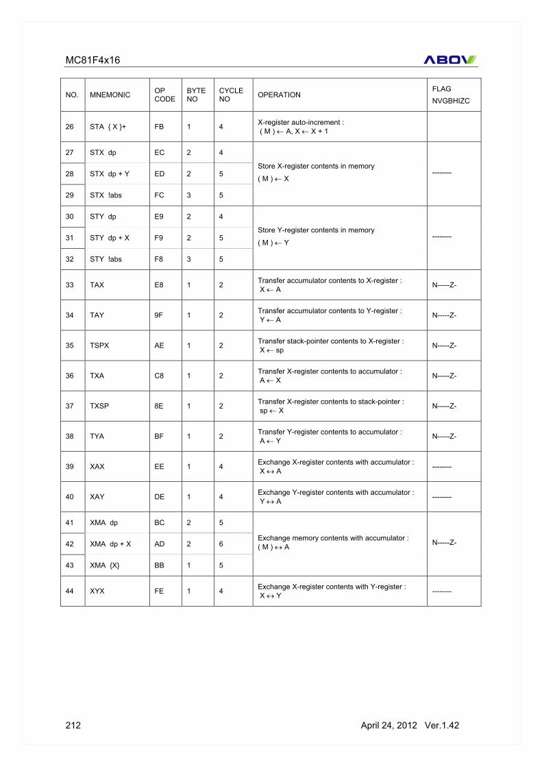
MC81F4x16
212 April 24, 2012 Ver.1.42
NO. MNEMONIC OP CODE
BYTE NO
CYCLE NO OPERATION
FLAG NVGBHIZC
26 STA X + FB 1 4 X-register auto-increment : ( M ) ← A, X ← X + 1
27 STX dp EC 2 4
28 STX dp + Y ED 2 5
29 STX !abs FC 3 5
Store X-register contents in memory
( M ) ← X --------
30 STY dp E9 2 4
31 STY dp + X F9 2 5
32 STY !abs F8 3 5
Store Y-register contents in memory
( M ) ← Y --------
33 TAX E8 1 2 Transfer accumulator contents to X-register : X ← A N-----Z-
34 TAY 9F 1 2 Transfer accumulator contents to Y-register : Y ← A N-----Z-
35 TSPX AE 1 2 Transfer stack-pointer contents to X-register : X ← sp N-----Z-
36 TXA C8 1 2 Transfer X-register contents to accumulator : A ← X N-----Z-
37 TXSP 8E 1 2 Transfer X-register contents to stack-pointer : sp ← X N-----Z-
38 TYA BF 1 2 Transfer Y-register contents to accumulator : A ← Y N-----Z-
39 XAX EE 1 4 Exchange X-register contents with accumulator : X ↔ A --------
40 XAY DE 1 4 Exchange Y-register contents with accumulator : Y ↔ A --------
41 XMA dp BC 2 5
42 XMA dp + X AD 2 6
43 XMA X BB 1 5
Exchange memory contents with accumulator : ( M ) ↔ A N-----Z-
44 XYX FE 1 4 Exchange X-register contents with Y-register : X ↔ Y --------
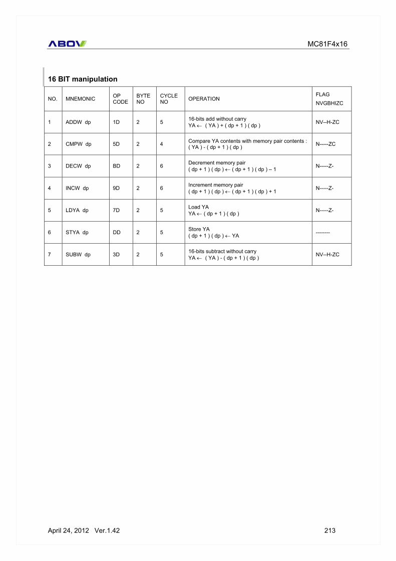
MC81F4x16
April 24, 2012 Ver.1.42 213
16 BIT manipulation
NO. MNEMONIC OP CODE
BYTE NO
CYCLE NO OPERATION
FLAG NVGBHIZC
1 ADDW dp 1D 2 5 16-bits add without carry YA ← ( YA ) + ( dp + 1 ) ( dp ) NV--H-ZC
2 CMPW dp 5D 2 4 Compare YA contents with memory pair contents : ( YA ) - ( dp + 1 ) ( dp ) N-----ZC
3 DECW dp BD 2 6 Decrement memory pair ( dp + 1 ) ( dp ) ← ( dp + 1 ) ( dp ) – 1 N-----Z-
4 INCW dp 9D 2 6 Increment memory pair ( dp + 1 ) ( dp ) ← ( dp + 1 ) ( dp ) + 1 N-----Z-
5 LDYA dp 7D 2 5 Load YA YA ← ( dp + 1 ) ( dp ) N-----Z-
6 STYA dp DD 2 5 Store YA ( dp + 1 ) ( dp ) ← YA --------
7 SUBW dp 3D 2 5 16-bits subtract without carry YA ← ( YA ) - ( dp + 1 ) ( dp ) NV--H-ZC

MC81F4x16
214 April 24, 2012 Ver.1.42
BIT manipulation
NO. MNEMONIC OP CODE
BYTE NO
CYCLE NO OPERATION
FLAG NVGBHIZC
1 AND1 M.bit 8B 3 4 Bit AND C-flag : C ← ( C ) ∧ ( M.bit ) -------C
2 AND1B M.bit 8B 3 4 Bit AND C-flag and NOT : C ← ( C ) ∧ ~( M.bit ) -------C
3 BIT dp 0C 2 4
4 BIT !abs 1C 3 5
Bit test A with memory : Z ← ( A ) ∧ ( M ), N ← ( M7 ), V ← ( M6 ) MM----Z-
5 CLR1 dp.bit y1 2 4 Clear bit : ( M.bit ) ← “0” --------
6 CLRA1 A.bit 2B 2 2 Clear A bit : ( A.bit ) ← “0” --------
7 CLRC 20 1 2 Clear C-flag : C ← “0” -------0
8 CLRG 40 1 2 Clear G-flag : G ← “0” --0-----
9 CLRV 80 1 2 Clear V-flag : V ← “0” -0--0---
10 EOR1 M.bit AB 3 5 Bit exclusive-OR C-flag : C ← ( C ) ⊕ ( M.bit ) -------C
11 EOR1B M.bit AB 3 5 Bit exclusive-OR C-flag and NOT : C ← ( C ) ⊕ ~( M.bit ) -------C
12 LDC M.bit CB 3 4 Load C-flag : C ← ( M.bit ) -------C
13 LDCB M.bit CB 3 4 Load C-flag with NOT : C ← ~( M.bit ) -------C
14 NOT1 M.bit 4B 3 5 Bit complement : ( M.bit ) ← ~( M.bit ) --------
15 OR1 M.bit 6B 3 5 Bit OR C-flag : C ← C ∨ ( M.bit ) -------C
16 OR1B M.bit 6B 3 5 Bit OR C-flag and NOT : C ← C ∨ ~ ( M.bit ) -------C
17 SET1 dp.bit x1 2 4 Set bit : ( M.bit ) ← “1” --------
18 SETA1 A.bit 0B 2 2 Set A bit : ( A.bit ) ← “1” --------
19 SETC A0 1 2 Set C-flag : C ← “1” -------1
20 SETG C0 1 2 Set G-flag : G ← “1” --1-----
21 STC M.bit EB 3 6 Store C-flag : ( M.bit ) ← C --------
22 TCLR1 !abs 5C 3 6 Test and clear bits with A : A – ( M ), ( M ) ← ( M ) ∧ ~( A ) N-----Z-
23 TSET1 !abs 3C 3 6 Test and set bits with A : A – ( M ), ( M ) ← ( M ) ∨ ( A ) N-----Z-

MC81F4x16
April 24, 2012 Ver.1.42 215
Branch / Jump
NO. MNEMONIC OP CODE
BYTE NO
CYCLE NO OPERATION
FLAG NVGBHIZC
1 BBC A.bit, rel y2 2 4/6
2 BBC dp.bit, rel y3 3 5/7
Branch if bit clear : If ( bit ) = 0, then pc ← ( pc ) + rel --------
3 BBS A.bit, rel x2 2 4/6
4 BBS dp.bit, rel x3 3 5/7
Branch if bit set : If ( bit ) = 1, then pc ← ( pc ) + rel --------
5 BCC rel 50 2 2/4 Branch if carry bit clear : If ( C ) = 0, then pc ← ( pc ) + rel --------
6 BCS rel D0 2 2/4 Branch if carry bit set : If ( C ) = 1, then pc ← ( pc ) + rel --------
7 BEQ rel F0 2 2/4 Branch if equal : If ( Z ) = 1, then pc ← ( pc ) + rel --------
8 BMI rel 90 2 2/4 Branch if minus : If ( N ) = 1, then pc ← ( pc ) + rel --------
9 BNE rel 70 2 2/4 Branch if not equal : If ( Z ) = 0, then pc ← ( pc ) + rel --------
10 BPL rel 10 2 2/4 Branch if plus : If ( N ) = 0, then pc ← ( pc ) + rel --------
11 BRA rel 2F 2 4 Branch always : pc ← ( pc ) + rel --------
12 BVC rel 30 2 2/4 Branch if overflow bit clear : If ( V ) = 0, then pc ← ( pc ) + rel --------
13 BVS rel B0 2 2/4 Branch if overflow bit set : If ( V ) = 1, then pc ← ( pc ) + rel --------
14 CALL !abs 3B 3 8
15 CALL [dp] 5F 2 8
Subroutine call M( sp ) ← ( pcH ), sp ← sp – 1, M( sp ) ← ( pcL ), sp ← sp – 1,
If !abs, pc ← abs ; if [dp], pcL ← ( dp ), pcH ← ( dp + 1 )
--------
16 CBNE dp, rel FD 3 5/7
17 CBNE dp+X, rel 8D 3 6/8
Compare and branch if not equal : if ( A ) ≠ ( M ), then pc ← ( pc ) + rel --------
18 DBNE dp, rel AC 3 5/7
19 DBNE Y, rel 7B 2 4/6
Decrement and branch if not equal : if ( M ) ≠ 0, then pc ← ( pc ) + rel --------
20 JMP !abs 1B 3 3
21 JMP [!abs] 1F 3 5
22 JMP [dp] 3F 2 4
Unconditional jump : pc ← jump address --------
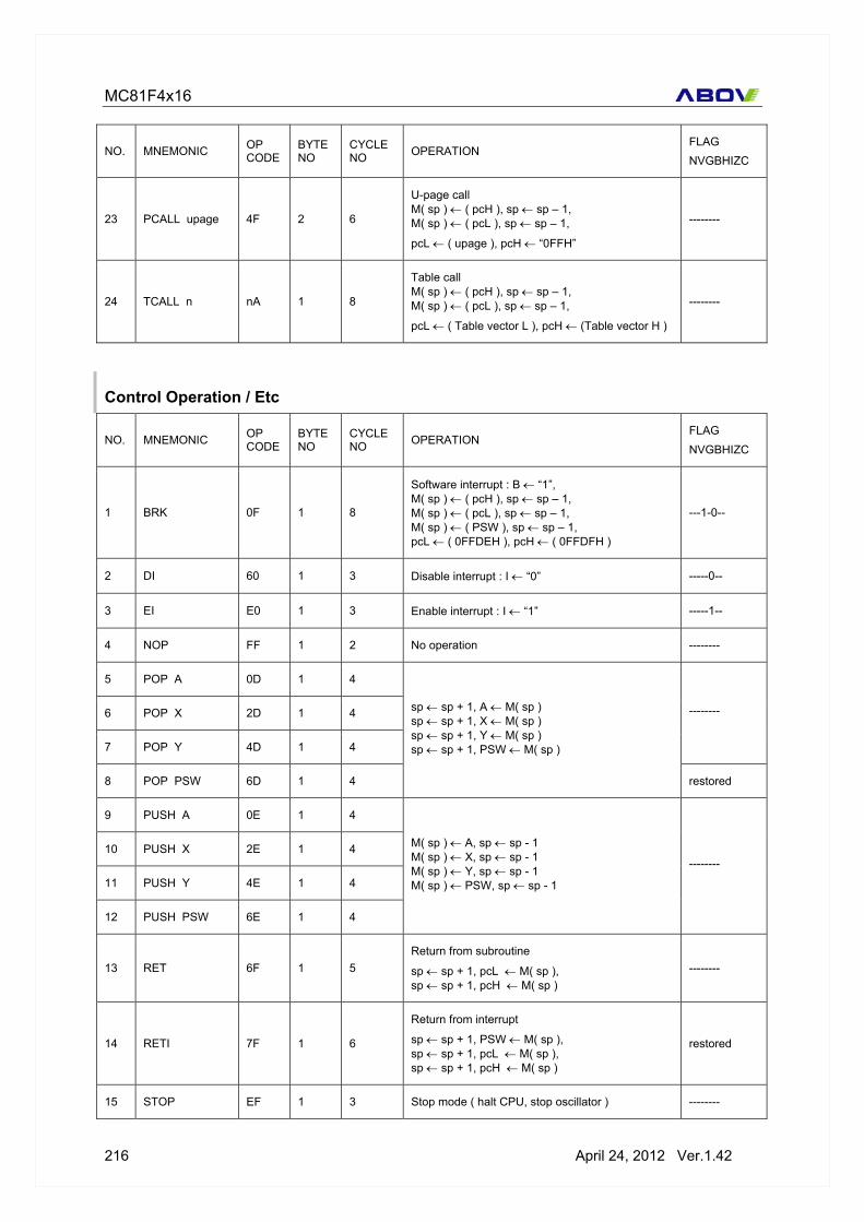
MC81F4x16
216 April 24, 2012 Ver.1.42
NO. MNEMONIC OP CODE
BYTE NO
CYCLE NO OPERATION
FLAG NVGBHIZC
23 PCALL upage 4F 2 6
U-page call M( sp ) ← ( pcH ), sp ← sp – 1, M( sp ) ← ( pcL ), sp ← sp – 1,
pcL ← ( upage ), pcH ← “0FFH”
--------
24 TCALL n nA 1 8
Table call M( sp ) ← ( pcH ), sp ← sp – 1, M( sp ) ← ( pcL ), sp ← sp – 1,
pcL ← ( Table vector L ), pcH ← (Table vector H )
--------
Control Operation / Etc
NO. MNEMONIC OP CODE
BYTE NO
CYCLE NO OPERATION
FLAG NVGBHIZC
1 BRK 0F 1 8
Software interrupt : B ← “1”, M( sp ) ← ( pcH ), sp ← sp – 1, M( sp ) ← ( pcL ), sp ← sp – 1, M( sp ) ← ( PSW ), sp ← sp – 1, pcL ← ( 0FFDEH ), pcH ← ( 0FFDFH )
---1-0--
2 DI 60 1 3 Disable interrupt : I ← “0” -----0--
3 EI E0 1 3 Enable interrupt : I ← “1” -----1--
4 NOP FF 1 2 No operation --------
5 POP A 0D 1 4
6 POP X 2D 1 4
7 POP Y 4D 1 4
--------
8 POP PSW 6D 1 4
sp ← sp + 1, A ← M( sp ) sp ← sp + 1, X ← M( sp ) sp ← sp + 1, Y ← M( sp ) sp ← sp + 1, PSW ← M( sp )
restored
9 PUSH A 0E 1 4
10 PUSH X 2E 1 4
11 PUSH Y 4E 1 4
12 PUSH PSW 6E 1 4
M( sp ) ← A, sp ← sp - 1 M( sp ) ← X, sp ← sp - 1 M( sp ) ← Y, sp ← sp - 1 M( sp ) ← PSW, sp ← sp - 1
--------
13 RET 6F 1 5 Return from subroutine
sp ← sp + 1, pcL ← M( sp ), sp ← sp + 1, pcH ← M( sp )
--------
14 RETI 7F 1 6
Return from interrupt
sp ← sp + 1, PSW ← M( sp ), sp ← sp + 1, pcL ← M( sp ), sp ← sp + 1, pcH ← M( sp )
restored
15 STOP EF 1 3 Stop mode ( halt CPU, stop oscillator ) --------

MC81F4x16
April 24, 2012 Ver.1.42 217