Mask Fabrication For Nanoimprint...
54
Canon Nanotechnologies, Inc. Mask Fabrication For Nanoimprint Lithography * [email protected] Doug Resnick Canon Nanotechnologies 1807C W. Braker Lane Austin, TX 78758
Transcript of Mask Fabrication For Nanoimprint...

Canon Nanotechnologies, Inc.
Mask Fabrication For Nanoimprint Lithography
Doug ResnickCanon Nanotechnologies
1807C W. Braker LaneAustin, TX 78758
Canon Nanotechnologies, Inc.
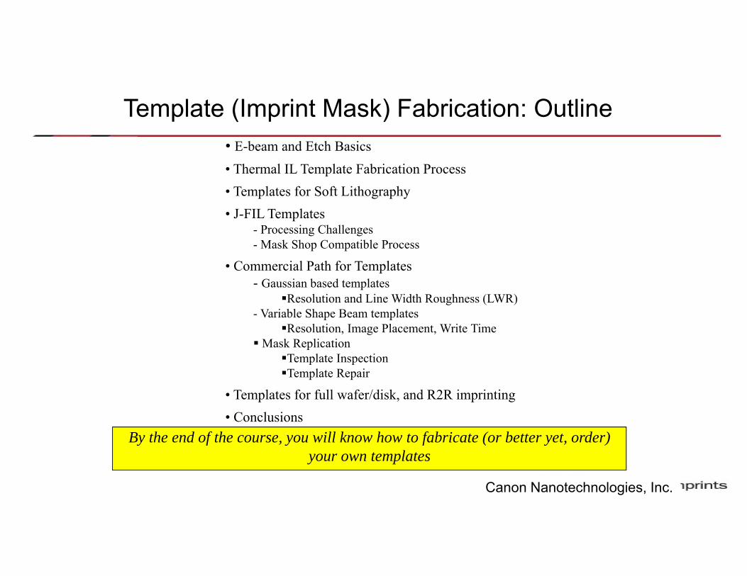
Template (Imprint Mask) Fabrication: Outline• E-beam and Etch Basics• Thermal IL Template Fabrication Process• Templates for Soft Lithography• J-FIL Templates
- Processing Challenges- Mask Shop Compatible Process
• Commercial Path for Templates- Gaussian based templates
Resolution and Line Width Roughness (LWR)- Variable Shape Beam templates
Resolution, Image Placement, Write TimeMask Replication
Template InspectionTemplate Repair
• Templates for full wafer/disk, and R2R imprinting• Conclusions
By the end of the course, you will know how to fabricate (or better yet, order)your own templates

Canon Nanotechnologies, Inc.
First, A Brief History Lesson
EUVL: Started late 1980’sEPL: Started ~ 1990MBDW: Started in the 1980’s193Immersion: Started ~2001
GutenbergPress
Imprint Lithography1041 Movable clay type invented in China.1436 Gutenberg commenced work on his press.1440 Gutenberg completed his press which used metal moving type.1455 Gutenberg completed work on his 42 Line Bible.1455 Gutenberg was effectively bankrupt.1456 Mazarw Bible printed in Mainz.1462 The attack on Mainz by soldiers of the Archbishop of Nassau,
caused printers to flee and spread their skills around Europe.1477 The first book to be printed in England (by Caxton) 1499 Printing established in more than 250 cities in Europe.

Canon Nanotechnologies, Inc.
Photomask
Fused Silica
Chromium (60 – 100nm)
• For a photomask, light is projected through the mask, through a lens (with 4x reduction optics) and an aerial image is projected into a photoresist on a silicon wafer
• For an imprint mask (or template), the final resist image depends almost entirely on the relief feature on the template
Mask Basics
6.35mm
6”

Canon Nanotechnologies, Inc.
Template FabricationFabrication of a template generally requires:- Patterning of a resist (Electron beam writing system)- Pattern transfer of the pattern into an underlying material (RIE)
E-beam Systems
Gaussian-Beam tool Shaped-Beam Tool

Canon Nanotechnologies, Inc.
Electron Beam Writing Strategies
Gaussian Beam
Electron Gun
Pros and Cons•Small spot size•Dreadfully slow•Example: Vistec VB300
Shaped BeamAperture
Pros and Cons•Much faster•Resolution limited by blur•Example: NuFlare EBM 7000

Canon Nanotechnologies, Inc.
-forward scattering coeff.-backscattering coeff.-ratio of backscattering to forward
2
2
22
2
2 expexp1)1(
1)(
rrrM
Electron Scattering Basics(Subtitle: Why electron beam lithographers are unhappy people)
Proximity Correction
Uncorrected Proximity Corrected

Canon Nanotechnologies, Inc.
Etch Basics: Sputtering
Ion Energy (eV) Reaction<3 Physical absorption4 -10 Surface sputtering10 - 5000 Sputtering
10,000 - 20,000 Implantation
• Sputtering has an angular dependence (faceting).
• Sputtering reduces the need for product volatility.
• Sputtering provides directional anisotropy.
• Inert gases provide good yields and avoid contamination.
• Redeposition is an issue.
• Aspect ratio is limited.
*After Berkeley Labs
Canon Nanotechnologies, Inc.
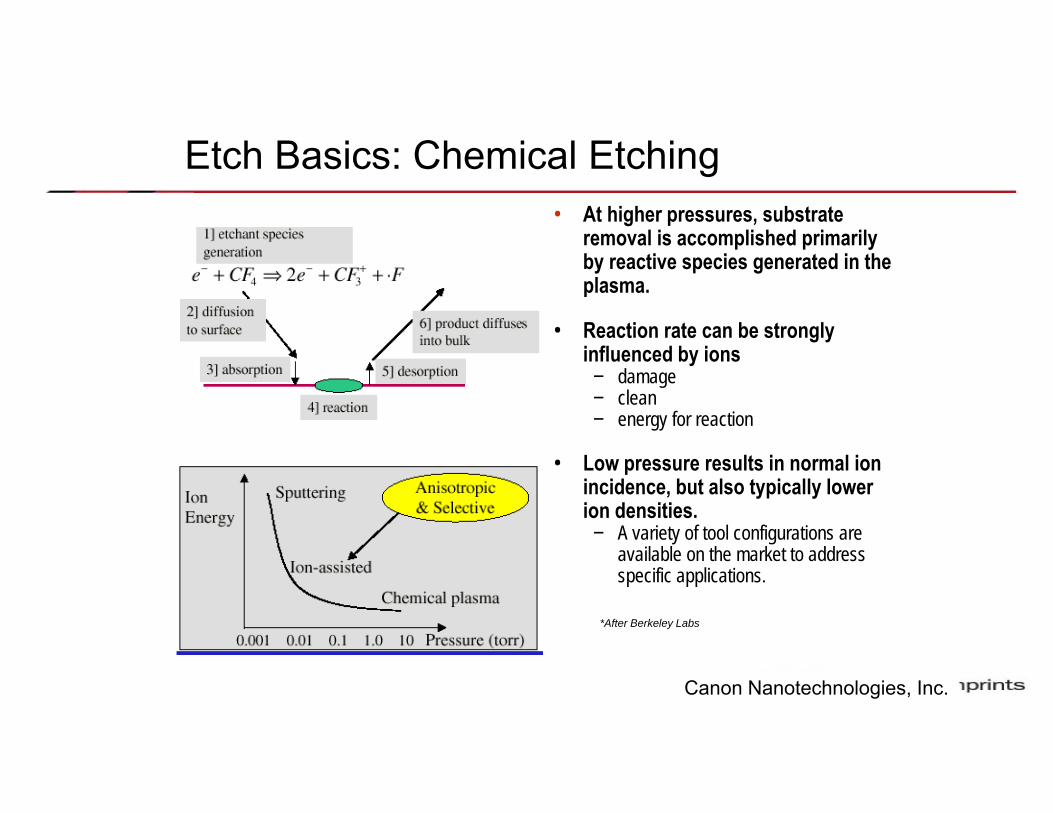
Etch Basics: Chemical Etching• At higher pressures, substrate
removal is accomplished primarily by reactive species generated in the plasma.
• Reaction rate can be strongly influenced by ions − damage − clean − energy for reaction
• Low pressure results in normal ion incidence, but also typically lower ion densities.− A variety of tool configurations are
available on the market to address specific applications.
*After Berkeley Labs

Canon Nanotechnologies, Inc.
Substrate
Template
Silicon thermoplasticThermoset
Thermal IL Process
Thermal IL Template FabricationThe most common IL template
is simply a patterned silicon wafer
silicon
E-beam pattern resist
Etch silicon
Strip Resist
Silicon can be etched withSF6, CF4, Cl2, HBr, etc…
S. Chou, Princeton

Canon Nanotechnologies, Inc.
38nm 32nm
57nm 49nm
56nm 55nm
64nm 68nm
Resist
SiliconHBr etch
Silicon Etch
• Cl2 and HBr chemistries tend to etch silicon more anistropically
• SF6 and CF4/02 tend to undercut the feature (end product is SiF4)
• Resist alone is not always a sufficient etch mask. Oxides, nitrides, and chrome are often used as hard masks
Canon Nanotechnologies, Inc.
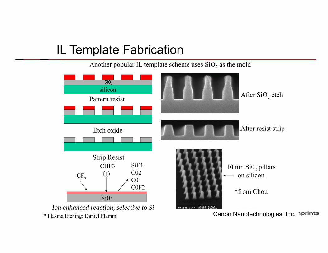
IL Template FabricationAnother popular IL template scheme uses SiO2 as the mold
After SiO2 etch
After resist strip
siliconPattern resist
Etch oxide
Strip Resist
Si02
CHF3+CFx
SiF4C02C0C0F2
* Plasma Etching: Daniel FlammIon enhanced reaction, selective to Si
10 nm Si02 pillarson silicon
*from Chou
SiO2

Canon Nanotechnologies, Inc.
Soft Lithography TemplatesSoft LithographyWhitesides, Harvard
1. PDMS template with thiol
2. Imprint stamp
3. Transfer molecules
4. Pattern Transfer
Polydimethylsiloxane (PDMS)
Elastomeric material: polymer chain of siliconcontaining oils
Example: Sylgard 184: Dow Corning
Tensile strength: 7.1 MPaElongation at break: 140 %Tear strength: 2.6 kN/m
CH3 – Si – O – Si – O – Si – CH3
CH3CH3 CH3
CH3 CH3 CH3n

Canon Nanotechnologies, Inc.
PDMS Fabrication Process
Master
Liquid Precursor to PDMS
Master Features
PDMS Stamp
Microfluidic device FET
Canon Nanotechnologies, Inc.
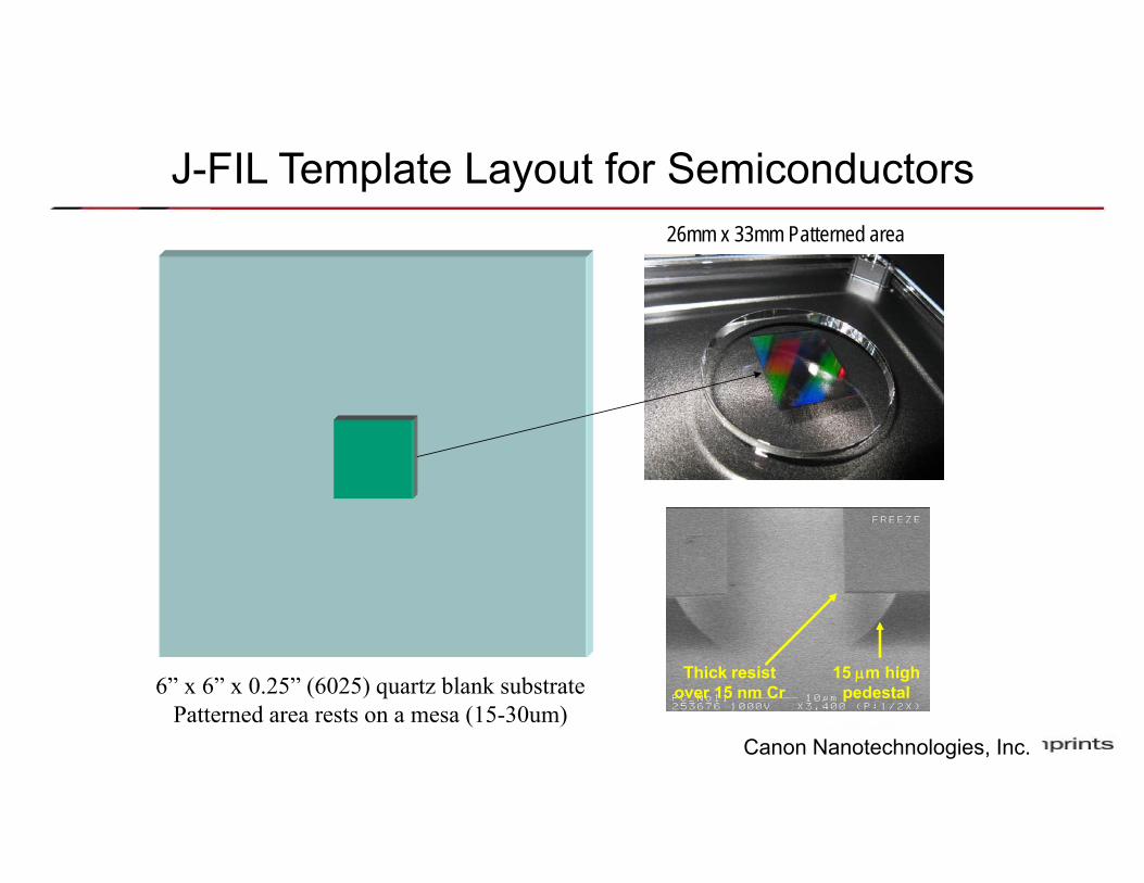
J-FIL Template Layout for Semiconductors
6” x 6” x 0.25” (6025) quartz blank substratePatterned area rests on a mesa (15-30um)
26mm x 33mm Patterned area
15 m high pedestal
Thick resist over 15 nm Cr

Canon Nanotechnologies, Inc.
UV
Transfer LayerEtch BarrierRelease Layer
Base Layer
J-FIL Template Attributes
Imprint and Expose
Etch Base layer and transfer layer
J-FIL Template
Template Attributes:
• Transparent to UV light• Compatible with a release layer• Compatible with alignment schemes• Mechanically durable• Chemically durable (cleaning)• Manufacturable
Good CD controlGood Image PlacementLow DefectivityInspectable: UV, DUV, e-beamRepairable
Canon Nanotechnologies, Inc.
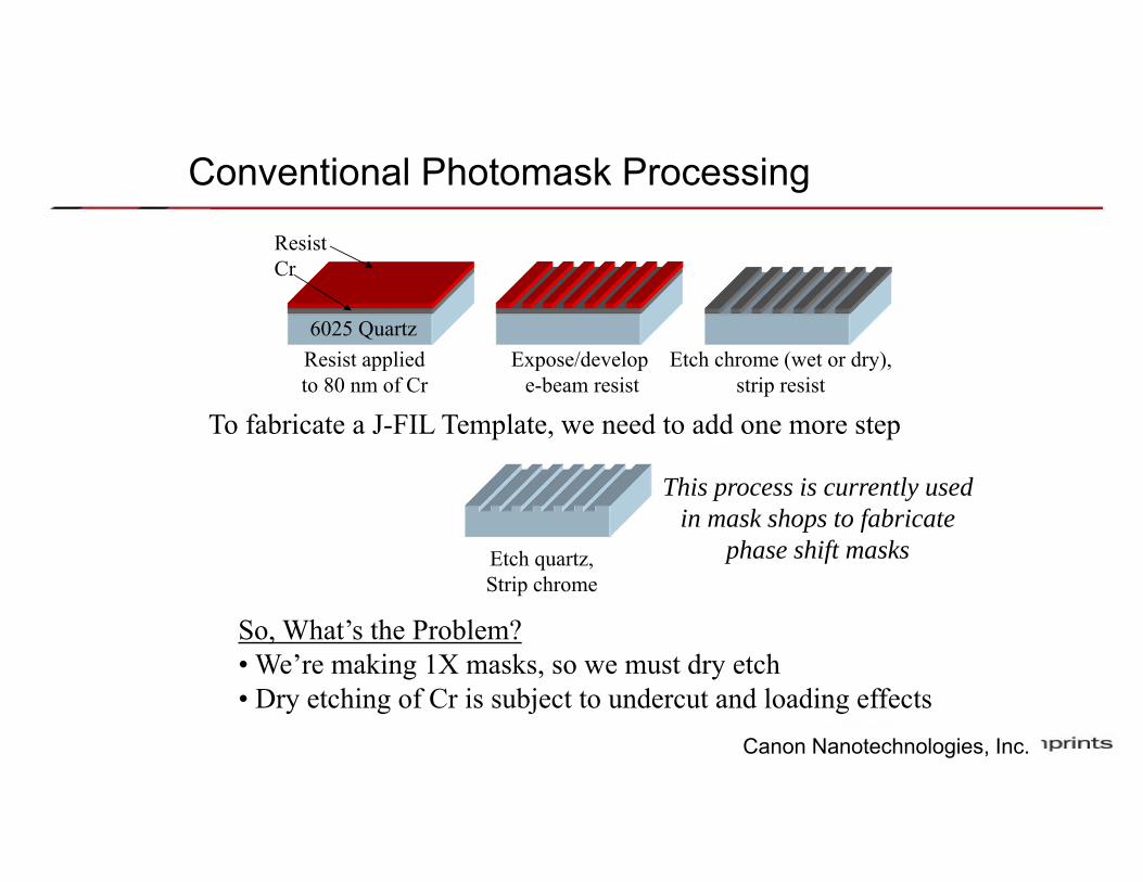
Resist appliedto 80 nm of Cr
Expose/develop e-beam resist
Etch chrome (wet or dry),strip resist
6025 Quartz
ResistCr
Conventional Photomask Processing
Etch quartz,Strip chrome
To fabricate a J-FIL Template, we need to add one more step
This process is currently usedin mask shops to fabricate
phase shift masks
So, What’s the Problem?• We’re making 1X masks, so we must dry etch• Dry etching of Cr is subject to undercut and loading effects

Canon Nanotechnologies, Inc.
Chromium EtchingCr + 2O* + 2Cl* CrO2Cl2
Issues: The etch has a large chemical component: undercutThe process requires a lot of oxygen (25%): resist lossThe process is subject to loading effects: CD variation
0
50
100
150
200
250
7% 34% 50% 71% 90%Exposed Chrome Area (%)
CD
Bia
s (n
m)
0
80
160
240
320
400
480
CD
Bia
s 3
Sigm
a (n
m)RIE 3 Sigma
ICP 3 SigmaRIE CD BiasICP CD Bias
0
40
80
120
160
200
240
0.3 0.5 0.7Feature Size (m)
CD
Bia
s (n
m)
RIE 1:1ICP 1:1RIE 1:2ICP 1:2
Canon Nanotechnologies, Inc.
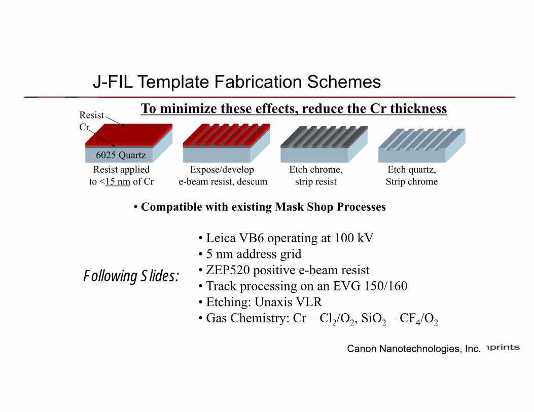
J-FIL Template Fabrication SchemesTo minimize these effects, reduce the Cr thickness
Resist appliedto <15 nm of Cr
Expose/develop e-beam resist, descum
Etch chrome,strip resist
Etch quartz,Strip chrome
6025 Quartz
ResistCr
• Leica VB6 operating at 100 kV• 5 nm address grid• ZEP520 positive e-beam resist• Track processing on an EVG 150/160• Etching: Unaxis VLR• Gas Chemistry: Cr – Cl2/O2, SiO2 – CF4/O2
• Compatible with existing Mask Shop Processes
Following Slides:

Canon Nanotechnologies, Inc.
ZEP520 Exposure/Descum
ZEP520A process latitude is excellent
40
60
80
100
120
140
300 400 500 600 700 800 900
ResistDescumCr EtchQuartz Etch
Exposure Dose (C/cm2)
Res
ist (
nm)
2.6nm change for every 20 seconds
-10
-5
0
5
10
0 20 40 60 80 100Descum Time (s)
Fina
l CD
Bia
s (n
m)
60 nm l/s80 nm l/s100 nm l/s

Canon Nanotechnologies, Inc.
Cr Process CD Results
• All results shown are for 80 nm features.
• Similar to observations made for increasing descum time, a positive CD change of 3.8nm per 20% of Cr overetch exists.
-10
-5
0
5
10
15
20
50 60 70 80 90 100 110 120 130Chrome Overetch (%)
Fina
l CD
Bia
s (n
m)
20 s descum40 s descum60 s descum
60% 80%
100% 120%

Canon Nanotechnologies, Inc.
FIB/TEM Feature Profile • Cross-sectioning the trenches
was done using a focused ionbeam tool in conjunction witha protective film stack toavoid extreme charging,sample drift, and surfacedamage.
• Using TEM measurements as a basis, sidewall angles of 150 nm features were calculated to be ~ 84°
• The measured etch depth of 98 nm compares extremely well to profilometer and AFM measurements.
PF031023-1.3PF031023-1.4

Canon Nanotechnologies, Inc.
Fabrication Window
• For 60 nm clustered features, thespaces measure ~ 4 nm overcoded size.
• The descum process increases CDby about the same magnitude.
• Resist erosion during Cr etchresults in approximately 7 morenanometers of bias.
• After quartz etch, CD bias is 1.5nm less than coded. The quartzsidewall angle is about 5° fromthe normal
• Final CD bias ends upapproximately 1 nm from codedafter the Cr hardmask is stripped.
• A 20 s descum coupled with a 110% Cr overetch was found to give the bestperformance in terms of CD control and line edge roughness.
-15-10
-505
10152025
ResistDescum
Cr EtchQuartz Etch
Final
CD
Bia
s fro
m C
oded
(nm
)
60 nm features80 nm features100 nm features

Canon Nanotechnologies, Inc.
Resist Descum Cr Etch Resist Strip Quartz Etch
60 nm
40 nm
30 nm
Pattern/Pattern Transfer Process
SPIE: Feb 2002

Canon Nanotechnologies, Inc.Canon Nanotechnologies, Inc.
Pattern Transfer Process Magnification : 150k
PMJ: April 2008

Canon Nanotechnologies, Inc.Canon Nanotechnologies, Inc.

Canon Nanotechnologies, Inc.Canon Nanotechnologies, Inc.
Electron Beam Pattern Generators
How do I get the best result from each tool?– Resolution– Line Width Roughness– CD uniformity– Image Placement– Write Time
There are two methods for generating patterns on a template:
1. Gaussian beam PGs: Great for unit process development and device prototyping
2. Variable Shaped Beam PGs: Needed for full field pattern generationand for image placement

Canon Nanotechnologies, Inc.Canon Nanotechnologies, Inc.
Gaussian Beam Pattern Generators

Canon Nanotechnologies, Inc.Canon Nanotechnologies, Inc.
ZEP520A Process Development
Exposure latitude of the resist was mapped as a function of feature bias
0.0
0.2
0.4
0.6
0.8
1.0
1.0E+01 1.0E+02 1.0E+03Dose (C/cm2)
Rel
ativ
e th
ickn
ess
rem
aini
ng
Xyleneso-XyleneAmyl acetateHexyl acetate
10
20
30
40
50
60
70
80
0 200 400 600Dose (uC/cm2)
Mea
sure
d re
sist
CD
(nm
)
40 nm 30 nm 20 nm
CD
80 nm pitch grating
Numbers next to curves indicate the digitized CD
Amyl Acetate developer provides a goodcombination of contrast and sensitivity
Exposure latitude is improves as biasing ofcritical features increases
Resist response was studied for a variety of different developers

Canon Nanotechnologies, Inc.Canon Nanotechnologies, Inc.
Development of ZEP520A resist
Sonication of developer bath Dilution of developer
– Equal mixture of amyl acetate with isopropyl alcohol
– 120 s puddle development– 60 s isopropyl alcohol rinse, dry
12
14
16
18
20
22
24
26
28
30
200 300 400 500 600
CD normalized dose (C/cm2)
CD (n
m)
18 nm
20 nm22 nm
24 nm22 nm half-pitch 18 nm half-pitch
Negative bias of 12 nm

Canon Nanotechnologies, Inc.Canon Nanotechnologies, Inc.
Imprint Resolution
22nm Fan-out
25nm Contacts 22nm half-pitch28nm half-pitch
20nm Half Pitch 20nm Half Pitch

Canon Nanotechnologies, Inc.Canon Nanotechnologies, Inc.
Line Width Roughness (LWR)
Variation in CD along the length of a line– Results in variation of MOS gate width– Affects device speed of individual transistors– Leads to IC timing issues
100 nm
2007 2010 2013 2016 2019
DRAMHalf-Pitch
65 45 32 22 16
LWR 3.4 2.4 1.7 1.2 0.8
ITRS Roadmap for LWR(nm, 3)
Future nodes have no known solutions.

Canon Nanotechnologies, Inc.Canon Nanotechnologies, Inc.
LWR Example: EUVL
LWR ~ 6-8 nm(SPIE)
Throughput requirements of EUVL require the use of fast chemically amplified resists– Low exposure doses required for throughputToo few photons: ~2 / nm2
Shot noise effects
RLS Trade-Off for Chemically Amplified Resists
Resolution vs. LWR vs. Sensitivity(Robert Brainard, Gregg Gallatin)
Reso
lutio
n
So, is imprint lithography immune to this problem?YES! And NO!!

Canon Nanotechnologies, Inc.Canon Nanotechnologies, Inc.
Pattern formation with J-FIL technology
Imprint Mask Fabrication Imprint Patterning
Resolution and LWR Throughput
Use non-CA resists for best resolution and LWR performance.
Utilize existing photomask infrastructure for fabrication and inspection.
CD, CDU, LWR, etc. of the patterned resist is determined by the template.

Canon Nanotechnologies, Inc.Canon Nanotechnologies, Inc.
LWR minimization at 22 nm
10
14
18
22
26
30
34
200 300 400 500 600 70022 nm normalized dose (C/cm2)
CD
(nm
)
0
1
2
3
4
5
6
LWR
, 3
(nm
)
CD
Parameter mean
Line Width, nm 23.36 1.28LWR <3>, nm 2.15 0.29
250 C/cm2: ~15 electrons / nm2
Gaussian E-Beam exposure at 100kV
LWR = 2.45 nm, 3
UnderExposed
LWR=3.29nm
CorrectlyExposed
LWR=2.45nm
OverExposed
LWR=4.27nm
22 nm HP

Canon Nanotechnologies, Inc.Canon Nanotechnologies, Inc.
30
32
34
36
38
40
42
44
46
30 32 34 36 38 40 42 44 46
Coded CD (nm)
Mea
sure
d C
D (n
m)
0
1
2
3
4
5
6
7
LWR
, 3
(nm
)
Template: CD and LWR Analysis
32nm
CD is linear from 32 to 44nm (to within about 5%) LWR is small, and independent of critical dimension
Parameter Mean, nm
Std. dev.,nm
Line Width 31.9 0.518LWR <3σ> 3.12 0.409Left LER <3σ> 4.326 0.447Right LER <3σ> 4.074 0.375Pitch 123.8 0.368
CD

Canon Nanotechnologies, Inc.Canon Nanotechnologies, Inc.
32nm Imprint Evaluation
Imprints #1 and #2 are taken from the same location
Imprint #3 is located 2mm from Imprint #1
32nm
Template: LWR = 3.1nm
#1LWR=2.55nm
#2LWR=3.05nm
#3LWR=2.60nm

Canon Nanotechnologies, Inc.Canon Nanotechnologies, Inc.LWR (nm, 3) = 2.05 1.79 2.40LER 1.01
30 nm design Field 6
LWR (nm, 3) = 1.91 2.15 2.56LER 1.76
40 nm design Field 11
30 nm and 40 nm design: LWR after etch into SiO2

Canon Nanotechnologies, Inc.Canon Nanotechnologies, Inc.
# lines measured: 170 LWRmean = 2.79nm LWRmin = 1.70nm LWRmax = 4.39nm 3 = 1.59nm
Summary of Line Width Roughness Data
0
1
2
3
4
5
15 20 25 30 35 40 45 50
E-beamTemplateImprintEtchFit
LWR
(nm
, 3si
gma)
Measured Feature Size (nm)
Canon Nanotechnologies, Inc.Canon Nanotechnologies, Inc.
Variable Shape Beam Pattern Generators

Canon Nanotechnologies, Inc.Canon Nanotechnologies, Inc.
Variable Shape Beam PGs (VSBs)System Architecture
J. Yashima et al, Photomask Japan 2007
NuFlare EBM 6000 plus
VSB systems are e-beam tools of choice for writing 4x photomasks
Old Wives Tale 9647: VSB tools are the correct choice if you need to write fast, but they don’t have great resolution

Canon Nanotechnologies, Inc.
VSB: Commercial Shops – CA Resists
Logic 80nm70nm
65 nm grating
EIPBN: May 2005

Canon Nanotechnologies, Inc.Canon Nanotechnologies, Inc.
Exposure Results: VSBs and ZEP520A
ZEP520A Resist Images: EBM-5000
35nm
35nm50nm40nm
45nm45nm
BACUS: September 2007
Canon Nanotechnologies, Inc.Canon Nanotechnologies, Inc.
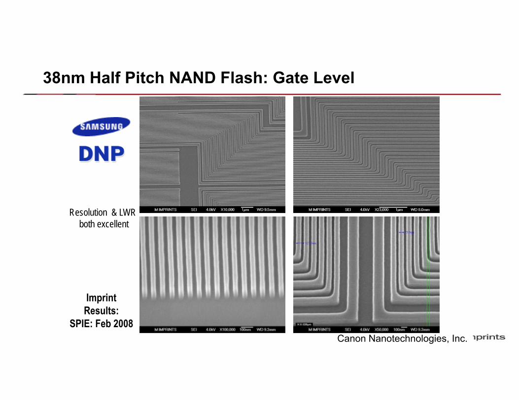
38nm Half Pitch NAND Flash: Gate Level
ImprintResults:
SPIE: Feb 2008
Resolution & LWR both excellent
Canon Nanotechnologies, Inc.Canon Nanotechnologies, Inc.
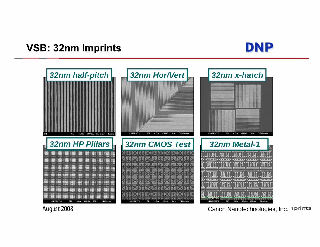
VSB: 32nm Imprints
32nm HP Pillars
32nm Hor/Vert 32nm x-hatch32nm half-pitch
32nm Metal-132nm CMOS Test
August 2008

Canon Nanotechnologies, Inc.Canon Nanotechnologies, Inc.
Sub-32nm from VSB PGs Imprint Mask
Imprints
24nm
26nm26nm24nm
28nm22nm

Canon Nanotechnologies, Inc.Canon Nanotechnologies, Inc.
Sub 20nm Masks from VSB PGs
Current NAND Flash devices are now being fabricated at half pitches of less than 20nm
How do we make a sub-20nm mask from a VSB tool?
OK, how can they do that?

Canon Nanotechnologies, Inc.Canon Nanotechnologies, Inc.
Density Multiplication
Density multiplication, also referred to as self aligned spacer double patterning is a standard process of record used to make high density NAND Flash devices
SADP
SAQP

Canon Nanotechnologies, Inc.Canon Nanotechnologies, Inc.
Some Density Multiplication Examples
SADP
SAQP

Canon Nanotechnologies, Inc.Canon Nanotechnologies, Inc.
CDU and Image Placement Comparison
GB
VSB
CD Uniformity Image Placement

Canon Nanotechnologies, Inc.Canon Nanotechnologies, Inc.
Write Time Patterns
Optical mask A (with OPC)
Template A (without OPC)
Optical mask B (with OPC)
Template B (without OPC)
Reticle APattern density:39.68%
Template APattern density:36.68%
Reticle BPattern density:
15.88%
Template BPattern density:11.78%

Canon Nanotechnologies, Inc.Canon Nanotechnologies, Inc.
Write Time Results
Pattern A Shot counts[G shot]
Writing time[hh:mm:ss]
Template, ZEP520A 223.7 22:51:434X Mask, FEP171 385.1 25:49:184X Mask, PRL009 770.3 62:24:05
Pattern B Shot counts[G shot]
Writing time[hh:mm:ss]
Template, ZEP520A 78.6 8:17:294X Mask, FEP171 336.5 22:48:374X Mask, PRL009 673.0 54:23:02

Canon Nanotechnologies, Inc.Canon Nanotechnologies, Inc.
When all is said and done, e-beam machines are slow!How can we make them write faster?
Probably good for fast mask writing, but maybe never for wafer writing
262,000 beams!!!

Canon Nanotechnologies, Inc.Canon Nanotechnologies, Inc.
Mask Replication
The lifetime of a mask is anticipated to be ~ 50,000 – 100,000 imprints
An e-beam written master mask will cost ~ $500K
If you wanted to print 1M wafers, you would spend ~ $500M on masks
Go share that strategy with a fab manager!!!
The solution: create a Master Template that can easily be replicatedMaster Daughter approachGood news! You can use an imprinter to make the Daughter Templates