Manufacturing and Investigating Objective Lens for ...
46
6 Manufacturing and Investigating Objective Lens for Ultrahigh Resolution Lithography Facilities N.I. Chkhalo, A.E. Pestov, N.N. Salashchenko and M.N. Toropov Institute for physics of microstructures RAS, GSP-105, Nizhniy Novgorod Russia 1. Introduction Current interest in super-high-resolution optical systems is related to the development of a number of fundamental and applied fields, such as nanophysics and nanotechnology, X-ray microscopy in the «Water window» and the projection nanolithography in the extreme ultraviolet (EUV) spectral range (Gwyn, 1998; Benschop et al., 1999; Naulleau et al., 2002; Ota et al., 2001; Andreev et al., 2000; Cheng, 1987). The great economical importance in applying the EUV lithography which, as expected, should replace the conventional deep ultraviolet lithography in commercial production of integrated circuits with topology at a level of 10-30 nm dictates a level of efforts carried out in the fields related to the technology. In the spectral range of soft X-ray and EUV radiation (nj=1-40 nm) this interest is accompanied by the intensive development of a technology for depositing highly reflecting multilayer interference structures (MIS) (Underwood & Barbee, 1981). In practice, the requirements for the shape of individual optical components and for the spatial resolution of optical systems are imposed on designing projection extreme ultraviolet lithography setups that operate at a wavelength of 13.5 nm (Williamson, 1995). EUV lithography should replace the conventional deep-ultra-violet lithography at 193-nm-wavelength radiation generated by excimer lasers in the commercial production of integrated circuits with a minimum topological-element size of 10-20 nm. The paper is devoted to the fundamental problems of manufacturing and testing substrates with fine precision for multilayer mirrors which surface shape, as a rule, is an aspherical one and that should be made with a sub-nanometer precision, to characterizing multilayer covers deposited onto these substrates which should not injure the initial surface shape and also to measuring with the sub-nanometer accuracy the wave-front aberrations of high- aperture optical systems, for instance, projective objectives. The main requirements for the shape and for the micro-roughness values of substrate surfaces attended to depositing MIS on them which are optimized for maximum reflectivity at a 13.5 nm wavelength are considered. The problem of roughness measurement of atomic- level smooth surfaces is discussed. The application of optical interferometry for characterizing the surface shape and wave-front aberrations of individual optical elements and systems is under consideration. A particular attention has been given to interferometers with a diffraction reference wave. The problem of measurement accuracy provided by the interferometers which first of all are connected with aberrations of the diffracted reference Source: Lithography, Book edited by: Michael Wang, ISBN 978-953-307-064-3, pp. 656, February 2010, INTECH, Croatia, downloaded from SCIYO.COM www.intechopen.com
Transcript of Manufacturing and Investigating Objective Lens for ...

6
Manufacturing and Investigating Objective Lens for Ultrahigh Resolution Lithography Facilities
NI Chkhalo AE Pestov NN Salashchenko and MN Toropov Institute for physics of microstructures RAS GSP-105 Nizhniy Novgorod
Russia
1 Introduction
Current interest in super-high-resolution optical systems is related to the development of a number of fundamental and applied fields such as nanophysics and nanotechnology X-ray microscopy in the laquoWater windowraquo and the projection nanolithography in the extreme ultraviolet (EUV) spectral range (Gwyn 1998 Benschop et al 1999 Naulleau et al 2002 Ota et al 2001 Andreev et al 2000 Cheng 1987) The great economical importance in applying the EUV lithography which as expected should replace the conventional deep ultraviolet lithography in commercial production of integrated circuits with topology at a level of 10-30 nm dictates a level of efforts carried out in the fields related to the technology In the spectral range of soft X-ray and EUV radiation (=1-40 nm) this interest is accompanied by the intensive development of a technology for depositing highly reflecting multilayer interference structures (MIS) (Underwood amp Barbee 1981) In practice the requirements for the shape of individual optical components and for the spatial resolution of optical systems are imposed on designing projection extreme ultraviolet lithography setups that operate at a wavelength of 135 nm (Williamson 1995) EUV lithography should replace the conventional deep-ultra-violet lithography at 193-nm-wavelength radiation generated by excimer lasers in the commercial production of integrated circuits with a minimum topological-element size of 10-20 nm The paper is devoted to the fundamental problems of manufacturing and testing substrates with fine precision for multilayer mirrors which surface shape as a rule is an aspherical one and that should be made with a sub-nanometer precision to characterizing multilayer covers deposited onto these substrates which should not injure the initial surface shape and also to measuring with the sub-nanometer accuracy the wave-front aberrations of high-aperture optical systems for instance projective objectives The main requirements for the shape and for the micro-roughness values of substrate surfaces attended to depositing MIS on them which are optimized for maximum reflectivity at a 135 nm wavelength are considered The problem of roughness measurement of atomic-level smooth surfaces is discussed The application of optical interferometry for characterizing the surface shape and wave-front aberrations of individual optical elements and systems is under consideration A particular attention has been given to interferometers with a diffraction reference wave The problem of measurement accuracy provided by the interferometers which first of all are connected with aberrations of the diffracted reference
Source Lithography Book edited by Michael Wang ISBN 978-953-307-064-3 pp 656 February 2010 INTECH Croatia downloaded from SCIYOCOM
wwwintechopencom
Lithography
72
wave is under discussion The reference spherical wave source based on a single mode tipped fiber with a sub-wave exit aperture is fully considered The results of studying this source and the description of an interferometer with a diffraction reference wave made on the base of the source are given The application of this interferometer for characterizing spherical and aspherical optical surfaces and wave-front aberrations of optical systems is illustrated The achieved abilities of the interferometric measuring the surface shape of optical elements with a sub-nanometer accuracy make possible to develop different methods for correcting the optical element surfaces initially made with traditional for optical industry precision (root-mean-square deviation from the desired one about RMS asymp 20-30 nm) to the same sub-nanometer accuracy Two methods of a thin film depositing and an ion-beam etching through the metallic masks produced on evidence derived from the interferometric measurements are considered for the surface shape correction of optical elements The dependences of the etching rate and the dynamics of the surface roughness on the ion energy (neutral in the case of fused silica etching) and the angle of the ions incidence to the corrected surface are presented The final results obtained when correcting substrates for multilayer imaging optics for a 135 nm wavelength are reported Much attention is paid to the final stage of a mirror manufacturing and depositing a multiplayer interference structure onto the substrate reflecting a short wavelength radiation Some peculiarities of the deposition technology as applied to the mirrors with ultra-high precision surface shape are discussed Methods for compensating an intrinsic mechanical stress in the multilayer films developed in IPM RAS are described In conclusion the problems on the way to manufacture atomic smooth ultrahigh precision imaging optics for X-ray and EUV spectral ranges yet to be solved are discussed
2 The main requirements for the shape and for the micro-roughness of substrate surfaces
According to the Mareshal criterion to achieve the diffraction limited resolution of an optical system it is necessary that a root-mean-square distortion of the system wave front RMSobj must satisfy this ratio (Born amp Wolf 1973)
14objRMS λle (1)
where λ is a wavelength of light Since the errors (distortions) of elements of a complex optical system are statistically independent quantities the required accuracy RMS1 of manufacturing an individual optical component is
1 (14 )RMS Nλle sdot (2)
where N is a number of components in the optical system For instance in the case of a six-mirror objective typical of EUV lithography at the wavelength of λ=135 nm the reasonable error of individual mirror RMS1 should not exceed 04 nm Let us consider the influence of objective aberrations on the image quality by the example of imaging of 150 nm width strips by means of Schwarzschild-type objective made up of two aspherical mirrors and providing linear demagnification coefficient of x5 Fig 1 The calculation was done with the help of ZEMAX code at a wavelength of 135 nm On the left in Fig 1 a picture of strips to be imaged and their light emission is given
wwwintechopencom
Manufacturing and Investigating Objective Lens for Ultrahigh Resolution Lithography Facilities
73
Fig 1 A projection objective diagram made up of a convex M1 and a concave М2 aspherical mirrors An exit numerical aperture is NA=03 and a linear demagnification coefficient is x5
The strips images and light intensity distributions in the image plane corresponding to different from RMS=32 to RMS=4 values of the objective wave aberrations are given in Fig 2 The figure shows that at the aberration of 4 the image has fully disappeared At RMS=14 we have the image contrast (ratio of intensities from the minimum to the maximum) at a level of 05 At the aberration RMSlt24 the image contrast no longer depends on the aberration and is determined only by a numerical aperture of the objective In such a manner a reasonable aberration is a value at the level of RMSasymp30 or 045 nm In view of Eq (2) the requirements for the quality of individual mirrors are stronger at a level of 02 nm
Fig 2 Images of lines and light intensity distributions in the image plane depending on an objective wave aberration =135 nm a) ndash root-mean-square aberration RMS=32 b) ndash RMS= 24 с) ndash RMS= 14 d) ndash RMS= 8 е) - RMS= 4
The problem of manufacturing mirrors with a sub nanometer surface shape precision for EUV lithography is complicated by a number of factors First because of considerable intensity losses due to the reflection of radiation with a wavelength of =135 nm from MIS a number of mirrors in an optical system must be minimized For this reason to increase a field of view and to achieve a high space resolution of an objective one has to use aspherical surfaces with high numerical apertures Second a small radiation wavelength and a huge number of interfaces in multilayer interference structure participating in the reflection process impose rigid requirements on the interfacial roughness which in turn is substantially determined by the surface roughness of a substrate (Warburton et al 1987 Barbee 1981 Chkhalo et al 1993)
wwwintechopencom
Lithography
74
The interfacial roughness with a root-mean-square height σ effects in decreasing both a reflection coefficient of the multilayer mirror and the image contrast because of the scattering of radiation The estimation of the total integrated scatter (TIS) can be done as follows
21 exp (4 )TIS πσ λ⎡ ⎤= minus minus⎣ ⎦ (3)
where is a radiation wavelength For instance if the integral scattering of an individual mirror is to be lower than 10 the interfacial roughness must be at a level σle03 nm The more precise analysis shows that everywhere over the region of space wavelengths of the Fourier transform of the reflecting surface (from fractions of nanometer up to tens of millimeters) the root-mean-square of the surface distortions should be at a level RMSle02 nm (Williamson 1995 Sweeney et al 1998 Soufli et al 2001)
3 Surface roughness measurement methods
As is seen from ratio (3) among the factors having effect on reflection coefficients of MIS a substrate surface roughness plays a significant role There exist a few methods for surface roughness measurements with heights of nanometer and sub-nanometer level at present Among them the atomic force microscopy (Griffith amp Grigg 1993) and diffusion scattering of hard X-ray radiation (Sinha et al 1988 Asadchikov et al 1998) are mostly developed and widely used A number of papers report a good agreement of experimental data about the surface roughness obtained by both methods (Kozhevnikov et al 1999 Stone et al 1999) It is necessary to mention a recently well-established method of a surface roughness measurement by means of an optical interference microscopy (Blunt 2006 Chkhalo et al 2008) In this case the producers of the micro interferometers and opticians who use these instruments report about roughness measurement precision up to 001 nm In particular it is stated that super-polished quartz substrates produced by General Optics (USA) have the roughness at a level of 007 nm (Website GO 2009) But relatively low lateral resolution characteristics of the methods substantially limit the spectrum of space frequencies of a surface roughness to be registered from the high-frequency side that impairs their capabilities when measuring super-polished substrates attended for short-wavelength optics For instance in Fig 3 where the angular dependence of a scattered intensity of X-ray radiation with a wavelength of =0154 nm from a fused silica super-polished substrate is presented one can see that at the angle about 06ordm the scattered intensity is about 10-6 of the incident one down to a detector noise For the X-rays with =0154 nm the angle 06deg corresponds to the scattering on surface space frequencies with a wavelength of 28 microm This resolution is comparable with the lateral resolution of the interference microscopes and ranks below the resolution of atomic force microscopes Therefore noted in some papers a good agreement of experimental data about the surface roughness obtained by these methods can be explained only as follows In spite on the fact that the radius of a cantilever of the atomic-force microscope may be at the level of a few tens of nanometers there exist some other factors such as the true radius of a probe the peculiarities of the probe moving vibrations mathematic processing of experimental data and others which are specific for each instrument for each laboratory which decrease the instrumental lateral resolution
wwwintechopencom
Manufacturing and Investigating Objective Lens for Ultrahigh Resolution Lithography Facilities
75
Fig 3 An angular dependence of scattered intensity of X-ray radiation from a fused silica substrate taken with X-ray diffractometer PhilipsrsquoExpert Pro at a wavelength of =0154 nm Detector angle is fixed θd=06deg
The most reliable data about the roughness of atomic-smooth surfaces as we assume give a method based on the analysis of angular dependencies of specular reflection coefficients of X-ray radiation The method was proposed in (Parratt 1954) and was widely used in Refs (Chkhalo et al 1995 Protopopov et al 1999 Bibishkin et al 2003) The influence of the roughness σ on the angular dependence of the reflection coefficient R(θ) was taking into account with the help of attenuation coefficient of Nevot-Croce ( Nevot amp Croce 1980) as follows
2 2
22
16( ) ( ) exp sin Re sinidR R
π σϑ ϑ ϑ ϑ χλ⎧ ⎫= sdot minus sdot sdot +⎨ ⎬⎩ ⎭ (4)
where Rid(θ) is an angular dependence of the reflection coefficient on the ideal surface and is calculated with the Fresnelrsquos formulae λ is a radiation wavelength and is a dielectric susceptibility of the substrate material In the calculations the material optical constants were taken from (Palik 1985) The advantages of this method are of a ldquosmallrdquo size of the probe the radiation wavelength is comparable with the roughness value and the lack of limitation about the registered spectrum of space frequencies of a surface roughness from the high-frequency side because in ldquozerordquo order of diffraction all radiation losses are taking into account From middle-frequency side the registered spectrum is limited by the width of the detector slit and is about 30 microm But it is not the principal restriction since in this range the interference microscopes operate well An example of applying this method for the characterization of a fused silica substrate produced by General Optics (USA) in 2007 with a factory specified roughness value of 008 nm is given in Fig 4 As one can see the best fit of the experimental curve (dots) is observed for the surface roughness lying in the range of σ = 03ndash04 nm That is 4-5 times more as compared with the specified value Exactly the same experimental data were obtained in independent measurements made in Institute of crystallography Russian academy of sciences in Moscow
wwwintechopencom
Lithography
76
Fig 4 Angular dependencies of reflection coefficients of radiation with λ=0154 nm from a fused silica substrate made by General Optics dots correspond to experiment solid lines are calculations corresponding to different roughness values
The investigation of this substrate by means of an atomic-force microscopy carried out in our institute has shown a strong dependence of measured roughness on the probe size When we use Si-cantilever the measured roughness was about 008 nm but with a wicker the value has increased up to 016 nm So this direct comparison of the application of X-ray reflection and atomic force microscopy for atomic-smooth surface roughness measurement indicates that the latter method gives an underestimated value of the roughness A serious disadvantage of the specular X-ray reflection method is that it allows studying only flat samples while components of imaging optics have concave and convex surface shapes Therefore in practice for evaluating the surface roughness of nonplanar samples it makes sense to use the atomic force microscopy method taking into account the calibration of X-ray reflection made with flat substrates In conclusion it should be noted that a large body of research done with the help of the x-ray specular reflection method to measure a surface roughness showed that a number of substrates fabricated in different countries had a minimal surface roughness 02-03 nm and included crystal silicon used in electronic industry The minimal surface roughness of fused quartz substrates were in the range of 03-04 nm except for the case (Chkhalo 1995) where the roughness of 025 nm is reported
4 Investigating the surface shape by means of optical interferometry
Optical interferometry is one of the most powerful and widely used method for measuring a surface shape of optical components and wave front aberrations of complex systems in the industry The main advantages of the inetrferometry are the simplicity and high accuracy of the measurements The investigation technique is based on the analysis of a light intensity distribution over interference patterns In this paragraph the basic principles of a surface shape and wave front distortions of optical component and system reconstruction with the use of data obtained by optical interferometers are described Both types of interferometers
wwwintechopencom
Manufacturing and Investigating Objective Lens for Ultrahigh Resolution Lithography Facilities
77
are considered conventional utilizing reference surfaces and diffraction using as a reference a spherical wave appeared due to the diffraction of light on a wave-sized pin-hole
41 Shape reconstruction and interferometry utilizing reference surfaces At present a gamma of interferometers is used in an optical industry including Fizeau and Twyman-Green interferometers which stand out because of their simplicity in operation high accuracy and universality is developed A detailed description of these instruments can be found in many books for instance (Malacara 1992 Okatov 2004) Independently on an optical scheme in this type of instruments the interference patterns are detected which appear as a result of the interaction of two waves reflected from studied ES (a surface with defects in Fig 5) and from reference ER (top surface in Fig 5) surfaces As a result the fringes
Fig 5 A fringe pattern formation by interfering of two waves reflected from a surface under study (bottom) and a reference (upper) one
of so called ldquoequal thicknessrdquo are observed A defect on the surface under study marked in Fig 5 by symbol z with a height of h gave rise the phase shift of the reflected light according to
2 2 hπ δ λΔ = sdot (5)
where λ is a wavelength The corresponding fringe banding z induced by the deviation of the studied surface from the reference can be found from the ratio
( 2) h z zδ λ δ= sdot (6)
These expressions in particular allow to see that the defect with the height of λ2 corresponds to one fringe in the interference pattern When the defects on the studied surface are absent the fringes make a system of equidistant straight lines In such a manner the interference pattern uniquely determines the local shape deviations of the surface under study from the reference So the task of the surface shape reconstruction needs looking for a mathematical model which will fit the experimental data the best
( ) ( )W x y h x y= Δ (7)
where ( )h x yΔ is the surface deformation in respect to the reference and being a function of coordinates on the surface x yisinΩ Ω is an operating range of the surface As a rule the
wwwintechopencom
Lithography
78
sought-for function (Braat 1987) is written in terms of some basis of functions and its description reduces to finding a set of the series coefficients ck
( ) ( )k kk
W c α=sumr r (8)
where r is a radius-vector of a point on the surface and ( )kα r is a set of basis functions Mostly common polynomials orthogonal on some area 0Ω are chosen as the basis For instance for the circular area these are Zernike polynomials which are widely used in optics (Rodionov 1974 Golberg 2001) The orthogonality of the polynomials results in the fact that each term of the series makes a contribution independent on the remaining terms into the mean-square of the wave front deformation Since the representation of the investigated function is global any local dilatation when approximating is smoothed thus distorting global view of the function Besides when reconstructing the surface shape it is important to evaluate not only the global surface shape but local errors too From this it follows that the mathematical model should be oriented on the description of the surface shape not only globally but locally too In the framework of this paper this dilemma was solved by introducing local deformations additionally to the global description (8) of the surface deformation function
0( ) ( ) ( )k k mj jk m j
W c cα β⎡ ⎤= + sdot minus⎢ ⎥⎢ ⎥⎣ ⎦sum sum sum mr r r r (9)
where cmj and j are coefficients and ldquospecialrdquo basis functions describe a m-th local deformation with the center in the point with the coordinate of r0m It is significant that the set of functions k(r) and j(r-r0m) are different in general case because the described function W(r) should not be interrupted in the range of definition It is the reason why the ldquospecialrdquo functions j(r-r0m) must be finite should not have discontinuity and their values at the definition range boundary must be equivalent to zero An algorithm of searching for the expansion coefficients of the surface model (9) was performed in two stages At the first stage the global surface shape error is approximated according to the (8) model At the second stage the residual local surface deformations are approximated by the right part of the expression (9) In our case the global description of the surface shape errors is performed with the help of Zernike polynomials WZ() and the residual local dilatations ndash by using the apparatus of local splines WS() which advantages when describing the optical surface deformations are analyzed in (Archer 1997 Sun et al 1998) in details
0 0 0 0
0 0
( ) ( ) ( ) ( )cos( ) ( )sin( )
( sin( )) ( cos( ))
Pz n Pz nm m
Z S nm n nm nn m n m
k k
i P j P ijS Si j
W W W c R m s R m
B B P
ρ ϕ ρ ϕ ρ ϕ ρ ϕ ρ ϕρ ϕ ρ ϕ
= = = =
= =
= + = + ++ sdot sdot sdot
sumsum sumsumsumsum (10)
where and are polar coordinates of the point on the surface cnm and snm are the expansion coefficients ( )m
nR ρ are radial Zernike polynomials BiPs is the basic function of the -spline of the order of pS on i-th interval of y coordinate and BjPs ndash is the basic function of the -spline of the order of pS on j-th interval of x coordinate and Pij corresponds to the
wwwintechopencom
Manufacturing and Investigating Objective Lens for Ultrahigh Resolution Lithography Facilities
79
points of control of the spline A number of works (Rodionov 1995 Swantner amp Weng 1994) are devoted to the methods for determining the coefficients of the mathematical model of the surface shape deformation function (10) by using interferometric data In present work algorithms and programs developed in (Gavrilin 2003) are used Currently available methods of digital registration and mathematical processing of interferograms allow reconstructing the surface shape (wave front aberrations) in respect to the reference surface Fig 5 with the accuracy up to 10000 where is an operating wavelength of the interferometer However the guaranteed surface shape accuracy of the reference in the root-mean-square (RMS) does not exceed 30 ndash 20 (Website Zygo 2009) that is two orders of magnitude worse than required for instance for projection nanolithography optics A substantially better situation is observed when studying surfaces at typical scales lower than 1 mm At these scales the accuracy of the reference surfaces is better than 1000 that allows measuring the surface shape deformations with the sub-nanometer accuracy On this basis a number of micro-interferometers with a digital fringe registration has been developed in the last few years (Blunt 2006 Chkhalo et al 2008 Website Veeco 2009 Website Zygo 2009) Below the spectrum of space wavelengths on the surface under study to be registered and where the surface shape measuring by interferometers with the sub-nanometer accuracy is limited by the lateral resolution of a microscope is given typically lies in the range of 03-1 microm
42 Interferometers with a diffraction reference wave The problem of conventional interferometers using the reference surfaces is solved by the application of interferometers with a diffraction wave as the reference proposed by VP Linnik in 1933 (Linnik 1933) The proposal is based on the theoretical fact that when a flat electromagnetic wave falls onto a pin-hole with a diameter comparable with a wavelength in an opaque screen consisting of a zero-thickness superconducting material diffracted behind the screen wave in a far wave zone is an ldquoidealrdquo sphere (Born amp Wolf 1973) This feature of the light diffraction was used as the basis for developing interferometers of this type The first interferometer attended to the investigation of optics with sub-nanometer accuracy for the EUV nanolithography has been made by GE Sommargren in 1996 As a source of the reference spherical wave he used a single-mode optical fiber with a core diameter (exit aperture) of about 4-5 microm The objective for a projection scheme of a EUV-nanolithographer was tested with the help of the interferometer (Sommargren 1996) The author evaluated the measurement precision in terms of the RMS at the level of 05 nm With a high-coherence laser the interferometer allowed testing a surface shape of individual optical elements The main disadvantage of the interferometer was a ldquobigrdquo source size A numerical aperture where the diffracted wave still remains ldquoan ideal sphererdquo is determined by expression NAref ltλd and in the case of λ=05 microm and d=5 microm corresponds to NAreflt01 Partly the low-aperture problem is solved at the expense of stitching measured data over different areas of the studied substrate or objective Along with the apparent loss of a measurement accuracy when using the stitching procedure there exists one even more serious disadvantage of using low-aperture interferometers associated with a strong irregularity of interferogram illumination Fig 6 demonstrates how the illumination irregularity results in error when determining the position of the fringe extremum In other words along with the apparent
wwwintechopencom
Lithography
80
loss of measurement accuracy connected with the stitching low-aperture interferometers have a significant systematical error induced by strong intensity anisotropy of the reference wave Therefore the recent trends are toward increasing the use of diffraction on man-made pin-holes in an opaque screen Modern microelectronic technologies provide manufacturing high-quality low-edge roughness pin-holes with diameters down to 40-50 nm
Fig 6 Shift of determined position of fringe maximum (systematic error) caused by the illumination irregularity
Such pin-holes are applied in diffraction interferometers operating at the working wavelength of a EUV nano-lithographer λ=135 nm which are installed on undulators of the last generation synchrotrons in USA and Japan (Naulleau et al 2000 Murakami et al 2003) An interferometer circuit installed on ALS (Berkeley USA) is given in Fig 7
Fig 7 Optical scheme of interferometer with diffraction reference wave installed on synchrotron ALS in Berkeley USA The picture is taken from (Medecki et al 1996)
The device operates in the following way The radiation falls onto a small pin-hole Gap installed on the lens object plane under study A diffracted ldquoidealrdquo spherical wave passing through the lens is distorted according to its aberrations and is collected in the image plane On the radiation way in-between the lens and the image plane a diffraction grating is installed which splits the wave-front into two ones corresponding to zero and to 1-st diffraction orders The zero-order radiation passes through the hole which diameter is big enough and exceeds a focusing spot thus preventing the distortion of the wave front The 1-st order beam is focused onto a small-size pin-hole Due to the diffraction behind the
wwwintechopencom
Manufacturing and Investigating Objective Lens for Ultrahigh Resolution Lithography Facilities
81
screen ldquoan idealrdquo spherical wave is generated The reference wave expands toward a CCD-camera where it interferes with a wave passed through the lens under test The measurement accuracy provided by the interferometer will be discussed later when comparing with our interferometer As we can see such interferometers are efficiently used for the final characterization of wave-front aberrations of objectives for EUV radiation At manufacturing stages of substrates and mirrors the producers of the optics usually use optical diffraction interferometers The experimental study of capabilities of point diffraction interferometers operating with a visible light has demonstrated a number of factors reducing the measurement accuracy Particularly systematic discrepancy of experimental data when studying the same optics with the help of visible and EUV light interferometers is observed (Goldberg et al 2002) All of this stimulated to study the way how finite conductance and thickness of the screen material have an effect on amplitude-phase characteristics of the diffracted wave behind the screen and correspondingly on the interferometer measurement accuracy In work (Chkhalo et al 2008) the calculations of the amplitude-phase characteristics of the diffracted field behind the screen in the far-field zone have been carried out They used the solution of a task about the field of a point source located above a half-space with arbitrary properties and covered with a film of any thickness and arbitrary optical constants given in (Dorofeyev et al 2003) Fig 8 illustrates the statement of the problem The diffraction of a flat wave on a circular hole with the radius of a in a film with thickness of hf and the inductivity of f in medias with parameters and 1 was considered The field was calculated behind the screen at Zgt0 on a spherical surface with a fixed radius R0=10 cm The radius R0 was chosen from practical reasons but its value does not produce any effect on the community of the result since the calculation was done for a case krgtgt1 where k=2λ is a wave vector of the diffracted wave in a point with the radius-vector r
Fig 8 Sketch of the geometry of the problem where hf is the thickness of the film heff is an effective film thickness (characterized by the skin-layer) d is the diameter of a hole 1 and f are the dielectric constants of the film and the medias θ1 and θ2 are the angles of diffraction Incident wave is schematically shown by the arrows
The results of the calculations as compared with the solution of classical task of diffraction on zero-thickness superconducting screen have shown that most real electrodynamical
wwwintechopencom
Lithography
82
characteristics of the screen material have an effect on phase characteristics of the diffracted field The calculation of the phase distortions was carried out for the films of aluminum molybdenum tungsten and a number of other materials The results of numerical calculations shown in Fig 9 represent a relative phase deviation on meridional angle of the diffracted scalar field in the case of aluminum different thickness films characterized by dielectric constant Alasymp-542-i218 at the wavelength 633 nm as compared with the case of a perfect screen |Al|rarrinfin The phase incursion ∆(θ) is expressed in nanometers The radius of the hole in the films was а=150 nm A case of free standing (=1=1) films was considered It is evident that the larger the meridional angle the larger is the phase deviation of the diffracted field in the case of a realistic screen We connect the result with an additional phase accumulation due to the field propagation through the real film at larger meridional angles (see Fig 8 for a qualitative clarification) We did not find a thickness dependence on the phase accumulation in the range of lthflt1000 nm where is a skin-layer because the phase can be effectively accumulated only inside the skin-layer The transitions hfrarr0 and |Al|rarrinfin |Al|rarrinfin or hfrarr0 led to the known textbook examples The corresponding diffraction fields for such idealized problems perfectly coincide with those of a spherical phase front
Fig 9 A relative phase deviation ∆(θ)=((0)-(θ))λ2 on meridional angle of the diffracted field in a case of Al different thickness film (Alasymp-542-i218) at the wavelength 633 nm on a spherical surface R0=10 cm the hole radius is а=150 せす
Other mechanisms of the phase distortion can be associated with the excitation of waveguide and surface modes in a plane layer and with a diffraction of such modes by a hole followed by their radiative decay Since the dielectric constant of all materials in soft X-ray and EUV ranges are close to unity Re()asymp1 corresponding phase distortions are minimal It is one of the reasons why the quality of the diffracted reference wave in EUV region has a better result in a higher measurement precision The carried out calculations have shown (see Fig 10) that the angular dependencies of the phase distortions on the meridional angle weakly change for different materials The only exception is osmium for which the phase deformation was extremely low Optical constants of materials used in these calculations were taken from (Palik 1985)
wwwintechopencom
Manufacturing and Investigating Objective Lens for Ultrahigh Resolution Lithography Facilities
83
Fig 10 Angular dependencies of the phase distortions on the meridional angle for different materials
By this means a fundamental limitation of the point diffraction interferometer measurement accuracy is caused by the aberrations of the reference spherical wave induced by the interaction and propagation of secondary waves through the screen material These aberrations are liable to reach a few nanometers depending on the angular aperture If we take into account the polarization characteristics of the light the aberration of the reference wave increases a few times depending on azimuth angle (Dorofeev 2009) The quality of a diffracted wave strongly depends on wave aberrations of preliminary optics focusing the laser beam and the accuracy of adjusting the laser beam axis in respect to the pin-hole center (Otaki et al 2002) All these limit the working aperture of the interferometer and result in the necessity of testing high-aperture optics zones The following stitching procedure of the zonal data raises additional errors All of these disadvantages hinder to widespread use of the point diffraction interferometers in an industry Taking into account all of these problems and limitations the problem of searching for alternative and more perfect methods for the spherical wave generation becomes very urgent
5 Spherical wave source on the basis of tipped fiber
The sources of the spherical wave based on tipped down to a sub-wave exit aperture of the single mode fibers are free from the many of mentioned above problems The application of such fibers as a reference spherical wave source for the point diffraction interferometers has been proposed in (Klimov et al 2008) In Ref (Chkhalo et al 2008) the aberrations of the wave generated by the sources at the wavelength of He-Ne laser =633 nm have been studied These investigations have demonstrated a number of advantages of spherical wave sources as compared with the conventional ones based on a pin-hole in an opaque screen One of the advantages is connected with the fact that in the optical fiber the eigenmodes are excited and correspondingly the quality of the diffracted wave does not depend on aberrations and the mechanical adjustment of the preliminary optics A high degree of homogeneity of the diffracted wave (dgt1) is combined with a high intensity because the light is input into the fiber using high-efficiency methods through a 5-
wwwintechopencom
Lithography
84
microm-diameter core The convex shape of the source Fig 11 decreases the ldquotiprdquo effect bound to the interaction of the off-axis rays with a metallized part of the fiber along the perimeter of the exit aperture The lack of a flat screen around the source significantly decreases diffracted wave distortions connected with the light polarization The well developed methods for handling optical fibers make it possible to easily control the polarization parameters of the diffracted radiation and implement various schemes for interference measurements For instance two or even more coherent sources can be organized with the given polarization of each other
Fig 11 Photographs of the fiber based source taken with scanning electron microscope (marked as a) and b)) and the source with on optical connector
The quality of the diffracted wave of the tipped fiber based source was studied with an interferometer (Kluenkov et al 2008) at two wavelengths =633 nm (He-Ne laser) and =530 nm (second harmonic of Nd-YAG laser) As opposed to the former experiments when in the measurement scheme an optical observation system collected the interfering fronts onto the CCD-camera in present work the data obtained by the direct detection of the fronts on the window-free CCD-camera are given As the experiments showed both the observation systems and even a thin glass window introduce a significant at the level of parts of nanometer error into the measurements
Fig 12 Experimental setup for studying the wave front deformations of the tipped fiber based sources of spherical wave 1 is a laser 2 is a system for input the light into the fiber 3 is a single mode fiber optics coupler 4 is a polarization controller 5 are sources under study 6 is a CCD-camera and 7 is a computer
wwwintechopencom
Manufacturing and Investigating Objective Lens for Ultrahigh Resolution Lithography Facilities
85
The new experimental setup is given in Fig 12 Polarization controllers (item 4 in Fig 12) allow to transform an elliptical polarization of the light at the output of the sources into a linear one as well as to superpose the polarization planes which provide the best contrast of the interference pattern The distance between the sources determining the fringe number (a wedge between two interfering wave fronts) was varied in the range of 1-10 m The measurements were carried out for different angles between the source axes The numerical aperture was varied by approaching (moving off) the CCD camera in respect to the sources A typical interferogram and a wave aberration map obtained in the experiments are shown in Fig 13 The operating wavelength was =530 nm
Fig 13 A typical interferogramm and a wave aberration map observed in the experiments obtained at a wavelength =530 nm
The measured dependencies of the wave deformation RMS on numerical aperture NA of this couple of sources are given in Fig 14 The pictures correspond to the measurements in small (left) and in large (right) numerical apertures Left graphs on both pictures correspond to the experimental data The data obtained with the interferometer installed on the synchrotron ALS in Berkeley USA are marked by stars The interferometer using a pin-hole in an opaque screen as a reference spherical wave source operates at the wavelength =135 nm and is considered as a reference for the measurement accuracy among the point diffraction interferometers (Naulleau et al 1999) It is clearly seen from the pictures that wave front aberrations of the source developed in this work are even less as compared with the ALS-sources despite a longer operating wavelength When analyzing the obtained experimental data there is a need to pay attention to two facts bull Relatively ldquohighrdquo of order λ1000 total aberration of the diffracted waves is observed
at large numerical apertures (NAasymp03) bull Regular structure (symmetry) of the wave front deformation map is clearly seen Such maps and statistical values of the deformations are practically found for all couples of so called ldquohigh qualityrdquo sources The wedge direction between interfering fronts (a line passing through the sources) represents itself as the axis of the symmetry Particularly the deformation map can be put ldquohorizontallyrdquo by turning the wedge through 90 degrees All of this points to the presence of an aberration caused by some kind of physical reason rather than by technological fluctuations This aberration rises with the increase of the observation angle just as it is shown in Figs 9 and 10 In case of understanding the physical nature of this aberration it can be taken into account when reconstructing the true wave deformation (surface shape) that results in increasing the working aperture of the interferometer by a few times
wwwintechopencom
Lithography
86
Fig 14 Averaged over 9 measurements total wave front deformations of couple of the fiber based spherical wave sources depending on numerical aperture (left graphs in both pictures) and ALS-data (Naulleau et al 1999) (stars) Working wavelength is =530 nm First picture corresponds to lower and right ndash to the higher numerical apertures The right graphs in the pictures are corrected according to the geometry of the experiment
This fact of the uniform angular dependence of the aberration let us interpret in a new manner the measurement data obtained in ALS and in our experiments In the Youngrsquos experiment carried out in ALS the least distorted parts of the diffracted waves round their own axes interfere Correspondingly RMS of the aberration is calculated over the range of the cone limited by the numerical aperture NA Opposite to that in our case side parts of the wave fronts interfere Fig 12 in the range from zero degree up to a double value of the angular aperture of the wave front In other words in the search for the wave front aberration RMS the averaging is performed over a double numerical aperture 2NA Therefore the measured dependences presented in Fig 14 (left graphs) can be corrected in the manner as it is shown by arrows (right graphs) As it is seen from the picture the source of the reference spherical wave based on a tipped single mode fiber has a substantially lower wave front aberration and a higher working aperture as compared with the conventional one based on pin-hole in an opaque screen
6 Diffraction interferometer based on a single mode fiber with the sub-wave exit aperture
On the basis of a tipped fiber source of the reference spherical wave the laboratory sample of an interferometer has been developed and manufactured which optical scheme and photo are presented in Figs 15 and 16 The interferometer is installed in a basement thermostated room on a bearer separated from the house footing For the additional protection against vibrations the instrument is installed on 12 bellows under 16 bar pressure Since the measurement accuracy is extremely high the turbulent air flowing inside the interferometer and effecting optical paths along the rays can introduce additional errors To solve these problems the interferometer is placed into a vacuum chamber which is pumped out down to a pressure of 1 Pa
wwwintechopencom
Manufacturing and Investigating Objective Lens for Ultrahigh Resolution Lithography Facilities
87
Fig 15 Optical scheme of the interferometer 1 ndash PC 2 ndash registering system 3 ndash observing system 4 ndash source of spherical wave 5 ndash flat sharp-edge mirror 6 ndash three-axes-controlled precision bench 7 ndash tested concave surface 8 ndash single mode optical fiber 9 ndash polarization controller 10 ndash laser
Fig 16 Photograph of the vertical vacuum interferometer
wwwintechopencom
Lithography
88
The optical scheme shown in Fig 15 corresponds to the interferometer for studying concave spherical or weakly aspherical surfaces The spherical wave source (item 4 Fig 15) is mounted on a high-precision three-axis-controlled bench (item 6 Fig 15) in the direct in a distance of several micrometers proximity from the flat mirror (item 5 Fig 15) The reference spherical wave which after reflecting from the studied surface (item 7 Fig 15) carries the information about its form is focused on a flat mirror and being reflected from it goes into the CCD registering system where it interferes with a part of the reference front directly propagating to the detector The main disadvantage of this scheme is connected with the fact that the investigated sample is irradiated by the most distorted side part of the wave front that practically halves the interferometer operating numerical aperture For solution of this problem in (Kluenkov et al 2008) the scheme of the interferometer with two low-coherent sources of the reference spherical waves has been proposed (Fig 17) In this scheme one source forms the spherical wave laquoSpherical wave 1raquo irradiating the investigated surface while the spherical wave of the second source laquoSpherical wave 2raquo is directed into the registering system The radiation reflected from the investigated surface contains the information on its shape and after reflecting from the flat mirror is directed to the registering system where interferes with the reference laquoSpherical wave 2raquo The main advantage of the scheme is that the axes of the wave fronts coincide with the axes of the investigated surface and the registering system which provides the minimal deformations of reference fronts
Fig 17 Scheme of the low-coherence diffraction interferometer with two sources of the reference spherical wave
As a source of the radiation a super-luminescent diode with a coherence length about 20 microns is applied It prevents parasitic interferences of wave fronts produced by different elements of the optical scheme For observing the correct interference the optical path of the light of source 2 is increased by a double distance from the investigated surface to the sources In this case the interference is observed only for the noted above wave fronts The radiation of the source 1 directly going into the registering system creates only a background signal on the detector
wwwintechopencom
Manufacturing and Investigating Objective Lens for Ultrahigh Resolution Lithography Facilities
89
As it was already marked in diffraction interferometers a divergent spherical wave is used as a reference wave It imposes a number of restrictions on the interferometer capabilities Strictly speaking with their help it is possible to investigate only concave spherical and slightly aspherical surfaces and objectives The measurement of the form of strongly aspherical concave or even spherical but convex surfaces demands using additional optical elements transforming the reference divergent spherical wave to a new one which front is close to the surface shape under study Of special interest are interferometric measurements of objective wave front deformations for example for final certification of the objective wave aberrations or for objective adjustment directly in an interferometer or in the case of the objective application for studying convex spherical surfaces In Fig 18 the scheme and photograph of measurements of six-lens objective in the interferometer are shown In this scheme two coherent sources are used The measured data of the wave deformation were PV = 423 nm and RMS = 82 nm
Fig 18 Scheme of the interferometer with two coherent sources of the reference spherical wave (left) and photograph in the interferometer (right) for testing sixs-lens objective 1 ndash PC 2 ndash registering system 3 ndash observing system 4 ndash source of spherical wave 5 ndash flat sharp-edge mirror 6 ndash three-axes-controlled precision bench 8 ndash single mode optical fiber 9 ndash polarization controller 10 ndash laser 11 ndash studied objective
The certified objective was used for the interferometric measurement (Fig 19) of a convex spherical surface of a special compensator which in turn later on was applied for studying the concave ashpherical surface for a double-mirror objective For reconstructing the true shape of the convex surface the expansion coefficients at basis polynomials corresponding to the objective aberrations were deducted from the measured ones Aspherical surfaces are used in the majority of high-resolution optical objectives in order to widen the field of view of the optical systems Direct testing of aspherical surfaces by using an interferometer with the spherical reference wave is often difficult or even impossible For example Fig 20 a) shows the interferogram for a concave aspherical substrate with about 7-microm deviation of the surface from the nearest sphere The measurements were carried out by using the basic scheme shown in Fig 15 It is evident that a large number of fringes makes
wwwintechopencom
Lithography
90
the position determination of the minima almost impossible Moreover the upper part of the interferogram is simply not there which is explained by a large about 100 microm diameter of the focusing spot for which the beam partially propagates above the edge of mirror (item 5 Fig 15) and misses the measurement system
Fig 19 Optical scheme (left) and photograph of units (right) in the interferometer for certification of convex surfaces Designations on the scheme are the same as in Fig 15
Fig 20 Interferograms from the aspherical concave mirror М2 obtained without wave-front corrector (a) and using corrector (b)
One of the most effective solution of this problem is the use of wave-front correctors ie special optical elements that transform a reference spherical wave front into an aspherical one which shape is identical to the shape of the studied surface In order to take into account the wave-front distortions due to errors of the corrector itself its surfaces should be only spherical In this case it is possible to test these surfaces with subnanometer accuracy by using a spherical reference wave interferometer by the techniques stated above The scheme for testing the concave aspherical surface by using a corrector is presented in Fig 21 The parameters of the corrector suitable for testing the concave aspherical surface
wwwintechopencom
Manufacturing and Investigating Objective Lens for Ultrahigh Resolution Lithography Facilities
91
ie radii of the surfaces thickness and the distance from the reference wave source to the top of the first surface were calculated by minimizing the difference of longitudinal aberrations of the tested aspherical surface and the corrector described in (Malacara 1992 Puryaev 1976) in detail The calculated root-mean-square deviation of the wave front after the corrector from the investigated aspherical shape was RMS=λ1810 This suffices for testing the mirror surface of a nanolithographer with a double-mirror objective It is clearly seen from Fig 20 b) that the interferogram from the aspherical surface obtained by using such a corrector can be reliably processed
Fig 21 Optical scheme (left) and photograph of units in interferometer (right) for certification of concave aspherical surfaces using corrector 1 - computer 2 - registering system 3 - observation system 4 - spherical wave source 5 - flat mirror 6 - 3D precision table 7 - investigated concave aspherical surface 8 - optical fiber 9 - polarization controller 10 - laser 11 - corrector
The analysis of the influence of misalignment in the measurement optical scheme and a thickness error of the compensator on ldquoasphericityrdquo of the wave-front passing through the corrector and accordingly on the measurement accuracy has shown that the requirements for these characteristics of the optical scheme are easily performed in practice In particular the error of a compensator thickness within the limits of plusmn01 mm leads to a wave front aberration at the level of λ1000 Studying of the convex aspherical surfaces is complicated by the fact that besides the corresponding transformation of a spherical front into an aspherical one the corrector must provide a converging front of the wave All of these essentially complicate both the calculation and the design of the corrector In particular in some cases it is necessary to use aspherical surfaces or more than one lens In the case of optics for Schwarzschild objectives this problem is solved easily enough As a corrector the mating concave aspherical mirror which surface has been preliminary tested by using the corrector system described above and corrected according to the procedure described in the next section can be used The measurement scheme is presented in Fig 22 This scheme can be applied for the final
wwwintechopencom
Lithography
92
adjustment and certifications of the objective It is noteworthy to mention that this method can be applied for a convex spherical surface characterization too besides using additional objectives as it is shown in Fig 19
Fig 22 Measurement scheme of aspherical convex mirror М1 using mirror M2 as a wave-front corrector 1 - computer 2 ndash CCD camera 4 - spherical wave source 9-polarization controller 10 ndash laser 11 ndash Schwarzschild objective М1 and М2 ndash convex and concave aspherical mirrors
The measurement accuracy provided by the interferometer depends on many factors including the quality of the reference-wave source the accuracy of determining the positions and a number of interference minima and the accuracy of mathematical retrieval of the surface (wave-front) shape using a limited number of experimental points and the number and degree of the polynomials In turn the accuracy of determining the minimum positions is strongly dependent on the width of the interference pattern the degree of pollution of the interference pattern by ldquoparasiticrdquo interference the method of its rejection the uniformity and intensity of the interfering fronts and a number of other unmanageable factors In this work the interferometer measurement precision was evaluated by studying the rotations of the measured surface maps corresponding to the physical turn of the tested detail The idea of this method is the following If the interferometer provides zero-error measurements then when the detail is rotated the measured surface map should turn correspondingly and the measured statistical parameters of the surface shape deformations should remain unchanged The measured surface deformation maps of a spherical substrate with a numerical aperture NA=014 corresponding to different rotations of the detail are
wwwintechopencom
Manufacturing and Investigating Objective Lens for Ultrahigh Resolution Lithography Facilities
93
presented in Fig 23 The figures demonstrate that the turn of the maps is well observed and the statistical parameters of the deformations change within the limits of RMS=307plusmn0055 nm This test confirms the high measurement accuracy provided by the interferometer which is sufficient for many lithographic applications
Fig 23 Maps and statistical parameters of the surface form deformation corresponding to rotations of the spherical mirror by 0 90 180 and 270 degrees
To summarize this section it is possible to ascertain that the developed interferometer with the diffraction reference wave provides a precision certification of the high-aperture optical surfaces and systems to the subnanometer accuracy
7 Shape correction of optical surfaces to subnanometer accuracy
The developed precise techniques for measuring the shape of optical surfaces made it possible to pass to the main stage the correction of the surface shape made with traditional accuracy λ2 - λ20 depending on the type of optics up to λ1000 - λ2000 In the context of the given work two methods of correction have been developed a vacuum deposition of thin film coatings and ion etching of previously deposited films through metal masks An extremely high accuracy of correcting the surface shape imposes specific requirements on the correction method 1 As a result of the correction process the microroughness of the corrected surface (as a
rule it is initially supersmooth) should remain at the initial level
wwwintechopencom
Lithography
94
2 In the case of a shape correction by means of a local thin film deposition the correcting layers should not distort the substrate surface shape due to intrinsic stress ie they should have a minimally possible stress
3 The correction method should provide the deposition or the removal of materials in a wide range of thickness (1-300 nm) with the accuracy not worse than several percents This problem is especially urgent in the last correction stages when the thickness of the layers to be deposited (removed) is about one nanometer
4 The film materials should allow their complete removal from the substrate (for example chemically) without changing the initial surface shape and microroughness It allows repeating the correction process in the case when the previous correction attempt failed
Researches on stress compensation in multilayer structures and on a substrate restoration have shown that a material meeting all these requirements is CrSc multilayer structure (Salashchenko 2001) The deposition of coatings was made by the magnetron sputtering method The scheme of the correction process and the photograph of the installation are shown in Fig 24 Vacuum in the chamber was (07-1)middot10-6 Tor pressure of working gas (argon) was (07-09)middot10-4 Tor The characteristic power on DC magnetrons was 300-400 W The film thickness control of the deposited layers is performed by variating the passage speed of the corrected surface above the magnetrons sources The stabilization of the discharge power and the argon pressure were provided at the level of 01 The predetermined distribution of the layer thickness over the substrate surface was reached due to the application of figured diaphragms mounted between the magnetron sources and the substrate In addition the substrate rotates around its axis Local values of the film thicknesses over the substrates were measured with an x-ray reflectometer at 447 nm wavelength The details of these measurements will be shown below
Fig 24 Photograph of a technological facility and scheme of surface shape correction by means of multilayer film deposition through masks
The operational experience with this technology has shown a number of important advantages Firstly the roughness of the film surface practically does not depend on the angle of incidence of the atoms in respect to the substrate that allows to carry out the
wwwintechopencom
Manufacturing and Investigating Objective Lens for Ultrahigh Resolution Lithography Facilities
95
correction procedure at normal angles It reduces shadows on the surface increasing the localness of the correction correspondingly Secondly the high accuracy of the layer thickness control up to 1 provides a high reproducibility of the process The film-correction method proved to be efficient for initial stages in which the layers with of tens-hundreds nanometers are deposited in a single correction The process becomes unstable as the thickness of deposited layers decreases down to the units of nanometers Correcting films have changed the proper color that is connected with films oxidation at initial stages of deposition The distribution of oxygen in depth of scandium film obtained with the help of a secondary ion mass-spectroscopy (Drozdov et al 2009) is given in Fig 25 The figure shows an increased content of oxygen on the film surface and at the film-substrate interface Other serious disadvantages of the thin-film-correction method has a discrete and iterative character of the process After each iteration it is necessary to vent the vacuum chamber to make a new diaphragm to pump the chamber again All this strongly decreases the throughput of the process
Fig 25 The distribution of oxygen in depth of scandium film deposited onto Si-substrate
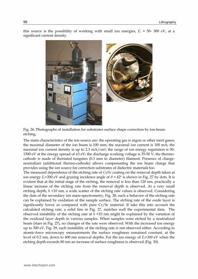
Therefore the application of ion-beam etching at the final correction stage looks very attractive This method allows in particular when focused ion-beams are used to realize the ldquomasklessrdquo correction without frequent opening of the installation to atmosphere Now this method is widely used for substrate form correcting and even for final ion-beam polishing in optical industry (Allen et al 1991 Chason amp Mayer 1993 Ghigo et al 2007) Recently an intensive literature has evolved which is devoted to the application of this method for the precision correction of substrates for projection EUV lithography (Dinger et al 2000 Murakami 2007) For the ion beams applied for the surface shape correction of substrates for EUV and soft X-ray optical elements a number of requirements are imposed the basic of which is the preservation of the surface roughness at an initial (supersmooth) level even when the removed layer depth reaches a few hundreds of nanometers Therefore an optimization of ion energy and incidence angles of the ions on the corrected surface at different depths of material removal is an actual problem Other problems inviting a further investigation are connected with some features of the ion-beam etching at an extremely small depth (asymp 1 nm) removal of materials The experiments have been performed on the installation (Fig 26) with the Cauphmanraquo type ion-beam source KLAN-103M (Website Platar Company 2009) The basic advantage of
wwwintechopencom
Lithography
96
this source is the possibility of working with small ion energies Еi = 50- 300 eV at a significant current density
Fig 26 Photographs of installation for substrates surface shape correction by ion-beam etching
The main characteristics of the ion source are the operating gas is argon or other inert gases the maximal diameter of the ion beam is 100 mm the maximal ion current is 100 mA the maximal ion current density is up to 23 mAcm2 the range of ion energy regulation is 50-1500 eV at the energy spread of plusmn3 eV the discharge working voltage is 35-50 V the thermo-cathode is made of thoriated tungsten (03 mm in diameter) filament Presence of charge-neutralizer (additional thermo-cathode) allows compensating the ion beam charge that provides using the ion source for correction substrates of dielectric materials too The measured dependence of the etching rate of CrSc coating on the removal depth taken at ion energy Еi=200 eV and grazing incidence angle of θ = 42ordm is shown in Fig 27 by dots It is evident that at the initial stage of the etching the removal is less than 120 nm practically a linear increase of the etching rate from the removal depth is observed At a very small etching depth h lt10 nm a wide scatter of the etching rate values is observed Considering the data of the secondary ion mass-spectrometry Fig 28 such a behavior of the etching rate can be explained by oxidation of the sample surface The etching rate of the oxide layer is significantly lower as compared with pure CrSc material If take this into account the calculated etching rate a solid line in Fig 27 matches well the experimental data The observed instability of the etching rate at h lt10 nm might be explained by the variation of the oxidized layer depth in various samples When samples were etched by a neutralized beam (stars in Fig 27) no changes of the rate were observed With the increased ion energy up to 300 eV Fig 29 such instability of the etching rate is not observed either According to atomic-force microscopy measurements the surface roughness remained constant at the level of 02 nm down to 400 nm removal depths For the ion energy of Еi=300 eV when the etching depth exceeds 80 nm an increase of surface roughness is observed (Fig 30)
wwwintechopencom
Manufacturing and Investigating Objective Lens for Ultrahigh Resolution Lithography Facilities
97
Fig 27 Dependence of etching rate on removal depth of CrSc multilayer structures dots are experiment with ions stars are experiment with neutrals and line is calculation accounting etching of the oxidized layer Ion energy Еi = 200 eV and current Ii=60 mA
0 5 10 15 20 25 30 35 40 4500
40x104
80x104
12x105
16x105
Oxigen
SIM
S in
ten
sit
y a
u
Depth nm
Fig 28 Typical distribution of oxygen atoms on depth of CrSc multilayer structure taken by secondary ion mass-spectrometry
The dependences of etching depth on an ion dose (the dose is the product of ion current and etching time) both from the ion current at fixed time and from the time at fixed current show a good linearity that is useful from the practical point of view because it allows to easily define the necessary etching time at a given ion current The example of the dependences of the etching depth on the dose is given in Fig 31 The dashed line corresponds to the linear approximation of the dependence and line with squares represents the experimental data It should be noted that the experiments carried out with greater ion energies up to Ei=15 keV have shown a fast growth of the surface roughness even at small nearby 20ordm grazing angles of incidence of the ions on the surfaces (Chkhalo et al 2008)
wwwintechopencom
Lithography
98
Fig 29 Dependence of ion etching rate on etching depth of CrSc multilayer structures at ion energy Еi = 300 eV (area of small removal depths)
Fig 30 Dependence of surface roughness of CrSc multilayer structures on etching depth at sputtering by argon ions with energy Еi = 300 eV
Fig 31 Dependence of etching depth of the CrSc multilayer structures on ions doze at ion energy Еi = 300 eV - - - linear approximation of the dependence
0 20 40 60 80 1000
10
20
30
40
Etc
hin
g d
ep
th n
m
Dosage mAmin
wwwintechopencom
Manufacturing and Investigating Objective Lens for Ultrahigh Resolution Lithography Facilities
99
For correcting the surface shape of substrates for imaging X-ray optics when the subnanometer form accuracy is required the following strategy providing minimal time expenses has been chosen At the initial stage when peak-to-valley values (P-V) of the surface shape are 50-200 nm the local deposition of the thin films is applied Then at the reduction of the P-V values down to 10-20 nm the ion beams with the energy of 200 eV are used At the final correction stage the 300 eV-ions are applied Figure 32 illustrates the result of using this correction procedure for a spherical substrate with a numerical aperture of NA=025 (the diameter is 130 mm and the curvature radius is 260 mm) which was initially the standard etalon for a conventional interferometer The initial surface map is shown in Fig 32 a) The parameters of the surface were P-V=426 nm and RMS=73 nm The surface shape improved to P-V=73 nm and RMS=06 nm (Fig 32 b)) Thus a root-mean-square deviation of the initial surface shape from an ideal sphere has decreased in 12 times ie in units of the interferometer working wavelength (=0633 microm) it has became better than λ1000 The photograph of this mirror mounted on a metal frame is given in Fig 33
Fig 32 Maps of deviations of the spherical surface shape from the nearest ideal sphere a) initial shape (P-V=426 nm RMS=73 nm) b) after 12-th correction (P-V=73 nm RMS=06 nm)
Fig 33 Photograph of the multilayer spherical mirror for 135 nm wavelength in the frame Diameter of the working aperture is 130 mm
wwwintechopencom
Lithography
100
In spite of a greater wavelength of the traditional deep ultraviolet lithography (193 nm) because of a great number of lens and high requirements for the quality of the projective objectives the methods of correction and certification with a subnanometer accuracy described in this article are urgent for the refracting optics too In connection with this the researches on etching of fused quartz surfaces by ion beams with a compensated charge have been carried out As well as in the case of metal surfaces the main attention was given to the etching rate to the reproducibility of the etching process and to the surface microroughness depending on the beam characteristics incidence angles and material removal depths In Fig 34 the dependences of quartz etching depth on the etching dose are presented The dashed lines in the figure correspond to linear approximations of the dependencies The ion energy was 200 and 300 eV the grazing incidence angle was 42ordm The comparison with similar dependences for CrSc Fig 31 shows that the etching rate of fused quartz is almost twice as much No nonlinearity at the initial stage of the etching is observed that on the one hand proves the hypothesis about the effect of the oxide layer in the case of CrSc material and on the other hand essentially facilitates the correction process
0 100 200 300 4000
50
100
150
200
250
300
350
Etc
hin
g d
ep
th n
m
Dosage mAmin
Fig 34 Dependences of the etching depth on the doze for fused quartz Etching is performed by argon ions with compensated charge and with energy Еi = 200 and 300 eV - - - - linear approximation of dependences
The data on the surface roughness of a fused quartz substrate etched by ions (neutrals) with energies of 200 and 300 eV for various removal depths measured by means of the atomic-force microscope and by x-ray diffractometry are presented in table 1 The substrates manufactured by General optics (USA) were used in the experiment The minimal roughness of initial surfaces measured with an atomic-force microscope was 013 nm and with the x-ray reflection it was about 04 nm From the table it is evident that atomic-force microscope measurements have shown a weaker influence of the etching process on the surface roughness in comparison with the roughness measurements made by the x-ray diffractometry method A more detailed discussion of this difference is beyond the given article Thus the presented experimental data show that these technologies of vacuum deposition and ion-beam etching in the aggregate allow to correct with a subnanometer accuracy the surface shape of optical elements practically of any materials (metals dielectrics semiconductors) with keeping the surface on a supersmooth level This technology is
wwwintechopencom
Manufacturing and Investigating Objective Lens for Ultrahigh Resolution Lithography Facilities
101
suitable for manufacturing elements for imaging x-ray optics and for high resolution systems in visible and deep ultra-violet ranges
Table 1 Roughness of fused quartz substrates depending on neutral (ion) energy and etching depths measured by atomic-force microscopy (AFM) and x-ray diffractometry (X-ray) methods
8 Reflecting multilayer interference mirrors
The final stage of manufacturing a precise mirror for ultrahigh resolution imaging x-ray optical systems is the procedure of the deposition of multilayer reflecting coating on a substrate A low polarizability of materials (le1) and correspondingly a small jump of the refraction factor Δn=00001-01 on the vacuum-material interface and a strong absorption of the radiation by all materials completely exclude the application of refractive optics in the extreme ultra-violet and soft x-ray ranges Because of a low reflection from one interface the reflection optics of normal incidence can be only interferential and the number of layers demanded for the achievement of a high reflectivity depending on a wavelength can reach a value of 102-103 The absorption of the radiation in multilayer structures leads to the fact that the reflectivity is always less than unity While choosing an optimal pair of materials providing a maximal reflectivity on a given wavelength the circumstance is often used that in the range of wavelengths directly adjoining the absorption edge of the material gt AE (AE is the wavelength of the material absorption edge) and coinciding with an anomalous dispersion of the optical constants the lowest absorption and the maximal polarizability of materials are observed For some materials in the field of K-and L- absorption edges the refraction factor can even exceed unity In Fig 35 the calculated spectral dependences of the maximal reflection coefficients for the most attractive pairs of materials in a spectral range of 3 - 16 nm representing the biggest interest for projection nanolithography and high resolution x-ray microscopy are shown The greatest experimental reflectivity about 70 was obtained at a wavelength of 135 nm The spectral range around λasymp67 nm (area of boron anomalous dispersion) is of interest for projection x-ray lithography However the reflectivity obtained here with LaB4C multilayer mirrors at a normal angle of incidence does not exceed 45-47 (Andreev et al 2009) that is not enough for lithographic applications
wwwintechopencom
Lithography
102
2 3 4 5 6 7 8 9 10 11 12 13 14 15 1600
01
02
03
04
05
06
07
08
CrSc
CrC
LaB
MoBe
MoSi
experiment
Refle
ctivity
Wavelength nm
Fig 35 Calculated (lines with symbols) and experimental (stars (Website ESRF 2006 Andreev et al 2003)) reflection coefficients of mostly attractive pairs of materials in X-ray and EUV ranges
On the short-wave length side the working wavelength of the normal incidence multilayer optics is limited by technology capabilities for depositing high-quality short period multilayer structures At present the shortest periods have multilayer structures based on WB4C (the period dasymp1 nm) (Vainer et al 2006 Platonov 2002) and CrSc (dasymp15 nm) (Salashchenko amp Shamov 1997 Website ESRF 2006) A number of special requirements are imposed on the multilayers which should be deposited onto substrates for imaging optics In particular to provide a constructive interference of the waves reflected from different interfaces the radiation wavelength λ the local angle of incidence ( )rθ f
and the period of the multilayer structure ( )d rf should satisfy
the Bragg condition
( )2sin ( )
d rr
λθ=f
f (11)
where rf is a radius-vector of a point of incidence of the radiation on the structure As the
incidence angles are a function of the coordinates it results in the necessity to deposit multilayer structures with a variable over the surface period so-called ldquogradedrdquo structures In some cases for example when the angular divergence of the X-ray beam falling on one point of the mirror surface exceeds the Braggrsquos peak width the multilayer structure should have a variable period on depth (Kozhevnikov et al 2001) One more important feature of multilayer structures for precise optics can be explained as follows For multilayer dispersive elements the maximum deviation of the local value of the period d from the nominal one is determined by the condition of synchronism of the waves reflected from various interfaces which can be expressed through the spectral selectivity of a mirror 1 S d d Nδλ λ δ= = cong (N is a number of periods) In the case of precision multilayer imaging optics when the required surface shape accuracy is at a subnanometer
wwwintechopencom
Manufacturing and Investigating Objective Lens for Ultrahigh Resolution Lithography Facilities
103
level to the synchronism condition an extra requirement for the preservation of the mirror surface shape is added For example for the well-known MoSi multilayer structure optimized on the wavelength of λ=135 nm the period is dasymp7 nm at a number of periods N asymp 40 Correspondingly the general thickness of the structure is L=Nd=280 nm The local error of the period of 1 will affect weakly on reflectivity however the surface shape of the mirror will produce a change of 28 nm which already can essentially produce an influence on imaging properties of the mirror From these simple estimations two important conclusions follow Firstly when designing and manufacturing the surface shape of a substrate it is necessary to take into account the real thickness of a multilayer coating which would be deposited onto the substrate Secondly it is necessary to provide a high at a level of 02-03 accuracy of local values of the period over the mirror surface Besides an intrinsic stress in the multilayer structures which can also deform the surface shape must be taken into account The estimation of the deformation x of a substrate with a diameter D a thickness hsub with the Yung modulus E and the Poisson factor ν on which a hf thick film with the intrinsic stress σ is deposited can be performed by means of equations
2
2
3
4
1
f
sub
h Dx
Y h
EY
σδ
ν
sdot sdot= sdotsdot= minus
(12)
For instance for optimized on maximum of the reflection coefficient MoSi multilayer structure (portion of Mo layer in the period =dMo(dMo+dSi) = 04) the stress in our case is about σ =-350 М『а (Fig 36) At deposition of such a multilayer structure (general thickness is L=Nd=280 nm) on a substrate of fused quartz with the diameter D=220 mm and thickness h=50 mm (Y=844 》а) the maximal deformation of the substrate surface would be about 17 nm that essentially exceeds an admissible level of the surface shape deformation of a mirror for EUV lithography Different groups solve this problem in different ways One the solution is the use of mirrors with a specified thickness ratio of molybdenum layer in the periods Mo asymp 05 - 07 when the stress is close to zero (Windt et al 1994 Zoethout et al 2003) The other solution consists in adding a third material into the periods for example Ru (Oshino et al 2003) However all these methods either because of a stronger absorption of EUV radiation or because of an interface roughness growth have smaller of 10-20 absolute values of the reflectivity In IPM RAS a technique of the stress compensation based on the use of special sublayers lying under the basic MoSi multilayer structure is under development For CrSc multilayer structures the stress is close to zero at γCr=dCr(dCr+dSc)asymp05 (Fig 37 (Andreev et al 2005)) At γCrgt05 a sign of the stress is positive on the contrary to the MoSi structures at γMo= 04 when it is negative The total stress σeff in the structure consisting of CrSc and MoSi multilayer films can be determined from a ratio
( ) ( )
( ) ( )Mo Si Mo Si Mo Si Cr Sc Cr Sc Cr Sc
eff
Mo Si Mo Si Cr Sc Cr Sc
d N d N
d N d N
σ σσ ⎡ ⎤sdot sdot + sdot sdot⎣ ⎦= sdot + sdot (13)
from which it follows that optimizing the composition and the thickness of CrSc layers it is possible to compensate the stress in the basic MoSi reflecting multilayer structure
wwwintechopencom
Lithography
104
Fig 36 Stress in MoSi multilayer structures depending on ratio of Mo layer in period γMo=dMo(dMo+dSi) at fixed period d=697 nm
Fig 37 Stress in CrSc multilayer structure depending on ratio of Cr layer in period γCr=dCr(dCr+dSc) at fixed period d=54 nm
In practice it is necessary to consider a process of the stress relaxation which depending on the structure and materials is variable over several days Totally the stress can change by tens percent An example of such a process is illustrated in Fig 38 in which the time dependencies of the stress in multilayer structures consisting of anti-stress CrSc sublayers and MoSi reflecting layers are presented The structures differ by thicknesses of the sublayers It is necessary to note that the stress value is affected not only by ratio of the layer thickness in the period but also by the period size and conditions in which the films were deposited For depositing multilayer structures a method of magnetron spattering is used in IPM RAS The method allows depositing films onto curved as well as flat substrates The conditions under which multilayer structures are deposited are briefly described in section 6 devoted to the correction of the substrate surface shape by the method of local thin-film deposition The facilities have from two to six magnetron sources that allows depositing at one technological cycle reflecting anti-stress and anti-diffusion barrier layers Now the
σ MP
a
-1000
-800
-600
-400
-200
0
200
400
600
02 04 06 08 10
γMo=dMo (dMo+dSi)
0
100
200
300
400
500
600
700
06 065 07 075
σ MP
a
γCr = dCr (dCr+dSc)
wwwintechopencom
Manufacturing and Investigating Objective Lens for Ultrahigh Resolution Lithography Facilities
105
technologies of depositing more than twenty various pairs of materials are developed It allows manufacturing optics for a whole x-ray and extreme ultra-violet spectral range More details about the properties of the multilayer structures can be found in (Andreev et al 2003)
Fig 38 Stress in MoSi multilayer structures with anti-stress CrSc sublayers versus of time a) - [(CrSc)times42 d=538 nm =067 (MoSi))times45 d=698 nm =04] and b) - [(CrSc)times40 d=538 nm =067 (MoSi)times45 d=698 nm =04]
A great volume of works high requirements for the coating quality and for accuracy of the period distribution over a substrate surface dictate the need for an operative information about characteristics of the deposited coatings with the purpose of correcting the technological process It is most convenient to perform such work with the presence of laboratory reflectometers allowing the investigation of multilayer structures on working wavelengths and located in the immediate vicinity of technologists Therefore laboratory reflectometers are constantly being developed and improved recently In Refs (Loyen et al 2003 Miyake et al 2003 Gulikson et al 1992) the specialized reflectometers for investigating multilayer optics in the range around 135 nm are described As a source of the soft x-ray and EUV radiation the laser plasma is used which arises due to the irradiation of solid-state targets by laser light with a power density about 109 Wcm2 For monochromatization the radiation spherical diffraction gratings operating at grazing angles are used The characteristic fluxes of the photons in the working range of wavelengths of 10-16 nm on the investigated samples with the probe beam size asymp 2 mm are 107 - 108 photons (01 nmtimess) The results of reflectivity measurements of MoSi multilayer mirrors in the area of 135 nm obtained with the help of these reflectometers as compared with the data obtained with a PTB-reflectometer (synchrotron BESSY-2 Berlin Germany which is considered as the reference one) have shown the coincidence of the measured reflection coefficients at a level of 3 and the resonant wavelength asymp 001 nm The basic disadvantages of these reflectometers in our opinion are a narrow range of working wavelengths and a low spectral resolution caused by the applied monochromator scheme The monochromator consists of two stationary slits and spherical (or toroidal) diffraction grating Scanning across the spectrum is carried out due to the diffraction gratings rotation around its axis According to this arrangement the position of the slits and the diffraction grating coincides with the Rowland circle (Rowland 1893) only for one
-30
-20
-10
0
10
20
30
50 100 15 200 250
Time hours
σ eff
MP
a
a)
t days
σ MPa
- 40
- 30
- 20
- 10
0
1 2 3 4 5 6 7 8 9
x
x
xx
x x
b)
wwwintechopencom
Lithography
106
wavelength that essentially limits the range where the spectral resolution of the monochromator is kept at the acceptable level of Δλapp asymp 001-002 nm The other factor limiting working spectral range of the reflectometer is the type of the used radiation source (laser plasma) which large size does not allow scanning by the entrance slit of the grating spectrometer Our group develops multilayer optics for a wide spectral range λ=06-50 nm and the monochromator spectral resolution up to 0003-0005 nm is frequently required Therefore in IPM RAS laboratory reflectometers on the basis of high resolution grating monochromators have been developed These monochromators have a movable entrance slit and diffraction grating (Chkhalo et al 1998 Zuev amp Mitrofanov 2002 Bibishkin et al 2004 Bibishkin et al 2005) In the reflectometrs the monochromators of type RSM-500 (Lukirsky et al 1967) and McPherson-247 (Website Mcpherson Company 2009) are used The photograph and optical scheme of the last generation reflectometer are given in Fig 39 Owing to such a spectrometer the kinematic scheme slits and diffraction grating are always located in the Rowland focusing circle so that the high spectral resolution of the device in the whole range of wavelengths is provided Two diffraction gratings with various radiuses of curvature cover this spectral range
Fig 39 Optical scheme and photograph of the reflectometer XRT - x-ray tube S1 S2 - entrance and exit slits AS VS - horizontal and vertical anti-scattering slits DG - diffraction grating TM - toroidal mirror M ndash probe beam intensity monitor MIS - investigated sample D ndash detector G5 ndash five-axes goniometer
In the reflectometer the radiation from the anode of the x-ray tube (XRT) through the entrance slit of the monochromator (S1) falls on the diffraction grating (DG) The diffracted monochromatic radiation according to the diffraction grating equation cosϕ - cosψ =mλD (m - the order of diffraction λ ndash a wavelength and D - the grating period ϕ and ψ angles of diffraction and incidence correspondingly) is focused onto the spectrometer exit slit S2 Scanning across the spectrum is carried out by linear moving of the diffraction grating and the exit slit with a simultaneous turn of the diffraction grating so that the condition Xl=Rgsdot sinψ where Rg - radius and Xl - distance between the diffraction grating center and the exit slit is satisfied An anti-scattering diaphragm (AS) reduces the intensity of scattered radiation at the output of the monochromator and limits the irradiated area of the diffraction grazing The monochromatic radiation by means of a toroidal mirror (TM) is focused on the investigated sample The other important function of the toroidal mirror is connected with a filtration of higher diffraction orders which is especially urgent when
wwwintechopencom
Manufacturing and Investigating Objective Lens for Ultrahigh Resolution Lithography Facilities
107
working with bremsstrahlung of the tungsten anode Radiuses of the toroidal mirror are chosen in such a way that in a horizontal plane the exit slit and in a vertical plane the source are imaged on the sample under study The studied sample is installed on a five-axis goniometer which photograph and scheme of movements are shown in Fig 40 The linear translation along X and Z axes the rotation around them (ω and ) and the inclination θ allow to insert any point of the sample under study with a diameter up to 300 mm into the x-ray beam The detector executes 2 rotation The additional inclination of the detector 2θ allows to increase the numerical aperture of the sample which can be tested up to NA=05
Fig 40 Photograph of the goniometer and scheme of movements provided by the goniometer
The concept of a spectrometer-monochromator with a movable slit and diffraction grating became possible only due to the application of the dismountable x-ray tube of an original design as the radiation source The advantages of classical sealed x-ray tubes are their small dimensions and weight simplicity in operation sufficient for reflectometric applications intensity of the x-ray radiation and long life-time However the application of these sources for precision reflectometry in soft x-ray and extreme ultra-violet ranges has shown that because of the fast contamination of the anode by products of thermocathode material erosion and hydrocarbons decomposition under a powerful electron-beam emission characteristics and life-time of the tubes collapsed when comparing with expected values For solving this problem in our work the tube was equipped with an ion-beam source for cleaning anodes from contaminations (Bibishkin et al 2003) It allows to work without opening the spectrometer and the tube to the atmosphere within several months thus approaching its operation mode to the traditional sealed X-ray tubes for hard X-rays The work is done on K L and M characteristic lines of target (anode) materials and on continuous bremsstrahlung spectrum of tungsten On one holder about 8 targets of various materials are installed It is necessary to note that frequently it is possible to use a few spectral lines from one target
wwwintechopencom
Lithography
108
As an illustration in Fig 41 the measured spectral dependence of reflectivity of MoSi multilayer spherical mirror shown in Fig 40 is presented The measurement has been performed with the reflectometer at an incidence angle of the radiation to the sample of 5ordm (from the local normal)
Fig 41 Spectral dependence of the reflection coefficient of MoSi multilayer mirror deposited onto spherical substrate Angle of incidence was 5ordm from the local normal
One more important advantage of the x-ray tube as a source of X-ray radiation is that in the field of wavelengths lt3 nm because of aberrations of spherical grating the spectral width of the probe beam is ΔGge 001 nm while the spectral resolution of short period multilayers reaches values Δ MIS lt001 nm Since the natural width of characteristic lines of some materials in this range is essentially less than this value this circumstance provides precision measurements of reflective characteristics of multilayer mirrors even when monochromator does not provide the demanded resolution Thus the developed in IPM RAS methods of multilayer coating deposition stress compensation in the film structures laboratory metrology of the mirrors at working wavelengths restoration of the substrates without any damage of the substrate surface shape and roughness allow us to make and certify high reflecting multilayer mirrors with a sub-nanometer level surface shape accuracy attended for super-high resolution imaging X-ray optics
9 Conclusion
In the given article the basic researches and the full cycle of developed in IPM RAS technologies and metrology techniques from the substrate surface shape correction to the deposition of multilayer coatings on them which are required for manufacturing high reflecting mirrors for diffraction quality imaging in the extreme ultra-violet and in the soft X-ray ranges are described As a whole it is evident that the problem of manufacturing such optics for high resolution EUV lithography and X-ray microscopy is already solved as a first approximation The further activity should be directed toward the increase of both in manufacturing accuracy of optical surfaces up to a level of RMS=01 nm and in the numerical aperture of objectives up to NA=04-06
0
10
20
30
40
50
60
70
126 130 134 138 142
Wavelength nm
Refl
ect
ivit
y
wwwintechopencom
Manufacturing and Investigating Objective Lens for Ultrahigh Resolution Lithography Facilities
109
In this connection upgrading the interferometric methods for surface shape measurements of optical elements and wave-front deformations of objectives first of all and regarding the increase of their working numerical aperture is a subject of current interest The diffraction interferometers utilizing the tipped fiber as a source of the reference spherical wave look rather attractive Owing to the simplicity of the design high intensity of the diffracted wave weak sensitivity to the adjustment in an optical circuit and a number of other advantages the interferometers which are simple in operation can be developed for the optical industry In the framework of the given article the problem arising when aspherical surfaces are under investigation of development and optimization of correctors transforming the reference spherical fronts into the aspherical ones which shapes are identical to the shapes of the studied surfaces was not practically discussed Meanwhile traditional lens null-correctors have limited capabilities rather complicated in manufacturing and expensive and demand complicated calibrating procedures for taking into account the wave-front distortions due to errors of the corrector itself In this connection diffraction correctors represent a significant interest (Akatov et al 2004) A gross potential for the surface shape correction of dielectric materials by means of ion-beams has RF-etching in chemically active environments The first experiments on etching of quartz substrates by means of the RF-etching have shown that the surface micro-roughness did not change down to the removal depths of a few micrometers (Akhsakhalyan et al 2008) The most serious problem on the way of manufacturing the effective optics for the soft X-ray radiation λlt10 nm is that reflection coefficients of the multiplayer mirrors are not sufficiently high Nevertheless the results that have been recently obtained in the field of the X-ray optics teams may be considered as a break-through because they lay the foundation of developing such important physico-technological directions as projection EUV nanolithography X-ray microscopy and extraterrestrial astronomy of the ultrahigh resolution
10 References
Akhsakhalyan AD Vainer YuA Volgunov DG Drozdov MN Kluenkov EB Kuznetcov MI Salashchenko NN Kharitonov AI amp Chkhalo NI (2008) Application of reactive ion-beam etching for surface shape correction of X-ray mirrors Proceedings of Workshop ldquoX-ray optics ndash 2008rdquo pp 26-28 Chernogolovka Moscow region 6-9 October 2008 p 26-28 IPTM Chernogolovka (in Russian)
Allen LN Keim RE amp Lewis TS (1991) Surface error correction of a Keck 10 m telescope primary mirror segment by ion figuring Proceedings SPIE Vol 1531 1991 pp 195ndash204
Andreev SS Bulgakova SA Gaponov SV Gusev SA Zuev SYu Kluenkov EB Luchin VI Lopatin AYa Mazanova LM Prokhorov KA Sadova EN Salashchenko NN amp Shamov EA (2000) Investigations in field of projection lithography of extreme ultraviolet region in Institute for physics of microstructures RAS Surface X-ray synchrotron and neutron investigations Vol 1 2000 pp 32-41 (in Russian)
Andreev SS Akhsakhalyan AD Bibishkin MS Chkhalo NI Gaponov SV Gusev SA Kluenkov EB Prokhorov KA Salashchenko NN Schafers F amp Zuev
wwwintechopencom
Lithography
110
SYu (2003) Multilayer optics for XUV spectral region technology fabrication and applications Central European Journal of Physics Vol 1 2003 pp 191-209
Adreev SS Kluenkov EB Misinov AL Polkovnikov VN Salashchenko NN Suslov LA amp Chernov VV (2005) Compensation of elastic deformation of MoSi multilayer structures on quartz and zerodur substrates using buffer CrSc technique Surface investigations Vol 2 2005 pp 45-48 (In Russian)
Andreev SS Barysheva MM Chkhalo NI Gusev SA Pestov AE Polkovnikov VN Salashchenko NN Shmaenok L A Vainer YuA amp Zuev SYu (2009) Multilayered mirrors based on LaB4C(B9C) for x-ray range near anomalous dispersion of boron ( near 67 nm) Nuclear Instruments and Methods in Physics Research SecA Vol 603 2009 pp 80-82
Archer KM (1997) Craniofacial reconstruction using hierarchical b-spline interpolationrdquo A thesis submitted in partial fulfilment of the reguirements for the degree of master of applied science The university of British Columbia 1997 p 113
Asadchikov VE Kapabekov AYu Kozhevnikov IV Levashov VE amp Sagitov SI (1998) Experimental investigation of roughness correlation of a film and a substrate by means of X-ray scattering Crystallography Vol 43 No 1 1998 pp 119-130 (In Russian)
Barbee TW (Jr) (1981) Sputtered layered synthetic microstructures (LSM) dispersion elements Proceedings of Conference ldquoLow energy X-ray diagnosticsrdquo pp 131-145 Monterey USA 1981 N Y Amer Inst Phys
Benschop JPH Kaiser WM amp Ockwell DC (1999) EUCLIDES the European EUVL program SPIE Symposium on Micro-lithography Vol 3676 1999 p 246
Bibishkina MS Zabrodin IG Klyuenkov EB Salashchenko NN Chekhonadskih DP amp Chkhalo NI (2003) A new dismountable tube for soft X-ray radiation Surface investigations No 2 2003 pp 41-45 (In Russian)
Bibishkinb MS Zuev SYu Salashchenko NN amp Chkhalo NI (2003) Measuring of microroughness of surfaces using soft X-ray radiation Surface investigations No 1 2003 pp 94-96 (In Russian)
Bibishkin MS Chekhonadskih DP Chkhalo NI Klyuenkov EB Pestov AE Salashchenko NN Shmaenok LA Zabrodin IG amp Zuev SYu (2004) Laboratory methods for investigation of multilayer mirrors in Extreme Ultraviolet and Soft X-Ray region Proceedings of SPIE Vol 5401 2004 pp 8-15
Bibishkin MS Vainer YuA Pestov AE Prokhorov KA Salashchenko NN Fraerman AA amp Chkhalo NI (2005) Investigation of characteristics of multilayer X-ray mirrors with ultra-short periods d = 07-24 せす Bulletin of the Russian Academy of Sciences Physics Vol 69 No 2 2005 pp 199-206
Blunt R (2006) White light interferometry - a production worthy technique for measuring surface roughness on semiconductor wafers Proceedings of CEMANTECH Conference pp 59-62 Vancouver Canada April 24-27 2006
Born M amp Wolf E (1973) Principles of optics second edition Science Moscow (In Russian)
Braat J (1987) Polynomial expansion of severely aberrated wave fronts Optical Society of America Vol 4 No 4 1987 pp 643-650
Chason E amp Mayer T M (1993) Low energy ion bombardment induced roughening and smoothing of Si02 surfaces Applied Physics Letters Vol 62 No 4 1993 pp 363-365
Cheng P (1987) Instrumentation and Biological Applications In X-ray Microscopy Springer Verlag
wwwintechopencom
Manufacturing and Investigating Objective Lens for Ultrahigh Resolution Lithography Facilities
111
Chkhalo NI Dolbnya IG Fedorchenko MV Kruglyakov EP Zarodyshev AV amp Zolotarev KV (1993) Multilayer mirror on copper-nickel substrates for intense X-ray beams Proceedings of the 4-th International Conference ldquoX-Ray Microscopy 4rdquo pp 586-592 Russia Chernogolovka September 20-24 1993 IPTM Chernogolovka
Chkhalo NI Fedorchenko MV Kruglyakov EP Volokhov AI Baraboshkin KS Komarov VF Kostyakov SI amp Petrov EA (1995) Ultradispersed diamond powders of detonation nature for polishing X-ray mirrors Nuclear Instruments and Methods in Physics Research A Vol 359 1995 pp 155-156
Chkhalo NI Kirpotin AN Kruglyakov EP amp Semenov EP (1998) Reflectometer for precision tests of optical components in the ultrasoft X-ray range Nuclear Instruments and Methods in Physics Research A Vol 405 1998 pp 393-395
Chkhaloa NI Raskin DG amp Salashchenko NN (2008) Capabilities of microinterferometer with digital recording of images for studying micro-objects with sub-nanometer resolution Proceedings of SPIE Vol 7025 2008 p 702512
Chkhalob NI Dorofeyev IA Salashchenko NN amp Toropov MN (2008) A plane wave diffraction on a pin-hole in a film with a finite thickness and real electrodynamic properties Proceedings of SPIE Vol 7025 2008 p 702506
Chkhaloc NI Klimov AYu Rogov VV Salashchenko NN amp Toropov MN (2008) A source of a reference spherical wave based on a single mode optical fiber with a narrowed exit aperture Rev Sci Instrum Vol 79 2008 p 033107
Chkhalod N Paramonov L Pestov A Raskin D amp Salashchenko N (2008) Correction of the EUV mirror substrate shape by ion beam Proceedings of SPIE Vol 7025 2008 p 702503
Dinger U Bisert F Lasser H Mayer M Seifert A Seitz G Stacklies S Stickel F-J amp Weise M (2000) Mirror substrates for EUV-lithography progress in metrology and optical fabrication technology Proceedings of SPIE Vol 4146 2000 pp 35ndash46
Dorofeyev I Jersch J amp Fuchs H (2003) Spectral composition of electromagnetic fluctuations induced by a lossy layered system Annalen der Physik Vol 12 No 7-8 2003 pp 421-437
Dorofeev I (2009) Amplitude-phase characteristics of electromagnetic fields diffracted by a hole in a thin film with realistic optical properties Physica E Vol 41 2009 pp 762-770
Drozdov MN Drozdov YuN Barysheva MM Polkovnikov VN amp Chkhalo NI (2009) Minimization of matrix effects upon layer-by-layer analysis of multilayer metallic nanostructures LaB4C by SIMS using cluster secondary ions Proceedings of Symposium ldquoNanophysics and nanoelectronicsrdquo Vol 1 pp 190-191 Nizhniy Novgorod Russia 16-20 March 2009 IPM RAS Nizhniy Novgorod (in Russian)
Gavrilin DA (2003) Investigations of methods for shape description of complicated optical surfaces at interferometrical control PhD thesis St-Petersburg Russia 103 p (in Russian)
Ghigo M Canestrari R Spiga D amp Novi A (2007) Correction of high spatial frequency errors on optical surfaces by means of Ion Beam Figuring Proceedings of SPIE Vol 6671 2007 p 667114
Goldberg KA amp Kevin G (2001) Wave-front measurement errors from restricted concentric subdomains J Opt Soc Am A Vol 18 No 9 2001 pp
wwwintechopencom
Lithography
112
Goldberg KA Naulleau P Bokor J Chapman HN amp Barty A (2002) Testing extreme ultraviolet optics with visible-light and extreme ultraviolet interferometry J Vac Sci Technol B Vol 20 No 6 2002 pp 2834-2839
Griffith J E amp Grigg DA (1993) Dimensional metrology with scanning probe microscopes Journal of Applied Physics Vol 74 1993 pp R83-R109
Gullikson EM Underwood JH Batson PC and Nikitin V (1992) A soft X-rayEUV reflectometer based on a laser produced plasma source Journal of x-ray science and technology Vol 3 1992 pp 283-299
Gwyn C (1998) White paper on Extreme ultraviolet Lithography Proceedings of EUV LLC 1998 Livermore
Klimov AYu Rogov VV Salashchenko NN amp Chkhalo NI (2008) A Spherical Wave Source Based on a Probe for a Near-Field Microscope Bulletin of the Russian Academy of Sciences Physics Vol 72 No 2 2008 pp 204-206
Kluyenkova EB Pestov AE Polkovnikov VN Raskin DG Toropov MN Salashchenko NN amp Chkhalo NI (2008) Testing and Correction of Optical Elements with Subnanometer Precision Nanotechnologies in Russia Vol 3 Nos 9-10 2008 pp 602-610
Klyuenkovb EB Polkovnikov VN Salashchenko NN amp Chkhalo NI (2008) Shape Correction of Optical Surfaces with Subnanometer Precision Problems Status and Prospects Bulletin of the Russian Academy of Sciences Physics Vol 72 No 2 2008 pp 188-191
Kozhevnikov IV Asadchikov VE Duparre A Gilev ON Havronin NA Krivonosov YuS Ostashev VI amp Steinert J (1999) Comparative study of the roughness of optical surfaces and thin films using atomic force microscopy x-ray scattering and light scattering methods Proceedings of SPIE Vol 3739 1999 pp 348-354
Kozhevnikov IV Bukreeva IN amp Ziegler E (2001) Nuclear Instruments and Methods in Physics Research Sec A Vol 460 2001 p 424
Linnik VP (1933) A simple interferometer to test optical systems Bulletin of the Academy of Science of the USSR Vol 1 1933 pp 210-212
Loyen L Bottger T Braun S Mai H Leson A Scholze F Tummler J Ulm G Legall H Nickels PV Sandner W Stiel H Rempel C Schulze M Brutscher J Macco F amp Mullender S (2003) A New Laboratory EUV Reflectometer for Large Optics using a Laser Plasma Source Proceedings of SPIE Vol 5038 2003 pp 12-21
Lukirsky AP Brytov IA amp Komyak NI (1967) Prototype of an X-ray spectrometer with diffraction grating and ionization detection for spectral region of 10-55 Aring Apparatus and methods of X-ray analysis No 2 1967 pp 4-19 L Engineering (in Russian)
Malacara D ed (1992) Optical shop testing 2nd ed John Wiley amp Sons Inc ISBN 0-471-52232-5 New York
Medecki H Tejnil E Goldberg KA amp Bokor J (1996) Phase-shifting point diffraction interferometer Optics letters Vol 21 No 19 1996 pp 1526-1528
Miyake A Miyachi T Amemiya M Hasegawa T Ogushi N Yamamoto T Masaki F amp Watanabe Y (2003) LPP-based reflectometer for characterization of EUV lithography systems Proceedings of SPIE Vol 5037 2003 pp 647-655
Murakami K Saito Y Ota K et al (2003) Development of an experimental EUV interferometer for benchmarking several EUV wavefront metrology schemes Proceedings of SPIE Vol 5037 2003 pp 75-82
wwwintechopencom
Manufacturing and Investigating Objective Lens for Ultrahigh Resolution Lithography Facilities
113
Murakami K Oshino T Kondo H Chiba H Komatsuda H Nomura K amp Iwata H (2007) Development of optics for EUV lithography tools Proceedings of SPIE Vol 6517 2007 pp 65170J
Naulleau PP Goldberg KA Lee SH Chang C Attwood D amp Bokor J (1999) Extreme-ultraviolet phase-shifting point-diffraction interferometer a wave-front metrology tool with subangstrom reference-wave accuracy Appl Opt Vol 38 No 35 1999 pp 7252-7263
Naulleau P Goldberg KA Lee SH Chang Ch Atwood D amp Bokor J (2000) The EUV phase-shifting point diffraction interferometer Synchrotron Radiation Instrumentation Eleventh US National Conference ed by P Pianetta p 66-72 ISBN 1-56396-941-6 American Institute of Physics
Naulleau P Golberg KA Anderson EH et al (2002) Sub-70 nm Extreme Ultraviolet Lithography at the Advanced Light Source Static Microfield Exposure Station Using the Engineering Test Stand Set-2 Optic Jour Vac Sci Technol B Vol 20 2002 pp 2829ndash2833
Nevot L amp Croce P (1980) Characterisation des surfaces par reflection rasante de rayon Application a lrsquoetude du polissage de quelque verres silicates Revue de Physique Appliquee Vol 15 1980 pp 761-779
Okatov MA Antonov EA Baigozhin A et al (2004) Handbook for optical-technologist St- Petersburg Politechnica 2004 679 p
Oshino T Shiraishi M Kandaka N Sugisaki K Kondo H Ota K Mashima K Murakami K Oizumi H Nishiyama I amp Okazaki S (2003) Development of illumination optics and projection optics for high-NA EUV exposure tool (HiNA) Proceedings of SPIE Vol 5037 2003 pp 75-82
Ota K Murakami K Kondo H Oshino T Sugisaki K amp Komatsuda H (2001) Feasibility study of EUV scanners Proceedings of SPIE Vol 4343 2001 pp 60-69
Otaki K Ota K Nishiyama I Yamamoto T Fukuda Y amp Okazaki S (2002) Development of the point diffraction interferometer for extreme ultraviolet lithography Design fabrication and evaluation J Vac Sci Technol B Vol 20 No 6 2002 pp 2449-2458
Palik ED (1985) Hanbook of optical constants of solids Naval Research Laboratory Washington DC 1985 749 pp
Parratt LG (1954) Surface studies of solids by total reflection of x-rays Physical Review Vol 35 1954 pp 359-369
Platonov Yu Gomez L amp Broadway D (2002) Proceedings of SPIE Vol 4782 2002 p 152 Protopopov VV Valiyev KA amp Imamov RM (1999) Measurement of spatial
distribution of superpolished surface roughness and defects in multilayer X-ray mirrors Surface investigations No 1 1999 pp 111-119 (In Russian)
Puryaev DT (1976) Methods for control of aspherical surfaces M Engineering 1976 13 p (in Russian)
Rodionov SA Przhevalinsky LI amp Shekhonin AA (1974) Application of coefficients of interpolation polynomial for optical system aberrations presentation Bulletin of the USSR institutions of higher education Instrument engineering Vol 17 No 10 1974 p 104 (in Russian)
Rodionov SA (1995) Mthematical apparatus for ptics control ndash general approach Optical journal No 8 1995 pp 49-51
Rowland H (1893) Gratings in theory and practice Phil Mag Vol 35 1893 p 397 Salashchenko NN amp Shamov EA (1997) Optics communication Vol 134 1997 p 7
wwwintechopencom
Lithography
114
Salashchenko NN (2001) Optical Element and Method for Recovering the Substrate Patent DE 101 01 820 A1 00074P
Sinha SK Sirota EB Garoff S amp Stanley HB (1988) X-ray and neutron scattering from rough surfaces Physical Rev B Vol 38 No4 1988 pp 2297-2311
Sommargren GE (1996) Diffraction methods raise interferometer accuracy Laser Focus World Vol 8 1996 p 61-71
Soufli R Spiller E Schmidt MA Davidson JC Grabner RF Gullikson EM Kaufmann BB Mrowka S Baker SL Chapman HN Hudyma RM Taylor JS Walton ChC Montcalm C amp Folta JA (2001) Multilayer optics for an extreme ultraviolet lithography tool with 70 nm resolution Proceedings of SPIE Vol 4343 2001 pp 51-59
Stone VW Jonas AM Nysten B amp Legras R (1999) Roughness of free surfaces of bulk amorphous polymers as studied by x-ray surface scattering and atomic force microscopy Physical Rev B Vol 60 No 8 1999 pp 5883-5894
Sun X Chen S amp Shen Q (1998) Geometric calibration of lens using B-spline surface fitting Wuhan University Journal of Natural Sciences Vol 3 No 4 1998 pp 440-442
Swantner W amp Weng W C (1994) Gram-Schmidt orthogonalisation of Zernike polynomials for general aperture shapes Applied optics Vol 33 No 10 1994 pp 1832-1837
Sweeney DW Hudyma RM Chapman HN amp Shafer D (1998) EUV optical design for a 100 nm CD imaging system Proceedings of SPIE Vol 3331 1998 pp 2-10
Underwood JH amp Barbee (Jr) TW (1981) Layered synthetic microstructures as Bragg diffractors for X-rays and extreme ultraviolet theory and predicted performance Appl Opt Vol 20 1981 pp 3027-3034
Vainer YuA Pestov AE Prokhorov KA Salashchenko NN Fraerman AA Chernov VV amp Chkhalo NI (2006) Analysis of Cross-Correlation of Interface Roughness in Multilayer Structures with Ultrashort Periods Journal of Experimental and Theoretical Physics Vol 103 No 3 2006 pp 346-353
Warburton WK Rek ZU amp Barbee (Jr) TW (1987) Quality Investigation of multilayer covers for X-ray optics In X-ray optics and microscopy pp 222-231 World Moscow (In Russian)
Website ESRF httpwwwesrfeueventsconferencespast-conferences-and-workshops pxrms06Detailed-programm12_gulliksonpdf
Website GO Corporation httpwwwgoochandhousegocomproductscat3 Website Mcpherson Company httpwwwmcphersoninccomspectrometers
xuhvvuvuvxuhvvuvuvhtm Website Platar Company httpwwworcru~platarP1Rhtml Website Veeco Instruments httpwwwveecocom Website Zygo Corporation httpwwwzygocom Williamson DM (1995) The elusive diffraction limit OSA Proceedings on Extreme
Ultraviolet Lithography F Zernike and DT Attwood eds Vol 23 1995 pp 68-76 Windt DL Brown WL Volkert CA amp Waskiewicz WK (1994) J Appl Phys Vol 78
1994 p 2423 Zoethout E Sipos G van de Kruijs RWE Yakshin AE Louis E Mullender S amp
Bijkerk F (2003) Stress mitigation in MoSi multilayers for EUV lithography Proceedings of SPIE Vol 5037 2003 pp 872ndash878
Zuev SYu amp Mitrofanov AV (2002) Measurements of parameters of optical elements for X-ray telescopes Surface investigations No 1 2002 pp 81-83 (In Russian)
wwwintechopencom
LithographyEdited by Michael Wang
ISBN 978-953-307-064-3Hard cover 656 pagesPublisher InTechPublished online 01 February 2010Published in print edition February 2010
InTech EuropeUniversity Campus STeP Ri Slavka Krautzeka 83A 51000 Rijeka Croatia Phone +385 (51) 770 447 Fax +385 (51) 686 166wwwintechopencom
InTech ChinaUnit 405 Office Block Hotel Equatorial Shanghai No65 Yan An Road (West) Shanghai 200040 China
Phone +86-21-62489820 Fax +86-21-62489821
Lithography the fundamental fabrication process of semiconductor devices plays a critical role in micro- andnano-fabrications and the revolution in high density integrated circuits This book is the result of inspirationsand contributions from many researchers worldwide Although the inclusion of the book chapters may not be acomplete representation of all lithographic arts it does represent a good collection of contributions in this fieldWe hope readers will enjoy reading the book as much as we have enjoyed bringing it together We would liketo thank all contributors and authors of this book
How to referenceIn order to correctly reference this scholarly work feel free to copy and paste the following
NI Chkhalo AE Pestov NN Salashchenko and MN Toropov (2010) Manufacturing and InvestigatingObjective Lens for Ultrahigh Resolution Lithography Facilities Lithography Michael Wang (Ed) ISBN 978-953-307-064-3 InTech Available from httpwwwintechopencombookslithographymanufacturing-and-investigating-objective-lens-for-ultrahigh-resolution-lithography-facilities
copy 2010 The Author(s) Licensee IntechOpen This chapter is distributedunder the terms of the Creative Commons Attribution-NonCommercial-ShareAlike-30 License which permits use distribution and reproduction fornon-commercial purposes provided the original is properly cited andderivative works building on this content are distributed under the samelicense

Lithography
72
wave is under discussion The reference spherical wave source based on a single mode tipped fiber with a sub-wave exit aperture is fully considered The results of studying this source and the description of an interferometer with a diffraction reference wave made on the base of the source are given The application of this interferometer for characterizing spherical and aspherical optical surfaces and wave-front aberrations of optical systems is illustrated The achieved abilities of the interferometric measuring the surface shape of optical elements with a sub-nanometer accuracy make possible to develop different methods for correcting the optical element surfaces initially made with traditional for optical industry precision (root-mean-square deviation from the desired one about RMS asymp 20-30 nm) to the same sub-nanometer accuracy Two methods of a thin film depositing and an ion-beam etching through the metallic masks produced on evidence derived from the interferometric measurements are considered for the surface shape correction of optical elements The dependences of the etching rate and the dynamics of the surface roughness on the ion energy (neutral in the case of fused silica etching) and the angle of the ions incidence to the corrected surface are presented The final results obtained when correcting substrates for multilayer imaging optics for a 135 nm wavelength are reported Much attention is paid to the final stage of a mirror manufacturing and depositing a multiplayer interference structure onto the substrate reflecting a short wavelength radiation Some peculiarities of the deposition technology as applied to the mirrors with ultra-high precision surface shape are discussed Methods for compensating an intrinsic mechanical stress in the multilayer films developed in IPM RAS are described In conclusion the problems on the way to manufacture atomic smooth ultrahigh precision imaging optics for X-ray and EUV spectral ranges yet to be solved are discussed
2 The main requirements for the shape and for the micro-roughness of substrate surfaces
According to the Mareshal criterion to achieve the diffraction limited resolution of an optical system it is necessary that a root-mean-square distortion of the system wave front RMSobj must satisfy this ratio (Born amp Wolf 1973)
14objRMS λle (1)
where λ is a wavelength of light Since the errors (distortions) of elements of a complex optical system are statistically independent quantities the required accuracy RMS1 of manufacturing an individual optical component is
1 (14 )RMS Nλle sdot (2)
where N is a number of components in the optical system For instance in the case of a six-mirror objective typical of EUV lithography at the wavelength of λ=135 nm the reasonable error of individual mirror RMS1 should not exceed 04 nm Let us consider the influence of objective aberrations on the image quality by the example of imaging of 150 nm width strips by means of Schwarzschild-type objective made up of two aspherical mirrors and providing linear demagnification coefficient of x5 Fig 1 The calculation was done with the help of ZEMAX code at a wavelength of 135 nm On the left in Fig 1 a picture of strips to be imaged and their light emission is given
wwwintechopencom
Manufacturing and Investigating Objective Lens for Ultrahigh Resolution Lithography Facilities
73
Fig 1 A projection objective diagram made up of a convex M1 and a concave М2 aspherical mirrors An exit numerical aperture is NA=03 and a linear demagnification coefficient is x5
The strips images and light intensity distributions in the image plane corresponding to different from RMS=32 to RMS=4 values of the objective wave aberrations are given in Fig 2 The figure shows that at the aberration of 4 the image has fully disappeared At RMS=14 we have the image contrast (ratio of intensities from the minimum to the maximum) at a level of 05 At the aberration RMSlt24 the image contrast no longer depends on the aberration and is determined only by a numerical aperture of the objective In such a manner a reasonable aberration is a value at the level of RMSasymp30 or 045 nm In view of Eq (2) the requirements for the quality of individual mirrors are stronger at a level of 02 nm
Fig 2 Images of lines and light intensity distributions in the image plane depending on an objective wave aberration =135 nm a) ndash root-mean-square aberration RMS=32 b) ndash RMS= 24 с) ndash RMS= 14 d) ndash RMS= 8 е) - RMS= 4
The problem of manufacturing mirrors with a sub nanometer surface shape precision for EUV lithography is complicated by a number of factors First because of considerable intensity losses due to the reflection of radiation with a wavelength of =135 nm from MIS a number of mirrors in an optical system must be minimized For this reason to increase a field of view and to achieve a high space resolution of an objective one has to use aspherical surfaces with high numerical apertures Second a small radiation wavelength and a huge number of interfaces in multilayer interference structure participating in the reflection process impose rigid requirements on the interfacial roughness which in turn is substantially determined by the surface roughness of a substrate (Warburton et al 1987 Barbee 1981 Chkhalo et al 1993)
wwwintechopencom
Lithography
74
The interfacial roughness with a root-mean-square height σ effects in decreasing both a reflection coefficient of the multilayer mirror and the image contrast because of the scattering of radiation The estimation of the total integrated scatter (TIS) can be done as follows
21 exp (4 )TIS πσ λ⎡ ⎤= minus minus⎣ ⎦ (3)
where is a radiation wavelength For instance if the integral scattering of an individual mirror is to be lower than 10 the interfacial roughness must be at a level σle03 nm The more precise analysis shows that everywhere over the region of space wavelengths of the Fourier transform of the reflecting surface (from fractions of nanometer up to tens of millimeters) the root-mean-square of the surface distortions should be at a level RMSle02 nm (Williamson 1995 Sweeney et al 1998 Soufli et al 2001)
3 Surface roughness measurement methods
As is seen from ratio (3) among the factors having effect on reflection coefficients of MIS a substrate surface roughness plays a significant role There exist a few methods for surface roughness measurements with heights of nanometer and sub-nanometer level at present Among them the atomic force microscopy (Griffith amp Grigg 1993) and diffusion scattering of hard X-ray radiation (Sinha et al 1988 Asadchikov et al 1998) are mostly developed and widely used A number of papers report a good agreement of experimental data about the surface roughness obtained by both methods (Kozhevnikov et al 1999 Stone et al 1999) It is necessary to mention a recently well-established method of a surface roughness measurement by means of an optical interference microscopy (Blunt 2006 Chkhalo et al 2008) In this case the producers of the micro interferometers and opticians who use these instruments report about roughness measurement precision up to 001 nm In particular it is stated that super-polished quartz substrates produced by General Optics (USA) have the roughness at a level of 007 nm (Website GO 2009) But relatively low lateral resolution characteristics of the methods substantially limit the spectrum of space frequencies of a surface roughness to be registered from the high-frequency side that impairs their capabilities when measuring super-polished substrates attended for short-wavelength optics For instance in Fig 3 where the angular dependence of a scattered intensity of X-ray radiation with a wavelength of =0154 nm from a fused silica super-polished substrate is presented one can see that at the angle about 06ordm the scattered intensity is about 10-6 of the incident one down to a detector noise For the X-rays with =0154 nm the angle 06deg corresponds to the scattering on surface space frequencies with a wavelength of 28 microm This resolution is comparable with the lateral resolution of the interference microscopes and ranks below the resolution of atomic force microscopes Therefore noted in some papers a good agreement of experimental data about the surface roughness obtained by these methods can be explained only as follows In spite on the fact that the radius of a cantilever of the atomic-force microscope may be at the level of a few tens of nanometers there exist some other factors such as the true radius of a probe the peculiarities of the probe moving vibrations mathematic processing of experimental data and others which are specific for each instrument for each laboratory which decrease the instrumental lateral resolution
wwwintechopencom
Manufacturing and Investigating Objective Lens for Ultrahigh Resolution Lithography Facilities
75
Fig 3 An angular dependence of scattered intensity of X-ray radiation from a fused silica substrate taken with X-ray diffractometer PhilipsrsquoExpert Pro at a wavelength of =0154 nm Detector angle is fixed θd=06deg
The most reliable data about the roughness of atomic-smooth surfaces as we assume give a method based on the analysis of angular dependencies of specular reflection coefficients of X-ray radiation The method was proposed in (Parratt 1954) and was widely used in Refs (Chkhalo et al 1995 Protopopov et al 1999 Bibishkin et al 2003) The influence of the roughness σ on the angular dependence of the reflection coefficient R(θ) was taking into account with the help of attenuation coefficient of Nevot-Croce ( Nevot amp Croce 1980) as follows
2 2
22
16( ) ( ) exp sin Re sinidR R
π σϑ ϑ ϑ ϑ χλ⎧ ⎫= sdot minus sdot sdot +⎨ ⎬⎩ ⎭ (4)
where Rid(θ) is an angular dependence of the reflection coefficient on the ideal surface and is calculated with the Fresnelrsquos formulae λ is a radiation wavelength and is a dielectric susceptibility of the substrate material In the calculations the material optical constants were taken from (Palik 1985) The advantages of this method are of a ldquosmallrdquo size of the probe the radiation wavelength is comparable with the roughness value and the lack of limitation about the registered spectrum of space frequencies of a surface roughness from the high-frequency side because in ldquozerordquo order of diffraction all radiation losses are taking into account From middle-frequency side the registered spectrum is limited by the width of the detector slit and is about 30 microm But it is not the principal restriction since in this range the interference microscopes operate well An example of applying this method for the characterization of a fused silica substrate produced by General Optics (USA) in 2007 with a factory specified roughness value of 008 nm is given in Fig 4 As one can see the best fit of the experimental curve (dots) is observed for the surface roughness lying in the range of σ = 03ndash04 nm That is 4-5 times more as compared with the specified value Exactly the same experimental data were obtained in independent measurements made in Institute of crystallography Russian academy of sciences in Moscow
wwwintechopencom
Lithography
76
Fig 4 Angular dependencies of reflection coefficients of radiation with λ=0154 nm from a fused silica substrate made by General Optics dots correspond to experiment solid lines are calculations corresponding to different roughness values
The investigation of this substrate by means of an atomic-force microscopy carried out in our institute has shown a strong dependence of measured roughness on the probe size When we use Si-cantilever the measured roughness was about 008 nm but with a wicker the value has increased up to 016 nm So this direct comparison of the application of X-ray reflection and atomic force microscopy for atomic-smooth surface roughness measurement indicates that the latter method gives an underestimated value of the roughness A serious disadvantage of the specular X-ray reflection method is that it allows studying only flat samples while components of imaging optics have concave and convex surface shapes Therefore in practice for evaluating the surface roughness of nonplanar samples it makes sense to use the atomic force microscopy method taking into account the calibration of X-ray reflection made with flat substrates In conclusion it should be noted that a large body of research done with the help of the x-ray specular reflection method to measure a surface roughness showed that a number of substrates fabricated in different countries had a minimal surface roughness 02-03 nm and included crystal silicon used in electronic industry The minimal surface roughness of fused quartz substrates were in the range of 03-04 nm except for the case (Chkhalo 1995) where the roughness of 025 nm is reported
4 Investigating the surface shape by means of optical interferometry
Optical interferometry is one of the most powerful and widely used method for measuring a surface shape of optical components and wave front aberrations of complex systems in the industry The main advantages of the inetrferometry are the simplicity and high accuracy of the measurements The investigation technique is based on the analysis of a light intensity distribution over interference patterns In this paragraph the basic principles of a surface shape and wave front distortions of optical component and system reconstruction with the use of data obtained by optical interferometers are described Both types of interferometers
wwwintechopencom
Manufacturing and Investigating Objective Lens for Ultrahigh Resolution Lithography Facilities
77
are considered conventional utilizing reference surfaces and diffraction using as a reference a spherical wave appeared due to the diffraction of light on a wave-sized pin-hole
41 Shape reconstruction and interferometry utilizing reference surfaces At present a gamma of interferometers is used in an optical industry including Fizeau and Twyman-Green interferometers which stand out because of their simplicity in operation high accuracy and universality is developed A detailed description of these instruments can be found in many books for instance (Malacara 1992 Okatov 2004) Independently on an optical scheme in this type of instruments the interference patterns are detected which appear as a result of the interaction of two waves reflected from studied ES (a surface with defects in Fig 5) and from reference ER (top surface in Fig 5) surfaces As a result the fringes
Fig 5 A fringe pattern formation by interfering of two waves reflected from a surface under study (bottom) and a reference (upper) one
of so called ldquoequal thicknessrdquo are observed A defect on the surface under study marked in Fig 5 by symbol z with a height of h gave rise the phase shift of the reflected light according to
2 2 hπ δ λΔ = sdot (5)
where λ is a wavelength The corresponding fringe banding z induced by the deviation of the studied surface from the reference can be found from the ratio
( 2) h z zδ λ δ= sdot (6)
These expressions in particular allow to see that the defect with the height of λ2 corresponds to one fringe in the interference pattern When the defects on the studied surface are absent the fringes make a system of equidistant straight lines In such a manner the interference pattern uniquely determines the local shape deviations of the surface under study from the reference So the task of the surface shape reconstruction needs looking for a mathematical model which will fit the experimental data the best
( ) ( )W x y h x y= Δ (7)
where ( )h x yΔ is the surface deformation in respect to the reference and being a function of coordinates on the surface x yisinΩ Ω is an operating range of the surface As a rule the
wwwintechopencom
Lithography
78
sought-for function (Braat 1987) is written in terms of some basis of functions and its description reduces to finding a set of the series coefficients ck
( ) ( )k kk
W c α=sumr r (8)
where r is a radius-vector of a point on the surface and ( )kα r is a set of basis functions Mostly common polynomials orthogonal on some area 0Ω are chosen as the basis For instance for the circular area these are Zernike polynomials which are widely used in optics (Rodionov 1974 Golberg 2001) The orthogonality of the polynomials results in the fact that each term of the series makes a contribution independent on the remaining terms into the mean-square of the wave front deformation Since the representation of the investigated function is global any local dilatation when approximating is smoothed thus distorting global view of the function Besides when reconstructing the surface shape it is important to evaluate not only the global surface shape but local errors too From this it follows that the mathematical model should be oriented on the description of the surface shape not only globally but locally too In the framework of this paper this dilemma was solved by introducing local deformations additionally to the global description (8) of the surface deformation function
0( ) ( ) ( )k k mj jk m j
W c cα β⎡ ⎤= + sdot minus⎢ ⎥⎢ ⎥⎣ ⎦sum sum sum mr r r r (9)
where cmj and j are coefficients and ldquospecialrdquo basis functions describe a m-th local deformation with the center in the point with the coordinate of r0m It is significant that the set of functions k(r) and j(r-r0m) are different in general case because the described function W(r) should not be interrupted in the range of definition It is the reason why the ldquospecialrdquo functions j(r-r0m) must be finite should not have discontinuity and their values at the definition range boundary must be equivalent to zero An algorithm of searching for the expansion coefficients of the surface model (9) was performed in two stages At the first stage the global surface shape error is approximated according to the (8) model At the second stage the residual local surface deformations are approximated by the right part of the expression (9) In our case the global description of the surface shape errors is performed with the help of Zernike polynomials WZ() and the residual local dilatations ndash by using the apparatus of local splines WS() which advantages when describing the optical surface deformations are analyzed in (Archer 1997 Sun et al 1998) in details
0 0 0 0
0 0
( ) ( ) ( ) ( )cos( ) ( )sin( )
( sin( )) ( cos( ))
Pz n Pz nm m
Z S nm n nm nn m n m
k k
i P j P ijS Si j
W W W c R m s R m
B B P
ρ ϕ ρ ϕ ρ ϕ ρ ϕ ρ ϕρ ϕ ρ ϕ
= = = =
= =
= + = + ++ sdot sdot sdot
sumsum sumsumsumsum (10)
where and are polar coordinates of the point on the surface cnm and snm are the expansion coefficients ( )m
nR ρ are radial Zernike polynomials BiPs is the basic function of the -spline of the order of pS on i-th interval of y coordinate and BjPs ndash is the basic function of the -spline of the order of pS on j-th interval of x coordinate and Pij corresponds to the
wwwintechopencom
Manufacturing and Investigating Objective Lens for Ultrahigh Resolution Lithography Facilities
79
points of control of the spline A number of works (Rodionov 1995 Swantner amp Weng 1994) are devoted to the methods for determining the coefficients of the mathematical model of the surface shape deformation function (10) by using interferometric data In present work algorithms and programs developed in (Gavrilin 2003) are used Currently available methods of digital registration and mathematical processing of interferograms allow reconstructing the surface shape (wave front aberrations) in respect to the reference surface Fig 5 with the accuracy up to 10000 where is an operating wavelength of the interferometer However the guaranteed surface shape accuracy of the reference in the root-mean-square (RMS) does not exceed 30 ndash 20 (Website Zygo 2009) that is two orders of magnitude worse than required for instance for projection nanolithography optics A substantially better situation is observed when studying surfaces at typical scales lower than 1 mm At these scales the accuracy of the reference surfaces is better than 1000 that allows measuring the surface shape deformations with the sub-nanometer accuracy On this basis a number of micro-interferometers with a digital fringe registration has been developed in the last few years (Blunt 2006 Chkhalo et al 2008 Website Veeco 2009 Website Zygo 2009) Below the spectrum of space wavelengths on the surface under study to be registered and where the surface shape measuring by interferometers with the sub-nanometer accuracy is limited by the lateral resolution of a microscope is given typically lies in the range of 03-1 microm
42 Interferometers with a diffraction reference wave The problem of conventional interferometers using the reference surfaces is solved by the application of interferometers with a diffraction wave as the reference proposed by VP Linnik in 1933 (Linnik 1933) The proposal is based on the theoretical fact that when a flat electromagnetic wave falls onto a pin-hole with a diameter comparable with a wavelength in an opaque screen consisting of a zero-thickness superconducting material diffracted behind the screen wave in a far wave zone is an ldquoidealrdquo sphere (Born amp Wolf 1973) This feature of the light diffraction was used as the basis for developing interferometers of this type The first interferometer attended to the investigation of optics with sub-nanometer accuracy for the EUV nanolithography has been made by GE Sommargren in 1996 As a source of the reference spherical wave he used a single-mode optical fiber with a core diameter (exit aperture) of about 4-5 microm The objective for a projection scheme of a EUV-nanolithographer was tested with the help of the interferometer (Sommargren 1996) The author evaluated the measurement precision in terms of the RMS at the level of 05 nm With a high-coherence laser the interferometer allowed testing a surface shape of individual optical elements The main disadvantage of the interferometer was a ldquobigrdquo source size A numerical aperture where the diffracted wave still remains ldquoan ideal sphererdquo is determined by expression NAref ltλd and in the case of λ=05 microm and d=5 microm corresponds to NAreflt01 Partly the low-aperture problem is solved at the expense of stitching measured data over different areas of the studied substrate or objective Along with the apparent loss of a measurement accuracy when using the stitching procedure there exists one even more serious disadvantage of using low-aperture interferometers associated with a strong irregularity of interferogram illumination Fig 6 demonstrates how the illumination irregularity results in error when determining the position of the fringe extremum In other words along with the apparent
wwwintechopencom
Lithography
80
loss of measurement accuracy connected with the stitching low-aperture interferometers have a significant systematical error induced by strong intensity anisotropy of the reference wave Therefore the recent trends are toward increasing the use of diffraction on man-made pin-holes in an opaque screen Modern microelectronic technologies provide manufacturing high-quality low-edge roughness pin-holes with diameters down to 40-50 nm
Fig 6 Shift of determined position of fringe maximum (systematic error) caused by the illumination irregularity
Such pin-holes are applied in diffraction interferometers operating at the working wavelength of a EUV nano-lithographer λ=135 nm which are installed on undulators of the last generation synchrotrons in USA and Japan (Naulleau et al 2000 Murakami et al 2003) An interferometer circuit installed on ALS (Berkeley USA) is given in Fig 7
Fig 7 Optical scheme of interferometer with diffraction reference wave installed on synchrotron ALS in Berkeley USA The picture is taken from (Medecki et al 1996)
The device operates in the following way The radiation falls onto a small pin-hole Gap installed on the lens object plane under study A diffracted ldquoidealrdquo spherical wave passing through the lens is distorted according to its aberrations and is collected in the image plane On the radiation way in-between the lens and the image plane a diffraction grating is installed which splits the wave-front into two ones corresponding to zero and to 1-st diffraction orders The zero-order radiation passes through the hole which diameter is big enough and exceeds a focusing spot thus preventing the distortion of the wave front The 1-st order beam is focused onto a small-size pin-hole Due to the diffraction behind the
wwwintechopencom
Manufacturing and Investigating Objective Lens for Ultrahigh Resolution Lithography Facilities
81
screen ldquoan idealrdquo spherical wave is generated The reference wave expands toward a CCD-camera where it interferes with a wave passed through the lens under test The measurement accuracy provided by the interferometer will be discussed later when comparing with our interferometer As we can see such interferometers are efficiently used for the final characterization of wave-front aberrations of objectives for EUV radiation At manufacturing stages of substrates and mirrors the producers of the optics usually use optical diffraction interferometers The experimental study of capabilities of point diffraction interferometers operating with a visible light has demonstrated a number of factors reducing the measurement accuracy Particularly systematic discrepancy of experimental data when studying the same optics with the help of visible and EUV light interferometers is observed (Goldberg et al 2002) All of this stimulated to study the way how finite conductance and thickness of the screen material have an effect on amplitude-phase characteristics of the diffracted wave behind the screen and correspondingly on the interferometer measurement accuracy In work (Chkhalo et al 2008) the calculations of the amplitude-phase characteristics of the diffracted field behind the screen in the far-field zone have been carried out They used the solution of a task about the field of a point source located above a half-space with arbitrary properties and covered with a film of any thickness and arbitrary optical constants given in (Dorofeyev et al 2003) Fig 8 illustrates the statement of the problem The diffraction of a flat wave on a circular hole with the radius of a in a film with thickness of hf and the inductivity of f in medias with parameters and 1 was considered The field was calculated behind the screen at Zgt0 on a spherical surface with a fixed radius R0=10 cm The radius R0 was chosen from practical reasons but its value does not produce any effect on the community of the result since the calculation was done for a case krgtgt1 where k=2λ is a wave vector of the diffracted wave in a point with the radius-vector r
Fig 8 Sketch of the geometry of the problem where hf is the thickness of the film heff is an effective film thickness (characterized by the skin-layer) d is the diameter of a hole 1 and f are the dielectric constants of the film and the medias θ1 and θ2 are the angles of diffraction Incident wave is schematically shown by the arrows
The results of the calculations as compared with the solution of classical task of diffraction on zero-thickness superconducting screen have shown that most real electrodynamical
wwwintechopencom
Lithography
82
characteristics of the screen material have an effect on phase characteristics of the diffracted field The calculation of the phase distortions was carried out for the films of aluminum molybdenum tungsten and a number of other materials The results of numerical calculations shown in Fig 9 represent a relative phase deviation on meridional angle of the diffracted scalar field in the case of aluminum different thickness films characterized by dielectric constant Alasymp-542-i218 at the wavelength 633 nm as compared with the case of a perfect screen |Al|rarrinfin The phase incursion ∆(θ) is expressed in nanometers The radius of the hole in the films was а=150 nm A case of free standing (=1=1) films was considered It is evident that the larger the meridional angle the larger is the phase deviation of the diffracted field in the case of a realistic screen We connect the result with an additional phase accumulation due to the field propagation through the real film at larger meridional angles (see Fig 8 for a qualitative clarification) We did not find a thickness dependence on the phase accumulation in the range of lthflt1000 nm where is a skin-layer because the phase can be effectively accumulated only inside the skin-layer The transitions hfrarr0 and |Al|rarrinfin |Al|rarrinfin or hfrarr0 led to the known textbook examples The corresponding diffraction fields for such idealized problems perfectly coincide with those of a spherical phase front
Fig 9 A relative phase deviation ∆(θ)=((0)-(θ))λ2 on meridional angle of the diffracted field in a case of Al different thickness film (Alasymp-542-i218) at the wavelength 633 nm on a spherical surface R0=10 cm the hole radius is а=150 せす
Other mechanisms of the phase distortion can be associated with the excitation of waveguide and surface modes in a plane layer and with a diffraction of such modes by a hole followed by their radiative decay Since the dielectric constant of all materials in soft X-ray and EUV ranges are close to unity Re()asymp1 corresponding phase distortions are minimal It is one of the reasons why the quality of the diffracted reference wave in EUV region has a better result in a higher measurement precision The carried out calculations have shown (see Fig 10) that the angular dependencies of the phase distortions on the meridional angle weakly change for different materials The only exception is osmium for which the phase deformation was extremely low Optical constants of materials used in these calculations were taken from (Palik 1985)
wwwintechopencom
Manufacturing and Investigating Objective Lens for Ultrahigh Resolution Lithography Facilities
83
Fig 10 Angular dependencies of the phase distortions on the meridional angle for different materials
By this means a fundamental limitation of the point diffraction interferometer measurement accuracy is caused by the aberrations of the reference spherical wave induced by the interaction and propagation of secondary waves through the screen material These aberrations are liable to reach a few nanometers depending on the angular aperture If we take into account the polarization characteristics of the light the aberration of the reference wave increases a few times depending on azimuth angle (Dorofeev 2009) The quality of a diffracted wave strongly depends on wave aberrations of preliminary optics focusing the laser beam and the accuracy of adjusting the laser beam axis in respect to the pin-hole center (Otaki et al 2002) All these limit the working aperture of the interferometer and result in the necessity of testing high-aperture optics zones The following stitching procedure of the zonal data raises additional errors All of these disadvantages hinder to widespread use of the point diffraction interferometers in an industry Taking into account all of these problems and limitations the problem of searching for alternative and more perfect methods for the spherical wave generation becomes very urgent
5 Spherical wave source on the basis of tipped fiber
The sources of the spherical wave based on tipped down to a sub-wave exit aperture of the single mode fibers are free from the many of mentioned above problems The application of such fibers as a reference spherical wave source for the point diffraction interferometers has been proposed in (Klimov et al 2008) In Ref (Chkhalo et al 2008) the aberrations of the wave generated by the sources at the wavelength of He-Ne laser =633 nm have been studied These investigations have demonstrated a number of advantages of spherical wave sources as compared with the conventional ones based on a pin-hole in an opaque screen One of the advantages is connected with the fact that in the optical fiber the eigenmodes are excited and correspondingly the quality of the diffracted wave does not depend on aberrations and the mechanical adjustment of the preliminary optics A high degree of homogeneity of the diffracted wave (dgt1) is combined with a high intensity because the light is input into the fiber using high-efficiency methods through a 5-
wwwintechopencom
Lithography
84
microm-diameter core The convex shape of the source Fig 11 decreases the ldquotiprdquo effect bound to the interaction of the off-axis rays with a metallized part of the fiber along the perimeter of the exit aperture The lack of a flat screen around the source significantly decreases diffracted wave distortions connected with the light polarization The well developed methods for handling optical fibers make it possible to easily control the polarization parameters of the diffracted radiation and implement various schemes for interference measurements For instance two or even more coherent sources can be organized with the given polarization of each other
Fig 11 Photographs of the fiber based source taken with scanning electron microscope (marked as a) and b)) and the source with on optical connector
The quality of the diffracted wave of the tipped fiber based source was studied with an interferometer (Kluenkov et al 2008) at two wavelengths =633 nm (He-Ne laser) and =530 nm (second harmonic of Nd-YAG laser) As opposed to the former experiments when in the measurement scheme an optical observation system collected the interfering fronts onto the CCD-camera in present work the data obtained by the direct detection of the fronts on the window-free CCD-camera are given As the experiments showed both the observation systems and even a thin glass window introduce a significant at the level of parts of nanometer error into the measurements
Fig 12 Experimental setup for studying the wave front deformations of the tipped fiber based sources of spherical wave 1 is a laser 2 is a system for input the light into the fiber 3 is a single mode fiber optics coupler 4 is a polarization controller 5 are sources under study 6 is a CCD-camera and 7 is a computer
wwwintechopencom
Manufacturing and Investigating Objective Lens for Ultrahigh Resolution Lithography Facilities
85
The new experimental setup is given in Fig 12 Polarization controllers (item 4 in Fig 12) allow to transform an elliptical polarization of the light at the output of the sources into a linear one as well as to superpose the polarization planes which provide the best contrast of the interference pattern The distance between the sources determining the fringe number (a wedge between two interfering wave fronts) was varied in the range of 1-10 m The measurements were carried out for different angles between the source axes The numerical aperture was varied by approaching (moving off) the CCD camera in respect to the sources A typical interferogram and a wave aberration map obtained in the experiments are shown in Fig 13 The operating wavelength was =530 nm
Fig 13 A typical interferogramm and a wave aberration map observed in the experiments obtained at a wavelength =530 nm
The measured dependencies of the wave deformation RMS on numerical aperture NA of this couple of sources are given in Fig 14 The pictures correspond to the measurements in small (left) and in large (right) numerical apertures Left graphs on both pictures correspond to the experimental data The data obtained with the interferometer installed on the synchrotron ALS in Berkeley USA are marked by stars The interferometer using a pin-hole in an opaque screen as a reference spherical wave source operates at the wavelength =135 nm and is considered as a reference for the measurement accuracy among the point diffraction interferometers (Naulleau et al 1999) It is clearly seen from the pictures that wave front aberrations of the source developed in this work are even less as compared with the ALS-sources despite a longer operating wavelength When analyzing the obtained experimental data there is a need to pay attention to two facts bull Relatively ldquohighrdquo of order λ1000 total aberration of the diffracted waves is observed
at large numerical apertures (NAasymp03) bull Regular structure (symmetry) of the wave front deformation map is clearly seen Such maps and statistical values of the deformations are practically found for all couples of so called ldquohigh qualityrdquo sources The wedge direction between interfering fronts (a line passing through the sources) represents itself as the axis of the symmetry Particularly the deformation map can be put ldquohorizontallyrdquo by turning the wedge through 90 degrees All of this points to the presence of an aberration caused by some kind of physical reason rather than by technological fluctuations This aberration rises with the increase of the observation angle just as it is shown in Figs 9 and 10 In case of understanding the physical nature of this aberration it can be taken into account when reconstructing the true wave deformation (surface shape) that results in increasing the working aperture of the interferometer by a few times
wwwintechopencom
Lithography
86
Fig 14 Averaged over 9 measurements total wave front deformations of couple of the fiber based spherical wave sources depending on numerical aperture (left graphs in both pictures) and ALS-data (Naulleau et al 1999) (stars) Working wavelength is =530 nm First picture corresponds to lower and right ndash to the higher numerical apertures The right graphs in the pictures are corrected according to the geometry of the experiment
This fact of the uniform angular dependence of the aberration let us interpret in a new manner the measurement data obtained in ALS and in our experiments In the Youngrsquos experiment carried out in ALS the least distorted parts of the diffracted waves round their own axes interfere Correspondingly RMS of the aberration is calculated over the range of the cone limited by the numerical aperture NA Opposite to that in our case side parts of the wave fronts interfere Fig 12 in the range from zero degree up to a double value of the angular aperture of the wave front In other words in the search for the wave front aberration RMS the averaging is performed over a double numerical aperture 2NA Therefore the measured dependences presented in Fig 14 (left graphs) can be corrected in the manner as it is shown by arrows (right graphs) As it is seen from the picture the source of the reference spherical wave based on a tipped single mode fiber has a substantially lower wave front aberration and a higher working aperture as compared with the conventional one based on pin-hole in an opaque screen
6 Diffraction interferometer based on a single mode fiber with the sub-wave exit aperture
On the basis of a tipped fiber source of the reference spherical wave the laboratory sample of an interferometer has been developed and manufactured which optical scheme and photo are presented in Figs 15 and 16 The interferometer is installed in a basement thermostated room on a bearer separated from the house footing For the additional protection against vibrations the instrument is installed on 12 bellows under 16 bar pressure Since the measurement accuracy is extremely high the turbulent air flowing inside the interferometer and effecting optical paths along the rays can introduce additional errors To solve these problems the interferometer is placed into a vacuum chamber which is pumped out down to a pressure of 1 Pa
wwwintechopencom
Manufacturing and Investigating Objective Lens for Ultrahigh Resolution Lithography Facilities
87
Fig 15 Optical scheme of the interferometer 1 ndash PC 2 ndash registering system 3 ndash observing system 4 ndash source of spherical wave 5 ndash flat sharp-edge mirror 6 ndash three-axes-controlled precision bench 7 ndash tested concave surface 8 ndash single mode optical fiber 9 ndash polarization controller 10 ndash laser
Fig 16 Photograph of the vertical vacuum interferometer
wwwintechopencom
Lithography
88
The optical scheme shown in Fig 15 corresponds to the interferometer for studying concave spherical or weakly aspherical surfaces The spherical wave source (item 4 Fig 15) is mounted on a high-precision three-axis-controlled bench (item 6 Fig 15) in the direct in a distance of several micrometers proximity from the flat mirror (item 5 Fig 15) The reference spherical wave which after reflecting from the studied surface (item 7 Fig 15) carries the information about its form is focused on a flat mirror and being reflected from it goes into the CCD registering system where it interferes with a part of the reference front directly propagating to the detector The main disadvantage of this scheme is connected with the fact that the investigated sample is irradiated by the most distorted side part of the wave front that practically halves the interferometer operating numerical aperture For solution of this problem in (Kluenkov et al 2008) the scheme of the interferometer with two low-coherent sources of the reference spherical waves has been proposed (Fig 17) In this scheme one source forms the spherical wave laquoSpherical wave 1raquo irradiating the investigated surface while the spherical wave of the second source laquoSpherical wave 2raquo is directed into the registering system The radiation reflected from the investigated surface contains the information on its shape and after reflecting from the flat mirror is directed to the registering system where interferes with the reference laquoSpherical wave 2raquo The main advantage of the scheme is that the axes of the wave fronts coincide with the axes of the investigated surface and the registering system which provides the minimal deformations of reference fronts
Fig 17 Scheme of the low-coherence diffraction interferometer with two sources of the reference spherical wave
As a source of the radiation a super-luminescent diode with a coherence length about 20 microns is applied It prevents parasitic interferences of wave fronts produced by different elements of the optical scheme For observing the correct interference the optical path of the light of source 2 is increased by a double distance from the investigated surface to the sources In this case the interference is observed only for the noted above wave fronts The radiation of the source 1 directly going into the registering system creates only a background signal on the detector
wwwintechopencom
Manufacturing and Investigating Objective Lens for Ultrahigh Resolution Lithography Facilities
89
As it was already marked in diffraction interferometers a divergent spherical wave is used as a reference wave It imposes a number of restrictions on the interferometer capabilities Strictly speaking with their help it is possible to investigate only concave spherical and slightly aspherical surfaces and objectives The measurement of the form of strongly aspherical concave or even spherical but convex surfaces demands using additional optical elements transforming the reference divergent spherical wave to a new one which front is close to the surface shape under study Of special interest are interferometric measurements of objective wave front deformations for example for final certification of the objective wave aberrations or for objective adjustment directly in an interferometer or in the case of the objective application for studying convex spherical surfaces In Fig 18 the scheme and photograph of measurements of six-lens objective in the interferometer are shown In this scheme two coherent sources are used The measured data of the wave deformation were PV = 423 nm and RMS = 82 nm
Fig 18 Scheme of the interferometer with two coherent sources of the reference spherical wave (left) and photograph in the interferometer (right) for testing sixs-lens objective 1 ndash PC 2 ndash registering system 3 ndash observing system 4 ndash source of spherical wave 5 ndash flat sharp-edge mirror 6 ndash three-axes-controlled precision bench 8 ndash single mode optical fiber 9 ndash polarization controller 10 ndash laser 11 ndash studied objective
The certified objective was used for the interferometric measurement (Fig 19) of a convex spherical surface of a special compensator which in turn later on was applied for studying the concave ashpherical surface for a double-mirror objective For reconstructing the true shape of the convex surface the expansion coefficients at basis polynomials corresponding to the objective aberrations were deducted from the measured ones Aspherical surfaces are used in the majority of high-resolution optical objectives in order to widen the field of view of the optical systems Direct testing of aspherical surfaces by using an interferometer with the spherical reference wave is often difficult or even impossible For example Fig 20 a) shows the interferogram for a concave aspherical substrate with about 7-microm deviation of the surface from the nearest sphere The measurements were carried out by using the basic scheme shown in Fig 15 It is evident that a large number of fringes makes
wwwintechopencom
Lithography
90
the position determination of the minima almost impossible Moreover the upper part of the interferogram is simply not there which is explained by a large about 100 microm diameter of the focusing spot for which the beam partially propagates above the edge of mirror (item 5 Fig 15) and misses the measurement system
Fig 19 Optical scheme (left) and photograph of units (right) in the interferometer for certification of convex surfaces Designations on the scheme are the same as in Fig 15
Fig 20 Interferograms from the aspherical concave mirror М2 obtained without wave-front corrector (a) and using corrector (b)
One of the most effective solution of this problem is the use of wave-front correctors ie special optical elements that transform a reference spherical wave front into an aspherical one which shape is identical to the shape of the studied surface In order to take into account the wave-front distortions due to errors of the corrector itself its surfaces should be only spherical In this case it is possible to test these surfaces with subnanometer accuracy by using a spherical reference wave interferometer by the techniques stated above The scheme for testing the concave aspherical surface by using a corrector is presented in Fig 21 The parameters of the corrector suitable for testing the concave aspherical surface
wwwintechopencom
Manufacturing and Investigating Objective Lens for Ultrahigh Resolution Lithography Facilities
91
ie radii of the surfaces thickness and the distance from the reference wave source to the top of the first surface were calculated by minimizing the difference of longitudinal aberrations of the tested aspherical surface and the corrector described in (Malacara 1992 Puryaev 1976) in detail The calculated root-mean-square deviation of the wave front after the corrector from the investigated aspherical shape was RMS=λ1810 This suffices for testing the mirror surface of a nanolithographer with a double-mirror objective It is clearly seen from Fig 20 b) that the interferogram from the aspherical surface obtained by using such a corrector can be reliably processed
Fig 21 Optical scheme (left) and photograph of units in interferometer (right) for certification of concave aspherical surfaces using corrector 1 - computer 2 - registering system 3 - observation system 4 - spherical wave source 5 - flat mirror 6 - 3D precision table 7 - investigated concave aspherical surface 8 - optical fiber 9 - polarization controller 10 - laser 11 - corrector
The analysis of the influence of misalignment in the measurement optical scheme and a thickness error of the compensator on ldquoasphericityrdquo of the wave-front passing through the corrector and accordingly on the measurement accuracy has shown that the requirements for these characteristics of the optical scheme are easily performed in practice In particular the error of a compensator thickness within the limits of plusmn01 mm leads to a wave front aberration at the level of λ1000 Studying of the convex aspherical surfaces is complicated by the fact that besides the corresponding transformation of a spherical front into an aspherical one the corrector must provide a converging front of the wave All of these essentially complicate both the calculation and the design of the corrector In particular in some cases it is necessary to use aspherical surfaces or more than one lens In the case of optics for Schwarzschild objectives this problem is solved easily enough As a corrector the mating concave aspherical mirror which surface has been preliminary tested by using the corrector system described above and corrected according to the procedure described in the next section can be used The measurement scheme is presented in Fig 22 This scheme can be applied for the final
wwwintechopencom
Lithography
92
adjustment and certifications of the objective It is noteworthy to mention that this method can be applied for a convex spherical surface characterization too besides using additional objectives as it is shown in Fig 19
Fig 22 Measurement scheme of aspherical convex mirror М1 using mirror M2 as a wave-front corrector 1 - computer 2 ndash CCD camera 4 - spherical wave source 9-polarization controller 10 ndash laser 11 ndash Schwarzschild objective М1 and М2 ndash convex and concave aspherical mirrors
The measurement accuracy provided by the interferometer depends on many factors including the quality of the reference-wave source the accuracy of determining the positions and a number of interference minima and the accuracy of mathematical retrieval of the surface (wave-front) shape using a limited number of experimental points and the number and degree of the polynomials In turn the accuracy of determining the minimum positions is strongly dependent on the width of the interference pattern the degree of pollution of the interference pattern by ldquoparasiticrdquo interference the method of its rejection the uniformity and intensity of the interfering fronts and a number of other unmanageable factors In this work the interferometer measurement precision was evaluated by studying the rotations of the measured surface maps corresponding to the physical turn of the tested detail The idea of this method is the following If the interferometer provides zero-error measurements then when the detail is rotated the measured surface map should turn correspondingly and the measured statistical parameters of the surface shape deformations should remain unchanged The measured surface deformation maps of a spherical substrate with a numerical aperture NA=014 corresponding to different rotations of the detail are
wwwintechopencom
Manufacturing and Investigating Objective Lens for Ultrahigh Resolution Lithography Facilities
93
presented in Fig 23 The figures demonstrate that the turn of the maps is well observed and the statistical parameters of the deformations change within the limits of RMS=307plusmn0055 nm This test confirms the high measurement accuracy provided by the interferometer which is sufficient for many lithographic applications
Fig 23 Maps and statistical parameters of the surface form deformation corresponding to rotations of the spherical mirror by 0 90 180 and 270 degrees
To summarize this section it is possible to ascertain that the developed interferometer with the diffraction reference wave provides a precision certification of the high-aperture optical surfaces and systems to the subnanometer accuracy
7 Shape correction of optical surfaces to subnanometer accuracy
The developed precise techniques for measuring the shape of optical surfaces made it possible to pass to the main stage the correction of the surface shape made with traditional accuracy λ2 - λ20 depending on the type of optics up to λ1000 - λ2000 In the context of the given work two methods of correction have been developed a vacuum deposition of thin film coatings and ion etching of previously deposited films through metal masks An extremely high accuracy of correcting the surface shape imposes specific requirements on the correction method 1 As a result of the correction process the microroughness of the corrected surface (as a
rule it is initially supersmooth) should remain at the initial level
wwwintechopencom
Lithography
94
2 In the case of a shape correction by means of a local thin film deposition the correcting layers should not distort the substrate surface shape due to intrinsic stress ie they should have a minimally possible stress
3 The correction method should provide the deposition or the removal of materials in a wide range of thickness (1-300 nm) with the accuracy not worse than several percents This problem is especially urgent in the last correction stages when the thickness of the layers to be deposited (removed) is about one nanometer
4 The film materials should allow their complete removal from the substrate (for example chemically) without changing the initial surface shape and microroughness It allows repeating the correction process in the case when the previous correction attempt failed
Researches on stress compensation in multilayer structures and on a substrate restoration have shown that a material meeting all these requirements is CrSc multilayer structure (Salashchenko 2001) The deposition of coatings was made by the magnetron sputtering method The scheme of the correction process and the photograph of the installation are shown in Fig 24 Vacuum in the chamber was (07-1)middot10-6 Tor pressure of working gas (argon) was (07-09)middot10-4 Tor The characteristic power on DC magnetrons was 300-400 W The film thickness control of the deposited layers is performed by variating the passage speed of the corrected surface above the magnetrons sources The stabilization of the discharge power and the argon pressure were provided at the level of 01 The predetermined distribution of the layer thickness over the substrate surface was reached due to the application of figured diaphragms mounted between the magnetron sources and the substrate In addition the substrate rotates around its axis Local values of the film thicknesses over the substrates were measured with an x-ray reflectometer at 447 nm wavelength The details of these measurements will be shown below
Fig 24 Photograph of a technological facility and scheme of surface shape correction by means of multilayer film deposition through masks
The operational experience with this technology has shown a number of important advantages Firstly the roughness of the film surface practically does not depend on the angle of incidence of the atoms in respect to the substrate that allows to carry out the
wwwintechopencom
Manufacturing and Investigating Objective Lens for Ultrahigh Resolution Lithography Facilities
95
correction procedure at normal angles It reduces shadows on the surface increasing the localness of the correction correspondingly Secondly the high accuracy of the layer thickness control up to 1 provides a high reproducibility of the process The film-correction method proved to be efficient for initial stages in which the layers with of tens-hundreds nanometers are deposited in a single correction The process becomes unstable as the thickness of deposited layers decreases down to the units of nanometers Correcting films have changed the proper color that is connected with films oxidation at initial stages of deposition The distribution of oxygen in depth of scandium film obtained with the help of a secondary ion mass-spectroscopy (Drozdov et al 2009) is given in Fig 25 The figure shows an increased content of oxygen on the film surface and at the film-substrate interface Other serious disadvantages of the thin-film-correction method has a discrete and iterative character of the process After each iteration it is necessary to vent the vacuum chamber to make a new diaphragm to pump the chamber again All this strongly decreases the throughput of the process
Fig 25 The distribution of oxygen in depth of scandium film deposited onto Si-substrate
Therefore the application of ion-beam etching at the final correction stage looks very attractive This method allows in particular when focused ion-beams are used to realize the ldquomasklessrdquo correction without frequent opening of the installation to atmosphere Now this method is widely used for substrate form correcting and even for final ion-beam polishing in optical industry (Allen et al 1991 Chason amp Mayer 1993 Ghigo et al 2007) Recently an intensive literature has evolved which is devoted to the application of this method for the precision correction of substrates for projection EUV lithography (Dinger et al 2000 Murakami 2007) For the ion beams applied for the surface shape correction of substrates for EUV and soft X-ray optical elements a number of requirements are imposed the basic of which is the preservation of the surface roughness at an initial (supersmooth) level even when the removed layer depth reaches a few hundreds of nanometers Therefore an optimization of ion energy and incidence angles of the ions on the corrected surface at different depths of material removal is an actual problem Other problems inviting a further investigation are connected with some features of the ion-beam etching at an extremely small depth (asymp 1 nm) removal of materials The experiments have been performed on the installation (Fig 26) with the Cauphmanraquo type ion-beam source KLAN-103M (Website Platar Company 2009) The basic advantage of
wwwintechopencom
Lithography
96
this source is the possibility of working with small ion energies Еi = 50- 300 eV at a significant current density
Fig 26 Photographs of installation for substrates surface shape correction by ion-beam etching
The main characteristics of the ion source are the operating gas is argon or other inert gases the maximal diameter of the ion beam is 100 mm the maximal ion current is 100 mA the maximal ion current density is up to 23 mAcm2 the range of ion energy regulation is 50-1500 eV at the energy spread of plusmn3 eV the discharge working voltage is 35-50 V the thermo-cathode is made of thoriated tungsten (03 mm in diameter) filament Presence of charge-neutralizer (additional thermo-cathode) allows compensating the ion beam charge that provides using the ion source for correction substrates of dielectric materials too The measured dependence of the etching rate of CrSc coating on the removal depth taken at ion energy Еi=200 eV and grazing incidence angle of θ = 42ordm is shown in Fig 27 by dots It is evident that at the initial stage of the etching the removal is less than 120 nm practically a linear increase of the etching rate from the removal depth is observed At a very small etching depth h lt10 nm a wide scatter of the etching rate values is observed Considering the data of the secondary ion mass-spectrometry Fig 28 such a behavior of the etching rate can be explained by oxidation of the sample surface The etching rate of the oxide layer is significantly lower as compared with pure CrSc material If take this into account the calculated etching rate a solid line in Fig 27 matches well the experimental data The observed instability of the etching rate at h lt10 nm might be explained by the variation of the oxidized layer depth in various samples When samples were etched by a neutralized beam (stars in Fig 27) no changes of the rate were observed With the increased ion energy up to 300 eV Fig 29 such instability of the etching rate is not observed either According to atomic-force microscopy measurements the surface roughness remained constant at the level of 02 nm down to 400 nm removal depths For the ion energy of Еi=300 eV when the etching depth exceeds 80 nm an increase of surface roughness is observed (Fig 30)
wwwintechopencom
Manufacturing and Investigating Objective Lens for Ultrahigh Resolution Lithography Facilities
97
Fig 27 Dependence of etching rate on removal depth of CrSc multilayer structures dots are experiment with ions stars are experiment with neutrals and line is calculation accounting etching of the oxidized layer Ion energy Еi = 200 eV and current Ii=60 mA
0 5 10 15 20 25 30 35 40 4500
40x104
80x104
12x105
16x105
Oxigen
SIM
S in
ten
sit
y a
u
Depth nm
Fig 28 Typical distribution of oxygen atoms on depth of CrSc multilayer structure taken by secondary ion mass-spectrometry
The dependences of etching depth on an ion dose (the dose is the product of ion current and etching time) both from the ion current at fixed time and from the time at fixed current show a good linearity that is useful from the practical point of view because it allows to easily define the necessary etching time at a given ion current The example of the dependences of the etching depth on the dose is given in Fig 31 The dashed line corresponds to the linear approximation of the dependence and line with squares represents the experimental data It should be noted that the experiments carried out with greater ion energies up to Ei=15 keV have shown a fast growth of the surface roughness even at small nearby 20ordm grazing angles of incidence of the ions on the surfaces (Chkhalo et al 2008)
wwwintechopencom
Lithography
98
Fig 29 Dependence of ion etching rate on etching depth of CrSc multilayer structures at ion energy Еi = 300 eV (area of small removal depths)
Fig 30 Dependence of surface roughness of CrSc multilayer structures on etching depth at sputtering by argon ions with energy Еi = 300 eV
Fig 31 Dependence of etching depth of the CrSc multilayer structures on ions doze at ion energy Еi = 300 eV - - - linear approximation of the dependence
0 20 40 60 80 1000
10
20
30
40
Etc
hin
g d
ep
th n
m
Dosage mAmin
wwwintechopencom
Manufacturing and Investigating Objective Lens for Ultrahigh Resolution Lithography Facilities
99
For correcting the surface shape of substrates for imaging X-ray optics when the subnanometer form accuracy is required the following strategy providing minimal time expenses has been chosen At the initial stage when peak-to-valley values (P-V) of the surface shape are 50-200 nm the local deposition of the thin films is applied Then at the reduction of the P-V values down to 10-20 nm the ion beams with the energy of 200 eV are used At the final correction stage the 300 eV-ions are applied Figure 32 illustrates the result of using this correction procedure for a spherical substrate with a numerical aperture of NA=025 (the diameter is 130 mm and the curvature radius is 260 mm) which was initially the standard etalon for a conventional interferometer The initial surface map is shown in Fig 32 a) The parameters of the surface were P-V=426 nm and RMS=73 nm The surface shape improved to P-V=73 nm and RMS=06 nm (Fig 32 b)) Thus a root-mean-square deviation of the initial surface shape from an ideal sphere has decreased in 12 times ie in units of the interferometer working wavelength (=0633 microm) it has became better than λ1000 The photograph of this mirror mounted on a metal frame is given in Fig 33
Fig 32 Maps of deviations of the spherical surface shape from the nearest ideal sphere a) initial shape (P-V=426 nm RMS=73 nm) b) after 12-th correction (P-V=73 nm RMS=06 nm)
Fig 33 Photograph of the multilayer spherical mirror for 135 nm wavelength in the frame Diameter of the working aperture is 130 mm
wwwintechopencom
Lithography
100
In spite of a greater wavelength of the traditional deep ultraviolet lithography (193 nm) because of a great number of lens and high requirements for the quality of the projective objectives the methods of correction and certification with a subnanometer accuracy described in this article are urgent for the refracting optics too In connection with this the researches on etching of fused quartz surfaces by ion beams with a compensated charge have been carried out As well as in the case of metal surfaces the main attention was given to the etching rate to the reproducibility of the etching process and to the surface microroughness depending on the beam characteristics incidence angles and material removal depths In Fig 34 the dependences of quartz etching depth on the etching dose are presented The dashed lines in the figure correspond to linear approximations of the dependencies The ion energy was 200 and 300 eV the grazing incidence angle was 42ordm The comparison with similar dependences for CrSc Fig 31 shows that the etching rate of fused quartz is almost twice as much No nonlinearity at the initial stage of the etching is observed that on the one hand proves the hypothesis about the effect of the oxide layer in the case of CrSc material and on the other hand essentially facilitates the correction process
0 100 200 300 4000
50
100
150
200
250
300
350
Etc
hin
g d
ep
th n
m
Dosage mAmin
Fig 34 Dependences of the etching depth on the doze for fused quartz Etching is performed by argon ions with compensated charge and with energy Еi = 200 and 300 eV - - - - linear approximation of dependences
The data on the surface roughness of a fused quartz substrate etched by ions (neutrals) with energies of 200 and 300 eV for various removal depths measured by means of the atomic-force microscope and by x-ray diffractometry are presented in table 1 The substrates manufactured by General optics (USA) were used in the experiment The minimal roughness of initial surfaces measured with an atomic-force microscope was 013 nm and with the x-ray reflection it was about 04 nm From the table it is evident that atomic-force microscope measurements have shown a weaker influence of the etching process on the surface roughness in comparison with the roughness measurements made by the x-ray diffractometry method A more detailed discussion of this difference is beyond the given article Thus the presented experimental data show that these technologies of vacuum deposition and ion-beam etching in the aggregate allow to correct with a subnanometer accuracy the surface shape of optical elements practically of any materials (metals dielectrics semiconductors) with keeping the surface on a supersmooth level This technology is
wwwintechopencom
Manufacturing and Investigating Objective Lens for Ultrahigh Resolution Lithography Facilities
101
suitable for manufacturing elements for imaging x-ray optics and for high resolution systems in visible and deep ultra-violet ranges
Table 1 Roughness of fused quartz substrates depending on neutral (ion) energy and etching depths measured by atomic-force microscopy (AFM) and x-ray diffractometry (X-ray) methods
8 Reflecting multilayer interference mirrors
The final stage of manufacturing a precise mirror for ultrahigh resolution imaging x-ray optical systems is the procedure of the deposition of multilayer reflecting coating on a substrate A low polarizability of materials (le1) and correspondingly a small jump of the refraction factor Δn=00001-01 on the vacuum-material interface and a strong absorption of the radiation by all materials completely exclude the application of refractive optics in the extreme ultra-violet and soft x-ray ranges Because of a low reflection from one interface the reflection optics of normal incidence can be only interferential and the number of layers demanded for the achievement of a high reflectivity depending on a wavelength can reach a value of 102-103 The absorption of the radiation in multilayer structures leads to the fact that the reflectivity is always less than unity While choosing an optimal pair of materials providing a maximal reflectivity on a given wavelength the circumstance is often used that in the range of wavelengths directly adjoining the absorption edge of the material gt AE (AE is the wavelength of the material absorption edge) and coinciding with an anomalous dispersion of the optical constants the lowest absorption and the maximal polarizability of materials are observed For some materials in the field of K-and L- absorption edges the refraction factor can even exceed unity In Fig 35 the calculated spectral dependences of the maximal reflection coefficients for the most attractive pairs of materials in a spectral range of 3 - 16 nm representing the biggest interest for projection nanolithography and high resolution x-ray microscopy are shown The greatest experimental reflectivity about 70 was obtained at a wavelength of 135 nm The spectral range around λasymp67 nm (area of boron anomalous dispersion) is of interest for projection x-ray lithography However the reflectivity obtained here with LaB4C multilayer mirrors at a normal angle of incidence does not exceed 45-47 (Andreev et al 2009) that is not enough for lithographic applications
wwwintechopencom
Lithography
102
2 3 4 5 6 7 8 9 10 11 12 13 14 15 1600
01
02
03
04
05
06
07
08
CrSc
CrC
LaB
MoBe
MoSi
experiment
Refle
ctivity
Wavelength nm
Fig 35 Calculated (lines with symbols) and experimental (stars (Website ESRF 2006 Andreev et al 2003)) reflection coefficients of mostly attractive pairs of materials in X-ray and EUV ranges
On the short-wave length side the working wavelength of the normal incidence multilayer optics is limited by technology capabilities for depositing high-quality short period multilayer structures At present the shortest periods have multilayer structures based on WB4C (the period dasymp1 nm) (Vainer et al 2006 Platonov 2002) and CrSc (dasymp15 nm) (Salashchenko amp Shamov 1997 Website ESRF 2006) A number of special requirements are imposed on the multilayers which should be deposited onto substrates for imaging optics In particular to provide a constructive interference of the waves reflected from different interfaces the radiation wavelength λ the local angle of incidence ( )rθ f
and the period of the multilayer structure ( )d rf should satisfy
the Bragg condition
( )2sin ( )
d rr
λθ=f
f (11)
where rf is a radius-vector of a point of incidence of the radiation on the structure As the
incidence angles are a function of the coordinates it results in the necessity to deposit multilayer structures with a variable over the surface period so-called ldquogradedrdquo structures In some cases for example when the angular divergence of the X-ray beam falling on one point of the mirror surface exceeds the Braggrsquos peak width the multilayer structure should have a variable period on depth (Kozhevnikov et al 2001) One more important feature of multilayer structures for precise optics can be explained as follows For multilayer dispersive elements the maximum deviation of the local value of the period d from the nominal one is determined by the condition of synchronism of the waves reflected from various interfaces which can be expressed through the spectral selectivity of a mirror 1 S d d Nδλ λ δ= = cong (N is a number of periods) In the case of precision multilayer imaging optics when the required surface shape accuracy is at a subnanometer
wwwintechopencom
Manufacturing and Investigating Objective Lens for Ultrahigh Resolution Lithography Facilities
103
level to the synchronism condition an extra requirement for the preservation of the mirror surface shape is added For example for the well-known MoSi multilayer structure optimized on the wavelength of λ=135 nm the period is dasymp7 nm at a number of periods N asymp 40 Correspondingly the general thickness of the structure is L=Nd=280 nm The local error of the period of 1 will affect weakly on reflectivity however the surface shape of the mirror will produce a change of 28 nm which already can essentially produce an influence on imaging properties of the mirror From these simple estimations two important conclusions follow Firstly when designing and manufacturing the surface shape of a substrate it is necessary to take into account the real thickness of a multilayer coating which would be deposited onto the substrate Secondly it is necessary to provide a high at a level of 02-03 accuracy of local values of the period over the mirror surface Besides an intrinsic stress in the multilayer structures which can also deform the surface shape must be taken into account The estimation of the deformation x of a substrate with a diameter D a thickness hsub with the Yung modulus E and the Poisson factor ν on which a hf thick film with the intrinsic stress σ is deposited can be performed by means of equations
2
2
3
4
1
f
sub
h Dx
Y h
EY
σδ
ν
sdot sdot= sdotsdot= minus
(12)
For instance for optimized on maximum of the reflection coefficient MoSi multilayer structure (portion of Mo layer in the period =dMo(dMo+dSi) = 04) the stress in our case is about σ =-350 М『а (Fig 36) At deposition of such a multilayer structure (general thickness is L=Nd=280 nm) on a substrate of fused quartz with the diameter D=220 mm and thickness h=50 mm (Y=844 》а) the maximal deformation of the substrate surface would be about 17 nm that essentially exceeds an admissible level of the surface shape deformation of a mirror for EUV lithography Different groups solve this problem in different ways One the solution is the use of mirrors with a specified thickness ratio of molybdenum layer in the periods Mo asymp 05 - 07 when the stress is close to zero (Windt et al 1994 Zoethout et al 2003) The other solution consists in adding a third material into the periods for example Ru (Oshino et al 2003) However all these methods either because of a stronger absorption of EUV radiation or because of an interface roughness growth have smaller of 10-20 absolute values of the reflectivity In IPM RAS a technique of the stress compensation based on the use of special sublayers lying under the basic MoSi multilayer structure is under development For CrSc multilayer structures the stress is close to zero at γCr=dCr(dCr+dSc)asymp05 (Fig 37 (Andreev et al 2005)) At γCrgt05 a sign of the stress is positive on the contrary to the MoSi structures at γMo= 04 when it is negative The total stress σeff in the structure consisting of CrSc and MoSi multilayer films can be determined from a ratio
( ) ( )
( ) ( )Mo Si Mo Si Mo Si Cr Sc Cr Sc Cr Sc
eff
Mo Si Mo Si Cr Sc Cr Sc
d N d N
d N d N
σ σσ ⎡ ⎤sdot sdot + sdot sdot⎣ ⎦= sdot + sdot (13)
from which it follows that optimizing the composition and the thickness of CrSc layers it is possible to compensate the stress in the basic MoSi reflecting multilayer structure
wwwintechopencom
Lithography
104
Fig 36 Stress in MoSi multilayer structures depending on ratio of Mo layer in period γMo=dMo(dMo+dSi) at fixed period d=697 nm
Fig 37 Stress in CrSc multilayer structure depending on ratio of Cr layer in period γCr=dCr(dCr+dSc) at fixed period d=54 nm
In practice it is necessary to consider a process of the stress relaxation which depending on the structure and materials is variable over several days Totally the stress can change by tens percent An example of such a process is illustrated in Fig 38 in which the time dependencies of the stress in multilayer structures consisting of anti-stress CrSc sublayers and MoSi reflecting layers are presented The structures differ by thicknesses of the sublayers It is necessary to note that the stress value is affected not only by ratio of the layer thickness in the period but also by the period size and conditions in which the films were deposited For depositing multilayer structures a method of magnetron spattering is used in IPM RAS The method allows depositing films onto curved as well as flat substrates The conditions under which multilayer structures are deposited are briefly described in section 6 devoted to the correction of the substrate surface shape by the method of local thin-film deposition The facilities have from two to six magnetron sources that allows depositing at one technological cycle reflecting anti-stress and anti-diffusion barrier layers Now the
σ MP
a
-1000
-800
-600
-400
-200
0
200
400
600
02 04 06 08 10
γMo=dMo (dMo+dSi)
0
100
200
300
400
500
600
700
06 065 07 075
σ MP
a
γCr = dCr (dCr+dSc)
wwwintechopencom
Manufacturing and Investigating Objective Lens for Ultrahigh Resolution Lithography Facilities
105
technologies of depositing more than twenty various pairs of materials are developed It allows manufacturing optics for a whole x-ray and extreme ultra-violet spectral range More details about the properties of the multilayer structures can be found in (Andreev et al 2003)
Fig 38 Stress in MoSi multilayer structures with anti-stress CrSc sublayers versus of time a) - [(CrSc)times42 d=538 nm =067 (MoSi))times45 d=698 nm =04] and b) - [(CrSc)times40 d=538 nm =067 (MoSi)times45 d=698 nm =04]
A great volume of works high requirements for the coating quality and for accuracy of the period distribution over a substrate surface dictate the need for an operative information about characteristics of the deposited coatings with the purpose of correcting the technological process It is most convenient to perform such work with the presence of laboratory reflectometers allowing the investigation of multilayer structures on working wavelengths and located in the immediate vicinity of technologists Therefore laboratory reflectometers are constantly being developed and improved recently In Refs (Loyen et al 2003 Miyake et al 2003 Gulikson et al 1992) the specialized reflectometers for investigating multilayer optics in the range around 135 nm are described As a source of the soft x-ray and EUV radiation the laser plasma is used which arises due to the irradiation of solid-state targets by laser light with a power density about 109 Wcm2 For monochromatization the radiation spherical diffraction gratings operating at grazing angles are used The characteristic fluxes of the photons in the working range of wavelengths of 10-16 nm on the investigated samples with the probe beam size asymp 2 mm are 107 - 108 photons (01 nmtimess) The results of reflectivity measurements of MoSi multilayer mirrors in the area of 135 nm obtained with the help of these reflectometers as compared with the data obtained with a PTB-reflectometer (synchrotron BESSY-2 Berlin Germany which is considered as the reference one) have shown the coincidence of the measured reflection coefficients at a level of 3 and the resonant wavelength asymp 001 nm The basic disadvantages of these reflectometers in our opinion are a narrow range of working wavelengths and a low spectral resolution caused by the applied monochromator scheme The monochromator consists of two stationary slits and spherical (or toroidal) diffraction grating Scanning across the spectrum is carried out due to the diffraction gratings rotation around its axis According to this arrangement the position of the slits and the diffraction grating coincides with the Rowland circle (Rowland 1893) only for one
-30
-20
-10
0
10
20
30
50 100 15 200 250
Time hours
σ eff
MP
a
a)
t days
σ MPa
- 40
- 30
- 20
- 10
0
1 2 3 4 5 6 7 8 9
x
x
xx
x x
b)
wwwintechopencom
Lithography
106
wavelength that essentially limits the range where the spectral resolution of the monochromator is kept at the acceptable level of Δλapp asymp 001-002 nm The other factor limiting working spectral range of the reflectometer is the type of the used radiation source (laser plasma) which large size does not allow scanning by the entrance slit of the grating spectrometer Our group develops multilayer optics for a wide spectral range λ=06-50 nm and the monochromator spectral resolution up to 0003-0005 nm is frequently required Therefore in IPM RAS laboratory reflectometers on the basis of high resolution grating monochromators have been developed These monochromators have a movable entrance slit and diffraction grating (Chkhalo et al 1998 Zuev amp Mitrofanov 2002 Bibishkin et al 2004 Bibishkin et al 2005) In the reflectometrs the monochromators of type RSM-500 (Lukirsky et al 1967) and McPherson-247 (Website Mcpherson Company 2009) are used The photograph and optical scheme of the last generation reflectometer are given in Fig 39 Owing to such a spectrometer the kinematic scheme slits and diffraction grating are always located in the Rowland focusing circle so that the high spectral resolution of the device in the whole range of wavelengths is provided Two diffraction gratings with various radiuses of curvature cover this spectral range
Fig 39 Optical scheme and photograph of the reflectometer XRT - x-ray tube S1 S2 - entrance and exit slits AS VS - horizontal and vertical anti-scattering slits DG - diffraction grating TM - toroidal mirror M ndash probe beam intensity monitor MIS - investigated sample D ndash detector G5 ndash five-axes goniometer
In the reflectometer the radiation from the anode of the x-ray tube (XRT) through the entrance slit of the monochromator (S1) falls on the diffraction grating (DG) The diffracted monochromatic radiation according to the diffraction grating equation cosϕ - cosψ =mλD (m - the order of diffraction λ ndash a wavelength and D - the grating period ϕ and ψ angles of diffraction and incidence correspondingly) is focused onto the spectrometer exit slit S2 Scanning across the spectrum is carried out by linear moving of the diffraction grating and the exit slit with a simultaneous turn of the diffraction grating so that the condition Xl=Rgsdot sinψ where Rg - radius and Xl - distance between the diffraction grating center and the exit slit is satisfied An anti-scattering diaphragm (AS) reduces the intensity of scattered radiation at the output of the monochromator and limits the irradiated area of the diffraction grazing The monochromatic radiation by means of a toroidal mirror (TM) is focused on the investigated sample The other important function of the toroidal mirror is connected with a filtration of higher diffraction orders which is especially urgent when
wwwintechopencom
Manufacturing and Investigating Objective Lens for Ultrahigh Resolution Lithography Facilities
107
working with bremsstrahlung of the tungsten anode Radiuses of the toroidal mirror are chosen in such a way that in a horizontal plane the exit slit and in a vertical plane the source are imaged on the sample under study The studied sample is installed on a five-axis goniometer which photograph and scheme of movements are shown in Fig 40 The linear translation along X and Z axes the rotation around them (ω and ) and the inclination θ allow to insert any point of the sample under study with a diameter up to 300 mm into the x-ray beam The detector executes 2 rotation The additional inclination of the detector 2θ allows to increase the numerical aperture of the sample which can be tested up to NA=05
Fig 40 Photograph of the goniometer and scheme of movements provided by the goniometer
The concept of a spectrometer-monochromator with a movable slit and diffraction grating became possible only due to the application of the dismountable x-ray tube of an original design as the radiation source The advantages of classical sealed x-ray tubes are their small dimensions and weight simplicity in operation sufficient for reflectometric applications intensity of the x-ray radiation and long life-time However the application of these sources for precision reflectometry in soft x-ray and extreme ultra-violet ranges has shown that because of the fast contamination of the anode by products of thermocathode material erosion and hydrocarbons decomposition under a powerful electron-beam emission characteristics and life-time of the tubes collapsed when comparing with expected values For solving this problem in our work the tube was equipped with an ion-beam source for cleaning anodes from contaminations (Bibishkin et al 2003) It allows to work without opening the spectrometer and the tube to the atmosphere within several months thus approaching its operation mode to the traditional sealed X-ray tubes for hard X-rays The work is done on K L and M characteristic lines of target (anode) materials and on continuous bremsstrahlung spectrum of tungsten On one holder about 8 targets of various materials are installed It is necessary to note that frequently it is possible to use a few spectral lines from one target
wwwintechopencom
Lithography
108
As an illustration in Fig 41 the measured spectral dependence of reflectivity of MoSi multilayer spherical mirror shown in Fig 40 is presented The measurement has been performed with the reflectometer at an incidence angle of the radiation to the sample of 5ordm (from the local normal)
Fig 41 Spectral dependence of the reflection coefficient of MoSi multilayer mirror deposited onto spherical substrate Angle of incidence was 5ordm from the local normal
One more important advantage of the x-ray tube as a source of X-ray radiation is that in the field of wavelengths lt3 nm because of aberrations of spherical grating the spectral width of the probe beam is ΔGge 001 nm while the spectral resolution of short period multilayers reaches values Δ MIS lt001 nm Since the natural width of characteristic lines of some materials in this range is essentially less than this value this circumstance provides precision measurements of reflective characteristics of multilayer mirrors even when monochromator does not provide the demanded resolution Thus the developed in IPM RAS methods of multilayer coating deposition stress compensation in the film structures laboratory metrology of the mirrors at working wavelengths restoration of the substrates without any damage of the substrate surface shape and roughness allow us to make and certify high reflecting multilayer mirrors with a sub-nanometer level surface shape accuracy attended for super-high resolution imaging X-ray optics
9 Conclusion
In the given article the basic researches and the full cycle of developed in IPM RAS technologies and metrology techniques from the substrate surface shape correction to the deposition of multilayer coatings on them which are required for manufacturing high reflecting mirrors for diffraction quality imaging in the extreme ultra-violet and in the soft X-ray ranges are described As a whole it is evident that the problem of manufacturing such optics for high resolution EUV lithography and X-ray microscopy is already solved as a first approximation The further activity should be directed toward the increase of both in manufacturing accuracy of optical surfaces up to a level of RMS=01 nm and in the numerical aperture of objectives up to NA=04-06
0
10
20
30
40
50
60
70
126 130 134 138 142
Wavelength nm
Refl
ect
ivit
y
wwwintechopencom
Manufacturing and Investigating Objective Lens for Ultrahigh Resolution Lithography Facilities
109
In this connection upgrading the interferometric methods for surface shape measurements of optical elements and wave-front deformations of objectives first of all and regarding the increase of their working numerical aperture is a subject of current interest The diffraction interferometers utilizing the tipped fiber as a source of the reference spherical wave look rather attractive Owing to the simplicity of the design high intensity of the diffracted wave weak sensitivity to the adjustment in an optical circuit and a number of other advantages the interferometers which are simple in operation can be developed for the optical industry In the framework of the given article the problem arising when aspherical surfaces are under investigation of development and optimization of correctors transforming the reference spherical fronts into the aspherical ones which shapes are identical to the shapes of the studied surfaces was not practically discussed Meanwhile traditional lens null-correctors have limited capabilities rather complicated in manufacturing and expensive and demand complicated calibrating procedures for taking into account the wave-front distortions due to errors of the corrector itself In this connection diffraction correctors represent a significant interest (Akatov et al 2004) A gross potential for the surface shape correction of dielectric materials by means of ion-beams has RF-etching in chemically active environments The first experiments on etching of quartz substrates by means of the RF-etching have shown that the surface micro-roughness did not change down to the removal depths of a few micrometers (Akhsakhalyan et al 2008) The most serious problem on the way of manufacturing the effective optics for the soft X-ray radiation λlt10 nm is that reflection coefficients of the multiplayer mirrors are not sufficiently high Nevertheless the results that have been recently obtained in the field of the X-ray optics teams may be considered as a break-through because they lay the foundation of developing such important physico-technological directions as projection EUV nanolithography X-ray microscopy and extraterrestrial astronomy of the ultrahigh resolution
10 References
Akhsakhalyan AD Vainer YuA Volgunov DG Drozdov MN Kluenkov EB Kuznetcov MI Salashchenko NN Kharitonov AI amp Chkhalo NI (2008) Application of reactive ion-beam etching for surface shape correction of X-ray mirrors Proceedings of Workshop ldquoX-ray optics ndash 2008rdquo pp 26-28 Chernogolovka Moscow region 6-9 October 2008 p 26-28 IPTM Chernogolovka (in Russian)
Allen LN Keim RE amp Lewis TS (1991) Surface error correction of a Keck 10 m telescope primary mirror segment by ion figuring Proceedings SPIE Vol 1531 1991 pp 195ndash204
Andreev SS Bulgakova SA Gaponov SV Gusev SA Zuev SYu Kluenkov EB Luchin VI Lopatin AYa Mazanova LM Prokhorov KA Sadova EN Salashchenko NN amp Shamov EA (2000) Investigations in field of projection lithography of extreme ultraviolet region in Institute for physics of microstructures RAS Surface X-ray synchrotron and neutron investigations Vol 1 2000 pp 32-41 (in Russian)
Andreev SS Akhsakhalyan AD Bibishkin MS Chkhalo NI Gaponov SV Gusev SA Kluenkov EB Prokhorov KA Salashchenko NN Schafers F amp Zuev
wwwintechopencom
Lithography
110
SYu (2003) Multilayer optics for XUV spectral region technology fabrication and applications Central European Journal of Physics Vol 1 2003 pp 191-209
Adreev SS Kluenkov EB Misinov AL Polkovnikov VN Salashchenko NN Suslov LA amp Chernov VV (2005) Compensation of elastic deformation of MoSi multilayer structures on quartz and zerodur substrates using buffer CrSc technique Surface investigations Vol 2 2005 pp 45-48 (In Russian)
Andreev SS Barysheva MM Chkhalo NI Gusev SA Pestov AE Polkovnikov VN Salashchenko NN Shmaenok L A Vainer YuA amp Zuev SYu (2009) Multilayered mirrors based on LaB4C(B9C) for x-ray range near anomalous dispersion of boron ( near 67 nm) Nuclear Instruments and Methods in Physics Research SecA Vol 603 2009 pp 80-82
Archer KM (1997) Craniofacial reconstruction using hierarchical b-spline interpolationrdquo A thesis submitted in partial fulfilment of the reguirements for the degree of master of applied science The university of British Columbia 1997 p 113
Asadchikov VE Kapabekov AYu Kozhevnikov IV Levashov VE amp Sagitov SI (1998) Experimental investigation of roughness correlation of a film and a substrate by means of X-ray scattering Crystallography Vol 43 No 1 1998 pp 119-130 (In Russian)
Barbee TW (Jr) (1981) Sputtered layered synthetic microstructures (LSM) dispersion elements Proceedings of Conference ldquoLow energy X-ray diagnosticsrdquo pp 131-145 Monterey USA 1981 N Y Amer Inst Phys
Benschop JPH Kaiser WM amp Ockwell DC (1999) EUCLIDES the European EUVL program SPIE Symposium on Micro-lithography Vol 3676 1999 p 246
Bibishkina MS Zabrodin IG Klyuenkov EB Salashchenko NN Chekhonadskih DP amp Chkhalo NI (2003) A new dismountable tube for soft X-ray radiation Surface investigations No 2 2003 pp 41-45 (In Russian)
Bibishkinb MS Zuev SYu Salashchenko NN amp Chkhalo NI (2003) Measuring of microroughness of surfaces using soft X-ray radiation Surface investigations No 1 2003 pp 94-96 (In Russian)
Bibishkin MS Chekhonadskih DP Chkhalo NI Klyuenkov EB Pestov AE Salashchenko NN Shmaenok LA Zabrodin IG amp Zuev SYu (2004) Laboratory methods for investigation of multilayer mirrors in Extreme Ultraviolet and Soft X-Ray region Proceedings of SPIE Vol 5401 2004 pp 8-15
Bibishkin MS Vainer YuA Pestov AE Prokhorov KA Salashchenko NN Fraerman AA amp Chkhalo NI (2005) Investigation of characteristics of multilayer X-ray mirrors with ultra-short periods d = 07-24 せす Bulletin of the Russian Academy of Sciences Physics Vol 69 No 2 2005 pp 199-206
Blunt R (2006) White light interferometry - a production worthy technique for measuring surface roughness on semiconductor wafers Proceedings of CEMANTECH Conference pp 59-62 Vancouver Canada April 24-27 2006
Born M amp Wolf E (1973) Principles of optics second edition Science Moscow (In Russian)
Braat J (1987) Polynomial expansion of severely aberrated wave fronts Optical Society of America Vol 4 No 4 1987 pp 643-650
Chason E amp Mayer T M (1993) Low energy ion bombardment induced roughening and smoothing of Si02 surfaces Applied Physics Letters Vol 62 No 4 1993 pp 363-365
Cheng P (1987) Instrumentation and Biological Applications In X-ray Microscopy Springer Verlag
wwwintechopencom
Manufacturing and Investigating Objective Lens for Ultrahigh Resolution Lithography Facilities
111
Chkhalo NI Dolbnya IG Fedorchenko MV Kruglyakov EP Zarodyshev AV amp Zolotarev KV (1993) Multilayer mirror on copper-nickel substrates for intense X-ray beams Proceedings of the 4-th International Conference ldquoX-Ray Microscopy 4rdquo pp 586-592 Russia Chernogolovka September 20-24 1993 IPTM Chernogolovka
Chkhalo NI Fedorchenko MV Kruglyakov EP Volokhov AI Baraboshkin KS Komarov VF Kostyakov SI amp Petrov EA (1995) Ultradispersed diamond powders of detonation nature for polishing X-ray mirrors Nuclear Instruments and Methods in Physics Research A Vol 359 1995 pp 155-156
Chkhalo NI Kirpotin AN Kruglyakov EP amp Semenov EP (1998) Reflectometer for precision tests of optical components in the ultrasoft X-ray range Nuclear Instruments and Methods in Physics Research A Vol 405 1998 pp 393-395
Chkhaloa NI Raskin DG amp Salashchenko NN (2008) Capabilities of microinterferometer with digital recording of images for studying micro-objects with sub-nanometer resolution Proceedings of SPIE Vol 7025 2008 p 702512
Chkhalob NI Dorofeyev IA Salashchenko NN amp Toropov MN (2008) A plane wave diffraction on a pin-hole in a film with a finite thickness and real electrodynamic properties Proceedings of SPIE Vol 7025 2008 p 702506
Chkhaloc NI Klimov AYu Rogov VV Salashchenko NN amp Toropov MN (2008) A source of a reference spherical wave based on a single mode optical fiber with a narrowed exit aperture Rev Sci Instrum Vol 79 2008 p 033107
Chkhalod N Paramonov L Pestov A Raskin D amp Salashchenko N (2008) Correction of the EUV mirror substrate shape by ion beam Proceedings of SPIE Vol 7025 2008 p 702503
Dinger U Bisert F Lasser H Mayer M Seifert A Seitz G Stacklies S Stickel F-J amp Weise M (2000) Mirror substrates for EUV-lithography progress in metrology and optical fabrication technology Proceedings of SPIE Vol 4146 2000 pp 35ndash46
Dorofeyev I Jersch J amp Fuchs H (2003) Spectral composition of electromagnetic fluctuations induced by a lossy layered system Annalen der Physik Vol 12 No 7-8 2003 pp 421-437
Dorofeev I (2009) Amplitude-phase characteristics of electromagnetic fields diffracted by a hole in a thin film with realistic optical properties Physica E Vol 41 2009 pp 762-770
Drozdov MN Drozdov YuN Barysheva MM Polkovnikov VN amp Chkhalo NI (2009) Minimization of matrix effects upon layer-by-layer analysis of multilayer metallic nanostructures LaB4C by SIMS using cluster secondary ions Proceedings of Symposium ldquoNanophysics and nanoelectronicsrdquo Vol 1 pp 190-191 Nizhniy Novgorod Russia 16-20 March 2009 IPM RAS Nizhniy Novgorod (in Russian)
Gavrilin DA (2003) Investigations of methods for shape description of complicated optical surfaces at interferometrical control PhD thesis St-Petersburg Russia 103 p (in Russian)
Ghigo M Canestrari R Spiga D amp Novi A (2007) Correction of high spatial frequency errors on optical surfaces by means of Ion Beam Figuring Proceedings of SPIE Vol 6671 2007 p 667114
Goldberg KA amp Kevin G (2001) Wave-front measurement errors from restricted concentric subdomains J Opt Soc Am A Vol 18 No 9 2001 pp
wwwintechopencom
Lithography
112
Goldberg KA Naulleau P Bokor J Chapman HN amp Barty A (2002) Testing extreme ultraviolet optics with visible-light and extreme ultraviolet interferometry J Vac Sci Technol B Vol 20 No 6 2002 pp 2834-2839
Griffith J E amp Grigg DA (1993) Dimensional metrology with scanning probe microscopes Journal of Applied Physics Vol 74 1993 pp R83-R109
Gullikson EM Underwood JH Batson PC and Nikitin V (1992) A soft X-rayEUV reflectometer based on a laser produced plasma source Journal of x-ray science and technology Vol 3 1992 pp 283-299
Gwyn C (1998) White paper on Extreme ultraviolet Lithography Proceedings of EUV LLC 1998 Livermore
Klimov AYu Rogov VV Salashchenko NN amp Chkhalo NI (2008) A Spherical Wave Source Based on a Probe for a Near-Field Microscope Bulletin of the Russian Academy of Sciences Physics Vol 72 No 2 2008 pp 204-206
Kluyenkova EB Pestov AE Polkovnikov VN Raskin DG Toropov MN Salashchenko NN amp Chkhalo NI (2008) Testing and Correction of Optical Elements with Subnanometer Precision Nanotechnologies in Russia Vol 3 Nos 9-10 2008 pp 602-610
Klyuenkovb EB Polkovnikov VN Salashchenko NN amp Chkhalo NI (2008) Shape Correction of Optical Surfaces with Subnanometer Precision Problems Status and Prospects Bulletin of the Russian Academy of Sciences Physics Vol 72 No 2 2008 pp 188-191
Kozhevnikov IV Asadchikov VE Duparre A Gilev ON Havronin NA Krivonosov YuS Ostashev VI amp Steinert J (1999) Comparative study of the roughness of optical surfaces and thin films using atomic force microscopy x-ray scattering and light scattering methods Proceedings of SPIE Vol 3739 1999 pp 348-354
Kozhevnikov IV Bukreeva IN amp Ziegler E (2001) Nuclear Instruments and Methods in Physics Research Sec A Vol 460 2001 p 424
Linnik VP (1933) A simple interferometer to test optical systems Bulletin of the Academy of Science of the USSR Vol 1 1933 pp 210-212
Loyen L Bottger T Braun S Mai H Leson A Scholze F Tummler J Ulm G Legall H Nickels PV Sandner W Stiel H Rempel C Schulze M Brutscher J Macco F amp Mullender S (2003) A New Laboratory EUV Reflectometer for Large Optics using a Laser Plasma Source Proceedings of SPIE Vol 5038 2003 pp 12-21
Lukirsky AP Brytov IA amp Komyak NI (1967) Prototype of an X-ray spectrometer with diffraction grating and ionization detection for spectral region of 10-55 Aring Apparatus and methods of X-ray analysis No 2 1967 pp 4-19 L Engineering (in Russian)
Malacara D ed (1992) Optical shop testing 2nd ed John Wiley amp Sons Inc ISBN 0-471-52232-5 New York
Medecki H Tejnil E Goldberg KA amp Bokor J (1996) Phase-shifting point diffraction interferometer Optics letters Vol 21 No 19 1996 pp 1526-1528
Miyake A Miyachi T Amemiya M Hasegawa T Ogushi N Yamamoto T Masaki F amp Watanabe Y (2003) LPP-based reflectometer for characterization of EUV lithography systems Proceedings of SPIE Vol 5037 2003 pp 647-655
Murakami K Saito Y Ota K et al (2003) Development of an experimental EUV interferometer for benchmarking several EUV wavefront metrology schemes Proceedings of SPIE Vol 5037 2003 pp 75-82
wwwintechopencom
Manufacturing and Investigating Objective Lens for Ultrahigh Resolution Lithography Facilities
113
Murakami K Oshino T Kondo H Chiba H Komatsuda H Nomura K amp Iwata H (2007) Development of optics for EUV lithography tools Proceedings of SPIE Vol 6517 2007 pp 65170J
Naulleau PP Goldberg KA Lee SH Chang C Attwood D amp Bokor J (1999) Extreme-ultraviolet phase-shifting point-diffraction interferometer a wave-front metrology tool with subangstrom reference-wave accuracy Appl Opt Vol 38 No 35 1999 pp 7252-7263
Naulleau P Goldberg KA Lee SH Chang Ch Atwood D amp Bokor J (2000) The EUV phase-shifting point diffraction interferometer Synchrotron Radiation Instrumentation Eleventh US National Conference ed by P Pianetta p 66-72 ISBN 1-56396-941-6 American Institute of Physics
Naulleau P Golberg KA Anderson EH et al (2002) Sub-70 nm Extreme Ultraviolet Lithography at the Advanced Light Source Static Microfield Exposure Station Using the Engineering Test Stand Set-2 Optic Jour Vac Sci Technol B Vol 20 2002 pp 2829ndash2833
Nevot L amp Croce P (1980) Characterisation des surfaces par reflection rasante de rayon Application a lrsquoetude du polissage de quelque verres silicates Revue de Physique Appliquee Vol 15 1980 pp 761-779
Okatov MA Antonov EA Baigozhin A et al (2004) Handbook for optical-technologist St- Petersburg Politechnica 2004 679 p
Oshino T Shiraishi M Kandaka N Sugisaki K Kondo H Ota K Mashima K Murakami K Oizumi H Nishiyama I amp Okazaki S (2003) Development of illumination optics and projection optics for high-NA EUV exposure tool (HiNA) Proceedings of SPIE Vol 5037 2003 pp 75-82
Ota K Murakami K Kondo H Oshino T Sugisaki K amp Komatsuda H (2001) Feasibility study of EUV scanners Proceedings of SPIE Vol 4343 2001 pp 60-69
Otaki K Ota K Nishiyama I Yamamoto T Fukuda Y amp Okazaki S (2002) Development of the point diffraction interferometer for extreme ultraviolet lithography Design fabrication and evaluation J Vac Sci Technol B Vol 20 No 6 2002 pp 2449-2458
Palik ED (1985) Hanbook of optical constants of solids Naval Research Laboratory Washington DC 1985 749 pp
Parratt LG (1954) Surface studies of solids by total reflection of x-rays Physical Review Vol 35 1954 pp 359-369
Platonov Yu Gomez L amp Broadway D (2002) Proceedings of SPIE Vol 4782 2002 p 152 Protopopov VV Valiyev KA amp Imamov RM (1999) Measurement of spatial
distribution of superpolished surface roughness and defects in multilayer X-ray mirrors Surface investigations No 1 1999 pp 111-119 (In Russian)
Puryaev DT (1976) Methods for control of aspherical surfaces M Engineering 1976 13 p (in Russian)
Rodionov SA Przhevalinsky LI amp Shekhonin AA (1974) Application of coefficients of interpolation polynomial for optical system aberrations presentation Bulletin of the USSR institutions of higher education Instrument engineering Vol 17 No 10 1974 p 104 (in Russian)
Rodionov SA (1995) Mthematical apparatus for ptics control ndash general approach Optical journal No 8 1995 pp 49-51
Rowland H (1893) Gratings in theory and practice Phil Mag Vol 35 1893 p 397 Salashchenko NN amp Shamov EA (1997) Optics communication Vol 134 1997 p 7
wwwintechopencom
Lithography
114
Salashchenko NN (2001) Optical Element and Method for Recovering the Substrate Patent DE 101 01 820 A1 00074P
Sinha SK Sirota EB Garoff S amp Stanley HB (1988) X-ray and neutron scattering from rough surfaces Physical Rev B Vol 38 No4 1988 pp 2297-2311
Sommargren GE (1996) Diffraction methods raise interferometer accuracy Laser Focus World Vol 8 1996 p 61-71
Soufli R Spiller E Schmidt MA Davidson JC Grabner RF Gullikson EM Kaufmann BB Mrowka S Baker SL Chapman HN Hudyma RM Taylor JS Walton ChC Montcalm C amp Folta JA (2001) Multilayer optics for an extreme ultraviolet lithography tool with 70 nm resolution Proceedings of SPIE Vol 4343 2001 pp 51-59
Stone VW Jonas AM Nysten B amp Legras R (1999) Roughness of free surfaces of bulk amorphous polymers as studied by x-ray surface scattering and atomic force microscopy Physical Rev B Vol 60 No 8 1999 pp 5883-5894
Sun X Chen S amp Shen Q (1998) Geometric calibration of lens using B-spline surface fitting Wuhan University Journal of Natural Sciences Vol 3 No 4 1998 pp 440-442
Swantner W amp Weng W C (1994) Gram-Schmidt orthogonalisation of Zernike polynomials for general aperture shapes Applied optics Vol 33 No 10 1994 pp 1832-1837
Sweeney DW Hudyma RM Chapman HN amp Shafer D (1998) EUV optical design for a 100 nm CD imaging system Proceedings of SPIE Vol 3331 1998 pp 2-10
Underwood JH amp Barbee (Jr) TW (1981) Layered synthetic microstructures as Bragg diffractors for X-rays and extreme ultraviolet theory and predicted performance Appl Opt Vol 20 1981 pp 3027-3034
Vainer YuA Pestov AE Prokhorov KA Salashchenko NN Fraerman AA Chernov VV amp Chkhalo NI (2006) Analysis of Cross-Correlation of Interface Roughness in Multilayer Structures with Ultrashort Periods Journal of Experimental and Theoretical Physics Vol 103 No 3 2006 pp 346-353
Warburton WK Rek ZU amp Barbee (Jr) TW (1987) Quality Investigation of multilayer covers for X-ray optics In X-ray optics and microscopy pp 222-231 World Moscow (In Russian)
Website ESRF httpwwwesrfeueventsconferencespast-conferences-and-workshops pxrms06Detailed-programm12_gulliksonpdf
Website GO Corporation httpwwwgoochandhousegocomproductscat3 Website Mcpherson Company httpwwwmcphersoninccomspectrometers
xuhvvuvuvxuhvvuvuvhtm Website Platar Company httpwwworcru~platarP1Rhtml Website Veeco Instruments httpwwwveecocom Website Zygo Corporation httpwwwzygocom Williamson DM (1995) The elusive diffraction limit OSA Proceedings on Extreme
Ultraviolet Lithography F Zernike and DT Attwood eds Vol 23 1995 pp 68-76 Windt DL Brown WL Volkert CA amp Waskiewicz WK (1994) J Appl Phys Vol 78
1994 p 2423 Zoethout E Sipos G van de Kruijs RWE Yakshin AE Louis E Mullender S amp
Bijkerk F (2003) Stress mitigation in MoSi multilayers for EUV lithography Proceedings of SPIE Vol 5037 2003 pp 872ndash878
Zuev SYu amp Mitrofanov AV (2002) Measurements of parameters of optical elements for X-ray telescopes Surface investigations No 1 2002 pp 81-83 (In Russian)
wwwintechopencom
LithographyEdited by Michael Wang
ISBN 978-953-307-064-3Hard cover 656 pagesPublisher InTechPublished online 01 February 2010Published in print edition February 2010
InTech EuropeUniversity Campus STeP Ri Slavka Krautzeka 83A 51000 Rijeka Croatia Phone +385 (51) 770 447 Fax +385 (51) 686 166wwwintechopencom
InTech ChinaUnit 405 Office Block Hotel Equatorial Shanghai No65 Yan An Road (West) Shanghai 200040 China
Phone +86-21-62489820 Fax +86-21-62489821
Lithography the fundamental fabrication process of semiconductor devices plays a critical role in micro- andnano-fabrications and the revolution in high density integrated circuits This book is the result of inspirationsand contributions from many researchers worldwide Although the inclusion of the book chapters may not be acomplete representation of all lithographic arts it does represent a good collection of contributions in this fieldWe hope readers will enjoy reading the book as much as we have enjoyed bringing it together We would liketo thank all contributors and authors of this book
How to referenceIn order to correctly reference this scholarly work feel free to copy and paste the following
NI Chkhalo AE Pestov NN Salashchenko and MN Toropov (2010) Manufacturing and InvestigatingObjective Lens for Ultrahigh Resolution Lithography Facilities Lithography Michael Wang (Ed) ISBN 978-953-307-064-3 InTech Available from httpwwwintechopencombookslithographymanufacturing-and-investigating-objective-lens-for-ultrahigh-resolution-lithography-facilities
copy 2010 The Author(s) Licensee IntechOpen This chapter is distributedunder the terms of the Creative Commons Attribution-NonCommercial-ShareAlike-30 License which permits use distribution and reproduction fornon-commercial purposes provided the original is properly cited andderivative works building on this content are distributed under the samelicense

Manufacturing and Investigating Objective Lens for Ultrahigh Resolution Lithography Facilities
73
Fig 1 A projection objective diagram made up of a convex M1 and a concave М2 aspherical mirrors An exit numerical aperture is NA=03 and a linear demagnification coefficient is x5
The strips images and light intensity distributions in the image plane corresponding to different from RMS=32 to RMS=4 values of the objective wave aberrations are given in Fig 2 The figure shows that at the aberration of 4 the image has fully disappeared At RMS=14 we have the image contrast (ratio of intensities from the minimum to the maximum) at a level of 05 At the aberration RMSlt24 the image contrast no longer depends on the aberration and is determined only by a numerical aperture of the objective In such a manner a reasonable aberration is a value at the level of RMSasymp30 or 045 nm In view of Eq (2) the requirements for the quality of individual mirrors are stronger at a level of 02 nm
Fig 2 Images of lines and light intensity distributions in the image plane depending on an objective wave aberration =135 nm a) ndash root-mean-square aberration RMS=32 b) ndash RMS= 24 с) ndash RMS= 14 d) ndash RMS= 8 е) - RMS= 4
The problem of manufacturing mirrors with a sub nanometer surface shape precision for EUV lithography is complicated by a number of factors First because of considerable intensity losses due to the reflection of radiation with a wavelength of =135 nm from MIS a number of mirrors in an optical system must be minimized For this reason to increase a field of view and to achieve a high space resolution of an objective one has to use aspherical surfaces with high numerical apertures Second a small radiation wavelength and a huge number of interfaces in multilayer interference structure participating in the reflection process impose rigid requirements on the interfacial roughness which in turn is substantially determined by the surface roughness of a substrate (Warburton et al 1987 Barbee 1981 Chkhalo et al 1993)
wwwintechopencom
Lithography
74
The interfacial roughness with a root-mean-square height σ effects in decreasing both a reflection coefficient of the multilayer mirror and the image contrast because of the scattering of radiation The estimation of the total integrated scatter (TIS) can be done as follows
21 exp (4 )TIS πσ λ⎡ ⎤= minus minus⎣ ⎦ (3)
where is a radiation wavelength For instance if the integral scattering of an individual mirror is to be lower than 10 the interfacial roughness must be at a level σle03 nm The more precise analysis shows that everywhere over the region of space wavelengths of the Fourier transform of the reflecting surface (from fractions of nanometer up to tens of millimeters) the root-mean-square of the surface distortions should be at a level RMSle02 nm (Williamson 1995 Sweeney et al 1998 Soufli et al 2001)
3 Surface roughness measurement methods
As is seen from ratio (3) among the factors having effect on reflection coefficients of MIS a substrate surface roughness plays a significant role There exist a few methods for surface roughness measurements with heights of nanometer and sub-nanometer level at present Among them the atomic force microscopy (Griffith amp Grigg 1993) and diffusion scattering of hard X-ray radiation (Sinha et al 1988 Asadchikov et al 1998) are mostly developed and widely used A number of papers report a good agreement of experimental data about the surface roughness obtained by both methods (Kozhevnikov et al 1999 Stone et al 1999) It is necessary to mention a recently well-established method of a surface roughness measurement by means of an optical interference microscopy (Blunt 2006 Chkhalo et al 2008) In this case the producers of the micro interferometers and opticians who use these instruments report about roughness measurement precision up to 001 nm In particular it is stated that super-polished quartz substrates produced by General Optics (USA) have the roughness at a level of 007 nm (Website GO 2009) But relatively low lateral resolution characteristics of the methods substantially limit the spectrum of space frequencies of a surface roughness to be registered from the high-frequency side that impairs their capabilities when measuring super-polished substrates attended for short-wavelength optics For instance in Fig 3 where the angular dependence of a scattered intensity of X-ray radiation with a wavelength of =0154 nm from a fused silica super-polished substrate is presented one can see that at the angle about 06ordm the scattered intensity is about 10-6 of the incident one down to a detector noise For the X-rays with =0154 nm the angle 06deg corresponds to the scattering on surface space frequencies with a wavelength of 28 microm This resolution is comparable with the lateral resolution of the interference microscopes and ranks below the resolution of atomic force microscopes Therefore noted in some papers a good agreement of experimental data about the surface roughness obtained by these methods can be explained only as follows In spite on the fact that the radius of a cantilever of the atomic-force microscope may be at the level of a few tens of nanometers there exist some other factors such as the true radius of a probe the peculiarities of the probe moving vibrations mathematic processing of experimental data and others which are specific for each instrument for each laboratory which decrease the instrumental lateral resolution
wwwintechopencom
Manufacturing and Investigating Objective Lens for Ultrahigh Resolution Lithography Facilities
75
Fig 3 An angular dependence of scattered intensity of X-ray radiation from a fused silica substrate taken with X-ray diffractometer PhilipsrsquoExpert Pro at a wavelength of =0154 nm Detector angle is fixed θd=06deg
The most reliable data about the roughness of atomic-smooth surfaces as we assume give a method based on the analysis of angular dependencies of specular reflection coefficients of X-ray radiation The method was proposed in (Parratt 1954) and was widely used in Refs (Chkhalo et al 1995 Protopopov et al 1999 Bibishkin et al 2003) The influence of the roughness σ on the angular dependence of the reflection coefficient R(θ) was taking into account with the help of attenuation coefficient of Nevot-Croce ( Nevot amp Croce 1980) as follows
2 2
22
16( ) ( ) exp sin Re sinidR R
π σϑ ϑ ϑ ϑ χλ⎧ ⎫= sdot minus sdot sdot +⎨ ⎬⎩ ⎭ (4)
where Rid(θ) is an angular dependence of the reflection coefficient on the ideal surface and is calculated with the Fresnelrsquos formulae λ is a radiation wavelength and is a dielectric susceptibility of the substrate material In the calculations the material optical constants were taken from (Palik 1985) The advantages of this method are of a ldquosmallrdquo size of the probe the radiation wavelength is comparable with the roughness value and the lack of limitation about the registered spectrum of space frequencies of a surface roughness from the high-frequency side because in ldquozerordquo order of diffraction all radiation losses are taking into account From middle-frequency side the registered spectrum is limited by the width of the detector slit and is about 30 microm But it is not the principal restriction since in this range the interference microscopes operate well An example of applying this method for the characterization of a fused silica substrate produced by General Optics (USA) in 2007 with a factory specified roughness value of 008 nm is given in Fig 4 As one can see the best fit of the experimental curve (dots) is observed for the surface roughness lying in the range of σ = 03ndash04 nm That is 4-5 times more as compared with the specified value Exactly the same experimental data were obtained in independent measurements made in Institute of crystallography Russian academy of sciences in Moscow
wwwintechopencom
Lithography
76
Fig 4 Angular dependencies of reflection coefficients of radiation with λ=0154 nm from a fused silica substrate made by General Optics dots correspond to experiment solid lines are calculations corresponding to different roughness values
The investigation of this substrate by means of an atomic-force microscopy carried out in our institute has shown a strong dependence of measured roughness on the probe size When we use Si-cantilever the measured roughness was about 008 nm but with a wicker the value has increased up to 016 nm So this direct comparison of the application of X-ray reflection and atomic force microscopy for atomic-smooth surface roughness measurement indicates that the latter method gives an underestimated value of the roughness A serious disadvantage of the specular X-ray reflection method is that it allows studying only flat samples while components of imaging optics have concave and convex surface shapes Therefore in practice for evaluating the surface roughness of nonplanar samples it makes sense to use the atomic force microscopy method taking into account the calibration of X-ray reflection made with flat substrates In conclusion it should be noted that a large body of research done with the help of the x-ray specular reflection method to measure a surface roughness showed that a number of substrates fabricated in different countries had a minimal surface roughness 02-03 nm and included crystal silicon used in electronic industry The minimal surface roughness of fused quartz substrates were in the range of 03-04 nm except for the case (Chkhalo 1995) where the roughness of 025 nm is reported
4 Investigating the surface shape by means of optical interferometry
Optical interferometry is one of the most powerful and widely used method for measuring a surface shape of optical components and wave front aberrations of complex systems in the industry The main advantages of the inetrferometry are the simplicity and high accuracy of the measurements The investigation technique is based on the analysis of a light intensity distribution over interference patterns In this paragraph the basic principles of a surface shape and wave front distortions of optical component and system reconstruction with the use of data obtained by optical interferometers are described Both types of interferometers
wwwintechopencom
Manufacturing and Investigating Objective Lens for Ultrahigh Resolution Lithography Facilities
77
are considered conventional utilizing reference surfaces and diffraction using as a reference a spherical wave appeared due to the diffraction of light on a wave-sized pin-hole
41 Shape reconstruction and interferometry utilizing reference surfaces At present a gamma of interferometers is used in an optical industry including Fizeau and Twyman-Green interferometers which stand out because of their simplicity in operation high accuracy and universality is developed A detailed description of these instruments can be found in many books for instance (Malacara 1992 Okatov 2004) Independently on an optical scheme in this type of instruments the interference patterns are detected which appear as a result of the interaction of two waves reflected from studied ES (a surface with defects in Fig 5) and from reference ER (top surface in Fig 5) surfaces As a result the fringes
Fig 5 A fringe pattern formation by interfering of two waves reflected from a surface under study (bottom) and a reference (upper) one
of so called ldquoequal thicknessrdquo are observed A defect on the surface under study marked in Fig 5 by symbol z with a height of h gave rise the phase shift of the reflected light according to
2 2 hπ δ λΔ = sdot (5)
where λ is a wavelength The corresponding fringe banding z induced by the deviation of the studied surface from the reference can be found from the ratio
( 2) h z zδ λ δ= sdot (6)
These expressions in particular allow to see that the defect with the height of λ2 corresponds to one fringe in the interference pattern When the defects on the studied surface are absent the fringes make a system of equidistant straight lines In such a manner the interference pattern uniquely determines the local shape deviations of the surface under study from the reference So the task of the surface shape reconstruction needs looking for a mathematical model which will fit the experimental data the best
( ) ( )W x y h x y= Δ (7)
where ( )h x yΔ is the surface deformation in respect to the reference and being a function of coordinates on the surface x yisinΩ Ω is an operating range of the surface As a rule the
wwwintechopencom
Lithography
78
sought-for function (Braat 1987) is written in terms of some basis of functions and its description reduces to finding a set of the series coefficients ck
( ) ( )k kk
W c α=sumr r (8)
where r is a radius-vector of a point on the surface and ( )kα r is a set of basis functions Mostly common polynomials orthogonal on some area 0Ω are chosen as the basis For instance for the circular area these are Zernike polynomials which are widely used in optics (Rodionov 1974 Golberg 2001) The orthogonality of the polynomials results in the fact that each term of the series makes a contribution independent on the remaining terms into the mean-square of the wave front deformation Since the representation of the investigated function is global any local dilatation when approximating is smoothed thus distorting global view of the function Besides when reconstructing the surface shape it is important to evaluate not only the global surface shape but local errors too From this it follows that the mathematical model should be oriented on the description of the surface shape not only globally but locally too In the framework of this paper this dilemma was solved by introducing local deformations additionally to the global description (8) of the surface deformation function
0( ) ( ) ( )k k mj jk m j
W c cα β⎡ ⎤= + sdot minus⎢ ⎥⎢ ⎥⎣ ⎦sum sum sum mr r r r (9)
where cmj and j are coefficients and ldquospecialrdquo basis functions describe a m-th local deformation with the center in the point with the coordinate of r0m It is significant that the set of functions k(r) and j(r-r0m) are different in general case because the described function W(r) should not be interrupted in the range of definition It is the reason why the ldquospecialrdquo functions j(r-r0m) must be finite should not have discontinuity and their values at the definition range boundary must be equivalent to zero An algorithm of searching for the expansion coefficients of the surface model (9) was performed in two stages At the first stage the global surface shape error is approximated according to the (8) model At the second stage the residual local surface deformations are approximated by the right part of the expression (9) In our case the global description of the surface shape errors is performed with the help of Zernike polynomials WZ() and the residual local dilatations ndash by using the apparatus of local splines WS() which advantages when describing the optical surface deformations are analyzed in (Archer 1997 Sun et al 1998) in details
0 0 0 0
0 0
( ) ( ) ( ) ( )cos( ) ( )sin( )
( sin( )) ( cos( ))
Pz n Pz nm m
Z S nm n nm nn m n m
k k
i P j P ijS Si j
W W W c R m s R m
B B P
ρ ϕ ρ ϕ ρ ϕ ρ ϕ ρ ϕρ ϕ ρ ϕ
= = = =
= =
= + = + ++ sdot sdot sdot
sumsum sumsumsumsum (10)
where and are polar coordinates of the point on the surface cnm and snm are the expansion coefficients ( )m
nR ρ are radial Zernike polynomials BiPs is the basic function of the -spline of the order of pS on i-th interval of y coordinate and BjPs ndash is the basic function of the -spline of the order of pS on j-th interval of x coordinate and Pij corresponds to the
wwwintechopencom
Manufacturing and Investigating Objective Lens for Ultrahigh Resolution Lithography Facilities
79
points of control of the spline A number of works (Rodionov 1995 Swantner amp Weng 1994) are devoted to the methods for determining the coefficients of the mathematical model of the surface shape deformation function (10) by using interferometric data In present work algorithms and programs developed in (Gavrilin 2003) are used Currently available methods of digital registration and mathematical processing of interferograms allow reconstructing the surface shape (wave front aberrations) in respect to the reference surface Fig 5 with the accuracy up to 10000 where is an operating wavelength of the interferometer However the guaranteed surface shape accuracy of the reference in the root-mean-square (RMS) does not exceed 30 ndash 20 (Website Zygo 2009) that is two orders of magnitude worse than required for instance for projection nanolithography optics A substantially better situation is observed when studying surfaces at typical scales lower than 1 mm At these scales the accuracy of the reference surfaces is better than 1000 that allows measuring the surface shape deformations with the sub-nanometer accuracy On this basis a number of micro-interferometers with a digital fringe registration has been developed in the last few years (Blunt 2006 Chkhalo et al 2008 Website Veeco 2009 Website Zygo 2009) Below the spectrum of space wavelengths on the surface under study to be registered and where the surface shape measuring by interferometers with the sub-nanometer accuracy is limited by the lateral resolution of a microscope is given typically lies in the range of 03-1 microm
42 Interferometers with a diffraction reference wave The problem of conventional interferometers using the reference surfaces is solved by the application of interferometers with a diffraction wave as the reference proposed by VP Linnik in 1933 (Linnik 1933) The proposal is based on the theoretical fact that when a flat electromagnetic wave falls onto a pin-hole with a diameter comparable with a wavelength in an opaque screen consisting of a zero-thickness superconducting material diffracted behind the screen wave in a far wave zone is an ldquoidealrdquo sphere (Born amp Wolf 1973) This feature of the light diffraction was used as the basis for developing interferometers of this type The first interferometer attended to the investigation of optics with sub-nanometer accuracy for the EUV nanolithography has been made by GE Sommargren in 1996 As a source of the reference spherical wave he used a single-mode optical fiber with a core diameter (exit aperture) of about 4-5 microm The objective for a projection scheme of a EUV-nanolithographer was tested with the help of the interferometer (Sommargren 1996) The author evaluated the measurement precision in terms of the RMS at the level of 05 nm With a high-coherence laser the interferometer allowed testing a surface shape of individual optical elements The main disadvantage of the interferometer was a ldquobigrdquo source size A numerical aperture where the diffracted wave still remains ldquoan ideal sphererdquo is determined by expression NAref ltλd and in the case of λ=05 microm and d=5 microm corresponds to NAreflt01 Partly the low-aperture problem is solved at the expense of stitching measured data over different areas of the studied substrate or objective Along with the apparent loss of a measurement accuracy when using the stitching procedure there exists one even more serious disadvantage of using low-aperture interferometers associated with a strong irregularity of interferogram illumination Fig 6 demonstrates how the illumination irregularity results in error when determining the position of the fringe extremum In other words along with the apparent
wwwintechopencom
Lithography
80
loss of measurement accuracy connected with the stitching low-aperture interferometers have a significant systematical error induced by strong intensity anisotropy of the reference wave Therefore the recent trends are toward increasing the use of diffraction on man-made pin-holes in an opaque screen Modern microelectronic technologies provide manufacturing high-quality low-edge roughness pin-holes with diameters down to 40-50 nm
Fig 6 Shift of determined position of fringe maximum (systematic error) caused by the illumination irregularity
Such pin-holes are applied in diffraction interferometers operating at the working wavelength of a EUV nano-lithographer λ=135 nm which are installed on undulators of the last generation synchrotrons in USA and Japan (Naulleau et al 2000 Murakami et al 2003) An interferometer circuit installed on ALS (Berkeley USA) is given in Fig 7
Fig 7 Optical scheme of interferometer with diffraction reference wave installed on synchrotron ALS in Berkeley USA The picture is taken from (Medecki et al 1996)
The device operates in the following way The radiation falls onto a small pin-hole Gap installed on the lens object plane under study A diffracted ldquoidealrdquo spherical wave passing through the lens is distorted according to its aberrations and is collected in the image plane On the radiation way in-between the lens and the image plane a diffraction grating is installed which splits the wave-front into two ones corresponding to zero and to 1-st diffraction orders The zero-order radiation passes through the hole which diameter is big enough and exceeds a focusing spot thus preventing the distortion of the wave front The 1-st order beam is focused onto a small-size pin-hole Due to the diffraction behind the
wwwintechopencom
Manufacturing and Investigating Objective Lens for Ultrahigh Resolution Lithography Facilities
81
screen ldquoan idealrdquo spherical wave is generated The reference wave expands toward a CCD-camera where it interferes with a wave passed through the lens under test The measurement accuracy provided by the interferometer will be discussed later when comparing with our interferometer As we can see such interferometers are efficiently used for the final characterization of wave-front aberrations of objectives for EUV radiation At manufacturing stages of substrates and mirrors the producers of the optics usually use optical diffraction interferometers The experimental study of capabilities of point diffraction interferometers operating with a visible light has demonstrated a number of factors reducing the measurement accuracy Particularly systematic discrepancy of experimental data when studying the same optics with the help of visible and EUV light interferometers is observed (Goldberg et al 2002) All of this stimulated to study the way how finite conductance and thickness of the screen material have an effect on amplitude-phase characteristics of the diffracted wave behind the screen and correspondingly on the interferometer measurement accuracy In work (Chkhalo et al 2008) the calculations of the amplitude-phase characteristics of the diffracted field behind the screen in the far-field zone have been carried out They used the solution of a task about the field of a point source located above a half-space with arbitrary properties and covered with a film of any thickness and arbitrary optical constants given in (Dorofeyev et al 2003) Fig 8 illustrates the statement of the problem The diffraction of a flat wave on a circular hole with the radius of a in a film with thickness of hf and the inductivity of f in medias with parameters and 1 was considered The field was calculated behind the screen at Zgt0 on a spherical surface with a fixed radius R0=10 cm The radius R0 was chosen from practical reasons but its value does not produce any effect on the community of the result since the calculation was done for a case krgtgt1 where k=2λ is a wave vector of the diffracted wave in a point with the radius-vector r
Fig 8 Sketch of the geometry of the problem where hf is the thickness of the film heff is an effective film thickness (characterized by the skin-layer) d is the diameter of a hole 1 and f are the dielectric constants of the film and the medias θ1 and θ2 are the angles of diffraction Incident wave is schematically shown by the arrows
The results of the calculations as compared with the solution of classical task of diffraction on zero-thickness superconducting screen have shown that most real electrodynamical
wwwintechopencom
Lithography
82
characteristics of the screen material have an effect on phase characteristics of the diffracted field The calculation of the phase distortions was carried out for the films of aluminum molybdenum tungsten and a number of other materials The results of numerical calculations shown in Fig 9 represent a relative phase deviation on meridional angle of the diffracted scalar field in the case of aluminum different thickness films characterized by dielectric constant Alasymp-542-i218 at the wavelength 633 nm as compared with the case of a perfect screen |Al|rarrinfin The phase incursion ∆(θ) is expressed in nanometers The radius of the hole in the films was а=150 nm A case of free standing (=1=1) films was considered It is evident that the larger the meridional angle the larger is the phase deviation of the diffracted field in the case of a realistic screen We connect the result with an additional phase accumulation due to the field propagation through the real film at larger meridional angles (see Fig 8 for a qualitative clarification) We did not find a thickness dependence on the phase accumulation in the range of lthflt1000 nm where is a skin-layer because the phase can be effectively accumulated only inside the skin-layer The transitions hfrarr0 and |Al|rarrinfin |Al|rarrinfin or hfrarr0 led to the known textbook examples The corresponding diffraction fields for such idealized problems perfectly coincide with those of a spherical phase front
Fig 9 A relative phase deviation ∆(θ)=((0)-(θ))λ2 on meridional angle of the diffracted field in a case of Al different thickness film (Alasymp-542-i218) at the wavelength 633 nm on a spherical surface R0=10 cm the hole radius is а=150 せす
Other mechanisms of the phase distortion can be associated with the excitation of waveguide and surface modes in a plane layer and with a diffraction of such modes by a hole followed by their radiative decay Since the dielectric constant of all materials in soft X-ray and EUV ranges are close to unity Re()asymp1 corresponding phase distortions are minimal It is one of the reasons why the quality of the diffracted reference wave in EUV region has a better result in a higher measurement precision The carried out calculations have shown (see Fig 10) that the angular dependencies of the phase distortions on the meridional angle weakly change for different materials The only exception is osmium for which the phase deformation was extremely low Optical constants of materials used in these calculations were taken from (Palik 1985)
wwwintechopencom
Manufacturing and Investigating Objective Lens for Ultrahigh Resolution Lithography Facilities
83
Fig 10 Angular dependencies of the phase distortions on the meridional angle for different materials
By this means a fundamental limitation of the point diffraction interferometer measurement accuracy is caused by the aberrations of the reference spherical wave induced by the interaction and propagation of secondary waves through the screen material These aberrations are liable to reach a few nanometers depending on the angular aperture If we take into account the polarization characteristics of the light the aberration of the reference wave increases a few times depending on azimuth angle (Dorofeev 2009) The quality of a diffracted wave strongly depends on wave aberrations of preliminary optics focusing the laser beam and the accuracy of adjusting the laser beam axis in respect to the pin-hole center (Otaki et al 2002) All these limit the working aperture of the interferometer and result in the necessity of testing high-aperture optics zones The following stitching procedure of the zonal data raises additional errors All of these disadvantages hinder to widespread use of the point diffraction interferometers in an industry Taking into account all of these problems and limitations the problem of searching for alternative and more perfect methods for the spherical wave generation becomes very urgent
5 Spherical wave source on the basis of tipped fiber
The sources of the spherical wave based on tipped down to a sub-wave exit aperture of the single mode fibers are free from the many of mentioned above problems The application of such fibers as a reference spherical wave source for the point diffraction interferometers has been proposed in (Klimov et al 2008) In Ref (Chkhalo et al 2008) the aberrations of the wave generated by the sources at the wavelength of He-Ne laser =633 nm have been studied These investigations have demonstrated a number of advantages of spherical wave sources as compared with the conventional ones based on a pin-hole in an opaque screen One of the advantages is connected with the fact that in the optical fiber the eigenmodes are excited and correspondingly the quality of the diffracted wave does not depend on aberrations and the mechanical adjustment of the preliminary optics A high degree of homogeneity of the diffracted wave (dgt1) is combined with a high intensity because the light is input into the fiber using high-efficiency methods through a 5-
wwwintechopencom
Lithography
84
microm-diameter core The convex shape of the source Fig 11 decreases the ldquotiprdquo effect bound to the interaction of the off-axis rays with a metallized part of the fiber along the perimeter of the exit aperture The lack of a flat screen around the source significantly decreases diffracted wave distortions connected with the light polarization The well developed methods for handling optical fibers make it possible to easily control the polarization parameters of the diffracted radiation and implement various schemes for interference measurements For instance two or even more coherent sources can be organized with the given polarization of each other
Fig 11 Photographs of the fiber based source taken with scanning electron microscope (marked as a) and b)) and the source with on optical connector
The quality of the diffracted wave of the tipped fiber based source was studied with an interferometer (Kluenkov et al 2008) at two wavelengths =633 nm (He-Ne laser) and =530 nm (second harmonic of Nd-YAG laser) As opposed to the former experiments when in the measurement scheme an optical observation system collected the interfering fronts onto the CCD-camera in present work the data obtained by the direct detection of the fronts on the window-free CCD-camera are given As the experiments showed both the observation systems and even a thin glass window introduce a significant at the level of parts of nanometer error into the measurements
Fig 12 Experimental setup for studying the wave front deformations of the tipped fiber based sources of spherical wave 1 is a laser 2 is a system for input the light into the fiber 3 is a single mode fiber optics coupler 4 is a polarization controller 5 are sources under study 6 is a CCD-camera and 7 is a computer
wwwintechopencom
Manufacturing and Investigating Objective Lens for Ultrahigh Resolution Lithography Facilities
85
The new experimental setup is given in Fig 12 Polarization controllers (item 4 in Fig 12) allow to transform an elliptical polarization of the light at the output of the sources into a linear one as well as to superpose the polarization planes which provide the best contrast of the interference pattern The distance between the sources determining the fringe number (a wedge between two interfering wave fronts) was varied in the range of 1-10 m The measurements were carried out for different angles between the source axes The numerical aperture was varied by approaching (moving off) the CCD camera in respect to the sources A typical interferogram and a wave aberration map obtained in the experiments are shown in Fig 13 The operating wavelength was =530 nm
Fig 13 A typical interferogramm and a wave aberration map observed in the experiments obtained at a wavelength =530 nm
The measured dependencies of the wave deformation RMS on numerical aperture NA of this couple of sources are given in Fig 14 The pictures correspond to the measurements in small (left) and in large (right) numerical apertures Left graphs on both pictures correspond to the experimental data The data obtained with the interferometer installed on the synchrotron ALS in Berkeley USA are marked by stars The interferometer using a pin-hole in an opaque screen as a reference spherical wave source operates at the wavelength =135 nm and is considered as a reference for the measurement accuracy among the point diffraction interferometers (Naulleau et al 1999) It is clearly seen from the pictures that wave front aberrations of the source developed in this work are even less as compared with the ALS-sources despite a longer operating wavelength When analyzing the obtained experimental data there is a need to pay attention to two facts bull Relatively ldquohighrdquo of order λ1000 total aberration of the diffracted waves is observed
at large numerical apertures (NAasymp03) bull Regular structure (symmetry) of the wave front deformation map is clearly seen Such maps and statistical values of the deformations are practically found for all couples of so called ldquohigh qualityrdquo sources The wedge direction between interfering fronts (a line passing through the sources) represents itself as the axis of the symmetry Particularly the deformation map can be put ldquohorizontallyrdquo by turning the wedge through 90 degrees All of this points to the presence of an aberration caused by some kind of physical reason rather than by technological fluctuations This aberration rises with the increase of the observation angle just as it is shown in Figs 9 and 10 In case of understanding the physical nature of this aberration it can be taken into account when reconstructing the true wave deformation (surface shape) that results in increasing the working aperture of the interferometer by a few times
wwwintechopencom
Lithography
86
Fig 14 Averaged over 9 measurements total wave front deformations of couple of the fiber based spherical wave sources depending on numerical aperture (left graphs in both pictures) and ALS-data (Naulleau et al 1999) (stars) Working wavelength is =530 nm First picture corresponds to lower and right ndash to the higher numerical apertures The right graphs in the pictures are corrected according to the geometry of the experiment
This fact of the uniform angular dependence of the aberration let us interpret in a new manner the measurement data obtained in ALS and in our experiments In the Youngrsquos experiment carried out in ALS the least distorted parts of the diffracted waves round their own axes interfere Correspondingly RMS of the aberration is calculated over the range of the cone limited by the numerical aperture NA Opposite to that in our case side parts of the wave fronts interfere Fig 12 in the range from zero degree up to a double value of the angular aperture of the wave front In other words in the search for the wave front aberration RMS the averaging is performed over a double numerical aperture 2NA Therefore the measured dependences presented in Fig 14 (left graphs) can be corrected in the manner as it is shown by arrows (right graphs) As it is seen from the picture the source of the reference spherical wave based on a tipped single mode fiber has a substantially lower wave front aberration and a higher working aperture as compared with the conventional one based on pin-hole in an opaque screen
6 Diffraction interferometer based on a single mode fiber with the sub-wave exit aperture
On the basis of a tipped fiber source of the reference spherical wave the laboratory sample of an interferometer has been developed and manufactured which optical scheme and photo are presented in Figs 15 and 16 The interferometer is installed in a basement thermostated room on a bearer separated from the house footing For the additional protection against vibrations the instrument is installed on 12 bellows under 16 bar pressure Since the measurement accuracy is extremely high the turbulent air flowing inside the interferometer and effecting optical paths along the rays can introduce additional errors To solve these problems the interferometer is placed into a vacuum chamber which is pumped out down to a pressure of 1 Pa
wwwintechopencom
Manufacturing and Investigating Objective Lens for Ultrahigh Resolution Lithography Facilities
87
Fig 15 Optical scheme of the interferometer 1 ndash PC 2 ndash registering system 3 ndash observing system 4 ndash source of spherical wave 5 ndash flat sharp-edge mirror 6 ndash three-axes-controlled precision bench 7 ndash tested concave surface 8 ndash single mode optical fiber 9 ndash polarization controller 10 ndash laser
Fig 16 Photograph of the vertical vacuum interferometer
wwwintechopencom
Lithography
88
The optical scheme shown in Fig 15 corresponds to the interferometer for studying concave spherical or weakly aspherical surfaces The spherical wave source (item 4 Fig 15) is mounted on a high-precision three-axis-controlled bench (item 6 Fig 15) in the direct in a distance of several micrometers proximity from the flat mirror (item 5 Fig 15) The reference spherical wave which after reflecting from the studied surface (item 7 Fig 15) carries the information about its form is focused on a flat mirror and being reflected from it goes into the CCD registering system where it interferes with a part of the reference front directly propagating to the detector The main disadvantage of this scheme is connected with the fact that the investigated sample is irradiated by the most distorted side part of the wave front that practically halves the interferometer operating numerical aperture For solution of this problem in (Kluenkov et al 2008) the scheme of the interferometer with two low-coherent sources of the reference spherical waves has been proposed (Fig 17) In this scheme one source forms the spherical wave laquoSpherical wave 1raquo irradiating the investigated surface while the spherical wave of the second source laquoSpherical wave 2raquo is directed into the registering system The radiation reflected from the investigated surface contains the information on its shape and after reflecting from the flat mirror is directed to the registering system where interferes with the reference laquoSpherical wave 2raquo The main advantage of the scheme is that the axes of the wave fronts coincide with the axes of the investigated surface and the registering system which provides the minimal deformations of reference fronts
Fig 17 Scheme of the low-coherence diffraction interferometer with two sources of the reference spherical wave
As a source of the radiation a super-luminescent diode with a coherence length about 20 microns is applied It prevents parasitic interferences of wave fronts produced by different elements of the optical scheme For observing the correct interference the optical path of the light of source 2 is increased by a double distance from the investigated surface to the sources In this case the interference is observed only for the noted above wave fronts The radiation of the source 1 directly going into the registering system creates only a background signal on the detector
wwwintechopencom
Manufacturing and Investigating Objective Lens for Ultrahigh Resolution Lithography Facilities
89
As it was already marked in diffraction interferometers a divergent spherical wave is used as a reference wave It imposes a number of restrictions on the interferometer capabilities Strictly speaking with their help it is possible to investigate only concave spherical and slightly aspherical surfaces and objectives The measurement of the form of strongly aspherical concave or even spherical but convex surfaces demands using additional optical elements transforming the reference divergent spherical wave to a new one which front is close to the surface shape under study Of special interest are interferometric measurements of objective wave front deformations for example for final certification of the objective wave aberrations or for objective adjustment directly in an interferometer or in the case of the objective application for studying convex spherical surfaces In Fig 18 the scheme and photograph of measurements of six-lens objective in the interferometer are shown In this scheme two coherent sources are used The measured data of the wave deformation were PV = 423 nm and RMS = 82 nm
Fig 18 Scheme of the interferometer with two coherent sources of the reference spherical wave (left) and photograph in the interferometer (right) for testing sixs-lens objective 1 ndash PC 2 ndash registering system 3 ndash observing system 4 ndash source of spherical wave 5 ndash flat sharp-edge mirror 6 ndash three-axes-controlled precision bench 8 ndash single mode optical fiber 9 ndash polarization controller 10 ndash laser 11 ndash studied objective
The certified objective was used for the interferometric measurement (Fig 19) of a convex spherical surface of a special compensator which in turn later on was applied for studying the concave ashpherical surface for a double-mirror objective For reconstructing the true shape of the convex surface the expansion coefficients at basis polynomials corresponding to the objective aberrations were deducted from the measured ones Aspherical surfaces are used in the majority of high-resolution optical objectives in order to widen the field of view of the optical systems Direct testing of aspherical surfaces by using an interferometer with the spherical reference wave is often difficult or even impossible For example Fig 20 a) shows the interferogram for a concave aspherical substrate with about 7-microm deviation of the surface from the nearest sphere The measurements were carried out by using the basic scheme shown in Fig 15 It is evident that a large number of fringes makes
wwwintechopencom
Lithography
90
the position determination of the minima almost impossible Moreover the upper part of the interferogram is simply not there which is explained by a large about 100 microm diameter of the focusing spot for which the beam partially propagates above the edge of mirror (item 5 Fig 15) and misses the measurement system
Fig 19 Optical scheme (left) and photograph of units (right) in the interferometer for certification of convex surfaces Designations on the scheme are the same as in Fig 15
Fig 20 Interferograms from the aspherical concave mirror М2 obtained without wave-front corrector (a) and using corrector (b)
One of the most effective solution of this problem is the use of wave-front correctors ie special optical elements that transform a reference spherical wave front into an aspherical one which shape is identical to the shape of the studied surface In order to take into account the wave-front distortions due to errors of the corrector itself its surfaces should be only spherical In this case it is possible to test these surfaces with subnanometer accuracy by using a spherical reference wave interferometer by the techniques stated above The scheme for testing the concave aspherical surface by using a corrector is presented in Fig 21 The parameters of the corrector suitable for testing the concave aspherical surface
wwwintechopencom
Manufacturing and Investigating Objective Lens for Ultrahigh Resolution Lithography Facilities
91
ie radii of the surfaces thickness and the distance from the reference wave source to the top of the first surface were calculated by minimizing the difference of longitudinal aberrations of the tested aspherical surface and the corrector described in (Malacara 1992 Puryaev 1976) in detail The calculated root-mean-square deviation of the wave front after the corrector from the investigated aspherical shape was RMS=λ1810 This suffices for testing the mirror surface of a nanolithographer with a double-mirror objective It is clearly seen from Fig 20 b) that the interferogram from the aspherical surface obtained by using such a corrector can be reliably processed
Fig 21 Optical scheme (left) and photograph of units in interferometer (right) for certification of concave aspherical surfaces using corrector 1 - computer 2 - registering system 3 - observation system 4 - spherical wave source 5 - flat mirror 6 - 3D precision table 7 - investigated concave aspherical surface 8 - optical fiber 9 - polarization controller 10 - laser 11 - corrector
The analysis of the influence of misalignment in the measurement optical scheme and a thickness error of the compensator on ldquoasphericityrdquo of the wave-front passing through the corrector and accordingly on the measurement accuracy has shown that the requirements for these characteristics of the optical scheme are easily performed in practice In particular the error of a compensator thickness within the limits of plusmn01 mm leads to a wave front aberration at the level of λ1000 Studying of the convex aspherical surfaces is complicated by the fact that besides the corresponding transformation of a spherical front into an aspherical one the corrector must provide a converging front of the wave All of these essentially complicate both the calculation and the design of the corrector In particular in some cases it is necessary to use aspherical surfaces or more than one lens In the case of optics for Schwarzschild objectives this problem is solved easily enough As a corrector the mating concave aspherical mirror which surface has been preliminary tested by using the corrector system described above and corrected according to the procedure described in the next section can be used The measurement scheme is presented in Fig 22 This scheme can be applied for the final
wwwintechopencom
Lithography
92
adjustment and certifications of the objective It is noteworthy to mention that this method can be applied for a convex spherical surface characterization too besides using additional objectives as it is shown in Fig 19
Fig 22 Measurement scheme of aspherical convex mirror М1 using mirror M2 as a wave-front corrector 1 - computer 2 ndash CCD camera 4 - spherical wave source 9-polarization controller 10 ndash laser 11 ndash Schwarzschild objective М1 and М2 ndash convex and concave aspherical mirrors
The measurement accuracy provided by the interferometer depends on many factors including the quality of the reference-wave source the accuracy of determining the positions and a number of interference minima and the accuracy of mathematical retrieval of the surface (wave-front) shape using a limited number of experimental points and the number and degree of the polynomials In turn the accuracy of determining the minimum positions is strongly dependent on the width of the interference pattern the degree of pollution of the interference pattern by ldquoparasiticrdquo interference the method of its rejection the uniformity and intensity of the interfering fronts and a number of other unmanageable factors In this work the interferometer measurement precision was evaluated by studying the rotations of the measured surface maps corresponding to the physical turn of the tested detail The idea of this method is the following If the interferometer provides zero-error measurements then when the detail is rotated the measured surface map should turn correspondingly and the measured statistical parameters of the surface shape deformations should remain unchanged The measured surface deformation maps of a spherical substrate with a numerical aperture NA=014 corresponding to different rotations of the detail are
wwwintechopencom
Manufacturing and Investigating Objective Lens for Ultrahigh Resolution Lithography Facilities
93
presented in Fig 23 The figures demonstrate that the turn of the maps is well observed and the statistical parameters of the deformations change within the limits of RMS=307plusmn0055 nm This test confirms the high measurement accuracy provided by the interferometer which is sufficient for many lithographic applications
Fig 23 Maps and statistical parameters of the surface form deformation corresponding to rotations of the spherical mirror by 0 90 180 and 270 degrees
To summarize this section it is possible to ascertain that the developed interferometer with the diffraction reference wave provides a precision certification of the high-aperture optical surfaces and systems to the subnanometer accuracy
7 Shape correction of optical surfaces to subnanometer accuracy
The developed precise techniques for measuring the shape of optical surfaces made it possible to pass to the main stage the correction of the surface shape made with traditional accuracy λ2 - λ20 depending on the type of optics up to λ1000 - λ2000 In the context of the given work two methods of correction have been developed a vacuum deposition of thin film coatings and ion etching of previously deposited films through metal masks An extremely high accuracy of correcting the surface shape imposes specific requirements on the correction method 1 As a result of the correction process the microroughness of the corrected surface (as a
rule it is initially supersmooth) should remain at the initial level
wwwintechopencom
Lithography
94
2 In the case of a shape correction by means of a local thin film deposition the correcting layers should not distort the substrate surface shape due to intrinsic stress ie they should have a minimally possible stress
3 The correction method should provide the deposition or the removal of materials in a wide range of thickness (1-300 nm) with the accuracy not worse than several percents This problem is especially urgent in the last correction stages when the thickness of the layers to be deposited (removed) is about one nanometer
4 The film materials should allow their complete removal from the substrate (for example chemically) without changing the initial surface shape and microroughness It allows repeating the correction process in the case when the previous correction attempt failed
Researches on stress compensation in multilayer structures and on a substrate restoration have shown that a material meeting all these requirements is CrSc multilayer structure (Salashchenko 2001) The deposition of coatings was made by the magnetron sputtering method The scheme of the correction process and the photograph of the installation are shown in Fig 24 Vacuum in the chamber was (07-1)middot10-6 Tor pressure of working gas (argon) was (07-09)middot10-4 Tor The characteristic power on DC magnetrons was 300-400 W The film thickness control of the deposited layers is performed by variating the passage speed of the corrected surface above the magnetrons sources The stabilization of the discharge power and the argon pressure were provided at the level of 01 The predetermined distribution of the layer thickness over the substrate surface was reached due to the application of figured diaphragms mounted between the magnetron sources and the substrate In addition the substrate rotates around its axis Local values of the film thicknesses over the substrates were measured with an x-ray reflectometer at 447 nm wavelength The details of these measurements will be shown below
Fig 24 Photograph of a technological facility and scheme of surface shape correction by means of multilayer film deposition through masks
The operational experience with this technology has shown a number of important advantages Firstly the roughness of the film surface practically does not depend on the angle of incidence of the atoms in respect to the substrate that allows to carry out the
wwwintechopencom
Manufacturing and Investigating Objective Lens for Ultrahigh Resolution Lithography Facilities
95
correction procedure at normal angles It reduces shadows on the surface increasing the localness of the correction correspondingly Secondly the high accuracy of the layer thickness control up to 1 provides a high reproducibility of the process The film-correction method proved to be efficient for initial stages in which the layers with of tens-hundreds nanometers are deposited in a single correction The process becomes unstable as the thickness of deposited layers decreases down to the units of nanometers Correcting films have changed the proper color that is connected with films oxidation at initial stages of deposition The distribution of oxygen in depth of scandium film obtained with the help of a secondary ion mass-spectroscopy (Drozdov et al 2009) is given in Fig 25 The figure shows an increased content of oxygen on the film surface and at the film-substrate interface Other serious disadvantages of the thin-film-correction method has a discrete and iterative character of the process After each iteration it is necessary to vent the vacuum chamber to make a new diaphragm to pump the chamber again All this strongly decreases the throughput of the process
Fig 25 The distribution of oxygen in depth of scandium film deposited onto Si-substrate
Therefore the application of ion-beam etching at the final correction stage looks very attractive This method allows in particular when focused ion-beams are used to realize the ldquomasklessrdquo correction without frequent opening of the installation to atmosphere Now this method is widely used for substrate form correcting and even for final ion-beam polishing in optical industry (Allen et al 1991 Chason amp Mayer 1993 Ghigo et al 2007) Recently an intensive literature has evolved which is devoted to the application of this method for the precision correction of substrates for projection EUV lithography (Dinger et al 2000 Murakami 2007) For the ion beams applied for the surface shape correction of substrates for EUV and soft X-ray optical elements a number of requirements are imposed the basic of which is the preservation of the surface roughness at an initial (supersmooth) level even when the removed layer depth reaches a few hundreds of nanometers Therefore an optimization of ion energy and incidence angles of the ions on the corrected surface at different depths of material removal is an actual problem Other problems inviting a further investigation are connected with some features of the ion-beam etching at an extremely small depth (asymp 1 nm) removal of materials The experiments have been performed on the installation (Fig 26) with the Cauphmanraquo type ion-beam source KLAN-103M (Website Platar Company 2009) The basic advantage of
wwwintechopencom
Lithography
96
this source is the possibility of working with small ion energies Еi = 50- 300 eV at a significant current density
Fig 26 Photographs of installation for substrates surface shape correction by ion-beam etching
The main characteristics of the ion source are the operating gas is argon or other inert gases the maximal diameter of the ion beam is 100 mm the maximal ion current is 100 mA the maximal ion current density is up to 23 mAcm2 the range of ion energy regulation is 50-1500 eV at the energy spread of plusmn3 eV the discharge working voltage is 35-50 V the thermo-cathode is made of thoriated tungsten (03 mm in diameter) filament Presence of charge-neutralizer (additional thermo-cathode) allows compensating the ion beam charge that provides using the ion source for correction substrates of dielectric materials too The measured dependence of the etching rate of CrSc coating on the removal depth taken at ion energy Еi=200 eV and grazing incidence angle of θ = 42ordm is shown in Fig 27 by dots It is evident that at the initial stage of the etching the removal is less than 120 nm practically a linear increase of the etching rate from the removal depth is observed At a very small etching depth h lt10 nm a wide scatter of the etching rate values is observed Considering the data of the secondary ion mass-spectrometry Fig 28 such a behavior of the etching rate can be explained by oxidation of the sample surface The etching rate of the oxide layer is significantly lower as compared with pure CrSc material If take this into account the calculated etching rate a solid line in Fig 27 matches well the experimental data The observed instability of the etching rate at h lt10 nm might be explained by the variation of the oxidized layer depth in various samples When samples were etched by a neutralized beam (stars in Fig 27) no changes of the rate were observed With the increased ion energy up to 300 eV Fig 29 such instability of the etching rate is not observed either According to atomic-force microscopy measurements the surface roughness remained constant at the level of 02 nm down to 400 nm removal depths For the ion energy of Еi=300 eV when the etching depth exceeds 80 nm an increase of surface roughness is observed (Fig 30)
wwwintechopencom
Manufacturing and Investigating Objective Lens for Ultrahigh Resolution Lithography Facilities
97
Fig 27 Dependence of etching rate on removal depth of CrSc multilayer structures dots are experiment with ions stars are experiment with neutrals and line is calculation accounting etching of the oxidized layer Ion energy Еi = 200 eV and current Ii=60 mA
0 5 10 15 20 25 30 35 40 4500
40x104
80x104
12x105
16x105
Oxigen
SIM
S in
ten
sit
y a
u
Depth nm
Fig 28 Typical distribution of oxygen atoms on depth of CrSc multilayer structure taken by secondary ion mass-spectrometry
The dependences of etching depth on an ion dose (the dose is the product of ion current and etching time) both from the ion current at fixed time and from the time at fixed current show a good linearity that is useful from the practical point of view because it allows to easily define the necessary etching time at a given ion current The example of the dependences of the etching depth on the dose is given in Fig 31 The dashed line corresponds to the linear approximation of the dependence and line with squares represents the experimental data It should be noted that the experiments carried out with greater ion energies up to Ei=15 keV have shown a fast growth of the surface roughness even at small nearby 20ordm grazing angles of incidence of the ions on the surfaces (Chkhalo et al 2008)
wwwintechopencom
Lithography
98
Fig 29 Dependence of ion etching rate on etching depth of CrSc multilayer structures at ion energy Еi = 300 eV (area of small removal depths)
Fig 30 Dependence of surface roughness of CrSc multilayer structures on etching depth at sputtering by argon ions with energy Еi = 300 eV
Fig 31 Dependence of etching depth of the CrSc multilayer structures on ions doze at ion energy Еi = 300 eV - - - linear approximation of the dependence
0 20 40 60 80 1000
10
20
30
40
Etc
hin
g d
ep
th n
m
Dosage mAmin
wwwintechopencom
Manufacturing and Investigating Objective Lens for Ultrahigh Resolution Lithography Facilities
99
For correcting the surface shape of substrates for imaging X-ray optics when the subnanometer form accuracy is required the following strategy providing minimal time expenses has been chosen At the initial stage when peak-to-valley values (P-V) of the surface shape are 50-200 nm the local deposition of the thin films is applied Then at the reduction of the P-V values down to 10-20 nm the ion beams with the energy of 200 eV are used At the final correction stage the 300 eV-ions are applied Figure 32 illustrates the result of using this correction procedure for a spherical substrate with a numerical aperture of NA=025 (the diameter is 130 mm and the curvature radius is 260 mm) which was initially the standard etalon for a conventional interferometer The initial surface map is shown in Fig 32 a) The parameters of the surface were P-V=426 nm and RMS=73 nm The surface shape improved to P-V=73 nm and RMS=06 nm (Fig 32 b)) Thus a root-mean-square deviation of the initial surface shape from an ideal sphere has decreased in 12 times ie in units of the interferometer working wavelength (=0633 microm) it has became better than λ1000 The photograph of this mirror mounted on a metal frame is given in Fig 33
Fig 32 Maps of deviations of the spherical surface shape from the nearest ideal sphere a) initial shape (P-V=426 nm RMS=73 nm) b) after 12-th correction (P-V=73 nm RMS=06 nm)
Fig 33 Photograph of the multilayer spherical mirror for 135 nm wavelength in the frame Diameter of the working aperture is 130 mm
wwwintechopencom
Lithography
100
In spite of a greater wavelength of the traditional deep ultraviolet lithography (193 nm) because of a great number of lens and high requirements for the quality of the projective objectives the methods of correction and certification with a subnanometer accuracy described in this article are urgent for the refracting optics too In connection with this the researches on etching of fused quartz surfaces by ion beams with a compensated charge have been carried out As well as in the case of metal surfaces the main attention was given to the etching rate to the reproducibility of the etching process and to the surface microroughness depending on the beam characteristics incidence angles and material removal depths In Fig 34 the dependences of quartz etching depth on the etching dose are presented The dashed lines in the figure correspond to linear approximations of the dependencies The ion energy was 200 and 300 eV the grazing incidence angle was 42ordm The comparison with similar dependences for CrSc Fig 31 shows that the etching rate of fused quartz is almost twice as much No nonlinearity at the initial stage of the etching is observed that on the one hand proves the hypothesis about the effect of the oxide layer in the case of CrSc material and on the other hand essentially facilitates the correction process
0 100 200 300 4000
50
100
150
200
250
300
350
Etc
hin
g d
ep
th n
m
Dosage mAmin
Fig 34 Dependences of the etching depth on the doze for fused quartz Etching is performed by argon ions with compensated charge and with energy Еi = 200 and 300 eV - - - - linear approximation of dependences
The data on the surface roughness of a fused quartz substrate etched by ions (neutrals) with energies of 200 and 300 eV for various removal depths measured by means of the atomic-force microscope and by x-ray diffractometry are presented in table 1 The substrates manufactured by General optics (USA) were used in the experiment The minimal roughness of initial surfaces measured with an atomic-force microscope was 013 nm and with the x-ray reflection it was about 04 nm From the table it is evident that atomic-force microscope measurements have shown a weaker influence of the etching process on the surface roughness in comparison with the roughness measurements made by the x-ray diffractometry method A more detailed discussion of this difference is beyond the given article Thus the presented experimental data show that these technologies of vacuum deposition and ion-beam etching in the aggregate allow to correct with a subnanometer accuracy the surface shape of optical elements practically of any materials (metals dielectrics semiconductors) with keeping the surface on a supersmooth level This technology is
wwwintechopencom
Manufacturing and Investigating Objective Lens for Ultrahigh Resolution Lithography Facilities
101
suitable for manufacturing elements for imaging x-ray optics and for high resolution systems in visible and deep ultra-violet ranges
Table 1 Roughness of fused quartz substrates depending on neutral (ion) energy and etching depths measured by atomic-force microscopy (AFM) and x-ray diffractometry (X-ray) methods
8 Reflecting multilayer interference mirrors
The final stage of manufacturing a precise mirror for ultrahigh resolution imaging x-ray optical systems is the procedure of the deposition of multilayer reflecting coating on a substrate A low polarizability of materials (le1) and correspondingly a small jump of the refraction factor Δn=00001-01 on the vacuum-material interface and a strong absorption of the radiation by all materials completely exclude the application of refractive optics in the extreme ultra-violet and soft x-ray ranges Because of a low reflection from one interface the reflection optics of normal incidence can be only interferential and the number of layers demanded for the achievement of a high reflectivity depending on a wavelength can reach a value of 102-103 The absorption of the radiation in multilayer structures leads to the fact that the reflectivity is always less than unity While choosing an optimal pair of materials providing a maximal reflectivity on a given wavelength the circumstance is often used that in the range of wavelengths directly adjoining the absorption edge of the material gt AE (AE is the wavelength of the material absorption edge) and coinciding with an anomalous dispersion of the optical constants the lowest absorption and the maximal polarizability of materials are observed For some materials in the field of K-and L- absorption edges the refraction factor can even exceed unity In Fig 35 the calculated spectral dependences of the maximal reflection coefficients for the most attractive pairs of materials in a spectral range of 3 - 16 nm representing the biggest interest for projection nanolithography and high resolution x-ray microscopy are shown The greatest experimental reflectivity about 70 was obtained at a wavelength of 135 nm The spectral range around λasymp67 nm (area of boron anomalous dispersion) is of interest for projection x-ray lithography However the reflectivity obtained here with LaB4C multilayer mirrors at a normal angle of incidence does not exceed 45-47 (Andreev et al 2009) that is not enough for lithographic applications
wwwintechopencom
Lithography
102
2 3 4 5 6 7 8 9 10 11 12 13 14 15 1600
01
02
03
04
05
06
07
08
CrSc
CrC
LaB
MoBe
MoSi
experiment
Refle
ctivity
Wavelength nm
Fig 35 Calculated (lines with symbols) and experimental (stars (Website ESRF 2006 Andreev et al 2003)) reflection coefficients of mostly attractive pairs of materials in X-ray and EUV ranges
On the short-wave length side the working wavelength of the normal incidence multilayer optics is limited by technology capabilities for depositing high-quality short period multilayer structures At present the shortest periods have multilayer structures based on WB4C (the period dasymp1 nm) (Vainer et al 2006 Platonov 2002) and CrSc (dasymp15 nm) (Salashchenko amp Shamov 1997 Website ESRF 2006) A number of special requirements are imposed on the multilayers which should be deposited onto substrates for imaging optics In particular to provide a constructive interference of the waves reflected from different interfaces the radiation wavelength λ the local angle of incidence ( )rθ f
and the period of the multilayer structure ( )d rf should satisfy
the Bragg condition
( )2sin ( )
d rr
λθ=f
f (11)
where rf is a radius-vector of a point of incidence of the radiation on the structure As the
incidence angles are a function of the coordinates it results in the necessity to deposit multilayer structures with a variable over the surface period so-called ldquogradedrdquo structures In some cases for example when the angular divergence of the X-ray beam falling on one point of the mirror surface exceeds the Braggrsquos peak width the multilayer structure should have a variable period on depth (Kozhevnikov et al 2001) One more important feature of multilayer structures for precise optics can be explained as follows For multilayer dispersive elements the maximum deviation of the local value of the period d from the nominal one is determined by the condition of synchronism of the waves reflected from various interfaces which can be expressed through the spectral selectivity of a mirror 1 S d d Nδλ λ δ= = cong (N is a number of periods) In the case of precision multilayer imaging optics when the required surface shape accuracy is at a subnanometer
wwwintechopencom
Manufacturing and Investigating Objective Lens for Ultrahigh Resolution Lithography Facilities
103
level to the synchronism condition an extra requirement for the preservation of the mirror surface shape is added For example for the well-known MoSi multilayer structure optimized on the wavelength of λ=135 nm the period is dasymp7 nm at a number of periods N asymp 40 Correspondingly the general thickness of the structure is L=Nd=280 nm The local error of the period of 1 will affect weakly on reflectivity however the surface shape of the mirror will produce a change of 28 nm which already can essentially produce an influence on imaging properties of the mirror From these simple estimations two important conclusions follow Firstly when designing and manufacturing the surface shape of a substrate it is necessary to take into account the real thickness of a multilayer coating which would be deposited onto the substrate Secondly it is necessary to provide a high at a level of 02-03 accuracy of local values of the period over the mirror surface Besides an intrinsic stress in the multilayer structures which can also deform the surface shape must be taken into account The estimation of the deformation x of a substrate with a diameter D a thickness hsub with the Yung modulus E and the Poisson factor ν on which a hf thick film with the intrinsic stress σ is deposited can be performed by means of equations
2
2
3
4
1
f
sub
h Dx
Y h
EY
σδ
ν
sdot sdot= sdotsdot= minus
(12)
For instance for optimized on maximum of the reflection coefficient MoSi multilayer structure (portion of Mo layer in the period =dMo(dMo+dSi) = 04) the stress in our case is about σ =-350 М『а (Fig 36) At deposition of such a multilayer structure (general thickness is L=Nd=280 nm) on a substrate of fused quartz with the diameter D=220 mm and thickness h=50 mm (Y=844 》а) the maximal deformation of the substrate surface would be about 17 nm that essentially exceeds an admissible level of the surface shape deformation of a mirror for EUV lithography Different groups solve this problem in different ways One the solution is the use of mirrors with a specified thickness ratio of molybdenum layer in the periods Mo asymp 05 - 07 when the stress is close to zero (Windt et al 1994 Zoethout et al 2003) The other solution consists in adding a third material into the periods for example Ru (Oshino et al 2003) However all these methods either because of a stronger absorption of EUV radiation or because of an interface roughness growth have smaller of 10-20 absolute values of the reflectivity In IPM RAS a technique of the stress compensation based on the use of special sublayers lying under the basic MoSi multilayer structure is under development For CrSc multilayer structures the stress is close to zero at γCr=dCr(dCr+dSc)asymp05 (Fig 37 (Andreev et al 2005)) At γCrgt05 a sign of the stress is positive on the contrary to the MoSi structures at γMo= 04 when it is negative The total stress σeff in the structure consisting of CrSc and MoSi multilayer films can be determined from a ratio
( ) ( )
( ) ( )Mo Si Mo Si Mo Si Cr Sc Cr Sc Cr Sc
eff
Mo Si Mo Si Cr Sc Cr Sc
d N d N
d N d N
σ σσ ⎡ ⎤sdot sdot + sdot sdot⎣ ⎦= sdot + sdot (13)
from which it follows that optimizing the composition and the thickness of CrSc layers it is possible to compensate the stress in the basic MoSi reflecting multilayer structure
wwwintechopencom
Lithography
104
Fig 36 Stress in MoSi multilayer structures depending on ratio of Mo layer in period γMo=dMo(dMo+dSi) at fixed period d=697 nm
Fig 37 Stress in CrSc multilayer structure depending on ratio of Cr layer in period γCr=dCr(dCr+dSc) at fixed period d=54 nm
In practice it is necessary to consider a process of the stress relaxation which depending on the structure and materials is variable over several days Totally the stress can change by tens percent An example of such a process is illustrated in Fig 38 in which the time dependencies of the stress in multilayer structures consisting of anti-stress CrSc sublayers and MoSi reflecting layers are presented The structures differ by thicknesses of the sublayers It is necessary to note that the stress value is affected not only by ratio of the layer thickness in the period but also by the period size and conditions in which the films were deposited For depositing multilayer structures a method of magnetron spattering is used in IPM RAS The method allows depositing films onto curved as well as flat substrates The conditions under which multilayer structures are deposited are briefly described in section 6 devoted to the correction of the substrate surface shape by the method of local thin-film deposition The facilities have from two to six magnetron sources that allows depositing at one technological cycle reflecting anti-stress and anti-diffusion barrier layers Now the
σ MP
a
-1000
-800
-600
-400
-200
0
200
400
600
02 04 06 08 10
γMo=dMo (dMo+dSi)
0
100
200
300
400
500
600
700
06 065 07 075
σ MP
a
γCr = dCr (dCr+dSc)
wwwintechopencom
Manufacturing and Investigating Objective Lens for Ultrahigh Resolution Lithography Facilities
105
technologies of depositing more than twenty various pairs of materials are developed It allows manufacturing optics for a whole x-ray and extreme ultra-violet spectral range More details about the properties of the multilayer structures can be found in (Andreev et al 2003)
Fig 38 Stress in MoSi multilayer structures with anti-stress CrSc sublayers versus of time a) - [(CrSc)times42 d=538 nm =067 (MoSi))times45 d=698 nm =04] and b) - [(CrSc)times40 d=538 nm =067 (MoSi)times45 d=698 nm =04]
A great volume of works high requirements for the coating quality and for accuracy of the period distribution over a substrate surface dictate the need for an operative information about characteristics of the deposited coatings with the purpose of correcting the technological process It is most convenient to perform such work with the presence of laboratory reflectometers allowing the investigation of multilayer structures on working wavelengths and located in the immediate vicinity of technologists Therefore laboratory reflectometers are constantly being developed and improved recently In Refs (Loyen et al 2003 Miyake et al 2003 Gulikson et al 1992) the specialized reflectometers for investigating multilayer optics in the range around 135 nm are described As a source of the soft x-ray and EUV radiation the laser plasma is used which arises due to the irradiation of solid-state targets by laser light with a power density about 109 Wcm2 For monochromatization the radiation spherical diffraction gratings operating at grazing angles are used The characteristic fluxes of the photons in the working range of wavelengths of 10-16 nm on the investigated samples with the probe beam size asymp 2 mm are 107 - 108 photons (01 nmtimess) The results of reflectivity measurements of MoSi multilayer mirrors in the area of 135 nm obtained with the help of these reflectometers as compared with the data obtained with a PTB-reflectometer (synchrotron BESSY-2 Berlin Germany which is considered as the reference one) have shown the coincidence of the measured reflection coefficients at a level of 3 and the resonant wavelength asymp 001 nm The basic disadvantages of these reflectometers in our opinion are a narrow range of working wavelengths and a low spectral resolution caused by the applied monochromator scheme The monochromator consists of two stationary slits and spherical (or toroidal) diffraction grating Scanning across the spectrum is carried out due to the diffraction gratings rotation around its axis According to this arrangement the position of the slits and the diffraction grating coincides with the Rowland circle (Rowland 1893) only for one
-30
-20
-10
0
10
20
30
50 100 15 200 250
Time hours
σ eff
MP
a
a)
t days
σ MPa
- 40
- 30
- 20
- 10
0
1 2 3 4 5 6 7 8 9
x
x
xx
x x
b)
wwwintechopencom
Lithography
106
wavelength that essentially limits the range where the spectral resolution of the monochromator is kept at the acceptable level of Δλapp asymp 001-002 nm The other factor limiting working spectral range of the reflectometer is the type of the used radiation source (laser plasma) which large size does not allow scanning by the entrance slit of the grating spectrometer Our group develops multilayer optics for a wide spectral range λ=06-50 nm and the monochromator spectral resolution up to 0003-0005 nm is frequently required Therefore in IPM RAS laboratory reflectometers on the basis of high resolution grating monochromators have been developed These monochromators have a movable entrance slit and diffraction grating (Chkhalo et al 1998 Zuev amp Mitrofanov 2002 Bibishkin et al 2004 Bibishkin et al 2005) In the reflectometrs the monochromators of type RSM-500 (Lukirsky et al 1967) and McPherson-247 (Website Mcpherson Company 2009) are used The photograph and optical scheme of the last generation reflectometer are given in Fig 39 Owing to such a spectrometer the kinematic scheme slits and diffraction grating are always located in the Rowland focusing circle so that the high spectral resolution of the device in the whole range of wavelengths is provided Two diffraction gratings with various radiuses of curvature cover this spectral range
Fig 39 Optical scheme and photograph of the reflectometer XRT - x-ray tube S1 S2 - entrance and exit slits AS VS - horizontal and vertical anti-scattering slits DG - diffraction grating TM - toroidal mirror M ndash probe beam intensity monitor MIS - investigated sample D ndash detector G5 ndash five-axes goniometer
In the reflectometer the radiation from the anode of the x-ray tube (XRT) through the entrance slit of the monochromator (S1) falls on the diffraction grating (DG) The diffracted monochromatic radiation according to the diffraction grating equation cosϕ - cosψ =mλD (m - the order of diffraction λ ndash a wavelength and D - the grating period ϕ and ψ angles of diffraction and incidence correspondingly) is focused onto the spectrometer exit slit S2 Scanning across the spectrum is carried out by linear moving of the diffraction grating and the exit slit with a simultaneous turn of the diffraction grating so that the condition Xl=Rgsdot sinψ where Rg - radius and Xl - distance between the diffraction grating center and the exit slit is satisfied An anti-scattering diaphragm (AS) reduces the intensity of scattered radiation at the output of the monochromator and limits the irradiated area of the diffraction grazing The monochromatic radiation by means of a toroidal mirror (TM) is focused on the investigated sample The other important function of the toroidal mirror is connected with a filtration of higher diffraction orders which is especially urgent when
wwwintechopencom
Manufacturing and Investigating Objective Lens for Ultrahigh Resolution Lithography Facilities
107
working with bremsstrahlung of the tungsten anode Radiuses of the toroidal mirror are chosen in such a way that in a horizontal plane the exit slit and in a vertical plane the source are imaged on the sample under study The studied sample is installed on a five-axis goniometer which photograph and scheme of movements are shown in Fig 40 The linear translation along X and Z axes the rotation around them (ω and ) and the inclination θ allow to insert any point of the sample under study with a diameter up to 300 mm into the x-ray beam The detector executes 2 rotation The additional inclination of the detector 2θ allows to increase the numerical aperture of the sample which can be tested up to NA=05
Fig 40 Photograph of the goniometer and scheme of movements provided by the goniometer
The concept of a spectrometer-monochromator with a movable slit and diffraction grating became possible only due to the application of the dismountable x-ray tube of an original design as the radiation source The advantages of classical sealed x-ray tubes are their small dimensions and weight simplicity in operation sufficient for reflectometric applications intensity of the x-ray radiation and long life-time However the application of these sources for precision reflectometry in soft x-ray and extreme ultra-violet ranges has shown that because of the fast contamination of the anode by products of thermocathode material erosion and hydrocarbons decomposition under a powerful electron-beam emission characteristics and life-time of the tubes collapsed when comparing with expected values For solving this problem in our work the tube was equipped with an ion-beam source for cleaning anodes from contaminations (Bibishkin et al 2003) It allows to work without opening the spectrometer and the tube to the atmosphere within several months thus approaching its operation mode to the traditional sealed X-ray tubes for hard X-rays The work is done on K L and M characteristic lines of target (anode) materials and on continuous bremsstrahlung spectrum of tungsten On one holder about 8 targets of various materials are installed It is necessary to note that frequently it is possible to use a few spectral lines from one target
wwwintechopencom
Lithography
108
As an illustration in Fig 41 the measured spectral dependence of reflectivity of MoSi multilayer spherical mirror shown in Fig 40 is presented The measurement has been performed with the reflectometer at an incidence angle of the radiation to the sample of 5ordm (from the local normal)
Fig 41 Spectral dependence of the reflection coefficient of MoSi multilayer mirror deposited onto spherical substrate Angle of incidence was 5ordm from the local normal
One more important advantage of the x-ray tube as a source of X-ray radiation is that in the field of wavelengths lt3 nm because of aberrations of spherical grating the spectral width of the probe beam is ΔGge 001 nm while the spectral resolution of short period multilayers reaches values Δ MIS lt001 nm Since the natural width of characteristic lines of some materials in this range is essentially less than this value this circumstance provides precision measurements of reflective characteristics of multilayer mirrors even when monochromator does not provide the demanded resolution Thus the developed in IPM RAS methods of multilayer coating deposition stress compensation in the film structures laboratory metrology of the mirrors at working wavelengths restoration of the substrates without any damage of the substrate surface shape and roughness allow us to make and certify high reflecting multilayer mirrors with a sub-nanometer level surface shape accuracy attended for super-high resolution imaging X-ray optics
9 Conclusion
In the given article the basic researches and the full cycle of developed in IPM RAS technologies and metrology techniques from the substrate surface shape correction to the deposition of multilayer coatings on them which are required for manufacturing high reflecting mirrors for diffraction quality imaging in the extreme ultra-violet and in the soft X-ray ranges are described As a whole it is evident that the problem of manufacturing such optics for high resolution EUV lithography and X-ray microscopy is already solved as a first approximation The further activity should be directed toward the increase of both in manufacturing accuracy of optical surfaces up to a level of RMS=01 nm and in the numerical aperture of objectives up to NA=04-06
0
10
20
30
40
50
60
70
126 130 134 138 142
Wavelength nm
Refl
ect
ivit
y
wwwintechopencom
Manufacturing and Investigating Objective Lens for Ultrahigh Resolution Lithography Facilities
109
In this connection upgrading the interferometric methods for surface shape measurements of optical elements and wave-front deformations of objectives first of all and regarding the increase of their working numerical aperture is a subject of current interest The diffraction interferometers utilizing the tipped fiber as a source of the reference spherical wave look rather attractive Owing to the simplicity of the design high intensity of the diffracted wave weak sensitivity to the adjustment in an optical circuit and a number of other advantages the interferometers which are simple in operation can be developed for the optical industry In the framework of the given article the problem arising when aspherical surfaces are under investigation of development and optimization of correctors transforming the reference spherical fronts into the aspherical ones which shapes are identical to the shapes of the studied surfaces was not practically discussed Meanwhile traditional lens null-correctors have limited capabilities rather complicated in manufacturing and expensive and demand complicated calibrating procedures for taking into account the wave-front distortions due to errors of the corrector itself In this connection diffraction correctors represent a significant interest (Akatov et al 2004) A gross potential for the surface shape correction of dielectric materials by means of ion-beams has RF-etching in chemically active environments The first experiments on etching of quartz substrates by means of the RF-etching have shown that the surface micro-roughness did not change down to the removal depths of a few micrometers (Akhsakhalyan et al 2008) The most serious problem on the way of manufacturing the effective optics for the soft X-ray radiation λlt10 nm is that reflection coefficients of the multiplayer mirrors are not sufficiently high Nevertheless the results that have been recently obtained in the field of the X-ray optics teams may be considered as a break-through because they lay the foundation of developing such important physico-technological directions as projection EUV nanolithography X-ray microscopy and extraterrestrial astronomy of the ultrahigh resolution
10 References
Akhsakhalyan AD Vainer YuA Volgunov DG Drozdov MN Kluenkov EB Kuznetcov MI Salashchenko NN Kharitonov AI amp Chkhalo NI (2008) Application of reactive ion-beam etching for surface shape correction of X-ray mirrors Proceedings of Workshop ldquoX-ray optics ndash 2008rdquo pp 26-28 Chernogolovka Moscow region 6-9 October 2008 p 26-28 IPTM Chernogolovka (in Russian)
Allen LN Keim RE amp Lewis TS (1991) Surface error correction of a Keck 10 m telescope primary mirror segment by ion figuring Proceedings SPIE Vol 1531 1991 pp 195ndash204
Andreev SS Bulgakova SA Gaponov SV Gusev SA Zuev SYu Kluenkov EB Luchin VI Lopatin AYa Mazanova LM Prokhorov KA Sadova EN Salashchenko NN amp Shamov EA (2000) Investigations in field of projection lithography of extreme ultraviolet region in Institute for physics of microstructures RAS Surface X-ray synchrotron and neutron investigations Vol 1 2000 pp 32-41 (in Russian)
Andreev SS Akhsakhalyan AD Bibishkin MS Chkhalo NI Gaponov SV Gusev SA Kluenkov EB Prokhorov KA Salashchenko NN Schafers F amp Zuev
wwwintechopencom
Lithography
110
SYu (2003) Multilayer optics for XUV spectral region technology fabrication and applications Central European Journal of Physics Vol 1 2003 pp 191-209
Adreev SS Kluenkov EB Misinov AL Polkovnikov VN Salashchenko NN Suslov LA amp Chernov VV (2005) Compensation of elastic deformation of MoSi multilayer structures on quartz and zerodur substrates using buffer CrSc technique Surface investigations Vol 2 2005 pp 45-48 (In Russian)
Andreev SS Barysheva MM Chkhalo NI Gusev SA Pestov AE Polkovnikov VN Salashchenko NN Shmaenok L A Vainer YuA amp Zuev SYu (2009) Multilayered mirrors based on LaB4C(B9C) for x-ray range near anomalous dispersion of boron ( near 67 nm) Nuclear Instruments and Methods in Physics Research SecA Vol 603 2009 pp 80-82
Archer KM (1997) Craniofacial reconstruction using hierarchical b-spline interpolationrdquo A thesis submitted in partial fulfilment of the reguirements for the degree of master of applied science The university of British Columbia 1997 p 113
Asadchikov VE Kapabekov AYu Kozhevnikov IV Levashov VE amp Sagitov SI (1998) Experimental investigation of roughness correlation of a film and a substrate by means of X-ray scattering Crystallography Vol 43 No 1 1998 pp 119-130 (In Russian)
Barbee TW (Jr) (1981) Sputtered layered synthetic microstructures (LSM) dispersion elements Proceedings of Conference ldquoLow energy X-ray diagnosticsrdquo pp 131-145 Monterey USA 1981 N Y Amer Inst Phys
Benschop JPH Kaiser WM amp Ockwell DC (1999) EUCLIDES the European EUVL program SPIE Symposium on Micro-lithography Vol 3676 1999 p 246
Bibishkina MS Zabrodin IG Klyuenkov EB Salashchenko NN Chekhonadskih DP amp Chkhalo NI (2003) A new dismountable tube for soft X-ray radiation Surface investigations No 2 2003 pp 41-45 (In Russian)
Bibishkinb MS Zuev SYu Salashchenko NN amp Chkhalo NI (2003) Measuring of microroughness of surfaces using soft X-ray radiation Surface investigations No 1 2003 pp 94-96 (In Russian)
Bibishkin MS Chekhonadskih DP Chkhalo NI Klyuenkov EB Pestov AE Salashchenko NN Shmaenok LA Zabrodin IG amp Zuev SYu (2004) Laboratory methods for investigation of multilayer mirrors in Extreme Ultraviolet and Soft X-Ray region Proceedings of SPIE Vol 5401 2004 pp 8-15
Bibishkin MS Vainer YuA Pestov AE Prokhorov KA Salashchenko NN Fraerman AA amp Chkhalo NI (2005) Investigation of characteristics of multilayer X-ray mirrors with ultra-short periods d = 07-24 せす Bulletin of the Russian Academy of Sciences Physics Vol 69 No 2 2005 pp 199-206
Blunt R (2006) White light interferometry - a production worthy technique for measuring surface roughness on semiconductor wafers Proceedings of CEMANTECH Conference pp 59-62 Vancouver Canada April 24-27 2006
Born M amp Wolf E (1973) Principles of optics second edition Science Moscow (In Russian)
Braat J (1987) Polynomial expansion of severely aberrated wave fronts Optical Society of America Vol 4 No 4 1987 pp 643-650
Chason E amp Mayer T M (1993) Low energy ion bombardment induced roughening and smoothing of Si02 surfaces Applied Physics Letters Vol 62 No 4 1993 pp 363-365
Cheng P (1987) Instrumentation and Biological Applications In X-ray Microscopy Springer Verlag
wwwintechopencom
Manufacturing and Investigating Objective Lens for Ultrahigh Resolution Lithography Facilities
111
Chkhalo NI Dolbnya IG Fedorchenko MV Kruglyakov EP Zarodyshev AV amp Zolotarev KV (1993) Multilayer mirror on copper-nickel substrates for intense X-ray beams Proceedings of the 4-th International Conference ldquoX-Ray Microscopy 4rdquo pp 586-592 Russia Chernogolovka September 20-24 1993 IPTM Chernogolovka
Chkhalo NI Fedorchenko MV Kruglyakov EP Volokhov AI Baraboshkin KS Komarov VF Kostyakov SI amp Petrov EA (1995) Ultradispersed diamond powders of detonation nature for polishing X-ray mirrors Nuclear Instruments and Methods in Physics Research A Vol 359 1995 pp 155-156
Chkhalo NI Kirpotin AN Kruglyakov EP amp Semenov EP (1998) Reflectometer for precision tests of optical components in the ultrasoft X-ray range Nuclear Instruments and Methods in Physics Research A Vol 405 1998 pp 393-395
Chkhaloa NI Raskin DG amp Salashchenko NN (2008) Capabilities of microinterferometer with digital recording of images for studying micro-objects with sub-nanometer resolution Proceedings of SPIE Vol 7025 2008 p 702512
Chkhalob NI Dorofeyev IA Salashchenko NN amp Toropov MN (2008) A plane wave diffraction on a pin-hole in a film with a finite thickness and real electrodynamic properties Proceedings of SPIE Vol 7025 2008 p 702506
Chkhaloc NI Klimov AYu Rogov VV Salashchenko NN amp Toropov MN (2008) A source of a reference spherical wave based on a single mode optical fiber with a narrowed exit aperture Rev Sci Instrum Vol 79 2008 p 033107
Chkhalod N Paramonov L Pestov A Raskin D amp Salashchenko N (2008) Correction of the EUV mirror substrate shape by ion beam Proceedings of SPIE Vol 7025 2008 p 702503
Dinger U Bisert F Lasser H Mayer M Seifert A Seitz G Stacklies S Stickel F-J amp Weise M (2000) Mirror substrates for EUV-lithography progress in metrology and optical fabrication technology Proceedings of SPIE Vol 4146 2000 pp 35ndash46
Dorofeyev I Jersch J amp Fuchs H (2003) Spectral composition of electromagnetic fluctuations induced by a lossy layered system Annalen der Physik Vol 12 No 7-8 2003 pp 421-437
Dorofeev I (2009) Amplitude-phase characteristics of electromagnetic fields diffracted by a hole in a thin film with realistic optical properties Physica E Vol 41 2009 pp 762-770
Drozdov MN Drozdov YuN Barysheva MM Polkovnikov VN amp Chkhalo NI (2009) Minimization of matrix effects upon layer-by-layer analysis of multilayer metallic nanostructures LaB4C by SIMS using cluster secondary ions Proceedings of Symposium ldquoNanophysics and nanoelectronicsrdquo Vol 1 pp 190-191 Nizhniy Novgorod Russia 16-20 March 2009 IPM RAS Nizhniy Novgorod (in Russian)
Gavrilin DA (2003) Investigations of methods for shape description of complicated optical surfaces at interferometrical control PhD thesis St-Petersburg Russia 103 p (in Russian)
Ghigo M Canestrari R Spiga D amp Novi A (2007) Correction of high spatial frequency errors on optical surfaces by means of Ion Beam Figuring Proceedings of SPIE Vol 6671 2007 p 667114
Goldberg KA amp Kevin G (2001) Wave-front measurement errors from restricted concentric subdomains J Opt Soc Am A Vol 18 No 9 2001 pp
wwwintechopencom
Lithography
112
Goldberg KA Naulleau P Bokor J Chapman HN amp Barty A (2002) Testing extreme ultraviolet optics with visible-light and extreme ultraviolet interferometry J Vac Sci Technol B Vol 20 No 6 2002 pp 2834-2839
Griffith J E amp Grigg DA (1993) Dimensional metrology with scanning probe microscopes Journal of Applied Physics Vol 74 1993 pp R83-R109
Gullikson EM Underwood JH Batson PC and Nikitin V (1992) A soft X-rayEUV reflectometer based on a laser produced plasma source Journal of x-ray science and technology Vol 3 1992 pp 283-299
Gwyn C (1998) White paper on Extreme ultraviolet Lithography Proceedings of EUV LLC 1998 Livermore
Klimov AYu Rogov VV Salashchenko NN amp Chkhalo NI (2008) A Spherical Wave Source Based on a Probe for a Near-Field Microscope Bulletin of the Russian Academy of Sciences Physics Vol 72 No 2 2008 pp 204-206
Kluyenkova EB Pestov AE Polkovnikov VN Raskin DG Toropov MN Salashchenko NN amp Chkhalo NI (2008) Testing and Correction of Optical Elements with Subnanometer Precision Nanotechnologies in Russia Vol 3 Nos 9-10 2008 pp 602-610
Klyuenkovb EB Polkovnikov VN Salashchenko NN amp Chkhalo NI (2008) Shape Correction of Optical Surfaces with Subnanometer Precision Problems Status and Prospects Bulletin of the Russian Academy of Sciences Physics Vol 72 No 2 2008 pp 188-191
Kozhevnikov IV Asadchikov VE Duparre A Gilev ON Havronin NA Krivonosov YuS Ostashev VI amp Steinert J (1999) Comparative study of the roughness of optical surfaces and thin films using atomic force microscopy x-ray scattering and light scattering methods Proceedings of SPIE Vol 3739 1999 pp 348-354
Kozhevnikov IV Bukreeva IN amp Ziegler E (2001) Nuclear Instruments and Methods in Physics Research Sec A Vol 460 2001 p 424
Linnik VP (1933) A simple interferometer to test optical systems Bulletin of the Academy of Science of the USSR Vol 1 1933 pp 210-212
Loyen L Bottger T Braun S Mai H Leson A Scholze F Tummler J Ulm G Legall H Nickels PV Sandner W Stiel H Rempel C Schulze M Brutscher J Macco F amp Mullender S (2003) A New Laboratory EUV Reflectometer for Large Optics using a Laser Plasma Source Proceedings of SPIE Vol 5038 2003 pp 12-21
Lukirsky AP Brytov IA amp Komyak NI (1967) Prototype of an X-ray spectrometer with diffraction grating and ionization detection for spectral region of 10-55 Aring Apparatus and methods of X-ray analysis No 2 1967 pp 4-19 L Engineering (in Russian)
Malacara D ed (1992) Optical shop testing 2nd ed John Wiley amp Sons Inc ISBN 0-471-52232-5 New York
Medecki H Tejnil E Goldberg KA amp Bokor J (1996) Phase-shifting point diffraction interferometer Optics letters Vol 21 No 19 1996 pp 1526-1528
Miyake A Miyachi T Amemiya M Hasegawa T Ogushi N Yamamoto T Masaki F amp Watanabe Y (2003) LPP-based reflectometer for characterization of EUV lithography systems Proceedings of SPIE Vol 5037 2003 pp 647-655
Murakami K Saito Y Ota K et al (2003) Development of an experimental EUV interferometer for benchmarking several EUV wavefront metrology schemes Proceedings of SPIE Vol 5037 2003 pp 75-82
wwwintechopencom
Manufacturing and Investigating Objective Lens for Ultrahigh Resolution Lithography Facilities
113
Murakami K Oshino T Kondo H Chiba H Komatsuda H Nomura K amp Iwata H (2007) Development of optics for EUV lithography tools Proceedings of SPIE Vol 6517 2007 pp 65170J
Naulleau PP Goldberg KA Lee SH Chang C Attwood D amp Bokor J (1999) Extreme-ultraviolet phase-shifting point-diffraction interferometer a wave-front metrology tool with subangstrom reference-wave accuracy Appl Opt Vol 38 No 35 1999 pp 7252-7263
Naulleau P Goldberg KA Lee SH Chang Ch Atwood D amp Bokor J (2000) The EUV phase-shifting point diffraction interferometer Synchrotron Radiation Instrumentation Eleventh US National Conference ed by P Pianetta p 66-72 ISBN 1-56396-941-6 American Institute of Physics
Naulleau P Golberg KA Anderson EH et al (2002) Sub-70 nm Extreme Ultraviolet Lithography at the Advanced Light Source Static Microfield Exposure Station Using the Engineering Test Stand Set-2 Optic Jour Vac Sci Technol B Vol 20 2002 pp 2829ndash2833
Nevot L amp Croce P (1980) Characterisation des surfaces par reflection rasante de rayon Application a lrsquoetude du polissage de quelque verres silicates Revue de Physique Appliquee Vol 15 1980 pp 761-779
Okatov MA Antonov EA Baigozhin A et al (2004) Handbook for optical-technologist St- Petersburg Politechnica 2004 679 p
Oshino T Shiraishi M Kandaka N Sugisaki K Kondo H Ota K Mashima K Murakami K Oizumi H Nishiyama I amp Okazaki S (2003) Development of illumination optics and projection optics for high-NA EUV exposure tool (HiNA) Proceedings of SPIE Vol 5037 2003 pp 75-82
Ota K Murakami K Kondo H Oshino T Sugisaki K amp Komatsuda H (2001) Feasibility study of EUV scanners Proceedings of SPIE Vol 4343 2001 pp 60-69
Otaki K Ota K Nishiyama I Yamamoto T Fukuda Y amp Okazaki S (2002) Development of the point diffraction interferometer for extreme ultraviolet lithography Design fabrication and evaluation J Vac Sci Technol B Vol 20 No 6 2002 pp 2449-2458
Palik ED (1985) Hanbook of optical constants of solids Naval Research Laboratory Washington DC 1985 749 pp
Parratt LG (1954) Surface studies of solids by total reflection of x-rays Physical Review Vol 35 1954 pp 359-369
Platonov Yu Gomez L amp Broadway D (2002) Proceedings of SPIE Vol 4782 2002 p 152 Protopopov VV Valiyev KA amp Imamov RM (1999) Measurement of spatial
distribution of superpolished surface roughness and defects in multilayer X-ray mirrors Surface investigations No 1 1999 pp 111-119 (In Russian)
Puryaev DT (1976) Methods for control of aspherical surfaces M Engineering 1976 13 p (in Russian)
Rodionov SA Przhevalinsky LI amp Shekhonin AA (1974) Application of coefficients of interpolation polynomial for optical system aberrations presentation Bulletin of the USSR institutions of higher education Instrument engineering Vol 17 No 10 1974 p 104 (in Russian)
Rodionov SA (1995) Mthematical apparatus for ptics control ndash general approach Optical journal No 8 1995 pp 49-51
Rowland H (1893) Gratings in theory and practice Phil Mag Vol 35 1893 p 397 Salashchenko NN amp Shamov EA (1997) Optics communication Vol 134 1997 p 7
wwwintechopencom
Lithography
114
Salashchenko NN (2001) Optical Element and Method for Recovering the Substrate Patent DE 101 01 820 A1 00074P
Sinha SK Sirota EB Garoff S amp Stanley HB (1988) X-ray and neutron scattering from rough surfaces Physical Rev B Vol 38 No4 1988 pp 2297-2311
Sommargren GE (1996) Diffraction methods raise interferometer accuracy Laser Focus World Vol 8 1996 p 61-71
Soufli R Spiller E Schmidt MA Davidson JC Grabner RF Gullikson EM Kaufmann BB Mrowka S Baker SL Chapman HN Hudyma RM Taylor JS Walton ChC Montcalm C amp Folta JA (2001) Multilayer optics for an extreme ultraviolet lithography tool with 70 nm resolution Proceedings of SPIE Vol 4343 2001 pp 51-59
Stone VW Jonas AM Nysten B amp Legras R (1999) Roughness of free surfaces of bulk amorphous polymers as studied by x-ray surface scattering and atomic force microscopy Physical Rev B Vol 60 No 8 1999 pp 5883-5894
Sun X Chen S amp Shen Q (1998) Geometric calibration of lens using B-spline surface fitting Wuhan University Journal of Natural Sciences Vol 3 No 4 1998 pp 440-442
Swantner W amp Weng W C (1994) Gram-Schmidt orthogonalisation of Zernike polynomials for general aperture shapes Applied optics Vol 33 No 10 1994 pp 1832-1837
Sweeney DW Hudyma RM Chapman HN amp Shafer D (1998) EUV optical design for a 100 nm CD imaging system Proceedings of SPIE Vol 3331 1998 pp 2-10
Underwood JH amp Barbee (Jr) TW (1981) Layered synthetic microstructures as Bragg diffractors for X-rays and extreme ultraviolet theory and predicted performance Appl Opt Vol 20 1981 pp 3027-3034
Vainer YuA Pestov AE Prokhorov KA Salashchenko NN Fraerman AA Chernov VV amp Chkhalo NI (2006) Analysis of Cross-Correlation of Interface Roughness in Multilayer Structures with Ultrashort Periods Journal of Experimental and Theoretical Physics Vol 103 No 3 2006 pp 346-353
Warburton WK Rek ZU amp Barbee (Jr) TW (1987) Quality Investigation of multilayer covers for X-ray optics In X-ray optics and microscopy pp 222-231 World Moscow (In Russian)
Website ESRF httpwwwesrfeueventsconferencespast-conferences-and-workshops pxrms06Detailed-programm12_gulliksonpdf
Website GO Corporation httpwwwgoochandhousegocomproductscat3 Website Mcpherson Company httpwwwmcphersoninccomspectrometers
xuhvvuvuvxuhvvuvuvhtm Website Platar Company httpwwworcru~platarP1Rhtml Website Veeco Instruments httpwwwveecocom Website Zygo Corporation httpwwwzygocom Williamson DM (1995) The elusive diffraction limit OSA Proceedings on Extreme
Ultraviolet Lithography F Zernike and DT Attwood eds Vol 23 1995 pp 68-76 Windt DL Brown WL Volkert CA amp Waskiewicz WK (1994) J Appl Phys Vol 78
1994 p 2423 Zoethout E Sipos G van de Kruijs RWE Yakshin AE Louis E Mullender S amp
Bijkerk F (2003) Stress mitigation in MoSi multilayers for EUV lithography Proceedings of SPIE Vol 5037 2003 pp 872ndash878
Zuev SYu amp Mitrofanov AV (2002) Measurements of parameters of optical elements for X-ray telescopes Surface investigations No 1 2002 pp 81-83 (In Russian)
wwwintechopencom
LithographyEdited by Michael Wang
ISBN 978-953-307-064-3Hard cover 656 pagesPublisher InTechPublished online 01 February 2010Published in print edition February 2010
InTech EuropeUniversity Campus STeP Ri Slavka Krautzeka 83A 51000 Rijeka Croatia Phone +385 (51) 770 447 Fax +385 (51) 686 166wwwintechopencom
InTech ChinaUnit 405 Office Block Hotel Equatorial Shanghai No65 Yan An Road (West) Shanghai 200040 China
Phone +86-21-62489820 Fax +86-21-62489821
Lithography the fundamental fabrication process of semiconductor devices plays a critical role in micro- andnano-fabrications and the revolution in high density integrated circuits This book is the result of inspirationsand contributions from many researchers worldwide Although the inclusion of the book chapters may not be acomplete representation of all lithographic arts it does represent a good collection of contributions in this fieldWe hope readers will enjoy reading the book as much as we have enjoyed bringing it together We would liketo thank all contributors and authors of this book
How to referenceIn order to correctly reference this scholarly work feel free to copy and paste the following
NI Chkhalo AE Pestov NN Salashchenko and MN Toropov (2010) Manufacturing and InvestigatingObjective Lens for Ultrahigh Resolution Lithography Facilities Lithography Michael Wang (Ed) ISBN 978-953-307-064-3 InTech Available from httpwwwintechopencombookslithographymanufacturing-and-investigating-objective-lens-for-ultrahigh-resolution-lithography-facilities
copy 2010 The Author(s) Licensee IntechOpen This chapter is distributedunder the terms of the Creative Commons Attribution-NonCommercial-ShareAlike-30 License which permits use distribution and reproduction fornon-commercial purposes provided the original is properly cited andderivative works building on this content are distributed under the samelicense

Lithography
74
The interfacial roughness with a root-mean-square height σ effects in decreasing both a reflection coefficient of the multilayer mirror and the image contrast because of the scattering of radiation The estimation of the total integrated scatter (TIS) can be done as follows
21 exp (4 )TIS πσ λ⎡ ⎤= minus minus⎣ ⎦ (3)
where is a radiation wavelength For instance if the integral scattering of an individual mirror is to be lower than 10 the interfacial roughness must be at a level σle03 nm The more precise analysis shows that everywhere over the region of space wavelengths of the Fourier transform of the reflecting surface (from fractions of nanometer up to tens of millimeters) the root-mean-square of the surface distortions should be at a level RMSle02 nm (Williamson 1995 Sweeney et al 1998 Soufli et al 2001)
3 Surface roughness measurement methods
As is seen from ratio (3) among the factors having effect on reflection coefficients of MIS a substrate surface roughness plays a significant role There exist a few methods for surface roughness measurements with heights of nanometer and sub-nanometer level at present Among them the atomic force microscopy (Griffith amp Grigg 1993) and diffusion scattering of hard X-ray radiation (Sinha et al 1988 Asadchikov et al 1998) are mostly developed and widely used A number of papers report a good agreement of experimental data about the surface roughness obtained by both methods (Kozhevnikov et al 1999 Stone et al 1999) It is necessary to mention a recently well-established method of a surface roughness measurement by means of an optical interference microscopy (Blunt 2006 Chkhalo et al 2008) In this case the producers of the micro interferometers and opticians who use these instruments report about roughness measurement precision up to 001 nm In particular it is stated that super-polished quartz substrates produced by General Optics (USA) have the roughness at a level of 007 nm (Website GO 2009) But relatively low lateral resolution characteristics of the methods substantially limit the spectrum of space frequencies of a surface roughness to be registered from the high-frequency side that impairs their capabilities when measuring super-polished substrates attended for short-wavelength optics For instance in Fig 3 where the angular dependence of a scattered intensity of X-ray radiation with a wavelength of =0154 nm from a fused silica super-polished substrate is presented one can see that at the angle about 06ordm the scattered intensity is about 10-6 of the incident one down to a detector noise For the X-rays with =0154 nm the angle 06deg corresponds to the scattering on surface space frequencies with a wavelength of 28 microm This resolution is comparable with the lateral resolution of the interference microscopes and ranks below the resolution of atomic force microscopes Therefore noted in some papers a good agreement of experimental data about the surface roughness obtained by these methods can be explained only as follows In spite on the fact that the radius of a cantilever of the atomic-force microscope may be at the level of a few tens of nanometers there exist some other factors such as the true radius of a probe the peculiarities of the probe moving vibrations mathematic processing of experimental data and others which are specific for each instrument for each laboratory which decrease the instrumental lateral resolution
wwwintechopencom
Manufacturing and Investigating Objective Lens for Ultrahigh Resolution Lithography Facilities
75
Fig 3 An angular dependence of scattered intensity of X-ray radiation from a fused silica substrate taken with X-ray diffractometer PhilipsrsquoExpert Pro at a wavelength of =0154 nm Detector angle is fixed θd=06deg
The most reliable data about the roughness of atomic-smooth surfaces as we assume give a method based on the analysis of angular dependencies of specular reflection coefficients of X-ray radiation The method was proposed in (Parratt 1954) and was widely used in Refs (Chkhalo et al 1995 Protopopov et al 1999 Bibishkin et al 2003) The influence of the roughness σ on the angular dependence of the reflection coefficient R(θ) was taking into account with the help of attenuation coefficient of Nevot-Croce ( Nevot amp Croce 1980) as follows
2 2
22
16( ) ( ) exp sin Re sinidR R
π σϑ ϑ ϑ ϑ χλ⎧ ⎫= sdot minus sdot sdot +⎨ ⎬⎩ ⎭ (4)
where Rid(θ) is an angular dependence of the reflection coefficient on the ideal surface and is calculated with the Fresnelrsquos formulae λ is a radiation wavelength and is a dielectric susceptibility of the substrate material In the calculations the material optical constants were taken from (Palik 1985) The advantages of this method are of a ldquosmallrdquo size of the probe the radiation wavelength is comparable with the roughness value and the lack of limitation about the registered spectrum of space frequencies of a surface roughness from the high-frequency side because in ldquozerordquo order of diffraction all radiation losses are taking into account From middle-frequency side the registered spectrum is limited by the width of the detector slit and is about 30 microm But it is not the principal restriction since in this range the interference microscopes operate well An example of applying this method for the characterization of a fused silica substrate produced by General Optics (USA) in 2007 with a factory specified roughness value of 008 nm is given in Fig 4 As one can see the best fit of the experimental curve (dots) is observed for the surface roughness lying in the range of σ = 03ndash04 nm That is 4-5 times more as compared with the specified value Exactly the same experimental data were obtained in independent measurements made in Institute of crystallography Russian academy of sciences in Moscow
wwwintechopencom
Lithography
76
Fig 4 Angular dependencies of reflection coefficients of radiation with λ=0154 nm from a fused silica substrate made by General Optics dots correspond to experiment solid lines are calculations corresponding to different roughness values
The investigation of this substrate by means of an atomic-force microscopy carried out in our institute has shown a strong dependence of measured roughness on the probe size When we use Si-cantilever the measured roughness was about 008 nm but with a wicker the value has increased up to 016 nm So this direct comparison of the application of X-ray reflection and atomic force microscopy for atomic-smooth surface roughness measurement indicates that the latter method gives an underestimated value of the roughness A serious disadvantage of the specular X-ray reflection method is that it allows studying only flat samples while components of imaging optics have concave and convex surface shapes Therefore in practice for evaluating the surface roughness of nonplanar samples it makes sense to use the atomic force microscopy method taking into account the calibration of X-ray reflection made with flat substrates In conclusion it should be noted that a large body of research done with the help of the x-ray specular reflection method to measure a surface roughness showed that a number of substrates fabricated in different countries had a minimal surface roughness 02-03 nm and included crystal silicon used in electronic industry The minimal surface roughness of fused quartz substrates were in the range of 03-04 nm except for the case (Chkhalo 1995) where the roughness of 025 nm is reported
4 Investigating the surface shape by means of optical interferometry
Optical interferometry is one of the most powerful and widely used method for measuring a surface shape of optical components and wave front aberrations of complex systems in the industry The main advantages of the inetrferometry are the simplicity and high accuracy of the measurements The investigation technique is based on the analysis of a light intensity distribution over interference patterns In this paragraph the basic principles of a surface shape and wave front distortions of optical component and system reconstruction with the use of data obtained by optical interferometers are described Both types of interferometers
wwwintechopencom
Manufacturing and Investigating Objective Lens for Ultrahigh Resolution Lithography Facilities
77
are considered conventional utilizing reference surfaces and diffraction using as a reference a spherical wave appeared due to the diffraction of light on a wave-sized pin-hole
41 Shape reconstruction and interferometry utilizing reference surfaces At present a gamma of interferometers is used in an optical industry including Fizeau and Twyman-Green interferometers which stand out because of their simplicity in operation high accuracy and universality is developed A detailed description of these instruments can be found in many books for instance (Malacara 1992 Okatov 2004) Independently on an optical scheme in this type of instruments the interference patterns are detected which appear as a result of the interaction of two waves reflected from studied ES (a surface with defects in Fig 5) and from reference ER (top surface in Fig 5) surfaces As a result the fringes
Fig 5 A fringe pattern formation by interfering of two waves reflected from a surface under study (bottom) and a reference (upper) one
of so called ldquoequal thicknessrdquo are observed A defect on the surface under study marked in Fig 5 by symbol z with a height of h gave rise the phase shift of the reflected light according to
2 2 hπ δ λΔ = sdot (5)
where λ is a wavelength The corresponding fringe banding z induced by the deviation of the studied surface from the reference can be found from the ratio
( 2) h z zδ λ δ= sdot (6)
These expressions in particular allow to see that the defect with the height of λ2 corresponds to one fringe in the interference pattern When the defects on the studied surface are absent the fringes make a system of equidistant straight lines In such a manner the interference pattern uniquely determines the local shape deviations of the surface under study from the reference So the task of the surface shape reconstruction needs looking for a mathematical model which will fit the experimental data the best
( ) ( )W x y h x y= Δ (7)
where ( )h x yΔ is the surface deformation in respect to the reference and being a function of coordinates on the surface x yisinΩ Ω is an operating range of the surface As a rule the
wwwintechopencom
Lithography
78
sought-for function (Braat 1987) is written in terms of some basis of functions and its description reduces to finding a set of the series coefficients ck
( ) ( )k kk
W c α=sumr r (8)
where r is a radius-vector of a point on the surface and ( )kα r is a set of basis functions Mostly common polynomials orthogonal on some area 0Ω are chosen as the basis For instance for the circular area these are Zernike polynomials which are widely used in optics (Rodionov 1974 Golberg 2001) The orthogonality of the polynomials results in the fact that each term of the series makes a contribution independent on the remaining terms into the mean-square of the wave front deformation Since the representation of the investigated function is global any local dilatation when approximating is smoothed thus distorting global view of the function Besides when reconstructing the surface shape it is important to evaluate not only the global surface shape but local errors too From this it follows that the mathematical model should be oriented on the description of the surface shape not only globally but locally too In the framework of this paper this dilemma was solved by introducing local deformations additionally to the global description (8) of the surface deformation function
0( ) ( ) ( )k k mj jk m j
W c cα β⎡ ⎤= + sdot minus⎢ ⎥⎢ ⎥⎣ ⎦sum sum sum mr r r r (9)
where cmj and j are coefficients and ldquospecialrdquo basis functions describe a m-th local deformation with the center in the point with the coordinate of r0m It is significant that the set of functions k(r) and j(r-r0m) are different in general case because the described function W(r) should not be interrupted in the range of definition It is the reason why the ldquospecialrdquo functions j(r-r0m) must be finite should not have discontinuity and their values at the definition range boundary must be equivalent to zero An algorithm of searching for the expansion coefficients of the surface model (9) was performed in two stages At the first stage the global surface shape error is approximated according to the (8) model At the second stage the residual local surface deformations are approximated by the right part of the expression (9) In our case the global description of the surface shape errors is performed with the help of Zernike polynomials WZ() and the residual local dilatations ndash by using the apparatus of local splines WS() which advantages when describing the optical surface deformations are analyzed in (Archer 1997 Sun et al 1998) in details
0 0 0 0
0 0
( ) ( ) ( ) ( )cos( ) ( )sin( )
( sin( )) ( cos( ))
Pz n Pz nm m
Z S nm n nm nn m n m
k k
i P j P ijS Si j
W W W c R m s R m
B B P
ρ ϕ ρ ϕ ρ ϕ ρ ϕ ρ ϕρ ϕ ρ ϕ
= = = =
= =
= + = + ++ sdot sdot sdot
sumsum sumsumsumsum (10)
where and are polar coordinates of the point on the surface cnm and snm are the expansion coefficients ( )m
nR ρ are radial Zernike polynomials BiPs is the basic function of the -spline of the order of pS on i-th interval of y coordinate and BjPs ndash is the basic function of the -spline of the order of pS on j-th interval of x coordinate and Pij corresponds to the
wwwintechopencom
Manufacturing and Investigating Objective Lens for Ultrahigh Resolution Lithography Facilities
79
points of control of the spline A number of works (Rodionov 1995 Swantner amp Weng 1994) are devoted to the methods for determining the coefficients of the mathematical model of the surface shape deformation function (10) by using interferometric data In present work algorithms and programs developed in (Gavrilin 2003) are used Currently available methods of digital registration and mathematical processing of interferograms allow reconstructing the surface shape (wave front aberrations) in respect to the reference surface Fig 5 with the accuracy up to 10000 where is an operating wavelength of the interferometer However the guaranteed surface shape accuracy of the reference in the root-mean-square (RMS) does not exceed 30 ndash 20 (Website Zygo 2009) that is two orders of magnitude worse than required for instance for projection nanolithography optics A substantially better situation is observed when studying surfaces at typical scales lower than 1 mm At these scales the accuracy of the reference surfaces is better than 1000 that allows measuring the surface shape deformations with the sub-nanometer accuracy On this basis a number of micro-interferometers with a digital fringe registration has been developed in the last few years (Blunt 2006 Chkhalo et al 2008 Website Veeco 2009 Website Zygo 2009) Below the spectrum of space wavelengths on the surface under study to be registered and where the surface shape measuring by interferometers with the sub-nanometer accuracy is limited by the lateral resolution of a microscope is given typically lies in the range of 03-1 microm
42 Interferometers with a diffraction reference wave The problem of conventional interferometers using the reference surfaces is solved by the application of interferometers with a diffraction wave as the reference proposed by VP Linnik in 1933 (Linnik 1933) The proposal is based on the theoretical fact that when a flat electromagnetic wave falls onto a pin-hole with a diameter comparable with a wavelength in an opaque screen consisting of a zero-thickness superconducting material diffracted behind the screen wave in a far wave zone is an ldquoidealrdquo sphere (Born amp Wolf 1973) This feature of the light diffraction was used as the basis for developing interferometers of this type The first interferometer attended to the investigation of optics with sub-nanometer accuracy for the EUV nanolithography has been made by GE Sommargren in 1996 As a source of the reference spherical wave he used a single-mode optical fiber with a core diameter (exit aperture) of about 4-5 microm The objective for a projection scheme of a EUV-nanolithographer was tested with the help of the interferometer (Sommargren 1996) The author evaluated the measurement precision in terms of the RMS at the level of 05 nm With a high-coherence laser the interferometer allowed testing a surface shape of individual optical elements The main disadvantage of the interferometer was a ldquobigrdquo source size A numerical aperture where the diffracted wave still remains ldquoan ideal sphererdquo is determined by expression NAref ltλd and in the case of λ=05 microm and d=5 microm corresponds to NAreflt01 Partly the low-aperture problem is solved at the expense of stitching measured data over different areas of the studied substrate or objective Along with the apparent loss of a measurement accuracy when using the stitching procedure there exists one even more serious disadvantage of using low-aperture interferometers associated with a strong irregularity of interferogram illumination Fig 6 demonstrates how the illumination irregularity results in error when determining the position of the fringe extremum In other words along with the apparent
wwwintechopencom
Lithography
80
loss of measurement accuracy connected with the stitching low-aperture interferometers have a significant systematical error induced by strong intensity anisotropy of the reference wave Therefore the recent trends are toward increasing the use of diffraction on man-made pin-holes in an opaque screen Modern microelectronic technologies provide manufacturing high-quality low-edge roughness pin-holes with diameters down to 40-50 nm
Fig 6 Shift of determined position of fringe maximum (systematic error) caused by the illumination irregularity
Such pin-holes are applied in diffraction interferometers operating at the working wavelength of a EUV nano-lithographer λ=135 nm which are installed on undulators of the last generation synchrotrons in USA and Japan (Naulleau et al 2000 Murakami et al 2003) An interferometer circuit installed on ALS (Berkeley USA) is given in Fig 7
Fig 7 Optical scheme of interferometer with diffraction reference wave installed on synchrotron ALS in Berkeley USA The picture is taken from (Medecki et al 1996)
The device operates in the following way The radiation falls onto a small pin-hole Gap installed on the lens object plane under study A diffracted ldquoidealrdquo spherical wave passing through the lens is distorted according to its aberrations and is collected in the image plane On the radiation way in-between the lens and the image plane a diffraction grating is installed which splits the wave-front into two ones corresponding to zero and to 1-st diffraction orders The zero-order radiation passes through the hole which diameter is big enough and exceeds a focusing spot thus preventing the distortion of the wave front The 1-st order beam is focused onto a small-size pin-hole Due to the diffraction behind the
wwwintechopencom
Manufacturing and Investigating Objective Lens for Ultrahigh Resolution Lithography Facilities
81
screen ldquoan idealrdquo spherical wave is generated The reference wave expands toward a CCD-camera where it interferes with a wave passed through the lens under test The measurement accuracy provided by the interferometer will be discussed later when comparing with our interferometer As we can see such interferometers are efficiently used for the final characterization of wave-front aberrations of objectives for EUV radiation At manufacturing stages of substrates and mirrors the producers of the optics usually use optical diffraction interferometers The experimental study of capabilities of point diffraction interferometers operating with a visible light has demonstrated a number of factors reducing the measurement accuracy Particularly systematic discrepancy of experimental data when studying the same optics with the help of visible and EUV light interferometers is observed (Goldberg et al 2002) All of this stimulated to study the way how finite conductance and thickness of the screen material have an effect on amplitude-phase characteristics of the diffracted wave behind the screen and correspondingly on the interferometer measurement accuracy In work (Chkhalo et al 2008) the calculations of the amplitude-phase characteristics of the diffracted field behind the screen in the far-field zone have been carried out They used the solution of a task about the field of a point source located above a half-space with arbitrary properties and covered with a film of any thickness and arbitrary optical constants given in (Dorofeyev et al 2003) Fig 8 illustrates the statement of the problem The diffraction of a flat wave on a circular hole with the radius of a in a film with thickness of hf and the inductivity of f in medias with parameters and 1 was considered The field was calculated behind the screen at Zgt0 on a spherical surface with a fixed radius R0=10 cm The radius R0 was chosen from practical reasons but its value does not produce any effect on the community of the result since the calculation was done for a case krgtgt1 where k=2λ is a wave vector of the diffracted wave in a point with the radius-vector r
Fig 8 Sketch of the geometry of the problem where hf is the thickness of the film heff is an effective film thickness (characterized by the skin-layer) d is the diameter of a hole 1 and f are the dielectric constants of the film and the medias θ1 and θ2 are the angles of diffraction Incident wave is schematically shown by the arrows
The results of the calculations as compared with the solution of classical task of diffraction on zero-thickness superconducting screen have shown that most real electrodynamical
wwwintechopencom
Lithography
82
characteristics of the screen material have an effect on phase characteristics of the diffracted field The calculation of the phase distortions was carried out for the films of aluminum molybdenum tungsten and a number of other materials The results of numerical calculations shown in Fig 9 represent a relative phase deviation on meridional angle of the diffracted scalar field in the case of aluminum different thickness films characterized by dielectric constant Alasymp-542-i218 at the wavelength 633 nm as compared with the case of a perfect screen |Al|rarrinfin The phase incursion ∆(θ) is expressed in nanometers The radius of the hole in the films was а=150 nm A case of free standing (=1=1) films was considered It is evident that the larger the meridional angle the larger is the phase deviation of the diffracted field in the case of a realistic screen We connect the result with an additional phase accumulation due to the field propagation through the real film at larger meridional angles (see Fig 8 for a qualitative clarification) We did not find a thickness dependence on the phase accumulation in the range of lthflt1000 nm where is a skin-layer because the phase can be effectively accumulated only inside the skin-layer The transitions hfrarr0 and |Al|rarrinfin |Al|rarrinfin or hfrarr0 led to the known textbook examples The corresponding diffraction fields for such idealized problems perfectly coincide with those of a spherical phase front
Fig 9 A relative phase deviation ∆(θ)=((0)-(θ))λ2 on meridional angle of the diffracted field in a case of Al different thickness film (Alasymp-542-i218) at the wavelength 633 nm on a spherical surface R0=10 cm the hole radius is а=150 せす
Other mechanisms of the phase distortion can be associated with the excitation of waveguide and surface modes in a plane layer and with a diffraction of such modes by a hole followed by their radiative decay Since the dielectric constant of all materials in soft X-ray and EUV ranges are close to unity Re()asymp1 corresponding phase distortions are minimal It is one of the reasons why the quality of the diffracted reference wave in EUV region has a better result in a higher measurement precision The carried out calculations have shown (see Fig 10) that the angular dependencies of the phase distortions on the meridional angle weakly change for different materials The only exception is osmium for which the phase deformation was extremely low Optical constants of materials used in these calculations were taken from (Palik 1985)
wwwintechopencom
Manufacturing and Investigating Objective Lens for Ultrahigh Resolution Lithography Facilities
83
Fig 10 Angular dependencies of the phase distortions on the meridional angle for different materials
By this means a fundamental limitation of the point diffraction interferometer measurement accuracy is caused by the aberrations of the reference spherical wave induced by the interaction and propagation of secondary waves through the screen material These aberrations are liable to reach a few nanometers depending on the angular aperture If we take into account the polarization characteristics of the light the aberration of the reference wave increases a few times depending on azimuth angle (Dorofeev 2009) The quality of a diffracted wave strongly depends on wave aberrations of preliminary optics focusing the laser beam and the accuracy of adjusting the laser beam axis in respect to the pin-hole center (Otaki et al 2002) All these limit the working aperture of the interferometer and result in the necessity of testing high-aperture optics zones The following stitching procedure of the zonal data raises additional errors All of these disadvantages hinder to widespread use of the point diffraction interferometers in an industry Taking into account all of these problems and limitations the problem of searching for alternative and more perfect methods for the spherical wave generation becomes very urgent
5 Spherical wave source on the basis of tipped fiber
The sources of the spherical wave based on tipped down to a sub-wave exit aperture of the single mode fibers are free from the many of mentioned above problems The application of such fibers as a reference spherical wave source for the point diffraction interferometers has been proposed in (Klimov et al 2008) In Ref (Chkhalo et al 2008) the aberrations of the wave generated by the sources at the wavelength of He-Ne laser =633 nm have been studied These investigations have demonstrated a number of advantages of spherical wave sources as compared with the conventional ones based on a pin-hole in an opaque screen One of the advantages is connected with the fact that in the optical fiber the eigenmodes are excited and correspondingly the quality of the diffracted wave does not depend on aberrations and the mechanical adjustment of the preliminary optics A high degree of homogeneity of the diffracted wave (dgt1) is combined with a high intensity because the light is input into the fiber using high-efficiency methods through a 5-
wwwintechopencom
Lithography
84
microm-diameter core The convex shape of the source Fig 11 decreases the ldquotiprdquo effect bound to the interaction of the off-axis rays with a metallized part of the fiber along the perimeter of the exit aperture The lack of a flat screen around the source significantly decreases diffracted wave distortions connected with the light polarization The well developed methods for handling optical fibers make it possible to easily control the polarization parameters of the diffracted radiation and implement various schemes for interference measurements For instance two or even more coherent sources can be organized with the given polarization of each other
Fig 11 Photographs of the fiber based source taken with scanning electron microscope (marked as a) and b)) and the source with on optical connector
The quality of the diffracted wave of the tipped fiber based source was studied with an interferometer (Kluenkov et al 2008) at two wavelengths =633 nm (He-Ne laser) and =530 nm (second harmonic of Nd-YAG laser) As opposed to the former experiments when in the measurement scheme an optical observation system collected the interfering fronts onto the CCD-camera in present work the data obtained by the direct detection of the fronts on the window-free CCD-camera are given As the experiments showed both the observation systems and even a thin glass window introduce a significant at the level of parts of nanometer error into the measurements
Fig 12 Experimental setup for studying the wave front deformations of the tipped fiber based sources of spherical wave 1 is a laser 2 is a system for input the light into the fiber 3 is a single mode fiber optics coupler 4 is a polarization controller 5 are sources under study 6 is a CCD-camera and 7 is a computer
wwwintechopencom
Manufacturing and Investigating Objective Lens for Ultrahigh Resolution Lithography Facilities
85
The new experimental setup is given in Fig 12 Polarization controllers (item 4 in Fig 12) allow to transform an elliptical polarization of the light at the output of the sources into a linear one as well as to superpose the polarization planes which provide the best contrast of the interference pattern The distance between the sources determining the fringe number (a wedge between two interfering wave fronts) was varied in the range of 1-10 m The measurements were carried out for different angles between the source axes The numerical aperture was varied by approaching (moving off) the CCD camera in respect to the sources A typical interferogram and a wave aberration map obtained in the experiments are shown in Fig 13 The operating wavelength was =530 nm
Fig 13 A typical interferogramm and a wave aberration map observed in the experiments obtained at a wavelength =530 nm
The measured dependencies of the wave deformation RMS on numerical aperture NA of this couple of sources are given in Fig 14 The pictures correspond to the measurements in small (left) and in large (right) numerical apertures Left graphs on both pictures correspond to the experimental data The data obtained with the interferometer installed on the synchrotron ALS in Berkeley USA are marked by stars The interferometer using a pin-hole in an opaque screen as a reference spherical wave source operates at the wavelength =135 nm and is considered as a reference for the measurement accuracy among the point diffraction interferometers (Naulleau et al 1999) It is clearly seen from the pictures that wave front aberrations of the source developed in this work are even less as compared with the ALS-sources despite a longer operating wavelength When analyzing the obtained experimental data there is a need to pay attention to two facts bull Relatively ldquohighrdquo of order λ1000 total aberration of the diffracted waves is observed
at large numerical apertures (NAasymp03) bull Regular structure (symmetry) of the wave front deformation map is clearly seen Such maps and statistical values of the deformations are practically found for all couples of so called ldquohigh qualityrdquo sources The wedge direction between interfering fronts (a line passing through the sources) represents itself as the axis of the symmetry Particularly the deformation map can be put ldquohorizontallyrdquo by turning the wedge through 90 degrees All of this points to the presence of an aberration caused by some kind of physical reason rather than by technological fluctuations This aberration rises with the increase of the observation angle just as it is shown in Figs 9 and 10 In case of understanding the physical nature of this aberration it can be taken into account when reconstructing the true wave deformation (surface shape) that results in increasing the working aperture of the interferometer by a few times
wwwintechopencom
Lithography
86
Fig 14 Averaged over 9 measurements total wave front deformations of couple of the fiber based spherical wave sources depending on numerical aperture (left graphs in both pictures) and ALS-data (Naulleau et al 1999) (stars) Working wavelength is =530 nm First picture corresponds to lower and right ndash to the higher numerical apertures The right graphs in the pictures are corrected according to the geometry of the experiment
This fact of the uniform angular dependence of the aberration let us interpret in a new manner the measurement data obtained in ALS and in our experiments In the Youngrsquos experiment carried out in ALS the least distorted parts of the diffracted waves round their own axes interfere Correspondingly RMS of the aberration is calculated over the range of the cone limited by the numerical aperture NA Opposite to that in our case side parts of the wave fronts interfere Fig 12 in the range from zero degree up to a double value of the angular aperture of the wave front In other words in the search for the wave front aberration RMS the averaging is performed over a double numerical aperture 2NA Therefore the measured dependences presented in Fig 14 (left graphs) can be corrected in the manner as it is shown by arrows (right graphs) As it is seen from the picture the source of the reference spherical wave based on a tipped single mode fiber has a substantially lower wave front aberration and a higher working aperture as compared with the conventional one based on pin-hole in an opaque screen
6 Diffraction interferometer based on a single mode fiber with the sub-wave exit aperture
On the basis of a tipped fiber source of the reference spherical wave the laboratory sample of an interferometer has been developed and manufactured which optical scheme and photo are presented in Figs 15 and 16 The interferometer is installed in a basement thermostated room on a bearer separated from the house footing For the additional protection against vibrations the instrument is installed on 12 bellows under 16 bar pressure Since the measurement accuracy is extremely high the turbulent air flowing inside the interferometer and effecting optical paths along the rays can introduce additional errors To solve these problems the interferometer is placed into a vacuum chamber which is pumped out down to a pressure of 1 Pa
wwwintechopencom
Manufacturing and Investigating Objective Lens for Ultrahigh Resolution Lithography Facilities
87
Fig 15 Optical scheme of the interferometer 1 ndash PC 2 ndash registering system 3 ndash observing system 4 ndash source of spherical wave 5 ndash flat sharp-edge mirror 6 ndash three-axes-controlled precision bench 7 ndash tested concave surface 8 ndash single mode optical fiber 9 ndash polarization controller 10 ndash laser
Fig 16 Photograph of the vertical vacuum interferometer
wwwintechopencom
Lithography
88
The optical scheme shown in Fig 15 corresponds to the interferometer for studying concave spherical or weakly aspherical surfaces The spherical wave source (item 4 Fig 15) is mounted on a high-precision three-axis-controlled bench (item 6 Fig 15) in the direct in a distance of several micrometers proximity from the flat mirror (item 5 Fig 15) The reference spherical wave which after reflecting from the studied surface (item 7 Fig 15) carries the information about its form is focused on a flat mirror and being reflected from it goes into the CCD registering system where it interferes with a part of the reference front directly propagating to the detector The main disadvantage of this scheme is connected with the fact that the investigated sample is irradiated by the most distorted side part of the wave front that practically halves the interferometer operating numerical aperture For solution of this problem in (Kluenkov et al 2008) the scheme of the interferometer with two low-coherent sources of the reference spherical waves has been proposed (Fig 17) In this scheme one source forms the spherical wave laquoSpherical wave 1raquo irradiating the investigated surface while the spherical wave of the second source laquoSpherical wave 2raquo is directed into the registering system The radiation reflected from the investigated surface contains the information on its shape and after reflecting from the flat mirror is directed to the registering system where interferes with the reference laquoSpherical wave 2raquo The main advantage of the scheme is that the axes of the wave fronts coincide with the axes of the investigated surface and the registering system which provides the minimal deformations of reference fronts
Fig 17 Scheme of the low-coherence diffraction interferometer with two sources of the reference spherical wave
As a source of the radiation a super-luminescent diode with a coherence length about 20 microns is applied It prevents parasitic interferences of wave fronts produced by different elements of the optical scheme For observing the correct interference the optical path of the light of source 2 is increased by a double distance from the investigated surface to the sources In this case the interference is observed only for the noted above wave fronts The radiation of the source 1 directly going into the registering system creates only a background signal on the detector
wwwintechopencom
Manufacturing and Investigating Objective Lens for Ultrahigh Resolution Lithography Facilities
89
As it was already marked in diffraction interferometers a divergent spherical wave is used as a reference wave It imposes a number of restrictions on the interferometer capabilities Strictly speaking with their help it is possible to investigate only concave spherical and slightly aspherical surfaces and objectives The measurement of the form of strongly aspherical concave or even spherical but convex surfaces demands using additional optical elements transforming the reference divergent spherical wave to a new one which front is close to the surface shape under study Of special interest are interferometric measurements of objective wave front deformations for example for final certification of the objective wave aberrations or for objective adjustment directly in an interferometer or in the case of the objective application for studying convex spherical surfaces In Fig 18 the scheme and photograph of measurements of six-lens objective in the interferometer are shown In this scheme two coherent sources are used The measured data of the wave deformation were PV = 423 nm and RMS = 82 nm
Fig 18 Scheme of the interferometer with two coherent sources of the reference spherical wave (left) and photograph in the interferometer (right) for testing sixs-lens objective 1 ndash PC 2 ndash registering system 3 ndash observing system 4 ndash source of spherical wave 5 ndash flat sharp-edge mirror 6 ndash three-axes-controlled precision bench 8 ndash single mode optical fiber 9 ndash polarization controller 10 ndash laser 11 ndash studied objective
The certified objective was used for the interferometric measurement (Fig 19) of a convex spherical surface of a special compensator which in turn later on was applied for studying the concave ashpherical surface for a double-mirror objective For reconstructing the true shape of the convex surface the expansion coefficients at basis polynomials corresponding to the objective aberrations were deducted from the measured ones Aspherical surfaces are used in the majority of high-resolution optical objectives in order to widen the field of view of the optical systems Direct testing of aspherical surfaces by using an interferometer with the spherical reference wave is often difficult or even impossible For example Fig 20 a) shows the interferogram for a concave aspherical substrate with about 7-microm deviation of the surface from the nearest sphere The measurements were carried out by using the basic scheme shown in Fig 15 It is evident that a large number of fringes makes
wwwintechopencom
Lithography
90
the position determination of the minima almost impossible Moreover the upper part of the interferogram is simply not there which is explained by a large about 100 microm diameter of the focusing spot for which the beam partially propagates above the edge of mirror (item 5 Fig 15) and misses the measurement system
Fig 19 Optical scheme (left) and photograph of units (right) in the interferometer for certification of convex surfaces Designations on the scheme are the same as in Fig 15
Fig 20 Interferograms from the aspherical concave mirror М2 obtained without wave-front corrector (a) and using corrector (b)
One of the most effective solution of this problem is the use of wave-front correctors ie special optical elements that transform a reference spherical wave front into an aspherical one which shape is identical to the shape of the studied surface In order to take into account the wave-front distortions due to errors of the corrector itself its surfaces should be only spherical In this case it is possible to test these surfaces with subnanometer accuracy by using a spherical reference wave interferometer by the techniques stated above The scheme for testing the concave aspherical surface by using a corrector is presented in Fig 21 The parameters of the corrector suitable for testing the concave aspherical surface
wwwintechopencom
Manufacturing and Investigating Objective Lens for Ultrahigh Resolution Lithography Facilities
91
ie radii of the surfaces thickness and the distance from the reference wave source to the top of the first surface were calculated by minimizing the difference of longitudinal aberrations of the tested aspherical surface and the corrector described in (Malacara 1992 Puryaev 1976) in detail The calculated root-mean-square deviation of the wave front after the corrector from the investigated aspherical shape was RMS=λ1810 This suffices for testing the mirror surface of a nanolithographer with a double-mirror objective It is clearly seen from Fig 20 b) that the interferogram from the aspherical surface obtained by using such a corrector can be reliably processed
Fig 21 Optical scheme (left) and photograph of units in interferometer (right) for certification of concave aspherical surfaces using corrector 1 - computer 2 - registering system 3 - observation system 4 - spherical wave source 5 - flat mirror 6 - 3D precision table 7 - investigated concave aspherical surface 8 - optical fiber 9 - polarization controller 10 - laser 11 - corrector
The analysis of the influence of misalignment in the measurement optical scheme and a thickness error of the compensator on ldquoasphericityrdquo of the wave-front passing through the corrector and accordingly on the measurement accuracy has shown that the requirements for these characteristics of the optical scheme are easily performed in practice In particular the error of a compensator thickness within the limits of plusmn01 mm leads to a wave front aberration at the level of λ1000 Studying of the convex aspherical surfaces is complicated by the fact that besides the corresponding transformation of a spherical front into an aspherical one the corrector must provide a converging front of the wave All of these essentially complicate both the calculation and the design of the corrector In particular in some cases it is necessary to use aspherical surfaces or more than one lens In the case of optics for Schwarzschild objectives this problem is solved easily enough As a corrector the mating concave aspherical mirror which surface has been preliminary tested by using the corrector system described above and corrected according to the procedure described in the next section can be used The measurement scheme is presented in Fig 22 This scheme can be applied for the final
wwwintechopencom
Lithography
92
adjustment and certifications of the objective It is noteworthy to mention that this method can be applied for a convex spherical surface characterization too besides using additional objectives as it is shown in Fig 19
Fig 22 Measurement scheme of aspherical convex mirror М1 using mirror M2 as a wave-front corrector 1 - computer 2 ndash CCD camera 4 - spherical wave source 9-polarization controller 10 ndash laser 11 ndash Schwarzschild objective М1 and М2 ndash convex and concave aspherical mirrors
The measurement accuracy provided by the interferometer depends on many factors including the quality of the reference-wave source the accuracy of determining the positions and a number of interference minima and the accuracy of mathematical retrieval of the surface (wave-front) shape using a limited number of experimental points and the number and degree of the polynomials In turn the accuracy of determining the minimum positions is strongly dependent on the width of the interference pattern the degree of pollution of the interference pattern by ldquoparasiticrdquo interference the method of its rejection the uniformity and intensity of the interfering fronts and a number of other unmanageable factors In this work the interferometer measurement precision was evaluated by studying the rotations of the measured surface maps corresponding to the physical turn of the tested detail The idea of this method is the following If the interferometer provides zero-error measurements then when the detail is rotated the measured surface map should turn correspondingly and the measured statistical parameters of the surface shape deformations should remain unchanged The measured surface deformation maps of a spherical substrate with a numerical aperture NA=014 corresponding to different rotations of the detail are
wwwintechopencom
Manufacturing and Investigating Objective Lens for Ultrahigh Resolution Lithography Facilities
93
presented in Fig 23 The figures demonstrate that the turn of the maps is well observed and the statistical parameters of the deformations change within the limits of RMS=307plusmn0055 nm This test confirms the high measurement accuracy provided by the interferometer which is sufficient for many lithographic applications
Fig 23 Maps and statistical parameters of the surface form deformation corresponding to rotations of the spherical mirror by 0 90 180 and 270 degrees
To summarize this section it is possible to ascertain that the developed interferometer with the diffraction reference wave provides a precision certification of the high-aperture optical surfaces and systems to the subnanometer accuracy
7 Shape correction of optical surfaces to subnanometer accuracy
The developed precise techniques for measuring the shape of optical surfaces made it possible to pass to the main stage the correction of the surface shape made with traditional accuracy λ2 - λ20 depending on the type of optics up to λ1000 - λ2000 In the context of the given work two methods of correction have been developed a vacuum deposition of thin film coatings and ion etching of previously deposited films through metal masks An extremely high accuracy of correcting the surface shape imposes specific requirements on the correction method 1 As a result of the correction process the microroughness of the corrected surface (as a
rule it is initially supersmooth) should remain at the initial level
wwwintechopencom
Lithography
94
2 In the case of a shape correction by means of a local thin film deposition the correcting layers should not distort the substrate surface shape due to intrinsic stress ie they should have a minimally possible stress
3 The correction method should provide the deposition or the removal of materials in a wide range of thickness (1-300 nm) with the accuracy not worse than several percents This problem is especially urgent in the last correction stages when the thickness of the layers to be deposited (removed) is about one nanometer
4 The film materials should allow their complete removal from the substrate (for example chemically) without changing the initial surface shape and microroughness It allows repeating the correction process in the case when the previous correction attempt failed
Researches on stress compensation in multilayer structures and on a substrate restoration have shown that a material meeting all these requirements is CrSc multilayer structure (Salashchenko 2001) The deposition of coatings was made by the magnetron sputtering method The scheme of the correction process and the photograph of the installation are shown in Fig 24 Vacuum in the chamber was (07-1)middot10-6 Tor pressure of working gas (argon) was (07-09)middot10-4 Tor The characteristic power on DC magnetrons was 300-400 W The film thickness control of the deposited layers is performed by variating the passage speed of the corrected surface above the magnetrons sources The stabilization of the discharge power and the argon pressure were provided at the level of 01 The predetermined distribution of the layer thickness over the substrate surface was reached due to the application of figured diaphragms mounted between the magnetron sources and the substrate In addition the substrate rotates around its axis Local values of the film thicknesses over the substrates were measured with an x-ray reflectometer at 447 nm wavelength The details of these measurements will be shown below
Fig 24 Photograph of a technological facility and scheme of surface shape correction by means of multilayer film deposition through masks
The operational experience with this technology has shown a number of important advantages Firstly the roughness of the film surface practically does not depend on the angle of incidence of the atoms in respect to the substrate that allows to carry out the
wwwintechopencom
Manufacturing and Investigating Objective Lens for Ultrahigh Resolution Lithography Facilities
95
correction procedure at normal angles It reduces shadows on the surface increasing the localness of the correction correspondingly Secondly the high accuracy of the layer thickness control up to 1 provides a high reproducibility of the process The film-correction method proved to be efficient for initial stages in which the layers with of tens-hundreds nanometers are deposited in a single correction The process becomes unstable as the thickness of deposited layers decreases down to the units of nanometers Correcting films have changed the proper color that is connected with films oxidation at initial stages of deposition The distribution of oxygen in depth of scandium film obtained with the help of a secondary ion mass-spectroscopy (Drozdov et al 2009) is given in Fig 25 The figure shows an increased content of oxygen on the film surface and at the film-substrate interface Other serious disadvantages of the thin-film-correction method has a discrete and iterative character of the process After each iteration it is necessary to vent the vacuum chamber to make a new diaphragm to pump the chamber again All this strongly decreases the throughput of the process
Fig 25 The distribution of oxygen in depth of scandium film deposited onto Si-substrate
Therefore the application of ion-beam etching at the final correction stage looks very attractive This method allows in particular when focused ion-beams are used to realize the ldquomasklessrdquo correction without frequent opening of the installation to atmosphere Now this method is widely used for substrate form correcting and even for final ion-beam polishing in optical industry (Allen et al 1991 Chason amp Mayer 1993 Ghigo et al 2007) Recently an intensive literature has evolved which is devoted to the application of this method for the precision correction of substrates for projection EUV lithography (Dinger et al 2000 Murakami 2007) For the ion beams applied for the surface shape correction of substrates for EUV and soft X-ray optical elements a number of requirements are imposed the basic of which is the preservation of the surface roughness at an initial (supersmooth) level even when the removed layer depth reaches a few hundreds of nanometers Therefore an optimization of ion energy and incidence angles of the ions on the corrected surface at different depths of material removal is an actual problem Other problems inviting a further investigation are connected with some features of the ion-beam etching at an extremely small depth (asymp 1 nm) removal of materials The experiments have been performed on the installation (Fig 26) with the Cauphmanraquo type ion-beam source KLAN-103M (Website Platar Company 2009) The basic advantage of
wwwintechopencom
Lithography
96
this source is the possibility of working with small ion energies Еi = 50- 300 eV at a significant current density
Fig 26 Photographs of installation for substrates surface shape correction by ion-beam etching
The main characteristics of the ion source are the operating gas is argon or other inert gases the maximal diameter of the ion beam is 100 mm the maximal ion current is 100 mA the maximal ion current density is up to 23 mAcm2 the range of ion energy regulation is 50-1500 eV at the energy spread of plusmn3 eV the discharge working voltage is 35-50 V the thermo-cathode is made of thoriated tungsten (03 mm in diameter) filament Presence of charge-neutralizer (additional thermo-cathode) allows compensating the ion beam charge that provides using the ion source for correction substrates of dielectric materials too The measured dependence of the etching rate of CrSc coating on the removal depth taken at ion energy Еi=200 eV and grazing incidence angle of θ = 42ordm is shown in Fig 27 by dots It is evident that at the initial stage of the etching the removal is less than 120 nm practically a linear increase of the etching rate from the removal depth is observed At a very small etching depth h lt10 nm a wide scatter of the etching rate values is observed Considering the data of the secondary ion mass-spectrometry Fig 28 such a behavior of the etching rate can be explained by oxidation of the sample surface The etching rate of the oxide layer is significantly lower as compared with pure CrSc material If take this into account the calculated etching rate a solid line in Fig 27 matches well the experimental data The observed instability of the etching rate at h lt10 nm might be explained by the variation of the oxidized layer depth in various samples When samples were etched by a neutralized beam (stars in Fig 27) no changes of the rate were observed With the increased ion energy up to 300 eV Fig 29 such instability of the etching rate is not observed either According to atomic-force microscopy measurements the surface roughness remained constant at the level of 02 nm down to 400 nm removal depths For the ion energy of Еi=300 eV when the etching depth exceeds 80 nm an increase of surface roughness is observed (Fig 30)
wwwintechopencom
Manufacturing and Investigating Objective Lens for Ultrahigh Resolution Lithography Facilities
97
Fig 27 Dependence of etching rate on removal depth of CrSc multilayer structures dots are experiment with ions stars are experiment with neutrals and line is calculation accounting etching of the oxidized layer Ion energy Еi = 200 eV and current Ii=60 mA
0 5 10 15 20 25 30 35 40 4500
40x104
80x104
12x105
16x105
Oxigen
SIM
S in
ten
sit
y a
u
Depth nm
Fig 28 Typical distribution of oxygen atoms on depth of CrSc multilayer structure taken by secondary ion mass-spectrometry
The dependences of etching depth on an ion dose (the dose is the product of ion current and etching time) both from the ion current at fixed time and from the time at fixed current show a good linearity that is useful from the practical point of view because it allows to easily define the necessary etching time at a given ion current The example of the dependences of the etching depth on the dose is given in Fig 31 The dashed line corresponds to the linear approximation of the dependence and line with squares represents the experimental data It should be noted that the experiments carried out with greater ion energies up to Ei=15 keV have shown a fast growth of the surface roughness even at small nearby 20ordm grazing angles of incidence of the ions on the surfaces (Chkhalo et al 2008)
wwwintechopencom
Lithography
98
Fig 29 Dependence of ion etching rate on etching depth of CrSc multilayer structures at ion energy Еi = 300 eV (area of small removal depths)
Fig 30 Dependence of surface roughness of CrSc multilayer structures on etching depth at sputtering by argon ions with energy Еi = 300 eV
Fig 31 Dependence of etching depth of the CrSc multilayer structures on ions doze at ion energy Еi = 300 eV - - - linear approximation of the dependence
0 20 40 60 80 1000
10
20
30
40
Etc
hin
g d
ep
th n
m
Dosage mAmin
wwwintechopencom
Manufacturing and Investigating Objective Lens for Ultrahigh Resolution Lithography Facilities
99
For correcting the surface shape of substrates for imaging X-ray optics when the subnanometer form accuracy is required the following strategy providing minimal time expenses has been chosen At the initial stage when peak-to-valley values (P-V) of the surface shape are 50-200 nm the local deposition of the thin films is applied Then at the reduction of the P-V values down to 10-20 nm the ion beams with the energy of 200 eV are used At the final correction stage the 300 eV-ions are applied Figure 32 illustrates the result of using this correction procedure for a spherical substrate with a numerical aperture of NA=025 (the diameter is 130 mm and the curvature radius is 260 mm) which was initially the standard etalon for a conventional interferometer The initial surface map is shown in Fig 32 a) The parameters of the surface were P-V=426 nm and RMS=73 nm The surface shape improved to P-V=73 nm and RMS=06 nm (Fig 32 b)) Thus a root-mean-square deviation of the initial surface shape from an ideal sphere has decreased in 12 times ie in units of the interferometer working wavelength (=0633 microm) it has became better than λ1000 The photograph of this mirror mounted on a metal frame is given in Fig 33
Fig 32 Maps of deviations of the spherical surface shape from the nearest ideal sphere a) initial shape (P-V=426 nm RMS=73 nm) b) after 12-th correction (P-V=73 nm RMS=06 nm)
Fig 33 Photograph of the multilayer spherical mirror for 135 nm wavelength in the frame Diameter of the working aperture is 130 mm
wwwintechopencom
Lithography
100
In spite of a greater wavelength of the traditional deep ultraviolet lithography (193 nm) because of a great number of lens and high requirements for the quality of the projective objectives the methods of correction and certification with a subnanometer accuracy described in this article are urgent for the refracting optics too In connection with this the researches on etching of fused quartz surfaces by ion beams with a compensated charge have been carried out As well as in the case of metal surfaces the main attention was given to the etching rate to the reproducibility of the etching process and to the surface microroughness depending on the beam characteristics incidence angles and material removal depths In Fig 34 the dependences of quartz etching depth on the etching dose are presented The dashed lines in the figure correspond to linear approximations of the dependencies The ion energy was 200 and 300 eV the grazing incidence angle was 42ordm The comparison with similar dependences for CrSc Fig 31 shows that the etching rate of fused quartz is almost twice as much No nonlinearity at the initial stage of the etching is observed that on the one hand proves the hypothesis about the effect of the oxide layer in the case of CrSc material and on the other hand essentially facilitates the correction process
0 100 200 300 4000
50
100
150
200
250
300
350
Etc
hin
g d
ep
th n
m
Dosage mAmin
Fig 34 Dependences of the etching depth on the doze for fused quartz Etching is performed by argon ions with compensated charge and with energy Еi = 200 and 300 eV - - - - linear approximation of dependences
The data on the surface roughness of a fused quartz substrate etched by ions (neutrals) with energies of 200 and 300 eV for various removal depths measured by means of the atomic-force microscope and by x-ray diffractometry are presented in table 1 The substrates manufactured by General optics (USA) were used in the experiment The minimal roughness of initial surfaces measured with an atomic-force microscope was 013 nm and with the x-ray reflection it was about 04 nm From the table it is evident that atomic-force microscope measurements have shown a weaker influence of the etching process on the surface roughness in comparison with the roughness measurements made by the x-ray diffractometry method A more detailed discussion of this difference is beyond the given article Thus the presented experimental data show that these technologies of vacuum deposition and ion-beam etching in the aggregate allow to correct with a subnanometer accuracy the surface shape of optical elements practically of any materials (metals dielectrics semiconductors) with keeping the surface on a supersmooth level This technology is
wwwintechopencom
Manufacturing and Investigating Objective Lens for Ultrahigh Resolution Lithography Facilities
101
suitable for manufacturing elements for imaging x-ray optics and for high resolution systems in visible and deep ultra-violet ranges
Table 1 Roughness of fused quartz substrates depending on neutral (ion) energy and etching depths measured by atomic-force microscopy (AFM) and x-ray diffractometry (X-ray) methods
8 Reflecting multilayer interference mirrors
The final stage of manufacturing a precise mirror for ultrahigh resolution imaging x-ray optical systems is the procedure of the deposition of multilayer reflecting coating on a substrate A low polarizability of materials (le1) and correspondingly a small jump of the refraction factor Δn=00001-01 on the vacuum-material interface and a strong absorption of the radiation by all materials completely exclude the application of refractive optics in the extreme ultra-violet and soft x-ray ranges Because of a low reflection from one interface the reflection optics of normal incidence can be only interferential and the number of layers demanded for the achievement of a high reflectivity depending on a wavelength can reach a value of 102-103 The absorption of the radiation in multilayer structures leads to the fact that the reflectivity is always less than unity While choosing an optimal pair of materials providing a maximal reflectivity on a given wavelength the circumstance is often used that in the range of wavelengths directly adjoining the absorption edge of the material gt AE (AE is the wavelength of the material absorption edge) and coinciding with an anomalous dispersion of the optical constants the lowest absorption and the maximal polarizability of materials are observed For some materials in the field of K-and L- absorption edges the refraction factor can even exceed unity In Fig 35 the calculated spectral dependences of the maximal reflection coefficients for the most attractive pairs of materials in a spectral range of 3 - 16 nm representing the biggest interest for projection nanolithography and high resolution x-ray microscopy are shown The greatest experimental reflectivity about 70 was obtained at a wavelength of 135 nm The spectral range around λasymp67 nm (area of boron anomalous dispersion) is of interest for projection x-ray lithography However the reflectivity obtained here with LaB4C multilayer mirrors at a normal angle of incidence does not exceed 45-47 (Andreev et al 2009) that is not enough for lithographic applications
wwwintechopencom
Lithography
102
2 3 4 5 6 7 8 9 10 11 12 13 14 15 1600
01
02
03
04
05
06
07
08
CrSc
CrC
LaB
MoBe
MoSi
experiment
Refle
ctivity
Wavelength nm
Fig 35 Calculated (lines with symbols) and experimental (stars (Website ESRF 2006 Andreev et al 2003)) reflection coefficients of mostly attractive pairs of materials in X-ray and EUV ranges
On the short-wave length side the working wavelength of the normal incidence multilayer optics is limited by technology capabilities for depositing high-quality short period multilayer structures At present the shortest periods have multilayer structures based on WB4C (the period dasymp1 nm) (Vainer et al 2006 Platonov 2002) and CrSc (dasymp15 nm) (Salashchenko amp Shamov 1997 Website ESRF 2006) A number of special requirements are imposed on the multilayers which should be deposited onto substrates for imaging optics In particular to provide a constructive interference of the waves reflected from different interfaces the radiation wavelength λ the local angle of incidence ( )rθ f
and the period of the multilayer structure ( )d rf should satisfy
the Bragg condition
( )2sin ( )
d rr
λθ=f
f (11)
where rf is a radius-vector of a point of incidence of the radiation on the structure As the
incidence angles are a function of the coordinates it results in the necessity to deposit multilayer structures with a variable over the surface period so-called ldquogradedrdquo structures In some cases for example when the angular divergence of the X-ray beam falling on one point of the mirror surface exceeds the Braggrsquos peak width the multilayer structure should have a variable period on depth (Kozhevnikov et al 2001) One more important feature of multilayer structures for precise optics can be explained as follows For multilayer dispersive elements the maximum deviation of the local value of the period d from the nominal one is determined by the condition of synchronism of the waves reflected from various interfaces which can be expressed through the spectral selectivity of a mirror 1 S d d Nδλ λ δ= = cong (N is a number of periods) In the case of precision multilayer imaging optics when the required surface shape accuracy is at a subnanometer
wwwintechopencom
Manufacturing and Investigating Objective Lens for Ultrahigh Resolution Lithography Facilities
103
level to the synchronism condition an extra requirement for the preservation of the mirror surface shape is added For example for the well-known MoSi multilayer structure optimized on the wavelength of λ=135 nm the period is dasymp7 nm at a number of periods N asymp 40 Correspondingly the general thickness of the structure is L=Nd=280 nm The local error of the period of 1 will affect weakly on reflectivity however the surface shape of the mirror will produce a change of 28 nm which already can essentially produce an influence on imaging properties of the mirror From these simple estimations two important conclusions follow Firstly when designing and manufacturing the surface shape of a substrate it is necessary to take into account the real thickness of a multilayer coating which would be deposited onto the substrate Secondly it is necessary to provide a high at a level of 02-03 accuracy of local values of the period over the mirror surface Besides an intrinsic stress in the multilayer structures which can also deform the surface shape must be taken into account The estimation of the deformation x of a substrate with a diameter D a thickness hsub with the Yung modulus E and the Poisson factor ν on which a hf thick film with the intrinsic stress σ is deposited can be performed by means of equations
2
2
3
4
1
f
sub
h Dx
Y h
EY
σδ
ν
sdot sdot= sdotsdot= minus
(12)
For instance for optimized on maximum of the reflection coefficient MoSi multilayer structure (portion of Mo layer in the period =dMo(dMo+dSi) = 04) the stress in our case is about σ =-350 М『а (Fig 36) At deposition of such a multilayer structure (general thickness is L=Nd=280 nm) on a substrate of fused quartz with the diameter D=220 mm and thickness h=50 mm (Y=844 》а) the maximal deformation of the substrate surface would be about 17 nm that essentially exceeds an admissible level of the surface shape deformation of a mirror for EUV lithography Different groups solve this problem in different ways One the solution is the use of mirrors with a specified thickness ratio of molybdenum layer in the periods Mo asymp 05 - 07 when the stress is close to zero (Windt et al 1994 Zoethout et al 2003) The other solution consists in adding a third material into the periods for example Ru (Oshino et al 2003) However all these methods either because of a stronger absorption of EUV radiation or because of an interface roughness growth have smaller of 10-20 absolute values of the reflectivity In IPM RAS a technique of the stress compensation based on the use of special sublayers lying under the basic MoSi multilayer structure is under development For CrSc multilayer structures the stress is close to zero at γCr=dCr(dCr+dSc)asymp05 (Fig 37 (Andreev et al 2005)) At γCrgt05 a sign of the stress is positive on the contrary to the MoSi structures at γMo= 04 when it is negative The total stress σeff in the structure consisting of CrSc and MoSi multilayer films can be determined from a ratio
( ) ( )
( ) ( )Mo Si Mo Si Mo Si Cr Sc Cr Sc Cr Sc
eff
Mo Si Mo Si Cr Sc Cr Sc
d N d N
d N d N
σ σσ ⎡ ⎤sdot sdot + sdot sdot⎣ ⎦= sdot + sdot (13)
from which it follows that optimizing the composition and the thickness of CrSc layers it is possible to compensate the stress in the basic MoSi reflecting multilayer structure
wwwintechopencom
Lithography
104
Fig 36 Stress in MoSi multilayer structures depending on ratio of Mo layer in period γMo=dMo(dMo+dSi) at fixed period d=697 nm
Fig 37 Stress in CrSc multilayer structure depending on ratio of Cr layer in period γCr=dCr(dCr+dSc) at fixed period d=54 nm
In practice it is necessary to consider a process of the stress relaxation which depending on the structure and materials is variable over several days Totally the stress can change by tens percent An example of such a process is illustrated in Fig 38 in which the time dependencies of the stress in multilayer structures consisting of anti-stress CrSc sublayers and MoSi reflecting layers are presented The structures differ by thicknesses of the sublayers It is necessary to note that the stress value is affected not only by ratio of the layer thickness in the period but also by the period size and conditions in which the films were deposited For depositing multilayer structures a method of magnetron spattering is used in IPM RAS The method allows depositing films onto curved as well as flat substrates The conditions under which multilayer structures are deposited are briefly described in section 6 devoted to the correction of the substrate surface shape by the method of local thin-film deposition The facilities have from two to six magnetron sources that allows depositing at one technological cycle reflecting anti-stress and anti-diffusion barrier layers Now the
σ MP
a
-1000
-800
-600
-400
-200
0
200
400
600
02 04 06 08 10
γMo=dMo (dMo+dSi)
0
100
200
300
400
500
600
700
06 065 07 075
σ MP
a
γCr = dCr (dCr+dSc)
wwwintechopencom
Manufacturing and Investigating Objective Lens for Ultrahigh Resolution Lithography Facilities
105
technologies of depositing more than twenty various pairs of materials are developed It allows manufacturing optics for a whole x-ray and extreme ultra-violet spectral range More details about the properties of the multilayer structures can be found in (Andreev et al 2003)
Fig 38 Stress in MoSi multilayer structures with anti-stress CrSc sublayers versus of time a) - [(CrSc)times42 d=538 nm =067 (MoSi))times45 d=698 nm =04] and b) - [(CrSc)times40 d=538 nm =067 (MoSi)times45 d=698 nm =04]
A great volume of works high requirements for the coating quality and for accuracy of the period distribution over a substrate surface dictate the need for an operative information about characteristics of the deposited coatings with the purpose of correcting the technological process It is most convenient to perform such work with the presence of laboratory reflectometers allowing the investigation of multilayer structures on working wavelengths and located in the immediate vicinity of technologists Therefore laboratory reflectometers are constantly being developed and improved recently In Refs (Loyen et al 2003 Miyake et al 2003 Gulikson et al 1992) the specialized reflectometers for investigating multilayer optics in the range around 135 nm are described As a source of the soft x-ray and EUV radiation the laser plasma is used which arises due to the irradiation of solid-state targets by laser light with a power density about 109 Wcm2 For monochromatization the radiation spherical diffraction gratings operating at grazing angles are used The characteristic fluxes of the photons in the working range of wavelengths of 10-16 nm on the investigated samples with the probe beam size asymp 2 mm are 107 - 108 photons (01 nmtimess) The results of reflectivity measurements of MoSi multilayer mirrors in the area of 135 nm obtained with the help of these reflectometers as compared with the data obtained with a PTB-reflectometer (synchrotron BESSY-2 Berlin Germany which is considered as the reference one) have shown the coincidence of the measured reflection coefficients at a level of 3 and the resonant wavelength asymp 001 nm The basic disadvantages of these reflectometers in our opinion are a narrow range of working wavelengths and a low spectral resolution caused by the applied monochromator scheme The monochromator consists of two stationary slits and spherical (or toroidal) diffraction grating Scanning across the spectrum is carried out due to the diffraction gratings rotation around its axis According to this arrangement the position of the slits and the diffraction grating coincides with the Rowland circle (Rowland 1893) only for one
-30
-20
-10
0
10
20
30
50 100 15 200 250
Time hours
σ eff
MP
a
a)
t days
σ MPa
- 40
- 30
- 20
- 10
0
1 2 3 4 5 6 7 8 9
x
x
xx
x x
b)
wwwintechopencom
Lithography
106
wavelength that essentially limits the range where the spectral resolution of the monochromator is kept at the acceptable level of Δλapp asymp 001-002 nm The other factor limiting working spectral range of the reflectometer is the type of the used radiation source (laser plasma) which large size does not allow scanning by the entrance slit of the grating spectrometer Our group develops multilayer optics for a wide spectral range λ=06-50 nm and the monochromator spectral resolution up to 0003-0005 nm is frequently required Therefore in IPM RAS laboratory reflectometers on the basis of high resolution grating monochromators have been developed These monochromators have a movable entrance slit and diffraction grating (Chkhalo et al 1998 Zuev amp Mitrofanov 2002 Bibishkin et al 2004 Bibishkin et al 2005) In the reflectometrs the monochromators of type RSM-500 (Lukirsky et al 1967) and McPherson-247 (Website Mcpherson Company 2009) are used The photograph and optical scheme of the last generation reflectometer are given in Fig 39 Owing to such a spectrometer the kinematic scheme slits and diffraction grating are always located in the Rowland focusing circle so that the high spectral resolution of the device in the whole range of wavelengths is provided Two diffraction gratings with various radiuses of curvature cover this spectral range
Fig 39 Optical scheme and photograph of the reflectometer XRT - x-ray tube S1 S2 - entrance and exit slits AS VS - horizontal and vertical anti-scattering slits DG - diffraction grating TM - toroidal mirror M ndash probe beam intensity monitor MIS - investigated sample D ndash detector G5 ndash five-axes goniometer
In the reflectometer the radiation from the anode of the x-ray tube (XRT) through the entrance slit of the monochromator (S1) falls on the diffraction grating (DG) The diffracted monochromatic radiation according to the diffraction grating equation cosϕ - cosψ =mλD (m - the order of diffraction λ ndash a wavelength and D - the grating period ϕ and ψ angles of diffraction and incidence correspondingly) is focused onto the spectrometer exit slit S2 Scanning across the spectrum is carried out by linear moving of the diffraction grating and the exit slit with a simultaneous turn of the diffraction grating so that the condition Xl=Rgsdot sinψ where Rg - radius and Xl - distance between the diffraction grating center and the exit slit is satisfied An anti-scattering diaphragm (AS) reduces the intensity of scattered radiation at the output of the monochromator and limits the irradiated area of the diffraction grazing The monochromatic radiation by means of a toroidal mirror (TM) is focused on the investigated sample The other important function of the toroidal mirror is connected with a filtration of higher diffraction orders which is especially urgent when
wwwintechopencom
Manufacturing and Investigating Objective Lens for Ultrahigh Resolution Lithography Facilities
107
working with bremsstrahlung of the tungsten anode Radiuses of the toroidal mirror are chosen in such a way that in a horizontal plane the exit slit and in a vertical plane the source are imaged on the sample under study The studied sample is installed on a five-axis goniometer which photograph and scheme of movements are shown in Fig 40 The linear translation along X and Z axes the rotation around them (ω and ) and the inclination θ allow to insert any point of the sample under study with a diameter up to 300 mm into the x-ray beam The detector executes 2 rotation The additional inclination of the detector 2θ allows to increase the numerical aperture of the sample which can be tested up to NA=05
Fig 40 Photograph of the goniometer and scheme of movements provided by the goniometer
The concept of a spectrometer-monochromator with a movable slit and diffraction grating became possible only due to the application of the dismountable x-ray tube of an original design as the radiation source The advantages of classical sealed x-ray tubes are their small dimensions and weight simplicity in operation sufficient for reflectometric applications intensity of the x-ray radiation and long life-time However the application of these sources for precision reflectometry in soft x-ray and extreme ultra-violet ranges has shown that because of the fast contamination of the anode by products of thermocathode material erosion and hydrocarbons decomposition under a powerful electron-beam emission characteristics and life-time of the tubes collapsed when comparing with expected values For solving this problem in our work the tube was equipped with an ion-beam source for cleaning anodes from contaminations (Bibishkin et al 2003) It allows to work without opening the spectrometer and the tube to the atmosphere within several months thus approaching its operation mode to the traditional sealed X-ray tubes for hard X-rays The work is done on K L and M characteristic lines of target (anode) materials and on continuous bremsstrahlung spectrum of tungsten On one holder about 8 targets of various materials are installed It is necessary to note that frequently it is possible to use a few spectral lines from one target
wwwintechopencom
Lithography
108
As an illustration in Fig 41 the measured spectral dependence of reflectivity of MoSi multilayer spherical mirror shown in Fig 40 is presented The measurement has been performed with the reflectometer at an incidence angle of the radiation to the sample of 5ordm (from the local normal)
Fig 41 Spectral dependence of the reflection coefficient of MoSi multilayer mirror deposited onto spherical substrate Angle of incidence was 5ordm from the local normal
One more important advantage of the x-ray tube as a source of X-ray radiation is that in the field of wavelengths lt3 nm because of aberrations of spherical grating the spectral width of the probe beam is ΔGge 001 nm while the spectral resolution of short period multilayers reaches values Δ MIS lt001 nm Since the natural width of characteristic lines of some materials in this range is essentially less than this value this circumstance provides precision measurements of reflective characteristics of multilayer mirrors even when monochromator does not provide the demanded resolution Thus the developed in IPM RAS methods of multilayer coating deposition stress compensation in the film structures laboratory metrology of the mirrors at working wavelengths restoration of the substrates without any damage of the substrate surface shape and roughness allow us to make and certify high reflecting multilayer mirrors with a sub-nanometer level surface shape accuracy attended for super-high resolution imaging X-ray optics
9 Conclusion
In the given article the basic researches and the full cycle of developed in IPM RAS technologies and metrology techniques from the substrate surface shape correction to the deposition of multilayer coatings on them which are required for manufacturing high reflecting mirrors for diffraction quality imaging in the extreme ultra-violet and in the soft X-ray ranges are described As a whole it is evident that the problem of manufacturing such optics for high resolution EUV lithography and X-ray microscopy is already solved as a first approximation The further activity should be directed toward the increase of both in manufacturing accuracy of optical surfaces up to a level of RMS=01 nm and in the numerical aperture of objectives up to NA=04-06
0
10
20
30
40
50
60
70
126 130 134 138 142
Wavelength nm
Refl
ect
ivit
y
wwwintechopencom
Manufacturing and Investigating Objective Lens for Ultrahigh Resolution Lithography Facilities
109
In this connection upgrading the interferometric methods for surface shape measurements of optical elements and wave-front deformations of objectives first of all and regarding the increase of their working numerical aperture is a subject of current interest The diffraction interferometers utilizing the tipped fiber as a source of the reference spherical wave look rather attractive Owing to the simplicity of the design high intensity of the diffracted wave weak sensitivity to the adjustment in an optical circuit and a number of other advantages the interferometers which are simple in operation can be developed for the optical industry In the framework of the given article the problem arising when aspherical surfaces are under investigation of development and optimization of correctors transforming the reference spherical fronts into the aspherical ones which shapes are identical to the shapes of the studied surfaces was not practically discussed Meanwhile traditional lens null-correctors have limited capabilities rather complicated in manufacturing and expensive and demand complicated calibrating procedures for taking into account the wave-front distortions due to errors of the corrector itself In this connection diffraction correctors represent a significant interest (Akatov et al 2004) A gross potential for the surface shape correction of dielectric materials by means of ion-beams has RF-etching in chemically active environments The first experiments on etching of quartz substrates by means of the RF-etching have shown that the surface micro-roughness did not change down to the removal depths of a few micrometers (Akhsakhalyan et al 2008) The most serious problem on the way of manufacturing the effective optics for the soft X-ray radiation λlt10 nm is that reflection coefficients of the multiplayer mirrors are not sufficiently high Nevertheless the results that have been recently obtained in the field of the X-ray optics teams may be considered as a break-through because they lay the foundation of developing such important physico-technological directions as projection EUV nanolithography X-ray microscopy and extraterrestrial astronomy of the ultrahigh resolution
10 References
Akhsakhalyan AD Vainer YuA Volgunov DG Drozdov MN Kluenkov EB Kuznetcov MI Salashchenko NN Kharitonov AI amp Chkhalo NI (2008) Application of reactive ion-beam etching for surface shape correction of X-ray mirrors Proceedings of Workshop ldquoX-ray optics ndash 2008rdquo pp 26-28 Chernogolovka Moscow region 6-9 October 2008 p 26-28 IPTM Chernogolovka (in Russian)
Allen LN Keim RE amp Lewis TS (1991) Surface error correction of a Keck 10 m telescope primary mirror segment by ion figuring Proceedings SPIE Vol 1531 1991 pp 195ndash204
Andreev SS Bulgakova SA Gaponov SV Gusev SA Zuev SYu Kluenkov EB Luchin VI Lopatin AYa Mazanova LM Prokhorov KA Sadova EN Salashchenko NN amp Shamov EA (2000) Investigations in field of projection lithography of extreme ultraviolet region in Institute for physics of microstructures RAS Surface X-ray synchrotron and neutron investigations Vol 1 2000 pp 32-41 (in Russian)
Andreev SS Akhsakhalyan AD Bibishkin MS Chkhalo NI Gaponov SV Gusev SA Kluenkov EB Prokhorov KA Salashchenko NN Schafers F amp Zuev
wwwintechopencom
Lithography
110
SYu (2003) Multilayer optics for XUV spectral region technology fabrication and applications Central European Journal of Physics Vol 1 2003 pp 191-209
Adreev SS Kluenkov EB Misinov AL Polkovnikov VN Salashchenko NN Suslov LA amp Chernov VV (2005) Compensation of elastic deformation of MoSi multilayer structures on quartz and zerodur substrates using buffer CrSc technique Surface investigations Vol 2 2005 pp 45-48 (In Russian)
Andreev SS Barysheva MM Chkhalo NI Gusev SA Pestov AE Polkovnikov VN Salashchenko NN Shmaenok L A Vainer YuA amp Zuev SYu (2009) Multilayered mirrors based on LaB4C(B9C) for x-ray range near anomalous dispersion of boron ( near 67 nm) Nuclear Instruments and Methods in Physics Research SecA Vol 603 2009 pp 80-82
Archer KM (1997) Craniofacial reconstruction using hierarchical b-spline interpolationrdquo A thesis submitted in partial fulfilment of the reguirements for the degree of master of applied science The university of British Columbia 1997 p 113
Asadchikov VE Kapabekov AYu Kozhevnikov IV Levashov VE amp Sagitov SI (1998) Experimental investigation of roughness correlation of a film and a substrate by means of X-ray scattering Crystallography Vol 43 No 1 1998 pp 119-130 (In Russian)
Barbee TW (Jr) (1981) Sputtered layered synthetic microstructures (LSM) dispersion elements Proceedings of Conference ldquoLow energy X-ray diagnosticsrdquo pp 131-145 Monterey USA 1981 N Y Amer Inst Phys
Benschop JPH Kaiser WM amp Ockwell DC (1999) EUCLIDES the European EUVL program SPIE Symposium on Micro-lithography Vol 3676 1999 p 246
Bibishkina MS Zabrodin IG Klyuenkov EB Salashchenko NN Chekhonadskih DP amp Chkhalo NI (2003) A new dismountable tube for soft X-ray radiation Surface investigations No 2 2003 pp 41-45 (In Russian)
Bibishkinb MS Zuev SYu Salashchenko NN amp Chkhalo NI (2003) Measuring of microroughness of surfaces using soft X-ray radiation Surface investigations No 1 2003 pp 94-96 (In Russian)
Bibishkin MS Chekhonadskih DP Chkhalo NI Klyuenkov EB Pestov AE Salashchenko NN Shmaenok LA Zabrodin IG amp Zuev SYu (2004) Laboratory methods for investigation of multilayer mirrors in Extreme Ultraviolet and Soft X-Ray region Proceedings of SPIE Vol 5401 2004 pp 8-15
Bibishkin MS Vainer YuA Pestov AE Prokhorov KA Salashchenko NN Fraerman AA amp Chkhalo NI (2005) Investigation of characteristics of multilayer X-ray mirrors with ultra-short periods d = 07-24 せす Bulletin of the Russian Academy of Sciences Physics Vol 69 No 2 2005 pp 199-206
Blunt R (2006) White light interferometry - a production worthy technique for measuring surface roughness on semiconductor wafers Proceedings of CEMANTECH Conference pp 59-62 Vancouver Canada April 24-27 2006
Born M amp Wolf E (1973) Principles of optics second edition Science Moscow (In Russian)
Braat J (1987) Polynomial expansion of severely aberrated wave fronts Optical Society of America Vol 4 No 4 1987 pp 643-650
Chason E amp Mayer T M (1993) Low energy ion bombardment induced roughening and smoothing of Si02 surfaces Applied Physics Letters Vol 62 No 4 1993 pp 363-365
Cheng P (1987) Instrumentation and Biological Applications In X-ray Microscopy Springer Verlag
wwwintechopencom
Manufacturing and Investigating Objective Lens for Ultrahigh Resolution Lithography Facilities
111
Chkhalo NI Dolbnya IG Fedorchenko MV Kruglyakov EP Zarodyshev AV amp Zolotarev KV (1993) Multilayer mirror on copper-nickel substrates for intense X-ray beams Proceedings of the 4-th International Conference ldquoX-Ray Microscopy 4rdquo pp 586-592 Russia Chernogolovka September 20-24 1993 IPTM Chernogolovka
Chkhalo NI Fedorchenko MV Kruglyakov EP Volokhov AI Baraboshkin KS Komarov VF Kostyakov SI amp Petrov EA (1995) Ultradispersed diamond powders of detonation nature for polishing X-ray mirrors Nuclear Instruments and Methods in Physics Research A Vol 359 1995 pp 155-156
Chkhalo NI Kirpotin AN Kruglyakov EP amp Semenov EP (1998) Reflectometer for precision tests of optical components in the ultrasoft X-ray range Nuclear Instruments and Methods in Physics Research A Vol 405 1998 pp 393-395
Chkhaloa NI Raskin DG amp Salashchenko NN (2008) Capabilities of microinterferometer with digital recording of images for studying micro-objects with sub-nanometer resolution Proceedings of SPIE Vol 7025 2008 p 702512
Chkhalob NI Dorofeyev IA Salashchenko NN amp Toropov MN (2008) A plane wave diffraction on a pin-hole in a film with a finite thickness and real electrodynamic properties Proceedings of SPIE Vol 7025 2008 p 702506
Chkhaloc NI Klimov AYu Rogov VV Salashchenko NN amp Toropov MN (2008) A source of a reference spherical wave based on a single mode optical fiber with a narrowed exit aperture Rev Sci Instrum Vol 79 2008 p 033107
Chkhalod N Paramonov L Pestov A Raskin D amp Salashchenko N (2008) Correction of the EUV mirror substrate shape by ion beam Proceedings of SPIE Vol 7025 2008 p 702503
Dinger U Bisert F Lasser H Mayer M Seifert A Seitz G Stacklies S Stickel F-J amp Weise M (2000) Mirror substrates for EUV-lithography progress in metrology and optical fabrication technology Proceedings of SPIE Vol 4146 2000 pp 35ndash46
Dorofeyev I Jersch J amp Fuchs H (2003) Spectral composition of electromagnetic fluctuations induced by a lossy layered system Annalen der Physik Vol 12 No 7-8 2003 pp 421-437
Dorofeev I (2009) Amplitude-phase characteristics of electromagnetic fields diffracted by a hole in a thin film with realistic optical properties Physica E Vol 41 2009 pp 762-770
Drozdov MN Drozdov YuN Barysheva MM Polkovnikov VN amp Chkhalo NI (2009) Minimization of matrix effects upon layer-by-layer analysis of multilayer metallic nanostructures LaB4C by SIMS using cluster secondary ions Proceedings of Symposium ldquoNanophysics and nanoelectronicsrdquo Vol 1 pp 190-191 Nizhniy Novgorod Russia 16-20 March 2009 IPM RAS Nizhniy Novgorod (in Russian)
Gavrilin DA (2003) Investigations of methods for shape description of complicated optical surfaces at interferometrical control PhD thesis St-Petersburg Russia 103 p (in Russian)
Ghigo M Canestrari R Spiga D amp Novi A (2007) Correction of high spatial frequency errors on optical surfaces by means of Ion Beam Figuring Proceedings of SPIE Vol 6671 2007 p 667114
Goldberg KA amp Kevin G (2001) Wave-front measurement errors from restricted concentric subdomains J Opt Soc Am A Vol 18 No 9 2001 pp
wwwintechopencom
Lithography
112
Goldberg KA Naulleau P Bokor J Chapman HN amp Barty A (2002) Testing extreme ultraviolet optics with visible-light and extreme ultraviolet interferometry J Vac Sci Technol B Vol 20 No 6 2002 pp 2834-2839
Griffith J E amp Grigg DA (1993) Dimensional metrology with scanning probe microscopes Journal of Applied Physics Vol 74 1993 pp R83-R109
Gullikson EM Underwood JH Batson PC and Nikitin V (1992) A soft X-rayEUV reflectometer based on a laser produced plasma source Journal of x-ray science and technology Vol 3 1992 pp 283-299
Gwyn C (1998) White paper on Extreme ultraviolet Lithography Proceedings of EUV LLC 1998 Livermore
Klimov AYu Rogov VV Salashchenko NN amp Chkhalo NI (2008) A Spherical Wave Source Based on a Probe for a Near-Field Microscope Bulletin of the Russian Academy of Sciences Physics Vol 72 No 2 2008 pp 204-206
Kluyenkova EB Pestov AE Polkovnikov VN Raskin DG Toropov MN Salashchenko NN amp Chkhalo NI (2008) Testing and Correction of Optical Elements with Subnanometer Precision Nanotechnologies in Russia Vol 3 Nos 9-10 2008 pp 602-610
Klyuenkovb EB Polkovnikov VN Salashchenko NN amp Chkhalo NI (2008) Shape Correction of Optical Surfaces with Subnanometer Precision Problems Status and Prospects Bulletin of the Russian Academy of Sciences Physics Vol 72 No 2 2008 pp 188-191
Kozhevnikov IV Asadchikov VE Duparre A Gilev ON Havronin NA Krivonosov YuS Ostashev VI amp Steinert J (1999) Comparative study of the roughness of optical surfaces and thin films using atomic force microscopy x-ray scattering and light scattering methods Proceedings of SPIE Vol 3739 1999 pp 348-354
Kozhevnikov IV Bukreeva IN amp Ziegler E (2001) Nuclear Instruments and Methods in Physics Research Sec A Vol 460 2001 p 424
Linnik VP (1933) A simple interferometer to test optical systems Bulletin of the Academy of Science of the USSR Vol 1 1933 pp 210-212
Loyen L Bottger T Braun S Mai H Leson A Scholze F Tummler J Ulm G Legall H Nickels PV Sandner W Stiel H Rempel C Schulze M Brutscher J Macco F amp Mullender S (2003) A New Laboratory EUV Reflectometer for Large Optics using a Laser Plasma Source Proceedings of SPIE Vol 5038 2003 pp 12-21
Lukirsky AP Brytov IA amp Komyak NI (1967) Prototype of an X-ray spectrometer with diffraction grating and ionization detection for spectral region of 10-55 Aring Apparatus and methods of X-ray analysis No 2 1967 pp 4-19 L Engineering (in Russian)
Malacara D ed (1992) Optical shop testing 2nd ed John Wiley amp Sons Inc ISBN 0-471-52232-5 New York
Medecki H Tejnil E Goldberg KA amp Bokor J (1996) Phase-shifting point diffraction interferometer Optics letters Vol 21 No 19 1996 pp 1526-1528
Miyake A Miyachi T Amemiya M Hasegawa T Ogushi N Yamamoto T Masaki F amp Watanabe Y (2003) LPP-based reflectometer for characterization of EUV lithography systems Proceedings of SPIE Vol 5037 2003 pp 647-655
Murakami K Saito Y Ota K et al (2003) Development of an experimental EUV interferometer for benchmarking several EUV wavefront metrology schemes Proceedings of SPIE Vol 5037 2003 pp 75-82
wwwintechopencom
Manufacturing and Investigating Objective Lens for Ultrahigh Resolution Lithography Facilities
113
Murakami K Oshino T Kondo H Chiba H Komatsuda H Nomura K amp Iwata H (2007) Development of optics for EUV lithography tools Proceedings of SPIE Vol 6517 2007 pp 65170J
Naulleau PP Goldberg KA Lee SH Chang C Attwood D amp Bokor J (1999) Extreme-ultraviolet phase-shifting point-diffraction interferometer a wave-front metrology tool with subangstrom reference-wave accuracy Appl Opt Vol 38 No 35 1999 pp 7252-7263
Naulleau P Goldberg KA Lee SH Chang Ch Atwood D amp Bokor J (2000) The EUV phase-shifting point diffraction interferometer Synchrotron Radiation Instrumentation Eleventh US National Conference ed by P Pianetta p 66-72 ISBN 1-56396-941-6 American Institute of Physics
Naulleau P Golberg KA Anderson EH et al (2002) Sub-70 nm Extreme Ultraviolet Lithography at the Advanced Light Source Static Microfield Exposure Station Using the Engineering Test Stand Set-2 Optic Jour Vac Sci Technol B Vol 20 2002 pp 2829ndash2833
Nevot L amp Croce P (1980) Characterisation des surfaces par reflection rasante de rayon Application a lrsquoetude du polissage de quelque verres silicates Revue de Physique Appliquee Vol 15 1980 pp 761-779
Okatov MA Antonov EA Baigozhin A et al (2004) Handbook for optical-technologist St- Petersburg Politechnica 2004 679 p
Oshino T Shiraishi M Kandaka N Sugisaki K Kondo H Ota K Mashima K Murakami K Oizumi H Nishiyama I amp Okazaki S (2003) Development of illumination optics and projection optics for high-NA EUV exposure tool (HiNA) Proceedings of SPIE Vol 5037 2003 pp 75-82
Ota K Murakami K Kondo H Oshino T Sugisaki K amp Komatsuda H (2001) Feasibility study of EUV scanners Proceedings of SPIE Vol 4343 2001 pp 60-69
Otaki K Ota K Nishiyama I Yamamoto T Fukuda Y amp Okazaki S (2002) Development of the point diffraction interferometer for extreme ultraviolet lithography Design fabrication and evaluation J Vac Sci Technol B Vol 20 No 6 2002 pp 2449-2458
Palik ED (1985) Hanbook of optical constants of solids Naval Research Laboratory Washington DC 1985 749 pp
Parratt LG (1954) Surface studies of solids by total reflection of x-rays Physical Review Vol 35 1954 pp 359-369
Platonov Yu Gomez L amp Broadway D (2002) Proceedings of SPIE Vol 4782 2002 p 152 Protopopov VV Valiyev KA amp Imamov RM (1999) Measurement of spatial
distribution of superpolished surface roughness and defects in multilayer X-ray mirrors Surface investigations No 1 1999 pp 111-119 (In Russian)
Puryaev DT (1976) Methods for control of aspherical surfaces M Engineering 1976 13 p (in Russian)
Rodionov SA Przhevalinsky LI amp Shekhonin AA (1974) Application of coefficients of interpolation polynomial for optical system aberrations presentation Bulletin of the USSR institutions of higher education Instrument engineering Vol 17 No 10 1974 p 104 (in Russian)
Rodionov SA (1995) Mthematical apparatus for ptics control ndash general approach Optical journal No 8 1995 pp 49-51
Rowland H (1893) Gratings in theory and practice Phil Mag Vol 35 1893 p 397 Salashchenko NN amp Shamov EA (1997) Optics communication Vol 134 1997 p 7
wwwintechopencom
Lithography
114
Salashchenko NN (2001) Optical Element and Method for Recovering the Substrate Patent DE 101 01 820 A1 00074P
Sinha SK Sirota EB Garoff S amp Stanley HB (1988) X-ray and neutron scattering from rough surfaces Physical Rev B Vol 38 No4 1988 pp 2297-2311
Sommargren GE (1996) Diffraction methods raise interferometer accuracy Laser Focus World Vol 8 1996 p 61-71
Soufli R Spiller E Schmidt MA Davidson JC Grabner RF Gullikson EM Kaufmann BB Mrowka S Baker SL Chapman HN Hudyma RM Taylor JS Walton ChC Montcalm C amp Folta JA (2001) Multilayer optics for an extreme ultraviolet lithography tool with 70 nm resolution Proceedings of SPIE Vol 4343 2001 pp 51-59
Stone VW Jonas AM Nysten B amp Legras R (1999) Roughness of free surfaces of bulk amorphous polymers as studied by x-ray surface scattering and atomic force microscopy Physical Rev B Vol 60 No 8 1999 pp 5883-5894
Sun X Chen S amp Shen Q (1998) Geometric calibration of lens using B-spline surface fitting Wuhan University Journal of Natural Sciences Vol 3 No 4 1998 pp 440-442
Swantner W amp Weng W C (1994) Gram-Schmidt orthogonalisation of Zernike polynomials for general aperture shapes Applied optics Vol 33 No 10 1994 pp 1832-1837
Sweeney DW Hudyma RM Chapman HN amp Shafer D (1998) EUV optical design for a 100 nm CD imaging system Proceedings of SPIE Vol 3331 1998 pp 2-10
Underwood JH amp Barbee (Jr) TW (1981) Layered synthetic microstructures as Bragg diffractors for X-rays and extreme ultraviolet theory and predicted performance Appl Opt Vol 20 1981 pp 3027-3034
Vainer YuA Pestov AE Prokhorov KA Salashchenko NN Fraerman AA Chernov VV amp Chkhalo NI (2006) Analysis of Cross-Correlation of Interface Roughness in Multilayer Structures with Ultrashort Periods Journal of Experimental and Theoretical Physics Vol 103 No 3 2006 pp 346-353
Warburton WK Rek ZU amp Barbee (Jr) TW (1987) Quality Investigation of multilayer covers for X-ray optics In X-ray optics and microscopy pp 222-231 World Moscow (In Russian)
Website ESRF httpwwwesrfeueventsconferencespast-conferences-and-workshops pxrms06Detailed-programm12_gulliksonpdf
Website GO Corporation httpwwwgoochandhousegocomproductscat3 Website Mcpherson Company httpwwwmcphersoninccomspectrometers
xuhvvuvuvxuhvvuvuvhtm Website Platar Company httpwwworcru~platarP1Rhtml Website Veeco Instruments httpwwwveecocom Website Zygo Corporation httpwwwzygocom Williamson DM (1995) The elusive diffraction limit OSA Proceedings on Extreme
Ultraviolet Lithography F Zernike and DT Attwood eds Vol 23 1995 pp 68-76 Windt DL Brown WL Volkert CA amp Waskiewicz WK (1994) J Appl Phys Vol 78
1994 p 2423 Zoethout E Sipos G van de Kruijs RWE Yakshin AE Louis E Mullender S amp
Bijkerk F (2003) Stress mitigation in MoSi multilayers for EUV lithography Proceedings of SPIE Vol 5037 2003 pp 872ndash878
Zuev SYu amp Mitrofanov AV (2002) Measurements of parameters of optical elements for X-ray telescopes Surface investigations No 1 2002 pp 81-83 (In Russian)
wwwintechopencom
LithographyEdited by Michael Wang
ISBN 978-953-307-064-3Hard cover 656 pagesPublisher InTechPublished online 01 February 2010Published in print edition February 2010
InTech EuropeUniversity Campus STeP Ri Slavka Krautzeka 83A 51000 Rijeka Croatia Phone +385 (51) 770 447 Fax +385 (51) 686 166wwwintechopencom
InTech ChinaUnit 405 Office Block Hotel Equatorial Shanghai No65 Yan An Road (West) Shanghai 200040 China
Phone +86-21-62489820 Fax +86-21-62489821
Lithography the fundamental fabrication process of semiconductor devices plays a critical role in micro- andnano-fabrications and the revolution in high density integrated circuits This book is the result of inspirationsand contributions from many researchers worldwide Although the inclusion of the book chapters may not be acomplete representation of all lithographic arts it does represent a good collection of contributions in this fieldWe hope readers will enjoy reading the book as much as we have enjoyed bringing it together We would liketo thank all contributors and authors of this book
How to referenceIn order to correctly reference this scholarly work feel free to copy and paste the following
NI Chkhalo AE Pestov NN Salashchenko and MN Toropov (2010) Manufacturing and InvestigatingObjective Lens for Ultrahigh Resolution Lithography Facilities Lithography Michael Wang (Ed) ISBN 978-953-307-064-3 InTech Available from httpwwwintechopencombookslithographymanufacturing-and-investigating-objective-lens-for-ultrahigh-resolution-lithography-facilities
copy 2010 The Author(s) Licensee IntechOpen This chapter is distributedunder the terms of the Creative Commons Attribution-NonCommercial-ShareAlike-30 License which permits use distribution and reproduction fornon-commercial purposes provided the original is properly cited andderivative works building on this content are distributed under the samelicense
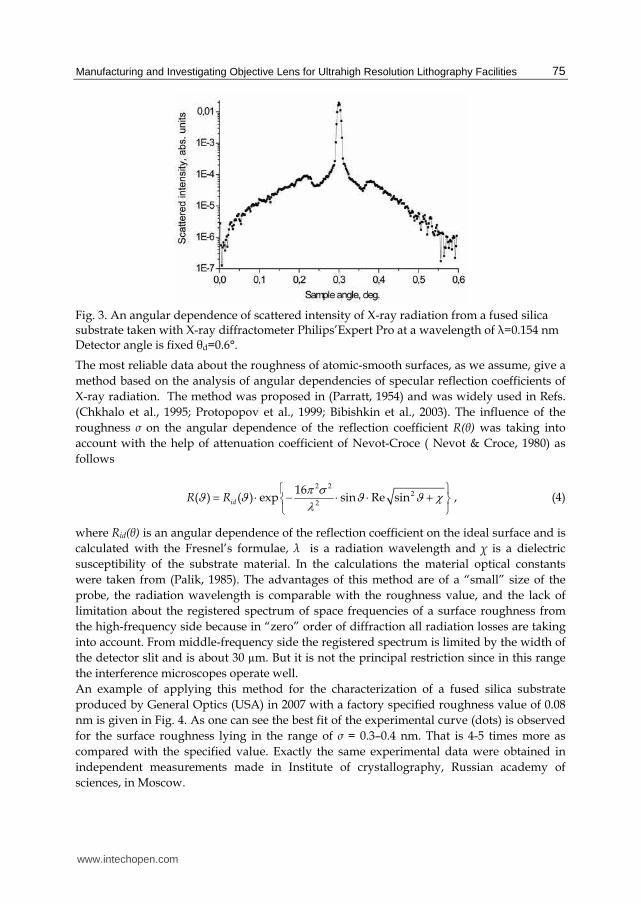
Manufacturing and Investigating Objective Lens for Ultrahigh Resolution Lithography Facilities
75
Fig 3 An angular dependence of scattered intensity of X-ray radiation from a fused silica substrate taken with X-ray diffractometer PhilipsrsquoExpert Pro at a wavelength of =0154 nm Detector angle is fixed θd=06deg
The most reliable data about the roughness of atomic-smooth surfaces as we assume give a method based on the analysis of angular dependencies of specular reflection coefficients of X-ray radiation The method was proposed in (Parratt 1954) and was widely used in Refs (Chkhalo et al 1995 Protopopov et al 1999 Bibishkin et al 2003) The influence of the roughness σ on the angular dependence of the reflection coefficient R(θ) was taking into account with the help of attenuation coefficient of Nevot-Croce ( Nevot amp Croce 1980) as follows
2 2
22
16( ) ( ) exp sin Re sinidR R
π σϑ ϑ ϑ ϑ χλ⎧ ⎫= sdot minus sdot sdot +⎨ ⎬⎩ ⎭ (4)
where Rid(θ) is an angular dependence of the reflection coefficient on the ideal surface and is calculated with the Fresnelrsquos formulae λ is a radiation wavelength and is a dielectric susceptibility of the substrate material In the calculations the material optical constants were taken from (Palik 1985) The advantages of this method are of a ldquosmallrdquo size of the probe the radiation wavelength is comparable with the roughness value and the lack of limitation about the registered spectrum of space frequencies of a surface roughness from the high-frequency side because in ldquozerordquo order of diffraction all radiation losses are taking into account From middle-frequency side the registered spectrum is limited by the width of the detector slit and is about 30 microm But it is not the principal restriction since in this range the interference microscopes operate well An example of applying this method for the characterization of a fused silica substrate produced by General Optics (USA) in 2007 with a factory specified roughness value of 008 nm is given in Fig 4 As one can see the best fit of the experimental curve (dots) is observed for the surface roughness lying in the range of σ = 03ndash04 nm That is 4-5 times more as compared with the specified value Exactly the same experimental data were obtained in independent measurements made in Institute of crystallography Russian academy of sciences in Moscow
wwwintechopencom
Lithography
76
Fig 4 Angular dependencies of reflection coefficients of radiation with λ=0154 nm from a fused silica substrate made by General Optics dots correspond to experiment solid lines are calculations corresponding to different roughness values
The investigation of this substrate by means of an atomic-force microscopy carried out in our institute has shown a strong dependence of measured roughness on the probe size When we use Si-cantilever the measured roughness was about 008 nm but with a wicker the value has increased up to 016 nm So this direct comparison of the application of X-ray reflection and atomic force microscopy for atomic-smooth surface roughness measurement indicates that the latter method gives an underestimated value of the roughness A serious disadvantage of the specular X-ray reflection method is that it allows studying only flat samples while components of imaging optics have concave and convex surface shapes Therefore in practice for evaluating the surface roughness of nonplanar samples it makes sense to use the atomic force microscopy method taking into account the calibration of X-ray reflection made with flat substrates In conclusion it should be noted that a large body of research done with the help of the x-ray specular reflection method to measure a surface roughness showed that a number of substrates fabricated in different countries had a minimal surface roughness 02-03 nm and included crystal silicon used in electronic industry The minimal surface roughness of fused quartz substrates were in the range of 03-04 nm except for the case (Chkhalo 1995) where the roughness of 025 nm is reported
4 Investigating the surface shape by means of optical interferometry
Optical interferometry is one of the most powerful and widely used method for measuring a surface shape of optical components and wave front aberrations of complex systems in the industry The main advantages of the inetrferometry are the simplicity and high accuracy of the measurements The investigation technique is based on the analysis of a light intensity distribution over interference patterns In this paragraph the basic principles of a surface shape and wave front distortions of optical component and system reconstruction with the use of data obtained by optical interferometers are described Both types of interferometers
wwwintechopencom
Manufacturing and Investigating Objective Lens for Ultrahigh Resolution Lithography Facilities
77
are considered conventional utilizing reference surfaces and diffraction using as a reference a spherical wave appeared due to the diffraction of light on a wave-sized pin-hole
41 Shape reconstruction and interferometry utilizing reference surfaces At present a gamma of interferometers is used in an optical industry including Fizeau and Twyman-Green interferometers which stand out because of their simplicity in operation high accuracy and universality is developed A detailed description of these instruments can be found in many books for instance (Malacara 1992 Okatov 2004) Independently on an optical scheme in this type of instruments the interference patterns are detected which appear as a result of the interaction of two waves reflected from studied ES (a surface with defects in Fig 5) and from reference ER (top surface in Fig 5) surfaces As a result the fringes
Fig 5 A fringe pattern formation by interfering of two waves reflected from a surface under study (bottom) and a reference (upper) one
of so called ldquoequal thicknessrdquo are observed A defect on the surface under study marked in Fig 5 by symbol z with a height of h gave rise the phase shift of the reflected light according to
2 2 hπ δ λΔ = sdot (5)
where λ is a wavelength The corresponding fringe banding z induced by the deviation of the studied surface from the reference can be found from the ratio
( 2) h z zδ λ δ= sdot (6)
These expressions in particular allow to see that the defect with the height of λ2 corresponds to one fringe in the interference pattern When the defects on the studied surface are absent the fringes make a system of equidistant straight lines In such a manner the interference pattern uniquely determines the local shape deviations of the surface under study from the reference So the task of the surface shape reconstruction needs looking for a mathematical model which will fit the experimental data the best
( ) ( )W x y h x y= Δ (7)
where ( )h x yΔ is the surface deformation in respect to the reference and being a function of coordinates on the surface x yisinΩ Ω is an operating range of the surface As a rule the
wwwintechopencom
Lithography
78
sought-for function (Braat 1987) is written in terms of some basis of functions and its description reduces to finding a set of the series coefficients ck
( ) ( )k kk
W c α=sumr r (8)
where r is a radius-vector of a point on the surface and ( )kα r is a set of basis functions Mostly common polynomials orthogonal on some area 0Ω are chosen as the basis For instance for the circular area these are Zernike polynomials which are widely used in optics (Rodionov 1974 Golberg 2001) The orthogonality of the polynomials results in the fact that each term of the series makes a contribution independent on the remaining terms into the mean-square of the wave front deformation Since the representation of the investigated function is global any local dilatation when approximating is smoothed thus distorting global view of the function Besides when reconstructing the surface shape it is important to evaluate not only the global surface shape but local errors too From this it follows that the mathematical model should be oriented on the description of the surface shape not only globally but locally too In the framework of this paper this dilemma was solved by introducing local deformations additionally to the global description (8) of the surface deformation function
0( ) ( ) ( )k k mj jk m j
W c cα β⎡ ⎤= + sdot minus⎢ ⎥⎢ ⎥⎣ ⎦sum sum sum mr r r r (9)
where cmj and j are coefficients and ldquospecialrdquo basis functions describe a m-th local deformation with the center in the point with the coordinate of r0m It is significant that the set of functions k(r) and j(r-r0m) are different in general case because the described function W(r) should not be interrupted in the range of definition It is the reason why the ldquospecialrdquo functions j(r-r0m) must be finite should not have discontinuity and their values at the definition range boundary must be equivalent to zero An algorithm of searching for the expansion coefficients of the surface model (9) was performed in two stages At the first stage the global surface shape error is approximated according to the (8) model At the second stage the residual local surface deformations are approximated by the right part of the expression (9) In our case the global description of the surface shape errors is performed with the help of Zernike polynomials WZ() and the residual local dilatations ndash by using the apparatus of local splines WS() which advantages when describing the optical surface deformations are analyzed in (Archer 1997 Sun et al 1998) in details
0 0 0 0
0 0
( ) ( ) ( ) ( )cos( ) ( )sin( )
( sin( )) ( cos( ))
Pz n Pz nm m
Z S nm n nm nn m n m
k k
i P j P ijS Si j
W W W c R m s R m
B B P
ρ ϕ ρ ϕ ρ ϕ ρ ϕ ρ ϕρ ϕ ρ ϕ
= = = =
= =
= + = + ++ sdot sdot sdot
sumsum sumsumsumsum (10)
where and are polar coordinates of the point on the surface cnm and snm are the expansion coefficients ( )m
nR ρ are radial Zernike polynomials BiPs is the basic function of the -spline of the order of pS on i-th interval of y coordinate and BjPs ndash is the basic function of the -spline of the order of pS on j-th interval of x coordinate and Pij corresponds to the
wwwintechopencom
Manufacturing and Investigating Objective Lens for Ultrahigh Resolution Lithography Facilities
79
points of control of the spline A number of works (Rodionov 1995 Swantner amp Weng 1994) are devoted to the methods for determining the coefficients of the mathematical model of the surface shape deformation function (10) by using interferometric data In present work algorithms and programs developed in (Gavrilin 2003) are used Currently available methods of digital registration and mathematical processing of interferograms allow reconstructing the surface shape (wave front aberrations) in respect to the reference surface Fig 5 with the accuracy up to 10000 where is an operating wavelength of the interferometer However the guaranteed surface shape accuracy of the reference in the root-mean-square (RMS) does not exceed 30 ndash 20 (Website Zygo 2009) that is two orders of magnitude worse than required for instance for projection nanolithography optics A substantially better situation is observed when studying surfaces at typical scales lower than 1 mm At these scales the accuracy of the reference surfaces is better than 1000 that allows measuring the surface shape deformations with the sub-nanometer accuracy On this basis a number of micro-interferometers with a digital fringe registration has been developed in the last few years (Blunt 2006 Chkhalo et al 2008 Website Veeco 2009 Website Zygo 2009) Below the spectrum of space wavelengths on the surface under study to be registered and where the surface shape measuring by interferometers with the sub-nanometer accuracy is limited by the lateral resolution of a microscope is given typically lies in the range of 03-1 microm
42 Interferometers with a diffraction reference wave The problem of conventional interferometers using the reference surfaces is solved by the application of interferometers with a diffraction wave as the reference proposed by VP Linnik in 1933 (Linnik 1933) The proposal is based on the theoretical fact that when a flat electromagnetic wave falls onto a pin-hole with a diameter comparable with a wavelength in an opaque screen consisting of a zero-thickness superconducting material diffracted behind the screen wave in a far wave zone is an ldquoidealrdquo sphere (Born amp Wolf 1973) This feature of the light diffraction was used as the basis for developing interferometers of this type The first interferometer attended to the investigation of optics with sub-nanometer accuracy for the EUV nanolithography has been made by GE Sommargren in 1996 As a source of the reference spherical wave he used a single-mode optical fiber with a core diameter (exit aperture) of about 4-5 microm The objective for a projection scheme of a EUV-nanolithographer was tested with the help of the interferometer (Sommargren 1996) The author evaluated the measurement precision in terms of the RMS at the level of 05 nm With a high-coherence laser the interferometer allowed testing a surface shape of individual optical elements The main disadvantage of the interferometer was a ldquobigrdquo source size A numerical aperture where the diffracted wave still remains ldquoan ideal sphererdquo is determined by expression NAref ltλd and in the case of λ=05 microm and d=5 microm corresponds to NAreflt01 Partly the low-aperture problem is solved at the expense of stitching measured data over different areas of the studied substrate or objective Along with the apparent loss of a measurement accuracy when using the stitching procedure there exists one even more serious disadvantage of using low-aperture interferometers associated with a strong irregularity of interferogram illumination Fig 6 demonstrates how the illumination irregularity results in error when determining the position of the fringe extremum In other words along with the apparent
wwwintechopencom
Lithography
80
loss of measurement accuracy connected with the stitching low-aperture interferometers have a significant systematical error induced by strong intensity anisotropy of the reference wave Therefore the recent trends are toward increasing the use of diffraction on man-made pin-holes in an opaque screen Modern microelectronic technologies provide manufacturing high-quality low-edge roughness pin-holes with diameters down to 40-50 nm
Fig 6 Shift of determined position of fringe maximum (systematic error) caused by the illumination irregularity
Such pin-holes are applied in diffraction interferometers operating at the working wavelength of a EUV nano-lithographer λ=135 nm which are installed on undulators of the last generation synchrotrons in USA and Japan (Naulleau et al 2000 Murakami et al 2003) An interferometer circuit installed on ALS (Berkeley USA) is given in Fig 7
Fig 7 Optical scheme of interferometer with diffraction reference wave installed on synchrotron ALS in Berkeley USA The picture is taken from (Medecki et al 1996)
The device operates in the following way The radiation falls onto a small pin-hole Gap installed on the lens object plane under study A diffracted ldquoidealrdquo spherical wave passing through the lens is distorted according to its aberrations and is collected in the image plane On the radiation way in-between the lens and the image plane a diffraction grating is installed which splits the wave-front into two ones corresponding to zero and to 1-st diffraction orders The zero-order radiation passes through the hole which diameter is big enough and exceeds a focusing spot thus preventing the distortion of the wave front The 1-st order beam is focused onto a small-size pin-hole Due to the diffraction behind the
wwwintechopencom
Manufacturing and Investigating Objective Lens for Ultrahigh Resolution Lithography Facilities
81
screen ldquoan idealrdquo spherical wave is generated The reference wave expands toward a CCD-camera where it interferes with a wave passed through the lens under test The measurement accuracy provided by the interferometer will be discussed later when comparing with our interferometer As we can see such interferometers are efficiently used for the final characterization of wave-front aberrations of objectives for EUV radiation At manufacturing stages of substrates and mirrors the producers of the optics usually use optical diffraction interferometers The experimental study of capabilities of point diffraction interferometers operating with a visible light has demonstrated a number of factors reducing the measurement accuracy Particularly systematic discrepancy of experimental data when studying the same optics with the help of visible and EUV light interferometers is observed (Goldberg et al 2002) All of this stimulated to study the way how finite conductance and thickness of the screen material have an effect on amplitude-phase characteristics of the diffracted wave behind the screen and correspondingly on the interferometer measurement accuracy In work (Chkhalo et al 2008) the calculations of the amplitude-phase characteristics of the diffracted field behind the screen in the far-field zone have been carried out They used the solution of a task about the field of a point source located above a half-space with arbitrary properties and covered with a film of any thickness and arbitrary optical constants given in (Dorofeyev et al 2003) Fig 8 illustrates the statement of the problem The diffraction of a flat wave on a circular hole with the radius of a in a film with thickness of hf and the inductivity of f in medias with parameters and 1 was considered The field was calculated behind the screen at Zgt0 on a spherical surface with a fixed radius R0=10 cm The radius R0 was chosen from practical reasons but its value does not produce any effect on the community of the result since the calculation was done for a case krgtgt1 where k=2λ is a wave vector of the diffracted wave in a point with the radius-vector r
Fig 8 Sketch of the geometry of the problem where hf is the thickness of the film heff is an effective film thickness (characterized by the skin-layer) d is the diameter of a hole 1 and f are the dielectric constants of the film and the medias θ1 and θ2 are the angles of diffraction Incident wave is schematically shown by the arrows
The results of the calculations as compared with the solution of classical task of diffraction on zero-thickness superconducting screen have shown that most real electrodynamical
wwwintechopencom
Lithography
82
characteristics of the screen material have an effect on phase characteristics of the diffracted field The calculation of the phase distortions was carried out for the films of aluminum molybdenum tungsten and a number of other materials The results of numerical calculations shown in Fig 9 represent a relative phase deviation on meridional angle of the diffracted scalar field in the case of aluminum different thickness films characterized by dielectric constant Alasymp-542-i218 at the wavelength 633 nm as compared with the case of a perfect screen |Al|rarrinfin The phase incursion ∆(θ) is expressed in nanometers The radius of the hole in the films was а=150 nm A case of free standing (=1=1) films was considered It is evident that the larger the meridional angle the larger is the phase deviation of the diffracted field in the case of a realistic screen We connect the result with an additional phase accumulation due to the field propagation through the real film at larger meridional angles (see Fig 8 for a qualitative clarification) We did not find a thickness dependence on the phase accumulation in the range of lthflt1000 nm where is a skin-layer because the phase can be effectively accumulated only inside the skin-layer The transitions hfrarr0 and |Al|rarrinfin |Al|rarrinfin or hfrarr0 led to the known textbook examples The corresponding diffraction fields for such idealized problems perfectly coincide with those of a spherical phase front
Fig 9 A relative phase deviation ∆(θ)=((0)-(θ))λ2 on meridional angle of the diffracted field in a case of Al different thickness film (Alasymp-542-i218) at the wavelength 633 nm on a spherical surface R0=10 cm the hole radius is а=150 せす
Other mechanisms of the phase distortion can be associated with the excitation of waveguide and surface modes in a plane layer and with a diffraction of such modes by a hole followed by their radiative decay Since the dielectric constant of all materials in soft X-ray and EUV ranges are close to unity Re()asymp1 corresponding phase distortions are minimal It is one of the reasons why the quality of the diffracted reference wave in EUV region has a better result in a higher measurement precision The carried out calculations have shown (see Fig 10) that the angular dependencies of the phase distortions on the meridional angle weakly change for different materials The only exception is osmium for which the phase deformation was extremely low Optical constants of materials used in these calculations were taken from (Palik 1985)
wwwintechopencom
Manufacturing and Investigating Objective Lens for Ultrahigh Resolution Lithography Facilities
83
Fig 10 Angular dependencies of the phase distortions on the meridional angle for different materials
By this means a fundamental limitation of the point diffraction interferometer measurement accuracy is caused by the aberrations of the reference spherical wave induced by the interaction and propagation of secondary waves through the screen material These aberrations are liable to reach a few nanometers depending on the angular aperture If we take into account the polarization characteristics of the light the aberration of the reference wave increases a few times depending on azimuth angle (Dorofeev 2009) The quality of a diffracted wave strongly depends on wave aberrations of preliminary optics focusing the laser beam and the accuracy of adjusting the laser beam axis in respect to the pin-hole center (Otaki et al 2002) All these limit the working aperture of the interferometer and result in the necessity of testing high-aperture optics zones The following stitching procedure of the zonal data raises additional errors All of these disadvantages hinder to widespread use of the point diffraction interferometers in an industry Taking into account all of these problems and limitations the problem of searching for alternative and more perfect methods for the spherical wave generation becomes very urgent
5 Spherical wave source on the basis of tipped fiber
The sources of the spherical wave based on tipped down to a sub-wave exit aperture of the single mode fibers are free from the many of mentioned above problems The application of such fibers as a reference spherical wave source for the point diffraction interferometers has been proposed in (Klimov et al 2008) In Ref (Chkhalo et al 2008) the aberrations of the wave generated by the sources at the wavelength of He-Ne laser =633 nm have been studied These investigations have demonstrated a number of advantages of spherical wave sources as compared with the conventional ones based on a pin-hole in an opaque screen One of the advantages is connected with the fact that in the optical fiber the eigenmodes are excited and correspondingly the quality of the diffracted wave does not depend on aberrations and the mechanical adjustment of the preliminary optics A high degree of homogeneity of the diffracted wave (dgt1) is combined with a high intensity because the light is input into the fiber using high-efficiency methods through a 5-
wwwintechopencom
Lithography
84
microm-diameter core The convex shape of the source Fig 11 decreases the ldquotiprdquo effect bound to the interaction of the off-axis rays with a metallized part of the fiber along the perimeter of the exit aperture The lack of a flat screen around the source significantly decreases diffracted wave distortions connected with the light polarization The well developed methods for handling optical fibers make it possible to easily control the polarization parameters of the diffracted radiation and implement various schemes for interference measurements For instance two or even more coherent sources can be organized with the given polarization of each other
Fig 11 Photographs of the fiber based source taken with scanning electron microscope (marked as a) and b)) and the source with on optical connector
The quality of the diffracted wave of the tipped fiber based source was studied with an interferometer (Kluenkov et al 2008) at two wavelengths =633 nm (He-Ne laser) and =530 nm (second harmonic of Nd-YAG laser) As opposed to the former experiments when in the measurement scheme an optical observation system collected the interfering fronts onto the CCD-camera in present work the data obtained by the direct detection of the fronts on the window-free CCD-camera are given As the experiments showed both the observation systems and even a thin glass window introduce a significant at the level of parts of nanometer error into the measurements
Fig 12 Experimental setup for studying the wave front deformations of the tipped fiber based sources of spherical wave 1 is a laser 2 is a system for input the light into the fiber 3 is a single mode fiber optics coupler 4 is a polarization controller 5 are sources under study 6 is a CCD-camera and 7 is a computer
wwwintechopencom
Manufacturing and Investigating Objective Lens for Ultrahigh Resolution Lithography Facilities
85
The new experimental setup is given in Fig 12 Polarization controllers (item 4 in Fig 12) allow to transform an elliptical polarization of the light at the output of the sources into a linear one as well as to superpose the polarization planes which provide the best contrast of the interference pattern The distance between the sources determining the fringe number (a wedge between two interfering wave fronts) was varied in the range of 1-10 m The measurements were carried out for different angles between the source axes The numerical aperture was varied by approaching (moving off) the CCD camera in respect to the sources A typical interferogram and a wave aberration map obtained in the experiments are shown in Fig 13 The operating wavelength was =530 nm
Fig 13 A typical interferogramm and a wave aberration map observed in the experiments obtained at a wavelength =530 nm
The measured dependencies of the wave deformation RMS on numerical aperture NA of this couple of sources are given in Fig 14 The pictures correspond to the measurements in small (left) and in large (right) numerical apertures Left graphs on both pictures correspond to the experimental data The data obtained with the interferometer installed on the synchrotron ALS in Berkeley USA are marked by stars The interferometer using a pin-hole in an opaque screen as a reference spherical wave source operates at the wavelength =135 nm and is considered as a reference for the measurement accuracy among the point diffraction interferometers (Naulleau et al 1999) It is clearly seen from the pictures that wave front aberrations of the source developed in this work are even less as compared with the ALS-sources despite a longer operating wavelength When analyzing the obtained experimental data there is a need to pay attention to two facts bull Relatively ldquohighrdquo of order λ1000 total aberration of the diffracted waves is observed
at large numerical apertures (NAasymp03) bull Regular structure (symmetry) of the wave front deformation map is clearly seen Such maps and statistical values of the deformations are practically found for all couples of so called ldquohigh qualityrdquo sources The wedge direction between interfering fronts (a line passing through the sources) represents itself as the axis of the symmetry Particularly the deformation map can be put ldquohorizontallyrdquo by turning the wedge through 90 degrees All of this points to the presence of an aberration caused by some kind of physical reason rather than by technological fluctuations This aberration rises with the increase of the observation angle just as it is shown in Figs 9 and 10 In case of understanding the physical nature of this aberration it can be taken into account when reconstructing the true wave deformation (surface shape) that results in increasing the working aperture of the interferometer by a few times
wwwintechopencom
Lithography
86
Fig 14 Averaged over 9 measurements total wave front deformations of couple of the fiber based spherical wave sources depending on numerical aperture (left graphs in both pictures) and ALS-data (Naulleau et al 1999) (stars) Working wavelength is =530 nm First picture corresponds to lower and right ndash to the higher numerical apertures The right graphs in the pictures are corrected according to the geometry of the experiment
This fact of the uniform angular dependence of the aberration let us interpret in a new manner the measurement data obtained in ALS and in our experiments In the Youngrsquos experiment carried out in ALS the least distorted parts of the diffracted waves round their own axes interfere Correspondingly RMS of the aberration is calculated over the range of the cone limited by the numerical aperture NA Opposite to that in our case side parts of the wave fronts interfere Fig 12 in the range from zero degree up to a double value of the angular aperture of the wave front In other words in the search for the wave front aberration RMS the averaging is performed over a double numerical aperture 2NA Therefore the measured dependences presented in Fig 14 (left graphs) can be corrected in the manner as it is shown by arrows (right graphs) As it is seen from the picture the source of the reference spherical wave based on a tipped single mode fiber has a substantially lower wave front aberration and a higher working aperture as compared with the conventional one based on pin-hole in an opaque screen
6 Diffraction interferometer based on a single mode fiber with the sub-wave exit aperture
On the basis of a tipped fiber source of the reference spherical wave the laboratory sample of an interferometer has been developed and manufactured which optical scheme and photo are presented in Figs 15 and 16 The interferometer is installed in a basement thermostated room on a bearer separated from the house footing For the additional protection against vibrations the instrument is installed on 12 bellows under 16 bar pressure Since the measurement accuracy is extremely high the turbulent air flowing inside the interferometer and effecting optical paths along the rays can introduce additional errors To solve these problems the interferometer is placed into a vacuum chamber which is pumped out down to a pressure of 1 Pa
wwwintechopencom
Manufacturing and Investigating Objective Lens for Ultrahigh Resolution Lithography Facilities
87
Fig 15 Optical scheme of the interferometer 1 ndash PC 2 ndash registering system 3 ndash observing system 4 ndash source of spherical wave 5 ndash flat sharp-edge mirror 6 ndash three-axes-controlled precision bench 7 ndash tested concave surface 8 ndash single mode optical fiber 9 ndash polarization controller 10 ndash laser
Fig 16 Photograph of the vertical vacuum interferometer
wwwintechopencom
Lithography
88
The optical scheme shown in Fig 15 corresponds to the interferometer for studying concave spherical or weakly aspherical surfaces The spherical wave source (item 4 Fig 15) is mounted on a high-precision three-axis-controlled bench (item 6 Fig 15) in the direct in a distance of several micrometers proximity from the flat mirror (item 5 Fig 15) The reference spherical wave which after reflecting from the studied surface (item 7 Fig 15) carries the information about its form is focused on a flat mirror and being reflected from it goes into the CCD registering system where it interferes with a part of the reference front directly propagating to the detector The main disadvantage of this scheme is connected with the fact that the investigated sample is irradiated by the most distorted side part of the wave front that practically halves the interferometer operating numerical aperture For solution of this problem in (Kluenkov et al 2008) the scheme of the interferometer with two low-coherent sources of the reference spherical waves has been proposed (Fig 17) In this scheme one source forms the spherical wave laquoSpherical wave 1raquo irradiating the investigated surface while the spherical wave of the second source laquoSpherical wave 2raquo is directed into the registering system The radiation reflected from the investigated surface contains the information on its shape and after reflecting from the flat mirror is directed to the registering system where interferes with the reference laquoSpherical wave 2raquo The main advantage of the scheme is that the axes of the wave fronts coincide with the axes of the investigated surface and the registering system which provides the minimal deformations of reference fronts
Fig 17 Scheme of the low-coherence diffraction interferometer with two sources of the reference spherical wave
As a source of the radiation a super-luminescent diode with a coherence length about 20 microns is applied It prevents parasitic interferences of wave fronts produced by different elements of the optical scheme For observing the correct interference the optical path of the light of source 2 is increased by a double distance from the investigated surface to the sources In this case the interference is observed only for the noted above wave fronts The radiation of the source 1 directly going into the registering system creates only a background signal on the detector
wwwintechopencom
Manufacturing and Investigating Objective Lens for Ultrahigh Resolution Lithography Facilities
89
As it was already marked in diffraction interferometers a divergent spherical wave is used as a reference wave It imposes a number of restrictions on the interferometer capabilities Strictly speaking with their help it is possible to investigate only concave spherical and slightly aspherical surfaces and objectives The measurement of the form of strongly aspherical concave or even spherical but convex surfaces demands using additional optical elements transforming the reference divergent spherical wave to a new one which front is close to the surface shape under study Of special interest are interferometric measurements of objective wave front deformations for example for final certification of the objective wave aberrations or for objective adjustment directly in an interferometer or in the case of the objective application for studying convex spherical surfaces In Fig 18 the scheme and photograph of measurements of six-lens objective in the interferometer are shown In this scheme two coherent sources are used The measured data of the wave deformation were PV = 423 nm and RMS = 82 nm
Fig 18 Scheme of the interferometer with two coherent sources of the reference spherical wave (left) and photograph in the interferometer (right) for testing sixs-lens objective 1 ndash PC 2 ndash registering system 3 ndash observing system 4 ndash source of spherical wave 5 ndash flat sharp-edge mirror 6 ndash three-axes-controlled precision bench 8 ndash single mode optical fiber 9 ndash polarization controller 10 ndash laser 11 ndash studied objective
The certified objective was used for the interferometric measurement (Fig 19) of a convex spherical surface of a special compensator which in turn later on was applied for studying the concave ashpherical surface for a double-mirror objective For reconstructing the true shape of the convex surface the expansion coefficients at basis polynomials corresponding to the objective aberrations were deducted from the measured ones Aspherical surfaces are used in the majority of high-resolution optical objectives in order to widen the field of view of the optical systems Direct testing of aspherical surfaces by using an interferometer with the spherical reference wave is often difficult or even impossible For example Fig 20 a) shows the interferogram for a concave aspherical substrate with about 7-microm deviation of the surface from the nearest sphere The measurements were carried out by using the basic scheme shown in Fig 15 It is evident that a large number of fringes makes
wwwintechopencom
Lithography
90
the position determination of the minima almost impossible Moreover the upper part of the interferogram is simply not there which is explained by a large about 100 microm diameter of the focusing spot for which the beam partially propagates above the edge of mirror (item 5 Fig 15) and misses the measurement system
Fig 19 Optical scheme (left) and photograph of units (right) in the interferometer for certification of convex surfaces Designations on the scheme are the same as in Fig 15
Fig 20 Interferograms from the aspherical concave mirror М2 obtained without wave-front corrector (a) and using corrector (b)
One of the most effective solution of this problem is the use of wave-front correctors ie special optical elements that transform a reference spherical wave front into an aspherical one which shape is identical to the shape of the studied surface In order to take into account the wave-front distortions due to errors of the corrector itself its surfaces should be only spherical In this case it is possible to test these surfaces with subnanometer accuracy by using a spherical reference wave interferometer by the techniques stated above The scheme for testing the concave aspherical surface by using a corrector is presented in Fig 21 The parameters of the corrector suitable for testing the concave aspherical surface
wwwintechopencom
Manufacturing and Investigating Objective Lens for Ultrahigh Resolution Lithography Facilities
91
ie radii of the surfaces thickness and the distance from the reference wave source to the top of the first surface were calculated by minimizing the difference of longitudinal aberrations of the tested aspherical surface and the corrector described in (Malacara 1992 Puryaev 1976) in detail The calculated root-mean-square deviation of the wave front after the corrector from the investigated aspherical shape was RMS=λ1810 This suffices for testing the mirror surface of a nanolithographer with a double-mirror objective It is clearly seen from Fig 20 b) that the interferogram from the aspherical surface obtained by using such a corrector can be reliably processed
Fig 21 Optical scheme (left) and photograph of units in interferometer (right) for certification of concave aspherical surfaces using corrector 1 - computer 2 - registering system 3 - observation system 4 - spherical wave source 5 - flat mirror 6 - 3D precision table 7 - investigated concave aspherical surface 8 - optical fiber 9 - polarization controller 10 - laser 11 - corrector
The analysis of the influence of misalignment in the measurement optical scheme and a thickness error of the compensator on ldquoasphericityrdquo of the wave-front passing through the corrector and accordingly on the measurement accuracy has shown that the requirements for these characteristics of the optical scheme are easily performed in practice In particular the error of a compensator thickness within the limits of plusmn01 mm leads to a wave front aberration at the level of λ1000 Studying of the convex aspherical surfaces is complicated by the fact that besides the corresponding transformation of a spherical front into an aspherical one the corrector must provide a converging front of the wave All of these essentially complicate both the calculation and the design of the corrector In particular in some cases it is necessary to use aspherical surfaces or more than one lens In the case of optics for Schwarzschild objectives this problem is solved easily enough As a corrector the mating concave aspherical mirror which surface has been preliminary tested by using the corrector system described above and corrected according to the procedure described in the next section can be used The measurement scheme is presented in Fig 22 This scheme can be applied for the final
wwwintechopencom
Lithography
92
adjustment and certifications of the objective It is noteworthy to mention that this method can be applied for a convex spherical surface characterization too besides using additional objectives as it is shown in Fig 19
Fig 22 Measurement scheme of aspherical convex mirror М1 using mirror M2 as a wave-front corrector 1 - computer 2 ndash CCD camera 4 - spherical wave source 9-polarization controller 10 ndash laser 11 ndash Schwarzschild objective М1 and М2 ndash convex and concave aspherical mirrors
The measurement accuracy provided by the interferometer depends on many factors including the quality of the reference-wave source the accuracy of determining the positions and a number of interference minima and the accuracy of mathematical retrieval of the surface (wave-front) shape using a limited number of experimental points and the number and degree of the polynomials In turn the accuracy of determining the minimum positions is strongly dependent on the width of the interference pattern the degree of pollution of the interference pattern by ldquoparasiticrdquo interference the method of its rejection the uniformity and intensity of the interfering fronts and a number of other unmanageable factors In this work the interferometer measurement precision was evaluated by studying the rotations of the measured surface maps corresponding to the physical turn of the tested detail The idea of this method is the following If the interferometer provides zero-error measurements then when the detail is rotated the measured surface map should turn correspondingly and the measured statistical parameters of the surface shape deformations should remain unchanged The measured surface deformation maps of a spherical substrate with a numerical aperture NA=014 corresponding to different rotations of the detail are
wwwintechopencom
Manufacturing and Investigating Objective Lens for Ultrahigh Resolution Lithography Facilities
93
presented in Fig 23 The figures demonstrate that the turn of the maps is well observed and the statistical parameters of the deformations change within the limits of RMS=307plusmn0055 nm This test confirms the high measurement accuracy provided by the interferometer which is sufficient for many lithographic applications
Fig 23 Maps and statistical parameters of the surface form deformation corresponding to rotations of the spherical mirror by 0 90 180 and 270 degrees
To summarize this section it is possible to ascertain that the developed interferometer with the diffraction reference wave provides a precision certification of the high-aperture optical surfaces and systems to the subnanometer accuracy
7 Shape correction of optical surfaces to subnanometer accuracy
The developed precise techniques for measuring the shape of optical surfaces made it possible to pass to the main stage the correction of the surface shape made with traditional accuracy λ2 - λ20 depending on the type of optics up to λ1000 - λ2000 In the context of the given work two methods of correction have been developed a vacuum deposition of thin film coatings and ion etching of previously deposited films through metal masks An extremely high accuracy of correcting the surface shape imposes specific requirements on the correction method 1 As a result of the correction process the microroughness of the corrected surface (as a
rule it is initially supersmooth) should remain at the initial level
wwwintechopencom
Lithography
94
2 In the case of a shape correction by means of a local thin film deposition the correcting layers should not distort the substrate surface shape due to intrinsic stress ie they should have a minimally possible stress
3 The correction method should provide the deposition or the removal of materials in a wide range of thickness (1-300 nm) with the accuracy not worse than several percents This problem is especially urgent in the last correction stages when the thickness of the layers to be deposited (removed) is about one nanometer
4 The film materials should allow their complete removal from the substrate (for example chemically) without changing the initial surface shape and microroughness It allows repeating the correction process in the case when the previous correction attempt failed
Researches on stress compensation in multilayer structures and on a substrate restoration have shown that a material meeting all these requirements is CrSc multilayer structure (Salashchenko 2001) The deposition of coatings was made by the magnetron sputtering method The scheme of the correction process and the photograph of the installation are shown in Fig 24 Vacuum in the chamber was (07-1)middot10-6 Tor pressure of working gas (argon) was (07-09)middot10-4 Tor The characteristic power on DC magnetrons was 300-400 W The film thickness control of the deposited layers is performed by variating the passage speed of the corrected surface above the magnetrons sources The stabilization of the discharge power and the argon pressure were provided at the level of 01 The predetermined distribution of the layer thickness over the substrate surface was reached due to the application of figured diaphragms mounted between the magnetron sources and the substrate In addition the substrate rotates around its axis Local values of the film thicknesses over the substrates were measured with an x-ray reflectometer at 447 nm wavelength The details of these measurements will be shown below
Fig 24 Photograph of a technological facility and scheme of surface shape correction by means of multilayer film deposition through masks
The operational experience with this technology has shown a number of important advantages Firstly the roughness of the film surface practically does not depend on the angle of incidence of the atoms in respect to the substrate that allows to carry out the
wwwintechopencom
Manufacturing and Investigating Objective Lens for Ultrahigh Resolution Lithography Facilities
95
correction procedure at normal angles It reduces shadows on the surface increasing the localness of the correction correspondingly Secondly the high accuracy of the layer thickness control up to 1 provides a high reproducibility of the process The film-correction method proved to be efficient for initial stages in which the layers with of tens-hundreds nanometers are deposited in a single correction The process becomes unstable as the thickness of deposited layers decreases down to the units of nanometers Correcting films have changed the proper color that is connected with films oxidation at initial stages of deposition The distribution of oxygen in depth of scandium film obtained with the help of a secondary ion mass-spectroscopy (Drozdov et al 2009) is given in Fig 25 The figure shows an increased content of oxygen on the film surface and at the film-substrate interface Other serious disadvantages of the thin-film-correction method has a discrete and iterative character of the process After each iteration it is necessary to vent the vacuum chamber to make a new diaphragm to pump the chamber again All this strongly decreases the throughput of the process
Fig 25 The distribution of oxygen in depth of scandium film deposited onto Si-substrate
Therefore the application of ion-beam etching at the final correction stage looks very attractive This method allows in particular when focused ion-beams are used to realize the ldquomasklessrdquo correction without frequent opening of the installation to atmosphere Now this method is widely used for substrate form correcting and even for final ion-beam polishing in optical industry (Allen et al 1991 Chason amp Mayer 1993 Ghigo et al 2007) Recently an intensive literature has evolved which is devoted to the application of this method for the precision correction of substrates for projection EUV lithography (Dinger et al 2000 Murakami 2007) For the ion beams applied for the surface shape correction of substrates for EUV and soft X-ray optical elements a number of requirements are imposed the basic of which is the preservation of the surface roughness at an initial (supersmooth) level even when the removed layer depth reaches a few hundreds of nanometers Therefore an optimization of ion energy and incidence angles of the ions on the corrected surface at different depths of material removal is an actual problem Other problems inviting a further investigation are connected with some features of the ion-beam etching at an extremely small depth (asymp 1 nm) removal of materials The experiments have been performed on the installation (Fig 26) with the Cauphmanraquo type ion-beam source KLAN-103M (Website Platar Company 2009) The basic advantage of
wwwintechopencom
Lithography
96
this source is the possibility of working with small ion energies Еi = 50- 300 eV at a significant current density
Fig 26 Photographs of installation for substrates surface shape correction by ion-beam etching
The main characteristics of the ion source are the operating gas is argon or other inert gases the maximal diameter of the ion beam is 100 mm the maximal ion current is 100 mA the maximal ion current density is up to 23 mAcm2 the range of ion energy regulation is 50-1500 eV at the energy spread of plusmn3 eV the discharge working voltage is 35-50 V the thermo-cathode is made of thoriated tungsten (03 mm in diameter) filament Presence of charge-neutralizer (additional thermo-cathode) allows compensating the ion beam charge that provides using the ion source for correction substrates of dielectric materials too The measured dependence of the etching rate of CrSc coating on the removal depth taken at ion energy Еi=200 eV and grazing incidence angle of θ = 42ordm is shown in Fig 27 by dots It is evident that at the initial stage of the etching the removal is less than 120 nm practically a linear increase of the etching rate from the removal depth is observed At a very small etching depth h lt10 nm a wide scatter of the etching rate values is observed Considering the data of the secondary ion mass-spectrometry Fig 28 such a behavior of the etching rate can be explained by oxidation of the sample surface The etching rate of the oxide layer is significantly lower as compared with pure CrSc material If take this into account the calculated etching rate a solid line in Fig 27 matches well the experimental data The observed instability of the etching rate at h lt10 nm might be explained by the variation of the oxidized layer depth in various samples When samples were etched by a neutralized beam (stars in Fig 27) no changes of the rate were observed With the increased ion energy up to 300 eV Fig 29 such instability of the etching rate is not observed either According to atomic-force microscopy measurements the surface roughness remained constant at the level of 02 nm down to 400 nm removal depths For the ion energy of Еi=300 eV when the etching depth exceeds 80 nm an increase of surface roughness is observed (Fig 30)
wwwintechopencom
Manufacturing and Investigating Objective Lens for Ultrahigh Resolution Lithography Facilities
97
Fig 27 Dependence of etching rate on removal depth of CrSc multilayer structures dots are experiment with ions stars are experiment with neutrals and line is calculation accounting etching of the oxidized layer Ion energy Еi = 200 eV and current Ii=60 mA
0 5 10 15 20 25 30 35 40 4500
40x104
80x104
12x105
16x105
Oxigen
SIM
S in
ten
sit
y a
u
Depth nm
Fig 28 Typical distribution of oxygen atoms on depth of CrSc multilayer structure taken by secondary ion mass-spectrometry
The dependences of etching depth on an ion dose (the dose is the product of ion current and etching time) both from the ion current at fixed time and from the time at fixed current show a good linearity that is useful from the practical point of view because it allows to easily define the necessary etching time at a given ion current The example of the dependences of the etching depth on the dose is given in Fig 31 The dashed line corresponds to the linear approximation of the dependence and line with squares represents the experimental data It should be noted that the experiments carried out with greater ion energies up to Ei=15 keV have shown a fast growth of the surface roughness even at small nearby 20ordm grazing angles of incidence of the ions on the surfaces (Chkhalo et al 2008)
wwwintechopencom
Lithography
98
Fig 29 Dependence of ion etching rate on etching depth of CrSc multilayer structures at ion energy Еi = 300 eV (area of small removal depths)
Fig 30 Dependence of surface roughness of CrSc multilayer structures on etching depth at sputtering by argon ions with energy Еi = 300 eV
Fig 31 Dependence of etching depth of the CrSc multilayer structures on ions doze at ion energy Еi = 300 eV - - - linear approximation of the dependence
0 20 40 60 80 1000
10
20
30
40
Etc
hin
g d
ep
th n
m
Dosage mAmin
wwwintechopencom
Manufacturing and Investigating Objective Lens for Ultrahigh Resolution Lithography Facilities
99
For correcting the surface shape of substrates for imaging X-ray optics when the subnanometer form accuracy is required the following strategy providing minimal time expenses has been chosen At the initial stage when peak-to-valley values (P-V) of the surface shape are 50-200 nm the local deposition of the thin films is applied Then at the reduction of the P-V values down to 10-20 nm the ion beams with the energy of 200 eV are used At the final correction stage the 300 eV-ions are applied Figure 32 illustrates the result of using this correction procedure for a spherical substrate with a numerical aperture of NA=025 (the diameter is 130 mm and the curvature radius is 260 mm) which was initially the standard etalon for a conventional interferometer The initial surface map is shown in Fig 32 a) The parameters of the surface were P-V=426 nm and RMS=73 nm The surface shape improved to P-V=73 nm and RMS=06 nm (Fig 32 b)) Thus a root-mean-square deviation of the initial surface shape from an ideal sphere has decreased in 12 times ie in units of the interferometer working wavelength (=0633 microm) it has became better than λ1000 The photograph of this mirror mounted on a metal frame is given in Fig 33
Fig 32 Maps of deviations of the spherical surface shape from the nearest ideal sphere a) initial shape (P-V=426 nm RMS=73 nm) b) after 12-th correction (P-V=73 nm RMS=06 nm)
Fig 33 Photograph of the multilayer spherical mirror for 135 nm wavelength in the frame Diameter of the working aperture is 130 mm
wwwintechopencom
Lithography
100
In spite of a greater wavelength of the traditional deep ultraviolet lithography (193 nm) because of a great number of lens and high requirements for the quality of the projective objectives the methods of correction and certification with a subnanometer accuracy described in this article are urgent for the refracting optics too In connection with this the researches on etching of fused quartz surfaces by ion beams with a compensated charge have been carried out As well as in the case of metal surfaces the main attention was given to the etching rate to the reproducibility of the etching process and to the surface microroughness depending on the beam characteristics incidence angles and material removal depths In Fig 34 the dependences of quartz etching depth on the etching dose are presented The dashed lines in the figure correspond to linear approximations of the dependencies The ion energy was 200 and 300 eV the grazing incidence angle was 42ordm The comparison with similar dependences for CrSc Fig 31 shows that the etching rate of fused quartz is almost twice as much No nonlinearity at the initial stage of the etching is observed that on the one hand proves the hypothesis about the effect of the oxide layer in the case of CrSc material and on the other hand essentially facilitates the correction process
0 100 200 300 4000
50
100
150
200
250
300
350
Etc
hin
g d
ep
th n
m
Dosage mAmin
Fig 34 Dependences of the etching depth on the doze for fused quartz Etching is performed by argon ions with compensated charge and with energy Еi = 200 and 300 eV - - - - linear approximation of dependences
The data on the surface roughness of a fused quartz substrate etched by ions (neutrals) with energies of 200 and 300 eV for various removal depths measured by means of the atomic-force microscope and by x-ray diffractometry are presented in table 1 The substrates manufactured by General optics (USA) were used in the experiment The minimal roughness of initial surfaces measured with an atomic-force microscope was 013 nm and with the x-ray reflection it was about 04 nm From the table it is evident that atomic-force microscope measurements have shown a weaker influence of the etching process on the surface roughness in comparison with the roughness measurements made by the x-ray diffractometry method A more detailed discussion of this difference is beyond the given article Thus the presented experimental data show that these technologies of vacuum deposition and ion-beam etching in the aggregate allow to correct with a subnanometer accuracy the surface shape of optical elements practically of any materials (metals dielectrics semiconductors) with keeping the surface on a supersmooth level This technology is
wwwintechopencom
Manufacturing and Investigating Objective Lens for Ultrahigh Resolution Lithography Facilities
101
suitable for manufacturing elements for imaging x-ray optics and for high resolution systems in visible and deep ultra-violet ranges
Table 1 Roughness of fused quartz substrates depending on neutral (ion) energy and etching depths measured by atomic-force microscopy (AFM) and x-ray diffractometry (X-ray) methods
8 Reflecting multilayer interference mirrors
The final stage of manufacturing a precise mirror for ultrahigh resolution imaging x-ray optical systems is the procedure of the deposition of multilayer reflecting coating on a substrate A low polarizability of materials (le1) and correspondingly a small jump of the refraction factor Δn=00001-01 on the vacuum-material interface and a strong absorption of the radiation by all materials completely exclude the application of refractive optics in the extreme ultra-violet and soft x-ray ranges Because of a low reflection from one interface the reflection optics of normal incidence can be only interferential and the number of layers demanded for the achievement of a high reflectivity depending on a wavelength can reach a value of 102-103 The absorption of the radiation in multilayer structures leads to the fact that the reflectivity is always less than unity While choosing an optimal pair of materials providing a maximal reflectivity on a given wavelength the circumstance is often used that in the range of wavelengths directly adjoining the absorption edge of the material gt AE (AE is the wavelength of the material absorption edge) and coinciding with an anomalous dispersion of the optical constants the lowest absorption and the maximal polarizability of materials are observed For some materials in the field of K-and L- absorption edges the refraction factor can even exceed unity In Fig 35 the calculated spectral dependences of the maximal reflection coefficients for the most attractive pairs of materials in a spectral range of 3 - 16 nm representing the biggest interest for projection nanolithography and high resolution x-ray microscopy are shown The greatest experimental reflectivity about 70 was obtained at a wavelength of 135 nm The spectral range around λasymp67 nm (area of boron anomalous dispersion) is of interest for projection x-ray lithography However the reflectivity obtained here with LaB4C multilayer mirrors at a normal angle of incidence does not exceed 45-47 (Andreev et al 2009) that is not enough for lithographic applications
wwwintechopencom
Lithography
102
2 3 4 5 6 7 8 9 10 11 12 13 14 15 1600
01
02
03
04
05
06
07
08
CrSc
CrC
LaB
MoBe
MoSi
experiment
Refle
ctivity
Wavelength nm
Fig 35 Calculated (lines with symbols) and experimental (stars (Website ESRF 2006 Andreev et al 2003)) reflection coefficients of mostly attractive pairs of materials in X-ray and EUV ranges
On the short-wave length side the working wavelength of the normal incidence multilayer optics is limited by technology capabilities for depositing high-quality short period multilayer structures At present the shortest periods have multilayer structures based on WB4C (the period dasymp1 nm) (Vainer et al 2006 Platonov 2002) and CrSc (dasymp15 nm) (Salashchenko amp Shamov 1997 Website ESRF 2006) A number of special requirements are imposed on the multilayers which should be deposited onto substrates for imaging optics In particular to provide a constructive interference of the waves reflected from different interfaces the radiation wavelength λ the local angle of incidence ( )rθ f
and the period of the multilayer structure ( )d rf should satisfy
the Bragg condition
( )2sin ( )
d rr
λθ=f
f (11)
where rf is a radius-vector of a point of incidence of the radiation on the structure As the
incidence angles are a function of the coordinates it results in the necessity to deposit multilayer structures with a variable over the surface period so-called ldquogradedrdquo structures In some cases for example when the angular divergence of the X-ray beam falling on one point of the mirror surface exceeds the Braggrsquos peak width the multilayer structure should have a variable period on depth (Kozhevnikov et al 2001) One more important feature of multilayer structures for precise optics can be explained as follows For multilayer dispersive elements the maximum deviation of the local value of the period d from the nominal one is determined by the condition of synchronism of the waves reflected from various interfaces which can be expressed through the spectral selectivity of a mirror 1 S d d Nδλ λ δ= = cong (N is a number of periods) In the case of precision multilayer imaging optics when the required surface shape accuracy is at a subnanometer
wwwintechopencom
Manufacturing and Investigating Objective Lens for Ultrahigh Resolution Lithography Facilities
103
level to the synchronism condition an extra requirement for the preservation of the mirror surface shape is added For example for the well-known MoSi multilayer structure optimized on the wavelength of λ=135 nm the period is dasymp7 nm at a number of periods N asymp 40 Correspondingly the general thickness of the structure is L=Nd=280 nm The local error of the period of 1 will affect weakly on reflectivity however the surface shape of the mirror will produce a change of 28 nm which already can essentially produce an influence on imaging properties of the mirror From these simple estimations two important conclusions follow Firstly when designing and manufacturing the surface shape of a substrate it is necessary to take into account the real thickness of a multilayer coating which would be deposited onto the substrate Secondly it is necessary to provide a high at a level of 02-03 accuracy of local values of the period over the mirror surface Besides an intrinsic stress in the multilayer structures which can also deform the surface shape must be taken into account The estimation of the deformation x of a substrate with a diameter D a thickness hsub with the Yung modulus E and the Poisson factor ν on which a hf thick film with the intrinsic stress σ is deposited can be performed by means of equations
2
2
3
4
1
f
sub
h Dx
Y h
EY
σδ
ν
sdot sdot= sdotsdot= minus
(12)
For instance for optimized on maximum of the reflection coefficient MoSi multilayer structure (portion of Mo layer in the period =dMo(dMo+dSi) = 04) the stress in our case is about σ =-350 М『а (Fig 36) At deposition of such a multilayer structure (general thickness is L=Nd=280 nm) on a substrate of fused quartz with the diameter D=220 mm and thickness h=50 mm (Y=844 》а) the maximal deformation of the substrate surface would be about 17 nm that essentially exceeds an admissible level of the surface shape deformation of a mirror for EUV lithography Different groups solve this problem in different ways One the solution is the use of mirrors with a specified thickness ratio of molybdenum layer in the periods Mo asymp 05 - 07 when the stress is close to zero (Windt et al 1994 Zoethout et al 2003) The other solution consists in adding a third material into the periods for example Ru (Oshino et al 2003) However all these methods either because of a stronger absorption of EUV radiation or because of an interface roughness growth have smaller of 10-20 absolute values of the reflectivity In IPM RAS a technique of the stress compensation based on the use of special sublayers lying under the basic MoSi multilayer structure is under development For CrSc multilayer structures the stress is close to zero at γCr=dCr(dCr+dSc)asymp05 (Fig 37 (Andreev et al 2005)) At γCrgt05 a sign of the stress is positive on the contrary to the MoSi structures at γMo= 04 when it is negative The total stress σeff in the structure consisting of CrSc and MoSi multilayer films can be determined from a ratio
( ) ( )
( ) ( )Mo Si Mo Si Mo Si Cr Sc Cr Sc Cr Sc
eff
Mo Si Mo Si Cr Sc Cr Sc
d N d N
d N d N
σ σσ ⎡ ⎤sdot sdot + sdot sdot⎣ ⎦= sdot + sdot (13)
from which it follows that optimizing the composition and the thickness of CrSc layers it is possible to compensate the stress in the basic MoSi reflecting multilayer structure
wwwintechopencom
Lithography
104
Fig 36 Stress in MoSi multilayer structures depending on ratio of Mo layer in period γMo=dMo(dMo+dSi) at fixed period d=697 nm
Fig 37 Stress in CrSc multilayer structure depending on ratio of Cr layer in period γCr=dCr(dCr+dSc) at fixed period d=54 nm
In practice it is necessary to consider a process of the stress relaxation which depending on the structure and materials is variable over several days Totally the stress can change by tens percent An example of such a process is illustrated in Fig 38 in which the time dependencies of the stress in multilayer structures consisting of anti-stress CrSc sublayers and MoSi reflecting layers are presented The structures differ by thicknesses of the sublayers It is necessary to note that the stress value is affected not only by ratio of the layer thickness in the period but also by the period size and conditions in which the films were deposited For depositing multilayer structures a method of magnetron spattering is used in IPM RAS The method allows depositing films onto curved as well as flat substrates The conditions under which multilayer structures are deposited are briefly described in section 6 devoted to the correction of the substrate surface shape by the method of local thin-film deposition The facilities have from two to six magnetron sources that allows depositing at one technological cycle reflecting anti-stress and anti-diffusion barrier layers Now the
σ MP
a
-1000
-800
-600
-400
-200
0
200
400
600
02 04 06 08 10
γMo=dMo (dMo+dSi)
0
100
200
300
400
500
600
700
06 065 07 075
σ MP
a
γCr = dCr (dCr+dSc)
wwwintechopencom
Manufacturing and Investigating Objective Lens for Ultrahigh Resolution Lithography Facilities
105
technologies of depositing more than twenty various pairs of materials are developed It allows manufacturing optics for a whole x-ray and extreme ultra-violet spectral range More details about the properties of the multilayer structures can be found in (Andreev et al 2003)
Fig 38 Stress in MoSi multilayer structures with anti-stress CrSc sublayers versus of time a) - [(CrSc)times42 d=538 nm =067 (MoSi))times45 d=698 nm =04] and b) - [(CrSc)times40 d=538 nm =067 (MoSi)times45 d=698 nm =04]
A great volume of works high requirements for the coating quality and for accuracy of the period distribution over a substrate surface dictate the need for an operative information about characteristics of the deposited coatings with the purpose of correcting the technological process It is most convenient to perform such work with the presence of laboratory reflectometers allowing the investigation of multilayer structures on working wavelengths and located in the immediate vicinity of technologists Therefore laboratory reflectometers are constantly being developed and improved recently In Refs (Loyen et al 2003 Miyake et al 2003 Gulikson et al 1992) the specialized reflectometers for investigating multilayer optics in the range around 135 nm are described As a source of the soft x-ray and EUV radiation the laser plasma is used which arises due to the irradiation of solid-state targets by laser light with a power density about 109 Wcm2 For monochromatization the radiation spherical diffraction gratings operating at grazing angles are used The characteristic fluxes of the photons in the working range of wavelengths of 10-16 nm on the investigated samples with the probe beam size asymp 2 mm are 107 - 108 photons (01 nmtimess) The results of reflectivity measurements of MoSi multilayer mirrors in the area of 135 nm obtained with the help of these reflectometers as compared with the data obtained with a PTB-reflectometer (synchrotron BESSY-2 Berlin Germany which is considered as the reference one) have shown the coincidence of the measured reflection coefficients at a level of 3 and the resonant wavelength asymp 001 nm The basic disadvantages of these reflectometers in our opinion are a narrow range of working wavelengths and a low spectral resolution caused by the applied monochromator scheme The monochromator consists of two stationary slits and spherical (or toroidal) diffraction grating Scanning across the spectrum is carried out due to the diffraction gratings rotation around its axis According to this arrangement the position of the slits and the diffraction grating coincides with the Rowland circle (Rowland 1893) only for one
-30
-20
-10
0
10
20
30
50 100 15 200 250
Time hours
σ eff
MP
a
a)
t days
σ MPa
- 40
- 30
- 20
- 10
0
1 2 3 4 5 6 7 8 9
x
x
xx
x x
b)
wwwintechopencom
Lithography
106
wavelength that essentially limits the range where the spectral resolution of the monochromator is kept at the acceptable level of Δλapp asymp 001-002 nm The other factor limiting working spectral range of the reflectometer is the type of the used radiation source (laser plasma) which large size does not allow scanning by the entrance slit of the grating spectrometer Our group develops multilayer optics for a wide spectral range λ=06-50 nm and the monochromator spectral resolution up to 0003-0005 nm is frequently required Therefore in IPM RAS laboratory reflectometers on the basis of high resolution grating monochromators have been developed These monochromators have a movable entrance slit and diffraction grating (Chkhalo et al 1998 Zuev amp Mitrofanov 2002 Bibishkin et al 2004 Bibishkin et al 2005) In the reflectometrs the monochromators of type RSM-500 (Lukirsky et al 1967) and McPherson-247 (Website Mcpherson Company 2009) are used The photograph and optical scheme of the last generation reflectometer are given in Fig 39 Owing to such a spectrometer the kinematic scheme slits and diffraction grating are always located in the Rowland focusing circle so that the high spectral resolution of the device in the whole range of wavelengths is provided Two diffraction gratings with various radiuses of curvature cover this spectral range
Fig 39 Optical scheme and photograph of the reflectometer XRT - x-ray tube S1 S2 - entrance and exit slits AS VS - horizontal and vertical anti-scattering slits DG - diffraction grating TM - toroidal mirror M ndash probe beam intensity monitor MIS - investigated sample D ndash detector G5 ndash five-axes goniometer
In the reflectometer the radiation from the anode of the x-ray tube (XRT) through the entrance slit of the monochromator (S1) falls on the diffraction grating (DG) The diffracted monochromatic radiation according to the diffraction grating equation cosϕ - cosψ =mλD (m - the order of diffraction λ ndash a wavelength and D - the grating period ϕ and ψ angles of diffraction and incidence correspondingly) is focused onto the spectrometer exit slit S2 Scanning across the spectrum is carried out by linear moving of the diffraction grating and the exit slit with a simultaneous turn of the diffraction grating so that the condition Xl=Rgsdot sinψ where Rg - radius and Xl - distance between the diffraction grating center and the exit slit is satisfied An anti-scattering diaphragm (AS) reduces the intensity of scattered radiation at the output of the monochromator and limits the irradiated area of the diffraction grazing The monochromatic radiation by means of a toroidal mirror (TM) is focused on the investigated sample The other important function of the toroidal mirror is connected with a filtration of higher diffraction orders which is especially urgent when
wwwintechopencom
Manufacturing and Investigating Objective Lens for Ultrahigh Resolution Lithography Facilities
107
working with bremsstrahlung of the tungsten anode Radiuses of the toroidal mirror are chosen in such a way that in a horizontal plane the exit slit and in a vertical plane the source are imaged on the sample under study The studied sample is installed on a five-axis goniometer which photograph and scheme of movements are shown in Fig 40 The linear translation along X and Z axes the rotation around them (ω and ) and the inclination θ allow to insert any point of the sample under study with a diameter up to 300 mm into the x-ray beam The detector executes 2 rotation The additional inclination of the detector 2θ allows to increase the numerical aperture of the sample which can be tested up to NA=05
Fig 40 Photograph of the goniometer and scheme of movements provided by the goniometer
The concept of a spectrometer-monochromator with a movable slit and diffraction grating became possible only due to the application of the dismountable x-ray tube of an original design as the radiation source The advantages of classical sealed x-ray tubes are their small dimensions and weight simplicity in operation sufficient for reflectometric applications intensity of the x-ray radiation and long life-time However the application of these sources for precision reflectometry in soft x-ray and extreme ultra-violet ranges has shown that because of the fast contamination of the anode by products of thermocathode material erosion and hydrocarbons decomposition under a powerful electron-beam emission characteristics and life-time of the tubes collapsed when comparing with expected values For solving this problem in our work the tube was equipped with an ion-beam source for cleaning anodes from contaminations (Bibishkin et al 2003) It allows to work without opening the spectrometer and the tube to the atmosphere within several months thus approaching its operation mode to the traditional sealed X-ray tubes for hard X-rays The work is done on K L and M characteristic lines of target (anode) materials and on continuous bremsstrahlung spectrum of tungsten On one holder about 8 targets of various materials are installed It is necessary to note that frequently it is possible to use a few spectral lines from one target
wwwintechopencom
Lithography
108
As an illustration in Fig 41 the measured spectral dependence of reflectivity of MoSi multilayer spherical mirror shown in Fig 40 is presented The measurement has been performed with the reflectometer at an incidence angle of the radiation to the sample of 5ordm (from the local normal)
Fig 41 Spectral dependence of the reflection coefficient of MoSi multilayer mirror deposited onto spherical substrate Angle of incidence was 5ordm from the local normal
One more important advantage of the x-ray tube as a source of X-ray radiation is that in the field of wavelengths lt3 nm because of aberrations of spherical grating the spectral width of the probe beam is ΔGge 001 nm while the spectral resolution of short period multilayers reaches values Δ MIS lt001 nm Since the natural width of characteristic lines of some materials in this range is essentially less than this value this circumstance provides precision measurements of reflective characteristics of multilayer mirrors even when monochromator does not provide the demanded resolution Thus the developed in IPM RAS methods of multilayer coating deposition stress compensation in the film structures laboratory metrology of the mirrors at working wavelengths restoration of the substrates without any damage of the substrate surface shape and roughness allow us to make and certify high reflecting multilayer mirrors with a sub-nanometer level surface shape accuracy attended for super-high resolution imaging X-ray optics
9 Conclusion
In the given article the basic researches and the full cycle of developed in IPM RAS technologies and metrology techniques from the substrate surface shape correction to the deposition of multilayer coatings on them which are required for manufacturing high reflecting mirrors for diffraction quality imaging in the extreme ultra-violet and in the soft X-ray ranges are described As a whole it is evident that the problem of manufacturing such optics for high resolution EUV lithography and X-ray microscopy is already solved as a first approximation The further activity should be directed toward the increase of both in manufacturing accuracy of optical surfaces up to a level of RMS=01 nm and in the numerical aperture of objectives up to NA=04-06
0
10
20
30
40
50
60
70
126 130 134 138 142
Wavelength nm
Refl
ect
ivit
y
wwwintechopencom
Manufacturing and Investigating Objective Lens for Ultrahigh Resolution Lithography Facilities
109
In this connection upgrading the interferometric methods for surface shape measurements of optical elements and wave-front deformations of objectives first of all and regarding the increase of their working numerical aperture is a subject of current interest The diffraction interferometers utilizing the tipped fiber as a source of the reference spherical wave look rather attractive Owing to the simplicity of the design high intensity of the diffracted wave weak sensitivity to the adjustment in an optical circuit and a number of other advantages the interferometers which are simple in operation can be developed for the optical industry In the framework of the given article the problem arising when aspherical surfaces are under investigation of development and optimization of correctors transforming the reference spherical fronts into the aspherical ones which shapes are identical to the shapes of the studied surfaces was not practically discussed Meanwhile traditional lens null-correctors have limited capabilities rather complicated in manufacturing and expensive and demand complicated calibrating procedures for taking into account the wave-front distortions due to errors of the corrector itself In this connection diffraction correctors represent a significant interest (Akatov et al 2004) A gross potential for the surface shape correction of dielectric materials by means of ion-beams has RF-etching in chemically active environments The first experiments on etching of quartz substrates by means of the RF-etching have shown that the surface micro-roughness did not change down to the removal depths of a few micrometers (Akhsakhalyan et al 2008) The most serious problem on the way of manufacturing the effective optics for the soft X-ray radiation λlt10 nm is that reflection coefficients of the multiplayer mirrors are not sufficiently high Nevertheless the results that have been recently obtained in the field of the X-ray optics teams may be considered as a break-through because they lay the foundation of developing such important physico-technological directions as projection EUV nanolithography X-ray microscopy and extraterrestrial astronomy of the ultrahigh resolution
10 References
Akhsakhalyan AD Vainer YuA Volgunov DG Drozdov MN Kluenkov EB Kuznetcov MI Salashchenko NN Kharitonov AI amp Chkhalo NI (2008) Application of reactive ion-beam etching for surface shape correction of X-ray mirrors Proceedings of Workshop ldquoX-ray optics ndash 2008rdquo pp 26-28 Chernogolovka Moscow region 6-9 October 2008 p 26-28 IPTM Chernogolovka (in Russian)
Allen LN Keim RE amp Lewis TS (1991) Surface error correction of a Keck 10 m telescope primary mirror segment by ion figuring Proceedings SPIE Vol 1531 1991 pp 195ndash204
Andreev SS Bulgakova SA Gaponov SV Gusev SA Zuev SYu Kluenkov EB Luchin VI Lopatin AYa Mazanova LM Prokhorov KA Sadova EN Salashchenko NN amp Shamov EA (2000) Investigations in field of projection lithography of extreme ultraviolet region in Institute for physics of microstructures RAS Surface X-ray synchrotron and neutron investigations Vol 1 2000 pp 32-41 (in Russian)
Andreev SS Akhsakhalyan AD Bibishkin MS Chkhalo NI Gaponov SV Gusev SA Kluenkov EB Prokhorov KA Salashchenko NN Schafers F amp Zuev
wwwintechopencom
Lithography
110
SYu (2003) Multilayer optics for XUV spectral region technology fabrication and applications Central European Journal of Physics Vol 1 2003 pp 191-209
Adreev SS Kluenkov EB Misinov AL Polkovnikov VN Salashchenko NN Suslov LA amp Chernov VV (2005) Compensation of elastic deformation of MoSi multilayer structures on quartz and zerodur substrates using buffer CrSc technique Surface investigations Vol 2 2005 pp 45-48 (In Russian)
Andreev SS Barysheva MM Chkhalo NI Gusev SA Pestov AE Polkovnikov VN Salashchenko NN Shmaenok L A Vainer YuA amp Zuev SYu (2009) Multilayered mirrors based on LaB4C(B9C) for x-ray range near anomalous dispersion of boron ( near 67 nm) Nuclear Instruments and Methods in Physics Research SecA Vol 603 2009 pp 80-82
Archer KM (1997) Craniofacial reconstruction using hierarchical b-spline interpolationrdquo A thesis submitted in partial fulfilment of the reguirements for the degree of master of applied science The university of British Columbia 1997 p 113
Asadchikov VE Kapabekov AYu Kozhevnikov IV Levashov VE amp Sagitov SI (1998) Experimental investigation of roughness correlation of a film and a substrate by means of X-ray scattering Crystallography Vol 43 No 1 1998 pp 119-130 (In Russian)
Barbee TW (Jr) (1981) Sputtered layered synthetic microstructures (LSM) dispersion elements Proceedings of Conference ldquoLow energy X-ray diagnosticsrdquo pp 131-145 Monterey USA 1981 N Y Amer Inst Phys
Benschop JPH Kaiser WM amp Ockwell DC (1999) EUCLIDES the European EUVL program SPIE Symposium on Micro-lithography Vol 3676 1999 p 246
Bibishkina MS Zabrodin IG Klyuenkov EB Salashchenko NN Chekhonadskih DP amp Chkhalo NI (2003) A new dismountable tube for soft X-ray radiation Surface investigations No 2 2003 pp 41-45 (In Russian)
Bibishkinb MS Zuev SYu Salashchenko NN amp Chkhalo NI (2003) Measuring of microroughness of surfaces using soft X-ray radiation Surface investigations No 1 2003 pp 94-96 (In Russian)
Bibishkin MS Chekhonadskih DP Chkhalo NI Klyuenkov EB Pestov AE Salashchenko NN Shmaenok LA Zabrodin IG amp Zuev SYu (2004) Laboratory methods for investigation of multilayer mirrors in Extreme Ultraviolet and Soft X-Ray region Proceedings of SPIE Vol 5401 2004 pp 8-15
Bibishkin MS Vainer YuA Pestov AE Prokhorov KA Salashchenko NN Fraerman AA amp Chkhalo NI (2005) Investigation of characteristics of multilayer X-ray mirrors with ultra-short periods d = 07-24 せす Bulletin of the Russian Academy of Sciences Physics Vol 69 No 2 2005 pp 199-206
Blunt R (2006) White light interferometry - a production worthy technique for measuring surface roughness on semiconductor wafers Proceedings of CEMANTECH Conference pp 59-62 Vancouver Canada April 24-27 2006
Born M amp Wolf E (1973) Principles of optics second edition Science Moscow (In Russian)
Braat J (1987) Polynomial expansion of severely aberrated wave fronts Optical Society of America Vol 4 No 4 1987 pp 643-650
Chason E amp Mayer T M (1993) Low energy ion bombardment induced roughening and smoothing of Si02 surfaces Applied Physics Letters Vol 62 No 4 1993 pp 363-365
Cheng P (1987) Instrumentation and Biological Applications In X-ray Microscopy Springer Verlag
wwwintechopencom
Manufacturing and Investigating Objective Lens for Ultrahigh Resolution Lithography Facilities
111
Chkhalo NI Dolbnya IG Fedorchenko MV Kruglyakov EP Zarodyshev AV amp Zolotarev KV (1993) Multilayer mirror on copper-nickel substrates for intense X-ray beams Proceedings of the 4-th International Conference ldquoX-Ray Microscopy 4rdquo pp 586-592 Russia Chernogolovka September 20-24 1993 IPTM Chernogolovka
Chkhalo NI Fedorchenko MV Kruglyakov EP Volokhov AI Baraboshkin KS Komarov VF Kostyakov SI amp Petrov EA (1995) Ultradispersed diamond powders of detonation nature for polishing X-ray mirrors Nuclear Instruments and Methods in Physics Research A Vol 359 1995 pp 155-156
Chkhalo NI Kirpotin AN Kruglyakov EP amp Semenov EP (1998) Reflectometer for precision tests of optical components in the ultrasoft X-ray range Nuclear Instruments and Methods in Physics Research A Vol 405 1998 pp 393-395
Chkhaloa NI Raskin DG amp Salashchenko NN (2008) Capabilities of microinterferometer with digital recording of images for studying micro-objects with sub-nanometer resolution Proceedings of SPIE Vol 7025 2008 p 702512
Chkhalob NI Dorofeyev IA Salashchenko NN amp Toropov MN (2008) A plane wave diffraction on a pin-hole in a film with a finite thickness and real electrodynamic properties Proceedings of SPIE Vol 7025 2008 p 702506
Chkhaloc NI Klimov AYu Rogov VV Salashchenko NN amp Toropov MN (2008) A source of a reference spherical wave based on a single mode optical fiber with a narrowed exit aperture Rev Sci Instrum Vol 79 2008 p 033107
Chkhalod N Paramonov L Pestov A Raskin D amp Salashchenko N (2008) Correction of the EUV mirror substrate shape by ion beam Proceedings of SPIE Vol 7025 2008 p 702503
Dinger U Bisert F Lasser H Mayer M Seifert A Seitz G Stacklies S Stickel F-J amp Weise M (2000) Mirror substrates for EUV-lithography progress in metrology and optical fabrication technology Proceedings of SPIE Vol 4146 2000 pp 35ndash46
Dorofeyev I Jersch J amp Fuchs H (2003) Spectral composition of electromagnetic fluctuations induced by a lossy layered system Annalen der Physik Vol 12 No 7-8 2003 pp 421-437
Dorofeev I (2009) Amplitude-phase characteristics of electromagnetic fields diffracted by a hole in a thin film with realistic optical properties Physica E Vol 41 2009 pp 762-770
Drozdov MN Drozdov YuN Barysheva MM Polkovnikov VN amp Chkhalo NI (2009) Minimization of matrix effects upon layer-by-layer analysis of multilayer metallic nanostructures LaB4C by SIMS using cluster secondary ions Proceedings of Symposium ldquoNanophysics and nanoelectronicsrdquo Vol 1 pp 190-191 Nizhniy Novgorod Russia 16-20 March 2009 IPM RAS Nizhniy Novgorod (in Russian)
Gavrilin DA (2003) Investigations of methods for shape description of complicated optical surfaces at interferometrical control PhD thesis St-Petersburg Russia 103 p (in Russian)
Ghigo M Canestrari R Spiga D amp Novi A (2007) Correction of high spatial frequency errors on optical surfaces by means of Ion Beam Figuring Proceedings of SPIE Vol 6671 2007 p 667114
Goldberg KA amp Kevin G (2001) Wave-front measurement errors from restricted concentric subdomains J Opt Soc Am A Vol 18 No 9 2001 pp
wwwintechopencom
Lithography
112
Goldberg KA Naulleau P Bokor J Chapman HN amp Barty A (2002) Testing extreme ultraviolet optics with visible-light and extreme ultraviolet interferometry J Vac Sci Technol B Vol 20 No 6 2002 pp 2834-2839
Griffith J E amp Grigg DA (1993) Dimensional metrology with scanning probe microscopes Journal of Applied Physics Vol 74 1993 pp R83-R109
Gullikson EM Underwood JH Batson PC and Nikitin V (1992) A soft X-rayEUV reflectometer based on a laser produced plasma source Journal of x-ray science and technology Vol 3 1992 pp 283-299
Gwyn C (1998) White paper on Extreme ultraviolet Lithography Proceedings of EUV LLC 1998 Livermore
Klimov AYu Rogov VV Salashchenko NN amp Chkhalo NI (2008) A Spherical Wave Source Based on a Probe for a Near-Field Microscope Bulletin of the Russian Academy of Sciences Physics Vol 72 No 2 2008 pp 204-206
Kluyenkova EB Pestov AE Polkovnikov VN Raskin DG Toropov MN Salashchenko NN amp Chkhalo NI (2008) Testing and Correction of Optical Elements with Subnanometer Precision Nanotechnologies in Russia Vol 3 Nos 9-10 2008 pp 602-610
Klyuenkovb EB Polkovnikov VN Salashchenko NN amp Chkhalo NI (2008) Shape Correction of Optical Surfaces with Subnanometer Precision Problems Status and Prospects Bulletin of the Russian Academy of Sciences Physics Vol 72 No 2 2008 pp 188-191
Kozhevnikov IV Asadchikov VE Duparre A Gilev ON Havronin NA Krivonosov YuS Ostashev VI amp Steinert J (1999) Comparative study of the roughness of optical surfaces and thin films using atomic force microscopy x-ray scattering and light scattering methods Proceedings of SPIE Vol 3739 1999 pp 348-354
Kozhevnikov IV Bukreeva IN amp Ziegler E (2001) Nuclear Instruments and Methods in Physics Research Sec A Vol 460 2001 p 424
Linnik VP (1933) A simple interferometer to test optical systems Bulletin of the Academy of Science of the USSR Vol 1 1933 pp 210-212
Loyen L Bottger T Braun S Mai H Leson A Scholze F Tummler J Ulm G Legall H Nickels PV Sandner W Stiel H Rempel C Schulze M Brutscher J Macco F amp Mullender S (2003) A New Laboratory EUV Reflectometer for Large Optics using a Laser Plasma Source Proceedings of SPIE Vol 5038 2003 pp 12-21
Lukirsky AP Brytov IA amp Komyak NI (1967) Prototype of an X-ray spectrometer with diffraction grating and ionization detection for spectral region of 10-55 Aring Apparatus and methods of X-ray analysis No 2 1967 pp 4-19 L Engineering (in Russian)
Malacara D ed (1992) Optical shop testing 2nd ed John Wiley amp Sons Inc ISBN 0-471-52232-5 New York
Medecki H Tejnil E Goldberg KA amp Bokor J (1996) Phase-shifting point diffraction interferometer Optics letters Vol 21 No 19 1996 pp 1526-1528
Miyake A Miyachi T Amemiya M Hasegawa T Ogushi N Yamamoto T Masaki F amp Watanabe Y (2003) LPP-based reflectometer for characterization of EUV lithography systems Proceedings of SPIE Vol 5037 2003 pp 647-655
Murakami K Saito Y Ota K et al (2003) Development of an experimental EUV interferometer for benchmarking several EUV wavefront metrology schemes Proceedings of SPIE Vol 5037 2003 pp 75-82
wwwintechopencom
Manufacturing and Investigating Objective Lens for Ultrahigh Resolution Lithography Facilities
113
Murakami K Oshino T Kondo H Chiba H Komatsuda H Nomura K amp Iwata H (2007) Development of optics for EUV lithography tools Proceedings of SPIE Vol 6517 2007 pp 65170J
Naulleau PP Goldberg KA Lee SH Chang C Attwood D amp Bokor J (1999) Extreme-ultraviolet phase-shifting point-diffraction interferometer a wave-front metrology tool with subangstrom reference-wave accuracy Appl Opt Vol 38 No 35 1999 pp 7252-7263
Naulleau P Goldberg KA Lee SH Chang Ch Atwood D amp Bokor J (2000) The EUV phase-shifting point diffraction interferometer Synchrotron Radiation Instrumentation Eleventh US National Conference ed by P Pianetta p 66-72 ISBN 1-56396-941-6 American Institute of Physics
Naulleau P Golberg KA Anderson EH et al (2002) Sub-70 nm Extreme Ultraviolet Lithography at the Advanced Light Source Static Microfield Exposure Station Using the Engineering Test Stand Set-2 Optic Jour Vac Sci Technol B Vol 20 2002 pp 2829ndash2833
Nevot L amp Croce P (1980) Characterisation des surfaces par reflection rasante de rayon Application a lrsquoetude du polissage de quelque verres silicates Revue de Physique Appliquee Vol 15 1980 pp 761-779
Okatov MA Antonov EA Baigozhin A et al (2004) Handbook for optical-technologist St- Petersburg Politechnica 2004 679 p
Oshino T Shiraishi M Kandaka N Sugisaki K Kondo H Ota K Mashima K Murakami K Oizumi H Nishiyama I amp Okazaki S (2003) Development of illumination optics and projection optics for high-NA EUV exposure tool (HiNA) Proceedings of SPIE Vol 5037 2003 pp 75-82
Ota K Murakami K Kondo H Oshino T Sugisaki K amp Komatsuda H (2001) Feasibility study of EUV scanners Proceedings of SPIE Vol 4343 2001 pp 60-69
Otaki K Ota K Nishiyama I Yamamoto T Fukuda Y amp Okazaki S (2002) Development of the point diffraction interferometer for extreme ultraviolet lithography Design fabrication and evaluation J Vac Sci Technol B Vol 20 No 6 2002 pp 2449-2458
Palik ED (1985) Hanbook of optical constants of solids Naval Research Laboratory Washington DC 1985 749 pp
Parratt LG (1954) Surface studies of solids by total reflection of x-rays Physical Review Vol 35 1954 pp 359-369
Platonov Yu Gomez L amp Broadway D (2002) Proceedings of SPIE Vol 4782 2002 p 152 Protopopov VV Valiyev KA amp Imamov RM (1999) Measurement of spatial
distribution of superpolished surface roughness and defects in multilayer X-ray mirrors Surface investigations No 1 1999 pp 111-119 (In Russian)
Puryaev DT (1976) Methods for control of aspherical surfaces M Engineering 1976 13 p (in Russian)
Rodionov SA Przhevalinsky LI amp Shekhonin AA (1974) Application of coefficients of interpolation polynomial for optical system aberrations presentation Bulletin of the USSR institutions of higher education Instrument engineering Vol 17 No 10 1974 p 104 (in Russian)
Rodionov SA (1995) Mthematical apparatus for ptics control ndash general approach Optical journal No 8 1995 pp 49-51
Rowland H (1893) Gratings in theory and practice Phil Mag Vol 35 1893 p 397 Salashchenko NN amp Shamov EA (1997) Optics communication Vol 134 1997 p 7
wwwintechopencom
Lithography
114
Salashchenko NN (2001) Optical Element and Method for Recovering the Substrate Patent DE 101 01 820 A1 00074P
Sinha SK Sirota EB Garoff S amp Stanley HB (1988) X-ray and neutron scattering from rough surfaces Physical Rev B Vol 38 No4 1988 pp 2297-2311
Sommargren GE (1996) Diffraction methods raise interferometer accuracy Laser Focus World Vol 8 1996 p 61-71
Soufli R Spiller E Schmidt MA Davidson JC Grabner RF Gullikson EM Kaufmann BB Mrowka S Baker SL Chapman HN Hudyma RM Taylor JS Walton ChC Montcalm C amp Folta JA (2001) Multilayer optics for an extreme ultraviolet lithography tool with 70 nm resolution Proceedings of SPIE Vol 4343 2001 pp 51-59
Stone VW Jonas AM Nysten B amp Legras R (1999) Roughness of free surfaces of bulk amorphous polymers as studied by x-ray surface scattering and atomic force microscopy Physical Rev B Vol 60 No 8 1999 pp 5883-5894
Sun X Chen S amp Shen Q (1998) Geometric calibration of lens using B-spline surface fitting Wuhan University Journal of Natural Sciences Vol 3 No 4 1998 pp 440-442
Swantner W amp Weng W C (1994) Gram-Schmidt orthogonalisation of Zernike polynomials for general aperture shapes Applied optics Vol 33 No 10 1994 pp 1832-1837
Sweeney DW Hudyma RM Chapman HN amp Shafer D (1998) EUV optical design for a 100 nm CD imaging system Proceedings of SPIE Vol 3331 1998 pp 2-10
Underwood JH amp Barbee (Jr) TW (1981) Layered synthetic microstructures as Bragg diffractors for X-rays and extreme ultraviolet theory and predicted performance Appl Opt Vol 20 1981 pp 3027-3034
Vainer YuA Pestov AE Prokhorov KA Salashchenko NN Fraerman AA Chernov VV amp Chkhalo NI (2006) Analysis of Cross-Correlation of Interface Roughness in Multilayer Structures with Ultrashort Periods Journal of Experimental and Theoretical Physics Vol 103 No 3 2006 pp 346-353
Warburton WK Rek ZU amp Barbee (Jr) TW (1987) Quality Investigation of multilayer covers for X-ray optics In X-ray optics and microscopy pp 222-231 World Moscow (In Russian)
Website ESRF httpwwwesrfeueventsconferencespast-conferences-and-workshops pxrms06Detailed-programm12_gulliksonpdf
Website GO Corporation httpwwwgoochandhousegocomproductscat3 Website Mcpherson Company httpwwwmcphersoninccomspectrometers
xuhvvuvuvxuhvvuvuvhtm Website Platar Company httpwwworcru~platarP1Rhtml Website Veeco Instruments httpwwwveecocom Website Zygo Corporation httpwwwzygocom Williamson DM (1995) The elusive diffraction limit OSA Proceedings on Extreme
Ultraviolet Lithography F Zernike and DT Attwood eds Vol 23 1995 pp 68-76 Windt DL Brown WL Volkert CA amp Waskiewicz WK (1994) J Appl Phys Vol 78
1994 p 2423 Zoethout E Sipos G van de Kruijs RWE Yakshin AE Louis E Mullender S amp
Bijkerk F (2003) Stress mitigation in MoSi multilayers for EUV lithography Proceedings of SPIE Vol 5037 2003 pp 872ndash878
Zuev SYu amp Mitrofanov AV (2002) Measurements of parameters of optical elements for X-ray telescopes Surface investigations No 1 2002 pp 81-83 (In Russian)
wwwintechopencom
LithographyEdited by Michael Wang
ISBN 978-953-307-064-3Hard cover 656 pagesPublisher InTechPublished online 01 February 2010Published in print edition February 2010
InTech EuropeUniversity Campus STeP Ri Slavka Krautzeka 83A 51000 Rijeka Croatia Phone +385 (51) 770 447 Fax +385 (51) 686 166wwwintechopencom
InTech ChinaUnit 405 Office Block Hotel Equatorial Shanghai No65 Yan An Road (West) Shanghai 200040 China
Phone +86-21-62489820 Fax +86-21-62489821
Lithography the fundamental fabrication process of semiconductor devices plays a critical role in micro- andnano-fabrications and the revolution in high density integrated circuits This book is the result of inspirationsand contributions from many researchers worldwide Although the inclusion of the book chapters may not be acomplete representation of all lithographic arts it does represent a good collection of contributions in this fieldWe hope readers will enjoy reading the book as much as we have enjoyed bringing it together We would liketo thank all contributors and authors of this book
How to referenceIn order to correctly reference this scholarly work feel free to copy and paste the following
NI Chkhalo AE Pestov NN Salashchenko and MN Toropov (2010) Manufacturing and InvestigatingObjective Lens for Ultrahigh Resolution Lithography Facilities Lithography Michael Wang (Ed) ISBN 978-953-307-064-3 InTech Available from httpwwwintechopencombookslithographymanufacturing-and-investigating-objective-lens-for-ultrahigh-resolution-lithography-facilities
copy 2010 The Author(s) Licensee IntechOpen This chapter is distributedunder the terms of the Creative Commons Attribution-NonCommercial-ShareAlike-30 License which permits use distribution and reproduction fornon-commercial purposes provided the original is properly cited andderivative works building on this content are distributed under the samelicense

Lithography
76
Fig 4 Angular dependencies of reflection coefficients of radiation with λ=0154 nm from a fused silica substrate made by General Optics dots correspond to experiment solid lines are calculations corresponding to different roughness values
The investigation of this substrate by means of an atomic-force microscopy carried out in our institute has shown a strong dependence of measured roughness on the probe size When we use Si-cantilever the measured roughness was about 008 nm but with a wicker the value has increased up to 016 nm So this direct comparison of the application of X-ray reflection and atomic force microscopy for atomic-smooth surface roughness measurement indicates that the latter method gives an underestimated value of the roughness A serious disadvantage of the specular X-ray reflection method is that it allows studying only flat samples while components of imaging optics have concave and convex surface shapes Therefore in practice for evaluating the surface roughness of nonplanar samples it makes sense to use the atomic force microscopy method taking into account the calibration of X-ray reflection made with flat substrates In conclusion it should be noted that a large body of research done with the help of the x-ray specular reflection method to measure a surface roughness showed that a number of substrates fabricated in different countries had a minimal surface roughness 02-03 nm and included crystal silicon used in electronic industry The minimal surface roughness of fused quartz substrates were in the range of 03-04 nm except for the case (Chkhalo 1995) where the roughness of 025 nm is reported
4 Investigating the surface shape by means of optical interferometry
Optical interferometry is one of the most powerful and widely used method for measuring a surface shape of optical components and wave front aberrations of complex systems in the industry The main advantages of the inetrferometry are the simplicity and high accuracy of the measurements The investigation technique is based on the analysis of a light intensity distribution over interference patterns In this paragraph the basic principles of a surface shape and wave front distortions of optical component and system reconstruction with the use of data obtained by optical interferometers are described Both types of interferometers
wwwintechopencom
Manufacturing and Investigating Objective Lens for Ultrahigh Resolution Lithography Facilities
77
are considered conventional utilizing reference surfaces and diffraction using as a reference a spherical wave appeared due to the diffraction of light on a wave-sized pin-hole
41 Shape reconstruction and interferometry utilizing reference surfaces At present a gamma of interferometers is used in an optical industry including Fizeau and Twyman-Green interferometers which stand out because of their simplicity in operation high accuracy and universality is developed A detailed description of these instruments can be found in many books for instance (Malacara 1992 Okatov 2004) Independently on an optical scheme in this type of instruments the interference patterns are detected which appear as a result of the interaction of two waves reflected from studied ES (a surface with defects in Fig 5) and from reference ER (top surface in Fig 5) surfaces As a result the fringes
Fig 5 A fringe pattern formation by interfering of two waves reflected from a surface under study (bottom) and a reference (upper) one
of so called ldquoequal thicknessrdquo are observed A defect on the surface under study marked in Fig 5 by symbol z with a height of h gave rise the phase shift of the reflected light according to
2 2 hπ δ λΔ = sdot (5)
where λ is a wavelength The corresponding fringe banding z induced by the deviation of the studied surface from the reference can be found from the ratio
( 2) h z zδ λ δ= sdot (6)
These expressions in particular allow to see that the defect with the height of λ2 corresponds to one fringe in the interference pattern When the defects on the studied surface are absent the fringes make a system of equidistant straight lines In such a manner the interference pattern uniquely determines the local shape deviations of the surface under study from the reference So the task of the surface shape reconstruction needs looking for a mathematical model which will fit the experimental data the best
( ) ( )W x y h x y= Δ (7)
where ( )h x yΔ is the surface deformation in respect to the reference and being a function of coordinates on the surface x yisinΩ Ω is an operating range of the surface As a rule the
wwwintechopencom
Lithography
78
sought-for function (Braat 1987) is written in terms of some basis of functions and its description reduces to finding a set of the series coefficients ck
( ) ( )k kk
W c α=sumr r (8)
where r is a radius-vector of a point on the surface and ( )kα r is a set of basis functions Mostly common polynomials orthogonal on some area 0Ω are chosen as the basis For instance for the circular area these are Zernike polynomials which are widely used in optics (Rodionov 1974 Golberg 2001) The orthogonality of the polynomials results in the fact that each term of the series makes a contribution independent on the remaining terms into the mean-square of the wave front deformation Since the representation of the investigated function is global any local dilatation when approximating is smoothed thus distorting global view of the function Besides when reconstructing the surface shape it is important to evaluate not only the global surface shape but local errors too From this it follows that the mathematical model should be oriented on the description of the surface shape not only globally but locally too In the framework of this paper this dilemma was solved by introducing local deformations additionally to the global description (8) of the surface deformation function
0( ) ( ) ( )k k mj jk m j
W c cα β⎡ ⎤= + sdot minus⎢ ⎥⎢ ⎥⎣ ⎦sum sum sum mr r r r (9)
where cmj and j are coefficients and ldquospecialrdquo basis functions describe a m-th local deformation with the center in the point with the coordinate of r0m It is significant that the set of functions k(r) and j(r-r0m) are different in general case because the described function W(r) should not be interrupted in the range of definition It is the reason why the ldquospecialrdquo functions j(r-r0m) must be finite should not have discontinuity and their values at the definition range boundary must be equivalent to zero An algorithm of searching for the expansion coefficients of the surface model (9) was performed in two stages At the first stage the global surface shape error is approximated according to the (8) model At the second stage the residual local surface deformations are approximated by the right part of the expression (9) In our case the global description of the surface shape errors is performed with the help of Zernike polynomials WZ() and the residual local dilatations ndash by using the apparatus of local splines WS() which advantages when describing the optical surface deformations are analyzed in (Archer 1997 Sun et al 1998) in details
0 0 0 0
0 0
( ) ( ) ( ) ( )cos( ) ( )sin( )
( sin( )) ( cos( ))
Pz n Pz nm m
Z S nm n nm nn m n m
k k
i P j P ijS Si j
W W W c R m s R m
B B P
ρ ϕ ρ ϕ ρ ϕ ρ ϕ ρ ϕρ ϕ ρ ϕ
= = = =
= =
= + = + ++ sdot sdot sdot
sumsum sumsumsumsum (10)
where and are polar coordinates of the point on the surface cnm and snm are the expansion coefficients ( )m
nR ρ are radial Zernike polynomials BiPs is the basic function of the -spline of the order of pS on i-th interval of y coordinate and BjPs ndash is the basic function of the -spline of the order of pS on j-th interval of x coordinate and Pij corresponds to the
wwwintechopencom
Manufacturing and Investigating Objective Lens for Ultrahigh Resolution Lithography Facilities
79
points of control of the spline A number of works (Rodionov 1995 Swantner amp Weng 1994) are devoted to the methods for determining the coefficients of the mathematical model of the surface shape deformation function (10) by using interferometric data In present work algorithms and programs developed in (Gavrilin 2003) are used Currently available methods of digital registration and mathematical processing of interferograms allow reconstructing the surface shape (wave front aberrations) in respect to the reference surface Fig 5 with the accuracy up to 10000 where is an operating wavelength of the interferometer However the guaranteed surface shape accuracy of the reference in the root-mean-square (RMS) does not exceed 30 ndash 20 (Website Zygo 2009) that is two orders of magnitude worse than required for instance for projection nanolithography optics A substantially better situation is observed when studying surfaces at typical scales lower than 1 mm At these scales the accuracy of the reference surfaces is better than 1000 that allows measuring the surface shape deformations with the sub-nanometer accuracy On this basis a number of micro-interferometers with a digital fringe registration has been developed in the last few years (Blunt 2006 Chkhalo et al 2008 Website Veeco 2009 Website Zygo 2009) Below the spectrum of space wavelengths on the surface under study to be registered and where the surface shape measuring by interferometers with the sub-nanometer accuracy is limited by the lateral resolution of a microscope is given typically lies in the range of 03-1 microm
42 Interferometers with a diffraction reference wave The problem of conventional interferometers using the reference surfaces is solved by the application of interferometers with a diffraction wave as the reference proposed by VP Linnik in 1933 (Linnik 1933) The proposal is based on the theoretical fact that when a flat electromagnetic wave falls onto a pin-hole with a diameter comparable with a wavelength in an opaque screen consisting of a zero-thickness superconducting material diffracted behind the screen wave in a far wave zone is an ldquoidealrdquo sphere (Born amp Wolf 1973) This feature of the light diffraction was used as the basis for developing interferometers of this type The first interferometer attended to the investigation of optics with sub-nanometer accuracy for the EUV nanolithography has been made by GE Sommargren in 1996 As a source of the reference spherical wave he used a single-mode optical fiber with a core diameter (exit aperture) of about 4-5 microm The objective for a projection scheme of a EUV-nanolithographer was tested with the help of the interferometer (Sommargren 1996) The author evaluated the measurement precision in terms of the RMS at the level of 05 nm With a high-coherence laser the interferometer allowed testing a surface shape of individual optical elements The main disadvantage of the interferometer was a ldquobigrdquo source size A numerical aperture where the diffracted wave still remains ldquoan ideal sphererdquo is determined by expression NAref ltλd and in the case of λ=05 microm and d=5 microm corresponds to NAreflt01 Partly the low-aperture problem is solved at the expense of stitching measured data over different areas of the studied substrate or objective Along with the apparent loss of a measurement accuracy when using the stitching procedure there exists one even more serious disadvantage of using low-aperture interferometers associated with a strong irregularity of interferogram illumination Fig 6 demonstrates how the illumination irregularity results in error when determining the position of the fringe extremum In other words along with the apparent
wwwintechopencom
Lithography
80
loss of measurement accuracy connected with the stitching low-aperture interferometers have a significant systematical error induced by strong intensity anisotropy of the reference wave Therefore the recent trends are toward increasing the use of diffraction on man-made pin-holes in an opaque screen Modern microelectronic technologies provide manufacturing high-quality low-edge roughness pin-holes with diameters down to 40-50 nm
Fig 6 Shift of determined position of fringe maximum (systematic error) caused by the illumination irregularity
Such pin-holes are applied in diffraction interferometers operating at the working wavelength of a EUV nano-lithographer λ=135 nm which are installed on undulators of the last generation synchrotrons in USA and Japan (Naulleau et al 2000 Murakami et al 2003) An interferometer circuit installed on ALS (Berkeley USA) is given in Fig 7
Fig 7 Optical scheme of interferometer with diffraction reference wave installed on synchrotron ALS in Berkeley USA The picture is taken from (Medecki et al 1996)
The device operates in the following way The radiation falls onto a small pin-hole Gap installed on the lens object plane under study A diffracted ldquoidealrdquo spherical wave passing through the lens is distorted according to its aberrations and is collected in the image plane On the radiation way in-between the lens and the image plane a diffraction grating is installed which splits the wave-front into two ones corresponding to zero and to 1-st diffraction orders The zero-order radiation passes through the hole which diameter is big enough and exceeds a focusing spot thus preventing the distortion of the wave front The 1-st order beam is focused onto a small-size pin-hole Due to the diffraction behind the
wwwintechopencom
Manufacturing and Investigating Objective Lens for Ultrahigh Resolution Lithography Facilities
81
screen ldquoan idealrdquo spherical wave is generated The reference wave expands toward a CCD-camera where it interferes with a wave passed through the lens under test The measurement accuracy provided by the interferometer will be discussed later when comparing with our interferometer As we can see such interferometers are efficiently used for the final characterization of wave-front aberrations of objectives for EUV radiation At manufacturing stages of substrates and mirrors the producers of the optics usually use optical diffraction interferometers The experimental study of capabilities of point diffraction interferometers operating with a visible light has demonstrated a number of factors reducing the measurement accuracy Particularly systematic discrepancy of experimental data when studying the same optics with the help of visible and EUV light interferometers is observed (Goldberg et al 2002) All of this stimulated to study the way how finite conductance and thickness of the screen material have an effect on amplitude-phase characteristics of the diffracted wave behind the screen and correspondingly on the interferometer measurement accuracy In work (Chkhalo et al 2008) the calculations of the amplitude-phase characteristics of the diffracted field behind the screen in the far-field zone have been carried out They used the solution of a task about the field of a point source located above a half-space with arbitrary properties and covered with a film of any thickness and arbitrary optical constants given in (Dorofeyev et al 2003) Fig 8 illustrates the statement of the problem The diffraction of a flat wave on a circular hole with the radius of a in a film with thickness of hf and the inductivity of f in medias with parameters and 1 was considered The field was calculated behind the screen at Zgt0 on a spherical surface with a fixed radius R0=10 cm The radius R0 was chosen from practical reasons but its value does not produce any effect on the community of the result since the calculation was done for a case krgtgt1 where k=2λ is a wave vector of the diffracted wave in a point with the radius-vector r
Fig 8 Sketch of the geometry of the problem where hf is the thickness of the film heff is an effective film thickness (characterized by the skin-layer) d is the diameter of a hole 1 and f are the dielectric constants of the film and the medias θ1 and θ2 are the angles of diffraction Incident wave is schematically shown by the arrows
The results of the calculations as compared with the solution of classical task of diffraction on zero-thickness superconducting screen have shown that most real electrodynamical
wwwintechopencom
Lithography
82
characteristics of the screen material have an effect on phase characteristics of the diffracted field The calculation of the phase distortions was carried out for the films of aluminum molybdenum tungsten and a number of other materials The results of numerical calculations shown in Fig 9 represent a relative phase deviation on meridional angle of the diffracted scalar field in the case of aluminum different thickness films characterized by dielectric constant Alasymp-542-i218 at the wavelength 633 nm as compared with the case of a perfect screen |Al|rarrinfin The phase incursion ∆(θ) is expressed in nanometers The radius of the hole in the films was а=150 nm A case of free standing (=1=1) films was considered It is evident that the larger the meridional angle the larger is the phase deviation of the diffracted field in the case of a realistic screen We connect the result with an additional phase accumulation due to the field propagation through the real film at larger meridional angles (see Fig 8 for a qualitative clarification) We did not find a thickness dependence on the phase accumulation in the range of lthflt1000 nm where is a skin-layer because the phase can be effectively accumulated only inside the skin-layer The transitions hfrarr0 and |Al|rarrinfin |Al|rarrinfin or hfrarr0 led to the known textbook examples The corresponding diffraction fields for such idealized problems perfectly coincide with those of a spherical phase front
Fig 9 A relative phase deviation ∆(θ)=((0)-(θ))λ2 on meridional angle of the diffracted field in a case of Al different thickness film (Alasymp-542-i218) at the wavelength 633 nm on a spherical surface R0=10 cm the hole radius is а=150 せす
Other mechanisms of the phase distortion can be associated with the excitation of waveguide and surface modes in a plane layer and with a diffraction of such modes by a hole followed by their radiative decay Since the dielectric constant of all materials in soft X-ray and EUV ranges are close to unity Re()asymp1 corresponding phase distortions are minimal It is one of the reasons why the quality of the diffracted reference wave in EUV region has a better result in a higher measurement precision The carried out calculations have shown (see Fig 10) that the angular dependencies of the phase distortions on the meridional angle weakly change for different materials The only exception is osmium for which the phase deformation was extremely low Optical constants of materials used in these calculations were taken from (Palik 1985)
wwwintechopencom
Manufacturing and Investigating Objective Lens for Ultrahigh Resolution Lithography Facilities
83
Fig 10 Angular dependencies of the phase distortions on the meridional angle for different materials
By this means a fundamental limitation of the point diffraction interferometer measurement accuracy is caused by the aberrations of the reference spherical wave induced by the interaction and propagation of secondary waves through the screen material These aberrations are liable to reach a few nanometers depending on the angular aperture If we take into account the polarization characteristics of the light the aberration of the reference wave increases a few times depending on azimuth angle (Dorofeev 2009) The quality of a diffracted wave strongly depends on wave aberrations of preliminary optics focusing the laser beam and the accuracy of adjusting the laser beam axis in respect to the pin-hole center (Otaki et al 2002) All these limit the working aperture of the interferometer and result in the necessity of testing high-aperture optics zones The following stitching procedure of the zonal data raises additional errors All of these disadvantages hinder to widespread use of the point diffraction interferometers in an industry Taking into account all of these problems and limitations the problem of searching for alternative and more perfect methods for the spherical wave generation becomes very urgent
5 Spherical wave source on the basis of tipped fiber
The sources of the spherical wave based on tipped down to a sub-wave exit aperture of the single mode fibers are free from the many of mentioned above problems The application of such fibers as a reference spherical wave source for the point diffraction interferometers has been proposed in (Klimov et al 2008) In Ref (Chkhalo et al 2008) the aberrations of the wave generated by the sources at the wavelength of He-Ne laser =633 nm have been studied These investigations have demonstrated a number of advantages of spherical wave sources as compared with the conventional ones based on a pin-hole in an opaque screen One of the advantages is connected with the fact that in the optical fiber the eigenmodes are excited and correspondingly the quality of the diffracted wave does not depend on aberrations and the mechanical adjustment of the preliminary optics A high degree of homogeneity of the diffracted wave (dgt1) is combined with a high intensity because the light is input into the fiber using high-efficiency methods through a 5-
wwwintechopencom
Lithography
84
microm-diameter core The convex shape of the source Fig 11 decreases the ldquotiprdquo effect bound to the interaction of the off-axis rays with a metallized part of the fiber along the perimeter of the exit aperture The lack of a flat screen around the source significantly decreases diffracted wave distortions connected with the light polarization The well developed methods for handling optical fibers make it possible to easily control the polarization parameters of the diffracted radiation and implement various schemes for interference measurements For instance two or even more coherent sources can be organized with the given polarization of each other
Fig 11 Photographs of the fiber based source taken with scanning electron microscope (marked as a) and b)) and the source with on optical connector
The quality of the diffracted wave of the tipped fiber based source was studied with an interferometer (Kluenkov et al 2008) at two wavelengths =633 nm (He-Ne laser) and =530 nm (second harmonic of Nd-YAG laser) As opposed to the former experiments when in the measurement scheme an optical observation system collected the interfering fronts onto the CCD-camera in present work the data obtained by the direct detection of the fronts on the window-free CCD-camera are given As the experiments showed both the observation systems and even a thin glass window introduce a significant at the level of parts of nanometer error into the measurements
Fig 12 Experimental setup for studying the wave front deformations of the tipped fiber based sources of spherical wave 1 is a laser 2 is a system for input the light into the fiber 3 is a single mode fiber optics coupler 4 is a polarization controller 5 are sources under study 6 is a CCD-camera and 7 is a computer
wwwintechopencom
Manufacturing and Investigating Objective Lens for Ultrahigh Resolution Lithography Facilities
85
The new experimental setup is given in Fig 12 Polarization controllers (item 4 in Fig 12) allow to transform an elliptical polarization of the light at the output of the sources into a linear one as well as to superpose the polarization planes which provide the best contrast of the interference pattern The distance between the sources determining the fringe number (a wedge between two interfering wave fronts) was varied in the range of 1-10 m The measurements were carried out for different angles between the source axes The numerical aperture was varied by approaching (moving off) the CCD camera in respect to the sources A typical interferogram and a wave aberration map obtained in the experiments are shown in Fig 13 The operating wavelength was =530 nm
Fig 13 A typical interferogramm and a wave aberration map observed in the experiments obtained at a wavelength =530 nm
The measured dependencies of the wave deformation RMS on numerical aperture NA of this couple of sources are given in Fig 14 The pictures correspond to the measurements in small (left) and in large (right) numerical apertures Left graphs on both pictures correspond to the experimental data The data obtained with the interferometer installed on the synchrotron ALS in Berkeley USA are marked by stars The interferometer using a pin-hole in an opaque screen as a reference spherical wave source operates at the wavelength =135 nm and is considered as a reference for the measurement accuracy among the point diffraction interferometers (Naulleau et al 1999) It is clearly seen from the pictures that wave front aberrations of the source developed in this work are even less as compared with the ALS-sources despite a longer operating wavelength When analyzing the obtained experimental data there is a need to pay attention to two facts bull Relatively ldquohighrdquo of order λ1000 total aberration of the diffracted waves is observed
at large numerical apertures (NAasymp03) bull Regular structure (symmetry) of the wave front deformation map is clearly seen Such maps and statistical values of the deformations are practically found for all couples of so called ldquohigh qualityrdquo sources The wedge direction between interfering fronts (a line passing through the sources) represents itself as the axis of the symmetry Particularly the deformation map can be put ldquohorizontallyrdquo by turning the wedge through 90 degrees All of this points to the presence of an aberration caused by some kind of physical reason rather than by technological fluctuations This aberration rises with the increase of the observation angle just as it is shown in Figs 9 and 10 In case of understanding the physical nature of this aberration it can be taken into account when reconstructing the true wave deformation (surface shape) that results in increasing the working aperture of the interferometer by a few times
wwwintechopencom
Lithography
86
Fig 14 Averaged over 9 measurements total wave front deformations of couple of the fiber based spherical wave sources depending on numerical aperture (left graphs in both pictures) and ALS-data (Naulleau et al 1999) (stars) Working wavelength is =530 nm First picture corresponds to lower and right ndash to the higher numerical apertures The right graphs in the pictures are corrected according to the geometry of the experiment
This fact of the uniform angular dependence of the aberration let us interpret in a new manner the measurement data obtained in ALS and in our experiments In the Youngrsquos experiment carried out in ALS the least distorted parts of the diffracted waves round their own axes interfere Correspondingly RMS of the aberration is calculated over the range of the cone limited by the numerical aperture NA Opposite to that in our case side parts of the wave fronts interfere Fig 12 in the range from zero degree up to a double value of the angular aperture of the wave front In other words in the search for the wave front aberration RMS the averaging is performed over a double numerical aperture 2NA Therefore the measured dependences presented in Fig 14 (left graphs) can be corrected in the manner as it is shown by arrows (right graphs) As it is seen from the picture the source of the reference spherical wave based on a tipped single mode fiber has a substantially lower wave front aberration and a higher working aperture as compared with the conventional one based on pin-hole in an opaque screen
6 Diffraction interferometer based on a single mode fiber with the sub-wave exit aperture
On the basis of a tipped fiber source of the reference spherical wave the laboratory sample of an interferometer has been developed and manufactured which optical scheme and photo are presented in Figs 15 and 16 The interferometer is installed in a basement thermostated room on a bearer separated from the house footing For the additional protection against vibrations the instrument is installed on 12 bellows under 16 bar pressure Since the measurement accuracy is extremely high the turbulent air flowing inside the interferometer and effecting optical paths along the rays can introduce additional errors To solve these problems the interferometer is placed into a vacuum chamber which is pumped out down to a pressure of 1 Pa
wwwintechopencom
Manufacturing and Investigating Objective Lens for Ultrahigh Resolution Lithography Facilities
87
Fig 15 Optical scheme of the interferometer 1 ndash PC 2 ndash registering system 3 ndash observing system 4 ndash source of spherical wave 5 ndash flat sharp-edge mirror 6 ndash three-axes-controlled precision bench 7 ndash tested concave surface 8 ndash single mode optical fiber 9 ndash polarization controller 10 ndash laser
Fig 16 Photograph of the vertical vacuum interferometer
wwwintechopencom
Lithography
88
The optical scheme shown in Fig 15 corresponds to the interferometer for studying concave spherical or weakly aspherical surfaces The spherical wave source (item 4 Fig 15) is mounted on a high-precision three-axis-controlled bench (item 6 Fig 15) in the direct in a distance of several micrometers proximity from the flat mirror (item 5 Fig 15) The reference spherical wave which after reflecting from the studied surface (item 7 Fig 15) carries the information about its form is focused on a flat mirror and being reflected from it goes into the CCD registering system where it interferes with a part of the reference front directly propagating to the detector The main disadvantage of this scheme is connected with the fact that the investigated sample is irradiated by the most distorted side part of the wave front that practically halves the interferometer operating numerical aperture For solution of this problem in (Kluenkov et al 2008) the scheme of the interferometer with two low-coherent sources of the reference spherical waves has been proposed (Fig 17) In this scheme one source forms the spherical wave laquoSpherical wave 1raquo irradiating the investigated surface while the spherical wave of the second source laquoSpherical wave 2raquo is directed into the registering system The radiation reflected from the investigated surface contains the information on its shape and after reflecting from the flat mirror is directed to the registering system where interferes with the reference laquoSpherical wave 2raquo The main advantage of the scheme is that the axes of the wave fronts coincide with the axes of the investigated surface and the registering system which provides the minimal deformations of reference fronts
Fig 17 Scheme of the low-coherence diffraction interferometer with two sources of the reference spherical wave
As a source of the radiation a super-luminescent diode with a coherence length about 20 microns is applied It prevents parasitic interferences of wave fronts produced by different elements of the optical scheme For observing the correct interference the optical path of the light of source 2 is increased by a double distance from the investigated surface to the sources In this case the interference is observed only for the noted above wave fronts The radiation of the source 1 directly going into the registering system creates only a background signal on the detector
wwwintechopencom
Manufacturing and Investigating Objective Lens for Ultrahigh Resolution Lithography Facilities
89
As it was already marked in diffraction interferometers a divergent spherical wave is used as a reference wave It imposes a number of restrictions on the interferometer capabilities Strictly speaking with their help it is possible to investigate only concave spherical and slightly aspherical surfaces and objectives The measurement of the form of strongly aspherical concave or even spherical but convex surfaces demands using additional optical elements transforming the reference divergent spherical wave to a new one which front is close to the surface shape under study Of special interest are interferometric measurements of objective wave front deformations for example for final certification of the objective wave aberrations or for objective adjustment directly in an interferometer or in the case of the objective application for studying convex spherical surfaces In Fig 18 the scheme and photograph of measurements of six-lens objective in the interferometer are shown In this scheme two coherent sources are used The measured data of the wave deformation were PV = 423 nm and RMS = 82 nm
Fig 18 Scheme of the interferometer with two coherent sources of the reference spherical wave (left) and photograph in the interferometer (right) for testing sixs-lens objective 1 ndash PC 2 ndash registering system 3 ndash observing system 4 ndash source of spherical wave 5 ndash flat sharp-edge mirror 6 ndash three-axes-controlled precision bench 8 ndash single mode optical fiber 9 ndash polarization controller 10 ndash laser 11 ndash studied objective
The certified objective was used for the interferometric measurement (Fig 19) of a convex spherical surface of a special compensator which in turn later on was applied for studying the concave ashpherical surface for a double-mirror objective For reconstructing the true shape of the convex surface the expansion coefficients at basis polynomials corresponding to the objective aberrations were deducted from the measured ones Aspherical surfaces are used in the majority of high-resolution optical objectives in order to widen the field of view of the optical systems Direct testing of aspherical surfaces by using an interferometer with the spherical reference wave is often difficult or even impossible For example Fig 20 a) shows the interferogram for a concave aspherical substrate with about 7-microm deviation of the surface from the nearest sphere The measurements were carried out by using the basic scheme shown in Fig 15 It is evident that a large number of fringes makes
wwwintechopencom
Lithography
90
the position determination of the minima almost impossible Moreover the upper part of the interferogram is simply not there which is explained by a large about 100 microm diameter of the focusing spot for which the beam partially propagates above the edge of mirror (item 5 Fig 15) and misses the measurement system
Fig 19 Optical scheme (left) and photograph of units (right) in the interferometer for certification of convex surfaces Designations on the scheme are the same as in Fig 15
Fig 20 Interferograms from the aspherical concave mirror М2 obtained without wave-front corrector (a) and using corrector (b)
One of the most effective solution of this problem is the use of wave-front correctors ie special optical elements that transform a reference spherical wave front into an aspherical one which shape is identical to the shape of the studied surface In order to take into account the wave-front distortions due to errors of the corrector itself its surfaces should be only spherical In this case it is possible to test these surfaces with subnanometer accuracy by using a spherical reference wave interferometer by the techniques stated above The scheme for testing the concave aspherical surface by using a corrector is presented in Fig 21 The parameters of the corrector suitable for testing the concave aspherical surface
wwwintechopencom
Manufacturing and Investigating Objective Lens for Ultrahigh Resolution Lithography Facilities
91
ie radii of the surfaces thickness and the distance from the reference wave source to the top of the first surface were calculated by minimizing the difference of longitudinal aberrations of the tested aspherical surface and the corrector described in (Malacara 1992 Puryaev 1976) in detail The calculated root-mean-square deviation of the wave front after the corrector from the investigated aspherical shape was RMS=λ1810 This suffices for testing the mirror surface of a nanolithographer with a double-mirror objective It is clearly seen from Fig 20 b) that the interferogram from the aspherical surface obtained by using such a corrector can be reliably processed
Fig 21 Optical scheme (left) and photograph of units in interferometer (right) for certification of concave aspherical surfaces using corrector 1 - computer 2 - registering system 3 - observation system 4 - spherical wave source 5 - flat mirror 6 - 3D precision table 7 - investigated concave aspherical surface 8 - optical fiber 9 - polarization controller 10 - laser 11 - corrector
The analysis of the influence of misalignment in the measurement optical scheme and a thickness error of the compensator on ldquoasphericityrdquo of the wave-front passing through the corrector and accordingly on the measurement accuracy has shown that the requirements for these characteristics of the optical scheme are easily performed in practice In particular the error of a compensator thickness within the limits of plusmn01 mm leads to a wave front aberration at the level of λ1000 Studying of the convex aspherical surfaces is complicated by the fact that besides the corresponding transformation of a spherical front into an aspherical one the corrector must provide a converging front of the wave All of these essentially complicate both the calculation and the design of the corrector In particular in some cases it is necessary to use aspherical surfaces or more than one lens In the case of optics for Schwarzschild objectives this problem is solved easily enough As a corrector the mating concave aspherical mirror which surface has been preliminary tested by using the corrector system described above and corrected according to the procedure described in the next section can be used The measurement scheme is presented in Fig 22 This scheme can be applied for the final
wwwintechopencom
Lithography
92
adjustment and certifications of the objective It is noteworthy to mention that this method can be applied for a convex spherical surface characterization too besides using additional objectives as it is shown in Fig 19
Fig 22 Measurement scheme of aspherical convex mirror М1 using mirror M2 as a wave-front corrector 1 - computer 2 ndash CCD camera 4 - spherical wave source 9-polarization controller 10 ndash laser 11 ndash Schwarzschild objective М1 and М2 ndash convex and concave aspherical mirrors
The measurement accuracy provided by the interferometer depends on many factors including the quality of the reference-wave source the accuracy of determining the positions and a number of interference minima and the accuracy of mathematical retrieval of the surface (wave-front) shape using a limited number of experimental points and the number and degree of the polynomials In turn the accuracy of determining the minimum positions is strongly dependent on the width of the interference pattern the degree of pollution of the interference pattern by ldquoparasiticrdquo interference the method of its rejection the uniformity and intensity of the interfering fronts and a number of other unmanageable factors In this work the interferometer measurement precision was evaluated by studying the rotations of the measured surface maps corresponding to the physical turn of the tested detail The idea of this method is the following If the interferometer provides zero-error measurements then when the detail is rotated the measured surface map should turn correspondingly and the measured statistical parameters of the surface shape deformations should remain unchanged The measured surface deformation maps of a spherical substrate with a numerical aperture NA=014 corresponding to different rotations of the detail are
wwwintechopencom
Manufacturing and Investigating Objective Lens for Ultrahigh Resolution Lithography Facilities
93
presented in Fig 23 The figures demonstrate that the turn of the maps is well observed and the statistical parameters of the deformations change within the limits of RMS=307plusmn0055 nm This test confirms the high measurement accuracy provided by the interferometer which is sufficient for many lithographic applications
Fig 23 Maps and statistical parameters of the surface form deformation corresponding to rotations of the spherical mirror by 0 90 180 and 270 degrees
To summarize this section it is possible to ascertain that the developed interferometer with the diffraction reference wave provides a precision certification of the high-aperture optical surfaces and systems to the subnanometer accuracy
7 Shape correction of optical surfaces to subnanometer accuracy
The developed precise techniques for measuring the shape of optical surfaces made it possible to pass to the main stage the correction of the surface shape made with traditional accuracy λ2 - λ20 depending on the type of optics up to λ1000 - λ2000 In the context of the given work two methods of correction have been developed a vacuum deposition of thin film coatings and ion etching of previously deposited films through metal masks An extremely high accuracy of correcting the surface shape imposes specific requirements on the correction method 1 As a result of the correction process the microroughness of the corrected surface (as a
rule it is initially supersmooth) should remain at the initial level
wwwintechopencom
Lithography
94
2 In the case of a shape correction by means of a local thin film deposition the correcting layers should not distort the substrate surface shape due to intrinsic stress ie they should have a minimally possible stress
3 The correction method should provide the deposition or the removal of materials in a wide range of thickness (1-300 nm) with the accuracy not worse than several percents This problem is especially urgent in the last correction stages when the thickness of the layers to be deposited (removed) is about one nanometer
4 The film materials should allow their complete removal from the substrate (for example chemically) without changing the initial surface shape and microroughness It allows repeating the correction process in the case when the previous correction attempt failed
Researches on stress compensation in multilayer structures and on a substrate restoration have shown that a material meeting all these requirements is CrSc multilayer structure (Salashchenko 2001) The deposition of coatings was made by the magnetron sputtering method The scheme of the correction process and the photograph of the installation are shown in Fig 24 Vacuum in the chamber was (07-1)middot10-6 Tor pressure of working gas (argon) was (07-09)middot10-4 Tor The characteristic power on DC magnetrons was 300-400 W The film thickness control of the deposited layers is performed by variating the passage speed of the corrected surface above the magnetrons sources The stabilization of the discharge power and the argon pressure were provided at the level of 01 The predetermined distribution of the layer thickness over the substrate surface was reached due to the application of figured diaphragms mounted between the magnetron sources and the substrate In addition the substrate rotates around its axis Local values of the film thicknesses over the substrates were measured with an x-ray reflectometer at 447 nm wavelength The details of these measurements will be shown below
Fig 24 Photograph of a technological facility and scheme of surface shape correction by means of multilayer film deposition through masks
The operational experience with this technology has shown a number of important advantages Firstly the roughness of the film surface practically does not depend on the angle of incidence of the atoms in respect to the substrate that allows to carry out the
wwwintechopencom
Manufacturing and Investigating Objective Lens for Ultrahigh Resolution Lithography Facilities
95
correction procedure at normal angles It reduces shadows on the surface increasing the localness of the correction correspondingly Secondly the high accuracy of the layer thickness control up to 1 provides a high reproducibility of the process The film-correction method proved to be efficient for initial stages in which the layers with of tens-hundreds nanometers are deposited in a single correction The process becomes unstable as the thickness of deposited layers decreases down to the units of nanometers Correcting films have changed the proper color that is connected with films oxidation at initial stages of deposition The distribution of oxygen in depth of scandium film obtained with the help of a secondary ion mass-spectroscopy (Drozdov et al 2009) is given in Fig 25 The figure shows an increased content of oxygen on the film surface and at the film-substrate interface Other serious disadvantages of the thin-film-correction method has a discrete and iterative character of the process After each iteration it is necessary to vent the vacuum chamber to make a new diaphragm to pump the chamber again All this strongly decreases the throughput of the process
Fig 25 The distribution of oxygen in depth of scandium film deposited onto Si-substrate
Therefore the application of ion-beam etching at the final correction stage looks very attractive This method allows in particular when focused ion-beams are used to realize the ldquomasklessrdquo correction without frequent opening of the installation to atmosphere Now this method is widely used for substrate form correcting and even for final ion-beam polishing in optical industry (Allen et al 1991 Chason amp Mayer 1993 Ghigo et al 2007) Recently an intensive literature has evolved which is devoted to the application of this method for the precision correction of substrates for projection EUV lithography (Dinger et al 2000 Murakami 2007) For the ion beams applied for the surface shape correction of substrates for EUV and soft X-ray optical elements a number of requirements are imposed the basic of which is the preservation of the surface roughness at an initial (supersmooth) level even when the removed layer depth reaches a few hundreds of nanometers Therefore an optimization of ion energy and incidence angles of the ions on the corrected surface at different depths of material removal is an actual problem Other problems inviting a further investigation are connected with some features of the ion-beam etching at an extremely small depth (asymp 1 nm) removal of materials The experiments have been performed on the installation (Fig 26) with the Cauphmanraquo type ion-beam source KLAN-103M (Website Platar Company 2009) The basic advantage of
wwwintechopencom
Lithography
96
this source is the possibility of working with small ion energies Еi = 50- 300 eV at a significant current density
Fig 26 Photographs of installation for substrates surface shape correction by ion-beam etching
The main characteristics of the ion source are the operating gas is argon or other inert gases the maximal diameter of the ion beam is 100 mm the maximal ion current is 100 mA the maximal ion current density is up to 23 mAcm2 the range of ion energy regulation is 50-1500 eV at the energy spread of plusmn3 eV the discharge working voltage is 35-50 V the thermo-cathode is made of thoriated tungsten (03 mm in diameter) filament Presence of charge-neutralizer (additional thermo-cathode) allows compensating the ion beam charge that provides using the ion source for correction substrates of dielectric materials too The measured dependence of the etching rate of CrSc coating on the removal depth taken at ion energy Еi=200 eV and grazing incidence angle of θ = 42ordm is shown in Fig 27 by dots It is evident that at the initial stage of the etching the removal is less than 120 nm practically a linear increase of the etching rate from the removal depth is observed At a very small etching depth h lt10 nm a wide scatter of the etching rate values is observed Considering the data of the secondary ion mass-spectrometry Fig 28 such a behavior of the etching rate can be explained by oxidation of the sample surface The etching rate of the oxide layer is significantly lower as compared with pure CrSc material If take this into account the calculated etching rate a solid line in Fig 27 matches well the experimental data The observed instability of the etching rate at h lt10 nm might be explained by the variation of the oxidized layer depth in various samples When samples were etched by a neutralized beam (stars in Fig 27) no changes of the rate were observed With the increased ion energy up to 300 eV Fig 29 such instability of the etching rate is not observed either According to atomic-force microscopy measurements the surface roughness remained constant at the level of 02 nm down to 400 nm removal depths For the ion energy of Еi=300 eV when the etching depth exceeds 80 nm an increase of surface roughness is observed (Fig 30)
wwwintechopencom
Manufacturing and Investigating Objective Lens for Ultrahigh Resolution Lithography Facilities
97
Fig 27 Dependence of etching rate on removal depth of CrSc multilayer structures dots are experiment with ions stars are experiment with neutrals and line is calculation accounting etching of the oxidized layer Ion energy Еi = 200 eV and current Ii=60 mA
0 5 10 15 20 25 30 35 40 4500
40x104
80x104
12x105
16x105
Oxigen
SIM
S in
ten
sit
y a
u
Depth nm
Fig 28 Typical distribution of oxygen atoms on depth of CrSc multilayer structure taken by secondary ion mass-spectrometry
The dependences of etching depth on an ion dose (the dose is the product of ion current and etching time) both from the ion current at fixed time and from the time at fixed current show a good linearity that is useful from the practical point of view because it allows to easily define the necessary etching time at a given ion current The example of the dependences of the etching depth on the dose is given in Fig 31 The dashed line corresponds to the linear approximation of the dependence and line with squares represents the experimental data It should be noted that the experiments carried out with greater ion energies up to Ei=15 keV have shown a fast growth of the surface roughness even at small nearby 20ordm grazing angles of incidence of the ions on the surfaces (Chkhalo et al 2008)
wwwintechopencom
Lithography
98
Fig 29 Dependence of ion etching rate on etching depth of CrSc multilayer structures at ion energy Еi = 300 eV (area of small removal depths)
Fig 30 Dependence of surface roughness of CrSc multilayer structures on etching depth at sputtering by argon ions with energy Еi = 300 eV
Fig 31 Dependence of etching depth of the CrSc multilayer structures on ions doze at ion energy Еi = 300 eV - - - linear approximation of the dependence
0 20 40 60 80 1000
10
20
30
40
Etc
hin
g d
ep
th n
m
Dosage mAmin
wwwintechopencom
Manufacturing and Investigating Objective Lens for Ultrahigh Resolution Lithography Facilities
99
For correcting the surface shape of substrates for imaging X-ray optics when the subnanometer form accuracy is required the following strategy providing minimal time expenses has been chosen At the initial stage when peak-to-valley values (P-V) of the surface shape are 50-200 nm the local deposition of the thin films is applied Then at the reduction of the P-V values down to 10-20 nm the ion beams with the energy of 200 eV are used At the final correction stage the 300 eV-ions are applied Figure 32 illustrates the result of using this correction procedure for a spherical substrate with a numerical aperture of NA=025 (the diameter is 130 mm and the curvature radius is 260 mm) which was initially the standard etalon for a conventional interferometer The initial surface map is shown in Fig 32 a) The parameters of the surface were P-V=426 nm and RMS=73 nm The surface shape improved to P-V=73 nm and RMS=06 nm (Fig 32 b)) Thus a root-mean-square deviation of the initial surface shape from an ideal sphere has decreased in 12 times ie in units of the interferometer working wavelength (=0633 microm) it has became better than λ1000 The photograph of this mirror mounted on a metal frame is given in Fig 33
Fig 32 Maps of deviations of the spherical surface shape from the nearest ideal sphere a) initial shape (P-V=426 nm RMS=73 nm) b) after 12-th correction (P-V=73 nm RMS=06 nm)
Fig 33 Photograph of the multilayer spherical mirror for 135 nm wavelength in the frame Diameter of the working aperture is 130 mm
wwwintechopencom
Lithography
100
In spite of a greater wavelength of the traditional deep ultraviolet lithography (193 nm) because of a great number of lens and high requirements for the quality of the projective objectives the methods of correction and certification with a subnanometer accuracy described in this article are urgent for the refracting optics too In connection with this the researches on etching of fused quartz surfaces by ion beams with a compensated charge have been carried out As well as in the case of metal surfaces the main attention was given to the etching rate to the reproducibility of the etching process and to the surface microroughness depending on the beam characteristics incidence angles and material removal depths In Fig 34 the dependences of quartz etching depth on the etching dose are presented The dashed lines in the figure correspond to linear approximations of the dependencies The ion energy was 200 and 300 eV the grazing incidence angle was 42ordm The comparison with similar dependences for CrSc Fig 31 shows that the etching rate of fused quartz is almost twice as much No nonlinearity at the initial stage of the etching is observed that on the one hand proves the hypothesis about the effect of the oxide layer in the case of CrSc material and on the other hand essentially facilitates the correction process
0 100 200 300 4000
50
100
150
200
250
300
350
Etc
hin
g d
ep
th n
m
Dosage mAmin
Fig 34 Dependences of the etching depth on the doze for fused quartz Etching is performed by argon ions with compensated charge and with energy Еi = 200 and 300 eV - - - - linear approximation of dependences
The data on the surface roughness of a fused quartz substrate etched by ions (neutrals) with energies of 200 and 300 eV for various removal depths measured by means of the atomic-force microscope and by x-ray diffractometry are presented in table 1 The substrates manufactured by General optics (USA) were used in the experiment The minimal roughness of initial surfaces measured with an atomic-force microscope was 013 nm and with the x-ray reflection it was about 04 nm From the table it is evident that atomic-force microscope measurements have shown a weaker influence of the etching process on the surface roughness in comparison with the roughness measurements made by the x-ray diffractometry method A more detailed discussion of this difference is beyond the given article Thus the presented experimental data show that these technologies of vacuum deposition and ion-beam etching in the aggregate allow to correct with a subnanometer accuracy the surface shape of optical elements practically of any materials (metals dielectrics semiconductors) with keeping the surface on a supersmooth level This technology is
wwwintechopencom
Manufacturing and Investigating Objective Lens for Ultrahigh Resolution Lithography Facilities
101
suitable for manufacturing elements for imaging x-ray optics and for high resolution systems in visible and deep ultra-violet ranges
Table 1 Roughness of fused quartz substrates depending on neutral (ion) energy and etching depths measured by atomic-force microscopy (AFM) and x-ray diffractometry (X-ray) methods
8 Reflecting multilayer interference mirrors
The final stage of manufacturing a precise mirror for ultrahigh resolution imaging x-ray optical systems is the procedure of the deposition of multilayer reflecting coating on a substrate A low polarizability of materials (le1) and correspondingly a small jump of the refraction factor Δn=00001-01 on the vacuum-material interface and a strong absorption of the radiation by all materials completely exclude the application of refractive optics in the extreme ultra-violet and soft x-ray ranges Because of a low reflection from one interface the reflection optics of normal incidence can be only interferential and the number of layers demanded for the achievement of a high reflectivity depending on a wavelength can reach a value of 102-103 The absorption of the radiation in multilayer structures leads to the fact that the reflectivity is always less than unity While choosing an optimal pair of materials providing a maximal reflectivity on a given wavelength the circumstance is often used that in the range of wavelengths directly adjoining the absorption edge of the material gt AE (AE is the wavelength of the material absorption edge) and coinciding with an anomalous dispersion of the optical constants the lowest absorption and the maximal polarizability of materials are observed For some materials in the field of K-and L- absorption edges the refraction factor can even exceed unity In Fig 35 the calculated spectral dependences of the maximal reflection coefficients for the most attractive pairs of materials in a spectral range of 3 - 16 nm representing the biggest interest for projection nanolithography and high resolution x-ray microscopy are shown The greatest experimental reflectivity about 70 was obtained at a wavelength of 135 nm The spectral range around λasymp67 nm (area of boron anomalous dispersion) is of interest for projection x-ray lithography However the reflectivity obtained here with LaB4C multilayer mirrors at a normal angle of incidence does not exceed 45-47 (Andreev et al 2009) that is not enough for lithographic applications
wwwintechopencom
Lithography
102
2 3 4 5 6 7 8 9 10 11 12 13 14 15 1600
01
02
03
04
05
06
07
08
CrSc
CrC
LaB
MoBe
MoSi
experiment
Refle
ctivity
Wavelength nm
Fig 35 Calculated (lines with symbols) and experimental (stars (Website ESRF 2006 Andreev et al 2003)) reflection coefficients of mostly attractive pairs of materials in X-ray and EUV ranges
On the short-wave length side the working wavelength of the normal incidence multilayer optics is limited by technology capabilities for depositing high-quality short period multilayer structures At present the shortest periods have multilayer structures based on WB4C (the period dasymp1 nm) (Vainer et al 2006 Platonov 2002) and CrSc (dasymp15 nm) (Salashchenko amp Shamov 1997 Website ESRF 2006) A number of special requirements are imposed on the multilayers which should be deposited onto substrates for imaging optics In particular to provide a constructive interference of the waves reflected from different interfaces the radiation wavelength λ the local angle of incidence ( )rθ f
and the period of the multilayer structure ( )d rf should satisfy
the Bragg condition
( )2sin ( )
d rr
λθ=f
f (11)
where rf is a radius-vector of a point of incidence of the radiation on the structure As the
incidence angles are a function of the coordinates it results in the necessity to deposit multilayer structures with a variable over the surface period so-called ldquogradedrdquo structures In some cases for example when the angular divergence of the X-ray beam falling on one point of the mirror surface exceeds the Braggrsquos peak width the multilayer structure should have a variable period on depth (Kozhevnikov et al 2001) One more important feature of multilayer structures for precise optics can be explained as follows For multilayer dispersive elements the maximum deviation of the local value of the period d from the nominal one is determined by the condition of synchronism of the waves reflected from various interfaces which can be expressed through the spectral selectivity of a mirror 1 S d d Nδλ λ δ= = cong (N is a number of periods) In the case of precision multilayer imaging optics when the required surface shape accuracy is at a subnanometer
wwwintechopencom
Manufacturing and Investigating Objective Lens for Ultrahigh Resolution Lithography Facilities
103
level to the synchronism condition an extra requirement for the preservation of the mirror surface shape is added For example for the well-known MoSi multilayer structure optimized on the wavelength of λ=135 nm the period is dasymp7 nm at a number of periods N asymp 40 Correspondingly the general thickness of the structure is L=Nd=280 nm The local error of the period of 1 will affect weakly on reflectivity however the surface shape of the mirror will produce a change of 28 nm which already can essentially produce an influence on imaging properties of the mirror From these simple estimations two important conclusions follow Firstly when designing and manufacturing the surface shape of a substrate it is necessary to take into account the real thickness of a multilayer coating which would be deposited onto the substrate Secondly it is necessary to provide a high at a level of 02-03 accuracy of local values of the period over the mirror surface Besides an intrinsic stress in the multilayer structures which can also deform the surface shape must be taken into account The estimation of the deformation x of a substrate with a diameter D a thickness hsub with the Yung modulus E and the Poisson factor ν on which a hf thick film with the intrinsic stress σ is deposited can be performed by means of equations
2
2
3
4
1
f
sub
h Dx
Y h
EY
σδ
ν
sdot sdot= sdotsdot= minus
(12)
For instance for optimized on maximum of the reflection coefficient MoSi multilayer structure (portion of Mo layer in the period =dMo(dMo+dSi) = 04) the stress in our case is about σ =-350 М『а (Fig 36) At deposition of such a multilayer structure (general thickness is L=Nd=280 nm) on a substrate of fused quartz with the diameter D=220 mm and thickness h=50 mm (Y=844 》а) the maximal deformation of the substrate surface would be about 17 nm that essentially exceeds an admissible level of the surface shape deformation of a mirror for EUV lithography Different groups solve this problem in different ways One the solution is the use of mirrors with a specified thickness ratio of molybdenum layer in the periods Mo asymp 05 - 07 when the stress is close to zero (Windt et al 1994 Zoethout et al 2003) The other solution consists in adding a third material into the periods for example Ru (Oshino et al 2003) However all these methods either because of a stronger absorption of EUV radiation or because of an interface roughness growth have smaller of 10-20 absolute values of the reflectivity In IPM RAS a technique of the stress compensation based on the use of special sublayers lying under the basic MoSi multilayer structure is under development For CrSc multilayer structures the stress is close to zero at γCr=dCr(dCr+dSc)asymp05 (Fig 37 (Andreev et al 2005)) At γCrgt05 a sign of the stress is positive on the contrary to the MoSi structures at γMo= 04 when it is negative The total stress σeff in the structure consisting of CrSc and MoSi multilayer films can be determined from a ratio
( ) ( )
( ) ( )Mo Si Mo Si Mo Si Cr Sc Cr Sc Cr Sc
eff
Mo Si Mo Si Cr Sc Cr Sc
d N d N
d N d N
σ σσ ⎡ ⎤sdot sdot + sdot sdot⎣ ⎦= sdot + sdot (13)
from which it follows that optimizing the composition and the thickness of CrSc layers it is possible to compensate the stress in the basic MoSi reflecting multilayer structure
wwwintechopencom
Lithography
104
Fig 36 Stress in MoSi multilayer structures depending on ratio of Mo layer in period γMo=dMo(dMo+dSi) at fixed period d=697 nm
Fig 37 Stress in CrSc multilayer structure depending on ratio of Cr layer in period γCr=dCr(dCr+dSc) at fixed period d=54 nm
In practice it is necessary to consider a process of the stress relaxation which depending on the structure and materials is variable over several days Totally the stress can change by tens percent An example of such a process is illustrated in Fig 38 in which the time dependencies of the stress in multilayer structures consisting of anti-stress CrSc sublayers and MoSi reflecting layers are presented The structures differ by thicknesses of the sublayers It is necessary to note that the stress value is affected not only by ratio of the layer thickness in the period but also by the period size and conditions in which the films were deposited For depositing multilayer structures a method of magnetron spattering is used in IPM RAS The method allows depositing films onto curved as well as flat substrates The conditions under which multilayer structures are deposited are briefly described in section 6 devoted to the correction of the substrate surface shape by the method of local thin-film deposition The facilities have from two to six magnetron sources that allows depositing at one technological cycle reflecting anti-stress and anti-diffusion barrier layers Now the
σ MP
a
-1000
-800
-600
-400
-200
0
200
400
600
02 04 06 08 10
γMo=dMo (dMo+dSi)
0
100
200
300
400
500
600
700
06 065 07 075
σ MP
a
γCr = dCr (dCr+dSc)
wwwintechopencom
Manufacturing and Investigating Objective Lens for Ultrahigh Resolution Lithography Facilities
105
technologies of depositing more than twenty various pairs of materials are developed It allows manufacturing optics for a whole x-ray and extreme ultra-violet spectral range More details about the properties of the multilayer structures can be found in (Andreev et al 2003)
Fig 38 Stress in MoSi multilayer structures with anti-stress CrSc sublayers versus of time a) - [(CrSc)times42 d=538 nm =067 (MoSi))times45 d=698 nm =04] and b) - [(CrSc)times40 d=538 nm =067 (MoSi)times45 d=698 nm =04]
A great volume of works high requirements for the coating quality and for accuracy of the period distribution over a substrate surface dictate the need for an operative information about characteristics of the deposited coatings with the purpose of correcting the technological process It is most convenient to perform such work with the presence of laboratory reflectometers allowing the investigation of multilayer structures on working wavelengths and located in the immediate vicinity of technologists Therefore laboratory reflectometers are constantly being developed and improved recently In Refs (Loyen et al 2003 Miyake et al 2003 Gulikson et al 1992) the specialized reflectometers for investigating multilayer optics in the range around 135 nm are described As a source of the soft x-ray and EUV radiation the laser plasma is used which arises due to the irradiation of solid-state targets by laser light with a power density about 109 Wcm2 For monochromatization the radiation spherical diffraction gratings operating at grazing angles are used The characteristic fluxes of the photons in the working range of wavelengths of 10-16 nm on the investigated samples with the probe beam size asymp 2 mm are 107 - 108 photons (01 nmtimess) The results of reflectivity measurements of MoSi multilayer mirrors in the area of 135 nm obtained with the help of these reflectometers as compared with the data obtained with a PTB-reflectometer (synchrotron BESSY-2 Berlin Germany which is considered as the reference one) have shown the coincidence of the measured reflection coefficients at a level of 3 and the resonant wavelength asymp 001 nm The basic disadvantages of these reflectometers in our opinion are a narrow range of working wavelengths and a low spectral resolution caused by the applied monochromator scheme The monochromator consists of two stationary slits and spherical (or toroidal) diffraction grating Scanning across the spectrum is carried out due to the diffraction gratings rotation around its axis According to this arrangement the position of the slits and the diffraction grating coincides with the Rowland circle (Rowland 1893) only for one
-30
-20
-10
0
10
20
30
50 100 15 200 250
Time hours
σ eff
MP
a
a)
t days
σ MPa
- 40
- 30
- 20
- 10
0
1 2 3 4 5 6 7 8 9
x
x
xx
x x
b)
wwwintechopencom
Lithography
106
wavelength that essentially limits the range where the spectral resolution of the monochromator is kept at the acceptable level of Δλapp asymp 001-002 nm The other factor limiting working spectral range of the reflectometer is the type of the used radiation source (laser plasma) which large size does not allow scanning by the entrance slit of the grating spectrometer Our group develops multilayer optics for a wide spectral range λ=06-50 nm and the monochromator spectral resolution up to 0003-0005 nm is frequently required Therefore in IPM RAS laboratory reflectometers on the basis of high resolution grating monochromators have been developed These monochromators have a movable entrance slit and diffraction grating (Chkhalo et al 1998 Zuev amp Mitrofanov 2002 Bibishkin et al 2004 Bibishkin et al 2005) In the reflectometrs the monochromators of type RSM-500 (Lukirsky et al 1967) and McPherson-247 (Website Mcpherson Company 2009) are used The photograph and optical scheme of the last generation reflectometer are given in Fig 39 Owing to such a spectrometer the kinematic scheme slits and diffraction grating are always located in the Rowland focusing circle so that the high spectral resolution of the device in the whole range of wavelengths is provided Two diffraction gratings with various radiuses of curvature cover this spectral range
Fig 39 Optical scheme and photograph of the reflectometer XRT - x-ray tube S1 S2 - entrance and exit slits AS VS - horizontal and vertical anti-scattering slits DG - diffraction grating TM - toroidal mirror M ndash probe beam intensity monitor MIS - investigated sample D ndash detector G5 ndash five-axes goniometer
In the reflectometer the radiation from the anode of the x-ray tube (XRT) through the entrance slit of the monochromator (S1) falls on the diffraction grating (DG) The diffracted monochromatic radiation according to the diffraction grating equation cosϕ - cosψ =mλD (m - the order of diffraction λ ndash a wavelength and D - the grating period ϕ and ψ angles of diffraction and incidence correspondingly) is focused onto the spectrometer exit slit S2 Scanning across the spectrum is carried out by linear moving of the diffraction grating and the exit slit with a simultaneous turn of the diffraction grating so that the condition Xl=Rgsdot sinψ where Rg - radius and Xl - distance between the diffraction grating center and the exit slit is satisfied An anti-scattering diaphragm (AS) reduces the intensity of scattered radiation at the output of the monochromator and limits the irradiated area of the diffraction grazing The monochromatic radiation by means of a toroidal mirror (TM) is focused on the investigated sample The other important function of the toroidal mirror is connected with a filtration of higher diffraction orders which is especially urgent when
wwwintechopencom
Manufacturing and Investigating Objective Lens for Ultrahigh Resolution Lithography Facilities
107
working with bremsstrahlung of the tungsten anode Radiuses of the toroidal mirror are chosen in such a way that in a horizontal plane the exit slit and in a vertical plane the source are imaged on the sample under study The studied sample is installed on a five-axis goniometer which photograph and scheme of movements are shown in Fig 40 The linear translation along X and Z axes the rotation around them (ω and ) and the inclination θ allow to insert any point of the sample under study with a diameter up to 300 mm into the x-ray beam The detector executes 2 rotation The additional inclination of the detector 2θ allows to increase the numerical aperture of the sample which can be tested up to NA=05
Fig 40 Photograph of the goniometer and scheme of movements provided by the goniometer
The concept of a spectrometer-monochromator with a movable slit and diffraction grating became possible only due to the application of the dismountable x-ray tube of an original design as the radiation source The advantages of classical sealed x-ray tubes are their small dimensions and weight simplicity in operation sufficient for reflectometric applications intensity of the x-ray radiation and long life-time However the application of these sources for precision reflectometry in soft x-ray and extreme ultra-violet ranges has shown that because of the fast contamination of the anode by products of thermocathode material erosion and hydrocarbons decomposition under a powerful electron-beam emission characteristics and life-time of the tubes collapsed when comparing with expected values For solving this problem in our work the tube was equipped with an ion-beam source for cleaning anodes from contaminations (Bibishkin et al 2003) It allows to work without opening the spectrometer and the tube to the atmosphere within several months thus approaching its operation mode to the traditional sealed X-ray tubes for hard X-rays The work is done on K L and M characteristic lines of target (anode) materials and on continuous bremsstrahlung spectrum of tungsten On one holder about 8 targets of various materials are installed It is necessary to note that frequently it is possible to use a few spectral lines from one target
wwwintechopencom
Lithography
108
As an illustration in Fig 41 the measured spectral dependence of reflectivity of MoSi multilayer spherical mirror shown in Fig 40 is presented The measurement has been performed with the reflectometer at an incidence angle of the radiation to the sample of 5ordm (from the local normal)
Fig 41 Spectral dependence of the reflection coefficient of MoSi multilayer mirror deposited onto spherical substrate Angle of incidence was 5ordm from the local normal
One more important advantage of the x-ray tube as a source of X-ray radiation is that in the field of wavelengths lt3 nm because of aberrations of spherical grating the spectral width of the probe beam is ΔGge 001 nm while the spectral resolution of short period multilayers reaches values Δ MIS lt001 nm Since the natural width of characteristic lines of some materials in this range is essentially less than this value this circumstance provides precision measurements of reflective characteristics of multilayer mirrors even when monochromator does not provide the demanded resolution Thus the developed in IPM RAS methods of multilayer coating deposition stress compensation in the film structures laboratory metrology of the mirrors at working wavelengths restoration of the substrates without any damage of the substrate surface shape and roughness allow us to make and certify high reflecting multilayer mirrors with a sub-nanometer level surface shape accuracy attended for super-high resolution imaging X-ray optics
9 Conclusion
In the given article the basic researches and the full cycle of developed in IPM RAS technologies and metrology techniques from the substrate surface shape correction to the deposition of multilayer coatings on them which are required for manufacturing high reflecting mirrors for diffraction quality imaging in the extreme ultra-violet and in the soft X-ray ranges are described As a whole it is evident that the problem of manufacturing such optics for high resolution EUV lithography and X-ray microscopy is already solved as a first approximation The further activity should be directed toward the increase of both in manufacturing accuracy of optical surfaces up to a level of RMS=01 nm and in the numerical aperture of objectives up to NA=04-06
0
10
20
30
40
50
60
70
126 130 134 138 142
Wavelength nm
Refl
ect
ivit
y
wwwintechopencom
Manufacturing and Investigating Objective Lens for Ultrahigh Resolution Lithography Facilities
109
In this connection upgrading the interferometric methods for surface shape measurements of optical elements and wave-front deformations of objectives first of all and regarding the increase of their working numerical aperture is a subject of current interest The diffraction interferometers utilizing the tipped fiber as a source of the reference spherical wave look rather attractive Owing to the simplicity of the design high intensity of the diffracted wave weak sensitivity to the adjustment in an optical circuit and a number of other advantages the interferometers which are simple in operation can be developed for the optical industry In the framework of the given article the problem arising when aspherical surfaces are under investigation of development and optimization of correctors transforming the reference spherical fronts into the aspherical ones which shapes are identical to the shapes of the studied surfaces was not practically discussed Meanwhile traditional lens null-correctors have limited capabilities rather complicated in manufacturing and expensive and demand complicated calibrating procedures for taking into account the wave-front distortions due to errors of the corrector itself In this connection diffraction correctors represent a significant interest (Akatov et al 2004) A gross potential for the surface shape correction of dielectric materials by means of ion-beams has RF-etching in chemically active environments The first experiments on etching of quartz substrates by means of the RF-etching have shown that the surface micro-roughness did not change down to the removal depths of a few micrometers (Akhsakhalyan et al 2008) The most serious problem on the way of manufacturing the effective optics for the soft X-ray radiation λlt10 nm is that reflection coefficients of the multiplayer mirrors are not sufficiently high Nevertheless the results that have been recently obtained in the field of the X-ray optics teams may be considered as a break-through because they lay the foundation of developing such important physico-technological directions as projection EUV nanolithography X-ray microscopy and extraterrestrial astronomy of the ultrahigh resolution
10 References
Akhsakhalyan AD Vainer YuA Volgunov DG Drozdov MN Kluenkov EB Kuznetcov MI Salashchenko NN Kharitonov AI amp Chkhalo NI (2008) Application of reactive ion-beam etching for surface shape correction of X-ray mirrors Proceedings of Workshop ldquoX-ray optics ndash 2008rdquo pp 26-28 Chernogolovka Moscow region 6-9 October 2008 p 26-28 IPTM Chernogolovka (in Russian)
Allen LN Keim RE amp Lewis TS (1991) Surface error correction of a Keck 10 m telescope primary mirror segment by ion figuring Proceedings SPIE Vol 1531 1991 pp 195ndash204
Andreev SS Bulgakova SA Gaponov SV Gusev SA Zuev SYu Kluenkov EB Luchin VI Lopatin AYa Mazanova LM Prokhorov KA Sadova EN Salashchenko NN amp Shamov EA (2000) Investigations in field of projection lithography of extreme ultraviolet region in Institute for physics of microstructures RAS Surface X-ray synchrotron and neutron investigations Vol 1 2000 pp 32-41 (in Russian)
Andreev SS Akhsakhalyan AD Bibishkin MS Chkhalo NI Gaponov SV Gusev SA Kluenkov EB Prokhorov KA Salashchenko NN Schafers F amp Zuev
wwwintechopencom
Lithography
110
SYu (2003) Multilayer optics for XUV spectral region technology fabrication and applications Central European Journal of Physics Vol 1 2003 pp 191-209
Adreev SS Kluenkov EB Misinov AL Polkovnikov VN Salashchenko NN Suslov LA amp Chernov VV (2005) Compensation of elastic deformation of MoSi multilayer structures on quartz and zerodur substrates using buffer CrSc technique Surface investigations Vol 2 2005 pp 45-48 (In Russian)
Andreev SS Barysheva MM Chkhalo NI Gusev SA Pestov AE Polkovnikov VN Salashchenko NN Shmaenok L A Vainer YuA amp Zuev SYu (2009) Multilayered mirrors based on LaB4C(B9C) for x-ray range near anomalous dispersion of boron ( near 67 nm) Nuclear Instruments and Methods in Physics Research SecA Vol 603 2009 pp 80-82
Archer KM (1997) Craniofacial reconstruction using hierarchical b-spline interpolationrdquo A thesis submitted in partial fulfilment of the reguirements for the degree of master of applied science The university of British Columbia 1997 p 113
Asadchikov VE Kapabekov AYu Kozhevnikov IV Levashov VE amp Sagitov SI (1998) Experimental investigation of roughness correlation of a film and a substrate by means of X-ray scattering Crystallography Vol 43 No 1 1998 pp 119-130 (In Russian)
Barbee TW (Jr) (1981) Sputtered layered synthetic microstructures (LSM) dispersion elements Proceedings of Conference ldquoLow energy X-ray diagnosticsrdquo pp 131-145 Monterey USA 1981 N Y Amer Inst Phys
Benschop JPH Kaiser WM amp Ockwell DC (1999) EUCLIDES the European EUVL program SPIE Symposium on Micro-lithography Vol 3676 1999 p 246
Bibishkina MS Zabrodin IG Klyuenkov EB Salashchenko NN Chekhonadskih DP amp Chkhalo NI (2003) A new dismountable tube for soft X-ray radiation Surface investigations No 2 2003 pp 41-45 (In Russian)
Bibishkinb MS Zuev SYu Salashchenko NN amp Chkhalo NI (2003) Measuring of microroughness of surfaces using soft X-ray radiation Surface investigations No 1 2003 pp 94-96 (In Russian)
Bibishkin MS Chekhonadskih DP Chkhalo NI Klyuenkov EB Pestov AE Salashchenko NN Shmaenok LA Zabrodin IG amp Zuev SYu (2004) Laboratory methods for investigation of multilayer mirrors in Extreme Ultraviolet and Soft X-Ray region Proceedings of SPIE Vol 5401 2004 pp 8-15
Bibishkin MS Vainer YuA Pestov AE Prokhorov KA Salashchenko NN Fraerman AA amp Chkhalo NI (2005) Investigation of characteristics of multilayer X-ray mirrors with ultra-short periods d = 07-24 せす Bulletin of the Russian Academy of Sciences Physics Vol 69 No 2 2005 pp 199-206
Blunt R (2006) White light interferometry - a production worthy technique for measuring surface roughness on semiconductor wafers Proceedings of CEMANTECH Conference pp 59-62 Vancouver Canada April 24-27 2006
Born M amp Wolf E (1973) Principles of optics second edition Science Moscow (In Russian)
Braat J (1987) Polynomial expansion of severely aberrated wave fronts Optical Society of America Vol 4 No 4 1987 pp 643-650
Chason E amp Mayer T M (1993) Low energy ion bombardment induced roughening and smoothing of Si02 surfaces Applied Physics Letters Vol 62 No 4 1993 pp 363-365
Cheng P (1987) Instrumentation and Biological Applications In X-ray Microscopy Springer Verlag
wwwintechopencom
Manufacturing and Investigating Objective Lens for Ultrahigh Resolution Lithography Facilities
111
Chkhalo NI Dolbnya IG Fedorchenko MV Kruglyakov EP Zarodyshev AV amp Zolotarev KV (1993) Multilayer mirror on copper-nickel substrates for intense X-ray beams Proceedings of the 4-th International Conference ldquoX-Ray Microscopy 4rdquo pp 586-592 Russia Chernogolovka September 20-24 1993 IPTM Chernogolovka
Chkhalo NI Fedorchenko MV Kruglyakov EP Volokhov AI Baraboshkin KS Komarov VF Kostyakov SI amp Petrov EA (1995) Ultradispersed diamond powders of detonation nature for polishing X-ray mirrors Nuclear Instruments and Methods in Physics Research A Vol 359 1995 pp 155-156
Chkhalo NI Kirpotin AN Kruglyakov EP amp Semenov EP (1998) Reflectometer for precision tests of optical components in the ultrasoft X-ray range Nuclear Instruments and Methods in Physics Research A Vol 405 1998 pp 393-395
Chkhaloa NI Raskin DG amp Salashchenko NN (2008) Capabilities of microinterferometer with digital recording of images for studying micro-objects with sub-nanometer resolution Proceedings of SPIE Vol 7025 2008 p 702512
Chkhalob NI Dorofeyev IA Salashchenko NN amp Toropov MN (2008) A plane wave diffraction on a pin-hole in a film with a finite thickness and real electrodynamic properties Proceedings of SPIE Vol 7025 2008 p 702506
Chkhaloc NI Klimov AYu Rogov VV Salashchenko NN amp Toropov MN (2008) A source of a reference spherical wave based on a single mode optical fiber with a narrowed exit aperture Rev Sci Instrum Vol 79 2008 p 033107
Chkhalod N Paramonov L Pestov A Raskin D amp Salashchenko N (2008) Correction of the EUV mirror substrate shape by ion beam Proceedings of SPIE Vol 7025 2008 p 702503
Dinger U Bisert F Lasser H Mayer M Seifert A Seitz G Stacklies S Stickel F-J amp Weise M (2000) Mirror substrates for EUV-lithography progress in metrology and optical fabrication technology Proceedings of SPIE Vol 4146 2000 pp 35ndash46
Dorofeyev I Jersch J amp Fuchs H (2003) Spectral composition of electromagnetic fluctuations induced by a lossy layered system Annalen der Physik Vol 12 No 7-8 2003 pp 421-437
Dorofeev I (2009) Amplitude-phase characteristics of electromagnetic fields diffracted by a hole in a thin film with realistic optical properties Physica E Vol 41 2009 pp 762-770
Drozdov MN Drozdov YuN Barysheva MM Polkovnikov VN amp Chkhalo NI (2009) Minimization of matrix effects upon layer-by-layer analysis of multilayer metallic nanostructures LaB4C by SIMS using cluster secondary ions Proceedings of Symposium ldquoNanophysics and nanoelectronicsrdquo Vol 1 pp 190-191 Nizhniy Novgorod Russia 16-20 March 2009 IPM RAS Nizhniy Novgorod (in Russian)
Gavrilin DA (2003) Investigations of methods for shape description of complicated optical surfaces at interferometrical control PhD thesis St-Petersburg Russia 103 p (in Russian)
Ghigo M Canestrari R Spiga D amp Novi A (2007) Correction of high spatial frequency errors on optical surfaces by means of Ion Beam Figuring Proceedings of SPIE Vol 6671 2007 p 667114
Goldberg KA amp Kevin G (2001) Wave-front measurement errors from restricted concentric subdomains J Opt Soc Am A Vol 18 No 9 2001 pp
wwwintechopencom
Lithography
112
Goldberg KA Naulleau P Bokor J Chapman HN amp Barty A (2002) Testing extreme ultraviolet optics with visible-light and extreme ultraviolet interferometry J Vac Sci Technol B Vol 20 No 6 2002 pp 2834-2839
Griffith J E amp Grigg DA (1993) Dimensional metrology with scanning probe microscopes Journal of Applied Physics Vol 74 1993 pp R83-R109
Gullikson EM Underwood JH Batson PC and Nikitin V (1992) A soft X-rayEUV reflectometer based on a laser produced plasma source Journal of x-ray science and technology Vol 3 1992 pp 283-299
Gwyn C (1998) White paper on Extreme ultraviolet Lithography Proceedings of EUV LLC 1998 Livermore
Klimov AYu Rogov VV Salashchenko NN amp Chkhalo NI (2008) A Spherical Wave Source Based on a Probe for a Near-Field Microscope Bulletin of the Russian Academy of Sciences Physics Vol 72 No 2 2008 pp 204-206
Kluyenkova EB Pestov AE Polkovnikov VN Raskin DG Toropov MN Salashchenko NN amp Chkhalo NI (2008) Testing and Correction of Optical Elements with Subnanometer Precision Nanotechnologies in Russia Vol 3 Nos 9-10 2008 pp 602-610
Klyuenkovb EB Polkovnikov VN Salashchenko NN amp Chkhalo NI (2008) Shape Correction of Optical Surfaces with Subnanometer Precision Problems Status and Prospects Bulletin of the Russian Academy of Sciences Physics Vol 72 No 2 2008 pp 188-191
Kozhevnikov IV Asadchikov VE Duparre A Gilev ON Havronin NA Krivonosov YuS Ostashev VI amp Steinert J (1999) Comparative study of the roughness of optical surfaces and thin films using atomic force microscopy x-ray scattering and light scattering methods Proceedings of SPIE Vol 3739 1999 pp 348-354
Kozhevnikov IV Bukreeva IN amp Ziegler E (2001) Nuclear Instruments and Methods in Physics Research Sec A Vol 460 2001 p 424
Linnik VP (1933) A simple interferometer to test optical systems Bulletin of the Academy of Science of the USSR Vol 1 1933 pp 210-212
Loyen L Bottger T Braun S Mai H Leson A Scholze F Tummler J Ulm G Legall H Nickels PV Sandner W Stiel H Rempel C Schulze M Brutscher J Macco F amp Mullender S (2003) A New Laboratory EUV Reflectometer for Large Optics using a Laser Plasma Source Proceedings of SPIE Vol 5038 2003 pp 12-21
Lukirsky AP Brytov IA amp Komyak NI (1967) Prototype of an X-ray spectrometer with diffraction grating and ionization detection for spectral region of 10-55 Aring Apparatus and methods of X-ray analysis No 2 1967 pp 4-19 L Engineering (in Russian)
Malacara D ed (1992) Optical shop testing 2nd ed John Wiley amp Sons Inc ISBN 0-471-52232-5 New York
Medecki H Tejnil E Goldberg KA amp Bokor J (1996) Phase-shifting point diffraction interferometer Optics letters Vol 21 No 19 1996 pp 1526-1528
Miyake A Miyachi T Amemiya M Hasegawa T Ogushi N Yamamoto T Masaki F amp Watanabe Y (2003) LPP-based reflectometer for characterization of EUV lithography systems Proceedings of SPIE Vol 5037 2003 pp 647-655
Murakami K Saito Y Ota K et al (2003) Development of an experimental EUV interferometer for benchmarking several EUV wavefront metrology schemes Proceedings of SPIE Vol 5037 2003 pp 75-82
wwwintechopencom
Manufacturing and Investigating Objective Lens for Ultrahigh Resolution Lithography Facilities
113
Murakami K Oshino T Kondo H Chiba H Komatsuda H Nomura K amp Iwata H (2007) Development of optics for EUV lithography tools Proceedings of SPIE Vol 6517 2007 pp 65170J
Naulleau PP Goldberg KA Lee SH Chang C Attwood D amp Bokor J (1999) Extreme-ultraviolet phase-shifting point-diffraction interferometer a wave-front metrology tool with subangstrom reference-wave accuracy Appl Opt Vol 38 No 35 1999 pp 7252-7263
Naulleau P Goldberg KA Lee SH Chang Ch Atwood D amp Bokor J (2000) The EUV phase-shifting point diffraction interferometer Synchrotron Radiation Instrumentation Eleventh US National Conference ed by P Pianetta p 66-72 ISBN 1-56396-941-6 American Institute of Physics
Naulleau P Golberg KA Anderson EH et al (2002) Sub-70 nm Extreme Ultraviolet Lithography at the Advanced Light Source Static Microfield Exposure Station Using the Engineering Test Stand Set-2 Optic Jour Vac Sci Technol B Vol 20 2002 pp 2829ndash2833
Nevot L amp Croce P (1980) Characterisation des surfaces par reflection rasante de rayon Application a lrsquoetude du polissage de quelque verres silicates Revue de Physique Appliquee Vol 15 1980 pp 761-779
Okatov MA Antonov EA Baigozhin A et al (2004) Handbook for optical-technologist St- Petersburg Politechnica 2004 679 p
Oshino T Shiraishi M Kandaka N Sugisaki K Kondo H Ota K Mashima K Murakami K Oizumi H Nishiyama I amp Okazaki S (2003) Development of illumination optics and projection optics for high-NA EUV exposure tool (HiNA) Proceedings of SPIE Vol 5037 2003 pp 75-82
Ota K Murakami K Kondo H Oshino T Sugisaki K amp Komatsuda H (2001) Feasibility study of EUV scanners Proceedings of SPIE Vol 4343 2001 pp 60-69
Otaki K Ota K Nishiyama I Yamamoto T Fukuda Y amp Okazaki S (2002) Development of the point diffraction interferometer for extreme ultraviolet lithography Design fabrication and evaluation J Vac Sci Technol B Vol 20 No 6 2002 pp 2449-2458
Palik ED (1985) Hanbook of optical constants of solids Naval Research Laboratory Washington DC 1985 749 pp
Parratt LG (1954) Surface studies of solids by total reflection of x-rays Physical Review Vol 35 1954 pp 359-369
Platonov Yu Gomez L amp Broadway D (2002) Proceedings of SPIE Vol 4782 2002 p 152 Protopopov VV Valiyev KA amp Imamov RM (1999) Measurement of spatial
distribution of superpolished surface roughness and defects in multilayer X-ray mirrors Surface investigations No 1 1999 pp 111-119 (In Russian)
Puryaev DT (1976) Methods for control of aspherical surfaces M Engineering 1976 13 p (in Russian)
Rodionov SA Przhevalinsky LI amp Shekhonin AA (1974) Application of coefficients of interpolation polynomial for optical system aberrations presentation Bulletin of the USSR institutions of higher education Instrument engineering Vol 17 No 10 1974 p 104 (in Russian)
Rodionov SA (1995) Mthematical apparatus for ptics control ndash general approach Optical journal No 8 1995 pp 49-51
Rowland H (1893) Gratings in theory and practice Phil Mag Vol 35 1893 p 397 Salashchenko NN amp Shamov EA (1997) Optics communication Vol 134 1997 p 7
wwwintechopencom
Lithography
114
Salashchenko NN (2001) Optical Element and Method for Recovering the Substrate Patent DE 101 01 820 A1 00074P
Sinha SK Sirota EB Garoff S amp Stanley HB (1988) X-ray and neutron scattering from rough surfaces Physical Rev B Vol 38 No4 1988 pp 2297-2311
Sommargren GE (1996) Diffraction methods raise interferometer accuracy Laser Focus World Vol 8 1996 p 61-71
Soufli R Spiller E Schmidt MA Davidson JC Grabner RF Gullikson EM Kaufmann BB Mrowka S Baker SL Chapman HN Hudyma RM Taylor JS Walton ChC Montcalm C amp Folta JA (2001) Multilayer optics for an extreme ultraviolet lithography tool with 70 nm resolution Proceedings of SPIE Vol 4343 2001 pp 51-59
Stone VW Jonas AM Nysten B amp Legras R (1999) Roughness of free surfaces of bulk amorphous polymers as studied by x-ray surface scattering and atomic force microscopy Physical Rev B Vol 60 No 8 1999 pp 5883-5894
Sun X Chen S amp Shen Q (1998) Geometric calibration of lens using B-spline surface fitting Wuhan University Journal of Natural Sciences Vol 3 No 4 1998 pp 440-442
Swantner W amp Weng W C (1994) Gram-Schmidt orthogonalisation of Zernike polynomials for general aperture shapes Applied optics Vol 33 No 10 1994 pp 1832-1837
Sweeney DW Hudyma RM Chapman HN amp Shafer D (1998) EUV optical design for a 100 nm CD imaging system Proceedings of SPIE Vol 3331 1998 pp 2-10
Underwood JH amp Barbee (Jr) TW (1981) Layered synthetic microstructures as Bragg diffractors for X-rays and extreme ultraviolet theory and predicted performance Appl Opt Vol 20 1981 pp 3027-3034
Vainer YuA Pestov AE Prokhorov KA Salashchenko NN Fraerman AA Chernov VV amp Chkhalo NI (2006) Analysis of Cross-Correlation of Interface Roughness in Multilayer Structures with Ultrashort Periods Journal of Experimental and Theoretical Physics Vol 103 No 3 2006 pp 346-353
Warburton WK Rek ZU amp Barbee (Jr) TW (1987) Quality Investigation of multilayer covers for X-ray optics In X-ray optics and microscopy pp 222-231 World Moscow (In Russian)
Website ESRF httpwwwesrfeueventsconferencespast-conferences-and-workshops pxrms06Detailed-programm12_gulliksonpdf
Website GO Corporation httpwwwgoochandhousegocomproductscat3 Website Mcpherson Company httpwwwmcphersoninccomspectrometers
xuhvvuvuvxuhvvuvuvhtm Website Platar Company httpwwworcru~platarP1Rhtml Website Veeco Instruments httpwwwveecocom Website Zygo Corporation httpwwwzygocom Williamson DM (1995) The elusive diffraction limit OSA Proceedings on Extreme
Ultraviolet Lithography F Zernike and DT Attwood eds Vol 23 1995 pp 68-76 Windt DL Brown WL Volkert CA amp Waskiewicz WK (1994) J Appl Phys Vol 78
1994 p 2423 Zoethout E Sipos G van de Kruijs RWE Yakshin AE Louis E Mullender S amp
Bijkerk F (2003) Stress mitigation in MoSi multilayers for EUV lithography Proceedings of SPIE Vol 5037 2003 pp 872ndash878
Zuev SYu amp Mitrofanov AV (2002) Measurements of parameters of optical elements for X-ray telescopes Surface investigations No 1 2002 pp 81-83 (In Russian)
wwwintechopencom
LithographyEdited by Michael Wang
ISBN 978-953-307-064-3Hard cover 656 pagesPublisher InTechPublished online 01 February 2010Published in print edition February 2010
InTech EuropeUniversity Campus STeP Ri Slavka Krautzeka 83A 51000 Rijeka Croatia Phone +385 (51) 770 447 Fax +385 (51) 686 166wwwintechopencom
InTech ChinaUnit 405 Office Block Hotel Equatorial Shanghai No65 Yan An Road (West) Shanghai 200040 China
Phone +86-21-62489820 Fax +86-21-62489821
Lithography the fundamental fabrication process of semiconductor devices plays a critical role in micro- andnano-fabrications and the revolution in high density integrated circuits This book is the result of inspirationsand contributions from many researchers worldwide Although the inclusion of the book chapters may not be acomplete representation of all lithographic arts it does represent a good collection of contributions in this fieldWe hope readers will enjoy reading the book as much as we have enjoyed bringing it together We would liketo thank all contributors and authors of this book
How to referenceIn order to correctly reference this scholarly work feel free to copy and paste the following
NI Chkhalo AE Pestov NN Salashchenko and MN Toropov (2010) Manufacturing and InvestigatingObjective Lens for Ultrahigh Resolution Lithography Facilities Lithography Michael Wang (Ed) ISBN 978-953-307-064-3 InTech Available from httpwwwintechopencombookslithographymanufacturing-and-investigating-objective-lens-for-ultrahigh-resolution-lithography-facilities
copy 2010 The Author(s) Licensee IntechOpen This chapter is distributedunder the terms of the Creative Commons Attribution-NonCommercial-ShareAlike-30 License which permits use distribution and reproduction fornon-commercial purposes provided the original is properly cited andderivative works building on this content are distributed under the samelicense
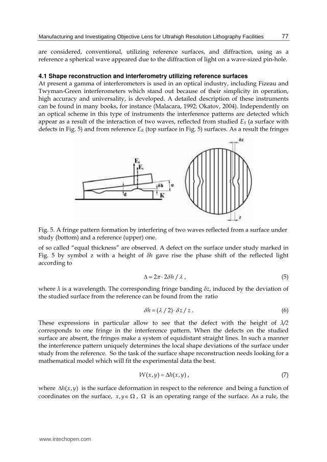
Manufacturing and Investigating Objective Lens for Ultrahigh Resolution Lithography Facilities
77
are considered conventional utilizing reference surfaces and diffraction using as a reference a spherical wave appeared due to the diffraction of light on a wave-sized pin-hole
41 Shape reconstruction and interferometry utilizing reference surfaces At present a gamma of interferometers is used in an optical industry including Fizeau and Twyman-Green interferometers which stand out because of their simplicity in operation high accuracy and universality is developed A detailed description of these instruments can be found in many books for instance (Malacara 1992 Okatov 2004) Independently on an optical scheme in this type of instruments the interference patterns are detected which appear as a result of the interaction of two waves reflected from studied ES (a surface with defects in Fig 5) and from reference ER (top surface in Fig 5) surfaces As a result the fringes
Fig 5 A fringe pattern formation by interfering of two waves reflected from a surface under study (bottom) and a reference (upper) one
of so called ldquoequal thicknessrdquo are observed A defect on the surface under study marked in Fig 5 by symbol z with a height of h gave rise the phase shift of the reflected light according to
2 2 hπ δ λΔ = sdot (5)
where λ is a wavelength The corresponding fringe banding z induced by the deviation of the studied surface from the reference can be found from the ratio
( 2) h z zδ λ δ= sdot (6)
These expressions in particular allow to see that the defect with the height of λ2 corresponds to one fringe in the interference pattern When the defects on the studied surface are absent the fringes make a system of equidistant straight lines In such a manner the interference pattern uniquely determines the local shape deviations of the surface under study from the reference So the task of the surface shape reconstruction needs looking for a mathematical model which will fit the experimental data the best
( ) ( )W x y h x y= Δ (7)
where ( )h x yΔ is the surface deformation in respect to the reference and being a function of coordinates on the surface x yisinΩ Ω is an operating range of the surface As a rule the
wwwintechopencom
Lithography
78
sought-for function (Braat 1987) is written in terms of some basis of functions and its description reduces to finding a set of the series coefficients ck
( ) ( )k kk
W c α=sumr r (8)
where r is a radius-vector of a point on the surface and ( )kα r is a set of basis functions Mostly common polynomials orthogonal on some area 0Ω are chosen as the basis For instance for the circular area these are Zernike polynomials which are widely used in optics (Rodionov 1974 Golberg 2001) The orthogonality of the polynomials results in the fact that each term of the series makes a contribution independent on the remaining terms into the mean-square of the wave front deformation Since the representation of the investigated function is global any local dilatation when approximating is smoothed thus distorting global view of the function Besides when reconstructing the surface shape it is important to evaluate not only the global surface shape but local errors too From this it follows that the mathematical model should be oriented on the description of the surface shape not only globally but locally too In the framework of this paper this dilemma was solved by introducing local deformations additionally to the global description (8) of the surface deformation function
0( ) ( ) ( )k k mj jk m j
W c cα β⎡ ⎤= + sdot minus⎢ ⎥⎢ ⎥⎣ ⎦sum sum sum mr r r r (9)
where cmj and j are coefficients and ldquospecialrdquo basis functions describe a m-th local deformation with the center in the point with the coordinate of r0m It is significant that the set of functions k(r) and j(r-r0m) are different in general case because the described function W(r) should not be interrupted in the range of definition It is the reason why the ldquospecialrdquo functions j(r-r0m) must be finite should not have discontinuity and their values at the definition range boundary must be equivalent to zero An algorithm of searching for the expansion coefficients of the surface model (9) was performed in two stages At the first stage the global surface shape error is approximated according to the (8) model At the second stage the residual local surface deformations are approximated by the right part of the expression (9) In our case the global description of the surface shape errors is performed with the help of Zernike polynomials WZ() and the residual local dilatations ndash by using the apparatus of local splines WS() which advantages when describing the optical surface deformations are analyzed in (Archer 1997 Sun et al 1998) in details
0 0 0 0
0 0
( ) ( ) ( ) ( )cos( ) ( )sin( )
( sin( )) ( cos( ))
Pz n Pz nm m
Z S nm n nm nn m n m
k k
i P j P ijS Si j
W W W c R m s R m
B B P
ρ ϕ ρ ϕ ρ ϕ ρ ϕ ρ ϕρ ϕ ρ ϕ
= = = =
= =
= + = + ++ sdot sdot sdot
sumsum sumsumsumsum (10)
where and are polar coordinates of the point on the surface cnm and snm are the expansion coefficients ( )m
nR ρ are radial Zernike polynomials BiPs is the basic function of the -spline of the order of pS on i-th interval of y coordinate and BjPs ndash is the basic function of the -spline of the order of pS on j-th interval of x coordinate and Pij corresponds to the
wwwintechopencom
Manufacturing and Investigating Objective Lens for Ultrahigh Resolution Lithography Facilities
79
points of control of the spline A number of works (Rodionov 1995 Swantner amp Weng 1994) are devoted to the methods for determining the coefficients of the mathematical model of the surface shape deformation function (10) by using interferometric data In present work algorithms and programs developed in (Gavrilin 2003) are used Currently available methods of digital registration and mathematical processing of interferograms allow reconstructing the surface shape (wave front aberrations) in respect to the reference surface Fig 5 with the accuracy up to 10000 where is an operating wavelength of the interferometer However the guaranteed surface shape accuracy of the reference in the root-mean-square (RMS) does not exceed 30 ndash 20 (Website Zygo 2009) that is two orders of magnitude worse than required for instance for projection nanolithography optics A substantially better situation is observed when studying surfaces at typical scales lower than 1 mm At these scales the accuracy of the reference surfaces is better than 1000 that allows measuring the surface shape deformations with the sub-nanometer accuracy On this basis a number of micro-interferometers with a digital fringe registration has been developed in the last few years (Blunt 2006 Chkhalo et al 2008 Website Veeco 2009 Website Zygo 2009) Below the spectrum of space wavelengths on the surface under study to be registered and where the surface shape measuring by interferometers with the sub-nanometer accuracy is limited by the lateral resolution of a microscope is given typically lies in the range of 03-1 microm
42 Interferometers with a diffraction reference wave The problem of conventional interferometers using the reference surfaces is solved by the application of interferometers with a diffraction wave as the reference proposed by VP Linnik in 1933 (Linnik 1933) The proposal is based on the theoretical fact that when a flat electromagnetic wave falls onto a pin-hole with a diameter comparable with a wavelength in an opaque screen consisting of a zero-thickness superconducting material diffracted behind the screen wave in a far wave zone is an ldquoidealrdquo sphere (Born amp Wolf 1973) This feature of the light diffraction was used as the basis for developing interferometers of this type The first interferometer attended to the investigation of optics with sub-nanometer accuracy for the EUV nanolithography has been made by GE Sommargren in 1996 As a source of the reference spherical wave he used a single-mode optical fiber with a core diameter (exit aperture) of about 4-5 microm The objective for a projection scheme of a EUV-nanolithographer was tested with the help of the interferometer (Sommargren 1996) The author evaluated the measurement precision in terms of the RMS at the level of 05 nm With a high-coherence laser the interferometer allowed testing a surface shape of individual optical elements The main disadvantage of the interferometer was a ldquobigrdquo source size A numerical aperture where the diffracted wave still remains ldquoan ideal sphererdquo is determined by expression NAref ltλd and in the case of λ=05 microm and d=5 microm corresponds to NAreflt01 Partly the low-aperture problem is solved at the expense of stitching measured data over different areas of the studied substrate or objective Along with the apparent loss of a measurement accuracy when using the stitching procedure there exists one even more serious disadvantage of using low-aperture interferometers associated with a strong irregularity of interferogram illumination Fig 6 demonstrates how the illumination irregularity results in error when determining the position of the fringe extremum In other words along with the apparent
wwwintechopencom
Lithography
80
loss of measurement accuracy connected with the stitching low-aperture interferometers have a significant systematical error induced by strong intensity anisotropy of the reference wave Therefore the recent trends are toward increasing the use of diffraction on man-made pin-holes in an opaque screen Modern microelectronic technologies provide manufacturing high-quality low-edge roughness pin-holes with diameters down to 40-50 nm
Fig 6 Shift of determined position of fringe maximum (systematic error) caused by the illumination irregularity
Such pin-holes are applied in diffraction interferometers operating at the working wavelength of a EUV nano-lithographer λ=135 nm which are installed on undulators of the last generation synchrotrons in USA and Japan (Naulleau et al 2000 Murakami et al 2003) An interferometer circuit installed on ALS (Berkeley USA) is given in Fig 7
Fig 7 Optical scheme of interferometer with diffraction reference wave installed on synchrotron ALS in Berkeley USA The picture is taken from (Medecki et al 1996)
The device operates in the following way The radiation falls onto a small pin-hole Gap installed on the lens object plane under study A diffracted ldquoidealrdquo spherical wave passing through the lens is distorted according to its aberrations and is collected in the image plane On the radiation way in-between the lens and the image plane a diffraction grating is installed which splits the wave-front into two ones corresponding to zero and to 1-st diffraction orders The zero-order radiation passes through the hole which diameter is big enough and exceeds a focusing spot thus preventing the distortion of the wave front The 1-st order beam is focused onto a small-size pin-hole Due to the diffraction behind the
wwwintechopencom
Manufacturing and Investigating Objective Lens for Ultrahigh Resolution Lithography Facilities
81
screen ldquoan idealrdquo spherical wave is generated The reference wave expands toward a CCD-camera where it interferes with a wave passed through the lens under test The measurement accuracy provided by the interferometer will be discussed later when comparing with our interferometer As we can see such interferometers are efficiently used for the final characterization of wave-front aberrations of objectives for EUV radiation At manufacturing stages of substrates and mirrors the producers of the optics usually use optical diffraction interferometers The experimental study of capabilities of point diffraction interferometers operating with a visible light has demonstrated a number of factors reducing the measurement accuracy Particularly systematic discrepancy of experimental data when studying the same optics with the help of visible and EUV light interferometers is observed (Goldberg et al 2002) All of this stimulated to study the way how finite conductance and thickness of the screen material have an effect on amplitude-phase characteristics of the diffracted wave behind the screen and correspondingly on the interferometer measurement accuracy In work (Chkhalo et al 2008) the calculations of the amplitude-phase characteristics of the diffracted field behind the screen in the far-field zone have been carried out They used the solution of a task about the field of a point source located above a half-space with arbitrary properties and covered with a film of any thickness and arbitrary optical constants given in (Dorofeyev et al 2003) Fig 8 illustrates the statement of the problem The diffraction of a flat wave on a circular hole with the radius of a in a film with thickness of hf and the inductivity of f in medias with parameters and 1 was considered The field was calculated behind the screen at Zgt0 on a spherical surface with a fixed radius R0=10 cm The radius R0 was chosen from practical reasons but its value does not produce any effect on the community of the result since the calculation was done for a case krgtgt1 where k=2λ is a wave vector of the diffracted wave in a point with the radius-vector r
Fig 8 Sketch of the geometry of the problem where hf is the thickness of the film heff is an effective film thickness (characterized by the skin-layer) d is the diameter of a hole 1 and f are the dielectric constants of the film and the medias θ1 and θ2 are the angles of diffraction Incident wave is schematically shown by the arrows
The results of the calculations as compared with the solution of classical task of diffraction on zero-thickness superconducting screen have shown that most real electrodynamical
wwwintechopencom
Lithography
82
characteristics of the screen material have an effect on phase characteristics of the diffracted field The calculation of the phase distortions was carried out for the films of aluminum molybdenum tungsten and a number of other materials The results of numerical calculations shown in Fig 9 represent a relative phase deviation on meridional angle of the diffracted scalar field in the case of aluminum different thickness films characterized by dielectric constant Alasymp-542-i218 at the wavelength 633 nm as compared with the case of a perfect screen |Al|rarrinfin The phase incursion ∆(θ) is expressed in nanometers The radius of the hole in the films was а=150 nm A case of free standing (=1=1) films was considered It is evident that the larger the meridional angle the larger is the phase deviation of the diffracted field in the case of a realistic screen We connect the result with an additional phase accumulation due to the field propagation through the real film at larger meridional angles (see Fig 8 for a qualitative clarification) We did not find a thickness dependence on the phase accumulation in the range of lthflt1000 nm where is a skin-layer because the phase can be effectively accumulated only inside the skin-layer The transitions hfrarr0 and |Al|rarrinfin |Al|rarrinfin or hfrarr0 led to the known textbook examples The corresponding diffraction fields for such idealized problems perfectly coincide with those of a spherical phase front
Fig 9 A relative phase deviation ∆(θ)=((0)-(θ))λ2 on meridional angle of the diffracted field in a case of Al different thickness film (Alasymp-542-i218) at the wavelength 633 nm on a spherical surface R0=10 cm the hole radius is а=150 せす
Other mechanisms of the phase distortion can be associated with the excitation of waveguide and surface modes in a plane layer and with a diffraction of such modes by a hole followed by their radiative decay Since the dielectric constant of all materials in soft X-ray and EUV ranges are close to unity Re()asymp1 corresponding phase distortions are minimal It is one of the reasons why the quality of the diffracted reference wave in EUV region has a better result in a higher measurement precision The carried out calculations have shown (see Fig 10) that the angular dependencies of the phase distortions on the meridional angle weakly change for different materials The only exception is osmium for which the phase deformation was extremely low Optical constants of materials used in these calculations were taken from (Palik 1985)
wwwintechopencom
Manufacturing and Investigating Objective Lens for Ultrahigh Resolution Lithography Facilities
83
Fig 10 Angular dependencies of the phase distortions on the meridional angle for different materials
By this means a fundamental limitation of the point diffraction interferometer measurement accuracy is caused by the aberrations of the reference spherical wave induced by the interaction and propagation of secondary waves through the screen material These aberrations are liable to reach a few nanometers depending on the angular aperture If we take into account the polarization characteristics of the light the aberration of the reference wave increases a few times depending on azimuth angle (Dorofeev 2009) The quality of a diffracted wave strongly depends on wave aberrations of preliminary optics focusing the laser beam and the accuracy of adjusting the laser beam axis in respect to the pin-hole center (Otaki et al 2002) All these limit the working aperture of the interferometer and result in the necessity of testing high-aperture optics zones The following stitching procedure of the zonal data raises additional errors All of these disadvantages hinder to widespread use of the point diffraction interferometers in an industry Taking into account all of these problems and limitations the problem of searching for alternative and more perfect methods for the spherical wave generation becomes very urgent
5 Spherical wave source on the basis of tipped fiber
The sources of the spherical wave based on tipped down to a sub-wave exit aperture of the single mode fibers are free from the many of mentioned above problems The application of such fibers as a reference spherical wave source for the point diffraction interferometers has been proposed in (Klimov et al 2008) In Ref (Chkhalo et al 2008) the aberrations of the wave generated by the sources at the wavelength of He-Ne laser =633 nm have been studied These investigations have demonstrated a number of advantages of spherical wave sources as compared with the conventional ones based on a pin-hole in an opaque screen One of the advantages is connected with the fact that in the optical fiber the eigenmodes are excited and correspondingly the quality of the diffracted wave does not depend on aberrations and the mechanical adjustment of the preliminary optics A high degree of homogeneity of the diffracted wave (dgt1) is combined with a high intensity because the light is input into the fiber using high-efficiency methods through a 5-
wwwintechopencom
Lithography
84
microm-diameter core The convex shape of the source Fig 11 decreases the ldquotiprdquo effect bound to the interaction of the off-axis rays with a metallized part of the fiber along the perimeter of the exit aperture The lack of a flat screen around the source significantly decreases diffracted wave distortions connected with the light polarization The well developed methods for handling optical fibers make it possible to easily control the polarization parameters of the diffracted radiation and implement various schemes for interference measurements For instance two or even more coherent sources can be organized with the given polarization of each other
Fig 11 Photographs of the fiber based source taken with scanning electron microscope (marked as a) and b)) and the source with on optical connector
The quality of the diffracted wave of the tipped fiber based source was studied with an interferometer (Kluenkov et al 2008) at two wavelengths =633 nm (He-Ne laser) and =530 nm (second harmonic of Nd-YAG laser) As opposed to the former experiments when in the measurement scheme an optical observation system collected the interfering fronts onto the CCD-camera in present work the data obtained by the direct detection of the fronts on the window-free CCD-camera are given As the experiments showed both the observation systems and even a thin glass window introduce a significant at the level of parts of nanometer error into the measurements
Fig 12 Experimental setup for studying the wave front deformations of the tipped fiber based sources of spherical wave 1 is a laser 2 is a system for input the light into the fiber 3 is a single mode fiber optics coupler 4 is a polarization controller 5 are sources under study 6 is a CCD-camera and 7 is a computer
wwwintechopencom
Manufacturing and Investigating Objective Lens for Ultrahigh Resolution Lithography Facilities
85
The new experimental setup is given in Fig 12 Polarization controllers (item 4 in Fig 12) allow to transform an elliptical polarization of the light at the output of the sources into a linear one as well as to superpose the polarization planes which provide the best contrast of the interference pattern The distance between the sources determining the fringe number (a wedge between two interfering wave fronts) was varied in the range of 1-10 m The measurements were carried out for different angles between the source axes The numerical aperture was varied by approaching (moving off) the CCD camera in respect to the sources A typical interferogram and a wave aberration map obtained in the experiments are shown in Fig 13 The operating wavelength was =530 nm
Fig 13 A typical interferogramm and a wave aberration map observed in the experiments obtained at a wavelength =530 nm
The measured dependencies of the wave deformation RMS on numerical aperture NA of this couple of sources are given in Fig 14 The pictures correspond to the measurements in small (left) and in large (right) numerical apertures Left graphs on both pictures correspond to the experimental data The data obtained with the interferometer installed on the synchrotron ALS in Berkeley USA are marked by stars The interferometer using a pin-hole in an opaque screen as a reference spherical wave source operates at the wavelength =135 nm and is considered as a reference for the measurement accuracy among the point diffraction interferometers (Naulleau et al 1999) It is clearly seen from the pictures that wave front aberrations of the source developed in this work are even less as compared with the ALS-sources despite a longer operating wavelength When analyzing the obtained experimental data there is a need to pay attention to two facts bull Relatively ldquohighrdquo of order λ1000 total aberration of the diffracted waves is observed
at large numerical apertures (NAasymp03) bull Regular structure (symmetry) of the wave front deformation map is clearly seen Such maps and statistical values of the deformations are practically found for all couples of so called ldquohigh qualityrdquo sources The wedge direction between interfering fronts (a line passing through the sources) represents itself as the axis of the symmetry Particularly the deformation map can be put ldquohorizontallyrdquo by turning the wedge through 90 degrees All of this points to the presence of an aberration caused by some kind of physical reason rather than by technological fluctuations This aberration rises with the increase of the observation angle just as it is shown in Figs 9 and 10 In case of understanding the physical nature of this aberration it can be taken into account when reconstructing the true wave deformation (surface shape) that results in increasing the working aperture of the interferometer by a few times
wwwintechopencom
Lithography
86
Fig 14 Averaged over 9 measurements total wave front deformations of couple of the fiber based spherical wave sources depending on numerical aperture (left graphs in both pictures) and ALS-data (Naulleau et al 1999) (stars) Working wavelength is =530 nm First picture corresponds to lower and right ndash to the higher numerical apertures The right graphs in the pictures are corrected according to the geometry of the experiment
This fact of the uniform angular dependence of the aberration let us interpret in a new manner the measurement data obtained in ALS and in our experiments In the Youngrsquos experiment carried out in ALS the least distorted parts of the diffracted waves round their own axes interfere Correspondingly RMS of the aberration is calculated over the range of the cone limited by the numerical aperture NA Opposite to that in our case side parts of the wave fronts interfere Fig 12 in the range from zero degree up to a double value of the angular aperture of the wave front In other words in the search for the wave front aberration RMS the averaging is performed over a double numerical aperture 2NA Therefore the measured dependences presented in Fig 14 (left graphs) can be corrected in the manner as it is shown by arrows (right graphs) As it is seen from the picture the source of the reference spherical wave based on a tipped single mode fiber has a substantially lower wave front aberration and a higher working aperture as compared with the conventional one based on pin-hole in an opaque screen
6 Diffraction interferometer based on a single mode fiber with the sub-wave exit aperture
On the basis of a tipped fiber source of the reference spherical wave the laboratory sample of an interferometer has been developed and manufactured which optical scheme and photo are presented in Figs 15 and 16 The interferometer is installed in a basement thermostated room on a bearer separated from the house footing For the additional protection against vibrations the instrument is installed on 12 bellows under 16 bar pressure Since the measurement accuracy is extremely high the turbulent air flowing inside the interferometer and effecting optical paths along the rays can introduce additional errors To solve these problems the interferometer is placed into a vacuum chamber which is pumped out down to a pressure of 1 Pa
wwwintechopencom
Manufacturing and Investigating Objective Lens for Ultrahigh Resolution Lithography Facilities
87
Fig 15 Optical scheme of the interferometer 1 ndash PC 2 ndash registering system 3 ndash observing system 4 ndash source of spherical wave 5 ndash flat sharp-edge mirror 6 ndash three-axes-controlled precision bench 7 ndash tested concave surface 8 ndash single mode optical fiber 9 ndash polarization controller 10 ndash laser
Fig 16 Photograph of the vertical vacuum interferometer
wwwintechopencom
Lithography
88
The optical scheme shown in Fig 15 corresponds to the interferometer for studying concave spherical or weakly aspherical surfaces The spherical wave source (item 4 Fig 15) is mounted on a high-precision three-axis-controlled bench (item 6 Fig 15) in the direct in a distance of several micrometers proximity from the flat mirror (item 5 Fig 15) The reference spherical wave which after reflecting from the studied surface (item 7 Fig 15) carries the information about its form is focused on a flat mirror and being reflected from it goes into the CCD registering system where it interferes with a part of the reference front directly propagating to the detector The main disadvantage of this scheme is connected with the fact that the investigated sample is irradiated by the most distorted side part of the wave front that practically halves the interferometer operating numerical aperture For solution of this problem in (Kluenkov et al 2008) the scheme of the interferometer with two low-coherent sources of the reference spherical waves has been proposed (Fig 17) In this scheme one source forms the spherical wave laquoSpherical wave 1raquo irradiating the investigated surface while the spherical wave of the second source laquoSpherical wave 2raquo is directed into the registering system The radiation reflected from the investigated surface contains the information on its shape and after reflecting from the flat mirror is directed to the registering system where interferes with the reference laquoSpherical wave 2raquo The main advantage of the scheme is that the axes of the wave fronts coincide with the axes of the investigated surface and the registering system which provides the minimal deformations of reference fronts
Fig 17 Scheme of the low-coherence diffraction interferometer with two sources of the reference spherical wave
As a source of the radiation a super-luminescent diode with a coherence length about 20 microns is applied It prevents parasitic interferences of wave fronts produced by different elements of the optical scheme For observing the correct interference the optical path of the light of source 2 is increased by a double distance from the investigated surface to the sources In this case the interference is observed only for the noted above wave fronts The radiation of the source 1 directly going into the registering system creates only a background signal on the detector
wwwintechopencom
Manufacturing and Investigating Objective Lens for Ultrahigh Resolution Lithography Facilities
89
As it was already marked in diffraction interferometers a divergent spherical wave is used as a reference wave It imposes a number of restrictions on the interferometer capabilities Strictly speaking with their help it is possible to investigate only concave spherical and slightly aspherical surfaces and objectives The measurement of the form of strongly aspherical concave or even spherical but convex surfaces demands using additional optical elements transforming the reference divergent spherical wave to a new one which front is close to the surface shape under study Of special interest are interferometric measurements of objective wave front deformations for example for final certification of the objective wave aberrations or for objective adjustment directly in an interferometer or in the case of the objective application for studying convex spherical surfaces In Fig 18 the scheme and photograph of measurements of six-lens objective in the interferometer are shown In this scheme two coherent sources are used The measured data of the wave deformation were PV = 423 nm and RMS = 82 nm
Fig 18 Scheme of the interferometer with two coherent sources of the reference spherical wave (left) and photograph in the interferometer (right) for testing sixs-lens objective 1 ndash PC 2 ndash registering system 3 ndash observing system 4 ndash source of spherical wave 5 ndash flat sharp-edge mirror 6 ndash three-axes-controlled precision bench 8 ndash single mode optical fiber 9 ndash polarization controller 10 ndash laser 11 ndash studied objective
The certified objective was used for the interferometric measurement (Fig 19) of a convex spherical surface of a special compensator which in turn later on was applied for studying the concave ashpherical surface for a double-mirror objective For reconstructing the true shape of the convex surface the expansion coefficients at basis polynomials corresponding to the objective aberrations were deducted from the measured ones Aspherical surfaces are used in the majority of high-resolution optical objectives in order to widen the field of view of the optical systems Direct testing of aspherical surfaces by using an interferometer with the spherical reference wave is often difficult or even impossible For example Fig 20 a) shows the interferogram for a concave aspherical substrate with about 7-microm deviation of the surface from the nearest sphere The measurements were carried out by using the basic scheme shown in Fig 15 It is evident that a large number of fringes makes
wwwintechopencom
Lithography
90
the position determination of the minima almost impossible Moreover the upper part of the interferogram is simply not there which is explained by a large about 100 microm diameter of the focusing spot for which the beam partially propagates above the edge of mirror (item 5 Fig 15) and misses the measurement system
Fig 19 Optical scheme (left) and photograph of units (right) in the interferometer for certification of convex surfaces Designations on the scheme are the same as in Fig 15
Fig 20 Interferograms from the aspherical concave mirror М2 obtained without wave-front corrector (a) and using corrector (b)
One of the most effective solution of this problem is the use of wave-front correctors ie special optical elements that transform a reference spherical wave front into an aspherical one which shape is identical to the shape of the studied surface In order to take into account the wave-front distortions due to errors of the corrector itself its surfaces should be only spherical In this case it is possible to test these surfaces with subnanometer accuracy by using a spherical reference wave interferometer by the techniques stated above The scheme for testing the concave aspherical surface by using a corrector is presented in Fig 21 The parameters of the corrector suitable for testing the concave aspherical surface
wwwintechopencom
Manufacturing and Investigating Objective Lens for Ultrahigh Resolution Lithography Facilities
91
ie radii of the surfaces thickness and the distance from the reference wave source to the top of the first surface were calculated by minimizing the difference of longitudinal aberrations of the tested aspherical surface and the corrector described in (Malacara 1992 Puryaev 1976) in detail The calculated root-mean-square deviation of the wave front after the corrector from the investigated aspherical shape was RMS=λ1810 This suffices for testing the mirror surface of a nanolithographer with a double-mirror objective It is clearly seen from Fig 20 b) that the interferogram from the aspherical surface obtained by using such a corrector can be reliably processed
Fig 21 Optical scheme (left) and photograph of units in interferometer (right) for certification of concave aspherical surfaces using corrector 1 - computer 2 - registering system 3 - observation system 4 - spherical wave source 5 - flat mirror 6 - 3D precision table 7 - investigated concave aspherical surface 8 - optical fiber 9 - polarization controller 10 - laser 11 - corrector
The analysis of the influence of misalignment in the measurement optical scheme and a thickness error of the compensator on ldquoasphericityrdquo of the wave-front passing through the corrector and accordingly on the measurement accuracy has shown that the requirements for these characteristics of the optical scheme are easily performed in practice In particular the error of a compensator thickness within the limits of plusmn01 mm leads to a wave front aberration at the level of λ1000 Studying of the convex aspherical surfaces is complicated by the fact that besides the corresponding transformation of a spherical front into an aspherical one the corrector must provide a converging front of the wave All of these essentially complicate both the calculation and the design of the corrector In particular in some cases it is necessary to use aspherical surfaces or more than one lens In the case of optics for Schwarzschild objectives this problem is solved easily enough As a corrector the mating concave aspherical mirror which surface has been preliminary tested by using the corrector system described above and corrected according to the procedure described in the next section can be used The measurement scheme is presented in Fig 22 This scheme can be applied for the final
wwwintechopencom
Lithography
92
adjustment and certifications of the objective It is noteworthy to mention that this method can be applied for a convex spherical surface characterization too besides using additional objectives as it is shown in Fig 19
Fig 22 Measurement scheme of aspherical convex mirror М1 using mirror M2 as a wave-front corrector 1 - computer 2 ndash CCD camera 4 - spherical wave source 9-polarization controller 10 ndash laser 11 ndash Schwarzschild objective М1 and М2 ndash convex and concave aspherical mirrors
The measurement accuracy provided by the interferometer depends on many factors including the quality of the reference-wave source the accuracy of determining the positions and a number of interference minima and the accuracy of mathematical retrieval of the surface (wave-front) shape using a limited number of experimental points and the number and degree of the polynomials In turn the accuracy of determining the minimum positions is strongly dependent on the width of the interference pattern the degree of pollution of the interference pattern by ldquoparasiticrdquo interference the method of its rejection the uniformity and intensity of the interfering fronts and a number of other unmanageable factors In this work the interferometer measurement precision was evaluated by studying the rotations of the measured surface maps corresponding to the physical turn of the tested detail The idea of this method is the following If the interferometer provides zero-error measurements then when the detail is rotated the measured surface map should turn correspondingly and the measured statistical parameters of the surface shape deformations should remain unchanged The measured surface deformation maps of a spherical substrate with a numerical aperture NA=014 corresponding to different rotations of the detail are
wwwintechopencom
Manufacturing and Investigating Objective Lens for Ultrahigh Resolution Lithography Facilities
93
presented in Fig 23 The figures demonstrate that the turn of the maps is well observed and the statistical parameters of the deformations change within the limits of RMS=307plusmn0055 nm This test confirms the high measurement accuracy provided by the interferometer which is sufficient for many lithographic applications
Fig 23 Maps and statistical parameters of the surface form deformation corresponding to rotations of the spherical mirror by 0 90 180 and 270 degrees
To summarize this section it is possible to ascertain that the developed interferometer with the diffraction reference wave provides a precision certification of the high-aperture optical surfaces and systems to the subnanometer accuracy
7 Shape correction of optical surfaces to subnanometer accuracy
The developed precise techniques for measuring the shape of optical surfaces made it possible to pass to the main stage the correction of the surface shape made with traditional accuracy λ2 - λ20 depending on the type of optics up to λ1000 - λ2000 In the context of the given work two methods of correction have been developed a vacuum deposition of thin film coatings and ion etching of previously deposited films through metal masks An extremely high accuracy of correcting the surface shape imposes specific requirements on the correction method 1 As a result of the correction process the microroughness of the corrected surface (as a
rule it is initially supersmooth) should remain at the initial level
wwwintechopencom
Lithography
94
2 In the case of a shape correction by means of a local thin film deposition the correcting layers should not distort the substrate surface shape due to intrinsic stress ie they should have a minimally possible stress
3 The correction method should provide the deposition or the removal of materials in a wide range of thickness (1-300 nm) with the accuracy not worse than several percents This problem is especially urgent in the last correction stages when the thickness of the layers to be deposited (removed) is about one nanometer
4 The film materials should allow their complete removal from the substrate (for example chemically) without changing the initial surface shape and microroughness It allows repeating the correction process in the case when the previous correction attempt failed
Researches on stress compensation in multilayer structures and on a substrate restoration have shown that a material meeting all these requirements is CrSc multilayer structure (Salashchenko 2001) The deposition of coatings was made by the magnetron sputtering method The scheme of the correction process and the photograph of the installation are shown in Fig 24 Vacuum in the chamber was (07-1)middot10-6 Tor pressure of working gas (argon) was (07-09)middot10-4 Tor The characteristic power on DC magnetrons was 300-400 W The film thickness control of the deposited layers is performed by variating the passage speed of the corrected surface above the magnetrons sources The stabilization of the discharge power and the argon pressure were provided at the level of 01 The predetermined distribution of the layer thickness over the substrate surface was reached due to the application of figured diaphragms mounted between the magnetron sources and the substrate In addition the substrate rotates around its axis Local values of the film thicknesses over the substrates were measured with an x-ray reflectometer at 447 nm wavelength The details of these measurements will be shown below
Fig 24 Photograph of a technological facility and scheme of surface shape correction by means of multilayer film deposition through masks
The operational experience with this technology has shown a number of important advantages Firstly the roughness of the film surface practically does not depend on the angle of incidence of the atoms in respect to the substrate that allows to carry out the
wwwintechopencom
Manufacturing and Investigating Objective Lens for Ultrahigh Resolution Lithography Facilities
95
correction procedure at normal angles It reduces shadows on the surface increasing the localness of the correction correspondingly Secondly the high accuracy of the layer thickness control up to 1 provides a high reproducibility of the process The film-correction method proved to be efficient for initial stages in which the layers with of tens-hundreds nanometers are deposited in a single correction The process becomes unstable as the thickness of deposited layers decreases down to the units of nanometers Correcting films have changed the proper color that is connected with films oxidation at initial stages of deposition The distribution of oxygen in depth of scandium film obtained with the help of a secondary ion mass-spectroscopy (Drozdov et al 2009) is given in Fig 25 The figure shows an increased content of oxygen on the film surface and at the film-substrate interface Other serious disadvantages of the thin-film-correction method has a discrete and iterative character of the process After each iteration it is necessary to vent the vacuum chamber to make a new diaphragm to pump the chamber again All this strongly decreases the throughput of the process
Fig 25 The distribution of oxygen in depth of scandium film deposited onto Si-substrate
Therefore the application of ion-beam etching at the final correction stage looks very attractive This method allows in particular when focused ion-beams are used to realize the ldquomasklessrdquo correction without frequent opening of the installation to atmosphere Now this method is widely used for substrate form correcting and even for final ion-beam polishing in optical industry (Allen et al 1991 Chason amp Mayer 1993 Ghigo et al 2007) Recently an intensive literature has evolved which is devoted to the application of this method for the precision correction of substrates for projection EUV lithography (Dinger et al 2000 Murakami 2007) For the ion beams applied for the surface shape correction of substrates for EUV and soft X-ray optical elements a number of requirements are imposed the basic of which is the preservation of the surface roughness at an initial (supersmooth) level even when the removed layer depth reaches a few hundreds of nanometers Therefore an optimization of ion energy and incidence angles of the ions on the corrected surface at different depths of material removal is an actual problem Other problems inviting a further investigation are connected with some features of the ion-beam etching at an extremely small depth (asymp 1 nm) removal of materials The experiments have been performed on the installation (Fig 26) with the Cauphmanraquo type ion-beam source KLAN-103M (Website Platar Company 2009) The basic advantage of
wwwintechopencom
Lithography
96
this source is the possibility of working with small ion energies Еi = 50- 300 eV at a significant current density
Fig 26 Photographs of installation for substrates surface shape correction by ion-beam etching
The main characteristics of the ion source are the operating gas is argon or other inert gases the maximal diameter of the ion beam is 100 mm the maximal ion current is 100 mA the maximal ion current density is up to 23 mAcm2 the range of ion energy regulation is 50-1500 eV at the energy spread of plusmn3 eV the discharge working voltage is 35-50 V the thermo-cathode is made of thoriated tungsten (03 mm in diameter) filament Presence of charge-neutralizer (additional thermo-cathode) allows compensating the ion beam charge that provides using the ion source for correction substrates of dielectric materials too The measured dependence of the etching rate of CrSc coating on the removal depth taken at ion energy Еi=200 eV and grazing incidence angle of θ = 42ordm is shown in Fig 27 by dots It is evident that at the initial stage of the etching the removal is less than 120 nm practically a linear increase of the etching rate from the removal depth is observed At a very small etching depth h lt10 nm a wide scatter of the etching rate values is observed Considering the data of the secondary ion mass-spectrometry Fig 28 such a behavior of the etching rate can be explained by oxidation of the sample surface The etching rate of the oxide layer is significantly lower as compared with pure CrSc material If take this into account the calculated etching rate a solid line in Fig 27 matches well the experimental data The observed instability of the etching rate at h lt10 nm might be explained by the variation of the oxidized layer depth in various samples When samples were etched by a neutralized beam (stars in Fig 27) no changes of the rate were observed With the increased ion energy up to 300 eV Fig 29 such instability of the etching rate is not observed either According to atomic-force microscopy measurements the surface roughness remained constant at the level of 02 nm down to 400 nm removal depths For the ion energy of Еi=300 eV when the etching depth exceeds 80 nm an increase of surface roughness is observed (Fig 30)
wwwintechopencom
Manufacturing and Investigating Objective Lens for Ultrahigh Resolution Lithography Facilities
97
Fig 27 Dependence of etching rate on removal depth of CrSc multilayer structures dots are experiment with ions stars are experiment with neutrals and line is calculation accounting etching of the oxidized layer Ion energy Еi = 200 eV and current Ii=60 mA
0 5 10 15 20 25 30 35 40 4500
40x104
80x104
12x105
16x105
Oxigen
SIM
S in
ten
sit
y a
u
Depth nm
Fig 28 Typical distribution of oxygen atoms on depth of CrSc multilayer structure taken by secondary ion mass-spectrometry
The dependences of etching depth on an ion dose (the dose is the product of ion current and etching time) both from the ion current at fixed time and from the time at fixed current show a good linearity that is useful from the practical point of view because it allows to easily define the necessary etching time at a given ion current The example of the dependences of the etching depth on the dose is given in Fig 31 The dashed line corresponds to the linear approximation of the dependence and line with squares represents the experimental data It should be noted that the experiments carried out with greater ion energies up to Ei=15 keV have shown a fast growth of the surface roughness even at small nearby 20ordm grazing angles of incidence of the ions on the surfaces (Chkhalo et al 2008)
wwwintechopencom
Lithography
98
Fig 29 Dependence of ion etching rate on etching depth of CrSc multilayer structures at ion energy Еi = 300 eV (area of small removal depths)
Fig 30 Dependence of surface roughness of CrSc multilayer structures on etching depth at sputtering by argon ions with energy Еi = 300 eV
Fig 31 Dependence of etching depth of the CrSc multilayer structures on ions doze at ion energy Еi = 300 eV - - - linear approximation of the dependence
0 20 40 60 80 1000
10
20
30
40
Etc
hin
g d
ep
th n
m
Dosage mAmin
wwwintechopencom
Manufacturing and Investigating Objective Lens for Ultrahigh Resolution Lithography Facilities
99
For correcting the surface shape of substrates for imaging X-ray optics when the subnanometer form accuracy is required the following strategy providing minimal time expenses has been chosen At the initial stage when peak-to-valley values (P-V) of the surface shape are 50-200 nm the local deposition of the thin films is applied Then at the reduction of the P-V values down to 10-20 nm the ion beams with the energy of 200 eV are used At the final correction stage the 300 eV-ions are applied Figure 32 illustrates the result of using this correction procedure for a spherical substrate with a numerical aperture of NA=025 (the diameter is 130 mm and the curvature radius is 260 mm) which was initially the standard etalon for a conventional interferometer The initial surface map is shown in Fig 32 a) The parameters of the surface were P-V=426 nm and RMS=73 nm The surface shape improved to P-V=73 nm and RMS=06 nm (Fig 32 b)) Thus a root-mean-square deviation of the initial surface shape from an ideal sphere has decreased in 12 times ie in units of the interferometer working wavelength (=0633 microm) it has became better than λ1000 The photograph of this mirror mounted on a metal frame is given in Fig 33
Fig 32 Maps of deviations of the spherical surface shape from the nearest ideal sphere a) initial shape (P-V=426 nm RMS=73 nm) b) after 12-th correction (P-V=73 nm RMS=06 nm)
Fig 33 Photograph of the multilayer spherical mirror for 135 nm wavelength in the frame Diameter of the working aperture is 130 mm
wwwintechopencom
Lithography
100
In spite of a greater wavelength of the traditional deep ultraviolet lithography (193 nm) because of a great number of lens and high requirements for the quality of the projective objectives the methods of correction and certification with a subnanometer accuracy described in this article are urgent for the refracting optics too In connection with this the researches on etching of fused quartz surfaces by ion beams with a compensated charge have been carried out As well as in the case of metal surfaces the main attention was given to the etching rate to the reproducibility of the etching process and to the surface microroughness depending on the beam characteristics incidence angles and material removal depths In Fig 34 the dependences of quartz etching depth on the etching dose are presented The dashed lines in the figure correspond to linear approximations of the dependencies The ion energy was 200 and 300 eV the grazing incidence angle was 42ordm The comparison with similar dependences for CrSc Fig 31 shows that the etching rate of fused quartz is almost twice as much No nonlinearity at the initial stage of the etching is observed that on the one hand proves the hypothesis about the effect of the oxide layer in the case of CrSc material and on the other hand essentially facilitates the correction process
0 100 200 300 4000
50
100
150
200
250
300
350
Etc
hin
g d
ep
th n
m
Dosage mAmin
Fig 34 Dependences of the etching depth on the doze for fused quartz Etching is performed by argon ions with compensated charge and with energy Еi = 200 and 300 eV - - - - linear approximation of dependences
The data on the surface roughness of a fused quartz substrate etched by ions (neutrals) with energies of 200 and 300 eV for various removal depths measured by means of the atomic-force microscope and by x-ray diffractometry are presented in table 1 The substrates manufactured by General optics (USA) were used in the experiment The minimal roughness of initial surfaces measured with an atomic-force microscope was 013 nm and with the x-ray reflection it was about 04 nm From the table it is evident that atomic-force microscope measurements have shown a weaker influence of the etching process on the surface roughness in comparison with the roughness measurements made by the x-ray diffractometry method A more detailed discussion of this difference is beyond the given article Thus the presented experimental data show that these technologies of vacuum deposition and ion-beam etching in the aggregate allow to correct with a subnanometer accuracy the surface shape of optical elements practically of any materials (metals dielectrics semiconductors) with keeping the surface on a supersmooth level This technology is
wwwintechopencom
Manufacturing and Investigating Objective Lens for Ultrahigh Resolution Lithography Facilities
101
suitable for manufacturing elements for imaging x-ray optics and for high resolution systems in visible and deep ultra-violet ranges
Table 1 Roughness of fused quartz substrates depending on neutral (ion) energy and etching depths measured by atomic-force microscopy (AFM) and x-ray diffractometry (X-ray) methods
8 Reflecting multilayer interference mirrors
The final stage of manufacturing a precise mirror for ultrahigh resolution imaging x-ray optical systems is the procedure of the deposition of multilayer reflecting coating on a substrate A low polarizability of materials (le1) and correspondingly a small jump of the refraction factor Δn=00001-01 on the vacuum-material interface and a strong absorption of the radiation by all materials completely exclude the application of refractive optics in the extreme ultra-violet and soft x-ray ranges Because of a low reflection from one interface the reflection optics of normal incidence can be only interferential and the number of layers demanded for the achievement of a high reflectivity depending on a wavelength can reach a value of 102-103 The absorption of the radiation in multilayer structures leads to the fact that the reflectivity is always less than unity While choosing an optimal pair of materials providing a maximal reflectivity on a given wavelength the circumstance is often used that in the range of wavelengths directly adjoining the absorption edge of the material gt AE (AE is the wavelength of the material absorption edge) and coinciding with an anomalous dispersion of the optical constants the lowest absorption and the maximal polarizability of materials are observed For some materials in the field of K-and L- absorption edges the refraction factor can even exceed unity In Fig 35 the calculated spectral dependences of the maximal reflection coefficients for the most attractive pairs of materials in a spectral range of 3 - 16 nm representing the biggest interest for projection nanolithography and high resolution x-ray microscopy are shown The greatest experimental reflectivity about 70 was obtained at a wavelength of 135 nm The spectral range around λasymp67 nm (area of boron anomalous dispersion) is of interest for projection x-ray lithography However the reflectivity obtained here with LaB4C multilayer mirrors at a normal angle of incidence does not exceed 45-47 (Andreev et al 2009) that is not enough for lithographic applications
wwwintechopencom
Lithography
102
2 3 4 5 6 7 8 9 10 11 12 13 14 15 1600
01
02
03
04
05
06
07
08
CrSc
CrC
LaB
MoBe
MoSi
experiment
Refle
ctivity
Wavelength nm
Fig 35 Calculated (lines with symbols) and experimental (stars (Website ESRF 2006 Andreev et al 2003)) reflection coefficients of mostly attractive pairs of materials in X-ray and EUV ranges
On the short-wave length side the working wavelength of the normal incidence multilayer optics is limited by technology capabilities for depositing high-quality short period multilayer structures At present the shortest periods have multilayer structures based on WB4C (the period dasymp1 nm) (Vainer et al 2006 Platonov 2002) and CrSc (dasymp15 nm) (Salashchenko amp Shamov 1997 Website ESRF 2006) A number of special requirements are imposed on the multilayers which should be deposited onto substrates for imaging optics In particular to provide a constructive interference of the waves reflected from different interfaces the radiation wavelength λ the local angle of incidence ( )rθ f
and the period of the multilayer structure ( )d rf should satisfy
the Bragg condition
( )2sin ( )
d rr
λθ=f
f (11)
where rf is a radius-vector of a point of incidence of the radiation on the structure As the
incidence angles are a function of the coordinates it results in the necessity to deposit multilayer structures with a variable over the surface period so-called ldquogradedrdquo structures In some cases for example when the angular divergence of the X-ray beam falling on one point of the mirror surface exceeds the Braggrsquos peak width the multilayer structure should have a variable period on depth (Kozhevnikov et al 2001) One more important feature of multilayer structures for precise optics can be explained as follows For multilayer dispersive elements the maximum deviation of the local value of the period d from the nominal one is determined by the condition of synchronism of the waves reflected from various interfaces which can be expressed through the spectral selectivity of a mirror 1 S d d Nδλ λ δ= = cong (N is a number of periods) In the case of precision multilayer imaging optics when the required surface shape accuracy is at a subnanometer
wwwintechopencom
Manufacturing and Investigating Objective Lens for Ultrahigh Resolution Lithography Facilities
103
level to the synchronism condition an extra requirement for the preservation of the mirror surface shape is added For example for the well-known MoSi multilayer structure optimized on the wavelength of λ=135 nm the period is dasymp7 nm at a number of periods N asymp 40 Correspondingly the general thickness of the structure is L=Nd=280 nm The local error of the period of 1 will affect weakly on reflectivity however the surface shape of the mirror will produce a change of 28 nm which already can essentially produce an influence on imaging properties of the mirror From these simple estimations two important conclusions follow Firstly when designing and manufacturing the surface shape of a substrate it is necessary to take into account the real thickness of a multilayer coating which would be deposited onto the substrate Secondly it is necessary to provide a high at a level of 02-03 accuracy of local values of the period over the mirror surface Besides an intrinsic stress in the multilayer structures which can also deform the surface shape must be taken into account The estimation of the deformation x of a substrate with a diameter D a thickness hsub with the Yung modulus E and the Poisson factor ν on which a hf thick film with the intrinsic stress σ is deposited can be performed by means of equations
2
2
3
4
1
f
sub
h Dx
Y h
EY
σδ
ν
sdot sdot= sdotsdot= minus
(12)
For instance for optimized on maximum of the reflection coefficient MoSi multilayer structure (portion of Mo layer in the period =dMo(dMo+dSi) = 04) the stress in our case is about σ =-350 М『а (Fig 36) At deposition of such a multilayer structure (general thickness is L=Nd=280 nm) on a substrate of fused quartz with the diameter D=220 mm and thickness h=50 mm (Y=844 》а) the maximal deformation of the substrate surface would be about 17 nm that essentially exceeds an admissible level of the surface shape deformation of a mirror for EUV lithography Different groups solve this problem in different ways One the solution is the use of mirrors with a specified thickness ratio of molybdenum layer in the periods Mo asymp 05 - 07 when the stress is close to zero (Windt et al 1994 Zoethout et al 2003) The other solution consists in adding a third material into the periods for example Ru (Oshino et al 2003) However all these methods either because of a stronger absorption of EUV radiation or because of an interface roughness growth have smaller of 10-20 absolute values of the reflectivity In IPM RAS a technique of the stress compensation based on the use of special sublayers lying under the basic MoSi multilayer structure is under development For CrSc multilayer structures the stress is close to zero at γCr=dCr(dCr+dSc)asymp05 (Fig 37 (Andreev et al 2005)) At γCrgt05 a sign of the stress is positive on the contrary to the MoSi structures at γMo= 04 when it is negative The total stress σeff in the structure consisting of CrSc and MoSi multilayer films can be determined from a ratio
( ) ( )
( ) ( )Mo Si Mo Si Mo Si Cr Sc Cr Sc Cr Sc
eff
Mo Si Mo Si Cr Sc Cr Sc
d N d N
d N d N
σ σσ ⎡ ⎤sdot sdot + sdot sdot⎣ ⎦= sdot + sdot (13)
from which it follows that optimizing the composition and the thickness of CrSc layers it is possible to compensate the stress in the basic MoSi reflecting multilayer structure
wwwintechopencom
Lithography
104
Fig 36 Stress in MoSi multilayer structures depending on ratio of Mo layer in period γMo=dMo(dMo+dSi) at fixed period d=697 nm
Fig 37 Stress in CrSc multilayer structure depending on ratio of Cr layer in period γCr=dCr(dCr+dSc) at fixed period d=54 nm
In practice it is necessary to consider a process of the stress relaxation which depending on the structure and materials is variable over several days Totally the stress can change by tens percent An example of such a process is illustrated in Fig 38 in which the time dependencies of the stress in multilayer structures consisting of anti-stress CrSc sublayers and MoSi reflecting layers are presented The structures differ by thicknesses of the sublayers It is necessary to note that the stress value is affected not only by ratio of the layer thickness in the period but also by the period size and conditions in which the films were deposited For depositing multilayer structures a method of magnetron spattering is used in IPM RAS The method allows depositing films onto curved as well as flat substrates The conditions under which multilayer structures are deposited are briefly described in section 6 devoted to the correction of the substrate surface shape by the method of local thin-film deposition The facilities have from two to six magnetron sources that allows depositing at one technological cycle reflecting anti-stress and anti-diffusion barrier layers Now the
σ MP
a
-1000
-800
-600
-400
-200
0
200
400
600
02 04 06 08 10
γMo=dMo (dMo+dSi)
0
100
200
300
400
500
600
700
06 065 07 075
σ MP
a
γCr = dCr (dCr+dSc)
wwwintechopencom
Manufacturing and Investigating Objective Lens for Ultrahigh Resolution Lithography Facilities
105
technologies of depositing more than twenty various pairs of materials are developed It allows manufacturing optics for a whole x-ray and extreme ultra-violet spectral range More details about the properties of the multilayer structures can be found in (Andreev et al 2003)
Fig 38 Stress in MoSi multilayer structures with anti-stress CrSc sublayers versus of time a) - [(CrSc)times42 d=538 nm =067 (MoSi))times45 d=698 nm =04] and b) - [(CrSc)times40 d=538 nm =067 (MoSi)times45 d=698 nm =04]
A great volume of works high requirements for the coating quality and for accuracy of the period distribution over a substrate surface dictate the need for an operative information about characteristics of the deposited coatings with the purpose of correcting the technological process It is most convenient to perform such work with the presence of laboratory reflectometers allowing the investigation of multilayer structures on working wavelengths and located in the immediate vicinity of technologists Therefore laboratory reflectometers are constantly being developed and improved recently In Refs (Loyen et al 2003 Miyake et al 2003 Gulikson et al 1992) the specialized reflectometers for investigating multilayer optics in the range around 135 nm are described As a source of the soft x-ray and EUV radiation the laser plasma is used which arises due to the irradiation of solid-state targets by laser light with a power density about 109 Wcm2 For monochromatization the radiation spherical diffraction gratings operating at grazing angles are used The characteristic fluxes of the photons in the working range of wavelengths of 10-16 nm on the investigated samples with the probe beam size asymp 2 mm are 107 - 108 photons (01 nmtimess) The results of reflectivity measurements of MoSi multilayer mirrors in the area of 135 nm obtained with the help of these reflectometers as compared with the data obtained with a PTB-reflectometer (synchrotron BESSY-2 Berlin Germany which is considered as the reference one) have shown the coincidence of the measured reflection coefficients at a level of 3 and the resonant wavelength asymp 001 nm The basic disadvantages of these reflectometers in our opinion are a narrow range of working wavelengths and a low spectral resolution caused by the applied monochromator scheme The monochromator consists of two stationary slits and spherical (or toroidal) diffraction grating Scanning across the spectrum is carried out due to the diffraction gratings rotation around its axis According to this arrangement the position of the slits and the diffraction grating coincides with the Rowland circle (Rowland 1893) only for one
-30
-20
-10
0
10
20
30
50 100 15 200 250
Time hours
σ eff
MP
a
a)
t days
σ MPa
- 40
- 30
- 20
- 10
0
1 2 3 4 5 6 7 8 9
x
x
xx
x x
b)
wwwintechopencom
Lithography
106
wavelength that essentially limits the range where the spectral resolution of the monochromator is kept at the acceptable level of Δλapp asymp 001-002 nm The other factor limiting working spectral range of the reflectometer is the type of the used radiation source (laser plasma) which large size does not allow scanning by the entrance slit of the grating spectrometer Our group develops multilayer optics for a wide spectral range λ=06-50 nm and the monochromator spectral resolution up to 0003-0005 nm is frequently required Therefore in IPM RAS laboratory reflectometers on the basis of high resolution grating monochromators have been developed These monochromators have a movable entrance slit and diffraction grating (Chkhalo et al 1998 Zuev amp Mitrofanov 2002 Bibishkin et al 2004 Bibishkin et al 2005) In the reflectometrs the monochromators of type RSM-500 (Lukirsky et al 1967) and McPherson-247 (Website Mcpherson Company 2009) are used The photograph and optical scheme of the last generation reflectometer are given in Fig 39 Owing to such a spectrometer the kinematic scheme slits and diffraction grating are always located in the Rowland focusing circle so that the high spectral resolution of the device in the whole range of wavelengths is provided Two diffraction gratings with various radiuses of curvature cover this spectral range
Fig 39 Optical scheme and photograph of the reflectometer XRT - x-ray tube S1 S2 - entrance and exit slits AS VS - horizontal and vertical anti-scattering slits DG - diffraction grating TM - toroidal mirror M ndash probe beam intensity monitor MIS - investigated sample D ndash detector G5 ndash five-axes goniometer
In the reflectometer the radiation from the anode of the x-ray tube (XRT) through the entrance slit of the monochromator (S1) falls on the diffraction grating (DG) The diffracted monochromatic radiation according to the diffraction grating equation cosϕ - cosψ =mλD (m - the order of diffraction λ ndash a wavelength and D - the grating period ϕ and ψ angles of diffraction and incidence correspondingly) is focused onto the spectrometer exit slit S2 Scanning across the spectrum is carried out by linear moving of the diffraction grating and the exit slit with a simultaneous turn of the diffraction grating so that the condition Xl=Rgsdot sinψ where Rg - radius and Xl - distance between the diffraction grating center and the exit slit is satisfied An anti-scattering diaphragm (AS) reduces the intensity of scattered radiation at the output of the monochromator and limits the irradiated area of the diffraction grazing The monochromatic radiation by means of a toroidal mirror (TM) is focused on the investigated sample The other important function of the toroidal mirror is connected with a filtration of higher diffraction orders which is especially urgent when
wwwintechopencom
Manufacturing and Investigating Objective Lens for Ultrahigh Resolution Lithography Facilities
107
working with bremsstrahlung of the tungsten anode Radiuses of the toroidal mirror are chosen in such a way that in a horizontal plane the exit slit and in a vertical plane the source are imaged on the sample under study The studied sample is installed on a five-axis goniometer which photograph and scheme of movements are shown in Fig 40 The linear translation along X and Z axes the rotation around them (ω and ) and the inclination θ allow to insert any point of the sample under study with a diameter up to 300 mm into the x-ray beam The detector executes 2 rotation The additional inclination of the detector 2θ allows to increase the numerical aperture of the sample which can be tested up to NA=05
Fig 40 Photograph of the goniometer and scheme of movements provided by the goniometer
The concept of a spectrometer-monochromator with a movable slit and diffraction grating became possible only due to the application of the dismountable x-ray tube of an original design as the radiation source The advantages of classical sealed x-ray tubes are their small dimensions and weight simplicity in operation sufficient for reflectometric applications intensity of the x-ray radiation and long life-time However the application of these sources for precision reflectometry in soft x-ray and extreme ultra-violet ranges has shown that because of the fast contamination of the anode by products of thermocathode material erosion and hydrocarbons decomposition under a powerful electron-beam emission characteristics and life-time of the tubes collapsed when comparing with expected values For solving this problem in our work the tube was equipped with an ion-beam source for cleaning anodes from contaminations (Bibishkin et al 2003) It allows to work without opening the spectrometer and the tube to the atmosphere within several months thus approaching its operation mode to the traditional sealed X-ray tubes for hard X-rays The work is done on K L and M characteristic lines of target (anode) materials and on continuous bremsstrahlung spectrum of tungsten On one holder about 8 targets of various materials are installed It is necessary to note that frequently it is possible to use a few spectral lines from one target
wwwintechopencom
Lithography
108
As an illustration in Fig 41 the measured spectral dependence of reflectivity of MoSi multilayer spherical mirror shown in Fig 40 is presented The measurement has been performed with the reflectometer at an incidence angle of the radiation to the sample of 5ordm (from the local normal)
Fig 41 Spectral dependence of the reflection coefficient of MoSi multilayer mirror deposited onto spherical substrate Angle of incidence was 5ordm from the local normal
One more important advantage of the x-ray tube as a source of X-ray radiation is that in the field of wavelengths lt3 nm because of aberrations of spherical grating the spectral width of the probe beam is ΔGge 001 nm while the spectral resolution of short period multilayers reaches values Δ MIS lt001 nm Since the natural width of characteristic lines of some materials in this range is essentially less than this value this circumstance provides precision measurements of reflective characteristics of multilayer mirrors even when monochromator does not provide the demanded resolution Thus the developed in IPM RAS methods of multilayer coating deposition stress compensation in the film structures laboratory metrology of the mirrors at working wavelengths restoration of the substrates without any damage of the substrate surface shape and roughness allow us to make and certify high reflecting multilayer mirrors with a sub-nanometer level surface shape accuracy attended for super-high resolution imaging X-ray optics
9 Conclusion
In the given article the basic researches and the full cycle of developed in IPM RAS technologies and metrology techniques from the substrate surface shape correction to the deposition of multilayer coatings on them which are required for manufacturing high reflecting mirrors for diffraction quality imaging in the extreme ultra-violet and in the soft X-ray ranges are described As a whole it is evident that the problem of manufacturing such optics for high resolution EUV lithography and X-ray microscopy is already solved as a first approximation The further activity should be directed toward the increase of both in manufacturing accuracy of optical surfaces up to a level of RMS=01 nm and in the numerical aperture of objectives up to NA=04-06
0
10
20
30
40
50
60
70
126 130 134 138 142
Wavelength nm
Refl
ect
ivit
y
wwwintechopencom
Manufacturing and Investigating Objective Lens for Ultrahigh Resolution Lithography Facilities
109
In this connection upgrading the interferometric methods for surface shape measurements of optical elements and wave-front deformations of objectives first of all and regarding the increase of their working numerical aperture is a subject of current interest The diffraction interferometers utilizing the tipped fiber as a source of the reference spherical wave look rather attractive Owing to the simplicity of the design high intensity of the diffracted wave weak sensitivity to the adjustment in an optical circuit and a number of other advantages the interferometers which are simple in operation can be developed for the optical industry In the framework of the given article the problem arising when aspherical surfaces are under investigation of development and optimization of correctors transforming the reference spherical fronts into the aspherical ones which shapes are identical to the shapes of the studied surfaces was not practically discussed Meanwhile traditional lens null-correctors have limited capabilities rather complicated in manufacturing and expensive and demand complicated calibrating procedures for taking into account the wave-front distortions due to errors of the corrector itself In this connection diffraction correctors represent a significant interest (Akatov et al 2004) A gross potential for the surface shape correction of dielectric materials by means of ion-beams has RF-etching in chemically active environments The first experiments on etching of quartz substrates by means of the RF-etching have shown that the surface micro-roughness did not change down to the removal depths of a few micrometers (Akhsakhalyan et al 2008) The most serious problem on the way of manufacturing the effective optics for the soft X-ray radiation λlt10 nm is that reflection coefficients of the multiplayer mirrors are not sufficiently high Nevertheless the results that have been recently obtained in the field of the X-ray optics teams may be considered as a break-through because they lay the foundation of developing such important physico-technological directions as projection EUV nanolithography X-ray microscopy and extraterrestrial astronomy of the ultrahigh resolution
10 References
Akhsakhalyan AD Vainer YuA Volgunov DG Drozdov MN Kluenkov EB Kuznetcov MI Salashchenko NN Kharitonov AI amp Chkhalo NI (2008) Application of reactive ion-beam etching for surface shape correction of X-ray mirrors Proceedings of Workshop ldquoX-ray optics ndash 2008rdquo pp 26-28 Chernogolovka Moscow region 6-9 October 2008 p 26-28 IPTM Chernogolovka (in Russian)
Allen LN Keim RE amp Lewis TS (1991) Surface error correction of a Keck 10 m telescope primary mirror segment by ion figuring Proceedings SPIE Vol 1531 1991 pp 195ndash204
Andreev SS Bulgakova SA Gaponov SV Gusev SA Zuev SYu Kluenkov EB Luchin VI Lopatin AYa Mazanova LM Prokhorov KA Sadova EN Salashchenko NN amp Shamov EA (2000) Investigations in field of projection lithography of extreme ultraviolet region in Institute for physics of microstructures RAS Surface X-ray synchrotron and neutron investigations Vol 1 2000 pp 32-41 (in Russian)
Andreev SS Akhsakhalyan AD Bibishkin MS Chkhalo NI Gaponov SV Gusev SA Kluenkov EB Prokhorov KA Salashchenko NN Schafers F amp Zuev
wwwintechopencom
Lithography
110
SYu (2003) Multilayer optics for XUV spectral region technology fabrication and applications Central European Journal of Physics Vol 1 2003 pp 191-209
Adreev SS Kluenkov EB Misinov AL Polkovnikov VN Salashchenko NN Suslov LA amp Chernov VV (2005) Compensation of elastic deformation of MoSi multilayer structures on quartz and zerodur substrates using buffer CrSc technique Surface investigations Vol 2 2005 pp 45-48 (In Russian)
Andreev SS Barysheva MM Chkhalo NI Gusev SA Pestov AE Polkovnikov VN Salashchenko NN Shmaenok L A Vainer YuA amp Zuev SYu (2009) Multilayered mirrors based on LaB4C(B9C) for x-ray range near anomalous dispersion of boron ( near 67 nm) Nuclear Instruments and Methods in Physics Research SecA Vol 603 2009 pp 80-82
Archer KM (1997) Craniofacial reconstruction using hierarchical b-spline interpolationrdquo A thesis submitted in partial fulfilment of the reguirements for the degree of master of applied science The university of British Columbia 1997 p 113
Asadchikov VE Kapabekov AYu Kozhevnikov IV Levashov VE amp Sagitov SI (1998) Experimental investigation of roughness correlation of a film and a substrate by means of X-ray scattering Crystallography Vol 43 No 1 1998 pp 119-130 (In Russian)
Barbee TW (Jr) (1981) Sputtered layered synthetic microstructures (LSM) dispersion elements Proceedings of Conference ldquoLow energy X-ray diagnosticsrdquo pp 131-145 Monterey USA 1981 N Y Amer Inst Phys
Benschop JPH Kaiser WM amp Ockwell DC (1999) EUCLIDES the European EUVL program SPIE Symposium on Micro-lithography Vol 3676 1999 p 246
Bibishkina MS Zabrodin IG Klyuenkov EB Salashchenko NN Chekhonadskih DP amp Chkhalo NI (2003) A new dismountable tube for soft X-ray radiation Surface investigations No 2 2003 pp 41-45 (In Russian)
Bibishkinb MS Zuev SYu Salashchenko NN amp Chkhalo NI (2003) Measuring of microroughness of surfaces using soft X-ray radiation Surface investigations No 1 2003 pp 94-96 (In Russian)
Bibishkin MS Chekhonadskih DP Chkhalo NI Klyuenkov EB Pestov AE Salashchenko NN Shmaenok LA Zabrodin IG amp Zuev SYu (2004) Laboratory methods for investigation of multilayer mirrors in Extreme Ultraviolet and Soft X-Ray region Proceedings of SPIE Vol 5401 2004 pp 8-15
Bibishkin MS Vainer YuA Pestov AE Prokhorov KA Salashchenko NN Fraerman AA amp Chkhalo NI (2005) Investigation of characteristics of multilayer X-ray mirrors with ultra-short periods d = 07-24 せす Bulletin of the Russian Academy of Sciences Physics Vol 69 No 2 2005 pp 199-206
Blunt R (2006) White light interferometry - a production worthy technique for measuring surface roughness on semiconductor wafers Proceedings of CEMANTECH Conference pp 59-62 Vancouver Canada April 24-27 2006
Born M amp Wolf E (1973) Principles of optics second edition Science Moscow (In Russian)
Braat J (1987) Polynomial expansion of severely aberrated wave fronts Optical Society of America Vol 4 No 4 1987 pp 643-650
Chason E amp Mayer T M (1993) Low energy ion bombardment induced roughening and smoothing of Si02 surfaces Applied Physics Letters Vol 62 No 4 1993 pp 363-365
Cheng P (1987) Instrumentation and Biological Applications In X-ray Microscopy Springer Verlag
wwwintechopencom
Manufacturing and Investigating Objective Lens for Ultrahigh Resolution Lithography Facilities
111
Chkhalo NI Dolbnya IG Fedorchenko MV Kruglyakov EP Zarodyshev AV amp Zolotarev KV (1993) Multilayer mirror on copper-nickel substrates for intense X-ray beams Proceedings of the 4-th International Conference ldquoX-Ray Microscopy 4rdquo pp 586-592 Russia Chernogolovka September 20-24 1993 IPTM Chernogolovka
Chkhalo NI Fedorchenko MV Kruglyakov EP Volokhov AI Baraboshkin KS Komarov VF Kostyakov SI amp Petrov EA (1995) Ultradispersed diamond powders of detonation nature for polishing X-ray mirrors Nuclear Instruments and Methods in Physics Research A Vol 359 1995 pp 155-156
Chkhalo NI Kirpotin AN Kruglyakov EP amp Semenov EP (1998) Reflectometer for precision tests of optical components in the ultrasoft X-ray range Nuclear Instruments and Methods in Physics Research A Vol 405 1998 pp 393-395
Chkhaloa NI Raskin DG amp Salashchenko NN (2008) Capabilities of microinterferometer with digital recording of images for studying micro-objects with sub-nanometer resolution Proceedings of SPIE Vol 7025 2008 p 702512
Chkhalob NI Dorofeyev IA Salashchenko NN amp Toropov MN (2008) A plane wave diffraction on a pin-hole in a film with a finite thickness and real electrodynamic properties Proceedings of SPIE Vol 7025 2008 p 702506
Chkhaloc NI Klimov AYu Rogov VV Salashchenko NN amp Toropov MN (2008) A source of a reference spherical wave based on a single mode optical fiber with a narrowed exit aperture Rev Sci Instrum Vol 79 2008 p 033107
Chkhalod N Paramonov L Pestov A Raskin D amp Salashchenko N (2008) Correction of the EUV mirror substrate shape by ion beam Proceedings of SPIE Vol 7025 2008 p 702503
Dinger U Bisert F Lasser H Mayer M Seifert A Seitz G Stacklies S Stickel F-J amp Weise M (2000) Mirror substrates for EUV-lithography progress in metrology and optical fabrication technology Proceedings of SPIE Vol 4146 2000 pp 35ndash46
Dorofeyev I Jersch J amp Fuchs H (2003) Spectral composition of electromagnetic fluctuations induced by a lossy layered system Annalen der Physik Vol 12 No 7-8 2003 pp 421-437
Dorofeev I (2009) Amplitude-phase characteristics of electromagnetic fields diffracted by a hole in a thin film with realistic optical properties Physica E Vol 41 2009 pp 762-770
Drozdov MN Drozdov YuN Barysheva MM Polkovnikov VN amp Chkhalo NI (2009) Minimization of matrix effects upon layer-by-layer analysis of multilayer metallic nanostructures LaB4C by SIMS using cluster secondary ions Proceedings of Symposium ldquoNanophysics and nanoelectronicsrdquo Vol 1 pp 190-191 Nizhniy Novgorod Russia 16-20 March 2009 IPM RAS Nizhniy Novgorod (in Russian)
Gavrilin DA (2003) Investigations of methods for shape description of complicated optical surfaces at interferometrical control PhD thesis St-Petersburg Russia 103 p (in Russian)
Ghigo M Canestrari R Spiga D amp Novi A (2007) Correction of high spatial frequency errors on optical surfaces by means of Ion Beam Figuring Proceedings of SPIE Vol 6671 2007 p 667114
Goldberg KA amp Kevin G (2001) Wave-front measurement errors from restricted concentric subdomains J Opt Soc Am A Vol 18 No 9 2001 pp
wwwintechopencom
Lithography
112
Goldberg KA Naulleau P Bokor J Chapman HN amp Barty A (2002) Testing extreme ultraviolet optics with visible-light and extreme ultraviolet interferometry J Vac Sci Technol B Vol 20 No 6 2002 pp 2834-2839
Griffith J E amp Grigg DA (1993) Dimensional metrology with scanning probe microscopes Journal of Applied Physics Vol 74 1993 pp R83-R109
Gullikson EM Underwood JH Batson PC and Nikitin V (1992) A soft X-rayEUV reflectometer based on a laser produced plasma source Journal of x-ray science and technology Vol 3 1992 pp 283-299
Gwyn C (1998) White paper on Extreme ultraviolet Lithography Proceedings of EUV LLC 1998 Livermore
Klimov AYu Rogov VV Salashchenko NN amp Chkhalo NI (2008) A Spherical Wave Source Based on a Probe for a Near-Field Microscope Bulletin of the Russian Academy of Sciences Physics Vol 72 No 2 2008 pp 204-206
Kluyenkova EB Pestov AE Polkovnikov VN Raskin DG Toropov MN Salashchenko NN amp Chkhalo NI (2008) Testing and Correction of Optical Elements with Subnanometer Precision Nanotechnologies in Russia Vol 3 Nos 9-10 2008 pp 602-610
Klyuenkovb EB Polkovnikov VN Salashchenko NN amp Chkhalo NI (2008) Shape Correction of Optical Surfaces with Subnanometer Precision Problems Status and Prospects Bulletin of the Russian Academy of Sciences Physics Vol 72 No 2 2008 pp 188-191
Kozhevnikov IV Asadchikov VE Duparre A Gilev ON Havronin NA Krivonosov YuS Ostashev VI amp Steinert J (1999) Comparative study of the roughness of optical surfaces and thin films using atomic force microscopy x-ray scattering and light scattering methods Proceedings of SPIE Vol 3739 1999 pp 348-354
Kozhevnikov IV Bukreeva IN amp Ziegler E (2001) Nuclear Instruments and Methods in Physics Research Sec A Vol 460 2001 p 424
Linnik VP (1933) A simple interferometer to test optical systems Bulletin of the Academy of Science of the USSR Vol 1 1933 pp 210-212
Loyen L Bottger T Braun S Mai H Leson A Scholze F Tummler J Ulm G Legall H Nickels PV Sandner W Stiel H Rempel C Schulze M Brutscher J Macco F amp Mullender S (2003) A New Laboratory EUV Reflectometer for Large Optics using a Laser Plasma Source Proceedings of SPIE Vol 5038 2003 pp 12-21
Lukirsky AP Brytov IA amp Komyak NI (1967) Prototype of an X-ray spectrometer with diffraction grating and ionization detection for spectral region of 10-55 Aring Apparatus and methods of X-ray analysis No 2 1967 pp 4-19 L Engineering (in Russian)
Malacara D ed (1992) Optical shop testing 2nd ed John Wiley amp Sons Inc ISBN 0-471-52232-5 New York
Medecki H Tejnil E Goldberg KA amp Bokor J (1996) Phase-shifting point diffraction interferometer Optics letters Vol 21 No 19 1996 pp 1526-1528
Miyake A Miyachi T Amemiya M Hasegawa T Ogushi N Yamamoto T Masaki F amp Watanabe Y (2003) LPP-based reflectometer for characterization of EUV lithography systems Proceedings of SPIE Vol 5037 2003 pp 647-655
Murakami K Saito Y Ota K et al (2003) Development of an experimental EUV interferometer for benchmarking several EUV wavefront metrology schemes Proceedings of SPIE Vol 5037 2003 pp 75-82
wwwintechopencom
Manufacturing and Investigating Objective Lens for Ultrahigh Resolution Lithography Facilities
113
Murakami K Oshino T Kondo H Chiba H Komatsuda H Nomura K amp Iwata H (2007) Development of optics for EUV lithography tools Proceedings of SPIE Vol 6517 2007 pp 65170J
Naulleau PP Goldberg KA Lee SH Chang C Attwood D amp Bokor J (1999) Extreme-ultraviolet phase-shifting point-diffraction interferometer a wave-front metrology tool with subangstrom reference-wave accuracy Appl Opt Vol 38 No 35 1999 pp 7252-7263
Naulleau P Goldberg KA Lee SH Chang Ch Atwood D amp Bokor J (2000) The EUV phase-shifting point diffraction interferometer Synchrotron Radiation Instrumentation Eleventh US National Conference ed by P Pianetta p 66-72 ISBN 1-56396-941-6 American Institute of Physics
Naulleau P Golberg KA Anderson EH et al (2002) Sub-70 nm Extreme Ultraviolet Lithography at the Advanced Light Source Static Microfield Exposure Station Using the Engineering Test Stand Set-2 Optic Jour Vac Sci Technol B Vol 20 2002 pp 2829ndash2833
Nevot L amp Croce P (1980) Characterisation des surfaces par reflection rasante de rayon Application a lrsquoetude du polissage de quelque verres silicates Revue de Physique Appliquee Vol 15 1980 pp 761-779
Okatov MA Antonov EA Baigozhin A et al (2004) Handbook for optical-technologist St- Petersburg Politechnica 2004 679 p
Oshino T Shiraishi M Kandaka N Sugisaki K Kondo H Ota K Mashima K Murakami K Oizumi H Nishiyama I amp Okazaki S (2003) Development of illumination optics and projection optics for high-NA EUV exposure tool (HiNA) Proceedings of SPIE Vol 5037 2003 pp 75-82
Ota K Murakami K Kondo H Oshino T Sugisaki K amp Komatsuda H (2001) Feasibility study of EUV scanners Proceedings of SPIE Vol 4343 2001 pp 60-69
Otaki K Ota K Nishiyama I Yamamoto T Fukuda Y amp Okazaki S (2002) Development of the point diffraction interferometer for extreme ultraviolet lithography Design fabrication and evaluation J Vac Sci Technol B Vol 20 No 6 2002 pp 2449-2458
Palik ED (1985) Hanbook of optical constants of solids Naval Research Laboratory Washington DC 1985 749 pp
Parratt LG (1954) Surface studies of solids by total reflection of x-rays Physical Review Vol 35 1954 pp 359-369
Platonov Yu Gomez L amp Broadway D (2002) Proceedings of SPIE Vol 4782 2002 p 152 Protopopov VV Valiyev KA amp Imamov RM (1999) Measurement of spatial
distribution of superpolished surface roughness and defects in multilayer X-ray mirrors Surface investigations No 1 1999 pp 111-119 (In Russian)
Puryaev DT (1976) Methods for control of aspherical surfaces M Engineering 1976 13 p (in Russian)
Rodionov SA Przhevalinsky LI amp Shekhonin AA (1974) Application of coefficients of interpolation polynomial for optical system aberrations presentation Bulletin of the USSR institutions of higher education Instrument engineering Vol 17 No 10 1974 p 104 (in Russian)
Rodionov SA (1995) Mthematical apparatus for ptics control ndash general approach Optical journal No 8 1995 pp 49-51
Rowland H (1893) Gratings in theory and practice Phil Mag Vol 35 1893 p 397 Salashchenko NN amp Shamov EA (1997) Optics communication Vol 134 1997 p 7
wwwintechopencom
Lithography
114
Salashchenko NN (2001) Optical Element and Method for Recovering the Substrate Patent DE 101 01 820 A1 00074P
Sinha SK Sirota EB Garoff S amp Stanley HB (1988) X-ray and neutron scattering from rough surfaces Physical Rev B Vol 38 No4 1988 pp 2297-2311
Sommargren GE (1996) Diffraction methods raise interferometer accuracy Laser Focus World Vol 8 1996 p 61-71
Soufli R Spiller E Schmidt MA Davidson JC Grabner RF Gullikson EM Kaufmann BB Mrowka S Baker SL Chapman HN Hudyma RM Taylor JS Walton ChC Montcalm C amp Folta JA (2001) Multilayer optics for an extreme ultraviolet lithography tool with 70 nm resolution Proceedings of SPIE Vol 4343 2001 pp 51-59
Stone VW Jonas AM Nysten B amp Legras R (1999) Roughness of free surfaces of bulk amorphous polymers as studied by x-ray surface scattering and atomic force microscopy Physical Rev B Vol 60 No 8 1999 pp 5883-5894
Sun X Chen S amp Shen Q (1998) Geometric calibration of lens using B-spline surface fitting Wuhan University Journal of Natural Sciences Vol 3 No 4 1998 pp 440-442
Swantner W amp Weng W C (1994) Gram-Schmidt orthogonalisation of Zernike polynomials for general aperture shapes Applied optics Vol 33 No 10 1994 pp 1832-1837
Sweeney DW Hudyma RM Chapman HN amp Shafer D (1998) EUV optical design for a 100 nm CD imaging system Proceedings of SPIE Vol 3331 1998 pp 2-10
Underwood JH amp Barbee (Jr) TW (1981) Layered synthetic microstructures as Bragg diffractors for X-rays and extreme ultraviolet theory and predicted performance Appl Opt Vol 20 1981 pp 3027-3034
Vainer YuA Pestov AE Prokhorov KA Salashchenko NN Fraerman AA Chernov VV amp Chkhalo NI (2006) Analysis of Cross-Correlation of Interface Roughness in Multilayer Structures with Ultrashort Periods Journal of Experimental and Theoretical Physics Vol 103 No 3 2006 pp 346-353
Warburton WK Rek ZU amp Barbee (Jr) TW (1987) Quality Investigation of multilayer covers for X-ray optics In X-ray optics and microscopy pp 222-231 World Moscow (In Russian)
Website ESRF httpwwwesrfeueventsconferencespast-conferences-and-workshops pxrms06Detailed-programm12_gulliksonpdf
Website GO Corporation httpwwwgoochandhousegocomproductscat3 Website Mcpherson Company httpwwwmcphersoninccomspectrometers
xuhvvuvuvxuhvvuvuvhtm Website Platar Company httpwwworcru~platarP1Rhtml Website Veeco Instruments httpwwwveecocom Website Zygo Corporation httpwwwzygocom Williamson DM (1995) The elusive diffraction limit OSA Proceedings on Extreme
Ultraviolet Lithography F Zernike and DT Attwood eds Vol 23 1995 pp 68-76 Windt DL Brown WL Volkert CA amp Waskiewicz WK (1994) J Appl Phys Vol 78
1994 p 2423 Zoethout E Sipos G van de Kruijs RWE Yakshin AE Louis E Mullender S amp
Bijkerk F (2003) Stress mitigation in MoSi multilayers for EUV lithography Proceedings of SPIE Vol 5037 2003 pp 872ndash878
Zuev SYu amp Mitrofanov AV (2002) Measurements of parameters of optical elements for X-ray telescopes Surface investigations No 1 2002 pp 81-83 (In Russian)
wwwintechopencom
LithographyEdited by Michael Wang
ISBN 978-953-307-064-3Hard cover 656 pagesPublisher InTechPublished online 01 February 2010Published in print edition February 2010
InTech EuropeUniversity Campus STeP Ri Slavka Krautzeka 83A 51000 Rijeka Croatia Phone +385 (51) 770 447 Fax +385 (51) 686 166wwwintechopencom
InTech ChinaUnit 405 Office Block Hotel Equatorial Shanghai No65 Yan An Road (West) Shanghai 200040 China
Phone +86-21-62489820 Fax +86-21-62489821
Lithography the fundamental fabrication process of semiconductor devices plays a critical role in micro- andnano-fabrications and the revolution in high density integrated circuits This book is the result of inspirationsand contributions from many researchers worldwide Although the inclusion of the book chapters may not be acomplete representation of all lithographic arts it does represent a good collection of contributions in this fieldWe hope readers will enjoy reading the book as much as we have enjoyed bringing it together We would liketo thank all contributors and authors of this book
How to referenceIn order to correctly reference this scholarly work feel free to copy and paste the following
NI Chkhalo AE Pestov NN Salashchenko and MN Toropov (2010) Manufacturing and InvestigatingObjective Lens for Ultrahigh Resolution Lithography Facilities Lithography Michael Wang (Ed) ISBN 978-953-307-064-3 InTech Available from httpwwwintechopencombookslithographymanufacturing-and-investigating-objective-lens-for-ultrahigh-resolution-lithography-facilities
copy 2010 The Author(s) Licensee IntechOpen This chapter is distributedunder the terms of the Creative Commons Attribution-NonCommercial-ShareAlike-30 License which permits use distribution and reproduction fornon-commercial purposes provided the original is properly cited andderivative works building on this content are distributed under the samelicense

Lithography
78
sought-for function (Braat 1987) is written in terms of some basis of functions and its description reduces to finding a set of the series coefficients ck
( ) ( )k kk
W c α=sumr r (8)
where r is a radius-vector of a point on the surface and ( )kα r is a set of basis functions Mostly common polynomials orthogonal on some area 0Ω are chosen as the basis For instance for the circular area these are Zernike polynomials which are widely used in optics (Rodionov 1974 Golberg 2001) The orthogonality of the polynomials results in the fact that each term of the series makes a contribution independent on the remaining terms into the mean-square of the wave front deformation Since the representation of the investigated function is global any local dilatation when approximating is smoothed thus distorting global view of the function Besides when reconstructing the surface shape it is important to evaluate not only the global surface shape but local errors too From this it follows that the mathematical model should be oriented on the description of the surface shape not only globally but locally too In the framework of this paper this dilemma was solved by introducing local deformations additionally to the global description (8) of the surface deformation function
0( ) ( ) ( )k k mj jk m j
W c cα β⎡ ⎤= + sdot minus⎢ ⎥⎢ ⎥⎣ ⎦sum sum sum mr r r r (9)
where cmj and j are coefficients and ldquospecialrdquo basis functions describe a m-th local deformation with the center in the point with the coordinate of r0m It is significant that the set of functions k(r) and j(r-r0m) are different in general case because the described function W(r) should not be interrupted in the range of definition It is the reason why the ldquospecialrdquo functions j(r-r0m) must be finite should not have discontinuity and their values at the definition range boundary must be equivalent to zero An algorithm of searching for the expansion coefficients of the surface model (9) was performed in two stages At the first stage the global surface shape error is approximated according to the (8) model At the second stage the residual local surface deformations are approximated by the right part of the expression (9) In our case the global description of the surface shape errors is performed with the help of Zernike polynomials WZ() and the residual local dilatations ndash by using the apparatus of local splines WS() which advantages when describing the optical surface deformations are analyzed in (Archer 1997 Sun et al 1998) in details
0 0 0 0
0 0
( ) ( ) ( ) ( )cos( ) ( )sin( )
( sin( )) ( cos( ))
Pz n Pz nm m
Z S nm n nm nn m n m
k k
i P j P ijS Si j
W W W c R m s R m
B B P
ρ ϕ ρ ϕ ρ ϕ ρ ϕ ρ ϕρ ϕ ρ ϕ
= = = =
= =
= + = + ++ sdot sdot sdot
sumsum sumsumsumsum (10)
where and are polar coordinates of the point on the surface cnm and snm are the expansion coefficients ( )m
nR ρ are radial Zernike polynomials BiPs is the basic function of the -spline of the order of pS on i-th interval of y coordinate and BjPs ndash is the basic function of the -spline of the order of pS on j-th interval of x coordinate and Pij corresponds to the
wwwintechopencom
Manufacturing and Investigating Objective Lens for Ultrahigh Resolution Lithography Facilities
79
points of control of the spline A number of works (Rodionov 1995 Swantner amp Weng 1994) are devoted to the methods for determining the coefficients of the mathematical model of the surface shape deformation function (10) by using interferometric data In present work algorithms and programs developed in (Gavrilin 2003) are used Currently available methods of digital registration and mathematical processing of interferograms allow reconstructing the surface shape (wave front aberrations) in respect to the reference surface Fig 5 with the accuracy up to 10000 where is an operating wavelength of the interferometer However the guaranteed surface shape accuracy of the reference in the root-mean-square (RMS) does not exceed 30 ndash 20 (Website Zygo 2009) that is two orders of magnitude worse than required for instance for projection nanolithography optics A substantially better situation is observed when studying surfaces at typical scales lower than 1 mm At these scales the accuracy of the reference surfaces is better than 1000 that allows measuring the surface shape deformations with the sub-nanometer accuracy On this basis a number of micro-interferometers with a digital fringe registration has been developed in the last few years (Blunt 2006 Chkhalo et al 2008 Website Veeco 2009 Website Zygo 2009) Below the spectrum of space wavelengths on the surface under study to be registered and where the surface shape measuring by interferometers with the sub-nanometer accuracy is limited by the lateral resolution of a microscope is given typically lies in the range of 03-1 microm
42 Interferometers with a diffraction reference wave The problem of conventional interferometers using the reference surfaces is solved by the application of interferometers with a diffraction wave as the reference proposed by VP Linnik in 1933 (Linnik 1933) The proposal is based on the theoretical fact that when a flat electromagnetic wave falls onto a pin-hole with a diameter comparable with a wavelength in an opaque screen consisting of a zero-thickness superconducting material diffracted behind the screen wave in a far wave zone is an ldquoidealrdquo sphere (Born amp Wolf 1973) This feature of the light diffraction was used as the basis for developing interferometers of this type The first interferometer attended to the investigation of optics with sub-nanometer accuracy for the EUV nanolithography has been made by GE Sommargren in 1996 As a source of the reference spherical wave he used a single-mode optical fiber with a core diameter (exit aperture) of about 4-5 microm The objective for a projection scheme of a EUV-nanolithographer was tested with the help of the interferometer (Sommargren 1996) The author evaluated the measurement precision in terms of the RMS at the level of 05 nm With a high-coherence laser the interferometer allowed testing a surface shape of individual optical elements The main disadvantage of the interferometer was a ldquobigrdquo source size A numerical aperture where the diffracted wave still remains ldquoan ideal sphererdquo is determined by expression NAref ltλd and in the case of λ=05 microm and d=5 microm corresponds to NAreflt01 Partly the low-aperture problem is solved at the expense of stitching measured data over different areas of the studied substrate or objective Along with the apparent loss of a measurement accuracy when using the stitching procedure there exists one even more serious disadvantage of using low-aperture interferometers associated with a strong irregularity of interferogram illumination Fig 6 demonstrates how the illumination irregularity results in error when determining the position of the fringe extremum In other words along with the apparent
wwwintechopencom
Lithography
80
loss of measurement accuracy connected with the stitching low-aperture interferometers have a significant systematical error induced by strong intensity anisotropy of the reference wave Therefore the recent trends are toward increasing the use of diffraction on man-made pin-holes in an opaque screen Modern microelectronic technologies provide manufacturing high-quality low-edge roughness pin-holes with diameters down to 40-50 nm
Fig 6 Shift of determined position of fringe maximum (systematic error) caused by the illumination irregularity
Such pin-holes are applied in diffraction interferometers operating at the working wavelength of a EUV nano-lithographer λ=135 nm which are installed on undulators of the last generation synchrotrons in USA and Japan (Naulleau et al 2000 Murakami et al 2003) An interferometer circuit installed on ALS (Berkeley USA) is given in Fig 7
Fig 7 Optical scheme of interferometer with diffraction reference wave installed on synchrotron ALS in Berkeley USA The picture is taken from (Medecki et al 1996)
The device operates in the following way The radiation falls onto a small pin-hole Gap installed on the lens object plane under study A diffracted ldquoidealrdquo spherical wave passing through the lens is distorted according to its aberrations and is collected in the image plane On the radiation way in-between the lens and the image plane a diffraction grating is installed which splits the wave-front into two ones corresponding to zero and to 1-st diffraction orders The zero-order radiation passes through the hole which diameter is big enough and exceeds a focusing spot thus preventing the distortion of the wave front The 1-st order beam is focused onto a small-size pin-hole Due to the diffraction behind the
wwwintechopencom
Manufacturing and Investigating Objective Lens for Ultrahigh Resolution Lithography Facilities
81
screen ldquoan idealrdquo spherical wave is generated The reference wave expands toward a CCD-camera where it interferes with a wave passed through the lens under test The measurement accuracy provided by the interferometer will be discussed later when comparing with our interferometer As we can see such interferometers are efficiently used for the final characterization of wave-front aberrations of objectives for EUV radiation At manufacturing stages of substrates and mirrors the producers of the optics usually use optical diffraction interferometers The experimental study of capabilities of point diffraction interferometers operating with a visible light has demonstrated a number of factors reducing the measurement accuracy Particularly systematic discrepancy of experimental data when studying the same optics with the help of visible and EUV light interferometers is observed (Goldberg et al 2002) All of this stimulated to study the way how finite conductance and thickness of the screen material have an effect on amplitude-phase characteristics of the diffracted wave behind the screen and correspondingly on the interferometer measurement accuracy In work (Chkhalo et al 2008) the calculations of the amplitude-phase characteristics of the diffracted field behind the screen in the far-field zone have been carried out They used the solution of a task about the field of a point source located above a half-space with arbitrary properties and covered with a film of any thickness and arbitrary optical constants given in (Dorofeyev et al 2003) Fig 8 illustrates the statement of the problem The diffraction of a flat wave on a circular hole with the radius of a in a film with thickness of hf and the inductivity of f in medias with parameters and 1 was considered The field was calculated behind the screen at Zgt0 on a spherical surface with a fixed radius R0=10 cm The radius R0 was chosen from practical reasons but its value does not produce any effect on the community of the result since the calculation was done for a case krgtgt1 where k=2λ is a wave vector of the diffracted wave in a point with the radius-vector r
Fig 8 Sketch of the geometry of the problem where hf is the thickness of the film heff is an effective film thickness (characterized by the skin-layer) d is the diameter of a hole 1 and f are the dielectric constants of the film and the medias θ1 and θ2 are the angles of diffraction Incident wave is schematically shown by the arrows
The results of the calculations as compared with the solution of classical task of diffraction on zero-thickness superconducting screen have shown that most real electrodynamical
wwwintechopencom
Lithography
82
characteristics of the screen material have an effect on phase characteristics of the diffracted field The calculation of the phase distortions was carried out for the films of aluminum molybdenum tungsten and a number of other materials The results of numerical calculations shown in Fig 9 represent a relative phase deviation on meridional angle of the diffracted scalar field in the case of aluminum different thickness films characterized by dielectric constant Alasymp-542-i218 at the wavelength 633 nm as compared with the case of a perfect screen |Al|rarrinfin The phase incursion ∆(θ) is expressed in nanometers The radius of the hole in the films was а=150 nm A case of free standing (=1=1) films was considered It is evident that the larger the meridional angle the larger is the phase deviation of the diffracted field in the case of a realistic screen We connect the result with an additional phase accumulation due to the field propagation through the real film at larger meridional angles (see Fig 8 for a qualitative clarification) We did not find a thickness dependence on the phase accumulation in the range of lthflt1000 nm where is a skin-layer because the phase can be effectively accumulated only inside the skin-layer The transitions hfrarr0 and |Al|rarrinfin |Al|rarrinfin or hfrarr0 led to the known textbook examples The corresponding diffraction fields for such idealized problems perfectly coincide with those of a spherical phase front
Fig 9 A relative phase deviation ∆(θ)=((0)-(θ))λ2 on meridional angle of the diffracted field in a case of Al different thickness film (Alasymp-542-i218) at the wavelength 633 nm on a spherical surface R0=10 cm the hole radius is а=150 せす
Other mechanisms of the phase distortion can be associated with the excitation of waveguide and surface modes in a plane layer and with a diffraction of such modes by a hole followed by their radiative decay Since the dielectric constant of all materials in soft X-ray and EUV ranges are close to unity Re()asymp1 corresponding phase distortions are minimal It is one of the reasons why the quality of the diffracted reference wave in EUV region has a better result in a higher measurement precision The carried out calculations have shown (see Fig 10) that the angular dependencies of the phase distortions on the meridional angle weakly change for different materials The only exception is osmium for which the phase deformation was extremely low Optical constants of materials used in these calculations were taken from (Palik 1985)
wwwintechopencom
Manufacturing and Investigating Objective Lens for Ultrahigh Resolution Lithography Facilities
83
Fig 10 Angular dependencies of the phase distortions on the meridional angle for different materials
By this means a fundamental limitation of the point diffraction interferometer measurement accuracy is caused by the aberrations of the reference spherical wave induced by the interaction and propagation of secondary waves through the screen material These aberrations are liable to reach a few nanometers depending on the angular aperture If we take into account the polarization characteristics of the light the aberration of the reference wave increases a few times depending on azimuth angle (Dorofeev 2009) The quality of a diffracted wave strongly depends on wave aberrations of preliminary optics focusing the laser beam and the accuracy of adjusting the laser beam axis in respect to the pin-hole center (Otaki et al 2002) All these limit the working aperture of the interferometer and result in the necessity of testing high-aperture optics zones The following stitching procedure of the zonal data raises additional errors All of these disadvantages hinder to widespread use of the point diffraction interferometers in an industry Taking into account all of these problems and limitations the problem of searching for alternative and more perfect methods for the spherical wave generation becomes very urgent
5 Spherical wave source on the basis of tipped fiber
The sources of the spherical wave based on tipped down to a sub-wave exit aperture of the single mode fibers are free from the many of mentioned above problems The application of such fibers as a reference spherical wave source for the point diffraction interferometers has been proposed in (Klimov et al 2008) In Ref (Chkhalo et al 2008) the aberrations of the wave generated by the sources at the wavelength of He-Ne laser =633 nm have been studied These investigations have demonstrated a number of advantages of spherical wave sources as compared with the conventional ones based on a pin-hole in an opaque screen One of the advantages is connected with the fact that in the optical fiber the eigenmodes are excited and correspondingly the quality of the diffracted wave does not depend on aberrations and the mechanical adjustment of the preliminary optics A high degree of homogeneity of the diffracted wave (dgt1) is combined with a high intensity because the light is input into the fiber using high-efficiency methods through a 5-
wwwintechopencom
Lithography
84
microm-diameter core The convex shape of the source Fig 11 decreases the ldquotiprdquo effect bound to the interaction of the off-axis rays with a metallized part of the fiber along the perimeter of the exit aperture The lack of a flat screen around the source significantly decreases diffracted wave distortions connected with the light polarization The well developed methods for handling optical fibers make it possible to easily control the polarization parameters of the diffracted radiation and implement various schemes for interference measurements For instance two or even more coherent sources can be organized with the given polarization of each other
Fig 11 Photographs of the fiber based source taken with scanning electron microscope (marked as a) and b)) and the source with on optical connector
The quality of the diffracted wave of the tipped fiber based source was studied with an interferometer (Kluenkov et al 2008) at two wavelengths =633 nm (He-Ne laser) and =530 nm (second harmonic of Nd-YAG laser) As opposed to the former experiments when in the measurement scheme an optical observation system collected the interfering fronts onto the CCD-camera in present work the data obtained by the direct detection of the fronts on the window-free CCD-camera are given As the experiments showed both the observation systems and even a thin glass window introduce a significant at the level of parts of nanometer error into the measurements
Fig 12 Experimental setup for studying the wave front deformations of the tipped fiber based sources of spherical wave 1 is a laser 2 is a system for input the light into the fiber 3 is a single mode fiber optics coupler 4 is a polarization controller 5 are sources under study 6 is a CCD-camera and 7 is a computer
wwwintechopencom
Manufacturing and Investigating Objective Lens for Ultrahigh Resolution Lithography Facilities
85
The new experimental setup is given in Fig 12 Polarization controllers (item 4 in Fig 12) allow to transform an elliptical polarization of the light at the output of the sources into a linear one as well as to superpose the polarization planes which provide the best contrast of the interference pattern The distance between the sources determining the fringe number (a wedge between two interfering wave fronts) was varied in the range of 1-10 m The measurements were carried out for different angles between the source axes The numerical aperture was varied by approaching (moving off) the CCD camera in respect to the sources A typical interferogram and a wave aberration map obtained in the experiments are shown in Fig 13 The operating wavelength was =530 nm
Fig 13 A typical interferogramm and a wave aberration map observed in the experiments obtained at a wavelength =530 nm
The measured dependencies of the wave deformation RMS on numerical aperture NA of this couple of sources are given in Fig 14 The pictures correspond to the measurements in small (left) and in large (right) numerical apertures Left graphs on both pictures correspond to the experimental data The data obtained with the interferometer installed on the synchrotron ALS in Berkeley USA are marked by stars The interferometer using a pin-hole in an opaque screen as a reference spherical wave source operates at the wavelength =135 nm and is considered as a reference for the measurement accuracy among the point diffraction interferometers (Naulleau et al 1999) It is clearly seen from the pictures that wave front aberrations of the source developed in this work are even less as compared with the ALS-sources despite a longer operating wavelength When analyzing the obtained experimental data there is a need to pay attention to two facts bull Relatively ldquohighrdquo of order λ1000 total aberration of the diffracted waves is observed
at large numerical apertures (NAasymp03) bull Regular structure (symmetry) of the wave front deformation map is clearly seen Such maps and statistical values of the deformations are practically found for all couples of so called ldquohigh qualityrdquo sources The wedge direction between interfering fronts (a line passing through the sources) represents itself as the axis of the symmetry Particularly the deformation map can be put ldquohorizontallyrdquo by turning the wedge through 90 degrees All of this points to the presence of an aberration caused by some kind of physical reason rather than by technological fluctuations This aberration rises with the increase of the observation angle just as it is shown in Figs 9 and 10 In case of understanding the physical nature of this aberration it can be taken into account when reconstructing the true wave deformation (surface shape) that results in increasing the working aperture of the interferometer by a few times
wwwintechopencom
Lithography
86
Fig 14 Averaged over 9 measurements total wave front deformations of couple of the fiber based spherical wave sources depending on numerical aperture (left graphs in both pictures) and ALS-data (Naulleau et al 1999) (stars) Working wavelength is =530 nm First picture corresponds to lower and right ndash to the higher numerical apertures The right graphs in the pictures are corrected according to the geometry of the experiment
This fact of the uniform angular dependence of the aberration let us interpret in a new manner the measurement data obtained in ALS and in our experiments In the Youngrsquos experiment carried out in ALS the least distorted parts of the diffracted waves round their own axes interfere Correspondingly RMS of the aberration is calculated over the range of the cone limited by the numerical aperture NA Opposite to that in our case side parts of the wave fronts interfere Fig 12 in the range from zero degree up to a double value of the angular aperture of the wave front In other words in the search for the wave front aberration RMS the averaging is performed over a double numerical aperture 2NA Therefore the measured dependences presented in Fig 14 (left graphs) can be corrected in the manner as it is shown by arrows (right graphs) As it is seen from the picture the source of the reference spherical wave based on a tipped single mode fiber has a substantially lower wave front aberration and a higher working aperture as compared with the conventional one based on pin-hole in an opaque screen
6 Diffraction interferometer based on a single mode fiber with the sub-wave exit aperture
On the basis of a tipped fiber source of the reference spherical wave the laboratory sample of an interferometer has been developed and manufactured which optical scheme and photo are presented in Figs 15 and 16 The interferometer is installed in a basement thermostated room on a bearer separated from the house footing For the additional protection against vibrations the instrument is installed on 12 bellows under 16 bar pressure Since the measurement accuracy is extremely high the turbulent air flowing inside the interferometer and effecting optical paths along the rays can introduce additional errors To solve these problems the interferometer is placed into a vacuum chamber which is pumped out down to a pressure of 1 Pa
wwwintechopencom
Manufacturing and Investigating Objective Lens for Ultrahigh Resolution Lithography Facilities
87
Fig 15 Optical scheme of the interferometer 1 ndash PC 2 ndash registering system 3 ndash observing system 4 ndash source of spherical wave 5 ndash flat sharp-edge mirror 6 ndash three-axes-controlled precision bench 7 ndash tested concave surface 8 ndash single mode optical fiber 9 ndash polarization controller 10 ndash laser
Fig 16 Photograph of the vertical vacuum interferometer
wwwintechopencom
Lithography
88
The optical scheme shown in Fig 15 corresponds to the interferometer for studying concave spherical or weakly aspherical surfaces The spherical wave source (item 4 Fig 15) is mounted on a high-precision three-axis-controlled bench (item 6 Fig 15) in the direct in a distance of several micrometers proximity from the flat mirror (item 5 Fig 15) The reference spherical wave which after reflecting from the studied surface (item 7 Fig 15) carries the information about its form is focused on a flat mirror and being reflected from it goes into the CCD registering system where it interferes with a part of the reference front directly propagating to the detector The main disadvantage of this scheme is connected with the fact that the investigated sample is irradiated by the most distorted side part of the wave front that practically halves the interferometer operating numerical aperture For solution of this problem in (Kluenkov et al 2008) the scheme of the interferometer with two low-coherent sources of the reference spherical waves has been proposed (Fig 17) In this scheme one source forms the spherical wave laquoSpherical wave 1raquo irradiating the investigated surface while the spherical wave of the second source laquoSpherical wave 2raquo is directed into the registering system The radiation reflected from the investigated surface contains the information on its shape and after reflecting from the flat mirror is directed to the registering system where interferes with the reference laquoSpherical wave 2raquo The main advantage of the scheme is that the axes of the wave fronts coincide with the axes of the investigated surface and the registering system which provides the minimal deformations of reference fronts
Fig 17 Scheme of the low-coherence diffraction interferometer with two sources of the reference spherical wave
As a source of the radiation a super-luminescent diode with a coherence length about 20 microns is applied It prevents parasitic interferences of wave fronts produced by different elements of the optical scheme For observing the correct interference the optical path of the light of source 2 is increased by a double distance from the investigated surface to the sources In this case the interference is observed only for the noted above wave fronts The radiation of the source 1 directly going into the registering system creates only a background signal on the detector
wwwintechopencom
Manufacturing and Investigating Objective Lens for Ultrahigh Resolution Lithography Facilities
89
As it was already marked in diffraction interferometers a divergent spherical wave is used as a reference wave It imposes a number of restrictions on the interferometer capabilities Strictly speaking with their help it is possible to investigate only concave spherical and slightly aspherical surfaces and objectives The measurement of the form of strongly aspherical concave or even spherical but convex surfaces demands using additional optical elements transforming the reference divergent spherical wave to a new one which front is close to the surface shape under study Of special interest are interferometric measurements of objective wave front deformations for example for final certification of the objective wave aberrations or for objective adjustment directly in an interferometer or in the case of the objective application for studying convex spherical surfaces In Fig 18 the scheme and photograph of measurements of six-lens objective in the interferometer are shown In this scheme two coherent sources are used The measured data of the wave deformation were PV = 423 nm and RMS = 82 nm
Fig 18 Scheme of the interferometer with two coherent sources of the reference spherical wave (left) and photograph in the interferometer (right) for testing sixs-lens objective 1 ndash PC 2 ndash registering system 3 ndash observing system 4 ndash source of spherical wave 5 ndash flat sharp-edge mirror 6 ndash three-axes-controlled precision bench 8 ndash single mode optical fiber 9 ndash polarization controller 10 ndash laser 11 ndash studied objective
The certified objective was used for the interferometric measurement (Fig 19) of a convex spherical surface of a special compensator which in turn later on was applied for studying the concave ashpherical surface for a double-mirror objective For reconstructing the true shape of the convex surface the expansion coefficients at basis polynomials corresponding to the objective aberrations were deducted from the measured ones Aspherical surfaces are used in the majority of high-resolution optical objectives in order to widen the field of view of the optical systems Direct testing of aspherical surfaces by using an interferometer with the spherical reference wave is often difficult or even impossible For example Fig 20 a) shows the interferogram for a concave aspherical substrate with about 7-microm deviation of the surface from the nearest sphere The measurements were carried out by using the basic scheme shown in Fig 15 It is evident that a large number of fringes makes
wwwintechopencom
Lithography
90
the position determination of the minima almost impossible Moreover the upper part of the interferogram is simply not there which is explained by a large about 100 microm diameter of the focusing spot for which the beam partially propagates above the edge of mirror (item 5 Fig 15) and misses the measurement system
Fig 19 Optical scheme (left) and photograph of units (right) in the interferometer for certification of convex surfaces Designations on the scheme are the same as in Fig 15
Fig 20 Interferograms from the aspherical concave mirror М2 obtained without wave-front corrector (a) and using corrector (b)
One of the most effective solution of this problem is the use of wave-front correctors ie special optical elements that transform a reference spherical wave front into an aspherical one which shape is identical to the shape of the studied surface In order to take into account the wave-front distortions due to errors of the corrector itself its surfaces should be only spherical In this case it is possible to test these surfaces with subnanometer accuracy by using a spherical reference wave interferometer by the techniques stated above The scheme for testing the concave aspherical surface by using a corrector is presented in Fig 21 The parameters of the corrector suitable for testing the concave aspherical surface
wwwintechopencom
Manufacturing and Investigating Objective Lens for Ultrahigh Resolution Lithography Facilities
91
ie radii of the surfaces thickness and the distance from the reference wave source to the top of the first surface were calculated by minimizing the difference of longitudinal aberrations of the tested aspherical surface and the corrector described in (Malacara 1992 Puryaev 1976) in detail The calculated root-mean-square deviation of the wave front after the corrector from the investigated aspherical shape was RMS=λ1810 This suffices for testing the mirror surface of a nanolithographer with a double-mirror objective It is clearly seen from Fig 20 b) that the interferogram from the aspherical surface obtained by using such a corrector can be reliably processed
Fig 21 Optical scheme (left) and photograph of units in interferometer (right) for certification of concave aspherical surfaces using corrector 1 - computer 2 - registering system 3 - observation system 4 - spherical wave source 5 - flat mirror 6 - 3D precision table 7 - investigated concave aspherical surface 8 - optical fiber 9 - polarization controller 10 - laser 11 - corrector
The analysis of the influence of misalignment in the measurement optical scheme and a thickness error of the compensator on ldquoasphericityrdquo of the wave-front passing through the corrector and accordingly on the measurement accuracy has shown that the requirements for these characteristics of the optical scheme are easily performed in practice In particular the error of a compensator thickness within the limits of plusmn01 mm leads to a wave front aberration at the level of λ1000 Studying of the convex aspherical surfaces is complicated by the fact that besides the corresponding transformation of a spherical front into an aspherical one the corrector must provide a converging front of the wave All of these essentially complicate both the calculation and the design of the corrector In particular in some cases it is necessary to use aspherical surfaces or more than one lens In the case of optics for Schwarzschild objectives this problem is solved easily enough As a corrector the mating concave aspherical mirror which surface has been preliminary tested by using the corrector system described above and corrected according to the procedure described in the next section can be used The measurement scheme is presented in Fig 22 This scheme can be applied for the final
wwwintechopencom
Lithography
92
adjustment and certifications of the objective It is noteworthy to mention that this method can be applied for a convex spherical surface characterization too besides using additional objectives as it is shown in Fig 19
Fig 22 Measurement scheme of aspherical convex mirror М1 using mirror M2 as a wave-front corrector 1 - computer 2 ndash CCD camera 4 - spherical wave source 9-polarization controller 10 ndash laser 11 ndash Schwarzschild objective М1 and М2 ndash convex and concave aspherical mirrors
The measurement accuracy provided by the interferometer depends on many factors including the quality of the reference-wave source the accuracy of determining the positions and a number of interference minima and the accuracy of mathematical retrieval of the surface (wave-front) shape using a limited number of experimental points and the number and degree of the polynomials In turn the accuracy of determining the minimum positions is strongly dependent on the width of the interference pattern the degree of pollution of the interference pattern by ldquoparasiticrdquo interference the method of its rejection the uniformity and intensity of the interfering fronts and a number of other unmanageable factors In this work the interferometer measurement precision was evaluated by studying the rotations of the measured surface maps corresponding to the physical turn of the tested detail The idea of this method is the following If the interferometer provides zero-error measurements then when the detail is rotated the measured surface map should turn correspondingly and the measured statistical parameters of the surface shape deformations should remain unchanged The measured surface deformation maps of a spherical substrate with a numerical aperture NA=014 corresponding to different rotations of the detail are
wwwintechopencom
Manufacturing and Investigating Objective Lens for Ultrahigh Resolution Lithography Facilities
93
presented in Fig 23 The figures demonstrate that the turn of the maps is well observed and the statistical parameters of the deformations change within the limits of RMS=307plusmn0055 nm This test confirms the high measurement accuracy provided by the interferometer which is sufficient for many lithographic applications
Fig 23 Maps and statistical parameters of the surface form deformation corresponding to rotations of the spherical mirror by 0 90 180 and 270 degrees
To summarize this section it is possible to ascertain that the developed interferometer with the diffraction reference wave provides a precision certification of the high-aperture optical surfaces and systems to the subnanometer accuracy
7 Shape correction of optical surfaces to subnanometer accuracy
The developed precise techniques for measuring the shape of optical surfaces made it possible to pass to the main stage the correction of the surface shape made with traditional accuracy λ2 - λ20 depending on the type of optics up to λ1000 - λ2000 In the context of the given work two methods of correction have been developed a vacuum deposition of thin film coatings and ion etching of previously deposited films through metal masks An extremely high accuracy of correcting the surface shape imposes specific requirements on the correction method 1 As a result of the correction process the microroughness of the corrected surface (as a
rule it is initially supersmooth) should remain at the initial level
wwwintechopencom
Lithography
94
2 In the case of a shape correction by means of a local thin film deposition the correcting layers should not distort the substrate surface shape due to intrinsic stress ie they should have a minimally possible stress
3 The correction method should provide the deposition or the removal of materials in a wide range of thickness (1-300 nm) with the accuracy not worse than several percents This problem is especially urgent in the last correction stages when the thickness of the layers to be deposited (removed) is about one nanometer
4 The film materials should allow their complete removal from the substrate (for example chemically) without changing the initial surface shape and microroughness It allows repeating the correction process in the case when the previous correction attempt failed
Researches on stress compensation in multilayer structures and on a substrate restoration have shown that a material meeting all these requirements is CrSc multilayer structure (Salashchenko 2001) The deposition of coatings was made by the magnetron sputtering method The scheme of the correction process and the photograph of the installation are shown in Fig 24 Vacuum in the chamber was (07-1)middot10-6 Tor pressure of working gas (argon) was (07-09)middot10-4 Tor The characteristic power on DC magnetrons was 300-400 W The film thickness control of the deposited layers is performed by variating the passage speed of the corrected surface above the magnetrons sources The stabilization of the discharge power and the argon pressure were provided at the level of 01 The predetermined distribution of the layer thickness over the substrate surface was reached due to the application of figured diaphragms mounted between the magnetron sources and the substrate In addition the substrate rotates around its axis Local values of the film thicknesses over the substrates were measured with an x-ray reflectometer at 447 nm wavelength The details of these measurements will be shown below
Fig 24 Photograph of a technological facility and scheme of surface shape correction by means of multilayer film deposition through masks
The operational experience with this technology has shown a number of important advantages Firstly the roughness of the film surface practically does not depend on the angle of incidence of the atoms in respect to the substrate that allows to carry out the
wwwintechopencom
Manufacturing and Investigating Objective Lens for Ultrahigh Resolution Lithography Facilities
95
correction procedure at normal angles It reduces shadows on the surface increasing the localness of the correction correspondingly Secondly the high accuracy of the layer thickness control up to 1 provides a high reproducibility of the process The film-correction method proved to be efficient for initial stages in which the layers with of tens-hundreds nanometers are deposited in a single correction The process becomes unstable as the thickness of deposited layers decreases down to the units of nanometers Correcting films have changed the proper color that is connected with films oxidation at initial stages of deposition The distribution of oxygen in depth of scandium film obtained with the help of a secondary ion mass-spectroscopy (Drozdov et al 2009) is given in Fig 25 The figure shows an increased content of oxygen on the film surface and at the film-substrate interface Other serious disadvantages of the thin-film-correction method has a discrete and iterative character of the process After each iteration it is necessary to vent the vacuum chamber to make a new diaphragm to pump the chamber again All this strongly decreases the throughput of the process
Fig 25 The distribution of oxygen in depth of scandium film deposited onto Si-substrate
Therefore the application of ion-beam etching at the final correction stage looks very attractive This method allows in particular when focused ion-beams are used to realize the ldquomasklessrdquo correction without frequent opening of the installation to atmosphere Now this method is widely used for substrate form correcting and even for final ion-beam polishing in optical industry (Allen et al 1991 Chason amp Mayer 1993 Ghigo et al 2007) Recently an intensive literature has evolved which is devoted to the application of this method for the precision correction of substrates for projection EUV lithography (Dinger et al 2000 Murakami 2007) For the ion beams applied for the surface shape correction of substrates for EUV and soft X-ray optical elements a number of requirements are imposed the basic of which is the preservation of the surface roughness at an initial (supersmooth) level even when the removed layer depth reaches a few hundreds of nanometers Therefore an optimization of ion energy and incidence angles of the ions on the corrected surface at different depths of material removal is an actual problem Other problems inviting a further investigation are connected with some features of the ion-beam etching at an extremely small depth (asymp 1 nm) removal of materials The experiments have been performed on the installation (Fig 26) with the Cauphmanraquo type ion-beam source KLAN-103M (Website Platar Company 2009) The basic advantage of
wwwintechopencom
Lithography
96
this source is the possibility of working with small ion energies Еi = 50- 300 eV at a significant current density
Fig 26 Photographs of installation for substrates surface shape correction by ion-beam etching
The main characteristics of the ion source are the operating gas is argon or other inert gases the maximal diameter of the ion beam is 100 mm the maximal ion current is 100 mA the maximal ion current density is up to 23 mAcm2 the range of ion energy regulation is 50-1500 eV at the energy spread of plusmn3 eV the discharge working voltage is 35-50 V the thermo-cathode is made of thoriated tungsten (03 mm in diameter) filament Presence of charge-neutralizer (additional thermo-cathode) allows compensating the ion beam charge that provides using the ion source for correction substrates of dielectric materials too The measured dependence of the etching rate of CrSc coating on the removal depth taken at ion energy Еi=200 eV and grazing incidence angle of θ = 42ordm is shown in Fig 27 by dots It is evident that at the initial stage of the etching the removal is less than 120 nm practically a linear increase of the etching rate from the removal depth is observed At a very small etching depth h lt10 nm a wide scatter of the etching rate values is observed Considering the data of the secondary ion mass-spectrometry Fig 28 such a behavior of the etching rate can be explained by oxidation of the sample surface The etching rate of the oxide layer is significantly lower as compared with pure CrSc material If take this into account the calculated etching rate a solid line in Fig 27 matches well the experimental data The observed instability of the etching rate at h lt10 nm might be explained by the variation of the oxidized layer depth in various samples When samples were etched by a neutralized beam (stars in Fig 27) no changes of the rate were observed With the increased ion energy up to 300 eV Fig 29 such instability of the etching rate is not observed either According to atomic-force microscopy measurements the surface roughness remained constant at the level of 02 nm down to 400 nm removal depths For the ion energy of Еi=300 eV when the etching depth exceeds 80 nm an increase of surface roughness is observed (Fig 30)
wwwintechopencom
Manufacturing and Investigating Objective Lens for Ultrahigh Resolution Lithography Facilities
97
Fig 27 Dependence of etching rate on removal depth of CrSc multilayer structures dots are experiment with ions stars are experiment with neutrals and line is calculation accounting etching of the oxidized layer Ion energy Еi = 200 eV and current Ii=60 mA
0 5 10 15 20 25 30 35 40 4500
40x104
80x104
12x105
16x105
Oxigen
SIM
S in
ten
sit
y a
u
Depth nm
Fig 28 Typical distribution of oxygen atoms on depth of CrSc multilayer structure taken by secondary ion mass-spectrometry
The dependences of etching depth on an ion dose (the dose is the product of ion current and etching time) both from the ion current at fixed time and from the time at fixed current show a good linearity that is useful from the practical point of view because it allows to easily define the necessary etching time at a given ion current The example of the dependences of the etching depth on the dose is given in Fig 31 The dashed line corresponds to the linear approximation of the dependence and line with squares represents the experimental data It should be noted that the experiments carried out with greater ion energies up to Ei=15 keV have shown a fast growth of the surface roughness even at small nearby 20ordm grazing angles of incidence of the ions on the surfaces (Chkhalo et al 2008)
wwwintechopencom
Lithography
98
Fig 29 Dependence of ion etching rate on etching depth of CrSc multilayer structures at ion energy Еi = 300 eV (area of small removal depths)
Fig 30 Dependence of surface roughness of CrSc multilayer structures on etching depth at sputtering by argon ions with energy Еi = 300 eV
Fig 31 Dependence of etching depth of the CrSc multilayer structures on ions doze at ion energy Еi = 300 eV - - - linear approximation of the dependence
0 20 40 60 80 1000
10
20
30
40
Etc
hin
g d
ep
th n
m
Dosage mAmin
wwwintechopencom
Manufacturing and Investigating Objective Lens for Ultrahigh Resolution Lithography Facilities
99
For correcting the surface shape of substrates for imaging X-ray optics when the subnanometer form accuracy is required the following strategy providing minimal time expenses has been chosen At the initial stage when peak-to-valley values (P-V) of the surface shape are 50-200 nm the local deposition of the thin films is applied Then at the reduction of the P-V values down to 10-20 nm the ion beams with the energy of 200 eV are used At the final correction stage the 300 eV-ions are applied Figure 32 illustrates the result of using this correction procedure for a spherical substrate with a numerical aperture of NA=025 (the diameter is 130 mm and the curvature radius is 260 mm) which was initially the standard etalon for a conventional interferometer The initial surface map is shown in Fig 32 a) The parameters of the surface were P-V=426 nm and RMS=73 nm The surface shape improved to P-V=73 nm and RMS=06 nm (Fig 32 b)) Thus a root-mean-square deviation of the initial surface shape from an ideal sphere has decreased in 12 times ie in units of the interferometer working wavelength (=0633 microm) it has became better than λ1000 The photograph of this mirror mounted on a metal frame is given in Fig 33
Fig 32 Maps of deviations of the spherical surface shape from the nearest ideal sphere a) initial shape (P-V=426 nm RMS=73 nm) b) after 12-th correction (P-V=73 nm RMS=06 nm)
Fig 33 Photograph of the multilayer spherical mirror for 135 nm wavelength in the frame Diameter of the working aperture is 130 mm
wwwintechopencom
Lithography
100
In spite of a greater wavelength of the traditional deep ultraviolet lithography (193 nm) because of a great number of lens and high requirements for the quality of the projective objectives the methods of correction and certification with a subnanometer accuracy described in this article are urgent for the refracting optics too In connection with this the researches on etching of fused quartz surfaces by ion beams with a compensated charge have been carried out As well as in the case of metal surfaces the main attention was given to the etching rate to the reproducibility of the etching process and to the surface microroughness depending on the beam characteristics incidence angles and material removal depths In Fig 34 the dependences of quartz etching depth on the etching dose are presented The dashed lines in the figure correspond to linear approximations of the dependencies The ion energy was 200 and 300 eV the grazing incidence angle was 42ordm The comparison with similar dependences for CrSc Fig 31 shows that the etching rate of fused quartz is almost twice as much No nonlinearity at the initial stage of the etching is observed that on the one hand proves the hypothesis about the effect of the oxide layer in the case of CrSc material and on the other hand essentially facilitates the correction process
0 100 200 300 4000
50
100
150
200
250
300
350
Etc
hin
g d
ep
th n
m
Dosage mAmin
Fig 34 Dependences of the etching depth on the doze for fused quartz Etching is performed by argon ions with compensated charge and with energy Еi = 200 and 300 eV - - - - linear approximation of dependences
The data on the surface roughness of a fused quartz substrate etched by ions (neutrals) with energies of 200 and 300 eV for various removal depths measured by means of the atomic-force microscope and by x-ray diffractometry are presented in table 1 The substrates manufactured by General optics (USA) were used in the experiment The minimal roughness of initial surfaces measured with an atomic-force microscope was 013 nm and with the x-ray reflection it was about 04 nm From the table it is evident that atomic-force microscope measurements have shown a weaker influence of the etching process on the surface roughness in comparison with the roughness measurements made by the x-ray diffractometry method A more detailed discussion of this difference is beyond the given article Thus the presented experimental data show that these technologies of vacuum deposition and ion-beam etching in the aggregate allow to correct with a subnanometer accuracy the surface shape of optical elements practically of any materials (metals dielectrics semiconductors) with keeping the surface on a supersmooth level This technology is
wwwintechopencom
Manufacturing and Investigating Objective Lens for Ultrahigh Resolution Lithography Facilities
101
suitable for manufacturing elements for imaging x-ray optics and for high resolution systems in visible and deep ultra-violet ranges
Table 1 Roughness of fused quartz substrates depending on neutral (ion) energy and etching depths measured by atomic-force microscopy (AFM) and x-ray diffractometry (X-ray) methods
8 Reflecting multilayer interference mirrors
The final stage of manufacturing a precise mirror for ultrahigh resolution imaging x-ray optical systems is the procedure of the deposition of multilayer reflecting coating on a substrate A low polarizability of materials (le1) and correspondingly a small jump of the refraction factor Δn=00001-01 on the vacuum-material interface and a strong absorption of the radiation by all materials completely exclude the application of refractive optics in the extreme ultra-violet and soft x-ray ranges Because of a low reflection from one interface the reflection optics of normal incidence can be only interferential and the number of layers demanded for the achievement of a high reflectivity depending on a wavelength can reach a value of 102-103 The absorption of the radiation in multilayer structures leads to the fact that the reflectivity is always less than unity While choosing an optimal pair of materials providing a maximal reflectivity on a given wavelength the circumstance is often used that in the range of wavelengths directly adjoining the absorption edge of the material gt AE (AE is the wavelength of the material absorption edge) and coinciding with an anomalous dispersion of the optical constants the lowest absorption and the maximal polarizability of materials are observed For some materials in the field of K-and L- absorption edges the refraction factor can even exceed unity In Fig 35 the calculated spectral dependences of the maximal reflection coefficients for the most attractive pairs of materials in a spectral range of 3 - 16 nm representing the biggest interest for projection nanolithography and high resolution x-ray microscopy are shown The greatest experimental reflectivity about 70 was obtained at a wavelength of 135 nm The spectral range around λasymp67 nm (area of boron anomalous dispersion) is of interest for projection x-ray lithography However the reflectivity obtained here with LaB4C multilayer mirrors at a normal angle of incidence does not exceed 45-47 (Andreev et al 2009) that is not enough for lithographic applications
wwwintechopencom
Lithography
102
2 3 4 5 6 7 8 9 10 11 12 13 14 15 1600
01
02
03
04
05
06
07
08
CrSc
CrC
LaB
MoBe
MoSi
experiment
Refle
ctivity
Wavelength nm
Fig 35 Calculated (lines with symbols) and experimental (stars (Website ESRF 2006 Andreev et al 2003)) reflection coefficients of mostly attractive pairs of materials in X-ray and EUV ranges
On the short-wave length side the working wavelength of the normal incidence multilayer optics is limited by technology capabilities for depositing high-quality short period multilayer structures At present the shortest periods have multilayer structures based on WB4C (the period dasymp1 nm) (Vainer et al 2006 Platonov 2002) and CrSc (dasymp15 nm) (Salashchenko amp Shamov 1997 Website ESRF 2006) A number of special requirements are imposed on the multilayers which should be deposited onto substrates for imaging optics In particular to provide a constructive interference of the waves reflected from different interfaces the radiation wavelength λ the local angle of incidence ( )rθ f
and the period of the multilayer structure ( )d rf should satisfy
the Bragg condition
( )2sin ( )
d rr
λθ=f
f (11)
where rf is a radius-vector of a point of incidence of the radiation on the structure As the
incidence angles are a function of the coordinates it results in the necessity to deposit multilayer structures with a variable over the surface period so-called ldquogradedrdquo structures In some cases for example when the angular divergence of the X-ray beam falling on one point of the mirror surface exceeds the Braggrsquos peak width the multilayer structure should have a variable period on depth (Kozhevnikov et al 2001) One more important feature of multilayer structures for precise optics can be explained as follows For multilayer dispersive elements the maximum deviation of the local value of the period d from the nominal one is determined by the condition of synchronism of the waves reflected from various interfaces which can be expressed through the spectral selectivity of a mirror 1 S d d Nδλ λ δ= = cong (N is a number of periods) In the case of precision multilayer imaging optics when the required surface shape accuracy is at a subnanometer
wwwintechopencom
Manufacturing and Investigating Objective Lens for Ultrahigh Resolution Lithography Facilities
103
level to the synchronism condition an extra requirement for the preservation of the mirror surface shape is added For example for the well-known MoSi multilayer structure optimized on the wavelength of λ=135 nm the period is dasymp7 nm at a number of periods N asymp 40 Correspondingly the general thickness of the structure is L=Nd=280 nm The local error of the period of 1 will affect weakly on reflectivity however the surface shape of the mirror will produce a change of 28 nm which already can essentially produce an influence on imaging properties of the mirror From these simple estimations two important conclusions follow Firstly when designing and manufacturing the surface shape of a substrate it is necessary to take into account the real thickness of a multilayer coating which would be deposited onto the substrate Secondly it is necessary to provide a high at a level of 02-03 accuracy of local values of the period over the mirror surface Besides an intrinsic stress in the multilayer structures which can also deform the surface shape must be taken into account The estimation of the deformation x of a substrate with a diameter D a thickness hsub with the Yung modulus E and the Poisson factor ν on which a hf thick film with the intrinsic stress σ is deposited can be performed by means of equations
2
2
3
4
1
f
sub
h Dx
Y h
EY
σδ
ν
sdot sdot= sdotsdot= minus
(12)
For instance for optimized on maximum of the reflection coefficient MoSi multilayer structure (portion of Mo layer in the period =dMo(dMo+dSi) = 04) the stress in our case is about σ =-350 М『а (Fig 36) At deposition of such a multilayer structure (general thickness is L=Nd=280 nm) on a substrate of fused quartz with the diameter D=220 mm and thickness h=50 mm (Y=844 》а) the maximal deformation of the substrate surface would be about 17 nm that essentially exceeds an admissible level of the surface shape deformation of a mirror for EUV lithography Different groups solve this problem in different ways One the solution is the use of mirrors with a specified thickness ratio of molybdenum layer in the periods Mo asymp 05 - 07 when the stress is close to zero (Windt et al 1994 Zoethout et al 2003) The other solution consists in adding a third material into the periods for example Ru (Oshino et al 2003) However all these methods either because of a stronger absorption of EUV radiation or because of an interface roughness growth have smaller of 10-20 absolute values of the reflectivity In IPM RAS a technique of the stress compensation based on the use of special sublayers lying under the basic MoSi multilayer structure is under development For CrSc multilayer structures the stress is close to zero at γCr=dCr(dCr+dSc)asymp05 (Fig 37 (Andreev et al 2005)) At γCrgt05 a sign of the stress is positive on the contrary to the MoSi structures at γMo= 04 when it is negative The total stress σeff in the structure consisting of CrSc and MoSi multilayer films can be determined from a ratio
( ) ( )
( ) ( )Mo Si Mo Si Mo Si Cr Sc Cr Sc Cr Sc
eff
Mo Si Mo Si Cr Sc Cr Sc
d N d N
d N d N
σ σσ ⎡ ⎤sdot sdot + sdot sdot⎣ ⎦= sdot + sdot (13)
from which it follows that optimizing the composition and the thickness of CrSc layers it is possible to compensate the stress in the basic MoSi reflecting multilayer structure
wwwintechopencom
Lithography
104
Fig 36 Stress in MoSi multilayer structures depending on ratio of Mo layer in period γMo=dMo(dMo+dSi) at fixed period d=697 nm
Fig 37 Stress in CrSc multilayer structure depending on ratio of Cr layer in period γCr=dCr(dCr+dSc) at fixed period d=54 nm
In practice it is necessary to consider a process of the stress relaxation which depending on the structure and materials is variable over several days Totally the stress can change by tens percent An example of such a process is illustrated in Fig 38 in which the time dependencies of the stress in multilayer structures consisting of anti-stress CrSc sublayers and MoSi reflecting layers are presented The structures differ by thicknesses of the sublayers It is necessary to note that the stress value is affected not only by ratio of the layer thickness in the period but also by the period size and conditions in which the films were deposited For depositing multilayer structures a method of magnetron spattering is used in IPM RAS The method allows depositing films onto curved as well as flat substrates The conditions under which multilayer structures are deposited are briefly described in section 6 devoted to the correction of the substrate surface shape by the method of local thin-film deposition The facilities have from two to six magnetron sources that allows depositing at one technological cycle reflecting anti-stress and anti-diffusion barrier layers Now the
σ MP
a
-1000
-800
-600
-400
-200
0
200
400
600
02 04 06 08 10
γMo=dMo (dMo+dSi)
0
100
200
300
400
500
600
700
06 065 07 075
σ MP
a
γCr = dCr (dCr+dSc)
wwwintechopencom
Manufacturing and Investigating Objective Lens for Ultrahigh Resolution Lithography Facilities
105
technologies of depositing more than twenty various pairs of materials are developed It allows manufacturing optics for a whole x-ray and extreme ultra-violet spectral range More details about the properties of the multilayer structures can be found in (Andreev et al 2003)
Fig 38 Stress in MoSi multilayer structures with anti-stress CrSc sublayers versus of time a) - [(CrSc)times42 d=538 nm =067 (MoSi))times45 d=698 nm =04] and b) - [(CrSc)times40 d=538 nm =067 (MoSi)times45 d=698 nm =04]
A great volume of works high requirements for the coating quality and for accuracy of the period distribution over a substrate surface dictate the need for an operative information about characteristics of the deposited coatings with the purpose of correcting the technological process It is most convenient to perform such work with the presence of laboratory reflectometers allowing the investigation of multilayer structures on working wavelengths and located in the immediate vicinity of technologists Therefore laboratory reflectometers are constantly being developed and improved recently In Refs (Loyen et al 2003 Miyake et al 2003 Gulikson et al 1992) the specialized reflectometers for investigating multilayer optics in the range around 135 nm are described As a source of the soft x-ray and EUV radiation the laser plasma is used which arises due to the irradiation of solid-state targets by laser light with a power density about 109 Wcm2 For monochromatization the radiation spherical diffraction gratings operating at grazing angles are used The characteristic fluxes of the photons in the working range of wavelengths of 10-16 nm on the investigated samples with the probe beam size asymp 2 mm are 107 - 108 photons (01 nmtimess) The results of reflectivity measurements of MoSi multilayer mirrors in the area of 135 nm obtained with the help of these reflectometers as compared with the data obtained with a PTB-reflectometer (synchrotron BESSY-2 Berlin Germany which is considered as the reference one) have shown the coincidence of the measured reflection coefficients at a level of 3 and the resonant wavelength asymp 001 nm The basic disadvantages of these reflectometers in our opinion are a narrow range of working wavelengths and a low spectral resolution caused by the applied monochromator scheme The monochromator consists of two stationary slits and spherical (or toroidal) diffraction grating Scanning across the spectrum is carried out due to the diffraction gratings rotation around its axis According to this arrangement the position of the slits and the diffraction grating coincides with the Rowland circle (Rowland 1893) only for one
-30
-20
-10
0
10
20
30
50 100 15 200 250
Time hours
σ eff
MP
a
a)
t days
σ MPa
- 40
- 30
- 20
- 10
0
1 2 3 4 5 6 7 8 9
x
x
xx
x x
b)
wwwintechopencom
Lithography
106
wavelength that essentially limits the range where the spectral resolution of the monochromator is kept at the acceptable level of Δλapp asymp 001-002 nm The other factor limiting working spectral range of the reflectometer is the type of the used radiation source (laser plasma) which large size does not allow scanning by the entrance slit of the grating spectrometer Our group develops multilayer optics for a wide spectral range λ=06-50 nm and the monochromator spectral resolution up to 0003-0005 nm is frequently required Therefore in IPM RAS laboratory reflectometers on the basis of high resolution grating monochromators have been developed These monochromators have a movable entrance slit and diffraction grating (Chkhalo et al 1998 Zuev amp Mitrofanov 2002 Bibishkin et al 2004 Bibishkin et al 2005) In the reflectometrs the monochromators of type RSM-500 (Lukirsky et al 1967) and McPherson-247 (Website Mcpherson Company 2009) are used The photograph and optical scheme of the last generation reflectometer are given in Fig 39 Owing to such a spectrometer the kinematic scheme slits and diffraction grating are always located in the Rowland focusing circle so that the high spectral resolution of the device in the whole range of wavelengths is provided Two diffraction gratings with various radiuses of curvature cover this spectral range
Fig 39 Optical scheme and photograph of the reflectometer XRT - x-ray tube S1 S2 - entrance and exit slits AS VS - horizontal and vertical anti-scattering slits DG - diffraction grating TM - toroidal mirror M ndash probe beam intensity monitor MIS - investigated sample D ndash detector G5 ndash five-axes goniometer
In the reflectometer the radiation from the anode of the x-ray tube (XRT) through the entrance slit of the monochromator (S1) falls on the diffraction grating (DG) The diffracted monochromatic radiation according to the diffraction grating equation cosϕ - cosψ =mλD (m - the order of diffraction λ ndash a wavelength and D - the grating period ϕ and ψ angles of diffraction and incidence correspondingly) is focused onto the spectrometer exit slit S2 Scanning across the spectrum is carried out by linear moving of the diffraction grating and the exit slit with a simultaneous turn of the diffraction grating so that the condition Xl=Rgsdot sinψ where Rg - radius and Xl - distance between the diffraction grating center and the exit slit is satisfied An anti-scattering diaphragm (AS) reduces the intensity of scattered radiation at the output of the monochromator and limits the irradiated area of the diffraction grazing The monochromatic radiation by means of a toroidal mirror (TM) is focused on the investigated sample The other important function of the toroidal mirror is connected with a filtration of higher diffraction orders which is especially urgent when
wwwintechopencom
Manufacturing and Investigating Objective Lens for Ultrahigh Resolution Lithography Facilities
107
working with bremsstrahlung of the tungsten anode Radiuses of the toroidal mirror are chosen in such a way that in a horizontal plane the exit slit and in a vertical plane the source are imaged on the sample under study The studied sample is installed on a five-axis goniometer which photograph and scheme of movements are shown in Fig 40 The linear translation along X and Z axes the rotation around them (ω and ) and the inclination θ allow to insert any point of the sample under study with a diameter up to 300 mm into the x-ray beam The detector executes 2 rotation The additional inclination of the detector 2θ allows to increase the numerical aperture of the sample which can be tested up to NA=05
Fig 40 Photograph of the goniometer and scheme of movements provided by the goniometer
The concept of a spectrometer-monochromator with a movable slit and diffraction grating became possible only due to the application of the dismountable x-ray tube of an original design as the radiation source The advantages of classical sealed x-ray tubes are their small dimensions and weight simplicity in operation sufficient for reflectometric applications intensity of the x-ray radiation and long life-time However the application of these sources for precision reflectometry in soft x-ray and extreme ultra-violet ranges has shown that because of the fast contamination of the anode by products of thermocathode material erosion and hydrocarbons decomposition under a powerful electron-beam emission characteristics and life-time of the tubes collapsed when comparing with expected values For solving this problem in our work the tube was equipped with an ion-beam source for cleaning anodes from contaminations (Bibishkin et al 2003) It allows to work without opening the spectrometer and the tube to the atmosphere within several months thus approaching its operation mode to the traditional sealed X-ray tubes for hard X-rays The work is done on K L and M characteristic lines of target (anode) materials and on continuous bremsstrahlung spectrum of tungsten On one holder about 8 targets of various materials are installed It is necessary to note that frequently it is possible to use a few spectral lines from one target
wwwintechopencom
Lithography
108
As an illustration in Fig 41 the measured spectral dependence of reflectivity of MoSi multilayer spherical mirror shown in Fig 40 is presented The measurement has been performed with the reflectometer at an incidence angle of the radiation to the sample of 5ordm (from the local normal)
Fig 41 Spectral dependence of the reflection coefficient of MoSi multilayer mirror deposited onto spherical substrate Angle of incidence was 5ordm from the local normal
One more important advantage of the x-ray tube as a source of X-ray radiation is that in the field of wavelengths lt3 nm because of aberrations of spherical grating the spectral width of the probe beam is ΔGge 001 nm while the spectral resolution of short period multilayers reaches values Δ MIS lt001 nm Since the natural width of characteristic lines of some materials in this range is essentially less than this value this circumstance provides precision measurements of reflective characteristics of multilayer mirrors even when monochromator does not provide the demanded resolution Thus the developed in IPM RAS methods of multilayer coating deposition stress compensation in the film structures laboratory metrology of the mirrors at working wavelengths restoration of the substrates without any damage of the substrate surface shape and roughness allow us to make and certify high reflecting multilayer mirrors with a sub-nanometer level surface shape accuracy attended for super-high resolution imaging X-ray optics
9 Conclusion
In the given article the basic researches and the full cycle of developed in IPM RAS technologies and metrology techniques from the substrate surface shape correction to the deposition of multilayer coatings on them which are required for manufacturing high reflecting mirrors for diffraction quality imaging in the extreme ultra-violet and in the soft X-ray ranges are described As a whole it is evident that the problem of manufacturing such optics for high resolution EUV lithography and X-ray microscopy is already solved as a first approximation The further activity should be directed toward the increase of both in manufacturing accuracy of optical surfaces up to a level of RMS=01 nm and in the numerical aperture of objectives up to NA=04-06
0
10
20
30
40
50
60
70
126 130 134 138 142
Wavelength nm
Refl
ect
ivit
y
wwwintechopencom
Manufacturing and Investigating Objective Lens for Ultrahigh Resolution Lithography Facilities
109
In this connection upgrading the interferometric methods for surface shape measurements of optical elements and wave-front deformations of objectives first of all and regarding the increase of their working numerical aperture is a subject of current interest The diffraction interferometers utilizing the tipped fiber as a source of the reference spherical wave look rather attractive Owing to the simplicity of the design high intensity of the diffracted wave weak sensitivity to the adjustment in an optical circuit and a number of other advantages the interferometers which are simple in operation can be developed for the optical industry In the framework of the given article the problem arising when aspherical surfaces are under investigation of development and optimization of correctors transforming the reference spherical fronts into the aspherical ones which shapes are identical to the shapes of the studied surfaces was not practically discussed Meanwhile traditional lens null-correctors have limited capabilities rather complicated in manufacturing and expensive and demand complicated calibrating procedures for taking into account the wave-front distortions due to errors of the corrector itself In this connection diffraction correctors represent a significant interest (Akatov et al 2004) A gross potential for the surface shape correction of dielectric materials by means of ion-beams has RF-etching in chemically active environments The first experiments on etching of quartz substrates by means of the RF-etching have shown that the surface micro-roughness did not change down to the removal depths of a few micrometers (Akhsakhalyan et al 2008) The most serious problem on the way of manufacturing the effective optics for the soft X-ray radiation λlt10 nm is that reflection coefficients of the multiplayer mirrors are not sufficiently high Nevertheless the results that have been recently obtained in the field of the X-ray optics teams may be considered as a break-through because they lay the foundation of developing such important physico-technological directions as projection EUV nanolithography X-ray microscopy and extraterrestrial astronomy of the ultrahigh resolution
10 References
Akhsakhalyan AD Vainer YuA Volgunov DG Drozdov MN Kluenkov EB Kuznetcov MI Salashchenko NN Kharitonov AI amp Chkhalo NI (2008) Application of reactive ion-beam etching for surface shape correction of X-ray mirrors Proceedings of Workshop ldquoX-ray optics ndash 2008rdquo pp 26-28 Chernogolovka Moscow region 6-9 October 2008 p 26-28 IPTM Chernogolovka (in Russian)
Allen LN Keim RE amp Lewis TS (1991) Surface error correction of a Keck 10 m telescope primary mirror segment by ion figuring Proceedings SPIE Vol 1531 1991 pp 195ndash204
Andreev SS Bulgakova SA Gaponov SV Gusev SA Zuev SYu Kluenkov EB Luchin VI Lopatin AYa Mazanova LM Prokhorov KA Sadova EN Salashchenko NN amp Shamov EA (2000) Investigations in field of projection lithography of extreme ultraviolet region in Institute for physics of microstructures RAS Surface X-ray synchrotron and neutron investigations Vol 1 2000 pp 32-41 (in Russian)
Andreev SS Akhsakhalyan AD Bibishkin MS Chkhalo NI Gaponov SV Gusev SA Kluenkov EB Prokhorov KA Salashchenko NN Schafers F amp Zuev
wwwintechopencom
Lithography
110
SYu (2003) Multilayer optics for XUV spectral region technology fabrication and applications Central European Journal of Physics Vol 1 2003 pp 191-209
Adreev SS Kluenkov EB Misinov AL Polkovnikov VN Salashchenko NN Suslov LA amp Chernov VV (2005) Compensation of elastic deformation of MoSi multilayer structures on quartz and zerodur substrates using buffer CrSc technique Surface investigations Vol 2 2005 pp 45-48 (In Russian)
Andreev SS Barysheva MM Chkhalo NI Gusev SA Pestov AE Polkovnikov VN Salashchenko NN Shmaenok L A Vainer YuA amp Zuev SYu (2009) Multilayered mirrors based on LaB4C(B9C) for x-ray range near anomalous dispersion of boron ( near 67 nm) Nuclear Instruments and Methods in Physics Research SecA Vol 603 2009 pp 80-82
Archer KM (1997) Craniofacial reconstruction using hierarchical b-spline interpolationrdquo A thesis submitted in partial fulfilment of the reguirements for the degree of master of applied science The university of British Columbia 1997 p 113
Asadchikov VE Kapabekov AYu Kozhevnikov IV Levashov VE amp Sagitov SI (1998) Experimental investigation of roughness correlation of a film and a substrate by means of X-ray scattering Crystallography Vol 43 No 1 1998 pp 119-130 (In Russian)
Barbee TW (Jr) (1981) Sputtered layered synthetic microstructures (LSM) dispersion elements Proceedings of Conference ldquoLow energy X-ray diagnosticsrdquo pp 131-145 Monterey USA 1981 N Y Amer Inst Phys
Benschop JPH Kaiser WM amp Ockwell DC (1999) EUCLIDES the European EUVL program SPIE Symposium on Micro-lithography Vol 3676 1999 p 246
Bibishkina MS Zabrodin IG Klyuenkov EB Salashchenko NN Chekhonadskih DP amp Chkhalo NI (2003) A new dismountable tube for soft X-ray radiation Surface investigations No 2 2003 pp 41-45 (In Russian)
Bibishkinb MS Zuev SYu Salashchenko NN amp Chkhalo NI (2003) Measuring of microroughness of surfaces using soft X-ray radiation Surface investigations No 1 2003 pp 94-96 (In Russian)
Bibishkin MS Chekhonadskih DP Chkhalo NI Klyuenkov EB Pestov AE Salashchenko NN Shmaenok LA Zabrodin IG amp Zuev SYu (2004) Laboratory methods for investigation of multilayer mirrors in Extreme Ultraviolet and Soft X-Ray region Proceedings of SPIE Vol 5401 2004 pp 8-15
Bibishkin MS Vainer YuA Pestov AE Prokhorov KA Salashchenko NN Fraerman AA amp Chkhalo NI (2005) Investigation of characteristics of multilayer X-ray mirrors with ultra-short periods d = 07-24 せす Bulletin of the Russian Academy of Sciences Physics Vol 69 No 2 2005 pp 199-206
Blunt R (2006) White light interferometry - a production worthy technique for measuring surface roughness on semiconductor wafers Proceedings of CEMANTECH Conference pp 59-62 Vancouver Canada April 24-27 2006
Born M amp Wolf E (1973) Principles of optics second edition Science Moscow (In Russian)
Braat J (1987) Polynomial expansion of severely aberrated wave fronts Optical Society of America Vol 4 No 4 1987 pp 643-650
Chason E amp Mayer T M (1993) Low energy ion bombardment induced roughening and smoothing of Si02 surfaces Applied Physics Letters Vol 62 No 4 1993 pp 363-365
Cheng P (1987) Instrumentation and Biological Applications In X-ray Microscopy Springer Verlag
wwwintechopencom
Manufacturing and Investigating Objective Lens for Ultrahigh Resolution Lithography Facilities
111
Chkhalo NI Dolbnya IG Fedorchenko MV Kruglyakov EP Zarodyshev AV amp Zolotarev KV (1993) Multilayer mirror on copper-nickel substrates for intense X-ray beams Proceedings of the 4-th International Conference ldquoX-Ray Microscopy 4rdquo pp 586-592 Russia Chernogolovka September 20-24 1993 IPTM Chernogolovka
Chkhalo NI Fedorchenko MV Kruglyakov EP Volokhov AI Baraboshkin KS Komarov VF Kostyakov SI amp Petrov EA (1995) Ultradispersed diamond powders of detonation nature for polishing X-ray mirrors Nuclear Instruments and Methods in Physics Research A Vol 359 1995 pp 155-156
Chkhalo NI Kirpotin AN Kruglyakov EP amp Semenov EP (1998) Reflectometer for precision tests of optical components in the ultrasoft X-ray range Nuclear Instruments and Methods in Physics Research A Vol 405 1998 pp 393-395
Chkhaloa NI Raskin DG amp Salashchenko NN (2008) Capabilities of microinterferometer with digital recording of images for studying micro-objects with sub-nanometer resolution Proceedings of SPIE Vol 7025 2008 p 702512
Chkhalob NI Dorofeyev IA Salashchenko NN amp Toropov MN (2008) A plane wave diffraction on a pin-hole in a film with a finite thickness and real electrodynamic properties Proceedings of SPIE Vol 7025 2008 p 702506
Chkhaloc NI Klimov AYu Rogov VV Salashchenko NN amp Toropov MN (2008) A source of a reference spherical wave based on a single mode optical fiber with a narrowed exit aperture Rev Sci Instrum Vol 79 2008 p 033107
Chkhalod N Paramonov L Pestov A Raskin D amp Salashchenko N (2008) Correction of the EUV mirror substrate shape by ion beam Proceedings of SPIE Vol 7025 2008 p 702503
Dinger U Bisert F Lasser H Mayer M Seifert A Seitz G Stacklies S Stickel F-J amp Weise M (2000) Mirror substrates for EUV-lithography progress in metrology and optical fabrication technology Proceedings of SPIE Vol 4146 2000 pp 35ndash46
Dorofeyev I Jersch J amp Fuchs H (2003) Spectral composition of electromagnetic fluctuations induced by a lossy layered system Annalen der Physik Vol 12 No 7-8 2003 pp 421-437
Dorofeev I (2009) Amplitude-phase characteristics of electromagnetic fields diffracted by a hole in a thin film with realistic optical properties Physica E Vol 41 2009 pp 762-770
Drozdov MN Drozdov YuN Barysheva MM Polkovnikov VN amp Chkhalo NI (2009) Minimization of matrix effects upon layer-by-layer analysis of multilayer metallic nanostructures LaB4C by SIMS using cluster secondary ions Proceedings of Symposium ldquoNanophysics and nanoelectronicsrdquo Vol 1 pp 190-191 Nizhniy Novgorod Russia 16-20 March 2009 IPM RAS Nizhniy Novgorod (in Russian)
Gavrilin DA (2003) Investigations of methods for shape description of complicated optical surfaces at interferometrical control PhD thesis St-Petersburg Russia 103 p (in Russian)
Ghigo M Canestrari R Spiga D amp Novi A (2007) Correction of high spatial frequency errors on optical surfaces by means of Ion Beam Figuring Proceedings of SPIE Vol 6671 2007 p 667114
Goldberg KA amp Kevin G (2001) Wave-front measurement errors from restricted concentric subdomains J Opt Soc Am A Vol 18 No 9 2001 pp
wwwintechopencom
Lithography
112
Goldberg KA Naulleau P Bokor J Chapman HN amp Barty A (2002) Testing extreme ultraviolet optics with visible-light and extreme ultraviolet interferometry J Vac Sci Technol B Vol 20 No 6 2002 pp 2834-2839
Griffith J E amp Grigg DA (1993) Dimensional metrology with scanning probe microscopes Journal of Applied Physics Vol 74 1993 pp R83-R109
Gullikson EM Underwood JH Batson PC and Nikitin V (1992) A soft X-rayEUV reflectometer based on a laser produced plasma source Journal of x-ray science and technology Vol 3 1992 pp 283-299
Gwyn C (1998) White paper on Extreme ultraviolet Lithography Proceedings of EUV LLC 1998 Livermore
Klimov AYu Rogov VV Salashchenko NN amp Chkhalo NI (2008) A Spherical Wave Source Based on a Probe for a Near-Field Microscope Bulletin of the Russian Academy of Sciences Physics Vol 72 No 2 2008 pp 204-206
Kluyenkova EB Pestov AE Polkovnikov VN Raskin DG Toropov MN Salashchenko NN amp Chkhalo NI (2008) Testing and Correction of Optical Elements with Subnanometer Precision Nanotechnologies in Russia Vol 3 Nos 9-10 2008 pp 602-610
Klyuenkovb EB Polkovnikov VN Salashchenko NN amp Chkhalo NI (2008) Shape Correction of Optical Surfaces with Subnanometer Precision Problems Status and Prospects Bulletin of the Russian Academy of Sciences Physics Vol 72 No 2 2008 pp 188-191
Kozhevnikov IV Asadchikov VE Duparre A Gilev ON Havronin NA Krivonosov YuS Ostashev VI amp Steinert J (1999) Comparative study of the roughness of optical surfaces and thin films using atomic force microscopy x-ray scattering and light scattering methods Proceedings of SPIE Vol 3739 1999 pp 348-354
Kozhevnikov IV Bukreeva IN amp Ziegler E (2001) Nuclear Instruments and Methods in Physics Research Sec A Vol 460 2001 p 424
Linnik VP (1933) A simple interferometer to test optical systems Bulletin of the Academy of Science of the USSR Vol 1 1933 pp 210-212
Loyen L Bottger T Braun S Mai H Leson A Scholze F Tummler J Ulm G Legall H Nickels PV Sandner W Stiel H Rempel C Schulze M Brutscher J Macco F amp Mullender S (2003) A New Laboratory EUV Reflectometer for Large Optics using a Laser Plasma Source Proceedings of SPIE Vol 5038 2003 pp 12-21
Lukirsky AP Brytov IA amp Komyak NI (1967) Prototype of an X-ray spectrometer with diffraction grating and ionization detection for spectral region of 10-55 Aring Apparatus and methods of X-ray analysis No 2 1967 pp 4-19 L Engineering (in Russian)
Malacara D ed (1992) Optical shop testing 2nd ed John Wiley amp Sons Inc ISBN 0-471-52232-5 New York
Medecki H Tejnil E Goldberg KA amp Bokor J (1996) Phase-shifting point diffraction interferometer Optics letters Vol 21 No 19 1996 pp 1526-1528
Miyake A Miyachi T Amemiya M Hasegawa T Ogushi N Yamamoto T Masaki F amp Watanabe Y (2003) LPP-based reflectometer for characterization of EUV lithography systems Proceedings of SPIE Vol 5037 2003 pp 647-655
Murakami K Saito Y Ota K et al (2003) Development of an experimental EUV interferometer for benchmarking several EUV wavefront metrology schemes Proceedings of SPIE Vol 5037 2003 pp 75-82
wwwintechopencom
Manufacturing and Investigating Objective Lens for Ultrahigh Resolution Lithography Facilities
113
Murakami K Oshino T Kondo H Chiba H Komatsuda H Nomura K amp Iwata H (2007) Development of optics for EUV lithography tools Proceedings of SPIE Vol 6517 2007 pp 65170J
Naulleau PP Goldberg KA Lee SH Chang C Attwood D amp Bokor J (1999) Extreme-ultraviolet phase-shifting point-diffraction interferometer a wave-front metrology tool with subangstrom reference-wave accuracy Appl Opt Vol 38 No 35 1999 pp 7252-7263
Naulleau P Goldberg KA Lee SH Chang Ch Atwood D amp Bokor J (2000) The EUV phase-shifting point diffraction interferometer Synchrotron Radiation Instrumentation Eleventh US National Conference ed by P Pianetta p 66-72 ISBN 1-56396-941-6 American Institute of Physics
Naulleau P Golberg KA Anderson EH et al (2002) Sub-70 nm Extreme Ultraviolet Lithography at the Advanced Light Source Static Microfield Exposure Station Using the Engineering Test Stand Set-2 Optic Jour Vac Sci Technol B Vol 20 2002 pp 2829ndash2833
Nevot L amp Croce P (1980) Characterisation des surfaces par reflection rasante de rayon Application a lrsquoetude du polissage de quelque verres silicates Revue de Physique Appliquee Vol 15 1980 pp 761-779
Okatov MA Antonov EA Baigozhin A et al (2004) Handbook for optical-technologist St- Petersburg Politechnica 2004 679 p
Oshino T Shiraishi M Kandaka N Sugisaki K Kondo H Ota K Mashima K Murakami K Oizumi H Nishiyama I amp Okazaki S (2003) Development of illumination optics and projection optics for high-NA EUV exposure tool (HiNA) Proceedings of SPIE Vol 5037 2003 pp 75-82
Ota K Murakami K Kondo H Oshino T Sugisaki K amp Komatsuda H (2001) Feasibility study of EUV scanners Proceedings of SPIE Vol 4343 2001 pp 60-69
Otaki K Ota K Nishiyama I Yamamoto T Fukuda Y amp Okazaki S (2002) Development of the point diffraction interferometer for extreme ultraviolet lithography Design fabrication and evaluation J Vac Sci Technol B Vol 20 No 6 2002 pp 2449-2458
Palik ED (1985) Hanbook of optical constants of solids Naval Research Laboratory Washington DC 1985 749 pp
Parratt LG (1954) Surface studies of solids by total reflection of x-rays Physical Review Vol 35 1954 pp 359-369
Platonov Yu Gomez L amp Broadway D (2002) Proceedings of SPIE Vol 4782 2002 p 152 Protopopov VV Valiyev KA amp Imamov RM (1999) Measurement of spatial
distribution of superpolished surface roughness and defects in multilayer X-ray mirrors Surface investigations No 1 1999 pp 111-119 (In Russian)
Puryaev DT (1976) Methods for control of aspherical surfaces M Engineering 1976 13 p (in Russian)
Rodionov SA Przhevalinsky LI amp Shekhonin AA (1974) Application of coefficients of interpolation polynomial for optical system aberrations presentation Bulletin of the USSR institutions of higher education Instrument engineering Vol 17 No 10 1974 p 104 (in Russian)
Rodionov SA (1995) Mthematical apparatus for ptics control ndash general approach Optical journal No 8 1995 pp 49-51
Rowland H (1893) Gratings in theory and practice Phil Mag Vol 35 1893 p 397 Salashchenko NN amp Shamov EA (1997) Optics communication Vol 134 1997 p 7
wwwintechopencom
Lithography
114
Salashchenko NN (2001) Optical Element and Method for Recovering the Substrate Patent DE 101 01 820 A1 00074P
Sinha SK Sirota EB Garoff S amp Stanley HB (1988) X-ray and neutron scattering from rough surfaces Physical Rev B Vol 38 No4 1988 pp 2297-2311
Sommargren GE (1996) Diffraction methods raise interferometer accuracy Laser Focus World Vol 8 1996 p 61-71
Soufli R Spiller E Schmidt MA Davidson JC Grabner RF Gullikson EM Kaufmann BB Mrowka S Baker SL Chapman HN Hudyma RM Taylor JS Walton ChC Montcalm C amp Folta JA (2001) Multilayer optics for an extreme ultraviolet lithography tool with 70 nm resolution Proceedings of SPIE Vol 4343 2001 pp 51-59
Stone VW Jonas AM Nysten B amp Legras R (1999) Roughness of free surfaces of bulk amorphous polymers as studied by x-ray surface scattering and atomic force microscopy Physical Rev B Vol 60 No 8 1999 pp 5883-5894
Sun X Chen S amp Shen Q (1998) Geometric calibration of lens using B-spline surface fitting Wuhan University Journal of Natural Sciences Vol 3 No 4 1998 pp 440-442
Swantner W amp Weng W C (1994) Gram-Schmidt orthogonalisation of Zernike polynomials for general aperture shapes Applied optics Vol 33 No 10 1994 pp 1832-1837
Sweeney DW Hudyma RM Chapman HN amp Shafer D (1998) EUV optical design for a 100 nm CD imaging system Proceedings of SPIE Vol 3331 1998 pp 2-10
Underwood JH amp Barbee (Jr) TW (1981) Layered synthetic microstructures as Bragg diffractors for X-rays and extreme ultraviolet theory and predicted performance Appl Opt Vol 20 1981 pp 3027-3034
Vainer YuA Pestov AE Prokhorov KA Salashchenko NN Fraerman AA Chernov VV amp Chkhalo NI (2006) Analysis of Cross-Correlation of Interface Roughness in Multilayer Structures with Ultrashort Periods Journal of Experimental and Theoretical Physics Vol 103 No 3 2006 pp 346-353
Warburton WK Rek ZU amp Barbee (Jr) TW (1987) Quality Investigation of multilayer covers for X-ray optics In X-ray optics and microscopy pp 222-231 World Moscow (In Russian)
Website ESRF httpwwwesrfeueventsconferencespast-conferences-and-workshops pxrms06Detailed-programm12_gulliksonpdf
Website GO Corporation httpwwwgoochandhousegocomproductscat3 Website Mcpherson Company httpwwwmcphersoninccomspectrometers
xuhvvuvuvxuhvvuvuvhtm Website Platar Company httpwwworcru~platarP1Rhtml Website Veeco Instruments httpwwwveecocom Website Zygo Corporation httpwwwzygocom Williamson DM (1995) The elusive diffraction limit OSA Proceedings on Extreme
Ultraviolet Lithography F Zernike and DT Attwood eds Vol 23 1995 pp 68-76 Windt DL Brown WL Volkert CA amp Waskiewicz WK (1994) J Appl Phys Vol 78
1994 p 2423 Zoethout E Sipos G van de Kruijs RWE Yakshin AE Louis E Mullender S amp
Bijkerk F (2003) Stress mitigation in MoSi multilayers for EUV lithography Proceedings of SPIE Vol 5037 2003 pp 872ndash878
Zuev SYu amp Mitrofanov AV (2002) Measurements of parameters of optical elements for X-ray telescopes Surface investigations No 1 2002 pp 81-83 (In Russian)
wwwintechopencom
LithographyEdited by Michael Wang
ISBN 978-953-307-064-3Hard cover 656 pagesPublisher InTechPublished online 01 February 2010Published in print edition February 2010
InTech EuropeUniversity Campus STeP Ri Slavka Krautzeka 83A 51000 Rijeka Croatia Phone +385 (51) 770 447 Fax +385 (51) 686 166wwwintechopencom
InTech ChinaUnit 405 Office Block Hotel Equatorial Shanghai No65 Yan An Road (West) Shanghai 200040 China
Phone +86-21-62489820 Fax +86-21-62489821
Lithography the fundamental fabrication process of semiconductor devices plays a critical role in micro- andnano-fabrications and the revolution in high density integrated circuits This book is the result of inspirationsand contributions from many researchers worldwide Although the inclusion of the book chapters may not be acomplete representation of all lithographic arts it does represent a good collection of contributions in this fieldWe hope readers will enjoy reading the book as much as we have enjoyed bringing it together We would liketo thank all contributors and authors of this book
How to referenceIn order to correctly reference this scholarly work feel free to copy and paste the following
NI Chkhalo AE Pestov NN Salashchenko and MN Toropov (2010) Manufacturing and InvestigatingObjective Lens for Ultrahigh Resolution Lithography Facilities Lithography Michael Wang (Ed) ISBN 978-953-307-064-3 InTech Available from httpwwwintechopencombookslithographymanufacturing-and-investigating-objective-lens-for-ultrahigh-resolution-lithography-facilities
copy 2010 The Author(s) Licensee IntechOpen This chapter is distributedunder the terms of the Creative Commons Attribution-NonCommercial-ShareAlike-30 License which permits use distribution and reproduction fornon-commercial purposes provided the original is properly cited andderivative works building on this content are distributed under the samelicense

Manufacturing and Investigating Objective Lens for Ultrahigh Resolution Lithography Facilities
79
points of control of the spline A number of works (Rodionov 1995 Swantner amp Weng 1994) are devoted to the methods for determining the coefficients of the mathematical model of the surface shape deformation function (10) by using interferometric data In present work algorithms and programs developed in (Gavrilin 2003) are used Currently available methods of digital registration and mathematical processing of interferograms allow reconstructing the surface shape (wave front aberrations) in respect to the reference surface Fig 5 with the accuracy up to 10000 where is an operating wavelength of the interferometer However the guaranteed surface shape accuracy of the reference in the root-mean-square (RMS) does not exceed 30 ndash 20 (Website Zygo 2009) that is two orders of magnitude worse than required for instance for projection nanolithography optics A substantially better situation is observed when studying surfaces at typical scales lower than 1 mm At these scales the accuracy of the reference surfaces is better than 1000 that allows measuring the surface shape deformations with the sub-nanometer accuracy On this basis a number of micro-interferometers with a digital fringe registration has been developed in the last few years (Blunt 2006 Chkhalo et al 2008 Website Veeco 2009 Website Zygo 2009) Below the spectrum of space wavelengths on the surface under study to be registered and where the surface shape measuring by interferometers with the sub-nanometer accuracy is limited by the lateral resolution of a microscope is given typically lies in the range of 03-1 microm
42 Interferometers with a diffraction reference wave The problem of conventional interferometers using the reference surfaces is solved by the application of interferometers with a diffraction wave as the reference proposed by VP Linnik in 1933 (Linnik 1933) The proposal is based on the theoretical fact that when a flat electromagnetic wave falls onto a pin-hole with a diameter comparable with a wavelength in an opaque screen consisting of a zero-thickness superconducting material diffracted behind the screen wave in a far wave zone is an ldquoidealrdquo sphere (Born amp Wolf 1973) This feature of the light diffraction was used as the basis for developing interferometers of this type The first interferometer attended to the investigation of optics with sub-nanometer accuracy for the EUV nanolithography has been made by GE Sommargren in 1996 As a source of the reference spherical wave he used a single-mode optical fiber with a core diameter (exit aperture) of about 4-5 microm The objective for a projection scheme of a EUV-nanolithographer was tested with the help of the interferometer (Sommargren 1996) The author evaluated the measurement precision in terms of the RMS at the level of 05 nm With a high-coherence laser the interferometer allowed testing a surface shape of individual optical elements The main disadvantage of the interferometer was a ldquobigrdquo source size A numerical aperture where the diffracted wave still remains ldquoan ideal sphererdquo is determined by expression NAref ltλd and in the case of λ=05 microm and d=5 microm corresponds to NAreflt01 Partly the low-aperture problem is solved at the expense of stitching measured data over different areas of the studied substrate or objective Along with the apparent loss of a measurement accuracy when using the stitching procedure there exists one even more serious disadvantage of using low-aperture interferometers associated with a strong irregularity of interferogram illumination Fig 6 demonstrates how the illumination irregularity results in error when determining the position of the fringe extremum In other words along with the apparent
wwwintechopencom
Lithography
80
loss of measurement accuracy connected with the stitching low-aperture interferometers have a significant systematical error induced by strong intensity anisotropy of the reference wave Therefore the recent trends are toward increasing the use of diffraction on man-made pin-holes in an opaque screen Modern microelectronic technologies provide manufacturing high-quality low-edge roughness pin-holes with diameters down to 40-50 nm
Fig 6 Shift of determined position of fringe maximum (systematic error) caused by the illumination irregularity
Such pin-holes are applied in diffraction interferometers operating at the working wavelength of a EUV nano-lithographer λ=135 nm which are installed on undulators of the last generation synchrotrons in USA and Japan (Naulleau et al 2000 Murakami et al 2003) An interferometer circuit installed on ALS (Berkeley USA) is given in Fig 7
Fig 7 Optical scheme of interferometer with diffraction reference wave installed on synchrotron ALS in Berkeley USA The picture is taken from (Medecki et al 1996)
The device operates in the following way The radiation falls onto a small pin-hole Gap installed on the lens object plane under study A diffracted ldquoidealrdquo spherical wave passing through the lens is distorted according to its aberrations and is collected in the image plane On the radiation way in-between the lens and the image plane a diffraction grating is installed which splits the wave-front into two ones corresponding to zero and to 1-st diffraction orders The zero-order radiation passes through the hole which diameter is big enough and exceeds a focusing spot thus preventing the distortion of the wave front The 1-st order beam is focused onto a small-size pin-hole Due to the diffraction behind the
wwwintechopencom
Manufacturing and Investigating Objective Lens for Ultrahigh Resolution Lithography Facilities
81
screen ldquoan idealrdquo spherical wave is generated The reference wave expands toward a CCD-camera where it interferes with a wave passed through the lens under test The measurement accuracy provided by the interferometer will be discussed later when comparing with our interferometer As we can see such interferometers are efficiently used for the final characterization of wave-front aberrations of objectives for EUV radiation At manufacturing stages of substrates and mirrors the producers of the optics usually use optical diffraction interferometers The experimental study of capabilities of point diffraction interferometers operating with a visible light has demonstrated a number of factors reducing the measurement accuracy Particularly systematic discrepancy of experimental data when studying the same optics with the help of visible and EUV light interferometers is observed (Goldberg et al 2002) All of this stimulated to study the way how finite conductance and thickness of the screen material have an effect on amplitude-phase characteristics of the diffracted wave behind the screen and correspondingly on the interferometer measurement accuracy In work (Chkhalo et al 2008) the calculations of the amplitude-phase characteristics of the diffracted field behind the screen in the far-field zone have been carried out They used the solution of a task about the field of a point source located above a half-space with arbitrary properties and covered with a film of any thickness and arbitrary optical constants given in (Dorofeyev et al 2003) Fig 8 illustrates the statement of the problem The diffraction of a flat wave on a circular hole with the radius of a in a film with thickness of hf and the inductivity of f in medias with parameters and 1 was considered The field was calculated behind the screen at Zgt0 on a spherical surface with a fixed radius R0=10 cm The radius R0 was chosen from practical reasons but its value does not produce any effect on the community of the result since the calculation was done for a case krgtgt1 where k=2λ is a wave vector of the diffracted wave in a point with the radius-vector r
Fig 8 Sketch of the geometry of the problem where hf is the thickness of the film heff is an effective film thickness (characterized by the skin-layer) d is the diameter of a hole 1 and f are the dielectric constants of the film and the medias θ1 and θ2 are the angles of diffraction Incident wave is schematically shown by the arrows
The results of the calculations as compared with the solution of classical task of diffraction on zero-thickness superconducting screen have shown that most real electrodynamical
wwwintechopencom
Lithography
82
characteristics of the screen material have an effect on phase characteristics of the diffracted field The calculation of the phase distortions was carried out for the films of aluminum molybdenum tungsten and a number of other materials The results of numerical calculations shown in Fig 9 represent a relative phase deviation on meridional angle of the diffracted scalar field in the case of aluminum different thickness films characterized by dielectric constant Alasymp-542-i218 at the wavelength 633 nm as compared with the case of a perfect screen |Al|rarrinfin The phase incursion ∆(θ) is expressed in nanometers The radius of the hole in the films was а=150 nm A case of free standing (=1=1) films was considered It is evident that the larger the meridional angle the larger is the phase deviation of the diffracted field in the case of a realistic screen We connect the result with an additional phase accumulation due to the field propagation through the real film at larger meridional angles (see Fig 8 for a qualitative clarification) We did not find a thickness dependence on the phase accumulation in the range of lthflt1000 nm where is a skin-layer because the phase can be effectively accumulated only inside the skin-layer The transitions hfrarr0 and |Al|rarrinfin |Al|rarrinfin or hfrarr0 led to the known textbook examples The corresponding diffraction fields for such idealized problems perfectly coincide with those of a spherical phase front
Fig 9 A relative phase deviation ∆(θ)=((0)-(θ))λ2 on meridional angle of the diffracted field in a case of Al different thickness film (Alasymp-542-i218) at the wavelength 633 nm on a spherical surface R0=10 cm the hole radius is а=150 せす
Other mechanisms of the phase distortion can be associated with the excitation of waveguide and surface modes in a plane layer and with a diffraction of such modes by a hole followed by their radiative decay Since the dielectric constant of all materials in soft X-ray and EUV ranges are close to unity Re()asymp1 corresponding phase distortions are minimal It is one of the reasons why the quality of the diffracted reference wave in EUV region has a better result in a higher measurement precision The carried out calculations have shown (see Fig 10) that the angular dependencies of the phase distortions on the meridional angle weakly change for different materials The only exception is osmium for which the phase deformation was extremely low Optical constants of materials used in these calculations were taken from (Palik 1985)
wwwintechopencom
Manufacturing and Investigating Objective Lens for Ultrahigh Resolution Lithography Facilities
83
Fig 10 Angular dependencies of the phase distortions on the meridional angle for different materials
By this means a fundamental limitation of the point diffraction interferometer measurement accuracy is caused by the aberrations of the reference spherical wave induced by the interaction and propagation of secondary waves through the screen material These aberrations are liable to reach a few nanometers depending on the angular aperture If we take into account the polarization characteristics of the light the aberration of the reference wave increases a few times depending on azimuth angle (Dorofeev 2009) The quality of a diffracted wave strongly depends on wave aberrations of preliminary optics focusing the laser beam and the accuracy of adjusting the laser beam axis in respect to the pin-hole center (Otaki et al 2002) All these limit the working aperture of the interferometer and result in the necessity of testing high-aperture optics zones The following stitching procedure of the zonal data raises additional errors All of these disadvantages hinder to widespread use of the point diffraction interferometers in an industry Taking into account all of these problems and limitations the problem of searching for alternative and more perfect methods for the spherical wave generation becomes very urgent
5 Spherical wave source on the basis of tipped fiber
The sources of the spherical wave based on tipped down to a sub-wave exit aperture of the single mode fibers are free from the many of mentioned above problems The application of such fibers as a reference spherical wave source for the point diffraction interferometers has been proposed in (Klimov et al 2008) In Ref (Chkhalo et al 2008) the aberrations of the wave generated by the sources at the wavelength of He-Ne laser =633 nm have been studied These investigations have demonstrated a number of advantages of spherical wave sources as compared with the conventional ones based on a pin-hole in an opaque screen One of the advantages is connected with the fact that in the optical fiber the eigenmodes are excited and correspondingly the quality of the diffracted wave does not depend on aberrations and the mechanical adjustment of the preliminary optics A high degree of homogeneity of the diffracted wave (dgt1) is combined with a high intensity because the light is input into the fiber using high-efficiency methods through a 5-
wwwintechopencom
Lithography
84
microm-diameter core The convex shape of the source Fig 11 decreases the ldquotiprdquo effect bound to the interaction of the off-axis rays with a metallized part of the fiber along the perimeter of the exit aperture The lack of a flat screen around the source significantly decreases diffracted wave distortions connected with the light polarization The well developed methods for handling optical fibers make it possible to easily control the polarization parameters of the diffracted radiation and implement various schemes for interference measurements For instance two or even more coherent sources can be organized with the given polarization of each other
Fig 11 Photographs of the fiber based source taken with scanning electron microscope (marked as a) and b)) and the source with on optical connector
The quality of the diffracted wave of the tipped fiber based source was studied with an interferometer (Kluenkov et al 2008) at two wavelengths =633 nm (He-Ne laser) and =530 nm (second harmonic of Nd-YAG laser) As opposed to the former experiments when in the measurement scheme an optical observation system collected the interfering fronts onto the CCD-camera in present work the data obtained by the direct detection of the fronts on the window-free CCD-camera are given As the experiments showed both the observation systems and even a thin glass window introduce a significant at the level of parts of nanometer error into the measurements
Fig 12 Experimental setup for studying the wave front deformations of the tipped fiber based sources of spherical wave 1 is a laser 2 is a system for input the light into the fiber 3 is a single mode fiber optics coupler 4 is a polarization controller 5 are sources under study 6 is a CCD-camera and 7 is a computer
wwwintechopencom
Manufacturing and Investigating Objective Lens for Ultrahigh Resolution Lithography Facilities
85
The new experimental setup is given in Fig 12 Polarization controllers (item 4 in Fig 12) allow to transform an elliptical polarization of the light at the output of the sources into a linear one as well as to superpose the polarization planes which provide the best contrast of the interference pattern The distance between the sources determining the fringe number (a wedge between two interfering wave fronts) was varied in the range of 1-10 m The measurements were carried out for different angles between the source axes The numerical aperture was varied by approaching (moving off) the CCD camera in respect to the sources A typical interferogram and a wave aberration map obtained in the experiments are shown in Fig 13 The operating wavelength was =530 nm
Fig 13 A typical interferogramm and a wave aberration map observed in the experiments obtained at a wavelength =530 nm
The measured dependencies of the wave deformation RMS on numerical aperture NA of this couple of sources are given in Fig 14 The pictures correspond to the measurements in small (left) and in large (right) numerical apertures Left graphs on both pictures correspond to the experimental data The data obtained with the interferometer installed on the synchrotron ALS in Berkeley USA are marked by stars The interferometer using a pin-hole in an opaque screen as a reference spherical wave source operates at the wavelength =135 nm and is considered as a reference for the measurement accuracy among the point diffraction interferometers (Naulleau et al 1999) It is clearly seen from the pictures that wave front aberrations of the source developed in this work are even less as compared with the ALS-sources despite a longer operating wavelength When analyzing the obtained experimental data there is a need to pay attention to two facts bull Relatively ldquohighrdquo of order λ1000 total aberration of the diffracted waves is observed
at large numerical apertures (NAasymp03) bull Regular structure (symmetry) of the wave front deformation map is clearly seen Such maps and statistical values of the deformations are practically found for all couples of so called ldquohigh qualityrdquo sources The wedge direction between interfering fronts (a line passing through the sources) represents itself as the axis of the symmetry Particularly the deformation map can be put ldquohorizontallyrdquo by turning the wedge through 90 degrees All of this points to the presence of an aberration caused by some kind of physical reason rather than by technological fluctuations This aberration rises with the increase of the observation angle just as it is shown in Figs 9 and 10 In case of understanding the physical nature of this aberration it can be taken into account when reconstructing the true wave deformation (surface shape) that results in increasing the working aperture of the interferometer by a few times
wwwintechopencom
Lithography
86
Fig 14 Averaged over 9 measurements total wave front deformations of couple of the fiber based spherical wave sources depending on numerical aperture (left graphs in both pictures) and ALS-data (Naulleau et al 1999) (stars) Working wavelength is =530 nm First picture corresponds to lower and right ndash to the higher numerical apertures The right graphs in the pictures are corrected according to the geometry of the experiment
This fact of the uniform angular dependence of the aberration let us interpret in a new manner the measurement data obtained in ALS and in our experiments In the Youngrsquos experiment carried out in ALS the least distorted parts of the diffracted waves round their own axes interfere Correspondingly RMS of the aberration is calculated over the range of the cone limited by the numerical aperture NA Opposite to that in our case side parts of the wave fronts interfere Fig 12 in the range from zero degree up to a double value of the angular aperture of the wave front In other words in the search for the wave front aberration RMS the averaging is performed over a double numerical aperture 2NA Therefore the measured dependences presented in Fig 14 (left graphs) can be corrected in the manner as it is shown by arrows (right graphs) As it is seen from the picture the source of the reference spherical wave based on a tipped single mode fiber has a substantially lower wave front aberration and a higher working aperture as compared with the conventional one based on pin-hole in an opaque screen
6 Diffraction interferometer based on a single mode fiber with the sub-wave exit aperture
On the basis of a tipped fiber source of the reference spherical wave the laboratory sample of an interferometer has been developed and manufactured which optical scheme and photo are presented in Figs 15 and 16 The interferometer is installed in a basement thermostated room on a bearer separated from the house footing For the additional protection against vibrations the instrument is installed on 12 bellows under 16 bar pressure Since the measurement accuracy is extremely high the turbulent air flowing inside the interferometer and effecting optical paths along the rays can introduce additional errors To solve these problems the interferometer is placed into a vacuum chamber which is pumped out down to a pressure of 1 Pa
wwwintechopencom
Manufacturing and Investigating Objective Lens for Ultrahigh Resolution Lithography Facilities
87
Fig 15 Optical scheme of the interferometer 1 ndash PC 2 ndash registering system 3 ndash observing system 4 ndash source of spherical wave 5 ndash flat sharp-edge mirror 6 ndash three-axes-controlled precision bench 7 ndash tested concave surface 8 ndash single mode optical fiber 9 ndash polarization controller 10 ndash laser
Fig 16 Photograph of the vertical vacuum interferometer
wwwintechopencom
Lithography
88
The optical scheme shown in Fig 15 corresponds to the interferometer for studying concave spherical or weakly aspherical surfaces The spherical wave source (item 4 Fig 15) is mounted on a high-precision three-axis-controlled bench (item 6 Fig 15) in the direct in a distance of several micrometers proximity from the flat mirror (item 5 Fig 15) The reference spherical wave which after reflecting from the studied surface (item 7 Fig 15) carries the information about its form is focused on a flat mirror and being reflected from it goes into the CCD registering system where it interferes with a part of the reference front directly propagating to the detector The main disadvantage of this scheme is connected with the fact that the investigated sample is irradiated by the most distorted side part of the wave front that practically halves the interferometer operating numerical aperture For solution of this problem in (Kluenkov et al 2008) the scheme of the interferometer with two low-coherent sources of the reference spherical waves has been proposed (Fig 17) In this scheme one source forms the spherical wave laquoSpherical wave 1raquo irradiating the investigated surface while the spherical wave of the second source laquoSpherical wave 2raquo is directed into the registering system The radiation reflected from the investigated surface contains the information on its shape and after reflecting from the flat mirror is directed to the registering system where interferes with the reference laquoSpherical wave 2raquo The main advantage of the scheme is that the axes of the wave fronts coincide with the axes of the investigated surface and the registering system which provides the minimal deformations of reference fronts
Fig 17 Scheme of the low-coherence diffraction interferometer with two sources of the reference spherical wave
As a source of the radiation a super-luminescent diode with a coherence length about 20 microns is applied It prevents parasitic interferences of wave fronts produced by different elements of the optical scheme For observing the correct interference the optical path of the light of source 2 is increased by a double distance from the investigated surface to the sources In this case the interference is observed only for the noted above wave fronts The radiation of the source 1 directly going into the registering system creates only a background signal on the detector
wwwintechopencom
Manufacturing and Investigating Objective Lens for Ultrahigh Resolution Lithography Facilities
89
As it was already marked in diffraction interferometers a divergent spherical wave is used as a reference wave It imposes a number of restrictions on the interferometer capabilities Strictly speaking with their help it is possible to investigate only concave spherical and slightly aspherical surfaces and objectives The measurement of the form of strongly aspherical concave or even spherical but convex surfaces demands using additional optical elements transforming the reference divergent spherical wave to a new one which front is close to the surface shape under study Of special interest are interferometric measurements of objective wave front deformations for example for final certification of the objective wave aberrations or for objective adjustment directly in an interferometer or in the case of the objective application for studying convex spherical surfaces In Fig 18 the scheme and photograph of measurements of six-lens objective in the interferometer are shown In this scheme two coherent sources are used The measured data of the wave deformation were PV = 423 nm and RMS = 82 nm
Fig 18 Scheme of the interferometer with two coherent sources of the reference spherical wave (left) and photograph in the interferometer (right) for testing sixs-lens objective 1 ndash PC 2 ndash registering system 3 ndash observing system 4 ndash source of spherical wave 5 ndash flat sharp-edge mirror 6 ndash three-axes-controlled precision bench 8 ndash single mode optical fiber 9 ndash polarization controller 10 ndash laser 11 ndash studied objective
The certified objective was used for the interferometric measurement (Fig 19) of a convex spherical surface of a special compensator which in turn later on was applied for studying the concave ashpherical surface for a double-mirror objective For reconstructing the true shape of the convex surface the expansion coefficients at basis polynomials corresponding to the objective aberrations were deducted from the measured ones Aspherical surfaces are used in the majority of high-resolution optical objectives in order to widen the field of view of the optical systems Direct testing of aspherical surfaces by using an interferometer with the spherical reference wave is often difficult or even impossible For example Fig 20 a) shows the interferogram for a concave aspherical substrate with about 7-microm deviation of the surface from the nearest sphere The measurements were carried out by using the basic scheme shown in Fig 15 It is evident that a large number of fringes makes
wwwintechopencom
Lithography
90
the position determination of the minima almost impossible Moreover the upper part of the interferogram is simply not there which is explained by a large about 100 microm diameter of the focusing spot for which the beam partially propagates above the edge of mirror (item 5 Fig 15) and misses the measurement system
Fig 19 Optical scheme (left) and photograph of units (right) in the interferometer for certification of convex surfaces Designations on the scheme are the same as in Fig 15
Fig 20 Interferograms from the aspherical concave mirror М2 obtained without wave-front corrector (a) and using corrector (b)
One of the most effective solution of this problem is the use of wave-front correctors ie special optical elements that transform a reference spherical wave front into an aspherical one which shape is identical to the shape of the studied surface In order to take into account the wave-front distortions due to errors of the corrector itself its surfaces should be only spherical In this case it is possible to test these surfaces with subnanometer accuracy by using a spherical reference wave interferometer by the techniques stated above The scheme for testing the concave aspherical surface by using a corrector is presented in Fig 21 The parameters of the corrector suitable for testing the concave aspherical surface
wwwintechopencom
Manufacturing and Investigating Objective Lens for Ultrahigh Resolution Lithography Facilities
91
ie radii of the surfaces thickness and the distance from the reference wave source to the top of the first surface were calculated by minimizing the difference of longitudinal aberrations of the tested aspherical surface and the corrector described in (Malacara 1992 Puryaev 1976) in detail The calculated root-mean-square deviation of the wave front after the corrector from the investigated aspherical shape was RMS=λ1810 This suffices for testing the mirror surface of a nanolithographer with a double-mirror objective It is clearly seen from Fig 20 b) that the interferogram from the aspherical surface obtained by using such a corrector can be reliably processed
Fig 21 Optical scheme (left) and photograph of units in interferometer (right) for certification of concave aspherical surfaces using corrector 1 - computer 2 - registering system 3 - observation system 4 - spherical wave source 5 - flat mirror 6 - 3D precision table 7 - investigated concave aspherical surface 8 - optical fiber 9 - polarization controller 10 - laser 11 - corrector
The analysis of the influence of misalignment in the measurement optical scheme and a thickness error of the compensator on ldquoasphericityrdquo of the wave-front passing through the corrector and accordingly on the measurement accuracy has shown that the requirements for these characteristics of the optical scheme are easily performed in practice In particular the error of a compensator thickness within the limits of plusmn01 mm leads to a wave front aberration at the level of λ1000 Studying of the convex aspherical surfaces is complicated by the fact that besides the corresponding transformation of a spherical front into an aspherical one the corrector must provide a converging front of the wave All of these essentially complicate both the calculation and the design of the corrector In particular in some cases it is necessary to use aspherical surfaces or more than one lens In the case of optics for Schwarzschild objectives this problem is solved easily enough As a corrector the mating concave aspherical mirror which surface has been preliminary tested by using the corrector system described above and corrected according to the procedure described in the next section can be used The measurement scheme is presented in Fig 22 This scheme can be applied for the final
wwwintechopencom
Lithography
92
adjustment and certifications of the objective It is noteworthy to mention that this method can be applied for a convex spherical surface characterization too besides using additional objectives as it is shown in Fig 19
Fig 22 Measurement scheme of aspherical convex mirror М1 using mirror M2 as a wave-front corrector 1 - computer 2 ndash CCD camera 4 - spherical wave source 9-polarization controller 10 ndash laser 11 ndash Schwarzschild objective М1 and М2 ndash convex and concave aspherical mirrors
The measurement accuracy provided by the interferometer depends on many factors including the quality of the reference-wave source the accuracy of determining the positions and a number of interference minima and the accuracy of mathematical retrieval of the surface (wave-front) shape using a limited number of experimental points and the number and degree of the polynomials In turn the accuracy of determining the minimum positions is strongly dependent on the width of the interference pattern the degree of pollution of the interference pattern by ldquoparasiticrdquo interference the method of its rejection the uniformity and intensity of the interfering fronts and a number of other unmanageable factors In this work the interferometer measurement precision was evaluated by studying the rotations of the measured surface maps corresponding to the physical turn of the tested detail The idea of this method is the following If the interferometer provides zero-error measurements then when the detail is rotated the measured surface map should turn correspondingly and the measured statistical parameters of the surface shape deformations should remain unchanged The measured surface deformation maps of a spherical substrate with a numerical aperture NA=014 corresponding to different rotations of the detail are
wwwintechopencom
Manufacturing and Investigating Objective Lens for Ultrahigh Resolution Lithography Facilities
93
presented in Fig 23 The figures demonstrate that the turn of the maps is well observed and the statistical parameters of the deformations change within the limits of RMS=307plusmn0055 nm This test confirms the high measurement accuracy provided by the interferometer which is sufficient for many lithographic applications
Fig 23 Maps and statistical parameters of the surface form deformation corresponding to rotations of the spherical mirror by 0 90 180 and 270 degrees
To summarize this section it is possible to ascertain that the developed interferometer with the diffraction reference wave provides a precision certification of the high-aperture optical surfaces and systems to the subnanometer accuracy
7 Shape correction of optical surfaces to subnanometer accuracy
The developed precise techniques for measuring the shape of optical surfaces made it possible to pass to the main stage the correction of the surface shape made with traditional accuracy λ2 - λ20 depending on the type of optics up to λ1000 - λ2000 In the context of the given work two methods of correction have been developed a vacuum deposition of thin film coatings and ion etching of previously deposited films through metal masks An extremely high accuracy of correcting the surface shape imposes specific requirements on the correction method 1 As a result of the correction process the microroughness of the corrected surface (as a
rule it is initially supersmooth) should remain at the initial level
wwwintechopencom
Lithography
94
2 In the case of a shape correction by means of a local thin film deposition the correcting layers should not distort the substrate surface shape due to intrinsic stress ie they should have a minimally possible stress
3 The correction method should provide the deposition or the removal of materials in a wide range of thickness (1-300 nm) with the accuracy not worse than several percents This problem is especially urgent in the last correction stages when the thickness of the layers to be deposited (removed) is about one nanometer
4 The film materials should allow their complete removal from the substrate (for example chemically) without changing the initial surface shape and microroughness It allows repeating the correction process in the case when the previous correction attempt failed
Researches on stress compensation in multilayer structures and on a substrate restoration have shown that a material meeting all these requirements is CrSc multilayer structure (Salashchenko 2001) The deposition of coatings was made by the magnetron sputtering method The scheme of the correction process and the photograph of the installation are shown in Fig 24 Vacuum in the chamber was (07-1)middot10-6 Tor pressure of working gas (argon) was (07-09)middot10-4 Tor The characteristic power on DC magnetrons was 300-400 W The film thickness control of the deposited layers is performed by variating the passage speed of the corrected surface above the magnetrons sources The stabilization of the discharge power and the argon pressure were provided at the level of 01 The predetermined distribution of the layer thickness over the substrate surface was reached due to the application of figured diaphragms mounted between the magnetron sources and the substrate In addition the substrate rotates around its axis Local values of the film thicknesses over the substrates were measured with an x-ray reflectometer at 447 nm wavelength The details of these measurements will be shown below
Fig 24 Photograph of a technological facility and scheme of surface shape correction by means of multilayer film deposition through masks
The operational experience with this technology has shown a number of important advantages Firstly the roughness of the film surface practically does not depend on the angle of incidence of the atoms in respect to the substrate that allows to carry out the
wwwintechopencom
Manufacturing and Investigating Objective Lens for Ultrahigh Resolution Lithography Facilities
95
correction procedure at normal angles It reduces shadows on the surface increasing the localness of the correction correspondingly Secondly the high accuracy of the layer thickness control up to 1 provides a high reproducibility of the process The film-correction method proved to be efficient for initial stages in which the layers with of tens-hundreds nanometers are deposited in a single correction The process becomes unstable as the thickness of deposited layers decreases down to the units of nanometers Correcting films have changed the proper color that is connected with films oxidation at initial stages of deposition The distribution of oxygen in depth of scandium film obtained with the help of a secondary ion mass-spectroscopy (Drozdov et al 2009) is given in Fig 25 The figure shows an increased content of oxygen on the film surface and at the film-substrate interface Other serious disadvantages of the thin-film-correction method has a discrete and iterative character of the process After each iteration it is necessary to vent the vacuum chamber to make a new diaphragm to pump the chamber again All this strongly decreases the throughput of the process
Fig 25 The distribution of oxygen in depth of scandium film deposited onto Si-substrate
Therefore the application of ion-beam etching at the final correction stage looks very attractive This method allows in particular when focused ion-beams are used to realize the ldquomasklessrdquo correction without frequent opening of the installation to atmosphere Now this method is widely used for substrate form correcting and even for final ion-beam polishing in optical industry (Allen et al 1991 Chason amp Mayer 1993 Ghigo et al 2007) Recently an intensive literature has evolved which is devoted to the application of this method for the precision correction of substrates for projection EUV lithography (Dinger et al 2000 Murakami 2007) For the ion beams applied for the surface shape correction of substrates for EUV and soft X-ray optical elements a number of requirements are imposed the basic of which is the preservation of the surface roughness at an initial (supersmooth) level even when the removed layer depth reaches a few hundreds of nanometers Therefore an optimization of ion energy and incidence angles of the ions on the corrected surface at different depths of material removal is an actual problem Other problems inviting a further investigation are connected with some features of the ion-beam etching at an extremely small depth (asymp 1 nm) removal of materials The experiments have been performed on the installation (Fig 26) with the Cauphmanraquo type ion-beam source KLAN-103M (Website Platar Company 2009) The basic advantage of
wwwintechopencom
Lithography
96
this source is the possibility of working with small ion energies Еi = 50- 300 eV at a significant current density
Fig 26 Photographs of installation for substrates surface shape correction by ion-beam etching
The main characteristics of the ion source are the operating gas is argon or other inert gases the maximal diameter of the ion beam is 100 mm the maximal ion current is 100 mA the maximal ion current density is up to 23 mAcm2 the range of ion energy regulation is 50-1500 eV at the energy spread of plusmn3 eV the discharge working voltage is 35-50 V the thermo-cathode is made of thoriated tungsten (03 mm in diameter) filament Presence of charge-neutralizer (additional thermo-cathode) allows compensating the ion beam charge that provides using the ion source for correction substrates of dielectric materials too The measured dependence of the etching rate of CrSc coating on the removal depth taken at ion energy Еi=200 eV and grazing incidence angle of θ = 42ordm is shown in Fig 27 by dots It is evident that at the initial stage of the etching the removal is less than 120 nm practically a linear increase of the etching rate from the removal depth is observed At a very small etching depth h lt10 nm a wide scatter of the etching rate values is observed Considering the data of the secondary ion mass-spectrometry Fig 28 such a behavior of the etching rate can be explained by oxidation of the sample surface The etching rate of the oxide layer is significantly lower as compared with pure CrSc material If take this into account the calculated etching rate a solid line in Fig 27 matches well the experimental data The observed instability of the etching rate at h lt10 nm might be explained by the variation of the oxidized layer depth in various samples When samples were etched by a neutralized beam (stars in Fig 27) no changes of the rate were observed With the increased ion energy up to 300 eV Fig 29 such instability of the etching rate is not observed either According to atomic-force microscopy measurements the surface roughness remained constant at the level of 02 nm down to 400 nm removal depths For the ion energy of Еi=300 eV when the etching depth exceeds 80 nm an increase of surface roughness is observed (Fig 30)
wwwintechopencom
Manufacturing and Investigating Objective Lens for Ultrahigh Resolution Lithography Facilities
97
Fig 27 Dependence of etching rate on removal depth of CrSc multilayer structures dots are experiment with ions stars are experiment with neutrals and line is calculation accounting etching of the oxidized layer Ion energy Еi = 200 eV and current Ii=60 mA
0 5 10 15 20 25 30 35 40 4500
40x104
80x104
12x105
16x105
Oxigen
SIM
S in
ten
sit
y a
u
Depth nm
Fig 28 Typical distribution of oxygen atoms on depth of CrSc multilayer structure taken by secondary ion mass-spectrometry
The dependences of etching depth on an ion dose (the dose is the product of ion current and etching time) both from the ion current at fixed time and from the time at fixed current show a good linearity that is useful from the practical point of view because it allows to easily define the necessary etching time at a given ion current The example of the dependences of the etching depth on the dose is given in Fig 31 The dashed line corresponds to the linear approximation of the dependence and line with squares represents the experimental data It should be noted that the experiments carried out with greater ion energies up to Ei=15 keV have shown a fast growth of the surface roughness even at small nearby 20ordm grazing angles of incidence of the ions on the surfaces (Chkhalo et al 2008)
wwwintechopencom
Lithography
98
Fig 29 Dependence of ion etching rate on etching depth of CrSc multilayer structures at ion energy Еi = 300 eV (area of small removal depths)
Fig 30 Dependence of surface roughness of CrSc multilayer structures on etching depth at sputtering by argon ions with energy Еi = 300 eV
Fig 31 Dependence of etching depth of the CrSc multilayer structures on ions doze at ion energy Еi = 300 eV - - - linear approximation of the dependence
0 20 40 60 80 1000
10
20
30
40
Etc
hin
g d
ep
th n
m
Dosage mAmin
wwwintechopencom
Manufacturing and Investigating Objective Lens for Ultrahigh Resolution Lithography Facilities
99
For correcting the surface shape of substrates for imaging X-ray optics when the subnanometer form accuracy is required the following strategy providing minimal time expenses has been chosen At the initial stage when peak-to-valley values (P-V) of the surface shape are 50-200 nm the local deposition of the thin films is applied Then at the reduction of the P-V values down to 10-20 nm the ion beams with the energy of 200 eV are used At the final correction stage the 300 eV-ions are applied Figure 32 illustrates the result of using this correction procedure for a spherical substrate with a numerical aperture of NA=025 (the diameter is 130 mm and the curvature radius is 260 mm) which was initially the standard etalon for a conventional interferometer The initial surface map is shown in Fig 32 a) The parameters of the surface were P-V=426 nm and RMS=73 nm The surface shape improved to P-V=73 nm and RMS=06 nm (Fig 32 b)) Thus a root-mean-square deviation of the initial surface shape from an ideal sphere has decreased in 12 times ie in units of the interferometer working wavelength (=0633 microm) it has became better than λ1000 The photograph of this mirror mounted on a metal frame is given in Fig 33
Fig 32 Maps of deviations of the spherical surface shape from the nearest ideal sphere a) initial shape (P-V=426 nm RMS=73 nm) b) after 12-th correction (P-V=73 nm RMS=06 nm)
Fig 33 Photograph of the multilayer spherical mirror for 135 nm wavelength in the frame Diameter of the working aperture is 130 mm
wwwintechopencom
Lithography
100
In spite of a greater wavelength of the traditional deep ultraviolet lithography (193 nm) because of a great number of lens and high requirements for the quality of the projective objectives the methods of correction and certification with a subnanometer accuracy described in this article are urgent for the refracting optics too In connection with this the researches on etching of fused quartz surfaces by ion beams with a compensated charge have been carried out As well as in the case of metal surfaces the main attention was given to the etching rate to the reproducibility of the etching process and to the surface microroughness depending on the beam characteristics incidence angles and material removal depths In Fig 34 the dependences of quartz etching depth on the etching dose are presented The dashed lines in the figure correspond to linear approximations of the dependencies The ion energy was 200 and 300 eV the grazing incidence angle was 42ordm The comparison with similar dependences for CrSc Fig 31 shows that the etching rate of fused quartz is almost twice as much No nonlinearity at the initial stage of the etching is observed that on the one hand proves the hypothesis about the effect of the oxide layer in the case of CrSc material and on the other hand essentially facilitates the correction process
0 100 200 300 4000
50
100
150
200
250
300
350
Etc
hin
g d
ep
th n
m
Dosage mAmin
Fig 34 Dependences of the etching depth on the doze for fused quartz Etching is performed by argon ions with compensated charge and with energy Еi = 200 and 300 eV - - - - linear approximation of dependences
The data on the surface roughness of a fused quartz substrate etched by ions (neutrals) with energies of 200 and 300 eV for various removal depths measured by means of the atomic-force microscope and by x-ray diffractometry are presented in table 1 The substrates manufactured by General optics (USA) were used in the experiment The minimal roughness of initial surfaces measured with an atomic-force microscope was 013 nm and with the x-ray reflection it was about 04 nm From the table it is evident that atomic-force microscope measurements have shown a weaker influence of the etching process on the surface roughness in comparison with the roughness measurements made by the x-ray diffractometry method A more detailed discussion of this difference is beyond the given article Thus the presented experimental data show that these technologies of vacuum deposition and ion-beam etching in the aggregate allow to correct with a subnanometer accuracy the surface shape of optical elements practically of any materials (metals dielectrics semiconductors) with keeping the surface on a supersmooth level This technology is
wwwintechopencom
Manufacturing and Investigating Objective Lens for Ultrahigh Resolution Lithography Facilities
101
suitable for manufacturing elements for imaging x-ray optics and for high resolution systems in visible and deep ultra-violet ranges
Table 1 Roughness of fused quartz substrates depending on neutral (ion) energy and etching depths measured by atomic-force microscopy (AFM) and x-ray diffractometry (X-ray) methods
8 Reflecting multilayer interference mirrors
The final stage of manufacturing a precise mirror for ultrahigh resolution imaging x-ray optical systems is the procedure of the deposition of multilayer reflecting coating on a substrate A low polarizability of materials (le1) and correspondingly a small jump of the refraction factor Δn=00001-01 on the vacuum-material interface and a strong absorption of the radiation by all materials completely exclude the application of refractive optics in the extreme ultra-violet and soft x-ray ranges Because of a low reflection from one interface the reflection optics of normal incidence can be only interferential and the number of layers demanded for the achievement of a high reflectivity depending on a wavelength can reach a value of 102-103 The absorption of the radiation in multilayer structures leads to the fact that the reflectivity is always less than unity While choosing an optimal pair of materials providing a maximal reflectivity on a given wavelength the circumstance is often used that in the range of wavelengths directly adjoining the absorption edge of the material gt AE (AE is the wavelength of the material absorption edge) and coinciding with an anomalous dispersion of the optical constants the lowest absorption and the maximal polarizability of materials are observed For some materials in the field of K-and L- absorption edges the refraction factor can even exceed unity In Fig 35 the calculated spectral dependences of the maximal reflection coefficients for the most attractive pairs of materials in a spectral range of 3 - 16 nm representing the biggest interest for projection nanolithography and high resolution x-ray microscopy are shown The greatest experimental reflectivity about 70 was obtained at a wavelength of 135 nm The spectral range around λasymp67 nm (area of boron anomalous dispersion) is of interest for projection x-ray lithography However the reflectivity obtained here with LaB4C multilayer mirrors at a normal angle of incidence does not exceed 45-47 (Andreev et al 2009) that is not enough for lithographic applications
wwwintechopencom
Lithography
102
2 3 4 5 6 7 8 9 10 11 12 13 14 15 1600
01
02
03
04
05
06
07
08
CrSc
CrC
LaB
MoBe
MoSi
experiment
Refle
ctivity
Wavelength nm
Fig 35 Calculated (lines with symbols) and experimental (stars (Website ESRF 2006 Andreev et al 2003)) reflection coefficients of mostly attractive pairs of materials in X-ray and EUV ranges
On the short-wave length side the working wavelength of the normal incidence multilayer optics is limited by technology capabilities for depositing high-quality short period multilayer structures At present the shortest periods have multilayer structures based on WB4C (the period dasymp1 nm) (Vainer et al 2006 Platonov 2002) and CrSc (dasymp15 nm) (Salashchenko amp Shamov 1997 Website ESRF 2006) A number of special requirements are imposed on the multilayers which should be deposited onto substrates for imaging optics In particular to provide a constructive interference of the waves reflected from different interfaces the radiation wavelength λ the local angle of incidence ( )rθ f
and the period of the multilayer structure ( )d rf should satisfy
the Bragg condition
( )2sin ( )
d rr
λθ=f
f (11)
where rf is a radius-vector of a point of incidence of the radiation on the structure As the
incidence angles are a function of the coordinates it results in the necessity to deposit multilayer structures with a variable over the surface period so-called ldquogradedrdquo structures In some cases for example when the angular divergence of the X-ray beam falling on one point of the mirror surface exceeds the Braggrsquos peak width the multilayer structure should have a variable period on depth (Kozhevnikov et al 2001) One more important feature of multilayer structures for precise optics can be explained as follows For multilayer dispersive elements the maximum deviation of the local value of the period d from the nominal one is determined by the condition of synchronism of the waves reflected from various interfaces which can be expressed through the spectral selectivity of a mirror 1 S d d Nδλ λ δ= = cong (N is a number of periods) In the case of precision multilayer imaging optics when the required surface shape accuracy is at a subnanometer
wwwintechopencom
Manufacturing and Investigating Objective Lens for Ultrahigh Resolution Lithography Facilities
103
level to the synchronism condition an extra requirement for the preservation of the mirror surface shape is added For example for the well-known MoSi multilayer structure optimized on the wavelength of λ=135 nm the period is dasymp7 nm at a number of periods N asymp 40 Correspondingly the general thickness of the structure is L=Nd=280 nm The local error of the period of 1 will affect weakly on reflectivity however the surface shape of the mirror will produce a change of 28 nm which already can essentially produce an influence on imaging properties of the mirror From these simple estimations two important conclusions follow Firstly when designing and manufacturing the surface shape of a substrate it is necessary to take into account the real thickness of a multilayer coating which would be deposited onto the substrate Secondly it is necessary to provide a high at a level of 02-03 accuracy of local values of the period over the mirror surface Besides an intrinsic stress in the multilayer structures which can also deform the surface shape must be taken into account The estimation of the deformation x of a substrate with a diameter D a thickness hsub with the Yung modulus E and the Poisson factor ν on which a hf thick film with the intrinsic stress σ is deposited can be performed by means of equations
2
2
3
4
1
f
sub
h Dx
Y h
EY
σδ
ν
sdot sdot= sdotsdot= minus
(12)
For instance for optimized on maximum of the reflection coefficient MoSi multilayer structure (portion of Mo layer in the period =dMo(dMo+dSi) = 04) the stress in our case is about σ =-350 М『а (Fig 36) At deposition of such a multilayer structure (general thickness is L=Nd=280 nm) on a substrate of fused quartz with the diameter D=220 mm and thickness h=50 mm (Y=844 》а) the maximal deformation of the substrate surface would be about 17 nm that essentially exceeds an admissible level of the surface shape deformation of a mirror for EUV lithography Different groups solve this problem in different ways One the solution is the use of mirrors with a specified thickness ratio of molybdenum layer in the periods Mo asymp 05 - 07 when the stress is close to zero (Windt et al 1994 Zoethout et al 2003) The other solution consists in adding a third material into the periods for example Ru (Oshino et al 2003) However all these methods either because of a stronger absorption of EUV radiation or because of an interface roughness growth have smaller of 10-20 absolute values of the reflectivity In IPM RAS a technique of the stress compensation based on the use of special sublayers lying under the basic MoSi multilayer structure is under development For CrSc multilayer structures the stress is close to zero at γCr=dCr(dCr+dSc)asymp05 (Fig 37 (Andreev et al 2005)) At γCrgt05 a sign of the stress is positive on the contrary to the MoSi structures at γMo= 04 when it is negative The total stress σeff in the structure consisting of CrSc and MoSi multilayer films can be determined from a ratio
( ) ( )
( ) ( )Mo Si Mo Si Mo Si Cr Sc Cr Sc Cr Sc
eff
Mo Si Mo Si Cr Sc Cr Sc
d N d N
d N d N
σ σσ ⎡ ⎤sdot sdot + sdot sdot⎣ ⎦= sdot + sdot (13)
from which it follows that optimizing the composition and the thickness of CrSc layers it is possible to compensate the stress in the basic MoSi reflecting multilayer structure
wwwintechopencom
Lithography
104
Fig 36 Stress in MoSi multilayer structures depending on ratio of Mo layer in period γMo=dMo(dMo+dSi) at fixed period d=697 nm
Fig 37 Stress in CrSc multilayer structure depending on ratio of Cr layer in period γCr=dCr(dCr+dSc) at fixed period d=54 nm
In practice it is necessary to consider a process of the stress relaxation which depending on the structure and materials is variable over several days Totally the stress can change by tens percent An example of such a process is illustrated in Fig 38 in which the time dependencies of the stress in multilayer structures consisting of anti-stress CrSc sublayers and MoSi reflecting layers are presented The structures differ by thicknesses of the sublayers It is necessary to note that the stress value is affected not only by ratio of the layer thickness in the period but also by the period size and conditions in which the films were deposited For depositing multilayer structures a method of magnetron spattering is used in IPM RAS The method allows depositing films onto curved as well as flat substrates The conditions under which multilayer structures are deposited are briefly described in section 6 devoted to the correction of the substrate surface shape by the method of local thin-film deposition The facilities have from two to six magnetron sources that allows depositing at one technological cycle reflecting anti-stress and anti-diffusion barrier layers Now the
σ MP
a
-1000
-800
-600
-400
-200
0
200
400
600
02 04 06 08 10
γMo=dMo (dMo+dSi)
0
100
200
300
400
500
600
700
06 065 07 075
σ MP
a
γCr = dCr (dCr+dSc)
wwwintechopencom
Manufacturing and Investigating Objective Lens for Ultrahigh Resolution Lithography Facilities
105
technologies of depositing more than twenty various pairs of materials are developed It allows manufacturing optics for a whole x-ray and extreme ultra-violet spectral range More details about the properties of the multilayer structures can be found in (Andreev et al 2003)
Fig 38 Stress in MoSi multilayer structures with anti-stress CrSc sublayers versus of time a) - [(CrSc)times42 d=538 nm =067 (MoSi))times45 d=698 nm =04] and b) - [(CrSc)times40 d=538 nm =067 (MoSi)times45 d=698 nm =04]
A great volume of works high requirements for the coating quality and for accuracy of the period distribution over a substrate surface dictate the need for an operative information about characteristics of the deposited coatings with the purpose of correcting the technological process It is most convenient to perform such work with the presence of laboratory reflectometers allowing the investigation of multilayer structures on working wavelengths and located in the immediate vicinity of technologists Therefore laboratory reflectometers are constantly being developed and improved recently In Refs (Loyen et al 2003 Miyake et al 2003 Gulikson et al 1992) the specialized reflectometers for investigating multilayer optics in the range around 135 nm are described As a source of the soft x-ray and EUV radiation the laser plasma is used which arises due to the irradiation of solid-state targets by laser light with a power density about 109 Wcm2 For monochromatization the radiation spherical diffraction gratings operating at grazing angles are used The characteristic fluxes of the photons in the working range of wavelengths of 10-16 nm on the investigated samples with the probe beam size asymp 2 mm are 107 - 108 photons (01 nmtimess) The results of reflectivity measurements of MoSi multilayer mirrors in the area of 135 nm obtained with the help of these reflectometers as compared with the data obtained with a PTB-reflectometer (synchrotron BESSY-2 Berlin Germany which is considered as the reference one) have shown the coincidence of the measured reflection coefficients at a level of 3 and the resonant wavelength asymp 001 nm The basic disadvantages of these reflectometers in our opinion are a narrow range of working wavelengths and a low spectral resolution caused by the applied monochromator scheme The monochromator consists of two stationary slits and spherical (or toroidal) diffraction grating Scanning across the spectrum is carried out due to the diffraction gratings rotation around its axis According to this arrangement the position of the slits and the diffraction grating coincides with the Rowland circle (Rowland 1893) only for one
-30
-20
-10
0
10
20
30
50 100 15 200 250
Time hours
σ eff
MP
a
a)
t days
σ MPa
- 40
- 30
- 20
- 10
0
1 2 3 4 5 6 7 8 9
x
x
xx
x x
b)
wwwintechopencom
Lithography
106
wavelength that essentially limits the range where the spectral resolution of the monochromator is kept at the acceptable level of Δλapp asymp 001-002 nm The other factor limiting working spectral range of the reflectometer is the type of the used radiation source (laser plasma) which large size does not allow scanning by the entrance slit of the grating spectrometer Our group develops multilayer optics for a wide spectral range λ=06-50 nm and the monochromator spectral resolution up to 0003-0005 nm is frequently required Therefore in IPM RAS laboratory reflectometers on the basis of high resolution grating monochromators have been developed These monochromators have a movable entrance slit and diffraction grating (Chkhalo et al 1998 Zuev amp Mitrofanov 2002 Bibishkin et al 2004 Bibishkin et al 2005) In the reflectometrs the monochromators of type RSM-500 (Lukirsky et al 1967) and McPherson-247 (Website Mcpherson Company 2009) are used The photograph and optical scheme of the last generation reflectometer are given in Fig 39 Owing to such a spectrometer the kinematic scheme slits and diffraction grating are always located in the Rowland focusing circle so that the high spectral resolution of the device in the whole range of wavelengths is provided Two diffraction gratings with various radiuses of curvature cover this spectral range
Fig 39 Optical scheme and photograph of the reflectometer XRT - x-ray tube S1 S2 - entrance and exit slits AS VS - horizontal and vertical anti-scattering slits DG - diffraction grating TM - toroidal mirror M ndash probe beam intensity monitor MIS - investigated sample D ndash detector G5 ndash five-axes goniometer
In the reflectometer the radiation from the anode of the x-ray tube (XRT) through the entrance slit of the monochromator (S1) falls on the diffraction grating (DG) The diffracted monochromatic radiation according to the diffraction grating equation cosϕ - cosψ =mλD (m - the order of diffraction λ ndash a wavelength and D - the grating period ϕ and ψ angles of diffraction and incidence correspondingly) is focused onto the spectrometer exit slit S2 Scanning across the spectrum is carried out by linear moving of the diffraction grating and the exit slit with a simultaneous turn of the diffraction grating so that the condition Xl=Rgsdot sinψ where Rg - radius and Xl - distance between the diffraction grating center and the exit slit is satisfied An anti-scattering diaphragm (AS) reduces the intensity of scattered radiation at the output of the monochromator and limits the irradiated area of the diffraction grazing The monochromatic radiation by means of a toroidal mirror (TM) is focused on the investigated sample The other important function of the toroidal mirror is connected with a filtration of higher diffraction orders which is especially urgent when
wwwintechopencom
Manufacturing and Investigating Objective Lens for Ultrahigh Resolution Lithography Facilities
107
working with bremsstrahlung of the tungsten anode Radiuses of the toroidal mirror are chosen in such a way that in a horizontal plane the exit slit and in a vertical plane the source are imaged on the sample under study The studied sample is installed on a five-axis goniometer which photograph and scheme of movements are shown in Fig 40 The linear translation along X and Z axes the rotation around them (ω and ) and the inclination θ allow to insert any point of the sample under study with a diameter up to 300 mm into the x-ray beam The detector executes 2 rotation The additional inclination of the detector 2θ allows to increase the numerical aperture of the sample which can be tested up to NA=05
Fig 40 Photograph of the goniometer and scheme of movements provided by the goniometer
The concept of a spectrometer-monochromator with a movable slit and diffraction grating became possible only due to the application of the dismountable x-ray tube of an original design as the radiation source The advantages of classical sealed x-ray tubes are their small dimensions and weight simplicity in operation sufficient for reflectometric applications intensity of the x-ray radiation and long life-time However the application of these sources for precision reflectometry in soft x-ray and extreme ultra-violet ranges has shown that because of the fast contamination of the anode by products of thermocathode material erosion and hydrocarbons decomposition under a powerful electron-beam emission characteristics and life-time of the tubes collapsed when comparing with expected values For solving this problem in our work the tube was equipped with an ion-beam source for cleaning anodes from contaminations (Bibishkin et al 2003) It allows to work without opening the spectrometer and the tube to the atmosphere within several months thus approaching its operation mode to the traditional sealed X-ray tubes for hard X-rays The work is done on K L and M characteristic lines of target (anode) materials and on continuous bremsstrahlung spectrum of tungsten On one holder about 8 targets of various materials are installed It is necessary to note that frequently it is possible to use a few spectral lines from one target
wwwintechopencom
Lithography
108
As an illustration in Fig 41 the measured spectral dependence of reflectivity of MoSi multilayer spherical mirror shown in Fig 40 is presented The measurement has been performed with the reflectometer at an incidence angle of the radiation to the sample of 5ordm (from the local normal)
Fig 41 Spectral dependence of the reflection coefficient of MoSi multilayer mirror deposited onto spherical substrate Angle of incidence was 5ordm from the local normal
One more important advantage of the x-ray tube as a source of X-ray radiation is that in the field of wavelengths lt3 nm because of aberrations of spherical grating the spectral width of the probe beam is ΔGge 001 nm while the spectral resolution of short period multilayers reaches values Δ MIS lt001 nm Since the natural width of characteristic lines of some materials in this range is essentially less than this value this circumstance provides precision measurements of reflective characteristics of multilayer mirrors even when monochromator does not provide the demanded resolution Thus the developed in IPM RAS methods of multilayer coating deposition stress compensation in the film structures laboratory metrology of the mirrors at working wavelengths restoration of the substrates without any damage of the substrate surface shape and roughness allow us to make and certify high reflecting multilayer mirrors with a sub-nanometer level surface shape accuracy attended for super-high resolution imaging X-ray optics
9 Conclusion
In the given article the basic researches and the full cycle of developed in IPM RAS technologies and metrology techniques from the substrate surface shape correction to the deposition of multilayer coatings on them which are required for manufacturing high reflecting mirrors for diffraction quality imaging in the extreme ultra-violet and in the soft X-ray ranges are described As a whole it is evident that the problem of manufacturing such optics for high resolution EUV lithography and X-ray microscopy is already solved as a first approximation The further activity should be directed toward the increase of both in manufacturing accuracy of optical surfaces up to a level of RMS=01 nm and in the numerical aperture of objectives up to NA=04-06
0
10
20
30
40
50
60
70
126 130 134 138 142
Wavelength nm
Refl
ect
ivit
y
wwwintechopencom
Manufacturing and Investigating Objective Lens for Ultrahigh Resolution Lithography Facilities
109
In this connection upgrading the interferometric methods for surface shape measurements of optical elements and wave-front deformations of objectives first of all and regarding the increase of their working numerical aperture is a subject of current interest The diffraction interferometers utilizing the tipped fiber as a source of the reference spherical wave look rather attractive Owing to the simplicity of the design high intensity of the diffracted wave weak sensitivity to the adjustment in an optical circuit and a number of other advantages the interferometers which are simple in operation can be developed for the optical industry In the framework of the given article the problem arising when aspherical surfaces are under investigation of development and optimization of correctors transforming the reference spherical fronts into the aspherical ones which shapes are identical to the shapes of the studied surfaces was not practically discussed Meanwhile traditional lens null-correctors have limited capabilities rather complicated in manufacturing and expensive and demand complicated calibrating procedures for taking into account the wave-front distortions due to errors of the corrector itself In this connection diffraction correctors represent a significant interest (Akatov et al 2004) A gross potential for the surface shape correction of dielectric materials by means of ion-beams has RF-etching in chemically active environments The first experiments on etching of quartz substrates by means of the RF-etching have shown that the surface micro-roughness did not change down to the removal depths of a few micrometers (Akhsakhalyan et al 2008) The most serious problem on the way of manufacturing the effective optics for the soft X-ray radiation λlt10 nm is that reflection coefficients of the multiplayer mirrors are not sufficiently high Nevertheless the results that have been recently obtained in the field of the X-ray optics teams may be considered as a break-through because they lay the foundation of developing such important physico-technological directions as projection EUV nanolithography X-ray microscopy and extraterrestrial astronomy of the ultrahigh resolution
10 References
Akhsakhalyan AD Vainer YuA Volgunov DG Drozdov MN Kluenkov EB Kuznetcov MI Salashchenko NN Kharitonov AI amp Chkhalo NI (2008) Application of reactive ion-beam etching for surface shape correction of X-ray mirrors Proceedings of Workshop ldquoX-ray optics ndash 2008rdquo pp 26-28 Chernogolovka Moscow region 6-9 October 2008 p 26-28 IPTM Chernogolovka (in Russian)
Allen LN Keim RE amp Lewis TS (1991) Surface error correction of a Keck 10 m telescope primary mirror segment by ion figuring Proceedings SPIE Vol 1531 1991 pp 195ndash204
Andreev SS Bulgakova SA Gaponov SV Gusev SA Zuev SYu Kluenkov EB Luchin VI Lopatin AYa Mazanova LM Prokhorov KA Sadova EN Salashchenko NN amp Shamov EA (2000) Investigations in field of projection lithography of extreme ultraviolet region in Institute for physics of microstructures RAS Surface X-ray synchrotron and neutron investigations Vol 1 2000 pp 32-41 (in Russian)
Andreev SS Akhsakhalyan AD Bibishkin MS Chkhalo NI Gaponov SV Gusev SA Kluenkov EB Prokhorov KA Salashchenko NN Schafers F amp Zuev
wwwintechopencom
Lithography
110
SYu (2003) Multilayer optics for XUV spectral region technology fabrication and applications Central European Journal of Physics Vol 1 2003 pp 191-209
Adreev SS Kluenkov EB Misinov AL Polkovnikov VN Salashchenko NN Suslov LA amp Chernov VV (2005) Compensation of elastic deformation of MoSi multilayer structures on quartz and zerodur substrates using buffer CrSc technique Surface investigations Vol 2 2005 pp 45-48 (In Russian)
Andreev SS Barysheva MM Chkhalo NI Gusev SA Pestov AE Polkovnikov VN Salashchenko NN Shmaenok L A Vainer YuA amp Zuev SYu (2009) Multilayered mirrors based on LaB4C(B9C) for x-ray range near anomalous dispersion of boron ( near 67 nm) Nuclear Instruments and Methods in Physics Research SecA Vol 603 2009 pp 80-82
Archer KM (1997) Craniofacial reconstruction using hierarchical b-spline interpolationrdquo A thesis submitted in partial fulfilment of the reguirements for the degree of master of applied science The university of British Columbia 1997 p 113
Asadchikov VE Kapabekov AYu Kozhevnikov IV Levashov VE amp Sagitov SI (1998) Experimental investigation of roughness correlation of a film and a substrate by means of X-ray scattering Crystallography Vol 43 No 1 1998 pp 119-130 (In Russian)
Barbee TW (Jr) (1981) Sputtered layered synthetic microstructures (LSM) dispersion elements Proceedings of Conference ldquoLow energy X-ray diagnosticsrdquo pp 131-145 Monterey USA 1981 N Y Amer Inst Phys
Benschop JPH Kaiser WM amp Ockwell DC (1999) EUCLIDES the European EUVL program SPIE Symposium on Micro-lithography Vol 3676 1999 p 246
Bibishkina MS Zabrodin IG Klyuenkov EB Salashchenko NN Chekhonadskih DP amp Chkhalo NI (2003) A new dismountable tube for soft X-ray radiation Surface investigations No 2 2003 pp 41-45 (In Russian)
Bibishkinb MS Zuev SYu Salashchenko NN amp Chkhalo NI (2003) Measuring of microroughness of surfaces using soft X-ray radiation Surface investigations No 1 2003 pp 94-96 (In Russian)
Bibishkin MS Chekhonadskih DP Chkhalo NI Klyuenkov EB Pestov AE Salashchenko NN Shmaenok LA Zabrodin IG amp Zuev SYu (2004) Laboratory methods for investigation of multilayer mirrors in Extreme Ultraviolet and Soft X-Ray region Proceedings of SPIE Vol 5401 2004 pp 8-15
Bibishkin MS Vainer YuA Pestov AE Prokhorov KA Salashchenko NN Fraerman AA amp Chkhalo NI (2005) Investigation of characteristics of multilayer X-ray mirrors with ultra-short periods d = 07-24 せす Bulletin of the Russian Academy of Sciences Physics Vol 69 No 2 2005 pp 199-206
Blunt R (2006) White light interferometry - a production worthy technique for measuring surface roughness on semiconductor wafers Proceedings of CEMANTECH Conference pp 59-62 Vancouver Canada April 24-27 2006
Born M amp Wolf E (1973) Principles of optics second edition Science Moscow (In Russian)
Braat J (1987) Polynomial expansion of severely aberrated wave fronts Optical Society of America Vol 4 No 4 1987 pp 643-650
Chason E amp Mayer T M (1993) Low energy ion bombardment induced roughening and smoothing of Si02 surfaces Applied Physics Letters Vol 62 No 4 1993 pp 363-365
Cheng P (1987) Instrumentation and Biological Applications In X-ray Microscopy Springer Verlag
wwwintechopencom
Manufacturing and Investigating Objective Lens for Ultrahigh Resolution Lithography Facilities
111
Chkhalo NI Dolbnya IG Fedorchenko MV Kruglyakov EP Zarodyshev AV amp Zolotarev KV (1993) Multilayer mirror on copper-nickel substrates for intense X-ray beams Proceedings of the 4-th International Conference ldquoX-Ray Microscopy 4rdquo pp 586-592 Russia Chernogolovka September 20-24 1993 IPTM Chernogolovka
Chkhalo NI Fedorchenko MV Kruglyakov EP Volokhov AI Baraboshkin KS Komarov VF Kostyakov SI amp Petrov EA (1995) Ultradispersed diamond powders of detonation nature for polishing X-ray mirrors Nuclear Instruments and Methods in Physics Research A Vol 359 1995 pp 155-156
Chkhalo NI Kirpotin AN Kruglyakov EP amp Semenov EP (1998) Reflectometer for precision tests of optical components in the ultrasoft X-ray range Nuclear Instruments and Methods in Physics Research A Vol 405 1998 pp 393-395
Chkhaloa NI Raskin DG amp Salashchenko NN (2008) Capabilities of microinterferometer with digital recording of images for studying micro-objects with sub-nanometer resolution Proceedings of SPIE Vol 7025 2008 p 702512
Chkhalob NI Dorofeyev IA Salashchenko NN amp Toropov MN (2008) A plane wave diffraction on a pin-hole in a film with a finite thickness and real electrodynamic properties Proceedings of SPIE Vol 7025 2008 p 702506
Chkhaloc NI Klimov AYu Rogov VV Salashchenko NN amp Toropov MN (2008) A source of a reference spherical wave based on a single mode optical fiber with a narrowed exit aperture Rev Sci Instrum Vol 79 2008 p 033107
Chkhalod N Paramonov L Pestov A Raskin D amp Salashchenko N (2008) Correction of the EUV mirror substrate shape by ion beam Proceedings of SPIE Vol 7025 2008 p 702503
Dinger U Bisert F Lasser H Mayer M Seifert A Seitz G Stacklies S Stickel F-J amp Weise M (2000) Mirror substrates for EUV-lithography progress in metrology and optical fabrication technology Proceedings of SPIE Vol 4146 2000 pp 35ndash46
Dorofeyev I Jersch J amp Fuchs H (2003) Spectral composition of electromagnetic fluctuations induced by a lossy layered system Annalen der Physik Vol 12 No 7-8 2003 pp 421-437
Dorofeev I (2009) Amplitude-phase characteristics of electromagnetic fields diffracted by a hole in a thin film with realistic optical properties Physica E Vol 41 2009 pp 762-770
Drozdov MN Drozdov YuN Barysheva MM Polkovnikov VN amp Chkhalo NI (2009) Minimization of matrix effects upon layer-by-layer analysis of multilayer metallic nanostructures LaB4C by SIMS using cluster secondary ions Proceedings of Symposium ldquoNanophysics and nanoelectronicsrdquo Vol 1 pp 190-191 Nizhniy Novgorod Russia 16-20 March 2009 IPM RAS Nizhniy Novgorod (in Russian)
Gavrilin DA (2003) Investigations of methods for shape description of complicated optical surfaces at interferometrical control PhD thesis St-Petersburg Russia 103 p (in Russian)
Ghigo M Canestrari R Spiga D amp Novi A (2007) Correction of high spatial frequency errors on optical surfaces by means of Ion Beam Figuring Proceedings of SPIE Vol 6671 2007 p 667114
Goldberg KA amp Kevin G (2001) Wave-front measurement errors from restricted concentric subdomains J Opt Soc Am A Vol 18 No 9 2001 pp
wwwintechopencom
Lithography
112
Goldberg KA Naulleau P Bokor J Chapman HN amp Barty A (2002) Testing extreme ultraviolet optics with visible-light and extreme ultraviolet interferometry J Vac Sci Technol B Vol 20 No 6 2002 pp 2834-2839
Griffith J E amp Grigg DA (1993) Dimensional metrology with scanning probe microscopes Journal of Applied Physics Vol 74 1993 pp R83-R109
Gullikson EM Underwood JH Batson PC and Nikitin V (1992) A soft X-rayEUV reflectometer based on a laser produced plasma source Journal of x-ray science and technology Vol 3 1992 pp 283-299
Gwyn C (1998) White paper on Extreme ultraviolet Lithography Proceedings of EUV LLC 1998 Livermore
Klimov AYu Rogov VV Salashchenko NN amp Chkhalo NI (2008) A Spherical Wave Source Based on a Probe for a Near-Field Microscope Bulletin of the Russian Academy of Sciences Physics Vol 72 No 2 2008 pp 204-206
Kluyenkova EB Pestov AE Polkovnikov VN Raskin DG Toropov MN Salashchenko NN amp Chkhalo NI (2008) Testing and Correction of Optical Elements with Subnanometer Precision Nanotechnologies in Russia Vol 3 Nos 9-10 2008 pp 602-610
Klyuenkovb EB Polkovnikov VN Salashchenko NN amp Chkhalo NI (2008) Shape Correction of Optical Surfaces with Subnanometer Precision Problems Status and Prospects Bulletin of the Russian Academy of Sciences Physics Vol 72 No 2 2008 pp 188-191
Kozhevnikov IV Asadchikov VE Duparre A Gilev ON Havronin NA Krivonosov YuS Ostashev VI amp Steinert J (1999) Comparative study of the roughness of optical surfaces and thin films using atomic force microscopy x-ray scattering and light scattering methods Proceedings of SPIE Vol 3739 1999 pp 348-354
Kozhevnikov IV Bukreeva IN amp Ziegler E (2001) Nuclear Instruments and Methods in Physics Research Sec A Vol 460 2001 p 424
Linnik VP (1933) A simple interferometer to test optical systems Bulletin of the Academy of Science of the USSR Vol 1 1933 pp 210-212
Loyen L Bottger T Braun S Mai H Leson A Scholze F Tummler J Ulm G Legall H Nickels PV Sandner W Stiel H Rempel C Schulze M Brutscher J Macco F amp Mullender S (2003) A New Laboratory EUV Reflectometer for Large Optics using a Laser Plasma Source Proceedings of SPIE Vol 5038 2003 pp 12-21
Lukirsky AP Brytov IA amp Komyak NI (1967) Prototype of an X-ray spectrometer with diffraction grating and ionization detection for spectral region of 10-55 Aring Apparatus and methods of X-ray analysis No 2 1967 pp 4-19 L Engineering (in Russian)
Malacara D ed (1992) Optical shop testing 2nd ed John Wiley amp Sons Inc ISBN 0-471-52232-5 New York
Medecki H Tejnil E Goldberg KA amp Bokor J (1996) Phase-shifting point diffraction interferometer Optics letters Vol 21 No 19 1996 pp 1526-1528
Miyake A Miyachi T Amemiya M Hasegawa T Ogushi N Yamamoto T Masaki F amp Watanabe Y (2003) LPP-based reflectometer for characterization of EUV lithography systems Proceedings of SPIE Vol 5037 2003 pp 647-655
Murakami K Saito Y Ota K et al (2003) Development of an experimental EUV interferometer for benchmarking several EUV wavefront metrology schemes Proceedings of SPIE Vol 5037 2003 pp 75-82
wwwintechopencom
Manufacturing and Investigating Objective Lens for Ultrahigh Resolution Lithography Facilities
113
Murakami K Oshino T Kondo H Chiba H Komatsuda H Nomura K amp Iwata H (2007) Development of optics for EUV lithography tools Proceedings of SPIE Vol 6517 2007 pp 65170J
Naulleau PP Goldberg KA Lee SH Chang C Attwood D amp Bokor J (1999) Extreme-ultraviolet phase-shifting point-diffraction interferometer a wave-front metrology tool with subangstrom reference-wave accuracy Appl Opt Vol 38 No 35 1999 pp 7252-7263
Naulleau P Goldberg KA Lee SH Chang Ch Atwood D amp Bokor J (2000) The EUV phase-shifting point diffraction interferometer Synchrotron Radiation Instrumentation Eleventh US National Conference ed by P Pianetta p 66-72 ISBN 1-56396-941-6 American Institute of Physics
Naulleau P Golberg KA Anderson EH et al (2002) Sub-70 nm Extreme Ultraviolet Lithography at the Advanced Light Source Static Microfield Exposure Station Using the Engineering Test Stand Set-2 Optic Jour Vac Sci Technol B Vol 20 2002 pp 2829ndash2833
Nevot L amp Croce P (1980) Characterisation des surfaces par reflection rasante de rayon Application a lrsquoetude du polissage de quelque verres silicates Revue de Physique Appliquee Vol 15 1980 pp 761-779
Okatov MA Antonov EA Baigozhin A et al (2004) Handbook for optical-technologist St- Petersburg Politechnica 2004 679 p
Oshino T Shiraishi M Kandaka N Sugisaki K Kondo H Ota K Mashima K Murakami K Oizumi H Nishiyama I amp Okazaki S (2003) Development of illumination optics and projection optics for high-NA EUV exposure tool (HiNA) Proceedings of SPIE Vol 5037 2003 pp 75-82
Ota K Murakami K Kondo H Oshino T Sugisaki K amp Komatsuda H (2001) Feasibility study of EUV scanners Proceedings of SPIE Vol 4343 2001 pp 60-69
Otaki K Ota K Nishiyama I Yamamoto T Fukuda Y amp Okazaki S (2002) Development of the point diffraction interferometer for extreme ultraviolet lithography Design fabrication and evaluation J Vac Sci Technol B Vol 20 No 6 2002 pp 2449-2458
Palik ED (1985) Hanbook of optical constants of solids Naval Research Laboratory Washington DC 1985 749 pp
Parratt LG (1954) Surface studies of solids by total reflection of x-rays Physical Review Vol 35 1954 pp 359-369
Platonov Yu Gomez L amp Broadway D (2002) Proceedings of SPIE Vol 4782 2002 p 152 Protopopov VV Valiyev KA amp Imamov RM (1999) Measurement of spatial
distribution of superpolished surface roughness and defects in multilayer X-ray mirrors Surface investigations No 1 1999 pp 111-119 (In Russian)
Puryaev DT (1976) Methods for control of aspherical surfaces M Engineering 1976 13 p (in Russian)
Rodionov SA Przhevalinsky LI amp Shekhonin AA (1974) Application of coefficients of interpolation polynomial for optical system aberrations presentation Bulletin of the USSR institutions of higher education Instrument engineering Vol 17 No 10 1974 p 104 (in Russian)
Rodionov SA (1995) Mthematical apparatus for ptics control ndash general approach Optical journal No 8 1995 pp 49-51
Rowland H (1893) Gratings in theory and practice Phil Mag Vol 35 1893 p 397 Salashchenko NN amp Shamov EA (1997) Optics communication Vol 134 1997 p 7
wwwintechopencom
Lithography
114
Salashchenko NN (2001) Optical Element and Method for Recovering the Substrate Patent DE 101 01 820 A1 00074P
Sinha SK Sirota EB Garoff S amp Stanley HB (1988) X-ray and neutron scattering from rough surfaces Physical Rev B Vol 38 No4 1988 pp 2297-2311
Sommargren GE (1996) Diffraction methods raise interferometer accuracy Laser Focus World Vol 8 1996 p 61-71
Soufli R Spiller E Schmidt MA Davidson JC Grabner RF Gullikson EM Kaufmann BB Mrowka S Baker SL Chapman HN Hudyma RM Taylor JS Walton ChC Montcalm C amp Folta JA (2001) Multilayer optics for an extreme ultraviolet lithography tool with 70 nm resolution Proceedings of SPIE Vol 4343 2001 pp 51-59
Stone VW Jonas AM Nysten B amp Legras R (1999) Roughness of free surfaces of bulk amorphous polymers as studied by x-ray surface scattering and atomic force microscopy Physical Rev B Vol 60 No 8 1999 pp 5883-5894
Sun X Chen S amp Shen Q (1998) Geometric calibration of lens using B-spline surface fitting Wuhan University Journal of Natural Sciences Vol 3 No 4 1998 pp 440-442
Swantner W amp Weng W C (1994) Gram-Schmidt orthogonalisation of Zernike polynomials for general aperture shapes Applied optics Vol 33 No 10 1994 pp 1832-1837
Sweeney DW Hudyma RM Chapman HN amp Shafer D (1998) EUV optical design for a 100 nm CD imaging system Proceedings of SPIE Vol 3331 1998 pp 2-10
Underwood JH amp Barbee (Jr) TW (1981) Layered synthetic microstructures as Bragg diffractors for X-rays and extreme ultraviolet theory and predicted performance Appl Opt Vol 20 1981 pp 3027-3034
Vainer YuA Pestov AE Prokhorov KA Salashchenko NN Fraerman AA Chernov VV amp Chkhalo NI (2006) Analysis of Cross-Correlation of Interface Roughness in Multilayer Structures with Ultrashort Periods Journal of Experimental and Theoretical Physics Vol 103 No 3 2006 pp 346-353
Warburton WK Rek ZU amp Barbee (Jr) TW (1987) Quality Investigation of multilayer covers for X-ray optics In X-ray optics and microscopy pp 222-231 World Moscow (In Russian)
Website ESRF httpwwwesrfeueventsconferencespast-conferences-and-workshops pxrms06Detailed-programm12_gulliksonpdf
Website GO Corporation httpwwwgoochandhousegocomproductscat3 Website Mcpherson Company httpwwwmcphersoninccomspectrometers
xuhvvuvuvxuhvvuvuvhtm Website Platar Company httpwwworcru~platarP1Rhtml Website Veeco Instruments httpwwwveecocom Website Zygo Corporation httpwwwzygocom Williamson DM (1995) The elusive diffraction limit OSA Proceedings on Extreme
Ultraviolet Lithography F Zernike and DT Attwood eds Vol 23 1995 pp 68-76 Windt DL Brown WL Volkert CA amp Waskiewicz WK (1994) J Appl Phys Vol 78
1994 p 2423 Zoethout E Sipos G van de Kruijs RWE Yakshin AE Louis E Mullender S amp
Bijkerk F (2003) Stress mitigation in MoSi multilayers for EUV lithography Proceedings of SPIE Vol 5037 2003 pp 872ndash878
Zuev SYu amp Mitrofanov AV (2002) Measurements of parameters of optical elements for X-ray telescopes Surface investigations No 1 2002 pp 81-83 (In Russian)
wwwintechopencom
LithographyEdited by Michael Wang
ISBN 978-953-307-064-3Hard cover 656 pagesPublisher InTechPublished online 01 February 2010Published in print edition February 2010
InTech EuropeUniversity Campus STeP Ri Slavka Krautzeka 83A 51000 Rijeka Croatia Phone +385 (51) 770 447 Fax +385 (51) 686 166wwwintechopencom
InTech ChinaUnit 405 Office Block Hotel Equatorial Shanghai No65 Yan An Road (West) Shanghai 200040 China
Phone +86-21-62489820 Fax +86-21-62489821
Lithography the fundamental fabrication process of semiconductor devices plays a critical role in micro- andnano-fabrications and the revolution in high density integrated circuits This book is the result of inspirationsand contributions from many researchers worldwide Although the inclusion of the book chapters may not be acomplete representation of all lithographic arts it does represent a good collection of contributions in this fieldWe hope readers will enjoy reading the book as much as we have enjoyed bringing it together We would liketo thank all contributors and authors of this book
How to referenceIn order to correctly reference this scholarly work feel free to copy and paste the following
NI Chkhalo AE Pestov NN Salashchenko and MN Toropov (2010) Manufacturing and InvestigatingObjective Lens for Ultrahigh Resolution Lithography Facilities Lithography Michael Wang (Ed) ISBN 978-953-307-064-3 InTech Available from httpwwwintechopencombookslithographymanufacturing-and-investigating-objective-lens-for-ultrahigh-resolution-lithography-facilities
copy 2010 The Author(s) Licensee IntechOpen This chapter is distributedunder the terms of the Creative Commons Attribution-NonCommercial-ShareAlike-30 License which permits use distribution and reproduction fornon-commercial purposes provided the original is properly cited andderivative works building on this content are distributed under the samelicense
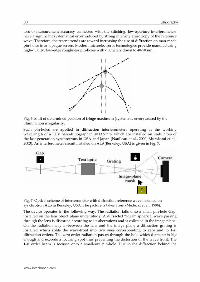
Lithography
80
loss of measurement accuracy connected with the stitching low-aperture interferometers have a significant systematical error induced by strong intensity anisotropy of the reference wave Therefore the recent trends are toward increasing the use of diffraction on man-made pin-holes in an opaque screen Modern microelectronic technologies provide manufacturing high-quality low-edge roughness pin-holes with diameters down to 40-50 nm
Fig 6 Shift of determined position of fringe maximum (systematic error) caused by the illumination irregularity
Such pin-holes are applied in diffraction interferometers operating at the working wavelength of a EUV nano-lithographer λ=135 nm which are installed on undulators of the last generation synchrotrons in USA and Japan (Naulleau et al 2000 Murakami et al 2003) An interferometer circuit installed on ALS (Berkeley USA) is given in Fig 7
Fig 7 Optical scheme of interferometer with diffraction reference wave installed on synchrotron ALS in Berkeley USA The picture is taken from (Medecki et al 1996)
The device operates in the following way The radiation falls onto a small pin-hole Gap installed on the lens object plane under study A diffracted ldquoidealrdquo spherical wave passing through the lens is distorted according to its aberrations and is collected in the image plane On the radiation way in-between the lens and the image plane a diffraction grating is installed which splits the wave-front into two ones corresponding to zero and to 1-st diffraction orders The zero-order radiation passes through the hole which diameter is big enough and exceeds a focusing spot thus preventing the distortion of the wave front The 1-st order beam is focused onto a small-size pin-hole Due to the diffraction behind the
wwwintechopencom
Manufacturing and Investigating Objective Lens for Ultrahigh Resolution Lithography Facilities
81
screen ldquoan idealrdquo spherical wave is generated The reference wave expands toward a CCD-camera where it interferes with a wave passed through the lens under test The measurement accuracy provided by the interferometer will be discussed later when comparing with our interferometer As we can see such interferometers are efficiently used for the final characterization of wave-front aberrations of objectives for EUV radiation At manufacturing stages of substrates and mirrors the producers of the optics usually use optical diffraction interferometers The experimental study of capabilities of point diffraction interferometers operating with a visible light has demonstrated a number of factors reducing the measurement accuracy Particularly systematic discrepancy of experimental data when studying the same optics with the help of visible and EUV light interferometers is observed (Goldberg et al 2002) All of this stimulated to study the way how finite conductance and thickness of the screen material have an effect on amplitude-phase characteristics of the diffracted wave behind the screen and correspondingly on the interferometer measurement accuracy In work (Chkhalo et al 2008) the calculations of the amplitude-phase characteristics of the diffracted field behind the screen in the far-field zone have been carried out They used the solution of a task about the field of a point source located above a half-space with arbitrary properties and covered with a film of any thickness and arbitrary optical constants given in (Dorofeyev et al 2003) Fig 8 illustrates the statement of the problem The diffraction of a flat wave on a circular hole with the radius of a in a film with thickness of hf and the inductivity of f in medias with parameters and 1 was considered The field was calculated behind the screen at Zgt0 on a spherical surface with a fixed radius R0=10 cm The radius R0 was chosen from practical reasons but its value does not produce any effect on the community of the result since the calculation was done for a case krgtgt1 where k=2λ is a wave vector of the diffracted wave in a point with the radius-vector r
Fig 8 Sketch of the geometry of the problem where hf is the thickness of the film heff is an effective film thickness (characterized by the skin-layer) d is the diameter of a hole 1 and f are the dielectric constants of the film and the medias θ1 and θ2 are the angles of diffraction Incident wave is schematically shown by the arrows
The results of the calculations as compared with the solution of classical task of diffraction on zero-thickness superconducting screen have shown that most real electrodynamical
wwwintechopencom
Lithography
82
characteristics of the screen material have an effect on phase characteristics of the diffracted field The calculation of the phase distortions was carried out for the films of aluminum molybdenum tungsten and a number of other materials The results of numerical calculations shown in Fig 9 represent a relative phase deviation on meridional angle of the diffracted scalar field in the case of aluminum different thickness films characterized by dielectric constant Alasymp-542-i218 at the wavelength 633 nm as compared with the case of a perfect screen |Al|rarrinfin The phase incursion ∆(θ) is expressed in nanometers The radius of the hole in the films was а=150 nm A case of free standing (=1=1) films was considered It is evident that the larger the meridional angle the larger is the phase deviation of the diffracted field in the case of a realistic screen We connect the result with an additional phase accumulation due to the field propagation through the real film at larger meridional angles (see Fig 8 for a qualitative clarification) We did not find a thickness dependence on the phase accumulation in the range of lthflt1000 nm where is a skin-layer because the phase can be effectively accumulated only inside the skin-layer The transitions hfrarr0 and |Al|rarrinfin |Al|rarrinfin or hfrarr0 led to the known textbook examples The corresponding diffraction fields for such idealized problems perfectly coincide with those of a spherical phase front
Fig 9 A relative phase deviation ∆(θ)=((0)-(θ))λ2 on meridional angle of the diffracted field in a case of Al different thickness film (Alasymp-542-i218) at the wavelength 633 nm on a spherical surface R0=10 cm the hole radius is а=150 せす
Other mechanisms of the phase distortion can be associated with the excitation of waveguide and surface modes in a plane layer and with a diffraction of such modes by a hole followed by their radiative decay Since the dielectric constant of all materials in soft X-ray and EUV ranges are close to unity Re()asymp1 corresponding phase distortions are minimal It is one of the reasons why the quality of the diffracted reference wave in EUV region has a better result in a higher measurement precision The carried out calculations have shown (see Fig 10) that the angular dependencies of the phase distortions on the meridional angle weakly change for different materials The only exception is osmium for which the phase deformation was extremely low Optical constants of materials used in these calculations were taken from (Palik 1985)
wwwintechopencom
Manufacturing and Investigating Objective Lens for Ultrahigh Resolution Lithography Facilities
83
Fig 10 Angular dependencies of the phase distortions on the meridional angle for different materials
By this means a fundamental limitation of the point diffraction interferometer measurement accuracy is caused by the aberrations of the reference spherical wave induced by the interaction and propagation of secondary waves through the screen material These aberrations are liable to reach a few nanometers depending on the angular aperture If we take into account the polarization characteristics of the light the aberration of the reference wave increases a few times depending on azimuth angle (Dorofeev 2009) The quality of a diffracted wave strongly depends on wave aberrations of preliminary optics focusing the laser beam and the accuracy of adjusting the laser beam axis in respect to the pin-hole center (Otaki et al 2002) All these limit the working aperture of the interferometer and result in the necessity of testing high-aperture optics zones The following stitching procedure of the zonal data raises additional errors All of these disadvantages hinder to widespread use of the point diffraction interferometers in an industry Taking into account all of these problems and limitations the problem of searching for alternative and more perfect methods for the spherical wave generation becomes very urgent
5 Spherical wave source on the basis of tipped fiber
The sources of the spherical wave based on tipped down to a sub-wave exit aperture of the single mode fibers are free from the many of mentioned above problems The application of such fibers as a reference spherical wave source for the point diffraction interferometers has been proposed in (Klimov et al 2008) In Ref (Chkhalo et al 2008) the aberrations of the wave generated by the sources at the wavelength of He-Ne laser =633 nm have been studied These investigations have demonstrated a number of advantages of spherical wave sources as compared with the conventional ones based on a pin-hole in an opaque screen One of the advantages is connected with the fact that in the optical fiber the eigenmodes are excited and correspondingly the quality of the diffracted wave does not depend on aberrations and the mechanical adjustment of the preliminary optics A high degree of homogeneity of the diffracted wave (dgt1) is combined with a high intensity because the light is input into the fiber using high-efficiency methods through a 5-
wwwintechopencom
Lithography
84
microm-diameter core The convex shape of the source Fig 11 decreases the ldquotiprdquo effect bound to the interaction of the off-axis rays with a metallized part of the fiber along the perimeter of the exit aperture The lack of a flat screen around the source significantly decreases diffracted wave distortions connected with the light polarization The well developed methods for handling optical fibers make it possible to easily control the polarization parameters of the diffracted radiation and implement various schemes for interference measurements For instance two or even more coherent sources can be organized with the given polarization of each other
Fig 11 Photographs of the fiber based source taken with scanning electron microscope (marked as a) and b)) and the source with on optical connector
The quality of the diffracted wave of the tipped fiber based source was studied with an interferometer (Kluenkov et al 2008) at two wavelengths =633 nm (He-Ne laser) and =530 nm (second harmonic of Nd-YAG laser) As opposed to the former experiments when in the measurement scheme an optical observation system collected the interfering fronts onto the CCD-camera in present work the data obtained by the direct detection of the fronts on the window-free CCD-camera are given As the experiments showed both the observation systems and even a thin glass window introduce a significant at the level of parts of nanometer error into the measurements
Fig 12 Experimental setup for studying the wave front deformations of the tipped fiber based sources of spherical wave 1 is a laser 2 is a system for input the light into the fiber 3 is a single mode fiber optics coupler 4 is a polarization controller 5 are sources under study 6 is a CCD-camera and 7 is a computer
wwwintechopencom
Manufacturing and Investigating Objective Lens for Ultrahigh Resolution Lithography Facilities
85
The new experimental setup is given in Fig 12 Polarization controllers (item 4 in Fig 12) allow to transform an elliptical polarization of the light at the output of the sources into a linear one as well as to superpose the polarization planes which provide the best contrast of the interference pattern The distance between the sources determining the fringe number (a wedge between two interfering wave fronts) was varied in the range of 1-10 m The measurements were carried out for different angles between the source axes The numerical aperture was varied by approaching (moving off) the CCD camera in respect to the sources A typical interferogram and a wave aberration map obtained in the experiments are shown in Fig 13 The operating wavelength was =530 nm
Fig 13 A typical interferogramm and a wave aberration map observed in the experiments obtained at a wavelength =530 nm
The measured dependencies of the wave deformation RMS on numerical aperture NA of this couple of sources are given in Fig 14 The pictures correspond to the measurements in small (left) and in large (right) numerical apertures Left graphs on both pictures correspond to the experimental data The data obtained with the interferometer installed on the synchrotron ALS in Berkeley USA are marked by stars The interferometer using a pin-hole in an opaque screen as a reference spherical wave source operates at the wavelength =135 nm and is considered as a reference for the measurement accuracy among the point diffraction interferometers (Naulleau et al 1999) It is clearly seen from the pictures that wave front aberrations of the source developed in this work are even less as compared with the ALS-sources despite a longer operating wavelength When analyzing the obtained experimental data there is a need to pay attention to two facts bull Relatively ldquohighrdquo of order λ1000 total aberration of the diffracted waves is observed
at large numerical apertures (NAasymp03) bull Regular structure (symmetry) of the wave front deformation map is clearly seen Such maps and statistical values of the deformations are practically found for all couples of so called ldquohigh qualityrdquo sources The wedge direction between interfering fronts (a line passing through the sources) represents itself as the axis of the symmetry Particularly the deformation map can be put ldquohorizontallyrdquo by turning the wedge through 90 degrees All of this points to the presence of an aberration caused by some kind of physical reason rather than by technological fluctuations This aberration rises with the increase of the observation angle just as it is shown in Figs 9 and 10 In case of understanding the physical nature of this aberration it can be taken into account when reconstructing the true wave deformation (surface shape) that results in increasing the working aperture of the interferometer by a few times
wwwintechopencom
Lithography
86
Fig 14 Averaged over 9 measurements total wave front deformations of couple of the fiber based spherical wave sources depending on numerical aperture (left graphs in both pictures) and ALS-data (Naulleau et al 1999) (stars) Working wavelength is =530 nm First picture corresponds to lower and right ndash to the higher numerical apertures The right graphs in the pictures are corrected according to the geometry of the experiment
This fact of the uniform angular dependence of the aberration let us interpret in a new manner the measurement data obtained in ALS and in our experiments In the Youngrsquos experiment carried out in ALS the least distorted parts of the diffracted waves round their own axes interfere Correspondingly RMS of the aberration is calculated over the range of the cone limited by the numerical aperture NA Opposite to that in our case side parts of the wave fronts interfere Fig 12 in the range from zero degree up to a double value of the angular aperture of the wave front In other words in the search for the wave front aberration RMS the averaging is performed over a double numerical aperture 2NA Therefore the measured dependences presented in Fig 14 (left graphs) can be corrected in the manner as it is shown by arrows (right graphs) As it is seen from the picture the source of the reference spherical wave based on a tipped single mode fiber has a substantially lower wave front aberration and a higher working aperture as compared with the conventional one based on pin-hole in an opaque screen
6 Diffraction interferometer based on a single mode fiber with the sub-wave exit aperture
On the basis of a tipped fiber source of the reference spherical wave the laboratory sample of an interferometer has been developed and manufactured which optical scheme and photo are presented in Figs 15 and 16 The interferometer is installed in a basement thermostated room on a bearer separated from the house footing For the additional protection against vibrations the instrument is installed on 12 bellows under 16 bar pressure Since the measurement accuracy is extremely high the turbulent air flowing inside the interferometer and effecting optical paths along the rays can introduce additional errors To solve these problems the interferometer is placed into a vacuum chamber which is pumped out down to a pressure of 1 Pa
wwwintechopencom
Manufacturing and Investigating Objective Lens for Ultrahigh Resolution Lithography Facilities
87
Fig 15 Optical scheme of the interferometer 1 ndash PC 2 ndash registering system 3 ndash observing system 4 ndash source of spherical wave 5 ndash flat sharp-edge mirror 6 ndash three-axes-controlled precision bench 7 ndash tested concave surface 8 ndash single mode optical fiber 9 ndash polarization controller 10 ndash laser
Fig 16 Photograph of the vertical vacuum interferometer
wwwintechopencom
Lithography
88
The optical scheme shown in Fig 15 corresponds to the interferometer for studying concave spherical or weakly aspherical surfaces The spherical wave source (item 4 Fig 15) is mounted on a high-precision three-axis-controlled bench (item 6 Fig 15) in the direct in a distance of several micrometers proximity from the flat mirror (item 5 Fig 15) The reference spherical wave which after reflecting from the studied surface (item 7 Fig 15) carries the information about its form is focused on a flat mirror and being reflected from it goes into the CCD registering system where it interferes with a part of the reference front directly propagating to the detector The main disadvantage of this scheme is connected with the fact that the investigated sample is irradiated by the most distorted side part of the wave front that practically halves the interferometer operating numerical aperture For solution of this problem in (Kluenkov et al 2008) the scheme of the interferometer with two low-coherent sources of the reference spherical waves has been proposed (Fig 17) In this scheme one source forms the spherical wave laquoSpherical wave 1raquo irradiating the investigated surface while the spherical wave of the second source laquoSpherical wave 2raquo is directed into the registering system The radiation reflected from the investigated surface contains the information on its shape and after reflecting from the flat mirror is directed to the registering system where interferes with the reference laquoSpherical wave 2raquo The main advantage of the scheme is that the axes of the wave fronts coincide with the axes of the investigated surface and the registering system which provides the minimal deformations of reference fronts
Fig 17 Scheme of the low-coherence diffraction interferometer with two sources of the reference spherical wave
As a source of the radiation a super-luminescent diode with a coherence length about 20 microns is applied It prevents parasitic interferences of wave fronts produced by different elements of the optical scheme For observing the correct interference the optical path of the light of source 2 is increased by a double distance from the investigated surface to the sources In this case the interference is observed only for the noted above wave fronts The radiation of the source 1 directly going into the registering system creates only a background signal on the detector
wwwintechopencom
Manufacturing and Investigating Objective Lens for Ultrahigh Resolution Lithography Facilities
89
As it was already marked in diffraction interferometers a divergent spherical wave is used as a reference wave It imposes a number of restrictions on the interferometer capabilities Strictly speaking with their help it is possible to investigate only concave spherical and slightly aspherical surfaces and objectives The measurement of the form of strongly aspherical concave or even spherical but convex surfaces demands using additional optical elements transforming the reference divergent spherical wave to a new one which front is close to the surface shape under study Of special interest are interferometric measurements of objective wave front deformations for example for final certification of the objective wave aberrations or for objective adjustment directly in an interferometer or in the case of the objective application for studying convex spherical surfaces In Fig 18 the scheme and photograph of measurements of six-lens objective in the interferometer are shown In this scheme two coherent sources are used The measured data of the wave deformation were PV = 423 nm and RMS = 82 nm
Fig 18 Scheme of the interferometer with two coherent sources of the reference spherical wave (left) and photograph in the interferometer (right) for testing sixs-lens objective 1 ndash PC 2 ndash registering system 3 ndash observing system 4 ndash source of spherical wave 5 ndash flat sharp-edge mirror 6 ndash three-axes-controlled precision bench 8 ndash single mode optical fiber 9 ndash polarization controller 10 ndash laser 11 ndash studied objective
The certified objective was used for the interferometric measurement (Fig 19) of a convex spherical surface of a special compensator which in turn later on was applied for studying the concave ashpherical surface for a double-mirror objective For reconstructing the true shape of the convex surface the expansion coefficients at basis polynomials corresponding to the objective aberrations were deducted from the measured ones Aspherical surfaces are used in the majority of high-resolution optical objectives in order to widen the field of view of the optical systems Direct testing of aspherical surfaces by using an interferometer with the spherical reference wave is often difficult or even impossible For example Fig 20 a) shows the interferogram for a concave aspherical substrate with about 7-microm deviation of the surface from the nearest sphere The measurements were carried out by using the basic scheme shown in Fig 15 It is evident that a large number of fringes makes
wwwintechopencom
Lithography
90
the position determination of the minima almost impossible Moreover the upper part of the interferogram is simply not there which is explained by a large about 100 microm diameter of the focusing spot for which the beam partially propagates above the edge of mirror (item 5 Fig 15) and misses the measurement system
Fig 19 Optical scheme (left) and photograph of units (right) in the interferometer for certification of convex surfaces Designations on the scheme are the same as in Fig 15
Fig 20 Interferograms from the aspherical concave mirror М2 obtained without wave-front corrector (a) and using corrector (b)
One of the most effective solution of this problem is the use of wave-front correctors ie special optical elements that transform a reference spherical wave front into an aspherical one which shape is identical to the shape of the studied surface In order to take into account the wave-front distortions due to errors of the corrector itself its surfaces should be only spherical In this case it is possible to test these surfaces with subnanometer accuracy by using a spherical reference wave interferometer by the techniques stated above The scheme for testing the concave aspherical surface by using a corrector is presented in Fig 21 The parameters of the corrector suitable for testing the concave aspherical surface
wwwintechopencom
Manufacturing and Investigating Objective Lens for Ultrahigh Resolution Lithography Facilities
91
ie radii of the surfaces thickness and the distance from the reference wave source to the top of the first surface were calculated by minimizing the difference of longitudinal aberrations of the tested aspherical surface and the corrector described in (Malacara 1992 Puryaev 1976) in detail The calculated root-mean-square deviation of the wave front after the corrector from the investigated aspherical shape was RMS=λ1810 This suffices for testing the mirror surface of a nanolithographer with a double-mirror objective It is clearly seen from Fig 20 b) that the interferogram from the aspherical surface obtained by using such a corrector can be reliably processed
Fig 21 Optical scheme (left) and photograph of units in interferometer (right) for certification of concave aspherical surfaces using corrector 1 - computer 2 - registering system 3 - observation system 4 - spherical wave source 5 - flat mirror 6 - 3D precision table 7 - investigated concave aspherical surface 8 - optical fiber 9 - polarization controller 10 - laser 11 - corrector
The analysis of the influence of misalignment in the measurement optical scheme and a thickness error of the compensator on ldquoasphericityrdquo of the wave-front passing through the corrector and accordingly on the measurement accuracy has shown that the requirements for these characteristics of the optical scheme are easily performed in practice In particular the error of a compensator thickness within the limits of plusmn01 mm leads to a wave front aberration at the level of λ1000 Studying of the convex aspherical surfaces is complicated by the fact that besides the corresponding transformation of a spherical front into an aspherical one the corrector must provide a converging front of the wave All of these essentially complicate both the calculation and the design of the corrector In particular in some cases it is necessary to use aspherical surfaces or more than one lens In the case of optics for Schwarzschild objectives this problem is solved easily enough As a corrector the mating concave aspherical mirror which surface has been preliminary tested by using the corrector system described above and corrected according to the procedure described in the next section can be used The measurement scheme is presented in Fig 22 This scheme can be applied for the final
wwwintechopencom
Lithography
92
adjustment and certifications of the objective It is noteworthy to mention that this method can be applied for a convex spherical surface characterization too besides using additional objectives as it is shown in Fig 19
Fig 22 Measurement scheme of aspherical convex mirror М1 using mirror M2 as a wave-front corrector 1 - computer 2 ndash CCD camera 4 - spherical wave source 9-polarization controller 10 ndash laser 11 ndash Schwarzschild objective М1 and М2 ndash convex and concave aspherical mirrors
The measurement accuracy provided by the interferometer depends on many factors including the quality of the reference-wave source the accuracy of determining the positions and a number of interference minima and the accuracy of mathematical retrieval of the surface (wave-front) shape using a limited number of experimental points and the number and degree of the polynomials In turn the accuracy of determining the minimum positions is strongly dependent on the width of the interference pattern the degree of pollution of the interference pattern by ldquoparasiticrdquo interference the method of its rejection the uniformity and intensity of the interfering fronts and a number of other unmanageable factors In this work the interferometer measurement precision was evaluated by studying the rotations of the measured surface maps corresponding to the physical turn of the tested detail The idea of this method is the following If the interferometer provides zero-error measurements then when the detail is rotated the measured surface map should turn correspondingly and the measured statistical parameters of the surface shape deformations should remain unchanged The measured surface deformation maps of a spherical substrate with a numerical aperture NA=014 corresponding to different rotations of the detail are
wwwintechopencom
Manufacturing and Investigating Objective Lens for Ultrahigh Resolution Lithography Facilities
93
presented in Fig 23 The figures demonstrate that the turn of the maps is well observed and the statistical parameters of the deformations change within the limits of RMS=307plusmn0055 nm This test confirms the high measurement accuracy provided by the interferometer which is sufficient for many lithographic applications
Fig 23 Maps and statistical parameters of the surface form deformation corresponding to rotations of the spherical mirror by 0 90 180 and 270 degrees
To summarize this section it is possible to ascertain that the developed interferometer with the diffraction reference wave provides a precision certification of the high-aperture optical surfaces and systems to the subnanometer accuracy
7 Shape correction of optical surfaces to subnanometer accuracy
The developed precise techniques for measuring the shape of optical surfaces made it possible to pass to the main stage the correction of the surface shape made with traditional accuracy λ2 - λ20 depending on the type of optics up to λ1000 - λ2000 In the context of the given work two methods of correction have been developed a vacuum deposition of thin film coatings and ion etching of previously deposited films through metal masks An extremely high accuracy of correcting the surface shape imposes specific requirements on the correction method 1 As a result of the correction process the microroughness of the corrected surface (as a
rule it is initially supersmooth) should remain at the initial level
wwwintechopencom
Lithography
94
2 In the case of a shape correction by means of a local thin film deposition the correcting layers should not distort the substrate surface shape due to intrinsic stress ie they should have a minimally possible stress
3 The correction method should provide the deposition or the removal of materials in a wide range of thickness (1-300 nm) with the accuracy not worse than several percents This problem is especially urgent in the last correction stages when the thickness of the layers to be deposited (removed) is about one nanometer
4 The film materials should allow their complete removal from the substrate (for example chemically) without changing the initial surface shape and microroughness It allows repeating the correction process in the case when the previous correction attempt failed
Researches on stress compensation in multilayer structures and on a substrate restoration have shown that a material meeting all these requirements is CrSc multilayer structure (Salashchenko 2001) The deposition of coatings was made by the magnetron sputtering method The scheme of the correction process and the photograph of the installation are shown in Fig 24 Vacuum in the chamber was (07-1)middot10-6 Tor pressure of working gas (argon) was (07-09)middot10-4 Tor The characteristic power on DC magnetrons was 300-400 W The film thickness control of the deposited layers is performed by variating the passage speed of the corrected surface above the magnetrons sources The stabilization of the discharge power and the argon pressure were provided at the level of 01 The predetermined distribution of the layer thickness over the substrate surface was reached due to the application of figured diaphragms mounted between the magnetron sources and the substrate In addition the substrate rotates around its axis Local values of the film thicknesses over the substrates were measured with an x-ray reflectometer at 447 nm wavelength The details of these measurements will be shown below
Fig 24 Photograph of a technological facility and scheme of surface shape correction by means of multilayer film deposition through masks
The operational experience with this technology has shown a number of important advantages Firstly the roughness of the film surface practically does not depend on the angle of incidence of the atoms in respect to the substrate that allows to carry out the
wwwintechopencom
Manufacturing and Investigating Objective Lens for Ultrahigh Resolution Lithography Facilities
95
correction procedure at normal angles It reduces shadows on the surface increasing the localness of the correction correspondingly Secondly the high accuracy of the layer thickness control up to 1 provides a high reproducibility of the process The film-correction method proved to be efficient for initial stages in which the layers with of tens-hundreds nanometers are deposited in a single correction The process becomes unstable as the thickness of deposited layers decreases down to the units of nanometers Correcting films have changed the proper color that is connected with films oxidation at initial stages of deposition The distribution of oxygen in depth of scandium film obtained with the help of a secondary ion mass-spectroscopy (Drozdov et al 2009) is given in Fig 25 The figure shows an increased content of oxygen on the film surface and at the film-substrate interface Other serious disadvantages of the thin-film-correction method has a discrete and iterative character of the process After each iteration it is necessary to vent the vacuum chamber to make a new diaphragm to pump the chamber again All this strongly decreases the throughput of the process
Fig 25 The distribution of oxygen in depth of scandium film deposited onto Si-substrate
Therefore the application of ion-beam etching at the final correction stage looks very attractive This method allows in particular when focused ion-beams are used to realize the ldquomasklessrdquo correction without frequent opening of the installation to atmosphere Now this method is widely used for substrate form correcting and even for final ion-beam polishing in optical industry (Allen et al 1991 Chason amp Mayer 1993 Ghigo et al 2007) Recently an intensive literature has evolved which is devoted to the application of this method for the precision correction of substrates for projection EUV lithography (Dinger et al 2000 Murakami 2007) For the ion beams applied for the surface shape correction of substrates for EUV and soft X-ray optical elements a number of requirements are imposed the basic of which is the preservation of the surface roughness at an initial (supersmooth) level even when the removed layer depth reaches a few hundreds of nanometers Therefore an optimization of ion energy and incidence angles of the ions on the corrected surface at different depths of material removal is an actual problem Other problems inviting a further investigation are connected with some features of the ion-beam etching at an extremely small depth (asymp 1 nm) removal of materials The experiments have been performed on the installation (Fig 26) with the Cauphmanraquo type ion-beam source KLAN-103M (Website Platar Company 2009) The basic advantage of
wwwintechopencom
Lithography
96
this source is the possibility of working with small ion energies Еi = 50- 300 eV at a significant current density
Fig 26 Photographs of installation for substrates surface shape correction by ion-beam etching
The main characteristics of the ion source are the operating gas is argon or other inert gases the maximal diameter of the ion beam is 100 mm the maximal ion current is 100 mA the maximal ion current density is up to 23 mAcm2 the range of ion energy regulation is 50-1500 eV at the energy spread of plusmn3 eV the discharge working voltage is 35-50 V the thermo-cathode is made of thoriated tungsten (03 mm in diameter) filament Presence of charge-neutralizer (additional thermo-cathode) allows compensating the ion beam charge that provides using the ion source for correction substrates of dielectric materials too The measured dependence of the etching rate of CrSc coating on the removal depth taken at ion energy Еi=200 eV and grazing incidence angle of θ = 42ordm is shown in Fig 27 by dots It is evident that at the initial stage of the etching the removal is less than 120 nm practically a linear increase of the etching rate from the removal depth is observed At a very small etching depth h lt10 nm a wide scatter of the etching rate values is observed Considering the data of the secondary ion mass-spectrometry Fig 28 such a behavior of the etching rate can be explained by oxidation of the sample surface The etching rate of the oxide layer is significantly lower as compared with pure CrSc material If take this into account the calculated etching rate a solid line in Fig 27 matches well the experimental data The observed instability of the etching rate at h lt10 nm might be explained by the variation of the oxidized layer depth in various samples When samples were etched by a neutralized beam (stars in Fig 27) no changes of the rate were observed With the increased ion energy up to 300 eV Fig 29 such instability of the etching rate is not observed either According to atomic-force microscopy measurements the surface roughness remained constant at the level of 02 nm down to 400 nm removal depths For the ion energy of Еi=300 eV when the etching depth exceeds 80 nm an increase of surface roughness is observed (Fig 30)
wwwintechopencom
Manufacturing and Investigating Objective Lens for Ultrahigh Resolution Lithography Facilities
97
Fig 27 Dependence of etching rate on removal depth of CrSc multilayer structures dots are experiment with ions stars are experiment with neutrals and line is calculation accounting etching of the oxidized layer Ion energy Еi = 200 eV and current Ii=60 mA
0 5 10 15 20 25 30 35 40 4500
40x104
80x104
12x105
16x105
Oxigen
SIM
S in
ten
sit
y a
u
Depth nm
Fig 28 Typical distribution of oxygen atoms on depth of CrSc multilayer structure taken by secondary ion mass-spectrometry
The dependences of etching depth on an ion dose (the dose is the product of ion current and etching time) both from the ion current at fixed time and from the time at fixed current show a good linearity that is useful from the practical point of view because it allows to easily define the necessary etching time at a given ion current The example of the dependences of the etching depth on the dose is given in Fig 31 The dashed line corresponds to the linear approximation of the dependence and line with squares represents the experimental data It should be noted that the experiments carried out with greater ion energies up to Ei=15 keV have shown a fast growth of the surface roughness even at small nearby 20ordm grazing angles of incidence of the ions on the surfaces (Chkhalo et al 2008)
wwwintechopencom
Lithography
98
Fig 29 Dependence of ion etching rate on etching depth of CrSc multilayer structures at ion energy Еi = 300 eV (area of small removal depths)
Fig 30 Dependence of surface roughness of CrSc multilayer structures on etching depth at sputtering by argon ions with energy Еi = 300 eV
Fig 31 Dependence of etching depth of the CrSc multilayer structures on ions doze at ion energy Еi = 300 eV - - - linear approximation of the dependence
0 20 40 60 80 1000
10
20
30
40
Etc
hin
g d
ep
th n
m
Dosage mAmin
wwwintechopencom
Manufacturing and Investigating Objective Lens for Ultrahigh Resolution Lithography Facilities
99
For correcting the surface shape of substrates for imaging X-ray optics when the subnanometer form accuracy is required the following strategy providing minimal time expenses has been chosen At the initial stage when peak-to-valley values (P-V) of the surface shape are 50-200 nm the local deposition of the thin films is applied Then at the reduction of the P-V values down to 10-20 nm the ion beams with the energy of 200 eV are used At the final correction stage the 300 eV-ions are applied Figure 32 illustrates the result of using this correction procedure for a spherical substrate with a numerical aperture of NA=025 (the diameter is 130 mm and the curvature radius is 260 mm) which was initially the standard etalon for a conventional interferometer The initial surface map is shown in Fig 32 a) The parameters of the surface were P-V=426 nm and RMS=73 nm The surface shape improved to P-V=73 nm and RMS=06 nm (Fig 32 b)) Thus a root-mean-square deviation of the initial surface shape from an ideal sphere has decreased in 12 times ie in units of the interferometer working wavelength (=0633 microm) it has became better than λ1000 The photograph of this mirror mounted on a metal frame is given in Fig 33
Fig 32 Maps of deviations of the spherical surface shape from the nearest ideal sphere a) initial shape (P-V=426 nm RMS=73 nm) b) after 12-th correction (P-V=73 nm RMS=06 nm)
Fig 33 Photograph of the multilayer spherical mirror for 135 nm wavelength in the frame Diameter of the working aperture is 130 mm
wwwintechopencom
Lithography
100
In spite of a greater wavelength of the traditional deep ultraviolet lithography (193 nm) because of a great number of lens and high requirements for the quality of the projective objectives the methods of correction and certification with a subnanometer accuracy described in this article are urgent for the refracting optics too In connection with this the researches on etching of fused quartz surfaces by ion beams with a compensated charge have been carried out As well as in the case of metal surfaces the main attention was given to the etching rate to the reproducibility of the etching process and to the surface microroughness depending on the beam characteristics incidence angles and material removal depths In Fig 34 the dependences of quartz etching depth on the etching dose are presented The dashed lines in the figure correspond to linear approximations of the dependencies The ion energy was 200 and 300 eV the grazing incidence angle was 42ordm The comparison with similar dependences for CrSc Fig 31 shows that the etching rate of fused quartz is almost twice as much No nonlinearity at the initial stage of the etching is observed that on the one hand proves the hypothesis about the effect of the oxide layer in the case of CrSc material and on the other hand essentially facilitates the correction process
0 100 200 300 4000
50
100
150
200
250
300
350
Etc
hin
g d
ep
th n
m
Dosage mAmin
Fig 34 Dependences of the etching depth on the doze for fused quartz Etching is performed by argon ions with compensated charge and with energy Еi = 200 and 300 eV - - - - linear approximation of dependences
The data on the surface roughness of a fused quartz substrate etched by ions (neutrals) with energies of 200 and 300 eV for various removal depths measured by means of the atomic-force microscope and by x-ray diffractometry are presented in table 1 The substrates manufactured by General optics (USA) were used in the experiment The minimal roughness of initial surfaces measured with an atomic-force microscope was 013 nm and with the x-ray reflection it was about 04 nm From the table it is evident that atomic-force microscope measurements have shown a weaker influence of the etching process on the surface roughness in comparison with the roughness measurements made by the x-ray diffractometry method A more detailed discussion of this difference is beyond the given article Thus the presented experimental data show that these technologies of vacuum deposition and ion-beam etching in the aggregate allow to correct with a subnanometer accuracy the surface shape of optical elements practically of any materials (metals dielectrics semiconductors) with keeping the surface on a supersmooth level This technology is
wwwintechopencom
Manufacturing and Investigating Objective Lens for Ultrahigh Resolution Lithography Facilities
101
suitable for manufacturing elements for imaging x-ray optics and for high resolution systems in visible and deep ultra-violet ranges
Table 1 Roughness of fused quartz substrates depending on neutral (ion) energy and etching depths measured by atomic-force microscopy (AFM) and x-ray diffractometry (X-ray) methods
8 Reflecting multilayer interference mirrors
The final stage of manufacturing a precise mirror for ultrahigh resolution imaging x-ray optical systems is the procedure of the deposition of multilayer reflecting coating on a substrate A low polarizability of materials (le1) and correspondingly a small jump of the refraction factor Δn=00001-01 on the vacuum-material interface and a strong absorption of the radiation by all materials completely exclude the application of refractive optics in the extreme ultra-violet and soft x-ray ranges Because of a low reflection from one interface the reflection optics of normal incidence can be only interferential and the number of layers demanded for the achievement of a high reflectivity depending on a wavelength can reach a value of 102-103 The absorption of the radiation in multilayer structures leads to the fact that the reflectivity is always less than unity While choosing an optimal pair of materials providing a maximal reflectivity on a given wavelength the circumstance is often used that in the range of wavelengths directly adjoining the absorption edge of the material gt AE (AE is the wavelength of the material absorption edge) and coinciding with an anomalous dispersion of the optical constants the lowest absorption and the maximal polarizability of materials are observed For some materials in the field of K-and L- absorption edges the refraction factor can even exceed unity In Fig 35 the calculated spectral dependences of the maximal reflection coefficients for the most attractive pairs of materials in a spectral range of 3 - 16 nm representing the biggest interest for projection nanolithography and high resolution x-ray microscopy are shown The greatest experimental reflectivity about 70 was obtained at a wavelength of 135 nm The spectral range around λasymp67 nm (area of boron anomalous dispersion) is of interest for projection x-ray lithography However the reflectivity obtained here with LaB4C multilayer mirrors at a normal angle of incidence does not exceed 45-47 (Andreev et al 2009) that is not enough for lithographic applications
wwwintechopencom
Lithography
102
2 3 4 5 6 7 8 9 10 11 12 13 14 15 1600
01
02
03
04
05
06
07
08
CrSc
CrC
LaB
MoBe
MoSi
experiment
Refle
ctivity
Wavelength nm
Fig 35 Calculated (lines with symbols) and experimental (stars (Website ESRF 2006 Andreev et al 2003)) reflection coefficients of mostly attractive pairs of materials in X-ray and EUV ranges
On the short-wave length side the working wavelength of the normal incidence multilayer optics is limited by technology capabilities for depositing high-quality short period multilayer structures At present the shortest periods have multilayer structures based on WB4C (the period dasymp1 nm) (Vainer et al 2006 Platonov 2002) and CrSc (dasymp15 nm) (Salashchenko amp Shamov 1997 Website ESRF 2006) A number of special requirements are imposed on the multilayers which should be deposited onto substrates for imaging optics In particular to provide a constructive interference of the waves reflected from different interfaces the radiation wavelength λ the local angle of incidence ( )rθ f
and the period of the multilayer structure ( )d rf should satisfy
the Bragg condition
( )2sin ( )
d rr
λθ=f
f (11)
where rf is a radius-vector of a point of incidence of the radiation on the structure As the
incidence angles are a function of the coordinates it results in the necessity to deposit multilayer structures with a variable over the surface period so-called ldquogradedrdquo structures In some cases for example when the angular divergence of the X-ray beam falling on one point of the mirror surface exceeds the Braggrsquos peak width the multilayer structure should have a variable period on depth (Kozhevnikov et al 2001) One more important feature of multilayer structures for precise optics can be explained as follows For multilayer dispersive elements the maximum deviation of the local value of the period d from the nominal one is determined by the condition of synchronism of the waves reflected from various interfaces which can be expressed through the spectral selectivity of a mirror 1 S d d Nδλ λ δ= = cong (N is a number of periods) In the case of precision multilayer imaging optics when the required surface shape accuracy is at a subnanometer
wwwintechopencom
Manufacturing and Investigating Objective Lens for Ultrahigh Resolution Lithography Facilities
103
level to the synchronism condition an extra requirement for the preservation of the mirror surface shape is added For example for the well-known MoSi multilayer structure optimized on the wavelength of λ=135 nm the period is dasymp7 nm at a number of periods N asymp 40 Correspondingly the general thickness of the structure is L=Nd=280 nm The local error of the period of 1 will affect weakly on reflectivity however the surface shape of the mirror will produce a change of 28 nm which already can essentially produce an influence on imaging properties of the mirror From these simple estimations two important conclusions follow Firstly when designing and manufacturing the surface shape of a substrate it is necessary to take into account the real thickness of a multilayer coating which would be deposited onto the substrate Secondly it is necessary to provide a high at a level of 02-03 accuracy of local values of the period over the mirror surface Besides an intrinsic stress in the multilayer structures which can also deform the surface shape must be taken into account The estimation of the deformation x of a substrate with a diameter D a thickness hsub with the Yung modulus E and the Poisson factor ν on which a hf thick film with the intrinsic stress σ is deposited can be performed by means of equations
2
2
3
4
1
f
sub
h Dx
Y h
EY
σδ
ν
sdot sdot= sdotsdot= minus
(12)
For instance for optimized on maximum of the reflection coefficient MoSi multilayer structure (portion of Mo layer in the period =dMo(dMo+dSi) = 04) the stress in our case is about σ =-350 М『а (Fig 36) At deposition of such a multilayer structure (general thickness is L=Nd=280 nm) on a substrate of fused quartz with the diameter D=220 mm and thickness h=50 mm (Y=844 》а) the maximal deformation of the substrate surface would be about 17 nm that essentially exceeds an admissible level of the surface shape deformation of a mirror for EUV lithography Different groups solve this problem in different ways One the solution is the use of mirrors with a specified thickness ratio of molybdenum layer in the periods Mo asymp 05 - 07 when the stress is close to zero (Windt et al 1994 Zoethout et al 2003) The other solution consists in adding a third material into the periods for example Ru (Oshino et al 2003) However all these methods either because of a stronger absorption of EUV radiation or because of an interface roughness growth have smaller of 10-20 absolute values of the reflectivity In IPM RAS a technique of the stress compensation based on the use of special sublayers lying under the basic MoSi multilayer structure is under development For CrSc multilayer structures the stress is close to zero at γCr=dCr(dCr+dSc)asymp05 (Fig 37 (Andreev et al 2005)) At γCrgt05 a sign of the stress is positive on the contrary to the MoSi structures at γMo= 04 when it is negative The total stress σeff in the structure consisting of CrSc and MoSi multilayer films can be determined from a ratio
( ) ( )
( ) ( )Mo Si Mo Si Mo Si Cr Sc Cr Sc Cr Sc
eff
Mo Si Mo Si Cr Sc Cr Sc
d N d N
d N d N
σ σσ ⎡ ⎤sdot sdot + sdot sdot⎣ ⎦= sdot + sdot (13)
from which it follows that optimizing the composition and the thickness of CrSc layers it is possible to compensate the stress in the basic MoSi reflecting multilayer structure
wwwintechopencom
Lithography
104
Fig 36 Stress in MoSi multilayer structures depending on ratio of Mo layer in period γMo=dMo(dMo+dSi) at fixed period d=697 nm
Fig 37 Stress in CrSc multilayer structure depending on ratio of Cr layer in period γCr=dCr(dCr+dSc) at fixed period d=54 nm
In practice it is necessary to consider a process of the stress relaxation which depending on the structure and materials is variable over several days Totally the stress can change by tens percent An example of such a process is illustrated in Fig 38 in which the time dependencies of the stress in multilayer structures consisting of anti-stress CrSc sublayers and MoSi reflecting layers are presented The structures differ by thicknesses of the sublayers It is necessary to note that the stress value is affected not only by ratio of the layer thickness in the period but also by the period size and conditions in which the films were deposited For depositing multilayer structures a method of magnetron spattering is used in IPM RAS The method allows depositing films onto curved as well as flat substrates The conditions under which multilayer structures are deposited are briefly described in section 6 devoted to the correction of the substrate surface shape by the method of local thin-film deposition The facilities have from two to six magnetron sources that allows depositing at one technological cycle reflecting anti-stress and anti-diffusion barrier layers Now the
σ MP
a
-1000
-800
-600
-400
-200
0
200
400
600
02 04 06 08 10
γMo=dMo (dMo+dSi)
0
100
200
300
400
500
600
700
06 065 07 075
σ MP
a
γCr = dCr (dCr+dSc)
wwwintechopencom
Manufacturing and Investigating Objective Lens for Ultrahigh Resolution Lithography Facilities
105
technologies of depositing more than twenty various pairs of materials are developed It allows manufacturing optics for a whole x-ray and extreme ultra-violet spectral range More details about the properties of the multilayer structures can be found in (Andreev et al 2003)
Fig 38 Stress in MoSi multilayer structures with anti-stress CrSc sublayers versus of time a) - [(CrSc)times42 d=538 nm =067 (MoSi))times45 d=698 nm =04] and b) - [(CrSc)times40 d=538 nm =067 (MoSi)times45 d=698 nm =04]
A great volume of works high requirements for the coating quality and for accuracy of the period distribution over a substrate surface dictate the need for an operative information about characteristics of the deposited coatings with the purpose of correcting the technological process It is most convenient to perform such work with the presence of laboratory reflectometers allowing the investigation of multilayer structures on working wavelengths and located in the immediate vicinity of technologists Therefore laboratory reflectometers are constantly being developed and improved recently In Refs (Loyen et al 2003 Miyake et al 2003 Gulikson et al 1992) the specialized reflectometers for investigating multilayer optics in the range around 135 nm are described As a source of the soft x-ray and EUV radiation the laser plasma is used which arises due to the irradiation of solid-state targets by laser light with a power density about 109 Wcm2 For monochromatization the radiation spherical diffraction gratings operating at grazing angles are used The characteristic fluxes of the photons in the working range of wavelengths of 10-16 nm on the investigated samples with the probe beam size asymp 2 mm are 107 - 108 photons (01 nmtimess) The results of reflectivity measurements of MoSi multilayer mirrors in the area of 135 nm obtained with the help of these reflectometers as compared with the data obtained with a PTB-reflectometer (synchrotron BESSY-2 Berlin Germany which is considered as the reference one) have shown the coincidence of the measured reflection coefficients at a level of 3 and the resonant wavelength asymp 001 nm The basic disadvantages of these reflectometers in our opinion are a narrow range of working wavelengths and a low spectral resolution caused by the applied monochromator scheme The monochromator consists of two stationary slits and spherical (or toroidal) diffraction grating Scanning across the spectrum is carried out due to the diffraction gratings rotation around its axis According to this arrangement the position of the slits and the diffraction grating coincides with the Rowland circle (Rowland 1893) only for one
-30
-20
-10
0
10
20
30
50 100 15 200 250
Time hours
σ eff
MP
a
a)
t days
σ MPa
- 40
- 30
- 20
- 10
0
1 2 3 4 5 6 7 8 9
x
x
xx
x x
b)
wwwintechopencom
Lithography
106
wavelength that essentially limits the range where the spectral resolution of the monochromator is kept at the acceptable level of Δλapp asymp 001-002 nm The other factor limiting working spectral range of the reflectometer is the type of the used radiation source (laser plasma) which large size does not allow scanning by the entrance slit of the grating spectrometer Our group develops multilayer optics for a wide spectral range λ=06-50 nm and the monochromator spectral resolution up to 0003-0005 nm is frequently required Therefore in IPM RAS laboratory reflectometers on the basis of high resolution grating monochromators have been developed These monochromators have a movable entrance slit and diffraction grating (Chkhalo et al 1998 Zuev amp Mitrofanov 2002 Bibishkin et al 2004 Bibishkin et al 2005) In the reflectometrs the monochromators of type RSM-500 (Lukirsky et al 1967) and McPherson-247 (Website Mcpherson Company 2009) are used The photograph and optical scheme of the last generation reflectometer are given in Fig 39 Owing to such a spectrometer the kinematic scheme slits and diffraction grating are always located in the Rowland focusing circle so that the high spectral resolution of the device in the whole range of wavelengths is provided Two diffraction gratings with various radiuses of curvature cover this spectral range
Fig 39 Optical scheme and photograph of the reflectometer XRT - x-ray tube S1 S2 - entrance and exit slits AS VS - horizontal and vertical anti-scattering slits DG - diffraction grating TM - toroidal mirror M ndash probe beam intensity monitor MIS - investigated sample D ndash detector G5 ndash five-axes goniometer
In the reflectometer the radiation from the anode of the x-ray tube (XRT) through the entrance slit of the monochromator (S1) falls on the diffraction grating (DG) The diffracted monochromatic radiation according to the diffraction grating equation cosϕ - cosψ =mλD (m - the order of diffraction λ ndash a wavelength and D - the grating period ϕ and ψ angles of diffraction and incidence correspondingly) is focused onto the spectrometer exit slit S2 Scanning across the spectrum is carried out by linear moving of the diffraction grating and the exit slit with a simultaneous turn of the diffraction grating so that the condition Xl=Rgsdot sinψ where Rg - radius and Xl - distance between the diffraction grating center and the exit slit is satisfied An anti-scattering diaphragm (AS) reduces the intensity of scattered radiation at the output of the monochromator and limits the irradiated area of the diffraction grazing The monochromatic radiation by means of a toroidal mirror (TM) is focused on the investigated sample The other important function of the toroidal mirror is connected with a filtration of higher diffraction orders which is especially urgent when
wwwintechopencom
Manufacturing and Investigating Objective Lens for Ultrahigh Resolution Lithography Facilities
107
working with bremsstrahlung of the tungsten anode Radiuses of the toroidal mirror are chosen in such a way that in a horizontal plane the exit slit and in a vertical plane the source are imaged on the sample under study The studied sample is installed on a five-axis goniometer which photograph and scheme of movements are shown in Fig 40 The linear translation along X and Z axes the rotation around them (ω and ) and the inclination θ allow to insert any point of the sample under study with a diameter up to 300 mm into the x-ray beam The detector executes 2 rotation The additional inclination of the detector 2θ allows to increase the numerical aperture of the sample which can be tested up to NA=05
Fig 40 Photograph of the goniometer and scheme of movements provided by the goniometer
The concept of a spectrometer-monochromator with a movable slit and diffraction grating became possible only due to the application of the dismountable x-ray tube of an original design as the radiation source The advantages of classical sealed x-ray tubes are their small dimensions and weight simplicity in operation sufficient for reflectometric applications intensity of the x-ray radiation and long life-time However the application of these sources for precision reflectometry in soft x-ray and extreme ultra-violet ranges has shown that because of the fast contamination of the anode by products of thermocathode material erosion and hydrocarbons decomposition under a powerful electron-beam emission characteristics and life-time of the tubes collapsed when comparing with expected values For solving this problem in our work the tube was equipped with an ion-beam source for cleaning anodes from contaminations (Bibishkin et al 2003) It allows to work without opening the spectrometer and the tube to the atmosphere within several months thus approaching its operation mode to the traditional sealed X-ray tubes for hard X-rays The work is done on K L and M characteristic lines of target (anode) materials and on continuous bremsstrahlung spectrum of tungsten On one holder about 8 targets of various materials are installed It is necessary to note that frequently it is possible to use a few spectral lines from one target
wwwintechopencom
Lithography
108
As an illustration in Fig 41 the measured spectral dependence of reflectivity of MoSi multilayer spherical mirror shown in Fig 40 is presented The measurement has been performed with the reflectometer at an incidence angle of the radiation to the sample of 5ordm (from the local normal)
Fig 41 Spectral dependence of the reflection coefficient of MoSi multilayer mirror deposited onto spherical substrate Angle of incidence was 5ordm from the local normal
One more important advantage of the x-ray tube as a source of X-ray radiation is that in the field of wavelengths lt3 nm because of aberrations of spherical grating the spectral width of the probe beam is ΔGge 001 nm while the spectral resolution of short period multilayers reaches values Δ MIS lt001 nm Since the natural width of characteristic lines of some materials in this range is essentially less than this value this circumstance provides precision measurements of reflective characteristics of multilayer mirrors even when monochromator does not provide the demanded resolution Thus the developed in IPM RAS methods of multilayer coating deposition stress compensation in the film structures laboratory metrology of the mirrors at working wavelengths restoration of the substrates without any damage of the substrate surface shape and roughness allow us to make and certify high reflecting multilayer mirrors with a sub-nanometer level surface shape accuracy attended for super-high resolution imaging X-ray optics
9 Conclusion
In the given article the basic researches and the full cycle of developed in IPM RAS technologies and metrology techniques from the substrate surface shape correction to the deposition of multilayer coatings on them which are required for manufacturing high reflecting mirrors for diffraction quality imaging in the extreme ultra-violet and in the soft X-ray ranges are described As a whole it is evident that the problem of manufacturing such optics for high resolution EUV lithography and X-ray microscopy is already solved as a first approximation The further activity should be directed toward the increase of both in manufacturing accuracy of optical surfaces up to a level of RMS=01 nm and in the numerical aperture of objectives up to NA=04-06
0
10
20
30
40
50
60
70
126 130 134 138 142
Wavelength nm
Refl
ect
ivit
y
wwwintechopencom
Manufacturing and Investigating Objective Lens for Ultrahigh Resolution Lithography Facilities
109
In this connection upgrading the interferometric methods for surface shape measurements of optical elements and wave-front deformations of objectives first of all and regarding the increase of their working numerical aperture is a subject of current interest The diffraction interferometers utilizing the tipped fiber as a source of the reference spherical wave look rather attractive Owing to the simplicity of the design high intensity of the diffracted wave weak sensitivity to the adjustment in an optical circuit and a number of other advantages the interferometers which are simple in operation can be developed for the optical industry In the framework of the given article the problem arising when aspherical surfaces are under investigation of development and optimization of correctors transforming the reference spherical fronts into the aspherical ones which shapes are identical to the shapes of the studied surfaces was not practically discussed Meanwhile traditional lens null-correctors have limited capabilities rather complicated in manufacturing and expensive and demand complicated calibrating procedures for taking into account the wave-front distortions due to errors of the corrector itself In this connection diffraction correctors represent a significant interest (Akatov et al 2004) A gross potential for the surface shape correction of dielectric materials by means of ion-beams has RF-etching in chemically active environments The first experiments on etching of quartz substrates by means of the RF-etching have shown that the surface micro-roughness did not change down to the removal depths of a few micrometers (Akhsakhalyan et al 2008) The most serious problem on the way of manufacturing the effective optics for the soft X-ray radiation λlt10 nm is that reflection coefficients of the multiplayer mirrors are not sufficiently high Nevertheless the results that have been recently obtained in the field of the X-ray optics teams may be considered as a break-through because they lay the foundation of developing such important physico-technological directions as projection EUV nanolithography X-ray microscopy and extraterrestrial astronomy of the ultrahigh resolution
10 References
Akhsakhalyan AD Vainer YuA Volgunov DG Drozdov MN Kluenkov EB Kuznetcov MI Salashchenko NN Kharitonov AI amp Chkhalo NI (2008) Application of reactive ion-beam etching for surface shape correction of X-ray mirrors Proceedings of Workshop ldquoX-ray optics ndash 2008rdquo pp 26-28 Chernogolovka Moscow region 6-9 October 2008 p 26-28 IPTM Chernogolovka (in Russian)
Allen LN Keim RE amp Lewis TS (1991) Surface error correction of a Keck 10 m telescope primary mirror segment by ion figuring Proceedings SPIE Vol 1531 1991 pp 195ndash204
Andreev SS Bulgakova SA Gaponov SV Gusev SA Zuev SYu Kluenkov EB Luchin VI Lopatin AYa Mazanova LM Prokhorov KA Sadova EN Salashchenko NN amp Shamov EA (2000) Investigations in field of projection lithography of extreme ultraviolet region in Institute for physics of microstructures RAS Surface X-ray synchrotron and neutron investigations Vol 1 2000 pp 32-41 (in Russian)
Andreev SS Akhsakhalyan AD Bibishkin MS Chkhalo NI Gaponov SV Gusev SA Kluenkov EB Prokhorov KA Salashchenko NN Schafers F amp Zuev
wwwintechopencom
Lithography
110
SYu (2003) Multilayer optics for XUV spectral region technology fabrication and applications Central European Journal of Physics Vol 1 2003 pp 191-209
Adreev SS Kluenkov EB Misinov AL Polkovnikov VN Salashchenko NN Suslov LA amp Chernov VV (2005) Compensation of elastic deformation of MoSi multilayer structures on quartz and zerodur substrates using buffer CrSc technique Surface investigations Vol 2 2005 pp 45-48 (In Russian)
Andreev SS Barysheva MM Chkhalo NI Gusev SA Pestov AE Polkovnikov VN Salashchenko NN Shmaenok L A Vainer YuA amp Zuev SYu (2009) Multilayered mirrors based on LaB4C(B9C) for x-ray range near anomalous dispersion of boron ( near 67 nm) Nuclear Instruments and Methods in Physics Research SecA Vol 603 2009 pp 80-82
Archer KM (1997) Craniofacial reconstruction using hierarchical b-spline interpolationrdquo A thesis submitted in partial fulfilment of the reguirements for the degree of master of applied science The university of British Columbia 1997 p 113
Asadchikov VE Kapabekov AYu Kozhevnikov IV Levashov VE amp Sagitov SI (1998) Experimental investigation of roughness correlation of a film and a substrate by means of X-ray scattering Crystallography Vol 43 No 1 1998 pp 119-130 (In Russian)
Barbee TW (Jr) (1981) Sputtered layered synthetic microstructures (LSM) dispersion elements Proceedings of Conference ldquoLow energy X-ray diagnosticsrdquo pp 131-145 Monterey USA 1981 N Y Amer Inst Phys
Benschop JPH Kaiser WM amp Ockwell DC (1999) EUCLIDES the European EUVL program SPIE Symposium on Micro-lithography Vol 3676 1999 p 246
Bibishkina MS Zabrodin IG Klyuenkov EB Salashchenko NN Chekhonadskih DP amp Chkhalo NI (2003) A new dismountable tube for soft X-ray radiation Surface investigations No 2 2003 pp 41-45 (In Russian)
Bibishkinb MS Zuev SYu Salashchenko NN amp Chkhalo NI (2003) Measuring of microroughness of surfaces using soft X-ray radiation Surface investigations No 1 2003 pp 94-96 (In Russian)
Bibishkin MS Chekhonadskih DP Chkhalo NI Klyuenkov EB Pestov AE Salashchenko NN Shmaenok LA Zabrodin IG amp Zuev SYu (2004) Laboratory methods for investigation of multilayer mirrors in Extreme Ultraviolet and Soft X-Ray region Proceedings of SPIE Vol 5401 2004 pp 8-15
Bibishkin MS Vainer YuA Pestov AE Prokhorov KA Salashchenko NN Fraerman AA amp Chkhalo NI (2005) Investigation of characteristics of multilayer X-ray mirrors with ultra-short periods d = 07-24 せす Bulletin of the Russian Academy of Sciences Physics Vol 69 No 2 2005 pp 199-206
Blunt R (2006) White light interferometry - a production worthy technique for measuring surface roughness on semiconductor wafers Proceedings of CEMANTECH Conference pp 59-62 Vancouver Canada April 24-27 2006
Born M amp Wolf E (1973) Principles of optics second edition Science Moscow (In Russian)
Braat J (1987) Polynomial expansion of severely aberrated wave fronts Optical Society of America Vol 4 No 4 1987 pp 643-650
Chason E amp Mayer T M (1993) Low energy ion bombardment induced roughening and smoothing of Si02 surfaces Applied Physics Letters Vol 62 No 4 1993 pp 363-365
Cheng P (1987) Instrumentation and Biological Applications In X-ray Microscopy Springer Verlag
wwwintechopencom
Manufacturing and Investigating Objective Lens for Ultrahigh Resolution Lithography Facilities
111
Chkhalo NI Dolbnya IG Fedorchenko MV Kruglyakov EP Zarodyshev AV amp Zolotarev KV (1993) Multilayer mirror on copper-nickel substrates for intense X-ray beams Proceedings of the 4-th International Conference ldquoX-Ray Microscopy 4rdquo pp 586-592 Russia Chernogolovka September 20-24 1993 IPTM Chernogolovka
Chkhalo NI Fedorchenko MV Kruglyakov EP Volokhov AI Baraboshkin KS Komarov VF Kostyakov SI amp Petrov EA (1995) Ultradispersed diamond powders of detonation nature for polishing X-ray mirrors Nuclear Instruments and Methods in Physics Research A Vol 359 1995 pp 155-156
Chkhalo NI Kirpotin AN Kruglyakov EP amp Semenov EP (1998) Reflectometer for precision tests of optical components in the ultrasoft X-ray range Nuclear Instruments and Methods in Physics Research A Vol 405 1998 pp 393-395
Chkhaloa NI Raskin DG amp Salashchenko NN (2008) Capabilities of microinterferometer with digital recording of images for studying micro-objects with sub-nanometer resolution Proceedings of SPIE Vol 7025 2008 p 702512
Chkhalob NI Dorofeyev IA Salashchenko NN amp Toropov MN (2008) A plane wave diffraction on a pin-hole in a film with a finite thickness and real electrodynamic properties Proceedings of SPIE Vol 7025 2008 p 702506
Chkhaloc NI Klimov AYu Rogov VV Salashchenko NN amp Toropov MN (2008) A source of a reference spherical wave based on a single mode optical fiber with a narrowed exit aperture Rev Sci Instrum Vol 79 2008 p 033107
Chkhalod N Paramonov L Pestov A Raskin D amp Salashchenko N (2008) Correction of the EUV mirror substrate shape by ion beam Proceedings of SPIE Vol 7025 2008 p 702503
Dinger U Bisert F Lasser H Mayer M Seifert A Seitz G Stacklies S Stickel F-J amp Weise M (2000) Mirror substrates for EUV-lithography progress in metrology and optical fabrication technology Proceedings of SPIE Vol 4146 2000 pp 35ndash46
Dorofeyev I Jersch J amp Fuchs H (2003) Spectral composition of electromagnetic fluctuations induced by a lossy layered system Annalen der Physik Vol 12 No 7-8 2003 pp 421-437
Dorofeev I (2009) Amplitude-phase characteristics of electromagnetic fields diffracted by a hole in a thin film with realistic optical properties Physica E Vol 41 2009 pp 762-770
Drozdov MN Drozdov YuN Barysheva MM Polkovnikov VN amp Chkhalo NI (2009) Minimization of matrix effects upon layer-by-layer analysis of multilayer metallic nanostructures LaB4C by SIMS using cluster secondary ions Proceedings of Symposium ldquoNanophysics and nanoelectronicsrdquo Vol 1 pp 190-191 Nizhniy Novgorod Russia 16-20 March 2009 IPM RAS Nizhniy Novgorod (in Russian)
Gavrilin DA (2003) Investigations of methods for shape description of complicated optical surfaces at interferometrical control PhD thesis St-Petersburg Russia 103 p (in Russian)
Ghigo M Canestrari R Spiga D amp Novi A (2007) Correction of high spatial frequency errors on optical surfaces by means of Ion Beam Figuring Proceedings of SPIE Vol 6671 2007 p 667114
Goldberg KA amp Kevin G (2001) Wave-front measurement errors from restricted concentric subdomains J Opt Soc Am A Vol 18 No 9 2001 pp
wwwintechopencom
Lithography
112
Goldberg KA Naulleau P Bokor J Chapman HN amp Barty A (2002) Testing extreme ultraviolet optics with visible-light and extreme ultraviolet interferometry J Vac Sci Technol B Vol 20 No 6 2002 pp 2834-2839
Griffith J E amp Grigg DA (1993) Dimensional metrology with scanning probe microscopes Journal of Applied Physics Vol 74 1993 pp R83-R109
Gullikson EM Underwood JH Batson PC and Nikitin V (1992) A soft X-rayEUV reflectometer based on a laser produced plasma source Journal of x-ray science and technology Vol 3 1992 pp 283-299
Gwyn C (1998) White paper on Extreme ultraviolet Lithography Proceedings of EUV LLC 1998 Livermore
Klimov AYu Rogov VV Salashchenko NN amp Chkhalo NI (2008) A Spherical Wave Source Based on a Probe for a Near-Field Microscope Bulletin of the Russian Academy of Sciences Physics Vol 72 No 2 2008 pp 204-206
Kluyenkova EB Pestov AE Polkovnikov VN Raskin DG Toropov MN Salashchenko NN amp Chkhalo NI (2008) Testing and Correction of Optical Elements with Subnanometer Precision Nanotechnologies in Russia Vol 3 Nos 9-10 2008 pp 602-610
Klyuenkovb EB Polkovnikov VN Salashchenko NN amp Chkhalo NI (2008) Shape Correction of Optical Surfaces with Subnanometer Precision Problems Status and Prospects Bulletin of the Russian Academy of Sciences Physics Vol 72 No 2 2008 pp 188-191
Kozhevnikov IV Asadchikov VE Duparre A Gilev ON Havronin NA Krivonosov YuS Ostashev VI amp Steinert J (1999) Comparative study of the roughness of optical surfaces and thin films using atomic force microscopy x-ray scattering and light scattering methods Proceedings of SPIE Vol 3739 1999 pp 348-354
Kozhevnikov IV Bukreeva IN amp Ziegler E (2001) Nuclear Instruments and Methods in Physics Research Sec A Vol 460 2001 p 424
Linnik VP (1933) A simple interferometer to test optical systems Bulletin of the Academy of Science of the USSR Vol 1 1933 pp 210-212
Loyen L Bottger T Braun S Mai H Leson A Scholze F Tummler J Ulm G Legall H Nickels PV Sandner W Stiel H Rempel C Schulze M Brutscher J Macco F amp Mullender S (2003) A New Laboratory EUV Reflectometer for Large Optics using a Laser Plasma Source Proceedings of SPIE Vol 5038 2003 pp 12-21
Lukirsky AP Brytov IA amp Komyak NI (1967) Prototype of an X-ray spectrometer with diffraction grating and ionization detection for spectral region of 10-55 Aring Apparatus and methods of X-ray analysis No 2 1967 pp 4-19 L Engineering (in Russian)
Malacara D ed (1992) Optical shop testing 2nd ed John Wiley amp Sons Inc ISBN 0-471-52232-5 New York
Medecki H Tejnil E Goldberg KA amp Bokor J (1996) Phase-shifting point diffraction interferometer Optics letters Vol 21 No 19 1996 pp 1526-1528
Miyake A Miyachi T Amemiya M Hasegawa T Ogushi N Yamamoto T Masaki F amp Watanabe Y (2003) LPP-based reflectometer for characterization of EUV lithography systems Proceedings of SPIE Vol 5037 2003 pp 647-655
Murakami K Saito Y Ota K et al (2003) Development of an experimental EUV interferometer for benchmarking several EUV wavefront metrology schemes Proceedings of SPIE Vol 5037 2003 pp 75-82
wwwintechopencom
Manufacturing and Investigating Objective Lens for Ultrahigh Resolution Lithography Facilities
113
Murakami K Oshino T Kondo H Chiba H Komatsuda H Nomura K amp Iwata H (2007) Development of optics for EUV lithography tools Proceedings of SPIE Vol 6517 2007 pp 65170J
Naulleau PP Goldberg KA Lee SH Chang C Attwood D amp Bokor J (1999) Extreme-ultraviolet phase-shifting point-diffraction interferometer a wave-front metrology tool with subangstrom reference-wave accuracy Appl Opt Vol 38 No 35 1999 pp 7252-7263
Naulleau P Goldberg KA Lee SH Chang Ch Atwood D amp Bokor J (2000) The EUV phase-shifting point diffraction interferometer Synchrotron Radiation Instrumentation Eleventh US National Conference ed by P Pianetta p 66-72 ISBN 1-56396-941-6 American Institute of Physics
Naulleau P Golberg KA Anderson EH et al (2002) Sub-70 nm Extreme Ultraviolet Lithography at the Advanced Light Source Static Microfield Exposure Station Using the Engineering Test Stand Set-2 Optic Jour Vac Sci Technol B Vol 20 2002 pp 2829ndash2833
Nevot L amp Croce P (1980) Characterisation des surfaces par reflection rasante de rayon Application a lrsquoetude du polissage de quelque verres silicates Revue de Physique Appliquee Vol 15 1980 pp 761-779
Okatov MA Antonov EA Baigozhin A et al (2004) Handbook for optical-technologist St- Petersburg Politechnica 2004 679 p
Oshino T Shiraishi M Kandaka N Sugisaki K Kondo H Ota K Mashima K Murakami K Oizumi H Nishiyama I amp Okazaki S (2003) Development of illumination optics and projection optics for high-NA EUV exposure tool (HiNA) Proceedings of SPIE Vol 5037 2003 pp 75-82
Ota K Murakami K Kondo H Oshino T Sugisaki K amp Komatsuda H (2001) Feasibility study of EUV scanners Proceedings of SPIE Vol 4343 2001 pp 60-69
Otaki K Ota K Nishiyama I Yamamoto T Fukuda Y amp Okazaki S (2002) Development of the point diffraction interferometer for extreme ultraviolet lithography Design fabrication and evaluation J Vac Sci Technol B Vol 20 No 6 2002 pp 2449-2458
Palik ED (1985) Hanbook of optical constants of solids Naval Research Laboratory Washington DC 1985 749 pp
Parratt LG (1954) Surface studies of solids by total reflection of x-rays Physical Review Vol 35 1954 pp 359-369
Platonov Yu Gomez L amp Broadway D (2002) Proceedings of SPIE Vol 4782 2002 p 152 Protopopov VV Valiyev KA amp Imamov RM (1999) Measurement of spatial
distribution of superpolished surface roughness and defects in multilayer X-ray mirrors Surface investigations No 1 1999 pp 111-119 (In Russian)
Puryaev DT (1976) Methods for control of aspherical surfaces M Engineering 1976 13 p (in Russian)
Rodionov SA Przhevalinsky LI amp Shekhonin AA (1974) Application of coefficients of interpolation polynomial for optical system aberrations presentation Bulletin of the USSR institutions of higher education Instrument engineering Vol 17 No 10 1974 p 104 (in Russian)
Rodionov SA (1995) Mthematical apparatus for ptics control ndash general approach Optical journal No 8 1995 pp 49-51
Rowland H (1893) Gratings in theory and practice Phil Mag Vol 35 1893 p 397 Salashchenko NN amp Shamov EA (1997) Optics communication Vol 134 1997 p 7
wwwintechopencom
Lithography
114
Salashchenko NN (2001) Optical Element and Method for Recovering the Substrate Patent DE 101 01 820 A1 00074P
Sinha SK Sirota EB Garoff S amp Stanley HB (1988) X-ray and neutron scattering from rough surfaces Physical Rev B Vol 38 No4 1988 pp 2297-2311
Sommargren GE (1996) Diffraction methods raise interferometer accuracy Laser Focus World Vol 8 1996 p 61-71
Soufli R Spiller E Schmidt MA Davidson JC Grabner RF Gullikson EM Kaufmann BB Mrowka S Baker SL Chapman HN Hudyma RM Taylor JS Walton ChC Montcalm C amp Folta JA (2001) Multilayer optics for an extreme ultraviolet lithography tool with 70 nm resolution Proceedings of SPIE Vol 4343 2001 pp 51-59
Stone VW Jonas AM Nysten B amp Legras R (1999) Roughness of free surfaces of bulk amorphous polymers as studied by x-ray surface scattering and atomic force microscopy Physical Rev B Vol 60 No 8 1999 pp 5883-5894
Sun X Chen S amp Shen Q (1998) Geometric calibration of lens using B-spline surface fitting Wuhan University Journal of Natural Sciences Vol 3 No 4 1998 pp 440-442
Swantner W amp Weng W C (1994) Gram-Schmidt orthogonalisation of Zernike polynomials for general aperture shapes Applied optics Vol 33 No 10 1994 pp 1832-1837
Sweeney DW Hudyma RM Chapman HN amp Shafer D (1998) EUV optical design for a 100 nm CD imaging system Proceedings of SPIE Vol 3331 1998 pp 2-10
Underwood JH amp Barbee (Jr) TW (1981) Layered synthetic microstructures as Bragg diffractors for X-rays and extreme ultraviolet theory and predicted performance Appl Opt Vol 20 1981 pp 3027-3034
Vainer YuA Pestov AE Prokhorov KA Salashchenko NN Fraerman AA Chernov VV amp Chkhalo NI (2006) Analysis of Cross-Correlation of Interface Roughness in Multilayer Structures with Ultrashort Periods Journal of Experimental and Theoretical Physics Vol 103 No 3 2006 pp 346-353
Warburton WK Rek ZU amp Barbee (Jr) TW (1987) Quality Investigation of multilayer covers for X-ray optics In X-ray optics and microscopy pp 222-231 World Moscow (In Russian)
Website ESRF httpwwwesrfeueventsconferencespast-conferences-and-workshops pxrms06Detailed-programm12_gulliksonpdf
Website GO Corporation httpwwwgoochandhousegocomproductscat3 Website Mcpherson Company httpwwwmcphersoninccomspectrometers
xuhvvuvuvxuhvvuvuvhtm Website Platar Company httpwwworcru~platarP1Rhtml Website Veeco Instruments httpwwwveecocom Website Zygo Corporation httpwwwzygocom Williamson DM (1995) The elusive diffraction limit OSA Proceedings on Extreme
Ultraviolet Lithography F Zernike and DT Attwood eds Vol 23 1995 pp 68-76 Windt DL Brown WL Volkert CA amp Waskiewicz WK (1994) J Appl Phys Vol 78
1994 p 2423 Zoethout E Sipos G van de Kruijs RWE Yakshin AE Louis E Mullender S amp
Bijkerk F (2003) Stress mitigation in MoSi multilayers for EUV lithography Proceedings of SPIE Vol 5037 2003 pp 872ndash878
Zuev SYu amp Mitrofanov AV (2002) Measurements of parameters of optical elements for X-ray telescopes Surface investigations No 1 2002 pp 81-83 (In Russian)
wwwintechopencom
LithographyEdited by Michael Wang
ISBN 978-953-307-064-3Hard cover 656 pagesPublisher InTechPublished online 01 February 2010Published in print edition February 2010
InTech EuropeUniversity Campus STeP Ri Slavka Krautzeka 83A 51000 Rijeka Croatia Phone +385 (51) 770 447 Fax +385 (51) 686 166wwwintechopencom
InTech ChinaUnit 405 Office Block Hotel Equatorial Shanghai No65 Yan An Road (West) Shanghai 200040 China
Phone +86-21-62489820 Fax +86-21-62489821
Lithography the fundamental fabrication process of semiconductor devices plays a critical role in micro- andnano-fabrications and the revolution in high density integrated circuits This book is the result of inspirationsand contributions from many researchers worldwide Although the inclusion of the book chapters may not be acomplete representation of all lithographic arts it does represent a good collection of contributions in this fieldWe hope readers will enjoy reading the book as much as we have enjoyed bringing it together We would liketo thank all contributors and authors of this book
How to referenceIn order to correctly reference this scholarly work feel free to copy and paste the following
NI Chkhalo AE Pestov NN Salashchenko and MN Toropov (2010) Manufacturing and InvestigatingObjective Lens for Ultrahigh Resolution Lithography Facilities Lithography Michael Wang (Ed) ISBN 978-953-307-064-3 InTech Available from httpwwwintechopencombookslithographymanufacturing-and-investigating-objective-lens-for-ultrahigh-resolution-lithography-facilities
copy 2010 The Author(s) Licensee IntechOpen This chapter is distributedunder the terms of the Creative Commons Attribution-NonCommercial-ShareAlike-30 License which permits use distribution and reproduction fornon-commercial purposes provided the original is properly cited andderivative works building on this content are distributed under the samelicense

Manufacturing and Investigating Objective Lens for Ultrahigh Resolution Lithography Facilities
81
screen ldquoan idealrdquo spherical wave is generated The reference wave expands toward a CCD-camera where it interferes with a wave passed through the lens under test The measurement accuracy provided by the interferometer will be discussed later when comparing with our interferometer As we can see such interferometers are efficiently used for the final characterization of wave-front aberrations of objectives for EUV radiation At manufacturing stages of substrates and mirrors the producers of the optics usually use optical diffraction interferometers The experimental study of capabilities of point diffraction interferometers operating with a visible light has demonstrated a number of factors reducing the measurement accuracy Particularly systematic discrepancy of experimental data when studying the same optics with the help of visible and EUV light interferometers is observed (Goldberg et al 2002) All of this stimulated to study the way how finite conductance and thickness of the screen material have an effect on amplitude-phase characteristics of the diffracted wave behind the screen and correspondingly on the interferometer measurement accuracy In work (Chkhalo et al 2008) the calculations of the amplitude-phase characteristics of the diffracted field behind the screen in the far-field zone have been carried out They used the solution of a task about the field of a point source located above a half-space with arbitrary properties and covered with a film of any thickness and arbitrary optical constants given in (Dorofeyev et al 2003) Fig 8 illustrates the statement of the problem The diffraction of a flat wave on a circular hole with the radius of a in a film with thickness of hf and the inductivity of f in medias with parameters and 1 was considered The field was calculated behind the screen at Zgt0 on a spherical surface with a fixed radius R0=10 cm The radius R0 was chosen from practical reasons but its value does not produce any effect on the community of the result since the calculation was done for a case krgtgt1 where k=2λ is a wave vector of the diffracted wave in a point with the radius-vector r
Fig 8 Sketch of the geometry of the problem where hf is the thickness of the film heff is an effective film thickness (characterized by the skin-layer) d is the diameter of a hole 1 and f are the dielectric constants of the film and the medias θ1 and θ2 are the angles of diffraction Incident wave is schematically shown by the arrows
The results of the calculations as compared with the solution of classical task of diffraction on zero-thickness superconducting screen have shown that most real electrodynamical
wwwintechopencom
Lithography
82
characteristics of the screen material have an effect on phase characteristics of the diffracted field The calculation of the phase distortions was carried out for the films of aluminum molybdenum tungsten and a number of other materials The results of numerical calculations shown in Fig 9 represent a relative phase deviation on meridional angle of the diffracted scalar field in the case of aluminum different thickness films characterized by dielectric constant Alasymp-542-i218 at the wavelength 633 nm as compared with the case of a perfect screen |Al|rarrinfin The phase incursion ∆(θ) is expressed in nanometers The radius of the hole in the films was а=150 nm A case of free standing (=1=1) films was considered It is evident that the larger the meridional angle the larger is the phase deviation of the diffracted field in the case of a realistic screen We connect the result with an additional phase accumulation due to the field propagation through the real film at larger meridional angles (see Fig 8 for a qualitative clarification) We did not find a thickness dependence on the phase accumulation in the range of lthflt1000 nm where is a skin-layer because the phase can be effectively accumulated only inside the skin-layer The transitions hfrarr0 and |Al|rarrinfin |Al|rarrinfin or hfrarr0 led to the known textbook examples The corresponding diffraction fields for such idealized problems perfectly coincide with those of a spherical phase front
Fig 9 A relative phase deviation ∆(θ)=((0)-(θ))λ2 on meridional angle of the diffracted field in a case of Al different thickness film (Alasymp-542-i218) at the wavelength 633 nm on a spherical surface R0=10 cm the hole radius is а=150 せす
Other mechanisms of the phase distortion can be associated with the excitation of waveguide and surface modes in a plane layer and with a diffraction of such modes by a hole followed by their radiative decay Since the dielectric constant of all materials in soft X-ray and EUV ranges are close to unity Re()asymp1 corresponding phase distortions are minimal It is one of the reasons why the quality of the diffracted reference wave in EUV region has a better result in a higher measurement precision The carried out calculations have shown (see Fig 10) that the angular dependencies of the phase distortions on the meridional angle weakly change for different materials The only exception is osmium for which the phase deformation was extremely low Optical constants of materials used in these calculations were taken from (Palik 1985)
wwwintechopencom
Manufacturing and Investigating Objective Lens for Ultrahigh Resolution Lithography Facilities
83
Fig 10 Angular dependencies of the phase distortions on the meridional angle for different materials
By this means a fundamental limitation of the point diffraction interferometer measurement accuracy is caused by the aberrations of the reference spherical wave induced by the interaction and propagation of secondary waves through the screen material These aberrations are liable to reach a few nanometers depending on the angular aperture If we take into account the polarization characteristics of the light the aberration of the reference wave increases a few times depending on azimuth angle (Dorofeev 2009) The quality of a diffracted wave strongly depends on wave aberrations of preliminary optics focusing the laser beam and the accuracy of adjusting the laser beam axis in respect to the pin-hole center (Otaki et al 2002) All these limit the working aperture of the interferometer and result in the necessity of testing high-aperture optics zones The following stitching procedure of the zonal data raises additional errors All of these disadvantages hinder to widespread use of the point diffraction interferometers in an industry Taking into account all of these problems and limitations the problem of searching for alternative and more perfect methods for the spherical wave generation becomes very urgent
5 Spherical wave source on the basis of tipped fiber
The sources of the spherical wave based on tipped down to a sub-wave exit aperture of the single mode fibers are free from the many of mentioned above problems The application of such fibers as a reference spherical wave source for the point diffraction interferometers has been proposed in (Klimov et al 2008) In Ref (Chkhalo et al 2008) the aberrations of the wave generated by the sources at the wavelength of He-Ne laser =633 nm have been studied These investigations have demonstrated a number of advantages of spherical wave sources as compared with the conventional ones based on a pin-hole in an opaque screen One of the advantages is connected with the fact that in the optical fiber the eigenmodes are excited and correspondingly the quality of the diffracted wave does not depend on aberrations and the mechanical adjustment of the preliminary optics A high degree of homogeneity of the diffracted wave (dgt1) is combined with a high intensity because the light is input into the fiber using high-efficiency methods through a 5-
wwwintechopencom
Lithography
84
microm-diameter core The convex shape of the source Fig 11 decreases the ldquotiprdquo effect bound to the interaction of the off-axis rays with a metallized part of the fiber along the perimeter of the exit aperture The lack of a flat screen around the source significantly decreases diffracted wave distortions connected with the light polarization The well developed methods for handling optical fibers make it possible to easily control the polarization parameters of the diffracted radiation and implement various schemes for interference measurements For instance two or even more coherent sources can be organized with the given polarization of each other
Fig 11 Photographs of the fiber based source taken with scanning electron microscope (marked as a) and b)) and the source with on optical connector
The quality of the diffracted wave of the tipped fiber based source was studied with an interferometer (Kluenkov et al 2008) at two wavelengths =633 nm (He-Ne laser) and =530 nm (second harmonic of Nd-YAG laser) As opposed to the former experiments when in the measurement scheme an optical observation system collected the interfering fronts onto the CCD-camera in present work the data obtained by the direct detection of the fronts on the window-free CCD-camera are given As the experiments showed both the observation systems and even a thin glass window introduce a significant at the level of parts of nanometer error into the measurements
Fig 12 Experimental setup for studying the wave front deformations of the tipped fiber based sources of spherical wave 1 is a laser 2 is a system for input the light into the fiber 3 is a single mode fiber optics coupler 4 is a polarization controller 5 are sources under study 6 is a CCD-camera and 7 is a computer
wwwintechopencom
Manufacturing and Investigating Objective Lens for Ultrahigh Resolution Lithography Facilities
85
The new experimental setup is given in Fig 12 Polarization controllers (item 4 in Fig 12) allow to transform an elliptical polarization of the light at the output of the sources into a linear one as well as to superpose the polarization planes which provide the best contrast of the interference pattern The distance between the sources determining the fringe number (a wedge between two interfering wave fronts) was varied in the range of 1-10 m The measurements were carried out for different angles between the source axes The numerical aperture was varied by approaching (moving off) the CCD camera in respect to the sources A typical interferogram and a wave aberration map obtained in the experiments are shown in Fig 13 The operating wavelength was =530 nm
Fig 13 A typical interferogramm and a wave aberration map observed in the experiments obtained at a wavelength =530 nm
The measured dependencies of the wave deformation RMS on numerical aperture NA of this couple of sources are given in Fig 14 The pictures correspond to the measurements in small (left) and in large (right) numerical apertures Left graphs on both pictures correspond to the experimental data The data obtained with the interferometer installed on the synchrotron ALS in Berkeley USA are marked by stars The interferometer using a pin-hole in an opaque screen as a reference spherical wave source operates at the wavelength =135 nm and is considered as a reference for the measurement accuracy among the point diffraction interferometers (Naulleau et al 1999) It is clearly seen from the pictures that wave front aberrations of the source developed in this work are even less as compared with the ALS-sources despite a longer operating wavelength When analyzing the obtained experimental data there is a need to pay attention to two facts bull Relatively ldquohighrdquo of order λ1000 total aberration of the diffracted waves is observed
at large numerical apertures (NAasymp03) bull Regular structure (symmetry) of the wave front deformation map is clearly seen Such maps and statistical values of the deformations are practically found for all couples of so called ldquohigh qualityrdquo sources The wedge direction between interfering fronts (a line passing through the sources) represents itself as the axis of the symmetry Particularly the deformation map can be put ldquohorizontallyrdquo by turning the wedge through 90 degrees All of this points to the presence of an aberration caused by some kind of physical reason rather than by technological fluctuations This aberration rises with the increase of the observation angle just as it is shown in Figs 9 and 10 In case of understanding the physical nature of this aberration it can be taken into account when reconstructing the true wave deformation (surface shape) that results in increasing the working aperture of the interferometer by a few times
wwwintechopencom
Lithography
86
Fig 14 Averaged over 9 measurements total wave front deformations of couple of the fiber based spherical wave sources depending on numerical aperture (left graphs in both pictures) and ALS-data (Naulleau et al 1999) (stars) Working wavelength is =530 nm First picture corresponds to lower and right ndash to the higher numerical apertures The right graphs in the pictures are corrected according to the geometry of the experiment
This fact of the uniform angular dependence of the aberration let us interpret in a new manner the measurement data obtained in ALS and in our experiments In the Youngrsquos experiment carried out in ALS the least distorted parts of the diffracted waves round their own axes interfere Correspondingly RMS of the aberration is calculated over the range of the cone limited by the numerical aperture NA Opposite to that in our case side parts of the wave fronts interfere Fig 12 in the range from zero degree up to a double value of the angular aperture of the wave front In other words in the search for the wave front aberration RMS the averaging is performed over a double numerical aperture 2NA Therefore the measured dependences presented in Fig 14 (left graphs) can be corrected in the manner as it is shown by arrows (right graphs) As it is seen from the picture the source of the reference spherical wave based on a tipped single mode fiber has a substantially lower wave front aberration and a higher working aperture as compared with the conventional one based on pin-hole in an opaque screen
6 Diffraction interferometer based on a single mode fiber with the sub-wave exit aperture
On the basis of a tipped fiber source of the reference spherical wave the laboratory sample of an interferometer has been developed and manufactured which optical scheme and photo are presented in Figs 15 and 16 The interferometer is installed in a basement thermostated room on a bearer separated from the house footing For the additional protection against vibrations the instrument is installed on 12 bellows under 16 bar pressure Since the measurement accuracy is extremely high the turbulent air flowing inside the interferometer and effecting optical paths along the rays can introduce additional errors To solve these problems the interferometer is placed into a vacuum chamber which is pumped out down to a pressure of 1 Pa
wwwintechopencom
Manufacturing and Investigating Objective Lens for Ultrahigh Resolution Lithography Facilities
87
Fig 15 Optical scheme of the interferometer 1 ndash PC 2 ndash registering system 3 ndash observing system 4 ndash source of spherical wave 5 ndash flat sharp-edge mirror 6 ndash three-axes-controlled precision bench 7 ndash tested concave surface 8 ndash single mode optical fiber 9 ndash polarization controller 10 ndash laser
Fig 16 Photograph of the vertical vacuum interferometer
wwwintechopencom
Lithography
88
The optical scheme shown in Fig 15 corresponds to the interferometer for studying concave spherical or weakly aspherical surfaces The spherical wave source (item 4 Fig 15) is mounted on a high-precision three-axis-controlled bench (item 6 Fig 15) in the direct in a distance of several micrometers proximity from the flat mirror (item 5 Fig 15) The reference spherical wave which after reflecting from the studied surface (item 7 Fig 15) carries the information about its form is focused on a flat mirror and being reflected from it goes into the CCD registering system where it interferes with a part of the reference front directly propagating to the detector The main disadvantage of this scheme is connected with the fact that the investigated sample is irradiated by the most distorted side part of the wave front that practically halves the interferometer operating numerical aperture For solution of this problem in (Kluenkov et al 2008) the scheme of the interferometer with two low-coherent sources of the reference spherical waves has been proposed (Fig 17) In this scheme one source forms the spherical wave laquoSpherical wave 1raquo irradiating the investigated surface while the spherical wave of the second source laquoSpherical wave 2raquo is directed into the registering system The radiation reflected from the investigated surface contains the information on its shape and after reflecting from the flat mirror is directed to the registering system where interferes with the reference laquoSpherical wave 2raquo The main advantage of the scheme is that the axes of the wave fronts coincide with the axes of the investigated surface and the registering system which provides the minimal deformations of reference fronts
Fig 17 Scheme of the low-coherence diffraction interferometer with two sources of the reference spherical wave
As a source of the radiation a super-luminescent diode with a coherence length about 20 microns is applied It prevents parasitic interferences of wave fronts produced by different elements of the optical scheme For observing the correct interference the optical path of the light of source 2 is increased by a double distance from the investigated surface to the sources In this case the interference is observed only for the noted above wave fronts The radiation of the source 1 directly going into the registering system creates only a background signal on the detector
wwwintechopencom
Manufacturing and Investigating Objective Lens for Ultrahigh Resolution Lithography Facilities
89
As it was already marked in diffraction interferometers a divergent spherical wave is used as a reference wave It imposes a number of restrictions on the interferometer capabilities Strictly speaking with their help it is possible to investigate only concave spherical and slightly aspherical surfaces and objectives The measurement of the form of strongly aspherical concave or even spherical but convex surfaces demands using additional optical elements transforming the reference divergent spherical wave to a new one which front is close to the surface shape under study Of special interest are interferometric measurements of objective wave front deformations for example for final certification of the objective wave aberrations or for objective adjustment directly in an interferometer or in the case of the objective application for studying convex spherical surfaces In Fig 18 the scheme and photograph of measurements of six-lens objective in the interferometer are shown In this scheme two coherent sources are used The measured data of the wave deformation were PV = 423 nm and RMS = 82 nm
Fig 18 Scheme of the interferometer with two coherent sources of the reference spherical wave (left) and photograph in the interferometer (right) for testing sixs-lens objective 1 ndash PC 2 ndash registering system 3 ndash observing system 4 ndash source of spherical wave 5 ndash flat sharp-edge mirror 6 ndash three-axes-controlled precision bench 8 ndash single mode optical fiber 9 ndash polarization controller 10 ndash laser 11 ndash studied objective
The certified objective was used for the interferometric measurement (Fig 19) of a convex spherical surface of a special compensator which in turn later on was applied for studying the concave ashpherical surface for a double-mirror objective For reconstructing the true shape of the convex surface the expansion coefficients at basis polynomials corresponding to the objective aberrations were deducted from the measured ones Aspherical surfaces are used in the majority of high-resolution optical objectives in order to widen the field of view of the optical systems Direct testing of aspherical surfaces by using an interferometer with the spherical reference wave is often difficult or even impossible For example Fig 20 a) shows the interferogram for a concave aspherical substrate with about 7-microm deviation of the surface from the nearest sphere The measurements were carried out by using the basic scheme shown in Fig 15 It is evident that a large number of fringes makes
wwwintechopencom
Lithography
90
the position determination of the minima almost impossible Moreover the upper part of the interferogram is simply not there which is explained by a large about 100 microm diameter of the focusing spot for which the beam partially propagates above the edge of mirror (item 5 Fig 15) and misses the measurement system
Fig 19 Optical scheme (left) and photograph of units (right) in the interferometer for certification of convex surfaces Designations on the scheme are the same as in Fig 15
Fig 20 Interferograms from the aspherical concave mirror М2 obtained without wave-front corrector (a) and using corrector (b)
One of the most effective solution of this problem is the use of wave-front correctors ie special optical elements that transform a reference spherical wave front into an aspherical one which shape is identical to the shape of the studied surface In order to take into account the wave-front distortions due to errors of the corrector itself its surfaces should be only spherical In this case it is possible to test these surfaces with subnanometer accuracy by using a spherical reference wave interferometer by the techniques stated above The scheme for testing the concave aspherical surface by using a corrector is presented in Fig 21 The parameters of the corrector suitable for testing the concave aspherical surface
wwwintechopencom
Manufacturing and Investigating Objective Lens for Ultrahigh Resolution Lithography Facilities
91
ie radii of the surfaces thickness and the distance from the reference wave source to the top of the first surface were calculated by minimizing the difference of longitudinal aberrations of the tested aspherical surface and the corrector described in (Malacara 1992 Puryaev 1976) in detail The calculated root-mean-square deviation of the wave front after the corrector from the investigated aspherical shape was RMS=λ1810 This suffices for testing the mirror surface of a nanolithographer with a double-mirror objective It is clearly seen from Fig 20 b) that the interferogram from the aspherical surface obtained by using such a corrector can be reliably processed
Fig 21 Optical scheme (left) and photograph of units in interferometer (right) for certification of concave aspherical surfaces using corrector 1 - computer 2 - registering system 3 - observation system 4 - spherical wave source 5 - flat mirror 6 - 3D precision table 7 - investigated concave aspherical surface 8 - optical fiber 9 - polarization controller 10 - laser 11 - corrector
The analysis of the influence of misalignment in the measurement optical scheme and a thickness error of the compensator on ldquoasphericityrdquo of the wave-front passing through the corrector and accordingly on the measurement accuracy has shown that the requirements for these characteristics of the optical scheme are easily performed in practice In particular the error of a compensator thickness within the limits of plusmn01 mm leads to a wave front aberration at the level of λ1000 Studying of the convex aspherical surfaces is complicated by the fact that besides the corresponding transformation of a spherical front into an aspherical one the corrector must provide a converging front of the wave All of these essentially complicate both the calculation and the design of the corrector In particular in some cases it is necessary to use aspherical surfaces or more than one lens In the case of optics for Schwarzschild objectives this problem is solved easily enough As a corrector the mating concave aspherical mirror which surface has been preliminary tested by using the corrector system described above and corrected according to the procedure described in the next section can be used The measurement scheme is presented in Fig 22 This scheme can be applied for the final
wwwintechopencom
Lithography
92
adjustment and certifications of the objective It is noteworthy to mention that this method can be applied for a convex spherical surface characterization too besides using additional objectives as it is shown in Fig 19
Fig 22 Measurement scheme of aspherical convex mirror М1 using mirror M2 as a wave-front corrector 1 - computer 2 ndash CCD camera 4 - spherical wave source 9-polarization controller 10 ndash laser 11 ndash Schwarzschild objective М1 and М2 ndash convex and concave aspherical mirrors
The measurement accuracy provided by the interferometer depends on many factors including the quality of the reference-wave source the accuracy of determining the positions and a number of interference minima and the accuracy of mathematical retrieval of the surface (wave-front) shape using a limited number of experimental points and the number and degree of the polynomials In turn the accuracy of determining the minimum positions is strongly dependent on the width of the interference pattern the degree of pollution of the interference pattern by ldquoparasiticrdquo interference the method of its rejection the uniformity and intensity of the interfering fronts and a number of other unmanageable factors In this work the interferometer measurement precision was evaluated by studying the rotations of the measured surface maps corresponding to the physical turn of the tested detail The idea of this method is the following If the interferometer provides zero-error measurements then when the detail is rotated the measured surface map should turn correspondingly and the measured statistical parameters of the surface shape deformations should remain unchanged The measured surface deformation maps of a spherical substrate with a numerical aperture NA=014 corresponding to different rotations of the detail are
wwwintechopencom
Manufacturing and Investigating Objective Lens for Ultrahigh Resolution Lithography Facilities
93
presented in Fig 23 The figures demonstrate that the turn of the maps is well observed and the statistical parameters of the deformations change within the limits of RMS=307plusmn0055 nm This test confirms the high measurement accuracy provided by the interferometer which is sufficient for many lithographic applications
Fig 23 Maps and statistical parameters of the surface form deformation corresponding to rotations of the spherical mirror by 0 90 180 and 270 degrees
To summarize this section it is possible to ascertain that the developed interferometer with the diffraction reference wave provides a precision certification of the high-aperture optical surfaces and systems to the subnanometer accuracy
7 Shape correction of optical surfaces to subnanometer accuracy
The developed precise techniques for measuring the shape of optical surfaces made it possible to pass to the main stage the correction of the surface shape made with traditional accuracy λ2 - λ20 depending on the type of optics up to λ1000 - λ2000 In the context of the given work two methods of correction have been developed a vacuum deposition of thin film coatings and ion etching of previously deposited films through metal masks An extremely high accuracy of correcting the surface shape imposes specific requirements on the correction method 1 As a result of the correction process the microroughness of the corrected surface (as a
rule it is initially supersmooth) should remain at the initial level
wwwintechopencom
Lithography
94
2 In the case of a shape correction by means of a local thin film deposition the correcting layers should not distort the substrate surface shape due to intrinsic stress ie they should have a minimally possible stress
3 The correction method should provide the deposition or the removal of materials in a wide range of thickness (1-300 nm) with the accuracy not worse than several percents This problem is especially urgent in the last correction stages when the thickness of the layers to be deposited (removed) is about one nanometer
4 The film materials should allow their complete removal from the substrate (for example chemically) without changing the initial surface shape and microroughness It allows repeating the correction process in the case when the previous correction attempt failed
Researches on stress compensation in multilayer structures and on a substrate restoration have shown that a material meeting all these requirements is CrSc multilayer structure (Salashchenko 2001) The deposition of coatings was made by the magnetron sputtering method The scheme of the correction process and the photograph of the installation are shown in Fig 24 Vacuum in the chamber was (07-1)middot10-6 Tor pressure of working gas (argon) was (07-09)middot10-4 Tor The characteristic power on DC magnetrons was 300-400 W The film thickness control of the deposited layers is performed by variating the passage speed of the corrected surface above the magnetrons sources The stabilization of the discharge power and the argon pressure were provided at the level of 01 The predetermined distribution of the layer thickness over the substrate surface was reached due to the application of figured diaphragms mounted between the magnetron sources and the substrate In addition the substrate rotates around its axis Local values of the film thicknesses over the substrates were measured with an x-ray reflectometer at 447 nm wavelength The details of these measurements will be shown below
Fig 24 Photograph of a technological facility and scheme of surface shape correction by means of multilayer film deposition through masks
The operational experience with this technology has shown a number of important advantages Firstly the roughness of the film surface practically does not depend on the angle of incidence of the atoms in respect to the substrate that allows to carry out the
wwwintechopencom
Manufacturing and Investigating Objective Lens for Ultrahigh Resolution Lithography Facilities
95
correction procedure at normal angles It reduces shadows on the surface increasing the localness of the correction correspondingly Secondly the high accuracy of the layer thickness control up to 1 provides a high reproducibility of the process The film-correction method proved to be efficient for initial stages in which the layers with of tens-hundreds nanometers are deposited in a single correction The process becomes unstable as the thickness of deposited layers decreases down to the units of nanometers Correcting films have changed the proper color that is connected with films oxidation at initial stages of deposition The distribution of oxygen in depth of scandium film obtained with the help of a secondary ion mass-spectroscopy (Drozdov et al 2009) is given in Fig 25 The figure shows an increased content of oxygen on the film surface and at the film-substrate interface Other serious disadvantages of the thin-film-correction method has a discrete and iterative character of the process After each iteration it is necessary to vent the vacuum chamber to make a new diaphragm to pump the chamber again All this strongly decreases the throughput of the process
Fig 25 The distribution of oxygen in depth of scandium film deposited onto Si-substrate
Therefore the application of ion-beam etching at the final correction stage looks very attractive This method allows in particular when focused ion-beams are used to realize the ldquomasklessrdquo correction without frequent opening of the installation to atmosphere Now this method is widely used for substrate form correcting and even for final ion-beam polishing in optical industry (Allen et al 1991 Chason amp Mayer 1993 Ghigo et al 2007) Recently an intensive literature has evolved which is devoted to the application of this method for the precision correction of substrates for projection EUV lithography (Dinger et al 2000 Murakami 2007) For the ion beams applied for the surface shape correction of substrates for EUV and soft X-ray optical elements a number of requirements are imposed the basic of which is the preservation of the surface roughness at an initial (supersmooth) level even when the removed layer depth reaches a few hundreds of nanometers Therefore an optimization of ion energy and incidence angles of the ions on the corrected surface at different depths of material removal is an actual problem Other problems inviting a further investigation are connected with some features of the ion-beam etching at an extremely small depth (asymp 1 nm) removal of materials The experiments have been performed on the installation (Fig 26) with the Cauphmanraquo type ion-beam source KLAN-103M (Website Platar Company 2009) The basic advantage of
wwwintechopencom
Lithography
96
this source is the possibility of working with small ion energies Еi = 50- 300 eV at a significant current density
Fig 26 Photographs of installation for substrates surface shape correction by ion-beam etching
The main characteristics of the ion source are the operating gas is argon or other inert gases the maximal diameter of the ion beam is 100 mm the maximal ion current is 100 mA the maximal ion current density is up to 23 mAcm2 the range of ion energy regulation is 50-1500 eV at the energy spread of plusmn3 eV the discharge working voltage is 35-50 V the thermo-cathode is made of thoriated tungsten (03 mm in diameter) filament Presence of charge-neutralizer (additional thermo-cathode) allows compensating the ion beam charge that provides using the ion source for correction substrates of dielectric materials too The measured dependence of the etching rate of CrSc coating on the removal depth taken at ion energy Еi=200 eV and grazing incidence angle of θ = 42ordm is shown in Fig 27 by dots It is evident that at the initial stage of the etching the removal is less than 120 nm practically a linear increase of the etching rate from the removal depth is observed At a very small etching depth h lt10 nm a wide scatter of the etching rate values is observed Considering the data of the secondary ion mass-spectrometry Fig 28 such a behavior of the etching rate can be explained by oxidation of the sample surface The etching rate of the oxide layer is significantly lower as compared with pure CrSc material If take this into account the calculated etching rate a solid line in Fig 27 matches well the experimental data The observed instability of the etching rate at h lt10 nm might be explained by the variation of the oxidized layer depth in various samples When samples were etched by a neutralized beam (stars in Fig 27) no changes of the rate were observed With the increased ion energy up to 300 eV Fig 29 such instability of the etching rate is not observed either According to atomic-force microscopy measurements the surface roughness remained constant at the level of 02 nm down to 400 nm removal depths For the ion energy of Еi=300 eV when the etching depth exceeds 80 nm an increase of surface roughness is observed (Fig 30)
wwwintechopencom
Manufacturing and Investigating Objective Lens for Ultrahigh Resolution Lithography Facilities
97
Fig 27 Dependence of etching rate on removal depth of CrSc multilayer structures dots are experiment with ions stars are experiment with neutrals and line is calculation accounting etching of the oxidized layer Ion energy Еi = 200 eV and current Ii=60 mA
0 5 10 15 20 25 30 35 40 4500
40x104
80x104
12x105
16x105
Oxigen
SIM
S in
ten
sit
y a
u
Depth nm
Fig 28 Typical distribution of oxygen atoms on depth of CrSc multilayer structure taken by secondary ion mass-spectrometry
The dependences of etching depth on an ion dose (the dose is the product of ion current and etching time) both from the ion current at fixed time and from the time at fixed current show a good linearity that is useful from the practical point of view because it allows to easily define the necessary etching time at a given ion current The example of the dependences of the etching depth on the dose is given in Fig 31 The dashed line corresponds to the linear approximation of the dependence and line with squares represents the experimental data It should be noted that the experiments carried out with greater ion energies up to Ei=15 keV have shown a fast growth of the surface roughness even at small nearby 20ordm grazing angles of incidence of the ions on the surfaces (Chkhalo et al 2008)
wwwintechopencom
Lithography
98
Fig 29 Dependence of ion etching rate on etching depth of CrSc multilayer structures at ion energy Еi = 300 eV (area of small removal depths)
Fig 30 Dependence of surface roughness of CrSc multilayer structures on etching depth at sputtering by argon ions with energy Еi = 300 eV
Fig 31 Dependence of etching depth of the CrSc multilayer structures on ions doze at ion energy Еi = 300 eV - - - linear approximation of the dependence
0 20 40 60 80 1000
10
20
30
40
Etc
hin
g d
ep
th n
m
Dosage mAmin
wwwintechopencom
Manufacturing and Investigating Objective Lens for Ultrahigh Resolution Lithography Facilities
99
For correcting the surface shape of substrates for imaging X-ray optics when the subnanometer form accuracy is required the following strategy providing minimal time expenses has been chosen At the initial stage when peak-to-valley values (P-V) of the surface shape are 50-200 nm the local deposition of the thin films is applied Then at the reduction of the P-V values down to 10-20 nm the ion beams with the energy of 200 eV are used At the final correction stage the 300 eV-ions are applied Figure 32 illustrates the result of using this correction procedure for a spherical substrate with a numerical aperture of NA=025 (the diameter is 130 mm and the curvature radius is 260 mm) which was initially the standard etalon for a conventional interferometer The initial surface map is shown in Fig 32 a) The parameters of the surface were P-V=426 nm and RMS=73 nm The surface shape improved to P-V=73 nm and RMS=06 nm (Fig 32 b)) Thus a root-mean-square deviation of the initial surface shape from an ideal sphere has decreased in 12 times ie in units of the interferometer working wavelength (=0633 microm) it has became better than λ1000 The photograph of this mirror mounted on a metal frame is given in Fig 33
Fig 32 Maps of deviations of the spherical surface shape from the nearest ideal sphere a) initial shape (P-V=426 nm RMS=73 nm) b) after 12-th correction (P-V=73 nm RMS=06 nm)
Fig 33 Photograph of the multilayer spherical mirror for 135 nm wavelength in the frame Diameter of the working aperture is 130 mm
wwwintechopencom
Lithography
100
In spite of a greater wavelength of the traditional deep ultraviolet lithography (193 nm) because of a great number of lens and high requirements for the quality of the projective objectives the methods of correction and certification with a subnanometer accuracy described in this article are urgent for the refracting optics too In connection with this the researches on etching of fused quartz surfaces by ion beams with a compensated charge have been carried out As well as in the case of metal surfaces the main attention was given to the etching rate to the reproducibility of the etching process and to the surface microroughness depending on the beam characteristics incidence angles and material removal depths In Fig 34 the dependences of quartz etching depth on the etching dose are presented The dashed lines in the figure correspond to linear approximations of the dependencies The ion energy was 200 and 300 eV the grazing incidence angle was 42ordm The comparison with similar dependences for CrSc Fig 31 shows that the etching rate of fused quartz is almost twice as much No nonlinearity at the initial stage of the etching is observed that on the one hand proves the hypothesis about the effect of the oxide layer in the case of CrSc material and on the other hand essentially facilitates the correction process
0 100 200 300 4000
50
100
150
200
250
300
350
Etc
hin
g d
ep
th n
m
Dosage mAmin
Fig 34 Dependences of the etching depth on the doze for fused quartz Etching is performed by argon ions with compensated charge and with energy Еi = 200 and 300 eV - - - - linear approximation of dependences
The data on the surface roughness of a fused quartz substrate etched by ions (neutrals) with energies of 200 and 300 eV for various removal depths measured by means of the atomic-force microscope and by x-ray diffractometry are presented in table 1 The substrates manufactured by General optics (USA) were used in the experiment The minimal roughness of initial surfaces measured with an atomic-force microscope was 013 nm and with the x-ray reflection it was about 04 nm From the table it is evident that atomic-force microscope measurements have shown a weaker influence of the etching process on the surface roughness in comparison with the roughness measurements made by the x-ray diffractometry method A more detailed discussion of this difference is beyond the given article Thus the presented experimental data show that these technologies of vacuum deposition and ion-beam etching in the aggregate allow to correct with a subnanometer accuracy the surface shape of optical elements practically of any materials (metals dielectrics semiconductors) with keeping the surface on a supersmooth level This technology is
wwwintechopencom
Manufacturing and Investigating Objective Lens for Ultrahigh Resolution Lithography Facilities
101
suitable for manufacturing elements for imaging x-ray optics and for high resolution systems in visible and deep ultra-violet ranges
Table 1 Roughness of fused quartz substrates depending on neutral (ion) energy and etching depths measured by atomic-force microscopy (AFM) and x-ray diffractometry (X-ray) methods
8 Reflecting multilayer interference mirrors
The final stage of manufacturing a precise mirror for ultrahigh resolution imaging x-ray optical systems is the procedure of the deposition of multilayer reflecting coating on a substrate A low polarizability of materials (le1) and correspondingly a small jump of the refraction factor Δn=00001-01 on the vacuum-material interface and a strong absorption of the radiation by all materials completely exclude the application of refractive optics in the extreme ultra-violet and soft x-ray ranges Because of a low reflection from one interface the reflection optics of normal incidence can be only interferential and the number of layers demanded for the achievement of a high reflectivity depending on a wavelength can reach a value of 102-103 The absorption of the radiation in multilayer structures leads to the fact that the reflectivity is always less than unity While choosing an optimal pair of materials providing a maximal reflectivity on a given wavelength the circumstance is often used that in the range of wavelengths directly adjoining the absorption edge of the material gt AE (AE is the wavelength of the material absorption edge) and coinciding with an anomalous dispersion of the optical constants the lowest absorption and the maximal polarizability of materials are observed For some materials in the field of K-and L- absorption edges the refraction factor can even exceed unity In Fig 35 the calculated spectral dependences of the maximal reflection coefficients for the most attractive pairs of materials in a spectral range of 3 - 16 nm representing the biggest interest for projection nanolithography and high resolution x-ray microscopy are shown The greatest experimental reflectivity about 70 was obtained at a wavelength of 135 nm The spectral range around λasymp67 nm (area of boron anomalous dispersion) is of interest for projection x-ray lithography However the reflectivity obtained here with LaB4C multilayer mirrors at a normal angle of incidence does not exceed 45-47 (Andreev et al 2009) that is not enough for lithographic applications
wwwintechopencom
Lithography
102
2 3 4 5 6 7 8 9 10 11 12 13 14 15 1600
01
02
03
04
05
06
07
08
CrSc
CrC
LaB
MoBe
MoSi
experiment
Refle
ctivity
Wavelength nm
Fig 35 Calculated (lines with symbols) and experimental (stars (Website ESRF 2006 Andreev et al 2003)) reflection coefficients of mostly attractive pairs of materials in X-ray and EUV ranges
On the short-wave length side the working wavelength of the normal incidence multilayer optics is limited by technology capabilities for depositing high-quality short period multilayer structures At present the shortest periods have multilayer structures based on WB4C (the period dasymp1 nm) (Vainer et al 2006 Platonov 2002) and CrSc (dasymp15 nm) (Salashchenko amp Shamov 1997 Website ESRF 2006) A number of special requirements are imposed on the multilayers which should be deposited onto substrates for imaging optics In particular to provide a constructive interference of the waves reflected from different interfaces the radiation wavelength λ the local angle of incidence ( )rθ f
and the period of the multilayer structure ( )d rf should satisfy
the Bragg condition
( )2sin ( )
d rr
λθ=f
f (11)
where rf is a radius-vector of a point of incidence of the radiation on the structure As the
incidence angles are a function of the coordinates it results in the necessity to deposit multilayer structures with a variable over the surface period so-called ldquogradedrdquo structures In some cases for example when the angular divergence of the X-ray beam falling on one point of the mirror surface exceeds the Braggrsquos peak width the multilayer structure should have a variable period on depth (Kozhevnikov et al 2001) One more important feature of multilayer structures for precise optics can be explained as follows For multilayer dispersive elements the maximum deviation of the local value of the period d from the nominal one is determined by the condition of synchronism of the waves reflected from various interfaces which can be expressed through the spectral selectivity of a mirror 1 S d d Nδλ λ δ= = cong (N is a number of periods) In the case of precision multilayer imaging optics when the required surface shape accuracy is at a subnanometer
wwwintechopencom
Manufacturing and Investigating Objective Lens for Ultrahigh Resolution Lithography Facilities
103
level to the synchronism condition an extra requirement for the preservation of the mirror surface shape is added For example for the well-known MoSi multilayer structure optimized on the wavelength of λ=135 nm the period is dasymp7 nm at a number of periods N asymp 40 Correspondingly the general thickness of the structure is L=Nd=280 nm The local error of the period of 1 will affect weakly on reflectivity however the surface shape of the mirror will produce a change of 28 nm which already can essentially produce an influence on imaging properties of the mirror From these simple estimations two important conclusions follow Firstly when designing and manufacturing the surface shape of a substrate it is necessary to take into account the real thickness of a multilayer coating which would be deposited onto the substrate Secondly it is necessary to provide a high at a level of 02-03 accuracy of local values of the period over the mirror surface Besides an intrinsic stress in the multilayer structures which can also deform the surface shape must be taken into account The estimation of the deformation x of a substrate with a diameter D a thickness hsub with the Yung modulus E and the Poisson factor ν on which a hf thick film with the intrinsic stress σ is deposited can be performed by means of equations
2
2
3
4
1
f
sub
h Dx
Y h
EY
σδ
ν
sdot sdot= sdotsdot= minus
(12)
For instance for optimized on maximum of the reflection coefficient MoSi multilayer structure (portion of Mo layer in the period =dMo(dMo+dSi) = 04) the stress in our case is about σ =-350 М『а (Fig 36) At deposition of such a multilayer structure (general thickness is L=Nd=280 nm) on a substrate of fused quartz with the diameter D=220 mm and thickness h=50 mm (Y=844 》а) the maximal deformation of the substrate surface would be about 17 nm that essentially exceeds an admissible level of the surface shape deformation of a mirror for EUV lithography Different groups solve this problem in different ways One the solution is the use of mirrors with a specified thickness ratio of molybdenum layer in the periods Mo asymp 05 - 07 when the stress is close to zero (Windt et al 1994 Zoethout et al 2003) The other solution consists in adding a third material into the periods for example Ru (Oshino et al 2003) However all these methods either because of a stronger absorption of EUV radiation or because of an interface roughness growth have smaller of 10-20 absolute values of the reflectivity In IPM RAS a technique of the stress compensation based on the use of special sublayers lying under the basic MoSi multilayer structure is under development For CrSc multilayer structures the stress is close to zero at γCr=dCr(dCr+dSc)asymp05 (Fig 37 (Andreev et al 2005)) At γCrgt05 a sign of the stress is positive on the contrary to the MoSi structures at γMo= 04 when it is negative The total stress σeff in the structure consisting of CrSc and MoSi multilayer films can be determined from a ratio
( ) ( )
( ) ( )Mo Si Mo Si Mo Si Cr Sc Cr Sc Cr Sc
eff
Mo Si Mo Si Cr Sc Cr Sc
d N d N
d N d N
σ σσ ⎡ ⎤sdot sdot + sdot sdot⎣ ⎦= sdot + sdot (13)
from which it follows that optimizing the composition and the thickness of CrSc layers it is possible to compensate the stress in the basic MoSi reflecting multilayer structure
wwwintechopencom
Lithography
104
Fig 36 Stress in MoSi multilayer structures depending on ratio of Mo layer in period γMo=dMo(dMo+dSi) at fixed period d=697 nm
Fig 37 Stress in CrSc multilayer structure depending on ratio of Cr layer in period γCr=dCr(dCr+dSc) at fixed period d=54 nm
In practice it is necessary to consider a process of the stress relaxation which depending on the structure and materials is variable over several days Totally the stress can change by tens percent An example of such a process is illustrated in Fig 38 in which the time dependencies of the stress in multilayer structures consisting of anti-stress CrSc sublayers and MoSi reflecting layers are presented The structures differ by thicknesses of the sublayers It is necessary to note that the stress value is affected not only by ratio of the layer thickness in the period but also by the period size and conditions in which the films were deposited For depositing multilayer structures a method of magnetron spattering is used in IPM RAS The method allows depositing films onto curved as well as flat substrates The conditions under which multilayer structures are deposited are briefly described in section 6 devoted to the correction of the substrate surface shape by the method of local thin-film deposition The facilities have from two to six magnetron sources that allows depositing at one technological cycle reflecting anti-stress and anti-diffusion barrier layers Now the
σ MP
a
-1000
-800
-600
-400
-200
0
200
400
600
02 04 06 08 10
γMo=dMo (dMo+dSi)
0
100
200
300
400
500
600
700
06 065 07 075
σ MP
a
γCr = dCr (dCr+dSc)
wwwintechopencom
Manufacturing and Investigating Objective Lens for Ultrahigh Resolution Lithography Facilities
105
technologies of depositing more than twenty various pairs of materials are developed It allows manufacturing optics for a whole x-ray and extreme ultra-violet spectral range More details about the properties of the multilayer structures can be found in (Andreev et al 2003)
Fig 38 Stress in MoSi multilayer structures with anti-stress CrSc sublayers versus of time a) - [(CrSc)times42 d=538 nm =067 (MoSi))times45 d=698 nm =04] and b) - [(CrSc)times40 d=538 nm =067 (MoSi)times45 d=698 nm =04]
A great volume of works high requirements for the coating quality and for accuracy of the period distribution over a substrate surface dictate the need for an operative information about characteristics of the deposited coatings with the purpose of correcting the technological process It is most convenient to perform such work with the presence of laboratory reflectometers allowing the investigation of multilayer structures on working wavelengths and located in the immediate vicinity of technologists Therefore laboratory reflectometers are constantly being developed and improved recently In Refs (Loyen et al 2003 Miyake et al 2003 Gulikson et al 1992) the specialized reflectometers for investigating multilayer optics in the range around 135 nm are described As a source of the soft x-ray and EUV radiation the laser plasma is used which arises due to the irradiation of solid-state targets by laser light with a power density about 109 Wcm2 For monochromatization the radiation spherical diffraction gratings operating at grazing angles are used The characteristic fluxes of the photons in the working range of wavelengths of 10-16 nm on the investigated samples with the probe beam size asymp 2 mm are 107 - 108 photons (01 nmtimess) The results of reflectivity measurements of MoSi multilayer mirrors in the area of 135 nm obtained with the help of these reflectometers as compared with the data obtained with a PTB-reflectometer (synchrotron BESSY-2 Berlin Germany which is considered as the reference one) have shown the coincidence of the measured reflection coefficients at a level of 3 and the resonant wavelength asymp 001 nm The basic disadvantages of these reflectometers in our opinion are a narrow range of working wavelengths and a low spectral resolution caused by the applied monochromator scheme The monochromator consists of two stationary slits and spherical (or toroidal) diffraction grating Scanning across the spectrum is carried out due to the diffraction gratings rotation around its axis According to this arrangement the position of the slits and the diffraction grating coincides with the Rowland circle (Rowland 1893) only for one
-30
-20
-10
0
10
20
30
50 100 15 200 250
Time hours
σ eff
MP
a
a)
t days
σ MPa
- 40
- 30
- 20
- 10
0
1 2 3 4 5 6 7 8 9
x
x
xx
x x
b)
wwwintechopencom
Lithography
106
wavelength that essentially limits the range where the spectral resolution of the monochromator is kept at the acceptable level of Δλapp asymp 001-002 nm The other factor limiting working spectral range of the reflectometer is the type of the used radiation source (laser plasma) which large size does not allow scanning by the entrance slit of the grating spectrometer Our group develops multilayer optics for a wide spectral range λ=06-50 nm and the monochromator spectral resolution up to 0003-0005 nm is frequently required Therefore in IPM RAS laboratory reflectometers on the basis of high resolution grating monochromators have been developed These monochromators have a movable entrance slit and diffraction grating (Chkhalo et al 1998 Zuev amp Mitrofanov 2002 Bibishkin et al 2004 Bibishkin et al 2005) In the reflectometrs the monochromators of type RSM-500 (Lukirsky et al 1967) and McPherson-247 (Website Mcpherson Company 2009) are used The photograph and optical scheme of the last generation reflectometer are given in Fig 39 Owing to such a spectrometer the kinematic scheme slits and diffraction grating are always located in the Rowland focusing circle so that the high spectral resolution of the device in the whole range of wavelengths is provided Two diffraction gratings with various radiuses of curvature cover this spectral range
Fig 39 Optical scheme and photograph of the reflectometer XRT - x-ray tube S1 S2 - entrance and exit slits AS VS - horizontal and vertical anti-scattering slits DG - diffraction grating TM - toroidal mirror M ndash probe beam intensity monitor MIS - investigated sample D ndash detector G5 ndash five-axes goniometer
In the reflectometer the radiation from the anode of the x-ray tube (XRT) through the entrance slit of the monochromator (S1) falls on the diffraction grating (DG) The diffracted monochromatic radiation according to the diffraction grating equation cosϕ - cosψ =mλD (m - the order of diffraction λ ndash a wavelength and D - the grating period ϕ and ψ angles of diffraction and incidence correspondingly) is focused onto the spectrometer exit slit S2 Scanning across the spectrum is carried out by linear moving of the diffraction grating and the exit slit with a simultaneous turn of the diffraction grating so that the condition Xl=Rgsdot sinψ where Rg - radius and Xl - distance between the diffraction grating center and the exit slit is satisfied An anti-scattering diaphragm (AS) reduces the intensity of scattered radiation at the output of the monochromator and limits the irradiated area of the diffraction grazing The monochromatic radiation by means of a toroidal mirror (TM) is focused on the investigated sample The other important function of the toroidal mirror is connected with a filtration of higher diffraction orders which is especially urgent when
wwwintechopencom
Manufacturing and Investigating Objective Lens for Ultrahigh Resolution Lithography Facilities
107
working with bremsstrahlung of the tungsten anode Radiuses of the toroidal mirror are chosen in such a way that in a horizontal plane the exit slit and in a vertical plane the source are imaged on the sample under study The studied sample is installed on a five-axis goniometer which photograph and scheme of movements are shown in Fig 40 The linear translation along X and Z axes the rotation around them (ω and ) and the inclination θ allow to insert any point of the sample under study with a diameter up to 300 mm into the x-ray beam The detector executes 2 rotation The additional inclination of the detector 2θ allows to increase the numerical aperture of the sample which can be tested up to NA=05
Fig 40 Photograph of the goniometer and scheme of movements provided by the goniometer
The concept of a spectrometer-monochromator with a movable slit and diffraction grating became possible only due to the application of the dismountable x-ray tube of an original design as the radiation source The advantages of classical sealed x-ray tubes are their small dimensions and weight simplicity in operation sufficient for reflectometric applications intensity of the x-ray radiation and long life-time However the application of these sources for precision reflectometry in soft x-ray and extreme ultra-violet ranges has shown that because of the fast contamination of the anode by products of thermocathode material erosion and hydrocarbons decomposition under a powerful electron-beam emission characteristics and life-time of the tubes collapsed when comparing with expected values For solving this problem in our work the tube was equipped with an ion-beam source for cleaning anodes from contaminations (Bibishkin et al 2003) It allows to work without opening the spectrometer and the tube to the atmosphere within several months thus approaching its operation mode to the traditional sealed X-ray tubes for hard X-rays The work is done on K L and M characteristic lines of target (anode) materials and on continuous bremsstrahlung spectrum of tungsten On one holder about 8 targets of various materials are installed It is necessary to note that frequently it is possible to use a few spectral lines from one target
wwwintechopencom
Lithography
108
As an illustration in Fig 41 the measured spectral dependence of reflectivity of MoSi multilayer spherical mirror shown in Fig 40 is presented The measurement has been performed with the reflectometer at an incidence angle of the radiation to the sample of 5ordm (from the local normal)
Fig 41 Spectral dependence of the reflection coefficient of MoSi multilayer mirror deposited onto spherical substrate Angle of incidence was 5ordm from the local normal
One more important advantage of the x-ray tube as a source of X-ray radiation is that in the field of wavelengths lt3 nm because of aberrations of spherical grating the spectral width of the probe beam is ΔGge 001 nm while the spectral resolution of short period multilayers reaches values Δ MIS lt001 nm Since the natural width of characteristic lines of some materials in this range is essentially less than this value this circumstance provides precision measurements of reflective characteristics of multilayer mirrors even when monochromator does not provide the demanded resolution Thus the developed in IPM RAS methods of multilayer coating deposition stress compensation in the film structures laboratory metrology of the mirrors at working wavelengths restoration of the substrates without any damage of the substrate surface shape and roughness allow us to make and certify high reflecting multilayer mirrors with a sub-nanometer level surface shape accuracy attended for super-high resolution imaging X-ray optics
9 Conclusion
In the given article the basic researches and the full cycle of developed in IPM RAS technologies and metrology techniques from the substrate surface shape correction to the deposition of multilayer coatings on them which are required for manufacturing high reflecting mirrors for diffraction quality imaging in the extreme ultra-violet and in the soft X-ray ranges are described As a whole it is evident that the problem of manufacturing such optics for high resolution EUV lithography and X-ray microscopy is already solved as a first approximation The further activity should be directed toward the increase of both in manufacturing accuracy of optical surfaces up to a level of RMS=01 nm and in the numerical aperture of objectives up to NA=04-06
0
10
20
30
40
50
60
70
126 130 134 138 142
Wavelength nm
Refl
ect
ivit
y
wwwintechopencom
Manufacturing and Investigating Objective Lens for Ultrahigh Resolution Lithography Facilities
109
In this connection upgrading the interferometric methods for surface shape measurements of optical elements and wave-front deformations of objectives first of all and regarding the increase of their working numerical aperture is a subject of current interest The diffraction interferometers utilizing the tipped fiber as a source of the reference spherical wave look rather attractive Owing to the simplicity of the design high intensity of the diffracted wave weak sensitivity to the adjustment in an optical circuit and a number of other advantages the interferometers which are simple in operation can be developed for the optical industry In the framework of the given article the problem arising when aspherical surfaces are under investigation of development and optimization of correctors transforming the reference spherical fronts into the aspherical ones which shapes are identical to the shapes of the studied surfaces was not practically discussed Meanwhile traditional lens null-correctors have limited capabilities rather complicated in manufacturing and expensive and demand complicated calibrating procedures for taking into account the wave-front distortions due to errors of the corrector itself In this connection diffraction correctors represent a significant interest (Akatov et al 2004) A gross potential for the surface shape correction of dielectric materials by means of ion-beams has RF-etching in chemically active environments The first experiments on etching of quartz substrates by means of the RF-etching have shown that the surface micro-roughness did not change down to the removal depths of a few micrometers (Akhsakhalyan et al 2008) The most serious problem on the way of manufacturing the effective optics for the soft X-ray radiation λlt10 nm is that reflection coefficients of the multiplayer mirrors are not sufficiently high Nevertheless the results that have been recently obtained in the field of the X-ray optics teams may be considered as a break-through because they lay the foundation of developing such important physico-technological directions as projection EUV nanolithography X-ray microscopy and extraterrestrial astronomy of the ultrahigh resolution
10 References
Akhsakhalyan AD Vainer YuA Volgunov DG Drozdov MN Kluenkov EB Kuznetcov MI Salashchenko NN Kharitonov AI amp Chkhalo NI (2008) Application of reactive ion-beam etching for surface shape correction of X-ray mirrors Proceedings of Workshop ldquoX-ray optics ndash 2008rdquo pp 26-28 Chernogolovka Moscow region 6-9 October 2008 p 26-28 IPTM Chernogolovka (in Russian)
Allen LN Keim RE amp Lewis TS (1991) Surface error correction of a Keck 10 m telescope primary mirror segment by ion figuring Proceedings SPIE Vol 1531 1991 pp 195ndash204
Andreev SS Bulgakova SA Gaponov SV Gusev SA Zuev SYu Kluenkov EB Luchin VI Lopatin AYa Mazanova LM Prokhorov KA Sadova EN Salashchenko NN amp Shamov EA (2000) Investigations in field of projection lithography of extreme ultraviolet region in Institute for physics of microstructures RAS Surface X-ray synchrotron and neutron investigations Vol 1 2000 pp 32-41 (in Russian)
Andreev SS Akhsakhalyan AD Bibishkin MS Chkhalo NI Gaponov SV Gusev SA Kluenkov EB Prokhorov KA Salashchenko NN Schafers F amp Zuev
wwwintechopencom
Lithography
110
SYu (2003) Multilayer optics for XUV spectral region technology fabrication and applications Central European Journal of Physics Vol 1 2003 pp 191-209
Adreev SS Kluenkov EB Misinov AL Polkovnikov VN Salashchenko NN Suslov LA amp Chernov VV (2005) Compensation of elastic deformation of MoSi multilayer structures on quartz and zerodur substrates using buffer CrSc technique Surface investigations Vol 2 2005 pp 45-48 (In Russian)
Andreev SS Barysheva MM Chkhalo NI Gusev SA Pestov AE Polkovnikov VN Salashchenko NN Shmaenok L A Vainer YuA amp Zuev SYu (2009) Multilayered mirrors based on LaB4C(B9C) for x-ray range near anomalous dispersion of boron ( near 67 nm) Nuclear Instruments and Methods in Physics Research SecA Vol 603 2009 pp 80-82
Archer KM (1997) Craniofacial reconstruction using hierarchical b-spline interpolationrdquo A thesis submitted in partial fulfilment of the reguirements for the degree of master of applied science The university of British Columbia 1997 p 113
Asadchikov VE Kapabekov AYu Kozhevnikov IV Levashov VE amp Sagitov SI (1998) Experimental investigation of roughness correlation of a film and a substrate by means of X-ray scattering Crystallography Vol 43 No 1 1998 pp 119-130 (In Russian)
Barbee TW (Jr) (1981) Sputtered layered synthetic microstructures (LSM) dispersion elements Proceedings of Conference ldquoLow energy X-ray diagnosticsrdquo pp 131-145 Monterey USA 1981 N Y Amer Inst Phys
Benschop JPH Kaiser WM amp Ockwell DC (1999) EUCLIDES the European EUVL program SPIE Symposium on Micro-lithography Vol 3676 1999 p 246
Bibishkina MS Zabrodin IG Klyuenkov EB Salashchenko NN Chekhonadskih DP amp Chkhalo NI (2003) A new dismountable tube for soft X-ray radiation Surface investigations No 2 2003 pp 41-45 (In Russian)
Bibishkinb MS Zuev SYu Salashchenko NN amp Chkhalo NI (2003) Measuring of microroughness of surfaces using soft X-ray radiation Surface investigations No 1 2003 pp 94-96 (In Russian)
Bibishkin MS Chekhonadskih DP Chkhalo NI Klyuenkov EB Pestov AE Salashchenko NN Shmaenok LA Zabrodin IG amp Zuev SYu (2004) Laboratory methods for investigation of multilayer mirrors in Extreme Ultraviolet and Soft X-Ray region Proceedings of SPIE Vol 5401 2004 pp 8-15
Bibishkin MS Vainer YuA Pestov AE Prokhorov KA Salashchenko NN Fraerman AA amp Chkhalo NI (2005) Investigation of characteristics of multilayer X-ray mirrors with ultra-short periods d = 07-24 せす Bulletin of the Russian Academy of Sciences Physics Vol 69 No 2 2005 pp 199-206
Blunt R (2006) White light interferometry - a production worthy technique for measuring surface roughness on semiconductor wafers Proceedings of CEMANTECH Conference pp 59-62 Vancouver Canada April 24-27 2006
Born M amp Wolf E (1973) Principles of optics second edition Science Moscow (In Russian)
Braat J (1987) Polynomial expansion of severely aberrated wave fronts Optical Society of America Vol 4 No 4 1987 pp 643-650
Chason E amp Mayer T M (1993) Low energy ion bombardment induced roughening and smoothing of Si02 surfaces Applied Physics Letters Vol 62 No 4 1993 pp 363-365
Cheng P (1987) Instrumentation and Biological Applications In X-ray Microscopy Springer Verlag
wwwintechopencom
Manufacturing and Investigating Objective Lens for Ultrahigh Resolution Lithography Facilities
111
Chkhalo NI Dolbnya IG Fedorchenko MV Kruglyakov EP Zarodyshev AV amp Zolotarev KV (1993) Multilayer mirror on copper-nickel substrates for intense X-ray beams Proceedings of the 4-th International Conference ldquoX-Ray Microscopy 4rdquo pp 586-592 Russia Chernogolovka September 20-24 1993 IPTM Chernogolovka
Chkhalo NI Fedorchenko MV Kruglyakov EP Volokhov AI Baraboshkin KS Komarov VF Kostyakov SI amp Petrov EA (1995) Ultradispersed diamond powders of detonation nature for polishing X-ray mirrors Nuclear Instruments and Methods in Physics Research A Vol 359 1995 pp 155-156
Chkhalo NI Kirpotin AN Kruglyakov EP amp Semenov EP (1998) Reflectometer for precision tests of optical components in the ultrasoft X-ray range Nuclear Instruments and Methods in Physics Research A Vol 405 1998 pp 393-395
Chkhaloa NI Raskin DG amp Salashchenko NN (2008) Capabilities of microinterferometer with digital recording of images for studying micro-objects with sub-nanometer resolution Proceedings of SPIE Vol 7025 2008 p 702512
Chkhalob NI Dorofeyev IA Salashchenko NN amp Toropov MN (2008) A plane wave diffraction on a pin-hole in a film with a finite thickness and real electrodynamic properties Proceedings of SPIE Vol 7025 2008 p 702506
Chkhaloc NI Klimov AYu Rogov VV Salashchenko NN amp Toropov MN (2008) A source of a reference spherical wave based on a single mode optical fiber with a narrowed exit aperture Rev Sci Instrum Vol 79 2008 p 033107
Chkhalod N Paramonov L Pestov A Raskin D amp Salashchenko N (2008) Correction of the EUV mirror substrate shape by ion beam Proceedings of SPIE Vol 7025 2008 p 702503
Dinger U Bisert F Lasser H Mayer M Seifert A Seitz G Stacklies S Stickel F-J amp Weise M (2000) Mirror substrates for EUV-lithography progress in metrology and optical fabrication technology Proceedings of SPIE Vol 4146 2000 pp 35ndash46
Dorofeyev I Jersch J amp Fuchs H (2003) Spectral composition of electromagnetic fluctuations induced by a lossy layered system Annalen der Physik Vol 12 No 7-8 2003 pp 421-437
Dorofeev I (2009) Amplitude-phase characteristics of electromagnetic fields diffracted by a hole in a thin film with realistic optical properties Physica E Vol 41 2009 pp 762-770
Drozdov MN Drozdov YuN Barysheva MM Polkovnikov VN amp Chkhalo NI (2009) Minimization of matrix effects upon layer-by-layer analysis of multilayer metallic nanostructures LaB4C by SIMS using cluster secondary ions Proceedings of Symposium ldquoNanophysics and nanoelectronicsrdquo Vol 1 pp 190-191 Nizhniy Novgorod Russia 16-20 March 2009 IPM RAS Nizhniy Novgorod (in Russian)
Gavrilin DA (2003) Investigations of methods for shape description of complicated optical surfaces at interferometrical control PhD thesis St-Petersburg Russia 103 p (in Russian)
Ghigo M Canestrari R Spiga D amp Novi A (2007) Correction of high spatial frequency errors on optical surfaces by means of Ion Beam Figuring Proceedings of SPIE Vol 6671 2007 p 667114
Goldberg KA amp Kevin G (2001) Wave-front measurement errors from restricted concentric subdomains J Opt Soc Am A Vol 18 No 9 2001 pp
wwwintechopencom
Lithography
112
Goldberg KA Naulleau P Bokor J Chapman HN amp Barty A (2002) Testing extreme ultraviolet optics with visible-light and extreme ultraviolet interferometry J Vac Sci Technol B Vol 20 No 6 2002 pp 2834-2839
Griffith J E amp Grigg DA (1993) Dimensional metrology with scanning probe microscopes Journal of Applied Physics Vol 74 1993 pp R83-R109
Gullikson EM Underwood JH Batson PC and Nikitin V (1992) A soft X-rayEUV reflectometer based on a laser produced plasma source Journal of x-ray science and technology Vol 3 1992 pp 283-299
Gwyn C (1998) White paper on Extreme ultraviolet Lithography Proceedings of EUV LLC 1998 Livermore
Klimov AYu Rogov VV Salashchenko NN amp Chkhalo NI (2008) A Spherical Wave Source Based on a Probe for a Near-Field Microscope Bulletin of the Russian Academy of Sciences Physics Vol 72 No 2 2008 pp 204-206
Kluyenkova EB Pestov AE Polkovnikov VN Raskin DG Toropov MN Salashchenko NN amp Chkhalo NI (2008) Testing and Correction of Optical Elements with Subnanometer Precision Nanotechnologies in Russia Vol 3 Nos 9-10 2008 pp 602-610
Klyuenkovb EB Polkovnikov VN Salashchenko NN amp Chkhalo NI (2008) Shape Correction of Optical Surfaces with Subnanometer Precision Problems Status and Prospects Bulletin of the Russian Academy of Sciences Physics Vol 72 No 2 2008 pp 188-191
Kozhevnikov IV Asadchikov VE Duparre A Gilev ON Havronin NA Krivonosov YuS Ostashev VI amp Steinert J (1999) Comparative study of the roughness of optical surfaces and thin films using atomic force microscopy x-ray scattering and light scattering methods Proceedings of SPIE Vol 3739 1999 pp 348-354
Kozhevnikov IV Bukreeva IN amp Ziegler E (2001) Nuclear Instruments and Methods in Physics Research Sec A Vol 460 2001 p 424
Linnik VP (1933) A simple interferometer to test optical systems Bulletin of the Academy of Science of the USSR Vol 1 1933 pp 210-212
Loyen L Bottger T Braun S Mai H Leson A Scholze F Tummler J Ulm G Legall H Nickels PV Sandner W Stiel H Rempel C Schulze M Brutscher J Macco F amp Mullender S (2003) A New Laboratory EUV Reflectometer for Large Optics using a Laser Plasma Source Proceedings of SPIE Vol 5038 2003 pp 12-21
Lukirsky AP Brytov IA amp Komyak NI (1967) Prototype of an X-ray spectrometer with diffraction grating and ionization detection for spectral region of 10-55 Aring Apparatus and methods of X-ray analysis No 2 1967 pp 4-19 L Engineering (in Russian)
Malacara D ed (1992) Optical shop testing 2nd ed John Wiley amp Sons Inc ISBN 0-471-52232-5 New York
Medecki H Tejnil E Goldberg KA amp Bokor J (1996) Phase-shifting point diffraction interferometer Optics letters Vol 21 No 19 1996 pp 1526-1528
Miyake A Miyachi T Amemiya M Hasegawa T Ogushi N Yamamoto T Masaki F amp Watanabe Y (2003) LPP-based reflectometer for characterization of EUV lithography systems Proceedings of SPIE Vol 5037 2003 pp 647-655
Murakami K Saito Y Ota K et al (2003) Development of an experimental EUV interferometer for benchmarking several EUV wavefront metrology schemes Proceedings of SPIE Vol 5037 2003 pp 75-82
wwwintechopencom
Manufacturing and Investigating Objective Lens for Ultrahigh Resolution Lithography Facilities
113
Murakami K Oshino T Kondo H Chiba H Komatsuda H Nomura K amp Iwata H (2007) Development of optics for EUV lithography tools Proceedings of SPIE Vol 6517 2007 pp 65170J
Naulleau PP Goldberg KA Lee SH Chang C Attwood D amp Bokor J (1999) Extreme-ultraviolet phase-shifting point-diffraction interferometer a wave-front metrology tool with subangstrom reference-wave accuracy Appl Opt Vol 38 No 35 1999 pp 7252-7263
Naulleau P Goldberg KA Lee SH Chang Ch Atwood D amp Bokor J (2000) The EUV phase-shifting point diffraction interferometer Synchrotron Radiation Instrumentation Eleventh US National Conference ed by P Pianetta p 66-72 ISBN 1-56396-941-6 American Institute of Physics
Naulleau P Golberg KA Anderson EH et al (2002) Sub-70 nm Extreme Ultraviolet Lithography at the Advanced Light Source Static Microfield Exposure Station Using the Engineering Test Stand Set-2 Optic Jour Vac Sci Technol B Vol 20 2002 pp 2829ndash2833
Nevot L amp Croce P (1980) Characterisation des surfaces par reflection rasante de rayon Application a lrsquoetude du polissage de quelque verres silicates Revue de Physique Appliquee Vol 15 1980 pp 761-779
Okatov MA Antonov EA Baigozhin A et al (2004) Handbook for optical-technologist St- Petersburg Politechnica 2004 679 p
Oshino T Shiraishi M Kandaka N Sugisaki K Kondo H Ota K Mashima K Murakami K Oizumi H Nishiyama I amp Okazaki S (2003) Development of illumination optics and projection optics for high-NA EUV exposure tool (HiNA) Proceedings of SPIE Vol 5037 2003 pp 75-82
Ota K Murakami K Kondo H Oshino T Sugisaki K amp Komatsuda H (2001) Feasibility study of EUV scanners Proceedings of SPIE Vol 4343 2001 pp 60-69
Otaki K Ota K Nishiyama I Yamamoto T Fukuda Y amp Okazaki S (2002) Development of the point diffraction interferometer for extreme ultraviolet lithography Design fabrication and evaluation J Vac Sci Technol B Vol 20 No 6 2002 pp 2449-2458
Palik ED (1985) Hanbook of optical constants of solids Naval Research Laboratory Washington DC 1985 749 pp
Parratt LG (1954) Surface studies of solids by total reflection of x-rays Physical Review Vol 35 1954 pp 359-369
Platonov Yu Gomez L amp Broadway D (2002) Proceedings of SPIE Vol 4782 2002 p 152 Protopopov VV Valiyev KA amp Imamov RM (1999) Measurement of spatial
distribution of superpolished surface roughness and defects in multilayer X-ray mirrors Surface investigations No 1 1999 pp 111-119 (In Russian)
Puryaev DT (1976) Methods for control of aspherical surfaces M Engineering 1976 13 p (in Russian)
Rodionov SA Przhevalinsky LI amp Shekhonin AA (1974) Application of coefficients of interpolation polynomial for optical system aberrations presentation Bulletin of the USSR institutions of higher education Instrument engineering Vol 17 No 10 1974 p 104 (in Russian)
Rodionov SA (1995) Mthematical apparatus for ptics control ndash general approach Optical journal No 8 1995 pp 49-51
Rowland H (1893) Gratings in theory and practice Phil Mag Vol 35 1893 p 397 Salashchenko NN amp Shamov EA (1997) Optics communication Vol 134 1997 p 7
wwwintechopencom
Lithography
114
Salashchenko NN (2001) Optical Element and Method for Recovering the Substrate Patent DE 101 01 820 A1 00074P
Sinha SK Sirota EB Garoff S amp Stanley HB (1988) X-ray and neutron scattering from rough surfaces Physical Rev B Vol 38 No4 1988 pp 2297-2311
Sommargren GE (1996) Diffraction methods raise interferometer accuracy Laser Focus World Vol 8 1996 p 61-71
Soufli R Spiller E Schmidt MA Davidson JC Grabner RF Gullikson EM Kaufmann BB Mrowka S Baker SL Chapman HN Hudyma RM Taylor JS Walton ChC Montcalm C amp Folta JA (2001) Multilayer optics for an extreme ultraviolet lithography tool with 70 nm resolution Proceedings of SPIE Vol 4343 2001 pp 51-59
Stone VW Jonas AM Nysten B amp Legras R (1999) Roughness of free surfaces of bulk amorphous polymers as studied by x-ray surface scattering and atomic force microscopy Physical Rev B Vol 60 No 8 1999 pp 5883-5894
Sun X Chen S amp Shen Q (1998) Geometric calibration of lens using B-spline surface fitting Wuhan University Journal of Natural Sciences Vol 3 No 4 1998 pp 440-442
Swantner W amp Weng W C (1994) Gram-Schmidt orthogonalisation of Zernike polynomials for general aperture shapes Applied optics Vol 33 No 10 1994 pp 1832-1837
Sweeney DW Hudyma RM Chapman HN amp Shafer D (1998) EUV optical design for a 100 nm CD imaging system Proceedings of SPIE Vol 3331 1998 pp 2-10
Underwood JH amp Barbee (Jr) TW (1981) Layered synthetic microstructures as Bragg diffractors for X-rays and extreme ultraviolet theory and predicted performance Appl Opt Vol 20 1981 pp 3027-3034
Vainer YuA Pestov AE Prokhorov KA Salashchenko NN Fraerman AA Chernov VV amp Chkhalo NI (2006) Analysis of Cross-Correlation of Interface Roughness in Multilayer Structures with Ultrashort Periods Journal of Experimental and Theoretical Physics Vol 103 No 3 2006 pp 346-353
Warburton WK Rek ZU amp Barbee (Jr) TW (1987) Quality Investigation of multilayer covers for X-ray optics In X-ray optics and microscopy pp 222-231 World Moscow (In Russian)
Website ESRF httpwwwesrfeueventsconferencespast-conferences-and-workshops pxrms06Detailed-programm12_gulliksonpdf
Website GO Corporation httpwwwgoochandhousegocomproductscat3 Website Mcpherson Company httpwwwmcphersoninccomspectrometers
xuhvvuvuvxuhvvuvuvhtm Website Platar Company httpwwworcru~platarP1Rhtml Website Veeco Instruments httpwwwveecocom Website Zygo Corporation httpwwwzygocom Williamson DM (1995) The elusive diffraction limit OSA Proceedings on Extreme
Ultraviolet Lithography F Zernike and DT Attwood eds Vol 23 1995 pp 68-76 Windt DL Brown WL Volkert CA amp Waskiewicz WK (1994) J Appl Phys Vol 78
1994 p 2423 Zoethout E Sipos G van de Kruijs RWE Yakshin AE Louis E Mullender S amp
Bijkerk F (2003) Stress mitigation in MoSi multilayers for EUV lithography Proceedings of SPIE Vol 5037 2003 pp 872ndash878
Zuev SYu amp Mitrofanov AV (2002) Measurements of parameters of optical elements for X-ray telescopes Surface investigations No 1 2002 pp 81-83 (In Russian)
wwwintechopencom
LithographyEdited by Michael Wang
ISBN 978-953-307-064-3Hard cover 656 pagesPublisher InTechPublished online 01 February 2010Published in print edition February 2010
InTech EuropeUniversity Campus STeP Ri Slavka Krautzeka 83A 51000 Rijeka Croatia Phone +385 (51) 770 447 Fax +385 (51) 686 166wwwintechopencom
InTech ChinaUnit 405 Office Block Hotel Equatorial Shanghai No65 Yan An Road (West) Shanghai 200040 China
Phone +86-21-62489820 Fax +86-21-62489821
Lithography the fundamental fabrication process of semiconductor devices plays a critical role in micro- andnano-fabrications and the revolution in high density integrated circuits This book is the result of inspirationsand contributions from many researchers worldwide Although the inclusion of the book chapters may not be acomplete representation of all lithographic arts it does represent a good collection of contributions in this fieldWe hope readers will enjoy reading the book as much as we have enjoyed bringing it together We would liketo thank all contributors and authors of this book
How to referenceIn order to correctly reference this scholarly work feel free to copy and paste the following
NI Chkhalo AE Pestov NN Salashchenko and MN Toropov (2010) Manufacturing and InvestigatingObjective Lens for Ultrahigh Resolution Lithography Facilities Lithography Michael Wang (Ed) ISBN 978-953-307-064-3 InTech Available from httpwwwintechopencombookslithographymanufacturing-and-investigating-objective-lens-for-ultrahigh-resolution-lithography-facilities
copy 2010 The Author(s) Licensee IntechOpen This chapter is distributedunder the terms of the Creative Commons Attribution-NonCommercial-ShareAlike-30 License which permits use distribution and reproduction fornon-commercial purposes provided the original is properly cited andderivative works building on this content are distributed under the samelicense

Lithography
82
characteristics of the screen material have an effect on phase characteristics of the diffracted field The calculation of the phase distortions was carried out for the films of aluminum molybdenum tungsten and a number of other materials The results of numerical calculations shown in Fig 9 represent a relative phase deviation on meridional angle of the diffracted scalar field in the case of aluminum different thickness films characterized by dielectric constant Alasymp-542-i218 at the wavelength 633 nm as compared with the case of a perfect screen |Al|rarrinfin The phase incursion ∆(θ) is expressed in nanometers The radius of the hole in the films was а=150 nm A case of free standing (=1=1) films was considered It is evident that the larger the meridional angle the larger is the phase deviation of the diffracted field in the case of a realistic screen We connect the result with an additional phase accumulation due to the field propagation through the real film at larger meridional angles (see Fig 8 for a qualitative clarification) We did not find a thickness dependence on the phase accumulation in the range of lthflt1000 nm where is a skin-layer because the phase can be effectively accumulated only inside the skin-layer The transitions hfrarr0 and |Al|rarrinfin |Al|rarrinfin or hfrarr0 led to the known textbook examples The corresponding diffraction fields for such idealized problems perfectly coincide with those of a spherical phase front
Fig 9 A relative phase deviation ∆(θ)=((0)-(θ))λ2 on meridional angle of the diffracted field in a case of Al different thickness film (Alasymp-542-i218) at the wavelength 633 nm on a spherical surface R0=10 cm the hole radius is а=150 せす
Other mechanisms of the phase distortion can be associated with the excitation of waveguide and surface modes in a plane layer and with a diffraction of such modes by a hole followed by their radiative decay Since the dielectric constant of all materials in soft X-ray and EUV ranges are close to unity Re()asymp1 corresponding phase distortions are minimal It is one of the reasons why the quality of the diffracted reference wave in EUV region has a better result in a higher measurement precision The carried out calculations have shown (see Fig 10) that the angular dependencies of the phase distortions on the meridional angle weakly change for different materials The only exception is osmium for which the phase deformation was extremely low Optical constants of materials used in these calculations were taken from (Palik 1985)
wwwintechopencom
Manufacturing and Investigating Objective Lens for Ultrahigh Resolution Lithography Facilities
83
Fig 10 Angular dependencies of the phase distortions on the meridional angle for different materials
By this means a fundamental limitation of the point diffraction interferometer measurement accuracy is caused by the aberrations of the reference spherical wave induced by the interaction and propagation of secondary waves through the screen material These aberrations are liable to reach a few nanometers depending on the angular aperture If we take into account the polarization characteristics of the light the aberration of the reference wave increases a few times depending on azimuth angle (Dorofeev 2009) The quality of a diffracted wave strongly depends on wave aberrations of preliminary optics focusing the laser beam and the accuracy of adjusting the laser beam axis in respect to the pin-hole center (Otaki et al 2002) All these limit the working aperture of the interferometer and result in the necessity of testing high-aperture optics zones The following stitching procedure of the zonal data raises additional errors All of these disadvantages hinder to widespread use of the point diffraction interferometers in an industry Taking into account all of these problems and limitations the problem of searching for alternative and more perfect methods for the spherical wave generation becomes very urgent
5 Spherical wave source on the basis of tipped fiber
The sources of the spherical wave based on tipped down to a sub-wave exit aperture of the single mode fibers are free from the many of mentioned above problems The application of such fibers as a reference spherical wave source for the point diffraction interferometers has been proposed in (Klimov et al 2008) In Ref (Chkhalo et al 2008) the aberrations of the wave generated by the sources at the wavelength of He-Ne laser =633 nm have been studied These investigations have demonstrated a number of advantages of spherical wave sources as compared with the conventional ones based on a pin-hole in an opaque screen One of the advantages is connected with the fact that in the optical fiber the eigenmodes are excited and correspondingly the quality of the diffracted wave does not depend on aberrations and the mechanical adjustment of the preliminary optics A high degree of homogeneity of the diffracted wave (dgt1) is combined with a high intensity because the light is input into the fiber using high-efficiency methods through a 5-
wwwintechopencom
Lithography
84
microm-diameter core The convex shape of the source Fig 11 decreases the ldquotiprdquo effect bound to the interaction of the off-axis rays with a metallized part of the fiber along the perimeter of the exit aperture The lack of a flat screen around the source significantly decreases diffracted wave distortions connected with the light polarization The well developed methods for handling optical fibers make it possible to easily control the polarization parameters of the diffracted radiation and implement various schemes for interference measurements For instance two or even more coherent sources can be organized with the given polarization of each other
Fig 11 Photographs of the fiber based source taken with scanning electron microscope (marked as a) and b)) and the source with on optical connector
The quality of the diffracted wave of the tipped fiber based source was studied with an interferometer (Kluenkov et al 2008) at two wavelengths =633 nm (He-Ne laser) and =530 nm (second harmonic of Nd-YAG laser) As opposed to the former experiments when in the measurement scheme an optical observation system collected the interfering fronts onto the CCD-camera in present work the data obtained by the direct detection of the fronts on the window-free CCD-camera are given As the experiments showed both the observation systems and even a thin glass window introduce a significant at the level of parts of nanometer error into the measurements
Fig 12 Experimental setup for studying the wave front deformations of the tipped fiber based sources of spherical wave 1 is a laser 2 is a system for input the light into the fiber 3 is a single mode fiber optics coupler 4 is a polarization controller 5 are sources under study 6 is a CCD-camera and 7 is a computer
wwwintechopencom
Manufacturing and Investigating Objective Lens for Ultrahigh Resolution Lithography Facilities
85
The new experimental setup is given in Fig 12 Polarization controllers (item 4 in Fig 12) allow to transform an elliptical polarization of the light at the output of the sources into a linear one as well as to superpose the polarization planes which provide the best contrast of the interference pattern The distance between the sources determining the fringe number (a wedge between two interfering wave fronts) was varied in the range of 1-10 m The measurements were carried out for different angles between the source axes The numerical aperture was varied by approaching (moving off) the CCD camera in respect to the sources A typical interferogram and a wave aberration map obtained in the experiments are shown in Fig 13 The operating wavelength was =530 nm
Fig 13 A typical interferogramm and a wave aberration map observed in the experiments obtained at a wavelength =530 nm
The measured dependencies of the wave deformation RMS on numerical aperture NA of this couple of sources are given in Fig 14 The pictures correspond to the measurements in small (left) and in large (right) numerical apertures Left graphs on both pictures correspond to the experimental data The data obtained with the interferometer installed on the synchrotron ALS in Berkeley USA are marked by stars The interferometer using a pin-hole in an opaque screen as a reference spherical wave source operates at the wavelength =135 nm and is considered as a reference for the measurement accuracy among the point diffraction interferometers (Naulleau et al 1999) It is clearly seen from the pictures that wave front aberrations of the source developed in this work are even less as compared with the ALS-sources despite a longer operating wavelength When analyzing the obtained experimental data there is a need to pay attention to two facts bull Relatively ldquohighrdquo of order λ1000 total aberration of the diffracted waves is observed
at large numerical apertures (NAasymp03) bull Regular structure (symmetry) of the wave front deformation map is clearly seen Such maps and statistical values of the deformations are practically found for all couples of so called ldquohigh qualityrdquo sources The wedge direction between interfering fronts (a line passing through the sources) represents itself as the axis of the symmetry Particularly the deformation map can be put ldquohorizontallyrdquo by turning the wedge through 90 degrees All of this points to the presence of an aberration caused by some kind of physical reason rather than by technological fluctuations This aberration rises with the increase of the observation angle just as it is shown in Figs 9 and 10 In case of understanding the physical nature of this aberration it can be taken into account when reconstructing the true wave deformation (surface shape) that results in increasing the working aperture of the interferometer by a few times
wwwintechopencom
Lithography
86
Fig 14 Averaged over 9 measurements total wave front deformations of couple of the fiber based spherical wave sources depending on numerical aperture (left graphs in both pictures) and ALS-data (Naulleau et al 1999) (stars) Working wavelength is =530 nm First picture corresponds to lower and right ndash to the higher numerical apertures The right graphs in the pictures are corrected according to the geometry of the experiment
This fact of the uniform angular dependence of the aberration let us interpret in a new manner the measurement data obtained in ALS and in our experiments In the Youngrsquos experiment carried out in ALS the least distorted parts of the diffracted waves round their own axes interfere Correspondingly RMS of the aberration is calculated over the range of the cone limited by the numerical aperture NA Opposite to that in our case side parts of the wave fronts interfere Fig 12 in the range from zero degree up to a double value of the angular aperture of the wave front In other words in the search for the wave front aberration RMS the averaging is performed over a double numerical aperture 2NA Therefore the measured dependences presented in Fig 14 (left graphs) can be corrected in the manner as it is shown by arrows (right graphs) As it is seen from the picture the source of the reference spherical wave based on a tipped single mode fiber has a substantially lower wave front aberration and a higher working aperture as compared with the conventional one based on pin-hole in an opaque screen
6 Diffraction interferometer based on a single mode fiber with the sub-wave exit aperture
On the basis of a tipped fiber source of the reference spherical wave the laboratory sample of an interferometer has been developed and manufactured which optical scheme and photo are presented in Figs 15 and 16 The interferometer is installed in a basement thermostated room on a bearer separated from the house footing For the additional protection against vibrations the instrument is installed on 12 bellows under 16 bar pressure Since the measurement accuracy is extremely high the turbulent air flowing inside the interferometer and effecting optical paths along the rays can introduce additional errors To solve these problems the interferometer is placed into a vacuum chamber which is pumped out down to a pressure of 1 Pa
wwwintechopencom
Manufacturing and Investigating Objective Lens for Ultrahigh Resolution Lithography Facilities
87
Fig 15 Optical scheme of the interferometer 1 ndash PC 2 ndash registering system 3 ndash observing system 4 ndash source of spherical wave 5 ndash flat sharp-edge mirror 6 ndash three-axes-controlled precision bench 7 ndash tested concave surface 8 ndash single mode optical fiber 9 ndash polarization controller 10 ndash laser
Fig 16 Photograph of the vertical vacuum interferometer
wwwintechopencom
Lithography
88
The optical scheme shown in Fig 15 corresponds to the interferometer for studying concave spherical or weakly aspherical surfaces The spherical wave source (item 4 Fig 15) is mounted on a high-precision three-axis-controlled bench (item 6 Fig 15) in the direct in a distance of several micrometers proximity from the flat mirror (item 5 Fig 15) The reference spherical wave which after reflecting from the studied surface (item 7 Fig 15) carries the information about its form is focused on a flat mirror and being reflected from it goes into the CCD registering system where it interferes with a part of the reference front directly propagating to the detector The main disadvantage of this scheme is connected with the fact that the investigated sample is irradiated by the most distorted side part of the wave front that practically halves the interferometer operating numerical aperture For solution of this problem in (Kluenkov et al 2008) the scheme of the interferometer with two low-coherent sources of the reference spherical waves has been proposed (Fig 17) In this scheme one source forms the spherical wave laquoSpherical wave 1raquo irradiating the investigated surface while the spherical wave of the second source laquoSpherical wave 2raquo is directed into the registering system The radiation reflected from the investigated surface contains the information on its shape and after reflecting from the flat mirror is directed to the registering system where interferes with the reference laquoSpherical wave 2raquo The main advantage of the scheme is that the axes of the wave fronts coincide with the axes of the investigated surface and the registering system which provides the minimal deformations of reference fronts
Fig 17 Scheme of the low-coherence diffraction interferometer with two sources of the reference spherical wave
As a source of the radiation a super-luminescent diode with a coherence length about 20 microns is applied It prevents parasitic interferences of wave fronts produced by different elements of the optical scheme For observing the correct interference the optical path of the light of source 2 is increased by a double distance from the investigated surface to the sources In this case the interference is observed only for the noted above wave fronts The radiation of the source 1 directly going into the registering system creates only a background signal on the detector
wwwintechopencom
Manufacturing and Investigating Objective Lens for Ultrahigh Resolution Lithography Facilities
89
As it was already marked in diffraction interferometers a divergent spherical wave is used as a reference wave It imposes a number of restrictions on the interferometer capabilities Strictly speaking with their help it is possible to investigate only concave spherical and slightly aspherical surfaces and objectives The measurement of the form of strongly aspherical concave or even spherical but convex surfaces demands using additional optical elements transforming the reference divergent spherical wave to a new one which front is close to the surface shape under study Of special interest are interferometric measurements of objective wave front deformations for example for final certification of the objective wave aberrations or for objective adjustment directly in an interferometer or in the case of the objective application for studying convex spherical surfaces In Fig 18 the scheme and photograph of measurements of six-lens objective in the interferometer are shown In this scheme two coherent sources are used The measured data of the wave deformation were PV = 423 nm and RMS = 82 nm
Fig 18 Scheme of the interferometer with two coherent sources of the reference spherical wave (left) and photograph in the interferometer (right) for testing sixs-lens objective 1 ndash PC 2 ndash registering system 3 ndash observing system 4 ndash source of spherical wave 5 ndash flat sharp-edge mirror 6 ndash three-axes-controlled precision bench 8 ndash single mode optical fiber 9 ndash polarization controller 10 ndash laser 11 ndash studied objective
The certified objective was used for the interferometric measurement (Fig 19) of a convex spherical surface of a special compensator which in turn later on was applied for studying the concave ashpherical surface for a double-mirror objective For reconstructing the true shape of the convex surface the expansion coefficients at basis polynomials corresponding to the objective aberrations were deducted from the measured ones Aspherical surfaces are used in the majority of high-resolution optical objectives in order to widen the field of view of the optical systems Direct testing of aspherical surfaces by using an interferometer with the spherical reference wave is often difficult or even impossible For example Fig 20 a) shows the interferogram for a concave aspherical substrate with about 7-microm deviation of the surface from the nearest sphere The measurements were carried out by using the basic scheme shown in Fig 15 It is evident that a large number of fringes makes
wwwintechopencom
Lithography
90
the position determination of the minima almost impossible Moreover the upper part of the interferogram is simply not there which is explained by a large about 100 microm diameter of the focusing spot for which the beam partially propagates above the edge of mirror (item 5 Fig 15) and misses the measurement system
Fig 19 Optical scheme (left) and photograph of units (right) in the interferometer for certification of convex surfaces Designations on the scheme are the same as in Fig 15
Fig 20 Interferograms from the aspherical concave mirror М2 obtained without wave-front corrector (a) and using corrector (b)
One of the most effective solution of this problem is the use of wave-front correctors ie special optical elements that transform a reference spherical wave front into an aspherical one which shape is identical to the shape of the studied surface In order to take into account the wave-front distortions due to errors of the corrector itself its surfaces should be only spherical In this case it is possible to test these surfaces with subnanometer accuracy by using a spherical reference wave interferometer by the techniques stated above The scheme for testing the concave aspherical surface by using a corrector is presented in Fig 21 The parameters of the corrector suitable for testing the concave aspherical surface
wwwintechopencom
Manufacturing and Investigating Objective Lens for Ultrahigh Resolution Lithography Facilities
91
ie radii of the surfaces thickness and the distance from the reference wave source to the top of the first surface were calculated by minimizing the difference of longitudinal aberrations of the tested aspherical surface and the corrector described in (Malacara 1992 Puryaev 1976) in detail The calculated root-mean-square deviation of the wave front after the corrector from the investigated aspherical shape was RMS=λ1810 This suffices for testing the mirror surface of a nanolithographer with a double-mirror objective It is clearly seen from Fig 20 b) that the interferogram from the aspherical surface obtained by using such a corrector can be reliably processed
Fig 21 Optical scheme (left) and photograph of units in interferometer (right) for certification of concave aspherical surfaces using corrector 1 - computer 2 - registering system 3 - observation system 4 - spherical wave source 5 - flat mirror 6 - 3D precision table 7 - investigated concave aspherical surface 8 - optical fiber 9 - polarization controller 10 - laser 11 - corrector
The analysis of the influence of misalignment in the measurement optical scheme and a thickness error of the compensator on ldquoasphericityrdquo of the wave-front passing through the corrector and accordingly on the measurement accuracy has shown that the requirements for these characteristics of the optical scheme are easily performed in practice In particular the error of a compensator thickness within the limits of plusmn01 mm leads to a wave front aberration at the level of λ1000 Studying of the convex aspherical surfaces is complicated by the fact that besides the corresponding transformation of a spherical front into an aspherical one the corrector must provide a converging front of the wave All of these essentially complicate both the calculation and the design of the corrector In particular in some cases it is necessary to use aspherical surfaces or more than one lens In the case of optics for Schwarzschild objectives this problem is solved easily enough As a corrector the mating concave aspherical mirror which surface has been preliminary tested by using the corrector system described above and corrected according to the procedure described in the next section can be used The measurement scheme is presented in Fig 22 This scheme can be applied for the final
wwwintechopencom
Lithography
92
adjustment and certifications of the objective It is noteworthy to mention that this method can be applied for a convex spherical surface characterization too besides using additional objectives as it is shown in Fig 19
Fig 22 Measurement scheme of aspherical convex mirror М1 using mirror M2 as a wave-front corrector 1 - computer 2 ndash CCD camera 4 - spherical wave source 9-polarization controller 10 ndash laser 11 ndash Schwarzschild objective М1 and М2 ndash convex and concave aspherical mirrors
The measurement accuracy provided by the interferometer depends on many factors including the quality of the reference-wave source the accuracy of determining the positions and a number of interference minima and the accuracy of mathematical retrieval of the surface (wave-front) shape using a limited number of experimental points and the number and degree of the polynomials In turn the accuracy of determining the minimum positions is strongly dependent on the width of the interference pattern the degree of pollution of the interference pattern by ldquoparasiticrdquo interference the method of its rejection the uniformity and intensity of the interfering fronts and a number of other unmanageable factors In this work the interferometer measurement precision was evaluated by studying the rotations of the measured surface maps corresponding to the physical turn of the tested detail The idea of this method is the following If the interferometer provides zero-error measurements then when the detail is rotated the measured surface map should turn correspondingly and the measured statistical parameters of the surface shape deformations should remain unchanged The measured surface deformation maps of a spherical substrate with a numerical aperture NA=014 corresponding to different rotations of the detail are
wwwintechopencom
Manufacturing and Investigating Objective Lens for Ultrahigh Resolution Lithography Facilities
93
presented in Fig 23 The figures demonstrate that the turn of the maps is well observed and the statistical parameters of the deformations change within the limits of RMS=307plusmn0055 nm This test confirms the high measurement accuracy provided by the interferometer which is sufficient for many lithographic applications
Fig 23 Maps and statistical parameters of the surface form deformation corresponding to rotations of the spherical mirror by 0 90 180 and 270 degrees
To summarize this section it is possible to ascertain that the developed interferometer with the diffraction reference wave provides a precision certification of the high-aperture optical surfaces and systems to the subnanometer accuracy
7 Shape correction of optical surfaces to subnanometer accuracy
The developed precise techniques for measuring the shape of optical surfaces made it possible to pass to the main stage the correction of the surface shape made with traditional accuracy λ2 - λ20 depending on the type of optics up to λ1000 - λ2000 In the context of the given work two methods of correction have been developed a vacuum deposition of thin film coatings and ion etching of previously deposited films through metal masks An extremely high accuracy of correcting the surface shape imposes specific requirements on the correction method 1 As a result of the correction process the microroughness of the corrected surface (as a
rule it is initially supersmooth) should remain at the initial level
wwwintechopencom
Lithography
94
2 In the case of a shape correction by means of a local thin film deposition the correcting layers should not distort the substrate surface shape due to intrinsic stress ie they should have a minimally possible stress
3 The correction method should provide the deposition or the removal of materials in a wide range of thickness (1-300 nm) with the accuracy not worse than several percents This problem is especially urgent in the last correction stages when the thickness of the layers to be deposited (removed) is about one nanometer
4 The film materials should allow their complete removal from the substrate (for example chemically) without changing the initial surface shape and microroughness It allows repeating the correction process in the case when the previous correction attempt failed
Researches on stress compensation in multilayer structures and on a substrate restoration have shown that a material meeting all these requirements is CrSc multilayer structure (Salashchenko 2001) The deposition of coatings was made by the magnetron sputtering method The scheme of the correction process and the photograph of the installation are shown in Fig 24 Vacuum in the chamber was (07-1)middot10-6 Tor pressure of working gas (argon) was (07-09)middot10-4 Tor The characteristic power on DC magnetrons was 300-400 W The film thickness control of the deposited layers is performed by variating the passage speed of the corrected surface above the magnetrons sources The stabilization of the discharge power and the argon pressure were provided at the level of 01 The predetermined distribution of the layer thickness over the substrate surface was reached due to the application of figured diaphragms mounted between the magnetron sources and the substrate In addition the substrate rotates around its axis Local values of the film thicknesses over the substrates were measured with an x-ray reflectometer at 447 nm wavelength The details of these measurements will be shown below
Fig 24 Photograph of a technological facility and scheme of surface shape correction by means of multilayer film deposition through masks
The operational experience with this technology has shown a number of important advantages Firstly the roughness of the film surface practically does not depend on the angle of incidence of the atoms in respect to the substrate that allows to carry out the
wwwintechopencom
Manufacturing and Investigating Objective Lens for Ultrahigh Resolution Lithography Facilities
95
correction procedure at normal angles It reduces shadows on the surface increasing the localness of the correction correspondingly Secondly the high accuracy of the layer thickness control up to 1 provides a high reproducibility of the process The film-correction method proved to be efficient for initial stages in which the layers with of tens-hundreds nanometers are deposited in a single correction The process becomes unstable as the thickness of deposited layers decreases down to the units of nanometers Correcting films have changed the proper color that is connected with films oxidation at initial stages of deposition The distribution of oxygen in depth of scandium film obtained with the help of a secondary ion mass-spectroscopy (Drozdov et al 2009) is given in Fig 25 The figure shows an increased content of oxygen on the film surface and at the film-substrate interface Other serious disadvantages of the thin-film-correction method has a discrete and iterative character of the process After each iteration it is necessary to vent the vacuum chamber to make a new diaphragm to pump the chamber again All this strongly decreases the throughput of the process
Fig 25 The distribution of oxygen in depth of scandium film deposited onto Si-substrate
Therefore the application of ion-beam etching at the final correction stage looks very attractive This method allows in particular when focused ion-beams are used to realize the ldquomasklessrdquo correction without frequent opening of the installation to atmosphere Now this method is widely used for substrate form correcting and even for final ion-beam polishing in optical industry (Allen et al 1991 Chason amp Mayer 1993 Ghigo et al 2007) Recently an intensive literature has evolved which is devoted to the application of this method for the precision correction of substrates for projection EUV lithography (Dinger et al 2000 Murakami 2007) For the ion beams applied for the surface shape correction of substrates for EUV and soft X-ray optical elements a number of requirements are imposed the basic of which is the preservation of the surface roughness at an initial (supersmooth) level even when the removed layer depth reaches a few hundreds of nanometers Therefore an optimization of ion energy and incidence angles of the ions on the corrected surface at different depths of material removal is an actual problem Other problems inviting a further investigation are connected with some features of the ion-beam etching at an extremely small depth (asymp 1 nm) removal of materials The experiments have been performed on the installation (Fig 26) with the Cauphmanraquo type ion-beam source KLAN-103M (Website Platar Company 2009) The basic advantage of
wwwintechopencom
Lithography
96
this source is the possibility of working with small ion energies Еi = 50- 300 eV at a significant current density
Fig 26 Photographs of installation for substrates surface shape correction by ion-beam etching
The main characteristics of the ion source are the operating gas is argon or other inert gases the maximal diameter of the ion beam is 100 mm the maximal ion current is 100 mA the maximal ion current density is up to 23 mAcm2 the range of ion energy regulation is 50-1500 eV at the energy spread of plusmn3 eV the discharge working voltage is 35-50 V the thermo-cathode is made of thoriated tungsten (03 mm in diameter) filament Presence of charge-neutralizer (additional thermo-cathode) allows compensating the ion beam charge that provides using the ion source for correction substrates of dielectric materials too The measured dependence of the etching rate of CrSc coating on the removal depth taken at ion energy Еi=200 eV and grazing incidence angle of θ = 42ordm is shown in Fig 27 by dots It is evident that at the initial stage of the etching the removal is less than 120 nm practically a linear increase of the etching rate from the removal depth is observed At a very small etching depth h lt10 nm a wide scatter of the etching rate values is observed Considering the data of the secondary ion mass-spectrometry Fig 28 such a behavior of the etching rate can be explained by oxidation of the sample surface The etching rate of the oxide layer is significantly lower as compared with pure CrSc material If take this into account the calculated etching rate a solid line in Fig 27 matches well the experimental data The observed instability of the etching rate at h lt10 nm might be explained by the variation of the oxidized layer depth in various samples When samples were etched by a neutralized beam (stars in Fig 27) no changes of the rate were observed With the increased ion energy up to 300 eV Fig 29 such instability of the etching rate is not observed either According to atomic-force microscopy measurements the surface roughness remained constant at the level of 02 nm down to 400 nm removal depths For the ion energy of Еi=300 eV when the etching depth exceeds 80 nm an increase of surface roughness is observed (Fig 30)
wwwintechopencom
Manufacturing and Investigating Objective Lens for Ultrahigh Resolution Lithography Facilities
97
Fig 27 Dependence of etching rate on removal depth of CrSc multilayer structures dots are experiment with ions stars are experiment with neutrals and line is calculation accounting etching of the oxidized layer Ion energy Еi = 200 eV and current Ii=60 mA
0 5 10 15 20 25 30 35 40 4500
40x104
80x104
12x105
16x105
Oxigen
SIM
S in
ten
sit
y a
u
Depth nm
Fig 28 Typical distribution of oxygen atoms on depth of CrSc multilayer structure taken by secondary ion mass-spectrometry
The dependences of etching depth on an ion dose (the dose is the product of ion current and etching time) both from the ion current at fixed time and from the time at fixed current show a good linearity that is useful from the practical point of view because it allows to easily define the necessary etching time at a given ion current The example of the dependences of the etching depth on the dose is given in Fig 31 The dashed line corresponds to the linear approximation of the dependence and line with squares represents the experimental data It should be noted that the experiments carried out with greater ion energies up to Ei=15 keV have shown a fast growth of the surface roughness even at small nearby 20ordm grazing angles of incidence of the ions on the surfaces (Chkhalo et al 2008)
wwwintechopencom
Lithography
98
Fig 29 Dependence of ion etching rate on etching depth of CrSc multilayer structures at ion energy Еi = 300 eV (area of small removal depths)
Fig 30 Dependence of surface roughness of CrSc multilayer structures on etching depth at sputtering by argon ions with energy Еi = 300 eV
Fig 31 Dependence of etching depth of the CrSc multilayer structures on ions doze at ion energy Еi = 300 eV - - - linear approximation of the dependence
0 20 40 60 80 1000
10
20
30
40
Etc
hin
g d
ep
th n
m
Dosage mAmin
wwwintechopencom
Manufacturing and Investigating Objective Lens for Ultrahigh Resolution Lithography Facilities
99
For correcting the surface shape of substrates for imaging X-ray optics when the subnanometer form accuracy is required the following strategy providing minimal time expenses has been chosen At the initial stage when peak-to-valley values (P-V) of the surface shape are 50-200 nm the local deposition of the thin films is applied Then at the reduction of the P-V values down to 10-20 nm the ion beams with the energy of 200 eV are used At the final correction stage the 300 eV-ions are applied Figure 32 illustrates the result of using this correction procedure for a spherical substrate with a numerical aperture of NA=025 (the diameter is 130 mm and the curvature radius is 260 mm) which was initially the standard etalon for a conventional interferometer The initial surface map is shown in Fig 32 a) The parameters of the surface were P-V=426 nm and RMS=73 nm The surface shape improved to P-V=73 nm and RMS=06 nm (Fig 32 b)) Thus a root-mean-square deviation of the initial surface shape from an ideal sphere has decreased in 12 times ie in units of the interferometer working wavelength (=0633 microm) it has became better than λ1000 The photograph of this mirror mounted on a metal frame is given in Fig 33
Fig 32 Maps of deviations of the spherical surface shape from the nearest ideal sphere a) initial shape (P-V=426 nm RMS=73 nm) b) after 12-th correction (P-V=73 nm RMS=06 nm)
Fig 33 Photograph of the multilayer spherical mirror for 135 nm wavelength in the frame Diameter of the working aperture is 130 mm
wwwintechopencom
Lithography
100
In spite of a greater wavelength of the traditional deep ultraviolet lithography (193 nm) because of a great number of lens and high requirements for the quality of the projective objectives the methods of correction and certification with a subnanometer accuracy described in this article are urgent for the refracting optics too In connection with this the researches on etching of fused quartz surfaces by ion beams with a compensated charge have been carried out As well as in the case of metal surfaces the main attention was given to the etching rate to the reproducibility of the etching process and to the surface microroughness depending on the beam characteristics incidence angles and material removal depths In Fig 34 the dependences of quartz etching depth on the etching dose are presented The dashed lines in the figure correspond to linear approximations of the dependencies The ion energy was 200 and 300 eV the grazing incidence angle was 42ordm The comparison with similar dependences for CrSc Fig 31 shows that the etching rate of fused quartz is almost twice as much No nonlinearity at the initial stage of the etching is observed that on the one hand proves the hypothesis about the effect of the oxide layer in the case of CrSc material and on the other hand essentially facilitates the correction process
0 100 200 300 4000
50
100
150
200
250
300
350
Etc
hin
g d
ep
th n
m
Dosage mAmin
Fig 34 Dependences of the etching depth on the doze for fused quartz Etching is performed by argon ions with compensated charge and with energy Еi = 200 and 300 eV - - - - linear approximation of dependences
The data on the surface roughness of a fused quartz substrate etched by ions (neutrals) with energies of 200 and 300 eV for various removal depths measured by means of the atomic-force microscope and by x-ray diffractometry are presented in table 1 The substrates manufactured by General optics (USA) were used in the experiment The minimal roughness of initial surfaces measured with an atomic-force microscope was 013 nm and with the x-ray reflection it was about 04 nm From the table it is evident that atomic-force microscope measurements have shown a weaker influence of the etching process on the surface roughness in comparison with the roughness measurements made by the x-ray diffractometry method A more detailed discussion of this difference is beyond the given article Thus the presented experimental data show that these technologies of vacuum deposition and ion-beam etching in the aggregate allow to correct with a subnanometer accuracy the surface shape of optical elements practically of any materials (metals dielectrics semiconductors) with keeping the surface on a supersmooth level This technology is
wwwintechopencom
Manufacturing and Investigating Objective Lens for Ultrahigh Resolution Lithography Facilities
101
suitable for manufacturing elements for imaging x-ray optics and for high resolution systems in visible and deep ultra-violet ranges
Table 1 Roughness of fused quartz substrates depending on neutral (ion) energy and etching depths measured by atomic-force microscopy (AFM) and x-ray diffractometry (X-ray) methods
8 Reflecting multilayer interference mirrors
The final stage of manufacturing a precise mirror for ultrahigh resolution imaging x-ray optical systems is the procedure of the deposition of multilayer reflecting coating on a substrate A low polarizability of materials (le1) and correspondingly a small jump of the refraction factor Δn=00001-01 on the vacuum-material interface and a strong absorption of the radiation by all materials completely exclude the application of refractive optics in the extreme ultra-violet and soft x-ray ranges Because of a low reflection from one interface the reflection optics of normal incidence can be only interferential and the number of layers demanded for the achievement of a high reflectivity depending on a wavelength can reach a value of 102-103 The absorption of the radiation in multilayer structures leads to the fact that the reflectivity is always less than unity While choosing an optimal pair of materials providing a maximal reflectivity on a given wavelength the circumstance is often used that in the range of wavelengths directly adjoining the absorption edge of the material gt AE (AE is the wavelength of the material absorption edge) and coinciding with an anomalous dispersion of the optical constants the lowest absorption and the maximal polarizability of materials are observed For some materials in the field of K-and L- absorption edges the refraction factor can even exceed unity In Fig 35 the calculated spectral dependences of the maximal reflection coefficients for the most attractive pairs of materials in a spectral range of 3 - 16 nm representing the biggest interest for projection nanolithography and high resolution x-ray microscopy are shown The greatest experimental reflectivity about 70 was obtained at a wavelength of 135 nm The spectral range around λasymp67 nm (area of boron anomalous dispersion) is of interest for projection x-ray lithography However the reflectivity obtained here with LaB4C multilayer mirrors at a normal angle of incidence does not exceed 45-47 (Andreev et al 2009) that is not enough for lithographic applications
wwwintechopencom
Lithography
102
2 3 4 5 6 7 8 9 10 11 12 13 14 15 1600
01
02
03
04
05
06
07
08
CrSc
CrC
LaB
MoBe
MoSi
experiment
Refle
ctivity
Wavelength nm
Fig 35 Calculated (lines with symbols) and experimental (stars (Website ESRF 2006 Andreev et al 2003)) reflection coefficients of mostly attractive pairs of materials in X-ray and EUV ranges
On the short-wave length side the working wavelength of the normal incidence multilayer optics is limited by technology capabilities for depositing high-quality short period multilayer structures At present the shortest periods have multilayer structures based on WB4C (the period dasymp1 nm) (Vainer et al 2006 Platonov 2002) and CrSc (dasymp15 nm) (Salashchenko amp Shamov 1997 Website ESRF 2006) A number of special requirements are imposed on the multilayers which should be deposited onto substrates for imaging optics In particular to provide a constructive interference of the waves reflected from different interfaces the radiation wavelength λ the local angle of incidence ( )rθ f
and the period of the multilayer structure ( )d rf should satisfy
the Bragg condition
( )2sin ( )
d rr
λθ=f
f (11)
where rf is a radius-vector of a point of incidence of the radiation on the structure As the
incidence angles are a function of the coordinates it results in the necessity to deposit multilayer structures with a variable over the surface period so-called ldquogradedrdquo structures In some cases for example when the angular divergence of the X-ray beam falling on one point of the mirror surface exceeds the Braggrsquos peak width the multilayer structure should have a variable period on depth (Kozhevnikov et al 2001) One more important feature of multilayer structures for precise optics can be explained as follows For multilayer dispersive elements the maximum deviation of the local value of the period d from the nominal one is determined by the condition of synchronism of the waves reflected from various interfaces which can be expressed through the spectral selectivity of a mirror 1 S d d Nδλ λ δ= = cong (N is a number of periods) In the case of precision multilayer imaging optics when the required surface shape accuracy is at a subnanometer
wwwintechopencom
Manufacturing and Investigating Objective Lens for Ultrahigh Resolution Lithography Facilities
103
level to the synchronism condition an extra requirement for the preservation of the mirror surface shape is added For example for the well-known MoSi multilayer structure optimized on the wavelength of λ=135 nm the period is dasymp7 nm at a number of periods N asymp 40 Correspondingly the general thickness of the structure is L=Nd=280 nm The local error of the period of 1 will affect weakly on reflectivity however the surface shape of the mirror will produce a change of 28 nm which already can essentially produce an influence on imaging properties of the mirror From these simple estimations two important conclusions follow Firstly when designing and manufacturing the surface shape of a substrate it is necessary to take into account the real thickness of a multilayer coating which would be deposited onto the substrate Secondly it is necessary to provide a high at a level of 02-03 accuracy of local values of the period over the mirror surface Besides an intrinsic stress in the multilayer structures which can also deform the surface shape must be taken into account The estimation of the deformation x of a substrate with a diameter D a thickness hsub with the Yung modulus E and the Poisson factor ν on which a hf thick film with the intrinsic stress σ is deposited can be performed by means of equations
2
2
3
4
1
f
sub
h Dx
Y h
EY
σδ
ν
sdot sdot= sdotsdot= minus
(12)
For instance for optimized on maximum of the reflection coefficient MoSi multilayer structure (portion of Mo layer in the period =dMo(dMo+dSi) = 04) the stress in our case is about σ =-350 М『а (Fig 36) At deposition of such a multilayer structure (general thickness is L=Nd=280 nm) on a substrate of fused quartz with the diameter D=220 mm and thickness h=50 mm (Y=844 》а) the maximal deformation of the substrate surface would be about 17 nm that essentially exceeds an admissible level of the surface shape deformation of a mirror for EUV lithography Different groups solve this problem in different ways One the solution is the use of mirrors with a specified thickness ratio of molybdenum layer in the periods Mo asymp 05 - 07 when the stress is close to zero (Windt et al 1994 Zoethout et al 2003) The other solution consists in adding a third material into the periods for example Ru (Oshino et al 2003) However all these methods either because of a stronger absorption of EUV radiation or because of an interface roughness growth have smaller of 10-20 absolute values of the reflectivity In IPM RAS a technique of the stress compensation based on the use of special sublayers lying under the basic MoSi multilayer structure is under development For CrSc multilayer structures the stress is close to zero at γCr=dCr(dCr+dSc)asymp05 (Fig 37 (Andreev et al 2005)) At γCrgt05 a sign of the stress is positive on the contrary to the MoSi structures at γMo= 04 when it is negative The total stress σeff in the structure consisting of CrSc and MoSi multilayer films can be determined from a ratio
( ) ( )
( ) ( )Mo Si Mo Si Mo Si Cr Sc Cr Sc Cr Sc
eff
Mo Si Mo Si Cr Sc Cr Sc
d N d N
d N d N
σ σσ ⎡ ⎤sdot sdot + sdot sdot⎣ ⎦= sdot + sdot (13)
from which it follows that optimizing the composition and the thickness of CrSc layers it is possible to compensate the stress in the basic MoSi reflecting multilayer structure
wwwintechopencom
Lithography
104
Fig 36 Stress in MoSi multilayer structures depending on ratio of Mo layer in period γMo=dMo(dMo+dSi) at fixed period d=697 nm
Fig 37 Stress in CrSc multilayer structure depending on ratio of Cr layer in period γCr=dCr(dCr+dSc) at fixed period d=54 nm
In practice it is necessary to consider a process of the stress relaxation which depending on the structure and materials is variable over several days Totally the stress can change by tens percent An example of such a process is illustrated in Fig 38 in which the time dependencies of the stress in multilayer structures consisting of anti-stress CrSc sublayers and MoSi reflecting layers are presented The structures differ by thicknesses of the sublayers It is necessary to note that the stress value is affected not only by ratio of the layer thickness in the period but also by the period size and conditions in which the films were deposited For depositing multilayer structures a method of magnetron spattering is used in IPM RAS The method allows depositing films onto curved as well as flat substrates The conditions under which multilayer structures are deposited are briefly described in section 6 devoted to the correction of the substrate surface shape by the method of local thin-film deposition The facilities have from two to six magnetron sources that allows depositing at one technological cycle reflecting anti-stress and anti-diffusion barrier layers Now the
σ MP
a
-1000
-800
-600
-400
-200
0
200
400
600
02 04 06 08 10
γMo=dMo (dMo+dSi)
0
100
200
300
400
500
600
700
06 065 07 075
σ MP
a
γCr = dCr (dCr+dSc)
wwwintechopencom
Manufacturing and Investigating Objective Lens for Ultrahigh Resolution Lithography Facilities
105
technologies of depositing more than twenty various pairs of materials are developed It allows manufacturing optics for a whole x-ray and extreme ultra-violet spectral range More details about the properties of the multilayer structures can be found in (Andreev et al 2003)
Fig 38 Stress in MoSi multilayer structures with anti-stress CrSc sublayers versus of time a) - [(CrSc)times42 d=538 nm =067 (MoSi))times45 d=698 nm =04] and b) - [(CrSc)times40 d=538 nm =067 (MoSi)times45 d=698 nm =04]
A great volume of works high requirements for the coating quality and for accuracy of the period distribution over a substrate surface dictate the need for an operative information about characteristics of the deposited coatings with the purpose of correcting the technological process It is most convenient to perform such work with the presence of laboratory reflectometers allowing the investigation of multilayer structures on working wavelengths and located in the immediate vicinity of technologists Therefore laboratory reflectometers are constantly being developed and improved recently In Refs (Loyen et al 2003 Miyake et al 2003 Gulikson et al 1992) the specialized reflectometers for investigating multilayer optics in the range around 135 nm are described As a source of the soft x-ray and EUV radiation the laser plasma is used which arises due to the irradiation of solid-state targets by laser light with a power density about 109 Wcm2 For monochromatization the radiation spherical diffraction gratings operating at grazing angles are used The characteristic fluxes of the photons in the working range of wavelengths of 10-16 nm on the investigated samples with the probe beam size asymp 2 mm are 107 - 108 photons (01 nmtimess) The results of reflectivity measurements of MoSi multilayer mirrors in the area of 135 nm obtained with the help of these reflectometers as compared with the data obtained with a PTB-reflectometer (synchrotron BESSY-2 Berlin Germany which is considered as the reference one) have shown the coincidence of the measured reflection coefficients at a level of 3 and the resonant wavelength asymp 001 nm The basic disadvantages of these reflectometers in our opinion are a narrow range of working wavelengths and a low spectral resolution caused by the applied monochromator scheme The monochromator consists of two stationary slits and spherical (or toroidal) diffraction grating Scanning across the spectrum is carried out due to the diffraction gratings rotation around its axis According to this arrangement the position of the slits and the diffraction grating coincides with the Rowland circle (Rowland 1893) only for one
-30
-20
-10
0
10
20
30
50 100 15 200 250
Time hours
σ eff
MP
a
a)
t days
σ MPa
- 40
- 30
- 20
- 10
0
1 2 3 4 5 6 7 8 9
x
x
xx
x x
b)
wwwintechopencom
Lithography
106
wavelength that essentially limits the range where the spectral resolution of the monochromator is kept at the acceptable level of Δλapp asymp 001-002 nm The other factor limiting working spectral range of the reflectometer is the type of the used radiation source (laser plasma) which large size does not allow scanning by the entrance slit of the grating spectrometer Our group develops multilayer optics for a wide spectral range λ=06-50 nm and the monochromator spectral resolution up to 0003-0005 nm is frequently required Therefore in IPM RAS laboratory reflectometers on the basis of high resolution grating monochromators have been developed These monochromators have a movable entrance slit and diffraction grating (Chkhalo et al 1998 Zuev amp Mitrofanov 2002 Bibishkin et al 2004 Bibishkin et al 2005) In the reflectometrs the monochromators of type RSM-500 (Lukirsky et al 1967) and McPherson-247 (Website Mcpherson Company 2009) are used The photograph and optical scheme of the last generation reflectometer are given in Fig 39 Owing to such a spectrometer the kinematic scheme slits and diffraction grating are always located in the Rowland focusing circle so that the high spectral resolution of the device in the whole range of wavelengths is provided Two diffraction gratings with various radiuses of curvature cover this spectral range
Fig 39 Optical scheme and photograph of the reflectometer XRT - x-ray tube S1 S2 - entrance and exit slits AS VS - horizontal and vertical anti-scattering slits DG - diffraction grating TM - toroidal mirror M ndash probe beam intensity monitor MIS - investigated sample D ndash detector G5 ndash five-axes goniometer
In the reflectometer the radiation from the anode of the x-ray tube (XRT) through the entrance slit of the monochromator (S1) falls on the diffraction grating (DG) The diffracted monochromatic radiation according to the diffraction grating equation cosϕ - cosψ =mλD (m - the order of diffraction λ ndash a wavelength and D - the grating period ϕ and ψ angles of diffraction and incidence correspondingly) is focused onto the spectrometer exit slit S2 Scanning across the spectrum is carried out by linear moving of the diffraction grating and the exit slit with a simultaneous turn of the diffraction grating so that the condition Xl=Rgsdot sinψ where Rg - radius and Xl - distance between the diffraction grating center and the exit slit is satisfied An anti-scattering diaphragm (AS) reduces the intensity of scattered radiation at the output of the monochromator and limits the irradiated area of the diffraction grazing The monochromatic radiation by means of a toroidal mirror (TM) is focused on the investigated sample The other important function of the toroidal mirror is connected with a filtration of higher diffraction orders which is especially urgent when
wwwintechopencom
Manufacturing and Investigating Objective Lens for Ultrahigh Resolution Lithography Facilities
107
working with bremsstrahlung of the tungsten anode Radiuses of the toroidal mirror are chosen in such a way that in a horizontal plane the exit slit and in a vertical plane the source are imaged on the sample under study The studied sample is installed on a five-axis goniometer which photograph and scheme of movements are shown in Fig 40 The linear translation along X and Z axes the rotation around them (ω and ) and the inclination θ allow to insert any point of the sample under study with a diameter up to 300 mm into the x-ray beam The detector executes 2 rotation The additional inclination of the detector 2θ allows to increase the numerical aperture of the sample which can be tested up to NA=05
Fig 40 Photograph of the goniometer and scheme of movements provided by the goniometer
The concept of a spectrometer-monochromator with a movable slit and diffraction grating became possible only due to the application of the dismountable x-ray tube of an original design as the radiation source The advantages of classical sealed x-ray tubes are their small dimensions and weight simplicity in operation sufficient for reflectometric applications intensity of the x-ray radiation and long life-time However the application of these sources for precision reflectometry in soft x-ray and extreme ultra-violet ranges has shown that because of the fast contamination of the anode by products of thermocathode material erosion and hydrocarbons decomposition under a powerful electron-beam emission characteristics and life-time of the tubes collapsed when comparing with expected values For solving this problem in our work the tube was equipped with an ion-beam source for cleaning anodes from contaminations (Bibishkin et al 2003) It allows to work without opening the spectrometer and the tube to the atmosphere within several months thus approaching its operation mode to the traditional sealed X-ray tubes for hard X-rays The work is done on K L and M characteristic lines of target (anode) materials and on continuous bremsstrahlung spectrum of tungsten On one holder about 8 targets of various materials are installed It is necessary to note that frequently it is possible to use a few spectral lines from one target
wwwintechopencom
Lithography
108
As an illustration in Fig 41 the measured spectral dependence of reflectivity of MoSi multilayer spherical mirror shown in Fig 40 is presented The measurement has been performed with the reflectometer at an incidence angle of the radiation to the sample of 5ordm (from the local normal)
Fig 41 Spectral dependence of the reflection coefficient of MoSi multilayer mirror deposited onto spherical substrate Angle of incidence was 5ordm from the local normal
One more important advantage of the x-ray tube as a source of X-ray radiation is that in the field of wavelengths lt3 nm because of aberrations of spherical grating the spectral width of the probe beam is ΔGge 001 nm while the spectral resolution of short period multilayers reaches values Δ MIS lt001 nm Since the natural width of characteristic lines of some materials in this range is essentially less than this value this circumstance provides precision measurements of reflective characteristics of multilayer mirrors even when monochromator does not provide the demanded resolution Thus the developed in IPM RAS methods of multilayer coating deposition stress compensation in the film structures laboratory metrology of the mirrors at working wavelengths restoration of the substrates without any damage of the substrate surface shape and roughness allow us to make and certify high reflecting multilayer mirrors with a sub-nanometer level surface shape accuracy attended for super-high resolution imaging X-ray optics
9 Conclusion
In the given article the basic researches and the full cycle of developed in IPM RAS technologies and metrology techniques from the substrate surface shape correction to the deposition of multilayer coatings on them which are required for manufacturing high reflecting mirrors for diffraction quality imaging in the extreme ultra-violet and in the soft X-ray ranges are described As a whole it is evident that the problem of manufacturing such optics for high resolution EUV lithography and X-ray microscopy is already solved as a first approximation The further activity should be directed toward the increase of both in manufacturing accuracy of optical surfaces up to a level of RMS=01 nm and in the numerical aperture of objectives up to NA=04-06
0
10
20
30
40
50
60
70
126 130 134 138 142
Wavelength nm
Refl
ect
ivit
y
wwwintechopencom
Manufacturing and Investigating Objective Lens for Ultrahigh Resolution Lithography Facilities
109
In this connection upgrading the interferometric methods for surface shape measurements of optical elements and wave-front deformations of objectives first of all and regarding the increase of their working numerical aperture is a subject of current interest The diffraction interferometers utilizing the tipped fiber as a source of the reference spherical wave look rather attractive Owing to the simplicity of the design high intensity of the diffracted wave weak sensitivity to the adjustment in an optical circuit and a number of other advantages the interferometers which are simple in operation can be developed for the optical industry In the framework of the given article the problem arising when aspherical surfaces are under investigation of development and optimization of correctors transforming the reference spherical fronts into the aspherical ones which shapes are identical to the shapes of the studied surfaces was not practically discussed Meanwhile traditional lens null-correctors have limited capabilities rather complicated in manufacturing and expensive and demand complicated calibrating procedures for taking into account the wave-front distortions due to errors of the corrector itself In this connection diffraction correctors represent a significant interest (Akatov et al 2004) A gross potential for the surface shape correction of dielectric materials by means of ion-beams has RF-etching in chemically active environments The first experiments on etching of quartz substrates by means of the RF-etching have shown that the surface micro-roughness did not change down to the removal depths of a few micrometers (Akhsakhalyan et al 2008) The most serious problem on the way of manufacturing the effective optics for the soft X-ray radiation λlt10 nm is that reflection coefficients of the multiplayer mirrors are not sufficiently high Nevertheless the results that have been recently obtained in the field of the X-ray optics teams may be considered as a break-through because they lay the foundation of developing such important physico-technological directions as projection EUV nanolithography X-ray microscopy and extraterrestrial astronomy of the ultrahigh resolution
10 References
Akhsakhalyan AD Vainer YuA Volgunov DG Drozdov MN Kluenkov EB Kuznetcov MI Salashchenko NN Kharitonov AI amp Chkhalo NI (2008) Application of reactive ion-beam etching for surface shape correction of X-ray mirrors Proceedings of Workshop ldquoX-ray optics ndash 2008rdquo pp 26-28 Chernogolovka Moscow region 6-9 October 2008 p 26-28 IPTM Chernogolovka (in Russian)
Allen LN Keim RE amp Lewis TS (1991) Surface error correction of a Keck 10 m telescope primary mirror segment by ion figuring Proceedings SPIE Vol 1531 1991 pp 195ndash204
Andreev SS Bulgakova SA Gaponov SV Gusev SA Zuev SYu Kluenkov EB Luchin VI Lopatin AYa Mazanova LM Prokhorov KA Sadova EN Salashchenko NN amp Shamov EA (2000) Investigations in field of projection lithography of extreme ultraviolet region in Institute for physics of microstructures RAS Surface X-ray synchrotron and neutron investigations Vol 1 2000 pp 32-41 (in Russian)
Andreev SS Akhsakhalyan AD Bibishkin MS Chkhalo NI Gaponov SV Gusev SA Kluenkov EB Prokhorov KA Salashchenko NN Schafers F amp Zuev
wwwintechopencom
Lithography
110
SYu (2003) Multilayer optics for XUV spectral region technology fabrication and applications Central European Journal of Physics Vol 1 2003 pp 191-209
Adreev SS Kluenkov EB Misinov AL Polkovnikov VN Salashchenko NN Suslov LA amp Chernov VV (2005) Compensation of elastic deformation of MoSi multilayer structures on quartz and zerodur substrates using buffer CrSc technique Surface investigations Vol 2 2005 pp 45-48 (In Russian)
Andreev SS Barysheva MM Chkhalo NI Gusev SA Pestov AE Polkovnikov VN Salashchenko NN Shmaenok L A Vainer YuA amp Zuev SYu (2009) Multilayered mirrors based on LaB4C(B9C) for x-ray range near anomalous dispersion of boron ( near 67 nm) Nuclear Instruments and Methods in Physics Research SecA Vol 603 2009 pp 80-82
Archer KM (1997) Craniofacial reconstruction using hierarchical b-spline interpolationrdquo A thesis submitted in partial fulfilment of the reguirements for the degree of master of applied science The university of British Columbia 1997 p 113
Asadchikov VE Kapabekov AYu Kozhevnikov IV Levashov VE amp Sagitov SI (1998) Experimental investigation of roughness correlation of a film and a substrate by means of X-ray scattering Crystallography Vol 43 No 1 1998 pp 119-130 (In Russian)
Barbee TW (Jr) (1981) Sputtered layered synthetic microstructures (LSM) dispersion elements Proceedings of Conference ldquoLow energy X-ray diagnosticsrdquo pp 131-145 Monterey USA 1981 N Y Amer Inst Phys
Benschop JPH Kaiser WM amp Ockwell DC (1999) EUCLIDES the European EUVL program SPIE Symposium on Micro-lithography Vol 3676 1999 p 246
Bibishkina MS Zabrodin IG Klyuenkov EB Salashchenko NN Chekhonadskih DP amp Chkhalo NI (2003) A new dismountable tube for soft X-ray radiation Surface investigations No 2 2003 pp 41-45 (In Russian)
Bibishkinb MS Zuev SYu Salashchenko NN amp Chkhalo NI (2003) Measuring of microroughness of surfaces using soft X-ray radiation Surface investigations No 1 2003 pp 94-96 (In Russian)
Bibishkin MS Chekhonadskih DP Chkhalo NI Klyuenkov EB Pestov AE Salashchenko NN Shmaenok LA Zabrodin IG amp Zuev SYu (2004) Laboratory methods for investigation of multilayer mirrors in Extreme Ultraviolet and Soft X-Ray region Proceedings of SPIE Vol 5401 2004 pp 8-15
Bibishkin MS Vainer YuA Pestov AE Prokhorov KA Salashchenko NN Fraerman AA amp Chkhalo NI (2005) Investigation of characteristics of multilayer X-ray mirrors with ultra-short periods d = 07-24 せす Bulletin of the Russian Academy of Sciences Physics Vol 69 No 2 2005 pp 199-206
Blunt R (2006) White light interferometry - a production worthy technique for measuring surface roughness on semiconductor wafers Proceedings of CEMANTECH Conference pp 59-62 Vancouver Canada April 24-27 2006
Born M amp Wolf E (1973) Principles of optics second edition Science Moscow (In Russian)
Braat J (1987) Polynomial expansion of severely aberrated wave fronts Optical Society of America Vol 4 No 4 1987 pp 643-650
Chason E amp Mayer T M (1993) Low energy ion bombardment induced roughening and smoothing of Si02 surfaces Applied Physics Letters Vol 62 No 4 1993 pp 363-365
Cheng P (1987) Instrumentation and Biological Applications In X-ray Microscopy Springer Verlag
wwwintechopencom
Manufacturing and Investigating Objective Lens for Ultrahigh Resolution Lithography Facilities
111
Chkhalo NI Dolbnya IG Fedorchenko MV Kruglyakov EP Zarodyshev AV amp Zolotarev KV (1993) Multilayer mirror on copper-nickel substrates for intense X-ray beams Proceedings of the 4-th International Conference ldquoX-Ray Microscopy 4rdquo pp 586-592 Russia Chernogolovka September 20-24 1993 IPTM Chernogolovka
Chkhalo NI Fedorchenko MV Kruglyakov EP Volokhov AI Baraboshkin KS Komarov VF Kostyakov SI amp Petrov EA (1995) Ultradispersed diamond powders of detonation nature for polishing X-ray mirrors Nuclear Instruments and Methods in Physics Research A Vol 359 1995 pp 155-156
Chkhalo NI Kirpotin AN Kruglyakov EP amp Semenov EP (1998) Reflectometer for precision tests of optical components in the ultrasoft X-ray range Nuclear Instruments and Methods in Physics Research A Vol 405 1998 pp 393-395
Chkhaloa NI Raskin DG amp Salashchenko NN (2008) Capabilities of microinterferometer with digital recording of images for studying micro-objects with sub-nanometer resolution Proceedings of SPIE Vol 7025 2008 p 702512
Chkhalob NI Dorofeyev IA Salashchenko NN amp Toropov MN (2008) A plane wave diffraction on a pin-hole in a film with a finite thickness and real electrodynamic properties Proceedings of SPIE Vol 7025 2008 p 702506
Chkhaloc NI Klimov AYu Rogov VV Salashchenko NN amp Toropov MN (2008) A source of a reference spherical wave based on a single mode optical fiber with a narrowed exit aperture Rev Sci Instrum Vol 79 2008 p 033107
Chkhalod N Paramonov L Pestov A Raskin D amp Salashchenko N (2008) Correction of the EUV mirror substrate shape by ion beam Proceedings of SPIE Vol 7025 2008 p 702503
Dinger U Bisert F Lasser H Mayer M Seifert A Seitz G Stacklies S Stickel F-J amp Weise M (2000) Mirror substrates for EUV-lithography progress in metrology and optical fabrication technology Proceedings of SPIE Vol 4146 2000 pp 35ndash46
Dorofeyev I Jersch J amp Fuchs H (2003) Spectral composition of electromagnetic fluctuations induced by a lossy layered system Annalen der Physik Vol 12 No 7-8 2003 pp 421-437
Dorofeev I (2009) Amplitude-phase characteristics of electromagnetic fields diffracted by a hole in a thin film with realistic optical properties Physica E Vol 41 2009 pp 762-770
Drozdov MN Drozdov YuN Barysheva MM Polkovnikov VN amp Chkhalo NI (2009) Minimization of matrix effects upon layer-by-layer analysis of multilayer metallic nanostructures LaB4C by SIMS using cluster secondary ions Proceedings of Symposium ldquoNanophysics and nanoelectronicsrdquo Vol 1 pp 190-191 Nizhniy Novgorod Russia 16-20 March 2009 IPM RAS Nizhniy Novgorod (in Russian)
Gavrilin DA (2003) Investigations of methods for shape description of complicated optical surfaces at interferometrical control PhD thesis St-Petersburg Russia 103 p (in Russian)
Ghigo M Canestrari R Spiga D amp Novi A (2007) Correction of high spatial frequency errors on optical surfaces by means of Ion Beam Figuring Proceedings of SPIE Vol 6671 2007 p 667114
Goldberg KA amp Kevin G (2001) Wave-front measurement errors from restricted concentric subdomains J Opt Soc Am A Vol 18 No 9 2001 pp
wwwintechopencom
Lithography
112
Goldberg KA Naulleau P Bokor J Chapman HN amp Barty A (2002) Testing extreme ultraviolet optics with visible-light and extreme ultraviolet interferometry J Vac Sci Technol B Vol 20 No 6 2002 pp 2834-2839
Griffith J E amp Grigg DA (1993) Dimensional metrology with scanning probe microscopes Journal of Applied Physics Vol 74 1993 pp R83-R109
Gullikson EM Underwood JH Batson PC and Nikitin V (1992) A soft X-rayEUV reflectometer based on a laser produced plasma source Journal of x-ray science and technology Vol 3 1992 pp 283-299
Gwyn C (1998) White paper on Extreme ultraviolet Lithography Proceedings of EUV LLC 1998 Livermore
Klimov AYu Rogov VV Salashchenko NN amp Chkhalo NI (2008) A Spherical Wave Source Based on a Probe for a Near-Field Microscope Bulletin of the Russian Academy of Sciences Physics Vol 72 No 2 2008 pp 204-206
Kluyenkova EB Pestov AE Polkovnikov VN Raskin DG Toropov MN Salashchenko NN amp Chkhalo NI (2008) Testing and Correction of Optical Elements with Subnanometer Precision Nanotechnologies in Russia Vol 3 Nos 9-10 2008 pp 602-610
Klyuenkovb EB Polkovnikov VN Salashchenko NN amp Chkhalo NI (2008) Shape Correction of Optical Surfaces with Subnanometer Precision Problems Status and Prospects Bulletin of the Russian Academy of Sciences Physics Vol 72 No 2 2008 pp 188-191
Kozhevnikov IV Asadchikov VE Duparre A Gilev ON Havronin NA Krivonosov YuS Ostashev VI amp Steinert J (1999) Comparative study of the roughness of optical surfaces and thin films using atomic force microscopy x-ray scattering and light scattering methods Proceedings of SPIE Vol 3739 1999 pp 348-354
Kozhevnikov IV Bukreeva IN amp Ziegler E (2001) Nuclear Instruments and Methods in Physics Research Sec A Vol 460 2001 p 424
Linnik VP (1933) A simple interferometer to test optical systems Bulletin of the Academy of Science of the USSR Vol 1 1933 pp 210-212
Loyen L Bottger T Braun S Mai H Leson A Scholze F Tummler J Ulm G Legall H Nickels PV Sandner W Stiel H Rempel C Schulze M Brutscher J Macco F amp Mullender S (2003) A New Laboratory EUV Reflectometer for Large Optics using a Laser Plasma Source Proceedings of SPIE Vol 5038 2003 pp 12-21
Lukirsky AP Brytov IA amp Komyak NI (1967) Prototype of an X-ray spectrometer with diffraction grating and ionization detection for spectral region of 10-55 Aring Apparatus and methods of X-ray analysis No 2 1967 pp 4-19 L Engineering (in Russian)
Malacara D ed (1992) Optical shop testing 2nd ed John Wiley amp Sons Inc ISBN 0-471-52232-5 New York
Medecki H Tejnil E Goldberg KA amp Bokor J (1996) Phase-shifting point diffraction interferometer Optics letters Vol 21 No 19 1996 pp 1526-1528
Miyake A Miyachi T Amemiya M Hasegawa T Ogushi N Yamamoto T Masaki F amp Watanabe Y (2003) LPP-based reflectometer for characterization of EUV lithography systems Proceedings of SPIE Vol 5037 2003 pp 647-655
Murakami K Saito Y Ota K et al (2003) Development of an experimental EUV interferometer for benchmarking several EUV wavefront metrology schemes Proceedings of SPIE Vol 5037 2003 pp 75-82
wwwintechopencom
Manufacturing and Investigating Objective Lens for Ultrahigh Resolution Lithography Facilities
113
Murakami K Oshino T Kondo H Chiba H Komatsuda H Nomura K amp Iwata H (2007) Development of optics for EUV lithography tools Proceedings of SPIE Vol 6517 2007 pp 65170J
Naulleau PP Goldberg KA Lee SH Chang C Attwood D amp Bokor J (1999) Extreme-ultraviolet phase-shifting point-diffraction interferometer a wave-front metrology tool with subangstrom reference-wave accuracy Appl Opt Vol 38 No 35 1999 pp 7252-7263
Naulleau P Goldberg KA Lee SH Chang Ch Atwood D amp Bokor J (2000) The EUV phase-shifting point diffraction interferometer Synchrotron Radiation Instrumentation Eleventh US National Conference ed by P Pianetta p 66-72 ISBN 1-56396-941-6 American Institute of Physics
Naulleau P Golberg KA Anderson EH et al (2002) Sub-70 nm Extreme Ultraviolet Lithography at the Advanced Light Source Static Microfield Exposure Station Using the Engineering Test Stand Set-2 Optic Jour Vac Sci Technol B Vol 20 2002 pp 2829ndash2833
Nevot L amp Croce P (1980) Characterisation des surfaces par reflection rasante de rayon Application a lrsquoetude du polissage de quelque verres silicates Revue de Physique Appliquee Vol 15 1980 pp 761-779
Okatov MA Antonov EA Baigozhin A et al (2004) Handbook for optical-technologist St- Petersburg Politechnica 2004 679 p
Oshino T Shiraishi M Kandaka N Sugisaki K Kondo H Ota K Mashima K Murakami K Oizumi H Nishiyama I amp Okazaki S (2003) Development of illumination optics and projection optics for high-NA EUV exposure tool (HiNA) Proceedings of SPIE Vol 5037 2003 pp 75-82
Ota K Murakami K Kondo H Oshino T Sugisaki K amp Komatsuda H (2001) Feasibility study of EUV scanners Proceedings of SPIE Vol 4343 2001 pp 60-69
Otaki K Ota K Nishiyama I Yamamoto T Fukuda Y amp Okazaki S (2002) Development of the point diffraction interferometer for extreme ultraviolet lithography Design fabrication and evaluation J Vac Sci Technol B Vol 20 No 6 2002 pp 2449-2458
Palik ED (1985) Hanbook of optical constants of solids Naval Research Laboratory Washington DC 1985 749 pp
Parratt LG (1954) Surface studies of solids by total reflection of x-rays Physical Review Vol 35 1954 pp 359-369
Platonov Yu Gomez L amp Broadway D (2002) Proceedings of SPIE Vol 4782 2002 p 152 Protopopov VV Valiyev KA amp Imamov RM (1999) Measurement of spatial
distribution of superpolished surface roughness and defects in multilayer X-ray mirrors Surface investigations No 1 1999 pp 111-119 (In Russian)
Puryaev DT (1976) Methods for control of aspherical surfaces M Engineering 1976 13 p (in Russian)
Rodionov SA Przhevalinsky LI amp Shekhonin AA (1974) Application of coefficients of interpolation polynomial for optical system aberrations presentation Bulletin of the USSR institutions of higher education Instrument engineering Vol 17 No 10 1974 p 104 (in Russian)
Rodionov SA (1995) Mthematical apparatus for ptics control ndash general approach Optical journal No 8 1995 pp 49-51
Rowland H (1893) Gratings in theory and practice Phil Mag Vol 35 1893 p 397 Salashchenko NN amp Shamov EA (1997) Optics communication Vol 134 1997 p 7
wwwintechopencom
Lithography
114
Salashchenko NN (2001) Optical Element and Method for Recovering the Substrate Patent DE 101 01 820 A1 00074P
Sinha SK Sirota EB Garoff S amp Stanley HB (1988) X-ray and neutron scattering from rough surfaces Physical Rev B Vol 38 No4 1988 pp 2297-2311
Sommargren GE (1996) Diffraction methods raise interferometer accuracy Laser Focus World Vol 8 1996 p 61-71
Soufli R Spiller E Schmidt MA Davidson JC Grabner RF Gullikson EM Kaufmann BB Mrowka S Baker SL Chapman HN Hudyma RM Taylor JS Walton ChC Montcalm C amp Folta JA (2001) Multilayer optics for an extreme ultraviolet lithography tool with 70 nm resolution Proceedings of SPIE Vol 4343 2001 pp 51-59
Stone VW Jonas AM Nysten B amp Legras R (1999) Roughness of free surfaces of bulk amorphous polymers as studied by x-ray surface scattering and atomic force microscopy Physical Rev B Vol 60 No 8 1999 pp 5883-5894
Sun X Chen S amp Shen Q (1998) Geometric calibration of lens using B-spline surface fitting Wuhan University Journal of Natural Sciences Vol 3 No 4 1998 pp 440-442
Swantner W amp Weng W C (1994) Gram-Schmidt orthogonalisation of Zernike polynomials for general aperture shapes Applied optics Vol 33 No 10 1994 pp 1832-1837
Sweeney DW Hudyma RM Chapman HN amp Shafer D (1998) EUV optical design for a 100 nm CD imaging system Proceedings of SPIE Vol 3331 1998 pp 2-10
Underwood JH amp Barbee (Jr) TW (1981) Layered synthetic microstructures as Bragg diffractors for X-rays and extreme ultraviolet theory and predicted performance Appl Opt Vol 20 1981 pp 3027-3034
Vainer YuA Pestov AE Prokhorov KA Salashchenko NN Fraerman AA Chernov VV amp Chkhalo NI (2006) Analysis of Cross-Correlation of Interface Roughness in Multilayer Structures with Ultrashort Periods Journal of Experimental and Theoretical Physics Vol 103 No 3 2006 pp 346-353
Warburton WK Rek ZU amp Barbee (Jr) TW (1987) Quality Investigation of multilayer covers for X-ray optics In X-ray optics and microscopy pp 222-231 World Moscow (In Russian)
Website ESRF httpwwwesrfeueventsconferencespast-conferences-and-workshops pxrms06Detailed-programm12_gulliksonpdf
Website GO Corporation httpwwwgoochandhousegocomproductscat3 Website Mcpherson Company httpwwwmcphersoninccomspectrometers
xuhvvuvuvxuhvvuvuvhtm Website Platar Company httpwwworcru~platarP1Rhtml Website Veeco Instruments httpwwwveecocom Website Zygo Corporation httpwwwzygocom Williamson DM (1995) The elusive diffraction limit OSA Proceedings on Extreme
Ultraviolet Lithography F Zernike and DT Attwood eds Vol 23 1995 pp 68-76 Windt DL Brown WL Volkert CA amp Waskiewicz WK (1994) J Appl Phys Vol 78
1994 p 2423 Zoethout E Sipos G van de Kruijs RWE Yakshin AE Louis E Mullender S amp
Bijkerk F (2003) Stress mitigation in MoSi multilayers for EUV lithography Proceedings of SPIE Vol 5037 2003 pp 872ndash878
Zuev SYu amp Mitrofanov AV (2002) Measurements of parameters of optical elements for X-ray telescopes Surface investigations No 1 2002 pp 81-83 (In Russian)
wwwintechopencom
LithographyEdited by Michael Wang
ISBN 978-953-307-064-3Hard cover 656 pagesPublisher InTechPublished online 01 February 2010Published in print edition February 2010
InTech EuropeUniversity Campus STeP Ri Slavka Krautzeka 83A 51000 Rijeka Croatia Phone +385 (51) 770 447 Fax +385 (51) 686 166wwwintechopencom
InTech ChinaUnit 405 Office Block Hotel Equatorial Shanghai No65 Yan An Road (West) Shanghai 200040 China
Phone +86-21-62489820 Fax +86-21-62489821
Lithography the fundamental fabrication process of semiconductor devices plays a critical role in micro- andnano-fabrications and the revolution in high density integrated circuits This book is the result of inspirationsand contributions from many researchers worldwide Although the inclusion of the book chapters may not be acomplete representation of all lithographic arts it does represent a good collection of contributions in this fieldWe hope readers will enjoy reading the book as much as we have enjoyed bringing it together We would liketo thank all contributors and authors of this book
How to referenceIn order to correctly reference this scholarly work feel free to copy and paste the following
NI Chkhalo AE Pestov NN Salashchenko and MN Toropov (2010) Manufacturing and InvestigatingObjective Lens for Ultrahigh Resolution Lithography Facilities Lithography Michael Wang (Ed) ISBN 978-953-307-064-3 InTech Available from httpwwwintechopencombookslithographymanufacturing-and-investigating-objective-lens-for-ultrahigh-resolution-lithography-facilities
copy 2010 The Author(s) Licensee IntechOpen This chapter is distributedunder the terms of the Creative Commons Attribution-NonCommercial-ShareAlike-30 License which permits use distribution and reproduction fornon-commercial purposes provided the original is properly cited andderivative works building on this content are distributed under the samelicense

Manufacturing and Investigating Objective Lens for Ultrahigh Resolution Lithography Facilities
83
Fig 10 Angular dependencies of the phase distortions on the meridional angle for different materials
By this means a fundamental limitation of the point diffraction interferometer measurement accuracy is caused by the aberrations of the reference spherical wave induced by the interaction and propagation of secondary waves through the screen material These aberrations are liable to reach a few nanometers depending on the angular aperture If we take into account the polarization characteristics of the light the aberration of the reference wave increases a few times depending on azimuth angle (Dorofeev 2009) The quality of a diffracted wave strongly depends on wave aberrations of preliminary optics focusing the laser beam and the accuracy of adjusting the laser beam axis in respect to the pin-hole center (Otaki et al 2002) All these limit the working aperture of the interferometer and result in the necessity of testing high-aperture optics zones The following stitching procedure of the zonal data raises additional errors All of these disadvantages hinder to widespread use of the point diffraction interferometers in an industry Taking into account all of these problems and limitations the problem of searching for alternative and more perfect methods for the spherical wave generation becomes very urgent
5 Spherical wave source on the basis of tipped fiber
The sources of the spherical wave based on tipped down to a sub-wave exit aperture of the single mode fibers are free from the many of mentioned above problems The application of such fibers as a reference spherical wave source for the point diffraction interferometers has been proposed in (Klimov et al 2008) In Ref (Chkhalo et al 2008) the aberrations of the wave generated by the sources at the wavelength of He-Ne laser =633 nm have been studied These investigations have demonstrated a number of advantages of spherical wave sources as compared with the conventional ones based on a pin-hole in an opaque screen One of the advantages is connected with the fact that in the optical fiber the eigenmodes are excited and correspondingly the quality of the diffracted wave does not depend on aberrations and the mechanical adjustment of the preliminary optics A high degree of homogeneity of the diffracted wave (dgt1) is combined with a high intensity because the light is input into the fiber using high-efficiency methods through a 5-
wwwintechopencom
Lithography
84
microm-diameter core The convex shape of the source Fig 11 decreases the ldquotiprdquo effect bound to the interaction of the off-axis rays with a metallized part of the fiber along the perimeter of the exit aperture The lack of a flat screen around the source significantly decreases diffracted wave distortions connected with the light polarization The well developed methods for handling optical fibers make it possible to easily control the polarization parameters of the diffracted radiation and implement various schemes for interference measurements For instance two or even more coherent sources can be organized with the given polarization of each other
Fig 11 Photographs of the fiber based source taken with scanning electron microscope (marked as a) and b)) and the source with on optical connector
The quality of the diffracted wave of the tipped fiber based source was studied with an interferometer (Kluenkov et al 2008) at two wavelengths =633 nm (He-Ne laser) and =530 nm (second harmonic of Nd-YAG laser) As opposed to the former experiments when in the measurement scheme an optical observation system collected the interfering fronts onto the CCD-camera in present work the data obtained by the direct detection of the fronts on the window-free CCD-camera are given As the experiments showed both the observation systems and even a thin glass window introduce a significant at the level of parts of nanometer error into the measurements
Fig 12 Experimental setup for studying the wave front deformations of the tipped fiber based sources of spherical wave 1 is a laser 2 is a system for input the light into the fiber 3 is a single mode fiber optics coupler 4 is a polarization controller 5 are sources under study 6 is a CCD-camera and 7 is a computer
wwwintechopencom
Manufacturing and Investigating Objective Lens for Ultrahigh Resolution Lithography Facilities
85
The new experimental setup is given in Fig 12 Polarization controllers (item 4 in Fig 12) allow to transform an elliptical polarization of the light at the output of the sources into a linear one as well as to superpose the polarization planes which provide the best contrast of the interference pattern The distance between the sources determining the fringe number (a wedge between two interfering wave fronts) was varied in the range of 1-10 m The measurements were carried out for different angles between the source axes The numerical aperture was varied by approaching (moving off) the CCD camera in respect to the sources A typical interferogram and a wave aberration map obtained in the experiments are shown in Fig 13 The operating wavelength was =530 nm
Fig 13 A typical interferogramm and a wave aberration map observed in the experiments obtained at a wavelength =530 nm
The measured dependencies of the wave deformation RMS on numerical aperture NA of this couple of sources are given in Fig 14 The pictures correspond to the measurements in small (left) and in large (right) numerical apertures Left graphs on both pictures correspond to the experimental data The data obtained with the interferometer installed on the synchrotron ALS in Berkeley USA are marked by stars The interferometer using a pin-hole in an opaque screen as a reference spherical wave source operates at the wavelength =135 nm and is considered as a reference for the measurement accuracy among the point diffraction interferometers (Naulleau et al 1999) It is clearly seen from the pictures that wave front aberrations of the source developed in this work are even less as compared with the ALS-sources despite a longer operating wavelength When analyzing the obtained experimental data there is a need to pay attention to two facts bull Relatively ldquohighrdquo of order λ1000 total aberration of the diffracted waves is observed
at large numerical apertures (NAasymp03) bull Regular structure (symmetry) of the wave front deformation map is clearly seen Such maps and statistical values of the deformations are practically found for all couples of so called ldquohigh qualityrdquo sources The wedge direction between interfering fronts (a line passing through the sources) represents itself as the axis of the symmetry Particularly the deformation map can be put ldquohorizontallyrdquo by turning the wedge through 90 degrees All of this points to the presence of an aberration caused by some kind of physical reason rather than by technological fluctuations This aberration rises with the increase of the observation angle just as it is shown in Figs 9 and 10 In case of understanding the physical nature of this aberration it can be taken into account when reconstructing the true wave deformation (surface shape) that results in increasing the working aperture of the interferometer by a few times
wwwintechopencom
Lithography
86
Fig 14 Averaged over 9 measurements total wave front deformations of couple of the fiber based spherical wave sources depending on numerical aperture (left graphs in both pictures) and ALS-data (Naulleau et al 1999) (stars) Working wavelength is =530 nm First picture corresponds to lower and right ndash to the higher numerical apertures The right graphs in the pictures are corrected according to the geometry of the experiment
This fact of the uniform angular dependence of the aberration let us interpret in a new manner the measurement data obtained in ALS and in our experiments In the Youngrsquos experiment carried out in ALS the least distorted parts of the diffracted waves round their own axes interfere Correspondingly RMS of the aberration is calculated over the range of the cone limited by the numerical aperture NA Opposite to that in our case side parts of the wave fronts interfere Fig 12 in the range from zero degree up to a double value of the angular aperture of the wave front In other words in the search for the wave front aberration RMS the averaging is performed over a double numerical aperture 2NA Therefore the measured dependences presented in Fig 14 (left graphs) can be corrected in the manner as it is shown by arrows (right graphs) As it is seen from the picture the source of the reference spherical wave based on a tipped single mode fiber has a substantially lower wave front aberration and a higher working aperture as compared with the conventional one based on pin-hole in an opaque screen
6 Diffraction interferometer based on a single mode fiber with the sub-wave exit aperture
On the basis of a tipped fiber source of the reference spherical wave the laboratory sample of an interferometer has been developed and manufactured which optical scheme and photo are presented in Figs 15 and 16 The interferometer is installed in a basement thermostated room on a bearer separated from the house footing For the additional protection against vibrations the instrument is installed on 12 bellows under 16 bar pressure Since the measurement accuracy is extremely high the turbulent air flowing inside the interferometer and effecting optical paths along the rays can introduce additional errors To solve these problems the interferometer is placed into a vacuum chamber which is pumped out down to a pressure of 1 Pa
wwwintechopencom
Manufacturing and Investigating Objective Lens for Ultrahigh Resolution Lithography Facilities
87
Fig 15 Optical scheme of the interferometer 1 ndash PC 2 ndash registering system 3 ndash observing system 4 ndash source of spherical wave 5 ndash flat sharp-edge mirror 6 ndash three-axes-controlled precision bench 7 ndash tested concave surface 8 ndash single mode optical fiber 9 ndash polarization controller 10 ndash laser
Fig 16 Photograph of the vertical vacuum interferometer
wwwintechopencom
Lithography
88
The optical scheme shown in Fig 15 corresponds to the interferometer for studying concave spherical or weakly aspherical surfaces The spherical wave source (item 4 Fig 15) is mounted on a high-precision three-axis-controlled bench (item 6 Fig 15) in the direct in a distance of several micrometers proximity from the flat mirror (item 5 Fig 15) The reference spherical wave which after reflecting from the studied surface (item 7 Fig 15) carries the information about its form is focused on a flat mirror and being reflected from it goes into the CCD registering system where it interferes with a part of the reference front directly propagating to the detector The main disadvantage of this scheme is connected with the fact that the investigated sample is irradiated by the most distorted side part of the wave front that practically halves the interferometer operating numerical aperture For solution of this problem in (Kluenkov et al 2008) the scheme of the interferometer with two low-coherent sources of the reference spherical waves has been proposed (Fig 17) In this scheme one source forms the spherical wave laquoSpherical wave 1raquo irradiating the investigated surface while the spherical wave of the second source laquoSpherical wave 2raquo is directed into the registering system The radiation reflected from the investigated surface contains the information on its shape and after reflecting from the flat mirror is directed to the registering system where interferes with the reference laquoSpherical wave 2raquo The main advantage of the scheme is that the axes of the wave fronts coincide with the axes of the investigated surface and the registering system which provides the minimal deformations of reference fronts
Fig 17 Scheme of the low-coherence diffraction interferometer with two sources of the reference spherical wave
As a source of the radiation a super-luminescent diode with a coherence length about 20 microns is applied It prevents parasitic interferences of wave fronts produced by different elements of the optical scheme For observing the correct interference the optical path of the light of source 2 is increased by a double distance from the investigated surface to the sources In this case the interference is observed only for the noted above wave fronts The radiation of the source 1 directly going into the registering system creates only a background signal on the detector
wwwintechopencom
Manufacturing and Investigating Objective Lens for Ultrahigh Resolution Lithography Facilities
89
As it was already marked in diffraction interferometers a divergent spherical wave is used as a reference wave It imposes a number of restrictions on the interferometer capabilities Strictly speaking with their help it is possible to investigate only concave spherical and slightly aspherical surfaces and objectives The measurement of the form of strongly aspherical concave or even spherical but convex surfaces demands using additional optical elements transforming the reference divergent spherical wave to a new one which front is close to the surface shape under study Of special interest are interferometric measurements of objective wave front deformations for example for final certification of the objective wave aberrations or for objective adjustment directly in an interferometer or in the case of the objective application for studying convex spherical surfaces In Fig 18 the scheme and photograph of measurements of six-lens objective in the interferometer are shown In this scheme two coherent sources are used The measured data of the wave deformation were PV = 423 nm and RMS = 82 nm
Fig 18 Scheme of the interferometer with two coherent sources of the reference spherical wave (left) and photograph in the interferometer (right) for testing sixs-lens objective 1 ndash PC 2 ndash registering system 3 ndash observing system 4 ndash source of spherical wave 5 ndash flat sharp-edge mirror 6 ndash three-axes-controlled precision bench 8 ndash single mode optical fiber 9 ndash polarization controller 10 ndash laser 11 ndash studied objective
The certified objective was used for the interferometric measurement (Fig 19) of a convex spherical surface of a special compensator which in turn later on was applied for studying the concave ashpherical surface for a double-mirror objective For reconstructing the true shape of the convex surface the expansion coefficients at basis polynomials corresponding to the objective aberrations were deducted from the measured ones Aspherical surfaces are used in the majority of high-resolution optical objectives in order to widen the field of view of the optical systems Direct testing of aspherical surfaces by using an interferometer with the spherical reference wave is often difficult or even impossible For example Fig 20 a) shows the interferogram for a concave aspherical substrate with about 7-microm deviation of the surface from the nearest sphere The measurements were carried out by using the basic scheme shown in Fig 15 It is evident that a large number of fringes makes
wwwintechopencom
Lithography
90
the position determination of the minima almost impossible Moreover the upper part of the interferogram is simply not there which is explained by a large about 100 microm diameter of the focusing spot for which the beam partially propagates above the edge of mirror (item 5 Fig 15) and misses the measurement system
Fig 19 Optical scheme (left) and photograph of units (right) in the interferometer for certification of convex surfaces Designations on the scheme are the same as in Fig 15
Fig 20 Interferograms from the aspherical concave mirror М2 obtained without wave-front corrector (a) and using corrector (b)
One of the most effective solution of this problem is the use of wave-front correctors ie special optical elements that transform a reference spherical wave front into an aspherical one which shape is identical to the shape of the studied surface In order to take into account the wave-front distortions due to errors of the corrector itself its surfaces should be only spherical In this case it is possible to test these surfaces with subnanometer accuracy by using a spherical reference wave interferometer by the techniques stated above The scheme for testing the concave aspherical surface by using a corrector is presented in Fig 21 The parameters of the corrector suitable for testing the concave aspherical surface
wwwintechopencom
Manufacturing and Investigating Objective Lens for Ultrahigh Resolution Lithography Facilities
91
ie radii of the surfaces thickness and the distance from the reference wave source to the top of the first surface were calculated by minimizing the difference of longitudinal aberrations of the tested aspherical surface and the corrector described in (Malacara 1992 Puryaev 1976) in detail The calculated root-mean-square deviation of the wave front after the corrector from the investigated aspherical shape was RMS=λ1810 This suffices for testing the mirror surface of a nanolithographer with a double-mirror objective It is clearly seen from Fig 20 b) that the interferogram from the aspherical surface obtained by using such a corrector can be reliably processed
Fig 21 Optical scheme (left) and photograph of units in interferometer (right) for certification of concave aspherical surfaces using corrector 1 - computer 2 - registering system 3 - observation system 4 - spherical wave source 5 - flat mirror 6 - 3D precision table 7 - investigated concave aspherical surface 8 - optical fiber 9 - polarization controller 10 - laser 11 - corrector
The analysis of the influence of misalignment in the measurement optical scheme and a thickness error of the compensator on ldquoasphericityrdquo of the wave-front passing through the corrector and accordingly on the measurement accuracy has shown that the requirements for these characteristics of the optical scheme are easily performed in practice In particular the error of a compensator thickness within the limits of plusmn01 mm leads to a wave front aberration at the level of λ1000 Studying of the convex aspherical surfaces is complicated by the fact that besides the corresponding transformation of a spherical front into an aspherical one the corrector must provide a converging front of the wave All of these essentially complicate both the calculation and the design of the corrector In particular in some cases it is necessary to use aspherical surfaces or more than one lens In the case of optics for Schwarzschild objectives this problem is solved easily enough As a corrector the mating concave aspherical mirror which surface has been preliminary tested by using the corrector system described above and corrected according to the procedure described in the next section can be used The measurement scheme is presented in Fig 22 This scheme can be applied for the final
wwwintechopencom
Lithography
92
adjustment and certifications of the objective It is noteworthy to mention that this method can be applied for a convex spherical surface characterization too besides using additional objectives as it is shown in Fig 19
Fig 22 Measurement scheme of aspherical convex mirror М1 using mirror M2 as a wave-front corrector 1 - computer 2 ndash CCD camera 4 - spherical wave source 9-polarization controller 10 ndash laser 11 ndash Schwarzschild objective М1 and М2 ndash convex and concave aspherical mirrors
The measurement accuracy provided by the interferometer depends on many factors including the quality of the reference-wave source the accuracy of determining the positions and a number of interference minima and the accuracy of mathematical retrieval of the surface (wave-front) shape using a limited number of experimental points and the number and degree of the polynomials In turn the accuracy of determining the minimum positions is strongly dependent on the width of the interference pattern the degree of pollution of the interference pattern by ldquoparasiticrdquo interference the method of its rejection the uniformity and intensity of the interfering fronts and a number of other unmanageable factors In this work the interferometer measurement precision was evaluated by studying the rotations of the measured surface maps corresponding to the physical turn of the tested detail The idea of this method is the following If the interferometer provides zero-error measurements then when the detail is rotated the measured surface map should turn correspondingly and the measured statistical parameters of the surface shape deformations should remain unchanged The measured surface deformation maps of a spherical substrate with a numerical aperture NA=014 corresponding to different rotations of the detail are
wwwintechopencom
Manufacturing and Investigating Objective Lens for Ultrahigh Resolution Lithography Facilities
93
presented in Fig 23 The figures demonstrate that the turn of the maps is well observed and the statistical parameters of the deformations change within the limits of RMS=307plusmn0055 nm This test confirms the high measurement accuracy provided by the interferometer which is sufficient for many lithographic applications
Fig 23 Maps and statistical parameters of the surface form deformation corresponding to rotations of the spherical mirror by 0 90 180 and 270 degrees
To summarize this section it is possible to ascertain that the developed interferometer with the diffraction reference wave provides a precision certification of the high-aperture optical surfaces and systems to the subnanometer accuracy
7 Shape correction of optical surfaces to subnanometer accuracy
The developed precise techniques for measuring the shape of optical surfaces made it possible to pass to the main stage the correction of the surface shape made with traditional accuracy λ2 - λ20 depending on the type of optics up to λ1000 - λ2000 In the context of the given work two methods of correction have been developed a vacuum deposition of thin film coatings and ion etching of previously deposited films through metal masks An extremely high accuracy of correcting the surface shape imposes specific requirements on the correction method 1 As a result of the correction process the microroughness of the corrected surface (as a
rule it is initially supersmooth) should remain at the initial level
wwwintechopencom
Lithography
94
2 In the case of a shape correction by means of a local thin film deposition the correcting layers should not distort the substrate surface shape due to intrinsic stress ie they should have a minimally possible stress
3 The correction method should provide the deposition or the removal of materials in a wide range of thickness (1-300 nm) with the accuracy not worse than several percents This problem is especially urgent in the last correction stages when the thickness of the layers to be deposited (removed) is about one nanometer
4 The film materials should allow their complete removal from the substrate (for example chemically) without changing the initial surface shape and microroughness It allows repeating the correction process in the case when the previous correction attempt failed
Researches on stress compensation in multilayer structures and on a substrate restoration have shown that a material meeting all these requirements is CrSc multilayer structure (Salashchenko 2001) The deposition of coatings was made by the magnetron sputtering method The scheme of the correction process and the photograph of the installation are shown in Fig 24 Vacuum in the chamber was (07-1)middot10-6 Tor pressure of working gas (argon) was (07-09)middot10-4 Tor The characteristic power on DC magnetrons was 300-400 W The film thickness control of the deposited layers is performed by variating the passage speed of the corrected surface above the magnetrons sources The stabilization of the discharge power and the argon pressure were provided at the level of 01 The predetermined distribution of the layer thickness over the substrate surface was reached due to the application of figured diaphragms mounted between the magnetron sources and the substrate In addition the substrate rotates around its axis Local values of the film thicknesses over the substrates were measured with an x-ray reflectometer at 447 nm wavelength The details of these measurements will be shown below
Fig 24 Photograph of a technological facility and scheme of surface shape correction by means of multilayer film deposition through masks
The operational experience with this technology has shown a number of important advantages Firstly the roughness of the film surface practically does not depend on the angle of incidence of the atoms in respect to the substrate that allows to carry out the
wwwintechopencom
Manufacturing and Investigating Objective Lens for Ultrahigh Resolution Lithography Facilities
95
correction procedure at normal angles It reduces shadows on the surface increasing the localness of the correction correspondingly Secondly the high accuracy of the layer thickness control up to 1 provides a high reproducibility of the process The film-correction method proved to be efficient for initial stages in which the layers with of tens-hundreds nanometers are deposited in a single correction The process becomes unstable as the thickness of deposited layers decreases down to the units of nanometers Correcting films have changed the proper color that is connected with films oxidation at initial stages of deposition The distribution of oxygen in depth of scandium film obtained with the help of a secondary ion mass-spectroscopy (Drozdov et al 2009) is given in Fig 25 The figure shows an increased content of oxygen on the film surface and at the film-substrate interface Other serious disadvantages of the thin-film-correction method has a discrete and iterative character of the process After each iteration it is necessary to vent the vacuum chamber to make a new diaphragm to pump the chamber again All this strongly decreases the throughput of the process
Fig 25 The distribution of oxygen in depth of scandium film deposited onto Si-substrate
Therefore the application of ion-beam etching at the final correction stage looks very attractive This method allows in particular when focused ion-beams are used to realize the ldquomasklessrdquo correction without frequent opening of the installation to atmosphere Now this method is widely used for substrate form correcting and even for final ion-beam polishing in optical industry (Allen et al 1991 Chason amp Mayer 1993 Ghigo et al 2007) Recently an intensive literature has evolved which is devoted to the application of this method for the precision correction of substrates for projection EUV lithography (Dinger et al 2000 Murakami 2007) For the ion beams applied for the surface shape correction of substrates for EUV and soft X-ray optical elements a number of requirements are imposed the basic of which is the preservation of the surface roughness at an initial (supersmooth) level even when the removed layer depth reaches a few hundreds of nanometers Therefore an optimization of ion energy and incidence angles of the ions on the corrected surface at different depths of material removal is an actual problem Other problems inviting a further investigation are connected with some features of the ion-beam etching at an extremely small depth (asymp 1 nm) removal of materials The experiments have been performed on the installation (Fig 26) with the Cauphmanraquo type ion-beam source KLAN-103M (Website Platar Company 2009) The basic advantage of
wwwintechopencom
Lithography
96
this source is the possibility of working with small ion energies Еi = 50- 300 eV at a significant current density
Fig 26 Photographs of installation for substrates surface shape correction by ion-beam etching
The main characteristics of the ion source are the operating gas is argon or other inert gases the maximal diameter of the ion beam is 100 mm the maximal ion current is 100 mA the maximal ion current density is up to 23 mAcm2 the range of ion energy regulation is 50-1500 eV at the energy spread of plusmn3 eV the discharge working voltage is 35-50 V the thermo-cathode is made of thoriated tungsten (03 mm in diameter) filament Presence of charge-neutralizer (additional thermo-cathode) allows compensating the ion beam charge that provides using the ion source for correction substrates of dielectric materials too The measured dependence of the etching rate of CrSc coating on the removal depth taken at ion energy Еi=200 eV and grazing incidence angle of θ = 42ordm is shown in Fig 27 by dots It is evident that at the initial stage of the etching the removal is less than 120 nm practically a linear increase of the etching rate from the removal depth is observed At a very small etching depth h lt10 nm a wide scatter of the etching rate values is observed Considering the data of the secondary ion mass-spectrometry Fig 28 such a behavior of the etching rate can be explained by oxidation of the sample surface The etching rate of the oxide layer is significantly lower as compared with pure CrSc material If take this into account the calculated etching rate a solid line in Fig 27 matches well the experimental data The observed instability of the etching rate at h lt10 nm might be explained by the variation of the oxidized layer depth in various samples When samples were etched by a neutralized beam (stars in Fig 27) no changes of the rate were observed With the increased ion energy up to 300 eV Fig 29 such instability of the etching rate is not observed either According to atomic-force microscopy measurements the surface roughness remained constant at the level of 02 nm down to 400 nm removal depths For the ion energy of Еi=300 eV when the etching depth exceeds 80 nm an increase of surface roughness is observed (Fig 30)
wwwintechopencom
Manufacturing and Investigating Objective Lens for Ultrahigh Resolution Lithography Facilities
97
Fig 27 Dependence of etching rate on removal depth of CrSc multilayer structures dots are experiment with ions stars are experiment with neutrals and line is calculation accounting etching of the oxidized layer Ion energy Еi = 200 eV and current Ii=60 mA
0 5 10 15 20 25 30 35 40 4500
40x104
80x104
12x105
16x105
Oxigen
SIM
S in
ten
sit
y a
u
Depth nm
Fig 28 Typical distribution of oxygen atoms on depth of CrSc multilayer structure taken by secondary ion mass-spectrometry
The dependences of etching depth on an ion dose (the dose is the product of ion current and etching time) both from the ion current at fixed time and from the time at fixed current show a good linearity that is useful from the practical point of view because it allows to easily define the necessary etching time at a given ion current The example of the dependences of the etching depth on the dose is given in Fig 31 The dashed line corresponds to the linear approximation of the dependence and line with squares represents the experimental data It should be noted that the experiments carried out with greater ion energies up to Ei=15 keV have shown a fast growth of the surface roughness even at small nearby 20ordm grazing angles of incidence of the ions on the surfaces (Chkhalo et al 2008)
wwwintechopencom
Lithography
98
Fig 29 Dependence of ion etching rate on etching depth of CrSc multilayer structures at ion energy Еi = 300 eV (area of small removal depths)
Fig 30 Dependence of surface roughness of CrSc multilayer structures on etching depth at sputtering by argon ions with energy Еi = 300 eV
Fig 31 Dependence of etching depth of the CrSc multilayer structures on ions doze at ion energy Еi = 300 eV - - - linear approximation of the dependence
0 20 40 60 80 1000
10
20
30
40
Etc
hin
g d
ep
th n
m
Dosage mAmin
wwwintechopencom
Manufacturing and Investigating Objective Lens for Ultrahigh Resolution Lithography Facilities
99
For correcting the surface shape of substrates for imaging X-ray optics when the subnanometer form accuracy is required the following strategy providing minimal time expenses has been chosen At the initial stage when peak-to-valley values (P-V) of the surface shape are 50-200 nm the local deposition of the thin films is applied Then at the reduction of the P-V values down to 10-20 nm the ion beams with the energy of 200 eV are used At the final correction stage the 300 eV-ions are applied Figure 32 illustrates the result of using this correction procedure for a spherical substrate with a numerical aperture of NA=025 (the diameter is 130 mm and the curvature radius is 260 mm) which was initially the standard etalon for a conventional interferometer The initial surface map is shown in Fig 32 a) The parameters of the surface were P-V=426 nm and RMS=73 nm The surface shape improved to P-V=73 nm and RMS=06 nm (Fig 32 b)) Thus a root-mean-square deviation of the initial surface shape from an ideal sphere has decreased in 12 times ie in units of the interferometer working wavelength (=0633 microm) it has became better than λ1000 The photograph of this mirror mounted on a metal frame is given in Fig 33
Fig 32 Maps of deviations of the spherical surface shape from the nearest ideal sphere a) initial shape (P-V=426 nm RMS=73 nm) b) after 12-th correction (P-V=73 nm RMS=06 nm)
Fig 33 Photograph of the multilayer spherical mirror for 135 nm wavelength in the frame Diameter of the working aperture is 130 mm
wwwintechopencom
Lithography
100
In spite of a greater wavelength of the traditional deep ultraviolet lithography (193 nm) because of a great number of lens and high requirements for the quality of the projective objectives the methods of correction and certification with a subnanometer accuracy described in this article are urgent for the refracting optics too In connection with this the researches on etching of fused quartz surfaces by ion beams with a compensated charge have been carried out As well as in the case of metal surfaces the main attention was given to the etching rate to the reproducibility of the etching process and to the surface microroughness depending on the beam characteristics incidence angles and material removal depths In Fig 34 the dependences of quartz etching depth on the etching dose are presented The dashed lines in the figure correspond to linear approximations of the dependencies The ion energy was 200 and 300 eV the grazing incidence angle was 42ordm The comparison with similar dependences for CrSc Fig 31 shows that the etching rate of fused quartz is almost twice as much No nonlinearity at the initial stage of the etching is observed that on the one hand proves the hypothesis about the effect of the oxide layer in the case of CrSc material and on the other hand essentially facilitates the correction process
0 100 200 300 4000
50
100
150
200
250
300
350
Etc
hin
g d
ep
th n
m
Dosage mAmin
Fig 34 Dependences of the etching depth on the doze for fused quartz Etching is performed by argon ions with compensated charge and with energy Еi = 200 and 300 eV - - - - linear approximation of dependences
The data on the surface roughness of a fused quartz substrate etched by ions (neutrals) with energies of 200 and 300 eV for various removal depths measured by means of the atomic-force microscope and by x-ray diffractometry are presented in table 1 The substrates manufactured by General optics (USA) were used in the experiment The minimal roughness of initial surfaces measured with an atomic-force microscope was 013 nm and with the x-ray reflection it was about 04 nm From the table it is evident that atomic-force microscope measurements have shown a weaker influence of the etching process on the surface roughness in comparison with the roughness measurements made by the x-ray diffractometry method A more detailed discussion of this difference is beyond the given article Thus the presented experimental data show that these technologies of vacuum deposition and ion-beam etching in the aggregate allow to correct with a subnanometer accuracy the surface shape of optical elements practically of any materials (metals dielectrics semiconductors) with keeping the surface on a supersmooth level This technology is
wwwintechopencom
Manufacturing and Investigating Objective Lens for Ultrahigh Resolution Lithography Facilities
101
suitable for manufacturing elements for imaging x-ray optics and for high resolution systems in visible and deep ultra-violet ranges
Table 1 Roughness of fused quartz substrates depending on neutral (ion) energy and etching depths measured by atomic-force microscopy (AFM) and x-ray diffractometry (X-ray) methods
8 Reflecting multilayer interference mirrors
The final stage of manufacturing a precise mirror for ultrahigh resolution imaging x-ray optical systems is the procedure of the deposition of multilayer reflecting coating on a substrate A low polarizability of materials (le1) and correspondingly a small jump of the refraction factor Δn=00001-01 on the vacuum-material interface and a strong absorption of the radiation by all materials completely exclude the application of refractive optics in the extreme ultra-violet and soft x-ray ranges Because of a low reflection from one interface the reflection optics of normal incidence can be only interferential and the number of layers demanded for the achievement of a high reflectivity depending on a wavelength can reach a value of 102-103 The absorption of the radiation in multilayer structures leads to the fact that the reflectivity is always less than unity While choosing an optimal pair of materials providing a maximal reflectivity on a given wavelength the circumstance is often used that in the range of wavelengths directly adjoining the absorption edge of the material gt AE (AE is the wavelength of the material absorption edge) and coinciding with an anomalous dispersion of the optical constants the lowest absorption and the maximal polarizability of materials are observed For some materials in the field of K-and L- absorption edges the refraction factor can even exceed unity In Fig 35 the calculated spectral dependences of the maximal reflection coefficients for the most attractive pairs of materials in a spectral range of 3 - 16 nm representing the biggest interest for projection nanolithography and high resolution x-ray microscopy are shown The greatest experimental reflectivity about 70 was obtained at a wavelength of 135 nm The spectral range around λasymp67 nm (area of boron anomalous dispersion) is of interest for projection x-ray lithography However the reflectivity obtained here with LaB4C multilayer mirrors at a normal angle of incidence does not exceed 45-47 (Andreev et al 2009) that is not enough for lithographic applications
wwwintechopencom
Lithography
102
2 3 4 5 6 7 8 9 10 11 12 13 14 15 1600
01
02
03
04
05
06
07
08
CrSc
CrC
LaB
MoBe
MoSi
experiment
Refle
ctivity
Wavelength nm
Fig 35 Calculated (lines with symbols) and experimental (stars (Website ESRF 2006 Andreev et al 2003)) reflection coefficients of mostly attractive pairs of materials in X-ray and EUV ranges
On the short-wave length side the working wavelength of the normal incidence multilayer optics is limited by technology capabilities for depositing high-quality short period multilayer structures At present the shortest periods have multilayer structures based on WB4C (the period dasymp1 nm) (Vainer et al 2006 Platonov 2002) and CrSc (dasymp15 nm) (Salashchenko amp Shamov 1997 Website ESRF 2006) A number of special requirements are imposed on the multilayers which should be deposited onto substrates for imaging optics In particular to provide a constructive interference of the waves reflected from different interfaces the radiation wavelength λ the local angle of incidence ( )rθ f
and the period of the multilayer structure ( )d rf should satisfy
the Bragg condition
( )2sin ( )
d rr
λθ=f
f (11)
where rf is a radius-vector of a point of incidence of the radiation on the structure As the
incidence angles are a function of the coordinates it results in the necessity to deposit multilayer structures with a variable over the surface period so-called ldquogradedrdquo structures In some cases for example when the angular divergence of the X-ray beam falling on one point of the mirror surface exceeds the Braggrsquos peak width the multilayer structure should have a variable period on depth (Kozhevnikov et al 2001) One more important feature of multilayer structures for precise optics can be explained as follows For multilayer dispersive elements the maximum deviation of the local value of the period d from the nominal one is determined by the condition of synchronism of the waves reflected from various interfaces which can be expressed through the spectral selectivity of a mirror 1 S d d Nδλ λ δ= = cong (N is a number of periods) In the case of precision multilayer imaging optics when the required surface shape accuracy is at a subnanometer
wwwintechopencom
Manufacturing and Investigating Objective Lens for Ultrahigh Resolution Lithography Facilities
103
level to the synchronism condition an extra requirement for the preservation of the mirror surface shape is added For example for the well-known MoSi multilayer structure optimized on the wavelength of λ=135 nm the period is dasymp7 nm at a number of periods N asymp 40 Correspondingly the general thickness of the structure is L=Nd=280 nm The local error of the period of 1 will affect weakly on reflectivity however the surface shape of the mirror will produce a change of 28 nm which already can essentially produce an influence on imaging properties of the mirror From these simple estimations two important conclusions follow Firstly when designing and manufacturing the surface shape of a substrate it is necessary to take into account the real thickness of a multilayer coating which would be deposited onto the substrate Secondly it is necessary to provide a high at a level of 02-03 accuracy of local values of the period over the mirror surface Besides an intrinsic stress in the multilayer structures which can also deform the surface shape must be taken into account The estimation of the deformation x of a substrate with a diameter D a thickness hsub with the Yung modulus E and the Poisson factor ν on which a hf thick film with the intrinsic stress σ is deposited can be performed by means of equations
2
2
3
4
1
f
sub
h Dx
Y h
EY
σδ
ν
sdot sdot= sdotsdot= minus
(12)
For instance for optimized on maximum of the reflection coefficient MoSi multilayer structure (portion of Mo layer in the period =dMo(dMo+dSi) = 04) the stress in our case is about σ =-350 М『а (Fig 36) At deposition of such a multilayer structure (general thickness is L=Nd=280 nm) on a substrate of fused quartz with the diameter D=220 mm and thickness h=50 mm (Y=844 》а) the maximal deformation of the substrate surface would be about 17 nm that essentially exceeds an admissible level of the surface shape deformation of a mirror for EUV lithography Different groups solve this problem in different ways One the solution is the use of mirrors with a specified thickness ratio of molybdenum layer in the periods Mo asymp 05 - 07 when the stress is close to zero (Windt et al 1994 Zoethout et al 2003) The other solution consists in adding a third material into the periods for example Ru (Oshino et al 2003) However all these methods either because of a stronger absorption of EUV radiation or because of an interface roughness growth have smaller of 10-20 absolute values of the reflectivity In IPM RAS a technique of the stress compensation based on the use of special sublayers lying under the basic MoSi multilayer structure is under development For CrSc multilayer structures the stress is close to zero at γCr=dCr(dCr+dSc)asymp05 (Fig 37 (Andreev et al 2005)) At γCrgt05 a sign of the stress is positive on the contrary to the MoSi structures at γMo= 04 when it is negative The total stress σeff in the structure consisting of CrSc and MoSi multilayer films can be determined from a ratio
( ) ( )
( ) ( )Mo Si Mo Si Mo Si Cr Sc Cr Sc Cr Sc
eff
Mo Si Mo Si Cr Sc Cr Sc
d N d N
d N d N
σ σσ ⎡ ⎤sdot sdot + sdot sdot⎣ ⎦= sdot + sdot (13)
from which it follows that optimizing the composition and the thickness of CrSc layers it is possible to compensate the stress in the basic MoSi reflecting multilayer structure
wwwintechopencom
Lithography
104
Fig 36 Stress in MoSi multilayer structures depending on ratio of Mo layer in period γMo=dMo(dMo+dSi) at fixed period d=697 nm
Fig 37 Stress in CrSc multilayer structure depending on ratio of Cr layer in period γCr=dCr(dCr+dSc) at fixed period d=54 nm
In practice it is necessary to consider a process of the stress relaxation which depending on the structure and materials is variable over several days Totally the stress can change by tens percent An example of such a process is illustrated in Fig 38 in which the time dependencies of the stress in multilayer structures consisting of anti-stress CrSc sublayers and MoSi reflecting layers are presented The structures differ by thicknesses of the sublayers It is necessary to note that the stress value is affected not only by ratio of the layer thickness in the period but also by the period size and conditions in which the films were deposited For depositing multilayer structures a method of magnetron spattering is used in IPM RAS The method allows depositing films onto curved as well as flat substrates The conditions under which multilayer structures are deposited are briefly described in section 6 devoted to the correction of the substrate surface shape by the method of local thin-film deposition The facilities have from two to six magnetron sources that allows depositing at one technological cycle reflecting anti-stress and anti-diffusion barrier layers Now the
σ MP
a
-1000
-800
-600
-400
-200
0
200
400
600
02 04 06 08 10
γMo=dMo (dMo+dSi)
0
100
200
300
400
500
600
700
06 065 07 075
σ MP
a
γCr = dCr (dCr+dSc)
wwwintechopencom
Manufacturing and Investigating Objective Lens for Ultrahigh Resolution Lithography Facilities
105
technologies of depositing more than twenty various pairs of materials are developed It allows manufacturing optics for a whole x-ray and extreme ultra-violet spectral range More details about the properties of the multilayer structures can be found in (Andreev et al 2003)
Fig 38 Stress in MoSi multilayer structures with anti-stress CrSc sublayers versus of time a) - [(CrSc)times42 d=538 nm =067 (MoSi))times45 d=698 nm =04] and b) - [(CrSc)times40 d=538 nm =067 (MoSi)times45 d=698 nm =04]
A great volume of works high requirements for the coating quality and for accuracy of the period distribution over a substrate surface dictate the need for an operative information about characteristics of the deposited coatings with the purpose of correcting the technological process It is most convenient to perform such work with the presence of laboratory reflectometers allowing the investigation of multilayer structures on working wavelengths and located in the immediate vicinity of technologists Therefore laboratory reflectometers are constantly being developed and improved recently In Refs (Loyen et al 2003 Miyake et al 2003 Gulikson et al 1992) the specialized reflectometers for investigating multilayer optics in the range around 135 nm are described As a source of the soft x-ray and EUV radiation the laser plasma is used which arises due to the irradiation of solid-state targets by laser light with a power density about 109 Wcm2 For monochromatization the radiation spherical diffraction gratings operating at grazing angles are used The characteristic fluxes of the photons in the working range of wavelengths of 10-16 nm on the investigated samples with the probe beam size asymp 2 mm are 107 - 108 photons (01 nmtimess) The results of reflectivity measurements of MoSi multilayer mirrors in the area of 135 nm obtained with the help of these reflectometers as compared with the data obtained with a PTB-reflectometer (synchrotron BESSY-2 Berlin Germany which is considered as the reference one) have shown the coincidence of the measured reflection coefficients at a level of 3 and the resonant wavelength asymp 001 nm The basic disadvantages of these reflectometers in our opinion are a narrow range of working wavelengths and a low spectral resolution caused by the applied monochromator scheme The monochromator consists of two stationary slits and spherical (or toroidal) diffraction grating Scanning across the spectrum is carried out due to the diffraction gratings rotation around its axis According to this arrangement the position of the slits and the diffraction grating coincides with the Rowland circle (Rowland 1893) only for one
-30
-20
-10
0
10
20
30
50 100 15 200 250
Time hours
σ eff
MP
a
a)
t days
σ MPa
- 40
- 30
- 20
- 10
0
1 2 3 4 5 6 7 8 9
x
x
xx
x x
b)
wwwintechopencom
Lithography
106
wavelength that essentially limits the range where the spectral resolution of the monochromator is kept at the acceptable level of Δλapp asymp 001-002 nm The other factor limiting working spectral range of the reflectometer is the type of the used radiation source (laser plasma) which large size does not allow scanning by the entrance slit of the grating spectrometer Our group develops multilayer optics for a wide spectral range λ=06-50 nm and the monochromator spectral resolution up to 0003-0005 nm is frequently required Therefore in IPM RAS laboratory reflectometers on the basis of high resolution grating monochromators have been developed These monochromators have a movable entrance slit and diffraction grating (Chkhalo et al 1998 Zuev amp Mitrofanov 2002 Bibishkin et al 2004 Bibishkin et al 2005) In the reflectometrs the monochromators of type RSM-500 (Lukirsky et al 1967) and McPherson-247 (Website Mcpherson Company 2009) are used The photograph and optical scheme of the last generation reflectometer are given in Fig 39 Owing to such a spectrometer the kinematic scheme slits and diffraction grating are always located in the Rowland focusing circle so that the high spectral resolution of the device in the whole range of wavelengths is provided Two diffraction gratings with various radiuses of curvature cover this spectral range
Fig 39 Optical scheme and photograph of the reflectometer XRT - x-ray tube S1 S2 - entrance and exit slits AS VS - horizontal and vertical anti-scattering slits DG - diffraction grating TM - toroidal mirror M ndash probe beam intensity monitor MIS - investigated sample D ndash detector G5 ndash five-axes goniometer
In the reflectometer the radiation from the anode of the x-ray tube (XRT) through the entrance slit of the monochromator (S1) falls on the diffraction grating (DG) The diffracted monochromatic radiation according to the diffraction grating equation cosϕ - cosψ =mλD (m - the order of diffraction λ ndash a wavelength and D - the grating period ϕ and ψ angles of diffraction and incidence correspondingly) is focused onto the spectrometer exit slit S2 Scanning across the spectrum is carried out by linear moving of the diffraction grating and the exit slit with a simultaneous turn of the diffraction grating so that the condition Xl=Rgsdot sinψ where Rg - radius and Xl - distance between the diffraction grating center and the exit slit is satisfied An anti-scattering diaphragm (AS) reduces the intensity of scattered radiation at the output of the monochromator and limits the irradiated area of the diffraction grazing The monochromatic radiation by means of a toroidal mirror (TM) is focused on the investigated sample The other important function of the toroidal mirror is connected with a filtration of higher diffraction orders which is especially urgent when
wwwintechopencom
Manufacturing and Investigating Objective Lens for Ultrahigh Resolution Lithography Facilities
107
working with bremsstrahlung of the tungsten anode Radiuses of the toroidal mirror are chosen in such a way that in a horizontal plane the exit slit and in a vertical plane the source are imaged on the sample under study The studied sample is installed on a five-axis goniometer which photograph and scheme of movements are shown in Fig 40 The linear translation along X and Z axes the rotation around them (ω and ) and the inclination θ allow to insert any point of the sample under study with a diameter up to 300 mm into the x-ray beam The detector executes 2 rotation The additional inclination of the detector 2θ allows to increase the numerical aperture of the sample which can be tested up to NA=05
Fig 40 Photograph of the goniometer and scheme of movements provided by the goniometer
The concept of a spectrometer-monochromator with a movable slit and diffraction grating became possible only due to the application of the dismountable x-ray tube of an original design as the radiation source The advantages of classical sealed x-ray tubes are their small dimensions and weight simplicity in operation sufficient for reflectometric applications intensity of the x-ray radiation and long life-time However the application of these sources for precision reflectometry in soft x-ray and extreme ultra-violet ranges has shown that because of the fast contamination of the anode by products of thermocathode material erosion and hydrocarbons decomposition under a powerful electron-beam emission characteristics and life-time of the tubes collapsed when comparing with expected values For solving this problem in our work the tube was equipped with an ion-beam source for cleaning anodes from contaminations (Bibishkin et al 2003) It allows to work without opening the spectrometer and the tube to the atmosphere within several months thus approaching its operation mode to the traditional sealed X-ray tubes for hard X-rays The work is done on K L and M characteristic lines of target (anode) materials and on continuous bremsstrahlung spectrum of tungsten On one holder about 8 targets of various materials are installed It is necessary to note that frequently it is possible to use a few spectral lines from one target
wwwintechopencom
Lithography
108
As an illustration in Fig 41 the measured spectral dependence of reflectivity of MoSi multilayer spherical mirror shown in Fig 40 is presented The measurement has been performed with the reflectometer at an incidence angle of the radiation to the sample of 5ordm (from the local normal)
Fig 41 Spectral dependence of the reflection coefficient of MoSi multilayer mirror deposited onto spherical substrate Angle of incidence was 5ordm from the local normal
One more important advantage of the x-ray tube as a source of X-ray radiation is that in the field of wavelengths lt3 nm because of aberrations of spherical grating the spectral width of the probe beam is ΔGge 001 nm while the spectral resolution of short period multilayers reaches values Δ MIS lt001 nm Since the natural width of characteristic lines of some materials in this range is essentially less than this value this circumstance provides precision measurements of reflective characteristics of multilayer mirrors even when monochromator does not provide the demanded resolution Thus the developed in IPM RAS methods of multilayer coating deposition stress compensation in the film structures laboratory metrology of the mirrors at working wavelengths restoration of the substrates without any damage of the substrate surface shape and roughness allow us to make and certify high reflecting multilayer mirrors with a sub-nanometer level surface shape accuracy attended for super-high resolution imaging X-ray optics
9 Conclusion
In the given article the basic researches and the full cycle of developed in IPM RAS technologies and metrology techniques from the substrate surface shape correction to the deposition of multilayer coatings on them which are required for manufacturing high reflecting mirrors for diffraction quality imaging in the extreme ultra-violet and in the soft X-ray ranges are described As a whole it is evident that the problem of manufacturing such optics for high resolution EUV lithography and X-ray microscopy is already solved as a first approximation The further activity should be directed toward the increase of both in manufacturing accuracy of optical surfaces up to a level of RMS=01 nm and in the numerical aperture of objectives up to NA=04-06
0
10
20
30
40
50
60
70
126 130 134 138 142
Wavelength nm
Refl
ect
ivit
y
wwwintechopencom
Manufacturing and Investigating Objective Lens for Ultrahigh Resolution Lithography Facilities
109
In this connection upgrading the interferometric methods for surface shape measurements of optical elements and wave-front deformations of objectives first of all and regarding the increase of their working numerical aperture is a subject of current interest The diffraction interferometers utilizing the tipped fiber as a source of the reference spherical wave look rather attractive Owing to the simplicity of the design high intensity of the diffracted wave weak sensitivity to the adjustment in an optical circuit and a number of other advantages the interferometers which are simple in operation can be developed for the optical industry In the framework of the given article the problem arising when aspherical surfaces are under investigation of development and optimization of correctors transforming the reference spherical fronts into the aspherical ones which shapes are identical to the shapes of the studied surfaces was not practically discussed Meanwhile traditional lens null-correctors have limited capabilities rather complicated in manufacturing and expensive and demand complicated calibrating procedures for taking into account the wave-front distortions due to errors of the corrector itself In this connection diffraction correctors represent a significant interest (Akatov et al 2004) A gross potential for the surface shape correction of dielectric materials by means of ion-beams has RF-etching in chemically active environments The first experiments on etching of quartz substrates by means of the RF-etching have shown that the surface micro-roughness did not change down to the removal depths of a few micrometers (Akhsakhalyan et al 2008) The most serious problem on the way of manufacturing the effective optics for the soft X-ray radiation λlt10 nm is that reflection coefficients of the multiplayer mirrors are not sufficiently high Nevertheless the results that have been recently obtained in the field of the X-ray optics teams may be considered as a break-through because they lay the foundation of developing such important physico-technological directions as projection EUV nanolithography X-ray microscopy and extraterrestrial astronomy of the ultrahigh resolution
10 References
Akhsakhalyan AD Vainer YuA Volgunov DG Drozdov MN Kluenkov EB Kuznetcov MI Salashchenko NN Kharitonov AI amp Chkhalo NI (2008) Application of reactive ion-beam etching for surface shape correction of X-ray mirrors Proceedings of Workshop ldquoX-ray optics ndash 2008rdquo pp 26-28 Chernogolovka Moscow region 6-9 October 2008 p 26-28 IPTM Chernogolovka (in Russian)
Allen LN Keim RE amp Lewis TS (1991) Surface error correction of a Keck 10 m telescope primary mirror segment by ion figuring Proceedings SPIE Vol 1531 1991 pp 195ndash204
Andreev SS Bulgakova SA Gaponov SV Gusev SA Zuev SYu Kluenkov EB Luchin VI Lopatin AYa Mazanova LM Prokhorov KA Sadova EN Salashchenko NN amp Shamov EA (2000) Investigations in field of projection lithography of extreme ultraviolet region in Institute for physics of microstructures RAS Surface X-ray synchrotron and neutron investigations Vol 1 2000 pp 32-41 (in Russian)
Andreev SS Akhsakhalyan AD Bibishkin MS Chkhalo NI Gaponov SV Gusev SA Kluenkov EB Prokhorov KA Salashchenko NN Schafers F amp Zuev
wwwintechopencom
Lithography
110
SYu (2003) Multilayer optics for XUV spectral region technology fabrication and applications Central European Journal of Physics Vol 1 2003 pp 191-209
Adreev SS Kluenkov EB Misinov AL Polkovnikov VN Salashchenko NN Suslov LA amp Chernov VV (2005) Compensation of elastic deformation of MoSi multilayer structures on quartz and zerodur substrates using buffer CrSc technique Surface investigations Vol 2 2005 pp 45-48 (In Russian)
Andreev SS Barysheva MM Chkhalo NI Gusev SA Pestov AE Polkovnikov VN Salashchenko NN Shmaenok L A Vainer YuA amp Zuev SYu (2009) Multilayered mirrors based on LaB4C(B9C) for x-ray range near anomalous dispersion of boron ( near 67 nm) Nuclear Instruments and Methods in Physics Research SecA Vol 603 2009 pp 80-82
Archer KM (1997) Craniofacial reconstruction using hierarchical b-spline interpolationrdquo A thesis submitted in partial fulfilment of the reguirements for the degree of master of applied science The university of British Columbia 1997 p 113
Asadchikov VE Kapabekov AYu Kozhevnikov IV Levashov VE amp Sagitov SI (1998) Experimental investigation of roughness correlation of a film and a substrate by means of X-ray scattering Crystallography Vol 43 No 1 1998 pp 119-130 (In Russian)
Barbee TW (Jr) (1981) Sputtered layered synthetic microstructures (LSM) dispersion elements Proceedings of Conference ldquoLow energy X-ray diagnosticsrdquo pp 131-145 Monterey USA 1981 N Y Amer Inst Phys
Benschop JPH Kaiser WM amp Ockwell DC (1999) EUCLIDES the European EUVL program SPIE Symposium on Micro-lithography Vol 3676 1999 p 246
Bibishkina MS Zabrodin IG Klyuenkov EB Salashchenko NN Chekhonadskih DP amp Chkhalo NI (2003) A new dismountable tube for soft X-ray radiation Surface investigations No 2 2003 pp 41-45 (In Russian)
Bibishkinb MS Zuev SYu Salashchenko NN amp Chkhalo NI (2003) Measuring of microroughness of surfaces using soft X-ray radiation Surface investigations No 1 2003 pp 94-96 (In Russian)
Bibishkin MS Chekhonadskih DP Chkhalo NI Klyuenkov EB Pestov AE Salashchenko NN Shmaenok LA Zabrodin IG amp Zuev SYu (2004) Laboratory methods for investigation of multilayer mirrors in Extreme Ultraviolet and Soft X-Ray region Proceedings of SPIE Vol 5401 2004 pp 8-15
Bibishkin MS Vainer YuA Pestov AE Prokhorov KA Salashchenko NN Fraerman AA amp Chkhalo NI (2005) Investigation of characteristics of multilayer X-ray mirrors with ultra-short periods d = 07-24 せす Bulletin of the Russian Academy of Sciences Physics Vol 69 No 2 2005 pp 199-206
Blunt R (2006) White light interferometry - a production worthy technique for measuring surface roughness on semiconductor wafers Proceedings of CEMANTECH Conference pp 59-62 Vancouver Canada April 24-27 2006
Born M amp Wolf E (1973) Principles of optics second edition Science Moscow (In Russian)
Braat J (1987) Polynomial expansion of severely aberrated wave fronts Optical Society of America Vol 4 No 4 1987 pp 643-650
Chason E amp Mayer T M (1993) Low energy ion bombardment induced roughening and smoothing of Si02 surfaces Applied Physics Letters Vol 62 No 4 1993 pp 363-365
Cheng P (1987) Instrumentation and Biological Applications In X-ray Microscopy Springer Verlag
wwwintechopencom
Manufacturing and Investigating Objective Lens for Ultrahigh Resolution Lithography Facilities
111
Chkhalo NI Dolbnya IG Fedorchenko MV Kruglyakov EP Zarodyshev AV amp Zolotarev KV (1993) Multilayer mirror on copper-nickel substrates for intense X-ray beams Proceedings of the 4-th International Conference ldquoX-Ray Microscopy 4rdquo pp 586-592 Russia Chernogolovka September 20-24 1993 IPTM Chernogolovka
Chkhalo NI Fedorchenko MV Kruglyakov EP Volokhov AI Baraboshkin KS Komarov VF Kostyakov SI amp Petrov EA (1995) Ultradispersed diamond powders of detonation nature for polishing X-ray mirrors Nuclear Instruments and Methods in Physics Research A Vol 359 1995 pp 155-156
Chkhalo NI Kirpotin AN Kruglyakov EP amp Semenov EP (1998) Reflectometer for precision tests of optical components in the ultrasoft X-ray range Nuclear Instruments and Methods in Physics Research A Vol 405 1998 pp 393-395
Chkhaloa NI Raskin DG amp Salashchenko NN (2008) Capabilities of microinterferometer with digital recording of images for studying micro-objects with sub-nanometer resolution Proceedings of SPIE Vol 7025 2008 p 702512
Chkhalob NI Dorofeyev IA Salashchenko NN amp Toropov MN (2008) A plane wave diffraction on a pin-hole in a film with a finite thickness and real electrodynamic properties Proceedings of SPIE Vol 7025 2008 p 702506
Chkhaloc NI Klimov AYu Rogov VV Salashchenko NN amp Toropov MN (2008) A source of a reference spherical wave based on a single mode optical fiber with a narrowed exit aperture Rev Sci Instrum Vol 79 2008 p 033107
Chkhalod N Paramonov L Pestov A Raskin D amp Salashchenko N (2008) Correction of the EUV mirror substrate shape by ion beam Proceedings of SPIE Vol 7025 2008 p 702503
Dinger U Bisert F Lasser H Mayer M Seifert A Seitz G Stacklies S Stickel F-J amp Weise M (2000) Mirror substrates for EUV-lithography progress in metrology and optical fabrication technology Proceedings of SPIE Vol 4146 2000 pp 35ndash46
Dorofeyev I Jersch J amp Fuchs H (2003) Spectral composition of electromagnetic fluctuations induced by a lossy layered system Annalen der Physik Vol 12 No 7-8 2003 pp 421-437
Dorofeev I (2009) Amplitude-phase characteristics of electromagnetic fields diffracted by a hole in a thin film with realistic optical properties Physica E Vol 41 2009 pp 762-770
Drozdov MN Drozdov YuN Barysheva MM Polkovnikov VN amp Chkhalo NI (2009) Minimization of matrix effects upon layer-by-layer analysis of multilayer metallic nanostructures LaB4C by SIMS using cluster secondary ions Proceedings of Symposium ldquoNanophysics and nanoelectronicsrdquo Vol 1 pp 190-191 Nizhniy Novgorod Russia 16-20 March 2009 IPM RAS Nizhniy Novgorod (in Russian)
Gavrilin DA (2003) Investigations of methods for shape description of complicated optical surfaces at interferometrical control PhD thesis St-Petersburg Russia 103 p (in Russian)
Ghigo M Canestrari R Spiga D amp Novi A (2007) Correction of high spatial frequency errors on optical surfaces by means of Ion Beam Figuring Proceedings of SPIE Vol 6671 2007 p 667114
Goldberg KA amp Kevin G (2001) Wave-front measurement errors from restricted concentric subdomains J Opt Soc Am A Vol 18 No 9 2001 pp
wwwintechopencom
Lithography
112
Goldberg KA Naulleau P Bokor J Chapman HN amp Barty A (2002) Testing extreme ultraviolet optics with visible-light and extreme ultraviolet interferometry J Vac Sci Technol B Vol 20 No 6 2002 pp 2834-2839
Griffith J E amp Grigg DA (1993) Dimensional metrology with scanning probe microscopes Journal of Applied Physics Vol 74 1993 pp R83-R109
Gullikson EM Underwood JH Batson PC and Nikitin V (1992) A soft X-rayEUV reflectometer based on a laser produced plasma source Journal of x-ray science and technology Vol 3 1992 pp 283-299
Gwyn C (1998) White paper on Extreme ultraviolet Lithography Proceedings of EUV LLC 1998 Livermore
Klimov AYu Rogov VV Salashchenko NN amp Chkhalo NI (2008) A Spherical Wave Source Based on a Probe for a Near-Field Microscope Bulletin of the Russian Academy of Sciences Physics Vol 72 No 2 2008 pp 204-206
Kluyenkova EB Pestov AE Polkovnikov VN Raskin DG Toropov MN Salashchenko NN amp Chkhalo NI (2008) Testing and Correction of Optical Elements with Subnanometer Precision Nanotechnologies in Russia Vol 3 Nos 9-10 2008 pp 602-610
Klyuenkovb EB Polkovnikov VN Salashchenko NN amp Chkhalo NI (2008) Shape Correction of Optical Surfaces with Subnanometer Precision Problems Status and Prospects Bulletin of the Russian Academy of Sciences Physics Vol 72 No 2 2008 pp 188-191
Kozhevnikov IV Asadchikov VE Duparre A Gilev ON Havronin NA Krivonosov YuS Ostashev VI amp Steinert J (1999) Comparative study of the roughness of optical surfaces and thin films using atomic force microscopy x-ray scattering and light scattering methods Proceedings of SPIE Vol 3739 1999 pp 348-354
Kozhevnikov IV Bukreeva IN amp Ziegler E (2001) Nuclear Instruments and Methods in Physics Research Sec A Vol 460 2001 p 424
Linnik VP (1933) A simple interferometer to test optical systems Bulletin of the Academy of Science of the USSR Vol 1 1933 pp 210-212
Loyen L Bottger T Braun S Mai H Leson A Scholze F Tummler J Ulm G Legall H Nickels PV Sandner W Stiel H Rempel C Schulze M Brutscher J Macco F amp Mullender S (2003) A New Laboratory EUV Reflectometer for Large Optics using a Laser Plasma Source Proceedings of SPIE Vol 5038 2003 pp 12-21
Lukirsky AP Brytov IA amp Komyak NI (1967) Prototype of an X-ray spectrometer with diffraction grating and ionization detection for spectral region of 10-55 Aring Apparatus and methods of X-ray analysis No 2 1967 pp 4-19 L Engineering (in Russian)
Malacara D ed (1992) Optical shop testing 2nd ed John Wiley amp Sons Inc ISBN 0-471-52232-5 New York
Medecki H Tejnil E Goldberg KA amp Bokor J (1996) Phase-shifting point diffraction interferometer Optics letters Vol 21 No 19 1996 pp 1526-1528
Miyake A Miyachi T Amemiya M Hasegawa T Ogushi N Yamamoto T Masaki F amp Watanabe Y (2003) LPP-based reflectometer for characterization of EUV lithography systems Proceedings of SPIE Vol 5037 2003 pp 647-655
Murakami K Saito Y Ota K et al (2003) Development of an experimental EUV interferometer for benchmarking several EUV wavefront metrology schemes Proceedings of SPIE Vol 5037 2003 pp 75-82
wwwintechopencom
Manufacturing and Investigating Objective Lens for Ultrahigh Resolution Lithography Facilities
113
Murakami K Oshino T Kondo H Chiba H Komatsuda H Nomura K amp Iwata H (2007) Development of optics for EUV lithography tools Proceedings of SPIE Vol 6517 2007 pp 65170J
Naulleau PP Goldberg KA Lee SH Chang C Attwood D amp Bokor J (1999) Extreme-ultraviolet phase-shifting point-diffraction interferometer a wave-front metrology tool with subangstrom reference-wave accuracy Appl Opt Vol 38 No 35 1999 pp 7252-7263
Naulleau P Goldberg KA Lee SH Chang Ch Atwood D amp Bokor J (2000) The EUV phase-shifting point diffraction interferometer Synchrotron Radiation Instrumentation Eleventh US National Conference ed by P Pianetta p 66-72 ISBN 1-56396-941-6 American Institute of Physics
Naulleau P Golberg KA Anderson EH et al (2002) Sub-70 nm Extreme Ultraviolet Lithography at the Advanced Light Source Static Microfield Exposure Station Using the Engineering Test Stand Set-2 Optic Jour Vac Sci Technol B Vol 20 2002 pp 2829ndash2833
Nevot L amp Croce P (1980) Characterisation des surfaces par reflection rasante de rayon Application a lrsquoetude du polissage de quelque verres silicates Revue de Physique Appliquee Vol 15 1980 pp 761-779
Okatov MA Antonov EA Baigozhin A et al (2004) Handbook for optical-technologist St- Petersburg Politechnica 2004 679 p
Oshino T Shiraishi M Kandaka N Sugisaki K Kondo H Ota K Mashima K Murakami K Oizumi H Nishiyama I amp Okazaki S (2003) Development of illumination optics and projection optics for high-NA EUV exposure tool (HiNA) Proceedings of SPIE Vol 5037 2003 pp 75-82
Ota K Murakami K Kondo H Oshino T Sugisaki K amp Komatsuda H (2001) Feasibility study of EUV scanners Proceedings of SPIE Vol 4343 2001 pp 60-69
Otaki K Ota K Nishiyama I Yamamoto T Fukuda Y amp Okazaki S (2002) Development of the point diffraction interferometer for extreme ultraviolet lithography Design fabrication and evaluation J Vac Sci Technol B Vol 20 No 6 2002 pp 2449-2458
Palik ED (1985) Hanbook of optical constants of solids Naval Research Laboratory Washington DC 1985 749 pp
Parratt LG (1954) Surface studies of solids by total reflection of x-rays Physical Review Vol 35 1954 pp 359-369
Platonov Yu Gomez L amp Broadway D (2002) Proceedings of SPIE Vol 4782 2002 p 152 Protopopov VV Valiyev KA amp Imamov RM (1999) Measurement of spatial
distribution of superpolished surface roughness and defects in multilayer X-ray mirrors Surface investigations No 1 1999 pp 111-119 (In Russian)
Puryaev DT (1976) Methods for control of aspherical surfaces M Engineering 1976 13 p (in Russian)
Rodionov SA Przhevalinsky LI amp Shekhonin AA (1974) Application of coefficients of interpolation polynomial for optical system aberrations presentation Bulletin of the USSR institutions of higher education Instrument engineering Vol 17 No 10 1974 p 104 (in Russian)
Rodionov SA (1995) Mthematical apparatus for ptics control ndash general approach Optical journal No 8 1995 pp 49-51
Rowland H (1893) Gratings in theory and practice Phil Mag Vol 35 1893 p 397 Salashchenko NN amp Shamov EA (1997) Optics communication Vol 134 1997 p 7
wwwintechopencom
Lithography
114
Salashchenko NN (2001) Optical Element and Method for Recovering the Substrate Patent DE 101 01 820 A1 00074P
Sinha SK Sirota EB Garoff S amp Stanley HB (1988) X-ray and neutron scattering from rough surfaces Physical Rev B Vol 38 No4 1988 pp 2297-2311
Sommargren GE (1996) Diffraction methods raise interferometer accuracy Laser Focus World Vol 8 1996 p 61-71
Soufli R Spiller E Schmidt MA Davidson JC Grabner RF Gullikson EM Kaufmann BB Mrowka S Baker SL Chapman HN Hudyma RM Taylor JS Walton ChC Montcalm C amp Folta JA (2001) Multilayer optics for an extreme ultraviolet lithography tool with 70 nm resolution Proceedings of SPIE Vol 4343 2001 pp 51-59
Stone VW Jonas AM Nysten B amp Legras R (1999) Roughness of free surfaces of bulk amorphous polymers as studied by x-ray surface scattering and atomic force microscopy Physical Rev B Vol 60 No 8 1999 pp 5883-5894
Sun X Chen S amp Shen Q (1998) Geometric calibration of lens using B-spline surface fitting Wuhan University Journal of Natural Sciences Vol 3 No 4 1998 pp 440-442
Swantner W amp Weng W C (1994) Gram-Schmidt orthogonalisation of Zernike polynomials for general aperture shapes Applied optics Vol 33 No 10 1994 pp 1832-1837
Sweeney DW Hudyma RM Chapman HN amp Shafer D (1998) EUV optical design for a 100 nm CD imaging system Proceedings of SPIE Vol 3331 1998 pp 2-10
Underwood JH amp Barbee (Jr) TW (1981) Layered synthetic microstructures as Bragg diffractors for X-rays and extreme ultraviolet theory and predicted performance Appl Opt Vol 20 1981 pp 3027-3034
Vainer YuA Pestov AE Prokhorov KA Salashchenko NN Fraerman AA Chernov VV amp Chkhalo NI (2006) Analysis of Cross-Correlation of Interface Roughness in Multilayer Structures with Ultrashort Periods Journal of Experimental and Theoretical Physics Vol 103 No 3 2006 pp 346-353
Warburton WK Rek ZU amp Barbee (Jr) TW (1987) Quality Investigation of multilayer covers for X-ray optics In X-ray optics and microscopy pp 222-231 World Moscow (In Russian)
Website ESRF httpwwwesrfeueventsconferencespast-conferences-and-workshops pxrms06Detailed-programm12_gulliksonpdf
Website GO Corporation httpwwwgoochandhousegocomproductscat3 Website Mcpherson Company httpwwwmcphersoninccomspectrometers
xuhvvuvuvxuhvvuvuvhtm Website Platar Company httpwwworcru~platarP1Rhtml Website Veeco Instruments httpwwwveecocom Website Zygo Corporation httpwwwzygocom Williamson DM (1995) The elusive diffraction limit OSA Proceedings on Extreme
Ultraviolet Lithography F Zernike and DT Attwood eds Vol 23 1995 pp 68-76 Windt DL Brown WL Volkert CA amp Waskiewicz WK (1994) J Appl Phys Vol 78
1994 p 2423 Zoethout E Sipos G van de Kruijs RWE Yakshin AE Louis E Mullender S amp
Bijkerk F (2003) Stress mitigation in MoSi multilayers for EUV lithography Proceedings of SPIE Vol 5037 2003 pp 872ndash878
Zuev SYu amp Mitrofanov AV (2002) Measurements of parameters of optical elements for X-ray telescopes Surface investigations No 1 2002 pp 81-83 (In Russian)
wwwintechopencom
LithographyEdited by Michael Wang
ISBN 978-953-307-064-3Hard cover 656 pagesPublisher InTechPublished online 01 February 2010Published in print edition February 2010
InTech EuropeUniversity Campus STeP Ri Slavka Krautzeka 83A 51000 Rijeka Croatia Phone +385 (51) 770 447 Fax +385 (51) 686 166wwwintechopencom
InTech ChinaUnit 405 Office Block Hotel Equatorial Shanghai No65 Yan An Road (West) Shanghai 200040 China
Phone +86-21-62489820 Fax +86-21-62489821
Lithography the fundamental fabrication process of semiconductor devices plays a critical role in micro- andnano-fabrications and the revolution in high density integrated circuits This book is the result of inspirationsand contributions from many researchers worldwide Although the inclusion of the book chapters may not be acomplete representation of all lithographic arts it does represent a good collection of contributions in this fieldWe hope readers will enjoy reading the book as much as we have enjoyed bringing it together We would liketo thank all contributors and authors of this book
How to referenceIn order to correctly reference this scholarly work feel free to copy and paste the following
NI Chkhalo AE Pestov NN Salashchenko and MN Toropov (2010) Manufacturing and InvestigatingObjective Lens for Ultrahigh Resolution Lithography Facilities Lithography Michael Wang (Ed) ISBN 978-953-307-064-3 InTech Available from httpwwwintechopencombookslithographymanufacturing-and-investigating-objective-lens-for-ultrahigh-resolution-lithography-facilities
copy 2010 The Author(s) Licensee IntechOpen This chapter is distributedunder the terms of the Creative Commons Attribution-NonCommercial-ShareAlike-30 License which permits use distribution and reproduction fornon-commercial purposes provided the original is properly cited andderivative works building on this content are distributed under the samelicense

Lithography
84
microm-diameter core The convex shape of the source Fig 11 decreases the ldquotiprdquo effect bound to the interaction of the off-axis rays with a metallized part of the fiber along the perimeter of the exit aperture The lack of a flat screen around the source significantly decreases diffracted wave distortions connected with the light polarization The well developed methods for handling optical fibers make it possible to easily control the polarization parameters of the diffracted radiation and implement various schemes for interference measurements For instance two or even more coherent sources can be organized with the given polarization of each other
Fig 11 Photographs of the fiber based source taken with scanning electron microscope (marked as a) and b)) and the source with on optical connector
The quality of the diffracted wave of the tipped fiber based source was studied with an interferometer (Kluenkov et al 2008) at two wavelengths =633 nm (He-Ne laser) and =530 nm (second harmonic of Nd-YAG laser) As opposed to the former experiments when in the measurement scheme an optical observation system collected the interfering fronts onto the CCD-camera in present work the data obtained by the direct detection of the fronts on the window-free CCD-camera are given As the experiments showed both the observation systems and even a thin glass window introduce a significant at the level of parts of nanometer error into the measurements
Fig 12 Experimental setup for studying the wave front deformations of the tipped fiber based sources of spherical wave 1 is a laser 2 is a system for input the light into the fiber 3 is a single mode fiber optics coupler 4 is a polarization controller 5 are sources under study 6 is a CCD-camera and 7 is a computer
wwwintechopencom
Manufacturing and Investigating Objective Lens for Ultrahigh Resolution Lithography Facilities
85
The new experimental setup is given in Fig 12 Polarization controllers (item 4 in Fig 12) allow to transform an elliptical polarization of the light at the output of the sources into a linear one as well as to superpose the polarization planes which provide the best contrast of the interference pattern The distance between the sources determining the fringe number (a wedge between two interfering wave fronts) was varied in the range of 1-10 m The measurements were carried out for different angles between the source axes The numerical aperture was varied by approaching (moving off) the CCD camera in respect to the sources A typical interferogram and a wave aberration map obtained in the experiments are shown in Fig 13 The operating wavelength was =530 nm
Fig 13 A typical interferogramm and a wave aberration map observed in the experiments obtained at a wavelength =530 nm
The measured dependencies of the wave deformation RMS on numerical aperture NA of this couple of sources are given in Fig 14 The pictures correspond to the measurements in small (left) and in large (right) numerical apertures Left graphs on both pictures correspond to the experimental data The data obtained with the interferometer installed on the synchrotron ALS in Berkeley USA are marked by stars The interferometer using a pin-hole in an opaque screen as a reference spherical wave source operates at the wavelength =135 nm and is considered as a reference for the measurement accuracy among the point diffraction interferometers (Naulleau et al 1999) It is clearly seen from the pictures that wave front aberrations of the source developed in this work are even less as compared with the ALS-sources despite a longer operating wavelength When analyzing the obtained experimental data there is a need to pay attention to two facts bull Relatively ldquohighrdquo of order λ1000 total aberration of the diffracted waves is observed
at large numerical apertures (NAasymp03) bull Regular structure (symmetry) of the wave front deformation map is clearly seen Such maps and statistical values of the deformations are practically found for all couples of so called ldquohigh qualityrdquo sources The wedge direction between interfering fronts (a line passing through the sources) represents itself as the axis of the symmetry Particularly the deformation map can be put ldquohorizontallyrdquo by turning the wedge through 90 degrees All of this points to the presence of an aberration caused by some kind of physical reason rather than by technological fluctuations This aberration rises with the increase of the observation angle just as it is shown in Figs 9 and 10 In case of understanding the physical nature of this aberration it can be taken into account when reconstructing the true wave deformation (surface shape) that results in increasing the working aperture of the interferometer by a few times
wwwintechopencom
Lithography
86
Fig 14 Averaged over 9 measurements total wave front deformations of couple of the fiber based spherical wave sources depending on numerical aperture (left graphs in both pictures) and ALS-data (Naulleau et al 1999) (stars) Working wavelength is =530 nm First picture corresponds to lower and right ndash to the higher numerical apertures The right graphs in the pictures are corrected according to the geometry of the experiment
This fact of the uniform angular dependence of the aberration let us interpret in a new manner the measurement data obtained in ALS and in our experiments In the Youngrsquos experiment carried out in ALS the least distorted parts of the diffracted waves round their own axes interfere Correspondingly RMS of the aberration is calculated over the range of the cone limited by the numerical aperture NA Opposite to that in our case side parts of the wave fronts interfere Fig 12 in the range from zero degree up to a double value of the angular aperture of the wave front In other words in the search for the wave front aberration RMS the averaging is performed over a double numerical aperture 2NA Therefore the measured dependences presented in Fig 14 (left graphs) can be corrected in the manner as it is shown by arrows (right graphs) As it is seen from the picture the source of the reference spherical wave based on a tipped single mode fiber has a substantially lower wave front aberration and a higher working aperture as compared with the conventional one based on pin-hole in an opaque screen
6 Diffraction interferometer based on a single mode fiber with the sub-wave exit aperture
On the basis of a tipped fiber source of the reference spherical wave the laboratory sample of an interferometer has been developed and manufactured which optical scheme and photo are presented in Figs 15 and 16 The interferometer is installed in a basement thermostated room on a bearer separated from the house footing For the additional protection against vibrations the instrument is installed on 12 bellows under 16 bar pressure Since the measurement accuracy is extremely high the turbulent air flowing inside the interferometer and effecting optical paths along the rays can introduce additional errors To solve these problems the interferometer is placed into a vacuum chamber which is pumped out down to a pressure of 1 Pa
wwwintechopencom
Manufacturing and Investigating Objective Lens for Ultrahigh Resolution Lithography Facilities
87
Fig 15 Optical scheme of the interferometer 1 ndash PC 2 ndash registering system 3 ndash observing system 4 ndash source of spherical wave 5 ndash flat sharp-edge mirror 6 ndash three-axes-controlled precision bench 7 ndash tested concave surface 8 ndash single mode optical fiber 9 ndash polarization controller 10 ndash laser
Fig 16 Photograph of the vertical vacuum interferometer
wwwintechopencom
Lithography
88
The optical scheme shown in Fig 15 corresponds to the interferometer for studying concave spherical or weakly aspherical surfaces The spherical wave source (item 4 Fig 15) is mounted on a high-precision three-axis-controlled bench (item 6 Fig 15) in the direct in a distance of several micrometers proximity from the flat mirror (item 5 Fig 15) The reference spherical wave which after reflecting from the studied surface (item 7 Fig 15) carries the information about its form is focused on a flat mirror and being reflected from it goes into the CCD registering system where it interferes with a part of the reference front directly propagating to the detector The main disadvantage of this scheme is connected with the fact that the investigated sample is irradiated by the most distorted side part of the wave front that practically halves the interferometer operating numerical aperture For solution of this problem in (Kluenkov et al 2008) the scheme of the interferometer with two low-coherent sources of the reference spherical waves has been proposed (Fig 17) In this scheme one source forms the spherical wave laquoSpherical wave 1raquo irradiating the investigated surface while the spherical wave of the second source laquoSpherical wave 2raquo is directed into the registering system The radiation reflected from the investigated surface contains the information on its shape and after reflecting from the flat mirror is directed to the registering system where interferes with the reference laquoSpherical wave 2raquo The main advantage of the scheme is that the axes of the wave fronts coincide with the axes of the investigated surface and the registering system which provides the minimal deformations of reference fronts
Fig 17 Scheme of the low-coherence diffraction interferometer with two sources of the reference spherical wave
As a source of the radiation a super-luminescent diode with a coherence length about 20 microns is applied It prevents parasitic interferences of wave fronts produced by different elements of the optical scheme For observing the correct interference the optical path of the light of source 2 is increased by a double distance from the investigated surface to the sources In this case the interference is observed only for the noted above wave fronts The radiation of the source 1 directly going into the registering system creates only a background signal on the detector
wwwintechopencom
Manufacturing and Investigating Objective Lens for Ultrahigh Resolution Lithography Facilities
89
As it was already marked in diffraction interferometers a divergent spherical wave is used as a reference wave It imposes a number of restrictions on the interferometer capabilities Strictly speaking with their help it is possible to investigate only concave spherical and slightly aspherical surfaces and objectives The measurement of the form of strongly aspherical concave or even spherical but convex surfaces demands using additional optical elements transforming the reference divergent spherical wave to a new one which front is close to the surface shape under study Of special interest are interferometric measurements of objective wave front deformations for example for final certification of the objective wave aberrations or for objective adjustment directly in an interferometer or in the case of the objective application for studying convex spherical surfaces In Fig 18 the scheme and photograph of measurements of six-lens objective in the interferometer are shown In this scheme two coherent sources are used The measured data of the wave deformation were PV = 423 nm and RMS = 82 nm
Fig 18 Scheme of the interferometer with two coherent sources of the reference spherical wave (left) and photograph in the interferometer (right) for testing sixs-lens objective 1 ndash PC 2 ndash registering system 3 ndash observing system 4 ndash source of spherical wave 5 ndash flat sharp-edge mirror 6 ndash three-axes-controlled precision bench 8 ndash single mode optical fiber 9 ndash polarization controller 10 ndash laser 11 ndash studied objective
The certified objective was used for the interferometric measurement (Fig 19) of a convex spherical surface of a special compensator which in turn later on was applied for studying the concave ashpherical surface for a double-mirror objective For reconstructing the true shape of the convex surface the expansion coefficients at basis polynomials corresponding to the objective aberrations were deducted from the measured ones Aspherical surfaces are used in the majority of high-resolution optical objectives in order to widen the field of view of the optical systems Direct testing of aspherical surfaces by using an interferometer with the spherical reference wave is often difficult or even impossible For example Fig 20 a) shows the interferogram for a concave aspherical substrate with about 7-microm deviation of the surface from the nearest sphere The measurements were carried out by using the basic scheme shown in Fig 15 It is evident that a large number of fringes makes
wwwintechopencom
Lithography
90
the position determination of the minima almost impossible Moreover the upper part of the interferogram is simply not there which is explained by a large about 100 microm diameter of the focusing spot for which the beam partially propagates above the edge of mirror (item 5 Fig 15) and misses the measurement system
Fig 19 Optical scheme (left) and photograph of units (right) in the interferometer for certification of convex surfaces Designations on the scheme are the same as in Fig 15
Fig 20 Interferograms from the aspherical concave mirror М2 obtained without wave-front corrector (a) and using corrector (b)
One of the most effective solution of this problem is the use of wave-front correctors ie special optical elements that transform a reference spherical wave front into an aspherical one which shape is identical to the shape of the studied surface In order to take into account the wave-front distortions due to errors of the corrector itself its surfaces should be only spherical In this case it is possible to test these surfaces with subnanometer accuracy by using a spherical reference wave interferometer by the techniques stated above The scheme for testing the concave aspherical surface by using a corrector is presented in Fig 21 The parameters of the corrector suitable for testing the concave aspherical surface
wwwintechopencom
Manufacturing and Investigating Objective Lens for Ultrahigh Resolution Lithography Facilities
91
ie radii of the surfaces thickness and the distance from the reference wave source to the top of the first surface were calculated by minimizing the difference of longitudinal aberrations of the tested aspherical surface and the corrector described in (Malacara 1992 Puryaev 1976) in detail The calculated root-mean-square deviation of the wave front after the corrector from the investigated aspherical shape was RMS=λ1810 This suffices for testing the mirror surface of a nanolithographer with a double-mirror objective It is clearly seen from Fig 20 b) that the interferogram from the aspherical surface obtained by using such a corrector can be reliably processed
Fig 21 Optical scheme (left) and photograph of units in interferometer (right) for certification of concave aspherical surfaces using corrector 1 - computer 2 - registering system 3 - observation system 4 - spherical wave source 5 - flat mirror 6 - 3D precision table 7 - investigated concave aspherical surface 8 - optical fiber 9 - polarization controller 10 - laser 11 - corrector
The analysis of the influence of misalignment in the measurement optical scheme and a thickness error of the compensator on ldquoasphericityrdquo of the wave-front passing through the corrector and accordingly on the measurement accuracy has shown that the requirements for these characteristics of the optical scheme are easily performed in practice In particular the error of a compensator thickness within the limits of plusmn01 mm leads to a wave front aberration at the level of λ1000 Studying of the convex aspherical surfaces is complicated by the fact that besides the corresponding transformation of a spherical front into an aspherical one the corrector must provide a converging front of the wave All of these essentially complicate both the calculation and the design of the corrector In particular in some cases it is necessary to use aspherical surfaces or more than one lens In the case of optics for Schwarzschild objectives this problem is solved easily enough As a corrector the mating concave aspherical mirror which surface has been preliminary tested by using the corrector system described above and corrected according to the procedure described in the next section can be used The measurement scheme is presented in Fig 22 This scheme can be applied for the final
wwwintechopencom
Lithography
92
adjustment and certifications of the objective It is noteworthy to mention that this method can be applied for a convex spherical surface characterization too besides using additional objectives as it is shown in Fig 19
Fig 22 Measurement scheme of aspherical convex mirror М1 using mirror M2 as a wave-front corrector 1 - computer 2 ndash CCD camera 4 - spherical wave source 9-polarization controller 10 ndash laser 11 ndash Schwarzschild objective М1 and М2 ndash convex and concave aspherical mirrors
The measurement accuracy provided by the interferometer depends on many factors including the quality of the reference-wave source the accuracy of determining the positions and a number of interference minima and the accuracy of mathematical retrieval of the surface (wave-front) shape using a limited number of experimental points and the number and degree of the polynomials In turn the accuracy of determining the minimum positions is strongly dependent on the width of the interference pattern the degree of pollution of the interference pattern by ldquoparasiticrdquo interference the method of its rejection the uniformity and intensity of the interfering fronts and a number of other unmanageable factors In this work the interferometer measurement precision was evaluated by studying the rotations of the measured surface maps corresponding to the physical turn of the tested detail The idea of this method is the following If the interferometer provides zero-error measurements then when the detail is rotated the measured surface map should turn correspondingly and the measured statistical parameters of the surface shape deformations should remain unchanged The measured surface deformation maps of a spherical substrate with a numerical aperture NA=014 corresponding to different rotations of the detail are
wwwintechopencom
Manufacturing and Investigating Objective Lens for Ultrahigh Resolution Lithography Facilities
93
presented in Fig 23 The figures demonstrate that the turn of the maps is well observed and the statistical parameters of the deformations change within the limits of RMS=307plusmn0055 nm This test confirms the high measurement accuracy provided by the interferometer which is sufficient for many lithographic applications
Fig 23 Maps and statistical parameters of the surface form deformation corresponding to rotations of the spherical mirror by 0 90 180 and 270 degrees
To summarize this section it is possible to ascertain that the developed interferometer with the diffraction reference wave provides a precision certification of the high-aperture optical surfaces and systems to the subnanometer accuracy
7 Shape correction of optical surfaces to subnanometer accuracy
The developed precise techniques for measuring the shape of optical surfaces made it possible to pass to the main stage the correction of the surface shape made with traditional accuracy λ2 - λ20 depending on the type of optics up to λ1000 - λ2000 In the context of the given work two methods of correction have been developed a vacuum deposition of thin film coatings and ion etching of previously deposited films through metal masks An extremely high accuracy of correcting the surface shape imposes specific requirements on the correction method 1 As a result of the correction process the microroughness of the corrected surface (as a
rule it is initially supersmooth) should remain at the initial level
wwwintechopencom
Lithography
94
2 In the case of a shape correction by means of a local thin film deposition the correcting layers should not distort the substrate surface shape due to intrinsic stress ie they should have a minimally possible stress
3 The correction method should provide the deposition or the removal of materials in a wide range of thickness (1-300 nm) with the accuracy not worse than several percents This problem is especially urgent in the last correction stages when the thickness of the layers to be deposited (removed) is about one nanometer
4 The film materials should allow their complete removal from the substrate (for example chemically) without changing the initial surface shape and microroughness It allows repeating the correction process in the case when the previous correction attempt failed
Researches on stress compensation in multilayer structures and on a substrate restoration have shown that a material meeting all these requirements is CrSc multilayer structure (Salashchenko 2001) The deposition of coatings was made by the magnetron sputtering method The scheme of the correction process and the photograph of the installation are shown in Fig 24 Vacuum in the chamber was (07-1)middot10-6 Tor pressure of working gas (argon) was (07-09)middot10-4 Tor The characteristic power on DC magnetrons was 300-400 W The film thickness control of the deposited layers is performed by variating the passage speed of the corrected surface above the magnetrons sources The stabilization of the discharge power and the argon pressure were provided at the level of 01 The predetermined distribution of the layer thickness over the substrate surface was reached due to the application of figured diaphragms mounted between the magnetron sources and the substrate In addition the substrate rotates around its axis Local values of the film thicknesses over the substrates were measured with an x-ray reflectometer at 447 nm wavelength The details of these measurements will be shown below
Fig 24 Photograph of a technological facility and scheme of surface shape correction by means of multilayer film deposition through masks
The operational experience with this technology has shown a number of important advantages Firstly the roughness of the film surface practically does not depend on the angle of incidence of the atoms in respect to the substrate that allows to carry out the
wwwintechopencom
Manufacturing and Investigating Objective Lens for Ultrahigh Resolution Lithography Facilities
95
correction procedure at normal angles It reduces shadows on the surface increasing the localness of the correction correspondingly Secondly the high accuracy of the layer thickness control up to 1 provides a high reproducibility of the process The film-correction method proved to be efficient for initial stages in which the layers with of tens-hundreds nanometers are deposited in a single correction The process becomes unstable as the thickness of deposited layers decreases down to the units of nanometers Correcting films have changed the proper color that is connected with films oxidation at initial stages of deposition The distribution of oxygen in depth of scandium film obtained with the help of a secondary ion mass-spectroscopy (Drozdov et al 2009) is given in Fig 25 The figure shows an increased content of oxygen on the film surface and at the film-substrate interface Other serious disadvantages of the thin-film-correction method has a discrete and iterative character of the process After each iteration it is necessary to vent the vacuum chamber to make a new diaphragm to pump the chamber again All this strongly decreases the throughput of the process
Fig 25 The distribution of oxygen in depth of scandium film deposited onto Si-substrate
Therefore the application of ion-beam etching at the final correction stage looks very attractive This method allows in particular when focused ion-beams are used to realize the ldquomasklessrdquo correction without frequent opening of the installation to atmosphere Now this method is widely used for substrate form correcting and even for final ion-beam polishing in optical industry (Allen et al 1991 Chason amp Mayer 1993 Ghigo et al 2007) Recently an intensive literature has evolved which is devoted to the application of this method for the precision correction of substrates for projection EUV lithography (Dinger et al 2000 Murakami 2007) For the ion beams applied for the surface shape correction of substrates for EUV and soft X-ray optical elements a number of requirements are imposed the basic of which is the preservation of the surface roughness at an initial (supersmooth) level even when the removed layer depth reaches a few hundreds of nanometers Therefore an optimization of ion energy and incidence angles of the ions on the corrected surface at different depths of material removal is an actual problem Other problems inviting a further investigation are connected with some features of the ion-beam etching at an extremely small depth (asymp 1 nm) removal of materials The experiments have been performed on the installation (Fig 26) with the Cauphmanraquo type ion-beam source KLAN-103M (Website Platar Company 2009) The basic advantage of
wwwintechopencom
Lithography
96
this source is the possibility of working with small ion energies Еi = 50- 300 eV at a significant current density
Fig 26 Photographs of installation for substrates surface shape correction by ion-beam etching
The main characteristics of the ion source are the operating gas is argon or other inert gases the maximal diameter of the ion beam is 100 mm the maximal ion current is 100 mA the maximal ion current density is up to 23 mAcm2 the range of ion energy regulation is 50-1500 eV at the energy spread of plusmn3 eV the discharge working voltage is 35-50 V the thermo-cathode is made of thoriated tungsten (03 mm in diameter) filament Presence of charge-neutralizer (additional thermo-cathode) allows compensating the ion beam charge that provides using the ion source for correction substrates of dielectric materials too The measured dependence of the etching rate of CrSc coating on the removal depth taken at ion energy Еi=200 eV and grazing incidence angle of θ = 42ordm is shown in Fig 27 by dots It is evident that at the initial stage of the etching the removal is less than 120 nm practically a linear increase of the etching rate from the removal depth is observed At a very small etching depth h lt10 nm a wide scatter of the etching rate values is observed Considering the data of the secondary ion mass-spectrometry Fig 28 such a behavior of the etching rate can be explained by oxidation of the sample surface The etching rate of the oxide layer is significantly lower as compared with pure CrSc material If take this into account the calculated etching rate a solid line in Fig 27 matches well the experimental data The observed instability of the etching rate at h lt10 nm might be explained by the variation of the oxidized layer depth in various samples When samples were etched by a neutralized beam (stars in Fig 27) no changes of the rate were observed With the increased ion energy up to 300 eV Fig 29 such instability of the etching rate is not observed either According to atomic-force microscopy measurements the surface roughness remained constant at the level of 02 nm down to 400 nm removal depths For the ion energy of Еi=300 eV when the etching depth exceeds 80 nm an increase of surface roughness is observed (Fig 30)
wwwintechopencom
Manufacturing and Investigating Objective Lens for Ultrahigh Resolution Lithography Facilities
97
Fig 27 Dependence of etching rate on removal depth of CrSc multilayer structures dots are experiment with ions stars are experiment with neutrals and line is calculation accounting etching of the oxidized layer Ion energy Еi = 200 eV and current Ii=60 mA
0 5 10 15 20 25 30 35 40 4500
40x104
80x104
12x105
16x105
Oxigen
SIM
S in
ten
sit
y a
u
Depth nm
Fig 28 Typical distribution of oxygen atoms on depth of CrSc multilayer structure taken by secondary ion mass-spectrometry
The dependences of etching depth on an ion dose (the dose is the product of ion current and etching time) both from the ion current at fixed time and from the time at fixed current show a good linearity that is useful from the practical point of view because it allows to easily define the necessary etching time at a given ion current The example of the dependences of the etching depth on the dose is given in Fig 31 The dashed line corresponds to the linear approximation of the dependence and line with squares represents the experimental data It should be noted that the experiments carried out with greater ion energies up to Ei=15 keV have shown a fast growth of the surface roughness even at small nearby 20ordm grazing angles of incidence of the ions on the surfaces (Chkhalo et al 2008)
wwwintechopencom
Lithography
98
Fig 29 Dependence of ion etching rate on etching depth of CrSc multilayer structures at ion energy Еi = 300 eV (area of small removal depths)
Fig 30 Dependence of surface roughness of CrSc multilayer structures on etching depth at sputtering by argon ions with energy Еi = 300 eV
Fig 31 Dependence of etching depth of the CrSc multilayer structures on ions doze at ion energy Еi = 300 eV - - - linear approximation of the dependence
0 20 40 60 80 1000
10
20
30
40
Etc
hin
g d
ep
th n
m
Dosage mAmin
wwwintechopencom
Manufacturing and Investigating Objective Lens for Ultrahigh Resolution Lithography Facilities
99
For correcting the surface shape of substrates for imaging X-ray optics when the subnanometer form accuracy is required the following strategy providing minimal time expenses has been chosen At the initial stage when peak-to-valley values (P-V) of the surface shape are 50-200 nm the local deposition of the thin films is applied Then at the reduction of the P-V values down to 10-20 nm the ion beams with the energy of 200 eV are used At the final correction stage the 300 eV-ions are applied Figure 32 illustrates the result of using this correction procedure for a spherical substrate with a numerical aperture of NA=025 (the diameter is 130 mm and the curvature radius is 260 mm) which was initially the standard etalon for a conventional interferometer The initial surface map is shown in Fig 32 a) The parameters of the surface were P-V=426 nm and RMS=73 nm The surface shape improved to P-V=73 nm and RMS=06 nm (Fig 32 b)) Thus a root-mean-square deviation of the initial surface shape from an ideal sphere has decreased in 12 times ie in units of the interferometer working wavelength (=0633 microm) it has became better than λ1000 The photograph of this mirror mounted on a metal frame is given in Fig 33
Fig 32 Maps of deviations of the spherical surface shape from the nearest ideal sphere a) initial shape (P-V=426 nm RMS=73 nm) b) after 12-th correction (P-V=73 nm RMS=06 nm)
Fig 33 Photograph of the multilayer spherical mirror for 135 nm wavelength in the frame Diameter of the working aperture is 130 mm
wwwintechopencom
Lithography
100
In spite of a greater wavelength of the traditional deep ultraviolet lithography (193 nm) because of a great number of lens and high requirements for the quality of the projective objectives the methods of correction and certification with a subnanometer accuracy described in this article are urgent for the refracting optics too In connection with this the researches on etching of fused quartz surfaces by ion beams with a compensated charge have been carried out As well as in the case of metal surfaces the main attention was given to the etching rate to the reproducibility of the etching process and to the surface microroughness depending on the beam characteristics incidence angles and material removal depths In Fig 34 the dependences of quartz etching depth on the etching dose are presented The dashed lines in the figure correspond to linear approximations of the dependencies The ion energy was 200 and 300 eV the grazing incidence angle was 42ordm The comparison with similar dependences for CrSc Fig 31 shows that the etching rate of fused quartz is almost twice as much No nonlinearity at the initial stage of the etching is observed that on the one hand proves the hypothesis about the effect of the oxide layer in the case of CrSc material and on the other hand essentially facilitates the correction process
0 100 200 300 4000
50
100
150
200
250
300
350
Etc
hin
g d
ep
th n
m
Dosage mAmin
Fig 34 Dependences of the etching depth on the doze for fused quartz Etching is performed by argon ions with compensated charge and with energy Еi = 200 and 300 eV - - - - linear approximation of dependences
The data on the surface roughness of a fused quartz substrate etched by ions (neutrals) with energies of 200 and 300 eV for various removal depths measured by means of the atomic-force microscope and by x-ray diffractometry are presented in table 1 The substrates manufactured by General optics (USA) were used in the experiment The minimal roughness of initial surfaces measured with an atomic-force microscope was 013 nm and with the x-ray reflection it was about 04 nm From the table it is evident that atomic-force microscope measurements have shown a weaker influence of the etching process on the surface roughness in comparison with the roughness measurements made by the x-ray diffractometry method A more detailed discussion of this difference is beyond the given article Thus the presented experimental data show that these technologies of vacuum deposition and ion-beam etching in the aggregate allow to correct with a subnanometer accuracy the surface shape of optical elements practically of any materials (metals dielectrics semiconductors) with keeping the surface on a supersmooth level This technology is
wwwintechopencom
Manufacturing and Investigating Objective Lens for Ultrahigh Resolution Lithography Facilities
101
suitable for manufacturing elements for imaging x-ray optics and for high resolution systems in visible and deep ultra-violet ranges
Table 1 Roughness of fused quartz substrates depending on neutral (ion) energy and etching depths measured by atomic-force microscopy (AFM) and x-ray diffractometry (X-ray) methods
8 Reflecting multilayer interference mirrors
The final stage of manufacturing a precise mirror for ultrahigh resolution imaging x-ray optical systems is the procedure of the deposition of multilayer reflecting coating on a substrate A low polarizability of materials (le1) and correspondingly a small jump of the refraction factor Δn=00001-01 on the vacuum-material interface and a strong absorption of the radiation by all materials completely exclude the application of refractive optics in the extreme ultra-violet and soft x-ray ranges Because of a low reflection from one interface the reflection optics of normal incidence can be only interferential and the number of layers demanded for the achievement of a high reflectivity depending on a wavelength can reach a value of 102-103 The absorption of the radiation in multilayer structures leads to the fact that the reflectivity is always less than unity While choosing an optimal pair of materials providing a maximal reflectivity on a given wavelength the circumstance is often used that in the range of wavelengths directly adjoining the absorption edge of the material gt AE (AE is the wavelength of the material absorption edge) and coinciding with an anomalous dispersion of the optical constants the lowest absorption and the maximal polarizability of materials are observed For some materials in the field of K-and L- absorption edges the refraction factor can even exceed unity In Fig 35 the calculated spectral dependences of the maximal reflection coefficients for the most attractive pairs of materials in a spectral range of 3 - 16 nm representing the biggest interest for projection nanolithography and high resolution x-ray microscopy are shown The greatest experimental reflectivity about 70 was obtained at a wavelength of 135 nm The spectral range around λasymp67 nm (area of boron anomalous dispersion) is of interest for projection x-ray lithography However the reflectivity obtained here with LaB4C multilayer mirrors at a normal angle of incidence does not exceed 45-47 (Andreev et al 2009) that is not enough for lithographic applications
wwwintechopencom
Lithography
102
2 3 4 5 6 7 8 9 10 11 12 13 14 15 1600
01
02
03
04
05
06
07
08
CrSc
CrC
LaB
MoBe
MoSi
experiment
Refle
ctivity
Wavelength nm
Fig 35 Calculated (lines with symbols) and experimental (stars (Website ESRF 2006 Andreev et al 2003)) reflection coefficients of mostly attractive pairs of materials in X-ray and EUV ranges
On the short-wave length side the working wavelength of the normal incidence multilayer optics is limited by technology capabilities for depositing high-quality short period multilayer structures At present the shortest periods have multilayer structures based on WB4C (the period dasymp1 nm) (Vainer et al 2006 Platonov 2002) and CrSc (dasymp15 nm) (Salashchenko amp Shamov 1997 Website ESRF 2006) A number of special requirements are imposed on the multilayers which should be deposited onto substrates for imaging optics In particular to provide a constructive interference of the waves reflected from different interfaces the radiation wavelength λ the local angle of incidence ( )rθ f
and the period of the multilayer structure ( )d rf should satisfy
the Bragg condition
( )2sin ( )
d rr
λθ=f
f (11)
where rf is a radius-vector of a point of incidence of the radiation on the structure As the
incidence angles are a function of the coordinates it results in the necessity to deposit multilayer structures with a variable over the surface period so-called ldquogradedrdquo structures In some cases for example when the angular divergence of the X-ray beam falling on one point of the mirror surface exceeds the Braggrsquos peak width the multilayer structure should have a variable period on depth (Kozhevnikov et al 2001) One more important feature of multilayer structures for precise optics can be explained as follows For multilayer dispersive elements the maximum deviation of the local value of the period d from the nominal one is determined by the condition of synchronism of the waves reflected from various interfaces which can be expressed through the spectral selectivity of a mirror 1 S d d Nδλ λ δ= = cong (N is a number of periods) In the case of precision multilayer imaging optics when the required surface shape accuracy is at a subnanometer
wwwintechopencom
Manufacturing and Investigating Objective Lens for Ultrahigh Resolution Lithography Facilities
103
level to the synchronism condition an extra requirement for the preservation of the mirror surface shape is added For example for the well-known MoSi multilayer structure optimized on the wavelength of λ=135 nm the period is dasymp7 nm at a number of periods N asymp 40 Correspondingly the general thickness of the structure is L=Nd=280 nm The local error of the period of 1 will affect weakly on reflectivity however the surface shape of the mirror will produce a change of 28 nm which already can essentially produce an influence on imaging properties of the mirror From these simple estimations two important conclusions follow Firstly when designing and manufacturing the surface shape of a substrate it is necessary to take into account the real thickness of a multilayer coating which would be deposited onto the substrate Secondly it is necessary to provide a high at a level of 02-03 accuracy of local values of the period over the mirror surface Besides an intrinsic stress in the multilayer structures which can also deform the surface shape must be taken into account The estimation of the deformation x of a substrate with a diameter D a thickness hsub with the Yung modulus E and the Poisson factor ν on which a hf thick film with the intrinsic stress σ is deposited can be performed by means of equations
2
2
3
4
1
f
sub
h Dx
Y h
EY
σδ
ν
sdot sdot= sdotsdot= minus
(12)
For instance for optimized on maximum of the reflection coefficient MoSi multilayer structure (portion of Mo layer in the period =dMo(dMo+dSi) = 04) the stress in our case is about σ =-350 М『а (Fig 36) At deposition of such a multilayer structure (general thickness is L=Nd=280 nm) on a substrate of fused quartz with the diameter D=220 mm and thickness h=50 mm (Y=844 》а) the maximal deformation of the substrate surface would be about 17 nm that essentially exceeds an admissible level of the surface shape deformation of a mirror for EUV lithography Different groups solve this problem in different ways One the solution is the use of mirrors with a specified thickness ratio of molybdenum layer in the periods Mo asymp 05 - 07 when the stress is close to zero (Windt et al 1994 Zoethout et al 2003) The other solution consists in adding a third material into the periods for example Ru (Oshino et al 2003) However all these methods either because of a stronger absorption of EUV radiation or because of an interface roughness growth have smaller of 10-20 absolute values of the reflectivity In IPM RAS a technique of the stress compensation based on the use of special sublayers lying under the basic MoSi multilayer structure is under development For CrSc multilayer structures the stress is close to zero at γCr=dCr(dCr+dSc)asymp05 (Fig 37 (Andreev et al 2005)) At γCrgt05 a sign of the stress is positive on the contrary to the MoSi structures at γMo= 04 when it is negative The total stress σeff in the structure consisting of CrSc and MoSi multilayer films can be determined from a ratio
( ) ( )
( ) ( )Mo Si Mo Si Mo Si Cr Sc Cr Sc Cr Sc
eff
Mo Si Mo Si Cr Sc Cr Sc
d N d N
d N d N
σ σσ ⎡ ⎤sdot sdot + sdot sdot⎣ ⎦= sdot + sdot (13)
from which it follows that optimizing the composition and the thickness of CrSc layers it is possible to compensate the stress in the basic MoSi reflecting multilayer structure
wwwintechopencom
Lithography
104
Fig 36 Stress in MoSi multilayer structures depending on ratio of Mo layer in period γMo=dMo(dMo+dSi) at fixed period d=697 nm
Fig 37 Stress in CrSc multilayer structure depending on ratio of Cr layer in period γCr=dCr(dCr+dSc) at fixed period d=54 nm
In practice it is necessary to consider a process of the stress relaxation which depending on the structure and materials is variable over several days Totally the stress can change by tens percent An example of such a process is illustrated in Fig 38 in which the time dependencies of the stress in multilayer structures consisting of anti-stress CrSc sublayers and MoSi reflecting layers are presented The structures differ by thicknesses of the sublayers It is necessary to note that the stress value is affected not only by ratio of the layer thickness in the period but also by the period size and conditions in which the films were deposited For depositing multilayer structures a method of magnetron spattering is used in IPM RAS The method allows depositing films onto curved as well as flat substrates The conditions under which multilayer structures are deposited are briefly described in section 6 devoted to the correction of the substrate surface shape by the method of local thin-film deposition The facilities have from two to six magnetron sources that allows depositing at one technological cycle reflecting anti-stress and anti-diffusion barrier layers Now the
σ MP
a
-1000
-800
-600
-400
-200
0
200
400
600
02 04 06 08 10
γMo=dMo (dMo+dSi)
0
100
200
300
400
500
600
700
06 065 07 075
σ MP
a
γCr = dCr (dCr+dSc)
wwwintechopencom
Manufacturing and Investigating Objective Lens for Ultrahigh Resolution Lithography Facilities
105
technologies of depositing more than twenty various pairs of materials are developed It allows manufacturing optics for a whole x-ray and extreme ultra-violet spectral range More details about the properties of the multilayer structures can be found in (Andreev et al 2003)
Fig 38 Stress in MoSi multilayer structures with anti-stress CrSc sublayers versus of time a) - [(CrSc)times42 d=538 nm =067 (MoSi))times45 d=698 nm =04] and b) - [(CrSc)times40 d=538 nm =067 (MoSi)times45 d=698 nm =04]
A great volume of works high requirements for the coating quality and for accuracy of the period distribution over a substrate surface dictate the need for an operative information about characteristics of the deposited coatings with the purpose of correcting the technological process It is most convenient to perform such work with the presence of laboratory reflectometers allowing the investigation of multilayer structures on working wavelengths and located in the immediate vicinity of technologists Therefore laboratory reflectometers are constantly being developed and improved recently In Refs (Loyen et al 2003 Miyake et al 2003 Gulikson et al 1992) the specialized reflectometers for investigating multilayer optics in the range around 135 nm are described As a source of the soft x-ray and EUV radiation the laser plasma is used which arises due to the irradiation of solid-state targets by laser light with a power density about 109 Wcm2 For monochromatization the radiation spherical diffraction gratings operating at grazing angles are used The characteristic fluxes of the photons in the working range of wavelengths of 10-16 nm on the investigated samples with the probe beam size asymp 2 mm are 107 - 108 photons (01 nmtimess) The results of reflectivity measurements of MoSi multilayer mirrors in the area of 135 nm obtained with the help of these reflectometers as compared with the data obtained with a PTB-reflectometer (synchrotron BESSY-2 Berlin Germany which is considered as the reference one) have shown the coincidence of the measured reflection coefficients at a level of 3 and the resonant wavelength asymp 001 nm The basic disadvantages of these reflectometers in our opinion are a narrow range of working wavelengths and a low spectral resolution caused by the applied monochromator scheme The monochromator consists of two stationary slits and spherical (or toroidal) diffraction grating Scanning across the spectrum is carried out due to the diffraction gratings rotation around its axis According to this arrangement the position of the slits and the diffraction grating coincides with the Rowland circle (Rowland 1893) only for one
-30
-20
-10
0
10
20
30
50 100 15 200 250
Time hours
σ eff
MP
a
a)
t days
σ MPa
- 40
- 30
- 20
- 10
0
1 2 3 4 5 6 7 8 9
x
x
xx
x x
b)
wwwintechopencom
Lithography
106
wavelength that essentially limits the range where the spectral resolution of the monochromator is kept at the acceptable level of Δλapp asymp 001-002 nm The other factor limiting working spectral range of the reflectometer is the type of the used radiation source (laser plasma) which large size does not allow scanning by the entrance slit of the grating spectrometer Our group develops multilayer optics for a wide spectral range λ=06-50 nm and the monochromator spectral resolution up to 0003-0005 nm is frequently required Therefore in IPM RAS laboratory reflectometers on the basis of high resolution grating monochromators have been developed These monochromators have a movable entrance slit and diffraction grating (Chkhalo et al 1998 Zuev amp Mitrofanov 2002 Bibishkin et al 2004 Bibishkin et al 2005) In the reflectometrs the monochromators of type RSM-500 (Lukirsky et al 1967) and McPherson-247 (Website Mcpherson Company 2009) are used The photograph and optical scheme of the last generation reflectometer are given in Fig 39 Owing to such a spectrometer the kinematic scheme slits and diffraction grating are always located in the Rowland focusing circle so that the high spectral resolution of the device in the whole range of wavelengths is provided Two diffraction gratings with various radiuses of curvature cover this spectral range
Fig 39 Optical scheme and photograph of the reflectometer XRT - x-ray tube S1 S2 - entrance and exit slits AS VS - horizontal and vertical anti-scattering slits DG - diffraction grating TM - toroidal mirror M ndash probe beam intensity monitor MIS - investigated sample D ndash detector G5 ndash five-axes goniometer
In the reflectometer the radiation from the anode of the x-ray tube (XRT) through the entrance slit of the monochromator (S1) falls on the diffraction grating (DG) The diffracted monochromatic radiation according to the diffraction grating equation cosϕ - cosψ =mλD (m - the order of diffraction λ ndash a wavelength and D - the grating period ϕ and ψ angles of diffraction and incidence correspondingly) is focused onto the spectrometer exit slit S2 Scanning across the spectrum is carried out by linear moving of the diffraction grating and the exit slit with a simultaneous turn of the diffraction grating so that the condition Xl=Rgsdot sinψ where Rg - radius and Xl - distance between the diffraction grating center and the exit slit is satisfied An anti-scattering diaphragm (AS) reduces the intensity of scattered radiation at the output of the monochromator and limits the irradiated area of the diffraction grazing The monochromatic radiation by means of a toroidal mirror (TM) is focused on the investigated sample The other important function of the toroidal mirror is connected with a filtration of higher diffraction orders which is especially urgent when
wwwintechopencom
Manufacturing and Investigating Objective Lens for Ultrahigh Resolution Lithography Facilities
107
working with bremsstrahlung of the tungsten anode Radiuses of the toroidal mirror are chosen in such a way that in a horizontal plane the exit slit and in a vertical plane the source are imaged on the sample under study The studied sample is installed on a five-axis goniometer which photograph and scheme of movements are shown in Fig 40 The linear translation along X and Z axes the rotation around them (ω and ) and the inclination θ allow to insert any point of the sample under study with a diameter up to 300 mm into the x-ray beam The detector executes 2 rotation The additional inclination of the detector 2θ allows to increase the numerical aperture of the sample which can be tested up to NA=05
Fig 40 Photograph of the goniometer and scheme of movements provided by the goniometer
The concept of a spectrometer-monochromator with a movable slit and diffraction grating became possible only due to the application of the dismountable x-ray tube of an original design as the radiation source The advantages of classical sealed x-ray tubes are their small dimensions and weight simplicity in operation sufficient for reflectometric applications intensity of the x-ray radiation and long life-time However the application of these sources for precision reflectometry in soft x-ray and extreme ultra-violet ranges has shown that because of the fast contamination of the anode by products of thermocathode material erosion and hydrocarbons decomposition under a powerful electron-beam emission characteristics and life-time of the tubes collapsed when comparing with expected values For solving this problem in our work the tube was equipped with an ion-beam source for cleaning anodes from contaminations (Bibishkin et al 2003) It allows to work without opening the spectrometer and the tube to the atmosphere within several months thus approaching its operation mode to the traditional sealed X-ray tubes for hard X-rays The work is done on K L and M characteristic lines of target (anode) materials and on continuous bremsstrahlung spectrum of tungsten On one holder about 8 targets of various materials are installed It is necessary to note that frequently it is possible to use a few spectral lines from one target
wwwintechopencom
Lithography
108
As an illustration in Fig 41 the measured spectral dependence of reflectivity of MoSi multilayer spherical mirror shown in Fig 40 is presented The measurement has been performed with the reflectometer at an incidence angle of the radiation to the sample of 5ordm (from the local normal)
Fig 41 Spectral dependence of the reflection coefficient of MoSi multilayer mirror deposited onto spherical substrate Angle of incidence was 5ordm from the local normal
One more important advantage of the x-ray tube as a source of X-ray radiation is that in the field of wavelengths lt3 nm because of aberrations of spherical grating the spectral width of the probe beam is ΔGge 001 nm while the spectral resolution of short period multilayers reaches values Δ MIS lt001 nm Since the natural width of characteristic lines of some materials in this range is essentially less than this value this circumstance provides precision measurements of reflective characteristics of multilayer mirrors even when monochromator does not provide the demanded resolution Thus the developed in IPM RAS methods of multilayer coating deposition stress compensation in the film structures laboratory metrology of the mirrors at working wavelengths restoration of the substrates without any damage of the substrate surface shape and roughness allow us to make and certify high reflecting multilayer mirrors with a sub-nanometer level surface shape accuracy attended for super-high resolution imaging X-ray optics
9 Conclusion
In the given article the basic researches and the full cycle of developed in IPM RAS technologies and metrology techniques from the substrate surface shape correction to the deposition of multilayer coatings on them which are required for manufacturing high reflecting mirrors for diffraction quality imaging in the extreme ultra-violet and in the soft X-ray ranges are described As a whole it is evident that the problem of manufacturing such optics for high resolution EUV lithography and X-ray microscopy is already solved as a first approximation The further activity should be directed toward the increase of both in manufacturing accuracy of optical surfaces up to a level of RMS=01 nm and in the numerical aperture of objectives up to NA=04-06
0
10
20
30
40
50
60
70
126 130 134 138 142
Wavelength nm
Refl
ect
ivit
y
wwwintechopencom
Manufacturing and Investigating Objective Lens for Ultrahigh Resolution Lithography Facilities
109
In this connection upgrading the interferometric methods for surface shape measurements of optical elements and wave-front deformations of objectives first of all and regarding the increase of their working numerical aperture is a subject of current interest The diffraction interferometers utilizing the tipped fiber as a source of the reference spherical wave look rather attractive Owing to the simplicity of the design high intensity of the diffracted wave weak sensitivity to the adjustment in an optical circuit and a number of other advantages the interferometers which are simple in operation can be developed for the optical industry In the framework of the given article the problem arising when aspherical surfaces are under investigation of development and optimization of correctors transforming the reference spherical fronts into the aspherical ones which shapes are identical to the shapes of the studied surfaces was not practically discussed Meanwhile traditional lens null-correctors have limited capabilities rather complicated in manufacturing and expensive and demand complicated calibrating procedures for taking into account the wave-front distortions due to errors of the corrector itself In this connection diffraction correctors represent a significant interest (Akatov et al 2004) A gross potential for the surface shape correction of dielectric materials by means of ion-beams has RF-etching in chemically active environments The first experiments on etching of quartz substrates by means of the RF-etching have shown that the surface micro-roughness did not change down to the removal depths of a few micrometers (Akhsakhalyan et al 2008) The most serious problem on the way of manufacturing the effective optics for the soft X-ray radiation λlt10 nm is that reflection coefficients of the multiplayer mirrors are not sufficiently high Nevertheless the results that have been recently obtained in the field of the X-ray optics teams may be considered as a break-through because they lay the foundation of developing such important physico-technological directions as projection EUV nanolithography X-ray microscopy and extraterrestrial astronomy of the ultrahigh resolution
10 References
Akhsakhalyan AD Vainer YuA Volgunov DG Drozdov MN Kluenkov EB Kuznetcov MI Salashchenko NN Kharitonov AI amp Chkhalo NI (2008) Application of reactive ion-beam etching for surface shape correction of X-ray mirrors Proceedings of Workshop ldquoX-ray optics ndash 2008rdquo pp 26-28 Chernogolovka Moscow region 6-9 October 2008 p 26-28 IPTM Chernogolovka (in Russian)
Allen LN Keim RE amp Lewis TS (1991) Surface error correction of a Keck 10 m telescope primary mirror segment by ion figuring Proceedings SPIE Vol 1531 1991 pp 195ndash204
Andreev SS Bulgakova SA Gaponov SV Gusev SA Zuev SYu Kluenkov EB Luchin VI Lopatin AYa Mazanova LM Prokhorov KA Sadova EN Salashchenko NN amp Shamov EA (2000) Investigations in field of projection lithography of extreme ultraviolet region in Institute for physics of microstructures RAS Surface X-ray synchrotron and neutron investigations Vol 1 2000 pp 32-41 (in Russian)
Andreev SS Akhsakhalyan AD Bibishkin MS Chkhalo NI Gaponov SV Gusev SA Kluenkov EB Prokhorov KA Salashchenko NN Schafers F amp Zuev
wwwintechopencom
Lithography
110
SYu (2003) Multilayer optics for XUV spectral region technology fabrication and applications Central European Journal of Physics Vol 1 2003 pp 191-209
Adreev SS Kluenkov EB Misinov AL Polkovnikov VN Salashchenko NN Suslov LA amp Chernov VV (2005) Compensation of elastic deformation of MoSi multilayer structures on quartz and zerodur substrates using buffer CrSc technique Surface investigations Vol 2 2005 pp 45-48 (In Russian)
Andreev SS Barysheva MM Chkhalo NI Gusev SA Pestov AE Polkovnikov VN Salashchenko NN Shmaenok L A Vainer YuA amp Zuev SYu (2009) Multilayered mirrors based on LaB4C(B9C) for x-ray range near anomalous dispersion of boron ( near 67 nm) Nuclear Instruments and Methods in Physics Research SecA Vol 603 2009 pp 80-82
Archer KM (1997) Craniofacial reconstruction using hierarchical b-spline interpolationrdquo A thesis submitted in partial fulfilment of the reguirements for the degree of master of applied science The university of British Columbia 1997 p 113
Asadchikov VE Kapabekov AYu Kozhevnikov IV Levashov VE amp Sagitov SI (1998) Experimental investigation of roughness correlation of a film and a substrate by means of X-ray scattering Crystallography Vol 43 No 1 1998 pp 119-130 (In Russian)
Barbee TW (Jr) (1981) Sputtered layered synthetic microstructures (LSM) dispersion elements Proceedings of Conference ldquoLow energy X-ray diagnosticsrdquo pp 131-145 Monterey USA 1981 N Y Amer Inst Phys
Benschop JPH Kaiser WM amp Ockwell DC (1999) EUCLIDES the European EUVL program SPIE Symposium on Micro-lithography Vol 3676 1999 p 246
Bibishkina MS Zabrodin IG Klyuenkov EB Salashchenko NN Chekhonadskih DP amp Chkhalo NI (2003) A new dismountable tube for soft X-ray radiation Surface investigations No 2 2003 pp 41-45 (In Russian)
Bibishkinb MS Zuev SYu Salashchenko NN amp Chkhalo NI (2003) Measuring of microroughness of surfaces using soft X-ray radiation Surface investigations No 1 2003 pp 94-96 (In Russian)
Bibishkin MS Chekhonadskih DP Chkhalo NI Klyuenkov EB Pestov AE Salashchenko NN Shmaenok LA Zabrodin IG amp Zuev SYu (2004) Laboratory methods for investigation of multilayer mirrors in Extreme Ultraviolet and Soft X-Ray region Proceedings of SPIE Vol 5401 2004 pp 8-15
Bibishkin MS Vainer YuA Pestov AE Prokhorov KA Salashchenko NN Fraerman AA amp Chkhalo NI (2005) Investigation of characteristics of multilayer X-ray mirrors with ultra-short periods d = 07-24 せす Bulletin of the Russian Academy of Sciences Physics Vol 69 No 2 2005 pp 199-206
Blunt R (2006) White light interferometry - a production worthy technique for measuring surface roughness on semiconductor wafers Proceedings of CEMANTECH Conference pp 59-62 Vancouver Canada April 24-27 2006
Born M amp Wolf E (1973) Principles of optics second edition Science Moscow (In Russian)
Braat J (1987) Polynomial expansion of severely aberrated wave fronts Optical Society of America Vol 4 No 4 1987 pp 643-650
Chason E amp Mayer T M (1993) Low energy ion bombardment induced roughening and smoothing of Si02 surfaces Applied Physics Letters Vol 62 No 4 1993 pp 363-365
Cheng P (1987) Instrumentation and Biological Applications In X-ray Microscopy Springer Verlag
wwwintechopencom
Manufacturing and Investigating Objective Lens for Ultrahigh Resolution Lithography Facilities
111
Chkhalo NI Dolbnya IG Fedorchenko MV Kruglyakov EP Zarodyshev AV amp Zolotarev KV (1993) Multilayer mirror on copper-nickel substrates for intense X-ray beams Proceedings of the 4-th International Conference ldquoX-Ray Microscopy 4rdquo pp 586-592 Russia Chernogolovka September 20-24 1993 IPTM Chernogolovka
Chkhalo NI Fedorchenko MV Kruglyakov EP Volokhov AI Baraboshkin KS Komarov VF Kostyakov SI amp Petrov EA (1995) Ultradispersed diamond powders of detonation nature for polishing X-ray mirrors Nuclear Instruments and Methods in Physics Research A Vol 359 1995 pp 155-156
Chkhalo NI Kirpotin AN Kruglyakov EP amp Semenov EP (1998) Reflectometer for precision tests of optical components in the ultrasoft X-ray range Nuclear Instruments and Methods in Physics Research A Vol 405 1998 pp 393-395
Chkhaloa NI Raskin DG amp Salashchenko NN (2008) Capabilities of microinterferometer with digital recording of images for studying micro-objects with sub-nanometer resolution Proceedings of SPIE Vol 7025 2008 p 702512
Chkhalob NI Dorofeyev IA Salashchenko NN amp Toropov MN (2008) A plane wave diffraction on a pin-hole in a film with a finite thickness and real electrodynamic properties Proceedings of SPIE Vol 7025 2008 p 702506
Chkhaloc NI Klimov AYu Rogov VV Salashchenko NN amp Toropov MN (2008) A source of a reference spherical wave based on a single mode optical fiber with a narrowed exit aperture Rev Sci Instrum Vol 79 2008 p 033107
Chkhalod N Paramonov L Pestov A Raskin D amp Salashchenko N (2008) Correction of the EUV mirror substrate shape by ion beam Proceedings of SPIE Vol 7025 2008 p 702503
Dinger U Bisert F Lasser H Mayer M Seifert A Seitz G Stacklies S Stickel F-J amp Weise M (2000) Mirror substrates for EUV-lithography progress in metrology and optical fabrication technology Proceedings of SPIE Vol 4146 2000 pp 35ndash46
Dorofeyev I Jersch J amp Fuchs H (2003) Spectral composition of electromagnetic fluctuations induced by a lossy layered system Annalen der Physik Vol 12 No 7-8 2003 pp 421-437
Dorofeev I (2009) Amplitude-phase characteristics of electromagnetic fields diffracted by a hole in a thin film with realistic optical properties Physica E Vol 41 2009 pp 762-770
Drozdov MN Drozdov YuN Barysheva MM Polkovnikov VN amp Chkhalo NI (2009) Minimization of matrix effects upon layer-by-layer analysis of multilayer metallic nanostructures LaB4C by SIMS using cluster secondary ions Proceedings of Symposium ldquoNanophysics and nanoelectronicsrdquo Vol 1 pp 190-191 Nizhniy Novgorod Russia 16-20 March 2009 IPM RAS Nizhniy Novgorod (in Russian)
Gavrilin DA (2003) Investigations of methods for shape description of complicated optical surfaces at interferometrical control PhD thesis St-Petersburg Russia 103 p (in Russian)
Ghigo M Canestrari R Spiga D amp Novi A (2007) Correction of high spatial frequency errors on optical surfaces by means of Ion Beam Figuring Proceedings of SPIE Vol 6671 2007 p 667114
Goldberg KA amp Kevin G (2001) Wave-front measurement errors from restricted concentric subdomains J Opt Soc Am A Vol 18 No 9 2001 pp
wwwintechopencom
Lithography
112
Goldberg KA Naulleau P Bokor J Chapman HN amp Barty A (2002) Testing extreme ultraviolet optics with visible-light and extreme ultraviolet interferometry J Vac Sci Technol B Vol 20 No 6 2002 pp 2834-2839
Griffith J E amp Grigg DA (1993) Dimensional metrology with scanning probe microscopes Journal of Applied Physics Vol 74 1993 pp R83-R109
Gullikson EM Underwood JH Batson PC and Nikitin V (1992) A soft X-rayEUV reflectometer based on a laser produced plasma source Journal of x-ray science and technology Vol 3 1992 pp 283-299
Gwyn C (1998) White paper on Extreme ultraviolet Lithography Proceedings of EUV LLC 1998 Livermore
Klimov AYu Rogov VV Salashchenko NN amp Chkhalo NI (2008) A Spherical Wave Source Based on a Probe for a Near-Field Microscope Bulletin of the Russian Academy of Sciences Physics Vol 72 No 2 2008 pp 204-206
Kluyenkova EB Pestov AE Polkovnikov VN Raskin DG Toropov MN Salashchenko NN amp Chkhalo NI (2008) Testing and Correction of Optical Elements with Subnanometer Precision Nanotechnologies in Russia Vol 3 Nos 9-10 2008 pp 602-610
Klyuenkovb EB Polkovnikov VN Salashchenko NN amp Chkhalo NI (2008) Shape Correction of Optical Surfaces with Subnanometer Precision Problems Status and Prospects Bulletin of the Russian Academy of Sciences Physics Vol 72 No 2 2008 pp 188-191
Kozhevnikov IV Asadchikov VE Duparre A Gilev ON Havronin NA Krivonosov YuS Ostashev VI amp Steinert J (1999) Comparative study of the roughness of optical surfaces and thin films using atomic force microscopy x-ray scattering and light scattering methods Proceedings of SPIE Vol 3739 1999 pp 348-354
Kozhevnikov IV Bukreeva IN amp Ziegler E (2001) Nuclear Instruments and Methods in Physics Research Sec A Vol 460 2001 p 424
Linnik VP (1933) A simple interferometer to test optical systems Bulletin of the Academy of Science of the USSR Vol 1 1933 pp 210-212
Loyen L Bottger T Braun S Mai H Leson A Scholze F Tummler J Ulm G Legall H Nickels PV Sandner W Stiel H Rempel C Schulze M Brutscher J Macco F amp Mullender S (2003) A New Laboratory EUV Reflectometer for Large Optics using a Laser Plasma Source Proceedings of SPIE Vol 5038 2003 pp 12-21
Lukirsky AP Brytov IA amp Komyak NI (1967) Prototype of an X-ray spectrometer with diffraction grating and ionization detection for spectral region of 10-55 Aring Apparatus and methods of X-ray analysis No 2 1967 pp 4-19 L Engineering (in Russian)
Malacara D ed (1992) Optical shop testing 2nd ed John Wiley amp Sons Inc ISBN 0-471-52232-5 New York
Medecki H Tejnil E Goldberg KA amp Bokor J (1996) Phase-shifting point diffraction interferometer Optics letters Vol 21 No 19 1996 pp 1526-1528
Miyake A Miyachi T Amemiya M Hasegawa T Ogushi N Yamamoto T Masaki F amp Watanabe Y (2003) LPP-based reflectometer for characterization of EUV lithography systems Proceedings of SPIE Vol 5037 2003 pp 647-655
Murakami K Saito Y Ota K et al (2003) Development of an experimental EUV interferometer for benchmarking several EUV wavefront metrology schemes Proceedings of SPIE Vol 5037 2003 pp 75-82
wwwintechopencom
Manufacturing and Investigating Objective Lens for Ultrahigh Resolution Lithography Facilities
113
Murakami K Oshino T Kondo H Chiba H Komatsuda H Nomura K amp Iwata H (2007) Development of optics for EUV lithography tools Proceedings of SPIE Vol 6517 2007 pp 65170J
Naulleau PP Goldberg KA Lee SH Chang C Attwood D amp Bokor J (1999) Extreme-ultraviolet phase-shifting point-diffraction interferometer a wave-front metrology tool with subangstrom reference-wave accuracy Appl Opt Vol 38 No 35 1999 pp 7252-7263
Naulleau P Goldberg KA Lee SH Chang Ch Atwood D amp Bokor J (2000) The EUV phase-shifting point diffraction interferometer Synchrotron Radiation Instrumentation Eleventh US National Conference ed by P Pianetta p 66-72 ISBN 1-56396-941-6 American Institute of Physics
Naulleau P Golberg KA Anderson EH et al (2002) Sub-70 nm Extreme Ultraviolet Lithography at the Advanced Light Source Static Microfield Exposure Station Using the Engineering Test Stand Set-2 Optic Jour Vac Sci Technol B Vol 20 2002 pp 2829ndash2833
Nevot L amp Croce P (1980) Characterisation des surfaces par reflection rasante de rayon Application a lrsquoetude du polissage de quelque verres silicates Revue de Physique Appliquee Vol 15 1980 pp 761-779
Okatov MA Antonov EA Baigozhin A et al (2004) Handbook for optical-technologist St- Petersburg Politechnica 2004 679 p
Oshino T Shiraishi M Kandaka N Sugisaki K Kondo H Ota K Mashima K Murakami K Oizumi H Nishiyama I amp Okazaki S (2003) Development of illumination optics and projection optics for high-NA EUV exposure tool (HiNA) Proceedings of SPIE Vol 5037 2003 pp 75-82
Ota K Murakami K Kondo H Oshino T Sugisaki K amp Komatsuda H (2001) Feasibility study of EUV scanners Proceedings of SPIE Vol 4343 2001 pp 60-69
Otaki K Ota K Nishiyama I Yamamoto T Fukuda Y amp Okazaki S (2002) Development of the point diffraction interferometer for extreme ultraviolet lithography Design fabrication and evaluation J Vac Sci Technol B Vol 20 No 6 2002 pp 2449-2458
Palik ED (1985) Hanbook of optical constants of solids Naval Research Laboratory Washington DC 1985 749 pp
Parratt LG (1954) Surface studies of solids by total reflection of x-rays Physical Review Vol 35 1954 pp 359-369
Platonov Yu Gomez L amp Broadway D (2002) Proceedings of SPIE Vol 4782 2002 p 152 Protopopov VV Valiyev KA amp Imamov RM (1999) Measurement of spatial
distribution of superpolished surface roughness and defects in multilayer X-ray mirrors Surface investigations No 1 1999 pp 111-119 (In Russian)
Puryaev DT (1976) Methods for control of aspherical surfaces M Engineering 1976 13 p (in Russian)
Rodionov SA Przhevalinsky LI amp Shekhonin AA (1974) Application of coefficients of interpolation polynomial for optical system aberrations presentation Bulletin of the USSR institutions of higher education Instrument engineering Vol 17 No 10 1974 p 104 (in Russian)
Rodionov SA (1995) Mthematical apparatus for ptics control ndash general approach Optical journal No 8 1995 pp 49-51
Rowland H (1893) Gratings in theory and practice Phil Mag Vol 35 1893 p 397 Salashchenko NN amp Shamov EA (1997) Optics communication Vol 134 1997 p 7
wwwintechopencom
Lithography
114
Salashchenko NN (2001) Optical Element and Method for Recovering the Substrate Patent DE 101 01 820 A1 00074P
Sinha SK Sirota EB Garoff S amp Stanley HB (1988) X-ray and neutron scattering from rough surfaces Physical Rev B Vol 38 No4 1988 pp 2297-2311
Sommargren GE (1996) Diffraction methods raise interferometer accuracy Laser Focus World Vol 8 1996 p 61-71
Soufli R Spiller E Schmidt MA Davidson JC Grabner RF Gullikson EM Kaufmann BB Mrowka S Baker SL Chapman HN Hudyma RM Taylor JS Walton ChC Montcalm C amp Folta JA (2001) Multilayer optics for an extreme ultraviolet lithography tool with 70 nm resolution Proceedings of SPIE Vol 4343 2001 pp 51-59
Stone VW Jonas AM Nysten B amp Legras R (1999) Roughness of free surfaces of bulk amorphous polymers as studied by x-ray surface scattering and atomic force microscopy Physical Rev B Vol 60 No 8 1999 pp 5883-5894
Sun X Chen S amp Shen Q (1998) Geometric calibration of lens using B-spline surface fitting Wuhan University Journal of Natural Sciences Vol 3 No 4 1998 pp 440-442
Swantner W amp Weng W C (1994) Gram-Schmidt orthogonalisation of Zernike polynomials for general aperture shapes Applied optics Vol 33 No 10 1994 pp 1832-1837
Sweeney DW Hudyma RM Chapman HN amp Shafer D (1998) EUV optical design for a 100 nm CD imaging system Proceedings of SPIE Vol 3331 1998 pp 2-10
Underwood JH amp Barbee (Jr) TW (1981) Layered synthetic microstructures as Bragg diffractors for X-rays and extreme ultraviolet theory and predicted performance Appl Opt Vol 20 1981 pp 3027-3034
Vainer YuA Pestov AE Prokhorov KA Salashchenko NN Fraerman AA Chernov VV amp Chkhalo NI (2006) Analysis of Cross-Correlation of Interface Roughness in Multilayer Structures with Ultrashort Periods Journal of Experimental and Theoretical Physics Vol 103 No 3 2006 pp 346-353
Warburton WK Rek ZU amp Barbee (Jr) TW (1987) Quality Investigation of multilayer covers for X-ray optics In X-ray optics and microscopy pp 222-231 World Moscow (In Russian)
Website ESRF httpwwwesrfeueventsconferencespast-conferences-and-workshops pxrms06Detailed-programm12_gulliksonpdf
Website GO Corporation httpwwwgoochandhousegocomproductscat3 Website Mcpherson Company httpwwwmcphersoninccomspectrometers
xuhvvuvuvxuhvvuvuvhtm Website Platar Company httpwwworcru~platarP1Rhtml Website Veeco Instruments httpwwwveecocom Website Zygo Corporation httpwwwzygocom Williamson DM (1995) The elusive diffraction limit OSA Proceedings on Extreme
Ultraviolet Lithography F Zernike and DT Attwood eds Vol 23 1995 pp 68-76 Windt DL Brown WL Volkert CA amp Waskiewicz WK (1994) J Appl Phys Vol 78
1994 p 2423 Zoethout E Sipos G van de Kruijs RWE Yakshin AE Louis E Mullender S amp
Bijkerk F (2003) Stress mitigation in MoSi multilayers for EUV lithography Proceedings of SPIE Vol 5037 2003 pp 872ndash878
Zuev SYu amp Mitrofanov AV (2002) Measurements of parameters of optical elements for X-ray telescopes Surface investigations No 1 2002 pp 81-83 (In Russian)
wwwintechopencom
LithographyEdited by Michael Wang
ISBN 978-953-307-064-3Hard cover 656 pagesPublisher InTechPublished online 01 February 2010Published in print edition February 2010
InTech EuropeUniversity Campus STeP Ri Slavka Krautzeka 83A 51000 Rijeka Croatia Phone +385 (51) 770 447 Fax +385 (51) 686 166wwwintechopencom
InTech ChinaUnit 405 Office Block Hotel Equatorial Shanghai No65 Yan An Road (West) Shanghai 200040 China
Phone +86-21-62489820 Fax +86-21-62489821
Lithography the fundamental fabrication process of semiconductor devices plays a critical role in micro- andnano-fabrications and the revolution in high density integrated circuits This book is the result of inspirationsand contributions from many researchers worldwide Although the inclusion of the book chapters may not be acomplete representation of all lithographic arts it does represent a good collection of contributions in this fieldWe hope readers will enjoy reading the book as much as we have enjoyed bringing it together We would liketo thank all contributors and authors of this book
How to referenceIn order to correctly reference this scholarly work feel free to copy and paste the following
NI Chkhalo AE Pestov NN Salashchenko and MN Toropov (2010) Manufacturing and InvestigatingObjective Lens for Ultrahigh Resolution Lithography Facilities Lithography Michael Wang (Ed) ISBN 978-953-307-064-3 InTech Available from httpwwwintechopencombookslithographymanufacturing-and-investigating-objective-lens-for-ultrahigh-resolution-lithography-facilities
copy 2010 The Author(s) Licensee IntechOpen This chapter is distributedunder the terms of the Creative Commons Attribution-NonCommercial-ShareAlike-30 License which permits use distribution and reproduction fornon-commercial purposes provided the original is properly cited andderivative works building on this content are distributed under the samelicense

Manufacturing and Investigating Objective Lens for Ultrahigh Resolution Lithography Facilities
85
The new experimental setup is given in Fig 12 Polarization controllers (item 4 in Fig 12) allow to transform an elliptical polarization of the light at the output of the sources into a linear one as well as to superpose the polarization planes which provide the best contrast of the interference pattern The distance between the sources determining the fringe number (a wedge between two interfering wave fronts) was varied in the range of 1-10 m The measurements were carried out for different angles between the source axes The numerical aperture was varied by approaching (moving off) the CCD camera in respect to the sources A typical interferogram and a wave aberration map obtained in the experiments are shown in Fig 13 The operating wavelength was =530 nm
Fig 13 A typical interferogramm and a wave aberration map observed in the experiments obtained at a wavelength =530 nm
The measured dependencies of the wave deformation RMS on numerical aperture NA of this couple of sources are given in Fig 14 The pictures correspond to the measurements in small (left) and in large (right) numerical apertures Left graphs on both pictures correspond to the experimental data The data obtained with the interferometer installed on the synchrotron ALS in Berkeley USA are marked by stars The interferometer using a pin-hole in an opaque screen as a reference spherical wave source operates at the wavelength =135 nm and is considered as a reference for the measurement accuracy among the point diffraction interferometers (Naulleau et al 1999) It is clearly seen from the pictures that wave front aberrations of the source developed in this work are even less as compared with the ALS-sources despite a longer operating wavelength When analyzing the obtained experimental data there is a need to pay attention to two facts bull Relatively ldquohighrdquo of order λ1000 total aberration of the diffracted waves is observed
at large numerical apertures (NAasymp03) bull Regular structure (symmetry) of the wave front deformation map is clearly seen Such maps and statistical values of the deformations are practically found for all couples of so called ldquohigh qualityrdquo sources The wedge direction between interfering fronts (a line passing through the sources) represents itself as the axis of the symmetry Particularly the deformation map can be put ldquohorizontallyrdquo by turning the wedge through 90 degrees All of this points to the presence of an aberration caused by some kind of physical reason rather than by technological fluctuations This aberration rises with the increase of the observation angle just as it is shown in Figs 9 and 10 In case of understanding the physical nature of this aberration it can be taken into account when reconstructing the true wave deformation (surface shape) that results in increasing the working aperture of the interferometer by a few times
wwwintechopencom
Lithography
86
Fig 14 Averaged over 9 measurements total wave front deformations of couple of the fiber based spherical wave sources depending on numerical aperture (left graphs in both pictures) and ALS-data (Naulleau et al 1999) (stars) Working wavelength is =530 nm First picture corresponds to lower and right ndash to the higher numerical apertures The right graphs in the pictures are corrected according to the geometry of the experiment
This fact of the uniform angular dependence of the aberration let us interpret in a new manner the measurement data obtained in ALS and in our experiments In the Youngrsquos experiment carried out in ALS the least distorted parts of the diffracted waves round their own axes interfere Correspondingly RMS of the aberration is calculated over the range of the cone limited by the numerical aperture NA Opposite to that in our case side parts of the wave fronts interfere Fig 12 in the range from zero degree up to a double value of the angular aperture of the wave front In other words in the search for the wave front aberration RMS the averaging is performed over a double numerical aperture 2NA Therefore the measured dependences presented in Fig 14 (left graphs) can be corrected in the manner as it is shown by arrows (right graphs) As it is seen from the picture the source of the reference spherical wave based on a tipped single mode fiber has a substantially lower wave front aberration and a higher working aperture as compared with the conventional one based on pin-hole in an opaque screen
6 Diffraction interferometer based on a single mode fiber with the sub-wave exit aperture
On the basis of a tipped fiber source of the reference spherical wave the laboratory sample of an interferometer has been developed and manufactured which optical scheme and photo are presented in Figs 15 and 16 The interferometer is installed in a basement thermostated room on a bearer separated from the house footing For the additional protection against vibrations the instrument is installed on 12 bellows under 16 bar pressure Since the measurement accuracy is extremely high the turbulent air flowing inside the interferometer and effecting optical paths along the rays can introduce additional errors To solve these problems the interferometer is placed into a vacuum chamber which is pumped out down to a pressure of 1 Pa
wwwintechopencom
Manufacturing and Investigating Objective Lens for Ultrahigh Resolution Lithography Facilities
87
Fig 15 Optical scheme of the interferometer 1 ndash PC 2 ndash registering system 3 ndash observing system 4 ndash source of spherical wave 5 ndash flat sharp-edge mirror 6 ndash three-axes-controlled precision bench 7 ndash tested concave surface 8 ndash single mode optical fiber 9 ndash polarization controller 10 ndash laser
Fig 16 Photograph of the vertical vacuum interferometer
wwwintechopencom
Lithography
88
The optical scheme shown in Fig 15 corresponds to the interferometer for studying concave spherical or weakly aspherical surfaces The spherical wave source (item 4 Fig 15) is mounted on a high-precision three-axis-controlled bench (item 6 Fig 15) in the direct in a distance of several micrometers proximity from the flat mirror (item 5 Fig 15) The reference spherical wave which after reflecting from the studied surface (item 7 Fig 15) carries the information about its form is focused on a flat mirror and being reflected from it goes into the CCD registering system where it interferes with a part of the reference front directly propagating to the detector The main disadvantage of this scheme is connected with the fact that the investigated sample is irradiated by the most distorted side part of the wave front that practically halves the interferometer operating numerical aperture For solution of this problem in (Kluenkov et al 2008) the scheme of the interferometer with two low-coherent sources of the reference spherical waves has been proposed (Fig 17) In this scheme one source forms the spherical wave laquoSpherical wave 1raquo irradiating the investigated surface while the spherical wave of the second source laquoSpherical wave 2raquo is directed into the registering system The radiation reflected from the investigated surface contains the information on its shape and after reflecting from the flat mirror is directed to the registering system where interferes with the reference laquoSpherical wave 2raquo The main advantage of the scheme is that the axes of the wave fronts coincide with the axes of the investigated surface and the registering system which provides the minimal deformations of reference fronts
Fig 17 Scheme of the low-coherence diffraction interferometer with two sources of the reference spherical wave
As a source of the radiation a super-luminescent diode with a coherence length about 20 microns is applied It prevents parasitic interferences of wave fronts produced by different elements of the optical scheme For observing the correct interference the optical path of the light of source 2 is increased by a double distance from the investigated surface to the sources In this case the interference is observed only for the noted above wave fronts The radiation of the source 1 directly going into the registering system creates only a background signal on the detector
wwwintechopencom
Manufacturing and Investigating Objective Lens for Ultrahigh Resolution Lithography Facilities
89
As it was already marked in diffraction interferometers a divergent spherical wave is used as a reference wave It imposes a number of restrictions on the interferometer capabilities Strictly speaking with their help it is possible to investigate only concave spherical and slightly aspherical surfaces and objectives The measurement of the form of strongly aspherical concave or even spherical but convex surfaces demands using additional optical elements transforming the reference divergent spherical wave to a new one which front is close to the surface shape under study Of special interest are interferometric measurements of objective wave front deformations for example for final certification of the objective wave aberrations or for objective adjustment directly in an interferometer or in the case of the objective application for studying convex spherical surfaces In Fig 18 the scheme and photograph of measurements of six-lens objective in the interferometer are shown In this scheme two coherent sources are used The measured data of the wave deformation were PV = 423 nm and RMS = 82 nm
Fig 18 Scheme of the interferometer with two coherent sources of the reference spherical wave (left) and photograph in the interferometer (right) for testing sixs-lens objective 1 ndash PC 2 ndash registering system 3 ndash observing system 4 ndash source of spherical wave 5 ndash flat sharp-edge mirror 6 ndash three-axes-controlled precision bench 8 ndash single mode optical fiber 9 ndash polarization controller 10 ndash laser 11 ndash studied objective
The certified objective was used for the interferometric measurement (Fig 19) of a convex spherical surface of a special compensator which in turn later on was applied for studying the concave ashpherical surface for a double-mirror objective For reconstructing the true shape of the convex surface the expansion coefficients at basis polynomials corresponding to the objective aberrations were deducted from the measured ones Aspherical surfaces are used in the majority of high-resolution optical objectives in order to widen the field of view of the optical systems Direct testing of aspherical surfaces by using an interferometer with the spherical reference wave is often difficult or even impossible For example Fig 20 a) shows the interferogram for a concave aspherical substrate with about 7-microm deviation of the surface from the nearest sphere The measurements were carried out by using the basic scheme shown in Fig 15 It is evident that a large number of fringes makes
wwwintechopencom
Lithography
90
the position determination of the minima almost impossible Moreover the upper part of the interferogram is simply not there which is explained by a large about 100 microm diameter of the focusing spot for which the beam partially propagates above the edge of mirror (item 5 Fig 15) and misses the measurement system
Fig 19 Optical scheme (left) and photograph of units (right) in the interferometer for certification of convex surfaces Designations on the scheme are the same as in Fig 15
Fig 20 Interferograms from the aspherical concave mirror М2 obtained without wave-front corrector (a) and using corrector (b)
One of the most effective solution of this problem is the use of wave-front correctors ie special optical elements that transform a reference spherical wave front into an aspherical one which shape is identical to the shape of the studied surface In order to take into account the wave-front distortions due to errors of the corrector itself its surfaces should be only spherical In this case it is possible to test these surfaces with subnanometer accuracy by using a spherical reference wave interferometer by the techniques stated above The scheme for testing the concave aspherical surface by using a corrector is presented in Fig 21 The parameters of the corrector suitable for testing the concave aspherical surface
wwwintechopencom
Manufacturing and Investigating Objective Lens for Ultrahigh Resolution Lithography Facilities
91
ie radii of the surfaces thickness and the distance from the reference wave source to the top of the first surface were calculated by minimizing the difference of longitudinal aberrations of the tested aspherical surface and the corrector described in (Malacara 1992 Puryaev 1976) in detail The calculated root-mean-square deviation of the wave front after the corrector from the investigated aspherical shape was RMS=λ1810 This suffices for testing the mirror surface of a nanolithographer with a double-mirror objective It is clearly seen from Fig 20 b) that the interferogram from the aspherical surface obtained by using such a corrector can be reliably processed
Fig 21 Optical scheme (left) and photograph of units in interferometer (right) for certification of concave aspherical surfaces using corrector 1 - computer 2 - registering system 3 - observation system 4 - spherical wave source 5 - flat mirror 6 - 3D precision table 7 - investigated concave aspherical surface 8 - optical fiber 9 - polarization controller 10 - laser 11 - corrector
The analysis of the influence of misalignment in the measurement optical scheme and a thickness error of the compensator on ldquoasphericityrdquo of the wave-front passing through the corrector and accordingly on the measurement accuracy has shown that the requirements for these characteristics of the optical scheme are easily performed in practice In particular the error of a compensator thickness within the limits of plusmn01 mm leads to a wave front aberration at the level of λ1000 Studying of the convex aspherical surfaces is complicated by the fact that besides the corresponding transformation of a spherical front into an aspherical one the corrector must provide a converging front of the wave All of these essentially complicate both the calculation and the design of the corrector In particular in some cases it is necessary to use aspherical surfaces or more than one lens In the case of optics for Schwarzschild objectives this problem is solved easily enough As a corrector the mating concave aspherical mirror which surface has been preliminary tested by using the corrector system described above and corrected according to the procedure described in the next section can be used The measurement scheme is presented in Fig 22 This scheme can be applied for the final
wwwintechopencom
Lithography
92
adjustment and certifications of the objective It is noteworthy to mention that this method can be applied for a convex spherical surface characterization too besides using additional objectives as it is shown in Fig 19
Fig 22 Measurement scheme of aspherical convex mirror М1 using mirror M2 as a wave-front corrector 1 - computer 2 ndash CCD camera 4 - spherical wave source 9-polarization controller 10 ndash laser 11 ndash Schwarzschild objective М1 and М2 ndash convex and concave aspherical mirrors
The measurement accuracy provided by the interferometer depends on many factors including the quality of the reference-wave source the accuracy of determining the positions and a number of interference minima and the accuracy of mathematical retrieval of the surface (wave-front) shape using a limited number of experimental points and the number and degree of the polynomials In turn the accuracy of determining the minimum positions is strongly dependent on the width of the interference pattern the degree of pollution of the interference pattern by ldquoparasiticrdquo interference the method of its rejection the uniformity and intensity of the interfering fronts and a number of other unmanageable factors In this work the interferometer measurement precision was evaluated by studying the rotations of the measured surface maps corresponding to the physical turn of the tested detail The idea of this method is the following If the interferometer provides zero-error measurements then when the detail is rotated the measured surface map should turn correspondingly and the measured statistical parameters of the surface shape deformations should remain unchanged The measured surface deformation maps of a spherical substrate with a numerical aperture NA=014 corresponding to different rotations of the detail are
wwwintechopencom
Manufacturing and Investigating Objective Lens for Ultrahigh Resolution Lithography Facilities
93
presented in Fig 23 The figures demonstrate that the turn of the maps is well observed and the statistical parameters of the deformations change within the limits of RMS=307plusmn0055 nm This test confirms the high measurement accuracy provided by the interferometer which is sufficient for many lithographic applications
Fig 23 Maps and statistical parameters of the surface form deformation corresponding to rotations of the spherical mirror by 0 90 180 and 270 degrees
To summarize this section it is possible to ascertain that the developed interferometer with the diffraction reference wave provides a precision certification of the high-aperture optical surfaces and systems to the subnanometer accuracy
7 Shape correction of optical surfaces to subnanometer accuracy
The developed precise techniques for measuring the shape of optical surfaces made it possible to pass to the main stage the correction of the surface shape made with traditional accuracy λ2 - λ20 depending on the type of optics up to λ1000 - λ2000 In the context of the given work two methods of correction have been developed a vacuum deposition of thin film coatings and ion etching of previously deposited films through metal masks An extremely high accuracy of correcting the surface shape imposes specific requirements on the correction method 1 As a result of the correction process the microroughness of the corrected surface (as a
rule it is initially supersmooth) should remain at the initial level
wwwintechopencom
Lithography
94
2 In the case of a shape correction by means of a local thin film deposition the correcting layers should not distort the substrate surface shape due to intrinsic stress ie they should have a minimally possible stress
3 The correction method should provide the deposition or the removal of materials in a wide range of thickness (1-300 nm) with the accuracy not worse than several percents This problem is especially urgent in the last correction stages when the thickness of the layers to be deposited (removed) is about one nanometer
4 The film materials should allow their complete removal from the substrate (for example chemically) without changing the initial surface shape and microroughness It allows repeating the correction process in the case when the previous correction attempt failed
Researches on stress compensation in multilayer structures and on a substrate restoration have shown that a material meeting all these requirements is CrSc multilayer structure (Salashchenko 2001) The deposition of coatings was made by the magnetron sputtering method The scheme of the correction process and the photograph of the installation are shown in Fig 24 Vacuum in the chamber was (07-1)middot10-6 Tor pressure of working gas (argon) was (07-09)middot10-4 Tor The characteristic power on DC magnetrons was 300-400 W The film thickness control of the deposited layers is performed by variating the passage speed of the corrected surface above the magnetrons sources The stabilization of the discharge power and the argon pressure were provided at the level of 01 The predetermined distribution of the layer thickness over the substrate surface was reached due to the application of figured diaphragms mounted between the magnetron sources and the substrate In addition the substrate rotates around its axis Local values of the film thicknesses over the substrates were measured with an x-ray reflectometer at 447 nm wavelength The details of these measurements will be shown below
Fig 24 Photograph of a technological facility and scheme of surface shape correction by means of multilayer film deposition through masks
The operational experience with this technology has shown a number of important advantages Firstly the roughness of the film surface practically does not depend on the angle of incidence of the atoms in respect to the substrate that allows to carry out the
wwwintechopencom
Manufacturing and Investigating Objective Lens for Ultrahigh Resolution Lithography Facilities
95
correction procedure at normal angles It reduces shadows on the surface increasing the localness of the correction correspondingly Secondly the high accuracy of the layer thickness control up to 1 provides a high reproducibility of the process The film-correction method proved to be efficient for initial stages in which the layers with of tens-hundreds nanometers are deposited in a single correction The process becomes unstable as the thickness of deposited layers decreases down to the units of nanometers Correcting films have changed the proper color that is connected with films oxidation at initial stages of deposition The distribution of oxygen in depth of scandium film obtained with the help of a secondary ion mass-spectroscopy (Drozdov et al 2009) is given in Fig 25 The figure shows an increased content of oxygen on the film surface and at the film-substrate interface Other serious disadvantages of the thin-film-correction method has a discrete and iterative character of the process After each iteration it is necessary to vent the vacuum chamber to make a new diaphragm to pump the chamber again All this strongly decreases the throughput of the process
Fig 25 The distribution of oxygen in depth of scandium film deposited onto Si-substrate
Therefore the application of ion-beam etching at the final correction stage looks very attractive This method allows in particular when focused ion-beams are used to realize the ldquomasklessrdquo correction without frequent opening of the installation to atmosphere Now this method is widely used for substrate form correcting and even for final ion-beam polishing in optical industry (Allen et al 1991 Chason amp Mayer 1993 Ghigo et al 2007) Recently an intensive literature has evolved which is devoted to the application of this method for the precision correction of substrates for projection EUV lithography (Dinger et al 2000 Murakami 2007) For the ion beams applied for the surface shape correction of substrates for EUV and soft X-ray optical elements a number of requirements are imposed the basic of which is the preservation of the surface roughness at an initial (supersmooth) level even when the removed layer depth reaches a few hundreds of nanometers Therefore an optimization of ion energy and incidence angles of the ions on the corrected surface at different depths of material removal is an actual problem Other problems inviting a further investigation are connected with some features of the ion-beam etching at an extremely small depth (asymp 1 nm) removal of materials The experiments have been performed on the installation (Fig 26) with the Cauphmanraquo type ion-beam source KLAN-103M (Website Platar Company 2009) The basic advantage of
wwwintechopencom
Lithography
96
this source is the possibility of working with small ion energies Еi = 50- 300 eV at a significant current density
Fig 26 Photographs of installation for substrates surface shape correction by ion-beam etching
The main characteristics of the ion source are the operating gas is argon or other inert gases the maximal diameter of the ion beam is 100 mm the maximal ion current is 100 mA the maximal ion current density is up to 23 mAcm2 the range of ion energy regulation is 50-1500 eV at the energy spread of plusmn3 eV the discharge working voltage is 35-50 V the thermo-cathode is made of thoriated tungsten (03 mm in diameter) filament Presence of charge-neutralizer (additional thermo-cathode) allows compensating the ion beam charge that provides using the ion source for correction substrates of dielectric materials too The measured dependence of the etching rate of CrSc coating on the removal depth taken at ion energy Еi=200 eV and grazing incidence angle of θ = 42ordm is shown in Fig 27 by dots It is evident that at the initial stage of the etching the removal is less than 120 nm practically a linear increase of the etching rate from the removal depth is observed At a very small etching depth h lt10 nm a wide scatter of the etching rate values is observed Considering the data of the secondary ion mass-spectrometry Fig 28 such a behavior of the etching rate can be explained by oxidation of the sample surface The etching rate of the oxide layer is significantly lower as compared with pure CrSc material If take this into account the calculated etching rate a solid line in Fig 27 matches well the experimental data The observed instability of the etching rate at h lt10 nm might be explained by the variation of the oxidized layer depth in various samples When samples were etched by a neutralized beam (stars in Fig 27) no changes of the rate were observed With the increased ion energy up to 300 eV Fig 29 such instability of the etching rate is not observed either According to atomic-force microscopy measurements the surface roughness remained constant at the level of 02 nm down to 400 nm removal depths For the ion energy of Еi=300 eV when the etching depth exceeds 80 nm an increase of surface roughness is observed (Fig 30)
wwwintechopencom
Manufacturing and Investigating Objective Lens for Ultrahigh Resolution Lithography Facilities
97
Fig 27 Dependence of etching rate on removal depth of CrSc multilayer structures dots are experiment with ions stars are experiment with neutrals and line is calculation accounting etching of the oxidized layer Ion energy Еi = 200 eV and current Ii=60 mA
0 5 10 15 20 25 30 35 40 4500
40x104
80x104
12x105
16x105
Oxigen
SIM
S in
ten
sit
y a
u
Depth nm
Fig 28 Typical distribution of oxygen atoms on depth of CrSc multilayer structure taken by secondary ion mass-spectrometry
The dependences of etching depth on an ion dose (the dose is the product of ion current and etching time) both from the ion current at fixed time and from the time at fixed current show a good linearity that is useful from the practical point of view because it allows to easily define the necessary etching time at a given ion current The example of the dependences of the etching depth on the dose is given in Fig 31 The dashed line corresponds to the linear approximation of the dependence and line with squares represents the experimental data It should be noted that the experiments carried out with greater ion energies up to Ei=15 keV have shown a fast growth of the surface roughness even at small nearby 20ordm grazing angles of incidence of the ions on the surfaces (Chkhalo et al 2008)
wwwintechopencom
Lithography
98
Fig 29 Dependence of ion etching rate on etching depth of CrSc multilayer structures at ion energy Еi = 300 eV (area of small removal depths)
Fig 30 Dependence of surface roughness of CrSc multilayer structures on etching depth at sputtering by argon ions with energy Еi = 300 eV
Fig 31 Dependence of etching depth of the CrSc multilayer structures on ions doze at ion energy Еi = 300 eV - - - linear approximation of the dependence
0 20 40 60 80 1000
10
20
30
40
Etc
hin
g d
ep
th n
m
Dosage mAmin
wwwintechopencom
Manufacturing and Investigating Objective Lens for Ultrahigh Resolution Lithography Facilities
99
For correcting the surface shape of substrates for imaging X-ray optics when the subnanometer form accuracy is required the following strategy providing minimal time expenses has been chosen At the initial stage when peak-to-valley values (P-V) of the surface shape are 50-200 nm the local deposition of the thin films is applied Then at the reduction of the P-V values down to 10-20 nm the ion beams with the energy of 200 eV are used At the final correction stage the 300 eV-ions are applied Figure 32 illustrates the result of using this correction procedure for a spherical substrate with a numerical aperture of NA=025 (the diameter is 130 mm and the curvature radius is 260 mm) which was initially the standard etalon for a conventional interferometer The initial surface map is shown in Fig 32 a) The parameters of the surface were P-V=426 nm and RMS=73 nm The surface shape improved to P-V=73 nm and RMS=06 nm (Fig 32 b)) Thus a root-mean-square deviation of the initial surface shape from an ideal sphere has decreased in 12 times ie in units of the interferometer working wavelength (=0633 microm) it has became better than λ1000 The photograph of this mirror mounted on a metal frame is given in Fig 33
Fig 32 Maps of deviations of the spherical surface shape from the nearest ideal sphere a) initial shape (P-V=426 nm RMS=73 nm) b) after 12-th correction (P-V=73 nm RMS=06 nm)
Fig 33 Photograph of the multilayer spherical mirror for 135 nm wavelength in the frame Diameter of the working aperture is 130 mm
wwwintechopencom
Lithography
100
In spite of a greater wavelength of the traditional deep ultraviolet lithography (193 nm) because of a great number of lens and high requirements for the quality of the projective objectives the methods of correction and certification with a subnanometer accuracy described in this article are urgent for the refracting optics too In connection with this the researches on etching of fused quartz surfaces by ion beams with a compensated charge have been carried out As well as in the case of metal surfaces the main attention was given to the etching rate to the reproducibility of the etching process and to the surface microroughness depending on the beam characteristics incidence angles and material removal depths In Fig 34 the dependences of quartz etching depth on the etching dose are presented The dashed lines in the figure correspond to linear approximations of the dependencies The ion energy was 200 and 300 eV the grazing incidence angle was 42ordm The comparison with similar dependences for CrSc Fig 31 shows that the etching rate of fused quartz is almost twice as much No nonlinearity at the initial stage of the etching is observed that on the one hand proves the hypothesis about the effect of the oxide layer in the case of CrSc material and on the other hand essentially facilitates the correction process
0 100 200 300 4000
50
100
150
200
250
300
350
Etc
hin
g d
ep
th n
m
Dosage mAmin
Fig 34 Dependences of the etching depth on the doze for fused quartz Etching is performed by argon ions with compensated charge and with energy Еi = 200 and 300 eV - - - - linear approximation of dependences
The data on the surface roughness of a fused quartz substrate etched by ions (neutrals) with energies of 200 and 300 eV for various removal depths measured by means of the atomic-force microscope and by x-ray diffractometry are presented in table 1 The substrates manufactured by General optics (USA) were used in the experiment The minimal roughness of initial surfaces measured with an atomic-force microscope was 013 nm and with the x-ray reflection it was about 04 nm From the table it is evident that atomic-force microscope measurements have shown a weaker influence of the etching process on the surface roughness in comparison with the roughness measurements made by the x-ray diffractometry method A more detailed discussion of this difference is beyond the given article Thus the presented experimental data show that these technologies of vacuum deposition and ion-beam etching in the aggregate allow to correct with a subnanometer accuracy the surface shape of optical elements practically of any materials (metals dielectrics semiconductors) with keeping the surface on a supersmooth level This technology is
wwwintechopencom
Manufacturing and Investigating Objective Lens for Ultrahigh Resolution Lithography Facilities
101
suitable for manufacturing elements for imaging x-ray optics and for high resolution systems in visible and deep ultra-violet ranges
Table 1 Roughness of fused quartz substrates depending on neutral (ion) energy and etching depths measured by atomic-force microscopy (AFM) and x-ray diffractometry (X-ray) methods
8 Reflecting multilayer interference mirrors
The final stage of manufacturing a precise mirror for ultrahigh resolution imaging x-ray optical systems is the procedure of the deposition of multilayer reflecting coating on a substrate A low polarizability of materials (le1) and correspondingly a small jump of the refraction factor Δn=00001-01 on the vacuum-material interface and a strong absorption of the radiation by all materials completely exclude the application of refractive optics in the extreme ultra-violet and soft x-ray ranges Because of a low reflection from one interface the reflection optics of normal incidence can be only interferential and the number of layers demanded for the achievement of a high reflectivity depending on a wavelength can reach a value of 102-103 The absorption of the radiation in multilayer structures leads to the fact that the reflectivity is always less than unity While choosing an optimal pair of materials providing a maximal reflectivity on a given wavelength the circumstance is often used that in the range of wavelengths directly adjoining the absorption edge of the material gt AE (AE is the wavelength of the material absorption edge) and coinciding with an anomalous dispersion of the optical constants the lowest absorption and the maximal polarizability of materials are observed For some materials in the field of K-and L- absorption edges the refraction factor can even exceed unity In Fig 35 the calculated spectral dependences of the maximal reflection coefficients for the most attractive pairs of materials in a spectral range of 3 - 16 nm representing the biggest interest for projection nanolithography and high resolution x-ray microscopy are shown The greatest experimental reflectivity about 70 was obtained at a wavelength of 135 nm The spectral range around λasymp67 nm (area of boron anomalous dispersion) is of interest for projection x-ray lithography However the reflectivity obtained here with LaB4C multilayer mirrors at a normal angle of incidence does not exceed 45-47 (Andreev et al 2009) that is not enough for lithographic applications
wwwintechopencom
Lithography
102
2 3 4 5 6 7 8 9 10 11 12 13 14 15 1600
01
02
03
04
05
06
07
08
CrSc
CrC
LaB
MoBe
MoSi
experiment
Refle
ctivity
Wavelength nm
Fig 35 Calculated (lines with symbols) and experimental (stars (Website ESRF 2006 Andreev et al 2003)) reflection coefficients of mostly attractive pairs of materials in X-ray and EUV ranges
On the short-wave length side the working wavelength of the normal incidence multilayer optics is limited by technology capabilities for depositing high-quality short period multilayer structures At present the shortest periods have multilayer structures based on WB4C (the period dasymp1 nm) (Vainer et al 2006 Platonov 2002) and CrSc (dasymp15 nm) (Salashchenko amp Shamov 1997 Website ESRF 2006) A number of special requirements are imposed on the multilayers which should be deposited onto substrates for imaging optics In particular to provide a constructive interference of the waves reflected from different interfaces the radiation wavelength λ the local angle of incidence ( )rθ f
and the period of the multilayer structure ( )d rf should satisfy
the Bragg condition
( )2sin ( )
d rr
λθ=f
f (11)
where rf is a radius-vector of a point of incidence of the radiation on the structure As the
incidence angles are a function of the coordinates it results in the necessity to deposit multilayer structures with a variable over the surface period so-called ldquogradedrdquo structures In some cases for example when the angular divergence of the X-ray beam falling on one point of the mirror surface exceeds the Braggrsquos peak width the multilayer structure should have a variable period on depth (Kozhevnikov et al 2001) One more important feature of multilayer structures for precise optics can be explained as follows For multilayer dispersive elements the maximum deviation of the local value of the period d from the nominal one is determined by the condition of synchronism of the waves reflected from various interfaces which can be expressed through the spectral selectivity of a mirror 1 S d d Nδλ λ δ= = cong (N is a number of periods) In the case of precision multilayer imaging optics when the required surface shape accuracy is at a subnanometer
wwwintechopencom
Manufacturing and Investigating Objective Lens for Ultrahigh Resolution Lithography Facilities
103
level to the synchronism condition an extra requirement for the preservation of the mirror surface shape is added For example for the well-known MoSi multilayer structure optimized on the wavelength of λ=135 nm the period is dasymp7 nm at a number of periods N asymp 40 Correspondingly the general thickness of the structure is L=Nd=280 nm The local error of the period of 1 will affect weakly on reflectivity however the surface shape of the mirror will produce a change of 28 nm which already can essentially produce an influence on imaging properties of the mirror From these simple estimations two important conclusions follow Firstly when designing and manufacturing the surface shape of a substrate it is necessary to take into account the real thickness of a multilayer coating which would be deposited onto the substrate Secondly it is necessary to provide a high at a level of 02-03 accuracy of local values of the period over the mirror surface Besides an intrinsic stress in the multilayer structures which can also deform the surface shape must be taken into account The estimation of the deformation x of a substrate with a diameter D a thickness hsub with the Yung modulus E and the Poisson factor ν on which a hf thick film with the intrinsic stress σ is deposited can be performed by means of equations
2
2
3
4
1
f
sub
h Dx
Y h
EY
σδ
ν
sdot sdot= sdotsdot= minus
(12)
For instance for optimized on maximum of the reflection coefficient MoSi multilayer structure (portion of Mo layer in the period =dMo(dMo+dSi) = 04) the stress in our case is about σ =-350 М『а (Fig 36) At deposition of such a multilayer structure (general thickness is L=Nd=280 nm) on a substrate of fused quartz with the diameter D=220 mm and thickness h=50 mm (Y=844 》а) the maximal deformation of the substrate surface would be about 17 nm that essentially exceeds an admissible level of the surface shape deformation of a mirror for EUV lithography Different groups solve this problem in different ways One the solution is the use of mirrors with a specified thickness ratio of molybdenum layer in the periods Mo asymp 05 - 07 when the stress is close to zero (Windt et al 1994 Zoethout et al 2003) The other solution consists in adding a third material into the periods for example Ru (Oshino et al 2003) However all these methods either because of a stronger absorption of EUV radiation or because of an interface roughness growth have smaller of 10-20 absolute values of the reflectivity In IPM RAS a technique of the stress compensation based on the use of special sublayers lying under the basic MoSi multilayer structure is under development For CrSc multilayer structures the stress is close to zero at γCr=dCr(dCr+dSc)asymp05 (Fig 37 (Andreev et al 2005)) At γCrgt05 a sign of the stress is positive on the contrary to the MoSi structures at γMo= 04 when it is negative The total stress σeff in the structure consisting of CrSc and MoSi multilayer films can be determined from a ratio
( ) ( )
( ) ( )Mo Si Mo Si Mo Si Cr Sc Cr Sc Cr Sc
eff
Mo Si Mo Si Cr Sc Cr Sc
d N d N
d N d N
σ σσ ⎡ ⎤sdot sdot + sdot sdot⎣ ⎦= sdot + sdot (13)
from which it follows that optimizing the composition and the thickness of CrSc layers it is possible to compensate the stress in the basic MoSi reflecting multilayer structure
wwwintechopencom
Lithography
104
Fig 36 Stress in MoSi multilayer structures depending on ratio of Mo layer in period γMo=dMo(dMo+dSi) at fixed period d=697 nm
Fig 37 Stress in CrSc multilayer structure depending on ratio of Cr layer in period γCr=dCr(dCr+dSc) at fixed period d=54 nm
In practice it is necessary to consider a process of the stress relaxation which depending on the structure and materials is variable over several days Totally the stress can change by tens percent An example of such a process is illustrated in Fig 38 in which the time dependencies of the stress in multilayer structures consisting of anti-stress CrSc sublayers and MoSi reflecting layers are presented The structures differ by thicknesses of the sublayers It is necessary to note that the stress value is affected not only by ratio of the layer thickness in the period but also by the period size and conditions in which the films were deposited For depositing multilayer structures a method of magnetron spattering is used in IPM RAS The method allows depositing films onto curved as well as flat substrates The conditions under which multilayer structures are deposited are briefly described in section 6 devoted to the correction of the substrate surface shape by the method of local thin-film deposition The facilities have from two to six magnetron sources that allows depositing at one technological cycle reflecting anti-stress and anti-diffusion barrier layers Now the
σ MP
a
-1000
-800
-600
-400
-200
0
200
400
600
02 04 06 08 10
γMo=dMo (dMo+dSi)
0
100
200
300
400
500
600
700
06 065 07 075
σ MP
a
γCr = dCr (dCr+dSc)
wwwintechopencom
Manufacturing and Investigating Objective Lens for Ultrahigh Resolution Lithography Facilities
105
technologies of depositing more than twenty various pairs of materials are developed It allows manufacturing optics for a whole x-ray and extreme ultra-violet spectral range More details about the properties of the multilayer structures can be found in (Andreev et al 2003)
Fig 38 Stress in MoSi multilayer structures with anti-stress CrSc sublayers versus of time a) - [(CrSc)times42 d=538 nm =067 (MoSi))times45 d=698 nm =04] and b) - [(CrSc)times40 d=538 nm =067 (MoSi)times45 d=698 nm =04]
A great volume of works high requirements for the coating quality and for accuracy of the period distribution over a substrate surface dictate the need for an operative information about characteristics of the deposited coatings with the purpose of correcting the technological process It is most convenient to perform such work with the presence of laboratory reflectometers allowing the investigation of multilayer structures on working wavelengths and located in the immediate vicinity of technologists Therefore laboratory reflectometers are constantly being developed and improved recently In Refs (Loyen et al 2003 Miyake et al 2003 Gulikson et al 1992) the specialized reflectometers for investigating multilayer optics in the range around 135 nm are described As a source of the soft x-ray and EUV radiation the laser plasma is used which arises due to the irradiation of solid-state targets by laser light with a power density about 109 Wcm2 For monochromatization the radiation spherical diffraction gratings operating at grazing angles are used The characteristic fluxes of the photons in the working range of wavelengths of 10-16 nm on the investigated samples with the probe beam size asymp 2 mm are 107 - 108 photons (01 nmtimess) The results of reflectivity measurements of MoSi multilayer mirrors in the area of 135 nm obtained with the help of these reflectometers as compared with the data obtained with a PTB-reflectometer (synchrotron BESSY-2 Berlin Germany which is considered as the reference one) have shown the coincidence of the measured reflection coefficients at a level of 3 and the resonant wavelength asymp 001 nm The basic disadvantages of these reflectometers in our opinion are a narrow range of working wavelengths and a low spectral resolution caused by the applied monochromator scheme The monochromator consists of two stationary slits and spherical (or toroidal) diffraction grating Scanning across the spectrum is carried out due to the diffraction gratings rotation around its axis According to this arrangement the position of the slits and the diffraction grating coincides with the Rowland circle (Rowland 1893) only for one
-30
-20
-10
0
10
20
30
50 100 15 200 250
Time hours
σ eff
MP
a
a)
t days
σ MPa
- 40
- 30
- 20
- 10
0
1 2 3 4 5 6 7 8 9
x
x
xx
x x
b)
wwwintechopencom
Lithography
106
wavelength that essentially limits the range where the spectral resolution of the monochromator is kept at the acceptable level of Δλapp asymp 001-002 nm The other factor limiting working spectral range of the reflectometer is the type of the used radiation source (laser plasma) which large size does not allow scanning by the entrance slit of the grating spectrometer Our group develops multilayer optics for a wide spectral range λ=06-50 nm and the monochromator spectral resolution up to 0003-0005 nm is frequently required Therefore in IPM RAS laboratory reflectometers on the basis of high resolution grating monochromators have been developed These monochromators have a movable entrance slit and diffraction grating (Chkhalo et al 1998 Zuev amp Mitrofanov 2002 Bibishkin et al 2004 Bibishkin et al 2005) In the reflectometrs the monochromators of type RSM-500 (Lukirsky et al 1967) and McPherson-247 (Website Mcpherson Company 2009) are used The photograph and optical scheme of the last generation reflectometer are given in Fig 39 Owing to such a spectrometer the kinematic scheme slits and diffraction grating are always located in the Rowland focusing circle so that the high spectral resolution of the device in the whole range of wavelengths is provided Two diffraction gratings with various radiuses of curvature cover this spectral range
Fig 39 Optical scheme and photograph of the reflectometer XRT - x-ray tube S1 S2 - entrance and exit slits AS VS - horizontal and vertical anti-scattering slits DG - diffraction grating TM - toroidal mirror M ndash probe beam intensity monitor MIS - investigated sample D ndash detector G5 ndash five-axes goniometer
In the reflectometer the radiation from the anode of the x-ray tube (XRT) through the entrance slit of the monochromator (S1) falls on the diffraction grating (DG) The diffracted monochromatic radiation according to the diffraction grating equation cosϕ - cosψ =mλD (m - the order of diffraction λ ndash a wavelength and D - the grating period ϕ and ψ angles of diffraction and incidence correspondingly) is focused onto the spectrometer exit slit S2 Scanning across the spectrum is carried out by linear moving of the diffraction grating and the exit slit with a simultaneous turn of the diffraction grating so that the condition Xl=Rgsdot sinψ where Rg - radius and Xl - distance between the diffraction grating center and the exit slit is satisfied An anti-scattering diaphragm (AS) reduces the intensity of scattered radiation at the output of the monochromator and limits the irradiated area of the diffraction grazing The monochromatic radiation by means of a toroidal mirror (TM) is focused on the investigated sample The other important function of the toroidal mirror is connected with a filtration of higher diffraction orders which is especially urgent when
wwwintechopencom
Manufacturing and Investigating Objective Lens for Ultrahigh Resolution Lithography Facilities
107
working with bremsstrahlung of the tungsten anode Radiuses of the toroidal mirror are chosen in such a way that in a horizontal plane the exit slit and in a vertical plane the source are imaged on the sample under study The studied sample is installed on a five-axis goniometer which photograph and scheme of movements are shown in Fig 40 The linear translation along X and Z axes the rotation around them (ω and ) and the inclination θ allow to insert any point of the sample under study with a diameter up to 300 mm into the x-ray beam The detector executes 2 rotation The additional inclination of the detector 2θ allows to increase the numerical aperture of the sample which can be tested up to NA=05
Fig 40 Photograph of the goniometer and scheme of movements provided by the goniometer
The concept of a spectrometer-monochromator with a movable slit and diffraction grating became possible only due to the application of the dismountable x-ray tube of an original design as the radiation source The advantages of classical sealed x-ray tubes are their small dimensions and weight simplicity in operation sufficient for reflectometric applications intensity of the x-ray radiation and long life-time However the application of these sources for precision reflectometry in soft x-ray and extreme ultra-violet ranges has shown that because of the fast contamination of the anode by products of thermocathode material erosion and hydrocarbons decomposition under a powerful electron-beam emission characteristics and life-time of the tubes collapsed when comparing with expected values For solving this problem in our work the tube was equipped with an ion-beam source for cleaning anodes from contaminations (Bibishkin et al 2003) It allows to work without opening the spectrometer and the tube to the atmosphere within several months thus approaching its operation mode to the traditional sealed X-ray tubes for hard X-rays The work is done on K L and M characteristic lines of target (anode) materials and on continuous bremsstrahlung spectrum of tungsten On one holder about 8 targets of various materials are installed It is necessary to note that frequently it is possible to use a few spectral lines from one target
wwwintechopencom
Lithography
108
As an illustration in Fig 41 the measured spectral dependence of reflectivity of MoSi multilayer spherical mirror shown in Fig 40 is presented The measurement has been performed with the reflectometer at an incidence angle of the radiation to the sample of 5ordm (from the local normal)
Fig 41 Spectral dependence of the reflection coefficient of MoSi multilayer mirror deposited onto spherical substrate Angle of incidence was 5ordm from the local normal
One more important advantage of the x-ray tube as a source of X-ray radiation is that in the field of wavelengths lt3 nm because of aberrations of spherical grating the spectral width of the probe beam is ΔGge 001 nm while the spectral resolution of short period multilayers reaches values Δ MIS lt001 nm Since the natural width of characteristic lines of some materials in this range is essentially less than this value this circumstance provides precision measurements of reflective characteristics of multilayer mirrors even when monochromator does not provide the demanded resolution Thus the developed in IPM RAS methods of multilayer coating deposition stress compensation in the film structures laboratory metrology of the mirrors at working wavelengths restoration of the substrates without any damage of the substrate surface shape and roughness allow us to make and certify high reflecting multilayer mirrors with a sub-nanometer level surface shape accuracy attended for super-high resolution imaging X-ray optics
9 Conclusion
In the given article the basic researches and the full cycle of developed in IPM RAS technologies and metrology techniques from the substrate surface shape correction to the deposition of multilayer coatings on them which are required for manufacturing high reflecting mirrors for diffraction quality imaging in the extreme ultra-violet and in the soft X-ray ranges are described As a whole it is evident that the problem of manufacturing such optics for high resolution EUV lithography and X-ray microscopy is already solved as a first approximation The further activity should be directed toward the increase of both in manufacturing accuracy of optical surfaces up to a level of RMS=01 nm and in the numerical aperture of objectives up to NA=04-06
0
10
20
30
40
50
60
70
126 130 134 138 142
Wavelength nm
Refl
ect
ivit
y
wwwintechopencom
Manufacturing and Investigating Objective Lens for Ultrahigh Resolution Lithography Facilities
109
In this connection upgrading the interferometric methods for surface shape measurements of optical elements and wave-front deformations of objectives first of all and regarding the increase of their working numerical aperture is a subject of current interest The diffraction interferometers utilizing the tipped fiber as a source of the reference spherical wave look rather attractive Owing to the simplicity of the design high intensity of the diffracted wave weak sensitivity to the adjustment in an optical circuit and a number of other advantages the interferometers which are simple in operation can be developed for the optical industry In the framework of the given article the problem arising when aspherical surfaces are under investigation of development and optimization of correctors transforming the reference spherical fronts into the aspherical ones which shapes are identical to the shapes of the studied surfaces was not practically discussed Meanwhile traditional lens null-correctors have limited capabilities rather complicated in manufacturing and expensive and demand complicated calibrating procedures for taking into account the wave-front distortions due to errors of the corrector itself In this connection diffraction correctors represent a significant interest (Akatov et al 2004) A gross potential for the surface shape correction of dielectric materials by means of ion-beams has RF-etching in chemically active environments The first experiments on etching of quartz substrates by means of the RF-etching have shown that the surface micro-roughness did not change down to the removal depths of a few micrometers (Akhsakhalyan et al 2008) The most serious problem on the way of manufacturing the effective optics for the soft X-ray radiation λlt10 nm is that reflection coefficients of the multiplayer mirrors are not sufficiently high Nevertheless the results that have been recently obtained in the field of the X-ray optics teams may be considered as a break-through because they lay the foundation of developing such important physico-technological directions as projection EUV nanolithography X-ray microscopy and extraterrestrial astronomy of the ultrahigh resolution
10 References
Akhsakhalyan AD Vainer YuA Volgunov DG Drozdov MN Kluenkov EB Kuznetcov MI Salashchenko NN Kharitonov AI amp Chkhalo NI (2008) Application of reactive ion-beam etching for surface shape correction of X-ray mirrors Proceedings of Workshop ldquoX-ray optics ndash 2008rdquo pp 26-28 Chernogolovka Moscow region 6-9 October 2008 p 26-28 IPTM Chernogolovka (in Russian)
Allen LN Keim RE amp Lewis TS (1991) Surface error correction of a Keck 10 m telescope primary mirror segment by ion figuring Proceedings SPIE Vol 1531 1991 pp 195ndash204
Andreev SS Bulgakova SA Gaponov SV Gusev SA Zuev SYu Kluenkov EB Luchin VI Lopatin AYa Mazanova LM Prokhorov KA Sadova EN Salashchenko NN amp Shamov EA (2000) Investigations in field of projection lithography of extreme ultraviolet region in Institute for physics of microstructures RAS Surface X-ray synchrotron and neutron investigations Vol 1 2000 pp 32-41 (in Russian)
Andreev SS Akhsakhalyan AD Bibishkin MS Chkhalo NI Gaponov SV Gusev SA Kluenkov EB Prokhorov KA Salashchenko NN Schafers F amp Zuev
wwwintechopencom
Lithography
110
SYu (2003) Multilayer optics for XUV spectral region technology fabrication and applications Central European Journal of Physics Vol 1 2003 pp 191-209
Adreev SS Kluenkov EB Misinov AL Polkovnikov VN Salashchenko NN Suslov LA amp Chernov VV (2005) Compensation of elastic deformation of MoSi multilayer structures on quartz and zerodur substrates using buffer CrSc technique Surface investigations Vol 2 2005 pp 45-48 (In Russian)
Andreev SS Barysheva MM Chkhalo NI Gusev SA Pestov AE Polkovnikov VN Salashchenko NN Shmaenok L A Vainer YuA amp Zuev SYu (2009) Multilayered mirrors based on LaB4C(B9C) for x-ray range near anomalous dispersion of boron ( near 67 nm) Nuclear Instruments and Methods in Physics Research SecA Vol 603 2009 pp 80-82
Archer KM (1997) Craniofacial reconstruction using hierarchical b-spline interpolationrdquo A thesis submitted in partial fulfilment of the reguirements for the degree of master of applied science The university of British Columbia 1997 p 113
Asadchikov VE Kapabekov AYu Kozhevnikov IV Levashov VE amp Sagitov SI (1998) Experimental investigation of roughness correlation of a film and a substrate by means of X-ray scattering Crystallography Vol 43 No 1 1998 pp 119-130 (In Russian)
Barbee TW (Jr) (1981) Sputtered layered synthetic microstructures (LSM) dispersion elements Proceedings of Conference ldquoLow energy X-ray diagnosticsrdquo pp 131-145 Monterey USA 1981 N Y Amer Inst Phys
Benschop JPH Kaiser WM amp Ockwell DC (1999) EUCLIDES the European EUVL program SPIE Symposium on Micro-lithography Vol 3676 1999 p 246
Bibishkina MS Zabrodin IG Klyuenkov EB Salashchenko NN Chekhonadskih DP amp Chkhalo NI (2003) A new dismountable tube for soft X-ray radiation Surface investigations No 2 2003 pp 41-45 (In Russian)
Bibishkinb MS Zuev SYu Salashchenko NN amp Chkhalo NI (2003) Measuring of microroughness of surfaces using soft X-ray radiation Surface investigations No 1 2003 pp 94-96 (In Russian)
Bibishkin MS Chekhonadskih DP Chkhalo NI Klyuenkov EB Pestov AE Salashchenko NN Shmaenok LA Zabrodin IG amp Zuev SYu (2004) Laboratory methods for investigation of multilayer mirrors in Extreme Ultraviolet and Soft X-Ray region Proceedings of SPIE Vol 5401 2004 pp 8-15
Bibishkin MS Vainer YuA Pestov AE Prokhorov KA Salashchenko NN Fraerman AA amp Chkhalo NI (2005) Investigation of characteristics of multilayer X-ray mirrors with ultra-short periods d = 07-24 せす Bulletin of the Russian Academy of Sciences Physics Vol 69 No 2 2005 pp 199-206
Blunt R (2006) White light interferometry - a production worthy technique for measuring surface roughness on semiconductor wafers Proceedings of CEMANTECH Conference pp 59-62 Vancouver Canada April 24-27 2006
Born M amp Wolf E (1973) Principles of optics second edition Science Moscow (In Russian)
Braat J (1987) Polynomial expansion of severely aberrated wave fronts Optical Society of America Vol 4 No 4 1987 pp 643-650
Chason E amp Mayer T M (1993) Low energy ion bombardment induced roughening and smoothing of Si02 surfaces Applied Physics Letters Vol 62 No 4 1993 pp 363-365
Cheng P (1987) Instrumentation and Biological Applications In X-ray Microscopy Springer Verlag
wwwintechopencom
Manufacturing and Investigating Objective Lens for Ultrahigh Resolution Lithography Facilities
111
Chkhalo NI Dolbnya IG Fedorchenko MV Kruglyakov EP Zarodyshev AV amp Zolotarev KV (1993) Multilayer mirror on copper-nickel substrates for intense X-ray beams Proceedings of the 4-th International Conference ldquoX-Ray Microscopy 4rdquo pp 586-592 Russia Chernogolovka September 20-24 1993 IPTM Chernogolovka
Chkhalo NI Fedorchenko MV Kruglyakov EP Volokhov AI Baraboshkin KS Komarov VF Kostyakov SI amp Petrov EA (1995) Ultradispersed diamond powders of detonation nature for polishing X-ray mirrors Nuclear Instruments and Methods in Physics Research A Vol 359 1995 pp 155-156
Chkhalo NI Kirpotin AN Kruglyakov EP amp Semenov EP (1998) Reflectometer for precision tests of optical components in the ultrasoft X-ray range Nuclear Instruments and Methods in Physics Research A Vol 405 1998 pp 393-395
Chkhaloa NI Raskin DG amp Salashchenko NN (2008) Capabilities of microinterferometer with digital recording of images for studying micro-objects with sub-nanometer resolution Proceedings of SPIE Vol 7025 2008 p 702512
Chkhalob NI Dorofeyev IA Salashchenko NN amp Toropov MN (2008) A plane wave diffraction on a pin-hole in a film with a finite thickness and real electrodynamic properties Proceedings of SPIE Vol 7025 2008 p 702506
Chkhaloc NI Klimov AYu Rogov VV Salashchenko NN amp Toropov MN (2008) A source of a reference spherical wave based on a single mode optical fiber with a narrowed exit aperture Rev Sci Instrum Vol 79 2008 p 033107
Chkhalod N Paramonov L Pestov A Raskin D amp Salashchenko N (2008) Correction of the EUV mirror substrate shape by ion beam Proceedings of SPIE Vol 7025 2008 p 702503
Dinger U Bisert F Lasser H Mayer M Seifert A Seitz G Stacklies S Stickel F-J amp Weise M (2000) Mirror substrates for EUV-lithography progress in metrology and optical fabrication technology Proceedings of SPIE Vol 4146 2000 pp 35ndash46
Dorofeyev I Jersch J amp Fuchs H (2003) Spectral composition of electromagnetic fluctuations induced by a lossy layered system Annalen der Physik Vol 12 No 7-8 2003 pp 421-437
Dorofeev I (2009) Amplitude-phase characteristics of electromagnetic fields diffracted by a hole in a thin film with realistic optical properties Physica E Vol 41 2009 pp 762-770
Drozdov MN Drozdov YuN Barysheva MM Polkovnikov VN amp Chkhalo NI (2009) Minimization of matrix effects upon layer-by-layer analysis of multilayer metallic nanostructures LaB4C by SIMS using cluster secondary ions Proceedings of Symposium ldquoNanophysics and nanoelectronicsrdquo Vol 1 pp 190-191 Nizhniy Novgorod Russia 16-20 March 2009 IPM RAS Nizhniy Novgorod (in Russian)
Gavrilin DA (2003) Investigations of methods for shape description of complicated optical surfaces at interferometrical control PhD thesis St-Petersburg Russia 103 p (in Russian)
Ghigo M Canestrari R Spiga D amp Novi A (2007) Correction of high spatial frequency errors on optical surfaces by means of Ion Beam Figuring Proceedings of SPIE Vol 6671 2007 p 667114
Goldberg KA amp Kevin G (2001) Wave-front measurement errors from restricted concentric subdomains J Opt Soc Am A Vol 18 No 9 2001 pp
wwwintechopencom
Lithography
112
Goldberg KA Naulleau P Bokor J Chapman HN amp Barty A (2002) Testing extreme ultraviolet optics with visible-light and extreme ultraviolet interferometry J Vac Sci Technol B Vol 20 No 6 2002 pp 2834-2839
Griffith J E amp Grigg DA (1993) Dimensional metrology with scanning probe microscopes Journal of Applied Physics Vol 74 1993 pp R83-R109
Gullikson EM Underwood JH Batson PC and Nikitin V (1992) A soft X-rayEUV reflectometer based on a laser produced plasma source Journal of x-ray science and technology Vol 3 1992 pp 283-299
Gwyn C (1998) White paper on Extreme ultraviolet Lithography Proceedings of EUV LLC 1998 Livermore
Klimov AYu Rogov VV Salashchenko NN amp Chkhalo NI (2008) A Spherical Wave Source Based on a Probe for a Near-Field Microscope Bulletin of the Russian Academy of Sciences Physics Vol 72 No 2 2008 pp 204-206
Kluyenkova EB Pestov AE Polkovnikov VN Raskin DG Toropov MN Salashchenko NN amp Chkhalo NI (2008) Testing and Correction of Optical Elements with Subnanometer Precision Nanotechnologies in Russia Vol 3 Nos 9-10 2008 pp 602-610
Klyuenkovb EB Polkovnikov VN Salashchenko NN amp Chkhalo NI (2008) Shape Correction of Optical Surfaces with Subnanometer Precision Problems Status and Prospects Bulletin of the Russian Academy of Sciences Physics Vol 72 No 2 2008 pp 188-191
Kozhevnikov IV Asadchikov VE Duparre A Gilev ON Havronin NA Krivonosov YuS Ostashev VI amp Steinert J (1999) Comparative study of the roughness of optical surfaces and thin films using atomic force microscopy x-ray scattering and light scattering methods Proceedings of SPIE Vol 3739 1999 pp 348-354
Kozhevnikov IV Bukreeva IN amp Ziegler E (2001) Nuclear Instruments and Methods in Physics Research Sec A Vol 460 2001 p 424
Linnik VP (1933) A simple interferometer to test optical systems Bulletin of the Academy of Science of the USSR Vol 1 1933 pp 210-212
Loyen L Bottger T Braun S Mai H Leson A Scholze F Tummler J Ulm G Legall H Nickels PV Sandner W Stiel H Rempel C Schulze M Brutscher J Macco F amp Mullender S (2003) A New Laboratory EUV Reflectometer for Large Optics using a Laser Plasma Source Proceedings of SPIE Vol 5038 2003 pp 12-21
Lukirsky AP Brytov IA amp Komyak NI (1967) Prototype of an X-ray spectrometer with diffraction grating and ionization detection for spectral region of 10-55 Aring Apparatus and methods of X-ray analysis No 2 1967 pp 4-19 L Engineering (in Russian)
Malacara D ed (1992) Optical shop testing 2nd ed John Wiley amp Sons Inc ISBN 0-471-52232-5 New York
Medecki H Tejnil E Goldberg KA amp Bokor J (1996) Phase-shifting point diffraction interferometer Optics letters Vol 21 No 19 1996 pp 1526-1528
Miyake A Miyachi T Amemiya M Hasegawa T Ogushi N Yamamoto T Masaki F amp Watanabe Y (2003) LPP-based reflectometer for characterization of EUV lithography systems Proceedings of SPIE Vol 5037 2003 pp 647-655
Murakami K Saito Y Ota K et al (2003) Development of an experimental EUV interferometer for benchmarking several EUV wavefront metrology schemes Proceedings of SPIE Vol 5037 2003 pp 75-82
wwwintechopencom
Manufacturing and Investigating Objective Lens for Ultrahigh Resolution Lithography Facilities
113
Murakami K Oshino T Kondo H Chiba H Komatsuda H Nomura K amp Iwata H (2007) Development of optics for EUV lithography tools Proceedings of SPIE Vol 6517 2007 pp 65170J
Naulleau PP Goldberg KA Lee SH Chang C Attwood D amp Bokor J (1999) Extreme-ultraviolet phase-shifting point-diffraction interferometer a wave-front metrology tool with subangstrom reference-wave accuracy Appl Opt Vol 38 No 35 1999 pp 7252-7263
Naulleau P Goldberg KA Lee SH Chang Ch Atwood D amp Bokor J (2000) The EUV phase-shifting point diffraction interferometer Synchrotron Radiation Instrumentation Eleventh US National Conference ed by P Pianetta p 66-72 ISBN 1-56396-941-6 American Institute of Physics
Naulleau P Golberg KA Anderson EH et al (2002) Sub-70 nm Extreme Ultraviolet Lithography at the Advanced Light Source Static Microfield Exposure Station Using the Engineering Test Stand Set-2 Optic Jour Vac Sci Technol B Vol 20 2002 pp 2829ndash2833
Nevot L amp Croce P (1980) Characterisation des surfaces par reflection rasante de rayon Application a lrsquoetude du polissage de quelque verres silicates Revue de Physique Appliquee Vol 15 1980 pp 761-779
Okatov MA Antonov EA Baigozhin A et al (2004) Handbook for optical-technologist St- Petersburg Politechnica 2004 679 p
Oshino T Shiraishi M Kandaka N Sugisaki K Kondo H Ota K Mashima K Murakami K Oizumi H Nishiyama I amp Okazaki S (2003) Development of illumination optics and projection optics for high-NA EUV exposure tool (HiNA) Proceedings of SPIE Vol 5037 2003 pp 75-82
Ota K Murakami K Kondo H Oshino T Sugisaki K amp Komatsuda H (2001) Feasibility study of EUV scanners Proceedings of SPIE Vol 4343 2001 pp 60-69
Otaki K Ota K Nishiyama I Yamamoto T Fukuda Y amp Okazaki S (2002) Development of the point diffraction interferometer for extreme ultraviolet lithography Design fabrication and evaluation J Vac Sci Technol B Vol 20 No 6 2002 pp 2449-2458
Palik ED (1985) Hanbook of optical constants of solids Naval Research Laboratory Washington DC 1985 749 pp
Parratt LG (1954) Surface studies of solids by total reflection of x-rays Physical Review Vol 35 1954 pp 359-369
Platonov Yu Gomez L amp Broadway D (2002) Proceedings of SPIE Vol 4782 2002 p 152 Protopopov VV Valiyev KA amp Imamov RM (1999) Measurement of spatial
distribution of superpolished surface roughness and defects in multilayer X-ray mirrors Surface investigations No 1 1999 pp 111-119 (In Russian)
Puryaev DT (1976) Methods for control of aspherical surfaces M Engineering 1976 13 p (in Russian)
Rodionov SA Przhevalinsky LI amp Shekhonin AA (1974) Application of coefficients of interpolation polynomial for optical system aberrations presentation Bulletin of the USSR institutions of higher education Instrument engineering Vol 17 No 10 1974 p 104 (in Russian)
Rodionov SA (1995) Mthematical apparatus for ptics control ndash general approach Optical journal No 8 1995 pp 49-51
Rowland H (1893) Gratings in theory and practice Phil Mag Vol 35 1893 p 397 Salashchenko NN amp Shamov EA (1997) Optics communication Vol 134 1997 p 7
wwwintechopencom
Lithography
114
Salashchenko NN (2001) Optical Element and Method for Recovering the Substrate Patent DE 101 01 820 A1 00074P
Sinha SK Sirota EB Garoff S amp Stanley HB (1988) X-ray and neutron scattering from rough surfaces Physical Rev B Vol 38 No4 1988 pp 2297-2311
Sommargren GE (1996) Diffraction methods raise interferometer accuracy Laser Focus World Vol 8 1996 p 61-71
Soufli R Spiller E Schmidt MA Davidson JC Grabner RF Gullikson EM Kaufmann BB Mrowka S Baker SL Chapman HN Hudyma RM Taylor JS Walton ChC Montcalm C amp Folta JA (2001) Multilayer optics for an extreme ultraviolet lithography tool with 70 nm resolution Proceedings of SPIE Vol 4343 2001 pp 51-59
Stone VW Jonas AM Nysten B amp Legras R (1999) Roughness of free surfaces of bulk amorphous polymers as studied by x-ray surface scattering and atomic force microscopy Physical Rev B Vol 60 No 8 1999 pp 5883-5894
Sun X Chen S amp Shen Q (1998) Geometric calibration of lens using B-spline surface fitting Wuhan University Journal of Natural Sciences Vol 3 No 4 1998 pp 440-442
Swantner W amp Weng W C (1994) Gram-Schmidt orthogonalisation of Zernike polynomials for general aperture shapes Applied optics Vol 33 No 10 1994 pp 1832-1837
Sweeney DW Hudyma RM Chapman HN amp Shafer D (1998) EUV optical design for a 100 nm CD imaging system Proceedings of SPIE Vol 3331 1998 pp 2-10
Underwood JH amp Barbee (Jr) TW (1981) Layered synthetic microstructures as Bragg diffractors for X-rays and extreme ultraviolet theory and predicted performance Appl Opt Vol 20 1981 pp 3027-3034
Vainer YuA Pestov AE Prokhorov KA Salashchenko NN Fraerman AA Chernov VV amp Chkhalo NI (2006) Analysis of Cross-Correlation of Interface Roughness in Multilayer Structures with Ultrashort Periods Journal of Experimental and Theoretical Physics Vol 103 No 3 2006 pp 346-353
Warburton WK Rek ZU amp Barbee (Jr) TW (1987) Quality Investigation of multilayer covers for X-ray optics In X-ray optics and microscopy pp 222-231 World Moscow (In Russian)
Website ESRF httpwwwesrfeueventsconferencespast-conferences-and-workshops pxrms06Detailed-programm12_gulliksonpdf
Website GO Corporation httpwwwgoochandhousegocomproductscat3 Website Mcpherson Company httpwwwmcphersoninccomspectrometers
xuhvvuvuvxuhvvuvuvhtm Website Platar Company httpwwworcru~platarP1Rhtml Website Veeco Instruments httpwwwveecocom Website Zygo Corporation httpwwwzygocom Williamson DM (1995) The elusive diffraction limit OSA Proceedings on Extreme
Ultraviolet Lithography F Zernike and DT Attwood eds Vol 23 1995 pp 68-76 Windt DL Brown WL Volkert CA amp Waskiewicz WK (1994) J Appl Phys Vol 78
1994 p 2423 Zoethout E Sipos G van de Kruijs RWE Yakshin AE Louis E Mullender S amp
Bijkerk F (2003) Stress mitigation in MoSi multilayers for EUV lithography Proceedings of SPIE Vol 5037 2003 pp 872ndash878
Zuev SYu amp Mitrofanov AV (2002) Measurements of parameters of optical elements for X-ray telescopes Surface investigations No 1 2002 pp 81-83 (In Russian)
wwwintechopencom
LithographyEdited by Michael Wang
ISBN 978-953-307-064-3Hard cover 656 pagesPublisher InTechPublished online 01 February 2010Published in print edition February 2010
InTech EuropeUniversity Campus STeP Ri Slavka Krautzeka 83A 51000 Rijeka Croatia Phone +385 (51) 770 447 Fax +385 (51) 686 166wwwintechopencom
InTech ChinaUnit 405 Office Block Hotel Equatorial Shanghai No65 Yan An Road (West) Shanghai 200040 China
Phone +86-21-62489820 Fax +86-21-62489821
Lithography the fundamental fabrication process of semiconductor devices plays a critical role in micro- andnano-fabrications and the revolution in high density integrated circuits This book is the result of inspirationsand contributions from many researchers worldwide Although the inclusion of the book chapters may not be acomplete representation of all lithographic arts it does represent a good collection of contributions in this fieldWe hope readers will enjoy reading the book as much as we have enjoyed bringing it together We would liketo thank all contributors and authors of this book
How to referenceIn order to correctly reference this scholarly work feel free to copy and paste the following
NI Chkhalo AE Pestov NN Salashchenko and MN Toropov (2010) Manufacturing and InvestigatingObjective Lens for Ultrahigh Resolution Lithography Facilities Lithography Michael Wang (Ed) ISBN 978-953-307-064-3 InTech Available from httpwwwintechopencombookslithographymanufacturing-and-investigating-objective-lens-for-ultrahigh-resolution-lithography-facilities
copy 2010 The Author(s) Licensee IntechOpen This chapter is distributedunder the terms of the Creative Commons Attribution-NonCommercial-ShareAlike-30 License which permits use distribution and reproduction fornon-commercial purposes provided the original is properly cited andderivative works building on this content are distributed under the samelicense

Lithography
86
Fig 14 Averaged over 9 measurements total wave front deformations of couple of the fiber based spherical wave sources depending on numerical aperture (left graphs in both pictures) and ALS-data (Naulleau et al 1999) (stars) Working wavelength is =530 nm First picture corresponds to lower and right ndash to the higher numerical apertures The right graphs in the pictures are corrected according to the geometry of the experiment
This fact of the uniform angular dependence of the aberration let us interpret in a new manner the measurement data obtained in ALS and in our experiments In the Youngrsquos experiment carried out in ALS the least distorted parts of the diffracted waves round their own axes interfere Correspondingly RMS of the aberration is calculated over the range of the cone limited by the numerical aperture NA Opposite to that in our case side parts of the wave fronts interfere Fig 12 in the range from zero degree up to a double value of the angular aperture of the wave front In other words in the search for the wave front aberration RMS the averaging is performed over a double numerical aperture 2NA Therefore the measured dependences presented in Fig 14 (left graphs) can be corrected in the manner as it is shown by arrows (right graphs) As it is seen from the picture the source of the reference spherical wave based on a tipped single mode fiber has a substantially lower wave front aberration and a higher working aperture as compared with the conventional one based on pin-hole in an opaque screen
6 Diffraction interferometer based on a single mode fiber with the sub-wave exit aperture
On the basis of a tipped fiber source of the reference spherical wave the laboratory sample of an interferometer has been developed and manufactured which optical scheme and photo are presented in Figs 15 and 16 The interferometer is installed in a basement thermostated room on a bearer separated from the house footing For the additional protection against vibrations the instrument is installed on 12 bellows under 16 bar pressure Since the measurement accuracy is extremely high the turbulent air flowing inside the interferometer and effecting optical paths along the rays can introduce additional errors To solve these problems the interferometer is placed into a vacuum chamber which is pumped out down to a pressure of 1 Pa
wwwintechopencom
Manufacturing and Investigating Objective Lens for Ultrahigh Resolution Lithography Facilities
87
Fig 15 Optical scheme of the interferometer 1 ndash PC 2 ndash registering system 3 ndash observing system 4 ndash source of spherical wave 5 ndash flat sharp-edge mirror 6 ndash three-axes-controlled precision bench 7 ndash tested concave surface 8 ndash single mode optical fiber 9 ndash polarization controller 10 ndash laser
Fig 16 Photograph of the vertical vacuum interferometer
wwwintechopencom
Lithography
88
The optical scheme shown in Fig 15 corresponds to the interferometer for studying concave spherical or weakly aspherical surfaces The spherical wave source (item 4 Fig 15) is mounted on a high-precision three-axis-controlled bench (item 6 Fig 15) in the direct in a distance of several micrometers proximity from the flat mirror (item 5 Fig 15) The reference spherical wave which after reflecting from the studied surface (item 7 Fig 15) carries the information about its form is focused on a flat mirror and being reflected from it goes into the CCD registering system where it interferes with a part of the reference front directly propagating to the detector The main disadvantage of this scheme is connected with the fact that the investigated sample is irradiated by the most distorted side part of the wave front that practically halves the interferometer operating numerical aperture For solution of this problem in (Kluenkov et al 2008) the scheme of the interferometer with two low-coherent sources of the reference spherical waves has been proposed (Fig 17) In this scheme one source forms the spherical wave laquoSpherical wave 1raquo irradiating the investigated surface while the spherical wave of the second source laquoSpherical wave 2raquo is directed into the registering system The radiation reflected from the investigated surface contains the information on its shape and after reflecting from the flat mirror is directed to the registering system where interferes with the reference laquoSpherical wave 2raquo The main advantage of the scheme is that the axes of the wave fronts coincide with the axes of the investigated surface and the registering system which provides the minimal deformations of reference fronts
Fig 17 Scheme of the low-coherence diffraction interferometer with two sources of the reference spherical wave
As a source of the radiation a super-luminescent diode with a coherence length about 20 microns is applied It prevents parasitic interferences of wave fronts produced by different elements of the optical scheme For observing the correct interference the optical path of the light of source 2 is increased by a double distance from the investigated surface to the sources In this case the interference is observed only for the noted above wave fronts The radiation of the source 1 directly going into the registering system creates only a background signal on the detector
wwwintechopencom
Manufacturing and Investigating Objective Lens for Ultrahigh Resolution Lithography Facilities
89
As it was already marked in diffraction interferometers a divergent spherical wave is used as a reference wave It imposes a number of restrictions on the interferometer capabilities Strictly speaking with their help it is possible to investigate only concave spherical and slightly aspherical surfaces and objectives The measurement of the form of strongly aspherical concave or even spherical but convex surfaces demands using additional optical elements transforming the reference divergent spherical wave to a new one which front is close to the surface shape under study Of special interest are interferometric measurements of objective wave front deformations for example for final certification of the objective wave aberrations or for objective adjustment directly in an interferometer or in the case of the objective application for studying convex spherical surfaces In Fig 18 the scheme and photograph of measurements of six-lens objective in the interferometer are shown In this scheme two coherent sources are used The measured data of the wave deformation were PV = 423 nm and RMS = 82 nm
Fig 18 Scheme of the interferometer with two coherent sources of the reference spherical wave (left) and photograph in the interferometer (right) for testing sixs-lens objective 1 ndash PC 2 ndash registering system 3 ndash observing system 4 ndash source of spherical wave 5 ndash flat sharp-edge mirror 6 ndash three-axes-controlled precision bench 8 ndash single mode optical fiber 9 ndash polarization controller 10 ndash laser 11 ndash studied objective
The certified objective was used for the interferometric measurement (Fig 19) of a convex spherical surface of a special compensator which in turn later on was applied for studying the concave ashpherical surface for a double-mirror objective For reconstructing the true shape of the convex surface the expansion coefficients at basis polynomials corresponding to the objective aberrations were deducted from the measured ones Aspherical surfaces are used in the majority of high-resolution optical objectives in order to widen the field of view of the optical systems Direct testing of aspherical surfaces by using an interferometer with the spherical reference wave is often difficult or even impossible For example Fig 20 a) shows the interferogram for a concave aspherical substrate with about 7-microm deviation of the surface from the nearest sphere The measurements were carried out by using the basic scheme shown in Fig 15 It is evident that a large number of fringes makes
wwwintechopencom
Lithography
90
the position determination of the minima almost impossible Moreover the upper part of the interferogram is simply not there which is explained by a large about 100 microm diameter of the focusing spot for which the beam partially propagates above the edge of mirror (item 5 Fig 15) and misses the measurement system
Fig 19 Optical scheme (left) and photograph of units (right) in the interferometer for certification of convex surfaces Designations on the scheme are the same as in Fig 15
Fig 20 Interferograms from the aspherical concave mirror М2 obtained without wave-front corrector (a) and using corrector (b)
One of the most effective solution of this problem is the use of wave-front correctors ie special optical elements that transform a reference spherical wave front into an aspherical one which shape is identical to the shape of the studied surface In order to take into account the wave-front distortions due to errors of the corrector itself its surfaces should be only spherical In this case it is possible to test these surfaces with subnanometer accuracy by using a spherical reference wave interferometer by the techniques stated above The scheme for testing the concave aspherical surface by using a corrector is presented in Fig 21 The parameters of the corrector suitable for testing the concave aspherical surface
wwwintechopencom
Manufacturing and Investigating Objective Lens for Ultrahigh Resolution Lithography Facilities
91
ie radii of the surfaces thickness and the distance from the reference wave source to the top of the first surface were calculated by minimizing the difference of longitudinal aberrations of the tested aspherical surface and the corrector described in (Malacara 1992 Puryaev 1976) in detail The calculated root-mean-square deviation of the wave front after the corrector from the investigated aspherical shape was RMS=λ1810 This suffices for testing the mirror surface of a nanolithographer with a double-mirror objective It is clearly seen from Fig 20 b) that the interferogram from the aspherical surface obtained by using such a corrector can be reliably processed
Fig 21 Optical scheme (left) and photograph of units in interferometer (right) for certification of concave aspherical surfaces using corrector 1 - computer 2 - registering system 3 - observation system 4 - spherical wave source 5 - flat mirror 6 - 3D precision table 7 - investigated concave aspherical surface 8 - optical fiber 9 - polarization controller 10 - laser 11 - corrector
The analysis of the influence of misalignment in the measurement optical scheme and a thickness error of the compensator on ldquoasphericityrdquo of the wave-front passing through the corrector and accordingly on the measurement accuracy has shown that the requirements for these characteristics of the optical scheme are easily performed in practice In particular the error of a compensator thickness within the limits of plusmn01 mm leads to a wave front aberration at the level of λ1000 Studying of the convex aspherical surfaces is complicated by the fact that besides the corresponding transformation of a spherical front into an aspherical one the corrector must provide a converging front of the wave All of these essentially complicate both the calculation and the design of the corrector In particular in some cases it is necessary to use aspherical surfaces or more than one lens In the case of optics for Schwarzschild objectives this problem is solved easily enough As a corrector the mating concave aspherical mirror which surface has been preliminary tested by using the corrector system described above and corrected according to the procedure described in the next section can be used The measurement scheme is presented in Fig 22 This scheme can be applied for the final
wwwintechopencom
Lithography
92
adjustment and certifications of the objective It is noteworthy to mention that this method can be applied for a convex spherical surface characterization too besides using additional objectives as it is shown in Fig 19
Fig 22 Measurement scheme of aspherical convex mirror М1 using mirror M2 as a wave-front corrector 1 - computer 2 ndash CCD camera 4 - spherical wave source 9-polarization controller 10 ndash laser 11 ndash Schwarzschild objective М1 and М2 ndash convex and concave aspherical mirrors
The measurement accuracy provided by the interferometer depends on many factors including the quality of the reference-wave source the accuracy of determining the positions and a number of interference minima and the accuracy of mathematical retrieval of the surface (wave-front) shape using a limited number of experimental points and the number and degree of the polynomials In turn the accuracy of determining the minimum positions is strongly dependent on the width of the interference pattern the degree of pollution of the interference pattern by ldquoparasiticrdquo interference the method of its rejection the uniformity and intensity of the interfering fronts and a number of other unmanageable factors In this work the interferometer measurement precision was evaluated by studying the rotations of the measured surface maps corresponding to the physical turn of the tested detail The idea of this method is the following If the interferometer provides zero-error measurements then when the detail is rotated the measured surface map should turn correspondingly and the measured statistical parameters of the surface shape deformations should remain unchanged The measured surface deformation maps of a spherical substrate with a numerical aperture NA=014 corresponding to different rotations of the detail are
wwwintechopencom
Manufacturing and Investigating Objective Lens for Ultrahigh Resolution Lithography Facilities
93
presented in Fig 23 The figures demonstrate that the turn of the maps is well observed and the statistical parameters of the deformations change within the limits of RMS=307plusmn0055 nm This test confirms the high measurement accuracy provided by the interferometer which is sufficient for many lithographic applications
Fig 23 Maps and statistical parameters of the surface form deformation corresponding to rotations of the spherical mirror by 0 90 180 and 270 degrees
To summarize this section it is possible to ascertain that the developed interferometer with the diffraction reference wave provides a precision certification of the high-aperture optical surfaces and systems to the subnanometer accuracy
7 Shape correction of optical surfaces to subnanometer accuracy
The developed precise techniques for measuring the shape of optical surfaces made it possible to pass to the main stage the correction of the surface shape made with traditional accuracy λ2 - λ20 depending on the type of optics up to λ1000 - λ2000 In the context of the given work two methods of correction have been developed a vacuum deposition of thin film coatings and ion etching of previously deposited films through metal masks An extremely high accuracy of correcting the surface shape imposes specific requirements on the correction method 1 As a result of the correction process the microroughness of the corrected surface (as a
rule it is initially supersmooth) should remain at the initial level
wwwintechopencom
Lithography
94
2 In the case of a shape correction by means of a local thin film deposition the correcting layers should not distort the substrate surface shape due to intrinsic stress ie they should have a minimally possible stress
3 The correction method should provide the deposition or the removal of materials in a wide range of thickness (1-300 nm) with the accuracy not worse than several percents This problem is especially urgent in the last correction stages when the thickness of the layers to be deposited (removed) is about one nanometer
4 The film materials should allow their complete removal from the substrate (for example chemically) without changing the initial surface shape and microroughness It allows repeating the correction process in the case when the previous correction attempt failed
Researches on stress compensation in multilayer structures and on a substrate restoration have shown that a material meeting all these requirements is CrSc multilayer structure (Salashchenko 2001) The deposition of coatings was made by the magnetron sputtering method The scheme of the correction process and the photograph of the installation are shown in Fig 24 Vacuum in the chamber was (07-1)middot10-6 Tor pressure of working gas (argon) was (07-09)middot10-4 Tor The characteristic power on DC magnetrons was 300-400 W The film thickness control of the deposited layers is performed by variating the passage speed of the corrected surface above the magnetrons sources The stabilization of the discharge power and the argon pressure were provided at the level of 01 The predetermined distribution of the layer thickness over the substrate surface was reached due to the application of figured diaphragms mounted between the magnetron sources and the substrate In addition the substrate rotates around its axis Local values of the film thicknesses over the substrates were measured with an x-ray reflectometer at 447 nm wavelength The details of these measurements will be shown below
Fig 24 Photograph of a technological facility and scheme of surface shape correction by means of multilayer film deposition through masks
The operational experience with this technology has shown a number of important advantages Firstly the roughness of the film surface practically does not depend on the angle of incidence of the atoms in respect to the substrate that allows to carry out the
wwwintechopencom
Manufacturing and Investigating Objective Lens for Ultrahigh Resolution Lithography Facilities
95
correction procedure at normal angles It reduces shadows on the surface increasing the localness of the correction correspondingly Secondly the high accuracy of the layer thickness control up to 1 provides a high reproducibility of the process The film-correction method proved to be efficient for initial stages in which the layers with of tens-hundreds nanometers are deposited in a single correction The process becomes unstable as the thickness of deposited layers decreases down to the units of nanometers Correcting films have changed the proper color that is connected with films oxidation at initial stages of deposition The distribution of oxygen in depth of scandium film obtained with the help of a secondary ion mass-spectroscopy (Drozdov et al 2009) is given in Fig 25 The figure shows an increased content of oxygen on the film surface and at the film-substrate interface Other serious disadvantages of the thin-film-correction method has a discrete and iterative character of the process After each iteration it is necessary to vent the vacuum chamber to make a new diaphragm to pump the chamber again All this strongly decreases the throughput of the process
Fig 25 The distribution of oxygen in depth of scandium film deposited onto Si-substrate
Therefore the application of ion-beam etching at the final correction stage looks very attractive This method allows in particular when focused ion-beams are used to realize the ldquomasklessrdquo correction without frequent opening of the installation to atmosphere Now this method is widely used for substrate form correcting and even for final ion-beam polishing in optical industry (Allen et al 1991 Chason amp Mayer 1993 Ghigo et al 2007) Recently an intensive literature has evolved which is devoted to the application of this method for the precision correction of substrates for projection EUV lithography (Dinger et al 2000 Murakami 2007) For the ion beams applied for the surface shape correction of substrates for EUV and soft X-ray optical elements a number of requirements are imposed the basic of which is the preservation of the surface roughness at an initial (supersmooth) level even when the removed layer depth reaches a few hundreds of nanometers Therefore an optimization of ion energy and incidence angles of the ions on the corrected surface at different depths of material removal is an actual problem Other problems inviting a further investigation are connected with some features of the ion-beam etching at an extremely small depth (asymp 1 nm) removal of materials The experiments have been performed on the installation (Fig 26) with the Cauphmanraquo type ion-beam source KLAN-103M (Website Platar Company 2009) The basic advantage of
wwwintechopencom
Lithography
96
this source is the possibility of working with small ion energies Еi = 50- 300 eV at a significant current density
Fig 26 Photographs of installation for substrates surface shape correction by ion-beam etching
The main characteristics of the ion source are the operating gas is argon or other inert gases the maximal diameter of the ion beam is 100 mm the maximal ion current is 100 mA the maximal ion current density is up to 23 mAcm2 the range of ion energy regulation is 50-1500 eV at the energy spread of plusmn3 eV the discharge working voltage is 35-50 V the thermo-cathode is made of thoriated tungsten (03 mm in diameter) filament Presence of charge-neutralizer (additional thermo-cathode) allows compensating the ion beam charge that provides using the ion source for correction substrates of dielectric materials too The measured dependence of the etching rate of CrSc coating on the removal depth taken at ion energy Еi=200 eV and grazing incidence angle of θ = 42ordm is shown in Fig 27 by dots It is evident that at the initial stage of the etching the removal is less than 120 nm practically a linear increase of the etching rate from the removal depth is observed At a very small etching depth h lt10 nm a wide scatter of the etching rate values is observed Considering the data of the secondary ion mass-spectrometry Fig 28 such a behavior of the etching rate can be explained by oxidation of the sample surface The etching rate of the oxide layer is significantly lower as compared with pure CrSc material If take this into account the calculated etching rate a solid line in Fig 27 matches well the experimental data The observed instability of the etching rate at h lt10 nm might be explained by the variation of the oxidized layer depth in various samples When samples were etched by a neutralized beam (stars in Fig 27) no changes of the rate were observed With the increased ion energy up to 300 eV Fig 29 such instability of the etching rate is not observed either According to atomic-force microscopy measurements the surface roughness remained constant at the level of 02 nm down to 400 nm removal depths For the ion energy of Еi=300 eV when the etching depth exceeds 80 nm an increase of surface roughness is observed (Fig 30)
wwwintechopencom
Manufacturing and Investigating Objective Lens for Ultrahigh Resolution Lithography Facilities
97
Fig 27 Dependence of etching rate on removal depth of CrSc multilayer structures dots are experiment with ions stars are experiment with neutrals and line is calculation accounting etching of the oxidized layer Ion energy Еi = 200 eV and current Ii=60 mA
0 5 10 15 20 25 30 35 40 4500
40x104
80x104
12x105
16x105
Oxigen
SIM
S in
ten
sit
y a
u
Depth nm
Fig 28 Typical distribution of oxygen atoms on depth of CrSc multilayer structure taken by secondary ion mass-spectrometry
The dependences of etching depth on an ion dose (the dose is the product of ion current and etching time) both from the ion current at fixed time and from the time at fixed current show a good linearity that is useful from the practical point of view because it allows to easily define the necessary etching time at a given ion current The example of the dependences of the etching depth on the dose is given in Fig 31 The dashed line corresponds to the linear approximation of the dependence and line with squares represents the experimental data It should be noted that the experiments carried out with greater ion energies up to Ei=15 keV have shown a fast growth of the surface roughness even at small nearby 20ordm grazing angles of incidence of the ions on the surfaces (Chkhalo et al 2008)
wwwintechopencom
Lithography
98
Fig 29 Dependence of ion etching rate on etching depth of CrSc multilayer structures at ion energy Еi = 300 eV (area of small removal depths)
Fig 30 Dependence of surface roughness of CrSc multilayer structures on etching depth at sputtering by argon ions with energy Еi = 300 eV
Fig 31 Dependence of etching depth of the CrSc multilayer structures on ions doze at ion energy Еi = 300 eV - - - linear approximation of the dependence
0 20 40 60 80 1000
10
20
30
40
Etc
hin
g d
ep
th n
m
Dosage mAmin
wwwintechopencom
Manufacturing and Investigating Objective Lens for Ultrahigh Resolution Lithography Facilities
99
For correcting the surface shape of substrates for imaging X-ray optics when the subnanometer form accuracy is required the following strategy providing minimal time expenses has been chosen At the initial stage when peak-to-valley values (P-V) of the surface shape are 50-200 nm the local deposition of the thin films is applied Then at the reduction of the P-V values down to 10-20 nm the ion beams with the energy of 200 eV are used At the final correction stage the 300 eV-ions are applied Figure 32 illustrates the result of using this correction procedure for a spherical substrate with a numerical aperture of NA=025 (the diameter is 130 mm and the curvature radius is 260 mm) which was initially the standard etalon for a conventional interferometer The initial surface map is shown in Fig 32 a) The parameters of the surface were P-V=426 nm and RMS=73 nm The surface shape improved to P-V=73 nm and RMS=06 nm (Fig 32 b)) Thus a root-mean-square deviation of the initial surface shape from an ideal sphere has decreased in 12 times ie in units of the interferometer working wavelength (=0633 microm) it has became better than λ1000 The photograph of this mirror mounted on a metal frame is given in Fig 33
Fig 32 Maps of deviations of the spherical surface shape from the nearest ideal sphere a) initial shape (P-V=426 nm RMS=73 nm) b) after 12-th correction (P-V=73 nm RMS=06 nm)
Fig 33 Photograph of the multilayer spherical mirror for 135 nm wavelength in the frame Diameter of the working aperture is 130 mm
wwwintechopencom
Lithography
100
In spite of a greater wavelength of the traditional deep ultraviolet lithography (193 nm) because of a great number of lens and high requirements for the quality of the projective objectives the methods of correction and certification with a subnanometer accuracy described in this article are urgent for the refracting optics too In connection with this the researches on etching of fused quartz surfaces by ion beams with a compensated charge have been carried out As well as in the case of metal surfaces the main attention was given to the etching rate to the reproducibility of the etching process and to the surface microroughness depending on the beam characteristics incidence angles and material removal depths In Fig 34 the dependences of quartz etching depth on the etching dose are presented The dashed lines in the figure correspond to linear approximations of the dependencies The ion energy was 200 and 300 eV the grazing incidence angle was 42ordm The comparison with similar dependences for CrSc Fig 31 shows that the etching rate of fused quartz is almost twice as much No nonlinearity at the initial stage of the etching is observed that on the one hand proves the hypothesis about the effect of the oxide layer in the case of CrSc material and on the other hand essentially facilitates the correction process
0 100 200 300 4000
50
100
150
200
250
300
350
Etc
hin
g d
ep
th n
m
Dosage mAmin
Fig 34 Dependences of the etching depth on the doze for fused quartz Etching is performed by argon ions with compensated charge and with energy Еi = 200 and 300 eV - - - - linear approximation of dependences
The data on the surface roughness of a fused quartz substrate etched by ions (neutrals) with energies of 200 and 300 eV for various removal depths measured by means of the atomic-force microscope and by x-ray diffractometry are presented in table 1 The substrates manufactured by General optics (USA) were used in the experiment The minimal roughness of initial surfaces measured with an atomic-force microscope was 013 nm and with the x-ray reflection it was about 04 nm From the table it is evident that atomic-force microscope measurements have shown a weaker influence of the etching process on the surface roughness in comparison with the roughness measurements made by the x-ray diffractometry method A more detailed discussion of this difference is beyond the given article Thus the presented experimental data show that these technologies of vacuum deposition and ion-beam etching in the aggregate allow to correct with a subnanometer accuracy the surface shape of optical elements practically of any materials (metals dielectrics semiconductors) with keeping the surface on a supersmooth level This technology is
wwwintechopencom
Manufacturing and Investigating Objective Lens for Ultrahigh Resolution Lithography Facilities
101
suitable for manufacturing elements for imaging x-ray optics and for high resolution systems in visible and deep ultra-violet ranges
Table 1 Roughness of fused quartz substrates depending on neutral (ion) energy and etching depths measured by atomic-force microscopy (AFM) and x-ray diffractometry (X-ray) methods
8 Reflecting multilayer interference mirrors
The final stage of manufacturing a precise mirror for ultrahigh resolution imaging x-ray optical systems is the procedure of the deposition of multilayer reflecting coating on a substrate A low polarizability of materials (le1) and correspondingly a small jump of the refraction factor Δn=00001-01 on the vacuum-material interface and a strong absorption of the radiation by all materials completely exclude the application of refractive optics in the extreme ultra-violet and soft x-ray ranges Because of a low reflection from one interface the reflection optics of normal incidence can be only interferential and the number of layers demanded for the achievement of a high reflectivity depending on a wavelength can reach a value of 102-103 The absorption of the radiation in multilayer structures leads to the fact that the reflectivity is always less than unity While choosing an optimal pair of materials providing a maximal reflectivity on a given wavelength the circumstance is often used that in the range of wavelengths directly adjoining the absorption edge of the material gt AE (AE is the wavelength of the material absorption edge) and coinciding with an anomalous dispersion of the optical constants the lowest absorption and the maximal polarizability of materials are observed For some materials in the field of K-and L- absorption edges the refraction factor can even exceed unity In Fig 35 the calculated spectral dependences of the maximal reflection coefficients for the most attractive pairs of materials in a spectral range of 3 - 16 nm representing the biggest interest for projection nanolithography and high resolution x-ray microscopy are shown The greatest experimental reflectivity about 70 was obtained at a wavelength of 135 nm The spectral range around λasymp67 nm (area of boron anomalous dispersion) is of interest for projection x-ray lithography However the reflectivity obtained here with LaB4C multilayer mirrors at a normal angle of incidence does not exceed 45-47 (Andreev et al 2009) that is not enough for lithographic applications
wwwintechopencom
Lithography
102
2 3 4 5 6 7 8 9 10 11 12 13 14 15 1600
01
02
03
04
05
06
07
08
CrSc
CrC
LaB
MoBe
MoSi
experiment
Refle
ctivity
Wavelength nm
Fig 35 Calculated (lines with symbols) and experimental (stars (Website ESRF 2006 Andreev et al 2003)) reflection coefficients of mostly attractive pairs of materials in X-ray and EUV ranges
On the short-wave length side the working wavelength of the normal incidence multilayer optics is limited by technology capabilities for depositing high-quality short period multilayer structures At present the shortest periods have multilayer structures based on WB4C (the period dasymp1 nm) (Vainer et al 2006 Platonov 2002) and CrSc (dasymp15 nm) (Salashchenko amp Shamov 1997 Website ESRF 2006) A number of special requirements are imposed on the multilayers which should be deposited onto substrates for imaging optics In particular to provide a constructive interference of the waves reflected from different interfaces the radiation wavelength λ the local angle of incidence ( )rθ f
and the period of the multilayer structure ( )d rf should satisfy
the Bragg condition
( )2sin ( )
d rr
λθ=f
f (11)
where rf is a radius-vector of a point of incidence of the radiation on the structure As the
incidence angles are a function of the coordinates it results in the necessity to deposit multilayer structures with a variable over the surface period so-called ldquogradedrdquo structures In some cases for example when the angular divergence of the X-ray beam falling on one point of the mirror surface exceeds the Braggrsquos peak width the multilayer structure should have a variable period on depth (Kozhevnikov et al 2001) One more important feature of multilayer structures for precise optics can be explained as follows For multilayer dispersive elements the maximum deviation of the local value of the period d from the nominal one is determined by the condition of synchronism of the waves reflected from various interfaces which can be expressed through the spectral selectivity of a mirror 1 S d d Nδλ λ δ= = cong (N is a number of periods) In the case of precision multilayer imaging optics when the required surface shape accuracy is at a subnanometer
wwwintechopencom
Manufacturing and Investigating Objective Lens for Ultrahigh Resolution Lithography Facilities
103
level to the synchronism condition an extra requirement for the preservation of the mirror surface shape is added For example for the well-known MoSi multilayer structure optimized on the wavelength of λ=135 nm the period is dasymp7 nm at a number of periods N asymp 40 Correspondingly the general thickness of the structure is L=Nd=280 nm The local error of the period of 1 will affect weakly on reflectivity however the surface shape of the mirror will produce a change of 28 nm which already can essentially produce an influence on imaging properties of the mirror From these simple estimations two important conclusions follow Firstly when designing and manufacturing the surface shape of a substrate it is necessary to take into account the real thickness of a multilayer coating which would be deposited onto the substrate Secondly it is necessary to provide a high at a level of 02-03 accuracy of local values of the period over the mirror surface Besides an intrinsic stress in the multilayer structures which can also deform the surface shape must be taken into account The estimation of the deformation x of a substrate with a diameter D a thickness hsub with the Yung modulus E and the Poisson factor ν on which a hf thick film with the intrinsic stress σ is deposited can be performed by means of equations
2
2
3
4
1
f
sub
h Dx
Y h
EY
σδ
ν
sdot sdot= sdotsdot= minus
(12)
For instance for optimized on maximum of the reflection coefficient MoSi multilayer structure (portion of Mo layer in the period =dMo(dMo+dSi) = 04) the stress in our case is about σ =-350 М『а (Fig 36) At deposition of such a multilayer structure (general thickness is L=Nd=280 nm) on a substrate of fused quartz with the diameter D=220 mm and thickness h=50 mm (Y=844 》а) the maximal deformation of the substrate surface would be about 17 nm that essentially exceeds an admissible level of the surface shape deformation of a mirror for EUV lithography Different groups solve this problem in different ways One the solution is the use of mirrors with a specified thickness ratio of molybdenum layer in the periods Mo asymp 05 - 07 when the stress is close to zero (Windt et al 1994 Zoethout et al 2003) The other solution consists in adding a third material into the periods for example Ru (Oshino et al 2003) However all these methods either because of a stronger absorption of EUV radiation or because of an interface roughness growth have smaller of 10-20 absolute values of the reflectivity In IPM RAS a technique of the stress compensation based on the use of special sublayers lying under the basic MoSi multilayer structure is under development For CrSc multilayer structures the stress is close to zero at γCr=dCr(dCr+dSc)asymp05 (Fig 37 (Andreev et al 2005)) At γCrgt05 a sign of the stress is positive on the contrary to the MoSi structures at γMo= 04 when it is negative The total stress σeff in the structure consisting of CrSc and MoSi multilayer films can be determined from a ratio
( ) ( )
( ) ( )Mo Si Mo Si Mo Si Cr Sc Cr Sc Cr Sc
eff
Mo Si Mo Si Cr Sc Cr Sc
d N d N
d N d N
σ σσ ⎡ ⎤sdot sdot + sdot sdot⎣ ⎦= sdot + sdot (13)
from which it follows that optimizing the composition and the thickness of CrSc layers it is possible to compensate the stress in the basic MoSi reflecting multilayer structure
wwwintechopencom
Lithography
104
Fig 36 Stress in MoSi multilayer structures depending on ratio of Mo layer in period γMo=dMo(dMo+dSi) at fixed period d=697 nm
Fig 37 Stress in CrSc multilayer structure depending on ratio of Cr layer in period γCr=dCr(dCr+dSc) at fixed period d=54 nm
In practice it is necessary to consider a process of the stress relaxation which depending on the structure and materials is variable over several days Totally the stress can change by tens percent An example of such a process is illustrated in Fig 38 in which the time dependencies of the stress in multilayer structures consisting of anti-stress CrSc sublayers and MoSi reflecting layers are presented The structures differ by thicknesses of the sublayers It is necessary to note that the stress value is affected not only by ratio of the layer thickness in the period but also by the period size and conditions in which the films were deposited For depositing multilayer structures a method of magnetron spattering is used in IPM RAS The method allows depositing films onto curved as well as flat substrates The conditions under which multilayer structures are deposited are briefly described in section 6 devoted to the correction of the substrate surface shape by the method of local thin-film deposition The facilities have from two to six magnetron sources that allows depositing at one technological cycle reflecting anti-stress and anti-diffusion barrier layers Now the
σ MP
a
-1000
-800
-600
-400
-200
0
200
400
600
02 04 06 08 10
γMo=dMo (dMo+dSi)
0
100
200
300
400
500
600
700
06 065 07 075
σ MP
a
γCr = dCr (dCr+dSc)
wwwintechopencom
Manufacturing and Investigating Objective Lens for Ultrahigh Resolution Lithography Facilities
105
technologies of depositing more than twenty various pairs of materials are developed It allows manufacturing optics for a whole x-ray and extreme ultra-violet spectral range More details about the properties of the multilayer structures can be found in (Andreev et al 2003)
Fig 38 Stress in MoSi multilayer structures with anti-stress CrSc sublayers versus of time a) - [(CrSc)times42 d=538 nm =067 (MoSi))times45 d=698 nm =04] and b) - [(CrSc)times40 d=538 nm =067 (MoSi)times45 d=698 nm =04]
A great volume of works high requirements for the coating quality and for accuracy of the period distribution over a substrate surface dictate the need for an operative information about characteristics of the deposited coatings with the purpose of correcting the technological process It is most convenient to perform such work with the presence of laboratory reflectometers allowing the investigation of multilayer structures on working wavelengths and located in the immediate vicinity of technologists Therefore laboratory reflectometers are constantly being developed and improved recently In Refs (Loyen et al 2003 Miyake et al 2003 Gulikson et al 1992) the specialized reflectometers for investigating multilayer optics in the range around 135 nm are described As a source of the soft x-ray and EUV radiation the laser plasma is used which arises due to the irradiation of solid-state targets by laser light with a power density about 109 Wcm2 For monochromatization the radiation spherical diffraction gratings operating at grazing angles are used The characteristic fluxes of the photons in the working range of wavelengths of 10-16 nm on the investigated samples with the probe beam size asymp 2 mm are 107 - 108 photons (01 nmtimess) The results of reflectivity measurements of MoSi multilayer mirrors in the area of 135 nm obtained with the help of these reflectometers as compared with the data obtained with a PTB-reflectometer (synchrotron BESSY-2 Berlin Germany which is considered as the reference one) have shown the coincidence of the measured reflection coefficients at a level of 3 and the resonant wavelength asymp 001 nm The basic disadvantages of these reflectometers in our opinion are a narrow range of working wavelengths and a low spectral resolution caused by the applied monochromator scheme The monochromator consists of two stationary slits and spherical (or toroidal) diffraction grating Scanning across the spectrum is carried out due to the diffraction gratings rotation around its axis According to this arrangement the position of the slits and the diffraction grating coincides with the Rowland circle (Rowland 1893) only for one
-30
-20
-10
0
10
20
30
50 100 15 200 250
Time hours
σ eff
MP
a
a)
t days
σ MPa
- 40
- 30
- 20
- 10
0
1 2 3 4 5 6 7 8 9
x
x
xx
x x
b)
wwwintechopencom
Lithography
106
wavelength that essentially limits the range where the spectral resolution of the monochromator is kept at the acceptable level of Δλapp asymp 001-002 nm The other factor limiting working spectral range of the reflectometer is the type of the used radiation source (laser plasma) which large size does not allow scanning by the entrance slit of the grating spectrometer Our group develops multilayer optics for a wide spectral range λ=06-50 nm and the monochromator spectral resolution up to 0003-0005 nm is frequently required Therefore in IPM RAS laboratory reflectometers on the basis of high resolution grating monochromators have been developed These monochromators have a movable entrance slit and diffraction grating (Chkhalo et al 1998 Zuev amp Mitrofanov 2002 Bibishkin et al 2004 Bibishkin et al 2005) In the reflectometrs the monochromators of type RSM-500 (Lukirsky et al 1967) and McPherson-247 (Website Mcpherson Company 2009) are used The photograph and optical scheme of the last generation reflectometer are given in Fig 39 Owing to such a spectrometer the kinematic scheme slits and diffraction grating are always located in the Rowland focusing circle so that the high spectral resolution of the device in the whole range of wavelengths is provided Two diffraction gratings with various radiuses of curvature cover this spectral range
Fig 39 Optical scheme and photograph of the reflectometer XRT - x-ray tube S1 S2 - entrance and exit slits AS VS - horizontal and vertical anti-scattering slits DG - diffraction grating TM - toroidal mirror M ndash probe beam intensity monitor MIS - investigated sample D ndash detector G5 ndash five-axes goniometer
In the reflectometer the radiation from the anode of the x-ray tube (XRT) through the entrance slit of the monochromator (S1) falls on the diffraction grating (DG) The diffracted monochromatic radiation according to the diffraction grating equation cosϕ - cosψ =mλD (m - the order of diffraction λ ndash a wavelength and D - the grating period ϕ and ψ angles of diffraction and incidence correspondingly) is focused onto the spectrometer exit slit S2 Scanning across the spectrum is carried out by linear moving of the diffraction grating and the exit slit with a simultaneous turn of the diffraction grating so that the condition Xl=Rgsdot sinψ where Rg - radius and Xl - distance between the diffraction grating center and the exit slit is satisfied An anti-scattering diaphragm (AS) reduces the intensity of scattered radiation at the output of the monochromator and limits the irradiated area of the diffraction grazing The monochromatic radiation by means of a toroidal mirror (TM) is focused on the investigated sample The other important function of the toroidal mirror is connected with a filtration of higher diffraction orders which is especially urgent when
wwwintechopencom
Manufacturing and Investigating Objective Lens for Ultrahigh Resolution Lithography Facilities
107
working with bremsstrahlung of the tungsten anode Radiuses of the toroidal mirror are chosen in such a way that in a horizontal plane the exit slit and in a vertical plane the source are imaged on the sample under study The studied sample is installed on a five-axis goniometer which photograph and scheme of movements are shown in Fig 40 The linear translation along X and Z axes the rotation around them (ω and ) and the inclination θ allow to insert any point of the sample under study with a diameter up to 300 mm into the x-ray beam The detector executes 2 rotation The additional inclination of the detector 2θ allows to increase the numerical aperture of the sample which can be tested up to NA=05
Fig 40 Photograph of the goniometer and scheme of movements provided by the goniometer
The concept of a spectrometer-monochromator with a movable slit and diffraction grating became possible only due to the application of the dismountable x-ray tube of an original design as the radiation source The advantages of classical sealed x-ray tubes are their small dimensions and weight simplicity in operation sufficient for reflectometric applications intensity of the x-ray radiation and long life-time However the application of these sources for precision reflectometry in soft x-ray and extreme ultra-violet ranges has shown that because of the fast contamination of the anode by products of thermocathode material erosion and hydrocarbons decomposition under a powerful electron-beam emission characteristics and life-time of the tubes collapsed when comparing with expected values For solving this problem in our work the tube was equipped with an ion-beam source for cleaning anodes from contaminations (Bibishkin et al 2003) It allows to work without opening the spectrometer and the tube to the atmosphere within several months thus approaching its operation mode to the traditional sealed X-ray tubes for hard X-rays The work is done on K L and M characteristic lines of target (anode) materials and on continuous bremsstrahlung spectrum of tungsten On one holder about 8 targets of various materials are installed It is necessary to note that frequently it is possible to use a few spectral lines from one target
wwwintechopencom
Lithography
108
As an illustration in Fig 41 the measured spectral dependence of reflectivity of MoSi multilayer spherical mirror shown in Fig 40 is presented The measurement has been performed with the reflectometer at an incidence angle of the radiation to the sample of 5ordm (from the local normal)
Fig 41 Spectral dependence of the reflection coefficient of MoSi multilayer mirror deposited onto spherical substrate Angle of incidence was 5ordm from the local normal
One more important advantage of the x-ray tube as a source of X-ray radiation is that in the field of wavelengths lt3 nm because of aberrations of spherical grating the spectral width of the probe beam is ΔGge 001 nm while the spectral resolution of short period multilayers reaches values Δ MIS lt001 nm Since the natural width of characteristic lines of some materials in this range is essentially less than this value this circumstance provides precision measurements of reflective characteristics of multilayer mirrors even when monochromator does not provide the demanded resolution Thus the developed in IPM RAS methods of multilayer coating deposition stress compensation in the film structures laboratory metrology of the mirrors at working wavelengths restoration of the substrates without any damage of the substrate surface shape and roughness allow us to make and certify high reflecting multilayer mirrors with a sub-nanometer level surface shape accuracy attended for super-high resolution imaging X-ray optics
9 Conclusion
In the given article the basic researches and the full cycle of developed in IPM RAS technologies and metrology techniques from the substrate surface shape correction to the deposition of multilayer coatings on them which are required for manufacturing high reflecting mirrors for diffraction quality imaging in the extreme ultra-violet and in the soft X-ray ranges are described As a whole it is evident that the problem of manufacturing such optics for high resolution EUV lithography and X-ray microscopy is already solved as a first approximation The further activity should be directed toward the increase of both in manufacturing accuracy of optical surfaces up to a level of RMS=01 nm and in the numerical aperture of objectives up to NA=04-06
0
10
20
30
40
50
60
70
126 130 134 138 142
Wavelength nm
Refl
ect
ivit
y
wwwintechopencom
Manufacturing and Investigating Objective Lens for Ultrahigh Resolution Lithography Facilities
109
In this connection upgrading the interferometric methods for surface shape measurements of optical elements and wave-front deformations of objectives first of all and regarding the increase of their working numerical aperture is a subject of current interest The diffraction interferometers utilizing the tipped fiber as a source of the reference spherical wave look rather attractive Owing to the simplicity of the design high intensity of the diffracted wave weak sensitivity to the adjustment in an optical circuit and a number of other advantages the interferometers which are simple in operation can be developed for the optical industry In the framework of the given article the problem arising when aspherical surfaces are under investigation of development and optimization of correctors transforming the reference spherical fronts into the aspherical ones which shapes are identical to the shapes of the studied surfaces was not practically discussed Meanwhile traditional lens null-correctors have limited capabilities rather complicated in manufacturing and expensive and demand complicated calibrating procedures for taking into account the wave-front distortions due to errors of the corrector itself In this connection diffraction correctors represent a significant interest (Akatov et al 2004) A gross potential for the surface shape correction of dielectric materials by means of ion-beams has RF-etching in chemically active environments The first experiments on etching of quartz substrates by means of the RF-etching have shown that the surface micro-roughness did not change down to the removal depths of a few micrometers (Akhsakhalyan et al 2008) The most serious problem on the way of manufacturing the effective optics for the soft X-ray radiation λlt10 nm is that reflection coefficients of the multiplayer mirrors are not sufficiently high Nevertheless the results that have been recently obtained in the field of the X-ray optics teams may be considered as a break-through because they lay the foundation of developing such important physico-technological directions as projection EUV nanolithography X-ray microscopy and extraterrestrial astronomy of the ultrahigh resolution
10 References
Akhsakhalyan AD Vainer YuA Volgunov DG Drozdov MN Kluenkov EB Kuznetcov MI Salashchenko NN Kharitonov AI amp Chkhalo NI (2008) Application of reactive ion-beam etching for surface shape correction of X-ray mirrors Proceedings of Workshop ldquoX-ray optics ndash 2008rdquo pp 26-28 Chernogolovka Moscow region 6-9 October 2008 p 26-28 IPTM Chernogolovka (in Russian)
Allen LN Keim RE amp Lewis TS (1991) Surface error correction of a Keck 10 m telescope primary mirror segment by ion figuring Proceedings SPIE Vol 1531 1991 pp 195ndash204
Andreev SS Bulgakova SA Gaponov SV Gusev SA Zuev SYu Kluenkov EB Luchin VI Lopatin AYa Mazanova LM Prokhorov KA Sadova EN Salashchenko NN amp Shamov EA (2000) Investigations in field of projection lithography of extreme ultraviolet region in Institute for physics of microstructures RAS Surface X-ray synchrotron and neutron investigations Vol 1 2000 pp 32-41 (in Russian)
Andreev SS Akhsakhalyan AD Bibishkin MS Chkhalo NI Gaponov SV Gusev SA Kluenkov EB Prokhorov KA Salashchenko NN Schafers F amp Zuev
wwwintechopencom
Lithography
110
SYu (2003) Multilayer optics for XUV spectral region technology fabrication and applications Central European Journal of Physics Vol 1 2003 pp 191-209
Adreev SS Kluenkov EB Misinov AL Polkovnikov VN Salashchenko NN Suslov LA amp Chernov VV (2005) Compensation of elastic deformation of MoSi multilayer structures on quartz and zerodur substrates using buffer CrSc technique Surface investigations Vol 2 2005 pp 45-48 (In Russian)
Andreev SS Barysheva MM Chkhalo NI Gusev SA Pestov AE Polkovnikov VN Salashchenko NN Shmaenok L A Vainer YuA amp Zuev SYu (2009) Multilayered mirrors based on LaB4C(B9C) for x-ray range near anomalous dispersion of boron ( near 67 nm) Nuclear Instruments and Methods in Physics Research SecA Vol 603 2009 pp 80-82
Archer KM (1997) Craniofacial reconstruction using hierarchical b-spline interpolationrdquo A thesis submitted in partial fulfilment of the reguirements for the degree of master of applied science The university of British Columbia 1997 p 113
Asadchikov VE Kapabekov AYu Kozhevnikov IV Levashov VE amp Sagitov SI (1998) Experimental investigation of roughness correlation of a film and a substrate by means of X-ray scattering Crystallography Vol 43 No 1 1998 pp 119-130 (In Russian)
Barbee TW (Jr) (1981) Sputtered layered synthetic microstructures (LSM) dispersion elements Proceedings of Conference ldquoLow energy X-ray diagnosticsrdquo pp 131-145 Monterey USA 1981 N Y Amer Inst Phys
Benschop JPH Kaiser WM amp Ockwell DC (1999) EUCLIDES the European EUVL program SPIE Symposium on Micro-lithography Vol 3676 1999 p 246
Bibishkina MS Zabrodin IG Klyuenkov EB Salashchenko NN Chekhonadskih DP amp Chkhalo NI (2003) A new dismountable tube for soft X-ray radiation Surface investigations No 2 2003 pp 41-45 (In Russian)
Bibishkinb MS Zuev SYu Salashchenko NN amp Chkhalo NI (2003) Measuring of microroughness of surfaces using soft X-ray radiation Surface investigations No 1 2003 pp 94-96 (In Russian)
Bibishkin MS Chekhonadskih DP Chkhalo NI Klyuenkov EB Pestov AE Salashchenko NN Shmaenok LA Zabrodin IG amp Zuev SYu (2004) Laboratory methods for investigation of multilayer mirrors in Extreme Ultraviolet and Soft X-Ray region Proceedings of SPIE Vol 5401 2004 pp 8-15
Bibishkin MS Vainer YuA Pestov AE Prokhorov KA Salashchenko NN Fraerman AA amp Chkhalo NI (2005) Investigation of characteristics of multilayer X-ray mirrors with ultra-short periods d = 07-24 せす Bulletin of the Russian Academy of Sciences Physics Vol 69 No 2 2005 pp 199-206
Blunt R (2006) White light interferometry - a production worthy technique for measuring surface roughness on semiconductor wafers Proceedings of CEMANTECH Conference pp 59-62 Vancouver Canada April 24-27 2006
Born M amp Wolf E (1973) Principles of optics second edition Science Moscow (In Russian)
Braat J (1987) Polynomial expansion of severely aberrated wave fronts Optical Society of America Vol 4 No 4 1987 pp 643-650
Chason E amp Mayer T M (1993) Low energy ion bombardment induced roughening and smoothing of Si02 surfaces Applied Physics Letters Vol 62 No 4 1993 pp 363-365
Cheng P (1987) Instrumentation and Biological Applications In X-ray Microscopy Springer Verlag
wwwintechopencom
Manufacturing and Investigating Objective Lens for Ultrahigh Resolution Lithography Facilities
111
Chkhalo NI Dolbnya IG Fedorchenko MV Kruglyakov EP Zarodyshev AV amp Zolotarev KV (1993) Multilayer mirror on copper-nickel substrates for intense X-ray beams Proceedings of the 4-th International Conference ldquoX-Ray Microscopy 4rdquo pp 586-592 Russia Chernogolovka September 20-24 1993 IPTM Chernogolovka
Chkhalo NI Fedorchenko MV Kruglyakov EP Volokhov AI Baraboshkin KS Komarov VF Kostyakov SI amp Petrov EA (1995) Ultradispersed diamond powders of detonation nature for polishing X-ray mirrors Nuclear Instruments and Methods in Physics Research A Vol 359 1995 pp 155-156
Chkhalo NI Kirpotin AN Kruglyakov EP amp Semenov EP (1998) Reflectometer for precision tests of optical components in the ultrasoft X-ray range Nuclear Instruments and Methods in Physics Research A Vol 405 1998 pp 393-395
Chkhaloa NI Raskin DG amp Salashchenko NN (2008) Capabilities of microinterferometer with digital recording of images for studying micro-objects with sub-nanometer resolution Proceedings of SPIE Vol 7025 2008 p 702512
Chkhalob NI Dorofeyev IA Salashchenko NN amp Toropov MN (2008) A plane wave diffraction on a pin-hole in a film with a finite thickness and real electrodynamic properties Proceedings of SPIE Vol 7025 2008 p 702506
Chkhaloc NI Klimov AYu Rogov VV Salashchenko NN amp Toropov MN (2008) A source of a reference spherical wave based on a single mode optical fiber with a narrowed exit aperture Rev Sci Instrum Vol 79 2008 p 033107
Chkhalod N Paramonov L Pestov A Raskin D amp Salashchenko N (2008) Correction of the EUV mirror substrate shape by ion beam Proceedings of SPIE Vol 7025 2008 p 702503
Dinger U Bisert F Lasser H Mayer M Seifert A Seitz G Stacklies S Stickel F-J amp Weise M (2000) Mirror substrates for EUV-lithography progress in metrology and optical fabrication technology Proceedings of SPIE Vol 4146 2000 pp 35ndash46
Dorofeyev I Jersch J amp Fuchs H (2003) Spectral composition of electromagnetic fluctuations induced by a lossy layered system Annalen der Physik Vol 12 No 7-8 2003 pp 421-437
Dorofeev I (2009) Amplitude-phase characteristics of electromagnetic fields diffracted by a hole in a thin film with realistic optical properties Physica E Vol 41 2009 pp 762-770
Drozdov MN Drozdov YuN Barysheva MM Polkovnikov VN amp Chkhalo NI (2009) Minimization of matrix effects upon layer-by-layer analysis of multilayer metallic nanostructures LaB4C by SIMS using cluster secondary ions Proceedings of Symposium ldquoNanophysics and nanoelectronicsrdquo Vol 1 pp 190-191 Nizhniy Novgorod Russia 16-20 March 2009 IPM RAS Nizhniy Novgorod (in Russian)
Gavrilin DA (2003) Investigations of methods for shape description of complicated optical surfaces at interferometrical control PhD thesis St-Petersburg Russia 103 p (in Russian)
Ghigo M Canestrari R Spiga D amp Novi A (2007) Correction of high spatial frequency errors on optical surfaces by means of Ion Beam Figuring Proceedings of SPIE Vol 6671 2007 p 667114
Goldberg KA amp Kevin G (2001) Wave-front measurement errors from restricted concentric subdomains J Opt Soc Am A Vol 18 No 9 2001 pp
wwwintechopencom
Lithography
112
Goldberg KA Naulleau P Bokor J Chapman HN amp Barty A (2002) Testing extreme ultraviolet optics with visible-light and extreme ultraviolet interferometry J Vac Sci Technol B Vol 20 No 6 2002 pp 2834-2839
Griffith J E amp Grigg DA (1993) Dimensional metrology with scanning probe microscopes Journal of Applied Physics Vol 74 1993 pp R83-R109
Gullikson EM Underwood JH Batson PC and Nikitin V (1992) A soft X-rayEUV reflectometer based on a laser produced plasma source Journal of x-ray science and technology Vol 3 1992 pp 283-299
Gwyn C (1998) White paper on Extreme ultraviolet Lithography Proceedings of EUV LLC 1998 Livermore
Klimov AYu Rogov VV Salashchenko NN amp Chkhalo NI (2008) A Spherical Wave Source Based on a Probe for a Near-Field Microscope Bulletin of the Russian Academy of Sciences Physics Vol 72 No 2 2008 pp 204-206
Kluyenkova EB Pestov AE Polkovnikov VN Raskin DG Toropov MN Salashchenko NN amp Chkhalo NI (2008) Testing and Correction of Optical Elements with Subnanometer Precision Nanotechnologies in Russia Vol 3 Nos 9-10 2008 pp 602-610
Klyuenkovb EB Polkovnikov VN Salashchenko NN amp Chkhalo NI (2008) Shape Correction of Optical Surfaces with Subnanometer Precision Problems Status and Prospects Bulletin of the Russian Academy of Sciences Physics Vol 72 No 2 2008 pp 188-191
Kozhevnikov IV Asadchikov VE Duparre A Gilev ON Havronin NA Krivonosov YuS Ostashev VI amp Steinert J (1999) Comparative study of the roughness of optical surfaces and thin films using atomic force microscopy x-ray scattering and light scattering methods Proceedings of SPIE Vol 3739 1999 pp 348-354
Kozhevnikov IV Bukreeva IN amp Ziegler E (2001) Nuclear Instruments and Methods in Physics Research Sec A Vol 460 2001 p 424
Linnik VP (1933) A simple interferometer to test optical systems Bulletin of the Academy of Science of the USSR Vol 1 1933 pp 210-212
Loyen L Bottger T Braun S Mai H Leson A Scholze F Tummler J Ulm G Legall H Nickels PV Sandner W Stiel H Rempel C Schulze M Brutscher J Macco F amp Mullender S (2003) A New Laboratory EUV Reflectometer for Large Optics using a Laser Plasma Source Proceedings of SPIE Vol 5038 2003 pp 12-21
Lukirsky AP Brytov IA amp Komyak NI (1967) Prototype of an X-ray spectrometer with diffraction grating and ionization detection for spectral region of 10-55 Aring Apparatus and methods of X-ray analysis No 2 1967 pp 4-19 L Engineering (in Russian)
Malacara D ed (1992) Optical shop testing 2nd ed John Wiley amp Sons Inc ISBN 0-471-52232-5 New York
Medecki H Tejnil E Goldberg KA amp Bokor J (1996) Phase-shifting point diffraction interferometer Optics letters Vol 21 No 19 1996 pp 1526-1528
Miyake A Miyachi T Amemiya M Hasegawa T Ogushi N Yamamoto T Masaki F amp Watanabe Y (2003) LPP-based reflectometer for characterization of EUV lithography systems Proceedings of SPIE Vol 5037 2003 pp 647-655
Murakami K Saito Y Ota K et al (2003) Development of an experimental EUV interferometer for benchmarking several EUV wavefront metrology schemes Proceedings of SPIE Vol 5037 2003 pp 75-82
wwwintechopencom
Manufacturing and Investigating Objective Lens for Ultrahigh Resolution Lithography Facilities
113
Murakami K Oshino T Kondo H Chiba H Komatsuda H Nomura K amp Iwata H (2007) Development of optics for EUV lithography tools Proceedings of SPIE Vol 6517 2007 pp 65170J
Naulleau PP Goldberg KA Lee SH Chang C Attwood D amp Bokor J (1999) Extreme-ultraviolet phase-shifting point-diffraction interferometer a wave-front metrology tool with subangstrom reference-wave accuracy Appl Opt Vol 38 No 35 1999 pp 7252-7263
Naulleau P Goldberg KA Lee SH Chang Ch Atwood D amp Bokor J (2000) The EUV phase-shifting point diffraction interferometer Synchrotron Radiation Instrumentation Eleventh US National Conference ed by P Pianetta p 66-72 ISBN 1-56396-941-6 American Institute of Physics
Naulleau P Golberg KA Anderson EH et al (2002) Sub-70 nm Extreme Ultraviolet Lithography at the Advanced Light Source Static Microfield Exposure Station Using the Engineering Test Stand Set-2 Optic Jour Vac Sci Technol B Vol 20 2002 pp 2829ndash2833
Nevot L amp Croce P (1980) Characterisation des surfaces par reflection rasante de rayon Application a lrsquoetude du polissage de quelque verres silicates Revue de Physique Appliquee Vol 15 1980 pp 761-779
Okatov MA Antonov EA Baigozhin A et al (2004) Handbook for optical-technologist St- Petersburg Politechnica 2004 679 p
Oshino T Shiraishi M Kandaka N Sugisaki K Kondo H Ota K Mashima K Murakami K Oizumi H Nishiyama I amp Okazaki S (2003) Development of illumination optics and projection optics for high-NA EUV exposure tool (HiNA) Proceedings of SPIE Vol 5037 2003 pp 75-82
Ota K Murakami K Kondo H Oshino T Sugisaki K amp Komatsuda H (2001) Feasibility study of EUV scanners Proceedings of SPIE Vol 4343 2001 pp 60-69
Otaki K Ota K Nishiyama I Yamamoto T Fukuda Y amp Okazaki S (2002) Development of the point diffraction interferometer for extreme ultraviolet lithography Design fabrication and evaluation J Vac Sci Technol B Vol 20 No 6 2002 pp 2449-2458
Palik ED (1985) Hanbook of optical constants of solids Naval Research Laboratory Washington DC 1985 749 pp
Parratt LG (1954) Surface studies of solids by total reflection of x-rays Physical Review Vol 35 1954 pp 359-369
Platonov Yu Gomez L amp Broadway D (2002) Proceedings of SPIE Vol 4782 2002 p 152 Protopopov VV Valiyev KA amp Imamov RM (1999) Measurement of spatial
distribution of superpolished surface roughness and defects in multilayer X-ray mirrors Surface investigations No 1 1999 pp 111-119 (In Russian)
Puryaev DT (1976) Methods for control of aspherical surfaces M Engineering 1976 13 p (in Russian)
Rodionov SA Przhevalinsky LI amp Shekhonin AA (1974) Application of coefficients of interpolation polynomial for optical system aberrations presentation Bulletin of the USSR institutions of higher education Instrument engineering Vol 17 No 10 1974 p 104 (in Russian)
Rodionov SA (1995) Mthematical apparatus for ptics control ndash general approach Optical journal No 8 1995 pp 49-51
Rowland H (1893) Gratings in theory and practice Phil Mag Vol 35 1893 p 397 Salashchenko NN amp Shamov EA (1997) Optics communication Vol 134 1997 p 7
wwwintechopencom
Lithography
114
Salashchenko NN (2001) Optical Element and Method for Recovering the Substrate Patent DE 101 01 820 A1 00074P
Sinha SK Sirota EB Garoff S amp Stanley HB (1988) X-ray and neutron scattering from rough surfaces Physical Rev B Vol 38 No4 1988 pp 2297-2311
Sommargren GE (1996) Diffraction methods raise interferometer accuracy Laser Focus World Vol 8 1996 p 61-71
Soufli R Spiller E Schmidt MA Davidson JC Grabner RF Gullikson EM Kaufmann BB Mrowka S Baker SL Chapman HN Hudyma RM Taylor JS Walton ChC Montcalm C amp Folta JA (2001) Multilayer optics for an extreme ultraviolet lithography tool with 70 nm resolution Proceedings of SPIE Vol 4343 2001 pp 51-59
Stone VW Jonas AM Nysten B amp Legras R (1999) Roughness of free surfaces of bulk amorphous polymers as studied by x-ray surface scattering and atomic force microscopy Physical Rev B Vol 60 No 8 1999 pp 5883-5894
Sun X Chen S amp Shen Q (1998) Geometric calibration of lens using B-spline surface fitting Wuhan University Journal of Natural Sciences Vol 3 No 4 1998 pp 440-442
Swantner W amp Weng W C (1994) Gram-Schmidt orthogonalisation of Zernike polynomials for general aperture shapes Applied optics Vol 33 No 10 1994 pp 1832-1837
Sweeney DW Hudyma RM Chapman HN amp Shafer D (1998) EUV optical design for a 100 nm CD imaging system Proceedings of SPIE Vol 3331 1998 pp 2-10
Underwood JH amp Barbee (Jr) TW (1981) Layered synthetic microstructures as Bragg diffractors for X-rays and extreme ultraviolet theory and predicted performance Appl Opt Vol 20 1981 pp 3027-3034
Vainer YuA Pestov AE Prokhorov KA Salashchenko NN Fraerman AA Chernov VV amp Chkhalo NI (2006) Analysis of Cross-Correlation of Interface Roughness in Multilayer Structures with Ultrashort Periods Journal of Experimental and Theoretical Physics Vol 103 No 3 2006 pp 346-353
Warburton WK Rek ZU amp Barbee (Jr) TW (1987) Quality Investigation of multilayer covers for X-ray optics In X-ray optics and microscopy pp 222-231 World Moscow (In Russian)
Website ESRF httpwwwesrfeueventsconferencespast-conferences-and-workshops pxrms06Detailed-programm12_gulliksonpdf
Website GO Corporation httpwwwgoochandhousegocomproductscat3 Website Mcpherson Company httpwwwmcphersoninccomspectrometers
xuhvvuvuvxuhvvuvuvhtm Website Platar Company httpwwworcru~platarP1Rhtml Website Veeco Instruments httpwwwveecocom Website Zygo Corporation httpwwwzygocom Williamson DM (1995) The elusive diffraction limit OSA Proceedings on Extreme
Ultraviolet Lithography F Zernike and DT Attwood eds Vol 23 1995 pp 68-76 Windt DL Brown WL Volkert CA amp Waskiewicz WK (1994) J Appl Phys Vol 78
1994 p 2423 Zoethout E Sipos G van de Kruijs RWE Yakshin AE Louis E Mullender S amp
Bijkerk F (2003) Stress mitigation in MoSi multilayers for EUV lithography Proceedings of SPIE Vol 5037 2003 pp 872ndash878
Zuev SYu amp Mitrofanov AV (2002) Measurements of parameters of optical elements for X-ray telescopes Surface investigations No 1 2002 pp 81-83 (In Russian)
wwwintechopencom
LithographyEdited by Michael Wang
ISBN 978-953-307-064-3Hard cover 656 pagesPublisher InTechPublished online 01 February 2010Published in print edition February 2010
InTech EuropeUniversity Campus STeP Ri Slavka Krautzeka 83A 51000 Rijeka Croatia Phone +385 (51) 770 447 Fax +385 (51) 686 166wwwintechopencom
InTech ChinaUnit 405 Office Block Hotel Equatorial Shanghai No65 Yan An Road (West) Shanghai 200040 China
Phone +86-21-62489820 Fax +86-21-62489821
Lithography the fundamental fabrication process of semiconductor devices plays a critical role in micro- andnano-fabrications and the revolution in high density integrated circuits This book is the result of inspirationsand contributions from many researchers worldwide Although the inclusion of the book chapters may not be acomplete representation of all lithographic arts it does represent a good collection of contributions in this fieldWe hope readers will enjoy reading the book as much as we have enjoyed bringing it together We would liketo thank all contributors and authors of this book
How to referenceIn order to correctly reference this scholarly work feel free to copy and paste the following
NI Chkhalo AE Pestov NN Salashchenko and MN Toropov (2010) Manufacturing and InvestigatingObjective Lens for Ultrahigh Resolution Lithography Facilities Lithography Michael Wang (Ed) ISBN 978-953-307-064-3 InTech Available from httpwwwintechopencombookslithographymanufacturing-and-investigating-objective-lens-for-ultrahigh-resolution-lithography-facilities
copy 2010 The Author(s) Licensee IntechOpen This chapter is distributedunder the terms of the Creative Commons Attribution-NonCommercial-ShareAlike-30 License which permits use distribution and reproduction fornon-commercial purposes provided the original is properly cited andderivative works building on this content are distributed under the samelicense

Manufacturing and Investigating Objective Lens for Ultrahigh Resolution Lithography Facilities
87
Fig 15 Optical scheme of the interferometer 1 ndash PC 2 ndash registering system 3 ndash observing system 4 ndash source of spherical wave 5 ndash flat sharp-edge mirror 6 ndash three-axes-controlled precision bench 7 ndash tested concave surface 8 ndash single mode optical fiber 9 ndash polarization controller 10 ndash laser
Fig 16 Photograph of the vertical vacuum interferometer
wwwintechopencom
Lithography
88
The optical scheme shown in Fig 15 corresponds to the interferometer for studying concave spherical or weakly aspherical surfaces The spherical wave source (item 4 Fig 15) is mounted on a high-precision three-axis-controlled bench (item 6 Fig 15) in the direct in a distance of several micrometers proximity from the flat mirror (item 5 Fig 15) The reference spherical wave which after reflecting from the studied surface (item 7 Fig 15) carries the information about its form is focused on a flat mirror and being reflected from it goes into the CCD registering system where it interferes with a part of the reference front directly propagating to the detector The main disadvantage of this scheme is connected with the fact that the investigated sample is irradiated by the most distorted side part of the wave front that practically halves the interferometer operating numerical aperture For solution of this problem in (Kluenkov et al 2008) the scheme of the interferometer with two low-coherent sources of the reference spherical waves has been proposed (Fig 17) In this scheme one source forms the spherical wave laquoSpherical wave 1raquo irradiating the investigated surface while the spherical wave of the second source laquoSpherical wave 2raquo is directed into the registering system The radiation reflected from the investigated surface contains the information on its shape and after reflecting from the flat mirror is directed to the registering system where interferes with the reference laquoSpherical wave 2raquo The main advantage of the scheme is that the axes of the wave fronts coincide with the axes of the investigated surface and the registering system which provides the minimal deformations of reference fronts
Fig 17 Scheme of the low-coherence diffraction interferometer with two sources of the reference spherical wave
As a source of the radiation a super-luminescent diode with a coherence length about 20 microns is applied It prevents parasitic interferences of wave fronts produced by different elements of the optical scheme For observing the correct interference the optical path of the light of source 2 is increased by a double distance from the investigated surface to the sources In this case the interference is observed only for the noted above wave fronts The radiation of the source 1 directly going into the registering system creates only a background signal on the detector
wwwintechopencom
Manufacturing and Investigating Objective Lens for Ultrahigh Resolution Lithography Facilities
89
As it was already marked in diffraction interferometers a divergent spherical wave is used as a reference wave It imposes a number of restrictions on the interferometer capabilities Strictly speaking with their help it is possible to investigate only concave spherical and slightly aspherical surfaces and objectives The measurement of the form of strongly aspherical concave or even spherical but convex surfaces demands using additional optical elements transforming the reference divergent spherical wave to a new one which front is close to the surface shape under study Of special interest are interferometric measurements of objective wave front deformations for example for final certification of the objective wave aberrations or for objective adjustment directly in an interferometer or in the case of the objective application for studying convex spherical surfaces In Fig 18 the scheme and photograph of measurements of six-lens objective in the interferometer are shown In this scheme two coherent sources are used The measured data of the wave deformation were PV = 423 nm and RMS = 82 nm
Fig 18 Scheme of the interferometer with two coherent sources of the reference spherical wave (left) and photograph in the interferometer (right) for testing sixs-lens objective 1 ndash PC 2 ndash registering system 3 ndash observing system 4 ndash source of spherical wave 5 ndash flat sharp-edge mirror 6 ndash three-axes-controlled precision bench 8 ndash single mode optical fiber 9 ndash polarization controller 10 ndash laser 11 ndash studied objective
The certified objective was used for the interferometric measurement (Fig 19) of a convex spherical surface of a special compensator which in turn later on was applied for studying the concave ashpherical surface for a double-mirror objective For reconstructing the true shape of the convex surface the expansion coefficients at basis polynomials corresponding to the objective aberrations were deducted from the measured ones Aspherical surfaces are used in the majority of high-resolution optical objectives in order to widen the field of view of the optical systems Direct testing of aspherical surfaces by using an interferometer with the spherical reference wave is often difficult or even impossible For example Fig 20 a) shows the interferogram for a concave aspherical substrate with about 7-microm deviation of the surface from the nearest sphere The measurements were carried out by using the basic scheme shown in Fig 15 It is evident that a large number of fringes makes
wwwintechopencom
Lithography
90
the position determination of the minima almost impossible Moreover the upper part of the interferogram is simply not there which is explained by a large about 100 microm diameter of the focusing spot for which the beam partially propagates above the edge of mirror (item 5 Fig 15) and misses the measurement system
Fig 19 Optical scheme (left) and photograph of units (right) in the interferometer for certification of convex surfaces Designations on the scheme are the same as in Fig 15
Fig 20 Interferograms from the aspherical concave mirror М2 obtained without wave-front corrector (a) and using corrector (b)
One of the most effective solution of this problem is the use of wave-front correctors ie special optical elements that transform a reference spherical wave front into an aspherical one which shape is identical to the shape of the studied surface In order to take into account the wave-front distortions due to errors of the corrector itself its surfaces should be only spherical In this case it is possible to test these surfaces with subnanometer accuracy by using a spherical reference wave interferometer by the techniques stated above The scheme for testing the concave aspherical surface by using a corrector is presented in Fig 21 The parameters of the corrector suitable for testing the concave aspherical surface
wwwintechopencom
Manufacturing and Investigating Objective Lens for Ultrahigh Resolution Lithography Facilities
91
ie radii of the surfaces thickness and the distance from the reference wave source to the top of the first surface were calculated by minimizing the difference of longitudinal aberrations of the tested aspherical surface and the corrector described in (Malacara 1992 Puryaev 1976) in detail The calculated root-mean-square deviation of the wave front after the corrector from the investigated aspherical shape was RMS=λ1810 This suffices for testing the mirror surface of a nanolithographer with a double-mirror objective It is clearly seen from Fig 20 b) that the interferogram from the aspherical surface obtained by using such a corrector can be reliably processed
Fig 21 Optical scheme (left) and photograph of units in interferometer (right) for certification of concave aspherical surfaces using corrector 1 - computer 2 - registering system 3 - observation system 4 - spherical wave source 5 - flat mirror 6 - 3D precision table 7 - investigated concave aspherical surface 8 - optical fiber 9 - polarization controller 10 - laser 11 - corrector
The analysis of the influence of misalignment in the measurement optical scheme and a thickness error of the compensator on ldquoasphericityrdquo of the wave-front passing through the corrector and accordingly on the measurement accuracy has shown that the requirements for these characteristics of the optical scheme are easily performed in practice In particular the error of a compensator thickness within the limits of plusmn01 mm leads to a wave front aberration at the level of λ1000 Studying of the convex aspherical surfaces is complicated by the fact that besides the corresponding transformation of a spherical front into an aspherical one the corrector must provide a converging front of the wave All of these essentially complicate both the calculation and the design of the corrector In particular in some cases it is necessary to use aspherical surfaces or more than one lens In the case of optics for Schwarzschild objectives this problem is solved easily enough As a corrector the mating concave aspherical mirror which surface has been preliminary tested by using the corrector system described above and corrected according to the procedure described in the next section can be used The measurement scheme is presented in Fig 22 This scheme can be applied for the final
wwwintechopencom
Lithography
92
adjustment and certifications of the objective It is noteworthy to mention that this method can be applied for a convex spherical surface characterization too besides using additional objectives as it is shown in Fig 19
Fig 22 Measurement scheme of aspherical convex mirror М1 using mirror M2 as a wave-front corrector 1 - computer 2 ndash CCD camera 4 - spherical wave source 9-polarization controller 10 ndash laser 11 ndash Schwarzschild objective М1 and М2 ndash convex and concave aspherical mirrors
The measurement accuracy provided by the interferometer depends on many factors including the quality of the reference-wave source the accuracy of determining the positions and a number of interference minima and the accuracy of mathematical retrieval of the surface (wave-front) shape using a limited number of experimental points and the number and degree of the polynomials In turn the accuracy of determining the minimum positions is strongly dependent on the width of the interference pattern the degree of pollution of the interference pattern by ldquoparasiticrdquo interference the method of its rejection the uniformity and intensity of the interfering fronts and a number of other unmanageable factors In this work the interferometer measurement precision was evaluated by studying the rotations of the measured surface maps corresponding to the physical turn of the tested detail The idea of this method is the following If the interferometer provides zero-error measurements then when the detail is rotated the measured surface map should turn correspondingly and the measured statistical parameters of the surface shape deformations should remain unchanged The measured surface deformation maps of a spherical substrate with a numerical aperture NA=014 corresponding to different rotations of the detail are
wwwintechopencom
Manufacturing and Investigating Objective Lens for Ultrahigh Resolution Lithography Facilities
93
presented in Fig 23 The figures demonstrate that the turn of the maps is well observed and the statistical parameters of the deformations change within the limits of RMS=307plusmn0055 nm This test confirms the high measurement accuracy provided by the interferometer which is sufficient for many lithographic applications
Fig 23 Maps and statistical parameters of the surface form deformation corresponding to rotations of the spherical mirror by 0 90 180 and 270 degrees
To summarize this section it is possible to ascertain that the developed interferometer with the diffraction reference wave provides a precision certification of the high-aperture optical surfaces and systems to the subnanometer accuracy
7 Shape correction of optical surfaces to subnanometer accuracy
The developed precise techniques for measuring the shape of optical surfaces made it possible to pass to the main stage the correction of the surface shape made with traditional accuracy λ2 - λ20 depending on the type of optics up to λ1000 - λ2000 In the context of the given work two methods of correction have been developed a vacuum deposition of thin film coatings and ion etching of previously deposited films through metal masks An extremely high accuracy of correcting the surface shape imposes specific requirements on the correction method 1 As a result of the correction process the microroughness of the corrected surface (as a
rule it is initially supersmooth) should remain at the initial level
wwwintechopencom
Lithography
94
2 In the case of a shape correction by means of a local thin film deposition the correcting layers should not distort the substrate surface shape due to intrinsic stress ie they should have a minimally possible stress
3 The correction method should provide the deposition or the removal of materials in a wide range of thickness (1-300 nm) with the accuracy not worse than several percents This problem is especially urgent in the last correction stages when the thickness of the layers to be deposited (removed) is about one nanometer
4 The film materials should allow their complete removal from the substrate (for example chemically) without changing the initial surface shape and microroughness It allows repeating the correction process in the case when the previous correction attempt failed
Researches on stress compensation in multilayer structures and on a substrate restoration have shown that a material meeting all these requirements is CrSc multilayer structure (Salashchenko 2001) The deposition of coatings was made by the magnetron sputtering method The scheme of the correction process and the photograph of the installation are shown in Fig 24 Vacuum in the chamber was (07-1)middot10-6 Tor pressure of working gas (argon) was (07-09)middot10-4 Tor The characteristic power on DC magnetrons was 300-400 W The film thickness control of the deposited layers is performed by variating the passage speed of the corrected surface above the magnetrons sources The stabilization of the discharge power and the argon pressure were provided at the level of 01 The predetermined distribution of the layer thickness over the substrate surface was reached due to the application of figured diaphragms mounted between the magnetron sources and the substrate In addition the substrate rotates around its axis Local values of the film thicknesses over the substrates were measured with an x-ray reflectometer at 447 nm wavelength The details of these measurements will be shown below
Fig 24 Photograph of a technological facility and scheme of surface shape correction by means of multilayer film deposition through masks
The operational experience with this technology has shown a number of important advantages Firstly the roughness of the film surface practically does not depend on the angle of incidence of the atoms in respect to the substrate that allows to carry out the
wwwintechopencom
Manufacturing and Investigating Objective Lens for Ultrahigh Resolution Lithography Facilities
95
correction procedure at normal angles It reduces shadows on the surface increasing the localness of the correction correspondingly Secondly the high accuracy of the layer thickness control up to 1 provides a high reproducibility of the process The film-correction method proved to be efficient for initial stages in which the layers with of tens-hundreds nanometers are deposited in a single correction The process becomes unstable as the thickness of deposited layers decreases down to the units of nanometers Correcting films have changed the proper color that is connected with films oxidation at initial stages of deposition The distribution of oxygen in depth of scandium film obtained with the help of a secondary ion mass-spectroscopy (Drozdov et al 2009) is given in Fig 25 The figure shows an increased content of oxygen on the film surface and at the film-substrate interface Other serious disadvantages of the thin-film-correction method has a discrete and iterative character of the process After each iteration it is necessary to vent the vacuum chamber to make a new diaphragm to pump the chamber again All this strongly decreases the throughput of the process
Fig 25 The distribution of oxygen in depth of scandium film deposited onto Si-substrate
Therefore the application of ion-beam etching at the final correction stage looks very attractive This method allows in particular when focused ion-beams are used to realize the ldquomasklessrdquo correction without frequent opening of the installation to atmosphere Now this method is widely used for substrate form correcting and even for final ion-beam polishing in optical industry (Allen et al 1991 Chason amp Mayer 1993 Ghigo et al 2007) Recently an intensive literature has evolved which is devoted to the application of this method for the precision correction of substrates for projection EUV lithography (Dinger et al 2000 Murakami 2007) For the ion beams applied for the surface shape correction of substrates for EUV and soft X-ray optical elements a number of requirements are imposed the basic of which is the preservation of the surface roughness at an initial (supersmooth) level even when the removed layer depth reaches a few hundreds of nanometers Therefore an optimization of ion energy and incidence angles of the ions on the corrected surface at different depths of material removal is an actual problem Other problems inviting a further investigation are connected with some features of the ion-beam etching at an extremely small depth (asymp 1 nm) removal of materials The experiments have been performed on the installation (Fig 26) with the Cauphmanraquo type ion-beam source KLAN-103M (Website Platar Company 2009) The basic advantage of
wwwintechopencom
Lithography
96
this source is the possibility of working with small ion energies Еi = 50- 300 eV at a significant current density
Fig 26 Photographs of installation for substrates surface shape correction by ion-beam etching
The main characteristics of the ion source are the operating gas is argon or other inert gases the maximal diameter of the ion beam is 100 mm the maximal ion current is 100 mA the maximal ion current density is up to 23 mAcm2 the range of ion energy regulation is 50-1500 eV at the energy spread of plusmn3 eV the discharge working voltage is 35-50 V the thermo-cathode is made of thoriated tungsten (03 mm in diameter) filament Presence of charge-neutralizer (additional thermo-cathode) allows compensating the ion beam charge that provides using the ion source for correction substrates of dielectric materials too The measured dependence of the etching rate of CrSc coating on the removal depth taken at ion energy Еi=200 eV and grazing incidence angle of θ = 42ordm is shown in Fig 27 by dots It is evident that at the initial stage of the etching the removal is less than 120 nm practically a linear increase of the etching rate from the removal depth is observed At a very small etching depth h lt10 nm a wide scatter of the etching rate values is observed Considering the data of the secondary ion mass-spectrometry Fig 28 such a behavior of the etching rate can be explained by oxidation of the sample surface The etching rate of the oxide layer is significantly lower as compared with pure CrSc material If take this into account the calculated etching rate a solid line in Fig 27 matches well the experimental data The observed instability of the etching rate at h lt10 nm might be explained by the variation of the oxidized layer depth in various samples When samples were etched by a neutralized beam (stars in Fig 27) no changes of the rate were observed With the increased ion energy up to 300 eV Fig 29 such instability of the etching rate is not observed either According to atomic-force microscopy measurements the surface roughness remained constant at the level of 02 nm down to 400 nm removal depths For the ion energy of Еi=300 eV when the etching depth exceeds 80 nm an increase of surface roughness is observed (Fig 30)
wwwintechopencom
Manufacturing and Investigating Objective Lens for Ultrahigh Resolution Lithography Facilities
97
Fig 27 Dependence of etching rate on removal depth of CrSc multilayer structures dots are experiment with ions stars are experiment with neutrals and line is calculation accounting etching of the oxidized layer Ion energy Еi = 200 eV and current Ii=60 mA
0 5 10 15 20 25 30 35 40 4500
40x104
80x104
12x105
16x105
Oxigen
SIM
S in
ten
sit
y a
u
Depth nm
Fig 28 Typical distribution of oxygen atoms on depth of CrSc multilayer structure taken by secondary ion mass-spectrometry
The dependences of etching depth on an ion dose (the dose is the product of ion current and etching time) both from the ion current at fixed time and from the time at fixed current show a good linearity that is useful from the practical point of view because it allows to easily define the necessary etching time at a given ion current The example of the dependences of the etching depth on the dose is given in Fig 31 The dashed line corresponds to the linear approximation of the dependence and line with squares represents the experimental data It should be noted that the experiments carried out with greater ion energies up to Ei=15 keV have shown a fast growth of the surface roughness even at small nearby 20ordm grazing angles of incidence of the ions on the surfaces (Chkhalo et al 2008)
wwwintechopencom
Lithography
98
Fig 29 Dependence of ion etching rate on etching depth of CrSc multilayer structures at ion energy Еi = 300 eV (area of small removal depths)
Fig 30 Dependence of surface roughness of CrSc multilayer structures on etching depth at sputtering by argon ions with energy Еi = 300 eV
Fig 31 Dependence of etching depth of the CrSc multilayer structures on ions doze at ion energy Еi = 300 eV - - - linear approximation of the dependence
0 20 40 60 80 1000
10
20
30
40
Etc
hin
g d
ep
th n
m
Dosage mAmin
wwwintechopencom
Manufacturing and Investigating Objective Lens for Ultrahigh Resolution Lithography Facilities
99
For correcting the surface shape of substrates for imaging X-ray optics when the subnanometer form accuracy is required the following strategy providing minimal time expenses has been chosen At the initial stage when peak-to-valley values (P-V) of the surface shape are 50-200 nm the local deposition of the thin films is applied Then at the reduction of the P-V values down to 10-20 nm the ion beams with the energy of 200 eV are used At the final correction stage the 300 eV-ions are applied Figure 32 illustrates the result of using this correction procedure for a spherical substrate with a numerical aperture of NA=025 (the diameter is 130 mm and the curvature radius is 260 mm) which was initially the standard etalon for a conventional interferometer The initial surface map is shown in Fig 32 a) The parameters of the surface were P-V=426 nm and RMS=73 nm The surface shape improved to P-V=73 nm and RMS=06 nm (Fig 32 b)) Thus a root-mean-square deviation of the initial surface shape from an ideal sphere has decreased in 12 times ie in units of the interferometer working wavelength (=0633 microm) it has became better than λ1000 The photograph of this mirror mounted on a metal frame is given in Fig 33
Fig 32 Maps of deviations of the spherical surface shape from the nearest ideal sphere a) initial shape (P-V=426 nm RMS=73 nm) b) after 12-th correction (P-V=73 nm RMS=06 nm)
Fig 33 Photograph of the multilayer spherical mirror for 135 nm wavelength in the frame Diameter of the working aperture is 130 mm
wwwintechopencom
Lithography
100
In spite of a greater wavelength of the traditional deep ultraviolet lithography (193 nm) because of a great number of lens and high requirements for the quality of the projective objectives the methods of correction and certification with a subnanometer accuracy described in this article are urgent for the refracting optics too In connection with this the researches on etching of fused quartz surfaces by ion beams with a compensated charge have been carried out As well as in the case of metal surfaces the main attention was given to the etching rate to the reproducibility of the etching process and to the surface microroughness depending on the beam characteristics incidence angles and material removal depths In Fig 34 the dependences of quartz etching depth on the etching dose are presented The dashed lines in the figure correspond to linear approximations of the dependencies The ion energy was 200 and 300 eV the grazing incidence angle was 42ordm The comparison with similar dependences for CrSc Fig 31 shows that the etching rate of fused quartz is almost twice as much No nonlinearity at the initial stage of the etching is observed that on the one hand proves the hypothesis about the effect of the oxide layer in the case of CrSc material and on the other hand essentially facilitates the correction process
0 100 200 300 4000
50
100
150
200
250
300
350
Etc
hin
g d
ep
th n
m
Dosage mAmin
Fig 34 Dependences of the etching depth on the doze for fused quartz Etching is performed by argon ions with compensated charge and with energy Еi = 200 and 300 eV - - - - linear approximation of dependences
The data on the surface roughness of a fused quartz substrate etched by ions (neutrals) with energies of 200 and 300 eV for various removal depths measured by means of the atomic-force microscope and by x-ray diffractometry are presented in table 1 The substrates manufactured by General optics (USA) were used in the experiment The minimal roughness of initial surfaces measured with an atomic-force microscope was 013 nm and with the x-ray reflection it was about 04 nm From the table it is evident that atomic-force microscope measurements have shown a weaker influence of the etching process on the surface roughness in comparison with the roughness measurements made by the x-ray diffractometry method A more detailed discussion of this difference is beyond the given article Thus the presented experimental data show that these technologies of vacuum deposition and ion-beam etching in the aggregate allow to correct with a subnanometer accuracy the surface shape of optical elements practically of any materials (metals dielectrics semiconductors) with keeping the surface on a supersmooth level This technology is
wwwintechopencom
Manufacturing and Investigating Objective Lens for Ultrahigh Resolution Lithography Facilities
101
suitable for manufacturing elements for imaging x-ray optics and for high resolution systems in visible and deep ultra-violet ranges
Table 1 Roughness of fused quartz substrates depending on neutral (ion) energy and etching depths measured by atomic-force microscopy (AFM) and x-ray diffractometry (X-ray) methods
8 Reflecting multilayer interference mirrors
The final stage of manufacturing a precise mirror for ultrahigh resolution imaging x-ray optical systems is the procedure of the deposition of multilayer reflecting coating on a substrate A low polarizability of materials (le1) and correspondingly a small jump of the refraction factor Δn=00001-01 on the vacuum-material interface and a strong absorption of the radiation by all materials completely exclude the application of refractive optics in the extreme ultra-violet and soft x-ray ranges Because of a low reflection from one interface the reflection optics of normal incidence can be only interferential and the number of layers demanded for the achievement of a high reflectivity depending on a wavelength can reach a value of 102-103 The absorption of the radiation in multilayer structures leads to the fact that the reflectivity is always less than unity While choosing an optimal pair of materials providing a maximal reflectivity on a given wavelength the circumstance is often used that in the range of wavelengths directly adjoining the absorption edge of the material gt AE (AE is the wavelength of the material absorption edge) and coinciding with an anomalous dispersion of the optical constants the lowest absorption and the maximal polarizability of materials are observed For some materials in the field of K-and L- absorption edges the refraction factor can even exceed unity In Fig 35 the calculated spectral dependences of the maximal reflection coefficients for the most attractive pairs of materials in a spectral range of 3 - 16 nm representing the biggest interest for projection nanolithography and high resolution x-ray microscopy are shown The greatest experimental reflectivity about 70 was obtained at a wavelength of 135 nm The spectral range around λasymp67 nm (area of boron anomalous dispersion) is of interest for projection x-ray lithography However the reflectivity obtained here with LaB4C multilayer mirrors at a normal angle of incidence does not exceed 45-47 (Andreev et al 2009) that is not enough for lithographic applications
wwwintechopencom
Lithography
102
2 3 4 5 6 7 8 9 10 11 12 13 14 15 1600
01
02
03
04
05
06
07
08
CrSc
CrC
LaB
MoBe
MoSi
experiment
Refle
ctivity
Wavelength nm
Fig 35 Calculated (lines with symbols) and experimental (stars (Website ESRF 2006 Andreev et al 2003)) reflection coefficients of mostly attractive pairs of materials in X-ray and EUV ranges
On the short-wave length side the working wavelength of the normal incidence multilayer optics is limited by technology capabilities for depositing high-quality short period multilayer structures At present the shortest periods have multilayer structures based on WB4C (the period dasymp1 nm) (Vainer et al 2006 Platonov 2002) and CrSc (dasymp15 nm) (Salashchenko amp Shamov 1997 Website ESRF 2006) A number of special requirements are imposed on the multilayers which should be deposited onto substrates for imaging optics In particular to provide a constructive interference of the waves reflected from different interfaces the radiation wavelength λ the local angle of incidence ( )rθ f
and the period of the multilayer structure ( )d rf should satisfy
the Bragg condition
( )2sin ( )
d rr
λθ=f
f (11)
where rf is a radius-vector of a point of incidence of the radiation on the structure As the
incidence angles are a function of the coordinates it results in the necessity to deposit multilayer structures with a variable over the surface period so-called ldquogradedrdquo structures In some cases for example when the angular divergence of the X-ray beam falling on one point of the mirror surface exceeds the Braggrsquos peak width the multilayer structure should have a variable period on depth (Kozhevnikov et al 2001) One more important feature of multilayer structures for precise optics can be explained as follows For multilayer dispersive elements the maximum deviation of the local value of the period d from the nominal one is determined by the condition of synchronism of the waves reflected from various interfaces which can be expressed through the spectral selectivity of a mirror 1 S d d Nδλ λ δ= = cong (N is a number of periods) In the case of precision multilayer imaging optics when the required surface shape accuracy is at a subnanometer
wwwintechopencom
Manufacturing and Investigating Objective Lens for Ultrahigh Resolution Lithography Facilities
103
level to the synchronism condition an extra requirement for the preservation of the mirror surface shape is added For example for the well-known MoSi multilayer structure optimized on the wavelength of λ=135 nm the period is dasymp7 nm at a number of periods N asymp 40 Correspondingly the general thickness of the structure is L=Nd=280 nm The local error of the period of 1 will affect weakly on reflectivity however the surface shape of the mirror will produce a change of 28 nm which already can essentially produce an influence on imaging properties of the mirror From these simple estimations two important conclusions follow Firstly when designing and manufacturing the surface shape of a substrate it is necessary to take into account the real thickness of a multilayer coating which would be deposited onto the substrate Secondly it is necessary to provide a high at a level of 02-03 accuracy of local values of the period over the mirror surface Besides an intrinsic stress in the multilayer structures which can also deform the surface shape must be taken into account The estimation of the deformation x of a substrate with a diameter D a thickness hsub with the Yung modulus E and the Poisson factor ν on which a hf thick film with the intrinsic stress σ is deposited can be performed by means of equations
2
2
3
4
1
f
sub
h Dx
Y h
EY
σδ
ν
sdot sdot= sdotsdot= minus
(12)
For instance for optimized on maximum of the reflection coefficient MoSi multilayer structure (portion of Mo layer in the period =dMo(dMo+dSi) = 04) the stress in our case is about σ =-350 М『а (Fig 36) At deposition of such a multilayer structure (general thickness is L=Nd=280 nm) on a substrate of fused quartz with the diameter D=220 mm and thickness h=50 mm (Y=844 》а) the maximal deformation of the substrate surface would be about 17 nm that essentially exceeds an admissible level of the surface shape deformation of a mirror for EUV lithography Different groups solve this problem in different ways One the solution is the use of mirrors with a specified thickness ratio of molybdenum layer in the periods Mo asymp 05 - 07 when the stress is close to zero (Windt et al 1994 Zoethout et al 2003) The other solution consists in adding a third material into the periods for example Ru (Oshino et al 2003) However all these methods either because of a stronger absorption of EUV radiation or because of an interface roughness growth have smaller of 10-20 absolute values of the reflectivity In IPM RAS a technique of the stress compensation based on the use of special sublayers lying under the basic MoSi multilayer structure is under development For CrSc multilayer structures the stress is close to zero at γCr=dCr(dCr+dSc)asymp05 (Fig 37 (Andreev et al 2005)) At γCrgt05 a sign of the stress is positive on the contrary to the MoSi structures at γMo= 04 when it is negative The total stress σeff in the structure consisting of CrSc and MoSi multilayer films can be determined from a ratio
( ) ( )
( ) ( )Mo Si Mo Si Mo Si Cr Sc Cr Sc Cr Sc
eff
Mo Si Mo Si Cr Sc Cr Sc
d N d N
d N d N
σ σσ ⎡ ⎤sdot sdot + sdot sdot⎣ ⎦= sdot + sdot (13)
from which it follows that optimizing the composition and the thickness of CrSc layers it is possible to compensate the stress in the basic MoSi reflecting multilayer structure
wwwintechopencom
Lithography
104
Fig 36 Stress in MoSi multilayer structures depending on ratio of Mo layer in period γMo=dMo(dMo+dSi) at fixed period d=697 nm
Fig 37 Stress in CrSc multilayer structure depending on ratio of Cr layer in period γCr=dCr(dCr+dSc) at fixed period d=54 nm
In practice it is necessary to consider a process of the stress relaxation which depending on the structure and materials is variable over several days Totally the stress can change by tens percent An example of such a process is illustrated in Fig 38 in which the time dependencies of the stress in multilayer structures consisting of anti-stress CrSc sublayers and MoSi reflecting layers are presented The structures differ by thicknesses of the sublayers It is necessary to note that the stress value is affected not only by ratio of the layer thickness in the period but also by the period size and conditions in which the films were deposited For depositing multilayer structures a method of magnetron spattering is used in IPM RAS The method allows depositing films onto curved as well as flat substrates The conditions under which multilayer structures are deposited are briefly described in section 6 devoted to the correction of the substrate surface shape by the method of local thin-film deposition The facilities have from two to six magnetron sources that allows depositing at one technological cycle reflecting anti-stress and anti-diffusion barrier layers Now the
σ MP
a
-1000
-800
-600
-400
-200
0
200
400
600
02 04 06 08 10
γMo=dMo (dMo+dSi)
0
100
200
300
400
500
600
700
06 065 07 075
σ MP
a
γCr = dCr (dCr+dSc)
wwwintechopencom
Manufacturing and Investigating Objective Lens for Ultrahigh Resolution Lithography Facilities
105
technologies of depositing more than twenty various pairs of materials are developed It allows manufacturing optics for a whole x-ray and extreme ultra-violet spectral range More details about the properties of the multilayer structures can be found in (Andreev et al 2003)
Fig 38 Stress in MoSi multilayer structures with anti-stress CrSc sublayers versus of time a) - [(CrSc)times42 d=538 nm =067 (MoSi))times45 d=698 nm =04] and b) - [(CrSc)times40 d=538 nm =067 (MoSi)times45 d=698 nm =04]
A great volume of works high requirements for the coating quality and for accuracy of the period distribution over a substrate surface dictate the need for an operative information about characteristics of the deposited coatings with the purpose of correcting the technological process It is most convenient to perform such work with the presence of laboratory reflectometers allowing the investigation of multilayer structures on working wavelengths and located in the immediate vicinity of technologists Therefore laboratory reflectometers are constantly being developed and improved recently In Refs (Loyen et al 2003 Miyake et al 2003 Gulikson et al 1992) the specialized reflectometers for investigating multilayer optics in the range around 135 nm are described As a source of the soft x-ray and EUV radiation the laser plasma is used which arises due to the irradiation of solid-state targets by laser light with a power density about 109 Wcm2 For monochromatization the radiation spherical diffraction gratings operating at grazing angles are used The characteristic fluxes of the photons in the working range of wavelengths of 10-16 nm on the investigated samples with the probe beam size asymp 2 mm are 107 - 108 photons (01 nmtimess) The results of reflectivity measurements of MoSi multilayer mirrors in the area of 135 nm obtained with the help of these reflectometers as compared with the data obtained with a PTB-reflectometer (synchrotron BESSY-2 Berlin Germany which is considered as the reference one) have shown the coincidence of the measured reflection coefficients at a level of 3 and the resonant wavelength asymp 001 nm The basic disadvantages of these reflectometers in our opinion are a narrow range of working wavelengths and a low spectral resolution caused by the applied monochromator scheme The monochromator consists of two stationary slits and spherical (or toroidal) diffraction grating Scanning across the spectrum is carried out due to the diffraction gratings rotation around its axis According to this arrangement the position of the slits and the diffraction grating coincides with the Rowland circle (Rowland 1893) only for one
-30
-20
-10
0
10
20
30
50 100 15 200 250
Time hours
σ eff
MP
a
a)
t days
σ MPa
- 40
- 30
- 20
- 10
0
1 2 3 4 5 6 7 8 9
x
x
xx
x x
b)
wwwintechopencom
Lithography
106
wavelength that essentially limits the range where the spectral resolution of the monochromator is kept at the acceptable level of Δλapp asymp 001-002 nm The other factor limiting working spectral range of the reflectometer is the type of the used radiation source (laser plasma) which large size does not allow scanning by the entrance slit of the grating spectrometer Our group develops multilayer optics for a wide spectral range λ=06-50 nm and the monochromator spectral resolution up to 0003-0005 nm is frequently required Therefore in IPM RAS laboratory reflectometers on the basis of high resolution grating monochromators have been developed These monochromators have a movable entrance slit and diffraction grating (Chkhalo et al 1998 Zuev amp Mitrofanov 2002 Bibishkin et al 2004 Bibishkin et al 2005) In the reflectometrs the monochromators of type RSM-500 (Lukirsky et al 1967) and McPherson-247 (Website Mcpherson Company 2009) are used The photograph and optical scheme of the last generation reflectometer are given in Fig 39 Owing to such a spectrometer the kinematic scheme slits and diffraction grating are always located in the Rowland focusing circle so that the high spectral resolution of the device in the whole range of wavelengths is provided Two diffraction gratings with various radiuses of curvature cover this spectral range
Fig 39 Optical scheme and photograph of the reflectometer XRT - x-ray tube S1 S2 - entrance and exit slits AS VS - horizontal and vertical anti-scattering slits DG - diffraction grating TM - toroidal mirror M ndash probe beam intensity monitor MIS - investigated sample D ndash detector G5 ndash five-axes goniometer
In the reflectometer the radiation from the anode of the x-ray tube (XRT) through the entrance slit of the monochromator (S1) falls on the diffraction grating (DG) The diffracted monochromatic radiation according to the diffraction grating equation cosϕ - cosψ =mλD (m - the order of diffraction λ ndash a wavelength and D - the grating period ϕ and ψ angles of diffraction and incidence correspondingly) is focused onto the spectrometer exit slit S2 Scanning across the spectrum is carried out by linear moving of the diffraction grating and the exit slit with a simultaneous turn of the diffraction grating so that the condition Xl=Rgsdot sinψ where Rg - radius and Xl - distance between the diffraction grating center and the exit slit is satisfied An anti-scattering diaphragm (AS) reduces the intensity of scattered radiation at the output of the monochromator and limits the irradiated area of the diffraction grazing The monochromatic radiation by means of a toroidal mirror (TM) is focused on the investigated sample The other important function of the toroidal mirror is connected with a filtration of higher diffraction orders which is especially urgent when
wwwintechopencom
Manufacturing and Investigating Objective Lens for Ultrahigh Resolution Lithography Facilities
107
working with bremsstrahlung of the tungsten anode Radiuses of the toroidal mirror are chosen in such a way that in a horizontal plane the exit slit and in a vertical plane the source are imaged on the sample under study The studied sample is installed on a five-axis goniometer which photograph and scheme of movements are shown in Fig 40 The linear translation along X and Z axes the rotation around them (ω and ) and the inclination θ allow to insert any point of the sample under study with a diameter up to 300 mm into the x-ray beam The detector executes 2 rotation The additional inclination of the detector 2θ allows to increase the numerical aperture of the sample which can be tested up to NA=05
Fig 40 Photograph of the goniometer and scheme of movements provided by the goniometer
The concept of a spectrometer-monochromator with a movable slit and diffraction grating became possible only due to the application of the dismountable x-ray tube of an original design as the radiation source The advantages of classical sealed x-ray tubes are their small dimensions and weight simplicity in operation sufficient for reflectometric applications intensity of the x-ray radiation and long life-time However the application of these sources for precision reflectometry in soft x-ray and extreme ultra-violet ranges has shown that because of the fast contamination of the anode by products of thermocathode material erosion and hydrocarbons decomposition under a powerful electron-beam emission characteristics and life-time of the tubes collapsed when comparing with expected values For solving this problem in our work the tube was equipped with an ion-beam source for cleaning anodes from contaminations (Bibishkin et al 2003) It allows to work without opening the spectrometer and the tube to the atmosphere within several months thus approaching its operation mode to the traditional sealed X-ray tubes for hard X-rays The work is done on K L and M characteristic lines of target (anode) materials and on continuous bremsstrahlung spectrum of tungsten On one holder about 8 targets of various materials are installed It is necessary to note that frequently it is possible to use a few spectral lines from one target
wwwintechopencom
Lithography
108
As an illustration in Fig 41 the measured spectral dependence of reflectivity of MoSi multilayer spherical mirror shown in Fig 40 is presented The measurement has been performed with the reflectometer at an incidence angle of the radiation to the sample of 5ordm (from the local normal)
Fig 41 Spectral dependence of the reflection coefficient of MoSi multilayer mirror deposited onto spherical substrate Angle of incidence was 5ordm from the local normal
One more important advantage of the x-ray tube as a source of X-ray radiation is that in the field of wavelengths lt3 nm because of aberrations of spherical grating the spectral width of the probe beam is ΔGge 001 nm while the spectral resolution of short period multilayers reaches values Δ MIS lt001 nm Since the natural width of characteristic lines of some materials in this range is essentially less than this value this circumstance provides precision measurements of reflective characteristics of multilayer mirrors even when monochromator does not provide the demanded resolution Thus the developed in IPM RAS methods of multilayer coating deposition stress compensation in the film structures laboratory metrology of the mirrors at working wavelengths restoration of the substrates without any damage of the substrate surface shape and roughness allow us to make and certify high reflecting multilayer mirrors with a sub-nanometer level surface shape accuracy attended for super-high resolution imaging X-ray optics
9 Conclusion
In the given article the basic researches and the full cycle of developed in IPM RAS technologies and metrology techniques from the substrate surface shape correction to the deposition of multilayer coatings on them which are required for manufacturing high reflecting mirrors for diffraction quality imaging in the extreme ultra-violet and in the soft X-ray ranges are described As a whole it is evident that the problem of manufacturing such optics for high resolution EUV lithography and X-ray microscopy is already solved as a first approximation The further activity should be directed toward the increase of both in manufacturing accuracy of optical surfaces up to a level of RMS=01 nm and in the numerical aperture of objectives up to NA=04-06
0
10
20
30
40
50
60
70
126 130 134 138 142
Wavelength nm
Refl
ect
ivit
y
wwwintechopencom
Manufacturing and Investigating Objective Lens for Ultrahigh Resolution Lithography Facilities
109
In this connection upgrading the interferometric methods for surface shape measurements of optical elements and wave-front deformations of objectives first of all and regarding the increase of their working numerical aperture is a subject of current interest The diffraction interferometers utilizing the tipped fiber as a source of the reference spherical wave look rather attractive Owing to the simplicity of the design high intensity of the diffracted wave weak sensitivity to the adjustment in an optical circuit and a number of other advantages the interferometers which are simple in operation can be developed for the optical industry In the framework of the given article the problem arising when aspherical surfaces are under investigation of development and optimization of correctors transforming the reference spherical fronts into the aspherical ones which shapes are identical to the shapes of the studied surfaces was not practically discussed Meanwhile traditional lens null-correctors have limited capabilities rather complicated in manufacturing and expensive and demand complicated calibrating procedures for taking into account the wave-front distortions due to errors of the corrector itself In this connection diffraction correctors represent a significant interest (Akatov et al 2004) A gross potential for the surface shape correction of dielectric materials by means of ion-beams has RF-etching in chemically active environments The first experiments on etching of quartz substrates by means of the RF-etching have shown that the surface micro-roughness did not change down to the removal depths of a few micrometers (Akhsakhalyan et al 2008) The most serious problem on the way of manufacturing the effective optics for the soft X-ray radiation λlt10 nm is that reflection coefficients of the multiplayer mirrors are not sufficiently high Nevertheless the results that have been recently obtained in the field of the X-ray optics teams may be considered as a break-through because they lay the foundation of developing such important physico-technological directions as projection EUV nanolithography X-ray microscopy and extraterrestrial astronomy of the ultrahigh resolution
10 References
Akhsakhalyan AD Vainer YuA Volgunov DG Drozdov MN Kluenkov EB Kuznetcov MI Salashchenko NN Kharitonov AI amp Chkhalo NI (2008) Application of reactive ion-beam etching for surface shape correction of X-ray mirrors Proceedings of Workshop ldquoX-ray optics ndash 2008rdquo pp 26-28 Chernogolovka Moscow region 6-9 October 2008 p 26-28 IPTM Chernogolovka (in Russian)
Allen LN Keim RE amp Lewis TS (1991) Surface error correction of a Keck 10 m telescope primary mirror segment by ion figuring Proceedings SPIE Vol 1531 1991 pp 195ndash204
Andreev SS Bulgakova SA Gaponov SV Gusev SA Zuev SYu Kluenkov EB Luchin VI Lopatin AYa Mazanova LM Prokhorov KA Sadova EN Salashchenko NN amp Shamov EA (2000) Investigations in field of projection lithography of extreme ultraviolet region in Institute for physics of microstructures RAS Surface X-ray synchrotron and neutron investigations Vol 1 2000 pp 32-41 (in Russian)
Andreev SS Akhsakhalyan AD Bibishkin MS Chkhalo NI Gaponov SV Gusev SA Kluenkov EB Prokhorov KA Salashchenko NN Schafers F amp Zuev
wwwintechopencom
Lithography
110
SYu (2003) Multilayer optics for XUV spectral region technology fabrication and applications Central European Journal of Physics Vol 1 2003 pp 191-209
Adreev SS Kluenkov EB Misinov AL Polkovnikov VN Salashchenko NN Suslov LA amp Chernov VV (2005) Compensation of elastic deformation of MoSi multilayer structures on quartz and zerodur substrates using buffer CrSc technique Surface investigations Vol 2 2005 pp 45-48 (In Russian)
Andreev SS Barysheva MM Chkhalo NI Gusev SA Pestov AE Polkovnikov VN Salashchenko NN Shmaenok L A Vainer YuA amp Zuev SYu (2009) Multilayered mirrors based on LaB4C(B9C) for x-ray range near anomalous dispersion of boron ( near 67 nm) Nuclear Instruments and Methods in Physics Research SecA Vol 603 2009 pp 80-82
Archer KM (1997) Craniofacial reconstruction using hierarchical b-spline interpolationrdquo A thesis submitted in partial fulfilment of the reguirements for the degree of master of applied science The university of British Columbia 1997 p 113
Asadchikov VE Kapabekov AYu Kozhevnikov IV Levashov VE amp Sagitov SI (1998) Experimental investigation of roughness correlation of a film and a substrate by means of X-ray scattering Crystallography Vol 43 No 1 1998 pp 119-130 (In Russian)
Barbee TW (Jr) (1981) Sputtered layered synthetic microstructures (LSM) dispersion elements Proceedings of Conference ldquoLow energy X-ray diagnosticsrdquo pp 131-145 Monterey USA 1981 N Y Amer Inst Phys
Benschop JPH Kaiser WM amp Ockwell DC (1999) EUCLIDES the European EUVL program SPIE Symposium on Micro-lithography Vol 3676 1999 p 246
Bibishkina MS Zabrodin IG Klyuenkov EB Salashchenko NN Chekhonadskih DP amp Chkhalo NI (2003) A new dismountable tube for soft X-ray radiation Surface investigations No 2 2003 pp 41-45 (In Russian)
Bibishkinb MS Zuev SYu Salashchenko NN amp Chkhalo NI (2003) Measuring of microroughness of surfaces using soft X-ray radiation Surface investigations No 1 2003 pp 94-96 (In Russian)
Bibishkin MS Chekhonadskih DP Chkhalo NI Klyuenkov EB Pestov AE Salashchenko NN Shmaenok LA Zabrodin IG amp Zuev SYu (2004) Laboratory methods for investigation of multilayer mirrors in Extreme Ultraviolet and Soft X-Ray region Proceedings of SPIE Vol 5401 2004 pp 8-15
Bibishkin MS Vainer YuA Pestov AE Prokhorov KA Salashchenko NN Fraerman AA amp Chkhalo NI (2005) Investigation of characteristics of multilayer X-ray mirrors with ultra-short periods d = 07-24 せす Bulletin of the Russian Academy of Sciences Physics Vol 69 No 2 2005 pp 199-206
Blunt R (2006) White light interferometry - a production worthy technique for measuring surface roughness on semiconductor wafers Proceedings of CEMANTECH Conference pp 59-62 Vancouver Canada April 24-27 2006
Born M amp Wolf E (1973) Principles of optics second edition Science Moscow (In Russian)
Braat J (1987) Polynomial expansion of severely aberrated wave fronts Optical Society of America Vol 4 No 4 1987 pp 643-650
Chason E amp Mayer T M (1993) Low energy ion bombardment induced roughening and smoothing of Si02 surfaces Applied Physics Letters Vol 62 No 4 1993 pp 363-365
Cheng P (1987) Instrumentation and Biological Applications In X-ray Microscopy Springer Verlag
wwwintechopencom
Manufacturing and Investigating Objective Lens for Ultrahigh Resolution Lithography Facilities
111
Chkhalo NI Dolbnya IG Fedorchenko MV Kruglyakov EP Zarodyshev AV amp Zolotarev KV (1993) Multilayer mirror on copper-nickel substrates for intense X-ray beams Proceedings of the 4-th International Conference ldquoX-Ray Microscopy 4rdquo pp 586-592 Russia Chernogolovka September 20-24 1993 IPTM Chernogolovka
Chkhalo NI Fedorchenko MV Kruglyakov EP Volokhov AI Baraboshkin KS Komarov VF Kostyakov SI amp Petrov EA (1995) Ultradispersed diamond powders of detonation nature for polishing X-ray mirrors Nuclear Instruments and Methods in Physics Research A Vol 359 1995 pp 155-156
Chkhalo NI Kirpotin AN Kruglyakov EP amp Semenov EP (1998) Reflectometer for precision tests of optical components in the ultrasoft X-ray range Nuclear Instruments and Methods in Physics Research A Vol 405 1998 pp 393-395
Chkhaloa NI Raskin DG amp Salashchenko NN (2008) Capabilities of microinterferometer with digital recording of images for studying micro-objects with sub-nanometer resolution Proceedings of SPIE Vol 7025 2008 p 702512
Chkhalob NI Dorofeyev IA Salashchenko NN amp Toropov MN (2008) A plane wave diffraction on a pin-hole in a film with a finite thickness and real electrodynamic properties Proceedings of SPIE Vol 7025 2008 p 702506
Chkhaloc NI Klimov AYu Rogov VV Salashchenko NN amp Toropov MN (2008) A source of a reference spherical wave based on a single mode optical fiber with a narrowed exit aperture Rev Sci Instrum Vol 79 2008 p 033107
Chkhalod N Paramonov L Pestov A Raskin D amp Salashchenko N (2008) Correction of the EUV mirror substrate shape by ion beam Proceedings of SPIE Vol 7025 2008 p 702503
Dinger U Bisert F Lasser H Mayer M Seifert A Seitz G Stacklies S Stickel F-J amp Weise M (2000) Mirror substrates for EUV-lithography progress in metrology and optical fabrication technology Proceedings of SPIE Vol 4146 2000 pp 35ndash46
Dorofeyev I Jersch J amp Fuchs H (2003) Spectral composition of electromagnetic fluctuations induced by a lossy layered system Annalen der Physik Vol 12 No 7-8 2003 pp 421-437
Dorofeev I (2009) Amplitude-phase characteristics of electromagnetic fields diffracted by a hole in a thin film with realistic optical properties Physica E Vol 41 2009 pp 762-770
Drozdov MN Drozdov YuN Barysheva MM Polkovnikov VN amp Chkhalo NI (2009) Minimization of matrix effects upon layer-by-layer analysis of multilayer metallic nanostructures LaB4C by SIMS using cluster secondary ions Proceedings of Symposium ldquoNanophysics and nanoelectronicsrdquo Vol 1 pp 190-191 Nizhniy Novgorod Russia 16-20 March 2009 IPM RAS Nizhniy Novgorod (in Russian)
Gavrilin DA (2003) Investigations of methods for shape description of complicated optical surfaces at interferometrical control PhD thesis St-Petersburg Russia 103 p (in Russian)
Ghigo M Canestrari R Spiga D amp Novi A (2007) Correction of high spatial frequency errors on optical surfaces by means of Ion Beam Figuring Proceedings of SPIE Vol 6671 2007 p 667114
Goldberg KA amp Kevin G (2001) Wave-front measurement errors from restricted concentric subdomains J Opt Soc Am A Vol 18 No 9 2001 pp
wwwintechopencom
Lithography
112
Goldberg KA Naulleau P Bokor J Chapman HN amp Barty A (2002) Testing extreme ultraviolet optics with visible-light and extreme ultraviolet interferometry J Vac Sci Technol B Vol 20 No 6 2002 pp 2834-2839
Griffith J E amp Grigg DA (1993) Dimensional metrology with scanning probe microscopes Journal of Applied Physics Vol 74 1993 pp R83-R109
Gullikson EM Underwood JH Batson PC and Nikitin V (1992) A soft X-rayEUV reflectometer based on a laser produced plasma source Journal of x-ray science and technology Vol 3 1992 pp 283-299
Gwyn C (1998) White paper on Extreme ultraviolet Lithography Proceedings of EUV LLC 1998 Livermore
Klimov AYu Rogov VV Salashchenko NN amp Chkhalo NI (2008) A Spherical Wave Source Based on a Probe for a Near-Field Microscope Bulletin of the Russian Academy of Sciences Physics Vol 72 No 2 2008 pp 204-206
Kluyenkova EB Pestov AE Polkovnikov VN Raskin DG Toropov MN Salashchenko NN amp Chkhalo NI (2008) Testing and Correction of Optical Elements with Subnanometer Precision Nanotechnologies in Russia Vol 3 Nos 9-10 2008 pp 602-610
Klyuenkovb EB Polkovnikov VN Salashchenko NN amp Chkhalo NI (2008) Shape Correction of Optical Surfaces with Subnanometer Precision Problems Status and Prospects Bulletin of the Russian Academy of Sciences Physics Vol 72 No 2 2008 pp 188-191
Kozhevnikov IV Asadchikov VE Duparre A Gilev ON Havronin NA Krivonosov YuS Ostashev VI amp Steinert J (1999) Comparative study of the roughness of optical surfaces and thin films using atomic force microscopy x-ray scattering and light scattering methods Proceedings of SPIE Vol 3739 1999 pp 348-354
Kozhevnikov IV Bukreeva IN amp Ziegler E (2001) Nuclear Instruments and Methods in Physics Research Sec A Vol 460 2001 p 424
Linnik VP (1933) A simple interferometer to test optical systems Bulletin of the Academy of Science of the USSR Vol 1 1933 pp 210-212
Loyen L Bottger T Braun S Mai H Leson A Scholze F Tummler J Ulm G Legall H Nickels PV Sandner W Stiel H Rempel C Schulze M Brutscher J Macco F amp Mullender S (2003) A New Laboratory EUV Reflectometer for Large Optics using a Laser Plasma Source Proceedings of SPIE Vol 5038 2003 pp 12-21
Lukirsky AP Brytov IA amp Komyak NI (1967) Prototype of an X-ray spectrometer with diffraction grating and ionization detection for spectral region of 10-55 Aring Apparatus and methods of X-ray analysis No 2 1967 pp 4-19 L Engineering (in Russian)
Malacara D ed (1992) Optical shop testing 2nd ed John Wiley amp Sons Inc ISBN 0-471-52232-5 New York
Medecki H Tejnil E Goldberg KA amp Bokor J (1996) Phase-shifting point diffraction interferometer Optics letters Vol 21 No 19 1996 pp 1526-1528
Miyake A Miyachi T Amemiya M Hasegawa T Ogushi N Yamamoto T Masaki F amp Watanabe Y (2003) LPP-based reflectometer for characterization of EUV lithography systems Proceedings of SPIE Vol 5037 2003 pp 647-655
Murakami K Saito Y Ota K et al (2003) Development of an experimental EUV interferometer for benchmarking several EUV wavefront metrology schemes Proceedings of SPIE Vol 5037 2003 pp 75-82
wwwintechopencom
Manufacturing and Investigating Objective Lens for Ultrahigh Resolution Lithography Facilities
113
Murakami K Oshino T Kondo H Chiba H Komatsuda H Nomura K amp Iwata H (2007) Development of optics for EUV lithography tools Proceedings of SPIE Vol 6517 2007 pp 65170J
Naulleau PP Goldberg KA Lee SH Chang C Attwood D amp Bokor J (1999) Extreme-ultraviolet phase-shifting point-diffraction interferometer a wave-front metrology tool with subangstrom reference-wave accuracy Appl Opt Vol 38 No 35 1999 pp 7252-7263
Naulleau P Goldberg KA Lee SH Chang Ch Atwood D amp Bokor J (2000) The EUV phase-shifting point diffraction interferometer Synchrotron Radiation Instrumentation Eleventh US National Conference ed by P Pianetta p 66-72 ISBN 1-56396-941-6 American Institute of Physics
Naulleau P Golberg KA Anderson EH et al (2002) Sub-70 nm Extreme Ultraviolet Lithography at the Advanced Light Source Static Microfield Exposure Station Using the Engineering Test Stand Set-2 Optic Jour Vac Sci Technol B Vol 20 2002 pp 2829ndash2833
Nevot L amp Croce P (1980) Characterisation des surfaces par reflection rasante de rayon Application a lrsquoetude du polissage de quelque verres silicates Revue de Physique Appliquee Vol 15 1980 pp 761-779
Okatov MA Antonov EA Baigozhin A et al (2004) Handbook for optical-technologist St- Petersburg Politechnica 2004 679 p
Oshino T Shiraishi M Kandaka N Sugisaki K Kondo H Ota K Mashima K Murakami K Oizumi H Nishiyama I amp Okazaki S (2003) Development of illumination optics and projection optics for high-NA EUV exposure tool (HiNA) Proceedings of SPIE Vol 5037 2003 pp 75-82
Ota K Murakami K Kondo H Oshino T Sugisaki K amp Komatsuda H (2001) Feasibility study of EUV scanners Proceedings of SPIE Vol 4343 2001 pp 60-69
Otaki K Ota K Nishiyama I Yamamoto T Fukuda Y amp Okazaki S (2002) Development of the point diffraction interferometer for extreme ultraviolet lithography Design fabrication and evaluation J Vac Sci Technol B Vol 20 No 6 2002 pp 2449-2458
Palik ED (1985) Hanbook of optical constants of solids Naval Research Laboratory Washington DC 1985 749 pp
Parratt LG (1954) Surface studies of solids by total reflection of x-rays Physical Review Vol 35 1954 pp 359-369
Platonov Yu Gomez L amp Broadway D (2002) Proceedings of SPIE Vol 4782 2002 p 152 Protopopov VV Valiyev KA amp Imamov RM (1999) Measurement of spatial
distribution of superpolished surface roughness and defects in multilayer X-ray mirrors Surface investigations No 1 1999 pp 111-119 (In Russian)
Puryaev DT (1976) Methods for control of aspherical surfaces M Engineering 1976 13 p (in Russian)
Rodionov SA Przhevalinsky LI amp Shekhonin AA (1974) Application of coefficients of interpolation polynomial for optical system aberrations presentation Bulletin of the USSR institutions of higher education Instrument engineering Vol 17 No 10 1974 p 104 (in Russian)
Rodionov SA (1995) Mthematical apparatus for ptics control ndash general approach Optical journal No 8 1995 pp 49-51
Rowland H (1893) Gratings in theory and practice Phil Mag Vol 35 1893 p 397 Salashchenko NN amp Shamov EA (1997) Optics communication Vol 134 1997 p 7
wwwintechopencom
Lithography
114
Salashchenko NN (2001) Optical Element and Method for Recovering the Substrate Patent DE 101 01 820 A1 00074P
Sinha SK Sirota EB Garoff S amp Stanley HB (1988) X-ray and neutron scattering from rough surfaces Physical Rev B Vol 38 No4 1988 pp 2297-2311
Sommargren GE (1996) Diffraction methods raise interferometer accuracy Laser Focus World Vol 8 1996 p 61-71
Soufli R Spiller E Schmidt MA Davidson JC Grabner RF Gullikson EM Kaufmann BB Mrowka S Baker SL Chapman HN Hudyma RM Taylor JS Walton ChC Montcalm C amp Folta JA (2001) Multilayer optics for an extreme ultraviolet lithography tool with 70 nm resolution Proceedings of SPIE Vol 4343 2001 pp 51-59
Stone VW Jonas AM Nysten B amp Legras R (1999) Roughness of free surfaces of bulk amorphous polymers as studied by x-ray surface scattering and atomic force microscopy Physical Rev B Vol 60 No 8 1999 pp 5883-5894
Sun X Chen S amp Shen Q (1998) Geometric calibration of lens using B-spline surface fitting Wuhan University Journal of Natural Sciences Vol 3 No 4 1998 pp 440-442
Swantner W amp Weng W C (1994) Gram-Schmidt orthogonalisation of Zernike polynomials for general aperture shapes Applied optics Vol 33 No 10 1994 pp 1832-1837
Sweeney DW Hudyma RM Chapman HN amp Shafer D (1998) EUV optical design for a 100 nm CD imaging system Proceedings of SPIE Vol 3331 1998 pp 2-10
Underwood JH amp Barbee (Jr) TW (1981) Layered synthetic microstructures as Bragg diffractors for X-rays and extreme ultraviolet theory and predicted performance Appl Opt Vol 20 1981 pp 3027-3034
Vainer YuA Pestov AE Prokhorov KA Salashchenko NN Fraerman AA Chernov VV amp Chkhalo NI (2006) Analysis of Cross-Correlation of Interface Roughness in Multilayer Structures with Ultrashort Periods Journal of Experimental and Theoretical Physics Vol 103 No 3 2006 pp 346-353
Warburton WK Rek ZU amp Barbee (Jr) TW (1987) Quality Investigation of multilayer covers for X-ray optics In X-ray optics and microscopy pp 222-231 World Moscow (In Russian)
Website ESRF httpwwwesrfeueventsconferencespast-conferences-and-workshops pxrms06Detailed-programm12_gulliksonpdf
Website GO Corporation httpwwwgoochandhousegocomproductscat3 Website Mcpherson Company httpwwwmcphersoninccomspectrometers
xuhvvuvuvxuhvvuvuvhtm Website Platar Company httpwwworcru~platarP1Rhtml Website Veeco Instruments httpwwwveecocom Website Zygo Corporation httpwwwzygocom Williamson DM (1995) The elusive diffraction limit OSA Proceedings on Extreme
Ultraviolet Lithography F Zernike and DT Attwood eds Vol 23 1995 pp 68-76 Windt DL Brown WL Volkert CA amp Waskiewicz WK (1994) J Appl Phys Vol 78
1994 p 2423 Zoethout E Sipos G van de Kruijs RWE Yakshin AE Louis E Mullender S amp
Bijkerk F (2003) Stress mitigation in MoSi multilayers for EUV lithography Proceedings of SPIE Vol 5037 2003 pp 872ndash878
Zuev SYu amp Mitrofanov AV (2002) Measurements of parameters of optical elements for X-ray telescopes Surface investigations No 1 2002 pp 81-83 (In Russian)
wwwintechopencom
LithographyEdited by Michael Wang
ISBN 978-953-307-064-3Hard cover 656 pagesPublisher InTechPublished online 01 February 2010Published in print edition February 2010
InTech EuropeUniversity Campus STeP Ri Slavka Krautzeka 83A 51000 Rijeka Croatia Phone +385 (51) 770 447 Fax +385 (51) 686 166wwwintechopencom
InTech ChinaUnit 405 Office Block Hotel Equatorial Shanghai No65 Yan An Road (West) Shanghai 200040 China
Phone +86-21-62489820 Fax +86-21-62489821
Lithography the fundamental fabrication process of semiconductor devices plays a critical role in micro- andnano-fabrications and the revolution in high density integrated circuits This book is the result of inspirationsand contributions from many researchers worldwide Although the inclusion of the book chapters may not be acomplete representation of all lithographic arts it does represent a good collection of contributions in this fieldWe hope readers will enjoy reading the book as much as we have enjoyed bringing it together We would liketo thank all contributors and authors of this book
How to referenceIn order to correctly reference this scholarly work feel free to copy and paste the following
NI Chkhalo AE Pestov NN Salashchenko and MN Toropov (2010) Manufacturing and InvestigatingObjective Lens for Ultrahigh Resolution Lithography Facilities Lithography Michael Wang (Ed) ISBN 978-953-307-064-3 InTech Available from httpwwwintechopencombookslithographymanufacturing-and-investigating-objective-lens-for-ultrahigh-resolution-lithography-facilities
copy 2010 The Author(s) Licensee IntechOpen This chapter is distributedunder the terms of the Creative Commons Attribution-NonCommercial-ShareAlike-30 License which permits use distribution and reproduction fornon-commercial purposes provided the original is properly cited andderivative works building on this content are distributed under the samelicense

Lithography
88
The optical scheme shown in Fig 15 corresponds to the interferometer for studying concave spherical or weakly aspherical surfaces The spherical wave source (item 4 Fig 15) is mounted on a high-precision three-axis-controlled bench (item 6 Fig 15) in the direct in a distance of several micrometers proximity from the flat mirror (item 5 Fig 15) The reference spherical wave which after reflecting from the studied surface (item 7 Fig 15) carries the information about its form is focused on a flat mirror and being reflected from it goes into the CCD registering system where it interferes with a part of the reference front directly propagating to the detector The main disadvantage of this scheme is connected with the fact that the investigated sample is irradiated by the most distorted side part of the wave front that practically halves the interferometer operating numerical aperture For solution of this problem in (Kluenkov et al 2008) the scheme of the interferometer with two low-coherent sources of the reference spherical waves has been proposed (Fig 17) In this scheme one source forms the spherical wave laquoSpherical wave 1raquo irradiating the investigated surface while the spherical wave of the second source laquoSpherical wave 2raquo is directed into the registering system The radiation reflected from the investigated surface contains the information on its shape and after reflecting from the flat mirror is directed to the registering system where interferes with the reference laquoSpherical wave 2raquo The main advantage of the scheme is that the axes of the wave fronts coincide with the axes of the investigated surface and the registering system which provides the minimal deformations of reference fronts
Fig 17 Scheme of the low-coherence diffraction interferometer with two sources of the reference spherical wave
As a source of the radiation a super-luminescent diode with a coherence length about 20 microns is applied It prevents parasitic interferences of wave fronts produced by different elements of the optical scheme For observing the correct interference the optical path of the light of source 2 is increased by a double distance from the investigated surface to the sources In this case the interference is observed only for the noted above wave fronts The radiation of the source 1 directly going into the registering system creates only a background signal on the detector
wwwintechopencom
Manufacturing and Investigating Objective Lens for Ultrahigh Resolution Lithography Facilities
89
As it was already marked in diffraction interferometers a divergent spherical wave is used as a reference wave It imposes a number of restrictions on the interferometer capabilities Strictly speaking with their help it is possible to investigate only concave spherical and slightly aspherical surfaces and objectives The measurement of the form of strongly aspherical concave or even spherical but convex surfaces demands using additional optical elements transforming the reference divergent spherical wave to a new one which front is close to the surface shape under study Of special interest are interferometric measurements of objective wave front deformations for example for final certification of the objective wave aberrations or for objective adjustment directly in an interferometer or in the case of the objective application for studying convex spherical surfaces In Fig 18 the scheme and photograph of measurements of six-lens objective in the interferometer are shown In this scheme two coherent sources are used The measured data of the wave deformation were PV = 423 nm and RMS = 82 nm
Fig 18 Scheme of the interferometer with two coherent sources of the reference spherical wave (left) and photograph in the interferometer (right) for testing sixs-lens objective 1 ndash PC 2 ndash registering system 3 ndash observing system 4 ndash source of spherical wave 5 ndash flat sharp-edge mirror 6 ndash three-axes-controlled precision bench 8 ndash single mode optical fiber 9 ndash polarization controller 10 ndash laser 11 ndash studied objective
The certified objective was used for the interferometric measurement (Fig 19) of a convex spherical surface of a special compensator which in turn later on was applied for studying the concave ashpherical surface for a double-mirror objective For reconstructing the true shape of the convex surface the expansion coefficients at basis polynomials corresponding to the objective aberrations were deducted from the measured ones Aspherical surfaces are used in the majority of high-resolution optical objectives in order to widen the field of view of the optical systems Direct testing of aspherical surfaces by using an interferometer with the spherical reference wave is often difficult or even impossible For example Fig 20 a) shows the interferogram for a concave aspherical substrate with about 7-microm deviation of the surface from the nearest sphere The measurements were carried out by using the basic scheme shown in Fig 15 It is evident that a large number of fringes makes
wwwintechopencom
Lithography
90
the position determination of the minima almost impossible Moreover the upper part of the interferogram is simply not there which is explained by a large about 100 microm diameter of the focusing spot for which the beam partially propagates above the edge of mirror (item 5 Fig 15) and misses the measurement system
Fig 19 Optical scheme (left) and photograph of units (right) in the interferometer for certification of convex surfaces Designations on the scheme are the same as in Fig 15
Fig 20 Interferograms from the aspherical concave mirror М2 obtained without wave-front corrector (a) and using corrector (b)
One of the most effective solution of this problem is the use of wave-front correctors ie special optical elements that transform a reference spherical wave front into an aspherical one which shape is identical to the shape of the studied surface In order to take into account the wave-front distortions due to errors of the corrector itself its surfaces should be only spherical In this case it is possible to test these surfaces with subnanometer accuracy by using a spherical reference wave interferometer by the techniques stated above The scheme for testing the concave aspherical surface by using a corrector is presented in Fig 21 The parameters of the corrector suitable for testing the concave aspherical surface
wwwintechopencom
Manufacturing and Investigating Objective Lens for Ultrahigh Resolution Lithography Facilities
91
ie radii of the surfaces thickness and the distance from the reference wave source to the top of the first surface were calculated by minimizing the difference of longitudinal aberrations of the tested aspherical surface and the corrector described in (Malacara 1992 Puryaev 1976) in detail The calculated root-mean-square deviation of the wave front after the corrector from the investigated aspherical shape was RMS=λ1810 This suffices for testing the mirror surface of a nanolithographer with a double-mirror objective It is clearly seen from Fig 20 b) that the interferogram from the aspherical surface obtained by using such a corrector can be reliably processed
Fig 21 Optical scheme (left) and photograph of units in interferometer (right) for certification of concave aspherical surfaces using corrector 1 - computer 2 - registering system 3 - observation system 4 - spherical wave source 5 - flat mirror 6 - 3D precision table 7 - investigated concave aspherical surface 8 - optical fiber 9 - polarization controller 10 - laser 11 - corrector
The analysis of the influence of misalignment in the measurement optical scheme and a thickness error of the compensator on ldquoasphericityrdquo of the wave-front passing through the corrector and accordingly on the measurement accuracy has shown that the requirements for these characteristics of the optical scheme are easily performed in practice In particular the error of a compensator thickness within the limits of plusmn01 mm leads to a wave front aberration at the level of λ1000 Studying of the convex aspherical surfaces is complicated by the fact that besides the corresponding transformation of a spherical front into an aspherical one the corrector must provide a converging front of the wave All of these essentially complicate both the calculation and the design of the corrector In particular in some cases it is necessary to use aspherical surfaces or more than one lens In the case of optics for Schwarzschild objectives this problem is solved easily enough As a corrector the mating concave aspherical mirror which surface has been preliminary tested by using the corrector system described above and corrected according to the procedure described in the next section can be used The measurement scheme is presented in Fig 22 This scheme can be applied for the final
wwwintechopencom
Lithography
92
adjustment and certifications of the objective It is noteworthy to mention that this method can be applied for a convex spherical surface characterization too besides using additional objectives as it is shown in Fig 19
Fig 22 Measurement scheme of aspherical convex mirror М1 using mirror M2 as a wave-front corrector 1 - computer 2 ndash CCD camera 4 - spherical wave source 9-polarization controller 10 ndash laser 11 ndash Schwarzschild objective М1 and М2 ndash convex and concave aspherical mirrors
The measurement accuracy provided by the interferometer depends on many factors including the quality of the reference-wave source the accuracy of determining the positions and a number of interference minima and the accuracy of mathematical retrieval of the surface (wave-front) shape using a limited number of experimental points and the number and degree of the polynomials In turn the accuracy of determining the minimum positions is strongly dependent on the width of the interference pattern the degree of pollution of the interference pattern by ldquoparasiticrdquo interference the method of its rejection the uniformity and intensity of the interfering fronts and a number of other unmanageable factors In this work the interferometer measurement precision was evaluated by studying the rotations of the measured surface maps corresponding to the physical turn of the tested detail The idea of this method is the following If the interferometer provides zero-error measurements then when the detail is rotated the measured surface map should turn correspondingly and the measured statistical parameters of the surface shape deformations should remain unchanged The measured surface deformation maps of a spherical substrate with a numerical aperture NA=014 corresponding to different rotations of the detail are
wwwintechopencom
Manufacturing and Investigating Objective Lens for Ultrahigh Resolution Lithography Facilities
93
presented in Fig 23 The figures demonstrate that the turn of the maps is well observed and the statistical parameters of the deformations change within the limits of RMS=307plusmn0055 nm This test confirms the high measurement accuracy provided by the interferometer which is sufficient for many lithographic applications
Fig 23 Maps and statistical parameters of the surface form deformation corresponding to rotations of the spherical mirror by 0 90 180 and 270 degrees
To summarize this section it is possible to ascertain that the developed interferometer with the diffraction reference wave provides a precision certification of the high-aperture optical surfaces and systems to the subnanometer accuracy
7 Shape correction of optical surfaces to subnanometer accuracy
The developed precise techniques for measuring the shape of optical surfaces made it possible to pass to the main stage the correction of the surface shape made with traditional accuracy λ2 - λ20 depending on the type of optics up to λ1000 - λ2000 In the context of the given work two methods of correction have been developed a vacuum deposition of thin film coatings and ion etching of previously deposited films through metal masks An extremely high accuracy of correcting the surface shape imposes specific requirements on the correction method 1 As a result of the correction process the microroughness of the corrected surface (as a
rule it is initially supersmooth) should remain at the initial level
wwwintechopencom
Lithography
94
2 In the case of a shape correction by means of a local thin film deposition the correcting layers should not distort the substrate surface shape due to intrinsic stress ie they should have a minimally possible stress
3 The correction method should provide the deposition or the removal of materials in a wide range of thickness (1-300 nm) with the accuracy not worse than several percents This problem is especially urgent in the last correction stages when the thickness of the layers to be deposited (removed) is about one nanometer
4 The film materials should allow their complete removal from the substrate (for example chemically) without changing the initial surface shape and microroughness It allows repeating the correction process in the case when the previous correction attempt failed
Researches on stress compensation in multilayer structures and on a substrate restoration have shown that a material meeting all these requirements is CrSc multilayer structure (Salashchenko 2001) The deposition of coatings was made by the magnetron sputtering method The scheme of the correction process and the photograph of the installation are shown in Fig 24 Vacuum in the chamber was (07-1)middot10-6 Tor pressure of working gas (argon) was (07-09)middot10-4 Tor The characteristic power on DC magnetrons was 300-400 W The film thickness control of the deposited layers is performed by variating the passage speed of the corrected surface above the magnetrons sources The stabilization of the discharge power and the argon pressure were provided at the level of 01 The predetermined distribution of the layer thickness over the substrate surface was reached due to the application of figured diaphragms mounted between the magnetron sources and the substrate In addition the substrate rotates around its axis Local values of the film thicknesses over the substrates were measured with an x-ray reflectometer at 447 nm wavelength The details of these measurements will be shown below
Fig 24 Photograph of a technological facility and scheme of surface shape correction by means of multilayer film deposition through masks
The operational experience with this technology has shown a number of important advantages Firstly the roughness of the film surface practically does not depend on the angle of incidence of the atoms in respect to the substrate that allows to carry out the
wwwintechopencom
Manufacturing and Investigating Objective Lens for Ultrahigh Resolution Lithography Facilities
95
correction procedure at normal angles It reduces shadows on the surface increasing the localness of the correction correspondingly Secondly the high accuracy of the layer thickness control up to 1 provides a high reproducibility of the process The film-correction method proved to be efficient for initial stages in which the layers with of tens-hundreds nanometers are deposited in a single correction The process becomes unstable as the thickness of deposited layers decreases down to the units of nanometers Correcting films have changed the proper color that is connected with films oxidation at initial stages of deposition The distribution of oxygen in depth of scandium film obtained with the help of a secondary ion mass-spectroscopy (Drozdov et al 2009) is given in Fig 25 The figure shows an increased content of oxygen on the film surface and at the film-substrate interface Other serious disadvantages of the thin-film-correction method has a discrete and iterative character of the process After each iteration it is necessary to vent the vacuum chamber to make a new diaphragm to pump the chamber again All this strongly decreases the throughput of the process
Fig 25 The distribution of oxygen in depth of scandium film deposited onto Si-substrate
Therefore the application of ion-beam etching at the final correction stage looks very attractive This method allows in particular when focused ion-beams are used to realize the ldquomasklessrdquo correction without frequent opening of the installation to atmosphere Now this method is widely used for substrate form correcting and even for final ion-beam polishing in optical industry (Allen et al 1991 Chason amp Mayer 1993 Ghigo et al 2007) Recently an intensive literature has evolved which is devoted to the application of this method for the precision correction of substrates for projection EUV lithography (Dinger et al 2000 Murakami 2007) For the ion beams applied for the surface shape correction of substrates for EUV and soft X-ray optical elements a number of requirements are imposed the basic of which is the preservation of the surface roughness at an initial (supersmooth) level even when the removed layer depth reaches a few hundreds of nanometers Therefore an optimization of ion energy and incidence angles of the ions on the corrected surface at different depths of material removal is an actual problem Other problems inviting a further investigation are connected with some features of the ion-beam etching at an extremely small depth (asymp 1 nm) removal of materials The experiments have been performed on the installation (Fig 26) with the Cauphmanraquo type ion-beam source KLAN-103M (Website Platar Company 2009) The basic advantage of
wwwintechopencom
Lithography
96
this source is the possibility of working with small ion energies Еi = 50- 300 eV at a significant current density
Fig 26 Photographs of installation for substrates surface shape correction by ion-beam etching
The main characteristics of the ion source are the operating gas is argon or other inert gases the maximal diameter of the ion beam is 100 mm the maximal ion current is 100 mA the maximal ion current density is up to 23 mAcm2 the range of ion energy regulation is 50-1500 eV at the energy spread of plusmn3 eV the discharge working voltage is 35-50 V the thermo-cathode is made of thoriated tungsten (03 mm in diameter) filament Presence of charge-neutralizer (additional thermo-cathode) allows compensating the ion beam charge that provides using the ion source for correction substrates of dielectric materials too The measured dependence of the etching rate of CrSc coating on the removal depth taken at ion energy Еi=200 eV and grazing incidence angle of θ = 42ordm is shown in Fig 27 by dots It is evident that at the initial stage of the etching the removal is less than 120 nm practically a linear increase of the etching rate from the removal depth is observed At a very small etching depth h lt10 nm a wide scatter of the etching rate values is observed Considering the data of the secondary ion mass-spectrometry Fig 28 such a behavior of the etching rate can be explained by oxidation of the sample surface The etching rate of the oxide layer is significantly lower as compared with pure CrSc material If take this into account the calculated etching rate a solid line in Fig 27 matches well the experimental data The observed instability of the etching rate at h lt10 nm might be explained by the variation of the oxidized layer depth in various samples When samples were etched by a neutralized beam (stars in Fig 27) no changes of the rate were observed With the increased ion energy up to 300 eV Fig 29 such instability of the etching rate is not observed either According to atomic-force microscopy measurements the surface roughness remained constant at the level of 02 nm down to 400 nm removal depths For the ion energy of Еi=300 eV when the etching depth exceeds 80 nm an increase of surface roughness is observed (Fig 30)
wwwintechopencom
Manufacturing and Investigating Objective Lens for Ultrahigh Resolution Lithography Facilities
97
Fig 27 Dependence of etching rate on removal depth of CrSc multilayer structures dots are experiment with ions stars are experiment with neutrals and line is calculation accounting etching of the oxidized layer Ion energy Еi = 200 eV and current Ii=60 mA
0 5 10 15 20 25 30 35 40 4500
40x104
80x104
12x105
16x105
Oxigen
SIM
S in
ten
sit
y a
u
Depth nm
Fig 28 Typical distribution of oxygen atoms on depth of CrSc multilayer structure taken by secondary ion mass-spectrometry
The dependences of etching depth on an ion dose (the dose is the product of ion current and etching time) both from the ion current at fixed time and from the time at fixed current show a good linearity that is useful from the practical point of view because it allows to easily define the necessary etching time at a given ion current The example of the dependences of the etching depth on the dose is given in Fig 31 The dashed line corresponds to the linear approximation of the dependence and line with squares represents the experimental data It should be noted that the experiments carried out with greater ion energies up to Ei=15 keV have shown a fast growth of the surface roughness even at small nearby 20ordm grazing angles of incidence of the ions on the surfaces (Chkhalo et al 2008)
wwwintechopencom
Lithography
98
Fig 29 Dependence of ion etching rate on etching depth of CrSc multilayer structures at ion energy Еi = 300 eV (area of small removal depths)
Fig 30 Dependence of surface roughness of CrSc multilayer structures on etching depth at sputtering by argon ions with energy Еi = 300 eV
Fig 31 Dependence of etching depth of the CrSc multilayer structures on ions doze at ion energy Еi = 300 eV - - - linear approximation of the dependence
0 20 40 60 80 1000
10
20
30
40
Etc
hin
g d
ep
th n
m
Dosage mAmin
wwwintechopencom
Manufacturing and Investigating Objective Lens for Ultrahigh Resolution Lithography Facilities
99
For correcting the surface shape of substrates for imaging X-ray optics when the subnanometer form accuracy is required the following strategy providing minimal time expenses has been chosen At the initial stage when peak-to-valley values (P-V) of the surface shape are 50-200 nm the local deposition of the thin films is applied Then at the reduction of the P-V values down to 10-20 nm the ion beams with the energy of 200 eV are used At the final correction stage the 300 eV-ions are applied Figure 32 illustrates the result of using this correction procedure for a spherical substrate with a numerical aperture of NA=025 (the diameter is 130 mm and the curvature radius is 260 mm) which was initially the standard etalon for a conventional interferometer The initial surface map is shown in Fig 32 a) The parameters of the surface were P-V=426 nm and RMS=73 nm The surface shape improved to P-V=73 nm and RMS=06 nm (Fig 32 b)) Thus a root-mean-square deviation of the initial surface shape from an ideal sphere has decreased in 12 times ie in units of the interferometer working wavelength (=0633 microm) it has became better than λ1000 The photograph of this mirror mounted on a metal frame is given in Fig 33
Fig 32 Maps of deviations of the spherical surface shape from the nearest ideal sphere a) initial shape (P-V=426 nm RMS=73 nm) b) after 12-th correction (P-V=73 nm RMS=06 nm)
Fig 33 Photograph of the multilayer spherical mirror for 135 nm wavelength in the frame Diameter of the working aperture is 130 mm
wwwintechopencom
Lithography
100
In spite of a greater wavelength of the traditional deep ultraviolet lithography (193 nm) because of a great number of lens and high requirements for the quality of the projective objectives the methods of correction and certification with a subnanometer accuracy described in this article are urgent for the refracting optics too In connection with this the researches on etching of fused quartz surfaces by ion beams with a compensated charge have been carried out As well as in the case of metal surfaces the main attention was given to the etching rate to the reproducibility of the etching process and to the surface microroughness depending on the beam characteristics incidence angles and material removal depths In Fig 34 the dependences of quartz etching depth on the etching dose are presented The dashed lines in the figure correspond to linear approximations of the dependencies The ion energy was 200 and 300 eV the grazing incidence angle was 42ordm The comparison with similar dependences for CrSc Fig 31 shows that the etching rate of fused quartz is almost twice as much No nonlinearity at the initial stage of the etching is observed that on the one hand proves the hypothesis about the effect of the oxide layer in the case of CrSc material and on the other hand essentially facilitates the correction process
0 100 200 300 4000
50
100
150
200
250
300
350
Etc
hin
g d
ep
th n
m
Dosage mAmin
Fig 34 Dependences of the etching depth on the doze for fused quartz Etching is performed by argon ions with compensated charge and with energy Еi = 200 and 300 eV - - - - linear approximation of dependences
The data on the surface roughness of a fused quartz substrate etched by ions (neutrals) with energies of 200 and 300 eV for various removal depths measured by means of the atomic-force microscope and by x-ray diffractometry are presented in table 1 The substrates manufactured by General optics (USA) were used in the experiment The minimal roughness of initial surfaces measured with an atomic-force microscope was 013 nm and with the x-ray reflection it was about 04 nm From the table it is evident that atomic-force microscope measurements have shown a weaker influence of the etching process on the surface roughness in comparison with the roughness measurements made by the x-ray diffractometry method A more detailed discussion of this difference is beyond the given article Thus the presented experimental data show that these technologies of vacuum deposition and ion-beam etching in the aggregate allow to correct with a subnanometer accuracy the surface shape of optical elements practically of any materials (metals dielectrics semiconductors) with keeping the surface on a supersmooth level This technology is
wwwintechopencom
Manufacturing and Investigating Objective Lens for Ultrahigh Resolution Lithography Facilities
101
suitable for manufacturing elements for imaging x-ray optics and for high resolution systems in visible and deep ultra-violet ranges
Table 1 Roughness of fused quartz substrates depending on neutral (ion) energy and etching depths measured by atomic-force microscopy (AFM) and x-ray diffractometry (X-ray) methods
8 Reflecting multilayer interference mirrors
The final stage of manufacturing a precise mirror for ultrahigh resolution imaging x-ray optical systems is the procedure of the deposition of multilayer reflecting coating on a substrate A low polarizability of materials (le1) and correspondingly a small jump of the refraction factor Δn=00001-01 on the vacuum-material interface and a strong absorption of the radiation by all materials completely exclude the application of refractive optics in the extreme ultra-violet and soft x-ray ranges Because of a low reflection from one interface the reflection optics of normal incidence can be only interferential and the number of layers demanded for the achievement of a high reflectivity depending on a wavelength can reach a value of 102-103 The absorption of the radiation in multilayer structures leads to the fact that the reflectivity is always less than unity While choosing an optimal pair of materials providing a maximal reflectivity on a given wavelength the circumstance is often used that in the range of wavelengths directly adjoining the absorption edge of the material gt AE (AE is the wavelength of the material absorption edge) and coinciding with an anomalous dispersion of the optical constants the lowest absorption and the maximal polarizability of materials are observed For some materials in the field of K-and L- absorption edges the refraction factor can even exceed unity In Fig 35 the calculated spectral dependences of the maximal reflection coefficients for the most attractive pairs of materials in a spectral range of 3 - 16 nm representing the biggest interest for projection nanolithography and high resolution x-ray microscopy are shown The greatest experimental reflectivity about 70 was obtained at a wavelength of 135 nm The spectral range around λasymp67 nm (area of boron anomalous dispersion) is of interest for projection x-ray lithography However the reflectivity obtained here with LaB4C multilayer mirrors at a normal angle of incidence does not exceed 45-47 (Andreev et al 2009) that is not enough for lithographic applications
wwwintechopencom
Lithography
102
2 3 4 5 6 7 8 9 10 11 12 13 14 15 1600
01
02
03
04
05
06
07
08
CrSc
CrC
LaB
MoBe
MoSi
experiment
Refle
ctivity
Wavelength nm
Fig 35 Calculated (lines with symbols) and experimental (stars (Website ESRF 2006 Andreev et al 2003)) reflection coefficients of mostly attractive pairs of materials in X-ray and EUV ranges
On the short-wave length side the working wavelength of the normal incidence multilayer optics is limited by technology capabilities for depositing high-quality short period multilayer structures At present the shortest periods have multilayer structures based on WB4C (the period dasymp1 nm) (Vainer et al 2006 Platonov 2002) and CrSc (dasymp15 nm) (Salashchenko amp Shamov 1997 Website ESRF 2006) A number of special requirements are imposed on the multilayers which should be deposited onto substrates for imaging optics In particular to provide a constructive interference of the waves reflected from different interfaces the radiation wavelength λ the local angle of incidence ( )rθ f
and the period of the multilayer structure ( )d rf should satisfy
the Bragg condition
( )2sin ( )
d rr
λθ=f
f (11)
where rf is a radius-vector of a point of incidence of the radiation on the structure As the
incidence angles are a function of the coordinates it results in the necessity to deposit multilayer structures with a variable over the surface period so-called ldquogradedrdquo structures In some cases for example when the angular divergence of the X-ray beam falling on one point of the mirror surface exceeds the Braggrsquos peak width the multilayer structure should have a variable period on depth (Kozhevnikov et al 2001) One more important feature of multilayer structures for precise optics can be explained as follows For multilayer dispersive elements the maximum deviation of the local value of the period d from the nominal one is determined by the condition of synchronism of the waves reflected from various interfaces which can be expressed through the spectral selectivity of a mirror 1 S d d Nδλ λ δ= = cong (N is a number of periods) In the case of precision multilayer imaging optics when the required surface shape accuracy is at a subnanometer
wwwintechopencom
Manufacturing and Investigating Objective Lens for Ultrahigh Resolution Lithography Facilities
103
level to the synchronism condition an extra requirement for the preservation of the mirror surface shape is added For example for the well-known MoSi multilayer structure optimized on the wavelength of λ=135 nm the period is dasymp7 nm at a number of periods N asymp 40 Correspondingly the general thickness of the structure is L=Nd=280 nm The local error of the period of 1 will affect weakly on reflectivity however the surface shape of the mirror will produce a change of 28 nm which already can essentially produce an influence on imaging properties of the mirror From these simple estimations two important conclusions follow Firstly when designing and manufacturing the surface shape of a substrate it is necessary to take into account the real thickness of a multilayer coating which would be deposited onto the substrate Secondly it is necessary to provide a high at a level of 02-03 accuracy of local values of the period over the mirror surface Besides an intrinsic stress in the multilayer structures which can also deform the surface shape must be taken into account The estimation of the deformation x of a substrate with a diameter D a thickness hsub with the Yung modulus E and the Poisson factor ν on which a hf thick film with the intrinsic stress σ is deposited can be performed by means of equations
2
2
3
4
1
f
sub
h Dx
Y h
EY
σδ
ν
sdot sdot= sdotsdot= minus
(12)
For instance for optimized on maximum of the reflection coefficient MoSi multilayer structure (portion of Mo layer in the period =dMo(dMo+dSi) = 04) the stress in our case is about σ =-350 М『а (Fig 36) At deposition of such a multilayer structure (general thickness is L=Nd=280 nm) on a substrate of fused quartz with the diameter D=220 mm and thickness h=50 mm (Y=844 》а) the maximal deformation of the substrate surface would be about 17 nm that essentially exceeds an admissible level of the surface shape deformation of a mirror for EUV lithography Different groups solve this problem in different ways One the solution is the use of mirrors with a specified thickness ratio of molybdenum layer in the periods Mo asymp 05 - 07 when the stress is close to zero (Windt et al 1994 Zoethout et al 2003) The other solution consists in adding a third material into the periods for example Ru (Oshino et al 2003) However all these methods either because of a stronger absorption of EUV radiation or because of an interface roughness growth have smaller of 10-20 absolute values of the reflectivity In IPM RAS a technique of the stress compensation based on the use of special sublayers lying under the basic MoSi multilayer structure is under development For CrSc multilayer structures the stress is close to zero at γCr=dCr(dCr+dSc)asymp05 (Fig 37 (Andreev et al 2005)) At γCrgt05 a sign of the stress is positive on the contrary to the MoSi structures at γMo= 04 when it is negative The total stress σeff in the structure consisting of CrSc and MoSi multilayer films can be determined from a ratio
( ) ( )
( ) ( )Mo Si Mo Si Mo Si Cr Sc Cr Sc Cr Sc
eff
Mo Si Mo Si Cr Sc Cr Sc
d N d N
d N d N
σ σσ ⎡ ⎤sdot sdot + sdot sdot⎣ ⎦= sdot + sdot (13)
from which it follows that optimizing the composition and the thickness of CrSc layers it is possible to compensate the stress in the basic MoSi reflecting multilayer structure
wwwintechopencom
Lithography
104
Fig 36 Stress in MoSi multilayer structures depending on ratio of Mo layer in period γMo=dMo(dMo+dSi) at fixed period d=697 nm
Fig 37 Stress in CrSc multilayer structure depending on ratio of Cr layer in period γCr=dCr(dCr+dSc) at fixed period d=54 nm
In practice it is necessary to consider a process of the stress relaxation which depending on the structure and materials is variable over several days Totally the stress can change by tens percent An example of such a process is illustrated in Fig 38 in which the time dependencies of the stress in multilayer structures consisting of anti-stress CrSc sublayers and MoSi reflecting layers are presented The structures differ by thicknesses of the sublayers It is necessary to note that the stress value is affected not only by ratio of the layer thickness in the period but also by the period size and conditions in which the films were deposited For depositing multilayer structures a method of magnetron spattering is used in IPM RAS The method allows depositing films onto curved as well as flat substrates The conditions under which multilayer structures are deposited are briefly described in section 6 devoted to the correction of the substrate surface shape by the method of local thin-film deposition The facilities have from two to six magnetron sources that allows depositing at one technological cycle reflecting anti-stress and anti-diffusion barrier layers Now the
σ MP
a
-1000
-800
-600
-400
-200
0
200
400
600
02 04 06 08 10
γMo=dMo (dMo+dSi)
0
100
200
300
400
500
600
700
06 065 07 075
σ MP
a
γCr = dCr (dCr+dSc)
wwwintechopencom
Manufacturing and Investigating Objective Lens for Ultrahigh Resolution Lithography Facilities
105
technologies of depositing more than twenty various pairs of materials are developed It allows manufacturing optics for a whole x-ray and extreme ultra-violet spectral range More details about the properties of the multilayer structures can be found in (Andreev et al 2003)
Fig 38 Stress in MoSi multilayer structures with anti-stress CrSc sublayers versus of time a) - [(CrSc)times42 d=538 nm =067 (MoSi))times45 d=698 nm =04] and b) - [(CrSc)times40 d=538 nm =067 (MoSi)times45 d=698 nm =04]
A great volume of works high requirements for the coating quality and for accuracy of the period distribution over a substrate surface dictate the need for an operative information about characteristics of the deposited coatings with the purpose of correcting the technological process It is most convenient to perform such work with the presence of laboratory reflectometers allowing the investigation of multilayer structures on working wavelengths and located in the immediate vicinity of technologists Therefore laboratory reflectometers are constantly being developed and improved recently In Refs (Loyen et al 2003 Miyake et al 2003 Gulikson et al 1992) the specialized reflectometers for investigating multilayer optics in the range around 135 nm are described As a source of the soft x-ray and EUV radiation the laser plasma is used which arises due to the irradiation of solid-state targets by laser light with a power density about 109 Wcm2 For monochromatization the radiation spherical diffraction gratings operating at grazing angles are used The characteristic fluxes of the photons in the working range of wavelengths of 10-16 nm on the investigated samples with the probe beam size asymp 2 mm are 107 - 108 photons (01 nmtimess) The results of reflectivity measurements of MoSi multilayer mirrors in the area of 135 nm obtained with the help of these reflectometers as compared with the data obtained with a PTB-reflectometer (synchrotron BESSY-2 Berlin Germany which is considered as the reference one) have shown the coincidence of the measured reflection coefficients at a level of 3 and the resonant wavelength asymp 001 nm The basic disadvantages of these reflectometers in our opinion are a narrow range of working wavelengths and a low spectral resolution caused by the applied monochromator scheme The monochromator consists of two stationary slits and spherical (or toroidal) diffraction grating Scanning across the spectrum is carried out due to the diffraction gratings rotation around its axis According to this arrangement the position of the slits and the diffraction grating coincides with the Rowland circle (Rowland 1893) only for one
-30
-20
-10
0
10
20
30
50 100 15 200 250
Time hours
σ eff
MP
a
a)
t days
σ MPa
- 40
- 30
- 20
- 10
0
1 2 3 4 5 6 7 8 9
x
x
xx
x x
b)
wwwintechopencom
Lithography
106
wavelength that essentially limits the range where the spectral resolution of the monochromator is kept at the acceptable level of Δλapp asymp 001-002 nm The other factor limiting working spectral range of the reflectometer is the type of the used radiation source (laser plasma) which large size does not allow scanning by the entrance slit of the grating spectrometer Our group develops multilayer optics for a wide spectral range λ=06-50 nm and the monochromator spectral resolution up to 0003-0005 nm is frequently required Therefore in IPM RAS laboratory reflectometers on the basis of high resolution grating monochromators have been developed These monochromators have a movable entrance slit and diffraction grating (Chkhalo et al 1998 Zuev amp Mitrofanov 2002 Bibishkin et al 2004 Bibishkin et al 2005) In the reflectometrs the monochromators of type RSM-500 (Lukirsky et al 1967) and McPherson-247 (Website Mcpherson Company 2009) are used The photograph and optical scheme of the last generation reflectometer are given in Fig 39 Owing to such a spectrometer the kinematic scheme slits and diffraction grating are always located in the Rowland focusing circle so that the high spectral resolution of the device in the whole range of wavelengths is provided Two diffraction gratings with various radiuses of curvature cover this spectral range
Fig 39 Optical scheme and photograph of the reflectometer XRT - x-ray tube S1 S2 - entrance and exit slits AS VS - horizontal and vertical anti-scattering slits DG - diffraction grating TM - toroidal mirror M ndash probe beam intensity monitor MIS - investigated sample D ndash detector G5 ndash five-axes goniometer
In the reflectometer the radiation from the anode of the x-ray tube (XRT) through the entrance slit of the monochromator (S1) falls on the diffraction grating (DG) The diffracted monochromatic radiation according to the diffraction grating equation cosϕ - cosψ =mλD (m - the order of diffraction λ ndash a wavelength and D - the grating period ϕ and ψ angles of diffraction and incidence correspondingly) is focused onto the spectrometer exit slit S2 Scanning across the spectrum is carried out by linear moving of the diffraction grating and the exit slit with a simultaneous turn of the diffraction grating so that the condition Xl=Rgsdot sinψ where Rg - radius and Xl - distance between the diffraction grating center and the exit slit is satisfied An anti-scattering diaphragm (AS) reduces the intensity of scattered radiation at the output of the monochromator and limits the irradiated area of the diffraction grazing The monochromatic radiation by means of a toroidal mirror (TM) is focused on the investigated sample The other important function of the toroidal mirror is connected with a filtration of higher diffraction orders which is especially urgent when
wwwintechopencom
Manufacturing and Investigating Objective Lens for Ultrahigh Resolution Lithography Facilities
107
working with bremsstrahlung of the tungsten anode Radiuses of the toroidal mirror are chosen in such a way that in a horizontal plane the exit slit and in a vertical plane the source are imaged on the sample under study The studied sample is installed on a five-axis goniometer which photograph and scheme of movements are shown in Fig 40 The linear translation along X and Z axes the rotation around them (ω and ) and the inclination θ allow to insert any point of the sample under study with a diameter up to 300 mm into the x-ray beam The detector executes 2 rotation The additional inclination of the detector 2θ allows to increase the numerical aperture of the sample which can be tested up to NA=05
Fig 40 Photograph of the goniometer and scheme of movements provided by the goniometer
The concept of a spectrometer-monochromator with a movable slit and diffraction grating became possible only due to the application of the dismountable x-ray tube of an original design as the radiation source The advantages of classical sealed x-ray tubes are their small dimensions and weight simplicity in operation sufficient for reflectometric applications intensity of the x-ray radiation and long life-time However the application of these sources for precision reflectometry in soft x-ray and extreme ultra-violet ranges has shown that because of the fast contamination of the anode by products of thermocathode material erosion and hydrocarbons decomposition under a powerful electron-beam emission characteristics and life-time of the tubes collapsed when comparing with expected values For solving this problem in our work the tube was equipped with an ion-beam source for cleaning anodes from contaminations (Bibishkin et al 2003) It allows to work without opening the spectrometer and the tube to the atmosphere within several months thus approaching its operation mode to the traditional sealed X-ray tubes for hard X-rays The work is done on K L and M characteristic lines of target (anode) materials and on continuous bremsstrahlung spectrum of tungsten On one holder about 8 targets of various materials are installed It is necessary to note that frequently it is possible to use a few spectral lines from one target
wwwintechopencom
Lithography
108
As an illustration in Fig 41 the measured spectral dependence of reflectivity of MoSi multilayer spherical mirror shown in Fig 40 is presented The measurement has been performed with the reflectometer at an incidence angle of the radiation to the sample of 5ordm (from the local normal)
Fig 41 Spectral dependence of the reflection coefficient of MoSi multilayer mirror deposited onto spherical substrate Angle of incidence was 5ordm from the local normal
One more important advantage of the x-ray tube as a source of X-ray radiation is that in the field of wavelengths lt3 nm because of aberrations of spherical grating the spectral width of the probe beam is ΔGge 001 nm while the spectral resolution of short period multilayers reaches values Δ MIS lt001 nm Since the natural width of characteristic lines of some materials in this range is essentially less than this value this circumstance provides precision measurements of reflective characteristics of multilayer mirrors even when monochromator does not provide the demanded resolution Thus the developed in IPM RAS methods of multilayer coating deposition stress compensation in the film structures laboratory metrology of the mirrors at working wavelengths restoration of the substrates without any damage of the substrate surface shape and roughness allow us to make and certify high reflecting multilayer mirrors with a sub-nanometer level surface shape accuracy attended for super-high resolution imaging X-ray optics
9 Conclusion
In the given article the basic researches and the full cycle of developed in IPM RAS technologies and metrology techniques from the substrate surface shape correction to the deposition of multilayer coatings on them which are required for manufacturing high reflecting mirrors for diffraction quality imaging in the extreme ultra-violet and in the soft X-ray ranges are described As a whole it is evident that the problem of manufacturing such optics for high resolution EUV lithography and X-ray microscopy is already solved as a first approximation The further activity should be directed toward the increase of both in manufacturing accuracy of optical surfaces up to a level of RMS=01 nm and in the numerical aperture of objectives up to NA=04-06
0
10
20
30
40
50
60
70
126 130 134 138 142
Wavelength nm
Refl
ect
ivit
y
wwwintechopencom
Manufacturing and Investigating Objective Lens for Ultrahigh Resolution Lithography Facilities
109
In this connection upgrading the interferometric methods for surface shape measurements of optical elements and wave-front deformations of objectives first of all and regarding the increase of their working numerical aperture is a subject of current interest The diffraction interferometers utilizing the tipped fiber as a source of the reference spherical wave look rather attractive Owing to the simplicity of the design high intensity of the diffracted wave weak sensitivity to the adjustment in an optical circuit and a number of other advantages the interferometers which are simple in operation can be developed for the optical industry In the framework of the given article the problem arising when aspherical surfaces are under investigation of development and optimization of correctors transforming the reference spherical fronts into the aspherical ones which shapes are identical to the shapes of the studied surfaces was not practically discussed Meanwhile traditional lens null-correctors have limited capabilities rather complicated in manufacturing and expensive and demand complicated calibrating procedures for taking into account the wave-front distortions due to errors of the corrector itself In this connection diffraction correctors represent a significant interest (Akatov et al 2004) A gross potential for the surface shape correction of dielectric materials by means of ion-beams has RF-etching in chemically active environments The first experiments on etching of quartz substrates by means of the RF-etching have shown that the surface micro-roughness did not change down to the removal depths of a few micrometers (Akhsakhalyan et al 2008) The most serious problem on the way of manufacturing the effective optics for the soft X-ray radiation λlt10 nm is that reflection coefficients of the multiplayer mirrors are not sufficiently high Nevertheless the results that have been recently obtained in the field of the X-ray optics teams may be considered as a break-through because they lay the foundation of developing such important physico-technological directions as projection EUV nanolithography X-ray microscopy and extraterrestrial astronomy of the ultrahigh resolution
10 References
Akhsakhalyan AD Vainer YuA Volgunov DG Drozdov MN Kluenkov EB Kuznetcov MI Salashchenko NN Kharitonov AI amp Chkhalo NI (2008) Application of reactive ion-beam etching for surface shape correction of X-ray mirrors Proceedings of Workshop ldquoX-ray optics ndash 2008rdquo pp 26-28 Chernogolovka Moscow region 6-9 October 2008 p 26-28 IPTM Chernogolovka (in Russian)
Allen LN Keim RE amp Lewis TS (1991) Surface error correction of a Keck 10 m telescope primary mirror segment by ion figuring Proceedings SPIE Vol 1531 1991 pp 195ndash204
Andreev SS Bulgakova SA Gaponov SV Gusev SA Zuev SYu Kluenkov EB Luchin VI Lopatin AYa Mazanova LM Prokhorov KA Sadova EN Salashchenko NN amp Shamov EA (2000) Investigations in field of projection lithography of extreme ultraviolet region in Institute for physics of microstructures RAS Surface X-ray synchrotron and neutron investigations Vol 1 2000 pp 32-41 (in Russian)
Andreev SS Akhsakhalyan AD Bibishkin MS Chkhalo NI Gaponov SV Gusev SA Kluenkov EB Prokhorov KA Salashchenko NN Schafers F amp Zuev
wwwintechopencom
Lithography
110
SYu (2003) Multilayer optics for XUV spectral region technology fabrication and applications Central European Journal of Physics Vol 1 2003 pp 191-209
Adreev SS Kluenkov EB Misinov AL Polkovnikov VN Salashchenko NN Suslov LA amp Chernov VV (2005) Compensation of elastic deformation of MoSi multilayer structures on quartz and zerodur substrates using buffer CrSc technique Surface investigations Vol 2 2005 pp 45-48 (In Russian)
Andreev SS Barysheva MM Chkhalo NI Gusev SA Pestov AE Polkovnikov VN Salashchenko NN Shmaenok L A Vainer YuA amp Zuev SYu (2009) Multilayered mirrors based on LaB4C(B9C) for x-ray range near anomalous dispersion of boron ( near 67 nm) Nuclear Instruments and Methods in Physics Research SecA Vol 603 2009 pp 80-82
Archer KM (1997) Craniofacial reconstruction using hierarchical b-spline interpolationrdquo A thesis submitted in partial fulfilment of the reguirements for the degree of master of applied science The university of British Columbia 1997 p 113
Asadchikov VE Kapabekov AYu Kozhevnikov IV Levashov VE amp Sagitov SI (1998) Experimental investigation of roughness correlation of a film and a substrate by means of X-ray scattering Crystallography Vol 43 No 1 1998 pp 119-130 (In Russian)
Barbee TW (Jr) (1981) Sputtered layered synthetic microstructures (LSM) dispersion elements Proceedings of Conference ldquoLow energy X-ray diagnosticsrdquo pp 131-145 Monterey USA 1981 N Y Amer Inst Phys
Benschop JPH Kaiser WM amp Ockwell DC (1999) EUCLIDES the European EUVL program SPIE Symposium on Micro-lithography Vol 3676 1999 p 246
Bibishkina MS Zabrodin IG Klyuenkov EB Salashchenko NN Chekhonadskih DP amp Chkhalo NI (2003) A new dismountable tube for soft X-ray radiation Surface investigations No 2 2003 pp 41-45 (In Russian)
Bibishkinb MS Zuev SYu Salashchenko NN amp Chkhalo NI (2003) Measuring of microroughness of surfaces using soft X-ray radiation Surface investigations No 1 2003 pp 94-96 (In Russian)
Bibishkin MS Chekhonadskih DP Chkhalo NI Klyuenkov EB Pestov AE Salashchenko NN Shmaenok LA Zabrodin IG amp Zuev SYu (2004) Laboratory methods for investigation of multilayer mirrors in Extreme Ultraviolet and Soft X-Ray region Proceedings of SPIE Vol 5401 2004 pp 8-15
Bibishkin MS Vainer YuA Pestov AE Prokhorov KA Salashchenko NN Fraerman AA amp Chkhalo NI (2005) Investigation of characteristics of multilayer X-ray mirrors with ultra-short periods d = 07-24 せす Bulletin of the Russian Academy of Sciences Physics Vol 69 No 2 2005 pp 199-206
Blunt R (2006) White light interferometry - a production worthy technique for measuring surface roughness on semiconductor wafers Proceedings of CEMANTECH Conference pp 59-62 Vancouver Canada April 24-27 2006
Born M amp Wolf E (1973) Principles of optics second edition Science Moscow (In Russian)
Braat J (1987) Polynomial expansion of severely aberrated wave fronts Optical Society of America Vol 4 No 4 1987 pp 643-650
Chason E amp Mayer T M (1993) Low energy ion bombardment induced roughening and smoothing of Si02 surfaces Applied Physics Letters Vol 62 No 4 1993 pp 363-365
Cheng P (1987) Instrumentation and Biological Applications In X-ray Microscopy Springer Verlag
wwwintechopencom
Manufacturing and Investigating Objective Lens for Ultrahigh Resolution Lithography Facilities
111
Chkhalo NI Dolbnya IG Fedorchenko MV Kruglyakov EP Zarodyshev AV amp Zolotarev KV (1993) Multilayer mirror on copper-nickel substrates for intense X-ray beams Proceedings of the 4-th International Conference ldquoX-Ray Microscopy 4rdquo pp 586-592 Russia Chernogolovka September 20-24 1993 IPTM Chernogolovka
Chkhalo NI Fedorchenko MV Kruglyakov EP Volokhov AI Baraboshkin KS Komarov VF Kostyakov SI amp Petrov EA (1995) Ultradispersed diamond powders of detonation nature for polishing X-ray mirrors Nuclear Instruments and Methods in Physics Research A Vol 359 1995 pp 155-156
Chkhalo NI Kirpotin AN Kruglyakov EP amp Semenov EP (1998) Reflectometer for precision tests of optical components in the ultrasoft X-ray range Nuclear Instruments and Methods in Physics Research A Vol 405 1998 pp 393-395
Chkhaloa NI Raskin DG amp Salashchenko NN (2008) Capabilities of microinterferometer with digital recording of images for studying micro-objects with sub-nanometer resolution Proceedings of SPIE Vol 7025 2008 p 702512
Chkhalob NI Dorofeyev IA Salashchenko NN amp Toropov MN (2008) A plane wave diffraction on a pin-hole in a film with a finite thickness and real electrodynamic properties Proceedings of SPIE Vol 7025 2008 p 702506
Chkhaloc NI Klimov AYu Rogov VV Salashchenko NN amp Toropov MN (2008) A source of a reference spherical wave based on a single mode optical fiber with a narrowed exit aperture Rev Sci Instrum Vol 79 2008 p 033107
Chkhalod N Paramonov L Pestov A Raskin D amp Salashchenko N (2008) Correction of the EUV mirror substrate shape by ion beam Proceedings of SPIE Vol 7025 2008 p 702503
Dinger U Bisert F Lasser H Mayer M Seifert A Seitz G Stacklies S Stickel F-J amp Weise M (2000) Mirror substrates for EUV-lithography progress in metrology and optical fabrication technology Proceedings of SPIE Vol 4146 2000 pp 35ndash46
Dorofeyev I Jersch J amp Fuchs H (2003) Spectral composition of electromagnetic fluctuations induced by a lossy layered system Annalen der Physik Vol 12 No 7-8 2003 pp 421-437
Dorofeev I (2009) Amplitude-phase characteristics of electromagnetic fields diffracted by a hole in a thin film with realistic optical properties Physica E Vol 41 2009 pp 762-770
Drozdov MN Drozdov YuN Barysheva MM Polkovnikov VN amp Chkhalo NI (2009) Minimization of matrix effects upon layer-by-layer analysis of multilayer metallic nanostructures LaB4C by SIMS using cluster secondary ions Proceedings of Symposium ldquoNanophysics and nanoelectronicsrdquo Vol 1 pp 190-191 Nizhniy Novgorod Russia 16-20 March 2009 IPM RAS Nizhniy Novgorod (in Russian)
Gavrilin DA (2003) Investigations of methods for shape description of complicated optical surfaces at interferometrical control PhD thesis St-Petersburg Russia 103 p (in Russian)
Ghigo M Canestrari R Spiga D amp Novi A (2007) Correction of high spatial frequency errors on optical surfaces by means of Ion Beam Figuring Proceedings of SPIE Vol 6671 2007 p 667114
Goldberg KA amp Kevin G (2001) Wave-front measurement errors from restricted concentric subdomains J Opt Soc Am A Vol 18 No 9 2001 pp
wwwintechopencom
Lithography
112
Goldberg KA Naulleau P Bokor J Chapman HN amp Barty A (2002) Testing extreme ultraviolet optics with visible-light and extreme ultraviolet interferometry J Vac Sci Technol B Vol 20 No 6 2002 pp 2834-2839
Griffith J E amp Grigg DA (1993) Dimensional metrology with scanning probe microscopes Journal of Applied Physics Vol 74 1993 pp R83-R109
Gullikson EM Underwood JH Batson PC and Nikitin V (1992) A soft X-rayEUV reflectometer based on a laser produced plasma source Journal of x-ray science and technology Vol 3 1992 pp 283-299
Gwyn C (1998) White paper on Extreme ultraviolet Lithography Proceedings of EUV LLC 1998 Livermore
Klimov AYu Rogov VV Salashchenko NN amp Chkhalo NI (2008) A Spherical Wave Source Based on a Probe for a Near-Field Microscope Bulletin of the Russian Academy of Sciences Physics Vol 72 No 2 2008 pp 204-206
Kluyenkova EB Pestov AE Polkovnikov VN Raskin DG Toropov MN Salashchenko NN amp Chkhalo NI (2008) Testing and Correction of Optical Elements with Subnanometer Precision Nanotechnologies in Russia Vol 3 Nos 9-10 2008 pp 602-610
Klyuenkovb EB Polkovnikov VN Salashchenko NN amp Chkhalo NI (2008) Shape Correction of Optical Surfaces with Subnanometer Precision Problems Status and Prospects Bulletin of the Russian Academy of Sciences Physics Vol 72 No 2 2008 pp 188-191
Kozhevnikov IV Asadchikov VE Duparre A Gilev ON Havronin NA Krivonosov YuS Ostashev VI amp Steinert J (1999) Comparative study of the roughness of optical surfaces and thin films using atomic force microscopy x-ray scattering and light scattering methods Proceedings of SPIE Vol 3739 1999 pp 348-354
Kozhevnikov IV Bukreeva IN amp Ziegler E (2001) Nuclear Instruments and Methods in Physics Research Sec A Vol 460 2001 p 424
Linnik VP (1933) A simple interferometer to test optical systems Bulletin of the Academy of Science of the USSR Vol 1 1933 pp 210-212
Loyen L Bottger T Braun S Mai H Leson A Scholze F Tummler J Ulm G Legall H Nickels PV Sandner W Stiel H Rempel C Schulze M Brutscher J Macco F amp Mullender S (2003) A New Laboratory EUV Reflectometer for Large Optics using a Laser Plasma Source Proceedings of SPIE Vol 5038 2003 pp 12-21
Lukirsky AP Brytov IA amp Komyak NI (1967) Prototype of an X-ray spectrometer with diffraction grating and ionization detection for spectral region of 10-55 Aring Apparatus and methods of X-ray analysis No 2 1967 pp 4-19 L Engineering (in Russian)
Malacara D ed (1992) Optical shop testing 2nd ed John Wiley amp Sons Inc ISBN 0-471-52232-5 New York
Medecki H Tejnil E Goldberg KA amp Bokor J (1996) Phase-shifting point diffraction interferometer Optics letters Vol 21 No 19 1996 pp 1526-1528
Miyake A Miyachi T Amemiya M Hasegawa T Ogushi N Yamamoto T Masaki F amp Watanabe Y (2003) LPP-based reflectometer for characterization of EUV lithography systems Proceedings of SPIE Vol 5037 2003 pp 647-655
Murakami K Saito Y Ota K et al (2003) Development of an experimental EUV interferometer for benchmarking several EUV wavefront metrology schemes Proceedings of SPIE Vol 5037 2003 pp 75-82
wwwintechopencom
Manufacturing and Investigating Objective Lens for Ultrahigh Resolution Lithography Facilities
113
Murakami K Oshino T Kondo H Chiba H Komatsuda H Nomura K amp Iwata H (2007) Development of optics for EUV lithography tools Proceedings of SPIE Vol 6517 2007 pp 65170J
Naulleau PP Goldberg KA Lee SH Chang C Attwood D amp Bokor J (1999) Extreme-ultraviolet phase-shifting point-diffraction interferometer a wave-front metrology tool with subangstrom reference-wave accuracy Appl Opt Vol 38 No 35 1999 pp 7252-7263
Naulleau P Goldberg KA Lee SH Chang Ch Atwood D amp Bokor J (2000) The EUV phase-shifting point diffraction interferometer Synchrotron Radiation Instrumentation Eleventh US National Conference ed by P Pianetta p 66-72 ISBN 1-56396-941-6 American Institute of Physics
Naulleau P Golberg KA Anderson EH et al (2002) Sub-70 nm Extreme Ultraviolet Lithography at the Advanced Light Source Static Microfield Exposure Station Using the Engineering Test Stand Set-2 Optic Jour Vac Sci Technol B Vol 20 2002 pp 2829ndash2833
Nevot L amp Croce P (1980) Characterisation des surfaces par reflection rasante de rayon Application a lrsquoetude du polissage de quelque verres silicates Revue de Physique Appliquee Vol 15 1980 pp 761-779
Okatov MA Antonov EA Baigozhin A et al (2004) Handbook for optical-technologist St- Petersburg Politechnica 2004 679 p
Oshino T Shiraishi M Kandaka N Sugisaki K Kondo H Ota K Mashima K Murakami K Oizumi H Nishiyama I amp Okazaki S (2003) Development of illumination optics and projection optics for high-NA EUV exposure tool (HiNA) Proceedings of SPIE Vol 5037 2003 pp 75-82
Ota K Murakami K Kondo H Oshino T Sugisaki K amp Komatsuda H (2001) Feasibility study of EUV scanners Proceedings of SPIE Vol 4343 2001 pp 60-69
Otaki K Ota K Nishiyama I Yamamoto T Fukuda Y amp Okazaki S (2002) Development of the point diffraction interferometer for extreme ultraviolet lithography Design fabrication and evaluation J Vac Sci Technol B Vol 20 No 6 2002 pp 2449-2458
Palik ED (1985) Hanbook of optical constants of solids Naval Research Laboratory Washington DC 1985 749 pp
Parratt LG (1954) Surface studies of solids by total reflection of x-rays Physical Review Vol 35 1954 pp 359-369
Platonov Yu Gomez L amp Broadway D (2002) Proceedings of SPIE Vol 4782 2002 p 152 Protopopov VV Valiyev KA amp Imamov RM (1999) Measurement of spatial
distribution of superpolished surface roughness and defects in multilayer X-ray mirrors Surface investigations No 1 1999 pp 111-119 (In Russian)
Puryaev DT (1976) Methods for control of aspherical surfaces M Engineering 1976 13 p (in Russian)
Rodionov SA Przhevalinsky LI amp Shekhonin AA (1974) Application of coefficients of interpolation polynomial for optical system aberrations presentation Bulletin of the USSR institutions of higher education Instrument engineering Vol 17 No 10 1974 p 104 (in Russian)
Rodionov SA (1995) Mthematical apparatus for ptics control ndash general approach Optical journal No 8 1995 pp 49-51
Rowland H (1893) Gratings in theory and practice Phil Mag Vol 35 1893 p 397 Salashchenko NN amp Shamov EA (1997) Optics communication Vol 134 1997 p 7
wwwintechopencom
Lithography
114
Salashchenko NN (2001) Optical Element and Method for Recovering the Substrate Patent DE 101 01 820 A1 00074P
Sinha SK Sirota EB Garoff S amp Stanley HB (1988) X-ray and neutron scattering from rough surfaces Physical Rev B Vol 38 No4 1988 pp 2297-2311
Sommargren GE (1996) Diffraction methods raise interferometer accuracy Laser Focus World Vol 8 1996 p 61-71
Soufli R Spiller E Schmidt MA Davidson JC Grabner RF Gullikson EM Kaufmann BB Mrowka S Baker SL Chapman HN Hudyma RM Taylor JS Walton ChC Montcalm C amp Folta JA (2001) Multilayer optics for an extreme ultraviolet lithography tool with 70 nm resolution Proceedings of SPIE Vol 4343 2001 pp 51-59
Stone VW Jonas AM Nysten B amp Legras R (1999) Roughness of free surfaces of bulk amorphous polymers as studied by x-ray surface scattering and atomic force microscopy Physical Rev B Vol 60 No 8 1999 pp 5883-5894
Sun X Chen S amp Shen Q (1998) Geometric calibration of lens using B-spline surface fitting Wuhan University Journal of Natural Sciences Vol 3 No 4 1998 pp 440-442
Swantner W amp Weng W C (1994) Gram-Schmidt orthogonalisation of Zernike polynomials for general aperture shapes Applied optics Vol 33 No 10 1994 pp 1832-1837
Sweeney DW Hudyma RM Chapman HN amp Shafer D (1998) EUV optical design for a 100 nm CD imaging system Proceedings of SPIE Vol 3331 1998 pp 2-10
Underwood JH amp Barbee (Jr) TW (1981) Layered synthetic microstructures as Bragg diffractors for X-rays and extreme ultraviolet theory and predicted performance Appl Opt Vol 20 1981 pp 3027-3034
Vainer YuA Pestov AE Prokhorov KA Salashchenko NN Fraerman AA Chernov VV amp Chkhalo NI (2006) Analysis of Cross-Correlation of Interface Roughness in Multilayer Structures with Ultrashort Periods Journal of Experimental and Theoretical Physics Vol 103 No 3 2006 pp 346-353
Warburton WK Rek ZU amp Barbee (Jr) TW (1987) Quality Investigation of multilayer covers for X-ray optics In X-ray optics and microscopy pp 222-231 World Moscow (In Russian)
Website ESRF httpwwwesrfeueventsconferencespast-conferences-and-workshops pxrms06Detailed-programm12_gulliksonpdf
Website GO Corporation httpwwwgoochandhousegocomproductscat3 Website Mcpherson Company httpwwwmcphersoninccomspectrometers
xuhvvuvuvxuhvvuvuvhtm Website Platar Company httpwwworcru~platarP1Rhtml Website Veeco Instruments httpwwwveecocom Website Zygo Corporation httpwwwzygocom Williamson DM (1995) The elusive diffraction limit OSA Proceedings on Extreme
Ultraviolet Lithography F Zernike and DT Attwood eds Vol 23 1995 pp 68-76 Windt DL Brown WL Volkert CA amp Waskiewicz WK (1994) J Appl Phys Vol 78
1994 p 2423 Zoethout E Sipos G van de Kruijs RWE Yakshin AE Louis E Mullender S amp
Bijkerk F (2003) Stress mitigation in MoSi multilayers for EUV lithography Proceedings of SPIE Vol 5037 2003 pp 872ndash878
Zuev SYu amp Mitrofanov AV (2002) Measurements of parameters of optical elements for X-ray telescopes Surface investigations No 1 2002 pp 81-83 (In Russian)
wwwintechopencom
LithographyEdited by Michael Wang
ISBN 978-953-307-064-3Hard cover 656 pagesPublisher InTechPublished online 01 February 2010Published in print edition February 2010
InTech EuropeUniversity Campus STeP Ri Slavka Krautzeka 83A 51000 Rijeka Croatia Phone +385 (51) 770 447 Fax +385 (51) 686 166wwwintechopencom
InTech ChinaUnit 405 Office Block Hotel Equatorial Shanghai No65 Yan An Road (West) Shanghai 200040 China
Phone +86-21-62489820 Fax +86-21-62489821
Lithography the fundamental fabrication process of semiconductor devices plays a critical role in micro- andnano-fabrications and the revolution in high density integrated circuits This book is the result of inspirationsand contributions from many researchers worldwide Although the inclusion of the book chapters may not be acomplete representation of all lithographic arts it does represent a good collection of contributions in this fieldWe hope readers will enjoy reading the book as much as we have enjoyed bringing it together We would liketo thank all contributors and authors of this book
How to referenceIn order to correctly reference this scholarly work feel free to copy and paste the following
NI Chkhalo AE Pestov NN Salashchenko and MN Toropov (2010) Manufacturing and InvestigatingObjective Lens for Ultrahigh Resolution Lithography Facilities Lithography Michael Wang (Ed) ISBN 978-953-307-064-3 InTech Available from httpwwwintechopencombookslithographymanufacturing-and-investigating-objective-lens-for-ultrahigh-resolution-lithography-facilities
copy 2010 The Author(s) Licensee IntechOpen This chapter is distributedunder the terms of the Creative Commons Attribution-NonCommercial-ShareAlike-30 License which permits use distribution and reproduction fornon-commercial purposes provided the original is properly cited andderivative works building on this content are distributed under the samelicense

Manufacturing and Investigating Objective Lens for Ultrahigh Resolution Lithography Facilities
89
As it was already marked in diffraction interferometers a divergent spherical wave is used as a reference wave It imposes a number of restrictions on the interferometer capabilities Strictly speaking with their help it is possible to investigate only concave spherical and slightly aspherical surfaces and objectives The measurement of the form of strongly aspherical concave or even spherical but convex surfaces demands using additional optical elements transforming the reference divergent spherical wave to a new one which front is close to the surface shape under study Of special interest are interferometric measurements of objective wave front deformations for example for final certification of the objective wave aberrations or for objective adjustment directly in an interferometer or in the case of the objective application for studying convex spherical surfaces In Fig 18 the scheme and photograph of measurements of six-lens objective in the interferometer are shown In this scheme two coherent sources are used The measured data of the wave deformation were PV = 423 nm and RMS = 82 nm
Fig 18 Scheme of the interferometer with two coherent sources of the reference spherical wave (left) and photograph in the interferometer (right) for testing sixs-lens objective 1 ndash PC 2 ndash registering system 3 ndash observing system 4 ndash source of spherical wave 5 ndash flat sharp-edge mirror 6 ndash three-axes-controlled precision bench 8 ndash single mode optical fiber 9 ndash polarization controller 10 ndash laser 11 ndash studied objective
The certified objective was used for the interferometric measurement (Fig 19) of a convex spherical surface of a special compensator which in turn later on was applied for studying the concave ashpherical surface for a double-mirror objective For reconstructing the true shape of the convex surface the expansion coefficients at basis polynomials corresponding to the objective aberrations were deducted from the measured ones Aspherical surfaces are used in the majority of high-resolution optical objectives in order to widen the field of view of the optical systems Direct testing of aspherical surfaces by using an interferometer with the spherical reference wave is often difficult or even impossible For example Fig 20 a) shows the interferogram for a concave aspherical substrate with about 7-microm deviation of the surface from the nearest sphere The measurements were carried out by using the basic scheme shown in Fig 15 It is evident that a large number of fringes makes
wwwintechopencom
Lithography
90
the position determination of the minima almost impossible Moreover the upper part of the interferogram is simply not there which is explained by a large about 100 microm diameter of the focusing spot for which the beam partially propagates above the edge of mirror (item 5 Fig 15) and misses the measurement system
Fig 19 Optical scheme (left) and photograph of units (right) in the interferometer for certification of convex surfaces Designations on the scheme are the same as in Fig 15
Fig 20 Interferograms from the aspherical concave mirror М2 obtained without wave-front corrector (a) and using corrector (b)
One of the most effective solution of this problem is the use of wave-front correctors ie special optical elements that transform a reference spherical wave front into an aspherical one which shape is identical to the shape of the studied surface In order to take into account the wave-front distortions due to errors of the corrector itself its surfaces should be only spherical In this case it is possible to test these surfaces with subnanometer accuracy by using a spherical reference wave interferometer by the techniques stated above The scheme for testing the concave aspherical surface by using a corrector is presented in Fig 21 The parameters of the corrector suitable for testing the concave aspherical surface
wwwintechopencom
Manufacturing and Investigating Objective Lens for Ultrahigh Resolution Lithography Facilities
91
ie radii of the surfaces thickness and the distance from the reference wave source to the top of the first surface were calculated by minimizing the difference of longitudinal aberrations of the tested aspherical surface and the corrector described in (Malacara 1992 Puryaev 1976) in detail The calculated root-mean-square deviation of the wave front after the corrector from the investigated aspherical shape was RMS=λ1810 This suffices for testing the mirror surface of a nanolithographer with a double-mirror objective It is clearly seen from Fig 20 b) that the interferogram from the aspherical surface obtained by using such a corrector can be reliably processed
Fig 21 Optical scheme (left) and photograph of units in interferometer (right) for certification of concave aspherical surfaces using corrector 1 - computer 2 - registering system 3 - observation system 4 - spherical wave source 5 - flat mirror 6 - 3D precision table 7 - investigated concave aspherical surface 8 - optical fiber 9 - polarization controller 10 - laser 11 - corrector
The analysis of the influence of misalignment in the measurement optical scheme and a thickness error of the compensator on ldquoasphericityrdquo of the wave-front passing through the corrector and accordingly on the measurement accuracy has shown that the requirements for these characteristics of the optical scheme are easily performed in practice In particular the error of a compensator thickness within the limits of plusmn01 mm leads to a wave front aberration at the level of λ1000 Studying of the convex aspherical surfaces is complicated by the fact that besides the corresponding transformation of a spherical front into an aspherical one the corrector must provide a converging front of the wave All of these essentially complicate both the calculation and the design of the corrector In particular in some cases it is necessary to use aspherical surfaces or more than one lens In the case of optics for Schwarzschild objectives this problem is solved easily enough As a corrector the mating concave aspherical mirror which surface has been preliminary tested by using the corrector system described above and corrected according to the procedure described in the next section can be used The measurement scheme is presented in Fig 22 This scheme can be applied for the final
wwwintechopencom
Lithography
92
adjustment and certifications of the objective It is noteworthy to mention that this method can be applied for a convex spherical surface characterization too besides using additional objectives as it is shown in Fig 19
Fig 22 Measurement scheme of aspherical convex mirror М1 using mirror M2 as a wave-front corrector 1 - computer 2 ndash CCD camera 4 - spherical wave source 9-polarization controller 10 ndash laser 11 ndash Schwarzschild objective М1 and М2 ndash convex and concave aspherical mirrors
The measurement accuracy provided by the interferometer depends on many factors including the quality of the reference-wave source the accuracy of determining the positions and a number of interference minima and the accuracy of mathematical retrieval of the surface (wave-front) shape using a limited number of experimental points and the number and degree of the polynomials In turn the accuracy of determining the minimum positions is strongly dependent on the width of the interference pattern the degree of pollution of the interference pattern by ldquoparasiticrdquo interference the method of its rejection the uniformity and intensity of the interfering fronts and a number of other unmanageable factors In this work the interferometer measurement precision was evaluated by studying the rotations of the measured surface maps corresponding to the physical turn of the tested detail The idea of this method is the following If the interferometer provides zero-error measurements then when the detail is rotated the measured surface map should turn correspondingly and the measured statistical parameters of the surface shape deformations should remain unchanged The measured surface deformation maps of a spherical substrate with a numerical aperture NA=014 corresponding to different rotations of the detail are
wwwintechopencom
Manufacturing and Investigating Objective Lens for Ultrahigh Resolution Lithography Facilities
93
presented in Fig 23 The figures demonstrate that the turn of the maps is well observed and the statistical parameters of the deformations change within the limits of RMS=307plusmn0055 nm This test confirms the high measurement accuracy provided by the interferometer which is sufficient for many lithographic applications
Fig 23 Maps and statistical parameters of the surface form deformation corresponding to rotations of the spherical mirror by 0 90 180 and 270 degrees
To summarize this section it is possible to ascertain that the developed interferometer with the diffraction reference wave provides a precision certification of the high-aperture optical surfaces and systems to the subnanometer accuracy
7 Shape correction of optical surfaces to subnanometer accuracy
The developed precise techniques for measuring the shape of optical surfaces made it possible to pass to the main stage the correction of the surface shape made with traditional accuracy λ2 - λ20 depending on the type of optics up to λ1000 - λ2000 In the context of the given work two methods of correction have been developed a vacuum deposition of thin film coatings and ion etching of previously deposited films through metal masks An extremely high accuracy of correcting the surface shape imposes specific requirements on the correction method 1 As a result of the correction process the microroughness of the corrected surface (as a
rule it is initially supersmooth) should remain at the initial level
wwwintechopencom
Lithography
94
2 In the case of a shape correction by means of a local thin film deposition the correcting layers should not distort the substrate surface shape due to intrinsic stress ie they should have a minimally possible stress
3 The correction method should provide the deposition or the removal of materials in a wide range of thickness (1-300 nm) with the accuracy not worse than several percents This problem is especially urgent in the last correction stages when the thickness of the layers to be deposited (removed) is about one nanometer
4 The film materials should allow their complete removal from the substrate (for example chemically) without changing the initial surface shape and microroughness It allows repeating the correction process in the case when the previous correction attempt failed
Researches on stress compensation in multilayer structures and on a substrate restoration have shown that a material meeting all these requirements is CrSc multilayer structure (Salashchenko 2001) The deposition of coatings was made by the magnetron sputtering method The scheme of the correction process and the photograph of the installation are shown in Fig 24 Vacuum in the chamber was (07-1)middot10-6 Tor pressure of working gas (argon) was (07-09)middot10-4 Tor The characteristic power on DC magnetrons was 300-400 W The film thickness control of the deposited layers is performed by variating the passage speed of the corrected surface above the magnetrons sources The stabilization of the discharge power and the argon pressure were provided at the level of 01 The predetermined distribution of the layer thickness over the substrate surface was reached due to the application of figured diaphragms mounted between the magnetron sources and the substrate In addition the substrate rotates around its axis Local values of the film thicknesses over the substrates were measured with an x-ray reflectometer at 447 nm wavelength The details of these measurements will be shown below
Fig 24 Photograph of a technological facility and scheme of surface shape correction by means of multilayer film deposition through masks
The operational experience with this technology has shown a number of important advantages Firstly the roughness of the film surface practically does not depend on the angle of incidence of the atoms in respect to the substrate that allows to carry out the
wwwintechopencom
Manufacturing and Investigating Objective Lens for Ultrahigh Resolution Lithography Facilities
95
correction procedure at normal angles It reduces shadows on the surface increasing the localness of the correction correspondingly Secondly the high accuracy of the layer thickness control up to 1 provides a high reproducibility of the process The film-correction method proved to be efficient for initial stages in which the layers with of tens-hundreds nanometers are deposited in a single correction The process becomes unstable as the thickness of deposited layers decreases down to the units of nanometers Correcting films have changed the proper color that is connected with films oxidation at initial stages of deposition The distribution of oxygen in depth of scandium film obtained with the help of a secondary ion mass-spectroscopy (Drozdov et al 2009) is given in Fig 25 The figure shows an increased content of oxygen on the film surface and at the film-substrate interface Other serious disadvantages of the thin-film-correction method has a discrete and iterative character of the process After each iteration it is necessary to vent the vacuum chamber to make a new diaphragm to pump the chamber again All this strongly decreases the throughput of the process
Fig 25 The distribution of oxygen in depth of scandium film deposited onto Si-substrate
Therefore the application of ion-beam etching at the final correction stage looks very attractive This method allows in particular when focused ion-beams are used to realize the ldquomasklessrdquo correction without frequent opening of the installation to atmosphere Now this method is widely used for substrate form correcting and even for final ion-beam polishing in optical industry (Allen et al 1991 Chason amp Mayer 1993 Ghigo et al 2007) Recently an intensive literature has evolved which is devoted to the application of this method for the precision correction of substrates for projection EUV lithography (Dinger et al 2000 Murakami 2007) For the ion beams applied for the surface shape correction of substrates for EUV and soft X-ray optical elements a number of requirements are imposed the basic of which is the preservation of the surface roughness at an initial (supersmooth) level even when the removed layer depth reaches a few hundreds of nanometers Therefore an optimization of ion energy and incidence angles of the ions on the corrected surface at different depths of material removal is an actual problem Other problems inviting a further investigation are connected with some features of the ion-beam etching at an extremely small depth (asymp 1 nm) removal of materials The experiments have been performed on the installation (Fig 26) with the Cauphmanraquo type ion-beam source KLAN-103M (Website Platar Company 2009) The basic advantage of
wwwintechopencom
Lithography
96
this source is the possibility of working with small ion energies Еi = 50- 300 eV at a significant current density
Fig 26 Photographs of installation for substrates surface shape correction by ion-beam etching
The main characteristics of the ion source are the operating gas is argon or other inert gases the maximal diameter of the ion beam is 100 mm the maximal ion current is 100 mA the maximal ion current density is up to 23 mAcm2 the range of ion energy regulation is 50-1500 eV at the energy spread of plusmn3 eV the discharge working voltage is 35-50 V the thermo-cathode is made of thoriated tungsten (03 mm in diameter) filament Presence of charge-neutralizer (additional thermo-cathode) allows compensating the ion beam charge that provides using the ion source for correction substrates of dielectric materials too The measured dependence of the etching rate of CrSc coating on the removal depth taken at ion energy Еi=200 eV and grazing incidence angle of θ = 42ordm is shown in Fig 27 by dots It is evident that at the initial stage of the etching the removal is less than 120 nm practically a linear increase of the etching rate from the removal depth is observed At a very small etching depth h lt10 nm a wide scatter of the etching rate values is observed Considering the data of the secondary ion mass-spectrometry Fig 28 such a behavior of the etching rate can be explained by oxidation of the sample surface The etching rate of the oxide layer is significantly lower as compared with pure CrSc material If take this into account the calculated etching rate a solid line in Fig 27 matches well the experimental data The observed instability of the etching rate at h lt10 nm might be explained by the variation of the oxidized layer depth in various samples When samples were etched by a neutralized beam (stars in Fig 27) no changes of the rate were observed With the increased ion energy up to 300 eV Fig 29 such instability of the etching rate is not observed either According to atomic-force microscopy measurements the surface roughness remained constant at the level of 02 nm down to 400 nm removal depths For the ion energy of Еi=300 eV when the etching depth exceeds 80 nm an increase of surface roughness is observed (Fig 30)
wwwintechopencom
Manufacturing and Investigating Objective Lens for Ultrahigh Resolution Lithography Facilities
97
Fig 27 Dependence of etching rate on removal depth of CrSc multilayer structures dots are experiment with ions stars are experiment with neutrals and line is calculation accounting etching of the oxidized layer Ion energy Еi = 200 eV and current Ii=60 mA
0 5 10 15 20 25 30 35 40 4500
40x104
80x104
12x105
16x105
Oxigen
SIM
S in
ten
sit
y a
u
Depth nm
Fig 28 Typical distribution of oxygen atoms on depth of CrSc multilayer structure taken by secondary ion mass-spectrometry
The dependences of etching depth on an ion dose (the dose is the product of ion current and etching time) both from the ion current at fixed time and from the time at fixed current show a good linearity that is useful from the practical point of view because it allows to easily define the necessary etching time at a given ion current The example of the dependences of the etching depth on the dose is given in Fig 31 The dashed line corresponds to the linear approximation of the dependence and line with squares represents the experimental data It should be noted that the experiments carried out with greater ion energies up to Ei=15 keV have shown a fast growth of the surface roughness even at small nearby 20ordm grazing angles of incidence of the ions on the surfaces (Chkhalo et al 2008)
wwwintechopencom
Lithography
98
Fig 29 Dependence of ion etching rate on etching depth of CrSc multilayer structures at ion energy Еi = 300 eV (area of small removal depths)
Fig 30 Dependence of surface roughness of CrSc multilayer structures on etching depth at sputtering by argon ions with energy Еi = 300 eV
Fig 31 Dependence of etching depth of the CrSc multilayer structures on ions doze at ion energy Еi = 300 eV - - - linear approximation of the dependence
0 20 40 60 80 1000
10
20
30
40
Etc
hin
g d
ep
th n
m
Dosage mAmin
wwwintechopencom
Manufacturing and Investigating Objective Lens for Ultrahigh Resolution Lithography Facilities
99
For correcting the surface shape of substrates for imaging X-ray optics when the subnanometer form accuracy is required the following strategy providing minimal time expenses has been chosen At the initial stage when peak-to-valley values (P-V) of the surface shape are 50-200 nm the local deposition of the thin films is applied Then at the reduction of the P-V values down to 10-20 nm the ion beams with the energy of 200 eV are used At the final correction stage the 300 eV-ions are applied Figure 32 illustrates the result of using this correction procedure for a spherical substrate with a numerical aperture of NA=025 (the diameter is 130 mm and the curvature radius is 260 mm) which was initially the standard etalon for a conventional interferometer The initial surface map is shown in Fig 32 a) The parameters of the surface were P-V=426 nm and RMS=73 nm The surface shape improved to P-V=73 nm and RMS=06 nm (Fig 32 b)) Thus a root-mean-square deviation of the initial surface shape from an ideal sphere has decreased in 12 times ie in units of the interferometer working wavelength (=0633 microm) it has became better than λ1000 The photograph of this mirror mounted on a metal frame is given in Fig 33
Fig 32 Maps of deviations of the spherical surface shape from the nearest ideal sphere a) initial shape (P-V=426 nm RMS=73 nm) b) after 12-th correction (P-V=73 nm RMS=06 nm)
Fig 33 Photograph of the multilayer spherical mirror for 135 nm wavelength in the frame Diameter of the working aperture is 130 mm
wwwintechopencom
Lithography
100
In spite of a greater wavelength of the traditional deep ultraviolet lithography (193 nm) because of a great number of lens and high requirements for the quality of the projective objectives the methods of correction and certification with a subnanometer accuracy described in this article are urgent for the refracting optics too In connection with this the researches on etching of fused quartz surfaces by ion beams with a compensated charge have been carried out As well as in the case of metal surfaces the main attention was given to the etching rate to the reproducibility of the etching process and to the surface microroughness depending on the beam characteristics incidence angles and material removal depths In Fig 34 the dependences of quartz etching depth on the etching dose are presented The dashed lines in the figure correspond to linear approximations of the dependencies The ion energy was 200 and 300 eV the grazing incidence angle was 42ordm The comparison with similar dependences for CrSc Fig 31 shows that the etching rate of fused quartz is almost twice as much No nonlinearity at the initial stage of the etching is observed that on the one hand proves the hypothesis about the effect of the oxide layer in the case of CrSc material and on the other hand essentially facilitates the correction process
0 100 200 300 4000
50
100
150
200
250
300
350
Etc
hin
g d
ep
th n
m
Dosage mAmin
Fig 34 Dependences of the etching depth on the doze for fused quartz Etching is performed by argon ions with compensated charge and with energy Еi = 200 and 300 eV - - - - linear approximation of dependences
The data on the surface roughness of a fused quartz substrate etched by ions (neutrals) with energies of 200 and 300 eV for various removal depths measured by means of the atomic-force microscope and by x-ray diffractometry are presented in table 1 The substrates manufactured by General optics (USA) were used in the experiment The minimal roughness of initial surfaces measured with an atomic-force microscope was 013 nm and with the x-ray reflection it was about 04 nm From the table it is evident that atomic-force microscope measurements have shown a weaker influence of the etching process on the surface roughness in comparison with the roughness measurements made by the x-ray diffractometry method A more detailed discussion of this difference is beyond the given article Thus the presented experimental data show that these technologies of vacuum deposition and ion-beam etching in the aggregate allow to correct with a subnanometer accuracy the surface shape of optical elements practically of any materials (metals dielectrics semiconductors) with keeping the surface on a supersmooth level This technology is
wwwintechopencom
Manufacturing and Investigating Objective Lens for Ultrahigh Resolution Lithography Facilities
101
suitable for manufacturing elements for imaging x-ray optics and for high resolution systems in visible and deep ultra-violet ranges
Table 1 Roughness of fused quartz substrates depending on neutral (ion) energy and etching depths measured by atomic-force microscopy (AFM) and x-ray diffractometry (X-ray) methods
8 Reflecting multilayer interference mirrors
The final stage of manufacturing a precise mirror for ultrahigh resolution imaging x-ray optical systems is the procedure of the deposition of multilayer reflecting coating on a substrate A low polarizability of materials (le1) and correspondingly a small jump of the refraction factor Δn=00001-01 on the vacuum-material interface and a strong absorption of the radiation by all materials completely exclude the application of refractive optics in the extreme ultra-violet and soft x-ray ranges Because of a low reflection from one interface the reflection optics of normal incidence can be only interferential and the number of layers demanded for the achievement of a high reflectivity depending on a wavelength can reach a value of 102-103 The absorption of the radiation in multilayer structures leads to the fact that the reflectivity is always less than unity While choosing an optimal pair of materials providing a maximal reflectivity on a given wavelength the circumstance is often used that in the range of wavelengths directly adjoining the absorption edge of the material gt AE (AE is the wavelength of the material absorption edge) and coinciding with an anomalous dispersion of the optical constants the lowest absorption and the maximal polarizability of materials are observed For some materials in the field of K-and L- absorption edges the refraction factor can even exceed unity In Fig 35 the calculated spectral dependences of the maximal reflection coefficients for the most attractive pairs of materials in a spectral range of 3 - 16 nm representing the biggest interest for projection nanolithography and high resolution x-ray microscopy are shown The greatest experimental reflectivity about 70 was obtained at a wavelength of 135 nm The spectral range around λasymp67 nm (area of boron anomalous dispersion) is of interest for projection x-ray lithography However the reflectivity obtained here with LaB4C multilayer mirrors at a normal angle of incidence does not exceed 45-47 (Andreev et al 2009) that is not enough for lithographic applications
wwwintechopencom
Lithography
102
2 3 4 5 6 7 8 9 10 11 12 13 14 15 1600
01
02
03
04
05
06
07
08
CrSc
CrC
LaB
MoBe
MoSi
experiment
Refle
ctivity
Wavelength nm
Fig 35 Calculated (lines with symbols) and experimental (stars (Website ESRF 2006 Andreev et al 2003)) reflection coefficients of mostly attractive pairs of materials in X-ray and EUV ranges
On the short-wave length side the working wavelength of the normal incidence multilayer optics is limited by technology capabilities for depositing high-quality short period multilayer structures At present the shortest periods have multilayer structures based on WB4C (the period dasymp1 nm) (Vainer et al 2006 Platonov 2002) and CrSc (dasymp15 nm) (Salashchenko amp Shamov 1997 Website ESRF 2006) A number of special requirements are imposed on the multilayers which should be deposited onto substrates for imaging optics In particular to provide a constructive interference of the waves reflected from different interfaces the radiation wavelength λ the local angle of incidence ( )rθ f
and the period of the multilayer structure ( )d rf should satisfy
the Bragg condition
( )2sin ( )
d rr
λθ=f
f (11)
where rf is a radius-vector of a point of incidence of the radiation on the structure As the
incidence angles are a function of the coordinates it results in the necessity to deposit multilayer structures with a variable over the surface period so-called ldquogradedrdquo structures In some cases for example when the angular divergence of the X-ray beam falling on one point of the mirror surface exceeds the Braggrsquos peak width the multilayer structure should have a variable period on depth (Kozhevnikov et al 2001) One more important feature of multilayer structures for precise optics can be explained as follows For multilayer dispersive elements the maximum deviation of the local value of the period d from the nominal one is determined by the condition of synchronism of the waves reflected from various interfaces which can be expressed through the spectral selectivity of a mirror 1 S d d Nδλ λ δ= = cong (N is a number of periods) In the case of precision multilayer imaging optics when the required surface shape accuracy is at a subnanometer
wwwintechopencom
Manufacturing and Investigating Objective Lens for Ultrahigh Resolution Lithography Facilities
103
level to the synchronism condition an extra requirement for the preservation of the mirror surface shape is added For example for the well-known MoSi multilayer structure optimized on the wavelength of λ=135 nm the period is dasymp7 nm at a number of periods N asymp 40 Correspondingly the general thickness of the structure is L=Nd=280 nm The local error of the period of 1 will affect weakly on reflectivity however the surface shape of the mirror will produce a change of 28 nm which already can essentially produce an influence on imaging properties of the mirror From these simple estimations two important conclusions follow Firstly when designing and manufacturing the surface shape of a substrate it is necessary to take into account the real thickness of a multilayer coating which would be deposited onto the substrate Secondly it is necessary to provide a high at a level of 02-03 accuracy of local values of the period over the mirror surface Besides an intrinsic stress in the multilayer structures which can also deform the surface shape must be taken into account The estimation of the deformation x of a substrate with a diameter D a thickness hsub with the Yung modulus E and the Poisson factor ν on which a hf thick film with the intrinsic stress σ is deposited can be performed by means of equations
2
2
3
4
1
f
sub
h Dx
Y h
EY
σδ
ν
sdot sdot= sdotsdot= minus
(12)
For instance for optimized on maximum of the reflection coefficient MoSi multilayer structure (portion of Mo layer in the period =dMo(dMo+dSi) = 04) the stress in our case is about σ =-350 М『а (Fig 36) At deposition of such a multilayer structure (general thickness is L=Nd=280 nm) on a substrate of fused quartz with the diameter D=220 mm and thickness h=50 mm (Y=844 》а) the maximal deformation of the substrate surface would be about 17 nm that essentially exceeds an admissible level of the surface shape deformation of a mirror for EUV lithography Different groups solve this problem in different ways One the solution is the use of mirrors with a specified thickness ratio of molybdenum layer in the periods Mo asymp 05 - 07 when the stress is close to zero (Windt et al 1994 Zoethout et al 2003) The other solution consists in adding a third material into the periods for example Ru (Oshino et al 2003) However all these methods either because of a stronger absorption of EUV radiation or because of an interface roughness growth have smaller of 10-20 absolute values of the reflectivity In IPM RAS a technique of the stress compensation based on the use of special sublayers lying under the basic MoSi multilayer structure is under development For CrSc multilayer structures the stress is close to zero at γCr=dCr(dCr+dSc)asymp05 (Fig 37 (Andreev et al 2005)) At γCrgt05 a sign of the stress is positive on the contrary to the MoSi structures at γMo= 04 when it is negative The total stress σeff in the structure consisting of CrSc and MoSi multilayer films can be determined from a ratio
( ) ( )
( ) ( )Mo Si Mo Si Mo Si Cr Sc Cr Sc Cr Sc
eff
Mo Si Mo Si Cr Sc Cr Sc
d N d N
d N d N
σ σσ ⎡ ⎤sdot sdot + sdot sdot⎣ ⎦= sdot + sdot (13)
from which it follows that optimizing the composition and the thickness of CrSc layers it is possible to compensate the stress in the basic MoSi reflecting multilayer structure
wwwintechopencom
Lithography
104
Fig 36 Stress in MoSi multilayer structures depending on ratio of Mo layer in period γMo=dMo(dMo+dSi) at fixed period d=697 nm
Fig 37 Stress in CrSc multilayer structure depending on ratio of Cr layer in period γCr=dCr(dCr+dSc) at fixed period d=54 nm
In practice it is necessary to consider a process of the stress relaxation which depending on the structure and materials is variable over several days Totally the stress can change by tens percent An example of such a process is illustrated in Fig 38 in which the time dependencies of the stress in multilayer structures consisting of anti-stress CrSc sublayers and MoSi reflecting layers are presented The structures differ by thicknesses of the sublayers It is necessary to note that the stress value is affected not only by ratio of the layer thickness in the period but also by the period size and conditions in which the films were deposited For depositing multilayer structures a method of magnetron spattering is used in IPM RAS The method allows depositing films onto curved as well as flat substrates The conditions under which multilayer structures are deposited are briefly described in section 6 devoted to the correction of the substrate surface shape by the method of local thin-film deposition The facilities have from two to six magnetron sources that allows depositing at one technological cycle reflecting anti-stress and anti-diffusion barrier layers Now the
σ MP
a
-1000
-800
-600
-400
-200
0
200
400
600
02 04 06 08 10
γMo=dMo (dMo+dSi)
0
100
200
300
400
500
600
700
06 065 07 075
σ MP
a
γCr = dCr (dCr+dSc)
wwwintechopencom
Manufacturing and Investigating Objective Lens for Ultrahigh Resolution Lithography Facilities
105
technologies of depositing more than twenty various pairs of materials are developed It allows manufacturing optics for a whole x-ray and extreme ultra-violet spectral range More details about the properties of the multilayer structures can be found in (Andreev et al 2003)
Fig 38 Stress in MoSi multilayer structures with anti-stress CrSc sublayers versus of time a) - [(CrSc)times42 d=538 nm =067 (MoSi))times45 d=698 nm =04] and b) - [(CrSc)times40 d=538 nm =067 (MoSi)times45 d=698 nm =04]
A great volume of works high requirements for the coating quality and for accuracy of the period distribution over a substrate surface dictate the need for an operative information about characteristics of the deposited coatings with the purpose of correcting the technological process It is most convenient to perform such work with the presence of laboratory reflectometers allowing the investigation of multilayer structures on working wavelengths and located in the immediate vicinity of technologists Therefore laboratory reflectometers are constantly being developed and improved recently In Refs (Loyen et al 2003 Miyake et al 2003 Gulikson et al 1992) the specialized reflectometers for investigating multilayer optics in the range around 135 nm are described As a source of the soft x-ray and EUV radiation the laser plasma is used which arises due to the irradiation of solid-state targets by laser light with a power density about 109 Wcm2 For monochromatization the radiation spherical diffraction gratings operating at grazing angles are used The characteristic fluxes of the photons in the working range of wavelengths of 10-16 nm on the investigated samples with the probe beam size asymp 2 mm are 107 - 108 photons (01 nmtimess) The results of reflectivity measurements of MoSi multilayer mirrors in the area of 135 nm obtained with the help of these reflectometers as compared with the data obtained with a PTB-reflectometer (synchrotron BESSY-2 Berlin Germany which is considered as the reference one) have shown the coincidence of the measured reflection coefficients at a level of 3 and the resonant wavelength asymp 001 nm The basic disadvantages of these reflectometers in our opinion are a narrow range of working wavelengths and a low spectral resolution caused by the applied monochromator scheme The monochromator consists of two stationary slits and spherical (or toroidal) diffraction grating Scanning across the spectrum is carried out due to the diffraction gratings rotation around its axis According to this arrangement the position of the slits and the diffraction grating coincides with the Rowland circle (Rowland 1893) only for one
-30
-20
-10
0
10
20
30
50 100 15 200 250
Time hours
σ eff
MP
a
a)
t days
σ MPa
- 40
- 30
- 20
- 10
0
1 2 3 4 5 6 7 8 9
x
x
xx
x x
b)
wwwintechopencom
Lithography
106
wavelength that essentially limits the range where the spectral resolution of the monochromator is kept at the acceptable level of Δλapp asymp 001-002 nm The other factor limiting working spectral range of the reflectometer is the type of the used radiation source (laser plasma) which large size does not allow scanning by the entrance slit of the grating spectrometer Our group develops multilayer optics for a wide spectral range λ=06-50 nm and the monochromator spectral resolution up to 0003-0005 nm is frequently required Therefore in IPM RAS laboratory reflectometers on the basis of high resolution grating monochromators have been developed These monochromators have a movable entrance slit and diffraction grating (Chkhalo et al 1998 Zuev amp Mitrofanov 2002 Bibishkin et al 2004 Bibishkin et al 2005) In the reflectometrs the monochromators of type RSM-500 (Lukirsky et al 1967) and McPherson-247 (Website Mcpherson Company 2009) are used The photograph and optical scheme of the last generation reflectometer are given in Fig 39 Owing to such a spectrometer the kinematic scheme slits and diffraction grating are always located in the Rowland focusing circle so that the high spectral resolution of the device in the whole range of wavelengths is provided Two diffraction gratings with various radiuses of curvature cover this spectral range
Fig 39 Optical scheme and photograph of the reflectometer XRT - x-ray tube S1 S2 - entrance and exit slits AS VS - horizontal and vertical anti-scattering slits DG - diffraction grating TM - toroidal mirror M ndash probe beam intensity monitor MIS - investigated sample D ndash detector G5 ndash five-axes goniometer
In the reflectometer the radiation from the anode of the x-ray tube (XRT) through the entrance slit of the monochromator (S1) falls on the diffraction grating (DG) The diffracted monochromatic radiation according to the diffraction grating equation cosϕ - cosψ =mλD (m - the order of diffraction λ ndash a wavelength and D - the grating period ϕ and ψ angles of diffraction and incidence correspondingly) is focused onto the spectrometer exit slit S2 Scanning across the spectrum is carried out by linear moving of the diffraction grating and the exit slit with a simultaneous turn of the diffraction grating so that the condition Xl=Rgsdot sinψ where Rg - radius and Xl - distance between the diffraction grating center and the exit slit is satisfied An anti-scattering diaphragm (AS) reduces the intensity of scattered radiation at the output of the monochromator and limits the irradiated area of the diffraction grazing The monochromatic radiation by means of a toroidal mirror (TM) is focused on the investigated sample The other important function of the toroidal mirror is connected with a filtration of higher diffraction orders which is especially urgent when
wwwintechopencom
Manufacturing and Investigating Objective Lens for Ultrahigh Resolution Lithography Facilities
107
working with bremsstrahlung of the tungsten anode Radiuses of the toroidal mirror are chosen in such a way that in a horizontal plane the exit slit and in a vertical plane the source are imaged on the sample under study The studied sample is installed on a five-axis goniometer which photograph and scheme of movements are shown in Fig 40 The linear translation along X and Z axes the rotation around them (ω and ) and the inclination θ allow to insert any point of the sample under study with a diameter up to 300 mm into the x-ray beam The detector executes 2 rotation The additional inclination of the detector 2θ allows to increase the numerical aperture of the sample which can be tested up to NA=05
Fig 40 Photograph of the goniometer and scheme of movements provided by the goniometer
The concept of a spectrometer-monochromator with a movable slit and diffraction grating became possible only due to the application of the dismountable x-ray tube of an original design as the radiation source The advantages of classical sealed x-ray tubes are their small dimensions and weight simplicity in operation sufficient for reflectometric applications intensity of the x-ray radiation and long life-time However the application of these sources for precision reflectometry in soft x-ray and extreme ultra-violet ranges has shown that because of the fast contamination of the anode by products of thermocathode material erosion and hydrocarbons decomposition under a powerful electron-beam emission characteristics and life-time of the tubes collapsed when comparing with expected values For solving this problem in our work the tube was equipped with an ion-beam source for cleaning anodes from contaminations (Bibishkin et al 2003) It allows to work without opening the spectrometer and the tube to the atmosphere within several months thus approaching its operation mode to the traditional sealed X-ray tubes for hard X-rays The work is done on K L and M characteristic lines of target (anode) materials and on continuous bremsstrahlung spectrum of tungsten On one holder about 8 targets of various materials are installed It is necessary to note that frequently it is possible to use a few spectral lines from one target
wwwintechopencom
Lithography
108
As an illustration in Fig 41 the measured spectral dependence of reflectivity of MoSi multilayer spherical mirror shown in Fig 40 is presented The measurement has been performed with the reflectometer at an incidence angle of the radiation to the sample of 5ordm (from the local normal)
Fig 41 Spectral dependence of the reflection coefficient of MoSi multilayer mirror deposited onto spherical substrate Angle of incidence was 5ordm from the local normal
One more important advantage of the x-ray tube as a source of X-ray radiation is that in the field of wavelengths lt3 nm because of aberrations of spherical grating the spectral width of the probe beam is ΔGge 001 nm while the spectral resolution of short period multilayers reaches values Δ MIS lt001 nm Since the natural width of characteristic lines of some materials in this range is essentially less than this value this circumstance provides precision measurements of reflective characteristics of multilayer mirrors even when monochromator does not provide the demanded resolution Thus the developed in IPM RAS methods of multilayer coating deposition stress compensation in the film structures laboratory metrology of the mirrors at working wavelengths restoration of the substrates without any damage of the substrate surface shape and roughness allow us to make and certify high reflecting multilayer mirrors with a sub-nanometer level surface shape accuracy attended for super-high resolution imaging X-ray optics
9 Conclusion
In the given article the basic researches and the full cycle of developed in IPM RAS technologies and metrology techniques from the substrate surface shape correction to the deposition of multilayer coatings on them which are required for manufacturing high reflecting mirrors for diffraction quality imaging in the extreme ultra-violet and in the soft X-ray ranges are described As a whole it is evident that the problem of manufacturing such optics for high resolution EUV lithography and X-ray microscopy is already solved as a first approximation The further activity should be directed toward the increase of both in manufacturing accuracy of optical surfaces up to a level of RMS=01 nm and in the numerical aperture of objectives up to NA=04-06
0
10
20
30
40
50
60
70
126 130 134 138 142
Wavelength nm
Refl
ect
ivit
y
wwwintechopencom
Manufacturing and Investigating Objective Lens for Ultrahigh Resolution Lithography Facilities
109
In this connection upgrading the interferometric methods for surface shape measurements of optical elements and wave-front deformations of objectives first of all and regarding the increase of their working numerical aperture is a subject of current interest The diffraction interferometers utilizing the tipped fiber as a source of the reference spherical wave look rather attractive Owing to the simplicity of the design high intensity of the diffracted wave weak sensitivity to the adjustment in an optical circuit and a number of other advantages the interferometers which are simple in operation can be developed for the optical industry In the framework of the given article the problem arising when aspherical surfaces are under investigation of development and optimization of correctors transforming the reference spherical fronts into the aspherical ones which shapes are identical to the shapes of the studied surfaces was not practically discussed Meanwhile traditional lens null-correctors have limited capabilities rather complicated in manufacturing and expensive and demand complicated calibrating procedures for taking into account the wave-front distortions due to errors of the corrector itself In this connection diffraction correctors represent a significant interest (Akatov et al 2004) A gross potential for the surface shape correction of dielectric materials by means of ion-beams has RF-etching in chemically active environments The first experiments on etching of quartz substrates by means of the RF-etching have shown that the surface micro-roughness did not change down to the removal depths of a few micrometers (Akhsakhalyan et al 2008) The most serious problem on the way of manufacturing the effective optics for the soft X-ray radiation λlt10 nm is that reflection coefficients of the multiplayer mirrors are not sufficiently high Nevertheless the results that have been recently obtained in the field of the X-ray optics teams may be considered as a break-through because they lay the foundation of developing such important physico-technological directions as projection EUV nanolithography X-ray microscopy and extraterrestrial astronomy of the ultrahigh resolution
10 References
Akhsakhalyan AD Vainer YuA Volgunov DG Drozdov MN Kluenkov EB Kuznetcov MI Salashchenko NN Kharitonov AI amp Chkhalo NI (2008) Application of reactive ion-beam etching for surface shape correction of X-ray mirrors Proceedings of Workshop ldquoX-ray optics ndash 2008rdquo pp 26-28 Chernogolovka Moscow region 6-9 October 2008 p 26-28 IPTM Chernogolovka (in Russian)
Allen LN Keim RE amp Lewis TS (1991) Surface error correction of a Keck 10 m telescope primary mirror segment by ion figuring Proceedings SPIE Vol 1531 1991 pp 195ndash204
Andreev SS Bulgakova SA Gaponov SV Gusev SA Zuev SYu Kluenkov EB Luchin VI Lopatin AYa Mazanova LM Prokhorov KA Sadova EN Salashchenko NN amp Shamov EA (2000) Investigations in field of projection lithography of extreme ultraviolet region in Institute for physics of microstructures RAS Surface X-ray synchrotron and neutron investigations Vol 1 2000 pp 32-41 (in Russian)
Andreev SS Akhsakhalyan AD Bibishkin MS Chkhalo NI Gaponov SV Gusev SA Kluenkov EB Prokhorov KA Salashchenko NN Schafers F amp Zuev
wwwintechopencom
Lithography
110
SYu (2003) Multilayer optics for XUV spectral region technology fabrication and applications Central European Journal of Physics Vol 1 2003 pp 191-209
Adreev SS Kluenkov EB Misinov AL Polkovnikov VN Salashchenko NN Suslov LA amp Chernov VV (2005) Compensation of elastic deformation of MoSi multilayer structures on quartz and zerodur substrates using buffer CrSc technique Surface investigations Vol 2 2005 pp 45-48 (In Russian)
Andreev SS Barysheva MM Chkhalo NI Gusev SA Pestov AE Polkovnikov VN Salashchenko NN Shmaenok L A Vainer YuA amp Zuev SYu (2009) Multilayered mirrors based on LaB4C(B9C) for x-ray range near anomalous dispersion of boron ( near 67 nm) Nuclear Instruments and Methods in Physics Research SecA Vol 603 2009 pp 80-82
Archer KM (1997) Craniofacial reconstruction using hierarchical b-spline interpolationrdquo A thesis submitted in partial fulfilment of the reguirements for the degree of master of applied science The university of British Columbia 1997 p 113
Asadchikov VE Kapabekov AYu Kozhevnikov IV Levashov VE amp Sagitov SI (1998) Experimental investigation of roughness correlation of a film and a substrate by means of X-ray scattering Crystallography Vol 43 No 1 1998 pp 119-130 (In Russian)
Barbee TW (Jr) (1981) Sputtered layered synthetic microstructures (LSM) dispersion elements Proceedings of Conference ldquoLow energy X-ray diagnosticsrdquo pp 131-145 Monterey USA 1981 N Y Amer Inst Phys
Benschop JPH Kaiser WM amp Ockwell DC (1999) EUCLIDES the European EUVL program SPIE Symposium on Micro-lithography Vol 3676 1999 p 246
Bibishkina MS Zabrodin IG Klyuenkov EB Salashchenko NN Chekhonadskih DP amp Chkhalo NI (2003) A new dismountable tube for soft X-ray radiation Surface investigations No 2 2003 pp 41-45 (In Russian)
Bibishkinb MS Zuev SYu Salashchenko NN amp Chkhalo NI (2003) Measuring of microroughness of surfaces using soft X-ray radiation Surface investigations No 1 2003 pp 94-96 (In Russian)
Bibishkin MS Chekhonadskih DP Chkhalo NI Klyuenkov EB Pestov AE Salashchenko NN Shmaenok LA Zabrodin IG amp Zuev SYu (2004) Laboratory methods for investigation of multilayer mirrors in Extreme Ultraviolet and Soft X-Ray region Proceedings of SPIE Vol 5401 2004 pp 8-15
Bibishkin MS Vainer YuA Pestov AE Prokhorov KA Salashchenko NN Fraerman AA amp Chkhalo NI (2005) Investigation of characteristics of multilayer X-ray mirrors with ultra-short periods d = 07-24 せす Bulletin of the Russian Academy of Sciences Physics Vol 69 No 2 2005 pp 199-206
Blunt R (2006) White light interferometry - a production worthy technique for measuring surface roughness on semiconductor wafers Proceedings of CEMANTECH Conference pp 59-62 Vancouver Canada April 24-27 2006
Born M amp Wolf E (1973) Principles of optics second edition Science Moscow (In Russian)
Braat J (1987) Polynomial expansion of severely aberrated wave fronts Optical Society of America Vol 4 No 4 1987 pp 643-650
Chason E amp Mayer T M (1993) Low energy ion bombardment induced roughening and smoothing of Si02 surfaces Applied Physics Letters Vol 62 No 4 1993 pp 363-365
Cheng P (1987) Instrumentation and Biological Applications In X-ray Microscopy Springer Verlag
wwwintechopencom
Manufacturing and Investigating Objective Lens for Ultrahigh Resolution Lithography Facilities
111
Chkhalo NI Dolbnya IG Fedorchenko MV Kruglyakov EP Zarodyshev AV amp Zolotarev KV (1993) Multilayer mirror on copper-nickel substrates for intense X-ray beams Proceedings of the 4-th International Conference ldquoX-Ray Microscopy 4rdquo pp 586-592 Russia Chernogolovka September 20-24 1993 IPTM Chernogolovka
Chkhalo NI Fedorchenko MV Kruglyakov EP Volokhov AI Baraboshkin KS Komarov VF Kostyakov SI amp Petrov EA (1995) Ultradispersed diamond powders of detonation nature for polishing X-ray mirrors Nuclear Instruments and Methods in Physics Research A Vol 359 1995 pp 155-156
Chkhalo NI Kirpotin AN Kruglyakov EP amp Semenov EP (1998) Reflectometer for precision tests of optical components in the ultrasoft X-ray range Nuclear Instruments and Methods in Physics Research A Vol 405 1998 pp 393-395
Chkhaloa NI Raskin DG amp Salashchenko NN (2008) Capabilities of microinterferometer with digital recording of images for studying micro-objects with sub-nanometer resolution Proceedings of SPIE Vol 7025 2008 p 702512
Chkhalob NI Dorofeyev IA Salashchenko NN amp Toropov MN (2008) A plane wave diffraction on a pin-hole in a film with a finite thickness and real electrodynamic properties Proceedings of SPIE Vol 7025 2008 p 702506
Chkhaloc NI Klimov AYu Rogov VV Salashchenko NN amp Toropov MN (2008) A source of a reference spherical wave based on a single mode optical fiber with a narrowed exit aperture Rev Sci Instrum Vol 79 2008 p 033107
Chkhalod N Paramonov L Pestov A Raskin D amp Salashchenko N (2008) Correction of the EUV mirror substrate shape by ion beam Proceedings of SPIE Vol 7025 2008 p 702503
Dinger U Bisert F Lasser H Mayer M Seifert A Seitz G Stacklies S Stickel F-J amp Weise M (2000) Mirror substrates for EUV-lithography progress in metrology and optical fabrication technology Proceedings of SPIE Vol 4146 2000 pp 35ndash46
Dorofeyev I Jersch J amp Fuchs H (2003) Spectral composition of electromagnetic fluctuations induced by a lossy layered system Annalen der Physik Vol 12 No 7-8 2003 pp 421-437
Dorofeev I (2009) Amplitude-phase characteristics of electromagnetic fields diffracted by a hole in a thin film with realistic optical properties Physica E Vol 41 2009 pp 762-770
Drozdov MN Drozdov YuN Barysheva MM Polkovnikov VN amp Chkhalo NI (2009) Minimization of matrix effects upon layer-by-layer analysis of multilayer metallic nanostructures LaB4C by SIMS using cluster secondary ions Proceedings of Symposium ldquoNanophysics and nanoelectronicsrdquo Vol 1 pp 190-191 Nizhniy Novgorod Russia 16-20 March 2009 IPM RAS Nizhniy Novgorod (in Russian)
Gavrilin DA (2003) Investigations of methods for shape description of complicated optical surfaces at interferometrical control PhD thesis St-Petersburg Russia 103 p (in Russian)
Ghigo M Canestrari R Spiga D amp Novi A (2007) Correction of high spatial frequency errors on optical surfaces by means of Ion Beam Figuring Proceedings of SPIE Vol 6671 2007 p 667114
Goldberg KA amp Kevin G (2001) Wave-front measurement errors from restricted concentric subdomains J Opt Soc Am A Vol 18 No 9 2001 pp
wwwintechopencom
Lithography
112
Goldberg KA Naulleau P Bokor J Chapman HN amp Barty A (2002) Testing extreme ultraviolet optics with visible-light and extreme ultraviolet interferometry J Vac Sci Technol B Vol 20 No 6 2002 pp 2834-2839
Griffith J E amp Grigg DA (1993) Dimensional metrology with scanning probe microscopes Journal of Applied Physics Vol 74 1993 pp R83-R109
Gullikson EM Underwood JH Batson PC and Nikitin V (1992) A soft X-rayEUV reflectometer based on a laser produced plasma source Journal of x-ray science and technology Vol 3 1992 pp 283-299
Gwyn C (1998) White paper on Extreme ultraviolet Lithography Proceedings of EUV LLC 1998 Livermore
Klimov AYu Rogov VV Salashchenko NN amp Chkhalo NI (2008) A Spherical Wave Source Based on a Probe for a Near-Field Microscope Bulletin of the Russian Academy of Sciences Physics Vol 72 No 2 2008 pp 204-206
Kluyenkova EB Pestov AE Polkovnikov VN Raskin DG Toropov MN Salashchenko NN amp Chkhalo NI (2008) Testing and Correction of Optical Elements with Subnanometer Precision Nanotechnologies in Russia Vol 3 Nos 9-10 2008 pp 602-610
Klyuenkovb EB Polkovnikov VN Salashchenko NN amp Chkhalo NI (2008) Shape Correction of Optical Surfaces with Subnanometer Precision Problems Status and Prospects Bulletin of the Russian Academy of Sciences Physics Vol 72 No 2 2008 pp 188-191
Kozhevnikov IV Asadchikov VE Duparre A Gilev ON Havronin NA Krivonosov YuS Ostashev VI amp Steinert J (1999) Comparative study of the roughness of optical surfaces and thin films using atomic force microscopy x-ray scattering and light scattering methods Proceedings of SPIE Vol 3739 1999 pp 348-354
Kozhevnikov IV Bukreeva IN amp Ziegler E (2001) Nuclear Instruments and Methods in Physics Research Sec A Vol 460 2001 p 424
Linnik VP (1933) A simple interferometer to test optical systems Bulletin of the Academy of Science of the USSR Vol 1 1933 pp 210-212
Loyen L Bottger T Braun S Mai H Leson A Scholze F Tummler J Ulm G Legall H Nickels PV Sandner W Stiel H Rempel C Schulze M Brutscher J Macco F amp Mullender S (2003) A New Laboratory EUV Reflectometer for Large Optics using a Laser Plasma Source Proceedings of SPIE Vol 5038 2003 pp 12-21
Lukirsky AP Brytov IA amp Komyak NI (1967) Prototype of an X-ray spectrometer with diffraction grating and ionization detection for spectral region of 10-55 Aring Apparatus and methods of X-ray analysis No 2 1967 pp 4-19 L Engineering (in Russian)
Malacara D ed (1992) Optical shop testing 2nd ed John Wiley amp Sons Inc ISBN 0-471-52232-5 New York
Medecki H Tejnil E Goldberg KA amp Bokor J (1996) Phase-shifting point diffraction interferometer Optics letters Vol 21 No 19 1996 pp 1526-1528
Miyake A Miyachi T Amemiya M Hasegawa T Ogushi N Yamamoto T Masaki F amp Watanabe Y (2003) LPP-based reflectometer for characterization of EUV lithography systems Proceedings of SPIE Vol 5037 2003 pp 647-655
Murakami K Saito Y Ota K et al (2003) Development of an experimental EUV interferometer for benchmarking several EUV wavefront metrology schemes Proceedings of SPIE Vol 5037 2003 pp 75-82
wwwintechopencom
Manufacturing and Investigating Objective Lens for Ultrahigh Resolution Lithography Facilities
113
Murakami K Oshino T Kondo H Chiba H Komatsuda H Nomura K amp Iwata H (2007) Development of optics for EUV lithography tools Proceedings of SPIE Vol 6517 2007 pp 65170J
Naulleau PP Goldberg KA Lee SH Chang C Attwood D amp Bokor J (1999) Extreme-ultraviolet phase-shifting point-diffraction interferometer a wave-front metrology tool with subangstrom reference-wave accuracy Appl Opt Vol 38 No 35 1999 pp 7252-7263
Naulleau P Goldberg KA Lee SH Chang Ch Atwood D amp Bokor J (2000) The EUV phase-shifting point diffraction interferometer Synchrotron Radiation Instrumentation Eleventh US National Conference ed by P Pianetta p 66-72 ISBN 1-56396-941-6 American Institute of Physics
Naulleau P Golberg KA Anderson EH et al (2002) Sub-70 nm Extreme Ultraviolet Lithography at the Advanced Light Source Static Microfield Exposure Station Using the Engineering Test Stand Set-2 Optic Jour Vac Sci Technol B Vol 20 2002 pp 2829ndash2833
Nevot L amp Croce P (1980) Characterisation des surfaces par reflection rasante de rayon Application a lrsquoetude du polissage de quelque verres silicates Revue de Physique Appliquee Vol 15 1980 pp 761-779
Okatov MA Antonov EA Baigozhin A et al (2004) Handbook for optical-technologist St- Petersburg Politechnica 2004 679 p
Oshino T Shiraishi M Kandaka N Sugisaki K Kondo H Ota K Mashima K Murakami K Oizumi H Nishiyama I amp Okazaki S (2003) Development of illumination optics and projection optics for high-NA EUV exposure tool (HiNA) Proceedings of SPIE Vol 5037 2003 pp 75-82
Ota K Murakami K Kondo H Oshino T Sugisaki K amp Komatsuda H (2001) Feasibility study of EUV scanners Proceedings of SPIE Vol 4343 2001 pp 60-69
Otaki K Ota K Nishiyama I Yamamoto T Fukuda Y amp Okazaki S (2002) Development of the point diffraction interferometer for extreme ultraviolet lithography Design fabrication and evaluation J Vac Sci Technol B Vol 20 No 6 2002 pp 2449-2458
Palik ED (1985) Hanbook of optical constants of solids Naval Research Laboratory Washington DC 1985 749 pp
Parratt LG (1954) Surface studies of solids by total reflection of x-rays Physical Review Vol 35 1954 pp 359-369
Platonov Yu Gomez L amp Broadway D (2002) Proceedings of SPIE Vol 4782 2002 p 152 Protopopov VV Valiyev KA amp Imamov RM (1999) Measurement of spatial
distribution of superpolished surface roughness and defects in multilayer X-ray mirrors Surface investigations No 1 1999 pp 111-119 (In Russian)
Puryaev DT (1976) Methods for control of aspherical surfaces M Engineering 1976 13 p (in Russian)
Rodionov SA Przhevalinsky LI amp Shekhonin AA (1974) Application of coefficients of interpolation polynomial for optical system aberrations presentation Bulletin of the USSR institutions of higher education Instrument engineering Vol 17 No 10 1974 p 104 (in Russian)
Rodionov SA (1995) Mthematical apparatus for ptics control ndash general approach Optical journal No 8 1995 pp 49-51
Rowland H (1893) Gratings in theory and practice Phil Mag Vol 35 1893 p 397 Salashchenko NN amp Shamov EA (1997) Optics communication Vol 134 1997 p 7
wwwintechopencom
Lithography
114
Salashchenko NN (2001) Optical Element and Method for Recovering the Substrate Patent DE 101 01 820 A1 00074P
Sinha SK Sirota EB Garoff S amp Stanley HB (1988) X-ray and neutron scattering from rough surfaces Physical Rev B Vol 38 No4 1988 pp 2297-2311
Sommargren GE (1996) Diffraction methods raise interferometer accuracy Laser Focus World Vol 8 1996 p 61-71
Soufli R Spiller E Schmidt MA Davidson JC Grabner RF Gullikson EM Kaufmann BB Mrowka S Baker SL Chapman HN Hudyma RM Taylor JS Walton ChC Montcalm C amp Folta JA (2001) Multilayer optics for an extreme ultraviolet lithography tool with 70 nm resolution Proceedings of SPIE Vol 4343 2001 pp 51-59
Stone VW Jonas AM Nysten B amp Legras R (1999) Roughness of free surfaces of bulk amorphous polymers as studied by x-ray surface scattering and atomic force microscopy Physical Rev B Vol 60 No 8 1999 pp 5883-5894
Sun X Chen S amp Shen Q (1998) Geometric calibration of lens using B-spline surface fitting Wuhan University Journal of Natural Sciences Vol 3 No 4 1998 pp 440-442
Swantner W amp Weng W C (1994) Gram-Schmidt orthogonalisation of Zernike polynomials for general aperture shapes Applied optics Vol 33 No 10 1994 pp 1832-1837
Sweeney DW Hudyma RM Chapman HN amp Shafer D (1998) EUV optical design for a 100 nm CD imaging system Proceedings of SPIE Vol 3331 1998 pp 2-10
Underwood JH amp Barbee (Jr) TW (1981) Layered synthetic microstructures as Bragg diffractors for X-rays and extreme ultraviolet theory and predicted performance Appl Opt Vol 20 1981 pp 3027-3034
Vainer YuA Pestov AE Prokhorov KA Salashchenko NN Fraerman AA Chernov VV amp Chkhalo NI (2006) Analysis of Cross-Correlation of Interface Roughness in Multilayer Structures with Ultrashort Periods Journal of Experimental and Theoretical Physics Vol 103 No 3 2006 pp 346-353
Warburton WK Rek ZU amp Barbee (Jr) TW (1987) Quality Investigation of multilayer covers for X-ray optics In X-ray optics and microscopy pp 222-231 World Moscow (In Russian)
Website ESRF httpwwwesrfeueventsconferencespast-conferences-and-workshops pxrms06Detailed-programm12_gulliksonpdf
Website GO Corporation httpwwwgoochandhousegocomproductscat3 Website Mcpherson Company httpwwwmcphersoninccomspectrometers
xuhvvuvuvxuhvvuvuvhtm Website Platar Company httpwwworcru~platarP1Rhtml Website Veeco Instruments httpwwwveecocom Website Zygo Corporation httpwwwzygocom Williamson DM (1995) The elusive diffraction limit OSA Proceedings on Extreme
Ultraviolet Lithography F Zernike and DT Attwood eds Vol 23 1995 pp 68-76 Windt DL Brown WL Volkert CA amp Waskiewicz WK (1994) J Appl Phys Vol 78
1994 p 2423 Zoethout E Sipos G van de Kruijs RWE Yakshin AE Louis E Mullender S amp
Bijkerk F (2003) Stress mitigation in MoSi multilayers for EUV lithography Proceedings of SPIE Vol 5037 2003 pp 872ndash878
Zuev SYu amp Mitrofanov AV (2002) Measurements of parameters of optical elements for X-ray telescopes Surface investigations No 1 2002 pp 81-83 (In Russian)
wwwintechopencom
LithographyEdited by Michael Wang
ISBN 978-953-307-064-3Hard cover 656 pagesPublisher InTechPublished online 01 February 2010Published in print edition February 2010
InTech EuropeUniversity Campus STeP Ri Slavka Krautzeka 83A 51000 Rijeka Croatia Phone +385 (51) 770 447 Fax +385 (51) 686 166wwwintechopencom
InTech ChinaUnit 405 Office Block Hotel Equatorial Shanghai No65 Yan An Road (West) Shanghai 200040 China
Phone +86-21-62489820 Fax +86-21-62489821
Lithography the fundamental fabrication process of semiconductor devices plays a critical role in micro- andnano-fabrications and the revolution in high density integrated circuits This book is the result of inspirationsand contributions from many researchers worldwide Although the inclusion of the book chapters may not be acomplete representation of all lithographic arts it does represent a good collection of contributions in this fieldWe hope readers will enjoy reading the book as much as we have enjoyed bringing it together We would liketo thank all contributors and authors of this book
How to referenceIn order to correctly reference this scholarly work feel free to copy and paste the following
NI Chkhalo AE Pestov NN Salashchenko and MN Toropov (2010) Manufacturing and InvestigatingObjective Lens for Ultrahigh Resolution Lithography Facilities Lithography Michael Wang (Ed) ISBN 978-953-307-064-3 InTech Available from httpwwwintechopencombookslithographymanufacturing-and-investigating-objective-lens-for-ultrahigh-resolution-lithography-facilities
copy 2010 The Author(s) Licensee IntechOpen This chapter is distributedunder the terms of the Creative Commons Attribution-NonCommercial-ShareAlike-30 License which permits use distribution and reproduction fornon-commercial purposes provided the original is properly cited andderivative works building on this content are distributed under the samelicense
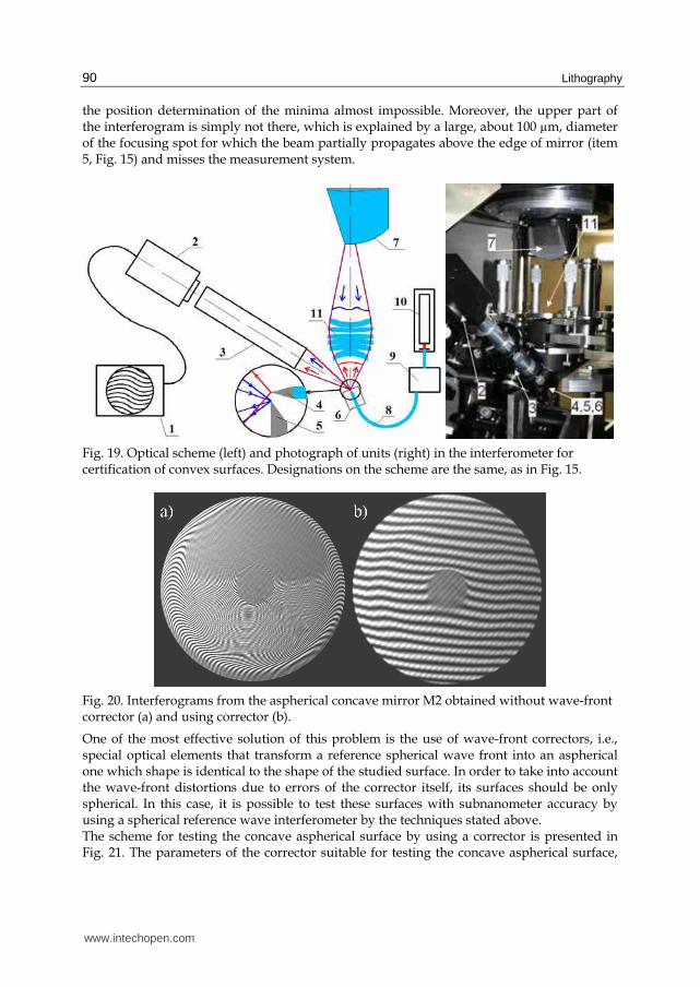
Lithography
90
the position determination of the minima almost impossible Moreover the upper part of the interferogram is simply not there which is explained by a large about 100 microm diameter of the focusing spot for which the beam partially propagates above the edge of mirror (item 5 Fig 15) and misses the measurement system
Fig 19 Optical scheme (left) and photograph of units (right) in the interferometer for certification of convex surfaces Designations on the scheme are the same as in Fig 15
Fig 20 Interferograms from the aspherical concave mirror М2 obtained without wave-front corrector (a) and using corrector (b)
One of the most effective solution of this problem is the use of wave-front correctors ie special optical elements that transform a reference spherical wave front into an aspherical one which shape is identical to the shape of the studied surface In order to take into account the wave-front distortions due to errors of the corrector itself its surfaces should be only spherical In this case it is possible to test these surfaces with subnanometer accuracy by using a spherical reference wave interferometer by the techniques stated above The scheme for testing the concave aspherical surface by using a corrector is presented in Fig 21 The parameters of the corrector suitable for testing the concave aspherical surface
wwwintechopencom
Manufacturing and Investigating Objective Lens for Ultrahigh Resolution Lithography Facilities
91
ie radii of the surfaces thickness and the distance from the reference wave source to the top of the first surface were calculated by minimizing the difference of longitudinal aberrations of the tested aspherical surface and the corrector described in (Malacara 1992 Puryaev 1976) in detail The calculated root-mean-square deviation of the wave front after the corrector from the investigated aspherical shape was RMS=λ1810 This suffices for testing the mirror surface of a nanolithographer with a double-mirror objective It is clearly seen from Fig 20 b) that the interferogram from the aspherical surface obtained by using such a corrector can be reliably processed
Fig 21 Optical scheme (left) and photograph of units in interferometer (right) for certification of concave aspherical surfaces using corrector 1 - computer 2 - registering system 3 - observation system 4 - spherical wave source 5 - flat mirror 6 - 3D precision table 7 - investigated concave aspherical surface 8 - optical fiber 9 - polarization controller 10 - laser 11 - corrector
The analysis of the influence of misalignment in the measurement optical scheme and a thickness error of the compensator on ldquoasphericityrdquo of the wave-front passing through the corrector and accordingly on the measurement accuracy has shown that the requirements for these characteristics of the optical scheme are easily performed in practice In particular the error of a compensator thickness within the limits of plusmn01 mm leads to a wave front aberration at the level of λ1000 Studying of the convex aspherical surfaces is complicated by the fact that besides the corresponding transformation of a spherical front into an aspherical one the corrector must provide a converging front of the wave All of these essentially complicate both the calculation and the design of the corrector In particular in some cases it is necessary to use aspherical surfaces or more than one lens In the case of optics for Schwarzschild objectives this problem is solved easily enough As a corrector the mating concave aspherical mirror which surface has been preliminary tested by using the corrector system described above and corrected according to the procedure described in the next section can be used The measurement scheme is presented in Fig 22 This scheme can be applied for the final
wwwintechopencom
Lithography
92
adjustment and certifications of the objective It is noteworthy to mention that this method can be applied for a convex spherical surface characterization too besides using additional objectives as it is shown in Fig 19
Fig 22 Measurement scheme of aspherical convex mirror М1 using mirror M2 as a wave-front corrector 1 - computer 2 ndash CCD camera 4 - spherical wave source 9-polarization controller 10 ndash laser 11 ndash Schwarzschild objective М1 and М2 ndash convex and concave aspherical mirrors
The measurement accuracy provided by the interferometer depends on many factors including the quality of the reference-wave source the accuracy of determining the positions and a number of interference minima and the accuracy of mathematical retrieval of the surface (wave-front) shape using a limited number of experimental points and the number and degree of the polynomials In turn the accuracy of determining the minimum positions is strongly dependent on the width of the interference pattern the degree of pollution of the interference pattern by ldquoparasiticrdquo interference the method of its rejection the uniformity and intensity of the interfering fronts and a number of other unmanageable factors In this work the interferometer measurement precision was evaluated by studying the rotations of the measured surface maps corresponding to the physical turn of the tested detail The idea of this method is the following If the interferometer provides zero-error measurements then when the detail is rotated the measured surface map should turn correspondingly and the measured statistical parameters of the surface shape deformations should remain unchanged The measured surface deformation maps of a spherical substrate with a numerical aperture NA=014 corresponding to different rotations of the detail are
wwwintechopencom
Manufacturing and Investigating Objective Lens for Ultrahigh Resolution Lithography Facilities
93
presented in Fig 23 The figures demonstrate that the turn of the maps is well observed and the statistical parameters of the deformations change within the limits of RMS=307plusmn0055 nm This test confirms the high measurement accuracy provided by the interferometer which is sufficient for many lithographic applications
Fig 23 Maps and statistical parameters of the surface form deformation corresponding to rotations of the spherical mirror by 0 90 180 and 270 degrees
To summarize this section it is possible to ascertain that the developed interferometer with the diffraction reference wave provides a precision certification of the high-aperture optical surfaces and systems to the subnanometer accuracy
7 Shape correction of optical surfaces to subnanometer accuracy
The developed precise techniques for measuring the shape of optical surfaces made it possible to pass to the main stage the correction of the surface shape made with traditional accuracy λ2 - λ20 depending on the type of optics up to λ1000 - λ2000 In the context of the given work two methods of correction have been developed a vacuum deposition of thin film coatings and ion etching of previously deposited films through metal masks An extremely high accuracy of correcting the surface shape imposes specific requirements on the correction method 1 As a result of the correction process the microroughness of the corrected surface (as a
rule it is initially supersmooth) should remain at the initial level
wwwintechopencom
Lithography
94
2 In the case of a shape correction by means of a local thin film deposition the correcting layers should not distort the substrate surface shape due to intrinsic stress ie they should have a minimally possible stress
3 The correction method should provide the deposition or the removal of materials in a wide range of thickness (1-300 nm) with the accuracy not worse than several percents This problem is especially urgent in the last correction stages when the thickness of the layers to be deposited (removed) is about one nanometer
4 The film materials should allow their complete removal from the substrate (for example chemically) without changing the initial surface shape and microroughness It allows repeating the correction process in the case when the previous correction attempt failed
Researches on stress compensation in multilayer structures and on a substrate restoration have shown that a material meeting all these requirements is CrSc multilayer structure (Salashchenko 2001) The deposition of coatings was made by the magnetron sputtering method The scheme of the correction process and the photograph of the installation are shown in Fig 24 Vacuum in the chamber was (07-1)middot10-6 Tor pressure of working gas (argon) was (07-09)middot10-4 Tor The characteristic power on DC magnetrons was 300-400 W The film thickness control of the deposited layers is performed by variating the passage speed of the corrected surface above the magnetrons sources The stabilization of the discharge power and the argon pressure were provided at the level of 01 The predetermined distribution of the layer thickness over the substrate surface was reached due to the application of figured diaphragms mounted between the magnetron sources and the substrate In addition the substrate rotates around its axis Local values of the film thicknesses over the substrates were measured with an x-ray reflectometer at 447 nm wavelength The details of these measurements will be shown below
Fig 24 Photograph of a technological facility and scheme of surface shape correction by means of multilayer film deposition through masks
The operational experience with this technology has shown a number of important advantages Firstly the roughness of the film surface practically does not depend on the angle of incidence of the atoms in respect to the substrate that allows to carry out the
wwwintechopencom
Manufacturing and Investigating Objective Lens for Ultrahigh Resolution Lithography Facilities
95
correction procedure at normal angles It reduces shadows on the surface increasing the localness of the correction correspondingly Secondly the high accuracy of the layer thickness control up to 1 provides a high reproducibility of the process The film-correction method proved to be efficient for initial stages in which the layers with of tens-hundreds nanometers are deposited in a single correction The process becomes unstable as the thickness of deposited layers decreases down to the units of nanometers Correcting films have changed the proper color that is connected with films oxidation at initial stages of deposition The distribution of oxygen in depth of scandium film obtained with the help of a secondary ion mass-spectroscopy (Drozdov et al 2009) is given in Fig 25 The figure shows an increased content of oxygen on the film surface and at the film-substrate interface Other serious disadvantages of the thin-film-correction method has a discrete and iterative character of the process After each iteration it is necessary to vent the vacuum chamber to make a new diaphragm to pump the chamber again All this strongly decreases the throughput of the process
Fig 25 The distribution of oxygen in depth of scandium film deposited onto Si-substrate
Therefore the application of ion-beam etching at the final correction stage looks very attractive This method allows in particular when focused ion-beams are used to realize the ldquomasklessrdquo correction without frequent opening of the installation to atmosphere Now this method is widely used for substrate form correcting and even for final ion-beam polishing in optical industry (Allen et al 1991 Chason amp Mayer 1993 Ghigo et al 2007) Recently an intensive literature has evolved which is devoted to the application of this method for the precision correction of substrates for projection EUV lithography (Dinger et al 2000 Murakami 2007) For the ion beams applied for the surface shape correction of substrates for EUV and soft X-ray optical elements a number of requirements are imposed the basic of which is the preservation of the surface roughness at an initial (supersmooth) level even when the removed layer depth reaches a few hundreds of nanometers Therefore an optimization of ion energy and incidence angles of the ions on the corrected surface at different depths of material removal is an actual problem Other problems inviting a further investigation are connected with some features of the ion-beam etching at an extremely small depth (asymp 1 nm) removal of materials The experiments have been performed on the installation (Fig 26) with the Cauphmanraquo type ion-beam source KLAN-103M (Website Platar Company 2009) The basic advantage of
wwwintechopencom
Lithography
96
this source is the possibility of working with small ion energies Еi = 50- 300 eV at a significant current density
Fig 26 Photographs of installation for substrates surface shape correction by ion-beam etching
The main characteristics of the ion source are the operating gas is argon or other inert gases the maximal diameter of the ion beam is 100 mm the maximal ion current is 100 mA the maximal ion current density is up to 23 mAcm2 the range of ion energy regulation is 50-1500 eV at the energy spread of plusmn3 eV the discharge working voltage is 35-50 V the thermo-cathode is made of thoriated tungsten (03 mm in diameter) filament Presence of charge-neutralizer (additional thermo-cathode) allows compensating the ion beam charge that provides using the ion source for correction substrates of dielectric materials too The measured dependence of the etching rate of CrSc coating on the removal depth taken at ion energy Еi=200 eV and grazing incidence angle of θ = 42ordm is shown in Fig 27 by dots It is evident that at the initial stage of the etching the removal is less than 120 nm practically a linear increase of the etching rate from the removal depth is observed At a very small etching depth h lt10 nm a wide scatter of the etching rate values is observed Considering the data of the secondary ion mass-spectrometry Fig 28 such a behavior of the etching rate can be explained by oxidation of the sample surface The etching rate of the oxide layer is significantly lower as compared with pure CrSc material If take this into account the calculated etching rate a solid line in Fig 27 matches well the experimental data The observed instability of the etching rate at h lt10 nm might be explained by the variation of the oxidized layer depth in various samples When samples were etched by a neutralized beam (stars in Fig 27) no changes of the rate were observed With the increased ion energy up to 300 eV Fig 29 such instability of the etching rate is not observed either According to atomic-force microscopy measurements the surface roughness remained constant at the level of 02 nm down to 400 nm removal depths For the ion energy of Еi=300 eV when the etching depth exceeds 80 nm an increase of surface roughness is observed (Fig 30)
wwwintechopencom
Manufacturing and Investigating Objective Lens for Ultrahigh Resolution Lithography Facilities
97
Fig 27 Dependence of etching rate on removal depth of CrSc multilayer structures dots are experiment with ions stars are experiment with neutrals and line is calculation accounting etching of the oxidized layer Ion energy Еi = 200 eV and current Ii=60 mA
0 5 10 15 20 25 30 35 40 4500
40x104
80x104
12x105
16x105
Oxigen
SIM
S in
ten
sit
y a
u
Depth nm
Fig 28 Typical distribution of oxygen atoms on depth of CrSc multilayer structure taken by secondary ion mass-spectrometry
The dependences of etching depth on an ion dose (the dose is the product of ion current and etching time) both from the ion current at fixed time and from the time at fixed current show a good linearity that is useful from the practical point of view because it allows to easily define the necessary etching time at a given ion current The example of the dependences of the etching depth on the dose is given in Fig 31 The dashed line corresponds to the linear approximation of the dependence and line with squares represents the experimental data It should be noted that the experiments carried out with greater ion energies up to Ei=15 keV have shown a fast growth of the surface roughness even at small nearby 20ordm grazing angles of incidence of the ions on the surfaces (Chkhalo et al 2008)
wwwintechopencom
Lithography
98
Fig 29 Dependence of ion etching rate on etching depth of CrSc multilayer structures at ion energy Еi = 300 eV (area of small removal depths)
Fig 30 Dependence of surface roughness of CrSc multilayer structures on etching depth at sputtering by argon ions with energy Еi = 300 eV
Fig 31 Dependence of etching depth of the CrSc multilayer structures on ions doze at ion energy Еi = 300 eV - - - linear approximation of the dependence
0 20 40 60 80 1000
10
20
30
40
Etc
hin
g d
ep
th n
m
Dosage mAmin
wwwintechopencom
Manufacturing and Investigating Objective Lens for Ultrahigh Resolution Lithography Facilities
99
For correcting the surface shape of substrates for imaging X-ray optics when the subnanometer form accuracy is required the following strategy providing minimal time expenses has been chosen At the initial stage when peak-to-valley values (P-V) of the surface shape are 50-200 nm the local deposition of the thin films is applied Then at the reduction of the P-V values down to 10-20 nm the ion beams with the energy of 200 eV are used At the final correction stage the 300 eV-ions are applied Figure 32 illustrates the result of using this correction procedure for a spherical substrate with a numerical aperture of NA=025 (the diameter is 130 mm and the curvature radius is 260 mm) which was initially the standard etalon for a conventional interferometer The initial surface map is shown in Fig 32 a) The parameters of the surface were P-V=426 nm and RMS=73 nm The surface shape improved to P-V=73 nm and RMS=06 nm (Fig 32 b)) Thus a root-mean-square deviation of the initial surface shape from an ideal sphere has decreased in 12 times ie in units of the interferometer working wavelength (=0633 microm) it has became better than λ1000 The photograph of this mirror mounted on a metal frame is given in Fig 33
Fig 32 Maps of deviations of the spherical surface shape from the nearest ideal sphere a) initial shape (P-V=426 nm RMS=73 nm) b) after 12-th correction (P-V=73 nm RMS=06 nm)
Fig 33 Photograph of the multilayer spherical mirror for 135 nm wavelength in the frame Diameter of the working aperture is 130 mm
wwwintechopencom
Lithography
100
In spite of a greater wavelength of the traditional deep ultraviolet lithography (193 nm) because of a great number of lens and high requirements for the quality of the projective objectives the methods of correction and certification with a subnanometer accuracy described in this article are urgent for the refracting optics too In connection with this the researches on etching of fused quartz surfaces by ion beams with a compensated charge have been carried out As well as in the case of metal surfaces the main attention was given to the etching rate to the reproducibility of the etching process and to the surface microroughness depending on the beam characteristics incidence angles and material removal depths In Fig 34 the dependences of quartz etching depth on the etching dose are presented The dashed lines in the figure correspond to linear approximations of the dependencies The ion energy was 200 and 300 eV the grazing incidence angle was 42ordm The comparison with similar dependences for CrSc Fig 31 shows that the etching rate of fused quartz is almost twice as much No nonlinearity at the initial stage of the etching is observed that on the one hand proves the hypothesis about the effect of the oxide layer in the case of CrSc material and on the other hand essentially facilitates the correction process
0 100 200 300 4000
50
100
150
200
250
300
350
Etc
hin
g d
ep
th n
m
Dosage mAmin
Fig 34 Dependences of the etching depth on the doze for fused quartz Etching is performed by argon ions with compensated charge and with energy Еi = 200 and 300 eV - - - - linear approximation of dependences
The data on the surface roughness of a fused quartz substrate etched by ions (neutrals) with energies of 200 and 300 eV for various removal depths measured by means of the atomic-force microscope and by x-ray diffractometry are presented in table 1 The substrates manufactured by General optics (USA) were used in the experiment The minimal roughness of initial surfaces measured with an atomic-force microscope was 013 nm and with the x-ray reflection it was about 04 nm From the table it is evident that atomic-force microscope measurements have shown a weaker influence of the etching process on the surface roughness in comparison with the roughness measurements made by the x-ray diffractometry method A more detailed discussion of this difference is beyond the given article Thus the presented experimental data show that these technologies of vacuum deposition and ion-beam etching in the aggregate allow to correct with a subnanometer accuracy the surface shape of optical elements practically of any materials (metals dielectrics semiconductors) with keeping the surface on a supersmooth level This technology is
wwwintechopencom
Manufacturing and Investigating Objective Lens for Ultrahigh Resolution Lithography Facilities
101
suitable for manufacturing elements for imaging x-ray optics and for high resolution systems in visible and deep ultra-violet ranges
Table 1 Roughness of fused quartz substrates depending on neutral (ion) energy and etching depths measured by atomic-force microscopy (AFM) and x-ray diffractometry (X-ray) methods
8 Reflecting multilayer interference mirrors
The final stage of manufacturing a precise mirror for ultrahigh resolution imaging x-ray optical systems is the procedure of the deposition of multilayer reflecting coating on a substrate A low polarizability of materials (le1) and correspondingly a small jump of the refraction factor Δn=00001-01 on the vacuum-material interface and a strong absorption of the radiation by all materials completely exclude the application of refractive optics in the extreme ultra-violet and soft x-ray ranges Because of a low reflection from one interface the reflection optics of normal incidence can be only interferential and the number of layers demanded for the achievement of a high reflectivity depending on a wavelength can reach a value of 102-103 The absorption of the radiation in multilayer structures leads to the fact that the reflectivity is always less than unity While choosing an optimal pair of materials providing a maximal reflectivity on a given wavelength the circumstance is often used that in the range of wavelengths directly adjoining the absorption edge of the material gt AE (AE is the wavelength of the material absorption edge) and coinciding with an anomalous dispersion of the optical constants the lowest absorption and the maximal polarizability of materials are observed For some materials in the field of K-and L- absorption edges the refraction factor can even exceed unity In Fig 35 the calculated spectral dependences of the maximal reflection coefficients for the most attractive pairs of materials in a spectral range of 3 - 16 nm representing the biggest interest for projection nanolithography and high resolution x-ray microscopy are shown The greatest experimental reflectivity about 70 was obtained at a wavelength of 135 nm The spectral range around λasymp67 nm (area of boron anomalous dispersion) is of interest for projection x-ray lithography However the reflectivity obtained here with LaB4C multilayer mirrors at a normal angle of incidence does not exceed 45-47 (Andreev et al 2009) that is not enough for lithographic applications
wwwintechopencom
Lithography
102
2 3 4 5 6 7 8 9 10 11 12 13 14 15 1600
01
02
03
04
05
06
07
08
CrSc
CrC
LaB
MoBe
MoSi
experiment
Refle
ctivity
Wavelength nm
Fig 35 Calculated (lines with symbols) and experimental (stars (Website ESRF 2006 Andreev et al 2003)) reflection coefficients of mostly attractive pairs of materials in X-ray and EUV ranges
On the short-wave length side the working wavelength of the normal incidence multilayer optics is limited by technology capabilities for depositing high-quality short period multilayer structures At present the shortest periods have multilayer structures based on WB4C (the period dasymp1 nm) (Vainer et al 2006 Platonov 2002) and CrSc (dasymp15 nm) (Salashchenko amp Shamov 1997 Website ESRF 2006) A number of special requirements are imposed on the multilayers which should be deposited onto substrates for imaging optics In particular to provide a constructive interference of the waves reflected from different interfaces the radiation wavelength λ the local angle of incidence ( )rθ f
and the period of the multilayer structure ( )d rf should satisfy
the Bragg condition
( )2sin ( )
d rr
λθ=f
f (11)
where rf is a radius-vector of a point of incidence of the radiation on the structure As the
incidence angles are a function of the coordinates it results in the necessity to deposit multilayer structures with a variable over the surface period so-called ldquogradedrdquo structures In some cases for example when the angular divergence of the X-ray beam falling on one point of the mirror surface exceeds the Braggrsquos peak width the multilayer structure should have a variable period on depth (Kozhevnikov et al 2001) One more important feature of multilayer structures for precise optics can be explained as follows For multilayer dispersive elements the maximum deviation of the local value of the period d from the nominal one is determined by the condition of synchronism of the waves reflected from various interfaces which can be expressed through the spectral selectivity of a mirror 1 S d d Nδλ λ δ= = cong (N is a number of periods) In the case of precision multilayer imaging optics when the required surface shape accuracy is at a subnanometer
wwwintechopencom
Manufacturing and Investigating Objective Lens for Ultrahigh Resolution Lithography Facilities
103
level to the synchronism condition an extra requirement for the preservation of the mirror surface shape is added For example for the well-known MoSi multilayer structure optimized on the wavelength of λ=135 nm the period is dasymp7 nm at a number of periods N asymp 40 Correspondingly the general thickness of the structure is L=Nd=280 nm The local error of the period of 1 will affect weakly on reflectivity however the surface shape of the mirror will produce a change of 28 nm which already can essentially produce an influence on imaging properties of the mirror From these simple estimations two important conclusions follow Firstly when designing and manufacturing the surface shape of a substrate it is necessary to take into account the real thickness of a multilayer coating which would be deposited onto the substrate Secondly it is necessary to provide a high at a level of 02-03 accuracy of local values of the period over the mirror surface Besides an intrinsic stress in the multilayer structures which can also deform the surface shape must be taken into account The estimation of the deformation x of a substrate with a diameter D a thickness hsub with the Yung modulus E and the Poisson factor ν on which a hf thick film with the intrinsic stress σ is deposited can be performed by means of equations
2
2
3
4
1
f
sub
h Dx
Y h
EY
σδ
ν
sdot sdot= sdotsdot= minus
(12)
For instance for optimized on maximum of the reflection coefficient MoSi multilayer structure (portion of Mo layer in the period =dMo(dMo+dSi) = 04) the stress in our case is about σ =-350 М『а (Fig 36) At deposition of such a multilayer structure (general thickness is L=Nd=280 nm) on a substrate of fused quartz with the diameter D=220 mm and thickness h=50 mm (Y=844 》а) the maximal deformation of the substrate surface would be about 17 nm that essentially exceeds an admissible level of the surface shape deformation of a mirror for EUV lithography Different groups solve this problem in different ways One the solution is the use of mirrors with a specified thickness ratio of molybdenum layer in the periods Mo asymp 05 - 07 when the stress is close to zero (Windt et al 1994 Zoethout et al 2003) The other solution consists in adding a third material into the periods for example Ru (Oshino et al 2003) However all these methods either because of a stronger absorption of EUV radiation or because of an interface roughness growth have smaller of 10-20 absolute values of the reflectivity In IPM RAS a technique of the stress compensation based on the use of special sublayers lying under the basic MoSi multilayer structure is under development For CrSc multilayer structures the stress is close to zero at γCr=dCr(dCr+dSc)asymp05 (Fig 37 (Andreev et al 2005)) At γCrgt05 a sign of the stress is positive on the contrary to the MoSi structures at γMo= 04 when it is negative The total stress σeff in the structure consisting of CrSc and MoSi multilayer films can be determined from a ratio
( ) ( )
( ) ( )Mo Si Mo Si Mo Si Cr Sc Cr Sc Cr Sc
eff
Mo Si Mo Si Cr Sc Cr Sc
d N d N
d N d N
σ σσ ⎡ ⎤sdot sdot + sdot sdot⎣ ⎦= sdot + sdot (13)
from which it follows that optimizing the composition and the thickness of CrSc layers it is possible to compensate the stress in the basic MoSi reflecting multilayer structure
wwwintechopencom
Lithography
104
Fig 36 Stress in MoSi multilayer structures depending on ratio of Mo layer in period γMo=dMo(dMo+dSi) at fixed period d=697 nm
Fig 37 Stress in CrSc multilayer structure depending on ratio of Cr layer in period γCr=dCr(dCr+dSc) at fixed period d=54 nm
In practice it is necessary to consider a process of the stress relaxation which depending on the structure and materials is variable over several days Totally the stress can change by tens percent An example of such a process is illustrated in Fig 38 in which the time dependencies of the stress in multilayer structures consisting of anti-stress CrSc sublayers and MoSi reflecting layers are presented The structures differ by thicknesses of the sublayers It is necessary to note that the stress value is affected not only by ratio of the layer thickness in the period but also by the period size and conditions in which the films were deposited For depositing multilayer structures a method of magnetron spattering is used in IPM RAS The method allows depositing films onto curved as well as flat substrates The conditions under which multilayer structures are deposited are briefly described in section 6 devoted to the correction of the substrate surface shape by the method of local thin-film deposition The facilities have from two to six magnetron sources that allows depositing at one technological cycle reflecting anti-stress and anti-diffusion barrier layers Now the
σ MP
a
-1000
-800
-600
-400
-200
0
200
400
600
02 04 06 08 10
γMo=dMo (dMo+dSi)
0
100
200
300
400
500
600
700
06 065 07 075
σ MP
a
γCr = dCr (dCr+dSc)
wwwintechopencom
Manufacturing and Investigating Objective Lens for Ultrahigh Resolution Lithography Facilities
105
technologies of depositing more than twenty various pairs of materials are developed It allows manufacturing optics for a whole x-ray and extreme ultra-violet spectral range More details about the properties of the multilayer structures can be found in (Andreev et al 2003)
Fig 38 Stress in MoSi multilayer structures with anti-stress CrSc sublayers versus of time a) - [(CrSc)times42 d=538 nm =067 (MoSi))times45 d=698 nm =04] and b) - [(CrSc)times40 d=538 nm =067 (MoSi)times45 d=698 nm =04]
A great volume of works high requirements for the coating quality and for accuracy of the period distribution over a substrate surface dictate the need for an operative information about characteristics of the deposited coatings with the purpose of correcting the technological process It is most convenient to perform such work with the presence of laboratory reflectometers allowing the investigation of multilayer structures on working wavelengths and located in the immediate vicinity of technologists Therefore laboratory reflectometers are constantly being developed and improved recently In Refs (Loyen et al 2003 Miyake et al 2003 Gulikson et al 1992) the specialized reflectometers for investigating multilayer optics in the range around 135 nm are described As a source of the soft x-ray and EUV radiation the laser plasma is used which arises due to the irradiation of solid-state targets by laser light with a power density about 109 Wcm2 For monochromatization the radiation spherical diffraction gratings operating at grazing angles are used The characteristic fluxes of the photons in the working range of wavelengths of 10-16 nm on the investigated samples with the probe beam size asymp 2 mm are 107 - 108 photons (01 nmtimess) The results of reflectivity measurements of MoSi multilayer mirrors in the area of 135 nm obtained with the help of these reflectometers as compared with the data obtained with a PTB-reflectometer (synchrotron BESSY-2 Berlin Germany which is considered as the reference one) have shown the coincidence of the measured reflection coefficients at a level of 3 and the resonant wavelength asymp 001 nm The basic disadvantages of these reflectometers in our opinion are a narrow range of working wavelengths and a low spectral resolution caused by the applied monochromator scheme The monochromator consists of two stationary slits and spherical (or toroidal) diffraction grating Scanning across the spectrum is carried out due to the diffraction gratings rotation around its axis According to this arrangement the position of the slits and the diffraction grating coincides with the Rowland circle (Rowland 1893) only for one
-30
-20
-10
0
10
20
30
50 100 15 200 250
Time hours
σ eff
MP
a
a)
t days
σ MPa
- 40
- 30
- 20
- 10
0
1 2 3 4 5 6 7 8 9
x
x
xx
x x
b)
wwwintechopencom
Lithography
106
wavelength that essentially limits the range where the spectral resolution of the monochromator is kept at the acceptable level of Δλapp asymp 001-002 nm The other factor limiting working spectral range of the reflectometer is the type of the used radiation source (laser plasma) which large size does not allow scanning by the entrance slit of the grating spectrometer Our group develops multilayer optics for a wide spectral range λ=06-50 nm and the monochromator spectral resolution up to 0003-0005 nm is frequently required Therefore in IPM RAS laboratory reflectometers on the basis of high resolution grating monochromators have been developed These monochromators have a movable entrance slit and diffraction grating (Chkhalo et al 1998 Zuev amp Mitrofanov 2002 Bibishkin et al 2004 Bibishkin et al 2005) In the reflectometrs the monochromators of type RSM-500 (Lukirsky et al 1967) and McPherson-247 (Website Mcpherson Company 2009) are used The photograph and optical scheme of the last generation reflectometer are given in Fig 39 Owing to such a spectrometer the kinematic scheme slits and diffraction grating are always located in the Rowland focusing circle so that the high spectral resolution of the device in the whole range of wavelengths is provided Two diffraction gratings with various radiuses of curvature cover this spectral range
Fig 39 Optical scheme and photograph of the reflectometer XRT - x-ray tube S1 S2 - entrance and exit slits AS VS - horizontal and vertical anti-scattering slits DG - diffraction grating TM - toroidal mirror M ndash probe beam intensity monitor MIS - investigated sample D ndash detector G5 ndash five-axes goniometer
In the reflectometer the radiation from the anode of the x-ray tube (XRT) through the entrance slit of the monochromator (S1) falls on the diffraction grating (DG) The diffracted monochromatic radiation according to the diffraction grating equation cosϕ - cosψ =mλD (m - the order of diffraction λ ndash a wavelength and D - the grating period ϕ and ψ angles of diffraction and incidence correspondingly) is focused onto the spectrometer exit slit S2 Scanning across the spectrum is carried out by linear moving of the diffraction grating and the exit slit with a simultaneous turn of the diffraction grating so that the condition Xl=Rgsdot sinψ where Rg - radius and Xl - distance between the diffraction grating center and the exit slit is satisfied An anti-scattering diaphragm (AS) reduces the intensity of scattered radiation at the output of the monochromator and limits the irradiated area of the diffraction grazing The monochromatic radiation by means of a toroidal mirror (TM) is focused on the investigated sample The other important function of the toroidal mirror is connected with a filtration of higher diffraction orders which is especially urgent when
wwwintechopencom
Manufacturing and Investigating Objective Lens for Ultrahigh Resolution Lithography Facilities
107
working with bremsstrahlung of the tungsten anode Radiuses of the toroidal mirror are chosen in such a way that in a horizontal plane the exit slit and in a vertical plane the source are imaged on the sample under study The studied sample is installed on a five-axis goniometer which photograph and scheme of movements are shown in Fig 40 The linear translation along X and Z axes the rotation around them (ω and ) and the inclination θ allow to insert any point of the sample under study with a diameter up to 300 mm into the x-ray beam The detector executes 2 rotation The additional inclination of the detector 2θ allows to increase the numerical aperture of the sample which can be tested up to NA=05
Fig 40 Photograph of the goniometer and scheme of movements provided by the goniometer
The concept of a spectrometer-monochromator with a movable slit and diffraction grating became possible only due to the application of the dismountable x-ray tube of an original design as the radiation source The advantages of classical sealed x-ray tubes are their small dimensions and weight simplicity in operation sufficient for reflectometric applications intensity of the x-ray radiation and long life-time However the application of these sources for precision reflectometry in soft x-ray and extreme ultra-violet ranges has shown that because of the fast contamination of the anode by products of thermocathode material erosion and hydrocarbons decomposition under a powerful electron-beam emission characteristics and life-time of the tubes collapsed when comparing with expected values For solving this problem in our work the tube was equipped with an ion-beam source for cleaning anodes from contaminations (Bibishkin et al 2003) It allows to work without opening the spectrometer and the tube to the atmosphere within several months thus approaching its operation mode to the traditional sealed X-ray tubes for hard X-rays The work is done on K L and M characteristic lines of target (anode) materials and on continuous bremsstrahlung spectrum of tungsten On one holder about 8 targets of various materials are installed It is necessary to note that frequently it is possible to use a few spectral lines from one target
wwwintechopencom
Lithography
108
As an illustration in Fig 41 the measured spectral dependence of reflectivity of MoSi multilayer spherical mirror shown in Fig 40 is presented The measurement has been performed with the reflectometer at an incidence angle of the radiation to the sample of 5ordm (from the local normal)
Fig 41 Spectral dependence of the reflection coefficient of MoSi multilayer mirror deposited onto spherical substrate Angle of incidence was 5ordm from the local normal
One more important advantage of the x-ray tube as a source of X-ray radiation is that in the field of wavelengths lt3 nm because of aberrations of spherical grating the spectral width of the probe beam is ΔGge 001 nm while the spectral resolution of short period multilayers reaches values Δ MIS lt001 nm Since the natural width of characteristic lines of some materials in this range is essentially less than this value this circumstance provides precision measurements of reflective characteristics of multilayer mirrors even when monochromator does not provide the demanded resolution Thus the developed in IPM RAS methods of multilayer coating deposition stress compensation in the film structures laboratory metrology of the mirrors at working wavelengths restoration of the substrates without any damage of the substrate surface shape and roughness allow us to make and certify high reflecting multilayer mirrors with a sub-nanometer level surface shape accuracy attended for super-high resolution imaging X-ray optics
9 Conclusion
In the given article the basic researches and the full cycle of developed in IPM RAS technologies and metrology techniques from the substrate surface shape correction to the deposition of multilayer coatings on them which are required for manufacturing high reflecting mirrors for diffraction quality imaging in the extreme ultra-violet and in the soft X-ray ranges are described As a whole it is evident that the problem of manufacturing such optics for high resolution EUV lithography and X-ray microscopy is already solved as a first approximation The further activity should be directed toward the increase of both in manufacturing accuracy of optical surfaces up to a level of RMS=01 nm and in the numerical aperture of objectives up to NA=04-06
0
10
20
30
40
50
60
70
126 130 134 138 142
Wavelength nm
Refl
ect
ivit
y
wwwintechopencom
Manufacturing and Investigating Objective Lens for Ultrahigh Resolution Lithography Facilities
109
In this connection upgrading the interferometric methods for surface shape measurements of optical elements and wave-front deformations of objectives first of all and regarding the increase of their working numerical aperture is a subject of current interest The diffraction interferometers utilizing the tipped fiber as a source of the reference spherical wave look rather attractive Owing to the simplicity of the design high intensity of the diffracted wave weak sensitivity to the adjustment in an optical circuit and a number of other advantages the interferometers which are simple in operation can be developed for the optical industry In the framework of the given article the problem arising when aspherical surfaces are under investigation of development and optimization of correctors transforming the reference spherical fronts into the aspherical ones which shapes are identical to the shapes of the studied surfaces was not practically discussed Meanwhile traditional lens null-correctors have limited capabilities rather complicated in manufacturing and expensive and demand complicated calibrating procedures for taking into account the wave-front distortions due to errors of the corrector itself In this connection diffraction correctors represent a significant interest (Akatov et al 2004) A gross potential for the surface shape correction of dielectric materials by means of ion-beams has RF-etching in chemically active environments The first experiments on etching of quartz substrates by means of the RF-etching have shown that the surface micro-roughness did not change down to the removal depths of a few micrometers (Akhsakhalyan et al 2008) The most serious problem on the way of manufacturing the effective optics for the soft X-ray radiation λlt10 nm is that reflection coefficients of the multiplayer mirrors are not sufficiently high Nevertheless the results that have been recently obtained in the field of the X-ray optics teams may be considered as a break-through because they lay the foundation of developing such important physico-technological directions as projection EUV nanolithography X-ray microscopy and extraterrestrial astronomy of the ultrahigh resolution
10 References
Akhsakhalyan AD Vainer YuA Volgunov DG Drozdov MN Kluenkov EB Kuznetcov MI Salashchenko NN Kharitonov AI amp Chkhalo NI (2008) Application of reactive ion-beam etching for surface shape correction of X-ray mirrors Proceedings of Workshop ldquoX-ray optics ndash 2008rdquo pp 26-28 Chernogolovka Moscow region 6-9 October 2008 p 26-28 IPTM Chernogolovka (in Russian)
Allen LN Keim RE amp Lewis TS (1991) Surface error correction of a Keck 10 m telescope primary mirror segment by ion figuring Proceedings SPIE Vol 1531 1991 pp 195ndash204
Andreev SS Bulgakova SA Gaponov SV Gusev SA Zuev SYu Kluenkov EB Luchin VI Lopatin AYa Mazanova LM Prokhorov KA Sadova EN Salashchenko NN amp Shamov EA (2000) Investigations in field of projection lithography of extreme ultraviolet region in Institute for physics of microstructures RAS Surface X-ray synchrotron and neutron investigations Vol 1 2000 pp 32-41 (in Russian)
Andreev SS Akhsakhalyan AD Bibishkin MS Chkhalo NI Gaponov SV Gusev SA Kluenkov EB Prokhorov KA Salashchenko NN Schafers F amp Zuev
wwwintechopencom
Lithography
110
SYu (2003) Multilayer optics for XUV spectral region technology fabrication and applications Central European Journal of Physics Vol 1 2003 pp 191-209
Adreev SS Kluenkov EB Misinov AL Polkovnikov VN Salashchenko NN Suslov LA amp Chernov VV (2005) Compensation of elastic deformation of MoSi multilayer structures on quartz and zerodur substrates using buffer CrSc technique Surface investigations Vol 2 2005 pp 45-48 (In Russian)
Andreev SS Barysheva MM Chkhalo NI Gusev SA Pestov AE Polkovnikov VN Salashchenko NN Shmaenok L A Vainer YuA amp Zuev SYu (2009) Multilayered mirrors based on LaB4C(B9C) for x-ray range near anomalous dispersion of boron ( near 67 nm) Nuclear Instruments and Methods in Physics Research SecA Vol 603 2009 pp 80-82
Archer KM (1997) Craniofacial reconstruction using hierarchical b-spline interpolationrdquo A thesis submitted in partial fulfilment of the reguirements for the degree of master of applied science The university of British Columbia 1997 p 113
Asadchikov VE Kapabekov AYu Kozhevnikov IV Levashov VE amp Sagitov SI (1998) Experimental investigation of roughness correlation of a film and a substrate by means of X-ray scattering Crystallography Vol 43 No 1 1998 pp 119-130 (In Russian)
Barbee TW (Jr) (1981) Sputtered layered synthetic microstructures (LSM) dispersion elements Proceedings of Conference ldquoLow energy X-ray diagnosticsrdquo pp 131-145 Monterey USA 1981 N Y Amer Inst Phys
Benschop JPH Kaiser WM amp Ockwell DC (1999) EUCLIDES the European EUVL program SPIE Symposium on Micro-lithography Vol 3676 1999 p 246
Bibishkina MS Zabrodin IG Klyuenkov EB Salashchenko NN Chekhonadskih DP amp Chkhalo NI (2003) A new dismountable tube for soft X-ray radiation Surface investigations No 2 2003 pp 41-45 (In Russian)
Bibishkinb MS Zuev SYu Salashchenko NN amp Chkhalo NI (2003) Measuring of microroughness of surfaces using soft X-ray radiation Surface investigations No 1 2003 pp 94-96 (In Russian)
Bibishkin MS Chekhonadskih DP Chkhalo NI Klyuenkov EB Pestov AE Salashchenko NN Shmaenok LA Zabrodin IG amp Zuev SYu (2004) Laboratory methods for investigation of multilayer mirrors in Extreme Ultraviolet and Soft X-Ray region Proceedings of SPIE Vol 5401 2004 pp 8-15
Bibishkin MS Vainer YuA Pestov AE Prokhorov KA Salashchenko NN Fraerman AA amp Chkhalo NI (2005) Investigation of characteristics of multilayer X-ray mirrors with ultra-short periods d = 07-24 せす Bulletin of the Russian Academy of Sciences Physics Vol 69 No 2 2005 pp 199-206
Blunt R (2006) White light interferometry - a production worthy technique for measuring surface roughness on semiconductor wafers Proceedings of CEMANTECH Conference pp 59-62 Vancouver Canada April 24-27 2006
Born M amp Wolf E (1973) Principles of optics second edition Science Moscow (In Russian)
Braat J (1987) Polynomial expansion of severely aberrated wave fronts Optical Society of America Vol 4 No 4 1987 pp 643-650
Chason E amp Mayer T M (1993) Low energy ion bombardment induced roughening and smoothing of Si02 surfaces Applied Physics Letters Vol 62 No 4 1993 pp 363-365
Cheng P (1987) Instrumentation and Biological Applications In X-ray Microscopy Springer Verlag
wwwintechopencom
Manufacturing and Investigating Objective Lens for Ultrahigh Resolution Lithography Facilities
111
Chkhalo NI Dolbnya IG Fedorchenko MV Kruglyakov EP Zarodyshev AV amp Zolotarev KV (1993) Multilayer mirror on copper-nickel substrates for intense X-ray beams Proceedings of the 4-th International Conference ldquoX-Ray Microscopy 4rdquo pp 586-592 Russia Chernogolovka September 20-24 1993 IPTM Chernogolovka
Chkhalo NI Fedorchenko MV Kruglyakov EP Volokhov AI Baraboshkin KS Komarov VF Kostyakov SI amp Petrov EA (1995) Ultradispersed diamond powders of detonation nature for polishing X-ray mirrors Nuclear Instruments and Methods in Physics Research A Vol 359 1995 pp 155-156
Chkhalo NI Kirpotin AN Kruglyakov EP amp Semenov EP (1998) Reflectometer for precision tests of optical components in the ultrasoft X-ray range Nuclear Instruments and Methods in Physics Research A Vol 405 1998 pp 393-395
Chkhaloa NI Raskin DG amp Salashchenko NN (2008) Capabilities of microinterferometer with digital recording of images for studying micro-objects with sub-nanometer resolution Proceedings of SPIE Vol 7025 2008 p 702512
Chkhalob NI Dorofeyev IA Salashchenko NN amp Toropov MN (2008) A plane wave diffraction on a pin-hole in a film with a finite thickness and real electrodynamic properties Proceedings of SPIE Vol 7025 2008 p 702506
Chkhaloc NI Klimov AYu Rogov VV Salashchenko NN amp Toropov MN (2008) A source of a reference spherical wave based on a single mode optical fiber with a narrowed exit aperture Rev Sci Instrum Vol 79 2008 p 033107
Chkhalod N Paramonov L Pestov A Raskin D amp Salashchenko N (2008) Correction of the EUV mirror substrate shape by ion beam Proceedings of SPIE Vol 7025 2008 p 702503
Dinger U Bisert F Lasser H Mayer M Seifert A Seitz G Stacklies S Stickel F-J amp Weise M (2000) Mirror substrates for EUV-lithography progress in metrology and optical fabrication technology Proceedings of SPIE Vol 4146 2000 pp 35ndash46
Dorofeyev I Jersch J amp Fuchs H (2003) Spectral composition of electromagnetic fluctuations induced by a lossy layered system Annalen der Physik Vol 12 No 7-8 2003 pp 421-437
Dorofeev I (2009) Amplitude-phase characteristics of electromagnetic fields diffracted by a hole in a thin film with realistic optical properties Physica E Vol 41 2009 pp 762-770
Drozdov MN Drozdov YuN Barysheva MM Polkovnikov VN amp Chkhalo NI (2009) Minimization of matrix effects upon layer-by-layer analysis of multilayer metallic nanostructures LaB4C by SIMS using cluster secondary ions Proceedings of Symposium ldquoNanophysics and nanoelectronicsrdquo Vol 1 pp 190-191 Nizhniy Novgorod Russia 16-20 March 2009 IPM RAS Nizhniy Novgorod (in Russian)
Gavrilin DA (2003) Investigations of methods for shape description of complicated optical surfaces at interferometrical control PhD thesis St-Petersburg Russia 103 p (in Russian)
Ghigo M Canestrari R Spiga D amp Novi A (2007) Correction of high spatial frequency errors on optical surfaces by means of Ion Beam Figuring Proceedings of SPIE Vol 6671 2007 p 667114
Goldberg KA amp Kevin G (2001) Wave-front measurement errors from restricted concentric subdomains J Opt Soc Am A Vol 18 No 9 2001 pp
wwwintechopencom
Lithography
112
Goldberg KA Naulleau P Bokor J Chapman HN amp Barty A (2002) Testing extreme ultraviolet optics with visible-light and extreme ultraviolet interferometry J Vac Sci Technol B Vol 20 No 6 2002 pp 2834-2839
Griffith J E amp Grigg DA (1993) Dimensional metrology with scanning probe microscopes Journal of Applied Physics Vol 74 1993 pp R83-R109
Gullikson EM Underwood JH Batson PC and Nikitin V (1992) A soft X-rayEUV reflectometer based on a laser produced plasma source Journal of x-ray science and technology Vol 3 1992 pp 283-299
Gwyn C (1998) White paper on Extreme ultraviolet Lithography Proceedings of EUV LLC 1998 Livermore
Klimov AYu Rogov VV Salashchenko NN amp Chkhalo NI (2008) A Spherical Wave Source Based on a Probe for a Near-Field Microscope Bulletin of the Russian Academy of Sciences Physics Vol 72 No 2 2008 pp 204-206
Kluyenkova EB Pestov AE Polkovnikov VN Raskin DG Toropov MN Salashchenko NN amp Chkhalo NI (2008) Testing and Correction of Optical Elements with Subnanometer Precision Nanotechnologies in Russia Vol 3 Nos 9-10 2008 pp 602-610
Klyuenkovb EB Polkovnikov VN Salashchenko NN amp Chkhalo NI (2008) Shape Correction of Optical Surfaces with Subnanometer Precision Problems Status and Prospects Bulletin of the Russian Academy of Sciences Physics Vol 72 No 2 2008 pp 188-191
Kozhevnikov IV Asadchikov VE Duparre A Gilev ON Havronin NA Krivonosov YuS Ostashev VI amp Steinert J (1999) Comparative study of the roughness of optical surfaces and thin films using atomic force microscopy x-ray scattering and light scattering methods Proceedings of SPIE Vol 3739 1999 pp 348-354
Kozhevnikov IV Bukreeva IN amp Ziegler E (2001) Nuclear Instruments and Methods in Physics Research Sec A Vol 460 2001 p 424
Linnik VP (1933) A simple interferometer to test optical systems Bulletin of the Academy of Science of the USSR Vol 1 1933 pp 210-212
Loyen L Bottger T Braun S Mai H Leson A Scholze F Tummler J Ulm G Legall H Nickels PV Sandner W Stiel H Rempel C Schulze M Brutscher J Macco F amp Mullender S (2003) A New Laboratory EUV Reflectometer for Large Optics using a Laser Plasma Source Proceedings of SPIE Vol 5038 2003 pp 12-21
Lukirsky AP Brytov IA amp Komyak NI (1967) Prototype of an X-ray spectrometer with diffraction grating and ionization detection for spectral region of 10-55 Aring Apparatus and methods of X-ray analysis No 2 1967 pp 4-19 L Engineering (in Russian)
Malacara D ed (1992) Optical shop testing 2nd ed John Wiley amp Sons Inc ISBN 0-471-52232-5 New York
Medecki H Tejnil E Goldberg KA amp Bokor J (1996) Phase-shifting point diffraction interferometer Optics letters Vol 21 No 19 1996 pp 1526-1528
Miyake A Miyachi T Amemiya M Hasegawa T Ogushi N Yamamoto T Masaki F amp Watanabe Y (2003) LPP-based reflectometer for characterization of EUV lithography systems Proceedings of SPIE Vol 5037 2003 pp 647-655
Murakami K Saito Y Ota K et al (2003) Development of an experimental EUV interferometer for benchmarking several EUV wavefront metrology schemes Proceedings of SPIE Vol 5037 2003 pp 75-82
wwwintechopencom
Manufacturing and Investigating Objective Lens for Ultrahigh Resolution Lithography Facilities
113
Murakami K Oshino T Kondo H Chiba H Komatsuda H Nomura K amp Iwata H (2007) Development of optics for EUV lithography tools Proceedings of SPIE Vol 6517 2007 pp 65170J
Naulleau PP Goldberg KA Lee SH Chang C Attwood D amp Bokor J (1999) Extreme-ultraviolet phase-shifting point-diffraction interferometer a wave-front metrology tool with subangstrom reference-wave accuracy Appl Opt Vol 38 No 35 1999 pp 7252-7263
Naulleau P Goldberg KA Lee SH Chang Ch Atwood D amp Bokor J (2000) The EUV phase-shifting point diffraction interferometer Synchrotron Radiation Instrumentation Eleventh US National Conference ed by P Pianetta p 66-72 ISBN 1-56396-941-6 American Institute of Physics
Naulleau P Golberg KA Anderson EH et al (2002) Sub-70 nm Extreme Ultraviolet Lithography at the Advanced Light Source Static Microfield Exposure Station Using the Engineering Test Stand Set-2 Optic Jour Vac Sci Technol B Vol 20 2002 pp 2829ndash2833
Nevot L amp Croce P (1980) Characterisation des surfaces par reflection rasante de rayon Application a lrsquoetude du polissage de quelque verres silicates Revue de Physique Appliquee Vol 15 1980 pp 761-779
Okatov MA Antonov EA Baigozhin A et al (2004) Handbook for optical-technologist St- Petersburg Politechnica 2004 679 p
Oshino T Shiraishi M Kandaka N Sugisaki K Kondo H Ota K Mashima K Murakami K Oizumi H Nishiyama I amp Okazaki S (2003) Development of illumination optics and projection optics for high-NA EUV exposure tool (HiNA) Proceedings of SPIE Vol 5037 2003 pp 75-82
Ota K Murakami K Kondo H Oshino T Sugisaki K amp Komatsuda H (2001) Feasibility study of EUV scanners Proceedings of SPIE Vol 4343 2001 pp 60-69
Otaki K Ota K Nishiyama I Yamamoto T Fukuda Y amp Okazaki S (2002) Development of the point diffraction interferometer for extreme ultraviolet lithography Design fabrication and evaluation J Vac Sci Technol B Vol 20 No 6 2002 pp 2449-2458
Palik ED (1985) Hanbook of optical constants of solids Naval Research Laboratory Washington DC 1985 749 pp
Parratt LG (1954) Surface studies of solids by total reflection of x-rays Physical Review Vol 35 1954 pp 359-369
Platonov Yu Gomez L amp Broadway D (2002) Proceedings of SPIE Vol 4782 2002 p 152 Protopopov VV Valiyev KA amp Imamov RM (1999) Measurement of spatial
distribution of superpolished surface roughness and defects in multilayer X-ray mirrors Surface investigations No 1 1999 pp 111-119 (In Russian)
Puryaev DT (1976) Methods for control of aspherical surfaces M Engineering 1976 13 p (in Russian)
Rodionov SA Przhevalinsky LI amp Shekhonin AA (1974) Application of coefficients of interpolation polynomial for optical system aberrations presentation Bulletin of the USSR institutions of higher education Instrument engineering Vol 17 No 10 1974 p 104 (in Russian)
Rodionov SA (1995) Mthematical apparatus for ptics control ndash general approach Optical journal No 8 1995 pp 49-51
Rowland H (1893) Gratings in theory and practice Phil Mag Vol 35 1893 p 397 Salashchenko NN amp Shamov EA (1997) Optics communication Vol 134 1997 p 7
wwwintechopencom
Lithography
114
Salashchenko NN (2001) Optical Element and Method for Recovering the Substrate Patent DE 101 01 820 A1 00074P
Sinha SK Sirota EB Garoff S amp Stanley HB (1988) X-ray and neutron scattering from rough surfaces Physical Rev B Vol 38 No4 1988 pp 2297-2311
Sommargren GE (1996) Diffraction methods raise interferometer accuracy Laser Focus World Vol 8 1996 p 61-71
Soufli R Spiller E Schmidt MA Davidson JC Grabner RF Gullikson EM Kaufmann BB Mrowka S Baker SL Chapman HN Hudyma RM Taylor JS Walton ChC Montcalm C amp Folta JA (2001) Multilayer optics for an extreme ultraviolet lithography tool with 70 nm resolution Proceedings of SPIE Vol 4343 2001 pp 51-59
Stone VW Jonas AM Nysten B amp Legras R (1999) Roughness of free surfaces of bulk amorphous polymers as studied by x-ray surface scattering and atomic force microscopy Physical Rev B Vol 60 No 8 1999 pp 5883-5894
Sun X Chen S amp Shen Q (1998) Geometric calibration of lens using B-spline surface fitting Wuhan University Journal of Natural Sciences Vol 3 No 4 1998 pp 440-442
Swantner W amp Weng W C (1994) Gram-Schmidt orthogonalisation of Zernike polynomials for general aperture shapes Applied optics Vol 33 No 10 1994 pp 1832-1837
Sweeney DW Hudyma RM Chapman HN amp Shafer D (1998) EUV optical design for a 100 nm CD imaging system Proceedings of SPIE Vol 3331 1998 pp 2-10
Underwood JH amp Barbee (Jr) TW (1981) Layered synthetic microstructures as Bragg diffractors for X-rays and extreme ultraviolet theory and predicted performance Appl Opt Vol 20 1981 pp 3027-3034
Vainer YuA Pestov AE Prokhorov KA Salashchenko NN Fraerman AA Chernov VV amp Chkhalo NI (2006) Analysis of Cross-Correlation of Interface Roughness in Multilayer Structures with Ultrashort Periods Journal of Experimental and Theoretical Physics Vol 103 No 3 2006 pp 346-353
Warburton WK Rek ZU amp Barbee (Jr) TW (1987) Quality Investigation of multilayer covers for X-ray optics In X-ray optics and microscopy pp 222-231 World Moscow (In Russian)
Website ESRF httpwwwesrfeueventsconferencespast-conferences-and-workshops pxrms06Detailed-programm12_gulliksonpdf
Website GO Corporation httpwwwgoochandhousegocomproductscat3 Website Mcpherson Company httpwwwmcphersoninccomspectrometers
xuhvvuvuvxuhvvuvuvhtm Website Platar Company httpwwworcru~platarP1Rhtml Website Veeco Instruments httpwwwveecocom Website Zygo Corporation httpwwwzygocom Williamson DM (1995) The elusive diffraction limit OSA Proceedings on Extreme
Ultraviolet Lithography F Zernike and DT Attwood eds Vol 23 1995 pp 68-76 Windt DL Brown WL Volkert CA amp Waskiewicz WK (1994) J Appl Phys Vol 78
1994 p 2423 Zoethout E Sipos G van de Kruijs RWE Yakshin AE Louis E Mullender S amp
Bijkerk F (2003) Stress mitigation in MoSi multilayers for EUV lithography Proceedings of SPIE Vol 5037 2003 pp 872ndash878
Zuev SYu amp Mitrofanov AV (2002) Measurements of parameters of optical elements for X-ray telescopes Surface investigations No 1 2002 pp 81-83 (In Russian)
wwwintechopencom
LithographyEdited by Michael Wang
ISBN 978-953-307-064-3Hard cover 656 pagesPublisher InTechPublished online 01 February 2010Published in print edition February 2010
InTech EuropeUniversity Campus STeP Ri Slavka Krautzeka 83A 51000 Rijeka Croatia Phone +385 (51) 770 447 Fax +385 (51) 686 166wwwintechopencom
InTech ChinaUnit 405 Office Block Hotel Equatorial Shanghai No65 Yan An Road (West) Shanghai 200040 China
Phone +86-21-62489820 Fax +86-21-62489821
Lithography the fundamental fabrication process of semiconductor devices plays a critical role in micro- andnano-fabrications and the revolution in high density integrated circuits This book is the result of inspirationsand contributions from many researchers worldwide Although the inclusion of the book chapters may not be acomplete representation of all lithographic arts it does represent a good collection of contributions in this fieldWe hope readers will enjoy reading the book as much as we have enjoyed bringing it together We would liketo thank all contributors and authors of this book
How to referenceIn order to correctly reference this scholarly work feel free to copy and paste the following
NI Chkhalo AE Pestov NN Salashchenko and MN Toropov (2010) Manufacturing and InvestigatingObjective Lens for Ultrahigh Resolution Lithography Facilities Lithography Michael Wang (Ed) ISBN 978-953-307-064-3 InTech Available from httpwwwintechopencombookslithographymanufacturing-and-investigating-objective-lens-for-ultrahigh-resolution-lithography-facilities
copy 2010 The Author(s) Licensee IntechOpen This chapter is distributedunder the terms of the Creative Commons Attribution-NonCommercial-ShareAlike-30 License which permits use distribution and reproduction fornon-commercial purposes provided the original is properly cited andderivative works building on this content are distributed under the samelicense

Manufacturing and Investigating Objective Lens for Ultrahigh Resolution Lithography Facilities
91
ie radii of the surfaces thickness and the distance from the reference wave source to the top of the first surface were calculated by minimizing the difference of longitudinal aberrations of the tested aspherical surface and the corrector described in (Malacara 1992 Puryaev 1976) in detail The calculated root-mean-square deviation of the wave front after the corrector from the investigated aspherical shape was RMS=λ1810 This suffices for testing the mirror surface of a nanolithographer with a double-mirror objective It is clearly seen from Fig 20 b) that the interferogram from the aspherical surface obtained by using such a corrector can be reliably processed
Fig 21 Optical scheme (left) and photograph of units in interferometer (right) for certification of concave aspherical surfaces using corrector 1 - computer 2 - registering system 3 - observation system 4 - spherical wave source 5 - flat mirror 6 - 3D precision table 7 - investigated concave aspherical surface 8 - optical fiber 9 - polarization controller 10 - laser 11 - corrector
The analysis of the influence of misalignment in the measurement optical scheme and a thickness error of the compensator on ldquoasphericityrdquo of the wave-front passing through the corrector and accordingly on the measurement accuracy has shown that the requirements for these characteristics of the optical scheme are easily performed in practice In particular the error of a compensator thickness within the limits of plusmn01 mm leads to a wave front aberration at the level of λ1000 Studying of the convex aspherical surfaces is complicated by the fact that besides the corresponding transformation of a spherical front into an aspherical one the corrector must provide a converging front of the wave All of these essentially complicate both the calculation and the design of the corrector In particular in some cases it is necessary to use aspherical surfaces or more than one lens In the case of optics for Schwarzschild objectives this problem is solved easily enough As a corrector the mating concave aspherical mirror which surface has been preliminary tested by using the corrector system described above and corrected according to the procedure described in the next section can be used The measurement scheme is presented in Fig 22 This scheme can be applied for the final
wwwintechopencom
Lithography
92
adjustment and certifications of the objective It is noteworthy to mention that this method can be applied for a convex spherical surface characterization too besides using additional objectives as it is shown in Fig 19
Fig 22 Measurement scheme of aspherical convex mirror М1 using mirror M2 as a wave-front corrector 1 - computer 2 ndash CCD camera 4 - spherical wave source 9-polarization controller 10 ndash laser 11 ndash Schwarzschild objective М1 and М2 ndash convex and concave aspherical mirrors
The measurement accuracy provided by the interferometer depends on many factors including the quality of the reference-wave source the accuracy of determining the positions and a number of interference minima and the accuracy of mathematical retrieval of the surface (wave-front) shape using a limited number of experimental points and the number and degree of the polynomials In turn the accuracy of determining the minimum positions is strongly dependent on the width of the interference pattern the degree of pollution of the interference pattern by ldquoparasiticrdquo interference the method of its rejection the uniformity and intensity of the interfering fronts and a number of other unmanageable factors In this work the interferometer measurement precision was evaluated by studying the rotations of the measured surface maps corresponding to the physical turn of the tested detail The idea of this method is the following If the interferometer provides zero-error measurements then when the detail is rotated the measured surface map should turn correspondingly and the measured statistical parameters of the surface shape deformations should remain unchanged The measured surface deformation maps of a spherical substrate with a numerical aperture NA=014 corresponding to different rotations of the detail are
wwwintechopencom
Manufacturing and Investigating Objective Lens for Ultrahigh Resolution Lithography Facilities
93
presented in Fig 23 The figures demonstrate that the turn of the maps is well observed and the statistical parameters of the deformations change within the limits of RMS=307plusmn0055 nm This test confirms the high measurement accuracy provided by the interferometer which is sufficient for many lithographic applications
Fig 23 Maps and statistical parameters of the surface form deformation corresponding to rotations of the spherical mirror by 0 90 180 and 270 degrees
To summarize this section it is possible to ascertain that the developed interferometer with the diffraction reference wave provides a precision certification of the high-aperture optical surfaces and systems to the subnanometer accuracy
7 Shape correction of optical surfaces to subnanometer accuracy
The developed precise techniques for measuring the shape of optical surfaces made it possible to pass to the main stage the correction of the surface shape made with traditional accuracy λ2 - λ20 depending on the type of optics up to λ1000 - λ2000 In the context of the given work two methods of correction have been developed a vacuum deposition of thin film coatings and ion etching of previously deposited films through metal masks An extremely high accuracy of correcting the surface shape imposes specific requirements on the correction method 1 As a result of the correction process the microroughness of the corrected surface (as a
rule it is initially supersmooth) should remain at the initial level
wwwintechopencom
Lithography
94
2 In the case of a shape correction by means of a local thin film deposition the correcting layers should not distort the substrate surface shape due to intrinsic stress ie they should have a minimally possible stress
3 The correction method should provide the deposition or the removal of materials in a wide range of thickness (1-300 nm) with the accuracy not worse than several percents This problem is especially urgent in the last correction stages when the thickness of the layers to be deposited (removed) is about one nanometer
4 The film materials should allow their complete removal from the substrate (for example chemically) without changing the initial surface shape and microroughness It allows repeating the correction process in the case when the previous correction attempt failed
Researches on stress compensation in multilayer structures and on a substrate restoration have shown that a material meeting all these requirements is CrSc multilayer structure (Salashchenko 2001) The deposition of coatings was made by the magnetron sputtering method The scheme of the correction process and the photograph of the installation are shown in Fig 24 Vacuum in the chamber was (07-1)middot10-6 Tor pressure of working gas (argon) was (07-09)middot10-4 Tor The characteristic power on DC magnetrons was 300-400 W The film thickness control of the deposited layers is performed by variating the passage speed of the corrected surface above the magnetrons sources The stabilization of the discharge power and the argon pressure were provided at the level of 01 The predetermined distribution of the layer thickness over the substrate surface was reached due to the application of figured diaphragms mounted between the magnetron sources and the substrate In addition the substrate rotates around its axis Local values of the film thicknesses over the substrates were measured with an x-ray reflectometer at 447 nm wavelength The details of these measurements will be shown below
Fig 24 Photograph of a technological facility and scheme of surface shape correction by means of multilayer film deposition through masks
The operational experience with this technology has shown a number of important advantages Firstly the roughness of the film surface practically does not depend on the angle of incidence of the atoms in respect to the substrate that allows to carry out the
wwwintechopencom
Manufacturing and Investigating Objective Lens for Ultrahigh Resolution Lithography Facilities
95
correction procedure at normal angles It reduces shadows on the surface increasing the localness of the correction correspondingly Secondly the high accuracy of the layer thickness control up to 1 provides a high reproducibility of the process The film-correction method proved to be efficient for initial stages in which the layers with of tens-hundreds nanometers are deposited in a single correction The process becomes unstable as the thickness of deposited layers decreases down to the units of nanometers Correcting films have changed the proper color that is connected with films oxidation at initial stages of deposition The distribution of oxygen in depth of scandium film obtained with the help of a secondary ion mass-spectroscopy (Drozdov et al 2009) is given in Fig 25 The figure shows an increased content of oxygen on the film surface and at the film-substrate interface Other serious disadvantages of the thin-film-correction method has a discrete and iterative character of the process After each iteration it is necessary to vent the vacuum chamber to make a new diaphragm to pump the chamber again All this strongly decreases the throughput of the process
Fig 25 The distribution of oxygen in depth of scandium film deposited onto Si-substrate
Therefore the application of ion-beam etching at the final correction stage looks very attractive This method allows in particular when focused ion-beams are used to realize the ldquomasklessrdquo correction without frequent opening of the installation to atmosphere Now this method is widely used for substrate form correcting and even for final ion-beam polishing in optical industry (Allen et al 1991 Chason amp Mayer 1993 Ghigo et al 2007) Recently an intensive literature has evolved which is devoted to the application of this method for the precision correction of substrates for projection EUV lithography (Dinger et al 2000 Murakami 2007) For the ion beams applied for the surface shape correction of substrates for EUV and soft X-ray optical elements a number of requirements are imposed the basic of which is the preservation of the surface roughness at an initial (supersmooth) level even when the removed layer depth reaches a few hundreds of nanometers Therefore an optimization of ion energy and incidence angles of the ions on the corrected surface at different depths of material removal is an actual problem Other problems inviting a further investigation are connected with some features of the ion-beam etching at an extremely small depth (asymp 1 nm) removal of materials The experiments have been performed on the installation (Fig 26) with the Cauphmanraquo type ion-beam source KLAN-103M (Website Platar Company 2009) The basic advantage of
wwwintechopencom
Lithography
96
this source is the possibility of working with small ion energies Еi = 50- 300 eV at a significant current density
Fig 26 Photographs of installation for substrates surface shape correction by ion-beam etching
The main characteristics of the ion source are the operating gas is argon or other inert gases the maximal diameter of the ion beam is 100 mm the maximal ion current is 100 mA the maximal ion current density is up to 23 mAcm2 the range of ion energy regulation is 50-1500 eV at the energy spread of plusmn3 eV the discharge working voltage is 35-50 V the thermo-cathode is made of thoriated tungsten (03 mm in diameter) filament Presence of charge-neutralizer (additional thermo-cathode) allows compensating the ion beam charge that provides using the ion source for correction substrates of dielectric materials too The measured dependence of the etching rate of CrSc coating on the removal depth taken at ion energy Еi=200 eV and grazing incidence angle of θ = 42ordm is shown in Fig 27 by dots It is evident that at the initial stage of the etching the removal is less than 120 nm practically a linear increase of the etching rate from the removal depth is observed At a very small etching depth h lt10 nm a wide scatter of the etching rate values is observed Considering the data of the secondary ion mass-spectrometry Fig 28 such a behavior of the etching rate can be explained by oxidation of the sample surface The etching rate of the oxide layer is significantly lower as compared with pure CrSc material If take this into account the calculated etching rate a solid line in Fig 27 matches well the experimental data The observed instability of the etching rate at h lt10 nm might be explained by the variation of the oxidized layer depth in various samples When samples were etched by a neutralized beam (stars in Fig 27) no changes of the rate were observed With the increased ion energy up to 300 eV Fig 29 such instability of the etching rate is not observed either According to atomic-force microscopy measurements the surface roughness remained constant at the level of 02 nm down to 400 nm removal depths For the ion energy of Еi=300 eV when the etching depth exceeds 80 nm an increase of surface roughness is observed (Fig 30)
wwwintechopencom
Manufacturing and Investigating Objective Lens for Ultrahigh Resolution Lithography Facilities
97
Fig 27 Dependence of etching rate on removal depth of CrSc multilayer structures dots are experiment with ions stars are experiment with neutrals and line is calculation accounting etching of the oxidized layer Ion energy Еi = 200 eV and current Ii=60 mA
0 5 10 15 20 25 30 35 40 4500
40x104
80x104
12x105
16x105
Oxigen
SIM
S in
ten
sit
y a
u
Depth nm
Fig 28 Typical distribution of oxygen atoms on depth of CrSc multilayer structure taken by secondary ion mass-spectrometry
The dependences of etching depth on an ion dose (the dose is the product of ion current and etching time) both from the ion current at fixed time and from the time at fixed current show a good linearity that is useful from the practical point of view because it allows to easily define the necessary etching time at a given ion current The example of the dependences of the etching depth on the dose is given in Fig 31 The dashed line corresponds to the linear approximation of the dependence and line with squares represents the experimental data It should be noted that the experiments carried out with greater ion energies up to Ei=15 keV have shown a fast growth of the surface roughness even at small nearby 20ordm grazing angles of incidence of the ions on the surfaces (Chkhalo et al 2008)
wwwintechopencom
Lithography
98
Fig 29 Dependence of ion etching rate on etching depth of CrSc multilayer structures at ion energy Еi = 300 eV (area of small removal depths)
Fig 30 Dependence of surface roughness of CrSc multilayer structures on etching depth at sputtering by argon ions with energy Еi = 300 eV
Fig 31 Dependence of etching depth of the CrSc multilayer structures on ions doze at ion energy Еi = 300 eV - - - linear approximation of the dependence
0 20 40 60 80 1000
10
20
30
40
Etc
hin
g d
ep
th n
m
Dosage mAmin
wwwintechopencom
Manufacturing and Investigating Objective Lens for Ultrahigh Resolution Lithography Facilities
99
For correcting the surface shape of substrates for imaging X-ray optics when the subnanometer form accuracy is required the following strategy providing minimal time expenses has been chosen At the initial stage when peak-to-valley values (P-V) of the surface shape are 50-200 nm the local deposition of the thin films is applied Then at the reduction of the P-V values down to 10-20 nm the ion beams with the energy of 200 eV are used At the final correction stage the 300 eV-ions are applied Figure 32 illustrates the result of using this correction procedure for a spherical substrate with a numerical aperture of NA=025 (the diameter is 130 mm and the curvature radius is 260 mm) which was initially the standard etalon for a conventional interferometer The initial surface map is shown in Fig 32 a) The parameters of the surface were P-V=426 nm and RMS=73 nm The surface shape improved to P-V=73 nm and RMS=06 nm (Fig 32 b)) Thus a root-mean-square deviation of the initial surface shape from an ideal sphere has decreased in 12 times ie in units of the interferometer working wavelength (=0633 microm) it has became better than λ1000 The photograph of this mirror mounted on a metal frame is given in Fig 33
Fig 32 Maps of deviations of the spherical surface shape from the nearest ideal sphere a) initial shape (P-V=426 nm RMS=73 nm) b) after 12-th correction (P-V=73 nm RMS=06 nm)
Fig 33 Photograph of the multilayer spherical mirror for 135 nm wavelength in the frame Diameter of the working aperture is 130 mm
wwwintechopencom
Lithography
100
In spite of a greater wavelength of the traditional deep ultraviolet lithography (193 nm) because of a great number of lens and high requirements for the quality of the projective objectives the methods of correction and certification with a subnanometer accuracy described in this article are urgent for the refracting optics too In connection with this the researches on etching of fused quartz surfaces by ion beams with a compensated charge have been carried out As well as in the case of metal surfaces the main attention was given to the etching rate to the reproducibility of the etching process and to the surface microroughness depending on the beam characteristics incidence angles and material removal depths In Fig 34 the dependences of quartz etching depth on the etching dose are presented The dashed lines in the figure correspond to linear approximations of the dependencies The ion energy was 200 and 300 eV the grazing incidence angle was 42ordm The comparison with similar dependences for CrSc Fig 31 shows that the etching rate of fused quartz is almost twice as much No nonlinearity at the initial stage of the etching is observed that on the one hand proves the hypothesis about the effect of the oxide layer in the case of CrSc material and on the other hand essentially facilitates the correction process
0 100 200 300 4000
50
100
150
200
250
300
350
Etc
hin
g d
ep
th n
m
Dosage mAmin
Fig 34 Dependences of the etching depth on the doze for fused quartz Etching is performed by argon ions with compensated charge and with energy Еi = 200 and 300 eV - - - - linear approximation of dependences
The data on the surface roughness of a fused quartz substrate etched by ions (neutrals) with energies of 200 and 300 eV for various removal depths measured by means of the atomic-force microscope and by x-ray diffractometry are presented in table 1 The substrates manufactured by General optics (USA) were used in the experiment The minimal roughness of initial surfaces measured with an atomic-force microscope was 013 nm and with the x-ray reflection it was about 04 nm From the table it is evident that atomic-force microscope measurements have shown a weaker influence of the etching process on the surface roughness in comparison with the roughness measurements made by the x-ray diffractometry method A more detailed discussion of this difference is beyond the given article Thus the presented experimental data show that these technologies of vacuum deposition and ion-beam etching in the aggregate allow to correct with a subnanometer accuracy the surface shape of optical elements practically of any materials (metals dielectrics semiconductors) with keeping the surface on a supersmooth level This technology is
wwwintechopencom
Manufacturing and Investigating Objective Lens for Ultrahigh Resolution Lithography Facilities
101
suitable for manufacturing elements for imaging x-ray optics and for high resolution systems in visible and deep ultra-violet ranges
Table 1 Roughness of fused quartz substrates depending on neutral (ion) energy and etching depths measured by atomic-force microscopy (AFM) and x-ray diffractometry (X-ray) methods
8 Reflecting multilayer interference mirrors
The final stage of manufacturing a precise mirror for ultrahigh resolution imaging x-ray optical systems is the procedure of the deposition of multilayer reflecting coating on a substrate A low polarizability of materials (le1) and correspondingly a small jump of the refraction factor Δn=00001-01 on the vacuum-material interface and a strong absorption of the radiation by all materials completely exclude the application of refractive optics in the extreme ultra-violet and soft x-ray ranges Because of a low reflection from one interface the reflection optics of normal incidence can be only interferential and the number of layers demanded for the achievement of a high reflectivity depending on a wavelength can reach a value of 102-103 The absorption of the radiation in multilayer structures leads to the fact that the reflectivity is always less than unity While choosing an optimal pair of materials providing a maximal reflectivity on a given wavelength the circumstance is often used that in the range of wavelengths directly adjoining the absorption edge of the material gt AE (AE is the wavelength of the material absorption edge) and coinciding with an anomalous dispersion of the optical constants the lowest absorption and the maximal polarizability of materials are observed For some materials in the field of K-and L- absorption edges the refraction factor can even exceed unity In Fig 35 the calculated spectral dependences of the maximal reflection coefficients for the most attractive pairs of materials in a spectral range of 3 - 16 nm representing the biggest interest for projection nanolithography and high resolution x-ray microscopy are shown The greatest experimental reflectivity about 70 was obtained at a wavelength of 135 nm The spectral range around λasymp67 nm (area of boron anomalous dispersion) is of interest for projection x-ray lithography However the reflectivity obtained here with LaB4C multilayer mirrors at a normal angle of incidence does not exceed 45-47 (Andreev et al 2009) that is not enough for lithographic applications
wwwintechopencom
Lithography
102
2 3 4 5 6 7 8 9 10 11 12 13 14 15 1600
01
02
03
04
05
06
07
08
CrSc
CrC
LaB
MoBe
MoSi
experiment
Refle
ctivity
Wavelength nm
Fig 35 Calculated (lines with symbols) and experimental (stars (Website ESRF 2006 Andreev et al 2003)) reflection coefficients of mostly attractive pairs of materials in X-ray and EUV ranges
On the short-wave length side the working wavelength of the normal incidence multilayer optics is limited by technology capabilities for depositing high-quality short period multilayer structures At present the shortest periods have multilayer structures based on WB4C (the period dasymp1 nm) (Vainer et al 2006 Platonov 2002) and CrSc (dasymp15 nm) (Salashchenko amp Shamov 1997 Website ESRF 2006) A number of special requirements are imposed on the multilayers which should be deposited onto substrates for imaging optics In particular to provide a constructive interference of the waves reflected from different interfaces the radiation wavelength λ the local angle of incidence ( )rθ f
and the period of the multilayer structure ( )d rf should satisfy
the Bragg condition
( )2sin ( )
d rr
λθ=f
f (11)
where rf is a radius-vector of a point of incidence of the radiation on the structure As the
incidence angles are a function of the coordinates it results in the necessity to deposit multilayer structures with a variable over the surface period so-called ldquogradedrdquo structures In some cases for example when the angular divergence of the X-ray beam falling on one point of the mirror surface exceeds the Braggrsquos peak width the multilayer structure should have a variable period on depth (Kozhevnikov et al 2001) One more important feature of multilayer structures for precise optics can be explained as follows For multilayer dispersive elements the maximum deviation of the local value of the period d from the nominal one is determined by the condition of synchronism of the waves reflected from various interfaces which can be expressed through the spectral selectivity of a mirror 1 S d d Nδλ λ δ= = cong (N is a number of periods) In the case of precision multilayer imaging optics when the required surface shape accuracy is at a subnanometer
wwwintechopencom
Manufacturing and Investigating Objective Lens for Ultrahigh Resolution Lithography Facilities
103
level to the synchronism condition an extra requirement for the preservation of the mirror surface shape is added For example for the well-known MoSi multilayer structure optimized on the wavelength of λ=135 nm the period is dasymp7 nm at a number of periods N asymp 40 Correspondingly the general thickness of the structure is L=Nd=280 nm The local error of the period of 1 will affect weakly on reflectivity however the surface shape of the mirror will produce a change of 28 nm which already can essentially produce an influence on imaging properties of the mirror From these simple estimations two important conclusions follow Firstly when designing and manufacturing the surface shape of a substrate it is necessary to take into account the real thickness of a multilayer coating which would be deposited onto the substrate Secondly it is necessary to provide a high at a level of 02-03 accuracy of local values of the period over the mirror surface Besides an intrinsic stress in the multilayer structures which can also deform the surface shape must be taken into account The estimation of the deformation x of a substrate with a diameter D a thickness hsub with the Yung modulus E and the Poisson factor ν on which a hf thick film with the intrinsic stress σ is deposited can be performed by means of equations
2
2
3
4
1
f
sub
h Dx
Y h
EY
σδ
ν
sdot sdot= sdotsdot= minus
(12)
For instance for optimized on maximum of the reflection coefficient MoSi multilayer structure (portion of Mo layer in the period =dMo(dMo+dSi) = 04) the stress in our case is about σ =-350 М『а (Fig 36) At deposition of such a multilayer structure (general thickness is L=Nd=280 nm) on a substrate of fused quartz with the diameter D=220 mm and thickness h=50 mm (Y=844 》а) the maximal deformation of the substrate surface would be about 17 nm that essentially exceeds an admissible level of the surface shape deformation of a mirror for EUV lithography Different groups solve this problem in different ways One the solution is the use of mirrors with a specified thickness ratio of molybdenum layer in the periods Mo asymp 05 - 07 when the stress is close to zero (Windt et al 1994 Zoethout et al 2003) The other solution consists in adding a third material into the periods for example Ru (Oshino et al 2003) However all these methods either because of a stronger absorption of EUV radiation or because of an interface roughness growth have smaller of 10-20 absolute values of the reflectivity In IPM RAS a technique of the stress compensation based on the use of special sublayers lying under the basic MoSi multilayer structure is under development For CrSc multilayer structures the stress is close to zero at γCr=dCr(dCr+dSc)asymp05 (Fig 37 (Andreev et al 2005)) At γCrgt05 a sign of the stress is positive on the contrary to the MoSi structures at γMo= 04 when it is negative The total stress σeff in the structure consisting of CrSc and MoSi multilayer films can be determined from a ratio
( ) ( )
( ) ( )Mo Si Mo Si Mo Si Cr Sc Cr Sc Cr Sc
eff
Mo Si Mo Si Cr Sc Cr Sc
d N d N
d N d N
σ σσ ⎡ ⎤sdot sdot + sdot sdot⎣ ⎦= sdot + sdot (13)
from which it follows that optimizing the composition and the thickness of CrSc layers it is possible to compensate the stress in the basic MoSi reflecting multilayer structure
wwwintechopencom
Lithography
104
Fig 36 Stress in MoSi multilayer structures depending on ratio of Mo layer in period γMo=dMo(dMo+dSi) at fixed period d=697 nm
Fig 37 Stress in CrSc multilayer structure depending on ratio of Cr layer in period γCr=dCr(dCr+dSc) at fixed period d=54 nm
In practice it is necessary to consider a process of the stress relaxation which depending on the structure and materials is variable over several days Totally the stress can change by tens percent An example of such a process is illustrated in Fig 38 in which the time dependencies of the stress in multilayer structures consisting of anti-stress CrSc sublayers and MoSi reflecting layers are presented The structures differ by thicknesses of the sublayers It is necessary to note that the stress value is affected not only by ratio of the layer thickness in the period but also by the period size and conditions in which the films were deposited For depositing multilayer structures a method of magnetron spattering is used in IPM RAS The method allows depositing films onto curved as well as flat substrates The conditions under which multilayer structures are deposited are briefly described in section 6 devoted to the correction of the substrate surface shape by the method of local thin-film deposition The facilities have from two to six magnetron sources that allows depositing at one technological cycle reflecting anti-stress and anti-diffusion barrier layers Now the
σ MP
a
-1000
-800
-600
-400
-200
0
200
400
600
02 04 06 08 10
γMo=dMo (dMo+dSi)
0
100
200
300
400
500
600
700
06 065 07 075
σ MP
a
γCr = dCr (dCr+dSc)
wwwintechopencom
Manufacturing and Investigating Objective Lens for Ultrahigh Resolution Lithography Facilities
105
technologies of depositing more than twenty various pairs of materials are developed It allows manufacturing optics for a whole x-ray and extreme ultra-violet spectral range More details about the properties of the multilayer structures can be found in (Andreev et al 2003)
Fig 38 Stress in MoSi multilayer structures with anti-stress CrSc sublayers versus of time a) - [(CrSc)times42 d=538 nm =067 (MoSi))times45 d=698 nm =04] and b) - [(CrSc)times40 d=538 nm =067 (MoSi)times45 d=698 nm =04]
A great volume of works high requirements for the coating quality and for accuracy of the period distribution over a substrate surface dictate the need for an operative information about characteristics of the deposited coatings with the purpose of correcting the technological process It is most convenient to perform such work with the presence of laboratory reflectometers allowing the investigation of multilayer structures on working wavelengths and located in the immediate vicinity of technologists Therefore laboratory reflectometers are constantly being developed and improved recently In Refs (Loyen et al 2003 Miyake et al 2003 Gulikson et al 1992) the specialized reflectometers for investigating multilayer optics in the range around 135 nm are described As a source of the soft x-ray and EUV radiation the laser plasma is used which arises due to the irradiation of solid-state targets by laser light with a power density about 109 Wcm2 For monochromatization the radiation spherical diffraction gratings operating at grazing angles are used The characteristic fluxes of the photons in the working range of wavelengths of 10-16 nm on the investigated samples with the probe beam size asymp 2 mm are 107 - 108 photons (01 nmtimess) The results of reflectivity measurements of MoSi multilayer mirrors in the area of 135 nm obtained with the help of these reflectometers as compared with the data obtained with a PTB-reflectometer (synchrotron BESSY-2 Berlin Germany which is considered as the reference one) have shown the coincidence of the measured reflection coefficients at a level of 3 and the resonant wavelength asymp 001 nm The basic disadvantages of these reflectometers in our opinion are a narrow range of working wavelengths and a low spectral resolution caused by the applied monochromator scheme The monochromator consists of two stationary slits and spherical (or toroidal) diffraction grating Scanning across the spectrum is carried out due to the diffraction gratings rotation around its axis According to this arrangement the position of the slits and the diffraction grating coincides with the Rowland circle (Rowland 1893) only for one
-30
-20
-10
0
10
20
30
50 100 15 200 250
Time hours
σ eff
MP
a
a)
t days
σ MPa
- 40
- 30
- 20
- 10
0
1 2 3 4 5 6 7 8 9
x
x
xx
x x
b)
wwwintechopencom
Lithography
106
wavelength that essentially limits the range where the spectral resolution of the monochromator is kept at the acceptable level of Δλapp asymp 001-002 nm The other factor limiting working spectral range of the reflectometer is the type of the used radiation source (laser plasma) which large size does not allow scanning by the entrance slit of the grating spectrometer Our group develops multilayer optics for a wide spectral range λ=06-50 nm and the monochromator spectral resolution up to 0003-0005 nm is frequently required Therefore in IPM RAS laboratory reflectometers on the basis of high resolution grating monochromators have been developed These monochromators have a movable entrance slit and diffraction grating (Chkhalo et al 1998 Zuev amp Mitrofanov 2002 Bibishkin et al 2004 Bibishkin et al 2005) In the reflectometrs the monochromators of type RSM-500 (Lukirsky et al 1967) and McPherson-247 (Website Mcpherson Company 2009) are used The photograph and optical scheme of the last generation reflectometer are given in Fig 39 Owing to such a spectrometer the kinematic scheme slits and diffraction grating are always located in the Rowland focusing circle so that the high spectral resolution of the device in the whole range of wavelengths is provided Two diffraction gratings with various radiuses of curvature cover this spectral range
Fig 39 Optical scheme and photograph of the reflectometer XRT - x-ray tube S1 S2 - entrance and exit slits AS VS - horizontal and vertical anti-scattering slits DG - diffraction grating TM - toroidal mirror M ndash probe beam intensity monitor MIS - investigated sample D ndash detector G5 ndash five-axes goniometer
In the reflectometer the radiation from the anode of the x-ray tube (XRT) through the entrance slit of the monochromator (S1) falls on the diffraction grating (DG) The diffracted monochromatic radiation according to the diffraction grating equation cosϕ - cosψ =mλD (m - the order of diffraction λ ndash a wavelength and D - the grating period ϕ and ψ angles of diffraction and incidence correspondingly) is focused onto the spectrometer exit slit S2 Scanning across the spectrum is carried out by linear moving of the diffraction grating and the exit slit with a simultaneous turn of the diffraction grating so that the condition Xl=Rgsdot sinψ where Rg - radius and Xl - distance between the diffraction grating center and the exit slit is satisfied An anti-scattering diaphragm (AS) reduces the intensity of scattered radiation at the output of the monochromator and limits the irradiated area of the diffraction grazing The monochromatic radiation by means of a toroidal mirror (TM) is focused on the investigated sample The other important function of the toroidal mirror is connected with a filtration of higher diffraction orders which is especially urgent when
wwwintechopencom
Manufacturing and Investigating Objective Lens for Ultrahigh Resolution Lithography Facilities
107
working with bremsstrahlung of the tungsten anode Radiuses of the toroidal mirror are chosen in such a way that in a horizontal plane the exit slit and in a vertical plane the source are imaged on the sample under study The studied sample is installed on a five-axis goniometer which photograph and scheme of movements are shown in Fig 40 The linear translation along X and Z axes the rotation around them (ω and ) and the inclination θ allow to insert any point of the sample under study with a diameter up to 300 mm into the x-ray beam The detector executes 2 rotation The additional inclination of the detector 2θ allows to increase the numerical aperture of the sample which can be tested up to NA=05
Fig 40 Photograph of the goniometer and scheme of movements provided by the goniometer
The concept of a spectrometer-monochromator with a movable slit and diffraction grating became possible only due to the application of the dismountable x-ray tube of an original design as the radiation source The advantages of classical sealed x-ray tubes are their small dimensions and weight simplicity in operation sufficient for reflectometric applications intensity of the x-ray radiation and long life-time However the application of these sources for precision reflectometry in soft x-ray and extreme ultra-violet ranges has shown that because of the fast contamination of the anode by products of thermocathode material erosion and hydrocarbons decomposition under a powerful electron-beam emission characteristics and life-time of the tubes collapsed when comparing with expected values For solving this problem in our work the tube was equipped with an ion-beam source for cleaning anodes from contaminations (Bibishkin et al 2003) It allows to work without opening the spectrometer and the tube to the atmosphere within several months thus approaching its operation mode to the traditional sealed X-ray tubes for hard X-rays The work is done on K L and M characteristic lines of target (anode) materials and on continuous bremsstrahlung spectrum of tungsten On one holder about 8 targets of various materials are installed It is necessary to note that frequently it is possible to use a few spectral lines from one target
wwwintechopencom
Lithography
108
As an illustration in Fig 41 the measured spectral dependence of reflectivity of MoSi multilayer spherical mirror shown in Fig 40 is presented The measurement has been performed with the reflectometer at an incidence angle of the radiation to the sample of 5ordm (from the local normal)
Fig 41 Spectral dependence of the reflection coefficient of MoSi multilayer mirror deposited onto spherical substrate Angle of incidence was 5ordm from the local normal
One more important advantage of the x-ray tube as a source of X-ray radiation is that in the field of wavelengths lt3 nm because of aberrations of spherical grating the spectral width of the probe beam is ΔGge 001 nm while the spectral resolution of short period multilayers reaches values Δ MIS lt001 nm Since the natural width of characteristic lines of some materials in this range is essentially less than this value this circumstance provides precision measurements of reflective characteristics of multilayer mirrors even when monochromator does not provide the demanded resolution Thus the developed in IPM RAS methods of multilayer coating deposition stress compensation in the film structures laboratory metrology of the mirrors at working wavelengths restoration of the substrates without any damage of the substrate surface shape and roughness allow us to make and certify high reflecting multilayer mirrors with a sub-nanometer level surface shape accuracy attended for super-high resolution imaging X-ray optics
9 Conclusion
In the given article the basic researches and the full cycle of developed in IPM RAS technologies and metrology techniques from the substrate surface shape correction to the deposition of multilayer coatings on them which are required for manufacturing high reflecting mirrors for diffraction quality imaging in the extreme ultra-violet and in the soft X-ray ranges are described As a whole it is evident that the problem of manufacturing such optics for high resolution EUV lithography and X-ray microscopy is already solved as a first approximation The further activity should be directed toward the increase of both in manufacturing accuracy of optical surfaces up to a level of RMS=01 nm and in the numerical aperture of objectives up to NA=04-06
0
10
20
30
40
50
60
70
126 130 134 138 142
Wavelength nm
Refl
ect
ivit
y
wwwintechopencom
Manufacturing and Investigating Objective Lens for Ultrahigh Resolution Lithography Facilities
109
In this connection upgrading the interferometric methods for surface shape measurements of optical elements and wave-front deformations of objectives first of all and regarding the increase of their working numerical aperture is a subject of current interest The diffraction interferometers utilizing the tipped fiber as a source of the reference spherical wave look rather attractive Owing to the simplicity of the design high intensity of the diffracted wave weak sensitivity to the adjustment in an optical circuit and a number of other advantages the interferometers which are simple in operation can be developed for the optical industry In the framework of the given article the problem arising when aspherical surfaces are under investigation of development and optimization of correctors transforming the reference spherical fronts into the aspherical ones which shapes are identical to the shapes of the studied surfaces was not practically discussed Meanwhile traditional lens null-correctors have limited capabilities rather complicated in manufacturing and expensive and demand complicated calibrating procedures for taking into account the wave-front distortions due to errors of the corrector itself In this connection diffraction correctors represent a significant interest (Akatov et al 2004) A gross potential for the surface shape correction of dielectric materials by means of ion-beams has RF-etching in chemically active environments The first experiments on etching of quartz substrates by means of the RF-etching have shown that the surface micro-roughness did not change down to the removal depths of a few micrometers (Akhsakhalyan et al 2008) The most serious problem on the way of manufacturing the effective optics for the soft X-ray radiation λlt10 nm is that reflection coefficients of the multiplayer mirrors are not sufficiently high Nevertheless the results that have been recently obtained in the field of the X-ray optics teams may be considered as a break-through because they lay the foundation of developing such important physico-technological directions as projection EUV nanolithography X-ray microscopy and extraterrestrial astronomy of the ultrahigh resolution
10 References
Akhsakhalyan AD Vainer YuA Volgunov DG Drozdov MN Kluenkov EB Kuznetcov MI Salashchenko NN Kharitonov AI amp Chkhalo NI (2008) Application of reactive ion-beam etching for surface shape correction of X-ray mirrors Proceedings of Workshop ldquoX-ray optics ndash 2008rdquo pp 26-28 Chernogolovka Moscow region 6-9 October 2008 p 26-28 IPTM Chernogolovka (in Russian)
Allen LN Keim RE amp Lewis TS (1991) Surface error correction of a Keck 10 m telescope primary mirror segment by ion figuring Proceedings SPIE Vol 1531 1991 pp 195ndash204
Andreev SS Bulgakova SA Gaponov SV Gusev SA Zuev SYu Kluenkov EB Luchin VI Lopatin AYa Mazanova LM Prokhorov KA Sadova EN Salashchenko NN amp Shamov EA (2000) Investigations in field of projection lithography of extreme ultraviolet region in Institute for physics of microstructures RAS Surface X-ray synchrotron and neutron investigations Vol 1 2000 pp 32-41 (in Russian)
Andreev SS Akhsakhalyan AD Bibishkin MS Chkhalo NI Gaponov SV Gusev SA Kluenkov EB Prokhorov KA Salashchenko NN Schafers F amp Zuev
wwwintechopencom
Lithography
110
SYu (2003) Multilayer optics for XUV spectral region technology fabrication and applications Central European Journal of Physics Vol 1 2003 pp 191-209
Adreev SS Kluenkov EB Misinov AL Polkovnikov VN Salashchenko NN Suslov LA amp Chernov VV (2005) Compensation of elastic deformation of MoSi multilayer structures on quartz and zerodur substrates using buffer CrSc technique Surface investigations Vol 2 2005 pp 45-48 (In Russian)
Andreev SS Barysheva MM Chkhalo NI Gusev SA Pestov AE Polkovnikov VN Salashchenko NN Shmaenok L A Vainer YuA amp Zuev SYu (2009) Multilayered mirrors based on LaB4C(B9C) for x-ray range near anomalous dispersion of boron ( near 67 nm) Nuclear Instruments and Methods in Physics Research SecA Vol 603 2009 pp 80-82
Archer KM (1997) Craniofacial reconstruction using hierarchical b-spline interpolationrdquo A thesis submitted in partial fulfilment of the reguirements for the degree of master of applied science The university of British Columbia 1997 p 113
Asadchikov VE Kapabekov AYu Kozhevnikov IV Levashov VE amp Sagitov SI (1998) Experimental investigation of roughness correlation of a film and a substrate by means of X-ray scattering Crystallography Vol 43 No 1 1998 pp 119-130 (In Russian)
Barbee TW (Jr) (1981) Sputtered layered synthetic microstructures (LSM) dispersion elements Proceedings of Conference ldquoLow energy X-ray diagnosticsrdquo pp 131-145 Monterey USA 1981 N Y Amer Inst Phys
Benschop JPH Kaiser WM amp Ockwell DC (1999) EUCLIDES the European EUVL program SPIE Symposium on Micro-lithography Vol 3676 1999 p 246
Bibishkina MS Zabrodin IG Klyuenkov EB Salashchenko NN Chekhonadskih DP amp Chkhalo NI (2003) A new dismountable tube for soft X-ray radiation Surface investigations No 2 2003 pp 41-45 (In Russian)
Bibishkinb MS Zuev SYu Salashchenko NN amp Chkhalo NI (2003) Measuring of microroughness of surfaces using soft X-ray radiation Surface investigations No 1 2003 pp 94-96 (In Russian)
Bibishkin MS Chekhonadskih DP Chkhalo NI Klyuenkov EB Pestov AE Salashchenko NN Shmaenok LA Zabrodin IG amp Zuev SYu (2004) Laboratory methods for investigation of multilayer mirrors in Extreme Ultraviolet and Soft X-Ray region Proceedings of SPIE Vol 5401 2004 pp 8-15
Bibishkin MS Vainer YuA Pestov AE Prokhorov KA Salashchenko NN Fraerman AA amp Chkhalo NI (2005) Investigation of characteristics of multilayer X-ray mirrors with ultra-short periods d = 07-24 せす Bulletin of the Russian Academy of Sciences Physics Vol 69 No 2 2005 pp 199-206
Blunt R (2006) White light interferometry - a production worthy technique for measuring surface roughness on semiconductor wafers Proceedings of CEMANTECH Conference pp 59-62 Vancouver Canada April 24-27 2006
Born M amp Wolf E (1973) Principles of optics second edition Science Moscow (In Russian)
Braat J (1987) Polynomial expansion of severely aberrated wave fronts Optical Society of America Vol 4 No 4 1987 pp 643-650
Chason E amp Mayer T M (1993) Low energy ion bombardment induced roughening and smoothing of Si02 surfaces Applied Physics Letters Vol 62 No 4 1993 pp 363-365
Cheng P (1987) Instrumentation and Biological Applications In X-ray Microscopy Springer Verlag
wwwintechopencom
Manufacturing and Investigating Objective Lens for Ultrahigh Resolution Lithography Facilities
111
Chkhalo NI Dolbnya IG Fedorchenko MV Kruglyakov EP Zarodyshev AV amp Zolotarev KV (1993) Multilayer mirror on copper-nickel substrates for intense X-ray beams Proceedings of the 4-th International Conference ldquoX-Ray Microscopy 4rdquo pp 586-592 Russia Chernogolovka September 20-24 1993 IPTM Chernogolovka
Chkhalo NI Fedorchenko MV Kruglyakov EP Volokhov AI Baraboshkin KS Komarov VF Kostyakov SI amp Petrov EA (1995) Ultradispersed diamond powders of detonation nature for polishing X-ray mirrors Nuclear Instruments and Methods in Physics Research A Vol 359 1995 pp 155-156
Chkhalo NI Kirpotin AN Kruglyakov EP amp Semenov EP (1998) Reflectometer for precision tests of optical components in the ultrasoft X-ray range Nuclear Instruments and Methods in Physics Research A Vol 405 1998 pp 393-395
Chkhaloa NI Raskin DG amp Salashchenko NN (2008) Capabilities of microinterferometer with digital recording of images for studying micro-objects with sub-nanometer resolution Proceedings of SPIE Vol 7025 2008 p 702512
Chkhalob NI Dorofeyev IA Salashchenko NN amp Toropov MN (2008) A plane wave diffraction on a pin-hole in a film with a finite thickness and real electrodynamic properties Proceedings of SPIE Vol 7025 2008 p 702506
Chkhaloc NI Klimov AYu Rogov VV Salashchenko NN amp Toropov MN (2008) A source of a reference spherical wave based on a single mode optical fiber with a narrowed exit aperture Rev Sci Instrum Vol 79 2008 p 033107
Chkhalod N Paramonov L Pestov A Raskin D amp Salashchenko N (2008) Correction of the EUV mirror substrate shape by ion beam Proceedings of SPIE Vol 7025 2008 p 702503
Dinger U Bisert F Lasser H Mayer M Seifert A Seitz G Stacklies S Stickel F-J amp Weise M (2000) Mirror substrates for EUV-lithography progress in metrology and optical fabrication technology Proceedings of SPIE Vol 4146 2000 pp 35ndash46
Dorofeyev I Jersch J amp Fuchs H (2003) Spectral composition of electromagnetic fluctuations induced by a lossy layered system Annalen der Physik Vol 12 No 7-8 2003 pp 421-437
Dorofeev I (2009) Amplitude-phase characteristics of electromagnetic fields diffracted by a hole in a thin film with realistic optical properties Physica E Vol 41 2009 pp 762-770
Drozdov MN Drozdov YuN Barysheva MM Polkovnikov VN amp Chkhalo NI (2009) Minimization of matrix effects upon layer-by-layer analysis of multilayer metallic nanostructures LaB4C by SIMS using cluster secondary ions Proceedings of Symposium ldquoNanophysics and nanoelectronicsrdquo Vol 1 pp 190-191 Nizhniy Novgorod Russia 16-20 March 2009 IPM RAS Nizhniy Novgorod (in Russian)
Gavrilin DA (2003) Investigations of methods for shape description of complicated optical surfaces at interferometrical control PhD thesis St-Petersburg Russia 103 p (in Russian)
Ghigo M Canestrari R Spiga D amp Novi A (2007) Correction of high spatial frequency errors on optical surfaces by means of Ion Beam Figuring Proceedings of SPIE Vol 6671 2007 p 667114
Goldberg KA amp Kevin G (2001) Wave-front measurement errors from restricted concentric subdomains J Opt Soc Am A Vol 18 No 9 2001 pp
wwwintechopencom
Lithography
112
Goldberg KA Naulleau P Bokor J Chapman HN amp Barty A (2002) Testing extreme ultraviolet optics with visible-light and extreme ultraviolet interferometry J Vac Sci Technol B Vol 20 No 6 2002 pp 2834-2839
Griffith J E amp Grigg DA (1993) Dimensional metrology with scanning probe microscopes Journal of Applied Physics Vol 74 1993 pp R83-R109
Gullikson EM Underwood JH Batson PC and Nikitin V (1992) A soft X-rayEUV reflectometer based on a laser produced plasma source Journal of x-ray science and technology Vol 3 1992 pp 283-299
Gwyn C (1998) White paper on Extreme ultraviolet Lithography Proceedings of EUV LLC 1998 Livermore
Klimov AYu Rogov VV Salashchenko NN amp Chkhalo NI (2008) A Spherical Wave Source Based on a Probe for a Near-Field Microscope Bulletin of the Russian Academy of Sciences Physics Vol 72 No 2 2008 pp 204-206
Kluyenkova EB Pestov AE Polkovnikov VN Raskin DG Toropov MN Salashchenko NN amp Chkhalo NI (2008) Testing and Correction of Optical Elements with Subnanometer Precision Nanotechnologies in Russia Vol 3 Nos 9-10 2008 pp 602-610
Klyuenkovb EB Polkovnikov VN Salashchenko NN amp Chkhalo NI (2008) Shape Correction of Optical Surfaces with Subnanometer Precision Problems Status and Prospects Bulletin of the Russian Academy of Sciences Physics Vol 72 No 2 2008 pp 188-191
Kozhevnikov IV Asadchikov VE Duparre A Gilev ON Havronin NA Krivonosov YuS Ostashev VI amp Steinert J (1999) Comparative study of the roughness of optical surfaces and thin films using atomic force microscopy x-ray scattering and light scattering methods Proceedings of SPIE Vol 3739 1999 pp 348-354
Kozhevnikov IV Bukreeva IN amp Ziegler E (2001) Nuclear Instruments and Methods in Physics Research Sec A Vol 460 2001 p 424
Linnik VP (1933) A simple interferometer to test optical systems Bulletin of the Academy of Science of the USSR Vol 1 1933 pp 210-212
Loyen L Bottger T Braun S Mai H Leson A Scholze F Tummler J Ulm G Legall H Nickels PV Sandner W Stiel H Rempel C Schulze M Brutscher J Macco F amp Mullender S (2003) A New Laboratory EUV Reflectometer for Large Optics using a Laser Plasma Source Proceedings of SPIE Vol 5038 2003 pp 12-21
Lukirsky AP Brytov IA amp Komyak NI (1967) Prototype of an X-ray spectrometer with diffraction grating and ionization detection for spectral region of 10-55 Aring Apparatus and methods of X-ray analysis No 2 1967 pp 4-19 L Engineering (in Russian)
Malacara D ed (1992) Optical shop testing 2nd ed John Wiley amp Sons Inc ISBN 0-471-52232-5 New York
Medecki H Tejnil E Goldberg KA amp Bokor J (1996) Phase-shifting point diffraction interferometer Optics letters Vol 21 No 19 1996 pp 1526-1528
Miyake A Miyachi T Amemiya M Hasegawa T Ogushi N Yamamoto T Masaki F amp Watanabe Y (2003) LPP-based reflectometer for characterization of EUV lithography systems Proceedings of SPIE Vol 5037 2003 pp 647-655
Murakami K Saito Y Ota K et al (2003) Development of an experimental EUV interferometer for benchmarking several EUV wavefront metrology schemes Proceedings of SPIE Vol 5037 2003 pp 75-82
wwwintechopencom
Manufacturing and Investigating Objective Lens for Ultrahigh Resolution Lithography Facilities
113
Murakami K Oshino T Kondo H Chiba H Komatsuda H Nomura K amp Iwata H (2007) Development of optics for EUV lithography tools Proceedings of SPIE Vol 6517 2007 pp 65170J
Naulleau PP Goldberg KA Lee SH Chang C Attwood D amp Bokor J (1999) Extreme-ultraviolet phase-shifting point-diffraction interferometer a wave-front metrology tool with subangstrom reference-wave accuracy Appl Opt Vol 38 No 35 1999 pp 7252-7263
Naulleau P Goldberg KA Lee SH Chang Ch Atwood D amp Bokor J (2000) The EUV phase-shifting point diffraction interferometer Synchrotron Radiation Instrumentation Eleventh US National Conference ed by P Pianetta p 66-72 ISBN 1-56396-941-6 American Institute of Physics
Naulleau P Golberg KA Anderson EH et al (2002) Sub-70 nm Extreme Ultraviolet Lithography at the Advanced Light Source Static Microfield Exposure Station Using the Engineering Test Stand Set-2 Optic Jour Vac Sci Technol B Vol 20 2002 pp 2829ndash2833
Nevot L amp Croce P (1980) Characterisation des surfaces par reflection rasante de rayon Application a lrsquoetude du polissage de quelque verres silicates Revue de Physique Appliquee Vol 15 1980 pp 761-779
Okatov MA Antonov EA Baigozhin A et al (2004) Handbook for optical-technologist St- Petersburg Politechnica 2004 679 p
Oshino T Shiraishi M Kandaka N Sugisaki K Kondo H Ota K Mashima K Murakami K Oizumi H Nishiyama I amp Okazaki S (2003) Development of illumination optics and projection optics for high-NA EUV exposure tool (HiNA) Proceedings of SPIE Vol 5037 2003 pp 75-82
Ota K Murakami K Kondo H Oshino T Sugisaki K amp Komatsuda H (2001) Feasibility study of EUV scanners Proceedings of SPIE Vol 4343 2001 pp 60-69
Otaki K Ota K Nishiyama I Yamamoto T Fukuda Y amp Okazaki S (2002) Development of the point diffraction interferometer for extreme ultraviolet lithography Design fabrication and evaluation J Vac Sci Technol B Vol 20 No 6 2002 pp 2449-2458
Palik ED (1985) Hanbook of optical constants of solids Naval Research Laboratory Washington DC 1985 749 pp
Parratt LG (1954) Surface studies of solids by total reflection of x-rays Physical Review Vol 35 1954 pp 359-369
Platonov Yu Gomez L amp Broadway D (2002) Proceedings of SPIE Vol 4782 2002 p 152 Protopopov VV Valiyev KA amp Imamov RM (1999) Measurement of spatial
distribution of superpolished surface roughness and defects in multilayer X-ray mirrors Surface investigations No 1 1999 pp 111-119 (In Russian)
Puryaev DT (1976) Methods for control of aspherical surfaces M Engineering 1976 13 p (in Russian)
Rodionov SA Przhevalinsky LI amp Shekhonin AA (1974) Application of coefficients of interpolation polynomial for optical system aberrations presentation Bulletin of the USSR institutions of higher education Instrument engineering Vol 17 No 10 1974 p 104 (in Russian)
Rodionov SA (1995) Mthematical apparatus for ptics control ndash general approach Optical journal No 8 1995 pp 49-51
Rowland H (1893) Gratings in theory and practice Phil Mag Vol 35 1893 p 397 Salashchenko NN amp Shamov EA (1997) Optics communication Vol 134 1997 p 7
wwwintechopencom
Lithography
114
Salashchenko NN (2001) Optical Element and Method for Recovering the Substrate Patent DE 101 01 820 A1 00074P
Sinha SK Sirota EB Garoff S amp Stanley HB (1988) X-ray and neutron scattering from rough surfaces Physical Rev B Vol 38 No4 1988 pp 2297-2311
Sommargren GE (1996) Diffraction methods raise interferometer accuracy Laser Focus World Vol 8 1996 p 61-71
Soufli R Spiller E Schmidt MA Davidson JC Grabner RF Gullikson EM Kaufmann BB Mrowka S Baker SL Chapman HN Hudyma RM Taylor JS Walton ChC Montcalm C amp Folta JA (2001) Multilayer optics for an extreme ultraviolet lithography tool with 70 nm resolution Proceedings of SPIE Vol 4343 2001 pp 51-59
Stone VW Jonas AM Nysten B amp Legras R (1999) Roughness of free surfaces of bulk amorphous polymers as studied by x-ray surface scattering and atomic force microscopy Physical Rev B Vol 60 No 8 1999 pp 5883-5894
Sun X Chen S amp Shen Q (1998) Geometric calibration of lens using B-spline surface fitting Wuhan University Journal of Natural Sciences Vol 3 No 4 1998 pp 440-442
Swantner W amp Weng W C (1994) Gram-Schmidt orthogonalisation of Zernike polynomials for general aperture shapes Applied optics Vol 33 No 10 1994 pp 1832-1837
Sweeney DW Hudyma RM Chapman HN amp Shafer D (1998) EUV optical design for a 100 nm CD imaging system Proceedings of SPIE Vol 3331 1998 pp 2-10
Underwood JH amp Barbee (Jr) TW (1981) Layered synthetic microstructures as Bragg diffractors for X-rays and extreme ultraviolet theory and predicted performance Appl Opt Vol 20 1981 pp 3027-3034
Vainer YuA Pestov AE Prokhorov KA Salashchenko NN Fraerman AA Chernov VV amp Chkhalo NI (2006) Analysis of Cross-Correlation of Interface Roughness in Multilayer Structures with Ultrashort Periods Journal of Experimental and Theoretical Physics Vol 103 No 3 2006 pp 346-353
Warburton WK Rek ZU amp Barbee (Jr) TW (1987) Quality Investigation of multilayer covers for X-ray optics In X-ray optics and microscopy pp 222-231 World Moscow (In Russian)
Website ESRF httpwwwesrfeueventsconferencespast-conferences-and-workshops pxrms06Detailed-programm12_gulliksonpdf
Website GO Corporation httpwwwgoochandhousegocomproductscat3 Website Mcpherson Company httpwwwmcphersoninccomspectrometers
xuhvvuvuvxuhvvuvuvhtm Website Platar Company httpwwworcru~platarP1Rhtml Website Veeco Instruments httpwwwveecocom Website Zygo Corporation httpwwwzygocom Williamson DM (1995) The elusive diffraction limit OSA Proceedings on Extreme
Ultraviolet Lithography F Zernike and DT Attwood eds Vol 23 1995 pp 68-76 Windt DL Brown WL Volkert CA amp Waskiewicz WK (1994) J Appl Phys Vol 78
1994 p 2423 Zoethout E Sipos G van de Kruijs RWE Yakshin AE Louis E Mullender S amp
Bijkerk F (2003) Stress mitigation in MoSi multilayers for EUV lithography Proceedings of SPIE Vol 5037 2003 pp 872ndash878
Zuev SYu amp Mitrofanov AV (2002) Measurements of parameters of optical elements for X-ray telescopes Surface investigations No 1 2002 pp 81-83 (In Russian)
wwwintechopencom
LithographyEdited by Michael Wang
ISBN 978-953-307-064-3Hard cover 656 pagesPublisher InTechPublished online 01 February 2010Published in print edition February 2010
InTech EuropeUniversity Campus STeP Ri Slavka Krautzeka 83A 51000 Rijeka Croatia Phone +385 (51) 770 447 Fax +385 (51) 686 166wwwintechopencom
InTech ChinaUnit 405 Office Block Hotel Equatorial Shanghai No65 Yan An Road (West) Shanghai 200040 China
Phone +86-21-62489820 Fax +86-21-62489821
Lithography the fundamental fabrication process of semiconductor devices plays a critical role in micro- andnano-fabrications and the revolution in high density integrated circuits This book is the result of inspirationsand contributions from many researchers worldwide Although the inclusion of the book chapters may not be acomplete representation of all lithographic arts it does represent a good collection of contributions in this fieldWe hope readers will enjoy reading the book as much as we have enjoyed bringing it together We would liketo thank all contributors and authors of this book
How to referenceIn order to correctly reference this scholarly work feel free to copy and paste the following
NI Chkhalo AE Pestov NN Salashchenko and MN Toropov (2010) Manufacturing and InvestigatingObjective Lens for Ultrahigh Resolution Lithography Facilities Lithography Michael Wang (Ed) ISBN 978-953-307-064-3 InTech Available from httpwwwintechopencombookslithographymanufacturing-and-investigating-objective-lens-for-ultrahigh-resolution-lithography-facilities
copy 2010 The Author(s) Licensee IntechOpen This chapter is distributedunder the terms of the Creative Commons Attribution-NonCommercial-ShareAlike-30 License which permits use distribution and reproduction fornon-commercial purposes provided the original is properly cited andderivative works building on this content are distributed under the samelicense

Lithography
92
adjustment and certifications of the objective It is noteworthy to mention that this method can be applied for a convex spherical surface characterization too besides using additional objectives as it is shown in Fig 19
Fig 22 Measurement scheme of aspherical convex mirror М1 using mirror M2 as a wave-front corrector 1 - computer 2 ndash CCD camera 4 - spherical wave source 9-polarization controller 10 ndash laser 11 ndash Schwarzschild objective М1 and М2 ndash convex and concave aspherical mirrors
The measurement accuracy provided by the interferometer depends on many factors including the quality of the reference-wave source the accuracy of determining the positions and a number of interference minima and the accuracy of mathematical retrieval of the surface (wave-front) shape using a limited number of experimental points and the number and degree of the polynomials In turn the accuracy of determining the minimum positions is strongly dependent on the width of the interference pattern the degree of pollution of the interference pattern by ldquoparasiticrdquo interference the method of its rejection the uniformity and intensity of the interfering fronts and a number of other unmanageable factors In this work the interferometer measurement precision was evaluated by studying the rotations of the measured surface maps corresponding to the physical turn of the tested detail The idea of this method is the following If the interferometer provides zero-error measurements then when the detail is rotated the measured surface map should turn correspondingly and the measured statistical parameters of the surface shape deformations should remain unchanged The measured surface deformation maps of a spherical substrate with a numerical aperture NA=014 corresponding to different rotations of the detail are
wwwintechopencom
Manufacturing and Investigating Objective Lens for Ultrahigh Resolution Lithography Facilities
93
presented in Fig 23 The figures demonstrate that the turn of the maps is well observed and the statistical parameters of the deformations change within the limits of RMS=307plusmn0055 nm This test confirms the high measurement accuracy provided by the interferometer which is sufficient for many lithographic applications
Fig 23 Maps and statistical parameters of the surface form deformation corresponding to rotations of the spherical mirror by 0 90 180 and 270 degrees
To summarize this section it is possible to ascertain that the developed interferometer with the diffraction reference wave provides a precision certification of the high-aperture optical surfaces and systems to the subnanometer accuracy
7 Shape correction of optical surfaces to subnanometer accuracy
The developed precise techniques for measuring the shape of optical surfaces made it possible to pass to the main stage the correction of the surface shape made with traditional accuracy λ2 - λ20 depending on the type of optics up to λ1000 - λ2000 In the context of the given work two methods of correction have been developed a vacuum deposition of thin film coatings and ion etching of previously deposited films through metal masks An extremely high accuracy of correcting the surface shape imposes specific requirements on the correction method 1 As a result of the correction process the microroughness of the corrected surface (as a
rule it is initially supersmooth) should remain at the initial level
wwwintechopencom
Lithography
94
2 In the case of a shape correction by means of a local thin film deposition the correcting layers should not distort the substrate surface shape due to intrinsic stress ie they should have a minimally possible stress
3 The correction method should provide the deposition or the removal of materials in a wide range of thickness (1-300 nm) with the accuracy not worse than several percents This problem is especially urgent in the last correction stages when the thickness of the layers to be deposited (removed) is about one nanometer
4 The film materials should allow their complete removal from the substrate (for example chemically) without changing the initial surface shape and microroughness It allows repeating the correction process in the case when the previous correction attempt failed
Researches on stress compensation in multilayer structures and on a substrate restoration have shown that a material meeting all these requirements is CrSc multilayer structure (Salashchenko 2001) The deposition of coatings was made by the magnetron sputtering method The scheme of the correction process and the photograph of the installation are shown in Fig 24 Vacuum in the chamber was (07-1)middot10-6 Tor pressure of working gas (argon) was (07-09)middot10-4 Tor The characteristic power on DC magnetrons was 300-400 W The film thickness control of the deposited layers is performed by variating the passage speed of the corrected surface above the magnetrons sources The stabilization of the discharge power and the argon pressure were provided at the level of 01 The predetermined distribution of the layer thickness over the substrate surface was reached due to the application of figured diaphragms mounted between the magnetron sources and the substrate In addition the substrate rotates around its axis Local values of the film thicknesses over the substrates were measured with an x-ray reflectometer at 447 nm wavelength The details of these measurements will be shown below
Fig 24 Photograph of a technological facility and scheme of surface shape correction by means of multilayer film deposition through masks
The operational experience with this technology has shown a number of important advantages Firstly the roughness of the film surface practically does not depend on the angle of incidence of the atoms in respect to the substrate that allows to carry out the
wwwintechopencom
Manufacturing and Investigating Objective Lens for Ultrahigh Resolution Lithography Facilities
95
correction procedure at normal angles It reduces shadows on the surface increasing the localness of the correction correspondingly Secondly the high accuracy of the layer thickness control up to 1 provides a high reproducibility of the process The film-correction method proved to be efficient for initial stages in which the layers with of tens-hundreds nanometers are deposited in a single correction The process becomes unstable as the thickness of deposited layers decreases down to the units of nanometers Correcting films have changed the proper color that is connected with films oxidation at initial stages of deposition The distribution of oxygen in depth of scandium film obtained with the help of a secondary ion mass-spectroscopy (Drozdov et al 2009) is given in Fig 25 The figure shows an increased content of oxygen on the film surface and at the film-substrate interface Other serious disadvantages of the thin-film-correction method has a discrete and iterative character of the process After each iteration it is necessary to vent the vacuum chamber to make a new diaphragm to pump the chamber again All this strongly decreases the throughput of the process
Fig 25 The distribution of oxygen in depth of scandium film deposited onto Si-substrate
Therefore the application of ion-beam etching at the final correction stage looks very attractive This method allows in particular when focused ion-beams are used to realize the ldquomasklessrdquo correction without frequent opening of the installation to atmosphere Now this method is widely used for substrate form correcting and even for final ion-beam polishing in optical industry (Allen et al 1991 Chason amp Mayer 1993 Ghigo et al 2007) Recently an intensive literature has evolved which is devoted to the application of this method for the precision correction of substrates for projection EUV lithography (Dinger et al 2000 Murakami 2007) For the ion beams applied for the surface shape correction of substrates for EUV and soft X-ray optical elements a number of requirements are imposed the basic of which is the preservation of the surface roughness at an initial (supersmooth) level even when the removed layer depth reaches a few hundreds of nanometers Therefore an optimization of ion energy and incidence angles of the ions on the corrected surface at different depths of material removal is an actual problem Other problems inviting a further investigation are connected with some features of the ion-beam etching at an extremely small depth (asymp 1 nm) removal of materials The experiments have been performed on the installation (Fig 26) with the Cauphmanraquo type ion-beam source KLAN-103M (Website Platar Company 2009) The basic advantage of
wwwintechopencom
Lithography
96
this source is the possibility of working with small ion energies Еi = 50- 300 eV at a significant current density
Fig 26 Photographs of installation for substrates surface shape correction by ion-beam etching
The main characteristics of the ion source are the operating gas is argon or other inert gases the maximal diameter of the ion beam is 100 mm the maximal ion current is 100 mA the maximal ion current density is up to 23 mAcm2 the range of ion energy regulation is 50-1500 eV at the energy spread of plusmn3 eV the discharge working voltage is 35-50 V the thermo-cathode is made of thoriated tungsten (03 mm in diameter) filament Presence of charge-neutralizer (additional thermo-cathode) allows compensating the ion beam charge that provides using the ion source for correction substrates of dielectric materials too The measured dependence of the etching rate of CrSc coating on the removal depth taken at ion energy Еi=200 eV and grazing incidence angle of θ = 42ordm is shown in Fig 27 by dots It is evident that at the initial stage of the etching the removal is less than 120 nm practically a linear increase of the etching rate from the removal depth is observed At a very small etching depth h lt10 nm a wide scatter of the etching rate values is observed Considering the data of the secondary ion mass-spectrometry Fig 28 such a behavior of the etching rate can be explained by oxidation of the sample surface The etching rate of the oxide layer is significantly lower as compared with pure CrSc material If take this into account the calculated etching rate a solid line in Fig 27 matches well the experimental data The observed instability of the etching rate at h lt10 nm might be explained by the variation of the oxidized layer depth in various samples When samples were etched by a neutralized beam (stars in Fig 27) no changes of the rate were observed With the increased ion energy up to 300 eV Fig 29 such instability of the etching rate is not observed either According to atomic-force microscopy measurements the surface roughness remained constant at the level of 02 nm down to 400 nm removal depths For the ion energy of Еi=300 eV when the etching depth exceeds 80 nm an increase of surface roughness is observed (Fig 30)
wwwintechopencom
Manufacturing and Investigating Objective Lens for Ultrahigh Resolution Lithography Facilities
97
Fig 27 Dependence of etching rate on removal depth of CrSc multilayer structures dots are experiment with ions stars are experiment with neutrals and line is calculation accounting etching of the oxidized layer Ion energy Еi = 200 eV and current Ii=60 mA
0 5 10 15 20 25 30 35 40 4500
40x104
80x104
12x105
16x105
Oxigen
SIM
S in
ten
sit
y a
u
Depth nm
Fig 28 Typical distribution of oxygen atoms on depth of CrSc multilayer structure taken by secondary ion mass-spectrometry
The dependences of etching depth on an ion dose (the dose is the product of ion current and etching time) both from the ion current at fixed time and from the time at fixed current show a good linearity that is useful from the practical point of view because it allows to easily define the necessary etching time at a given ion current The example of the dependences of the etching depth on the dose is given in Fig 31 The dashed line corresponds to the linear approximation of the dependence and line with squares represents the experimental data It should be noted that the experiments carried out with greater ion energies up to Ei=15 keV have shown a fast growth of the surface roughness even at small nearby 20ordm grazing angles of incidence of the ions on the surfaces (Chkhalo et al 2008)
wwwintechopencom
Lithography
98
Fig 29 Dependence of ion etching rate on etching depth of CrSc multilayer structures at ion energy Еi = 300 eV (area of small removal depths)
Fig 30 Dependence of surface roughness of CrSc multilayer structures on etching depth at sputtering by argon ions with energy Еi = 300 eV
Fig 31 Dependence of etching depth of the CrSc multilayer structures on ions doze at ion energy Еi = 300 eV - - - linear approximation of the dependence
0 20 40 60 80 1000
10
20
30
40
Etc
hin
g d
ep
th n
m
Dosage mAmin
wwwintechopencom
Manufacturing and Investigating Objective Lens for Ultrahigh Resolution Lithography Facilities
99
For correcting the surface shape of substrates for imaging X-ray optics when the subnanometer form accuracy is required the following strategy providing minimal time expenses has been chosen At the initial stage when peak-to-valley values (P-V) of the surface shape are 50-200 nm the local deposition of the thin films is applied Then at the reduction of the P-V values down to 10-20 nm the ion beams with the energy of 200 eV are used At the final correction stage the 300 eV-ions are applied Figure 32 illustrates the result of using this correction procedure for a spherical substrate with a numerical aperture of NA=025 (the diameter is 130 mm and the curvature radius is 260 mm) which was initially the standard etalon for a conventional interferometer The initial surface map is shown in Fig 32 a) The parameters of the surface were P-V=426 nm and RMS=73 nm The surface shape improved to P-V=73 nm and RMS=06 nm (Fig 32 b)) Thus a root-mean-square deviation of the initial surface shape from an ideal sphere has decreased in 12 times ie in units of the interferometer working wavelength (=0633 microm) it has became better than λ1000 The photograph of this mirror mounted on a metal frame is given in Fig 33
Fig 32 Maps of deviations of the spherical surface shape from the nearest ideal sphere a) initial shape (P-V=426 nm RMS=73 nm) b) after 12-th correction (P-V=73 nm RMS=06 nm)
Fig 33 Photograph of the multilayer spherical mirror for 135 nm wavelength in the frame Diameter of the working aperture is 130 mm
wwwintechopencom
Lithography
100
In spite of a greater wavelength of the traditional deep ultraviolet lithography (193 nm) because of a great number of lens and high requirements for the quality of the projective objectives the methods of correction and certification with a subnanometer accuracy described in this article are urgent for the refracting optics too In connection with this the researches on etching of fused quartz surfaces by ion beams with a compensated charge have been carried out As well as in the case of metal surfaces the main attention was given to the etching rate to the reproducibility of the etching process and to the surface microroughness depending on the beam characteristics incidence angles and material removal depths In Fig 34 the dependences of quartz etching depth on the etching dose are presented The dashed lines in the figure correspond to linear approximations of the dependencies The ion energy was 200 and 300 eV the grazing incidence angle was 42ordm The comparison with similar dependences for CrSc Fig 31 shows that the etching rate of fused quartz is almost twice as much No nonlinearity at the initial stage of the etching is observed that on the one hand proves the hypothesis about the effect of the oxide layer in the case of CrSc material and on the other hand essentially facilitates the correction process
0 100 200 300 4000
50
100
150
200
250
300
350
Etc
hin
g d
ep
th n
m
Dosage mAmin
Fig 34 Dependences of the etching depth on the doze for fused quartz Etching is performed by argon ions with compensated charge and with energy Еi = 200 and 300 eV - - - - linear approximation of dependences
The data on the surface roughness of a fused quartz substrate etched by ions (neutrals) with energies of 200 and 300 eV for various removal depths measured by means of the atomic-force microscope and by x-ray diffractometry are presented in table 1 The substrates manufactured by General optics (USA) were used in the experiment The minimal roughness of initial surfaces measured with an atomic-force microscope was 013 nm and with the x-ray reflection it was about 04 nm From the table it is evident that atomic-force microscope measurements have shown a weaker influence of the etching process on the surface roughness in comparison with the roughness measurements made by the x-ray diffractometry method A more detailed discussion of this difference is beyond the given article Thus the presented experimental data show that these technologies of vacuum deposition and ion-beam etching in the aggregate allow to correct with a subnanometer accuracy the surface shape of optical elements practically of any materials (metals dielectrics semiconductors) with keeping the surface on a supersmooth level This technology is
wwwintechopencom
Manufacturing and Investigating Objective Lens for Ultrahigh Resolution Lithography Facilities
101
suitable for manufacturing elements for imaging x-ray optics and for high resolution systems in visible and deep ultra-violet ranges
Table 1 Roughness of fused quartz substrates depending on neutral (ion) energy and etching depths measured by atomic-force microscopy (AFM) and x-ray diffractometry (X-ray) methods
8 Reflecting multilayer interference mirrors
The final stage of manufacturing a precise mirror for ultrahigh resolution imaging x-ray optical systems is the procedure of the deposition of multilayer reflecting coating on a substrate A low polarizability of materials (le1) and correspondingly a small jump of the refraction factor Δn=00001-01 on the vacuum-material interface and a strong absorption of the radiation by all materials completely exclude the application of refractive optics in the extreme ultra-violet and soft x-ray ranges Because of a low reflection from one interface the reflection optics of normal incidence can be only interferential and the number of layers demanded for the achievement of a high reflectivity depending on a wavelength can reach a value of 102-103 The absorption of the radiation in multilayer structures leads to the fact that the reflectivity is always less than unity While choosing an optimal pair of materials providing a maximal reflectivity on a given wavelength the circumstance is often used that in the range of wavelengths directly adjoining the absorption edge of the material gt AE (AE is the wavelength of the material absorption edge) and coinciding with an anomalous dispersion of the optical constants the lowest absorption and the maximal polarizability of materials are observed For some materials in the field of K-and L- absorption edges the refraction factor can even exceed unity In Fig 35 the calculated spectral dependences of the maximal reflection coefficients for the most attractive pairs of materials in a spectral range of 3 - 16 nm representing the biggest interest for projection nanolithography and high resolution x-ray microscopy are shown The greatest experimental reflectivity about 70 was obtained at a wavelength of 135 nm The spectral range around λasymp67 nm (area of boron anomalous dispersion) is of interest for projection x-ray lithography However the reflectivity obtained here with LaB4C multilayer mirrors at a normal angle of incidence does not exceed 45-47 (Andreev et al 2009) that is not enough for lithographic applications
wwwintechopencom
Lithography
102
2 3 4 5 6 7 8 9 10 11 12 13 14 15 1600
01
02
03
04
05
06
07
08
CrSc
CrC
LaB
MoBe
MoSi
experiment
Refle
ctivity
Wavelength nm
Fig 35 Calculated (lines with symbols) and experimental (stars (Website ESRF 2006 Andreev et al 2003)) reflection coefficients of mostly attractive pairs of materials in X-ray and EUV ranges
On the short-wave length side the working wavelength of the normal incidence multilayer optics is limited by technology capabilities for depositing high-quality short period multilayer structures At present the shortest periods have multilayer structures based on WB4C (the period dasymp1 nm) (Vainer et al 2006 Platonov 2002) and CrSc (dasymp15 nm) (Salashchenko amp Shamov 1997 Website ESRF 2006) A number of special requirements are imposed on the multilayers which should be deposited onto substrates for imaging optics In particular to provide a constructive interference of the waves reflected from different interfaces the radiation wavelength λ the local angle of incidence ( )rθ f
and the period of the multilayer structure ( )d rf should satisfy
the Bragg condition
( )2sin ( )
d rr
λθ=f
f (11)
where rf is a radius-vector of a point of incidence of the radiation on the structure As the
incidence angles are a function of the coordinates it results in the necessity to deposit multilayer structures with a variable over the surface period so-called ldquogradedrdquo structures In some cases for example when the angular divergence of the X-ray beam falling on one point of the mirror surface exceeds the Braggrsquos peak width the multilayer structure should have a variable period on depth (Kozhevnikov et al 2001) One more important feature of multilayer structures for precise optics can be explained as follows For multilayer dispersive elements the maximum deviation of the local value of the period d from the nominal one is determined by the condition of synchronism of the waves reflected from various interfaces which can be expressed through the spectral selectivity of a mirror 1 S d d Nδλ λ δ= = cong (N is a number of periods) In the case of precision multilayer imaging optics when the required surface shape accuracy is at a subnanometer
wwwintechopencom
Manufacturing and Investigating Objective Lens for Ultrahigh Resolution Lithography Facilities
103
level to the synchronism condition an extra requirement for the preservation of the mirror surface shape is added For example for the well-known MoSi multilayer structure optimized on the wavelength of λ=135 nm the period is dasymp7 nm at a number of periods N asymp 40 Correspondingly the general thickness of the structure is L=Nd=280 nm The local error of the period of 1 will affect weakly on reflectivity however the surface shape of the mirror will produce a change of 28 nm which already can essentially produce an influence on imaging properties of the mirror From these simple estimations two important conclusions follow Firstly when designing and manufacturing the surface shape of a substrate it is necessary to take into account the real thickness of a multilayer coating which would be deposited onto the substrate Secondly it is necessary to provide a high at a level of 02-03 accuracy of local values of the period over the mirror surface Besides an intrinsic stress in the multilayer structures which can also deform the surface shape must be taken into account The estimation of the deformation x of a substrate with a diameter D a thickness hsub with the Yung modulus E and the Poisson factor ν on which a hf thick film with the intrinsic stress σ is deposited can be performed by means of equations
2
2
3
4
1
f
sub
h Dx
Y h
EY
σδ
ν
sdot sdot= sdotsdot= minus
(12)
For instance for optimized on maximum of the reflection coefficient MoSi multilayer structure (portion of Mo layer in the period =dMo(dMo+dSi) = 04) the stress in our case is about σ =-350 М『а (Fig 36) At deposition of such a multilayer structure (general thickness is L=Nd=280 nm) on a substrate of fused quartz with the diameter D=220 mm and thickness h=50 mm (Y=844 》а) the maximal deformation of the substrate surface would be about 17 nm that essentially exceeds an admissible level of the surface shape deformation of a mirror for EUV lithography Different groups solve this problem in different ways One the solution is the use of mirrors with a specified thickness ratio of molybdenum layer in the periods Mo asymp 05 - 07 when the stress is close to zero (Windt et al 1994 Zoethout et al 2003) The other solution consists in adding a third material into the periods for example Ru (Oshino et al 2003) However all these methods either because of a stronger absorption of EUV radiation or because of an interface roughness growth have smaller of 10-20 absolute values of the reflectivity In IPM RAS a technique of the stress compensation based on the use of special sublayers lying under the basic MoSi multilayer structure is under development For CrSc multilayer structures the stress is close to zero at γCr=dCr(dCr+dSc)asymp05 (Fig 37 (Andreev et al 2005)) At γCrgt05 a sign of the stress is positive on the contrary to the MoSi structures at γMo= 04 when it is negative The total stress σeff in the structure consisting of CrSc and MoSi multilayer films can be determined from a ratio
( ) ( )
( ) ( )Mo Si Mo Si Mo Si Cr Sc Cr Sc Cr Sc
eff
Mo Si Mo Si Cr Sc Cr Sc
d N d N
d N d N
σ σσ ⎡ ⎤sdot sdot + sdot sdot⎣ ⎦= sdot + sdot (13)
from which it follows that optimizing the composition and the thickness of CrSc layers it is possible to compensate the stress in the basic MoSi reflecting multilayer structure
wwwintechopencom
Lithography
104
Fig 36 Stress in MoSi multilayer structures depending on ratio of Mo layer in period γMo=dMo(dMo+dSi) at fixed period d=697 nm
Fig 37 Stress in CrSc multilayer structure depending on ratio of Cr layer in period γCr=dCr(dCr+dSc) at fixed period d=54 nm
In practice it is necessary to consider a process of the stress relaxation which depending on the structure and materials is variable over several days Totally the stress can change by tens percent An example of such a process is illustrated in Fig 38 in which the time dependencies of the stress in multilayer structures consisting of anti-stress CrSc sublayers and MoSi reflecting layers are presented The structures differ by thicknesses of the sublayers It is necessary to note that the stress value is affected not only by ratio of the layer thickness in the period but also by the period size and conditions in which the films were deposited For depositing multilayer structures a method of magnetron spattering is used in IPM RAS The method allows depositing films onto curved as well as flat substrates The conditions under which multilayer structures are deposited are briefly described in section 6 devoted to the correction of the substrate surface shape by the method of local thin-film deposition The facilities have from two to six magnetron sources that allows depositing at one technological cycle reflecting anti-stress and anti-diffusion barrier layers Now the
σ MP
a
-1000
-800
-600
-400
-200
0
200
400
600
02 04 06 08 10
γMo=dMo (dMo+dSi)
0
100
200
300
400
500
600
700
06 065 07 075
σ MP
a
γCr = dCr (dCr+dSc)
wwwintechopencom
Manufacturing and Investigating Objective Lens for Ultrahigh Resolution Lithography Facilities
105
technologies of depositing more than twenty various pairs of materials are developed It allows manufacturing optics for a whole x-ray and extreme ultra-violet spectral range More details about the properties of the multilayer structures can be found in (Andreev et al 2003)
Fig 38 Stress in MoSi multilayer structures with anti-stress CrSc sublayers versus of time a) - [(CrSc)times42 d=538 nm =067 (MoSi))times45 d=698 nm =04] and b) - [(CrSc)times40 d=538 nm =067 (MoSi)times45 d=698 nm =04]
A great volume of works high requirements for the coating quality and for accuracy of the period distribution over a substrate surface dictate the need for an operative information about characteristics of the deposited coatings with the purpose of correcting the technological process It is most convenient to perform such work with the presence of laboratory reflectometers allowing the investigation of multilayer structures on working wavelengths and located in the immediate vicinity of technologists Therefore laboratory reflectometers are constantly being developed and improved recently In Refs (Loyen et al 2003 Miyake et al 2003 Gulikson et al 1992) the specialized reflectometers for investigating multilayer optics in the range around 135 nm are described As a source of the soft x-ray and EUV radiation the laser plasma is used which arises due to the irradiation of solid-state targets by laser light with a power density about 109 Wcm2 For monochromatization the radiation spherical diffraction gratings operating at grazing angles are used The characteristic fluxes of the photons in the working range of wavelengths of 10-16 nm on the investigated samples with the probe beam size asymp 2 mm are 107 - 108 photons (01 nmtimess) The results of reflectivity measurements of MoSi multilayer mirrors in the area of 135 nm obtained with the help of these reflectometers as compared with the data obtained with a PTB-reflectometer (synchrotron BESSY-2 Berlin Germany which is considered as the reference one) have shown the coincidence of the measured reflection coefficients at a level of 3 and the resonant wavelength asymp 001 nm The basic disadvantages of these reflectometers in our opinion are a narrow range of working wavelengths and a low spectral resolution caused by the applied monochromator scheme The monochromator consists of two stationary slits and spherical (or toroidal) diffraction grating Scanning across the spectrum is carried out due to the diffraction gratings rotation around its axis According to this arrangement the position of the slits and the diffraction grating coincides with the Rowland circle (Rowland 1893) only for one
-30
-20
-10
0
10
20
30
50 100 15 200 250
Time hours
σ eff
MP
a
a)
t days
σ MPa
- 40
- 30
- 20
- 10
0
1 2 3 4 5 6 7 8 9
x
x
xx
x x
b)
wwwintechopencom
Lithography
106
wavelength that essentially limits the range where the spectral resolution of the monochromator is kept at the acceptable level of Δλapp asymp 001-002 nm The other factor limiting working spectral range of the reflectometer is the type of the used radiation source (laser plasma) which large size does not allow scanning by the entrance slit of the grating spectrometer Our group develops multilayer optics for a wide spectral range λ=06-50 nm and the monochromator spectral resolution up to 0003-0005 nm is frequently required Therefore in IPM RAS laboratory reflectometers on the basis of high resolution grating monochromators have been developed These monochromators have a movable entrance slit and diffraction grating (Chkhalo et al 1998 Zuev amp Mitrofanov 2002 Bibishkin et al 2004 Bibishkin et al 2005) In the reflectometrs the monochromators of type RSM-500 (Lukirsky et al 1967) and McPherson-247 (Website Mcpherson Company 2009) are used The photograph and optical scheme of the last generation reflectometer are given in Fig 39 Owing to such a spectrometer the kinematic scheme slits and diffraction grating are always located in the Rowland focusing circle so that the high spectral resolution of the device in the whole range of wavelengths is provided Two diffraction gratings with various radiuses of curvature cover this spectral range
Fig 39 Optical scheme and photograph of the reflectometer XRT - x-ray tube S1 S2 - entrance and exit slits AS VS - horizontal and vertical anti-scattering slits DG - diffraction grating TM - toroidal mirror M ndash probe beam intensity monitor MIS - investigated sample D ndash detector G5 ndash five-axes goniometer
In the reflectometer the radiation from the anode of the x-ray tube (XRT) through the entrance slit of the monochromator (S1) falls on the diffraction grating (DG) The diffracted monochromatic radiation according to the diffraction grating equation cosϕ - cosψ =mλD (m - the order of diffraction λ ndash a wavelength and D - the grating period ϕ and ψ angles of diffraction and incidence correspondingly) is focused onto the spectrometer exit slit S2 Scanning across the spectrum is carried out by linear moving of the diffraction grating and the exit slit with a simultaneous turn of the diffraction grating so that the condition Xl=Rgsdot sinψ where Rg - radius and Xl - distance between the diffraction grating center and the exit slit is satisfied An anti-scattering diaphragm (AS) reduces the intensity of scattered radiation at the output of the monochromator and limits the irradiated area of the diffraction grazing The monochromatic radiation by means of a toroidal mirror (TM) is focused on the investigated sample The other important function of the toroidal mirror is connected with a filtration of higher diffraction orders which is especially urgent when
wwwintechopencom
Manufacturing and Investigating Objective Lens for Ultrahigh Resolution Lithography Facilities
107
working with bremsstrahlung of the tungsten anode Radiuses of the toroidal mirror are chosen in such a way that in a horizontal plane the exit slit and in a vertical plane the source are imaged on the sample under study The studied sample is installed on a five-axis goniometer which photograph and scheme of movements are shown in Fig 40 The linear translation along X and Z axes the rotation around them (ω and ) and the inclination θ allow to insert any point of the sample under study with a diameter up to 300 mm into the x-ray beam The detector executes 2 rotation The additional inclination of the detector 2θ allows to increase the numerical aperture of the sample which can be tested up to NA=05
Fig 40 Photograph of the goniometer and scheme of movements provided by the goniometer
The concept of a spectrometer-monochromator with a movable slit and diffraction grating became possible only due to the application of the dismountable x-ray tube of an original design as the radiation source The advantages of classical sealed x-ray tubes are their small dimensions and weight simplicity in operation sufficient for reflectometric applications intensity of the x-ray radiation and long life-time However the application of these sources for precision reflectometry in soft x-ray and extreme ultra-violet ranges has shown that because of the fast contamination of the anode by products of thermocathode material erosion and hydrocarbons decomposition under a powerful electron-beam emission characteristics and life-time of the tubes collapsed when comparing with expected values For solving this problem in our work the tube was equipped with an ion-beam source for cleaning anodes from contaminations (Bibishkin et al 2003) It allows to work without opening the spectrometer and the tube to the atmosphere within several months thus approaching its operation mode to the traditional sealed X-ray tubes for hard X-rays The work is done on K L and M characteristic lines of target (anode) materials and on continuous bremsstrahlung spectrum of tungsten On one holder about 8 targets of various materials are installed It is necessary to note that frequently it is possible to use a few spectral lines from one target
wwwintechopencom
Lithography
108
As an illustration in Fig 41 the measured spectral dependence of reflectivity of MoSi multilayer spherical mirror shown in Fig 40 is presented The measurement has been performed with the reflectometer at an incidence angle of the radiation to the sample of 5ordm (from the local normal)
Fig 41 Spectral dependence of the reflection coefficient of MoSi multilayer mirror deposited onto spherical substrate Angle of incidence was 5ordm from the local normal
One more important advantage of the x-ray tube as a source of X-ray radiation is that in the field of wavelengths lt3 nm because of aberrations of spherical grating the spectral width of the probe beam is ΔGge 001 nm while the spectral resolution of short period multilayers reaches values Δ MIS lt001 nm Since the natural width of characteristic lines of some materials in this range is essentially less than this value this circumstance provides precision measurements of reflective characteristics of multilayer mirrors even when monochromator does not provide the demanded resolution Thus the developed in IPM RAS methods of multilayer coating deposition stress compensation in the film structures laboratory metrology of the mirrors at working wavelengths restoration of the substrates without any damage of the substrate surface shape and roughness allow us to make and certify high reflecting multilayer mirrors with a sub-nanometer level surface shape accuracy attended for super-high resolution imaging X-ray optics
9 Conclusion
In the given article the basic researches and the full cycle of developed in IPM RAS technologies and metrology techniques from the substrate surface shape correction to the deposition of multilayer coatings on them which are required for manufacturing high reflecting mirrors for diffraction quality imaging in the extreme ultra-violet and in the soft X-ray ranges are described As a whole it is evident that the problem of manufacturing such optics for high resolution EUV lithography and X-ray microscopy is already solved as a first approximation The further activity should be directed toward the increase of both in manufacturing accuracy of optical surfaces up to a level of RMS=01 nm and in the numerical aperture of objectives up to NA=04-06
0
10
20
30
40
50
60
70
126 130 134 138 142
Wavelength nm
Refl
ect
ivit
y
wwwintechopencom
Manufacturing and Investigating Objective Lens for Ultrahigh Resolution Lithography Facilities
109
In this connection upgrading the interferometric methods for surface shape measurements of optical elements and wave-front deformations of objectives first of all and regarding the increase of their working numerical aperture is a subject of current interest The diffraction interferometers utilizing the tipped fiber as a source of the reference spherical wave look rather attractive Owing to the simplicity of the design high intensity of the diffracted wave weak sensitivity to the adjustment in an optical circuit and a number of other advantages the interferometers which are simple in operation can be developed for the optical industry In the framework of the given article the problem arising when aspherical surfaces are under investigation of development and optimization of correctors transforming the reference spherical fronts into the aspherical ones which shapes are identical to the shapes of the studied surfaces was not practically discussed Meanwhile traditional lens null-correctors have limited capabilities rather complicated in manufacturing and expensive and demand complicated calibrating procedures for taking into account the wave-front distortions due to errors of the corrector itself In this connection diffraction correctors represent a significant interest (Akatov et al 2004) A gross potential for the surface shape correction of dielectric materials by means of ion-beams has RF-etching in chemically active environments The first experiments on etching of quartz substrates by means of the RF-etching have shown that the surface micro-roughness did not change down to the removal depths of a few micrometers (Akhsakhalyan et al 2008) The most serious problem on the way of manufacturing the effective optics for the soft X-ray radiation λlt10 nm is that reflection coefficients of the multiplayer mirrors are not sufficiently high Nevertheless the results that have been recently obtained in the field of the X-ray optics teams may be considered as a break-through because they lay the foundation of developing such important physico-technological directions as projection EUV nanolithography X-ray microscopy and extraterrestrial astronomy of the ultrahigh resolution
10 References
Akhsakhalyan AD Vainer YuA Volgunov DG Drozdov MN Kluenkov EB Kuznetcov MI Salashchenko NN Kharitonov AI amp Chkhalo NI (2008) Application of reactive ion-beam etching for surface shape correction of X-ray mirrors Proceedings of Workshop ldquoX-ray optics ndash 2008rdquo pp 26-28 Chernogolovka Moscow region 6-9 October 2008 p 26-28 IPTM Chernogolovka (in Russian)
Allen LN Keim RE amp Lewis TS (1991) Surface error correction of a Keck 10 m telescope primary mirror segment by ion figuring Proceedings SPIE Vol 1531 1991 pp 195ndash204
Andreev SS Bulgakova SA Gaponov SV Gusev SA Zuev SYu Kluenkov EB Luchin VI Lopatin AYa Mazanova LM Prokhorov KA Sadova EN Salashchenko NN amp Shamov EA (2000) Investigations in field of projection lithography of extreme ultraviolet region in Institute for physics of microstructures RAS Surface X-ray synchrotron and neutron investigations Vol 1 2000 pp 32-41 (in Russian)
Andreev SS Akhsakhalyan AD Bibishkin MS Chkhalo NI Gaponov SV Gusev SA Kluenkov EB Prokhorov KA Salashchenko NN Schafers F amp Zuev
wwwintechopencom
Lithography
110
SYu (2003) Multilayer optics for XUV spectral region technology fabrication and applications Central European Journal of Physics Vol 1 2003 pp 191-209
Adreev SS Kluenkov EB Misinov AL Polkovnikov VN Salashchenko NN Suslov LA amp Chernov VV (2005) Compensation of elastic deformation of MoSi multilayer structures on quartz and zerodur substrates using buffer CrSc technique Surface investigations Vol 2 2005 pp 45-48 (In Russian)
Andreev SS Barysheva MM Chkhalo NI Gusev SA Pestov AE Polkovnikov VN Salashchenko NN Shmaenok L A Vainer YuA amp Zuev SYu (2009) Multilayered mirrors based on LaB4C(B9C) for x-ray range near anomalous dispersion of boron ( near 67 nm) Nuclear Instruments and Methods in Physics Research SecA Vol 603 2009 pp 80-82
Archer KM (1997) Craniofacial reconstruction using hierarchical b-spline interpolationrdquo A thesis submitted in partial fulfilment of the reguirements for the degree of master of applied science The university of British Columbia 1997 p 113
Asadchikov VE Kapabekov AYu Kozhevnikov IV Levashov VE amp Sagitov SI (1998) Experimental investigation of roughness correlation of a film and a substrate by means of X-ray scattering Crystallography Vol 43 No 1 1998 pp 119-130 (In Russian)
Barbee TW (Jr) (1981) Sputtered layered synthetic microstructures (LSM) dispersion elements Proceedings of Conference ldquoLow energy X-ray diagnosticsrdquo pp 131-145 Monterey USA 1981 N Y Amer Inst Phys
Benschop JPH Kaiser WM amp Ockwell DC (1999) EUCLIDES the European EUVL program SPIE Symposium on Micro-lithography Vol 3676 1999 p 246
Bibishkina MS Zabrodin IG Klyuenkov EB Salashchenko NN Chekhonadskih DP amp Chkhalo NI (2003) A new dismountable tube for soft X-ray radiation Surface investigations No 2 2003 pp 41-45 (In Russian)
Bibishkinb MS Zuev SYu Salashchenko NN amp Chkhalo NI (2003) Measuring of microroughness of surfaces using soft X-ray radiation Surface investigations No 1 2003 pp 94-96 (In Russian)
Bibishkin MS Chekhonadskih DP Chkhalo NI Klyuenkov EB Pestov AE Salashchenko NN Shmaenok LA Zabrodin IG amp Zuev SYu (2004) Laboratory methods for investigation of multilayer mirrors in Extreme Ultraviolet and Soft X-Ray region Proceedings of SPIE Vol 5401 2004 pp 8-15
Bibishkin MS Vainer YuA Pestov AE Prokhorov KA Salashchenko NN Fraerman AA amp Chkhalo NI (2005) Investigation of characteristics of multilayer X-ray mirrors with ultra-short periods d = 07-24 せす Bulletin of the Russian Academy of Sciences Physics Vol 69 No 2 2005 pp 199-206
Blunt R (2006) White light interferometry - a production worthy technique for measuring surface roughness on semiconductor wafers Proceedings of CEMANTECH Conference pp 59-62 Vancouver Canada April 24-27 2006
Born M amp Wolf E (1973) Principles of optics second edition Science Moscow (In Russian)
Braat J (1987) Polynomial expansion of severely aberrated wave fronts Optical Society of America Vol 4 No 4 1987 pp 643-650
Chason E amp Mayer T M (1993) Low energy ion bombardment induced roughening and smoothing of Si02 surfaces Applied Physics Letters Vol 62 No 4 1993 pp 363-365
Cheng P (1987) Instrumentation and Biological Applications In X-ray Microscopy Springer Verlag
wwwintechopencom
Manufacturing and Investigating Objective Lens for Ultrahigh Resolution Lithography Facilities
111
Chkhalo NI Dolbnya IG Fedorchenko MV Kruglyakov EP Zarodyshev AV amp Zolotarev KV (1993) Multilayer mirror on copper-nickel substrates for intense X-ray beams Proceedings of the 4-th International Conference ldquoX-Ray Microscopy 4rdquo pp 586-592 Russia Chernogolovka September 20-24 1993 IPTM Chernogolovka
Chkhalo NI Fedorchenko MV Kruglyakov EP Volokhov AI Baraboshkin KS Komarov VF Kostyakov SI amp Petrov EA (1995) Ultradispersed diamond powders of detonation nature for polishing X-ray mirrors Nuclear Instruments and Methods in Physics Research A Vol 359 1995 pp 155-156
Chkhalo NI Kirpotin AN Kruglyakov EP amp Semenov EP (1998) Reflectometer for precision tests of optical components in the ultrasoft X-ray range Nuclear Instruments and Methods in Physics Research A Vol 405 1998 pp 393-395
Chkhaloa NI Raskin DG amp Salashchenko NN (2008) Capabilities of microinterferometer with digital recording of images for studying micro-objects with sub-nanometer resolution Proceedings of SPIE Vol 7025 2008 p 702512
Chkhalob NI Dorofeyev IA Salashchenko NN amp Toropov MN (2008) A plane wave diffraction on a pin-hole in a film with a finite thickness and real electrodynamic properties Proceedings of SPIE Vol 7025 2008 p 702506
Chkhaloc NI Klimov AYu Rogov VV Salashchenko NN amp Toropov MN (2008) A source of a reference spherical wave based on a single mode optical fiber with a narrowed exit aperture Rev Sci Instrum Vol 79 2008 p 033107
Chkhalod N Paramonov L Pestov A Raskin D amp Salashchenko N (2008) Correction of the EUV mirror substrate shape by ion beam Proceedings of SPIE Vol 7025 2008 p 702503
Dinger U Bisert F Lasser H Mayer M Seifert A Seitz G Stacklies S Stickel F-J amp Weise M (2000) Mirror substrates for EUV-lithography progress in metrology and optical fabrication technology Proceedings of SPIE Vol 4146 2000 pp 35ndash46
Dorofeyev I Jersch J amp Fuchs H (2003) Spectral composition of electromagnetic fluctuations induced by a lossy layered system Annalen der Physik Vol 12 No 7-8 2003 pp 421-437
Dorofeev I (2009) Amplitude-phase characteristics of electromagnetic fields diffracted by a hole in a thin film with realistic optical properties Physica E Vol 41 2009 pp 762-770
Drozdov MN Drozdov YuN Barysheva MM Polkovnikov VN amp Chkhalo NI (2009) Minimization of matrix effects upon layer-by-layer analysis of multilayer metallic nanostructures LaB4C by SIMS using cluster secondary ions Proceedings of Symposium ldquoNanophysics and nanoelectronicsrdquo Vol 1 pp 190-191 Nizhniy Novgorod Russia 16-20 March 2009 IPM RAS Nizhniy Novgorod (in Russian)
Gavrilin DA (2003) Investigations of methods for shape description of complicated optical surfaces at interferometrical control PhD thesis St-Petersburg Russia 103 p (in Russian)
Ghigo M Canestrari R Spiga D amp Novi A (2007) Correction of high spatial frequency errors on optical surfaces by means of Ion Beam Figuring Proceedings of SPIE Vol 6671 2007 p 667114
Goldberg KA amp Kevin G (2001) Wave-front measurement errors from restricted concentric subdomains J Opt Soc Am A Vol 18 No 9 2001 pp
wwwintechopencom
Lithography
112
Goldberg KA Naulleau P Bokor J Chapman HN amp Barty A (2002) Testing extreme ultraviolet optics with visible-light and extreme ultraviolet interferometry J Vac Sci Technol B Vol 20 No 6 2002 pp 2834-2839
Griffith J E amp Grigg DA (1993) Dimensional metrology with scanning probe microscopes Journal of Applied Physics Vol 74 1993 pp R83-R109
Gullikson EM Underwood JH Batson PC and Nikitin V (1992) A soft X-rayEUV reflectometer based on a laser produced plasma source Journal of x-ray science and technology Vol 3 1992 pp 283-299
Gwyn C (1998) White paper on Extreme ultraviolet Lithography Proceedings of EUV LLC 1998 Livermore
Klimov AYu Rogov VV Salashchenko NN amp Chkhalo NI (2008) A Spherical Wave Source Based on a Probe for a Near-Field Microscope Bulletin of the Russian Academy of Sciences Physics Vol 72 No 2 2008 pp 204-206
Kluyenkova EB Pestov AE Polkovnikov VN Raskin DG Toropov MN Salashchenko NN amp Chkhalo NI (2008) Testing and Correction of Optical Elements with Subnanometer Precision Nanotechnologies in Russia Vol 3 Nos 9-10 2008 pp 602-610
Klyuenkovb EB Polkovnikov VN Salashchenko NN amp Chkhalo NI (2008) Shape Correction of Optical Surfaces with Subnanometer Precision Problems Status and Prospects Bulletin of the Russian Academy of Sciences Physics Vol 72 No 2 2008 pp 188-191
Kozhevnikov IV Asadchikov VE Duparre A Gilev ON Havronin NA Krivonosov YuS Ostashev VI amp Steinert J (1999) Comparative study of the roughness of optical surfaces and thin films using atomic force microscopy x-ray scattering and light scattering methods Proceedings of SPIE Vol 3739 1999 pp 348-354
Kozhevnikov IV Bukreeva IN amp Ziegler E (2001) Nuclear Instruments and Methods in Physics Research Sec A Vol 460 2001 p 424
Linnik VP (1933) A simple interferometer to test optical systems Bulletin of the Academy of Science of the USSR Vol 1 1933 pp 210-212
Loyen L Bottger T Braun S Mai H Leson A Scholze F Tummler J Ulm G Legall H Nickels PV Sandner W Stiel H Rempel C Schulze M Brutscher J Macco F amp Mullender S (2003) A New Laboratory EUV Reflectometer for Large Optics using a Laser Plasma Source Proceedings of SPIE Vol 5038 2003 pp 12-21
Lukirsky AP Brytov IA amp Komyak NI (1967) Prototype of an X-ray spectrometer with diffraction grating and ionization detection for spectral region of 10-55 Aring Apparatus and methods of X-ray analysis No 2 1967 pp 4-19 L Engineering (in Russian)
Malacara D ed (1992) Optical shop testing 2nd ed John Wiley amp Sons Inc ISBN 0-471-52232-5 New York
Medecki H Tejnil E Goldberg KA amp Bokor J (1996) Phase-shifting point diffraction interferometer Optics letters Vol 21 No 19 1996 pp 1526-1528
Miyake A Miyachi T Amemiya M Hasegawa T Ogushi N Yamamoto T Masaki F amp Watanabe Y (2003) LPP-based reflectometer for characterization of EUV lithography systems Proceedings of SPIE Vol 5037 2003 pp 647-655
Murakami K Saito Y Ota K et al (2003) Development of an experimental EUV interferometer for benchmarking several EUV wavefront metrology schemes Proceedings of SPIE Vol 5037 2003 pp 75-82
wwwintechopencom
Manufacturing and Investigating Objective Lens for Ultrahigh Resolution Lithography Facilities
113
Murakami K Oshino T Kondo H Chiba H Komatsuda H Nomura K amp Iwata H (2007) Development of optics for EUV lithography tools Proceedings of SPIE Vol 6517 2007 pp 65170J
Naulleau PP Goldberg KA Lee SH Chang C Attwood D amp Bokor J (1999) Extreme-ultraviolet phase-shifting point-diffraction interferometer a wave-front metrology tool with subangstrom reference-wave accuracy Appl Opt Vol 38 No 35 1999 pp 7252-7263
Naulleau P Goldberg KA Lee SH Chang Ch Atwood D amp Bokor J (2000) The EUV phase-shifting point diffraction interferometer Synchrotron Radiation Instrumentation Eleventh US National Conference ed by P Pianetta p 66-72 ISBN 1-56396-941-6 American Institute of Physics
Naulleau P Golberg KA Anderson EH et al (2002) Sub-70 nm Extreme Ultraviolet Lithography at the Advanced Light Source Static Microfield Exposure Station Using the Engineering Test Stand Set-2 Optic Jour Vac Sci Technol B Vol 20 2002 pp 2829ndash2833
Nevot L amp Croce P (1980) Characterisation des surfaces par reflection rasante de rayon Application a lrsquoetude du polissage de quelque verres silicates Revue de Physique Appliquee Vol 15 1980 pp 761-779
Okatov MA Antonov EA Baigozhin A et al (2004) Handbook for optical-technologist St- Petersburg Politechnica 2004 679 p
Oshino T Shiraishi M Kandaka N Sugisaki K Kondo H Ota K Mashima K Murakami K Oizumi H Nishiyama I amp Okazaki S (2003) Development of illumination optics and projection optics for high-NA EUV exposure tool (HiNA) Proceedings of SPIE Vol 5037 2003 pp 75-82
Ota K Murakami K Kondo H Oshino T Sugisaki K amp Komatsuda H (2001) Feasibility study of EUV scanners Proceedings of SPIE Vol 4343 2001 pp 60-69
Otaki K Ota K Nishiyama I Yamamoto T Fukuda Y amp Okazaki S (2002) Development of the point diffraction interferometer for extreme ultraviolet lithography Design fabrication and evaluation J Vac Sci Technol B Vol 20 No 6 2002 pp 2449-2458
Palik ED (1985) Hanbook of optical constants of solids Naval Research Laboratory Washington DC 1985 749 pp
Parratt LG (1954) Surface studies of solids by total reflection of x-rays Physical Review Vol 35 1954 pp 359-369
Platonov Yu Gomez L amp Broadway D (2002) Proceedings of SPIE Vol 4782 2002 p 152 Protopopov VV Valiyev KA amp Imamov RM (1999) Measurement of spatial
distribution of superpolished surface roughness and defects in multilayer X-ray mirrors Surface investigations No 1 1999 pp 111-119 (In Russian)
Puryaev DT (1976) Methods for control of aspherical surfaces M Engineering 1976 13 p (in Russian)
Rodionov SA Przhevalinsky LI amp Shekhonin AA (1974) Application of coefficients of interpolation polynomial for optical system aberrations presentation Bulletin of the USSR institutions of higher education Instrument engineering Vol 17 No 10 1974 p 104 (in Russian)
Rodionov SA (1995) Mthematical apparatus for ptics control ndash general approach Optical journal No 8 1995 pp 49-51
Rowland H (1893) Gratings in theory and practice Phil Mag Vol 35 1893 p 397 Salashchenko NN amp Shamov EA (1997) Optics communication Vol 134 1997 p 7
wwwintechopencom
Lithography
114
Salashchenko NN (2001) Optical Element and Method for Recovering the Substrate Patent DE 101 01 820 A1 00074P
Sinha SK Sirota EB Garoff S amp Stanley HB (1988) X-ray and neutron scattering from rough surfaces Physical Rev B Vol 38 No4 1988 pp 2297-2311
Sommargren GE (1996) Diffraction methods raise interferometer accuracy Laser Focus World Vol 8 1996 p 61-71
Soufli R Spiller E Schmidt MA Davidson JC Grabner RF Gullikson EM Kaufmann BB Mrowka S Baker SL Chapman HN Hudyma RM Taylor JS Walton ChC Montcalm C amp Folta JA (2001) Multilayer optics for an extreme ultraviolet lithography tool with 70 nm resolution Proceedings of SPIE Vol 4343 2001 pp 51-59
Stone VW Jonas AM Nysten B amp Legras R (1999) Roughness of free surfaces of bulk amorphous polymers as studied by x-ray surface scattering and atomic force microscopy Physical Rev B Vol 60 No 8 1999 pp 5883-5894
Sun X Chen S amp Shen Q (1998) Geometric calibration of lens using B-spline surface fitting Wuhan University Journal of Natural Sciences Vol 3 No 4 1998 pp 440-442
Swantner W amp Weng W C (1994) Gram-Schmidt orthogonalisation of Zernike polynomials for general aperture shapes Applied optics Vol 33 No 10 1994 pp 1832-1837
Sweeney DW Hudyma RM Chapman HN amp Shafer D (1998) EUV optical design for a 100 nm CD imaging system Proceedings of SPIE Vol 3331 1998 pp 2-10
Underwood JH amp Barbee (Jr) TW (1981) Layered synthetic microstructures as Bragg diffractors for X-rays and extreme ultraviolet theory and predicted performance Appl Opt Vol 20 1981 pp 3027-3034
Vainer YuA Pestov AE Prokhorov KA Salashchenko NN Fraerman AA Chernov VV amp Chkhalo NI (2006) Analysis of Cross-Correlation of Interface Roughness in Multilayer Structures with Ultrashort Periods Journal of Experimental and Theoretical Physics Vol 103 No 3 2006 pp 346-353
Warburton WK Rek ZU amp Barbee (Jr) TW (1987) Quality Investigation of multilayer covers for X-ray optics In X-ray optics and microscopy pp 222-231 World Moscow (In Russian)
Website ESRF httpwwwesrfeueventsconferencespast-conferences-and-workshops pxrms06Detailed-programm12_gulliksonpdf
Website GO Corporation httpwwwgoochandhousegocomproductscat3 Website Mcpherson Company httpwwwmcphersoninccomspectrometers
xuhvvuvuvxuhvvuvuvhtm Website Platar Company httpwwworcru~platarP1Rhtml Website Veeco Instruments httpwwwveecocom Website Zygo Corporation httpwwwzygocom Williamson DM (1995) The elusive diffraction limit OSA Proceedings on Extreme
Ultraviolet Lithography F Zernike and DT Attwood eds Vol 23 1995 pp 68-76 Windt DL Brown WL Volkert CA amp Waskiewicz WK (1994) J Appl Phys Vol 78
1994 p 2423 Zoethout E Sipos G van de Kruijs RWE Yakshin AE Louis E Mullender S amp
Bijkerk F (2003) Stress mitigation in MoSi multilayers for EUV lithography Proceedings of SPIE Vol 5037 2003 pp 872ndash878
Zuev SYu amp Mitrofanov AV (2002) Measurements of parameters of optical elements for X-ray telescopes Surface investigations No 1 2002 pp 81-83 (In Russian)
wwwintechopencom
LithographyEdited by Michael Wang
ISBN 978-953-307-064-3Hard cover 656 pagesPublisher InTechPublished online 01 February 2010Published in print edition February 2010
InTech EuropeUniversity Campus STeP Ri Slavka Krautzeka 83A 51000 Rijeka Croatia Phone +385 (51) 770 447 Fax +385 (51) 686 166wwwintechopencom
InTech ChinaUnit 405 Office Block Hotel Equatorial Shanghai No65 Yan An Road (West) Shanghai 200040 China
Phone +86-21-62489820 Fax +86-21-62489821
Lithography the fundamental fabrication process of semiconductor devices plays a critical role in micro- andnano-fabrications and the revolution in high density integrated circuits This book is the result of inspirationsand contributions from many researchers worldwide Although the inclusion of the book chapters may not be acomplete representation of all lithographic arts it does represent a good collection of contributions in this fieldWe hope readers will enjoy reading the book as much as we have enjoyed bringing it together We would liketo thank all contributors and authors of this book
How to referenceIn order to correctly reference this scholarly work feel free to copy and paste the following
NI Chkhalo AE Pestov NN Salashchenko and MN Toropov (2010) Manufacturing and InvestigatingObjective Lens for Ultrahigh Resolution Lithography Facilities Lithography Michael Wang (Ed) ISBN 978-953-307-064-3 InTech Available from httpwwwintechopencombookslithographymanufacturing-and-investigating-objective-lens-for-ultrahigh-resolution-lithography-facilities
copy 2010 The Author(s) Licensee IntechOpen This chapter is distributedunder the terms of the Creative Commons Attribution-NonCommercial-ShareAlike-30 License which permits use distribution and reproduction fornon-commercial purposes provided the original is properly cited andderivative works building on this content are distributed under the samelicense

Manufacturing and Investigating Objective Lens for Ultrahigh Resolution Lithography Facilities
93
presented in Fig 23 The figures demonstrate that the turn of the maps is well observed and the statistical parameters of the deformations change within the limits of RMS=307plusmn0055 nm This test confirms the high measurement accuracy provided by the interferometer which is sufficient for many lithographic applications
Fig 23 Maps and statistical parameters of the surface form deformation corresponding to rotations of the spherical mirror by 0 90 180 and 270 degrees
To summarize this section it is possible to ascertain that the developed interferometer with the diffraction reference wave provides a precision certification of the high-aperture optical surfaces and systems to the subnanometer accuracy
7 Shape correction of optical surfaces to subnanometer accuracy
The developed precise techniques for measuring the shape of optical surfaces made it possible to pass to the main stage the correction of the surface shape made with traditional accuracy λ2 - λ20 depending on the type of optics up to λ1000 - λ2000 In the context of the given work two methods of correction have been developed a vacuum deposition of thin film coatings and ion etching of previously deposited films through metal masks An extremely high accuracy of correcting the surface shape imposes specific requirements on the correction method 1 As a result of the correction process the microroughness of the corrected surface (as a
rule it is initially supersmooth) should remain at the initial level
wwwintechopencom
Lithography
94
2 In the case of a shape correction by means of a local thin film deposition the correcting layers should not distort the substrate surface shape due to intrinsic stress ie they should have a minimally possible stress
3 The correction method should provide the deposition or the removal of materials in a wide range of thickness (1-300 nm) with the accuracy not worse than several percents This problem is especially urgent in the last correction stages when the thickness of the layers to be deposited (removed) is about one nanometer
4 The film materials should allow their complete removal from the substrate (for example chemically) without changing the initial surface shape and microroughness It allows repeating the correction process in the case when the previous correction attempt failed
Researches on stress compensation in multilayer structures and on a substrate restoration have shown that a material meeting all these requirements is CrSc multilayer structure (Salashchenko 2001) The deposition of coatings was made by the magnetron sputtering method The scheme of the correction process and the photograph of the installation are shown in Fig 24 Vacuum in the chamber was (07-1)middot10-6 Tor pressure of working gas (argon) was (07-09)middot10-4 Tor The characteristic power on DC magnetrons was 300-400 W The film thickness control of the deposited layers is performed by variating the passage speed of the corrected surface above the magnetrons sources The stabilization of the discharge power and the argon pressure were provided at the level of 01 The predetermined distribution of the layer thickness over the substrate surface was reached due to the application of figured diaphragms mounted between the magnetron sources and the substrate In addition the substrate rotates around its axis Local values of the film thicknesses over the substrates were measured with an x-ray reflectometer at 447 nm wavelength The details of these measurements will be shown below
Fig 24 Photograph of a technological facility and scheme of surface shape correction by means of multilayer film deposition through masks
The operational experience with this technology has shown a number of important advantages Firstly the roughness of the film surface practically does not depend on the angle of incidence of the atoms in respect to the substrate that allows to carry out the
wwwintechopencom
Manufacturing and Investigating Objective Lens for Ultrahigh Resolution Lithography Facilities
95
correction procedure at normal angles It reduces shadows on the surface increasing the localness of the correction correspondingly Secondly the high accuracy of the layer thickness control up to 1 provides a high reproducibility of the process The film-correction method proved to be efficient for initial stages in which the layers with of tens-hundreds nanometers are deposited in a single correction The process becomes unstable as the thickness of deposited layers decreases down to the units of nanometers Correcting films have changed the proper color that is connected with films oxidation at initial stages of deposition The distribution of oxygen in depth of scandium film obtained with the help of a secondary ion mass-spectroscopy (Drozdov et al 2009) is given in Fig 25 The figure shows an increased content of oxygen on the film surface and at the film-substrate interface Other serious disadvantages of the thin-film-correction method has a discrete and iterative character of the process After each iteration it is necessary to vent the vacuum chamber to make a new diaphragm to pump the chamber again All this strongly decreases the throughput of the process
Fig 25 The distribution of oxygen in depth of scandium film deposited onto Si-substrate
Therefore the application of ion-beam etching at the final correction stage looks very attractive This method allows in particular when focused ion-beams are used to realize the ldquomasklessrdquo correction without frequent opening of the installation to atmosphere Now this method is widely used for substrate form correcting and even for final ion-beam polishing in optical industry (Allen et al 1991 Chason amp Mayer 1993 Ghigo et al 2007) Recently an intensive literature has evolved which is devoted to the application of this method for the precision correction of substrates for projection EUV lithography (Dinger et al 2000 Murakami 2007) For the ion beams applied for the surface shape correction of substrates for EUV and soft X-ray optical elements a number of requirements are imposed the basic of which is the preservation of the surface roughness at an initial (supersmooth) level even when the removed layer depth reaches a few hundreds of nanometers Therefore an optimization of ion energy and incidence angles of the ions on the corrected surface at different depths of material removal is an actual problem Other problems inviting a further investigation are connected with some features of the ion-beam etching at an extremely small depth (asymp 1 nm) removal of materials The experiments have been performed on the installation (Fig 26) with the Cauphmanraquo type ion-beam source KLAN-103M (Website Platar Company 2009) The basic advantage of
wwwintechopencom
Lithography
96
this source is the possibility of working with small ion energies Еi = 50- 300 eV at a significant current density
Fig 26 Photographs of installation for substrates surface shape correction by ion-beam etching
The main characteristics of the ion source are the operating gas is argon or other inert gases the maximal diameter of the ion beam is 100 mm the maximal ion current is 100 mA the maximal ion current density is up to 23 mAcm2 the range of ion energy regulation is 50-1500 eV at the energy spread of plusmn3 eV the discharge working voltage is 35-50 V the thermo-cathode is made of thoriated tungsten (03 mm in diameter) filament Presence of charge-neutralizer (additional thermo-cathode) allows compensating the ion beam charge that provides using the ion source for correction substrates of dielectric materials too The measured dependence of the etching rate of CrSc coating on the removal depth taken at ion energy Еi=200 eV and grazing incidence angle of θ = 42ordm is shown in Fig 27 by dots It is evident that at the initial stage of the etching the removal is less than 120 nm practically a linear increase of the etching rate from the removal depth is observed At a very small etching depth h lt10 nm a wide scatter of the etching rate values is observed Considering the data of the secondary ion mass-spectrometry Fig 28 such a behavior of the etching rate can be explained by oxidation of the sample surface The etching rate of the oxide layer is significantly lower as compared with pure CrSc material If take this into account the calculated etching rate a solid line in Fig 27 matches well the experimental data The observed instability of the etching rate at h lt10 nm might be explained by the variation of the oxidized layer depth in various samples When samples were etched by a neutralized beam (stars in Fig 27) no changes of the rate were observed With the increased ion energy up to 300 eV Fig 29 such instability of the etching rate is not observed either According to atomic-force microscopy measurements the surface roughness remained constant at the level of 02 nm down to 400 nm removal depths For the ion energy of Еi=300 eV when the etching depth exceeds 80 nm an increase of surface roughness is observed (Fig 30)
wwwintechopencom
Manufacturing and Investigating Objective Lens for Ultrahigh Resolution Lithography Facilities
97
Fig 27 Dependence of etching rate on removal depth of CrSc multilayer structures dots are experiment with ions stars are experiment with neutrals and line is calculation accounting etching of the oxidized layer Ion energy Еi = 200 eV and current Ii=60 mA
0 5 10 15 20 25 30 35 40 4500
40x104
80x104
12x105
16x105
Oxigen
SIM
S in
ten
sit
y a
u
Depth nm
Fig 28 Typical distribution of oxygen atoms on depth of CrSc multilayer structure taken by secondary ion mass-spectrometry
The dependences of etching depth on an ion dose (the dose is the product of ion current and etching time) both from the ion current at fixed time and from the time at fixed current show a good linearity that is useful from the practical point of view because it allows to easily define the necessary etching time at a given ion current The example of the dependences of the etching depth on the dose is given in Fig 31 The dashed line corresponds to the linear approximation of the dependence and line with squares represents the experimental data It should be noted that the experiments carried out with greater ion energies up to Ei=15 keV have shown a fast growth of the surface roughness even at small nearby 20ordm grazing angles of incidence of the ions on the surfaces (Chkhalo et al 2008)
wwwintechopencom
Lithography
98
Fig 29 Dependence of ion etching rate on etching depth of CrSc multilayer structures at ion energy Еi = 300 eV (area of small removal depths)
Fig 30 Dependence of surface roughness of CrSc multilayer structures on etching depth at sputtering by argon ions with energy Еi = 300 eV
Fig 31 Dependence of etching depth of the CrSc multilayer structures on ions doze at ion energy Еi = 300 eV - - - linear approximation of the dependence
0 20 40 60 80 1000
10
20
30
40
Etc
hin
g d
ep
th n
m
Dosage mAmin
wwwintechopencom
Manufacturing and Investigating Objective Lens for Ultrahigh Resolution Lithography Facilities
99
For correcting the surface shape of substrates for imaging X-ray optics when the subnanometer form accuracy is required the following strategy providing minimal time expenses has been chosen At the initial stage when peak-to-valley values (P-V) of the surface shape are 50-200 nm the local deposition of the thin films is applied Then at the reduction of the P-V values down to 10-20 nm the ion beams with the energy of 200 eV are used At the final correction stage the 300 eV-ions are applied Figure 32 illustrates the result of using this correction procedure for a spherical substrate with a numerical aperture of NA=025 (the diameter is 130 mm and the curvature radius is 260 mm) which was initially the standard etalon for a conventional interferometer The initial surface map is shown in Fig 32 a) The parameters of the surface were P-V=426 nm and RMS=73 nm The surface shape improved to P-V=73 nm and RMS=06 nm (Fig 32 b)) Thus a root-mean-square deviation of the initial surface shape from an ideal sphere has decreased in 12 times ie in units of the interferometer working wavelength (=0633 microm) it has became better than λ1000 The photograph of this mirror mounted on a metal frame is given in Fig 33
Fig 32 Maps of deviations of the spherical surface shape from the nearest ideal sphere a) initial shape (P-V=426 nm RMS=73 nm) b) after 12-th correction (P-V=73 nm RMS=06 nm)
Fig 33 Photograph of the multilayer spherical mirror for 135 nm wavelength in the frame Diameter of the working aperture is 130 mm
wwwintechopencom
Lithography
100
In spite of a greater wavelength of the traditional deep ultraviolet lithography (193 nm) because of a great number of lens and high requirements for the quality of the projective objectives the methods of correction and certification with a subnanometer accuracy described in this article are urgent for the refracting optics too In connection with this the researches on etching of fused quartz surfaces by ion beams with a compensated charge have been carried out As well as in the case of metal surfaces the main attention was given to the etching rate to the reproducibility of the etching process and to the surface microroughness depending on the beam characteristics incidence angles and material removal depths In Fig 34 the dependences of quartz etching depth on the etching dose are presented The dashed lines in the figure correspond to linear approximations of the dependencies The ion energy was 200 and 300 eV the grazing incidence angle was 42ordm The comparison with similar dependences for CrSc Fig 31 shows that the etching rate of fused quartz is almost twice as much No nonlinearity at the initial stage of the etching is observed that on the one hand proves the hypothesis about the effect of the oxide layer in the case of CrSc material and on the other hand essentially facilitates the correction process
0 100 200 300 4000
50
100
150
200
250
300
350
Etc
hin
g d
ep
th n
m
Dosage mAmin
Fig 34 Dependences of the etching depth on the doze for fused quartz Etching is performed by argon ions with compensated charge and with energy Еi = 200 and 300 eV - - - - linear approximation of dependences
The data on the surface roughness of a fused quartz substrate etched by ions (neutrals) with energies of 200 and 300 eV for various removal depths measured by means of the atomic-force microscope and by x-ray diffractometry are presented in table 1 The substrates manufactured by General optics (USA) were used in the experiment The minimal roughness of initial surfaces measured with an atomic-force microscope was 013 nm and with the x-ray reflection it was about 04 nm From the table it is evident that atomic-force microscope measurements have shown a weaker influence of the etching process on the surface roughness in comparison with the roughness measurements made by the x-ray diffractometry method A more detailed discussion of this difference is beyond the given article Thus the presented experimental data show that these technologies of vacuum deposition and ion-beam etching in the aggregate allow to correct with a subnanometer accuracy the surface shape of optical elements practically of any materials (metals dielectrics semiconductors) with keeping the surface on a supersmooth level This technology is
wwwintechopencom
Manufacturing and Investigating Objective Lens for Ultrahigh Resolution Lithography Facilities
101
suitable for manufacturing elements for imaging x-ray optics and for high resolution systems in visible and deep ultra-violet ranges
Table 1 Roughness of fused quartz substrates depending on neutral (ion) energy and etching depths measured by atomic-force microscopy (AFM) and x-ray diffractometry (X-ray) methods
8 Reflecting multilayer interference mirrors
The final stage of manufacturing a precise mirror for ultrahigh resolution imaging x-ray optical systems is the procedure of the deposition of multilayer reflecting coating on a substrate A low polarizability of materials (le1) and correspondingly a small jump of the refraction factor Δn=00001-01 on the vacuum-material interface and a strong absorption of the radiation by all materials completely exclude the application of refractive optics in the extreme ultra-violet and soft x-ray ranges Because of a low reflection from one interface the reflection optics of normal incidence can be only interferential and the number of layers demanded for the achievement of a high reflectivity depending on a wavelength can reach a value of 102-103 The absorption of the radiation in multilayer structures leads to the fact that the reflectivity is always less than unity While choosing an optimal pair of materials providing a maximal reflectivity on a given wavelength the circumstance is often used that in the range of wavelengths directly adjoining the absorption edge of the material gt AE (AE is the wavelength of the material absorption edge) and coinciding with an anomalous dispersion of the optical constants the lowest absorption and the maximal polarizability of materials are observed For some materials in the field of K-and L- absorption edges the refraction factor can even exceed unity In Fig 35 the calculated spectral dependences of the maximal reflection coefficients for the most attractive pairs of materials in a spectral range of 3 - 16 nm representing the biggest interest for projection nanolithography and high resolution x-ray microscopy are shown The greatest experimental reflectivity about 70 was obtained at a wavelength of 135 nm The spectral range around λasymp67 nm (area of boron anomalous dispersion) is of interest for projection x-ray lithography However the reflectivity obtained here with LaB4C multilayer mirrors at a normal angle of incidence does not exceed 45-47 (Andreev et al 2009) that is not enough for lithographic applications
wwwintechopencom
Lithography
102
2 3 4 5 6 7 8 9 10 11 12 13 14 15 1600
01
02
03
04
05
06
07
08
CrSc
CrC
LaB
MoBe
MoSi
experiment
Refle
ctivity
Wavelength nm
Fig 35 Calculated (lines with symbols) and experimental (stars (Website ESRF 2006 Andreev et al 2003)) reflection coefficients of mostly attractive pairs of materials in X-ray and EUV ranges
On the short-wave length side the working wavelength of the normal incidence multilayer optics is limited by technology capabilities for depositing high-quality short period multilayer structures At present the shortest periods have multilayer structures based on WB4C (the period dasymp1 nm) (Vainer et al 2006 Platonov 2002) and CrSc (dasymp15 nm) (Salashchenko amp Shamov 1997 Website ESRF 2006) A number of special requirements are imposed on the multilayers which should be deposited onto substrates for imaging optics In particular to provide a constructive interference of the waves reflected from different interfaces the radiation wavelength λ the local angle of incidence ( )rθ f
and the period of the multilayer structure ( )d rf should satisfy
the Bragg condition
( )2sin ( )
d rr
λθ=f
f (11)
where rf is a radius-vector of a point of incidence of the radiation on the structure As the
incidence angles are a function of the coordinates it results in the necessity to deposit multilayer structures with a variable over the surface period so-called ldquogradedrdquo structures In some cases for example when the angular divergence of the X-ray beam falling on one point of the mirror surface exceeds the Braggrsquos peak width the multilayer structure should have a variable period on depth (Kozhevnikov et al 2001) One more important feature of multilayer structures for precise optics can be explained as follows For multilayer dispersive elements the maximum deviation of the local value of the period d from the nominal one is determined by the condition of synchronism of the waves reflected from various interfaces which can be expressed through the spectral selectivity of a mirror 1 S d d Nδλ λ δ= = cong (N is a number of periods) In the case of precision multilayer imaging optics when the required surface shape accuracy is at a subnanometer
wwwintechopencom
Manufacturing and Investigating Objective Lens for Ultrahigh Resolution Lithography Facilities
103
level to the synchronism condition an extra requirement for the preservation of the mirror surface shape is added For example for the well-known MoSi multilayer structure optimized on the wavelength of λ=135 nm the period is dasymp7 nm at a number of periods N asymp 40 Correspondingly the general thickness of the structure is L=Nd=280 nm The local error of the period of 1 will affect weakly on reflectivity however the surface shape of the mirror will produce a change of 28 nm which already can essentially produce an influence on imaging properties of the mirror From these simple estimations two important conclusions follow Firstly when designing and manufacturing the surface shape of a substrate it is necessary to take into account the real thickness of a multilayer coating which would be deposited onto the substrate Secondly it is necessary to provide a high at a level of 02-03 accuracy of local values of the period over the mirror surface Besides an intrinsic stress in the multilayer structures which can also deform the surface shape must be taken into account The estimation of the deformation x of a substrate with a diameter D a thickness hsub with the Yung modulus E and the Poisson factor ν on which a hf thick film with the intrinsic stress σ is deposited can be performed by means of equations
2
2
3
4
1
f
sub
h Dx
Y h
EY
σδ
ν
sdot sdot= sdotsdot= minus
(12)
For instance for optimized on maximum of the reflection coefficient MoSi multilayer structure (portion of Mo layer in the period =dMo(dMo+dSi) = 04) the stress in our case is about σ =-350 М『а (Fig 36) At deposition of such a multilayer structure (general thickness is L=Nd=280 nm) on a substrate of fused quartz with the diameter D=220 mm and thickness h=50 mm (Y=844 》а) the maximal deformation of the substrate surface would be about 17 nm that essentially exceeds an admissible level of the surface shape deformation of a mirror for EUV lithography Different groups solve this problem in different ways One the solution is the use of mirrors with a specified thickness ratio of molybdenum layer in the periods Mo asymp 05 - 07 when the stress is close to zero (Windt et al 1994 Zoethout et al 2003) The other solution consists in adding a third material into the periods for example Ru (Oshino et al 2003) However all these methods either because of a stronger absorption of EUV radiation or because of an interface roughness growth have smaller of 10-20 absolute values of the reflectivity In IPM RAS a technique of the stress compensation based on the use of special sublayers lying under the basic MoSi multilayer structure is under development For CrSc multilayer structures the stress is close to zero at γCr=dCr(dCr+dSc)asymp05 (Fig 37 (Andreev et al 2005)) At γCrgt05 a sign of the stress is positive on the contrary to the MoSi structures at γMo= 04 when it is negative The total stress σeff in the structure consisting of CrSc and MoSi multilayer films can be determined from a ratio
( ) ( )
( ) ( )Mo Si Mo Si Mo Si Cr Sc Cr Sc Cr Sc
eff
Mo Si Mo Si Cr Sc Cr Sc
d N d N
d N d N
σ σσ ⎡ ⎤sdot sdot + sdot sdot⎣ ⎦= sdot + sdot (13)
from which it follows that optimizing the composition and the thickness of CrSc layers it is possible to compensate the stress in the basic MoSi reflecting multilayer structure
wwwintechopencom
Lithography
104
Fig 36 Stress in MoSi multilayer structures depending on ratio of Mo layer in period γMo=dMo(dMo+dSi) at fixed period d=697 nm
Fig 37 Stress in CrSc multilayer structure depending on ratio of Cr layer in period γCr=dCr(dCr+dSc) at fixed period d=54 nm
In practice it is necessary to consider a process of the stress relaxation which depending on the structure and materials is variable over several days Totally the stress can change by tens percent An example of such a process is illustrated in Fig 38 in which the time dependencies of the stress in multilayer structures consisting of anti-stress CrSc sublayers and MoSi reflecting layers are presented The structures differ by thicknesses of the sublayers It is necessary to note that the stress value is affected not only by ratio of the layer thickness in the period but also by the period size and conditions in which the films were deposited For depositing multilayer structures a method of magnetron spattering is used in IPM RAS The method allows depositing films onto curved as well as flat substrates The conditions under which multilayer structures are deposited are briefly described in section 6 devoted to the correction of the substrate surface shape by the method of local thin-film deposition The facilities have from two to six magnetron sources that allows depositing at one technological cycle reflecting anti-stress and anti-diffusion barrier layers Now the
σ MP
a
-1000
-800
-600
-400
-200
0
200
400
600
02 04 06 08 10
γMo=dMo (dMo+dSi)
0
100
200
300
400
500
600
700
06 065 07 075
σ MP
a
γCr = dCr (dCr+dSc)
wwwintechopencom
Manufacturing and Investigating Objective Lens for Ultrahigh Resolution Lithography Facilities
105
technologies of depositing more than twenty various pairs of materials are developed It allows manufacturing optics for a whole x-ray and extreme ultra-violet spectral range More details about the properties of the multilayer structures can be found in (Andreev et al 2003)
Fig 38 Stress in MoSi multilayer structures with anti-stress CrSc sublayers versus of time a) - [(CrSc)times42 d=538 nm =067 (MoSi))times45 d=698 nm =04] and b) - [(CrSc)times40 d=538 nm =067 (MoSi)times45 d=698 nm =04]
A great volume of works high requirements for the coating quality and for accuracy of the period distribution over a substrate surface dictate the need for an operative information about characteristics of the deposited coatings with the purpose of correcting the technological process It is most convenient to perform such work with the presence of laboratory reflectometers allowing the investigation of multilayer structures on working wavelengths and located in the immediate vicinity of technologists Therefore laboratory reflectometers are constantly being developed and improved recently In Refs (Loyen et al 2003 Miyake et al 2003 Gulikson et al 1992) the specialized reflectometers for investigating multilayer optics in the range around 135 nm are described As a source of the soft x-ray and EUV radiation the laser plasma is used which arises due to the irradiation of solid-state targets by laser light with a power density about 109 Wcm2 For monochromatization the radiation spherical diffraction gratings operating at grazing angles are used The characteristic fluxes of the photons in the working range of wavelengths of 10-16 nm on the investigated samples with the probe beam size asymp 2 mm are 107 - 108 photons (01 nmtimess) The results of reflectivity measurements of MoSi multilayer mirrors in the area of 135 nm obtained with the help of these reflectometers as compared with the data obtained with a PTB-reflectometer (synchrotron BESSY-2 Berlin Germany which is considered as the reference one) have shown the coincidence of the measured reflection coefficients at a level of 3 and the resonant wavelength asymp 001 nm The basic disadvantages of these reflectometers in our opinion are a narrow range of working wavelengths and a low spectral resolution caused by the applied monochromator scheme The monochromator consists of two stationary slits and spherical (or toroidal) diffraction grating Scanning across the spectrum is carried out due to the diffraction gratings rotation around its axis According to this arrangement the position of the slits and the diffraction grating coincides with the Rowland circle (Rowland 1893) only for one
-30
-20
-10
0
10
20
30
50 100 15 200 250
Time hours
σ eff
MP
a
a)
t days
σ MPa
- 40
- 30
- 20
- 10
0
1 2 3 4 5 6 7 8 9
x
x
xx
x x
b)
wwwintechopencom
Lithography
106
wavelength that essentially limits the range where the spectral resolution of the monochromator is kept at the acceptable level of Δλapp asymp 001-002 nm The other factor limiting working spectral range of the reflectometer is the type of the used radiation source (laser plasma) which large size does not allow scanning by the entrance slit of the grating spectrometer Our group develops multilayer optics for a wide spectral range λ=06-50 nm and the monochromator spectral resolution up to 0003-0005 nm is frequently required Therefore in IPM RAS laboratory reflectometers on the basis of high resolution grating monochromators have been developed These monochromators have a movable entrance slit and diffraction grating (Chkhalo et al 1998 Zuev amp Mitrofanov 2002 Bibishkin et al 2004 Bibishkin et al 2005) In the reflectometrs the monochromators of type RSM-500 (Lukirsky et al 1967) and McPherson-247 (Website Mcpherson Company 2009) are used The photograph and optical scheme of the last generation reflectometer are given in Fig 39 Owing to such a spectrometer the kinematic scheme slits and diffraction grating are always located in the Rowland focusing circle so that the high spectral resolution of the device in the whole range of wavelengths is provided Two diffraction gratings with various radiuses of curvature cover this spectral range
Fig 39 Optical scheme and photograph of the reflectometer XRT - x-ray tube S1 S2 - entrance and exit slits AS VS - horizontal and vertical anti-scattering slits DG - diffraction grating TM - toroidal mirror M ndash probe beam intensity monitor MIS - investigated sample D ndash detector G5 ndash five-axes goniometer
In the reflectometer the radiation from the anode of the x-ray tube (XRT) through the entrance slit of the monochromator (S1) falls on the diffraction grating (DG) The diffracted monochromatic radiation according to the diffraction grating equation cosϕ - cosψ =mλD (m - the order of diffraction λ ndash a wavelength and D - the grating period ϕ and ψ angles of diffraction and incidence correspondingly) is focused onto the spectrometer exit slit S2 Scanning across the spectrum is carried out by linear moving of the diffraction grating and the exit slit with a simultaneous turn of the diffraction grating so that the condition Xl=Rgsdot sinψ where Rg - radius and Xl - distance between the diffraction grating center and the exit slit is satisfied An anti-scattering diaphragm (AS) reduces the intensity of scattered radiation at the output of the monochromator and limits the irradiated area of the diffraction grazing The monochromatic radiation by means of a toroidal mirror (TM) is focused on the investigated sample The other important function of the toroidal mirror is connected with a filtration of higher diffraction orders which is especially urgent when
wwwintechopencom
Manufacturing and Investigating Objective Lens for Ultrahigh Resolution Lithography Facilities
107
working with bremsstrahlung of the tungsten anode Radiuses of the toroidal mirror are chosen in such a way that in a horizontal plane the exit slit and in a vertical plane the source are imaged on the sample under study The studied sample is installed on a five-axis goniometer which photograph and scheme of movements are shown in Fig 40 The linear translation along X and Z axes the rotation around them (ω and ) and the inclination θ allow to insert any point of the sample under study with a diameter up to 300 mm into the x-ray beam The detector executes 2 rotation The additional inclination of the detector 2θ allows to increase the numerical aperture of the sample which can be tested up to NA=05
Fig 40 Photograph of the goniometer and scheme of movements provided by the goniometer
The concept of a spectrometer-monochromator with a movable slit and diffraction grating became possible only due to the application of the dismountable x-ray tube of an original design as the radiation source The advantages of classical sealed x-ray tubes are their small dimensions and weight simplicity in operation sufficient for reflectometric applications intensity of the x-ray radiation and long life-time However the application of these sources for precision reflectometry in soft x-ray and extreme ultra-violet ranges has shown that because of the fast contamination of the anode by products of thermocathode material erosion and hydrocarbons decomposition under a powerful electron-beam emission characteristics and life-time of the tubes collapsed when comparing with expected values For solving this problem in our work the tube was equipped with an ion-beam source for cleaning anodes from contaminations (Bibishkin et al 2003) It allows to work without opening the spectrometer and the tube to the atmosphere within several months thus approaching its operation mode to the traditional sealed X-ray tubes for hard X-rays The work is done on K L and M characteristic lines of target (anode) materials and on continuous bremsstrahlung spectrum of tungsten On one holder about 8 targets of various materials are installed It is necessary to note that frequently it is possible to use a few spectral lines from one target
wwwintechopencom
Lithography
108
As an illustration in Fig 41 the measured spectral dependence of reflectivity of MoSi multilayer spherical mirror shown in Fig 40 is presented The measurement has been performed with the reflectometer at an incidence angle of the radiation to the sample of 5ordm (from the local normal)
Fig 41 Spectral dependence of the reflection coefficient of MoSi multilayer mirror deposited onto spherical substrate Angle of incidence was 5ordm from the local normal
One more important advantage of the x-ray tube as a source of X-ray radiation is that in the field of wavelengths lt3 nm because of aberrations of spherical grating the spectral width of the probe beam is ΔGge 001 nm while the spectral resolution of short period multilayers reaches values Δ MIS lt001 nm Since the natural width of characteristic lines of some materials in this range is essentially less than this value this circumstance provides precision measurements of reflective characteristics of multilayer mirrors even when monochromator does not provide the demanded resolution Thus the developed in IPM RAS methods of multilayer coating deposition stress compensation in the film structures laboratory metrology of the mirrors at working wavelengths restoration of the substrates without any damage of the substrate surface shape and roughness allow us to make and certify high reflecting multilayer mirrors with a sub-nanometer level surface shape accuracy attended for super-high resolution imaging X-ray optics
9 Conclusion
In the given article the basic researches and the full cycle of developed in IPM RAS technologies and metrology techniques from the substrate surface shape correction to the deposition of multilayer coatings on them which are required for manufacturing high reflecting mirrors for diffraction quality imaging in the extreme ultra-violet and in the soft X-ray ranges are described As a whole it is evident that the problem of manufacturing such optics for high resolution EUV lithography and X-ray microscopy is already solved as a first approximation The further activity should be directed toward the increase of both in manufacturing accuracy of optical surfaces up to a level of RMS=01 nm and in the numerical aperture of objectives up to NA=04-06
0
10
20
30
40
50
60
70
126 130 134 138 142
Wavelength nm
Refl
ect
ivit
y
wwwintechopencom
Manufacturing and Investigating Objective Lens for Ultrahigh Resolution Lithography Facilities
109
In this connection upgrading the interferometric methods for surface shape measurements of optical elements and wave-front deformations of objectives first of all and regarding the increase of their working numerical aperture is a subject of current interest The diffraction interferometers utilizing the tipped fiber as a source of the reference spherical wave look rather attractive Owing to the simplicity of the design high intensity of the diffracted wave weak sensitivity to the adjustment in an optical circuit and a number of other advantages the interferometers which are simple in operation can be developed for the optical industry In the framework of the given article the problem arising when aspherical surfaces are under investigation of development and optimization of correctors transforming the reference spherical fronts into the aspherical ones which shapes are identical to the shapes of the studied surfaces was not practically discussed Meanwhile traditional lens null-correctors have limited capabilities rather complicated in manufacturing and expensive and demand complicated calibrating procedures for taking into account the wave-front distortions due to errors of the corrector itself In this connection diffraction correctors represent a significant interest (Akatov et al 2004) A gross potential for the surface shape correction of dielectric materials by means of ion-beams has RF-etching in chemically active environments The first experiments on etching of quartz substrates by means of the RF-etching have shown that the surface micro-roughness did not change down to the removal depths of a few micrometers (Akhsakhalyan et al 2008) The most serious problem on the way of manufacturing the effective optics for the soft X-ray radiation λlt10 nm is that reflection coefficients of the multiplayer mirrors are not sufficiently high Nevertheless the results that have been recently obtained in the field of the X-ray optics teams may be considered as a break-through because they lay the foundation of developing such important physico-technological directions as projection EUV nanolithography X-ray microscopy and extraterrestrial astronomy of the ultrahigh resolution
10 References
Akhsakhalyan AD Vainer YuA Volgunov DG Drozdov MN Kluenkov EB Kuznetcov MI Salashchenko NN Kharitonov AI amp Chkhalo NI (2008) Application of reactive ion-beam etching for surface shape correction of X-ray mirrors Proceedings of Workshop ldquoX-ray optics ndash 2008rdquo pp 26-28 Chernogolovka Moscow region 6-9 October 2008 p 26-28 IPTM Chernogolovka (in Russian)
Allen LN Keim RE amp Lewis TS (1991) Surface error correction of a Keck 10 m telescope primary mirror segment by ion figuring Proceedings SPIE Vol 1531 1991 pp 195ndash204
Andreev SS Bulgakova SA Gaponov SV Gusev SA Zuev SYu Kluenkov EB Luchin VI Lopatin AYa Mazanova LM Prokhorov KA Sadova EN Salashchenko NN amp Shamov EA (2000) Investigations in field of projection lithography of extreme ultraviolet region in Institute for physics of microstructures RAS Surface X-ray synchrotron and neutron investigations Vol 1 2000 pp 32-41 (in Russian)
Andreev SS Akhsakhalyan AD Bibishkin MS Chkhalo NI Gaponov SV Gusev SA Kluenkov EB Prokhorov KA Salashchenko NN Schafers F amp Zuev
wwwintechopencom
Lithography
110
SYu (2003) Multilayer optics for XUV spectral region technology fabrication and applications Central European Journal of Physics Vol 1 2003 pp 191-209
Adreev SS Kluenkov EB Misinov AL Polkovnikov VN Salashchenko NN Suslov LA amp Chernov VV (2005) Compensation of elastic deformation of MoSi multilayer structures on quartz and zerodur substrates using buffer CrSc technique Surface investigations Vol 2 2005 pp 45-48 (In Russian)
Andreev SS Barysheva MM Chkhalo NI Gusev SA Pestov AE Polkovnikov VN Salashchenko NN Shmaenok L A Vainer YuA amp Zuev SYu (2009) Multilayered mirrors based on LaB4C(B9C) for x-ray range near anomalous dispersion of boron ( near 67 nm) Nuclear Instruments and Methods in Physics Research SecA Vol 603 2009 pp 80-82
Archer KM (1997) Craniofacial reconstruction using hierarchical b-spline interpolationrdquo A thesis submitted in partial fulfilment of the reguirements for the degree of master of applied science The university of British Columbia 1997 p 113
Asadchikov VE Kapabekov AYu Kozhevnikov IV Levashov VE amp Sagitov SI (1998) Experimental investigation of roughness correlation of a film and a substrate by means of X-ray scattering Crystallography Vol 43 No 1 1998 pp 119-130 (In Russian)
Barbee TW (Jr) (1981) Sputtered layered synthetic microstructures (LSM) dispersion elements Proceedings of Conference ldquoLow energy X-ray diagnosticsrdquo pp 131-145 Monterey USA 1981 N Y Amer Inst Phys
Benschop JPH Kaiser WM amp Ockwell DC (1999) EUCLIDES the European EUVL program SPIE Symposium on Micro-lithography Vol 3676 1999 p 246
Bibishkina MS Zabrodin IG Klyuenkov EB Salashchenko NN Chekhonadskih DP amp Chkhalo NI (2003) A new dismountable tube for soft X-ray radiation Surface investigations No 2 2003 pp 41-45 (In Russian)
Bibishkinb MS Zuev SYu Salashchenko NN amp Chkhalo NI (2003) Measuring of microroughness of surfaces using soft X-ray radiation Surface investigations No 1 2003 pp 94-96 (In Russian)
Bibishkin MS Chekhonadskih DP Chkhalo NI Klyuenkov EB Pestov AE Salashchenko NN Shmaenok LA Zabrodin IG amp Zuev SYu (2004) Laboratory methods for investigation of multilayer mirrors in Extreme Ultraviolet and Soft X-Ray region Proceedings of SPIE Vol 5401 2004 pp 8-15
Bibishkin MS Vainer YuA Pestov AE Prokhorov KA Salashchenko NN Fraerman AA amp Chkhalo NI (2005) Investigation of characteristics of multilayer X-ray mirrors with ultra-short periods d = 07-24 せす Bulletin of the Russian Academy of Sciences Physics Vol 69 No 2 2005 pp 199-206
Blunt R (2006) White light interferometry - a production worthy technique for measuring surface roughness on semiconductor wafers Proceedings of CEMANTECH Conference pp 59-62 Vancouver Canada April 24-27 2006
Born M amp Wolf E (1973) Principles of optics second edition Science Moscow (In Russian)
Braat J (1987) Polynomial expansion of severely aberrated wave fronts Optical Society of America Vol 4 No 4 1987 pp 643-650
Chason E amp Mayer T M (1993) Low energy ion bombardment induced roughening and smoothing of Si02 surfaces Applied Physics Letters Vol 62 No 4 1993 pp 363-365
Cheng P (1987) Instrumentation and Biological Applications In X-ray Microscopy Springer Verlag
wwwintechopencom
Manufacturing and Investigating Objective Lens for Ultrahigh Resolution Lithography Facilities
111
Chkhalo NI Dolbnya IG Fedorchenko MV Kruglyakov EP Zarodyshev AV amp Zolotarev KV (1993) Multilayer mirror on copper-nickel substrates for intense X-ray beams Proceedings of the 4-th International Conference ldquoX-Ray Microscopy 4rdquo pp 586-592 Russia Chernogolovka September 20-24 1993 IPTM Chernogolovka
Chkhalo NI Fedorchenko MV Kruglyakov EP Volokhov AI Baraboshkin KS Komarov VF Kostyakov SI amp Petrov EA (1995) Ultradispersed diamond powders of detonation nature for polishing X-ray mirrors Nuclear Instruments and Methods in Physics Research A Vol 359 1995 pp 155-156
Chkhalo NI Kirpotin AN Kruglyakov EP amp Semenov EP (1998) Reflectometer for precision tests of optical components in the ultrasoft X-ray range Nuclear Instruments and Methods in Physics Research A Vol 405 1998 pp 393-395
Chkhaloa NI Raskin DG amp Salashchenko NN (2008) Capabilities of microinterferometer with digital recording of images for studying micro-objects with sub-nanometer resolution Proceedings of SPIE Vol 7025 2008 p 702512
Chkhalob NI Dorofeyev IA Salashchenko NN amp Toropov MN (2008) A plane wave diffraction on a pin-hole in a film with a finite thickness and real electrodynamic properties Proceedings of SPIE Vol 7025 2008 p 702506
Chkhaloc NI Klimov AYu Rogov VV Salashchenko NN amp Toropov MN (2008) A source of a reference spherical wave based on a single mode optical fiber with a narrowed exit aperture Rev Sci Instrum Vol 79 2008 p 033107
Chkhalod N Paramonov L Pestov A Raskin D amp Salashchenko N (2008) Correction of the EUV mirror substrate shape by ion beam Proceedings of SPIE Vol 7025 2008 p 702503
Dinger U Bisert F Lasser H Mayer M Seifert A Seitz G Stacklies S Stickel F-J amp Weise M (2000) Mirror substrates for EUV-lithography progress in metrology and optical fabrication technology Proceedings of SPIE Vol 4146 2000 pp 35ndash46
Dorofeyev I Jersch J amp Fuchs H (2003) Spectral composition of electromagnetic fluctuations induced by a lossy layered system Annalen der Physik Vol 12 No 7-8 2003 pp 421-437
Dorofeev I (2009) Amplitude-phase characteristics of electromagnetic fields diffracted by a hole in a thin film with realistic optical properties Physica E Vol 41 2009 pp 762-770
Drozdov MN Drozdov YuN Barysheva MM Polkovnikov VN amp Chkhalo NI (2009) Minimization of matrix effects upon layer-by-layer analysis of multilayer metallic nanostructures LaB4C by SIMS using cluster secondary ions Proceedings of Symposium ldquoNanophysics and nanoelectronicsrdquo Vol 1 pp 190-191 Nizhniy Novgorod Russia 16-20 March 2009 IPM RAS Nizhniy Novgorod (in Russian)
Gavrilin DA (2003) Investigations of methods for shape description of complicated optical surfaces at interferometrical control PhD thesis St-Petersburg Russia 103 p (in Russian)
Ghigo M Canestrari R Spiga D amp Novi A (2007) Correction of high spatial frequency errors on optical surfaces by means of Ion Beam Figuring Proceedings of SPIE Vol 6671 2007 p 667114
Goldberg KA amp Kevin G (2001) Wave-front measurement errors from restricted concentric subdomains J Opt Soc Am A Vol 18 No 9 2001 pp
wwwintechopencom
Lithography
112
Goldberg KA Naulleau P Bokor J Chapman HN amp Barty A (2002) Testing extreme ultraviolet optics with visible-light and extreme ultraviolet interferometry J Vac Sci Technol B Vol 20 No 6 2002 pp 2834-2839
Griffith J E amp Grigg DA (1993) Dimensional metrology with scanning probe microscopes Journal of Applied Physics Vol 74 1993 pp R83-R109
Gullikson EM Underwood JH Batson PC and Nikitin V (1992) A soft X-rayEUV reflectometer based on a laser produced plasma source Journal of x-ray science and technology Vol 3 1992 pp 283-299
Gwyn C (1998) White paper on Extreme ultraviolet Lithography Proceedings of EUV LLC 1998 Livermore
Klimov AYu Rogov VV Salashchenko NN amp Chkhalo NI (2008) A Spherical Wave Source Based on a Probe for a Near-Field Microscope Bulletin of the Russian Academy of Sciences Physics Vol 72 No 2 2008 pp 204-206
Kluyenkova EB Pestov AE Polkovnikov VN Raskin DG Toropov MN Salashchenko NN amp Chkhalo NI (2008) Testing and Correction of Optical Elements with Subnanometer Precision Nanotechnologies in Russia Vol 3 Nos 9-10 2008 pp 602-610
Klyuenkovb EB Polkovnikov VN Salashchenko NN amp Chkhalo NI (2008) Shape Correction of Optical Surfaces with Subnanometer Precision Problems Status and Prospects Bulletin of the Russian Academy of Sciences Physics Vol 72 No 2 2008 pp 188-191
Kozhevnikov IV Asadchikov VE Duparre A Gilev ON Havronin NA Krivonosov YuS Ostashev VI amp Steinert J (1999) Comparative study of the roughness of optical surfaces and thin films using atomic force microscopy x-ray scattering and light scattering methods Proceedings of SPIE Vol 3739 1999 pp 348-354
Kozhevnikov IV Bukreeva IN amp Ziegler E (2001) Nuclear Instruments and Methods in Physics Research Sec A Vol 460 2001 p 424
Linnik VP (1933) A simple interferometer to test optical systems Bulletin of the Academy of Science of the USSR Vol 1 1933 pp 210-212
Loyen L Bottger T Braun S Mai H Leson A Scholze F Tummler J Ulm G Legall H Nickels PV Sandner W Stiel H Rempel C Schulze M Brutscher J Macco F amp Mullender S (2003) A New Laboratory EUV Reflectometer for Large Optics using a Laser Plasma Source Proceedings of SPIE Vol 5038 2003 pp 12-21
Lukirsky AP Brytov IA amp Komyak NI (1967) Prototype of an X-ray spectrometer with diffraction grating and ionization detection for spectral region of 10-55 Aring Apparatus and methods of X-ray analysis No 2 1967 pp 4-19 L Engineering (in Russian)
Malacara D ed (1992) Optical shop testing 2nd ed John Wiley amp Sons Inc ISBN 0-471-52232-5 New York
Medecki H Tejnil E Goldberg KA amp Bokor J (1996) Phase-shifting point diffraction interferometer Optics letters Vol 21 No 19 1996 pp 1526-1528
Miyake A Miyachi T Amemiya M Hasegawa T Ogushi N Yamamoto T Masaki F amp Watanabe Y (2003) LPP-based reflectometer for characterization of EUV lithography systems Proceedings of SPIE Vol 5037 2003 pp 647-655
Murakami K Saito Y Ota K et al (2003) Development of an experimental EUV interferometer for benchmarking several EUV wavefront metrology schemes Proceedings of SPIE Vol 5037 2003 pp 75-82
wwwintechopencom
Manufacturing and Investigating Objective Lens for Ultrahigh Resolution Lithography Facilities
113
Murakami K Oshino T Kondo H Chiba H Komatsuda H Nomura K amp Iwata H (2007) Development of optics for EUV lithography tools Proceedings of SPIE Vol 6517 2007 pp 65170J
Naulleau PP Goldberg KA Lee SH Chang C Attwood D amp Bokor J (1999) Extreme-ultraviolet phase-shifting point-diffraction interferometer a wave-front metrology tool with subangstrom reference-wave accuracy Appl Opt Vol 38 No 35 1999 pp 7252-7263
Naulleau P Goldberg KA Lee SH Chang Ch Atwood D amp Bokor J (2000) The EUV phase-shifting point diffraction interferometer Synchrotron Radiation Instrumentation Eleventh US National Conference ed by P Pianetta p 66-72 ISBN 1-56396-941-6 American Institute of Physics
Naulleau P Golberg KA Anderson EH et al (2002) Sub-70 nm Extreme Ultraviolet Lithography at the Advanced Light Source Static Microfield Exposure Station Using the Engineering Test Stand Set-2 Optic Jour Vac Sci Technol B Vol 20 2002 pp 2829ndash2833
Nevot L amp Croce P (1980) Characterisation des surfaces par reflection rasante de rayon Application a lrsquoetude du polissage de quelque verres silicates Revue de Physique Appliquee Vol 15 1980 pp 761-779
Okatov MA Antonov EA Baigozhin A et al (2004) Handbook for optical-technologist St- Petersburg Politechnica 2004 679 p
Oshino T Shiraishi M Kandaka N Sugisaki K Kondo H Ota K Mashima K Murakami K Oizumi H Nishiyama I amp Okazaki S (2003) Development of illumination optics and projection optics for high-NA EUV exposure tool (HiNA) Proceedings of SPIE Vol 5037 2003 pp 75-82
Ota K Murakami K Kondo H Oshino T Sugisaki K amp Komatsuda H (2001) Feasibility study of EUV scanners Proceedings of SPIE Vol 4343 2001 pp 60-69
Otaki K Ota K Nishiyama I Yamamoto T Fukuda Y amp Okazaki S (2002) Development of the point diffraction interferometer for extreme ultraviolet lithography Design fabrication and evaluation J Vac Sci Technol B Vol 20 No 6 2002 pp 2449-2458
Palik ED (1985) Hanbook of optical constants of solids Naval Research Laboratory Washington DC 1985 749 pp
Parratt LG (1954) Surface studies of solids by total reflection of x-rays Physical Review Vol 35 1954 pp 359-369
Platonov Yu Gomez L amp Broadway D (2002) Proceedings of SPIE Vol 4782 2002 p 152 Protopopov VV Valiyev KA amp Imamov RM (1999) Measurement of spatial
distribution of superpolished surface roughness and defects in multilayer X-ray mirrors Surface investigations No 1 1999 pp 111-119 (In Russian)
Puryaev DT (1976) Methods for control of aspherical surfaces M Engineering 1976 13 p (in Russian)
Rodionov SA Przhevalinsky LI amp Shekhonin AA (1974) Application of coefficients of interpolation polynomial for optical system aberrations presentation Bulletin of the USSR institutions of higher education Instrument engineering Vol 17 No 10 1974 p 104 (in Russian)
Rodionov SA (1995) Mthematical apparatus for ptics control ndash general approach Optical journal No 8 1995 pp 49-51
Rowland H (1893) Gratings in theory and practice Phil Mag Vol 35 1893 p 397 Salashchenko NN amp Shamov EA (1997) Optics communication Vol 134 1997 p 7
wwwintechopencom
Lithography
114
Salashchenko NN (2001) Optical Element and Method for Recovering the Substrate Patent DE 101 01 820 A1 00074P
Sinha SK Sirota EB Garoff S amp Stanley HB (1988) X-ray and neutron scattering from rough surfaces Physical Rev B Vol 38 No4 1988 pp 2297-2311
Sommargren GE (1996) Diffraction methods raise interferometer accuracy Laser Focus World Vol 8 1996 p 61-71
Soufli R Spiller E Schmidt MA Davidson JC Grabner RF Gullikson EM Kaufmann BB Mrowka S Baker SL Chapman HN Hudyma RM Taylor JS Walton ChC Montcalm C amp Folta JA (2001) Multilayer optics for an extreme ultraviolet lithography tool with 70 nm resolution Proceedings of SPIE Vol 4343 2001 pp 51-59
Stone VW Jonas AM Nysten B amp Legras R (1999) Roughness of free surfaces of bulk amorphous polymers as studied by x-ray surface scattering and atomic force microscopy Physical Rev B Vol 60 No 8 1999 pp 5883-5894
Sun X Chen S amp Shen Q (1998) Geometric calibration of lens using B-spline surface fitting Wuhan University Journal of Natural Sciences Vol 3 No 4 1998 pp 440-442
Swantner W amp Weng W C (1994) Gram-Schmidt orthogonalisation of Zernike polynomials for general aperture shapes Applied optics Vol 33 No 10 1994 pp 1832-1837
Sweeney DW Hudyma RM Chapman HN amp Shafer D (1998) EUV optical design for a 100 nm CD imaging system Proceedings of SPIE Vol 3331 1998 pp 2-10
Underwood JH amp Barbee (Jr) TW (1981) Layered synthetic microstructures as Bragg diffractors for X-rays and extreme ultraviolet theory and predicted performance Appl Opt Vol 20 1981 pp 3027-3034
Vainer YuA Pestov AE Prokhorov KA Salashchenko NN Fraerman AA Chernov VV amp Chkhalo NI (2006) Analysis of Cross-Correlation of Interface Roughness in Multilayer Structures with Ultrashort Periods Journal of Experimental and Theoretical Physics Vol 103 No 3 2006 pp 346-353
Warburton WK Rek ZU amp Barbee (Jr) TW (1987) Quality Investigation of multilayer covers for X-ray optics In X-ray optics and microscopy pp 222-231 World Moscow (In Russian)
Website ESRF httpwwwesrfeueventsconferencespast-conferences-and-workshops pxrms06Detailed-programm12_gulliksonpdf
Website GO Corporation httpwwwgoochandhousegocomproductscat3 Website Mcpherson Company httpwwwmcphersoninccomspectrometers
xuhvvuvuvxuhvvuvuvhtm Website Platar Company httpwwworcru~platarP1Rhtml Website Veeco Instruments httpwwwveecocom Website Zygo Corporation httpwwwzygocom Williamson DM (1995) The elusive diffraction limit OSA Proceedings on Extreme
Ultraviolet Lithography F Zernike and DT Attwood eds Vol 23 1995 pp 68-76 Windt DL Brown WL Volkert CA amp Waskiewicz WK (1994) J Appl Phys Vol 78
1994 p 2423 Zoethout E Sipos G van de Kruijs RWE Yakshin AE Louis E Mullender S amp
Bijkerk F (2003) Stress mitigation in MoSi multilayers for EUV lithography Proceedings of SPIE Vol 5037 2003 pp 872ndash878
Zuev SYu amp Mitrofanov AV (2002) Measurements of parameters of optical elements for X-ray telescopes Surface investigations No 1 2002 pp 81-83 (In Russian)
wwwintechopencom
LithographyEdited by Michael Wang
ISBN 978-953-307-064-3Hard cover 656 pagesPublisher InTechPublished online 01 February 2010Published in print edition February 2010
InTech EuropeUniversity Campus STeP Ri Slavka Krautzeka 83A 51000 Rijeka Croatia Phone +385 (51) 770 447 Fax +385 (51) 686 166wwwintechopencom
InTech ChinaUnit 405 Office Block Hotel Equatorial Shanghai No65 Yan An Road (West) Shanghai 200040 China
Phone +86-21-62489820 Fax +86-21-62489821
Lithography the fundamental fabrication process of semiconductor devices plays a critical role in micro- andnano-fabrications and the revolution in high density integrated circuits This book is the result of inspirationsand contributions from many researchers worldwide Although the inclusion of the book chapters may not be acomplete representation of all lithographic arts it does represent a good collection of contributions in this fieldWe hope readers will enjoy reading the book as much as we have enjoyed bringing it together We would liketo thank all contributors and authors of this book
How to referenceIn order to correctly reference this scholarly work feel free to copy and paste the following
NI Chkhalo AE Pestov NN Salashchenko and MN Toropov (2010) Manufacturing and InvestigatingObjective Lens for Ultrahigh Resolution Lithography Facilities Lithography Michael Wang (Ed) ISBN 978-953-307-064-3 InTech Available from httpwwwintechopencombookslithographymanufacturing-and-investigating-objective-lens-for-ultrahigh-resolution-lithography-facilities
copy 2010 The Author(s) Licensee IntechOpen This chapter is distributedunder the terms of the Creative Commons Attribution-NonCommercial-ShareAlike-30 License which permits use distribution and reproduction fornon-commercial purposes provided the original is properly cited andderivative works building on this content are distributed under the samelicense

Lithography
94
2 In the case of a shape correction by means of a local thin film deposition the correcting layers should not distort the substrate surface shape due to intrinsic stress ie they should have a minimally possible stress
3 The correction method should provide the deposition or the removal of materials in a wide range of thickness (1-300 nm) with the accuracy not worse than several percents This problem is especially urgent in the last correction stages when the thickness of the layers to be deposited (removed) is about one nanometer
4 The film materials should allow their complete removal from the substrate (for example chemically) without changing the initial surface shape and microroughness It allows repeating the correction process in the case when the previous correction attempt failed
Researches on stress compensation in multilayer structures and on a substrate restoration have shown that a material meeting all these requirements is CrSc multilayer structure (Salashchenko 2001) The deposition of coatings was made by the magnetron sputtering method The scheme of the correction process and the photograph of the installation are shown in Fig 24 Vacuum in the chamber was (07-1)middot10-6 Tor pressure of working gas (argon) was (07-09)middot10-4 Tor The characteristic power on DC magnetrons was 300-400 W The film thickness control of the deposited layers is performed by variating the passage speed of the corrected surface above the magnetrons sources The stabilization of the discharge power and the argon pressure were provided at the level of 01 The predetermined distribution of the layer thickness over the substrate surface was reached due to the application of figured diaphragms mounted between the magnetron sources and the substrate In addition the substrate rotates around its axis Local values of the film thicknesses over the substrates were measured with an x-ray reflectometer at 447 nm wavelength The details of these measurements will be shown below
Fig 24 Photograph of a technological facility and scheme of surface shape correction by means of multilayer film deposition through masks
The operational experience with this technology has shown a number of important advantages Firstly the roughness of the film surface practically does not depend on the angle of incidence of the atoms in respect to the substrate that allows to carry out the
wwwintechopencom
Manufacturing and Investigating Objective Lens for Ultrahigh Resolution Lithography Facilities
95
correction procedure at normal angles It reduces shadows on the surface increasing the localness of the correction correspondingly Secondly the high accuracy of the layer thickness control up to 1 provides a high reproducibility of the process The film-correction method proved to be efficient for initial stages in which the layers with of tens-hundreds nanometers are deposited in a single correction The process becomes unstable as the thickness of deposited layers decreases down to the units of nanometers Correcting films have changed the proper color that is connected with films oxidation at initial stages of deposition The distribution of oxygen in depth of scandium film obtained with the help of a secondary ion mass-spectroscopy (Drozdov et al 2009) is given in Fig 25 The figure shows an increased content of oxygen on the film surface and at the film-substrate interface Other serious disadvantages of the thin-film-correction method has a discrete and iterative character of the process After each iteration it is necessary to vent the vacuum chamber to make a new diaphragm to pump the chamber again All this strongly decreases the throughput of the process
Fig 25 The distribution of oxygen in depth of scandium film deposited onto Si-substrate
Therefore the application of ion-beam etching at the final correction stage looks very attractive This method allows in particular when focused ion-beams are used to realize the ldquomasklessrdquo correction without frequent opening of the installation to atmosphere Now this method is widely used for substrate form correcting and even for final ion-beam polishing in optical industry (Allen et al 1991 Chason amp Mayer 1993 Ghigo et al 2007) Recently an intensive literature has evolved which is devoted to the application of this method for the precision correction of substrates for projection EUV lithography (Dinger et al 2000 Murakami 2007) For the ion beams applied for the surface shape correction of substrates for EUV and soft X-ray optical elements a number of requirements are imposed the basic of which is the preservation of the surface roughness at an initial (supersmooth) level even when the removed layer depth reaches a few hundreds of nanometers Therefore an optimization of ion energy and incidence angles of the ions on the corrected surface at different depths of material removal is an actual problem Other problems inviting a further investigation are connected with some features of the ion-beam etching at an extremely small depth (asymp 1 nm) removal of materials The experiments have been performed on the installation (Fig 26) with the Cauphmanraquo type ion-beam source KLAN-103M (Website Platar Company 2009) The basic advantage of
wwwintechopencom
Lithography
96
this source is the possibility of working with small ion energies Еi = 50- 300 eV at a significant current density
Fig 26 Photographs of installation for substrates surface shape correction by ion-beam etching
The main characteristics of the ion source are the operating gas is argon or other inert gases the maximal diameter of the ion beam is 100 mm the maximal ion current is 100 mA the maximal ion current density is up to 23 mAcm2 the range of ion energy regulation is 50-1500 eV at the energy spread of plusmn3 eV the discharge working voltage is 35-50 V the thermo-cathode is made of thoriated tungsten (03 mm in diameter) filament Presence of charge-neutralizer (additional thermo-cathode) allows compensating the ion beam charge that provides using the ion source for correction substrates of dielectric materials too The measured dependence of the etching rate of CrSc coating on the removal depth taken at ion energy Еi=200 eV and grazing incidence angle of θ = 42ordm is shown in Fig 27 by dots It is evident that at the initial stage of the etching the removal is less than 120 nm practically a linear increase of the etching rate from the removal depth is observed At a very small etching depth h lt10 nm a wide scatter of the etching rate values is observed Considering the data of the secondary ion mass-spectrometry Fig 28 such a behavior of the etching rate can be explained by oxidation of the sample surface The etching rate of the oxide layer is significantly lower as compared with pure CrSc material If take this into account the calculated etching rate a solid line in Fig 27 matches well the experimental data The observed instability of the etching rate at h lt10 nm might be explained by the variation of the oxidized layer depth in various samples When samples were etched by a neutralized beam (stars in Fig 27) no changes of the rate were observed With the increased ion energy up to 300 eV Fig 29 such instability of the etching rate is not observed either According to atomic-force microscopy measurements the surface roughness remained constant at the level of 02 nm down to 400 nm removal depths For the ion energy of Еi=300 eV when the etching depth exceeds 80 nm an increase of surface roughness is observed (Fig 30)
wwwintechopencom
Manufacturing and Investigating Objective Lens for Ultrahigh Resolution Lithography Facilities
97
Fig 27 Dependence of etching rate on removal depth of CrSc multilayer structures dots are experiment with ions stars are experiment with neutrals and line is calculation accounting etching of the oxidized layer Ion energy Еi = 200 eV and current Ii=60 mA
0 5 10 15 20 25 30 35 40 4500
40x104
80x104
12x105
16x105
Oxigen
SIM
S in
ten
sit
y a
u
Depth nm
Fig 28 Typical distribution of oxygen atoms on depth of CrSc multilayer structure taken by secondary ion mass-spectrometry
The dependences of etching depth on an ion dose (the dose is the product of ion current and etching time) both from the ion current at fixed time and from the time at fixed current show a good linearity that is useful from the practical point of view because it allows to easily define the necessary etching time at a given ion current The example of the dependences of the etching depth on the dose is given in Fig 31 The dashed line corresponds to the linear approximation of the dependence and line with squares represents the experimental data It should be noted that the experiments carried out with greater ion energies up to Ei=15 keV have shown a fast growth of the surface roughness even at small nearby 20ordm grazing angles of incidence of the ions on the surfaces (Chkhalo et al 2008)
wwwintechopencom
Lithography
98
Fig 29 Dependence of ion etching rate on etching depth of CrSc multilayer structures at ion energy Еi = 300 eV (area of small removal depths)
Fig 30 Dependence of surface roughness of CrSc multilayer structures on etching depth at sputtering by argon ions with energy Еi = 300 eV
Fig 31 Dependence of etching depth of the CrSc multilayer structures on ions doze at ion energy Еi = 300 eV - - - linear approximation of the dependence
0 20 40 60 80 1000
10
20
30
40
Etc
hin
g d
ep
th n
m
Dosage mAmin
wwwintechopencom
Manufacturing and Investigating Objective Lens for Ultrahigh Resolution Lithography Facilities
99
For correcting the surface shape of substrates for imaging X-ray optics when the subnanometer form accuracy is required the following strategy providing minimal time expenses has been chosen At the initial stage when peak-to-valley values (P-V) of the surface shape are 50-200 nm the local deposition of the thin films is applied Then at the reduction of the P-V values down to 10-20 nm the ion beams with the energy of 200 eV are used At the final correction stage the 300 eV-ions are applied Figure 32 illustrates the result of using this correction procedure for a spherical substrate with a numerical aperture of NA=025 (the diameter is 130 mm and the curvature radius is 260 mm) which was initially the standard etalon for a conventional interferometer The initial surface map is shown in Fig 32 a) The parameters of the surface were P-V=426 nm and RMS=73 nm The surface shape improved to P-V=73 nm and RMS=06 nm (Fig 32 b)) Thus a root-mean-square deviation of the initial surface shape from an ideal sphere has decreased in 12 times ie in units of the interferometer working wavelength (=0633 microm) it has became better than λ1000 The photograph of this mirror mounted on a metal frame is given in Fig 33
Fig 32 Maps of deviations of the spherical surface shape from the nearest ideal sphere a) initial shape (P-V=426 nm RMS=73 nm) b) after 12-th correction (P-V=73 nm RMS=06 nm)
Fig 33 Photograph of the multilayer spherical mirror for 135 nm wavelength in the frame Diameter of the working aperture is 130 mm
wwwintechopencom
Lithography
100
In spite of a greater wavelength of the traditional deep ultraviolet lithography (193 nm) because of a great number of lens and high requirements for the quality of the projective objectives the methods of correction and certification with a subnanometer accuracy described in this article are urgent for the refracting optics too In connection with this the researches on etching of fused quartz surfaces by ion beams with a compensated charge have been carried out As well as in the case of metal surfaces the main attention was given to the etching rate to the reproducibility of the etching process and to the surface microroughness depending on the beam characteristics incidence angles and material removal depths In Fig 34 the dependences of quartz etching depth on the etching dose are presented The dashed lines in the figure correspond to linear approximations of the dependencies The ion energy was 200 and 300 eV the grazing incidence angle was 42ordm The comparison with similar dependences for CrSc Fig 31 shows that the etching rate of fused quartz is almost twice as much No nonlinearity at the initial stage of the etching is observed that on the one hand proves the hypothesis about the effect of the oxide layer in the case of CrSc material and on the other hand essentially facilitates the correction process
0 100 200 300 4000
50
100
150
200
250
300
350
Etc
hin
g d
ep
th n
m
Dosage mAmin
Fig 34 Dependences of the etching depth on the doze for fused quartz Etching is performed by argon ions with compensated charge and with energy Еi = 200 and 300 eV - - - - linear approximation of dependences
The data on the surface roughness of a fused quartz substrate etched by ions (neutrals) with energies of 200 and 300 eV for various removal depths measured by means of the atomic-force microscope and by x-ray diffractometry are presented in table 1 The substrates manufactured by General optics (USA) were used in the experiment The minimal roughness of initial surfaces measured with an atomic-force microscope was 013 nm and with the x-ray reflection it was about 04 nm From the table it is evident that atomic-force microscope measurements have shown a weaker influence of the etching process on the surface roughness in comparison with the roughness measurements made by the x-ray diffractometry method A more detailed discussion of this difference is beyond the given article Thus the presented experimental data show that these technologies of vacuum deposition and ion-beam etching in the aggregate allow to correct with a subnanometer accuracy the surface shape of optical elements practically of any materials (metals dielectrics semiconductors) with keeping the surface on a supersmooth level This technology is
wwwintechopencom
Manufacturing and Investigating Objective Lens for Ultrahigh Resolution Lithography Facilities
101
suitable for manufacturing elements for imaging x-ray optics and for high resolution systems in visible and deep ultra-violet ranges
Table 1 Roughness of fused quartz substrates depending on neutral (ion) energy and etching depths measured by atomic-force microscopy (AFM) and x-ray diffractometry (X-ray) methods
8 Reflecting multilayer interference mirrors
The final stage of manufacturing a precise mirror for ultrahigh resolution imaging x-ray optical systems is the procedure of the deposition of multilayer reflecting coating on a substrate A low polarizability of materials (le1) and correspondingly a small jump of the refraction factor Δn=00001-01 on the vacuum-material interface and a strong absorption of the radiation by all materials completely exclude the application of refractive optics in the extreme ultra-violet and soft x-ray ranges Because of a low reflection from one interface the reflection optics of normal incidence can be only interferential and the number of layers demanded for the achievement of a high reflectivity depending on a wavelength can reach a value of 102-103 The absorption of the radiation in multilayer structures leads to the fact that the reflectivity is always less than unity While choosing an optimal pair of materials providing a maximal reflectivity on a given wavelength the circumstance is often used that in the range of wavelengths directly adjoining the absorption edge of the material gt AE (AE is the wavelength of the material absorption edge) and coinciding with an anomalous dispersion of the optical constants the lowest absorption and the maximal polarizability of materials are observed For some materials in the field of K-and L- absorption edges the refraction factor can even exceed unity In Fig 35 the calculated spectral dependences of the maximal reflection coefficients for the most attractive pairs of materials in a spectral range of 3 - 16 nm representing the biggest interest for projection nanolithography and high resolution x-ray microscopy are shown The greatest experimental reflectivity about 70 was obtained at a wavelength of 135 nm The spectral range around λasymp67 nm (area of boron anomalous dispersion) is of interest for projection x-ray lithography However the reflectivity obtained here with LaB4C multilayer mirrors at a normal angle of incidence does not exceed 45-47 (Andreev et al 2009) that is not enough for lithographic applications
wwwintechopencom
Lithography
102
2 3 4 5 6 7 8 9 10 11 12 13 14 15 1600
01
02
03
04
05
06
07
08
CrSc
CrC
LaB
MoBe
MoSi
experiment
Refle
ctivity
Wavelength nm
Fig 35 Calculated (lines with symbols) and experimental (stars (Website ESRF 2006 Andreev et al 2003)) reflection coefficients of mostly attractive pairs of materials in X-ray and EUV ranges
On the short-wave length side the working wavelength of the normal incidence multilayer optics is limited by technology capabilities for depositing high-quality short period multilayer structures At present the shortest periods have multilayer structures based on WB4C (the period dasymp1 nm) (Vainer et al 2006 Platonov 2002) and CrSc (dasymp15 nm) (Salashchenko amp Shamov 1997 Website ESRF 2006) A number of special requirements are imposed on the multilayers which should be deposited onto substrates for imaging optics In particular to provide a constructive interference of the waves reflected from different interfaces the radiation wavelength λ the local angle of incidence ( )rθ f
and the period of the multilayer structure ( )d rf should satisfy
the Bragg condition
( )2sin ( )
d rr
λθ=f
f (11)
where rf is a radius-vector of a point of incidence of the radiation on the structure As the
incidence angles are a function of the coordinates it results in the necessity to deposit multilayer structures with a variable over the surface period so-called ldquogradedrdquo structures In some cases for example when the angular divergence of the X-ray beam falling on one point of the mirror surface exceeds the Braggrsquos peak width the multilayer structure should have a variable period on depth (Kozhevnikov et al 2001) One more important feature of multilayer structures for precise optics can be explained as follows For multilayer dispersive elements the maximum deviation of the local value of the period d from the nominal one is determined by the condition of synchronism of the waves reflected from various interfaces which can be expressed through the spectral selectivity of a mirror 1 S d d Nδλ λ δ= = cong (N is a number of periods) In the case of precision multilayer imaging optics when the required surface shape accuracy is at a subnanometer
wwwintechopencom
Manufacturing and Investigating Objective Lens for Ultrahigh Resolution Lithography Facilities
103
level to the synchronism condition an extra requirement for the preservation of the mirror surface shape is added For example for the well-known MoSi multilayer structure optimized on the wavelength of λ=135 nm the period is dasymp7 nm at a number of periods N asymp 40 Correspondingly the general thickness of the structure is L=Nd=280 nm The local error of the period of 1 will affect weakly on reflectivity however the surface shape of the mirror will produce a change of 28 nm which already can essentially produce an influence on imaging properties of the mirror From these simple estimations two important conclusions follow Firstly when designing and manufacturing the surface shape of a substrate it is necessary to take into account the real thickness of a multilayer coating which would be deposited onto the substrate Secondly it is necessary to provide a high at a level of 02-03 accuracy of local values of the period over the mirror surface Besides an intrinsic stress in the multilayer structures which can also deform the surface shape must be taken into account The estimation of the deformation x of a substrate with a diameter D a thickness hsub with the Yung modulus E and the Poisson factor ν on which a hf thick film with the intrinsic stress σ is deposited can be performed by means of equations
2
2
3
4
1
f
sub
h Dx
Y h
EY
σδ
ν
sdot sdot= sdotsdot= minus
(12)
For instance for optimized on maximum of the reflection coefficient MoSi multilayer structure (portion of Mo layer in the period =dMo(dMo+dSi) = 04) the stress in our case is about σ =-350 М『а (Fig 36) At deposition of such a multilayer structure (general thickness is L=Nd=280 nm) on a substrate of fused quartz with the diameter D=220 mm and thickness h=50 mm (Y=844 》а) the maximal deformation of the substrate surface would be about 17 nm that essentially exceeds an admissible level of the surface shape deformation of a mirror for EUV lithography Different groups solve this problem in different ways One the solution is the use of mirrors with a specified thickness ratio of molybdenum layer in the periods Mo asymp 05 - 07 when the stress is close to zero (Windt et al 1994 Zoethout et al 2003) The other solution consists in adding a third material into the periods for example Ru (Oshino et al 2003) However all these methods either because of a stronger absorption of EUV radiation or because of an interface roughness growth have smaller of 10-20 absolute values of the reflectivity In IPM RAS a technique of the stress compensation based on the use of special sublayers lying under the basic MoSi multilayer structure is under development For CrSc multilayer structures the stress is close to zero at γCr=dCr(dCr+dSc)asymp05 (Fig 37 (Andreev et al 2005)) At γCrgt05 a sign of the stress is positive on the contrary to the MoSi structures at γMo= 04 when it is negative The total stress σeff in the structure consisting of CrSc and MoSi multilayer films can be determined from a ratio
( ) ( )
( ) ( )Mo Si Mo Si Mo Si Cr Sc Cr Sc Cr Sc
eff
Mo Si Mo Si Cr Sc Cr Sc
d N d N
d N d N
σ σσ ⎡ ⎤sdot sdot + sdot sdot⎣ ⎦= sdot + sdot (13)
from which it follows that optimizing the composition and the thickness of CrSc layers it is possible to compensate the stress in the basic MoSi reflecting multilayer structure
wwwintechopencom
Lithography
104
Fig 36 Stress in MoSi multilayer structures depending on ratio of Mo layer in period γMo=dMo(dMo+dSi) at fixed period d=697 nm
Fig 37 Stress in CrSc multilayer structure depending on ratio of Cr layer in period γCr=dCr(dCr+dSc) at fixed period d=54 nm
In practice it is necessary to consider a process of the stress relaxation which depending on the structure and materials is variable over several days Totally the stress can change by tens percent An example of such a process is illustrated in Fig 38 in which the time dependencies of the stress in multilayer structures consisting of anti-stress CrSc sublayers and MoSi reflecting layers are presented The structures differ by thicknesses of the sublayers It is necessary to note that the stress value is affected not only by ratio of the layer thickness in the period but also by the period size and conditions in which the films were deposited For depositing multilayer structures a method of magnetron spattering is used in IPM RAS The method allows depositing films onto curved as well as flat substrates The conditions under which multilayer structures are deposited are briefly described in section 6 devoted to the correction of the substrate surface shape by the method of local thin-film deposition The facilities have from two to six magnetron sources that allows depositing at one technological cycle reflecting anti-stress and anti-diffusion barrier layers Now the
σ MP
a
-1000
-800
-600
-400
-200
0
200
400
600
02 04 06 08 10
γMo=dMo (dMo+dSi)
0
100
200
300
400
500
600
700
06 065 07 075
σ MP
a
γCr = dCr (dCr+dSc)
wwwintechopencom
Manufacturing and Investigating Objective Lens for Ultrahigh Resolution Lithography Facilities
105
technologies of depositing more than twenty various pairs of materials are developed It allows manufacturing optics for a whole x-ray and extreme ultra-violet spectral range More details about the properties of the multilayer structures can be found in (Andreev et al 2003)
Fig 38 Stress in MoSi multilayer structures with anti-stress CrSc sublayers versus of time a) - [(CrSc)times42 d=538 nm =067 (MoSi))times45 d=698 nm =04] and b) - [(CrSc)times40 d=538 nm =067 (MoSi)times45 d=698 nm =04]
A great volume of works high requirements for the coating quality and for accuracy of the period distribution over a substrate surface dictate the need for an operative information about characteristics of the deposited coatings with the purpose of correcting the technological process It is most convenient to perform such work with the presence of laboratory reflectometers allowing the investigation of multilayer structures on working wavelengths and located in the immediate vicinity of technologists Therefore laboratory reflectometers are constantly being developed and improved recently In Refs (Loyen et al 2003 Miyake et al 2003 Gulikson et al 1992) the specialized reflectometers for investigating multilayer optics in the range around 135 nm are described As a source of the soft x-ray and EUV radiation the laser plasma is used which arises due to the irradiation of solid-state targets by laser light with a power density about 109 Wcm2 For monochromatization the radiation spherical diffraction gratings operating at grazing angles are used The characteristic fluxes of the photons in the working range of wavelengths of 10-16 nm on the investigated samples with the probe beam size asymp 2 mm are 107 - 108 photons (01 nmtimess) The results of reflectivity measurements of MoSi multilayer mirrors in the area of 135 nm obtained with the help of these reflectometers as compared with the data obtained with a PTB-reflectometer (synchrotron BESSY-2 Berlin Germany which is considered as the reference one) have shown the coincidence of the measured reflection coefficients at a level of 3 and the resonant wavelength asymp 001 nm The basic disadvantages of these reflectometers in our opinion are a narrow range of working wavelengths and a low spectral resolution caused by the applied monochromator scheme The monochromator consists of two stationary slits and spherical (or toroidal) diffraction grating Scanning across the spectrum is carried out due to the diffraction gratings rotation around its axis According to this arrangement the position of the slits and the diffraction grating coincides with the Rowland circle (Rowland 1893) only for one
-30
-20
-10
0
10
20
30
50 100 15 200 250
Time hours
σ eff
MP
a
a)
t days
σ MPa
- 40
- 30
- 20
- 10
0
1 2 3 4 5 6 7 8 9
x
x
xx
x x
b)
wwwintechopencom
Lithography
106
wavelength that essentially limits the range where the spectral resolution of the monochromator is kept at the acceptable level of Δλapp asymp 001-002 nm The other factor limiting working spectral range of the reflectometer is the type of the used radiation source (laser plasma) which large size does not allow scanning by the entrance slit of the grating spectrometer Our group develops multilayer optics for a wide spectral range λ=06-50 nm and the monochromator spectral resolution up to 0003-0005 nm is frequently required Therefore in IPM RAS laboratory reflectometers on the basis of high resolution grating monochromators have been developed These monochromators have a movable entrance slit and diffraction grating (Chkhalo et al 1998 Zuev amp Mitrofanov 2002 Bibishkin et al 2004 Bibishkin et al 2005) In the reflectometrs the monochromators of type RSM-500 (Lukirsky et al 1967) and McPherson-247 (Website Mcpherson Company 2009) are used The photograph and optical scheme of the last generation reflectometer are given in Fig 39 Owing to such a spectrometer the kinematic scheme slits and diffraction grating are always located in the Rowland focusing circle so that the high spectral resolution of the device in the whole range of wavelengths is provided Two diffraction gratings with various radiuses of curvature cover this spectral range
Fig 39 Optical scheme and photograph of the reflectometer XRT - x-ray tube S1 S2 - entrance and exit slits AS VS - horizontal and vertical anti-scattering slits DG - diffraction grating TM - toroidal mirror M ndash probe beam intensity monitor MIS - investigated sample D ndash detector G5 ndash five-axes goniometer
In the reflectometer the radiation from the anode of the x-ray tube (XRT) through the entrance slit of the monochromator (S1) falls on the diffraction grating (DG) The diffracted monochromatic radiation according to the diffraction grating equation cosϕ - cosψ =mλD (m - the order of diffraction λ ndash a wavelength and D - the grating period ϕ and ψ angles of diffraction and incidence correspondingly) is focused onto the spectrometer exit slit S2 Scanning across the spectrum is carried out by linear moving of the diffraction grating and the exit slit with a simultaneous turn of the diffraction grating so that the condition Xl=Rgsdot sinψ where Rg - radius and Xl - distance between the diffraction grating center and the exit slit is satisfied An anti-scattering diaphragm (AS) reduces the intensity of scattered radiation at the output of the monochromator and limits the irradiated area of the diffraction grazing The monochromatic radiation by means of a toroidal mirror (TM) is focused on the investigated sample The other important function of the toroidal mirror is connected with a filtration of higher diffraction orders which is especially urgent when
wwwintechopencom
Manufacturing and Investigating Objective Lens for Ultrahigh Resolution Lithography Facilities
107
working with bremsstrahlung of the tungsten anode Radiuses of the toroidal mirror are chosen in such a way that in a horizontal plane the exit slit and in a vertical plane the source are imaged on the sample under study The studied sample is installed on a five-axis goniometer which photograph and scheme of movements are shown in Fig 40 The linear translation along X and Z axes the rotation around them (ω and ) and the inclination θ allow to insert any point of the sample under study with a diameter up to 300 mm into the x-ray beam The detector executes 2 rotation The additional inclination of the detector 2θ allows to increase the numerical aperture of the sample which can be tested up to NA=05
Fig 40 Photograph of the goniometer and scheme of movements provided by the goniometer
The concept of a spectrometer-monochromator with a movable slit and diffraction grating became possible only due to the application of the dismountable x-ray tube of an original design as the radiation source The advantages of classical sealed x-ray tubes are their small dimensions and weight simplicity in operation sufficient for reflectometric applications intensity of the x-ray radiation and long life-time However the application of these sources for precision reflectometry in soft x-ray and extreme ultra-violet ranges has shown that because of the fast contamination of the anode by products of thermocathode material erosion and hydrocarbons decomposition under a powerful electron-beam emission characteristics and life-time of the tubes collapsed when comparing with expected values For solving this problem in our work the tube was equipped with an ion-beam source for cleaning anodes from contaminations (Bibishkin et al 2003) It allows to work without opening the spectrometer and the tube to the atmosphere within several months thus approaching its operation mode to the traditional sealed X-ray tubes for hard X-rays The work is done on K L and M characteristic lines of target (anode) materials and on continuous bremsstrahlung spectrum of tungsten On one holder about 8 targets of various materials are installed It is necessary to note that frequently it is possible to use a few spectral lines from one target
wwwintechopencom
Lithography
108
As an illustration in Fig 41 the measured spectral dependence of reflectivity of MoSi multilayer spherical mirror shown in Fig 40 is presented The measurement has been performed with the reflectometer at an incidence angle of the radiation to the sample of 5ordm (from the local normal)
Fig 41 Spectral dependence of the reflection coefficient of MoSi multilayer mirror deposited onto spherical substrate Angle of incidence was 5ordm from the local normal
One more important advantage of the x-ray tube as a source of X-ray radiation is that in the field of wavelengths lt3 nm because of aberrations of spherical grating the spectral width of the probe beam is ΔGge 001 nm while the spectral resolution of short period multilayers reaches values Δ MIS lt001 nm Since the natural width of characteristic lines of some materials in this range is essentially less than this value this circumstance provides precision measurements of reflective characteristics of multilayer mirrors even when monochromator does not provide the demanded resolution Thus the developed in IPM RAS methods of multilayer coating deposition stress compensation in the film structures laboratory metrology of the mirrors at working wavelengths restoration of the substrates without any damage of the substrate surface shape and roughness allow us to make and certify high reflecting multilayer mirrors with a sub-nanometer level surface shape accuracy attended for super-high resolution imaging X-ray optics
9 Conclusion
In the given article the basic researches and the full cycle of developed in IPM RAS technologies and metrology techniques from the substrate surface shape correction to the deposition of multilayer coatings on them which are required for manufacturing high reflecting mirrors for diffraction quality imaging in the extreme ultra-violet and in the soft X-ray ranges are described As a whole it is evident that the problem of manufacturing such optics for high resolution EUV lithography and X-ray microscopy is already solved as a first approximation The further activity should be directed toward the increase of both in manufacturing accuracy of optical surfaces up to a level of RMS=01 nm and in the numerical aperture of objectives up to NA=04-06
0
10
20
30
40
50
60
70
126 130 134 138 142
Wavelength nm
Refl
ect
ivit
y
wwwintechopencom
Manufacturing and Investigating Objective Lens for Ultrahigh Resolution Lithography Facilities
109
In this connection upgrading the interferometric methods for surface shape measurements of optical elements and wave-front deformations of objectives first of all and regarding the increase of their working numerical aperture is a subject of current interest The diffraction interferometers utilizing the tipped fiber as a source of the reference spherical wave look rather attractive Owing to the simplicity of the design high intensity of the diffracted wave weak sensitivity to the adjustment in an optical circuit and a number of other advantages the interferometers which are simple in operation can be developed for the optical industry In the framework of the given article the problem arising when aspherical surfaces are under investigation of development and optimization of correctors transforming the reference spherical fronts into the aspherical ones which shapes are identical to the shapes of the studied surfaces was not practically discussed Meanwhile traditional lens null-correctors have limited capabilities rather complicated in manufacturing and expensive and demand complicated calibrating procedures for taking into account the wave-front distortions due to errors of the corrector itself In this connection diffraction correctors represent a significant interest (Akatov et al 2004) A gross potential for the surface shape correction of dielectric materials by means of ion-beams has RF-etching in chemically active environments The first experiments on etching of quartz substrates by means of the RF-etching have shown that the surface micro-roughness did not change down to the removal depths of a few micrometers (Akhsakhalyan et al 2008) The most serious problem on the way of manufacturing the effective optics for the soft X-ray radiation λlt10 nm is that reflection coefficients of the multiplayer mirrors are not sufficiently high Nevertheless the results that have been recently obtained in the field of the X-ray optics teams may be considered as a break-through because they lay the foundation of developing such important physico-technological directions as projection EUV nanolithography X-ray microscopy and extraterrestrial astronomy of the ultrahigh resolution
10 References
Akhsakhalyan AD Vainer YuA Volgunov DG Drozdov MN Kluenkov EB Kuznetcov MI Salashchenko NN Kharitonov AI amp Chkhalo NI (2008) Application of reactive ion-beam etching for surface shape correction of X-ray mirrors Proceedings of Workshop ldquoX-ray optics ndash 2008rdquo pp 26-28 Chernogolovka Moscow region 6-9 October 2008 p 26-28 IPTM Chernogolovka (in Russian)
Allen LN Keim RE amp Lewis TS (1991) Surface error correction of a Keck 10 m telescope primary mirror segment by ion figuring Proceedings SPIE Vol 1531 1991 pp 195ndash204
Andreev SS Bulgakova SA Gaponov SV Gusev SA Zuev SYu Kluenkov EB Luchin VI Lopatin AYa Mazanova LM Prokhorov KA Sadova EN Salashchenko NN amp Shamov EA (2000) Investigations in field of projection lithography of extreme ultraviolet region in Institute for physics of microstructures RAS Surface X-ray synchrotron and neutron investigations Vol 1 2000 pp 32-41 (in Russian)
Andreev SS Akhsakhalyan AD Bibishkin MS Chkhalo NI Gaponov SV Gusev SA Kluenkov EB Prokhorov KA Salashchenko NN Schafers F amp Zuev
wwwintechopencom
Lithography
110
SYu (2003) Multilayer optics for XUV spectral region technology fabrication and applications Central European Journal of Physics Vol 1 2003 pp 191-209
Adreev SS Kluenkov EB Misinov AL Polkovnikov VN Salashchenko NN Suslov LA amp Chernov VV (2005) Compensation of elastic deformation of MoSi multilayer structures on quartz and zerodur substrates using buffer CrSc technique Surface investigations Vol 2 2005 pp 45-48 (In Russian)
Andreev SS Barysheva MM Chkhalo NI Gusev SA Pestov AE Polkovnikov VN Salashchenko NN Shmaenok L A Vainer YuA amp Zuev SYu (2009) Multilayered mirrors based on LaB4C(B9C) for x-ray range near anomalous dispersion of boron ( near 67 nm) Nuclear Instruments and Methods in Physics Research SecA Vol 603 2009 pp 80-82
Archer KM (1997) Craniofacial reconstruction using hierarchical b-spline interpolationrdquo A thesis submitted in partial fulfilment of the reguirements for the degree of master of applied science The university of British Columbia 1997 p 113
Asadchikov VE Kapabekov AYu Kozhevnikov IV Levashov VE amp Sagitov SI (1998) Experimental investigation of roughness correlation of a film and a substrate by means of X-ray scattering Crystallography Vol 43 No 1 1998 pp 119-130 (In Russian)
Barbee TW (Jr) (1981) Sputtered layered synthetic microstructures (LSM) dispersion elements Proceedings of Conference ldquoLow energy X-ray diagnosticsrdquo pp 131-145 Monterey USA 1981 N Y Amer Inst Phys
Benschop JPH Kaiser WM amp Ockwell DC (1999) EUCLIDES the European EUVL program SPIE Symposium on Micro-lithography Vol 3676 1999 p 246
Bibishkina MS Zabrodin IG Klyuenkov EB Salashchenko NN Chekhonadskih DP amp Chkhalo NI (2003) A new dismountable tube for soft X-ray radiation Surface investigations No 2 2003 pp 41-45 (In Russian)
Bibishkinb MS Zuev SYu Salashchenko NN amp Chkhalo NI (2003) Measuring of microroughness of surfaces using soft X-ray radiation Surface investigations No 1 2003 pp 94-96 (In Russian)
Bibishkin MS Chekhonadskih DP Chkhalo NI Klyuenkov EB Pestov AE Salashchenko NN Shmaenok LA Zabrodin IG amp Zuev SYu (2004) Laboratory methods for investigation of multilayer mirrors in Extreme Ultraviolet and Soft X-Ray region Proceedings of SPIE Vol 5401 2004 pp 8-15
Bibishkin MS Vainer YuA Pestov AE Prokhorov KA Salashchenko NN Fraerman AA amp Chkhalo NI (2005) Investigation of characteristics of multilayer X-ray mirrors with ultra-short periods d = 07-24 せす Bulletin of the Russian Academy of Sciences Physics Vol 69 No 2 2005 pp 199-206
Blunt R (2006) White light interferometry - a production worthy technique for measuring surface roughness on semiconductor wafers Proceedings of CEMANTECH Conference pp 59-62 Vancouver Canada April 24-27 2006
Born M amp Wolf E (1973) Principles of optics second edition Science Moscow (In Russian)
Braat J (1987) Polynomial expansion of severely aberrated wave fronts Optical Society of America Vol 4 No 4 1987 pp 643-650
Chason E amp Mayer T M (1993) Low energy ion bombardment induced roughening and smoothing of Si02 surfaces Applied Physics Letters Vol 62 No 4 1993 pp 363-365
Cheng P (1987) Instrumentation and Biological Applications In X-ray Microscopy Springer Verlag
wwwintechopencom
Manufacturing and Investigating Objective Lens for Ultrahigh Resolution Lithography Facilities
111
Chkhalo NI Dolbnya IG Fedorchenko MV Kruglyakov EP Zarodyshev AV amp Zolotarev KV (1993) Multilayer mirror on copper-nickel substrates for intense X-ray beams Proceedings of the 4-th International Conference ldquoX-Ray Microscopy 4rdquo pp 586-592 Russia Chernogolovka September 20-24 1993 IPTM Chernogolovka
Chkhalo NI Fedorchenko MV Kruglyakov EP Volokhov AI Baraboshkin KS Komarov VF Kostyakov SI amp Petrov EA (1995) Ultradispersed diamond powders of detonation nature for polishing X-ray mirrors Nuclear Instruments and Methods in Physics Research A Vol 359 1995 pp 155-156
Chkhalo NI Kirpotin AN Kruglyakov EP amp Semenov EP (1998) Reflectometer for precision tests of optical components in the ultrasoft X-ray range Nuclear Instruments and Methods in Physics Research A Vol 405 1998 pp 393-395
Chkhaloa NI Raskin DG amp Salashchenko NN (2008) Capabilities of microinterferometer with digital recording of images for studying micro-objects with sub-nanometer resolution Proceedings of SPIE Vol 7025 2008 p 702512
Chkhalob NI Dorofeyev IA Salashchenko NN amp Toropov MN (2008) A plane wave diffraction on a pin-hole in a film with a finite thickness and real electrodynamic properties Proceedings of SPIE Vol 7025 2008 p 702506
Chkhaloc NI Klimov AYu Rogov VV Salashchenko NN amp Toropov MN (2008) A source of a reference spherical wave based on a single mode optical fiber with a narrowed exit aperture Rev Sci Instrum Vol 79 2008 p 033107
Chkhalod N Paramonov L Pestov A Raskin D amp Salashchenko N (2008) Correction of the EUV mirror substrate shape by ion beam Proceedings of SPIE Vol 7025 2008 p 702503
Dinger U Bisert F Lasser H Mayer M Seifert A Seitz G Stacklies S Stickel F-J amp Weise M (2000) Mirror substrates for EUV-lithography progress in metrology and optical fabrication technology Proceedings of SPIE Vol 4146 2000 pp 35ndash46
Dorofeyev I Jersch J amp Fuchs H (2003) Spectral composition of electromagnetic fluctuations induced by a lossy layered system Annalen der Physik Vol 12 No 7-8 2003 pp 421-437
Dorofeev I (2009) Amplitude-phase characteristics of electromagnetic fields diffracted by a hole in a thin film with realistic optical properties Physica E Vol 41 2009 pp 762-770
Drozdov MN Drozdov YuN Barysheva MM Polkovnikov VN amp Chkhalo NI (2009) Minimization of matrix effects upon layer-by-layer analysis of multilayer metallic nanostructures LaB4C by SIMS using cluster secondary ions Proceedings of Symposium ldquoNanophysics and nanoelectronicsrdquo Vol 1 pp 190-191 Nizhniy Novgorod Russia 16-20 March 2009 IPM RAS Nizhniy Novgorod (in Russian)
Gavrilin DA (2003) Investigations of methods for shape description of complicated optical surfaces at interferometrical control PhD thesis St-Petersburg Russia 103 p (in Russian)
Ghigo M Canestrari R Spiga D amp Novi A (2007) Correction of high spatial frequency errors on optical surfaces by means of Ion Beam Figuring Proceedings of SPIE Vol 6671 2007 p 667114
Goldberg KA amp Kevin G (2001) Wave-front measurement errors from restricted concentric subdomains J Opt Soc Am A Vol 18 No 9 2001 pp
wwwintechopencom
Lithography
112
Goldberg KA Naulleau P Bokor J Chapman HN amp Barty A (2002) Testing extreme ultraviolet optics with visible-light and extreme ultraviolet interferometry J Vac Sci Technol B Vol 20 No 6 2002 pp 2834-2839
Griffith J E amp Grigg DA (1993) Dimensional metrology with scanning probe microscopes Journal of Applied Physics Vol 74 1993 pp R83-R109
Gullikson EM Underwood JH Batson PC and Nikitin V (1992) A soft X-rayEUV reflectometer based on a laser produced plasma source Journal of x-ray science and technology Vol 3 1992 pp 283-299
Gwyn C (1998) White paper on Extreme ultraviolet Lithography Proceedings of EUV LLC 1998 Livermore
Klimov AYu Rogov VV Salashchenko NN amp Chkhalo NI (2008) A Spherical Wave Source Based on a Probe for a Near-Field Microscope Bulletin of the Russian Academy of Sciences Physics Vol 72 No 2 2008 pp 204-206
Kluyenkova EB Pestov AE Polkovnikov VN Raskin DG Toropov MN Salashchenko NN amp Chkhalo NI (2008) Testing and Correction of Optical Elements with Subnanometer Precision Nanotechnologies in Russia Vol 3 Nos 9-10 2008 pp 602-610
Klyuenkovb EB Polkovnikov VN Salashchenko NN amp Chkhalo NI (2008) Shape Correction of Optical Surfaces with Subnanometer Precision Problems Status and Prospects Bulletin of the Russian Academy of Sciences Physics Vol 72 No 2 2008 pp 188-191
Kozhevnikov IV Asadchikov VE Duparre A Gilev ON Havronin NA Krivonosov YuS Ostashev VI amp Steinert J (1999) Comparative study of the roughness of optical surfaces and thin films using atomic force microscopy x-ray scattering and light scattering methods Proceedings of SPIE Vol 3739 1999 pp 348-354
Kozhevnikov IV Bukreeva IN amp Ziegler E (2001) Nuclear Instruments and Methods in Physics Research Sec A Vol 460 2001 p 424
Linnik VP (1933) A simple interferometer to test optical systems Bulletin of the Academy of Science of the USSR Vol 1 1933 pp 210-212
Loyen L Bottger T Braun S Mai H Leson A Scholze F Tummler J Ulm G Legall H Nickels PV Sandner W Stiel H Rempel C Schulze M Brutscher J Macco F amp Mullender S (2003) A New Laboratory EUV Reflectometer for Large Optics using a Laser Plasma Source Proceedings of SPIE Vol 5038 2003 pp 12-21
Lukirsky AP Brytov IA amp Komyak NI (1967) Prototype of an X-ray spectrometer with diffraction grating and ionization detection for spectral region of 10-55 Aring Apparatus and methods of X-ray analysis No 2 1967 pp 4-19 L Engineering (in Russian)
Malacara D ed (1992) Optical shop testing 2nd ed John Wiley amp Sons Inc ISBN 0-471-52232-5 New York
Medecki H Tejnil E Goldberg KA amp Bokor J (1996) Phase-shifting point diffraction interferometer Optics letters Vol 21 No 19 1996 pp 1526-1528
Miyake A Miyachi T Amemiya M Hasegawa T Ogushi N Yamamoto T Masaki F amp Watanabe Y (2003) LPP-based reflectometer for characterization of EUV lithography systems Proceedings of SPIE Vol 5037 2003 pp 647-655
Murakami K Saito Y Ota K et al (2003) Development of an experimental EUV interferometer for benchmarking several EUV wavefront metrology schemes Proceedings of SPIE Vol 5037 2003 pp 75-82
wwwintechopencom
Manufacturing and Investigating Objective Lens for Ultrahigh Resolution Lithography Facilities
113
Murakami K Oshino T Kondo H Chiba H Komatsuda H Nomura K amp Iwata H (2007) Development of optics for EUV lithography tools Proceedings of SPIE Vol 6517 2007 pp 65170J
Naulleau PP Goldberg KA Lee SH Chang C Attwood D amp Bokor J (1999) Extreme-ultraviolet phase-shifting point-diffraction interferometer a wave-front metrology tool with subangstrom reference-wave accuracy Appl Opt Vol 38 No 35 1999 pp 7252-7263
Naulleau P Goldberg KA Lee SH Chang Ch Atwood D amp Bokor J (2000) The EUV phase-shifting point diffraction interferometer Synchrotron Radiation Instrumentation Eleventh US National Conference ed by P Pianetta p 66-72 ISBN 1-56396-941-6 American Institute of Physics
Naulleau P Golberg KA Anderson EH et al (2002) Sub-70 nm Extreme Ultraviolet Lithography at the Advanced Light Source Static Microfield Exposure Station Using the Engineering Test Stand Set-2 Optic Jour Vac Sci Technol B Vol 20 2002 pp 2829ndash2833
Nevot L amp Croce P (1980) Characterisation des surfaces par reflection rasante de rayon Application a lrsquoetude du polissage de quelque verres silicates Revue de Physique Appliquee Vol 15 1980 pp 761-779
Okatov MA Antonov EA Baigozhin A et al (2004) Handbook for optical-technologist St- Petersburg Politechnica 2004 679 p
Oshino T Shiraishi M Kandaka N Sugisaki K Kondo H Ota K Mashima K Murakami K Oizumi H Nishiyama I amp Okazaki S (2003) Development of illumination optics and projection optics for high-NA EUV exposure tool (HiNA) Proceedings of SPIE Vol 5037 2003 pp 75-82
Ota K Murakami K Kondo H Oshino T Sugisaki K amp Komatsuda H (2001) Feasibility study of EUV scanners Proceedings of SPIE Vol 4343 2001 pp 60-69
Otaki K Ota K Nishiyama I Yamamoto T Fukuda Y amp Okazaki S (2002) Development of the point diffraction interferometer for extreme ultraviolet lithography Design fabrication and evaluation J Vac Sci Technol B Vol 20 No 6 2002 pp 2449-2458
Palik ED (1985) Hanbook of optical constants of solids Naval Research Laboratory Washington DC 1985 749 pp
Parratt LG (1954) Surface studies of solids by total reflection of x-rays Physical Review Vol 35 1954 pp 359-369
Platonov Yu Gomez L amp Broadway D (2002) Proceedings of SPIE Vol 4782 2002 p 152 Protopopov VV Valiyev KA amp Imamov RM (1999) Measurement of spatial
distribution of superpolished surface roughness and defects in multilayer X-ray mirrors Surface investigations No 1 1999 pp 111-119 (In Russian)
Puryaev DT (1976) Methods for control of aspherical surfaces M Engineering 1976 13 p (in Russian)
Rodionov SA Przhevalinsky LI amp Shekhonin AA (1974) Application of coefficients of interpolation polynomial for optical system aberrations presentation Bulletin of the USSR institutions of higher education Instrument engineering Vol 17 No 10 1974 p 104 (in Russian)
Rodionov SA (1995) Mthematical apparatus for ptics control ndash general approach Optical journal No 8 1995 pp 49-51
Rowland H (1893) Gratings in theory and practice Phil Mag Vol 35 1893 p 397 Salashchenko NN amp Shamov EA (1997) Optics communication Vol 134 1997 p 7
wwwintechopencom
Lithography
114
Salashchenko NN (2001) Optical Element and Method for Recovering the Substrate Patent DE 101 01 820 A1 00074P
Sinha SK Sirota EB Garoff S amp Stanley HB (1988) X-ray and neutron scattering from rough surfaces Physical Rev B Vol 38 No4 1988 pp 2297-2311
Sommargren GE (1996) Diffraction methods raise interferometer accuracy Laser Focus World Vol 8 1996 p 61-71
Soufli R Spiller E Schmidt MA Davidson JC Grabner RF Gullikson EM Kaufmann BB Mrowka S Baker SL Chapman HN Hudyma RM Taylor JS Walton ChC Montcalm C amp Folta JA (2001) Multilayer optics for an extreme ultraviolet lithography tool with 70 nm resolution Proceedings of SPIE Vol 4343 2001 pp 51-59
Stone VW Jonas AM Nysten B amp Legras R (1999) Roughness of free surfaces of bulk amorphous polymers as studied by x-ray surface scattering and atomic force microscopy Physical Rev B Vol 60 No 8 1999 pp 5883-5894
Sun X Chen S amp Shen Q (1998) Geometric calibration of lens using B-spline surface fitting Wuhan University Journal of Natural Sciences Vol 3 No 4 1998 pp 440-442
Swantner W amp Weng W C (1994) Gram-Schmidt orthogonalisation of Zernike polynomials for general aperture shapes Applied optics Vol 33 No 10 1994 pp 1832-1837
Sweeney DW Hudyma RM Chapman HN amp Shafer D (1998) EUV optical design for a 100 nm CD imaging system Proceedings of SPIE Vol 3331 1998 pp 2-10
Underwood JH amp Barbee (Jr) TW (1981) Layered synthetic microstructures as Bragg diffractors for X-rays and extreme ultraviolet theory and predicted performance Appl Opt Vol 20 1981 pp 3027-3034
Vainer YuA Pestov AE Prokhorov KA Salashchenko NN Fraerman AA Chernov VV amp Chkhalo NI (2006) Analysis of Cross-Correlation of Interface Roughness in Multilayer Structures with Ultrashort Periods Journal of Experimental and Theoretical Physics Vol 103 No 3 2006 pp 346-353
Warburton WK Rek ZU amp Barbee (Jr) TW (1987) Quality Investigation of multilayer covers for X-ray optics In X-ray optics and microscopy pp 222-231 World Moscow (In Russian)
Website ESRF httpwwwesrfeueventsconferencespast-conferences-and-workshops pxrms06Detailed-programm12_gulliksonpdf
Website GO Corporation httpwwwgoochandhousegocomproductscat3 Website Mcpherson Company httpwwwmcphersoninccomspectrometers
xuhvvuvuvxuhvvuvuvhtm Website Platar Company httpwwworcru~platarP1Rhtml Website Veeco Instruments httpwwwveecocom Website Zygo Corporation httpwwwzygocom Williamson DM (1995) The elusive diffraction limit OSA Proceedings on Extreme
Ultraviolet Lithography F Zernike and DT Attwood eds Vol 23 1995 pp 68-76 Windt DL Brown WL Volkert CA amp Waskiewicz WK (1994) J Appl Phys Vol 78
1994 p 2423 Zoethout E Sipos G van de Kruijs RWE Yakshin AE Louis E Mullender S amp
Bijkerk F (2003) Stress mitigation in MoSi multilayers for EUV lithography Proceedings of SPIE Vol 5037 2003 pp 872ndash878
Zuev SYu amp Mitrofanov AV (2002) Measurements of parameters of optical elements for X-ray telescopes Surface investigations No 1 2002 pp 81-83 (In Russian)
wwwintechopencom
LithographyEdited by Michael Wang
ISBN 978-953-307-064-3Hard cover 656 pagesPublisher InTechPublished online 01 February 2010Published in print edition February 2010
InTech EuropeUniversity Campus STeP Ri Slavka Krautzeka 83A 51000 Rijeka Croatia Phone +385 (51) 770 447 Fax +385 (51) 686 166wwwintechopencom
InTech ChinaUnit 405 Office Block Hotel Equatorial Shanghai No65 Yan An Road (West) Shanghai 200040 China
Phone +86-21-62489820 Fax +86-21-62489821
Lithography the fundamental fabrication process of semiconductor devices plays a critical role in micro- andnano-fabrications and the revolution in high density integrated circuits This book is the result of inspirationsand contributions from many researchers worldwide Although the inclusion of the book chapters may not be acomplete representation of all lithographic arts it does represent a good collection of contributions in this fieldWe hope readers will enjoy reading the book as much as we have enjoyed bringing it together We would liketo thank all contributors and authors of this book
How to referenceIn order to correctly reference this scholarly work feel free to copy and paste the following
NI Chkhalo AE Pestov NN Salashchenko and MN Toropov (2010) Manufacturing and InvestigatingObjective Lens for Ultrahigh Resolution Lithography Facilities Lithography Michael Wang (Ed) ISBN 978-953-307-064-3 InTech Available from httpwwwintechopencombookslithographymanufacturing-and-investigating-objective-lens-for-ultrahigh-resolution-lithography-facilities
copy 2010 The Author(s) Licensee IntechOpen This chapter is distributedunder the terms of the Creative Commons Attribution-NonCommercial-ShareAlike-30 License which permits use distribution and reproduction fornon-commercial purposes provided the original is properly cited andderivative works building on this content are distributed under the samelicense