Chapter 2nstg.nevada.edu/TEM/chem793-2011/Lecture_5-CHEM793.pdf · corrector of objective lens,...
41
Chapter 2 CHEM 793, 2011 Fall 1 Chapter 2 Instrumentation for Analytical Electron Microscopy Lecture 5
Transcript of Chapter 2nstg.nevada.edu/TEM/chem793-2011/Lecture_5-CHEM793.pdf · corrector of objective lens,...

Chapter 2 CHEM 793, 2011 Fall 1
Chapter 2 Instrumentation for Analytical Electron Microscopy
Lecture 5

Chapter 2 CHEM 793, 2011 Fall 2
Outline
Electron Sources (Electron Guns)
• Thermionic: LaB6or W
• Field emission gun: cold or Schottky
Lenses
• Focusing
• Aberration
• Probe size
Imaging
• Diffraction
• Bright field imaging (BF)
• Dark field imaging (DF)
• Phase contrast imaging
• Scanning transmission electron microscopy (STEM) mode
• Holography mode
• etc.Detectors
• electron detectors
•X-ray detectors
• energy loss spectrometers
Chapter 2 CHEM 793, 2011 Fall 3
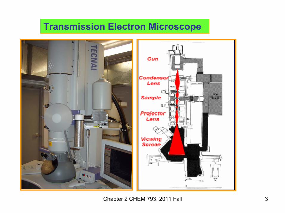
Transmission Electron Microscope

Chapter 2 CHEM 793, 2011 Fall 4
Electron Microscopy
Specimen
Scanning Electron Microscope (SEM) Dealing mainly with Surface
Electron Beam
Backscattered Secondary Electron to Image Specimen Topography
Transmission Electron Microscope (TEM) Dealing mainly with Internal Structure
Transmitted and Diffracted Electron to Image Specimen Internal Structure
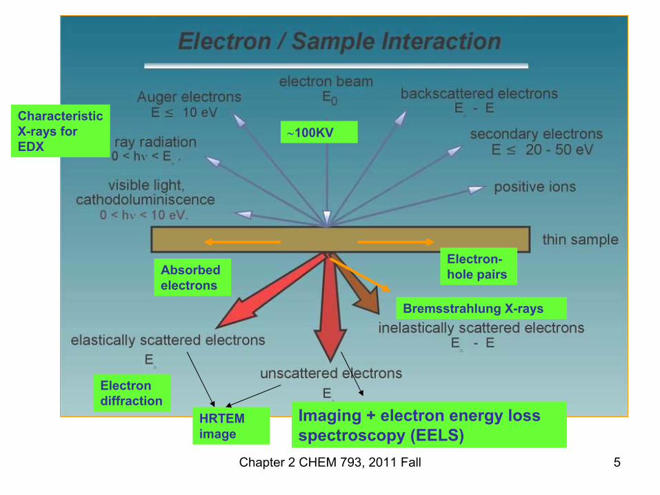
Chapter 2 CHEM 793, 2011 Fall 5
∼100KV
Electron diffraction
Absorbed electrons
Electron-hole pairs
Bremsstrahlung X-rays
Characteristic X-rays for EDX
HRTEM image
Imaging + electron energy loss spectroscopy (EELS)

Chapter 2 CHEM 793, 2011 Fall 6
Electron-specimen Scattering
• Electron scattering: without interactions we observe nothing
• Interaction cross-section: the probability of an event occurring (unit: barns)
• Elastic scattering: diffraction
• Inelastic scattering:
1. x-ray emission: characteristic, Bremstrahlung
2.Secondary electrons
3. Auger electrons
4. Plasmons
5. Phonons
• Beam damage: radiolysis and knock-on damage

Chapter 2 CHEM 793, 2011 Fall 7
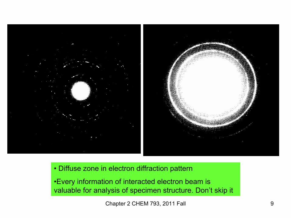
• Diffuse zone in electron diffraction pattern
•Every information of interacted electron beam is valuable for analysis of specimen structure. Don’t skip it
Chapter 2 CHEM 793, 2011 Fall 8
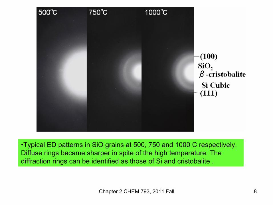
•Typical ED patterns in SiO grains at 500, 750 and 1000 C respectively. Diffuse rings became sharper in spite of the high temperature. The diffraction rings can be identified as those of Si and cristobalite .
Chapter 2 CHEM 793, 2011 Fall 9
• Diffuse zone in electron diffraction pattern
•Every information of interacted electron beam is valuable for analysis of specimen structure. Don’t skip it
Chapter 2 CHEM 793, 2011 Fall 10
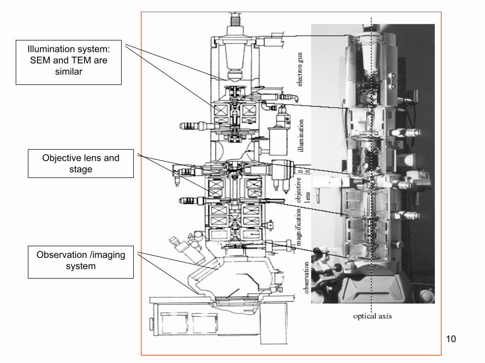
Illumination system: SEM and TEM are
similar
Objective lens and stage
Observation /imaging system

Chapter 2 CHEM 793, 2011 Fall 11
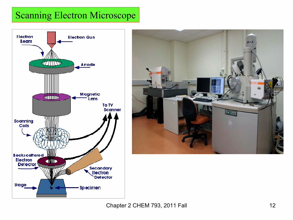
Chapter 2 CHEM 793, 2011 Fall 12
Scanning Electron Microscope

Chapter 2 CHEM 793, 2011 Fall 13

Chapter 2 CHEM 793, 2011 Fall 14
Family of Electron Microscopes
Scan Coils
Analytical STEM
STEMEPMASEMTEMAEM Analytical TEM/STEM
Microscope
CCD Camera
EELS
Screen Counter
Objective /projective lens
Specimen
Detectors
Condenser Lens
Gun
X E X E X E X E
Chapter 2 CHEM 793, 2011 Fall 15
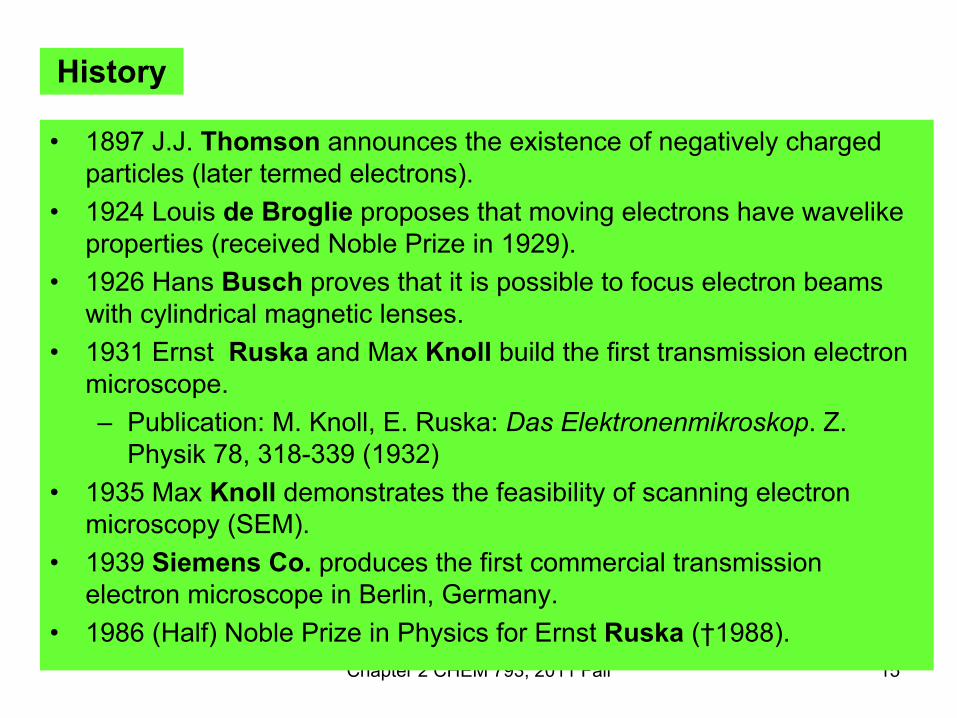
History
• 1897 J.J. Thomson announces the existence of negatively charged particles (later termed electrons).
• 1924 Louis de Broglie proposes that moving electrons have wavelike properties (received Noble Prize in 1929).
• 1926 Hans Busch proves that it is possible to focus electron beams with cylindrical magnetic lenses.
• 1931 Ernst Ruska and Max Knoll build the first transmission electron microscope. – Publication: M. Knoll, E. Ruska: Das Elektronenmikroskop. Z.
Physik 78, 318-339 (1932) • 1935 Max Knoll demonstrates the feasibility of scanning electron
microscopy (SEM).• 1939 Siemens Co. produces the first commercial transmission
electron microscope in Berlin, Germany. • 1986 (Half) Noble Prize in Physics for Ernst Ruska (†1988).
Chapter 2 CHEM 793, 2011 Fall 16
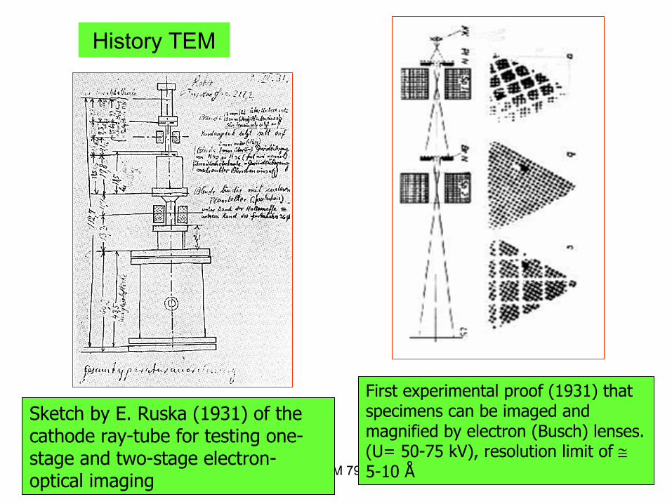
History TEM
Sketch by E. Ruska (1931) of the cathode ray-tube for testing one-stage and two-stage electron-optical imaging
First experimental proof (1931) that specimens can be imaged and magnified by electron (Busch) lenses. (U= 50-75 kV), resolution limit of ≅5-10 Å
Chapter 2 CHEM 793, 2011 Fall 17
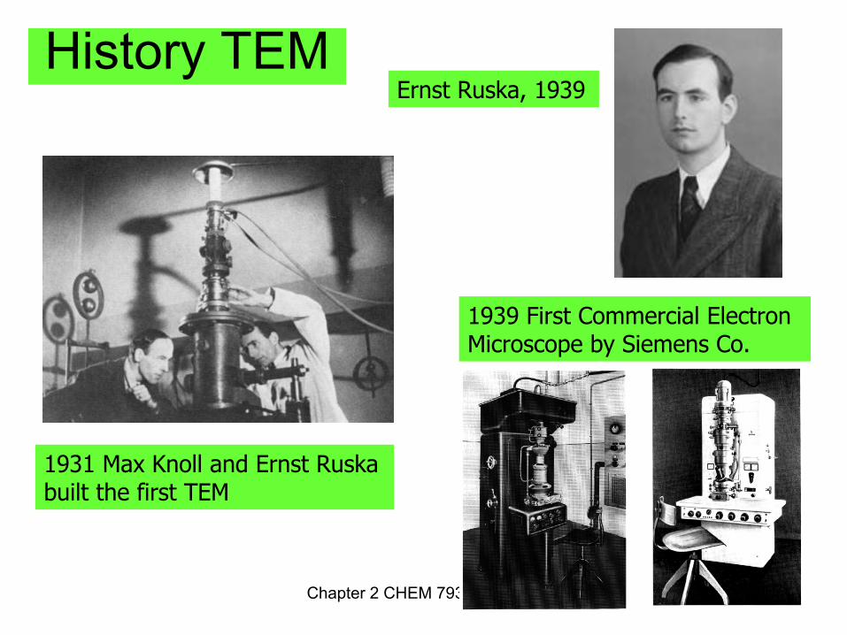
History TEMErnst Ruska, 1939
1931 Max Knoll and Ernst Ruskabuilt the first TEM
1939 First Commercial Electron Microscope by Siemens Co.
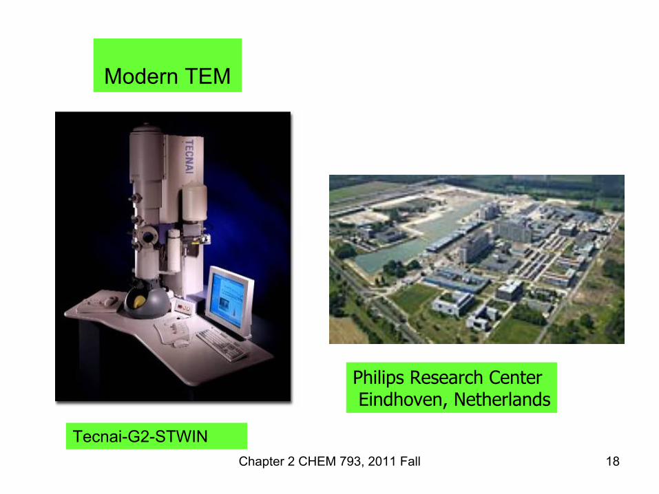
Chapter 2 CHEM 793, 2011 Fall 18
Modern TEM
Philips Research CenterEindhoven, Netherlands
Tecnai-G2-STWIN

Chapter 2 CHEM 793, 2011 Fall 19
The newest Cs-Corrected Transmission Electron Microscope
Model: FEI Titan 80-300Purpose: HRTEM, STEM, EELS, Energy Filtered TEM, Tomography, Electron Holography, LorentzmicroscopyDescription: up to 300kV accelerating voltage, HRTEM point-to-point resolution 0.08nm with Cs-corrector of objective lens, 0.13nmSTEM resolutionAdditions: Cs-corrector, Lorentz-lens system & Bi-prism (Holography), Gatan Tridiem(EELS), Tomography holder

Chapter 2 CHEM 793, 2011 Fall 20
Illumination system: SEM and TEM are
similar
Objective lens and stage
Observation/ imaging system
Chapter 2 CHEM 793, 2011 Fall 21
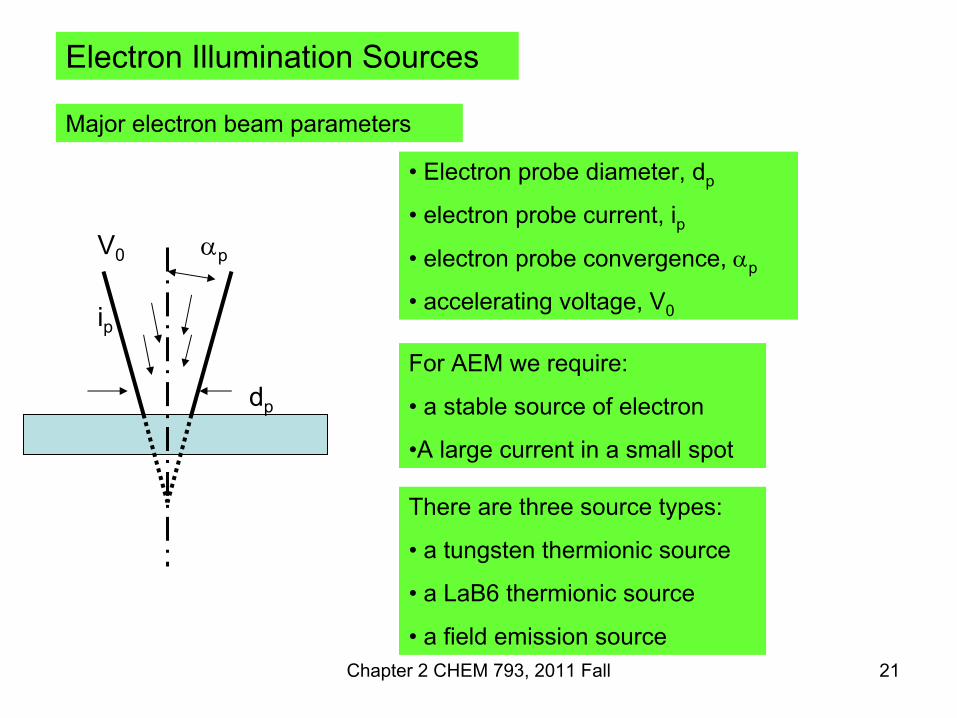
Electron Illumination Sources
Major electron beam parameters
• Electron probe diameter, dp
• electron probe current, ip• electron probe convergence, αp
• accelerating voltage, V0
For AEM we require:
• a stable source of electron
•A large current in a small spot
There are three source types:
• a tungsten thermionic source
• a LaB6 thermionic source
• a field emission source
dp
ip
αpV0
Chapter 2 CHEM 793, 2011 Fall 22
A. Thermionic Emission
Electron escapes from metal when it acquires enough thermal energy to overcome the work function (Φ) barrier
Richardson’s law
kTeATjΦ
−= 2
0
J0: Current density
T: operating temperature
K: Boltzmann’s constant, 8.5x10⁻⁵
eV/K
A: Richardson’s constant
Tungsten and LaB6 are used electron sources
A/cm2
Electron Illumination Sources
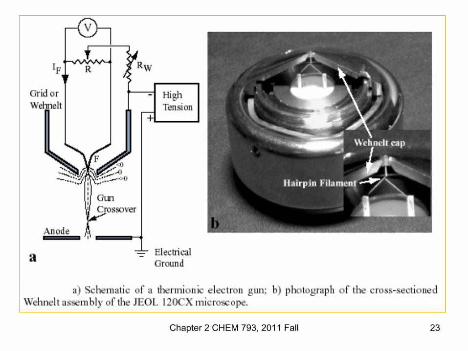
Chapter 2 CHEM 793, 2011 Fall 23

Chapter 2 CHEM 793, 2011 Fall 24
B. Field Emission Gun (FEG)
E: Electrical field strength
V: voltage
r: radius of tungsten tip
E=V/r
Electron Illumination Sources
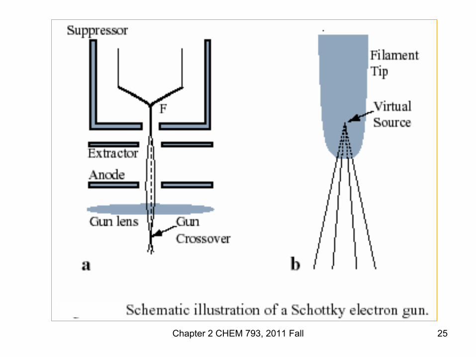
Chapter 2 CHEM 793, 2011 Fall 25
Chapter 2 CHEM 793, 2011 Fall 26
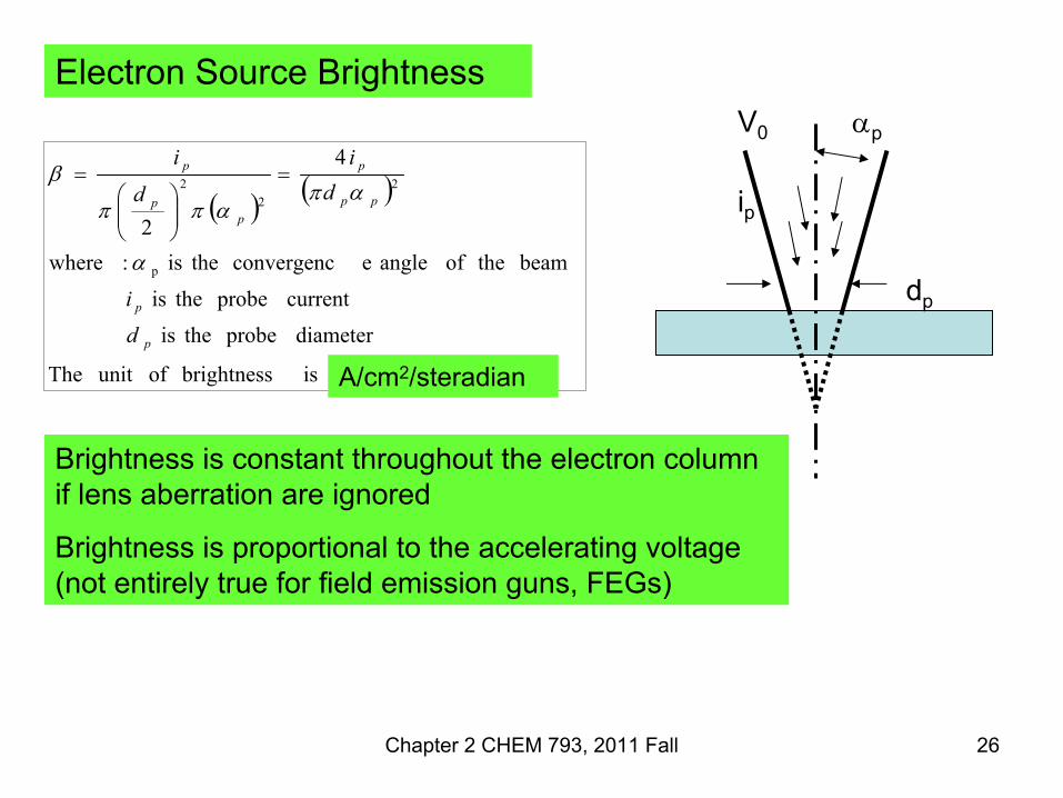
Electron Source Brightness
( ) ( )
steradian/A/cm is brightness ofunit The
diameter probe theis
current probe theis
beam theof angle econvergenc theis :where
4
2
2
p
22
2
p
p
pp
p
pp
p
d
i
di
d
i
α
απαππ
β =
=
Brightness is constant throughout the electron column if lens aberration are ignored
Brightness is proportional to the accelerating voltage (not entirely true for field emission guns, FEGs)
dp
ip
αpV0
A/cm2/steradian
Chapter 2 CHEM 793, 2011 Fall 27
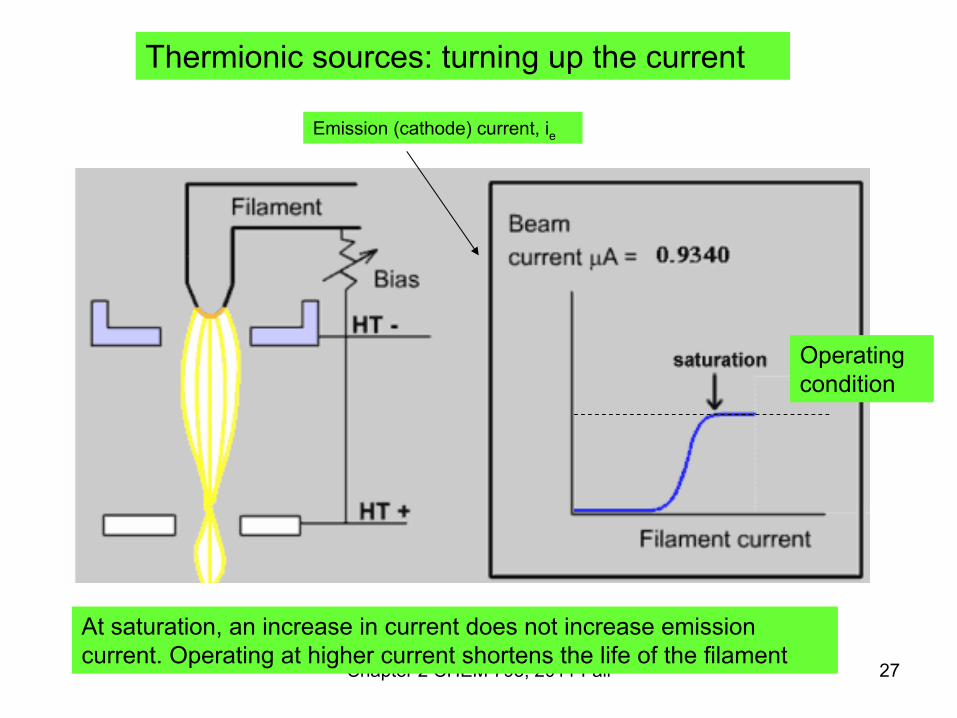
Thermionic sources: turning up the current
Emission (cathode) current, ie
Operating condition
At saturation, an increase in current does not increase emissioncurrent. Operating at higher current shortens the life of the filament
Chapter 2 CHEM 793, 2011 Fall 28
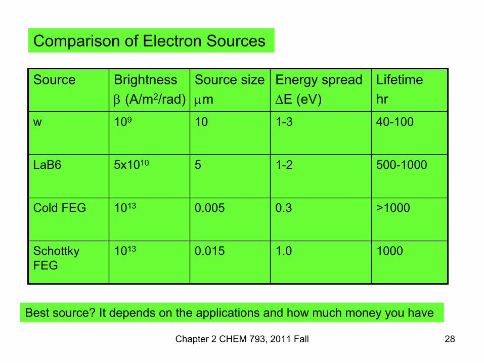
Comparison of Electron Sources
1.0
0.3
1-2
1-3
Energy spread∆E (eV)
10000.0151013SchottkyFEG
>10000.0051013Cold FEG
500-100055x1010LaB6
40-10010109w
Lifetimehr
Source sizeµm
Brightnessβ (A/m2/rad)
Source
Best source? It depends on the applications and how much money you have

Chapter 2 CHEM 793, 2011 Fall 29
Calculating the beam diameter (or called probe size in convergent beam)
• The beam diameter is defined as the full width at half maximum (FWHM) of the Gaussian distribution.
• The actual beam diameter results from:(a). the diameter of the original beam leaving the electron gun, dg,(b). broadened by the effect of spherical and chromatic aberration in the lenses ds, dc, (c). diffraction at the aperture, dd.
All effects depend on the current density, jc, convergence angle (αp), brightness, β , spherical/chromatic aberration coefficient Cs/Cc, and wavelength, λ.
I max
I max /2 FWHM
I max /10
The intensity of a well aligned beam is a Gaussian distribution
Chapter 2 CHEM 793, 2011 Fall 30
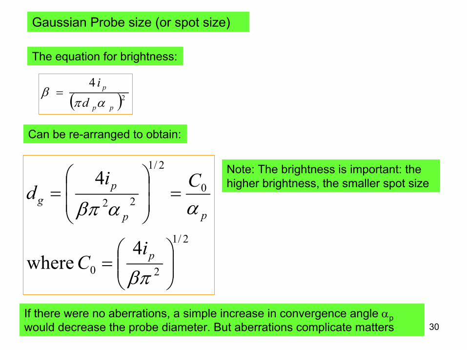
Gaussian Probe size (or spot size)
( )24
pp
p
diαπ
β =
2/1
20
0
2/1
22
4 where
4
=
=
=
βπ
ααβπ
p
pp
pg
iC
Cid
Note: The brightness is important: the higher brightness, the smaller spot size
If there were no aberrations, a simple increase in convergence angle αpwould decrease the probe diameter. But aberrations complicate matters
The equation for brightness:
Can be re-arranged to obtain:

Chapter 2 CHEM 793, 2011 Fall 31
Spherical aberration, Cs
Disc of least confusion, ds
Focus for marginal rays is nearer to lens than the focus for paraxial rays
Axial focus
35.0 pss Cd α= ds: beam broadened by sphere aberration
Cs: sphere aberration coefficient
Chapter 2 CHEM 793, 2011 Fall 32
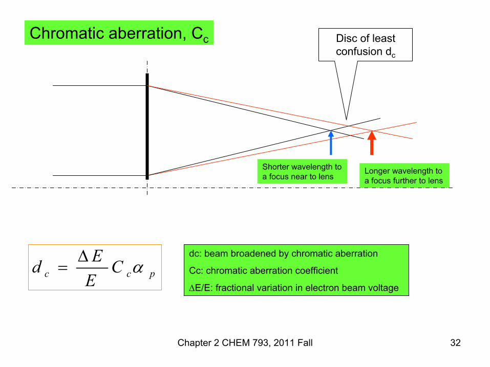
Disc of least confusion dc
Shorter wavelength to a focus near to lens
Longer wavelength to a focus further to lens
Chromatic aberration, Cc
pcc CEEd α∆
=dc: beam broadened by chromatic aberration
Cc: chromatic aberration coefficient
∆E/E: fractional variation in electron beam voltage
Chapter 2 CHEM 793, 2011 Fall 33
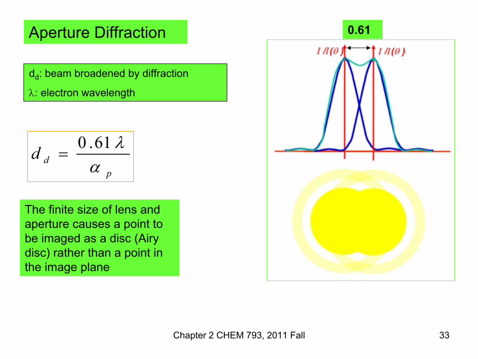
pdd α
λ61.0=
dd: beam broadened by diffraction
λ: electron wavelength
Aperture Diffraction 0.61
The finite size of lens and aperture causes a point to be imaged as a disc (Airy disc) rather than a point in the image plane

Chapter 2 CHEM 793, 2011 Fall 34
dd
Airy disc

Chapter 2 CHEM 793, 2011 Fall 35
Astigmatism Magnetic in-homogeneities in the lens materialsMachining errorsDirty apertures or lensesAstigmatism is fully correctable using an octupole stigmatorSo ignore astigmatism in calculating probe size
Disc of least confusion
Vertical focal line Horizontal focal line
y
x
Chapter 2 CHEM 793, 2011 Fall 36
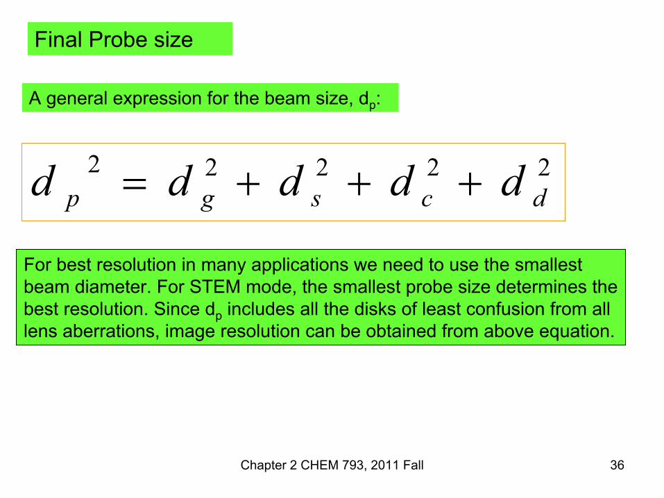
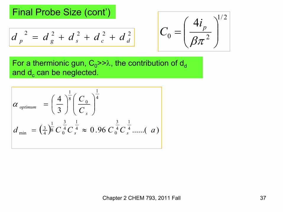
Final Probe size
22222dcsgp ddddd +++=
A general expression for the beam size, dp:
For best resolution in many applications we need to use the smallest beam diameter. For STEM mode, the smallest probe size determines the best resolution. Since dp includes all the disks of least confusion from all lens aberrations, image resolution can be obtained from above equation.
Chapter 2 CHEM 793, 2011 Fall 37
Final Probe Size (cont’)
22222dcsgp ddddd +++=
( ) )......(96.0
34
41
43
041
43
081
43
min
41
081
aCCCCd
CC
ss
soptimum
≈=
=α
For a thermionic gun, C0>>λ, the contribution of ddand dc can be neglected.
2/1
20
4
=
βπpiC

Chapter 2 CHEM 793, 2011 Fall 38
Final Probe Size (cont’)
22222dcsgp ddddd +++=
(b) ..... 8.0
9.0
41
43
min
41
s
soptimum
Cd
C
λ
λα
=
=
For a FEG gun, C0<<λ, the contribution of dg and dc can be neglected.
2/1
20
4
=
βπpiC
These expressions can be used to estimate the optimum aperture angle and the resolution limit of a high resolution TEM/STEM . Equation (b) is especially important for evaluating the capabilities of different TEM instruments.
Note that for resolution depends more strongly λ than Cs. This encourages the use of high accelerating voltage (small λ). Cs can be corrected by current technology.

Chapter 2 CHEM 793, 2011 Fall 39
Probe size @ V0=200 KV and λ=2.5 pm
FEG LaB6
dd
dg
ds
Wαp

Chapter 2 CHEM 793, 2011 Fall 40
Summary of Probe Formation
• Small electron probe generation is limited by
1. spherical aberration
2. Chromatic aberration
3. diffraction error
• Careful choice of convergence angle (final aperture size) is critical to forming the smallest probe with highest current
• Too large an aperture will result in spherical aberration
•Too small an aperture results in low probe current and a larger aberratedprobe due to diffraction effects
Chapter 2 CHEM 793, 2011 Fall 41
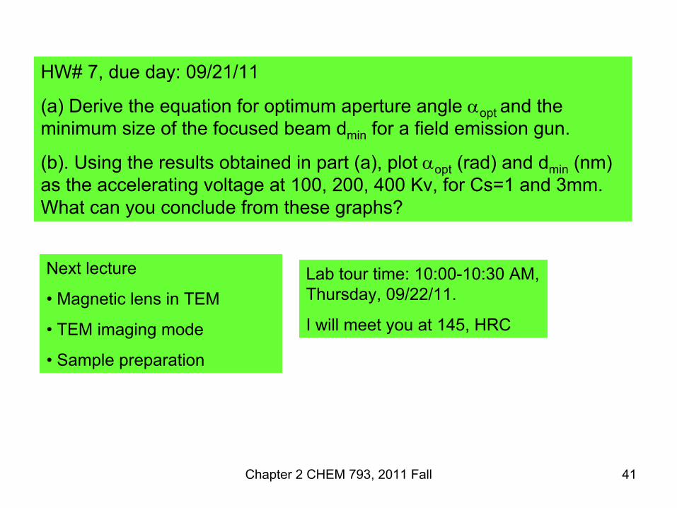
HW# 7, due day: 09/21/11
(a) Derive the equation for optimum aperture angle αopt and the minimum size of the focused beam dmin for a field emission gun.
(b). Using the results obtained in part (a), plot αopt (rad) and dmin (nm) as the accelerating voltage at 100, 200, 400 Kv, for Cs=1 and 3mm. What can you conclude from these graphs?
Next lecture
• Magnetic lens in TEM
• TEM imaging mode
• Sample preparation
Lab tour time: 10:00-10:30 AM, Thursday, 09/22/11.
I will meet you at 145, HRC