M. G. D. Gilchriese (LBNL) Interim Deputy Project Director ...
Upload
ethan-crossCategory
view
216download
0
M. Gilchriese -February 1999
X-Ray Inspection of Flip Chip Assemblies
K. Einsweiler, M. Gilchriese and J. Richardson
LBNL

M. Gilchriese -February 19992
X-Ray Source
• X-Ray inspection from X-Tek– Model VTX
• 2 micron resolution• 1800 X magnification• Large area, precision x-y table, with rotation
– www.xtek.co.uk– Inspection services offered
• Local office near LBL• Allow us to use equipment after short training to do
inspection. • They will also do inspection
– Very easy to use
M. Gilchriese -February 19993
Seiko Solder Bump Dummy 16-Chip Module
M. Gilchriese -February 19994
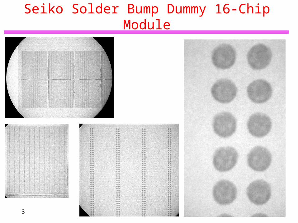
Boeing Indium Bump Dummy 16-Chip Module
Region of poor registration Nearly merged Merged bumps
Older design with single column

M. Gilchriese -February 19995
Active Devices
• Bare die(indium bumps)
• Unmounted single-chip assembly(both solder and indium)
• Single-chip assemblies on PC boards
• Full 16 chip module on PC board and aluminum plate

M. Gilchriese -February 19996
Bare Die and Single-Chip Assembly(Indium Bumps)
Bare indium diebefore flip-chip assembly
50
Single-chipassembly withindium(SCP)
Same as above buthigher magnification

M. Gilchriese -February 19997
Single-Chip Assembly(IZM Solder Bumps)
Region with missing bump
Higher magnification - notice voids
M. Gilchriese -February 19998
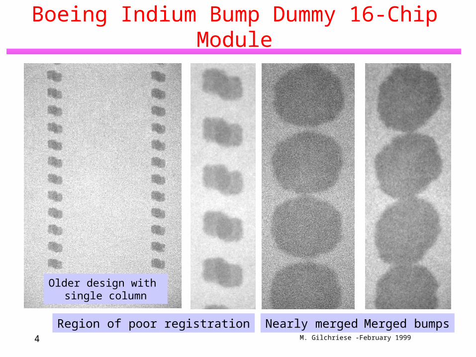
Active Devices - SSG(Solder Bumps)
Column 0
Title:cis_ssg_nds_cd109.epsCreator:HIGZ Version 1.23/07Preview:This EPS picture was not savedwith a preview included in it.Comment:This EPS picture will print to aPostScript printer, but not toother types of printers.
Column 0and 1-2 Complete correlation between pairs of dead
and double rate channels with bridged bumps
Column 1-2

M. Gilchriese -February 19999
Active Devices - S80(Indium Bumps)
Column 0Rows near 0
Merged bumps
Columns 1-2Rows near 0
Title:cis_s8o_nds_cd109.epsCreator:HIGZ Version 1.23/07Preview:This EPS picture was not savedwith a preview included in it.Comment:This EPS picture will print to aPostScript printer, but not toother types of printers.
Unattached
region
M. Gilchriese -February 199910
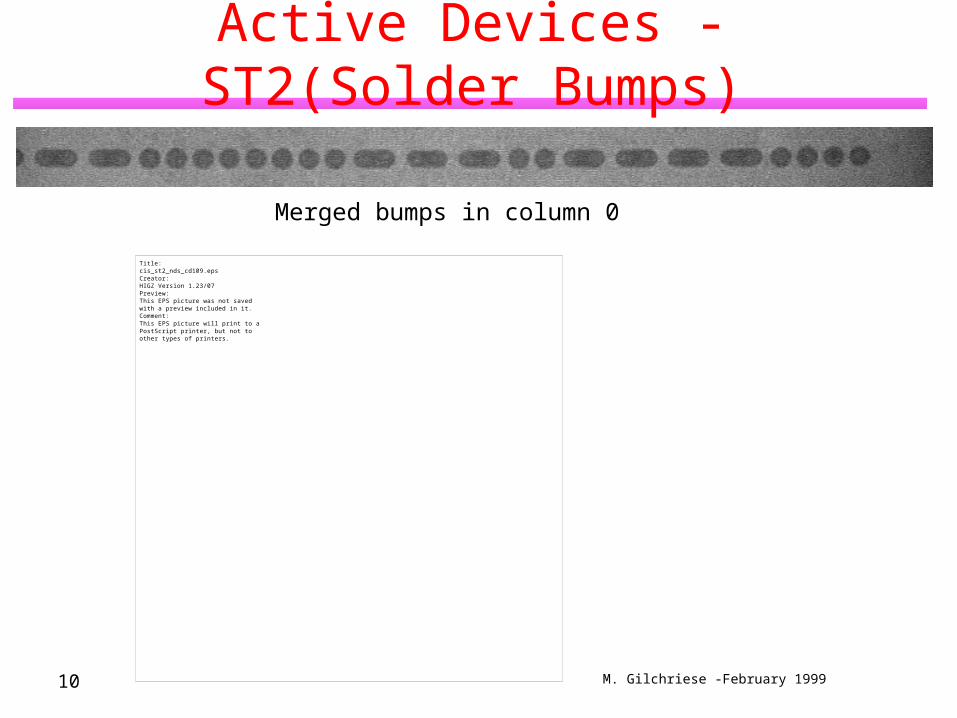
Active Devices - ST2(Solder Bumps)
Merged bumps in column 0
Title:cis_st2_nds_cd109.epsCreator:HIGZ Version 1.23/07Preview:This EPS picture was not savedwith a preview included in it.Comment:This EPS picture will print to aPostScript printer, but not toother types of printers.

M. Gilchriese -February 199911
Module(Indium Bumps)
Chip 15good region
Chip 4 column 3-4 bad region
Chip 4 column 3-4 good region
• Resolution not as good with module on top of aluminum plate
• But still clear correlation between dead channels and regions of merged/bridged bumps
• Simple mechanical modifications to support would be needed to improve resolution - mill out hole in plate.

M. Gilchriese -February 199912
Diamond Devices
CDS62columns 7- 8
Merged bumps
CDS62columns 3-4
• Two diamond assemblies - CDS61 and CDS62
• Both show same feature of region of merged bumps near center of die.
• Diamond not flat - local region. Need to measure flatness before bumping.
• There was some indication of this already from person doing original lithography for photoresist.
• However, this does not readily explain why most(almost all) of channels are not responding. Most of bumps look OK away from center.
M. Gilchriese -February 199913
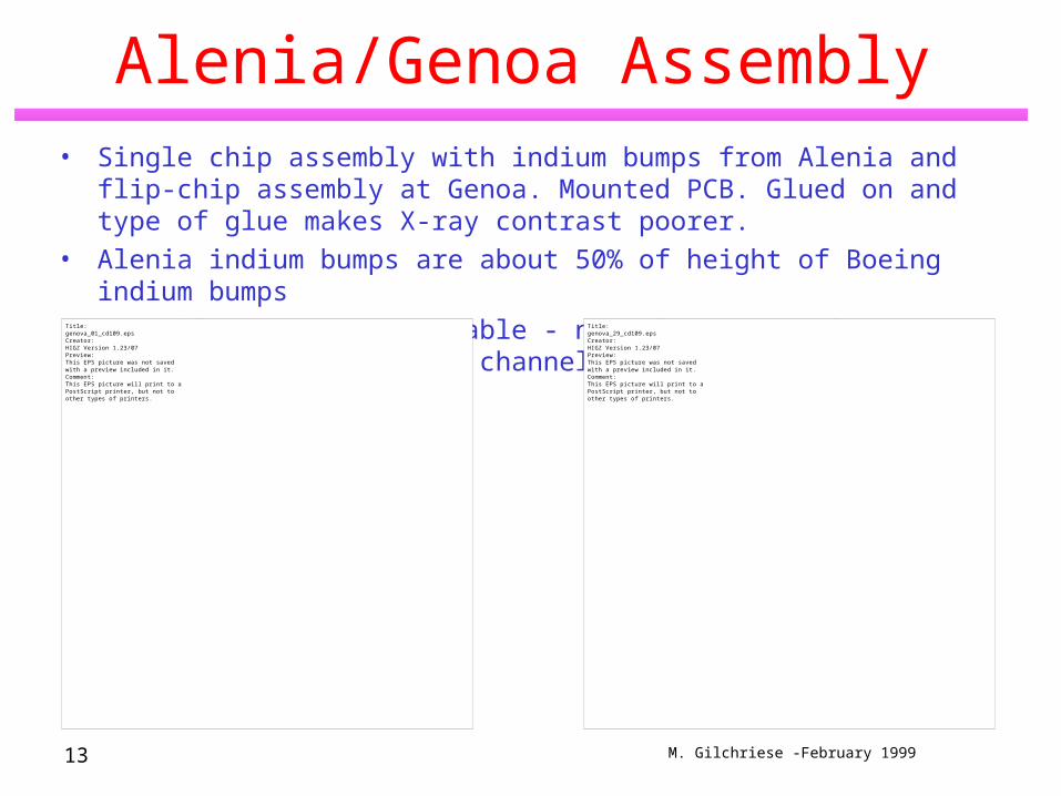
Alenia/Genoa Assembly• Single chip assembly with indium bumps from Alenia and flip-chip assembly at
Genoa. Mounted PCB. Glued on and type of glue makes X-ray contrast poorer.
• Alenia indium bumps are about 50% of height of Boeing indium bumps
• Assembly is noisy, unstable - not clear why. Also seems to have regions of dead channels. Hard to do all of chip with source.
Title:genova_01_cd109.epsCreator:HIGZ Version 1.23/07Preview:This EPS picture was not savedwith a preview included in it.Comment:This EPS picture will print to aPostScript printer, but not toother types of printers.
Title:genova_29_cd109.epsCreator:HIGZ Version 1.23/07Preview:This EPS picture was not savedwith a preview included in it.Comment:This EPS picture will print to aPostScript printer, but not toother types of printers.

M. Gilchriese -February 199914
Alenia/Genoa Assembly• Noise measurements. Correlation? Lower noise for unconnected channels.. Maybe.
Title:genova_noise_log.epsCreator:HIGZ Version 1.23/07Preview:This EPS picture was not savedwith a preview included in it.Comment:This EPS picture will print to aPostScript printer, but not toother types of printers.
Title:genova_2880.epsCreator:HIGZ Version 1.23/07Preview:This EPS picture was not savedwith a preview included in it.Comment:This EPS picture will print to aPostScript printer, but not toother types of printers.
M. Gilchriese -February 199915
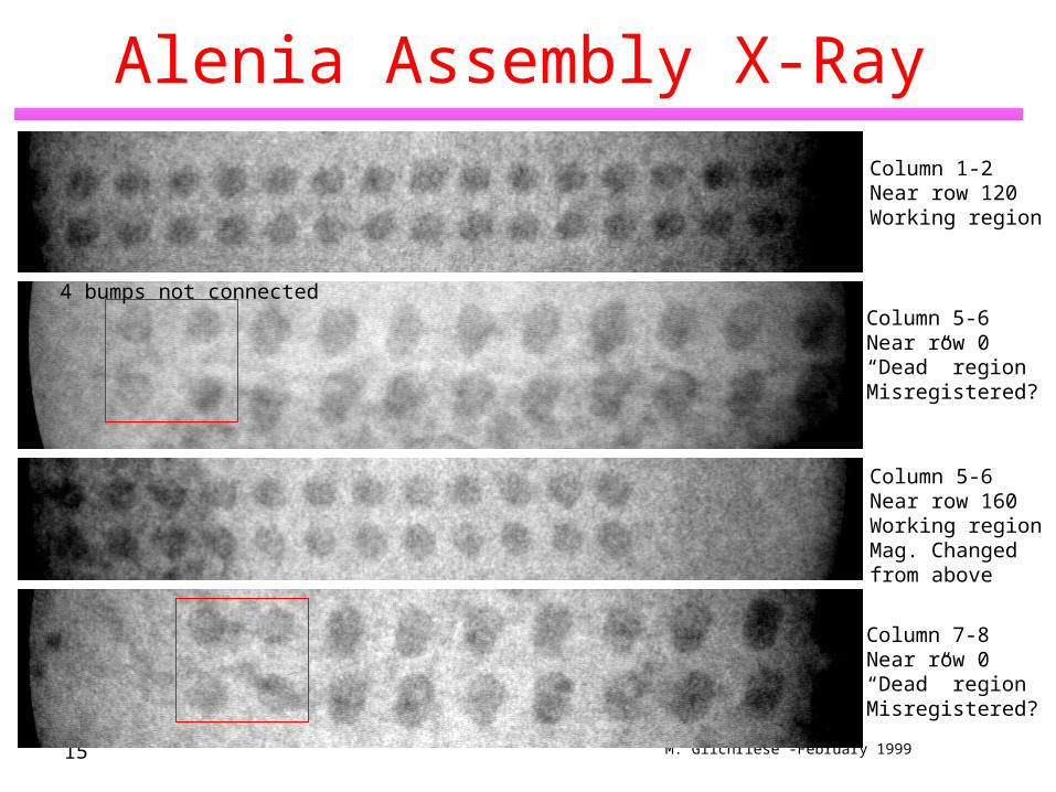
Alenia Assembly X-Ray
Column 1-2Near row 120Working region
4 bumps not connectedColumn 5-6Near row 0“Dead” regionMisregistered?
Column 5-6Near row 160Working regionMag. Changed from above
.
Column 7-8Near row 0“Dead” regionMisregistered?
M. Gilchriese -February 199916
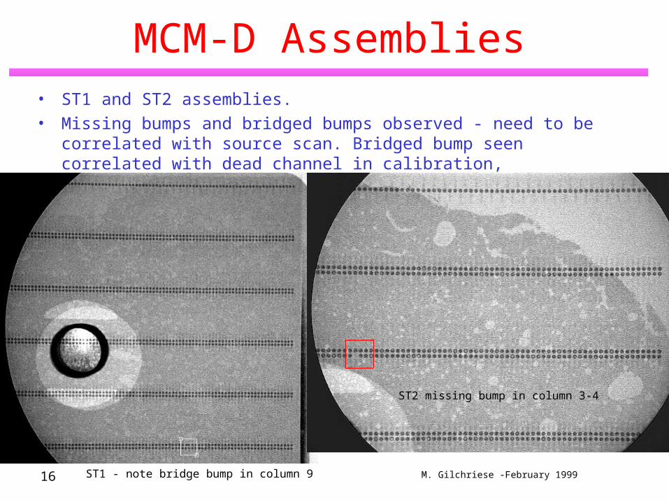
MCM-D Assemblies• ST1 and ST2 assemblies.
• Missing bumps and bridged bumps observed - need to be correlated with source scan. Bridged bump seen correlated with dead channel in calibration,
ST1 - note bridge bump in column 9
ST2 missing bump in column 3-4

M. Gilchriese -February 199917
MCM-D Source Maps
Title:mcmd1cd109.epsCreator:HIGZ Version 1.23/07Preview:This EPS picture was not savedwith a preview included in it.Comment:This EPS picture will print to aPostScript printer, but not toother types of printers.
Title:mcmd2cd109.epsCreator:HIGZ Version 1.23/07Preview:This EPS picture was not savedwith a preview included in it.Comment:This EPS picture will print to aPostScript printer, but not toother types of printers.

M. Gilchriese -February 199918
Flex Module• Boeing indium bumps. Mostly see dead regions
correlated with merged bumps. Still need to do more correlation with source scan.
Chip 13. Region of many dead channels.Likely merged bumps.
Chip 13. Same column as at left but in region of live channels

M. Gilchriese -February 199919
IZM Bare Modules• Looked at module broken during shipment and undamaged module. Both are bare.• Scanned for bridges and missing. May miss some bridges(see 1st picture). Able to
scan with module in gelpak.• Assuming defects =2*bridged+missing, rate is 1-2%.
DieBridged Missing Bridged Missing
0 7 1 15 01 0 1 20 02 0 1 3 03 10 0 6 04 26 0 8 15 2 0 52 06 2 0 23 07 2 0 3 08 46 0 27 09 5 0 3 0
10 24 1 16 011 44 0 31 012 106 0 3 013 35 0 10 014 43 0 3 015 ------ ------ 42 2
Total 352 4 265 3Defects% defects
Broken Good
7081.6%
5331.2%

M. Gilchriese -February 199920
Conclusions• Boeing indium flip chip assembly shows “slippage”. Possibly
similar evidence for Alenia/Genoa but much more statistics needed.
• Solder flip-chip(at single assembly level) appears better but first look at modules shows defect rate 1-2%, a bit high.
• Demonstrated diagnostic tool for evaluation of flip chip assembly problems
• Simple mechanical modifications would allow higher resolution• Can this be used to scan bare modules in production?
– Yes– Can easily program automated step/stop/look sequence(but look only by
eye)– Need real estimate, but guess would be 15-30 min per module with proper
setup and experience.– The average module production rate is supposed to be about 30 per week =>
roughly two days per week of inspection to keep up.• X-TEK is UK company. Capability also exists in Europe.• There are other potential vendors to explore.