
LTV-50L series Product Data Sheet Photocoupler...2 /1 2 Photocoupler L TV -5 0L series P art No. :...
13
LITE-ON DCC RELEASE LITE-ON Technology Corp. / Optoelectronics No.90,Chien 1 Road, Chung Ho, New Taipei City 23585, Taiwan, R.O.C. Tel: 886-2-2222-6181 Fax: 886-2-2221-1948 / 886-2-2221-0660 http://www.liteon.com/opto Photocoupler Product Data Sheet LTV-50L series Spec No.: DS70-2015-0058 Effective Date: 03/22/2016 Revision: B BNS-OD-FC001/A4
Transcript of LTV-50L series Product Data Sheet Photocoupler...2 /1 2 Photocoupler L TV -5 0L series P art No. :...
LITE-ON DCC
RELEASE
LITE-ON Technology Corp. / OptoelectronicsNo.90,Chien 1 Road, Chung Ho, New Taipei City 23585, Taiwan, R.O.C.
Tel: 886-2-2222-6181 Fax: 886-2-2221-1948 / 886-2-2221-0660http://www.liteon.com/opto
PhotocouplerProduct Data SheetLTV-50L series Spec No.: DS70-2015-0058Effective Date: 03/22/2016
Revision: B
BNS-OD-FC001/A4
BNS-OD-FC001/A4
BNS-OD-FC001/A4
BNS-OD-FC001/A4

1/12
Photocoupler
LTV-50L series
Part No. : LTV-50L series
BNC-OD-FC002/A4
1. DESCRIPTION
The LTV-50L series consists of a high efficient AlGaAs Light Emitting Diode and a high speed optical detector. This design provides
excellent AC and DC isolation between the input and output sides of the Optocoupler. The output of the optical detector features an
open collector Schottky clamped transistor. The internal shield ensures high common mode transient immunity. A guaranteed
common mode transient immunity is up to 15KV/μs (min.). The Optocoupler operational parameters are guaranteed over the
temperature range from -55°C ~ +100°C.
1.1 Features
Stretched SO6
High speed – 1MBd typical
Package creepage at 8mm
Compatible with infrared vapor phase reflow and wave soldering process
Very high common mode transient immunity: 15K V/μs at VCM = 1500 V guaranteed
Guarantee performance from temperature range: -55°C to 100°C
TTL compatible
Open collector output
Safety approval :
UL 1577 recognized with 5000 Vrms for 1 minute for
LTV-50LP and LTV-50LW
VDE DIN EN 60747-5-5 Approved
VIORM = 891Vpeak for LTV-50LP
VIORM = 1140Vpeak for LTV-50LW
1.2 Applications
Digital signal isolation
Communications interface
Micro-controller interface
Feedback elements in switching power supplies
Digital isolation for A/D, D/A conversion Digital field
Functional Diagram
Pin No. and Internalconnection diagram
3. Cathode
1. Anode
1 3
6 5 4
4. GND
5. Vo (Output)
6. Vcc
2
A 0.1μF bypass Capacitor must be connected
between Pin 4 and 6. *1
A 0.1μF bypass Capacitor must be connected
between Pin 5 and 8. See note 11.
Truth Table (Positive Logic)
LED OUT
ON LOW
OFF HIGH

2/12
Photocoupler
LTV-50L series
Part No. : LTV-50L series
BNC-OD-FC002/A4
2. PACKAGE DIMENSIONS
2.1 LTV-50LW 2.2 LTV-50LP
Notes :
1. Year date code.
2. 2-digit work week.
3. Factory identification mark (Y : Thailand).
4. ―4‖ or ‖V‖ for VDE option.
* Dimensions are in Millimeters and (Inches).

3/12
Photocoupler
LTV-50L series
Part No. : LTV-50L series
BNC-OD-FC002/A4
3. TAPING DIMENSIONS
3.1 LTV-50LW-TA 3.2 LTV-50LW-TA1
3.3 LTV-50LP-TA 3.4 LTV-50LP-TA1
3.5 Quantities Per Reel
Description Symbol Dimension in mm (inch)
For W type
Dimension in mm (inch)
For P type
Tape wide W 16±0.3 (0.63) 16±0.3 (0.63)
Pitch of sprocket holes P0 4±0.1 (0.16) 4±0.1 (0.16)
Distance of compartment F 7.5±0.1 (0.3) 7.5±0.1 (0.3)
P2 2±0.1 (0.079) 2±0.1 (0.079)
Distance of compartment to compartment P1 16±0.1 (0.63) 12±0.1 (0.47)
Package Type LTV-50L series
Quantities (pcs) 1000

4/12
Photocoupler
LTV-50L series
Part No. : LTV-50L series
BNC-OD-FC002/A4
4. RATING AND CHARACTERISTICS
4.1 Absolute Maximum Ratings
Parameter Symbol Min Max Units Note
Storage Temperature TST -55 125 °C —
Operating Temperature TA -55 100 °C —
Isolation Voltage VISO 5000 — VRMS —
Supply Voltage VCC -0.5 30 V —
Lead Solder Temperature — — 260 °C 2
Input
Average Forward Input Current IF — 25 mA —
Peak Input Current
(50% duty cycle, 1 ms pulse width) IF — 50 mA 3
Peak Transient Input Current
(1 μs pulse width, 300 pps) IF — 1.0 A —
Reverse Input Voltage VR — 5 V —
Input Power Dissipation PI — 45 mW —
Output
Output Collector Current IO — 8 mA —
Peak Output Current IO — 16 mA —
Output Collector Voltage VO -0.5 20 V —
Output Collector Power Dissipation PO — 100 mW —
*Ambient temperature = 25°C, unless otherwise specified. Stresses exceeding the absolute maximum ratings can
cause permanent damage to the device. Exposure to absolute maximum ratings for long periods of time can
adversely affect reliability.

5/12
Photocoupler
LTV-50L series
Part No. : LTV-50L series
BNC-OD-FC002/A4
4.2 Electrical Optical Characteristics
Parameters Test Condition Symbol Min Typ Max Units Note
Input
Input Forward Voltage IF =16mA, TA=25 °C VF 1.2 1.4 1.8 V —
Input Reverse Voltage IR = 10μA BVR 5 — — V —
Detector
* Current transfer ratio
IF = 16mA; VCC = 4.5V;
TA = 25 °C; VO = 0.4V CTR
20 32 —
% — IF = 16mA; VCC = 4.5V;
TA = 25°C; VO = 0.5V 15 33 —
Logic low output voltage
output voltage
IF = 16mA;VCC = 4.5V;
Io = 3.0mA; TA = 25°C VOL
— 0.2 0.4
V — IF = 16mA;VCC = 4.5V;
Io = 2.4mA; TA = 25°C — — 0.5
Logic high output current
IF = 0mA, VO = VCC = 5.5V,
TA = 25°C
IOH
— 0.002 0.5
μA
— IF = 0mA, VO = VCC = 15V
TA = 25°C — 0.005 1
TA = 0 ~ 70°C — — 50
Logic low supply current IF = 16mA, Vo = open
(VCC=30V) ICCL — 165 —
Logic high supply current IF = 0mA, Vo = open ;
TA = 25°C (VCC = 30V) ICCH — 0.002 1 —
*All Typical values at TA = 25°C unless otherwise specified. All minimum and maximum specifications are at recommended
operating condition.
*Current Transfer Ratio in percent is defined as the ratio of output collector current, IO, to the forward LED input current, IF,
times 100%.

6/12
Photocoupler
LTV-50L series
Part No. : LTV-50L series
BNC-OD-FC002/A4
5. SWITCHING SPECIFICATION
Parameter Test Condition Symbol Min Typ Max Units Note
Propagation Delay Time to
Low Output Level
TA = 25°C
RL=1.9KΩ
tPHL
— 190 800
ns
5
0 ~ 100°C — — 800
Propagation Delay Time to
High Output Level
TA = 25°C
tPLH
— 150 800
4
0 ~ 100°C — — 800
Logic High Common Mode
Transient Immunity
IF = 0mA;VCM = 1500Vp-p;
CL = 15 pF; TA=25°C ,
RL=1.9KΩ
|CMH| 15 25 — KV/μs 6
Logic Low Common Mode
Transient Immunity
IF = 16mA;VCM = 1500Vp-p
CL = 15 pF; TA = 25°C ,
RL = 1.9KΩ
|CML| 15 25 — KV/μs 7
*All Typical values at TA = 25°C unless otherwise specified. All minimum and maximum specifications are at recommended
operating condition.

7/12
Photocoupler
LTV-50L series
Part No. : LTV-50L series
BNC-OD-FC002/A4
6. ISOLATION CHARACTERISTIC
Parameter Test Condition Symbol Min Typ Max Units Note
Input-Output Insulation
Leakage Current
45% RH, t = 5s,
VI-O = 3kV DC, TA = 25°C II-O — — 1.0 μA 8
Withstand Insulation Test
Voltage
RH ≤ 50%, t = 1min,
TA = 25°C VISO 5000 — — Vrms 8,9
Input-Output Resistance VI-O = 500V DC RI-O — 1012 — Ω 8
*All Typical values at TA = 25°C unless otherwise specified. All minimum and maximum specifications are at recommended
operating condition.
NOTES:
1) A 0.1µF or bigger bypass capacitor for VCC is needed.
2) 260°C for 10 seconds
3) Peaking driving circuit may be used to speed up the LED. The peak drive current of LED may go up to 50mA and
maximum pulse width 50ns, as long as average current doesn’t exceed 20mA.
4) tPLH (propagation delay) is measured from the 3.75 mA point on the falling edge of the input pulse to the 1.5 V point on the
rising edge of the output pulse.
5) tPHL (propagation delay) is measured from the 3.75 mA point on the rising edge of the input pulse to the 1.5 V point on the
falling edge of the output pulse.
6) CMH is the maximum tolerable rate of rise of the common mode voltage to assure that the output will remain in a high
logic state
7) CML is the maximum tolerable rate of fall of the common mode voltage to assure that the output will remain in a low logic
state
8) Device is considered a two-terminal device: pins 1, 2, 3 shorted together, and pins 4, 5, 6 shorted together.
9) In accordance with UL1577, each optocoupler is proof tested by applying an insulation test voltage 6000 Vrms for one
second (leakage current less than 10 uA).

8/12
Photocoupler
LTV-50L series
Part No. : LTV-50L series
BNC-OD-FC002/A4
7. TYPICAL PERFORMANCE CURVES & TEST CIRCUITS
0
2
4
6
8
10
12
14
16
18
0 5 10 15 20
I O-
Outp
ut
Curr
ent
-m
A
VO - Output Voltage - V
TA = 25oC
VCC = 5V
IF = 5mA
10mA
15mA
20mA
25mA
30mA
35mA
40mA
0.001
0.01
0.1
1
10
100
0.9 1 1.1 1.2 1.3 1.4 1.5 1.6
I F-
Fo
rwar
d C
urr
ent
-m
A
VF - Forward Voltage - V
TA = 25oC
Figure 1: DC and Pulsed Transfer Characteristics Figure 2: Input Current vs. Forward Voltage
0
100
200
300
400
500
600
1 10
t P -
Pro
pag
atio
n D
elay
-n
s
RL - Load Resistance - kΩ
tPHL
tPLH
IF = 10mA
IF = 16mA
0
0.2
0.4
0.6
0.8
1
1.2
0.1 1 10 100
Norm
aliz
ed C
urr
ent
Tra
nsf
er R
atio
IF - Forward Current - mA
Normalized to
IF = 16mA
VO = 0.4V
VCC = 5V
TA = 25oC
Figure 3: Propagation Delay vs. Load Resistance. Figure 4: Current Transfer Ratio vs. Input Current.
0
0.2
0.4
0.6
0.8
1
1.2
-60 -40 -20 0 20 40 60 80 100
No
rmal
ized
Cu
rren
t T
ransf
er R
atio
TA - Ambient Temperature - oC
Normalized to
IF = 16mA
VO = 0.4V
VCC = 5V
TA = 25oC
0
100
200
300
400
500
-60 -40 -20 0 20 40 60 80 100
t P-
Pro
pag
atio
n D
elay
-n
s
TA - Ambient Temperature - oC
IF = 16mA, VCC = 5.0V
RL = 1.9KΩ
tPLH
tPHL
Figure 5: Current Transfer Ratio vs. Temperature. Figure 6: Propagation Delay Time vs. Temperature.

9/12
Photocoupler
LTV-50L series
Part No. : LTV-50L series
BNC-OD-FC002/A4
1
10
100
-60 -20 20 60 100
TA - Temperature - oC
I OH -
Lo
gic
Hig
h O
utp
ut
Cu
rren
t -
nA
IF = 0
VO = VCC = 5.0V
-25
-20
-15
-10
-5
0
5
0.01 0.1 1 10
f - Frequency - MHzN
orm
aliz
ed R
esp
on
se -
dB
RL = 100Ω
RL = 220Ω
RL = 470Ω
RL = 1KΩ
TA = 25oC
IF = 16mA
VCC = 5.0V
Figure 7: Logic High Output Current vs. Temperature. Figure 8: Frequency Response
1
3
6
5
4
CL
RM
I F MONITOR
PULSEGEN.
ZO = 50Ω t r = 5 ns
10% DUTY CYCLE1/f < 500us
I F
RL
VO
0.1 uF
HLtp LHtp
IF0
VO
VOL
VTHHL VTHLH
Vcc
Vcc
Figure 9: Switching Test Circuit
1
3
6
5
4
I F
RL
VO
+ -
VCM
PULSE GEN.
VFF
B
A
0.1 uF
VCM
VO
90%
10%
tr tf
10V
SW A: IF=0mA5V
SW B: IF=3mA
VO
VOL
0V
CL
Vcc
Figure 10: Test Circuit for Transient Immunity and Typical Waveforms

10/12
Photocoupler
LTV-50L series
Part No. : LTV-50L series
BNC-OD-FC002/A4
8. TEMPERATURE PROFILE OF SOLDERING
8.1 IR Reflow soldering (JEDEC-STD-020C compliant)
One time soldering reflow is recommended within the condition of temperature and time profile shown below. Do not solder more than three
times.
Profile item Conditions
Preheat
- Temperature Min (TSmin)
- Temperature Max (TSmax)
- Time (min to max) (ts)
150˚C
200˚C
90±30 sec
Soldering zone
- Temperature (TL)
- Time (tL)
217˚C
60 ~ 100 sec
Peak Temperature (TP) 260˚C
Ramp-up rate 3˚C / sec max.
Ramp-down rate 3~6˚C / sec
60 ~ 120 sec
25 C
150 C
200 C
260 C
217 C
60-100 sec
Time (sec)
Tem
pera
ture
( C
)
20 sec
Tsmax
ts (Preheat)
tL (Soldering)
Tsmin
TL
TP
Ramp-down
Ramp-up

11/12
Photocoupler
LTV-50L series
Part No. : LTV-50L series
BNC-OD-FC002/A4
8.2 Wave soldering (JEDEC22A111 compliant)
One time soldering is recommended within the condition of temperature.
Temperature: 260+0/-5˚C
Time: 10 sec.
Preheat temperature:25 to 140˚C
Preheat time: 30 to 80 sec.
8.3 Hand soldering by soldering iron
Allow single lead soldering in every single process. One time soldering is recommended.
Temperature: 380+0/-5˚C
Time: 3 sec max.
12/12
Photocoupler
LTV-50L series
Part No. : LTV-50L series
BNC-OD-FC002/A4
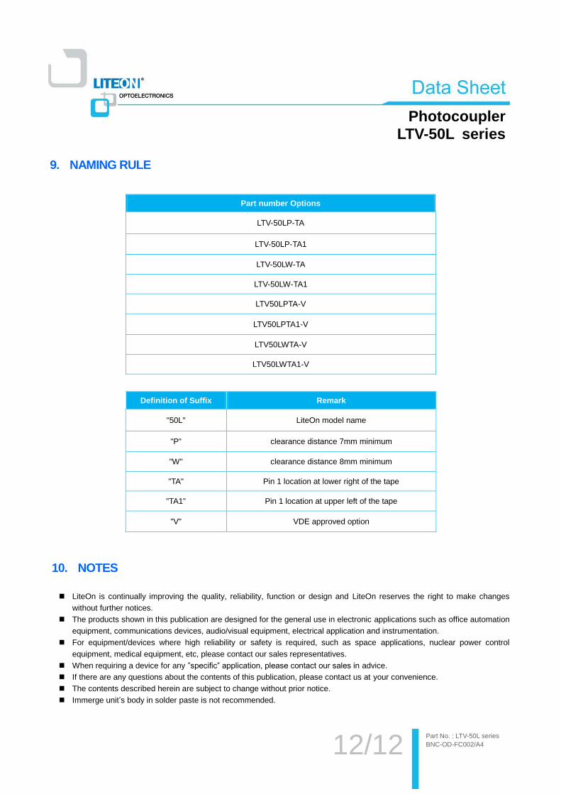
9. NAMING RULE
Part number Options
LTV-50LP-TA
LTV-50LP-TA1
LTV-50LW-TA
LTV-50LW-TA1
LTV50LPTA-V
LTV50LPTA1-V
LTV50LWTA-V
LTV50LWTA1-V
Definition of Suffix Remark
"50L" LiteOn model name
"P" clearance distance 7mm minimum
"W" clearance distance 8mm minimum
"TA" Pin 1 location at lower right of the tape
"TA1" Pin 1 location at upper left of the tape
"V" VDE approved option
10. NOTES
LiteOn is continually improving the quality, reliability, function or design and LiteOn reserves the right to make changes
without further notices.
The products shown in this publication are designed for the general use in electronic applications such as office automation
equipment, communications devices, audio/visual equipment, electrical application and instrumentation.
For equipment/devices where high reliability or safety is required, such as space applications, nuclear power control
equipment, medical equipment, etc, please contact our sales representatives.
When requiring a device for any ‖specific‖ application, please contact our sales in advice.
If there are any questions about the contents of this publication, please contact us at your convenience.
The contents described herein are subject to change without prior notice.
Immerge unit’s body in solder paste is not recommended.


![Polimetriche per linea da ATM STIBM - Autoguidoviemonzabrianza.autoguidovie.it/files/monzaBrianza/Polimetriche per lin… · 08**,2 ]rqh 0l 0l 021=$ ]rqh ]rqh 0l 0l 0l 0l %58*+(5,2](https://static.fdocuments.net/doc/165x107/6059bb1682314d00ec70cdd0/polimetriche-per-linea-da-atm-stibm-auto-per-lin-082-rqh-0l-0l-021-rqh.jpg)
