LTV-3150 series Product Data Sheet Photocoupler
15
LITE-ON DCC RELEASE BNS-OD-FC001/A4 LITE-ON Technology Corp. / Optoelectronics No.90,Chien 1 Road, Chung Ho, New Taipei City 23585, Taiwan, R.O.C. Tel: 886-2-2222-6181 Fax: 886-2-2221-1948 / 886-2-2221-0660 http://www.liteon.com/opto Photocoupler Product Data Sheet LTV-3150 series Spec No. :DS70-2012-0059 Effective Date: 06/23/2017 Revision: B
Transcript of LTV-3150 series Product Data Sheet Photocoupler
LITE-ON DCC
RELEASE
BNS-OD-FC001/A4
LITE-ON Technology Corp. / OptoelectronicsNo.90,Chien 1 Road, Chung Ho, New Taipei City 23585, Taiwan, R.O.C.
Tel: 886-2-2222-6181 Fax: 886-2-2221-1948 / 886-2-2221-0660http://www.liteon.com/opto
PhotocouplerProduct Data SheetLTV-3150 series
Spec No. :DS70-2012-0059Effective Date: 06/23/2017Revision: B
1/14
Photocouplers LTV-3150 series
Part No.: LTV-3150 series BNC-OD-FC002/A4 Rev.: B
1.0 Amp Output Current IGBT Gate Drive Optocoupler with Rail-to-Rail Output Voltage, High CMR.
1. DESCRIPTION The LTV-3150 optocoupler is ideally suited for driving power IGBTs and MOSFETs used in motor control inverter applications
and inverters in power supply system. It contains an AlGaAs LED optically coupled to an integrated circuit with a power output
stage. The 1.0A peak output current is capable of directly driving most IGBTs with ratings up to 1200 V/50 A. For IGBTs with higher
ratings, the LTV-3150 series can be used to drive a discrete power stage which drives the IGBT gate.
The Optocoupler operational parameters are guaranteed over the temperature range from -40oC ~ +105oC.
1.1 Features
� 1.0 A maximum peak output current
� Rail-to-rail output voltage
� 200 ns maximum propagation delay
� 100 ns maximum propagation delay difference
� 35 kV/us minimum Common Mode Rejection (CMR) at VCM = 1500 V
� ICC = 3.0 mA maximum supply current
� Wide operating range: 15 to 30 Volts (VCC)
� Guaranteed performance over temperature -40oC ~ +105oC.
� MSL Level 1
� Safety approval:
– UL/ cUL Recognized 5000 VRMS/1 min
– IEC/EN/DIN EN 60747-5-5 VIORM = 630 Vpeak
1.2 Applications
� IGBT/MOSFET gate drive
� Uninterruptible power supply (UPS)
� Industrial Inverter
� AC/Brushless DC motor drives
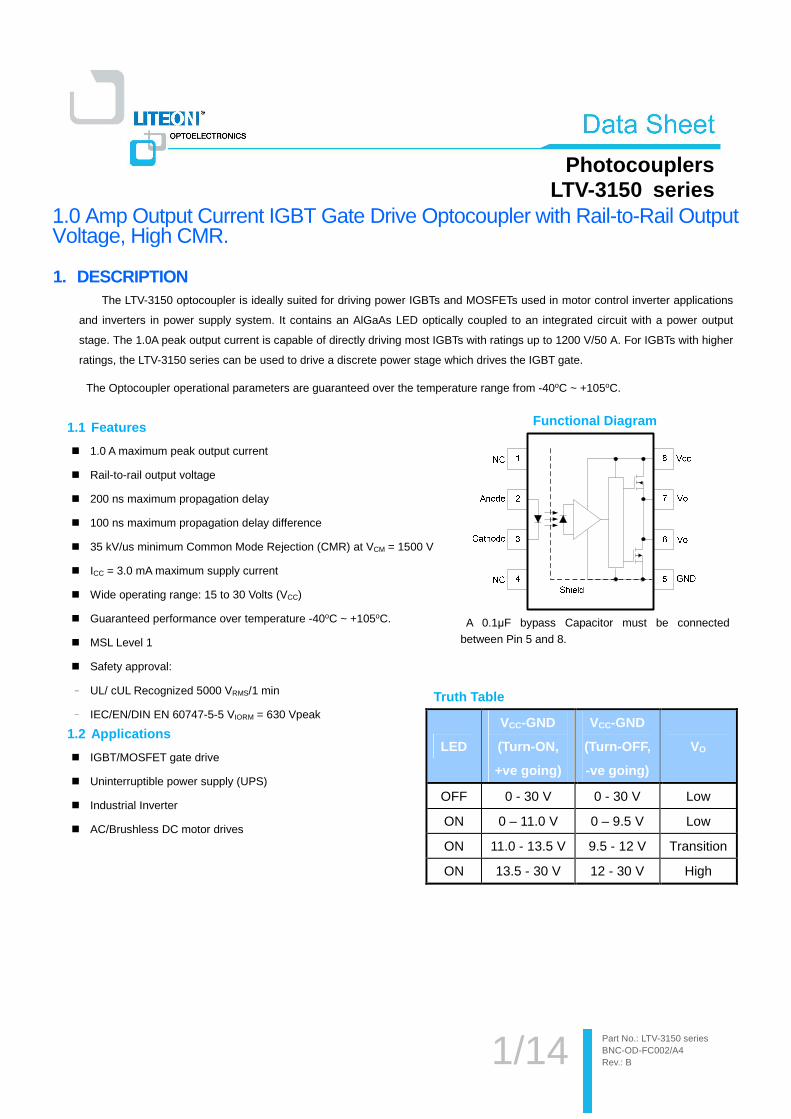
Truth Table
LED
VCC-GND
(Turn-ON,
+ve going)
VCC-GND
(Turn-OFF,
-ve going)
VO
OFF 0 - 30 V 0 - 30 V Low
ON 0 – 11.0 V 0 – 9.5 V Low
ON 11.0 - 13.5 V 9.5 - 12 V Transition
ON 13.5 - 30 V 12 - 30 V High
Functional Diagram
A 0.1μF bypass Capacitor must be connected
between Pin 5 and 8.
2/14
Photocouplers LTV-3150 series
Part No.: LTV-3150 series BNC-OD-FC002/A4 Rev.: B
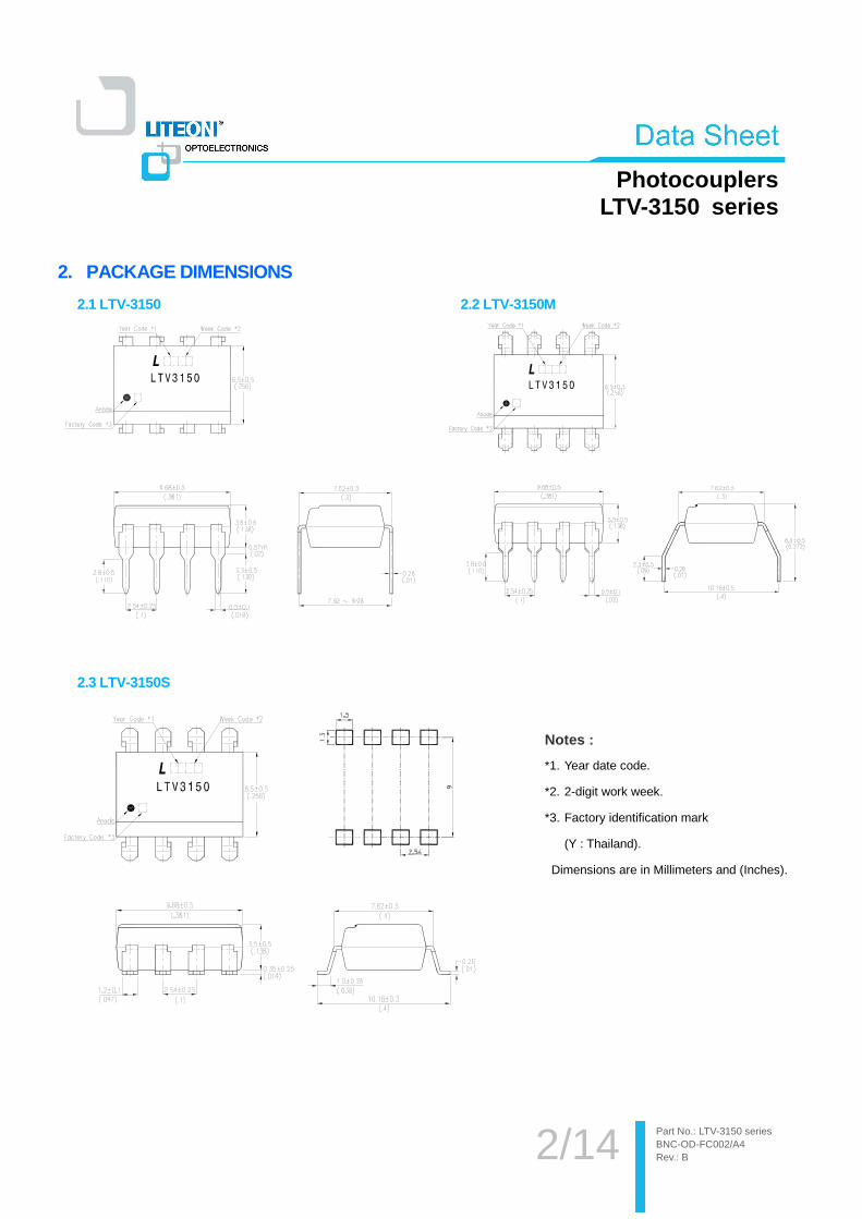
2. PACKAGE DIMENSIONS
2.1 LTV-3150 2.2 LTV-3150M
2.3 LTV-3150S
Notes :
*1. Year date code.
*2. 2-digit work week.
*3. Factory identification mark
(Y : Thailand).
Dimensions are in Millimeters and (Inches).
3/14
Photocouplers LTV-3150 series
Part No.: LTV-3150 series BNC-OD-FC002/A4 Rev.: B
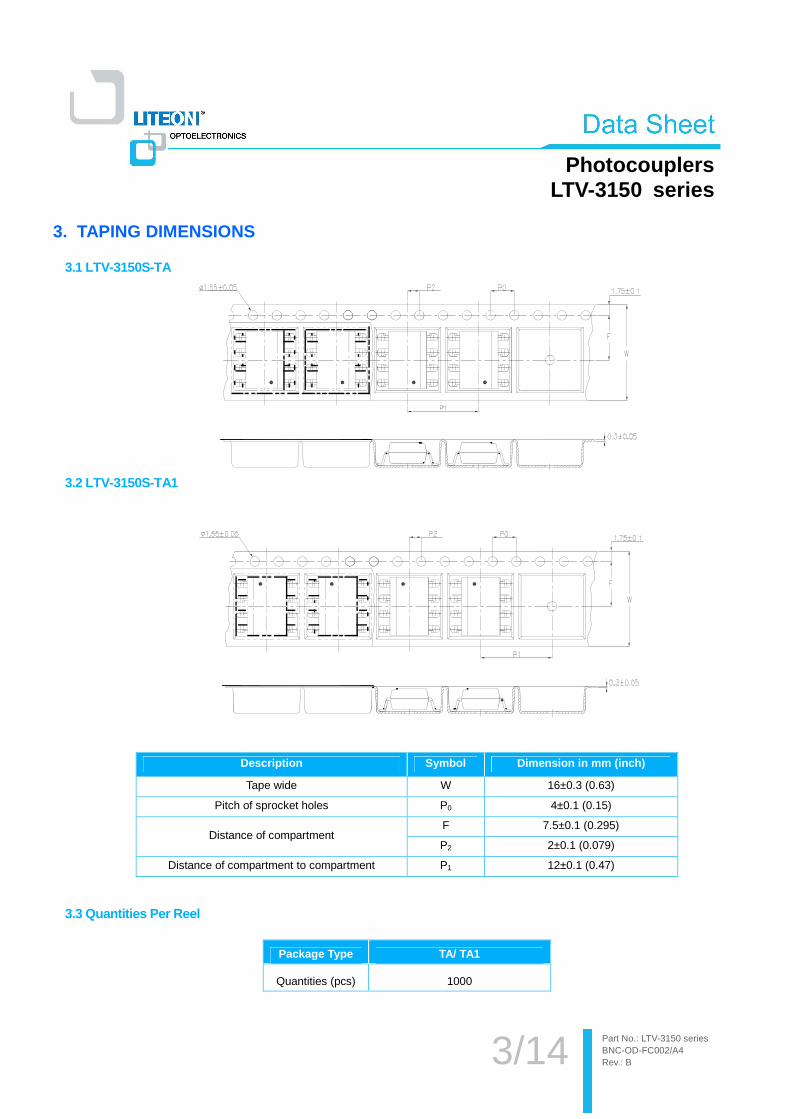
3. TAPING DIMENSIONS
3.1 LTV-3150S-TA
3.2 LTV-3150S-TA1
3.3 Quantities Per Reel
Description Symbol Dimension in mm (inch)
Tape wide W 16±0.3 (0.63)
Pitch of sprocket holes P0 4±0.1 (0.15)
Distance of compartment F 7.5±0.1 (0.295)
P2 2±0.1 (0.079)
Distance of compartment to compartment P1 12±0.1 (0.47)
Package Type TA/ TA1
Quantities (pcs) 1000
4/14
Photocouplers LTV-3150 series
Part No.: LTV-3150 series BNC-OD-FC002/A4 Rev.: B
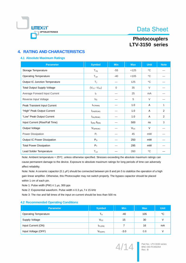
4. RATING AND CHARACTERISTICS 4.1 Absolute Maximum Ratings
Parameter Symbol Min Max Unit Note
Storage Temperature Tstg -55 +125 oC —
Operating Temperature Topr -40 +105 oC —
Output IC Junction Temperature TJ — 125 oC —
Total Output Supply Voltage (VCC –VEE) 0 35 V —
Average Forward Input Current IF — 25 mA —
Reverse Input Voltage VR — 5 V —
Peak Transient Input Current IF(TRAN) — 1.0 A 1
“High” Peak Output Current IOH(PEAK) — 1.0 A 2
“Low” Peak Output Current IOL(PEAK) — 1.0 A 2
Input Current (Rise/Fall Time) tr(IN) /tf(IN) — 500 ns 3
Output Voltage VO(PEAK) — VCC V —
Power Dissipation PI — 45 mW —
Output IC Power Dissipation PO — 250 mW —
Total Power Dissipation PT — 295 mW —
Lead Solder Temperature Tsol — 260 oC —
Note: Ambient temperature = 25oC, unless otherwise specified. Stresses exceeding the absolute maximum ratings can
cause permanent damage to the device. Exposure to absolute maximum ratings for long periods of time can adversely
affect reliability.
Note: Note: A ceramic capacitor (0.1 μF) should be connected between pin 8 and pin 5 to stabilize the operation of a high
gain linear amplifier. Otherwise, this Photocoupler may not switch properly. The bypass capacitor should be placed
within 1 cm of each pin.
Note 1: Pulse width (PW) ≤ 1 μs, 300 pps
Note 2: Exponential waveform. Pulse width ≤ 0.3 μs, f ≤ 15 kHz
Note 3: The rise and fall times of the input on-current should be less than 500 ns
4.2 Recommended Operating Conditions
Parameter Symbol Min Max Unit
Operating Temperature TA -40 105 oC
Supply Voltage VCC 15 30 V
Input Current (ON) IFL(ON) 7 16 mA
Input Voltage (OFF) VF(OFF) -3.0 0.8 V
5/14
Photocouplers LTV-3150 series
Part No.: LTV-3150 series BNC-OD-FC002/A4 Rev.: B
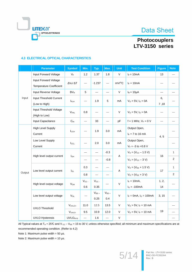
4.3 ELECTRICAL OPTICAL CHARACTERISTICS
Parameter Symbol Min. Typ. Max. Unit Test Condition Figure Note
Input
Input Forward Voltage VF 1.2 1.37 1.8 V IF = 10mA 13 —
Input Forward Voltage
Temperature Coefficient ΔVF/ ΔT — -1.237 — mV/OC IF = 10mA — —
Input Reverse Voltage BVR 5 — — V IR = 10μA — —
Input Threshold Current
(Low to High) IFLH — 1.9 5 mA VO > 5V, IO = 0A
6,
7 ,18 —
Input Threshold Voltage
(High to Low) VFHL 0.8 — — V VO < 5V, IO = 0A — —
Input Capacitance CIN — 33 — pF f = 1 MHz, VF = 0 V — —
Output
High Level Supply
Current ICCH — 1.9 3.0 mA
Output Open,
IF = 7 to 16 mA 4, 5
—
Low Level Supply
Current ICCL — 2.0 3.0 mA
Output Open,
VF = -3 to +0.8 V —
High level output current IOH — — -0.3
A VO = (VCC – 1.5 V)
16 1
— — -0.8 VO = (VCC – 3 V) 2
Low level output current IOL 0.3 — —
A VO = (VEE + 1.5 V)
17 1
0.8 — — VO = (VEE + 3 V) 2
High level output voltage VOH VCC -
0.6
VCC -
0.35 — V
IF = 10mA,
IO = -100mA
1, 2,
14 —
Low level output voltage VOL — VEE +
0.25
VEE +
0.4 V IF = 0mA, IO = 100mA 3, 15 —
UVLO Threshold VUVLO+ 11.0 12.5 13.5 V VO > 5V, IF = 10 mA
19
—
VUVLO- 9.5 10.9 12.0 V VO < 5V, IF = 10 mA —
UVLO Hysteresis UVLOHYS — 1.6 — V —
All Typical values at TA = 25°C and V CC – VEE = 15 to 30 V, unless otherwise specified; all minimum and maximum specifications are at
recommended operating condition. (Refer to 4.2)
Note 1: Maximum pulse width = 50 μs.
Note 2: Maximum pulse width = 10 μs.

6/14
Photocouplers LTV-3150 series
Part No.: LTV-3150 series BNC-OD-FC002/A4 Rev.: B
5. SWITCHING SPECIFICATION
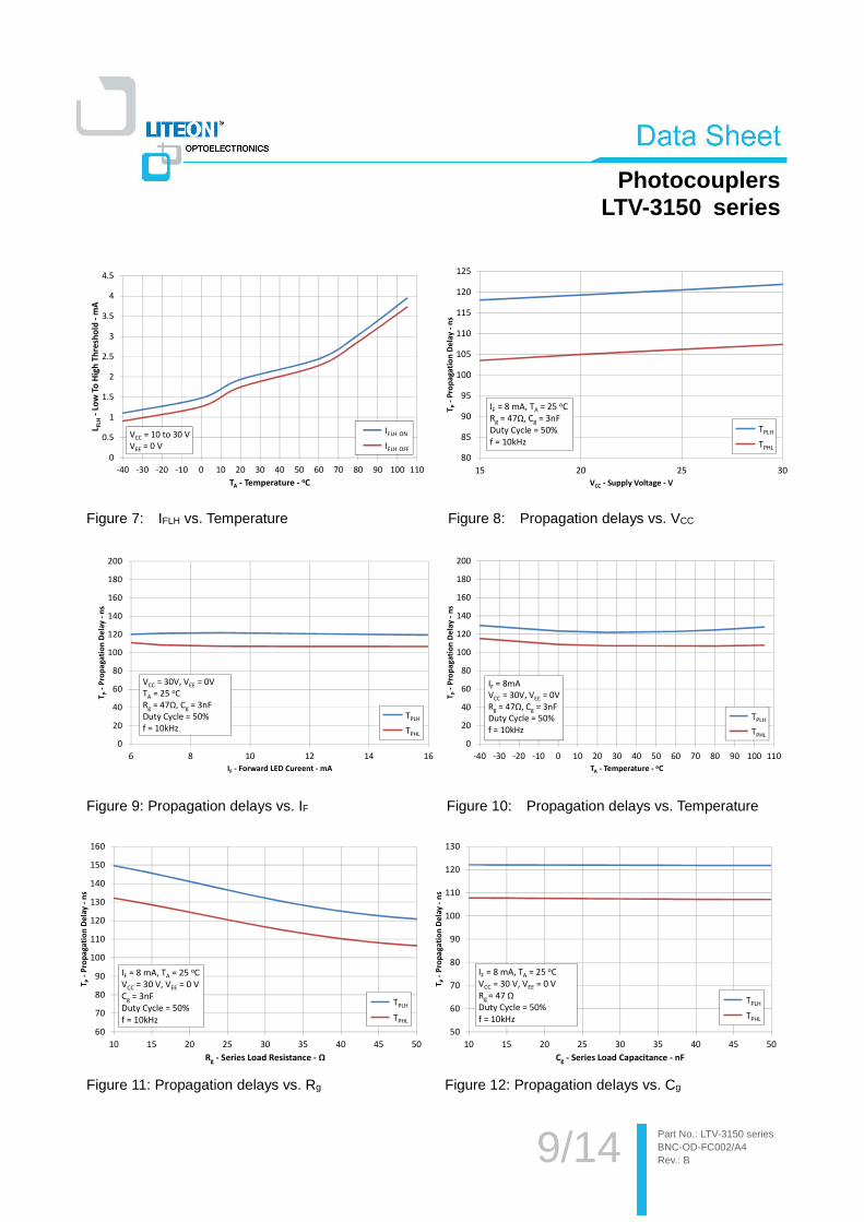
Parameter Symbol Min. Typ. Max. Unit Test Condition Figure Note
Propagation Delay Time to
High Output Level tPLH 50 120 200
ns
Rg = 47Ω,
Cg = 3nF,
f = 10 kHz,
Duty Cycle = 50%
IF = 7 to 16 mA,
VCC = 15 to 30V
VEE = ground
8, 9, 10,
11, 12,
20
—
Propagation Delay Time to
Low Output Level tPHL 50 110 200 —
Pulse Width Distortion PWD — 15 70 —
Propagation delay difference
between any two parts or
channels
PDD -100 — 100 3
Output Rise Time (20 to 80%) Tr — 35 — 20
—
Output Fall Time (80 to 20%) Tf — 35 — —
UVLO turn on delay TUVLO ON — 1.6 —
μs
IF = 10 mA,
VO > 5 V —
UVLO turn off delay TUVLO OFF — 0.4 — IF = 10 mA,
VO < 5 V —
Common mode transient
immunity at high level output |CMH| 35 50 — kV/μs
TA = 25°C,
IF = 10 to 16 mA,
VCM = 1500 V,
VCC = 30 V 21
1
Common mode transient
immunity at low level output |CML| 35 50 — kV/μs
TA = 25°C,
VF = 0 V,
VCM = 1500 V,
VCC = 30 V
2
All Typical values at TA = 25°C and V CC – VEE = 15 to 30 V, unless otherwise specified; all minimum and maximum specifications are
at recommended operating condition. (Refer to 4.2)
Note 1: CMH is the maximum rate of rise of the common mode voltage that can be sustained with the output voltage in the logic high
state (VO > 15 V).
Note 2: CML is the maximum rate of fall of the common mode voltage that can be sustained with the output voltage in the logic low
state (VO < 1 V).
Note 3: The difference between tPHL and tPLH between any two parts series parts under same test conditions.
7/14
Photocouplers LTV-3150 series
Part No.: LTV-3150 series BNC-OD-FC002/A4 Rev.: B
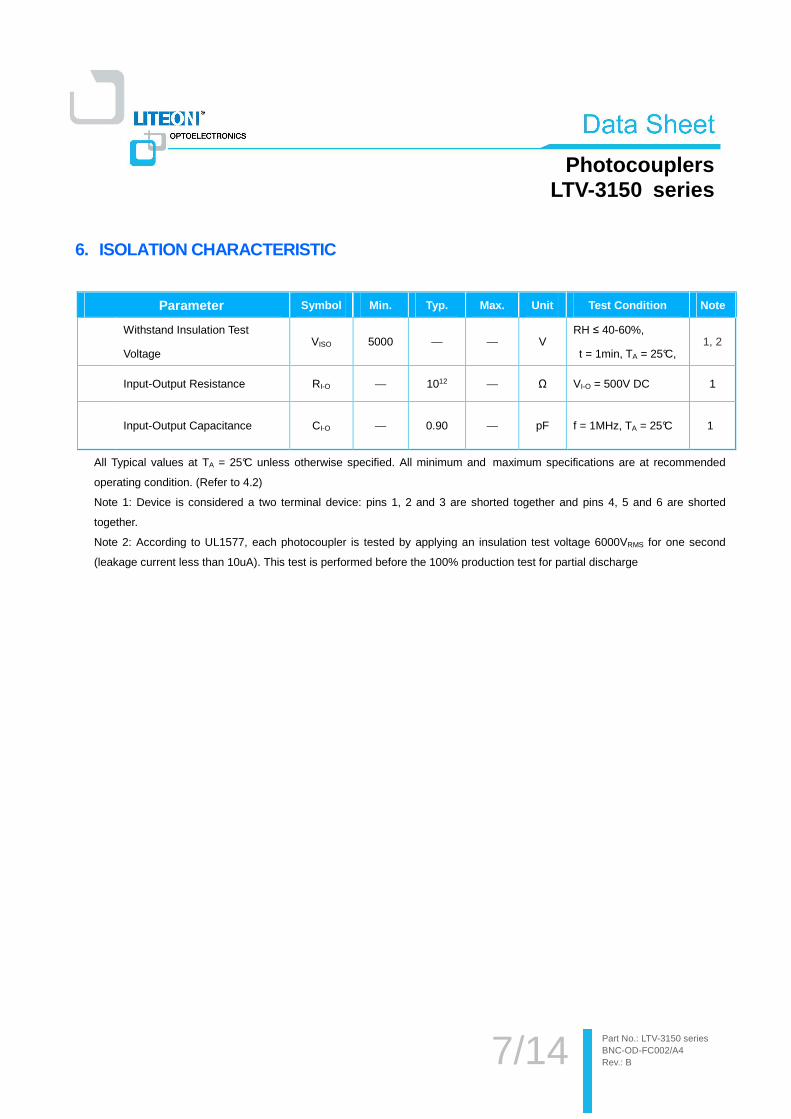
6. ISOLATION CHARACTERISTIC
Parameter Symbol Min. Typ. Max. Unit Test Condition Note
Withstand Insulation Test
Voltage VISO 5000 — — V
RH ≤ 40-60%,
t = 1min, TA = 25°C, 1, 2
Input-Output Resistance RI-O — 1012 — Ω VI-O = 500V DC 1
Input-Output Capacitance CI-O — 0.90 — pF f = 1MHz, TA = 25°C 1
All Typical values at TA = 25°C unless otherwise specified. All minimum and maximum specifications are at recommended
operating condition. (Refer to 4.2)
Note 1: Device is considered a two terminal device: pins 1, 2 and 3 are shorted together and pins 4, 5 and 6 are shorted
together.
Note 2: According to UL1577, each photocoupler is tested by applying an insulation test voltage 6000VRMS for one second
(leakage current less than 10uA). This test is performed before the 100% production test for partial discharge
8/14
Photocouplers LTV-3150 series
Part No.: LTV-3150 series BNC-OD-FC002/A4 Rev.: B
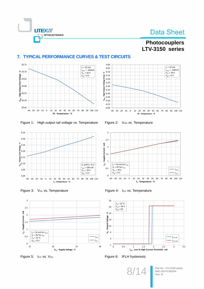
7. TYPICAL PERFORMANCE CURVES & TEST CIRCUITS
29.45
29.50
29.55
29.60
29.65
29.70
29.75
-40 -30 -20 -10 0 10 20 30 40 50 60 70 80 90 100 110
VO
H-
Hig
h O
utp
ut
Ra
il V
olt
ag
e -
V
TA - Temperature - oC
IF = 10 mA
IOUT = -100mA
VCC = 30 V
VEE = 0 V
-0.60
-0.55
-0.50
-0.45
-0.40
-0.35
-0.30
-0.25
-0.20
-0.15
-0.10
-0.05
0.00
-40 -30 -20 -10 0 10 20 30 40 50 60 70 80 90 100 110
VO
H-
Hig
h O
utp
ut
Vo
lta
ge
Dro
p -
V
TA - Temperature - oC
IF = 10 mA
IOUT = -100mA
VCC = 30 V
VEE = 0 V
Figure 1: High output rail voltage vs. Temperature Figure 2: VOH vs. Temperature
0.00
0.05
0.10
0.15
0.20
0.25
0.30
0.35
-40 -30 -20 -10 0 10 20 30 40 50 60 70 80 90 100 110
VO
L-
Ou
tpu
t Lo
w V
olt
ag
e -
V
TA - Temperature - oC
VF (OFF) = 0 V
Iout = 100 mA
VCC = 30 V
VEE = 0 V
0
0.5
1
1.5
2
2.5
3
-40 -30 -20 -10 0 10 20 30 40 50 60 70 80 90 100 110
I CC
-S
up
ply
Cu
rre
nt
-m
A
TA - Tamperature - oC
IF = 10 mA for ICCH
VF = 0V for ICCL
VCC = 30 V
VEE = 0 V ICCL
ICCH
Figure 3: VOL vs. Temperature Figure 4: ICC vs. Temperature
0
0.5
1
1.5
2
2.5
3
15 20 25 30
I CC
-S
up
ply
Cu
rre
nt
-m
A
VCC - Supply Voltage - V
ICCL
ICCH
IF = 10 mA for ICCH
VF = 0V for ICCL
TA = 25 oC
VEE = 0 V
-1
4
9
14
19
24
29
34
0 0.5 1 1.5 2 2.5 3 3.5
VO
-O
utp
ut
Vo
lta
ge
-V
IFLH - Low To High Current Threshold - mA
IFLH OFF
IFLH ON
TA = 25 oC
VCC = 30 V
VEE = 0V
Figure 5: ICC vs. VCC Figure 6: IFLH hysteresis
9/14
Photocouplers LTV-3150 series
Part No.: LTV-3150 series BNC-OD-FC002/A4 Rev.: B
0
0.5
1
1.5
2
2.5
3
3.5
4
4.5
-40 -30 -20 -10 0 10 20 30 40 50 60 70 80 90 100 110
LFLH
-Lo
w T
o H
igh
Th
resh
old
-m
A
TA - Temperature - oC
VCC = 10 to 30 V
VEE = 0 V IFLH OFF
IFLH ON
80
85
90
95
100
105
110
115
120
125
15 20 25 30
TP
-P
rop
aga
tio
n D
ela
y -
ns
VCC - Supply Voltage - V
IF = 8 mA, TA = 25 oC
Rg = 47Ω, Cg = 3nF
Duty Cycle = 50%
f = 10kHz TPHL
TPLH
Figure 7: IFLH vs. Temperature Figure 8: Propagation delays vs. VCC
0
20
40
60
80
100
120
140
160
180
200
6 8 10 12 14 16
TP
-P
rop
aga
tio
n D
ela
y -
ns
IF - Forward LED Cureent - mA
VCC = 30V, VEE = 0V
TA = 25 oC
Rg = 47Ω, Cg = 3nF
Duty Cycle = 50%
f = 10kHz TPHL
TPLH
0
20
40
60
80
100
120
140
160
180
200
-40 -30 -20 -10 0 10 20 30 40 50 60 70 80 90 100 110
TP
-P
rop
ag
ati
on
De
lay
-n
s
TA - Temperature - oC
IF = 8mA
VCC = 30V, VEE = 0V
Rg = 47Ω, Cg = 3nF
Duty Cycle = 50%
f = 10kHz TPHL
TPLH
Figure 9: Propagation delays vs. IF Figure 10: Propagation delays vs. Temperature
60
70
80
90
100
110
120
130
140
150
160
10 15 20 25 30 35 40 45 50
TP
-P
rop
ag
ati
on
De
lay
-n
s
Rg - Series Load Resistance - Ω
TPHL
TPLH
IF = 8 mA, TA = 25 oC
VCC = 30 V, VEE = 0 V
Cg = 3nF
Duty Cycle = 50%
f = 10kHz
50
60
70
80
90
100
110
120
130
10 15 20 25 30 35 40 45 50
TP
-P
rop
ag
ati
on
De
lay
-n
s
Cg - Series Load Capacitance - nF
IF = 8 mA, TA = 25 oC
VCC = 30 V, VEE = 0 V
Rg = 47 Ω
Duty Cycle = 50%
f = 10kHz TPHL
TPLH
Figure 11: Propagation delays vs. Rg Figure 12: Propagation delays vs. Cg
10/14
Photocouplers LTV-3150 series
Part No.: LTV-3150 series BNC-OD-FC002/A4 Rev.: B
10
20
30
40
50
60
1.4 1.45 1.5 1.55 1.6
I F-
Fo
rwa
rd C
urr
en
t -
mA
VF - Forward Voltage - V
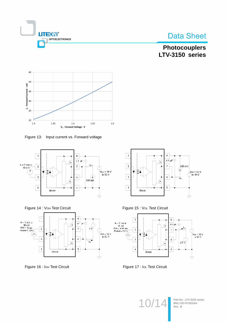
Figure 13: Input current vs. Forward voltage
Figure 14 : VOH Test Circuit Figure 15 : VOL Test Circuit
Figure 16 : IOH Test Circuit Figure 17 : IOL Test Circuit
11/14
Photocouplers LTV-3150 series
Part No.: LTV-3150 series BNC-OD-FC002/A4 Rev.: B
I F
V >5VO
+-
0.1uF
=15V to 30VVCC
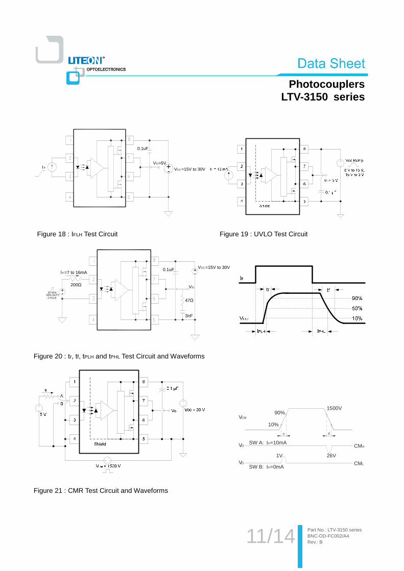
Figure 18 : IFLH Test Circuit Figure 19 : UVLO Test Circuit
I F
VO
+-
47Ω
3nF
0.1uF =7 to 16mA
200Ω +-10 KHz
50% DUTYCYCLE
=15V to 30VVCC
Figure 20 : tr, tf, tPLH and tPHL Test Circuit and Waveforms
VCM
VO
90%
10%
tr tf
1500V
SW A: IF=10mA
26V1V
CMH
CMLSW B: IF=0mA
VO
Figure 21 : CMR Test Circuit and Waveforms
12/14
Photocouplers LTV-3150 series
Part No.: LTV-3150 series BNC-OD-FC002/A4 Rev.: B
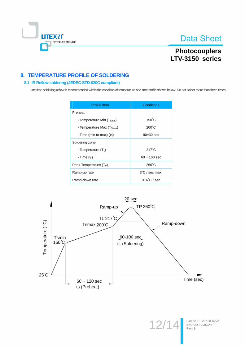
8. TEMPERATURE PROFILE OF SOLDERING
8.1 IR Reflow soldering (JEDEC-STD-020C compliant)
One time soldering reflow is recommended within the condition of temperature and time profile shown below. Do not solder more than three times.
Profile item Conditions
Preheat
- Temperature Min (TSmin)
- Temperature Max (TSmax)
- Time (min to max) (ts)
150˚C
200˚C
90±30 sec
Soldering zone
- Temperature (TL)
- Time (tL)
217˚C
60 ~ 100 sec
Peak Temperature (TP) 260˚C
Ramp-up rate 3˚C / sec max.
Ramp-down rate 3~6˚C / sec
60 ~ 120 sec25 C
150 C
200 C
260 C
217 C
60-100 sec
Time (sec)
Tem
pera
ture
( C
)
20 sec
Tsmax
ts (Preheat)
tL (Soldering)Tsmin
TL
TP
Ramp-down
Ramp-up
13/14
Photocouplers LTV-3150 series
Part No.: LTV-3150 series BNC-OD-FC002/A4 Rev.: B
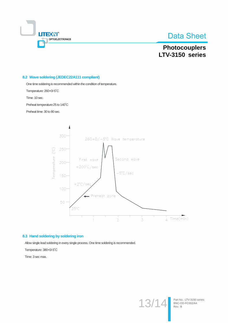
8.2 Wave soldering (JEDEC22A111 compliant)
One time soldering is recommended within the condition of temperature.
Temperature: 260+0/-5˚C
Time: 10 sec.
Preheat temperature:25 to 140˚C
Preheat time: 30 to 80 sec.
8.3 Hand soldering by soldering iron
Allow single lead soldering in every single process. One time soldering is recommended.
Temperature: 380+0/-5˚C
Time: 3 sec max.
14/14
Photocouplers LTV-3150 series
Part No.: LTV-3150 series BNC-OD-FC002/A4 Rev.: B
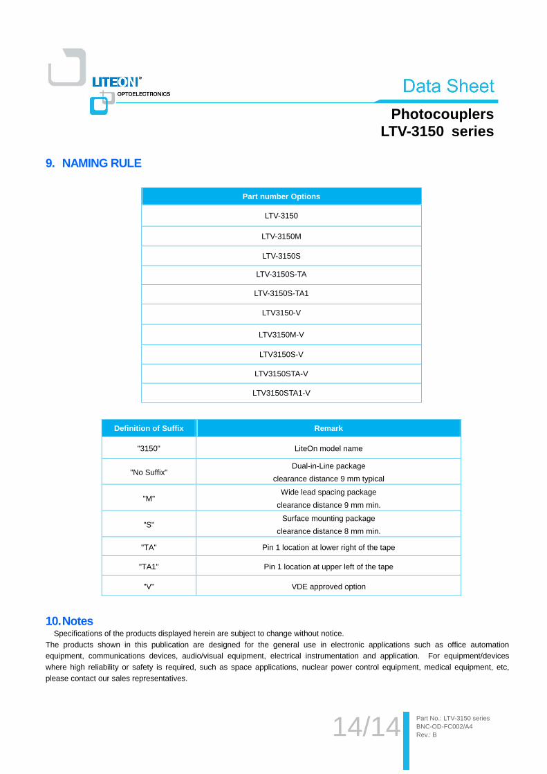
9. NAMING RULE
Part number Options
LTV-3150
LTV-3150M
LTV-3150S
LTV-3150S-TA
LTV-3150S-TA1
LTV3150-V
LTV3150M-V
LTV3150S-V
LTV3150STA-V
LTV3150STA1-V
Definition of Suffix Remark
"3150" LiteOn model name
"No Suffix" Dual-in-Line package
clearance distance 9 mm typical
"M" Wide lead spacing package
clearance distance 9 mm min.
"S" Surface mounting package
clearance distance 8 mm min.
"TA" Pin 1 location at lower right of the tape
"TA1" Pin 1 location at upper left of the tape
"V" VDE approved option
10. Notes
Specifications of the products displayed herein are subject to change without notice. The products shown in this publication are designed for the general use in electronic applications such as office automation equipment, communications devices, audio/visual equipment, electrical instrumentation and application. For equipment/devices where high reliability or safety is required, such as space applications, nuclear power control equipment, medical equipment, etc, please contact our sales representatives.