Low Voltage Organic Field Effect Transistors for Printed Electronics
18
Low Voltage Organic Field-Effect Transistors for Printed Electronics June 2014 to August 2014 Supervisor-Dr. Leszek Majewski Microelectronics and Nanostructure Group School of Electrical and Electronic Engineering The University of Manchester Vishisht M. Tiwari (Year-1 Undergraduate)
-
Upload
vishisht-tiwari -
Category
Engineering
-
view
141 -
download
4
Transcript of Low Voltage Organic Field Effect Transistors for Printed Electronics
Low Voltage Organic Field-Effect Transistors for Printed Electronics
June 2014 to August 2014
Supervisor-Dr. Leszek Majewski Microelectronics and Nanostructure Group
School of Electrical and Electronic Engineering The University of Manchester
Vishisht M. Tiwari (Year-1 Undergraduate)
II
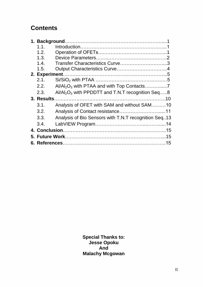
Contents 1. Background…………………………………………………….....1
1.1. Introduction……………………………………………....1 1.2. Operation of OFETs….………………………….….…..1 1.3. Device Parameters……..……………………………….2 1.4. Transfer Characteristics Curve………………………...3 1.5. Output Characteristics Curve…………………………..4
2. Experiment………………………………………………………...5 2.1. Si/SiO2 with PTAA ………………………………………5
2.2. Al/Al2O3 with PTAA and with Top Contacts………......7
2.3. Al/Al2O3 with PPDDTT and T.N.T recognition Seq…..8
3. Results…………………………………………………………….10
3.1. Analysis of OFET with SAM and without SAM………10
3.2. Analysis of Contact resistance……………………......11
3.3. Analysis of Bio Sensors with T.N.T recognition Seq..13
3.4. LabVIEW Program…………………………....……......14
4. Conclusion………………………………………………………..15
5. Future Work……………………………………………………....15
6. References………………………………………………………..15
Special Thanks to: Jesse Opoku
And Malachy Mcgowan
1
Background
Introduction
The field of nanoelectronics and microstructures has seen some great
inventions in the past few decades. One such invention is the development of
the Organic Field Effect Transistors (OFETs). These transistors have provided
the basic building block for flexible integrated circuits and displays. Intensive
research is being carried out almost everyday in this field and more and more
viable options are being prepared for industry purposes. Working in this field has
helped me to gain valuable knowledge about this upcoming subject and also
helped me broaden my horizon about other fields that are connected to
nanostructures and microelectronics.
Operation of OFETs
An Organic field-effect transistor (OFET) is a field effect transistor that uses
organic semiconductors in its channel. OFETs can be prepared by either
electro-polymerisation, by solution-based deposition of polymers, by vacuum
evaporation of small molecules or by Langmuir-Blodgett Technique. These
devices have many advantages over its non-organic counterparts such as easy
fabrication, mechanical flexibility, biodegradability and lower cost.
There are 3 different geometries in which FETs can be used:
The MISFET- Metal-Insulator-Semiconductor Junction
The MESFET- Metal-Semiconductor Field Effect Transistor
The TFT- Thin-Film Transistor
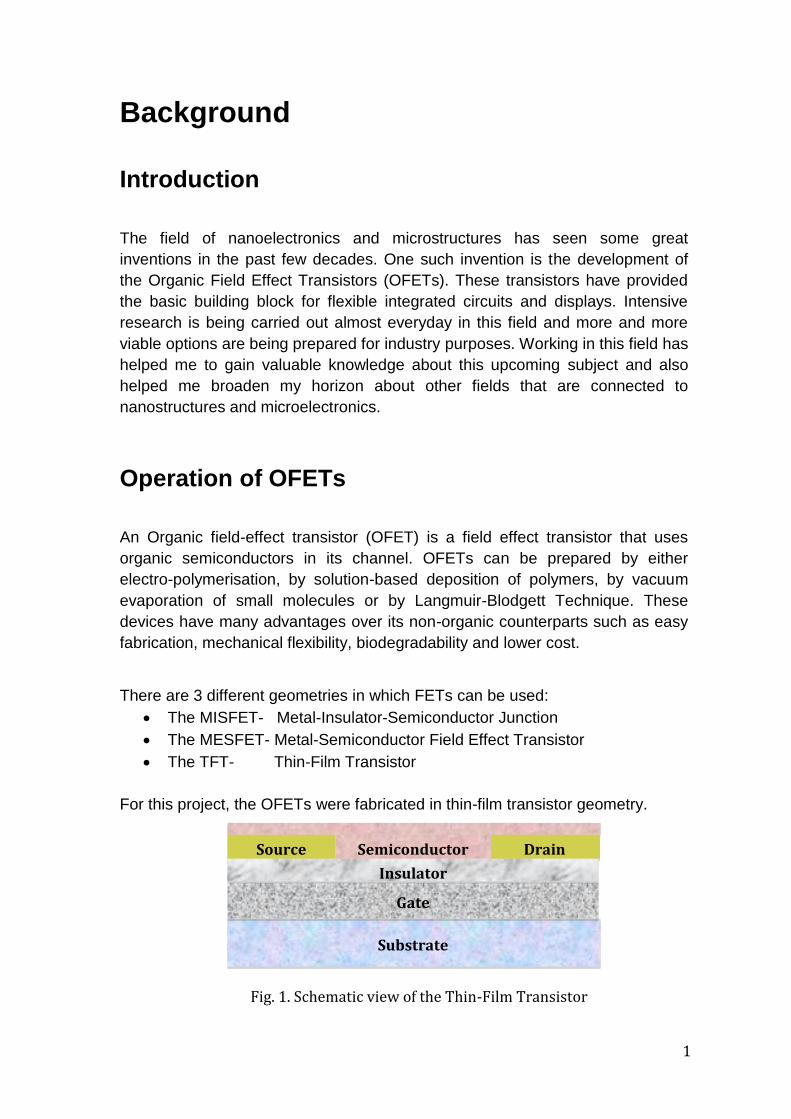
For this project, the OFETs were fabricated in thin-film transistor geometry.
Substrate
Gate
Insulator
Source Drain Semiconductor
Fig. 1. Schematic view of the Thin-Film Transistor
2
In this geometry, the source electrode and drain electrode are deposited on the
thin film of insulator. This layer of insulator separates the gate from the
electrodes. The layer of semiconductor is then deposited on the insulator and
electrodes.
Unlike in other geometries, TFTs operate in accumulation regime rather than in
the inversion regime and there is no depletion region to isolate the device from
the substrate. On applying a zero bias, the electrons are expelled from the
surface due to difference in the Fermi-level of the semiconductor and the metal.
In this case, no carrier movement is observed between the source and drain. On
applying a positive charge, the conduction band bends downward forming a very
conductive channel on the interface.
Device Parameters
Parameters are empirical properties of OFETs that define how well a transistor
can work by showing its different electrical properties. Most of these parameters
can be derived by observing transfer and output characteristics of the transistor.
Few of the important parameters are as follows:
MOBILITY-Mobility is the measure of ease with which holes can move from the
source to the drain when electric field is applied. Mobility of an OFET, in both
linear region and saturation region, can be calculated using different properties
of the transistor such as drain current (ID), width of the channel (W), length of the
channel (L) and gate voltage (VG). The formula for calculating mobility is as
follows:
Linear Mobility
Saturation Mobility
ON-OFF CURRENT RATIO-It is the ratio of the value of the current when the
device saturates to that value of the current when the device is not switched on.
This ratio can be calculated using the transfer characteristics curve.
ONSET VOLTAGE-The gate voltage at which the transistor starts to conduct is
called the onset voltage. This parameter can also be calculated using transfer
3
characteristic curve. At this voltage the current starts to increase exponentially.
SUBTHRESHOLD SLOPE- Subthreshold slope shows the change in drain
current (ID) with unit change in gate voltage (VG) it can be calculated by
calculating the slope of the transfer characteristic curve of a transistor. The
voltage is plotted on the x-axis while the current is plotted on the y-axis in
logarithmic form. The formula can be represented as follows:
TRANSCONDUCTANCE-Transconductance relates the transistor output
current with the input gate voltage. It is defines as the rate of change of drain
current with respect to the gate voltage. This parameter can be calculated using
the transfer characteristics curve. However it can also be calculated
mathematically by using width (W) and length of the channel (L), capacitance of
the transistor (C) and the mobility of the transistor. The formula can be
represented as follows:
OPERATING VOLTAGE-Operating Voltage is the peak gate voltage till which
the device can be used as a transistor. It is sometimes also referred to as the
breakdown voltage because the transistor can breakdown if this voltage is
exceeded.
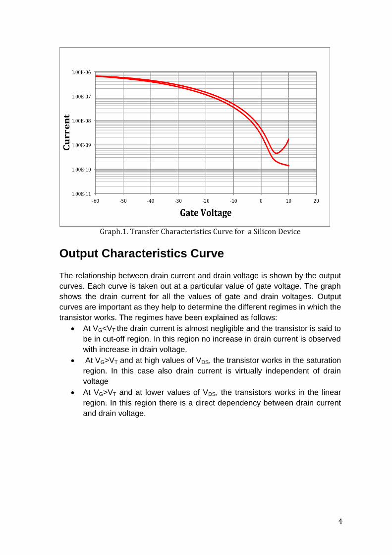
Transfer Characteristics Curve
To understand how well a transistor is working, the relation between the
controlling variable and the controlled variable has to be established. Transfer
characteristics help to derive this relation. The curve shows the dependence of
drain current over a range of values of gate voltage. Conclusions that can be
drawn out from the transfer characteristic curves are as follows:
Drain current is almost zero when gate voltage is less than the threshold
voltage.
The voltage from where the current starts to rise is the onset voltage.
Once the transistor starts to conduct, the current increases exponentially.
The ratio of the current at the highest point to the current at the lowest
point can give us the on-off ratio.
Subthreshold slope can be derived by finding the slope of the transfer
characteristics curve.
4
Graph.1. Transfer Characteristics Curve for a Silicon Device
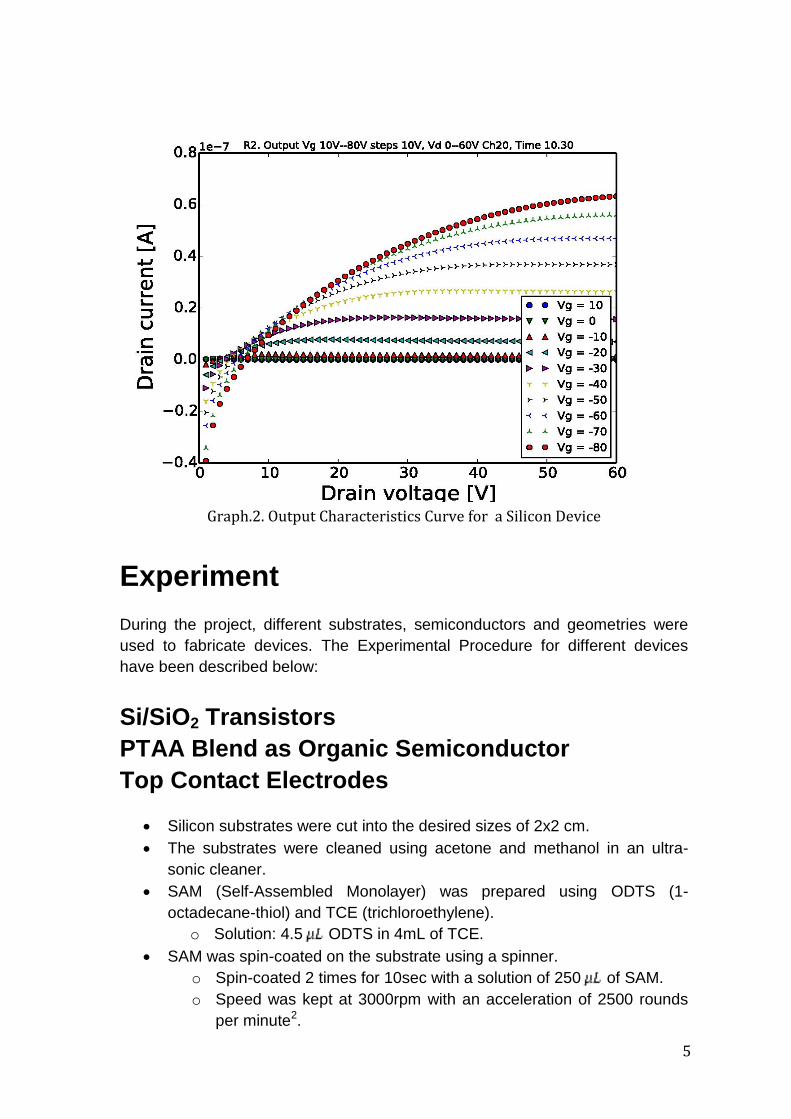
Output Characteristics Curve
The relationship between drain current and drain voltage is shown by the output
curves. Each curve is taken out at a particular value of gate voltage. The graph
shows the drain current for all the values of gate and drain voltages. Output
curves are important as they help to determine the different regimes in which the
transistor works. The regimes have been explained as follows:
At VG<VT the drain current is almost negligible and the transistor is said to
be in cut-off region. In this region no increase in drain current is observed
with increase in drain voltage.
At VG>VT and at high values of VDS, the transistor works in the saturation
region. In this case also drain current is virtually independent of drain
voltage
At VG>VT and at lower values of VDS, the transistors works in the linear
region. In this region there is a direct dependency between drain current
and drain voltage.
5
Graph.2. Output Characteristics Curve for a Silicon Device
Experiment
During the project, different substrates, semiconductors and geometries were
used to fabricate devices. The Experimental Procedure for different devices
have been described below:
Si/SiO2 Transistors
PTAA Blend as Organic Semiconductor
Top Contact Electrodes
Silicon substrates were cut into the desired sizes of 2x2 cm.
The substrates were cleaned using acetone and methanol in an ultra-
sonic cleaner.
SAM (Self-Assembled Monolayer) was prepared using ODTS (1-
octadecane-thiol) and TCE (trichloroethylene).
o Solution: 4.5 ODTS in 4mL of TCE.
SAM was spin-coated on the substrate using a spinner.
o Spin-coated 2 times for 10sec with a solution of 250 of SAM.
o Speed was kept at 3000rpm with an acceleration of 2500 rounds
per minute2.
6
The substrate was then annealed at 105 oC for 20min.
After annealing, the substrate was cleaned again in an ultrasonic cleaner
using methanol and IPA (isopropyl alcohol).
PTAA was used as the organic semiconductor.
o Solution: 10mg of PTAA in 1ml of 12-
dochlorobenzene.
A layer of this PTAA was spin-coated on the
substrate using a spinner.
o Spin-coated for 1min with a solution of
250 of PTAA
o Speed was kept at 2000rpm with an
acceleration of 255 rounds per
minute2.
The substrate was again annealed but this
time at 100 oC for an hour.
The environment was ensured to be oxygen
free.
Gold was cleaned in an ultrasonic cleaner
using acetone and methanol
Gold was then evaporated on the substrate for drain and source
electrodes.
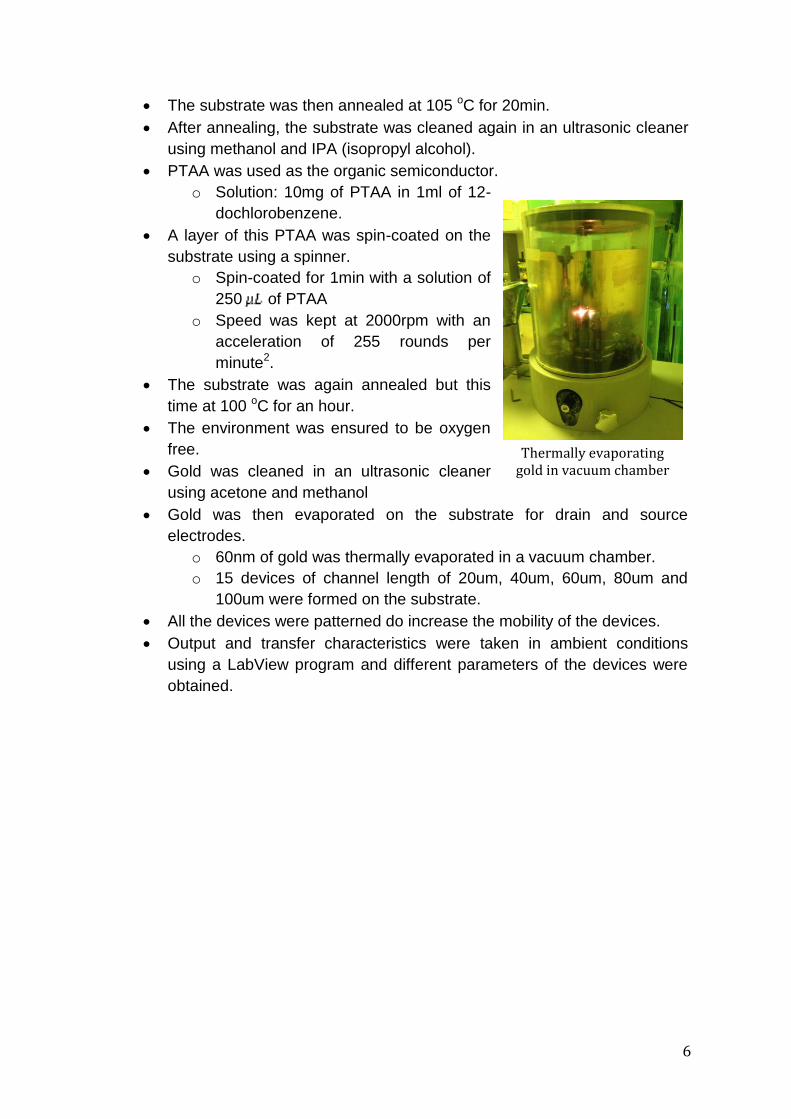
o 60nm of gold was thermally evaporated in a vacuum chamber.
o 15 devices of channel length of 20um, 40um, 60um, 80um and
100um were formed on the substrate.
All the devices were patterned do increase the mobility of the devices.
Output and transfer characteristics were taken in ambient conditions
using a LabView program and different parameters of the devices were
obtained.
Thermally evaporating gold in vacuum chamber
7
Al/Al2O3 Transistors
PTAA Blend as Organic Semiconductor
Top Contact Electrodes
Glass substrates were cut into the desired sizes of 2x2 cm.
The substrates were cleaned using acetone and methanol in an
ultra- sonic cleaner.
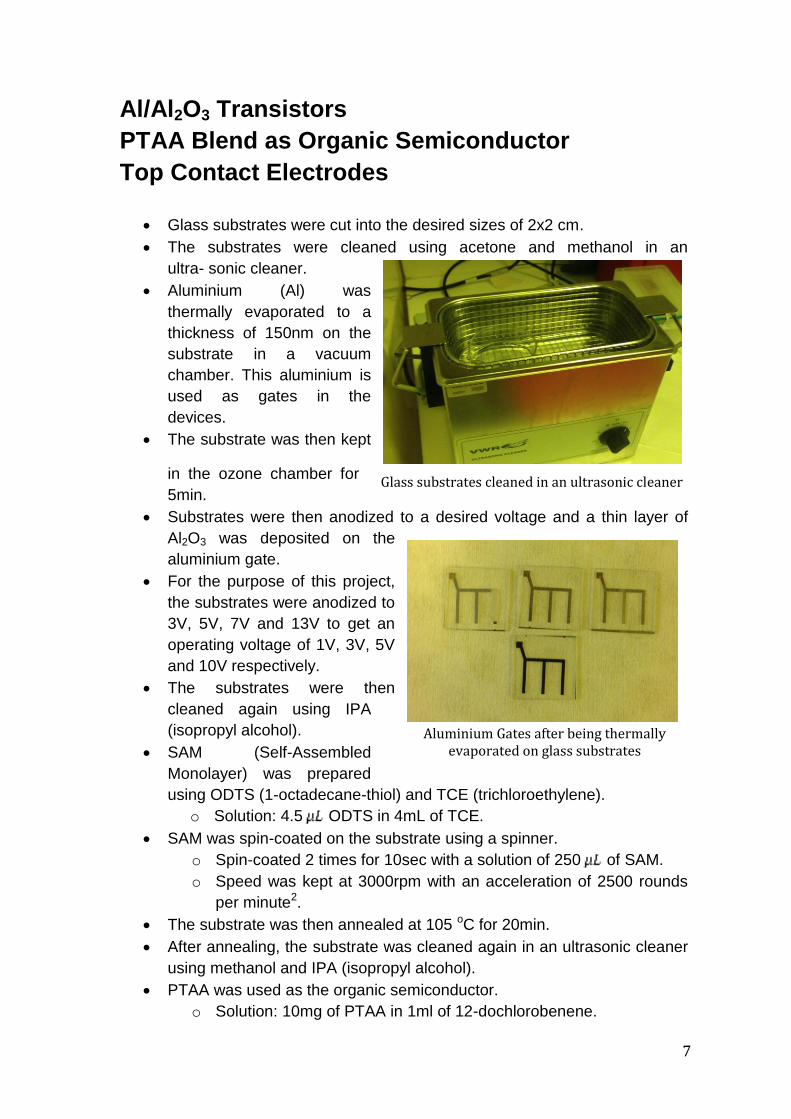
Aluminium (Al) was
thermally evaporated to a
thickness of 150nm on the
substrate in a vacuum
chamber. This aluminium is
used as gates in the
devices.
The substrate was then kept
in the ozone chamber for
5min.
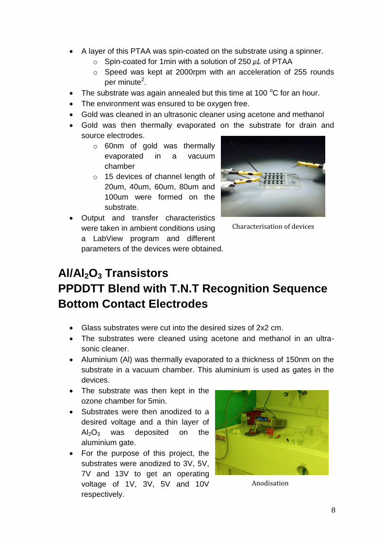
Substrates were then anodized to a desired voltage and a thin layer of
Al2O3 was deposited on the
aluminium gate.
For the purpose of this project,
the substrates were anodized to
3V, 5V, 7V and 13V to get an
operating voltage of 1V, 3V, 5V
and 10V respectively.
The substrates were then
cleaned again using IPA
(isopropyl alcohol).
SAM (Self-Assembled
Monolayer) was prepared
using ODTS (1-octadecane-thiol) and TCE (trichloroethylene).
o Solution: 4.5 ODTS in 4mL of TCE.
SAM was spin-coated on the substrate using a spinner.
o Spin-coated 2 times for 10sec with a solution of 250 of SAM.
o Speed was kept at 3000rpm with an acceleration of 2500 rounds
per minute2.
The substrate was then annealed at 105 oC for 20min.
After annealing, the substrate was cleaned again in an ultrasonic cleaner
using methanol and IPA (isopropyl alcohol).
PTAA was used as the organic semiconductor.
o Solution: 10mg of PTAA in 1ml of 12-dochlorobenene.
Aluminium Gates after being thermally evaporated on glass substrates
Glass substrates cleaned in an ultrasonic cleaner
8
A layer of this PTAA was spin-coated on the substrate using a spinner.
o Spin-coated for 1min with a solution of 250 of PTAA
o Speed was kept at 2000rpm with an acceleration of 255 rounds
per minute2.
The substrate was again annealed but this time at 100 oC for an hour.
The environment was ensured to be oxygen free.
Gold was cleaned in an ultrasonic cleaner using acetone and methanol
Gold was then thermally evaporated on the substrate for drain and
source electrodes.
o 60nm of gold was thermally
evaporated in a vacuum
chamber
o 15 devices of channel length of
20um, 40um, 60um, 80um and
100um were formed on the
substrate.
Output and transfer characteristics
were taken in ambient conditions using
a LabView program and different
parameters of the devices were obtained.
Al/Al2O3 Transistors
PPDDTT Blend with T.N.T Recognition Sequence
Bottom Contact Electrodes
Glass substrates were cut into the desired sizes of 2x2 cm.
The substrates were cleaned using acetone and methanol in an ultra-
sonic cleaner.
Aluminium (Al) was thermally evaporated to a thickness of 150nm on the
substrate in a vacuum chamber. This aluminium is used as gates in the
devices.
The substrate was then kept in the
ozone chamber for 5min.
Substrates were then anodized to a
desired voltage and a thin layer of
Al2O3 was deposited on the
aluminium gate.
For the purpose of this project, the
substrates were anodized to 3V, 5V,
7V and 13V to get an operating
voltage of 1V, 3V, 5V and 10V
respectively.
Characterisation of devices
Anodisation
9
The substrates were then cleaned again using IPA (isopropyl alcohol).
Gold was cleaned in an ultrasonic cleaner using acetone and methanol
Gold and chromium were then evaporated on the substrate for drain and
source electrodes.
o 5nm of chromium and 55nm of gold were thermally evaporated in
a vacuum chamber.
o 15 devices of channel length of 20um, 40um, 60um, 80um and
100um were formed on the substrate.
2 layers of SAM are coated on the devices
The first layer of SAM (Self-Assembled Monolayer) was prepared using
ODTS (1-octadecane-thiol) and TCE (trichloroethylene).
o Solution: 4.5 ODTS in 4mL of TCE.
This solution was spin-coated on the substrate using a spinner.
o Spin-coated 2 times for 10sec with a solution of 250 of SAM.
o Speed was kept at 3000rpm with an acceleration of 2500 rounds
per minute2.
The second layer of SAM is prepared PFBT (Poly(fluorine-alt-
benzothiadiazole)) and IPA (isopropyl alcohol).
o Solution: 6.67 (10mM) in 5mL of IPA.
o 200 solution of PFBT is sprinkled on the devices and is rested
for 5min before cleaning it with IPA again.
The substrate was then annealed at 105 oC for 20min.
After annealing, the substrate was cleaned again in an ultrasonic cleaner
using methanol and IPA (isopropyl alcohol).
Solution of PPDDTT and T.N.T recognition sequence was used as the
organic semiconductor.
o Solution: (7:3 ratio of PPDDTT and T.N.T recognition sequence)
3.5mg of PPDDTT and 1.5mg of T.N.T in 1ml of 12-
dochlorobenene.
A layer of this solution was spin-coated on the substrate using a spinner.
o Spin-coated for 2min with a solution of 250 .
o Speed was kept at 2000rpm with an acceleration of 255 rounds
per minute2.
The substrate was again annealed but this time at 120 oC for 30min.
The environment was ensured to be oxygen free.
Output and transfer characteristics were taken in ambient conditions
using a LabView program and different parameters of the devices were
obtained.
10
Results
The Aim of this project was to understand the basic principle and working of an
Organic Field-Effect Transistor (OFETs). To gain a better understanding, many
different experiments and analysis were carried out during this project and many
results regarding OFETs were obtained. A compendium of these results have
been given below:
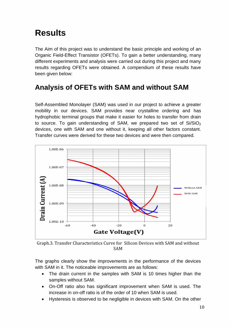
Analysis of OFETs with SAM and without SAM
Self-Assembled Monolayer (SAM) was used in our project to achieve a greater
mobility in our devices. SAM provides near crystalline ordering and has
hydrophobic terminal groups that make it easier for holes to transfer from drain
to source. To gain understanding of SAM, we prepared two set of Si/SiO2
devices, one with SAM and one without it, keeping all other factors constant.
Transfer curves were derived for these two devices and were then compared.
Graph.3. Transfer Characteristics Curve for Silicon Devices with SAM and without
SAM
The graphs clearly show the improvements in the performance of the devices
with SAM in it. The noticeable improvements are as follows:
The drain current in the samples with SAM is 10 times higher than the
samples without SAM.
On-Off ratio also has significant improvement when SAM is used. The
increase in on-off ratio is of the order of 10 when SAM is used.
Hysteresis is observed to be negligible in devices with SAM. On the other
11
hand, the devices without SAM have significant hysteresis.
Leakage current has also improved when SAM is used in devices.
On calculating the mobility, it was observed that devices with SAM had
mobility around 10-4cm2/V while the devices without SAM had mobility
around 10-5cm2/V. Hence mobility also increased by an order of 10 when
SAM was used in transistors.
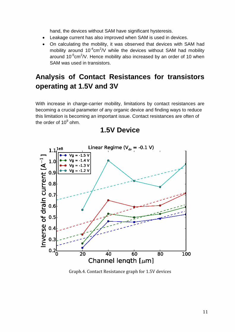
Analysis of Contact Resistances for transistors
operating at 1.5V and 3V
With increase in charge-carrier mobility, limitations by contact resistances are
becoming a crucial parameter of any organic device and finding ways to reduce
this limitation is becoming an important issue. Contact resistances are often of
the order of 109 ohm.
1.5V Device
Graph.4. Contact Resistance graph for 1.5V devices
12
Gate Voltage (V) Linear Contact
Resistance (Mohm)
Specific Linear Contact
Resistance (Mohm-cm)
-1.5 2.467 0.246
-1.4 2.895 0.289
-1.3 3.761 0.376
-1.2 6.572 0.657
Table.1. Contact Resistance table for 1.5V devices
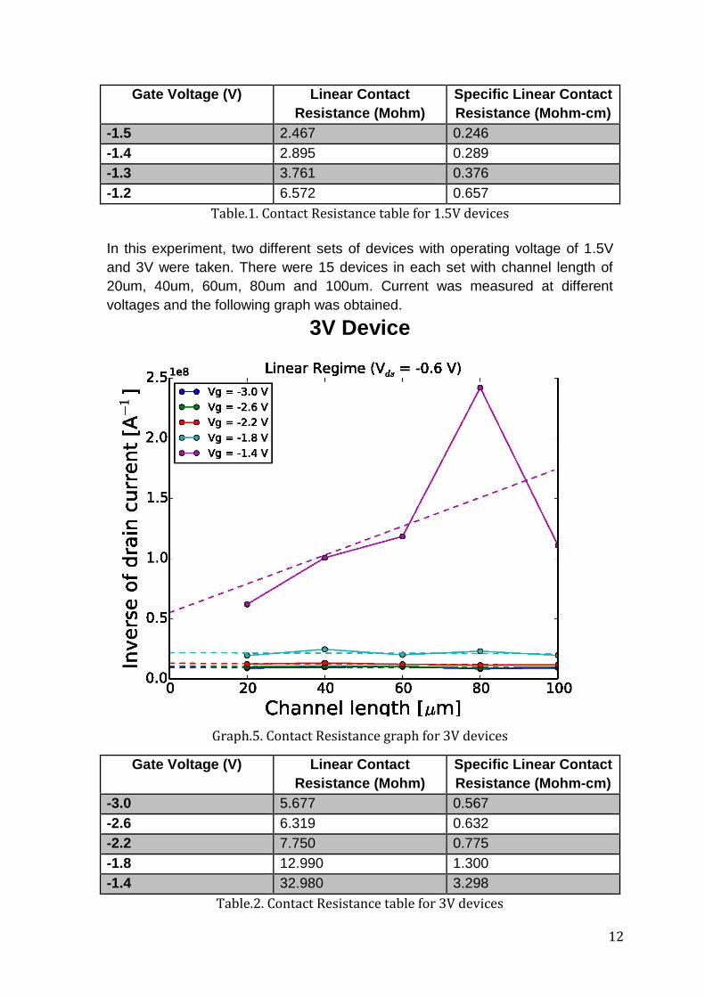
In this experiment, two different sets of devices with operating voltage of 1.5V
and 3V were taken. There were 15 devices in each set with channel length of
20um, 40um, 60um, 80um and 100um. Current was measured at different
voltages and the following graph was obtained.
3V Device
Graph.5. Contact Resistance graph for 3V devices
Gate Voltage (V) Linear Contact
Resistance (Mohm)
Specific Linear Contact
Resistance (Mohm-cm)
-3.0 5.677 0.567
-2.6 6.319 0.632
-2.2 7.750 0.775
-1.8 12.990 1.300
-1.4 32.980 3.298
Table.2. Contact Resistance table for 3V devices
13
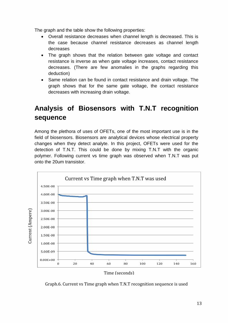
The graph and the table show the following properties:
Overall resistance decreases when channel length is decreased. This is
the case because channel resistance decreases as channel length
decreases
The graph shows that the relation between gate voltage and contact
resistance is inverse as when gate voltage increases, contact resistance
decreases. (There are few anomalies in the graphs regarding this
deduction)
Same relation can be found in contact resistance and drain voltage. The
graph shows that for the same gate voltage, the contact resistance
decreases with increasing drain voltage.
Analysis of Biosensors with T.N.T recognition
sequence
Among the plethora of uses of OFETs, one of the most important use is in the
field of biosensors. Biosensors are analytical devices whose electrical property
changes when they detect analyte. In this project, OFETs were used for the
detection of T.N.T. This could be done by mixing T.N.T with the organic
polymer. Following current vs time graph was observed when T.N.T was put
onto the 20um transistor.
Graph.6. Current vs Time graph when T.N.T recognition sequence is used
Current vs Time graph when T.N.T was used
Time (seconds)
Cu
rren
t (A
mp
ere)
14
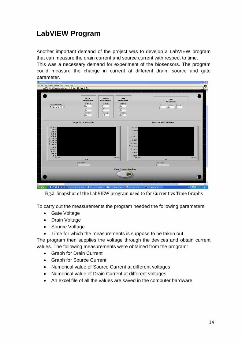
LabVIEW Program
Another important demand of the project was to develop a LabVIEW program
that can measure the drain current and source current with respect to time.
This was a necessary demand for experiment of the biosensors. The program
could measure the change in current at different drain, source and gate
parameter.
Fig.2. Snapshot of the LabVIEW program used to for Current vs Time Graphs
To carry out the measurements the program needed the following parameters:
Gate Voltage
Drain Voltage
Source Voltage
Time for which the measurements is suppose to be taken out
The program then supplies the voltage through the devices and obtain current
values. The following measurements were obtained from the program:
Graph for Drain Current
Graph for Source Current
Numerical value of Source Current at different voltages
Numerical value of Drain Current at different voltages
An excel file of all the values are saved in the computer hardware
15
Conclusion
Organic transistors have been in talks for the last few decades but only recently
have their been considered to be used industrially. Low cost, easy production
and mechanical flexibility are few of the many advantages that have lead to
extensive research in this field in the past few years. In this project, I gained not
only a basic understanding of the working of an organic transistor but also
carried out experiment to achieve the best working transistor. First part of the
project was to gain knowledge about the field by reading research papers and
articles. This helped to gain a firm grip on the basics of how the idea was
thought of and how has it started to become viable in the present world. After
doing thorough research I started conducting experiments to achieve the best
working transistor by experimenting with SAM and organic semiconductors. The
next part of the project was to carry out research on contact resistances and
what role do they play in working of an OFET. I also got the opportunity to work
on how OFETs are used as biosensors and how they can be used as an
engineering solution. Working with Dr. Majewski has helped me to gain valuable
knowledge about this upcoming field and also helped me broaden my horizon
about many different fields that are connected to nanostructures and
microelectronics.
Future Work
Working on this project helped conduct many experiments and analyze many
different ways in which OFETs can be used or improved. However, delving
deeper into this field made me realize how broad this subject is and how much
research is being carried out everyday. I would like to state few of the worked
that I would like to do in the future if I get another opportunity to work in this
field.
Working with some new organic polymers and getting the highest mobility
Doing some more research in the field of contact resistance and able to
get some conclusive results about how contact resistance can be
decreased.
Work with plastic substrates and achieve conclusive results with this
substrate.
References 1. Horowitz G. (1998). Organic Field-Effect Transistors. Advanced Materials. 10
(5), p365-377.
2. Jaiswal M and Menon R. (2006). Polymer electronic materials: a review of
charge transport. Society of Chemical Industry. 55, p1371-1384.
3. Burghard M, Klauk H and Kern K. (2009). Carbon-Based Field-Effect
Transistors for Nanoelectronics. Advanced Materials. 21, p2586-2600.
16
4. Moliton A and Hiorns R. (2013). The origin and development of (plastic) organic
electronics. Society of Chemical Industry. 61, p337-341.
5. Sirringhaus H. (2014). Organic Field-Effect Transistors: The Path Beyond
Amorphous Silicon. Advanced Materials. 26, p1319-1334.