
Low-PowerEmbeddedDSPCore forCommunicationSystems · Low-PowerEmbeddedDSPCore...
16
EURASIP Journal on Applied Signal Processing 2003:13, 1355–1370 c 2003 Hindawi Publishing Corporation Low-Power Embedded DSP Core for Communication Systems Ya-Lan Tsao Department of Electrical Engineering, National Central University, 300 Jung-Da Road, Jung-Li City, Taoyuan 320, Taiwan Email: [email protected] Wei-Hao Chen Department of Electrical Engineering, National Central University, 300 Jung-Da Road, Jung-Li City, Taoyuan 320, Taiwan Email: [email protected] Ming Hsuan Tan Department of Electrical Engineering, National Central University, 300 Jung-Da Road, Jung-Li City, Taoyuan 320, Taiwan Email: [email protected] Maw-Ching Lin Department of Electrical Engineering, National Central University, 300 Jung-Da Road, Jung-Li City, Taoyuan 320, Taiwan Email: [email protected] Shyh-Jye Jou Department of Electrical Engineering, National Central University, 300 Jung-Da Road, Jung-Li City, Taoyuan 320, Taiwan Email: [email protected] Received 2 February 2003 and in revised form 14 July 2003 This paper proposes a parameterized digital signal processor (DSP) core for an embedded digital signal processing system designed to achieve demodulation/synchronization with better performance and flexibility. The features of this DSP core include parame- terized data path, dual MAC unit, subword MAC, and optional function-specific blocks for accelerating communication system modulation operations. This DSP core also has a low-power structure, which includes the gray-code addressing mode, pipeline sharing, and advanced hardware looping. Users can select the parameters and special functional blocks based on the character of their applications and then generating a DSP core. The DSP core has been implemented via a cell-based design method using a synthesizable Verilog code with TSMC 0.35 µm SPQM and 0.25 µm 1P5M library. The equivalent gate count of the core area without memory is approximately 50 k. Moreover, the maximum operating frequency of a 16 × 16 version is 100 MHz (0.35 µm) and 140 MHz (0.25 µm). Keywords and phrases: digital signal processor, embedded system, dual MAC, subword multiplier. 1. INTRODUCTION During the past few years, digital signal processor (DSP) has become the fastest growing segment in the processor indus- try [1]. Today, almost all wireless handsets and base stations are DSP-based systems. Not only technological trends make DSP cheaper and more powerful, but DSP-based systems are also more cost effective and have shorter time to market than other systems [2]. Some DSPs can achieve high throughput by exploiting parallelism with specialized data paths at moderate clock fre- quency. For example, very long instruction word (VLIW) and single instruction multiple data (SIMD) approaches can be used to further enhance processor performance [3]. However, these approaches are not economical for dedi- cated application in area and power terms. Consequently, these structures are not suitable for embedded commu- nication applications, in which small area and low-power consumption are critical factors. Instead, an application- specific concept is used while maintaining a focus on the targeted application of the processor. Accordingly, the DSP architecture and bus structure have been set to optimize
-
Upload
trinhkhuong -
Category
Documents
-
view
214 -
download
0
Transcript of Low-PowerEmbeddedDSPCore forCommunicationSystems · Low-PowerEmbeddedDSPCore...

EURASIP Journal on Applied Signal Processing 2003:13, 1355–1370c© 2003 Hindawi Publishing Corporation
Low-Power Embedded DSP Corefor Communication Systems
Ya-Lan TsaoDepartment of Electrical Engineering, National Central University, 300 Jung-Da Road, Jung-Li City, Taoyuan 320, TaiwanEmail: [email protected]
Wei-Hao ChenDepartment of Electrical Engineering, National Central University, 300 Jung-Da Road, Jung-Li City, Taoyuan 320, TaiwanEmail: [email protected]
Ming Hsuan TanDepartment of Electrical Engineering, National Central University, 300 Jung-Da Road, Jung-Li City, Taoyuan 320, TaiwanEmail: [email protected]
Maw-Ching LinDepartment of Electrical Engineering, National Central University, 300 Jung-Da Road, Jung-Li City, Taoyuan 320, TaiwanEmail: [email protected]
Shyh-Jye JouDepartment of Electrical Engineering, National Central University, 300 Jung-Da Road, Jung-Li City, Taoyuan 320, TaiwanEmail: [email protected]
Received 2 February 2003 and in revised form 14 July 2003
This paper proposes a parameterized digital signal processor (DSP) core for an embedded digital signal processing system designedto achieve demodulation/synchronization with better performance and flexibility. The features of this DSP core include parame-terized data path, dual MAC unit, subword MAC, and optional function-specific blocks for accelerating communication systemmodulation operations. This DSP core also has a low-power structure, which includes the gray-code addressing mode, pipelinesharing, and advanced hardware looping. Users can select the parameters and special functional blocks based on the characterof their applications and then generating a DSP core. The DSP core has been implemented via a cell-based design method usinga synthesizable Verilog code with TSMC 0.35 µm SPQM and 0.25 µm 1P5M library. The equivalent gate count of the core areawithout memory is approximately 50 k. Moreover, the maximum operating frequency of a 16 × 16 version is 100MHz (0.35 µm)and 140MHz (0.25 µm).
Keywords and phrases: digital signal processor, embedded system, dual MAC, subword multiplier.
1. INTRODUCTION
During the past few years, digital signal processor (DSP) hasbecome the fastest growing segment in the processor indus-try [1]. Today, almost all wireless handsets and base stationsare DSP-based systems. Not only technological trends makeDSP cheaper and more powerful, but DSP-based systems arealso more cost effective and have shorter time to market thanother systems [2].
Some DSPs can achieve high throughput by exploitingparallelism with specialized data paths at moderate clock fre-
quency. For example, very long instruction word (VLIW)and single instruction multiple data (SIMD) approachescan be used to further enhance processor performance [3].However, these approaches are not economical for dedi-cated application in area and power terms. Consequently,these structures are not suitable for embedded commu-nication applications, in which small area and low-powerconsumption are critical factors. Instead, an application-specific concept is used while maintaining a focus on thetargeted application of the processor. Accordingly, the DSParchitecture and bus structure have been set to optimize

1356 EURASIP Journal on Applied Signal Processing
Cablechannel
RF/IFdownconverter
VGA &BPF
ADC Demodulator BlindFSE
DAGC
VCXO DACTR loopfilter
NCOCR loopfilter
CR PD
TRPD
Slicer
DFE
Figure 1: Typical block diagram of the demodulation and synchronization in the receiver of communication system.
the performance of DSP processors for the target applica-tions. Some special function blocks also influence the per-formance of application-specific DSPs. Notably, special func-tional blocks such as square-distance-and-accumulate forvector quantization, add-compare-select for the Viterbi al-gorithm, and the Galois field operation for forward error-control coding are provided in certain DSPs for basebandoperations [4, 5, 6, 7, 8]. For example, Lucent’s DSP 1618performs Viterbi decoding using a coprocessor, which sup-ports various decoding modes with control registers [5]. Aspecial function, called the mobile communication acceler-ator (MCA), is incorporated into the design of MDSP-II toaccelerate the complex MAC operation [8].
Consequently, combining a dedicated, high performanceDSP core with some special functional blocks to produce ahighly integrated system is a current trend [9, 10, 11, 12]. Theproposed design is parameterized and configurable and thuscan meet system requirements easily. The proposed DSP corecontains special blocks such as Hamming distance unit, sub-word multiplier, dual MAC unit, rounded/saturation mode,fixed-coefficient FIR filter, and slicer unit. The proposed DSPcore is designed to support the calculations in the demod-ulation/synchronization part of the receiver. Figure 1 illus-trates the typical block diagram of the demodulation andsynchronization in the receiver. Thus, this DSP core sup-ports operations such as scaling, digital FIR filtering (bothfixed-coefficient filter for pulse shaping and adaptive filter forequalization), symbol slicing, looping, complex multiplica-tion, and so on.
In the aspect of low-power design, the memory accessoperation is clearly the most power-consuming action inDSPs. Various low-power techniques are also used in theDSP developed here, including gray-code addressing and ad-vanced hardware looping; pipeline sharing and low-powerdata-path design are used to reduce power consumption. Theremainder of this paper is organized as follows: Section 2presents the architecture of the proposed DSP. Section 3then shows the design of the parameterized architecture andthe special functional blocks. Next, Section 4 discusses somelow-power design techniques used in this DSP core. Sub-sequently, implementation and design results are demon-
strated in Section 5. Finally, Section 6 makes some conclu-sions.
2. ARCHITECTURE OF THE DSP CORE
Figure 2 illustrates the overall architecture of the proposedNCU DSP [9]. The NCU DSP is a fixed-point DSP core. Thegrey blocks in Figure 2 are the special functional blocks andare optional blocks that can be chosen by the user. The DSPprocessor core itself is parameterized with several indepen-dent parameters. Users can set the parameters so that theDSP core fits the applications.
2.1. Bus andmemory architecture
One of the characteristics of the DSP processor is that it canmove large amounts of data to or from memory rapidly andefficiently. DSP processor has this characteristic because itneeds to process numerous calculations simultaneously. Tak-ing FIR as an example, one tap operation must make threeaccesses to memory, namely, coefficient access, data access,and write-back data. If the memory bandwidth is not wideenough, an operation must be split into several subopera-tions before it can be completed. Consequently, memory ar-chitecture is an important determinant of processor perfor-mance.
Figure 3 illustrates the modified Harvard architectureused in our work. The modified architecture contains oneprogram-memory bank and one data-memory bank withseparate program and data bus. The program and data mem-ories are single-port and dual-port RAM, respectively. Thedual-port RAM indicates that the DSP processor simulta-neously can make two accesses to RAM. This arrangementprovides a maximum of one program access and two dataaccesses per instruction cycle to enhance memory access ca-pacity.
Most of the DSP processors include one or more dedi-cated data-address generation units (DAGU) for calculatingdata address. NCU DSP supports three addressing modes,namely, the indirect addressing, register direct addressing,and immediate addressing modes, as listed in Table 1. Theindirect addressing mode requires one additional register

Low-Power Embedded DSP Core for Communication Systems 1357
NCU DSP processor function block
Data address generationARAU0, ARAU1
AR0∼AR7Program address generationPC, RC, BRC, RSA, REA
Programmemory
Datamemory
Slicer
PAB
PB
CAB
CB
DABDBEAB
EB
T
MA MB
MW
Multiplier
Adder
S R
0
MC
R0R1R2R3R4R5R6R7
MUXFIR
DelayReg.
Multiplier
MF
ALU
S R
MG
Hammingdistance
MH
Barrelshifter
Basic function block
Optional special function block
Optional multifunction block
Figure 2: The block diagram of NCU DSP.
file, called the auxiliary register (ARx), for storing data-memory address. Moreover, DSP processors usually needto access data using special addressing methods in manyDSP algorithms. Hence, NCU DSP supports linear address-ing, circular addressing, and bit-reversed address in the in-direct addressing mode. The circular addressing mode canbe used to operate the FIR filter, and convolution andcorrelation algorithm, while the FFT algorithm uses bit-reversed addressing. These specialized functions not only re-duce the programming burden but also enhance the per-formance of DSP under conditions of smooth data access.This enhanced performance is why the indirect addressingmode is the most important addressing mode in the DSPcores.
Figure 4a shows the straightforward method for calculat-ing the bit-reversed addressing value. In Figure 4a, “A” rep-resents the current address pointer value and “Step” repre-sents the offset value, which is added to or subtracted fromthe current pointer value. The internal carry propagation isfrom MSB to LSB, differing from normal addition. Notably,
the bit-reversed address is calculated by adding or subtract-ing the step value from MSB to LSB (if the step is +1, theaddress value will be 0000, 1000, 0100, 1100, 0010, 1010, . . .).This circuit in Figure 4a uses a ripple adder to construct thereversed carry propagation from MSB to LSB. However, thecircuit has n full-adder (FA) delay time. This delay time ofripple adder makes the instruction decode (ID) stage becomethe critical path of DSP core. Figure 4b illustrates the newbit-reversed addressing generation architecture. In Figure 4b,“A” and “Step” are reordered by reversed connecting. Theripple adder is replaced by a parallel adder which has less de-lay time with respect to ripple adder. Finally, the output ofthe parallel adder is the reversed order of the bit-reversedvalue. The proposed new structure, Figure 4b, has smallerdelay time than that of Figure 4a.
2.2. I/O interface
Required transmission methods differ with data type. TheI/O interface of NCU DSP contains three categories, the di-rect data access (DMA) mode, the handshaking mode, and

1358 EURASIP Journal on Applied Signal Processing
Data pathAddress bus
Data bus
Datamemory
EB
EAB
DB
DAB
CB
CAB
PB
PABProgrammemory
PAGUDAGUI/O
Figure 3: The bus architecture of NCU DSP.
Table 1: Data addressing modes.
Type Operation Syntax Function Description
Indirect addressingmode
∗ARx Address = ARx ARx contains the data-memory address.
∗ARx± Address = ARxARx = ARx±
After access, the address in ARx is incrementedor decremented by 1.
∗ARx ± 0BAddress = ARxARx = B(ARx ± AR0)
After access, AR0 is added to or subtractedfrom ARx with reverse carry propagation.
∗ARx ± 0Address = ARxARx = ARx ± AR0
After access, AR0 is added to or subtractedfrom ARx.
∗ARx ± 0%Address = ARxARx = circ(ARx ± AR0)
After access, AR0 is added to or subtractedfrom ARx with circular addressing.
Register directaddressing mode
ADD R0, R1, R2 R2 = R0 + R1Access the content of register as operanddirectly.
Immediate addressingmode
LAR # 1000 h AR0 AR0 = 1000 hGive the destination register or memorya value directly.
the merge mode. The DMA mode is to transfer data directlyfrom the outside of the DSP to the data memory of the DSPcore. The DMA mode is provided for transferring these dataquickly and conveniently. Notably, the DMA mode transferbatch data. The transfer rate is the same with the clock in theDSP core. The handshaking mode is for real-time data butthe data rate is not regular. The handshaking signals are re-quired to perform the data transfer in this mode. The mergemode is to transfer data in regular clock rate which is slowerthan the internal clock of DSP core. In DMA mode, the DSP
core is halt until the data transfer is finished. The DSP core isrunning when data are transferred in merge mode and hand-shaking mode. Notably, the data transfer in the handshakingand merge modes occurs between the data outside the NCUDSP core and the host programmable interface (HPI) mem-ory. The HPI memory resembles a buffer of data memory.
2.3. Pipeline stage
The NCU-DSP contains six pipeline stages, namely, instruc-tion fetch (IF) stage, ID stage, operand fetch (OP) stage,

Low-Power Embedded DSP Core for Communication Systems 1359
Cn
Sn
AnStepn
FAnCn−1 · · · C3
A2
S2
Step2
FA2C2
A1Step1
FA1
S1
C1
A0Step0
FA0C0
S0
(a)
Sn−1 . . . S2 S1 S0
N-bit parallel adder
A0 A1 A2 . . . An−1 Step0 Step1 Step2 . . . Stepn−1
An−1 . . . A2 A1 A0 Stepn−1 . . . Step2 Step1 Step0
· · ·
· · ·· · ·
· · ·
· · ·
· · ·
(b)
Figure 4: (a) Previous and (b) new bit-reversed addressing generator architecture in NCU DSP.
Datapath2
Datapath1
Dual-portmemory
ARAU
Stack/memory/selection
Clk
Decoder2Decoder1
IF ID OP EX1 EX2 WB
Figure 5: The pipeline stages of NCU DSP.
execution one (EX1) stage, execution two (EX2) stage, andwrite-back (WB) stage, as shown in Figure 5. To acceleratethe performance of NCU-DSP, data-path calculation wassplit into the EX1 and EX2 stages. The most troublesomeproblems encountered using the pipelining technique weredata hazards [13]. Data hazards occur when the next in-struction needs to use data that is still being calculated bythe present instruction. Six clock cycles are required for thepresent instruction to calculate the data and write it backto memory. The next instruction fetches the data just threestages behind (OP stage). Consequently, the programmerneeds to insert some useless instructions (e.g., NOP) to avoidthe data hazard. To reduce the penalties arising from datahazards, this work adopts the data-forwarding technique in[13, 14].
The following example describes an example of data haz-ard:
· · · · · · · · ·STL A,∗AR3
MAC2 ∗AR3,∗AR2, A
· · · · · · · · ·
The ∗AR3 is not ready until “STL” completes in thesixth stage. Thus, three NOPs must be added between “STL”and “MAC2.” Figure 6 illustrates the data-forwarding tech-nique, which reduces the required number of NOPs to justone.

1360 EURASIP Journal on Applied Signal Processing
Read (AR3)
2. MAC2
1. STL
IF DE OP EX1 EX2 WB
IF DE OP EX1 EX2 WBWrite (AR3)
(a)
Read (AR3)
3. MAC2
2. NOP
1. STL
IF DE OP EX1 EX2 WB
IF DE OP EX1 EX2 WBWrite (AR3)
(b)
Figure 6: (a) An example of data hazard. (b) Using of data-forwarding technique to resolve the data hazard.
3. DATA PATH AND SPECIAL FUNCTIONAL BLOCKS
3.1. Dual MAC architecture
The MAC data-path operation, which is the most importantinstruction in DSP, is the key to enhancing DSP operationperformance. Millions of multiply accumulates per second(MMACS) is more relevant than millions of instructions persecond (MIPS). Here, “dual” indicates two MACs per cycle.For example, the FIR algorithm is the most apparent usage ofthe dual MAC unit. The following equation can express theoperation of the FIR filter process:
Y(n) =N−1∑
i=0h(i) · X(n− i), (1)
where Y(n) denotes the output sample, h(i) represents thecoefficient, and X(n − i) is the input data. Two consecutiveoutput samples can be listed for analysis:
Y(0) = h(0) · X(0) + h(1) · X(−1)+ h(2) · X(−2) + · · · + h(N − 1) · X(1−N),
Y(1) = h(0) · X(1) + h(1) · X(0)+ h(2) · X(−1) + · · · + h(N − 1) · X(2−N).
(2)
Each output sample of N taps filter will take N instruc-tion cycles in the single MAC path. To accelerate perfor-
Accumulatorregisters
NaccNacc
ALUACC
MPY2MPY1
Delayregister
NdataNdataNdata
YmemSmem
Figure 7: The dual MAC data-path block diagram.
mance, this work established another MAC path in the DSPdata path, as shown in Figure 7. This secondMAC path com-prises a newly added multiplier along with the original ALUblock. Regarding the data-flow consideration, a delay registeris added between the single MAC path and the second MACpath to create the data source. This approach can save dataaccess requests where the coefficient remains the same foreach arm (Table 2). This architecture can be used to obtaintwo output samples simultaneously. Therefore, only aroundN/2 instruction cycles are required to complete the same op-erations in the single MAC architecture. Meanwhile, the dualMAC unit also reduces memory access power consumption.The single MAC unit needs 2N memory accesses, while the

Low-Power Embedded DSP Core for Communication Systems 1361
Table 2: The performance comparison of MAC structures in FIR algorithm [15].
Single MAC Dual MAC with 3 access bus Dual MAC with Reg.
No. of MAC operation N N N
No. of memory read 2N 2N N
No. of instruction cycle N N/2 N/2
Table 3: The overhead of the special block.
Clock cycle(without special block) Process Overhead
Overhead∗
(percentage)
Hamming distance calculator (16 bits) 1(33)0.35 µm 174 (gate count) 0.35%0.25 µm 238 (gate count) 0.38%
Multilevel slicer (16 bits) 1(2N ;N = log(symbol level))0.35 µm 65 (gate count) 0.13%0.25 µm 175 (gate count) 0.28%
Subword MAC unit (16 bits) 1(4)0.35 µm 1 396 (gate count) 2.79%0.25 µm 1 669 (gate count) 2.70%
Dedicated FIR filter with N taps1(N at single MAC;
N/2 dual MAC)Depends on spec.of FIR filter
Advance hardware looping1(5) 0.35 µm 850 (gate count) 1.70%
1(5) 0.25 µm 988 (gate count) 1.60%
Dual MAC (additional multiplier) 1(2)0.35 µm 2 488 (gate count) 4.98%0.25 µm 1 337 (gate count) 2.17%
∗Area of whole DSP exclude memory in 0.35 µm is estimated as 49 895 gates and area in 0.25 µm process is estimated as 61 751 gates.
dual MAC unit only requires N memory accesses [15]. Thedual MAC architecture is an optional special function. In ourdual MAC architecture, the hardware overhead is only onedelay register and one multiplier (MPY2). The critical de-lay path of dual MAC structure is the same with the singleMAC architecture. The user can select the function as op-tional. Table 3 lists the overheads of additional multipliers indifferent technologies.
3.2. SubwordMAC
The subword process architecture can partition an n-bit datainto two n/2-bit data so that data processing can be accel-erated, as in the I/Q channel data processing of the com-munication system. Furthermore, in certain cases, parts ofthe system do not need to operate at high resolution, mean-ing data can be expressed using a half-word length. Based onthe half-word-length representation, a set of parallel subwordprocess paths can be designed rather than a full-word pro-cess path. Subword parallelism process is also highly efficientfor application-specific data processors [16, 17]. For exam-ple, the subword MAC unit can reduce the complex MACoperation [17]. The complex vector of operations includesreal and image parts. Multiplying complex numbers requiresfour multiplication operations. Notably, the subword MACunit achieved fourMACoperations in a single cycle. The sub-word process can be further divided into two parts, namely,the subword multiplier and the subword accumulator.
A subword multiplier is designed to complete three dif-ferent types of multiplications: subword multiplication, con-ventional full-word multiplication, and complex-word mul-tiplication, as illustrated in Figure 8. The first mode, namely,the subword mode, is designed to multiply the upper andlower half of operands, respectively. Moreover, the sec-ond mode, conventional full-word multiplication, is imple-mented to help the subword multiplier maintain the capa-bility to perform a full-word process. Finally, the third mode,complex-wordmultiplication, assumes that a full-word com-prises both real-part and image-part subwords.
This design assumes that both full-word and subworddata are coded in the two’s complement system. This workuses AH to indicate the upper half and AL to indicate thelower half of a word; “AH@AL” represents “AH× 2Nsub +AL,”where Nsub is the number of bits in a subword.
The multiplier mainly comprises four subword multipli-ers (with outputs of carry and summation words to avoidthe requirement of carry-propagation adder) followed by acarry-save-adder (CSA) tree, as shown in Figure 9. Each sub-word multiplier is designed as a booth multiplier, meaningthat it only deals with signed data. In the subword multi-plication mode, operands need to be sent to the multiplier,and then the corresponding results are selected from sub-word multipliers.
Regarding the second mode, the conventional full-wordmultiplication, the arrangement displayed in Figure 8b is

1362 EURASIP Journal on Applied Signal Processing
2×Ndata
AL× BLAH × BH
BH BLAH AL
Ndata
×
(a)
AH × BHAH × BL
AL× BHAL× BL
A× B
AHBH
ALBL×
+
(b)
Image partReal part
(AH × BH)− (AL× BL) (AL× BH) + (AH × BL)
−(AL× BL)AH × BH
AH × BLAL× BH
AHBH
ALBL×
+
(c)
Figure 8: (a) Subword multiplication in subword multiplier. (b)Full-word multiplication in subword multiplier. (c) Complex-wordmultiplication.
impractical, and thus a compensation term is required to cor-rect the computation results. This situation exists because theoperand A in the two’s complement number system cannotbe represented using AH@AL directly. The problem in full-word multiplication can be expressed as follows:
B = −BNdata−1 × 2Ndata−1 +Ndata−2∑
i=0Bi × 2i,
BH = −BNdata−1 × 2Ndata−1 +Ndata−2∑
i=Nsub
Bi × 2i,
BL = −BNsub−1 × 2Nsub−1 +Nsub−2∑
i=0Bi × 2i,
B = BH@BL + BNsub−1 × 2Nsub .
(3)
According to booth multiplier characteristic, the operand A
which acts as the multiplicand should be modified as
AH =Ndata−1∑
i=Nsub
Ai × 2i−Nsub+1 + ANsub−1 . (4)
Thus, A× B can be expressed as
A× B = A×(BH@BL + BNsub−1 × 2Nsub
)
= A× (BH@BL) + A× BNsub−1 × 2Nsub .(5)
The term A × BNsub−1 × 2Nsub is the compensation term thatshould be implemented. The subword multiplier developedhere can compensate this term in the CSA tree following themultipliers. Notably, the compensation term exists becausethe critical path presented here is located on the MAC path.The MAC function must be balanced between EX1 and EX2.The compensation term of the multiplier is left to the nextstage, EX2. Figure 9 also illustrates that the CSA tree is in theEX2 stage. Figure 10 shows the basic data arrangement in thecase of complex mode. A special arrangement occurs in thesubtraction in the real-part computation. The subtraction inthe two’s complement must perform the one’s complementof the subtraction first, and then add the complement andcompensation terms to the minuend. Similarly, the additionof the compensation term is implemented in the CSA tree.The word length of the subword MAC structure can be se-lected by the user and parameterized from 8 to 32 bits. Thesubword resolution ranges from 4 to 16 bits, respectively. In[17, 18] the MAC data path is accomplished in one pipelinestage. In our design, it is arranged across two pipeline stages.Each multiplier has two outputs to avoid carrying propaga-tion in the final stage of multiplier. The multiplier outputs,compensation term, and accumulation output are summedby CSA tree to speed up the computation. Moreover, in thefull-word multiplication mode, due to the compensation-term arrangement, we do not have to cascade twomultipliersoperation as those used in [18].
The subwordMAC and non-subwordMAC are both syn-thesized and evaluated. The area of 0.35 µm design (16× 16)is approximately 12132 gate counts (subword) and 10736gate counts (nonsubword). The delay times of both casesare synthesized to meet 5.56 nanoseconds. The overhead is1396 gate counts, approximately 13% compared to the non-subword MAC. In the 0.25 µm technology design, the sub-word and non-subword MAC were synthesized to meet the 5nanoseconds delay time. The area of subwordMAC (16×16)is about 8669 gate counts, while that of non-subwordMAC isaround 7000 gate counts. The overhead of the subwordMACis approximately 23.8% with respect to the non-subwordMAC. The subword MAC generally consumes 20% morepower than the non-subword MAC.
3.3. Optional special functional blocksand parameters
The special function blocks are merged into the NCU-DSPdescribed here for two important reasons. First, in some

Low-Power Embedded DSP Core for Communication Systems 1363
SEL
EX1 EX22
MultiplierAH × BH
Nsub
Nsub
MultiplierAH × BL
Nsub
Nsub
MultiplierAL× BH
Nsub
Nsub
MultiplierAL× BL
Nsub
Nsub
Ndata
Ndata
BA
Controllogic
CSAtree Accumulator
Figure 9: Subword multiplier architecture.
SubwordSignof AH
AHSignof AL
AL
FullwordSignof A
A
Figure 10: Subword data arrangement.
applications with high sampling rate, special functionalblocks represent the only reasonable approach. If the DSPprocessor can provide special data paths that comprise thesefunctional blocks and do not increase overheads significantly,then the provision of these paths is worthwhile. Second, com-munication systems usually use some special function unitswith a small area compared to the overall DSP gate counts.For example, the multilevel slicer unit can reduce the in-struction cycles of a symbol mapper operation in commu-nication system. It can reduce the symbol mapper opera-tion from 2N , N = log(symbol level), to just one instruc-tion cycle. The circuit area overheads of the functional blockare only 0.13% (0.35 µm) and 0.28% (0.25 µm) of the wholeDSP core (excluding memory). For reasons of performanceand flexibility, these blocks are alsomerged in our NCU-DSP.Based on the above two reasons, some special function cir-cuits are offered for selection, as listed in Table 4. Table 3 liststhe hardware overheads and acceleration factors of these cir-cuits.
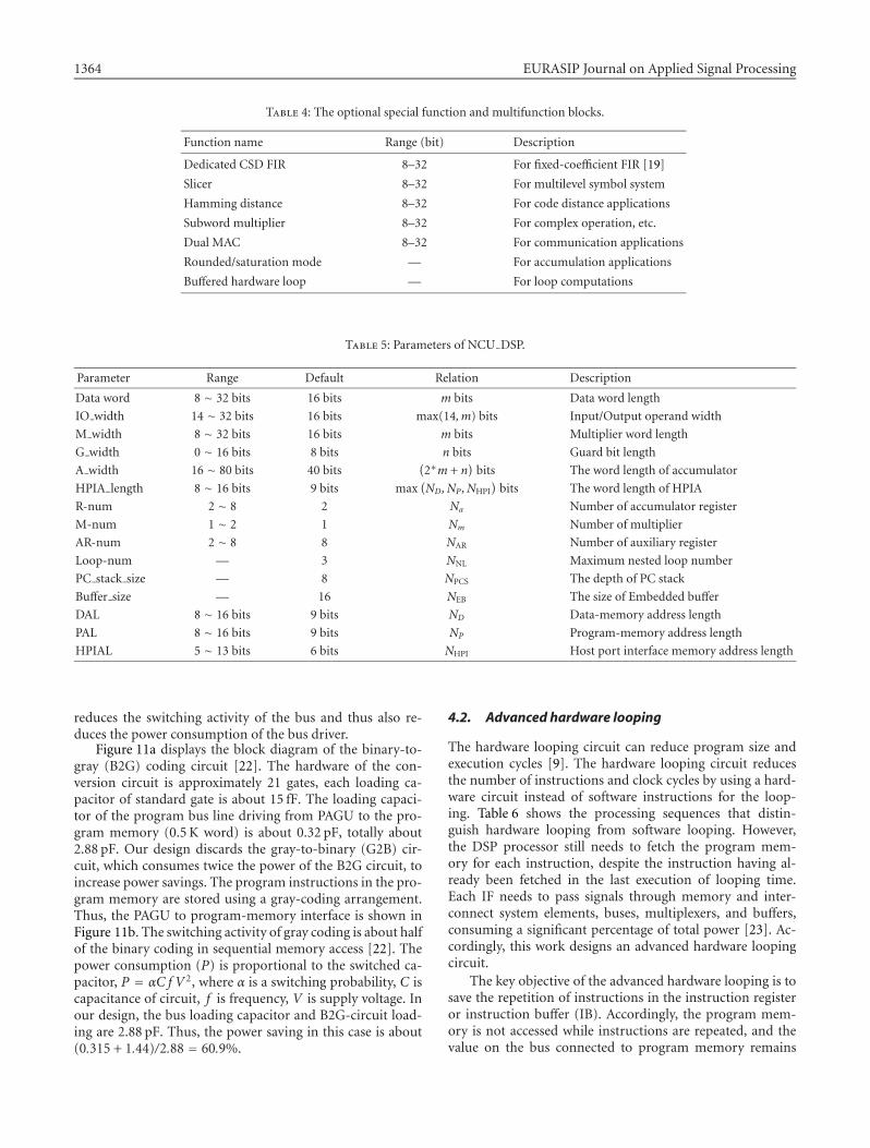
Recently, a more flexible DSP core has been proposed,namely, the so-called parameterized DSP core [20]. The pa-rameterized DSP core is parameterized using several inde-pendent parameters. Table 5 lists the parameters of NCUDSP. The most important parameter in the table is the “dataword.” This parameter exerts the biggest influence on the
chip size and performance of the NCU-DSP. For users towhom chip area is important, care must be taken regardingthe parameters data address length (DAL) and program ad-dress length (PAL). Care is necessary because memory gen-erally occupies a large part of the total area of the DSP pro-cessor. Some parameters are related to one another. For ex-ample, ALU is used to calculate the operands from the multi-plier or accumulator. Consequently, the word length of ALUmust be related to the multiplier and accumulator. The re-lated functional blocks must have the same data length.
4. LOW-POWER DESIGN
Various methods of saving power have been proposed for usein the design of DSP. These methods include bus segmenta-tion, data access reduction, program memory access reduc-tion, gray-code addressing, and pipeline register reduction[21, 22]. The following sections address some key low-powerdesign methods used in the DSP presented here.
4.1. Gray-code addressing
The advantage of gray code compared to straight binarycode is that gray code changes by only one bit while chang-ing from one number to the next number. That is, if thememory access pattern is a sequence of consecutive ad-dress, each memory access changes by only one bit at its ad-dress bits. Owing to instruction locality during program ex-ecution, the program memory accesses in DSP applicationsare mostly sequential. Therefore a significant number of bitswitching can be eliminated via gray-code addressing [21].For example, the sequence of number from 0 to 15 are 26bits switched when the number is encoded in binary repre-sentation, and are only 15 bits switched when the numberis encoded in gray-code representation. This arrangement
1364 EURASIP Journal on Applied Signal Processing
Table 4: The optional special function and multifunction blocks.
Function name Range (bit) Description
Dedicated CSD FIR 8–32 For fixed-coefficient FIR [19]
Slicer 8–32 For multilevel symbol system
Hamming distance 8–32 For code distance applications
Subword multiplier 8–32 For complex operation, etc.
Dual MAC 8–32 For communication applications
Rounded/saturation mode — For accumulation applications
Buffered hardware loop — For loop computations
Table 5: Parameters of NCU DSP.
Parameter Range Default Relation Description
Data word 8 ∼ 32 bits 16 bits m bits Data word length
IO width 14 ∼ 32 bits 16 bits max(14,m) bits Input/Output operand width
M width 8 ∼ 32 bits 16 bits m bits Multiplier word length
G width 0 ∼ 16 bits 8 bits n bits Guard bit length
A width 16 ∼ 80 bits 40 bits(2∗m + n
)bits The word length of accumulator
HPIA length 8 ∼ 16 bits 9 bits max(ND,NP,NHPI
)bits The word length of HPIA
R-num 2 ∼ 8 2 Na Number of accumulator register
M-num 1 ∼ 2 1 Nm Number of multiplier
AR-num 2 ∼ 8 8 NAR Number of auxiliary register
Loop-num — 3 NNL Maximum nested loop number
PC stack size — 8 NPCS The depth of PC stack
Buffer size — 16 NEB The size of Embedded buffer
DAL 8 ∼ 16 bits 9 bits ND Data-memory address length
PAL 8 ∼ 16 bits 9 bits NP Program-memory address length
HPIAL 5 ∼ 13 bits 6 bits NHPI Host port interface memory address length
reduces the switching activity of the bus and thus also re-duces the power consumption of the bus driver.
Figure 11a displays the block diagram of the binary-to-gray (B2G) coding circuit [22]. The hardware of the con-version circuit is approximately 21 gates, each loading ca-pacitor of standard gate is about 15 fF. The loading capaci-tor of the program bus line driving from PAGU to the pro-gram memory (0.5 K word) is about 0.32 pF, totally about2.88 pF. Our design discards the gray-to-binary (G2B) cir-cuit, which consumes twice the power of the B2G circuit, toincrease power savings. The program instructions in the pro-gram memory are stored using a gray-coding arrangement.Thus, the PAGU to program-memory interface is shown inFigure 11b. The switching activity of gray coding is about halfof the binary coding in sequential memory access [22]. Thepower consumption (P) is proportional to the switched ca-pacitor, P = αC f V 2, where α is a switching probability, C iscapacitance of circuit, f is frequency, V is supply voltage. Inour design, the bus loading capacitor and B2G-circuit load-ing are 2.88 pF. Thus, the power saving in this case is about(0.315 + 1.44)/2.88 = 60.9%.
4.2. Advanced hardware looping
The hardware looping circuit can reduce program size andexecution cycles [9]. The hardware looping circuit reducesthe number of instructions and clock cycles by using a hard-ware circuit instead of software instructions for the loop-ing. Table 6 shows the processing sequences that distin-guish hardware looping from software looping. However,the DSP processor still needs to fetch the program mem-ory for each instruction, despite the instruction having al-ready been fetched in the last execution of looping time.Each IF needs to pass signals through memory and inter-connect system elements, buses, multiplexers, and buffers,consuming a significant percentage of total power [23]. Ac-cordingly, this work designs an advanced hardware loopingcircuit.
The key objective of the advanced hardware looping is tosave the repetition of instructions in the instruction registeror instruction buffer (IB). Accordingly, the program mem-ory is not accessed while instructions are repeated, and thevalue on the bus connected to program memory remains

Low-Power Embedded DSP Core for Communication Systems 1365
MSB LSBGray code
gn gn−1 gn−2 · · · g2 g1 g0
· · ·
bn bn−1 bn−2 · · · b3 b2 b1 b0
MSB LSBBinary code
(a)
Program memory
Binary-to-gray-codeconverter
Gray-codeaddress
PAGU
(b)
Figure 11: (a) Binary code to gray-code conversion circuit. (b) The conversion circuit in PAGU.
Table 6: Implementation of 1024 times ADD with hardware looping and software looping.
Hardware looping Software looping
InstructionRPTZ Reg0,1023ADD ∗AR1+, ∗AR2+, ∗AR3+
STM 1023, AR0
ADD ∗AR1+, ∗AR2+, ∗AR3+
ADD 1, ∗AR4
CMPR CC, AR4
BC pmad, cond
No. of instructions 1024 + 1 = 1025 1024× 4 + 1 = 4097
sp HW = 0, tag[sp + 1] = 1
BRC = 0, sp = sp end, sp HW �= 0, tag[sp + 1] = 0
BRC = 0, sp = sp end,
ST2
PC = #end of loop
ST1
BRC = 0, sp = sp end,
sp HW = 0
ST
Buf en
PC �= #end of loop
Figure 12: The state diagram of hardware looping.
unchanged. This approach can reduce the power consump-tion of the program memory and related buses.
The operation of repeating a block of instructions withIB can be divided into three phases, as displayed in Figure 12.Phase ST0 means that the hardware looping is inactive, and
thus no instructions need to be repeated. Meanwhile, inphase ST1, the hardware looping is active and IB receives in-structions from the program memory. Simultaneously, theinstructions are stored in the IB. But when the circuit is inphase ST2, the program memory is switched off and IR ac-cesses instructions from IB until the content of block-repeatcounter (BRC) becomes zero. This scheme means that pro-gram memory only needs to be accessed once.
To implement nested loop, this work adds a loop stackto store the repeat-start address (RSA) register, repeat-endaddress (REA) register, and BRC of the current loop. Thiswork focuses on the nested loop with the form illustrated inFigure 13a, and creates a new instruction, RPTBX. In case ofother forms, nested loop still can be implemented using ex-tra instructions such as PUSHHW and POPHW, as shown inFigure 13b. Since some applications may be concerned withchip area rather than power consumption, the nested loopcircuit and IB are regarded as an optional module. Further-more, the size of IB is also parameterized. Users can select thesize of IB. The design in our DSP differs from the popularso-called IB in [24, 25, 26]. The key difference is that IB doesnot work if the instruction is not looping. Moreover, IB onlystores the instructions contained in the loop. Additionally,in our design the IB involves no hitting rate or instruction

1366 EURASIP Journal on Applied Signal Processing
· · ·#end loop1
· · ·#end loop2
· · ·#end loop3
· · ·RPTBX No loop3
STM#end loop3, REA· · ·RPTBX No loop2
STM#end loop2, REA· · ·RPTBX No loop1STM#end loop1, REA
(a)
· · ·#end loop1
· · ·POPHW
#end loop3
· · ·RPTB No loop3
STM#end loop3, REA
PUSHHW
· · ·POPHW
#end loop2
· · ·RPTB No loop2
STM#end loop2, REA
PUSHHW
· · ·RPTB No loop1
STM#end loop1, REA
(b)
Figure 13: Examples of nested loop. (a) Loop that can be coded using instruction RPTBX. (b) Loop that can be coded using instructionsRPTB, PUSHHW, and POPHW.
StackData
memory
Programmemory
ARregister
DatapathM
UX
IF
Decoder
Shared bus
ID OF EX1 EX2 WB
Figure 14: The block diagram of pipeline sharing.
cycle penalties. Furthermore, the structure has negligibleoverheads compared to hardware looping without IB in otherDSPs. The control circuit of this advanced hardware looping
is only 1.6% overhead compared with the whole DSP area. IBsize is a parameter that can be varied according to applicationdemands.

Low-Power Embedded DSP Core for Communication Systems 1367
Table 7: Instruction examples of pipeline sharing.
Instruction Operation Data No. of stages passed
CC Cond, #lk #lk −→ PC, PC + 1 −→ stack while Cond is true PC + 1 4
ADDM Xmem, YmemORM Xmem, Ymem
Ymem = (Xmem) + (Ymem)Ymem = (Xmem)|(Ymem)
[ARx] 4
STH src, SHIFT, YmemSTL src, SHIFT, Ymem Ymem = src� SHIFT [ARx] 4
Table 8: Example of assembly code for a 16-tap FIR filter.
Address Instruction Comment
/∗∗∗∗∗∗∗∗& program data start∗∗∗∗∗∗∗∗∗∗∗∗/
0 LAR # 180 h, AR6 ;input buffer
1 LAR # 1 h, AR0 ;index
2 LAR # 4 fh, AR1 ;data pointer
3 LAR # 80 h, AR2 ;coefficient pointer
4 LAR # 100 h, AR7 ;output buffer
/∗∗∗∗∗∗∗∗∗FIR task∗∗∗∗∗∗∗∗∗/
5 STM # FIR filter loop, REA ;repeat block last position
6 STM # 17, BK1 ;for buffer size
7 STM # 17, BK2 ;for buffer size
8 RPTB # 255 ;hardware looping
9 LD # AR6+,C
a LD # AR6+,D
b LD # AR6+,B
/∗∗∗∗∗∗∗∗∗FIR filter∗∗∗∗∗∗∗∗∗/
c STL C, ∗AR1+,%
d STL D, ∗AR1+,%
e RPTZ A, 17 ;data forwarding
f MAC//MAC ∗AR1+0%, ∗AR2+0%, A, B ;dual MAC instruction
10 STH A, ∗AR7+ ;AR7 is outbuffer
11 STL B, ∗AR7+ ;AR7 is outbuffer
/∗∗∗∗∗∗∗∗∗FIR filter loop∗∗∗∗∗∗∗∗∗/
4.3. Pipeline sharing
In pipeline architecture, the pipeline registers contribute sig-nificantly to area and power consumption. Some signals sim-ply pass through the pipeline stages without being used.Therefore, the pipeline sharing technique was adopted hereto reduce the number of pipeline registers and thus reducepower and area.
Figure 14 shows the block diagram of pipeline sharing.Table 7 lists instructions that do not use the data address(ARi) and program address (PCi) until they are transmittedto the last pipeline stage. Therefore, these data occupy manyunnecessary pipeline registers. For example, the instructionADDM performs the addition of two memory operands andthen stores the result in the memory that holds the value ofARi until the final pipeline stage (WB). On the other hand,
the instruction CC, conditional call, maintains the value ofPCi plus one until the final stage. The values of PCi andARi share the same buses and pipeline registers. The multi-plexer determines which data are loaded into the shared bus.If some instructions do not use the shared bus and associatedpipeline registers, the value of buses and pipeline registerscan be held without passing through. The unpassing signalscontribute zero transition on the registers and buses to re-duce power consumption. The area overhead associated withthe pipeline sharing technique is a multiplexer and increasesthe complexity of the instruction decoder. In this parame-terized DSP, the size of the program and data memory maydiffer. Accordingly, the length of the shared bus should be themaximum of the address bus in terms of program and datamemory. The pipeline sharing method can be considered asa direct and simple way to save power consumption in the

1368 EURASIP Journal on Applied Signal Processing
Table 9: The design results.
Features NCU DSP NCU DSP
Technology TSMC 0.35 µm SPQM TSMC 0.25 µm 1P5M
Cell library Avant! 0.35 cell library Artisan 0.25 cell library
Power supply 3.3 V 2.5 V
Pipeline 6-stage 6-stage
Max. operating frequency 100MHz 140MHz
Die size 4 152 × 4 152 µm2 1 281 × 1 281 µm2 (estimated)
Core area (memory excluded) 51 349 gate counts 1 131 581 µm2 (65 485 gate counts)
On-chip memory512× 24 bit (program),512× 16 bit (data),64× 16 bit (HPI)
512× 24 bit (program), 16× 24 bit(Instruction buffer), 512× 16 bit (data),64× 16 bit (HPI)
Special function blocks Indirect addressing modeIndirect addressing mode subwordMultiplier Hamming distance slicer
data path circuit. The bus segment method performs well insaving power [27] which is dealing with data bus and addressbus. The example in [27] requires a more complicated con-trol circuit than pipeline sharing.
This pipeline sharing approach reduced four 16-bitpipeline registers and 64 wires out of eight 16-bit pipelineregisters and 128 wires in the example with a 16-bit wordstructure. The overhead associated with this approach in-clude a multiplexer and a slight increase in the complexityof the instruction decoder.
5. IMPLEMENTATION RESULTS AND EXAMPLE
5.1. FIR filter function example
Since the proposed dual MAC architecture, Figure 7, sup-ports two parallel operation of MAC, it can accelerate FIRoperation by a factor of two. Table 8 displays the example ofassembly code. The instructions #14∼#15 (address d and ad-dress e) in Table 8 are an example of data forwarding for twoNOP, saving. Significantly, the dual MAC structure requiresonly 18 instructions to complete the example. In contrast, ifonly oneMAC is used, it requires 35 instructions to completethe function.
5.2. Chip verification
To verify the NCU DSP, a 16-bit DSP core with an instruc-tion set of 24-bits word is designed. This architecture con-tains three memory blocks on chip, one 24-bit∗512-wordtwo-port RAM for the program memory, one 16-bit∗512-word dual-port SRAM for the data memory, and one 16-bits∗64-word dual-port SRAM for the HPI memory. Theword length of the accumulator is 40 bits, and the guardbits are relatively eight. The synthesis result demonstratesthat the maximum frequency is 140MHz with 0.25 µm cell-library implementation, and the critical path is the EX2 stage.Figure 15 displays the area of each stage with the 0.35 µm and0.25 µm cell library. Moreover, Figure 16 shows the timingcomparison of each stage with the 0.35 µm and 0.25 µm cell
IF ID IO EX1 EX2
Gatecounts
0
2000
4000
6000
8000
10000
12000
14000
7504 79337290
8670
2590
4291
6340
9190 8932
13521
0.35um
0.25um
Figure 15: The gate counts of each stage with 0.35 µm and 0.25 µmcell library.
library. Table 9 lists the features in the first (0.35 µm) and sec-ond (0.25 µm) versions of NCU DSP. This work uses the cell-based design flow to implement the DSP core. The 0.35 µmhas been taped out and the post-layout simulation revealsthat it operates effectively at 100MHz with 75mW. Figure 17shows the die photo of our design in 0.35 µm.
6. CONCLUSIONS
This work presented a parameterized embedded DSP corefor demodulation/synchronization in a communication sys-tem. The parameterized structure is easily embedded in sys-tems with different system requirements. The special func-tional blocks of this DSP core can achieve improved perfor-mance and flexibility with minimum area overhead. Further-more, NCU DSP is designed using several low-power meth-ods to reduce power consumption. The proposed DSP corecan meet the cost/performance in mostly DSP-based appli-cations.

Low-Power Embedded DSP Core for Communication Systems 1369
ns
0
1
2
3
4
5
6
7
8
9
EX2 EX1 IO ID IF
4.40
3.60
6.60
5.20
6.20
4.60
7.11
5.00
8.96
5.99
0.35um
0.25um
Figure 16: Timing comparison of each stage with 0.35 µm and0.25 µm cell library.
Programmemory
Datamemory
HPImemory
Figure 17: The die photo of NCU DSP (0.35 µm).
REFERENCES
[1] D. D. Clark, E. A. Feigenbaum, D. P. Greenberg, et al., “In-novation and obstacles: the future of computing,” IEEE Com-puter, vol. 31, no. 1, pp. 29–38, 1998.
[2] G. Frantz, “Digital signal processor trends,” IEEE Micro, vol.20, no. 6, pp. 52–59, 2000.
[3] J. Turley and H. Hakkarainen, “TI’s new ’C6x DSP screams at1600 MIPS,” Microprocessor Report, vol. 11, pp. 14–17, 1997.
[4] I. Verbauwhede andM. Touriguian, “A low power DSP enginefor wireless communications,” Journal of VLSI Signal Process-ing Systems, vol. 18, no. 2, pp. 177–186, 1998.
[5] AT&TData Sheet, DSP1618 digital signal processor, February1994.
[6] Texas Instruments, TMS320C54X DSP Reference Set, Volume1: CPU and Peripherals, 1997.
[7] M. Alidina, G. Burns, C. Holmqvist, E. Morgan, and
D. Rhodes, “DSP16000: A high performance, low power dual-MAC DSP core for communication applications,” in Proc.IEEE Custom Integrated Circuits Conference (CICC ’98), pp.119–122, Santa Clara, Calif, USA, May 1998.
[8] B. W. Kim, J. H. Yang, C. S. Hwang, et al., “MDSP-II: A 16-bitDSP with mobile communication accelerator,” IEEE Journalof Solid-State Circuits, vol. 34, no. 3, pp. 397–404, 1999.
[9] Y. Tsao, S. Jou, H. Lee, Y. Chen, and M. Tan, “An embeddedDSP core for wireless communication,” in Proc. InternationalSymposium on Circuit and System (ISCAS ’02), vol. 4, pp. 524–527, Scottsdale, Ariz, USA, May 2002.
[10] R. Mehra, L. M. Guerra, and J. M. Rabaey, “A partitioningscheme for optimizing interconnect power,” IEEE Journal ofSolid-State Circuits, vol. 32, no. 3, pp. 433–443, 1997.
[11] M. Kuulusa, J. Nurmi, J. Jakala, P. Ojala, and H. Herranen, “Aflexible DSP core for embedded systems,” IEEE Design & Testof Computers, vol. 14, no. 4, pp. 60–68, 1997.
[12] A. Gierlinger, R. Forsyth, and E. Ofner, “GEPARD: A param-eterisable DSP core for ASICS,” in Proc. International Confer-ence on Signal Processing Applications & Technology (ICSPAT’97), pp. 203–207, Scottsdale, Ariz, USA, 1997.
[13] D. A. Patterson and J. L. Hennessy, Computer Organization &Design: The Hardware/Software Interface, Morgan KaufmannPublishers, San Francisco, Calif, USA, 2nd edition, 1998.
[14] M. Sami, D. Sciuto, C. Silvano, V. Zaccaria, and R. Zafalom,“Exploiting data forwarding to reduce the power budget ofVLIW embedded processors,” in Proc. Conference and Exhibi-tion on Design, Automation and Test in Europe (DATE ’2001),pp. 252–257, Munich, Germany, March 2001.
[15] I. Verbauwhede and C. Nicol, “Low power DSP’s for wire-less communications,” in Proc. International Symposium onLow-Power Electronics and Design (ISLPED ’00), pp. 303–310,Rapallo, Italy, July 2000.
[16] J. Fridman, “Sub-word parallelism in digital signal process-ing,” IEEE Signal Processing Magazine, vol. 17, no. 2, pp. 27–35, 2000.
[17] Y. Huang and T. D. Chiueh, “A sub-word parallel digital signalprocessor for wireless communication systems,” in Proc. IEEEAsia-Pacific Conference on ASIC (AP-ASIC ’02), pp. 287–290,Taipei, Taiwan, August 2002.
[18] C. K. Chen, P. C. Tseng, Y. C. Chang, and L. G. Chen, “A digitalsignal processor with programmable correlator array archi-tecture for third generation wireless communication system,”IEEE Trans. on Circuits and Systems II: Analog and Digital Sig-nal Processing, vol. 48, no. 12, pp. 1110–1120, 2001.
[19] M. C. Lin, C. L. Chen, D. Y. Shin, C. H. Lin, and S. J.Jou, “Low-power multiplierless FIR filter synthesizer basedon CSD code,” in Proc. International Symposium on Circuitand System (ISCAS ’01), vol. 4, pp. 666–669, Sydney, Australia,May 2001.
[20] J. Nurmi and J. Takala, “A new generation of parameterizedand extensible DSP Cores,” in Proc. IEEE Workshop on SignalProcessing Systems: Design and Implementation (SiPS ’97), pp.320–329, Leicester, Midlands, UK, November 1997.
[21] C. L. Su, C. Y. Tsui, and A. M. Despain, “Low power architec-ture design and compilation techniques for high-performanceprocessors,” in Proc. IEEE International Computer Conference(COMPCON ’94), pp. 489–498, San Francisco, Calif, USA,February–March 1994.
[22] H. Mehta, R. M. Owens, andM. J. Irwin, “Some issues in graycode addressing,” in Proc. 6th Great Lakes Symposium on VLSI(GLS ’96), pp. 178–181, Des Moines, Iowa, USA, March 1996.
[23] P. Lapsley, J. Bier, A. Shoham, and E. A. Lee, DSP ProcessorFundamentals, IEEE Press, New York, NY, USA, 1997.
[24] C. Wu and T. T. Hwang, “Instruction buffering for nestedloops in low power design,” in Proc. International Symposium

1370 EURASIP Journal on Applied Signal Processing
on Circuit and System (ISCAS ’02), vol. 4, pp. 81–84, Scotts-dale, Ariz, USA, May 2002.
[25] M. Lewis and L. Brackenbury, “An instruction buffer for alow-power DSP,” in Proc. 6th International Symposium on Ad-vanced Research in Asynchronous Circuits and Systems (ASYNC’00), pp. 176–186, Eilat, Israel, April 2000.
[26] R. S. Bajwa, M. Hiraki, H. Kojima, et al., “Instruction buffer-ing to reduce power in processors for signal processing,” IEEETransactions on Very Large Scale Integration (VLSI) Systems,vol. 5, no. 4, pp. 417–424, 1997.
[27] J. Y. Chen, W. B. Jone, J. S. Wang, H.-I. Lu, and T. F. Chen,“Segmented bus design for low-power systems,” IEEE Trans-actions on Very Large Scale Integration (VLSI) Systems, vol. 7,no. 1, pp. 25–29, 1999.
Ya-Lan Tsao was born in Taiwan in 1967.He received his B.S. degree from the De-partment of Electrical Engineering, ChungCheng Institute of Technology in 1991 andM.S. degrees from the Department of Elec-tronics Engineering, National Central Uni-versity in 1996. He joined the Departmentof Electronic, Chung-Shan Institute of Sci-ence and Technology, Tao-Yuan, Taiwan in1991. Since 2000, he is a Ph.D. student inthe Department of Electronics Engineering, National Central Uni-versity. His research interests include high-speed, low-power digitalintegrated circuits design communication integrated circuits.
Wei-Hao Chen was born in Taiwan in 1977.He received his B.S. and M.S. degrees fromthe Department of Electronics Engineer-ing, National Central University in 2001and 2003. He joined VIA Technologies, Inc.,Taipei, Taiwan, right after his master course.His research interests include high-speed,low-power digital integrated circuits designand DSP system.
Ming Hsuan Tan was born in Taiwan in1975. He received his B.S. and M.S. de-grees from the Department of Electron-ics Engineering, National Central Univer-sity in 1999 and 2003. He joined VIA Tech-nologies, Inc., Taipei, Taiwan, right afterhis master course. His research interests in-clude high-speed, low-power digital inte-grated circuits design and DSP system.
Maw-Ching Lin was born in Taiwan in1962. He received his B.S. degree in elec-tronic engineering from Feng Chia Univer-sity, Tai Chung, in 1985 and M.S. degree inbiomedical engineering from Chung YuanChristian University, Chung Li, in 1994. Heis presently working toward the Ph.D. de-gree in electrical engineering at NationalCentral University, Chung Li. Since 1985, hehas been working at Chung Shan Instituteof Science and Technology, Lung Tan, Taiwan. Currently, he is anAssociate Scientist. His research interests include high-speed, low-power digital circuit design and architecture optimization in digitalsignal processing.
Shyh-Jye Jou was born in Taiwan in 1960.He received his B.S. degree in electrical en-gineering from National Chen-Kung Uni-versity in 1982, and M.S. and Ph.D. de-grees in electronics from National Chiao-Tung University in 1984 and 1988, respec-tively. He joined the Department of Electri-cal Engineering, National Central Univer-sity, Chung Li, Taiwan, in 1990 and is cur-rently a Professor. He was a Visiting Re-search Associate Professor in the Coordinated Science Laboratoryat the University of Illinois during 1993–1994 academic years. Heserved on the technical program committee of 1994–1996 CustomIntegrated Circuits Conference and was Technical ProgramCochairof the First, Second, and Third IEEE Asia Pacific Conference onASIC, 1999, 2000, and 2002. In the summer of 2001, he was a Vis-iting Research Consultant in the Communication Circuits & Sys-tems Research Laboratory of Agere Systems, USA. His research in-terests include high-speed, low-power digital integrated circuits de-sign, communication-integrated circuits, and simulation and anal-ysis tools for integrated circuits.