Low power JFET quad operational amplifier is information on a product in full production. January...
17
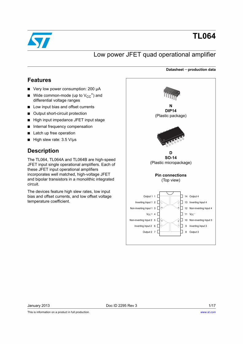
This is information on a product in full production. January 2013 Doc ID 2295 Rev 3 1/17 17 TL064 Low power JFET quad operational amplifier Datasheet − production data Features ■ Very low power consumption: 200 μA ■ Wide common-mode (up to V CC + ) and differential voltage ranges ■ Low input bias and offset currents ■ Output short-circuit protection ■ High input impedance JFET input stage ■ Internal frequency compensation ■ Latch up free operation ■ High slew rate: 3.5 V/μs Description The TL064, TL064A and TL064B are high-speed JFET input single operational amplifiers. Each of these JFET input operational amplifiers incorporates well matched, high-voltage JFET and bipolar transistors in a monolithic integrated circuit. The devices feature high slew rates, low input bias and offset currents, and low offset voltage temperature coefficient. N DIP14 (Plastic package) D SO-14 (Plastic micropackage) Pin connections (Top view) Inverting Input 2 Non-inverting Input 2 Non-inverting Input 1 CC V - CC V 1 2 3 4 8 5 6 7 9 10 11 12 13 14 + Output 3 Output 4 Non-inverting Input 4 Inverting Input 4 Non-inverting Input 3 Inverting Input 3 - + - + - + - + Output 1 Inverting Input 1 Output 2 www.st.com
Transcript of Low power JFET quad operational amplifier is information on a product in full production. January...
This is information on a product in full production.
January 2013 Doc ID 2295 Rev 3 1/17
17
TL064
Low power JFET quad operational amplifier
Datasheet − production data
Features
■ Very low power consumption: 200 µA
■ Wide common-mode (up to VCC+) and
differential voltage ranges
■ Low input bias and offset currents
■ Output short-circuit protection
■ High input impedance JFET input stage
■ Internal frequency compensation
■ Latch up free operation
■ High slew rate: 3.5 V/µs
Description
The TL064, TL064A and TL064B are high-speed JFET input single operational amplifiers. Each of these JFET input operational amplifiers incorporates well matched, high-voltage JFET and bipolar transistors in a monolithic integrated circuit.
The devices feature high slew rates, low input bias and offset currents, and low offset voltage temperature coefficient.
NDIP14
(Plastic package)
DSO-14
(Plastic micropackage)
Pin connections(Top view)
Inverting Input 2
Non-inverting Input 2
Non-inverting Input 1
CCV -CCV
1
2
3
4
8
5
6
7
9
10
11
12
13
14
+
Output 3
Output 4
Non-inverting Input 4
Inverting Input 4
Non-inverting Input 3
Inverting Input 3
-
+
-
+
-
+
-
+
Output 1
Inverting Input 1
Output 2
www.st.com

Contents TL064
2/17 Doc ID 2295 Rev 3
Contents
1 Schematic diagram . . . . . . . . . . . . . . . . . . . . . . . . . . . . . . . . . . . . . . . . . . 3
2 Absolute maximum ratings and operating conditions . . . . . . . . . . . . . 4
3 Electrical characteristics . . . . . . . . . . . . . . . . . . . . . . . . . . . . . . . . . . . . . 6
4 Parameter measurement information . . . . . . . . . . . . . . . . . . . . . . . . . . 11
5 Typical applications . . . . . . . . . . . . . . . . . . . . . . . . . . . . . . . . . . . . . . . . 11
6 ECOPACK® . . . . . . . . . . . . . . . . . . . . . . . . . . . . . . . . . . . . . . . . . . . . . . . . 12
6.1 DIP14 package mechanical data . . . . . . . . . . . . . . . . . . . . . . . . . . . . . . . 13
6.2 SO-14 package mechanical data . . . . . . . . . . . . . . . . . . . . . . . . . . . . . . . 14
7 Ordering information . . . . . . . . . . . . . . . . . . . . . . . . . . . . . . . . . . . . . . . 15
8 Revision history . . . . . . . . . . . . . . . . . . . . . . . . . . . . . . . . . . . . . . . . . . . 16
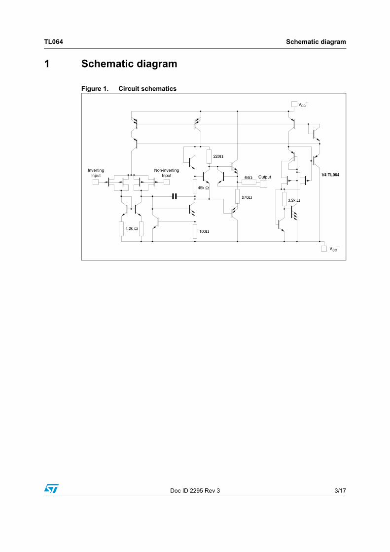
TL064 Schematic diagram
Doc ID 2295 Rev 3 3/17
1 Schematic diagram
Figure 1. Circuit schematics
Non-invertingInput
InvertingInput Output
VCC
1/4 TL064
4.2k Ω100Ω
45k Ω
220Ω
64Ω
270Ω3.2k Ω
VCC
Absolute maximum ratings and operating conditions TL064
4/17 Doc ID 2295 Rev 3
2 Absolute maximum ratings and operating conditions
Table 1. Absolute maximum ratings
Symbol Parameter Value Unit
VCC Supply voltage(1)
1. All voltage values, except differential voltage, are with respect to the zero reference level (ground) of the supply voltages where the zero reference level is the midpoint between VCC
+ and VCC-.
±18
VVi Input voltage(2)
2. The magnitude of the input voltage must never exceed the magnitude of the supply voltage or 15 volts, whichever is less.
±15
Vid Differential input voltage(3)
3. Differential voltages are the non-inverting input terminal with respect to the inverting input terminal.
±30
Ptot Power dissipation 680 mW
Rthja
Thermal resistance junction to ambient(4)(5)
DIP14 SO-14
4. Short-circuits can cause excessive heating and destructive dissipation.
5. Rth are typical values.
80105
°C/W
Rthjc
Thermal resistance junction to case(4)(5)
DIP14 SO-14
3331
Output short-circuit duration(6)
6. The output may be shorted to ground or to either supply. Temperature and/or supply voltages must be limited to ensure that the dissipation rating is not exceeded.
Infinite
Tstg Storage temperature range -65 to +150 °C
ESD
HBM: human body model(7)
7. Human body model: 100pF discharged through a 1.5kΩ resistor between two pins of the device, done for all couples of pin combinations with other pins floating.
900
VMM: machine model(8)
8. Machine model: a 200pF cap is charged to the specified voltage, then discharged directly between two pins of the device with no external series resistor (internal resistor < 5Ω), done for all couples of pin combinations with other pins floating.
200
CDM: charged device model(9)
9. Charged device model: all pins plus package are charged together to the specified voltage and then discharged directly to the ground.
1500
TL064 Absolute maximum ratings and operating conditions
Doc ID 2295 Rev 3 5/17
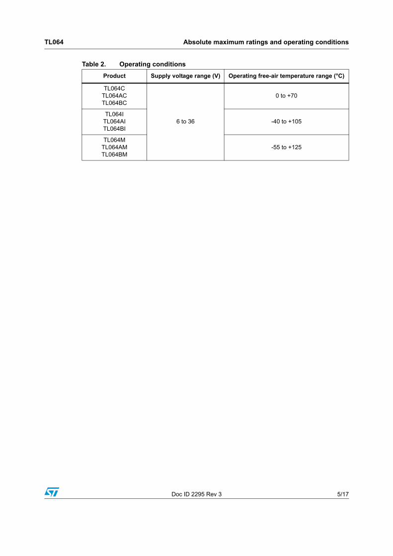
Table 2. Operating conditions
Product Supply voltage range (V) Operating free-air temperature range (°C)
TL064CTL064ACTL064BC
6 to 36
0 to +70
TL064ITL064AITL064BI
-40 to +105
TL064MTL064AMTL064BM
-55 to +125
Electrical characteristics TL064
6/17 Doc ID 2295 Rev 3
3 Electrical characteristics
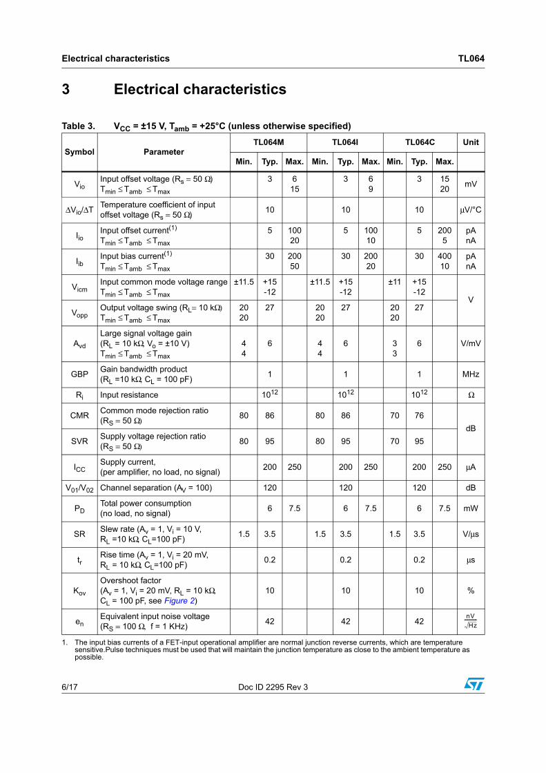
Table 3. VCC = ±15 V, Tamb = +25°C (unless otherwise specified)
Symbol ParameterTL064M TL064I TL064C Unit
Min. Typ. Max. Min. Typ. Max. Min. Typ. Max.
VioInput offset voltage (Rs = 50 Ω) Tmin ≤ Tamb ≤ Tmax
3 615
3 69
3 1520
mV
ΔVio/ΔTTemperature coefficient of input offset voltage (Rs = 50 Ω)
10 10 10 μV/°C
IioInput offset current(1) Tmin ≤ Tamb ≤ Tmax
5 10020
5 10010
5 2005
pAnA
IibInput bias current(1) Tmin ≤ Tamb ≤ Tmax
30 20050
30 20020
30 40010
pAnA
VicmInput common mode voltage range Tmin ≤ Tamb ≤ Tmax
±11.5 +15-12
±11.5 +15-12
±11 +15-12
V
VoppOutput voltage swing (RL= 10 kΩ) Tmin ≤ Tamb ≤ Tmax
2020
27 2020
27 2020
27
Avd
Large signal voltage gain (RL = 10 kΩ, Vo = ±10 V) Tmin ≤ Tamb ≤ Tmax
44
6 44
6 33
6 V/mV
GBPGain bandwidth product (RL =10 kΩ, CL = 100 pF)
1 1 1 MHz
Ri Input resistance 1012 1012 1012 Ω
CMRCommon mode rejection ratio (RS = 50 Ω) 80 86 80 86 70 76
dB
SVRSupply voltage rejection ratio (RS = 50 Ω) 80 95 80 95 70 95
ICCSupply current, (per amplifier, no load, no signal)
200 250 200 250 200 250 μA
V01/V02 Channel separation (AV = 100) 120 120 120 dB
PDTotal power consumption (no load, no signal)
6 7.5 6 7.5 6 7.5 mW
SRSlew rate (Av = 1, Vi = 10 V, RL =10 kΩ, CL=100 pF)
1.5 3.5 1.5 3.5 1.5 3.5 V/μs
trRise time (Av = 1, Vi = 20 mV, RL = 10 kΩ, CL=100 pF)
0.2 0.2 0.2 μs
Kov
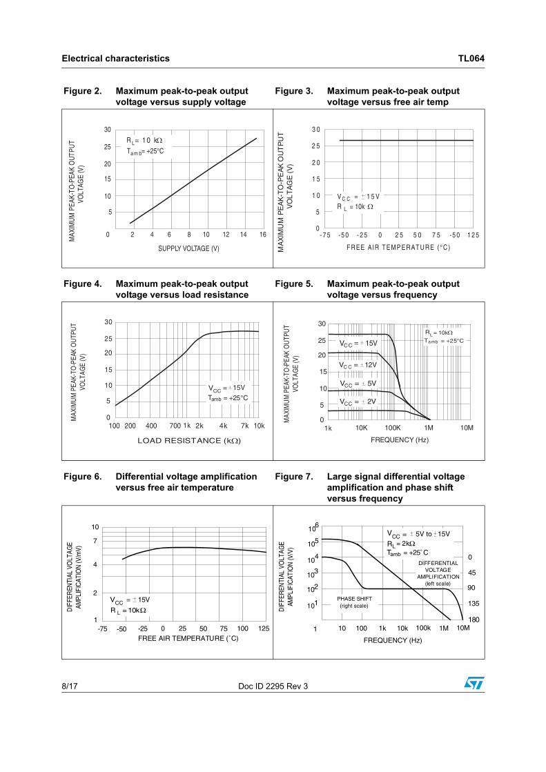
Overshoot factor (Av = 1, Vi = 20 mV, RL = 10 kΩ, CL = 100 pF, see Figure 2)
10 10 10 %
enEquivalent input noise voltage (RS = 100 Ω, f = 1 KHz)
42 42 42
1. The input bias currents of a FET-input operational amplifier are normal junction reverse currents, which are temperature sensitive.Pulse techniques must be used that will maintain the junction temperature as close to the ambient temperature as possible.
nV
Hz------------

TL064 Electrical characteristics
Doc ID 2295 Rev 3 7/17
Table 4. VCC = ±15 V, Tamb = +25°C (unless otherwise specified)
Symbol ParameterTL064AM, AI, AC TL064BM, BI, BC
UnitMin. Typ. Max. Min. Typ. Max.
VioInput offset voltage (Rs = 50 Ω) Tmin ≤ Tamb ≤ Tmax
3 67.5
2 35
mV
ΔVio/ΔTTemperature coefficient of input offset voltage (Rs = 50 Ω)
10 10 μV/°C
IioInput offset current(1) Tmin ≤ Tamb ≤ Tmax
5 1003
5 1003
pAnA
IibInput bias current(1) Tmin ≤ Tamb ≤ Tmax
30 2007
30 2007
pAnA
VicmInput common mode voltage range Tmin ≤ Tamb ≤ Tmax
±11.5 +15-12
±11.5 +15-12
V
VoppOutput voltage swing (RL = 10 kΩ) Tmin ≤ Tamb ≤ Tmax
2020
27 2020
27
Avd
Large signal voltage gain (RL = 10 kΩ, Vo = ±10 V) Tmin ≤ Tamb ≤ Tmax
44
6 44
6 V/mV
GBPGain bandwidth product (RL =10 kΩ, CL = 100 pF)
1 1 MHz
Ri Input resistance 1012 1012 Ω
CMR Common mode rejection ratio (RS = 50 Ω) 80 86 80 86 dB
SVR Supply voltage rejection ratio (RS = 50 Ω) 80 95 80 95 dB
ICCSupply current (per amplifier, no load, no signal)
200 250 200 250 μA
V01/V02 Channel separation (AV = 100) 120 120 dB
PDTotal power consumption (each amplifier, no load, no signal)
6 7.5 6 7.5 mW
SRSlew rate (Av = 1, Vi = 10 V, RL = 10 kΩ, CL = 100 pF)
1.5 3.5 1.5 3.5 V/μs
trRise time (Av = 1, Vi = 20 mV, RL = 10 kΩ, CL = 100 pF)
0.2 0.2 μs
KovOvershoot factor (Av = 1, Vi = 20 mV, RL = 10 kΩ, CL = 100 pF, see Figure 2)
10 10 %
enEquivalent input noise voltage (RS = 100 Ω, f = 1 KHz)
42 42
1. The input bias currents of an FET-input operational amplifier are normal junction reverse currents, which are temperature sensitive.Pulse techniques must be used that will maintain the junction temperature as close to the ambient temperature as possible.
nV
Hz------------
Electrical characteristics TL064
8/17 Doc ID 2295 Rev 3
Figure 2. Maximum peak-to-peak output voltage versus supply voltage
Figure 3. Maximum peak-to-peak output voltage versus free air temp
Figure 4. Maximum peak-to-peak output voltage versus load resistance
Figure 5. Maximum peak-to-peak output voltage versus frequency
Figure 6. Differential voltage amplification versus free air temperature
Figure 7. Large signal differential voltage amplification and phase shift versus frequency
10
2
4
7
DIF
FER
ENTI
AL V
OLT
AGE
AMPL
IFIC
ATIO
N (V
/mV)
-75 -50 -25 0 25 50 75 100 125FREE AIR TEMPERATURE (˚C)
V = 15VCCR = 10kΩL
110 100 1k 10k 100k 1M 10M
FREQUENCY (Hz)
610
510
410
310
210
110
1
DIF
FER
ENTI
AL V
OLT
AGE
AMPL
IFIC
ATIO
N (V
/V)
0
45
90
135
180
RL = 2kΩ= 5V to 15VVCC
= +25˚CTamb
DIFFERENTIAL VOLTAGE
AMPLIFICATION(left scale)
PHASE SHIFT(right scale)

TL064 Electrical characteristics
Doc ID 2295 Rev 3 9/17
Figure 8. Supply current per amplifier versus supply voltage
Figure 9. Supply current per amplifier versus free air temperature
TambNo signalNo load
= +25˚C
250
200
150
100
50
0
SUPP
LY C
UR
REN
T (μ
A)
0 2 64 8 10 12 14 16SUPPLY VOLTAGE ( V)
250
200
150
100
50
0
SUPP
LY C
UR
REN
T (μ
A)
-75 -50 0-25 25 50 75 100 125FREE AIR TEMPERATURE (˚C)
VCC = 15VNo signalNo load
Figure 10. Total power dissipated versus free air temperature
Figure 11. Common mode rejection ratio versus free air temperature
10
5
0
TOTA
L PO
WER
DIS
SIPA
TED
(mW
)
-50 -25 0 25 50 75 100 125
FREE AIR TEMPERATURE (˚C)
-75
15
20
25
30
= 15VVCCNo signalNo load
83
82
81
CO
MM
ON
MO
DE
REJ
ECTI
ON
RAT
IO(d
B)
-50 -25 0 25 50 75 100 125
FREE AIR TEMPERATURE (˚C)
-75
84
85
86
87
= 1 5VVC CR L = 10kΩ
Figure 12. Normalized unity gain bandwidth slew rate, and phase shift versus temperature
Figure 13. Input bias current versus free air temperature
0.9
0.8
0.7
NO
RM
ALIZ
ED U
NITY
-GAI
N B
AND
WID
THAN
D S
LEW
RAT
E
-50 -25 0 25 50 75 100 125
FREE AIR TEMPERATURE (˚C)
-75
1
1.1
1.2
1.3
UNITY-GAIN-BANDWIDTH(left scale)
PHASE SHIFT(right scale)
SLEW RATE(left scale)
= 15VVCCR L = 10kΩf = B for phase shift1
0.99
0.98
0.97
1
1.01
1.02
1.03 NO
RM
ALIZ
ED
PH
AS
E S
HIF
T
100
10
1
0.1
0.01
INPU
T BI
AS C
URR
ENT
(nA)
-50 -25 0 25 50 75 100 125
FREE AIR TEMPERATURE (˚C)
VCC = 15V

Electrical characteristics TL064
10/17 Doc ID 2295 Rev 3
Figure 14. Voltage follower large signal pulse response
Figure 15. Output voltage versus elapsed time
Figure 16. Equivalent input noise voltage versus frequency
6
4
2
0
-2
-4
0 2 4 6 8 10
INPU
T AN
D O
UTP
UT
VOLT
AGES
(V)
TIME (μs)
-6
OUTPUT
INPUT
= 15V= 10kΩRL
VCC
= 100pFCL
Tamb = +25̊ C
t r
28
24
20
16
12
8
4
0
-4
OU
TPU
T V
OLT
AG
E (m
V)
0 0.2 0.4 0.6 0.8 1 12 14
TIME ( μs)
10%
90%
OVERSHOOT
Tamb = +25˚C
VCC
= 15V
R L = 10k Ω
7060504030
20100
EQU
IVAL
ENT
INPU
T NO
ISE
VOLT
AGE
(nV/
VHz)
1040 100 400 1k 4k 10k 40k 100k
FREQUENCY (Hz)
8090
100
R S = 100ΩTa mb = +25˚C
VC C = 15V

TL064 Parameter measurement information
Doc ID 2295 Rev 3 11/17
4 Parameter measurement information
5 Typical applications
Figure 19. Audio distributor amplifier
Figure 17. Voltage follower Figure 18. Gain-of-10 inverting amplifier
-
-
e I
T L 0 6 4 e o
C L = 100pF R = 10k Ω L
1/4-eI
TL064
RL CL= 100pF
1k Ω
10k Ω
1/4eo
-
TL0641/4
-
-
-
TL0641/4
TL0641/4
TL0641/4
1M Ω
1μF
Output A
Output B
Output C
Input
100k Ω 100k Ω100k Ω
100k Ω1OO μF
V CC+
f = 100kHzO
ECOPACK® TL064
12/17 Doc ID 2295 Rev 3
6 ECOPACK®
In order to meet environmental requirements, ST offers these devices in different grades of ECOPACK® packages, depending on their level of environmental compliance. ECOPACK® specifications, grade definitions and product status are available at: www.st.com. ECOPACK® is an ST trademark.
TL064 ECOPACK®
Doc ID 2295 Rev 3 13/17
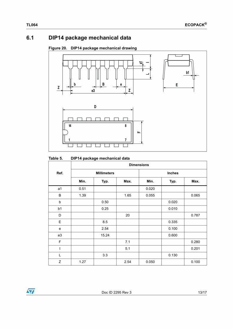
6.1 DIP14 package mechanical data
Figure 20. DIP14 package mechanical drawing
Table 5. DIP14 package mechanical data
Ref.
Dimensions
Millimeters Inches
Min. Typ. Max. Min. Typ. Max.
a1 0.51 0.020
B 1.39 1.65 0.055 0.065
b 0.50 0.020
b1 0.25 0.010
D 20 0.787
E 8.5 0.335
e 2.54 0.100
e3 15.24 0.600
F 7.1 0.280
I 5.1 0.201
L 3.3 0.130
Z 1.27 2.54 0.050 0.100
ECOPACK® TL064
14/17 Doc ID 2295 Rev 3
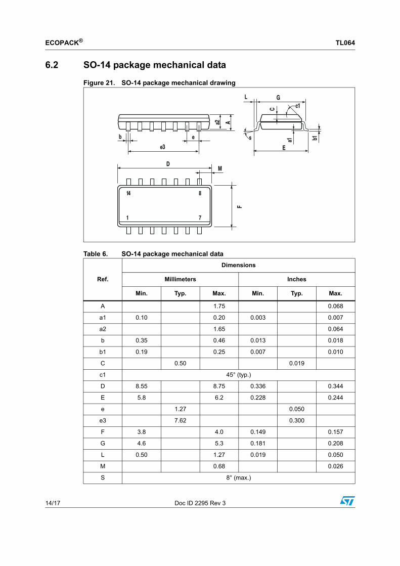
6.2 SO-14 package mechanical data
Figure 21. SO-14 package mechanical drawing
Table 6. SO-14 package mechanical data
Ref.
Dimensions
Millimeters Inches
Min. Typ. Max. Min. Typ. Max.
A 1.75 0.068
a1 0.10 0.20 0.003 0.007
a2 1.65 0.064
b 0.35 0.46 0.013 0.018
b1 0.19 0.25 0.007 0.010
C 0.50 0.019
c1 45° (typ.)
D 8.55 8.75 0.336 0.344
E 5.8 6.2 0.228 0.244
e 1.27 0.050
e3 7.62 0.300
F 3.8 4.0 0.149 0.157
G 4.6 5.3 0.181 0.208
L 0.50 1.27 0.019 0.050
M 0.68 0.026
S 8° (max.)

TL064 Ordering information
Doc ID 2295 Rev 3 15/17
7 Ordering information
064
Table 7. Order codes
Part numberTemperature
rangePackage Packing Marking
TL064MN
-55°C, +125°C
DIP14 Tube
TL064MN
TL064AMN TL064AMN
TL064BMN TL064BMN
TL064MD/DT
SO-14Tube or
tape & reel
064M
TL064AMD/DT 064AM
TL064BMD/DT 064BM
TL064IN
-40°C, +105°C
DIP14 Tube
TL064IN
TL064AIN TL064AIN
TL064BIN TL064BIN
TL064ID/DT
SO-14Tube or
tape & reel
064I
TL064AID/DT 064AI
TL064BID/DT 064BI
TL064CN
0°C, +70°C
DIP14 Tube
TL064CN
TL064ACN TL064ACN
TL064BCN TL064BCN
TL064CD/DT
SO-14Tube or
tape & reel
064C
TL064ACD/DT 064AC
TL064BCD/DT 064BC

Revision history TL064
16/17 Doc ID 2295 Rev 3
8 Revision history
Table 8. Document revision history
Date Revision Changes
13-Nov-2001 1 Initial release.
25-Jul-2007 2
Added Rthja, Rthjc and ESD values in Table 1: Absolute maximum ratings.
Added Table 2: Operating conditions.
Expanded Table 7: Order codes.
Format update.
09-Jan-2013 3
Updated Table 1: Absolute maximum ratings, Table 2: Operating conditions, Table 3: VCC = ±15 V, Tamb = +25°C (unless otherwise specified), Table 4: VCC = ±15 V, Tamb = +25°C (unless otherwise specified), and Table 7: Order codes.
Replaced Figure 17: Voltage follower.
TL064
Doc ID 2295 Rev 3 17/17
Please Read Carefully:
Information in this document is provided solely in connection with ST products. STMicroelectronics NV and its subsidiaries (“ST”) reserve the right to make changes, corrections, modifications or improvements, to this document, and the products and services described herein at any time, without notice.
All ST products are sold pursuant to ST’s terms and conditions of sale.
Purchasers are solely responsible for the choice, selection and use of the ST products and services described herein, and ST assumes no liability whatsoever relating to the choice, selection or use of the ST products and services described herein.
No license, express or implied, by estoppel or otherwise, to any intellectual property rights is granted under this document. If any part of this document refers to any third party products or services it shall not be deemed a license grant by ST for the use of such third party products or services, or any intellectual property contained therein or considered as a warranty covering the use in any manner whatsoever of such third party products or services or any intellectual property contained therein.
UNLESS OTHERWISE SET FORTH IN ST’S TERMS AND CONDITIONS OF SALE ST DISCLAIMS ANY EXPRESS OR IMPLIED WARRANTY WITH RESPECT TO THE USE AND/OR SALE OF ST PRODUCTS INCLUDING WITHOUT LIMITATION IMPLIED WARRANTIES OF MERCHANTABILITY, FITNESS FOR A PARTICULAR PURPOSE (AND THEIR EQUIVALENTS UNDER THE LAWS OF ANY JURISDICTION), OR INFRINGEMENT OF ANY PATENT, COPYRIGHT OR OTHER INTELLECTUAL PROPERTY RIGHT.
UNLESS EXPRESSLY APPROVED IN WRITING BY TWO AUTHORIZED ST REPRESENTATIVES, ST PRODUCTS ARE NOT RECOMMENDED, AUTHORIZED OR WARRANTED FOR USE IN MILITARY, AIR CRAFT, SPACE, LIFE SAVING, OR LIFE SUSTAINING APPLICATIONS, NOR IN PRODUCTS OR SYSTEMS WHERE FAILURE OR MALFUNCTION MAY RESULT IN PERSONAL INJURY, DEATH, OR SEVERE PROPERTY OR ENVIRONMENTAL DAMAGE. ST PRODUCTS WHICH ARE NOT SPECIFIED AS "AUTOMOTIVE GRADE" MAY ONLY BE USED IN AUTOMOTIVE APPLICATIONS AT USER’S OWN RISK.
Resale of ST products with provisions different from the statements and/or technical features set forth in this document shall immediately void any warranty granted by ST for the ST product or service described herein and shall not create or extend in any manner whatsoever, any liability of ST.
ST and the ST logo are trademarks or registered trademarks of ST in various countries.
Information in this document supersedes and replaces all information previously supplied.
The ST logo is a registered trademark of STMicroelectronics. All other names are the property of their respective owners.
© 2013 STMicroelectronics - All rights reserved
STMicroelectronics group of companies
Australia - Belgium - Brazil - Canada - China - Czech Republic - Finland - France - Germany - Hong Kong - India - Israel - Italy - Japan - Malaysia - Malta - Morocco - Philippines - Singapore - Spain - Sweden - Switzerland - United Kingdom - United States of America
www.st.com