Hexagonal Boron Nitride - Ubiquitous Layered dielectric for Two-Dimensional Electronics
ISSN:1369 7021 © Elsevier Ltd 2012JUNE 2012 | VOLUME 15 | NUMBER 6256
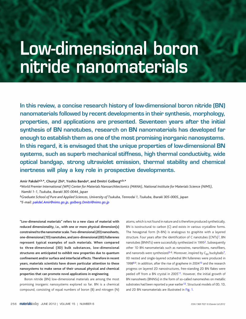
Low-dimensional boron nitride nanomaterials
“Low-dimensional materials” refers to a new class of material with
reduced dimensionality, i.e., with one or more physical dimension(s)
constrained to the nanometer scale. Two-dimensional (2D) nanosheets,
one-dimensional (1D) nanotubes, and zero-dimensional (0D) fullerenes
represent typical examples of such materials. When compared
to three-dimensional (3D) bulk substances, low-dimensional
structures are anticipated to exhibit new properties due to quantum
confinement and/or surface and interfacial effects. Therefore in recent
years, materials scientists have drawn particular attention to these
nanosystems to make sense of their unusual physical and chemical
properties that can promote novel applications in engineering.
Boron nitride (BN) low-dimensional materials are among the most
promising inorganic nanosystems explored so far. BN is a chemical
compound, consisting of equal numbers of boron (B) and nitrogen (N)
atoms, which is not found in nature and is therefore produced synthetically.
BN is isostructural to carbon (C) and exists in various crystalline forms.
The hexagonal form (h-BN) is analogous to graphite with a layered
structure. Four years after the identification of C nanotubes (CNTs)1, BN
nanotubes (BNNTs) were successfully synthesized in 19952. Subsequently
other 1D BN nanomaterials such as nanowires, nanoribbons, nanofibers,
and nanorods were synthesized3-6. Moreover, inspired by C60 buckyballs7,
0D nested and single-layered octahedral BN fullerenes were produced in
19988,9. In addition, after the rise of graphene in 200410 and the research
progress on layered 2D nanostructures, free-standing 2D BN flakes were
peeled off from a BN crystal in 200511. However, the initial growth of
BN nanosheets (BNNSs) in the form of so-called nanomeshes on metallic
substrates had been reported a year earlier12. Structural models of 0D, 1D,
and 2D BN nanomaterials are illustrated in Fig. 1.
In this review, a concise research history of low-dimensional boron nitride (BN) nanomaterials followed by recent developments in their synthesis, morphology, properties, and applications are presented. Seventeen years after the initial synthesis of BN nanotubes, research on BN nanomaterials has developed far enough to establish them as one of the most promising inorganic nanosystems. In this regard, it is envisaged that the unique properties of low-dimensional BN systems, such as superb mechanical stiffness, high thermal conductivity, wide optical bandgap, strong ultraviolet emission, thermal stability and chemical inertness will play a key role in prospective developments.
Amir Pakdela,b,*, Chunyi Zhia, Yoshio Bandoa, and Dmitri Golberga,b,*aWorld Premier International (WPI) Center for Materials Nanoarchitectonics (MANA), National Institute for Materials Science (NIMS), aNamiki 1-1, Tsukuba, Ibaraki 305-0044, JapanbGraduate School of Pure and Applied Sciences, University of Tsukuba, Tennodai 1, Tsukuba, Ibaraki 305-0005, Japan
*E-mail: [email protected], [email protected]
MT156p256_265.indd 256 12/06/2012 10:33:26

Low-dimensional boron nitride nanomaterials REVIEW
JUNE 2012 | VOLUME 15 | NUMBER 6 257
Synthesis of BNNTs Most of the techniques known for the growth of CNTs have been
modified to synthesize BNNTs as well. These methods can be classified
into two broad categories: (1) high temperature synthesis (> 2000 °C),
such as arc discharge and laser ablation; (2) medium/low temperature
synthesis (< 2000 °C), such as carbothermal methods, ball milling, and
chemical vapor deposition (CVD).
Arc discharge The first successful synthesis of BNNTs was reported in 1995 by Chopra
et al.2. They used a tungsten electrode filled with h-BN powder as anode
and a copper (Cu) electrode as cathode to produce multi-walled BNNTs
which included metallic particles at their tips. Subsequently, single- and
double-walled BNNTs were synthesized by arcing Hafnium diboride
(HfB2) electrodes in an inert atmosphere13. Double-walled BNNTs were
mass-produced by arcing B electrodes containing nickel (Ni) or cobalt
(Co) in an N2 atmosphere14. Later in 2006, a continuous process using an
arc-jet technique at high temperature (5000 – 20 000 K) was developed
as a promising method for the large-scale production of single- and
multi-walled BNNTs15. A mixture of h-BN and catalyst metal powders
was used as precursor and a combination of argon (Ar) and N2 formed
the plasma gas. A similar technique had been employed earlier in our
group, but the obtained product was a mixture of BN, C and composite
nanotubes of BN−C16.
Laser ablationA laser assisted technique was used by Golberg et al.17 in 1996 to
generate multi-walled BNNTs. Single-crystal samples of cubic or
hexagonal BN (c-BN, h-BN) were laser heated for a short time in a
diamond anvil cell under high pressures of N2. However a large quantity
of BN flakes and particles were also included in the product. Further
development of this method resulted in the synthesis of single-, double-,
and triple-walled BNNTs by using a mixture of BN, Ni, and Co powders
in an inert atmosphere18. Later, a rotating catalyst-free BN target in a
continuous laser ablation reactor under N2 was used to produce bulk
quantities of BNNTs19. Subsequently, high yields of single- and multi-
Fig. 1 Structural models of low-dimensional BN nanostructures: (a) single-layered nanosheet (2D), (b) single-walled nanotube (1D), (c) single-shelled fullerene (0D).
(b)(a) (c)
Fig. 2 (a) HRTEM images of nanotubes with 1 – 6 walls. (b) Schematic of the substitutional reactions in CNTs, developed with temperature (T) and time (t). (i) Void formation in C layers due to oxidation of C with O2 or metal oxides (MOs). (ii) More voids formation and outer layers peeling off. (iii) Reaction of B2O3 and N2 with C to form BN domains. (iv) End of the substitution reactions. (v) Shrinkage of the BN layers by the rearrangement of B and N atoms to eliminate large voids. Reprinted with permission from25. © 2006 American Institute of Physics.
(a)
(b)
MT156p256_265.indd 257 12/06/2012 10:33:28

REVIEW Low-dimensional boron nitride nanomaterials
JUNE 2012 | VOLUME 15 | NUMBER 6258
walled BNNTs were obtained based on the vaporization of h-BN targets
via a continuous CO2 laser under N2 flow at ~3500 K20. However, the
product contained unwanted morphologies besides tubular structures.
Carbothermal methodsAn alternative method to synthesize BNNTs was developed by Han et al.21
in 1998. It was based on the idea of turning CNTs to BNNTs through
the substitution of C atoms with B and N atoms. Boron trioxide (B2O3)
powders covered by CNTs were under N2 flow at 1500 ºC inside an
induction furnace. While the CNTs were oxidized by B2O3, B and N
atoms filled the generated vacancies in the hexagonal structure. As a
result, multi-walled BNNTs were produced with diameters similar to
those of the initial CNTs22. This technique was further optimized to
produce single-walled BNNT bundles by using pure single-walled CNTs
as the precursor23. However, the product included B−C and B−C−N
compound single-walled nanotubes as well. Further work demonstrated
that C content in the product can be reduced by adding an extra oxidizing
agent to the system24. This technique could also lead to the generation
of BNNTs with smaller diameters than those of the starting CNTs25.
Transmission electron microscope (TEM) images of BNNTs with 1 to 6
shells and a schematic of the substitution process are illustrated in Fig. 2.
In another approach, Bartnitskaya et al.26 employed boron carbide
(B4C) as the C source instead of CNTs. The carbothermal reduction
of BxOy and the simultaneous nitriding at 1100 – 1450 °C resulted in
the production of BN tubes with large diameters and a bamboo-like
structure. Also, synthesis of multi-walled BNNTs by using boric acid
(H3BO3) and active carbon or CNTs in the presence of iron compounds
under ammonia (NH3) atmosphere has been reported27.
Mechanothermal methodsThe initial mechanothermal method for the production of BNNTs
was pioneered by Chen et al.28 in 1999. It included ball milling of B
powder in NH3 gas, followed by thermal annealing at 1000 – 1200 ºC
under N2 or Ar. The BN products had a bamboo-like structure with
50 – 75 nm external diameters. They also applied this process to h-BN
powder, obtained bamboo-like nanotubes with diameters ranging from
~11 to ~280 nm, and suggested that ball milling of h-BN powder
could generate highly disordered or amorphous nanostructures, which
could promote nucleation and growth of BNNTs after annealing at
high temperatures29. It has been also proposed that surface diffusion in
milled powder could be the key factor for growing BNNTs through a tip-
growth model, due to the presence of Fe particles at the tip of the BN
tubes (Fig. 3)30. Further development of this method by other research
groups resulted in synthesis of BNNTs with diameters of 5 – 30 nm31
and 40 – 60 nm32, and lengths of several μm, depending on the chemical
composition of initial powders and synthesis temperature. High yields of
multi-walled BNNTs with diameters < 10 nm were synthesized by Yu et
al.33 using a ball milling-annealing process in which amorphous B was
ball-milled for 150 h and annealed at 1200 °C under NH3. The produced
nanotubes had no trace of metallic particles, which may suggest a root-
growth mechanism for their growth.
Chemical vapor deposition (CVD)The pioneering work on the CVD synthesis of BNNTs, by using borazine
(B3H6N3) as precursor and Ni2B particles as catalyst at 1000 – 1110 °C,
was carried out by Lourie et al.34 in 2000. The nanotubes often possessed
bulbous, flag-like, and/or club-like tips. An efficient CVD route to
synthesize significant amounts of BNNTs was developed in our group
through heating a mixture of B, MgO, and FeO powders to 1300 °C.
The growth vapors were transported by an Ar flow to the reaction
chamber, where a substrate was placed and heated to 1550 °C under
NH3 flow. BNNTs (both cylindrical and bamboo-like) with diameters of
20 – 100 nm were produced by this method35. Recently this technique
has successfully been applied to generate high yields of thin BNNTs with
an average diameter of 10 nm by using a mixture of Li2O and B powders
as precursor36. There are several reports on the development of various
CVD techniques and using different precursor materials to obtain BNNTs
at 450 – 1200 °C in different shapes and sizes37-40.
An interesting feature of the CVD process is the growth of thin
films and coatings made of nanostructured materials. Fe-particle-
functionalized substrates were used by Yap’s group41 for growing BNNT
bundles at 600 °C. They used a plasma-enhanced pulsed-laser deposition
technique with a negative substrate bias voltage to generate the reactive
condition for tubes growth perpendicular to the substrates (Fig. 4). A
plasma technique was also used to produce highly-ordered multi-walled
BNNT arrays42. Later, conventional horizontal tube furnaces were used to
synthesize BNNT films by thermal CVD43. Very recently a comprehensive
study by Pakdel et al.44 demonstrated the effect of process variables on
the CVD growth of films of BNNTs with different sizes and morphologies
(Fig. 5). In spite of the success of CVD techniques in the production of
milligram-scale quantities of BNNTs to date, these methods still need
further development to be comparable with CVD-grown hundreds of
grams of CNTs in a single experimental run45.
Synthesis of BNNSs The formation of a highly regular mesh of h-BN on a rhodium
(Rh) single crystalline surface by self-assembly was performed by
Fig. 3 TEM image of a bamboo-like BNNT, containing a metallic tip, synthesized by ball milling. Reprinted with permission from30. © 1999 Elsevier.
MT156p256_265.indd 258 12/06/2012 10:33:31

Low-dimensional boron nitride nanomaterials REVIEW
JUNE 2012 | VOLUME 15 | NUMBER 6 259
Fig. 4 SEM images of BNNT bundles grown at a substrate bias of (a) −380 V and (b) −450 V and (c) their corresponding bundling configurations (left and right, respectively). (d) Patterned growth of BNNTs. Reprinted with permission from41. © 2005 American Chemical Society.
(b)(a)
(c) (d)
Fig. 5 Effect of growth temperature and catalyst content on the morphology of BNNT films, as revealed by SEM. From reference44.
(a)
(b)
(c) (e)
(d)
MT156p256_265.indd 259 12/06/2012 10:33:32

REVIEW Low-dimensional boron nitride nanomaterials
JUNE 2012 | VOLUME 15 | NUMBER 6260
Corso et al.46 in 2004. The preparation procedure consisted of
exposing the atomically clean Rh(111) surface at 800 °C to B3H6N3
vapor inside an ultrahigh vacuum chamber and consecutive cooling
to room temperature. The regular mesh structure was observed by
scanning tunneling microscopy (STM), as shown in Fig. 6. It was
suggested that the hole formation is driven by the lattice mismatch
of the film and the Rh substrate.
Synthesis and characterization of 2D nanosheets in general, and
BNNSs in particular, are rather new topics in materials science and the
related reports are still very limited, as categorized in this section.
Micromechanical cleavage The pioneering procedure to obtain atomic sheets of h-BN was the
micromechanical cleavage technique, reported by Novoselov et al.11 in 2004.
In this method, layers of h-BN are peeled off with adhesive tapes and attached
to a substrate. Atomic force microscopy (AFM) and TEM investigations of
BNNSs prepared by this method in Zettl’s group revealed the clean well-
ordered nanosheets, with thicknesses between 3.5 and 80 nm47.
Chemical exfoliation (sonication)Preparation of mono- and few-layered nanosheets from a single-crystalline
h-BN by a chemical-solution-derived method was first accomplished
by Han et al.48 in 2008. The h-BN crystal was sonicated in an organic
solution to break up into few-layered h-BN sheets. Fig. 7 displays typical
TEM images of the obtained BNNSs. Later, the exfoliation of nanosheets
from BN particles dispersed in a strong polar solvent was performed in
our group via vigorous sonication-centrifugation49. The solvent facilitated
the exfoliation, due to strong interactions between its polar molecules
and the BN surface. Milligram levels of pure BNNSs with 2 − 10 nm
thicknesses were achieved. Different solvents have been employed in
chemical exfoliation methods to promote BNNSs formation50,51.
High-energy electron irradiation Fabrication of freestanding single-layered BNNSs by controlled electron
irradiation through a layer-by-layer sputtering process in situ inside a
TEM was reported by Jin et al.52 and Meyer et al.53 in 2009. First, h-BN
nano-flakes and powders underwent mechanical cleavage to obtain
h-BN sheets with a reduced number of layers. Then, the h-BN nano-
flakes were further thinned down to monolayers by focusing an intensive
Fig. 6 A constant-current STM image of the BN nanomesh formed on a Rh(111) surface. Two steps on the Rh(111) surface cross the image. The black features are defects in the mesh, one of which is shown with different contrast in the inset. Reprinted with permission from46. © 2004 The American Association for the Advancement of Science.
Fig. 7 (a) Low-magnification and (b) HRTEM image of a BN sheet with two atomic layers; (c) HRTEM image of a multi-layered BN sheet. Inset III is a simulated image based on a structural model in which a 13.8° rotated BN sheet is overlapped with another BN sheet. Reprinted with permission from48. © 2008 American Institute of Physics.
(b)(a) (c)
MT156p256_265.indd 260 12/06/2012 10:33:35

Low-dimensional boron nitride nanomaterials REVIEW
JUNE 2012 | VOLUME 15 | NUMBER 6 261
electron beam onto the specimen. By scanning the electron beam under
a manual control, h-BN nano-flakes were burnt layer-by-layer until h-BN
monolayers were obtained.
Wet chemical reactions BNNSs were prepared through chemical reactions of boric acid (H3BO3)
and urea (CO(NH2)2) at 900 °C under N2 in Rao’s group in 201054. Few-
layered BN sheets formed due to the following reactions:
2H3BO3 → B2O3 + 3H2O
CO(NH2)2 → NH3 + HNCO
B2O3 + 2NH3 → 2BN + 3H2O
The authors claimed to have controlled the number of layers through
variations in the concentration of the reacting materials. Namely, the
thickness of the sheets decreased with increasing the urea concentration
in the reaction mixture.
Ball millingHigh yields of BNNSs were obtained from ball milling of h-BN
powders under an N2 atmosphere by Li et al.55 in 2011. They tailored the
ball milling conditions to generate gentle shear forces that resulted in
production of high-quality BNNSs. The milled samples were diluted with
benzyl benzoate and sonicated for 0.5 h to produce thin sheets of BN
(Fig. 8). These authors mentioned that their method could be applicable
to produce nanosheets from any layered materials.
Chemical vapor depositionAn alternative technique to prepare BNNSs is CVD. Relatively large
quantities of thick h-BN sheets were synthesized via a catalyst-free CVD
process at 1100 – 1300 °C by Gao et al.56 in 2009. B2O3 and melamine
powders were mechanically mixed and placed in an induction furnace. The
temperature was raised to 1000 – 1300 °C under N2 flow and after ~1 h
BN sheets with thicknesses of 25 – 50 nm (depending on the synthesis
temperature) were obtained. Later, a multi-step thermal catalytic CVD
method was employed to fabricate h-BN films, consisting of 2 – 5 atomic
layers, under ammonia borane (NH3−BH3) flow on a Cu foil as the
substrate57. Few-layered h-BN films were also synthesized by ambient
pressure CVD on polycrystalline Ni films with thicknesses of ~5 – 50 nm,
depending on the growth conditions58. The h-BN grew continuously on the
entire Ni surface and the regions with uniform thicknesses were up to 20
μm in lateral size. In another set of experiments, reaction of polyborane
decaborane (B10H14) with NH3 formed BNNSs on either polycrystalline Ni
or Cu foils at 1000 °C59. Very recently, monolayer h-BN was grown on Cu
foils by using NH3−BH3 via low pressure CVD with two heating zones60.
Vertically-aligned BNNSs on silicon (Si) substrates were prepared
by Yu et al.61 via microwave plasma CVD from a gas mixture of
BF3−N2−H2. The thickness of the nanosheets could be controlled
between ~5 and 20 nm by changing the growth conditions. In another
approach, Pakdel et al.62,63 developed a thermal CVD technique to
manufacture vertically-aligned pure and C-doped BNNSs on Si/SiO2
substrates by using B, MgO, and FeO powders under NH3 flow in a
horizontal tube furnace (Fig. 9). The majority of the nanosheets was less
than 5 nm in thickness, and by increasing the growth time and/or the
growth temperature, larger-sized nanosheets were formed.
Fig. 8 SEM images and corresponding diagrams illustrating two observed exfoliating mechanisms under the shear force created by milling balls: (a), (b) cleavage from the edge of an h-BN particle; (c), (d) thin sheets peeling off the top surface of an h-BN particle. Reprinted with permission from55. © 2011 Royal Society of Chemistry.
(b)
(a) (c)
(d)
Table 1. The crystallographic information of h-BN and graphite
Material Crystal structure
Nearest neighbor distance
Lattice parameters
Inter-layer spacing
h-BN hexagonal 0.144 nm a: 0.250 nmc: 0.666 nm
0.333 nm
Graphite hexagonal 0.142 nm a: 0.246 nmc: 0.670 nm
0.335 nm
MT156p256_265.indd 261 12/06/2012 10:33:39

REVIEW Low-dimensional boron nitride nanomaterials
JUNE 2012 | VOLUME 15 | NUMBER 6262
StructureGenerally, BN nanomorphologies can be considered as h-BN layers
formed in different ways. BNNTs can be defined as cylinders of concentric
h-BN layers (from one to many layers), with diameters in the nanometer
scale. The structure of multi-walled BN tubes can be described by two
different models. In the “Russian Doll” model, h-BN sheets are arranged
in separate concentric cylinders (e.g., a single-walled nanotube within a
larger one, and so on), and in the “Parchment” model, a single sheet of
h-BN is rolled around itself, resembling a scroll of parchment or a rolled
newspaper64. However, multi-walled nanotubes are usually believed to
be made of concentric tubes, rather than a spiraling layer, due to energy
considerations. As for BNNSs, they may be depicted as graphene layers,
in which C atoms have been fully substituted by alternating B and N
atoms. Within each h-BN layer, atoms are bound together by strong
covalent bonds, while there are weak van der Waals forces between
different layers. The crystallographic parameters of h-BN and graphite
are almost identical, as summarized in Table 165.
Unlike the popular monolayer graphenes and single-walled CNTs,
their corresponding BN sister systems have rarely been observed66,67,
due to the peculiar B−N stacking characteristics. The hexagons of
neighboring planes in h-BN are superposed, i.e., B and N atoms are in
succession along the c-axis, while in graphite, they are shifted by half a
hexagon. Moreover, due to the difference in electronegativity of B and
N, the B−N bonds in BN materials are partially ionic, in contrast with
the purely covalent C−C bonds in graphitic structures. These can lead
to the so-called “lip−lip” interactions between neighboring layers/shells
in BN nanostructures, i.e., chemical bonds form as bridges or “spot-
welds” between the atoms of adjacent layers/shells. This phenomenon
contributes to a metastable energy minimum through decreasing the
number of dangling bonds at the edges/tips and reducing the “frustration”
effect (i.e., when B−B and N−N bonds form instead of the energetically
more favorable B−N bonds). Therefore, formation of multi- layers/shells
stabilizes the whole structure68,69.
Ab initio calculations have demonstrated that the folding of an isolated
h-BN sheet onto a tubular BN is slightly more favorable than that of
graphene onto a CNT of the same radius, owing to a “buckling” effect
which stabilizes the BN tubular structure. First-principles calculations
indicate that in the minimum energy structure, all B atoms are arranged
in one cylinder and all N atoms in a larger concentric one, and due
to charge transfer from B to N, the buckled tubular structure forms a
dipolar shell. As a result, each B atom is virtually located on a plane
formed by its three neighboring N atoms, so that the sp2 environment
Fig. 9 SEM images of the BNNS coatings synthesized at 900 – 1200 °C for 30 and 60 minutes. The scale bar is 200 nm. From reference62.
(b)(a) (c) (d)
(f)(e) (g) (h)
MT156p256_265.indd 262 12/06/2012 10:33:40

Low-dimensional boron nitride nanomaterials REVIEW
JUNE 2012 | VOLUME 15 | NUMBER 6 263
for the B atom in the planar hexagonal structure is restored. This buckling
effect significantly reduces the occupied band energy in the case of BN
compounds; thus, folding an h-BN sheet into a tube is energetically more
favorable than in the case of graphene. Also, the calculated energy of
dangling bonds associated with opened BN strips is much larger than that
of tubes, that it is energetically more favorable to preserve the cylindrical
geometry despite the elastic energy resulting from the curvature70.
Polygonization of cross sections is favorable in multi-walled BNNTs
since the B−N−B−N stacking order across a BN tube could be better
preserved within multiple polygonized shells with flat facets71. Such
stacking can be broken in cylindrical multi-walled nanotubes due to
the existence of different circumferences in consecutive shells. In fact,
a multi-walled nanotube with a polygonal cross section can have a
lower energy than a nanotube with a circular cross section. This energy
reduction occurs because the flat sections of the nanotube can have a
coherent interface with no tensile strain. But, when the cross section
is circular it is not possible to maintain a coherent interface without
an excessive amount of tensile strain, due to the difference in the
circumference of consecutive shells72.
Properties and applicationsBulk h-BN has been a matter of interest for a long time due to its low
density, high thermal conductivity, electrical insulation, superb oxidation
resistance, excellent inertness (i.e., passivity to reactions with acids,
alkalis, and melts), and low friction coefficient. BNNTs and nanosheets,
as inheritors of h-BN, also possess these advantageous properties73.
Electronic and optical propertiesBN nanostructures are generally recognized as insulators with wide
bandgaps of 5.0 – 6.0 eV. The theoretical analysis of electronic properties of
BNNTs and nanosheets reviewed by Arenal et al.74 showed their bandgap
to be first-order independent of the details of the atomic structure.
This explains the so-called stability of the bandgap in BNNTs which
indeed hardly depends on curvature and helicity70, except in the limit
of very small diameters. Recent experimental studies by Lee et al.75and
Pakdel et al.63 have pointed out optical bandgaps of ~6 and ~5.7 eV for
BNNTs and BNNSs, respectively, which approach that of h-BN single
crystals. This insulating behavior of BN nanostructures encourages their
applications as protective shields encapsulating nanomaterials. In this
regard, considerable research has been performed to fill BNNTs during
or after the synthesis with fullerenes or with crystalline compounds, such
as cobalt, iron-nickel and magnesium oxide76-78. However, Terrones et
al.79 have theoretically and experimentally demonstrated that BN
nanoribbons with zigzag edges can show metallic behavior. Their porous
BN nanospheres showed stable field emission properties at low turn-
on voltages (e.g., 1 – 1.3 V/μm) due to the presence of these ribbons
protruding from the surface of the spheres. Such BN nanostructures may
find applications as catalysts or field-emitters in the future. Moreover BN
nanostructures exhibit distinctive violet or ultraviolet (UV) luminescence
emissions, which promote their application in downsized UV lasing
devices for sterilization, surgery, photocatalysis, and optical storage45.
Thermal propertiesh-BN possesses remarkable thermal conductivity and high specific heat.
Theoretical calculations by Xiao et al.80 demonstrated high specific heat
of BNNTs and predicted that their thermal conductivity is higher than
that of CNTs. They also showed that thermal conductance of single-
walled BNNTs at low temperatures is independent of the tube diameter
and chirality81. A recent study indicates that the strong phonon-phonon
scattering in h-BN is the cause for its lower thermal conductivity
compared to graphite, however, reduction in such scattering in a
single layer BN sheet leads to a substantial increase in its conductivity
(>600 W/m/K at room temperature)82. Experimentally, Chang et al.83
measured the thermal conductivity values for BNNTs to be ~350 W/m/K
Fig. 10 (a) Water contact angles of BNNS coatings synthesized at 900 − 1200 °C, indicating the change in their wettability from partial wetting to nonwetting. (b) Photograph of spherical water droplets on a BNNS film. From reference62.
(b)(a)
MT156p256_265.indd 263 12/06/2012 10:33:43

REVIEW Low-dimensional boron nitride nanomaterials
JUNE 2012 | VOLUME 15 | NUMBER 6264
at room temperature and demonstrated that if they were mass-loaded
externally and heterogeneously with heavy molecules (e.g., C9H16Pt)
they would possess asymmetric axial thermal conductance properties.
Thus, BNNT thermal rectifiers were suggested to have substantial
implications for diverse nanoscale calorimeters, microelectronic
processors, macroscopic refrigerators, and energy-saving buildings.
Thermal stability experiments on multi-walled BNNTs were performed
by Golberg et al.84 and indicated excellent oxidation resistance up to
830 °C in air. Moreover, thermogravimetric analysis showed that the
onset temperature for the oxidation of BNNTs (800 °C) was much higher
than that of CNTs (400 °C) under the same conditions. Later it was
shown that thin BNNTs with diameters smaller than 20 nm can resist
oxidation up to 900 °C85.
Mechanical propertiesTheoretical studies by Hernandez et al.86 revealed the elastic modulus of
BNNTs to vary between ~0.84 and ~0.91 TPa with diameters ranging from
0.81 to 2.08 nm. Chopra and Zettl87 estimated the elastic modulus of a
cantilevered individual double-walled BNNT by measuring the amplitude
of the thermal-induced vibrations in a TEM at room temperature. They
found a value of 1.22 ± 0.24 TPa, which is similar to the elastic modulus
of CNTs. Subsequently, an electric-field-induced resonance method in
TEM was utilized to calculate elastic modulus values between 0.51 and
1.03 TPa88. More recently, Golberg’s group performed extensive in situ
TEM bending and tensile experiments on individual multi-walled tubes
with diameters of 40 – 100 nm and estimated their elastic modulus as
0.5 – 0.6 TPa71 or up to 1.3 TPa89, and their tensile strength as 33 GPa.
However, in the case of bamboo-like BNNTs, the elastic modulus and
tensile strength were estimated as 225 GPa and 8 GPa, respectively90.
Superior mechanical properties and thermal conductivity of BN
nanostructures make them attractive as nanofillers in composite materials. For
instance, BNNTs can reinforce polymer matrices and improve their thermal
conductivity, while transparency of the polymers is preserved. Zhi et al.91
initiated research on polymer matrix composites reinforced by BNNTs and
showed an effective improvement in elastic modulus of polystyrene and
polymethyl methacrylate (PMMA) by ∼20 % with addition of only 1 wt.%
of nanotubes. A very recent work on nanomechanical characterization of
single-walled BNNTs revealed their axially strong, but radially supple,
characteristics and suggested that they might be superior to single-walled
CNTs as reinforcing additives for nanocomposite applications92.
Wetting propertiesWhile h-BN films are partially wetted by water with contact angle
of ~50°, BNNT films can achieve superhydrophobic state with water
contact angle exceeding 150°93,94. In a systematic approach, the present
authors succeeded in growing partially vertically aligned BNNSs on Si
substrates with controllable water-repellency levels62. As a result, water
contact angles from ~51° to ~159° were obtained, indicating a significant
change from hydrophilicity to superhydrophobicity. Due to outstanding
chemical intentness of BN, the pH value of water did not affect the
wetting characteristics of BNNS and BNNT films62,93. Therefore, BN
nanostructure films are anticipated to find industrial applications in
water-repelling, anti-fouling, self-cleaning, and anti-corrosion systems.
Conclusion and prospectsAn overview of research on low dimensional BN nanomaterials in
terms of synthesis, properties, and prospective applications has been
presented. Despite the interesting properties and promising outlook of
BN nanostructures, the research progress on the fundamental physical
aspects and potential applications of these nanomaterials has been
rather limited so far, especially when one compares them with the well-
explored C nanosystems (i.e., CNTs, graphene, and fullerene family). This
might be attributed to the difficulties involved in the mass-production
of low dimensional BN nanomaterials with high purity and good
crystallinity, which hinders their immediate applications in industry.
However, the possibility of morphological manipulation in some
synthetic routes (e.g., CVD) can motivate further work toward new
functions and applications, such as chemically inert surfaces with
controllable levels of water repellency. Moreover, aside from the
unique properties of BN nanostructures such as homogeneous electrical
insulation, wide optical bandgap and deep UV emission, excellent
thermal stability and oxidation resistance, good thermal conductivity
and outstanding stiffness, new properties are likely to be discovered in
tailored BN nanostructures.
h-BN has been considered as one of the best substrates for maintaining
the excellent transport behavior of graphene, because it provides
extraordinarily flat graphene layers that significantly reduce electron−
hole puddles as compared to SiO295. By reducing the charge fluctuations,
the low density regime and the Dirac point can be more readily accessed.
Graphene devices on h-BN substrates have demonstrated mobilities and
carrier inhomogeneities that are almost an order of magnitude better than
devices on SiO296. A hybrid structure consisting of h-BN and graphene
would enable the physical properties of graphene-based structures to be
tailored97,98. Such a system could be useful for various applications, such
as field-effect transistors for radio-frequency apparatus99.
Further applications of BN nanomaterials could be in nanomedicine
due to their good biocompatibility, scanning probe microscopy as ultrathin
stiff tips, new generations of semiconducting materials with adjustable
bandgap through doping of other elements into BN structures, and
manufacturing hybrid nanostructures through surface functionalization
of BN nanomaterials with nanoparticles of other materials. Recently,
functionalized BNNTs have been tested in vitro on fibroblast cells, and
demonstrated optimal cytocompatibility even at high concentrations in
the culture medium100.
Acknowledgments The authors acknowledge the financial support of the World Premier
International (WPI) Center for Materials Nanoarchitectonics (MANA) of
MT156p256_265.indd 264 12/06/2012 10:33:43

Low-dimensional boron nitride nanomaterials REVIEW
JUNE 2012 | VOLUME 15 | NUMBER 6 265
REFERENCES
1. Iijima, S., Nature (1991) 354, 56.
2. Chopra, N. G., et al., Science (1995) 269, 966.
3. Yong, J. C., et al., Nanotechnology (2006) 17, 786.
4. Chen, Z. G., et al., ACS Nano (2008) 2, 2183.
5. Qiu, Y. J., et al., Nanotechnology (2009) 20, 345603.
6. Zhang, H. Z., et al., J Am Ceram Soc (2006) 89, 675.
7. Kroto, H. W., et al., Nature (1985) 318, 162.
8. Stephan, O., et al., Appl Phys A-Mater (1998) 67, 107.
9. Golberg, D., et al., Appl Phys Lett (1998) 73, 2441.
10. Novoselov, K. S., et al., Science (2004) 306, 666.
11. Novoselov, K. S., et al., P Natl Acad Sci USA (2005) 102, 10451.
12. Corso, M., et al., Science (2004) 303, 217.
13. Loiseau, A., et al., Phys Rev Lett (1996) 76, 4737.
14. Cumings, J., and Zettl, A., Chem Phys Lett (2000) 316, 211.
15. Lee, C. M., et al., Curr Appl Phys (2006) 6, 166.
16. Shimizu, Y., et al., Thin Solid Films (1998) 316, 178.
17. Golberg, D., et al., Appl Phys Lett (1996) 69, 2045.
18. Yu, D. P., et al., Appl Phys Lett (1998) 72, 1966.
19. Lee, R. S., et al., Phys Rev B (2001) 64, 121405.
20. Arenal, R., et al., J Am Chem Soc (2007) 129, 16183.
21. Han, W. Q., et al., Appl Phys Lett (1998) 73, 3085.
22. Golberg, D., et al., Solid State Commun (2000) 116, 1.
23. Golberg, D., et al., Chem Phys Lett (1999) 308, 337.
24. Golberg, D., et al., Chem Phys Lett (2000) 323, 185.
25. Han, W. Q., et al., Appl Phys Lett (2006) 89, 173103.
26. Bartnitskaya, T. S., et al., Jetp Lett+ (1999) 69, 163.
27. Deepak, F. L., et al., Chem Phys Lett (2002) 353, 345.
28. Chen, Y., et al., Chem Phys Lett (1999) 299, 260.
29. Chen, Y., et al., Appl Phys Lett (1999) 74, 2960.
30. Chadderton, L. T., and Chen, Y., Phys Lett A (1999) 263, 401.
31. Tang, C. C., et al., Chem Phys Lett (2002) 362, 185.
32. Bae, S. Y., et al., Chem Phys Lett (2003) 374, 534.
33. Yu, J., et al., Chem Mater (2005) 17, 5172.
34. Lourie, O. R., et al., Chem Mater (2000) 12, 1808.
35. Tang, C., et al., Chem Commun (2002) 12, 1290.
36. Huang, Y., et al., D., Nanotechnology (2011) 22, 145602.
37. Kim, M. J., et al., Nano Lett (2008) 8, 3298.
38. Xu, L. Q., et al., Chem Mater (2003) 15, 2675.
39. Chen, X., et al., Appl Phys A-Mater (2005) 81, 1035.
40. Dai, J., et al., Chem Phys Lett (2007) 440, 253.
41. Wang, J. S., et al., Nano Lett (2005) 5, 2528.
42. Wang, X. Z., et al., Electrochim Acta (2007) 52, 2841.
43. Lee, C. H., et al., Nanotechnology (2008) 19, 455605.
44. Pakdel, A., et al., Nanotechnology (2012) 23, 215601.
45. Golberg, D., et al., Adv Mater (2007) 19 , 2413.
46. Corso, M., et al., Science (2004) 303, 217.
47. Pacile, D., et al., Appl Phys Lett (2008) 92, 133107.
48. Han, W. Q., et al., Appl Phys Lett (2008) 93, 223103.
49. Zhi, C. Y., et al., Adv Mater (2009) 21, 2889.
50. Warner, J. H., et al., ACS Nano (2010) 4, 1299.
51. Wang, Y., et al., J Mater Chem (2011) 21, 11371.
52. Jin, C. H., et al., S., Phys Rev Lett (2009) 102, 195505.
53. Meyer, J. C., et al., Nano Lett (2009) 9, 2683.
54. Nag, A., et al., ACS Nano (2010) 4, 1539.
55. Li, L. H., et al., J Mater Chem (2011) 21, 11862.
56. Gao, R., et al., J Phys Chem C (2009) 113, 15160.
57. Song, L., et al., Nano Lett (2010) 10, 3209.
58. Shi, Y. M., et al., Nano Lett (2010) 10, 4134.
59. Chatterjee, S., et al., Chem Mater (2011) 23, 4414.
60. Kim, K. K., et al., Nano Lett (2012) 12, 161.
61. Yu, J., et al., ACS Nano (2010) 4, 414.
62. Pakdel, A., et al., ACS Nano (2011) 5, 6507.
63. Pakdel, A., et al., J Mater Chem (2012) 22, 4818.
64. McNeish, T., et al., Phys Rev B (2008) 77, 235440.
65. Pauling, L., P Natl Acad Sci USA (1966) 56, 1646.
66. Lin, Y., et al., J Phys Chem C (2011) 115, 2679.
67. Arenal, R., et al., Nano Lett (2006) 6, 1812.
68. Blase, X., et al., Phys Rev Lett (1998) 80, 1666.
69. Charlier, J. C., et al., Appl Phys A-Mater (1999) 68, 267.
70. Blase, X., et al., Europhys Lett (1994) 28, 335.
71. Golberg, D., et al., Nano Lett (2007) 7, 2146.
72. Tibbetts, K., et al., Phys Rev B (2009) 80, 51037.
73. Golberg, D., et al., ACS Nano (2010) 4, 2979.
74. Arenal, R., et al., Adv Phys (2010) 59, 101.
75. Lee, C. H., et al., Chem Mater (2010) 22, 1782.
76. Mickelson, W., et al., Science (2003) 300, 467.
77. Bando, Y., et al., Chem Phys Lett (2001) 347, 349.
78. Golberg, D., et al., J Phys Chem B (2003), 107, 8726.
79. Terrones, M., et al, Nano Lett (2008) 8, 1026.
80. Xiao, Y., et al., Appl Phys Lett (2004) 84, 4626.
81. Xiao, Y., et al., Phys Rev B (2004) 69, 205415.
82. Lindsay, L., and Broido, D. A., Phys Rev B (2011) 84, 155421.
83. Chang, C. W., et al., Phys Rev Lett (2006) 97, 85901.
84. Golberg, D., et al., Scripta Mater (2001) 44, 1561.
85. Chen, Y., et al., Appl Phys Lett (2004) 84, 2430.
86. Hernandez, E., et al., Phys Rev Lett (1998) 80, 4502.
87. Chopra, N. G., and Zettl, A., Solid State Commun (1998) 105, 297.
88. Suryavanshi, A. P., et al., Appl Phys Lett (2004) 84, 2527.
89. Wei, X. L., et al., Adv Mater (2010) 22, 4895.
90. Tang, D. M., et al., ACS Nano (2011) 5, 7362.
91. Zhi, C., et al., Mat Sci Eng R (2010) 70, 92.
92. Zheng, M., et al., Small (2012) 8, 116.
93. Lee, C. H., et al., Langmuir (2009) 25, 4853.
94. Li, L. H., and Chen, Y., Langmuir (2010) 26, 5135.
95. Xue, J. M., et al., Nat Mater (2011) 10, 282.
96. Dean, C. R.;, et al., Nat Nanotechnol (2010) 5, 722.
97. Ci, L., et al., Nat Mater (2010) 9, 430.
98. Lin, T. Q., et al., J Mater Chem (2012) 22, 2859.
99. Wang, H., et al., IEEE Electr Device L (2011) 3, 1209.
100. Ciofani, G., et al., J Colloid Interf Sci (2012) 374, 308.
the National Institute for Materials Science (NIMS), Tsukuba, Japan. D.G.
acknowledges a funding Mega-Grant award for leading scientists tenable
at the National University of Science and Technology, Moscow, Russian
Federation, under the agreement No. 11.G34.31.0061.
MT156p256_265.indd 265 12/06/2012 10:33:44