Boron Nitride and graphene nanostructures: properties and ...
57
Boron Nitride and graphene nanostructures: properties and applications NanoCenter Seminar, Pittsburgh 17 th March 2009 NanoBio Spectroscopy Group, Dpto. Física de Materiales, Universidad del País Vasco, Centro Mixto CSIC-UPV/EHU and DIPC Edificio Korta, San Sebastián, Spain http://nano-bio.ehu.es E-mail: [email protected] Angel Rubio Boron Nitride and graphene nanostructures: properties and applications
Transcript of Boron Nitride and graphene nanostructures: properties and ...

Boron Nitride and graphene nanostructures: properties and applications NanoCenter Seminar, Pittsburgh 17th March 2009
NanoBio Spectroscopy Group, Dpto. Física de Materiales, Universidad del País Vasco,
Centro Mixto CSICUPV/EHU and DIPC Edificio Korta, San Sebastián, Spain
http://nanobio.ehu.es Email: [email protected]
Angel Rubio
Boron Nitride and graphene nanostructures: properties and applications

Boron Nitride and graphene nanostructures: properties and applications NanoCenter Seminar, Pittsburgh 17th March 2009
OUTLINE● Introduction to BN and other inorganic nanotubes● Structural, mechanical and Electronic properties:
doping , what is the bandgap of BN tubes? ● Optical absorption of the single BNsheet and
BNnanotubes (Abinitio calculations including manybody corrections (GW + BetheSalpeter)
● Luminiscence + Electric field effects (devices)● Graphene/Graphite● Conclusions
Boron Nitride and graphene nanostructures: properties and applications NanoCenter Seminar, Pittsburgh 17th March 2009
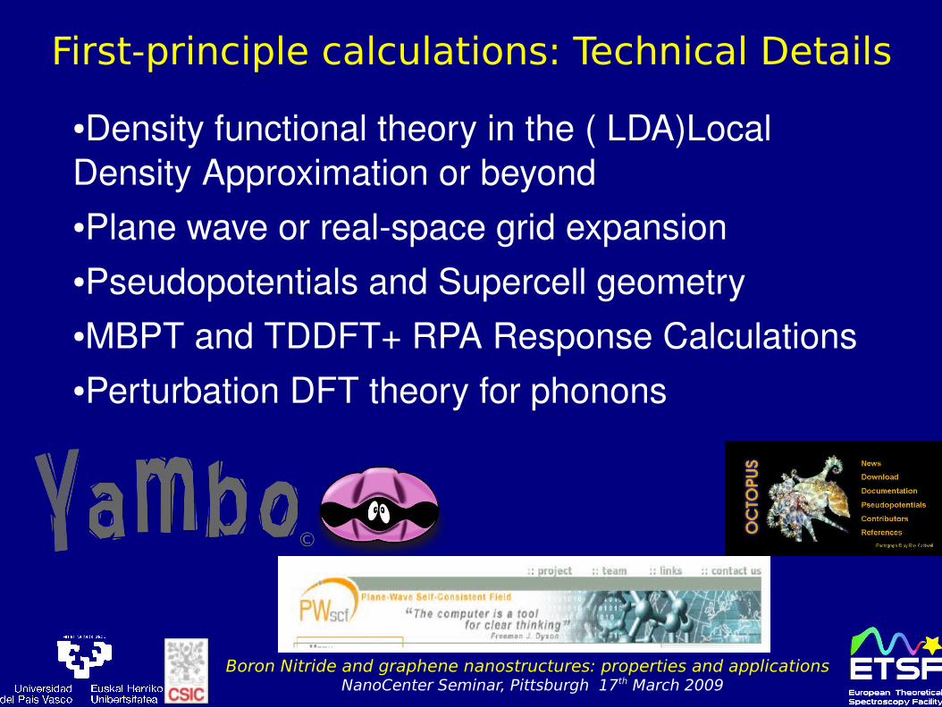
●Density functional theory in the ( LDA)Local Density Approximation or beyond●Plane wave or realspace grid expansion●Pseudopotentials and Supercell geometry●MBPT and TDDFT+ RPA Response Calculations●Perturbation DFT theory for phonons
First-principle calculations: Technical Details

Boron Nitride and graphene nanostructures: properties and applications NanoCenter Seminar, Pittsburgh 17th March 2009
Layered Materials
MoS2
WS2
NbS2
TaS2
VS2
ReS2
WSe2
MoSe2
Graphite
ChalcogenidesCarbon Nitride
Boron Nitride
OTHERS VO5, NiCl2 MgB2
Boron CarbonNitride......and your imagination!!!!
Superconductors, work together with Hardy Gross group, FU-Berlin

Boron Nitride and graphene nanostructures: properties and applications NanoCenter Seminar, Pittsburgh 17th March 2009
Layered Materials
Carbon Nanotubes
MoS2 Nanotubes
BN nanotubes
Fullerenes
BN cages
MoS2 cages

Boron Nitride and graphene nanostructures: properties and applications NanoCenter Seminar, Pittsburgh 17th March 2009
AR, Y. Miyamoto, S.G. Louie, and M.L. Cohen PRB (2004, 2005)
Composite NANOTUBES: stability
Boron Nitride and graphene nanostructures: properties and applications NanoCenter Seminar, Pittsburgh 17th March 2009
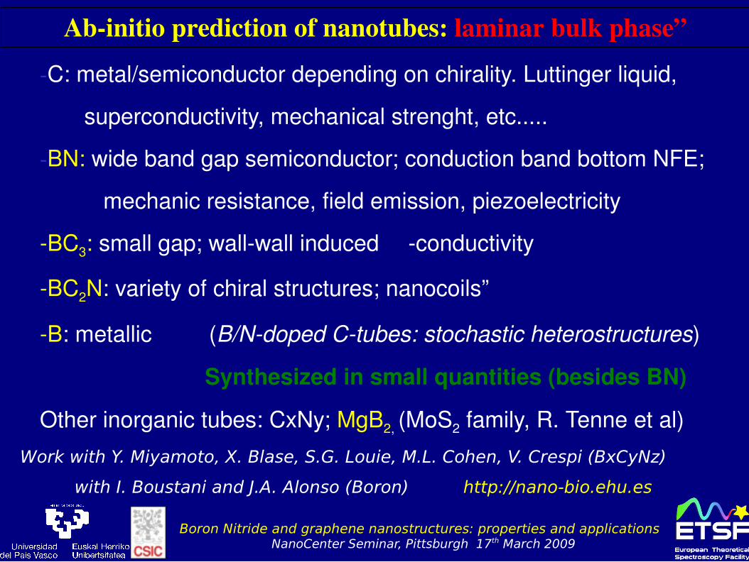
Abinitio prediction of nanotubes: laminar bulk phase”
C: metal/semiconductor depending on chirality. Luttinger liquid,
superconductivity, mechanical strenght, etc.....
BN: wide band gap semiconductor; conduction band bottom NFE;
mechanic resistance, field emission, piezoelectricity
BC3: small gap; wallwall induced � conductivity
BC2N: variety of chiral structures; nanocoils”
B: metallic (B/Ndoped Ctubes: stochastic heterostructures)
Synthesized in small quantities (besides BN)
Other inorganic tubes: CxNy; MgB2, (MoS2 family, R. Tenne et al)
Work with Y. Miyamoto, X. Blase, S.G. Louie, M.L. Cohen, V. Crespi (BxCyNz)
with I. Boustani and J.A. Alonso (Boron) http://nano-bio.ehu.es
Boron Nitride and graphene nanostructures: properties and applications NanoCenter Seminar, Pittsburgh 17th March 2009
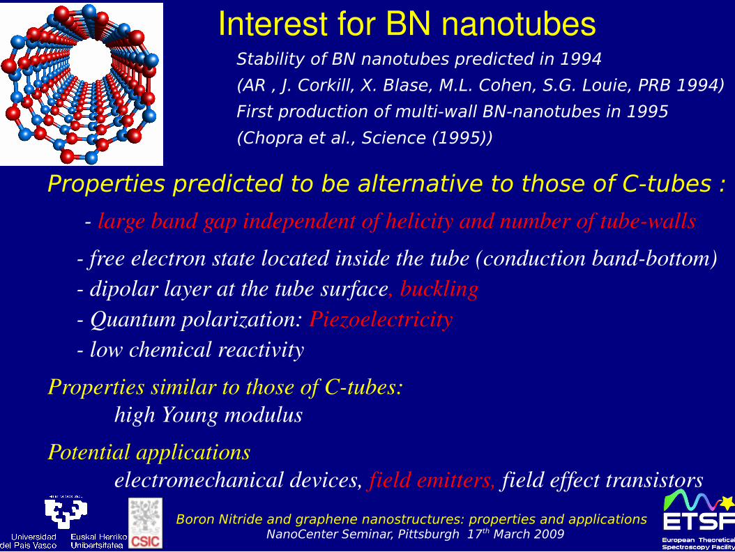
Interest for BN nanotubesStability of BN nanotubes predicted in 1994
(AR , J. Corkill, X. Blase, M.L. Cohen, S.G. Louie, PRB 1994)
First production of multi-wall BN-nanotubes in 1995
(Chopra et al., Science (1995))
Properties predicted to be alternative to those of C-tubes :
large band gap independent of helicity and number of tubewalls
free electron state located inside the tube (conduction bandbottom) dipolar layer at the tube surface, buckling Quantum polarization: Piezoelectricity low chemical reactivity
Properties similar to those of Ctubes:high Young modulus
Potential applications electromechanical devices, field emitters, field effect transistors

Boron Nitride and graphene nanostructures: properties and applications NanoCenter Seminar, Pittsburgh 17th March 2009
~1/r
Buckling of geometry optimized BNtubes:
dipolar shell structure
intertube interaction

Boron Nitride and graphene nanostructures: properties and applications NanoCenter Seminar, Pittsburgh 17th March 2009
0
L. Vaccarini, C. Goze, L. Henrard, E. Hernández, A. Loiseau, P. Bernier and A.R Carbon (2000);Phys Rev. Lett. (1998); Appl.Phys. A (1999)
Mechanical properties

Boron Nitride and graphene nanostructures: properties and applications NanoCenter Seminar, Pittsburgh 17th March 2009
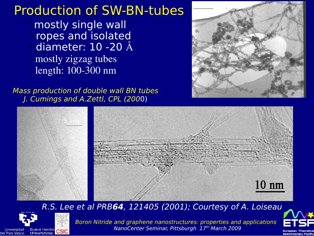
BN single wallnanotubes
R.S. Lee et al PRB64, 121405 (2001); Courtesy of A. Loiseau
Boron Nitride and graphene nanostructures: properties and applications NanoCenter Seminar, Pittsburgh 17th March 2009
200 nm
5 nm
Production of SW-BN-tubes• mostly single wall• ropes and isolated• diameter: 10 -20 Å• mostly zigzag tubes• length: 100300 nm
R.S. Lee et al PRB64, 121405 (2001); Courtesy of A. Loiseau
Mass production of double wall BN tubesJ. Cumings and A.Zettl, CPL (2000)
Boron Nitride and graphene nanostructures: properties and applications NanoCenter Seminar, Pittsburgh 17th March 2009
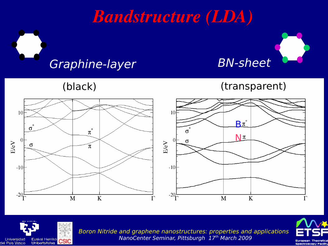
Bandstructure (LDA)
Graphine-layer BN-sheet
(transparent)(black)
N
B

Boron Nitride and graphene nanostructures: properties and applications NanoCenter Seminar, Pittsburgh 17th March 2009
Bandstructure (LDA)role of stacking....interlayer interaction
Graphite AB-stacking h-BN

Boron Nitride and graphene nanostructures: properties and applications NanoCenter Seminar, Pittsburgh 17th March 2009
Controversy about outofplane modes weakbonding????
Vibrational Properties: Raman and IR spectroscopy
Boron Nitride and graphene nanostructures: properties and applications NanoCenter Seminar, Pittsburgh 17th March 2009
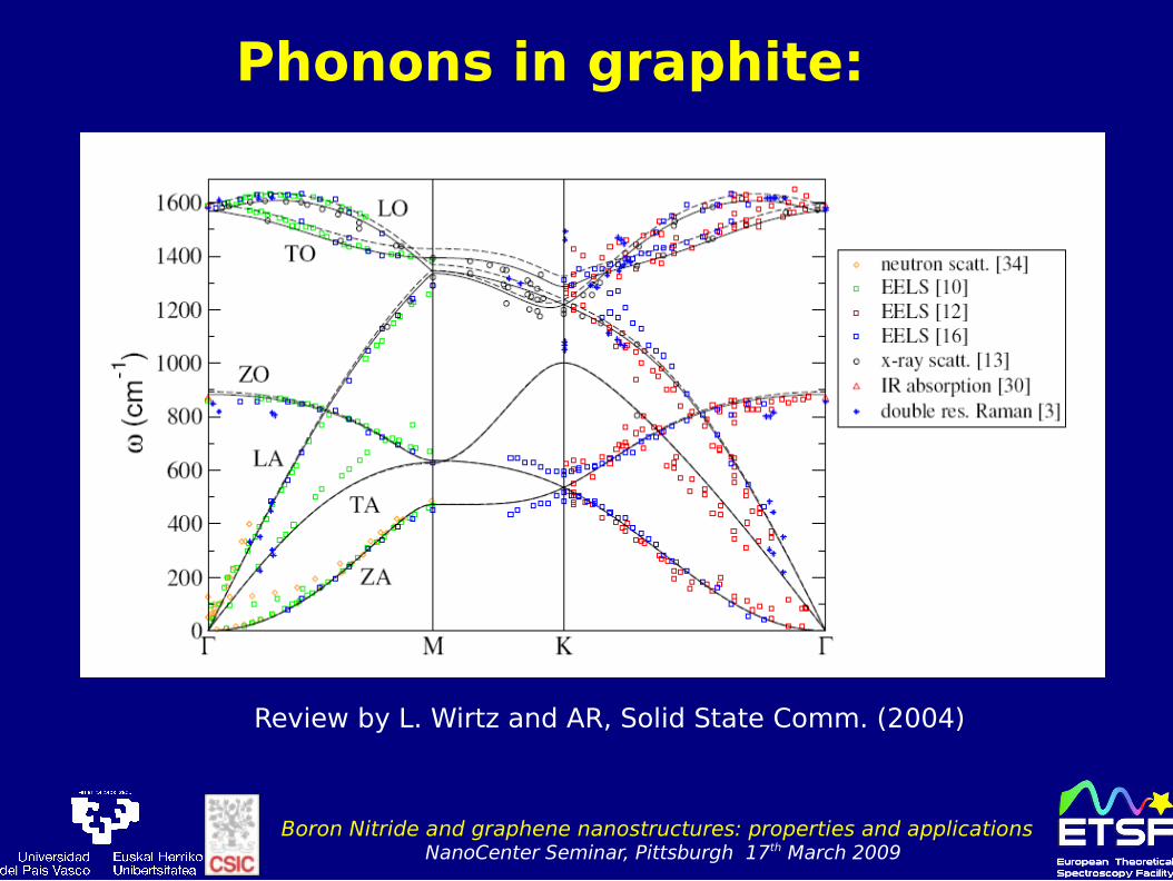
Phonons in graphite:
Review by L. Wirtz and AR, Solid State Comm. (2004)

Boron Nitride and graphene nanostructures: properties and applications NanoCenter Seminar, Pittsburgh 17th March 2009
Vibrational Properties: Raman and IR spectroscopy
PRL 98 (2007) (IXS experiments in Grenoble)

Boron Nitride and graphene nanostructures: properties and applications NanoCenter Seminar, Pittsburgh 17th March 2009
Electronic structure of BNtubes: (LDA)
Uniform band gap, no metallic BNtubes!
AR, X. Blase, M. L. Cohen, S. G. Louie PRB (1994,95); Euro. Phys. Lett (1994)
Boron Nitride and graphene nanostructures: properties and applications NanoCenter Seminar, Pittsburgh 17th March 2009
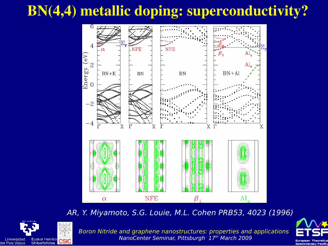
BN(4,4) metallic doping: superconductivity?
AR, Y. Miyamoto, S.G. Louie, M.L. Cohen PRB53, 4023 (1996)

Boron Nitride and graphene nanostructures: properties and applications NanoCenter Seminar, Pittsburgh 17th March 2009
The problem of Band Gap in nanotubesis related to the one of bulk hBN
How much is the band gap in hBN?
?
Boron Nitride and graphene nanostructures: properties and applications NanoCenter Seminar, Pittsburgh 17th March 2009

Boron Nitride and graphene nanostructures: properties and applications NanoCenter Seminar, Pittsburgh 17th March 2009
Optical Absorption/Emission Spectroscopy
x
optical gap ≠ photoemision (QP) gap
structural characterisation Role of packing: tubetube interaction

Boron Nitride and graphene nanostructures: properties and applications NanoCenter Seminar, Pittsburgh 17th March 2009
Beyond DFT
Bethe-Salpeter eqn:
Im [] ~ vc
|<v|D|c>|2 (Ec-E
v-)
Im [] ~ s |
vc<v|D|c>A
vcS|2 (S)

Boron Nitride and graphene nanostructures: properties and applications NanoCenter Seminar, Pittsburgh 17th March 2009
A.G. Marinopoulus, L. Reining, A. Rubio (unpublished 2002)
Optical Properties of CTubes: A way to elucidate tubechiralityZeolite type AlPo
4-5
N. Wang et al, Nature 408, 51 (2000)
CandidatesC(3,3)C(5,0)C(4,2)
Z.M..Lie et al, PRL (2001)
Depolarisationeffects
Marinopoulus, Reining, A.R. PRL /03), PEB(08)

Bound excitons in bulk h-BN
Experiment: Tarrio and Schnatterly, PRB 40, 7852 (1989) equally: Lauret et al PRL

Bound excitons in bulk h-BN
energy broadening: 0.1 eV

Fine structure of spectrum
B. Arnaud et al, PRL 96 (2006)Inset: comparison with absorption of K. Watanabe et al, Nature Materials (2004)
excitonic wave-functionhole on top of a N atom
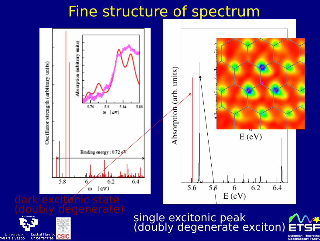
Fine structure of spectrum
single excitonic peak(doubly degenerate exciton)
dark excitonic state(doubly degenerate)

Boron Nitride and graphene nanostructures: properties and applications NanoCenter Seminar, Pittsburgh 17th March 2009
BN nanotubes Dimensionality effect: Exciton in (quasi-) 1-D, 2-D, 3-D
L. Wirtz, A. Marini, AR PRL (2006)
Depolarisation effects as in C tubes
Boron Nitride and graphene nanostructures: properties and applications NanoCenter Seminar, Pittsburgh 17th March 2009
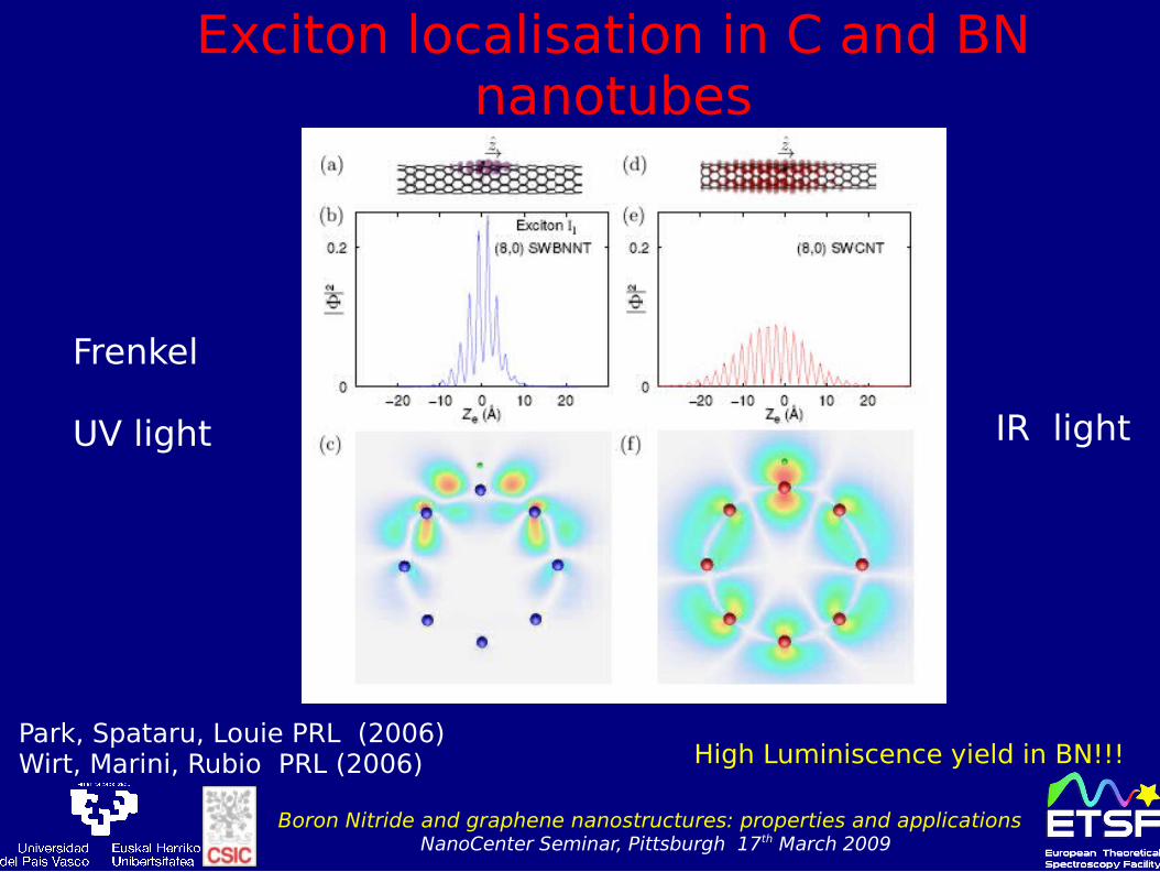
Park, Spataru, Louie PRL (2006)Wirt, Marini, Rubio PRL (2006)
Exciton localisation in C and BN nanotubes
Frenkel
UV light
High Luminiscence yield in BN!!!
IR light

Boron Nitride and graphene nanostructures: properties and applications NanoCenter Seminar, Pittsburgh 17th March 2009
Is there any experimental evidence of
such large excitonic effects?

Boron Nitride and graphene nanostructures: properties and applications NanoCenter Seminar, Pittsburgh 17th March 2009
e
EELS experiments on isolated BN nanotubes
Boron Nitride and graphene nanostructures: properties and applications NanoCenter Seminar, Pittsburgh 17th March 2009
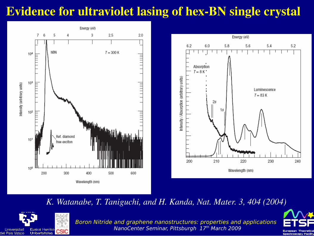
Evidence for ultraviolet lasing of hexBN single crystal
K. Watanabe, T. Taniguchi, and H. Kanda, Nat. Mater. 3, 404 (2004)
Boron Nitride and graphene nanostructures: properties and applications NanoCenter Seminar, Pittsburgh 17th March 2009
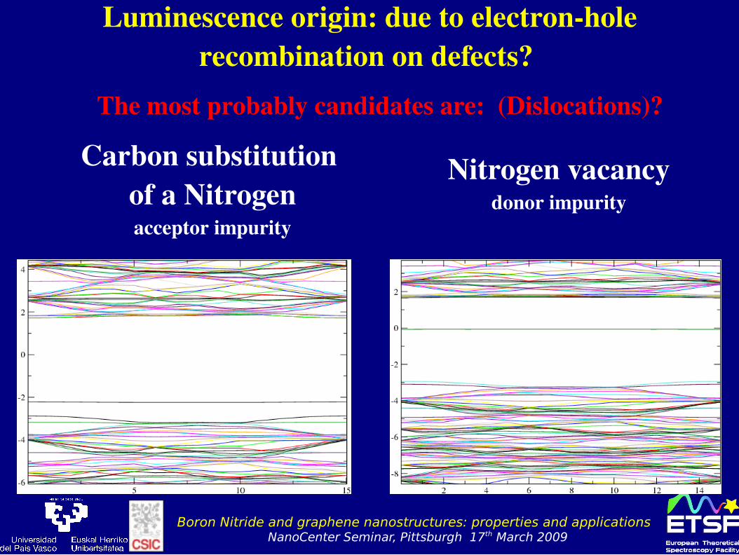
Luminescence origin: due to electronholerecombination on defects?
Carbon substitution of a Nitrogenacceptor impurity
The most probably candidates are: (Dislocations)?
Nitrogen vacancydonor impurity

Boron Nitride and graphene nanostructures: properties and applications NanoCenter Seminar, Pittsburgh 17th March 2009
The problem:valence and conduction orbitals are strongly modified
by the presence of an impurity
4
The highest three occupied orbitalsin the pure sheet (right) and with a carbon impurity in a 6x6 supercell

Boron Nitride and graphene nanostructures: properties and applications NanoCenter Seminar, Pittsburgh 17th March 2009
A high concentration of defects modifies the exciton peak in the single hex BN layer
Optical absorption within BSE approximation
GAP
6.1 eV
Optical absorption within RPA approximation
Defects/exciton states (shallow and deep) dominate the luminiscence below 6 eV; The main absorption peak of BN is at 6.1 eV ( this provides a coherent description of EELS , optics and luminescence)
Main absorption peak

Boron Nitride and graphene nanostructures: properties and applications NanoCenter Seminar, Pittsburgh 17th March 2009
Towards optoelectronic devices: role of
perpendicular E-field
ROLE of DEFECTS?
C. Attacalite, L. Wirtz, A. Marini and AR (in progress)

Boron Nitride and graphene nanostructures: properties and applications NanoCenter Seminar, Pittsburgh 17th March 2009

Boron Nitride and graphene nanostructures: properties and applications NanoCenter Seminar, Pittsburgh 17th March 2009
No control of absorption/luminescence in Pure BN tubes
Boron Nitride and graphene nanostructures: properties and applications NanoCenter Seminar, Pittsburgh 17th March 2009
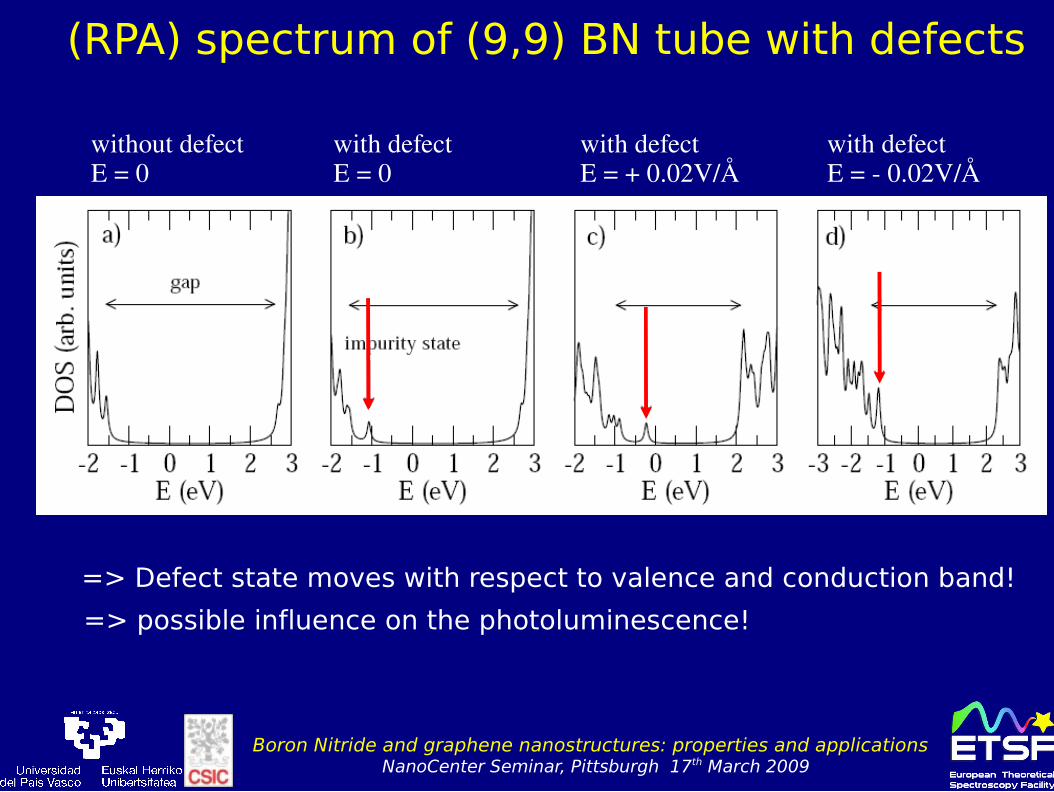
(RPA) spectrum of (9,9) BN tube with defects
with defectE = + 0.02V/Å
with defectE = 0.02V/Å
with defectE = 0
without defectE = 0
=> Defect state moves with respect to valence and conduction band!
=> possible influence on the photoluminescence!

Boron Nitride and graphene nanostructures: properties and applications NanoCenter Seminar, Pittsburgh 17th March 2009
Transverse Electric Field in BN: control blue/UV Light emission ?
Through Defects

Boron Nitride and graphene nanostructures: properties and applications NanoCenter Seminar, Pittsburgh 17th March 2009
GRAPHITE / GRAPHENE
recent work on ARPES, correlation effects and
electron-phonon coupling
Exp (T.Pichler group, U Wien, Austria)
D. C. Elias et al., Science 323, 610 -613 (2009)
Ongoing work:optics of hydrogenated graphene: graphAne
GAP ~ 5.4 eV

Boron Nitride and graphene nanostructures: properties and applications NanoCenter Seminar, Pittsburgh 17th March 2009
Electron-electron correlations

Boron Nitride and graphene nanostructures: properties and applications NanoCenter Seminar, Pittsburgh 17th March 2009
Electron-electron and e-phonon coupling

Boron Nitride and graphene nanostructures: properties and applications NanoCenter Seminar, Pittsburgh 17th March 2009
Electron-electron and e-phonon coupling
Boron Nitride and graphene nanostructures: properties and applications NanoCenter Seminar, Pittsburgh 17th March 2009
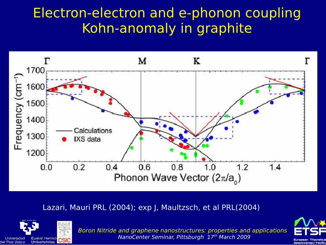
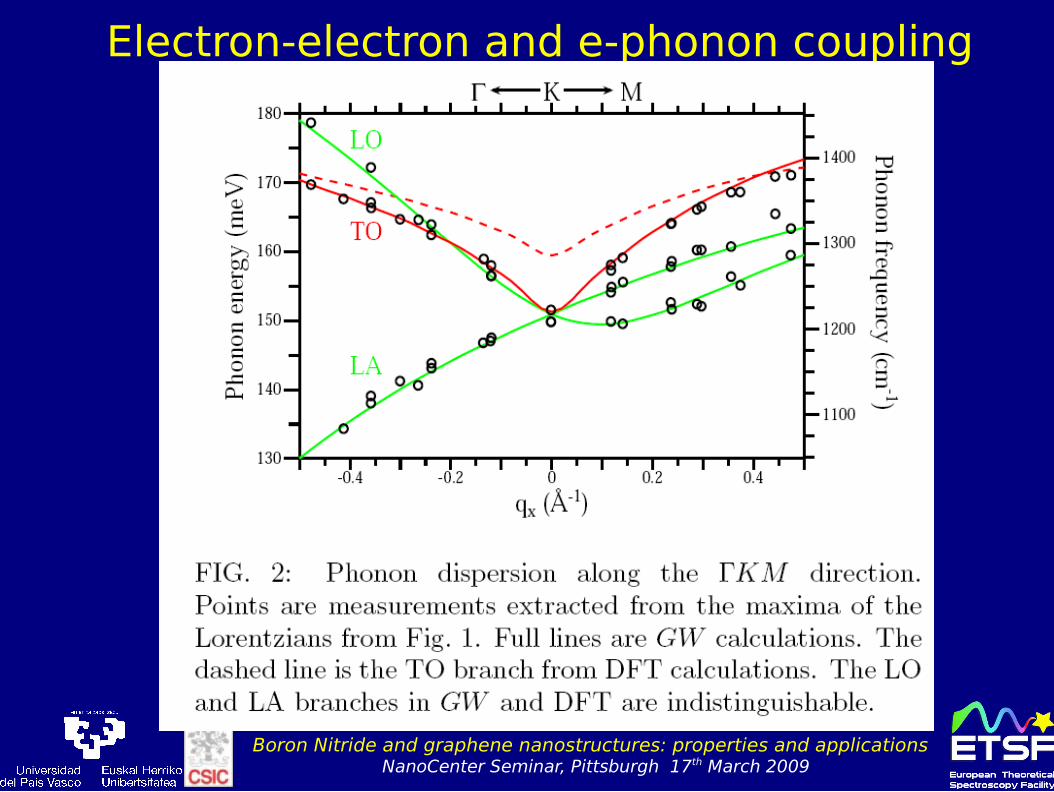
Electron-electron and e-phonon couplingKohn-anomaly in graphite
Lazari, Mauri PRL (2004); exp J, Maultzsch, et al PRL(2004)

Boron Nitride and graphene nanostructures: properties and applications NanoCenter Seminar, Pittsburgh 17th March 2009
Phonon dispersion close to KIn spite of the general good agreement the
situation is not clear close to KK

Boron Nitride and graphene nanostructures: properties and applications NanoCenter Seminar, Pittsburgh 17th March 2009
Phonon dispersion close to K
Boron Nitride and graphene nanostructures: properties and applications NanoCenter Seminar, Pittsburgh 17th March 2009
Electron-electron and e-phonon coupling

Boron Nitride and graphene nanostructures: properties and applications NanoCenter Seminar, Pittsburgh 17th March 2009
K K'
{ℏq
{
q
Raman Dline
dispersive

Boron Nitride and graphene nanostructures: properties and applications NanoCenter Seminar, Pittsburgh 17th March 2009
Raman Dline
Boron Nitride and graphene nanostructures: properties and applications NanoCenter Seminar, Pittsburgh 17th March 2009
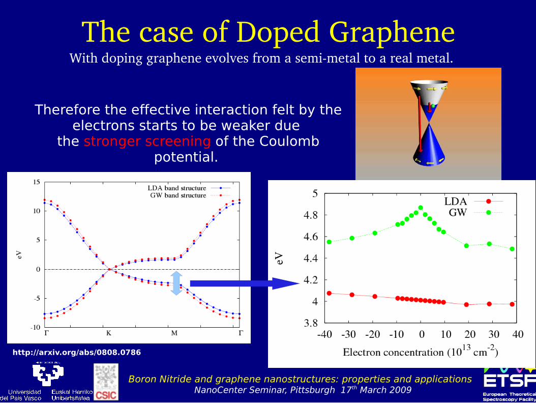
The case of Doped Graphene
Therefore the effective interaction felt by the electrons starts to be weaker due
the stronger screening of the Coulomb potential.
With doping graphene evolves from a semimetal to a real metal.
http://arxiv.org/abs/0808.0786

Boron Nitride and graphene nanostructures: properties and applications NanoCenter Seminar, Pittsburgh 17th March 2009
Electronphonon Coupling at KLDA results is recovered in doping graphene

Boron Nitride and graphene nanostructures: properties and applications NanoCenter Seminar, Pittsburgh 17th March 2009
Summary ●BN alternative material to C tubes for nanoelectronic applications
●Compatible with C; add to the nano-lego
●Optical-devices: luminiscence tunable by the applied perpendicular E-field (high efficiency); excitonic effects important
●Work on chemical synthesis: large scale production
MORE to come in the near future..................

Boron Nitride and graphene nanostructures: properties and applications NanoCenter Seminar, Pittsburgh 17th March 2009
Acknowledgements
http://www.etsf.es
S.G. Louie, M.L. Cohen and A. Zettl, Y. Miyamoto (NEC)Department of Physics, University of California at Berkeley, USA
Andrea MariniIstituto Nazionale per la Fisica della Materia e Dipartimento di Fisica
dell'Università di Roma ``Tor Vergata'', Roma, Italy
Ludger Wirtz, Francesco Mauri and Claudio Attacalite
CNRS, France
J. Serrano (ESRF Grenoble) T. Pichler (IW F Dresden)

Boron Nitride and graphene nanostructures: properties and applications NanoCenter Seminar, Pittsburgh 17th March 2009
For more details see: http://nano-bio.ehu.es
Than
k yo
u!!!!

Boron Nitride and graphene nanostructures: properties and applications NanoCenter Seminar, Pittsburgh 17th March 2009