LMX9830 Bluetooth® Serial Port Module - Texas … Bluetooth® Serial Port Module 1 Features 3...
56
Product Folder Sample & Buy Technical Documents Tools & Software Support & Community LMX9830 SNOSAU0C – MAY 2008 – REVISED JUNE 2015 LMX9830 Bluetooth® Serial Port Module 1 Features 3 Description The Texas Instruments LMX9830 Bluetooth Serial 1• Compliant With the Bluetooth ® 2.0 Core Port module is a highly integrated Bluetooth 2.0 Specification baseband controller and 2.4-GHz radio, combined to – Qualified Design ID (PRD 2.0): B012364 form a complete small form factor (6.1 mm × 9.1 mm • Input Sensitivity Better than –80 dBm × 1.2 mm) Bluetooth node. • Class 2 Operation All hardware and firmware is included to provide a complete solution from antenna through the complete • Low Power Consumption lower and upper layers of the Bluetooth stack, up to • High Integration: the application including the Generic Access Profile – Implemented in 0.18-μm CMOS Technology (GAP), the Service Discovery Application Profile – RF Includes Antenna Filter and Switch On- (SDAP), and the Serial Port Profile (SPP). The module includes a configurable service database to Chip fulfill service requests for additional profiles on the host. Moreover, the LMX9830 is prequalified as a 2 Applications Bluetooth Integrated Component. Conformance • Personal Digital Assistants testing through the Bluetooth qualification program. • POS Terminals The LMX9830 enables a short time to market after system integration by ensuring a high probability of • Data Logging Systems compliance and interoperability. • Audio Gateway Applications Based on TI's CompactRISC 16-bit processor • Telemedicine/Medical, Industrial and Scientific architecture and Digital Smart Radio technology, the LMX9830 is optimized to handle the data and link management processing requirements of a Bluetooth node. Device Information (1) PART NUMBER PACKAGE BODY SIZE (NOM) LMX9830 NFBGA (60) 9.00 mm × 6.00 mm (1) For all available packages, see the orderable addendum at the end of the data sheet. 4 Block Diagram 1 An IMPORTANT NOTICE at the end of this data sheet addresses availability, warranty, changes, use in safety-critical applications, intellectual property matters and other important disclaimers. PRODUCTION DATA.
-
Upload
dangkhuong -
Category
Documents
-
view
224 -
download
0
Transcript of LMX9830 Bluetooth® Serial Port Module - Texas … Bluetooth® Serial Port Module 1 Features 3...

Product
Folder
Sample &Buy
Technical
Documents
Tools &
Software
Support &Community
LMX9830SNOSAU0C –MAY 2008–REVISED JUNE 2015
LMX9830 Bluetooth® Serial Port Module1 Features 3 Description
The Texas Instruments LMX9830 Bluetooth Serial1• Compliant With the Bluetooth® 2.0 Core
Port module is a highly integrated Bluetooth 2.0Specificationbaseband controller and 2.4-GHz radio, combined to
– Qualified Design ID (PRD 2.0): B012364 form a complete small form factor (6.1 mm × 9.1 mm• Input Sensitivity Better than –80 dBm × 1.2 mm) Bluetooth node.• Class 2 Operation All hardware and firmware is included to provide a
complete solution from antenna through the complete• Low Power Consumptionlower and upper layers of the Bluetooth stack, up to• High Integration:the application including the Generic Access Profile
– Implemented in 0.18-μm CMOS Technology (GAP), the Service Discovery Application Profile– RF Includes Antenna Filter and Switch On- (SDAP), and the Serial Port Profile (SPP). The
module includes a configurable service database toChipfulfill service requests for additional profiles on thehost. Moreover, the LMX9830 is prequalified as a2 ApplicationsBluetooth Integrated Component. Conformance
• Personal Digital Assistants testing through the Bluetooth qualification program.• POS Terminals The LMX9830 enables a short time to market after
system integration by ensuring a high probability of• Data Logging Systemscompliance and interoperability.• Audio Gateway ApplicationsBased on TI's CompactRISC 16-bit processor• Telemedicine/Medical, Industrial and Scientificarchitecture and Digital Smart Radio technology, theLMX9830 is optimized to handle the data and linkmanagement processing requirements of a Bluetoothnode.
Device Information(1)
PART NUMBER PACKAGE BODY SIZE (NOM)LMX9830 NFBGA (60) 9.00 mm × 6.00 mm
(1) For all available packages, see the orderable addendum atthe end of the data sheet.
4 Block Diagram
1
An IMPORTANT NOTICE at the end of this data sheet addresses availability, warranty, changes, use in safety-critical applications,intellectual property matters and other important disclaimers. PRODUCTION DATA.

LMX9830SNOSAU0C –MAY 2008–REVISED JUNE 2015 www.ti.com
Table of Contents1 Features .................................................................. 1 9 Detailed Description ............................................ 10
9.1 Overview ................................................................. 102 Applications ........................................................... 19.2 Functional Block Diagram ....................................... 103 Description ............................................................. 19.3 Feature Description................................................. 104 Block Diagram........................................................ 19.4 Device Functional Modes........................................ 365 Revision History..................................................... 2
10 Application and Implementation........................ 416 Pin Configuration and Functions ......................... 310.1 Typical Application ................................................ 417 Specifications......................................................... 510.2 System Examples ................................................. 447.1 Absolute Maximum Ratings ...................................... 5
11 Power Supply Recommendations ..................... 477.2 ESD Ratings.............................................................. 511.1 Filtered Power Supply........................................... 477.3 Recommended Operating Conditions....................... 5
12 Device and Documentation Support ................. 507.4 Thermal Information .................................................. 612.1 Device Support...................................................... 507.5 Power Supply Requirements .................................... 612.2 Documentation Support ........................................ 507.6 Digital DC Characteristics ......................................... 612.3 Community Resources.......................................... 507.7 RF Receiver Performance Characteristics................ 712.4 Trademarks ........................................................... 507.8 RF Transmitter Performance Characteristics............ 712.5 Electrostatic Discharge Caution............................ 507.9 RF Synthesizer Performance Characteristics ........... 812.6 Glossary ................................................................ 507.10 Typical Characteristics ............................................ 8
13 Mechanical, Packaging, and Orderable8 Parameter Measurement Information .................. 9Information ........................................................... 50
5 Revision HistoryNOTE: Page numbers for previous revisions may differ from page numbers in the current version.
Changes from Revision B (April 2013) to Revision C Page
• Added ESD Ratings table, Feature Description section, Device Functional Modes, Application and Implementationsection, Power Supply Recommendations section, Layout section, Device and Documentation Support section, andMechanical, Packaging, and Orderable Information section .................................................................................................. 1
Changes from Revision A (April 2013) to Revision B Page
• Changed layout of National Data Sheet to TI format ............................................................................................................. 1
2 Submit Documentation Feedback Copyright © 2008–2015, Texas Instruments Incorporated
Product Folder Links: LMX9830

LMX9830www.ti.com SNOSAU0C –MAY 2008–REVISED JUNE 2015
6 Pin Configuration and Functions
NZB Package60-Pin NFBGA
Top View
Pin FunctionsPAD NAME PAD LOCATION TYPE DEFAULT LAYOUT DESCRIPTION
ANT D10 I/O — RF Antenna 50 Ω Nominal ImpedanceB_RESET_RA# B6 O NC Buffered Reset Radio Output (active low)CTS# (1) C2 I GND (if not used) Host Serial Port Clear To Send (active low)ENV1# ENV1: Environment Select (active low) used forC6 I NC manufacturing test onlyGND B2,E2 — — GroundGND_IF D7 — — GroundGND_RF B9, C10, E10 — — GroundGND_VCO E9 — — GroundMDODI (2) D1 I/O — SPI Master Out Slave InNC A1,A2,A3 — NC Treat as no connect. Place pad for mechanical stabilityOP3/MWCS# OP3: Pin checked during Start-up Sequence forSee Table 8 andD3 I configuration optionTable 9 MWCS#: SPI Slave Select Input (active low)OP4/PG4 OP4: Pin checked during Start-up Sequence forOP4: I See Table 8 andD6 configuration optionPG4: I/O Table 9 PG4: GPIOOP5 See Table 8 and OP5: Pin checked during Start-up Sequence forF4 I/O Table 9 configuration optionOP6/SCL/MSK OP6: Pin checked during Start-up Sequence for
OP6: I configuration optionC1 See Table 8SCL/MSK: I/O SCL: ACCESS.Bus ClockMSK: SPI Shift
OP7/SDA/MDIDO OP7: Pin checked during Start-up Sequence forOP7: I configuration optionD4 See Table 8SDA/MDIDO: I/O SDA: ACCESS.Bus Serial Data
MDIDO: SPI Master In Slave OutPG6 A7 I/O — GPIOPG7 D2 I/O — GPIO - Default setup RF traffic LED indication
(1) Connect to GND if CTS is not use.(2) Must use 1-kΩ pullup.
Copyright © 2008–2015, Texas Instruments Incorporated Submit Documentation Feedback 3
Product Folder Links: LMX9830

LMX9830SNOSAU0C –MAY 2008–REVISED JUNE 2015 www.ti.com
Pin Functions (continued)PAD NAME PAD LOCATION TYPE DEFAULT LAYOUT DESCRIPTION
RDY# A4 O NC JTAG Ready Output (active low)RESET_BB# B7 I Baseband Reset (active low)RESET_RA# B8 I Radio Reset (active low)RTS# (3) B1 O NC (if not used) Host Serial Port Request To Send (active low)RXD B3 I — Host Serial Port Receive DataSCLK F1 I/O — Audio PCM Interface ClockSFS F2 I/O — Audio PCM Interface Frame SynchronizationSRD F3 I — Audio PCM Interface Receive Data InputSTD E3 O — Audio PCM Interface Transmit Data OutputTCK B4 I NC JTAG Test Clock InputTDI B5 I NC JTAG Test Data InputTDO D5 O NC JTAG Test Data OutputTE A9 I GND Test Enable - Used for manufacturing test onlyTMS A5 I NC JTAG Test Mode Select InputTST1/DIV2# TST1: Test Mode. Leave not connected to permit use
B10 I NC with VTune automatic tuning algorithmDIV2#: No longer supported
TST2 C7 I GND Test Mode, Connect to GNDTST3 C8 I GND Test Mode, Connect to GNDTST4 C9 I GND Test Mode, Connect to GNDTST5 D8 I GND Test Mode, Connect to GNDTST6 Test Input,
D9 I VCO_OUT Connect to VCO_OUT via 0-Ω resistor to permit usewith VTune automatic tuning algorithm
TXD C3 O — Host Serial Port Transmit DataX1_CKI E7 I — Crystal or External Clock 10-20 MHzX1_CKO F7 O — Crystal 10-20 MHzX2_CKI GNDF5 I 32.768-kHz Crystal Oscillator(if not used)X2_CKO NCE5 O 32.768-kHz Crystal Oscillator(if not used)XOSCEN Clock Request. Toggles with X2 (LP0) crystalA6 O — enable/disableVCC E1 I — Voltage Regulator InputVCC_CORE C5 O — 1.8-V Voltage Regulator OutputVCC_IO C4 I — Power Supply I/OVCC_IOP E4 I — Power Supply Audio InterfaceVCC_PLL F6 O — 1.8-V Core Logic Power Supply OutputVCO_IN F9 I — VCO Tuning Input, feedback from Loop filterVCO_OUT F8 O — Charge Pump Output, connect to Loop filterVDD_IF A8 I — Power Supply IFVDD_IOR E6 I — Power Supply I/O Radio/BBVDD_RF A10 I — Power Supply RFVDD_VCO F10 I — Power Supply VCOVDD_X1 E8 I — Power Supply Crystal Oscillator
(3) Treat as No Connect if RTS is not used. Pad required for mechanical stability.
4 Submit Documentation Feedback Copyright © 2008–2015, Texas Instruments Incorporated
Product Folder Links: LMX9830
LMX9830www.ti.com SNOSAU0C –MAY 2008–REVISED JUNE 2015
7 Specifications
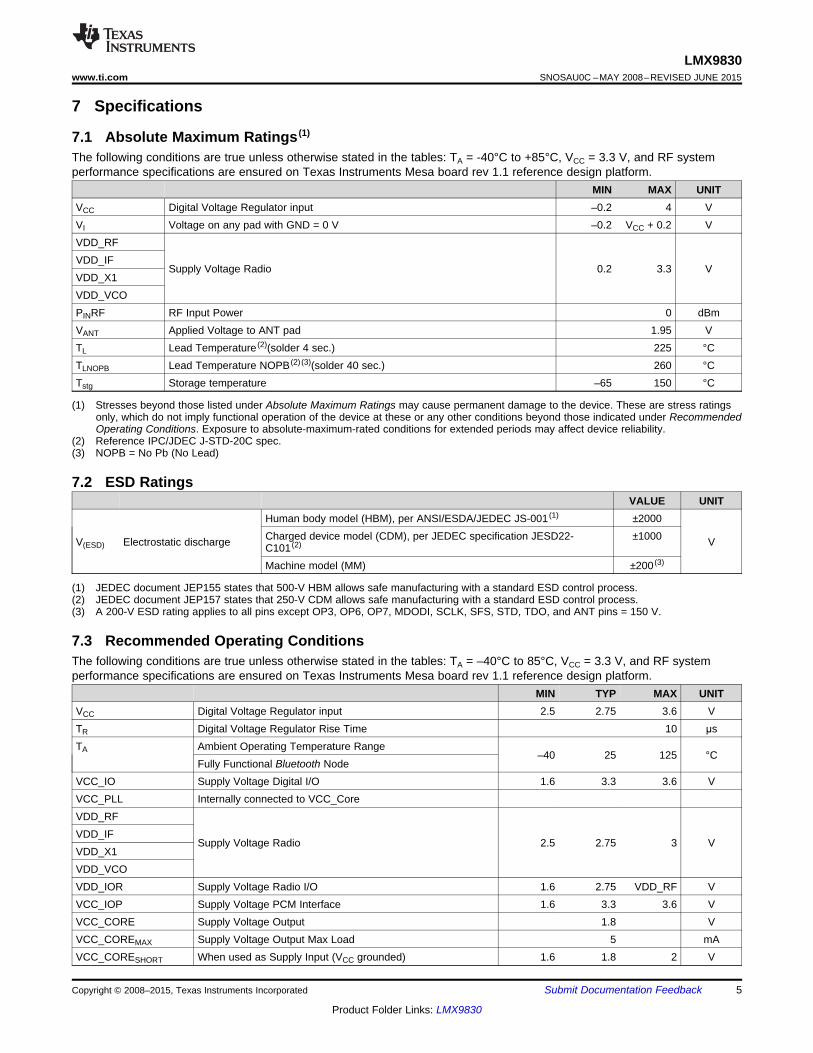
7.1 Absolute Maximum Ratings (1)
The following conditions are true unless otherwise stated in the tables: TA = -40°C to +85°C, VCC = 3.3 V, and RF systemperformance specifications are ensured on Texas Instruments Mesa board rev 1.1 reference design platform.
MIN MAX UNITVCC Digital Voltage Regulator input –0.2 4 VVI Voltage on any pad with GND = 0 V –0.2 VCC + 0.2 VVDD_RFVDD_IF
Supply Voltage Radio 0.2 3.3 VVDD_X1VDD_VCOPINRF RF Input Power 0 dBmVANT Applied Voltage to ANT pad 1.95 VTL Lead Temperature (2)(solder 4 sec.) 225 °CTLNOPB Lead Temperature NOPB (2) (3)(solder 40 sec.) 260 °CTstg Storage temperature –65 150 °C
(1) Stresses beyond those listed under Absolute Maximum Ratings may cause permanent damage to the device. These are stress ratingsonly, which do not imply functional operation of the device at these or any other conditions beyond those indicated under RecommendedOperating Conditions. Exposure to absolute-maximum-rated conditions for extended periods may affect device reliability.
(2) Reference IPC/JDEC J-STD-20C spec.(3) NOPB = No Pb (No Lead)
7.2 ESD RatingsVALUE UNIT
Human body model (HBM), per ANSI/ESDA/JEDEC JS-001 (1) ±2000Charged device model (CDM), per JEDEC specification JESD22- ±1000V(ESD) Electrostatic discharge VC101 (2)
Machine model (MM) ±200 (3)
(1) JEDEC document JEP155 states that 500-V HBM allows safe manufacturing with a standard ESD control process.(2) JEDEC document JEP157 states that 250-V CDM allows safe manufacturing with a standard ESD control process.(3) A 200-V ESD rating applies to all pins except OP3, OP6, OP7, MDODI, SCLK, SFS, STD, TDO, and ANT pins = 150 V.
7.3 Recommended Operating ConditionsThe following conditions are true unless otherwise stated in the tables: TA = –40°C to 85°C, VCC = 3.3 V, and RF systemperformance specifications are ensured on Texas Instruments Mesa board rev 1.1 reference design platform.
MIN TYP MAX UNITVCC Digital Voltage Regulator input 2.5 2.75 3.6 VTR Digital Voltage Regulator Rise Time 10 μsTA Ambient Operating Temperature Range
–40 25 125 °CFully Functional Bluetooth Node
VCC_IO Supply Voltage Digital I/O 1.6 3.3 3.6 VVCC_PLL Internally connected to VCC_CoreVDD_RFVDD_IF
Supply Voltage Radio 2.5 2.75 3 VVDD_X1VDD_VCOVDD_IOR Supply Voltage Radio I/O 1.6 2.75 VDD_RF VVCC_IOP Supply Voltage PCM Interface 1.6 3.3 3.6 VVCC_CORE Supply Voltage Output 1.8 VVCC_COREMAX Supply Voltage Output Max Load 5 mAVCC_CORESHORT When used as Supply Input (VCC grounded) 1.6 1.8 2 V
Copyright © 2008–2015, Texas Instruments Incorporated Submit Documentation Feedback 5
Product Folder Links: LMX9830
LMX9830SNOSAU0C –MAY 2008–REVISED JUNE 2015 www.ti.com
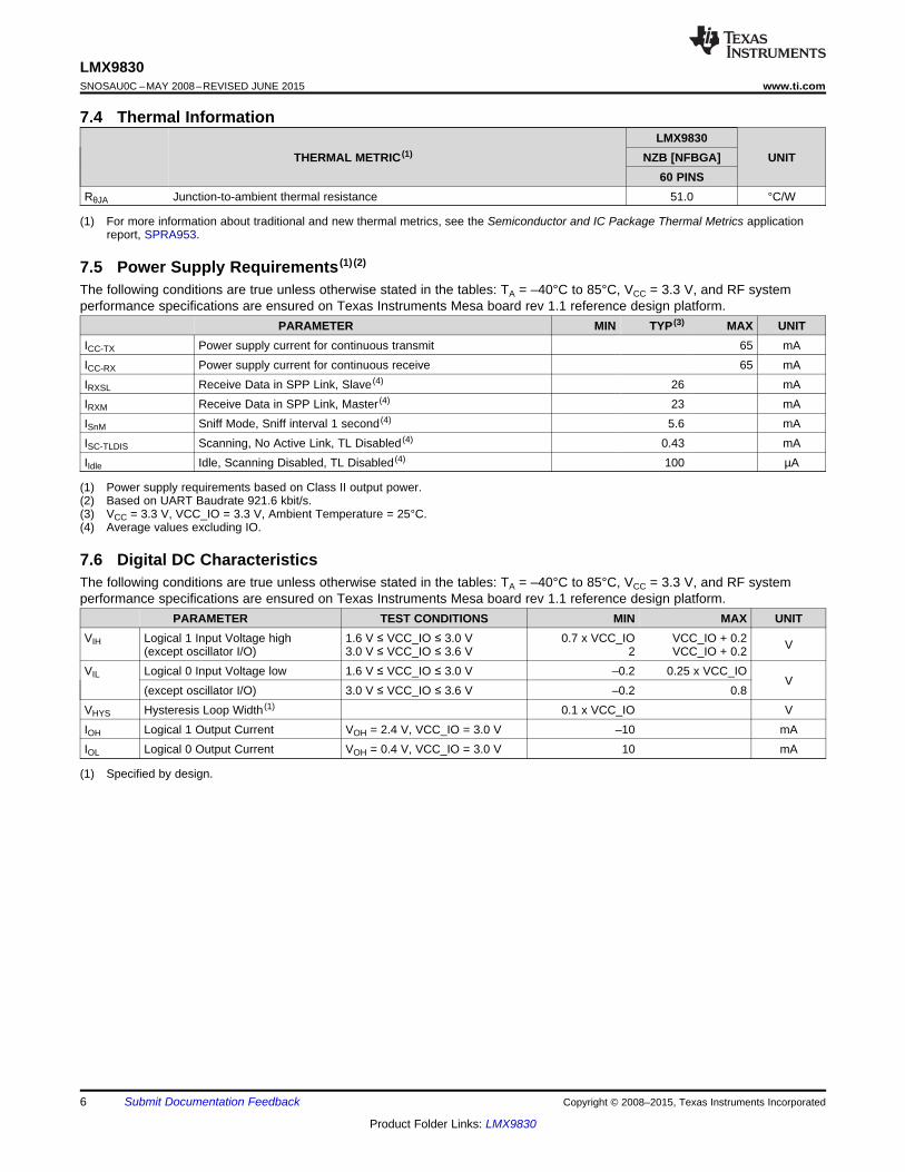
7.4 Thermal InformationLMX9830
THERMAL METRIC (1) NZB [NFBGA] UNIT60 PINS
RθJA Junction-to-ambient thermal resistance 51.0 °C/W
(1) For more information about traditional and new thermal metrics, see the Semiconductor and IC Package Thermal Metrics applicationreport, SPRA953.
7.5 Power Supply Requirements (1) (2)
The following conditions are true unless otherwise stated in the tables: TA = –40°C to 85°C, VCC = 3.3 V, and RF systemperformance specifications are ensured on Texas Instruments Mesa board rev 1.1 reference design platform.
PARAMETER MIN TYP (3) MAX UNITICC-TX Power supply current for continuous transmit 65 mAICC-RX Power supply current for continuous receive 65 mAIRXSL Receive Data in SPP Link, Slave (4) 26 mAIRXM Receive Data in SPP Link, Master (4) 23 mAISnM Sniff Mode, Sniff interval 1 second (4) 5.6 mAISC-TLDIS Scanning, No Active Link, TL Disabled (4) 0.43 mAIIdle Idle, Scanning Disabled, TL Disabled (4) 100 µA
(1) Power supply requirements based on Class II output power.(2) Based on UART Baudrate 921.6 kbit/s.(3) VCC = 3.3 V, VCC_IO = 3.3 V, Ambient Temperature = 25°C.(4) Average values excluding IO.
7.6 Digital DC CharacteristicsThe following conditions are true unless otherwise stated in the tables: TA = –40°C to 85°C, VCC = 3.3 V, and RF systemperformance specifications are ensured on Texas Instruments Mesa board rev 1.1 reference design platform.
PARAMETER TEST CONDITIONS MIN MAX UNITVIH Logical 1 Input Voltage high 1.6 V ≤ VCC_IO ≤ 3.0 V 0.7 x VCC_IO VCC_IO + 0.2 V(except oscillator I/O) 3.0 V ≤ VCC_IO ≤ 3.6 V 2 VCC_IO + 0.2VIL Logical 0 Input Voltage low 1.6 V ≤ VCC_IO ≤ 3.0 V –0.2 0.25 x VCC_IO
V(except oscillator I/O) 3.0 V ≤ VCC_IO ≤ 3.6 V –0.2 0.8
VHYS Hysteresis Loop Width (1) 0.1 x VCC_IO VIOH Logical 1 Output Current VOH = 2.4 V, VCC_IO = 3.0 V –10 mAIOL Logical 0 Output Current VOH = 0.4 V, VCC_IO = 3.0 V 10 mA
(1) Specified by design.
6 Submit Documentation Feedback Copyright © 2008–2015, Texas Instruments Incorporated
Product Folder Links: LMX9830
LMX9830www.ti.com SNOSAU0C –MAY 2008–REVISED JUNE 2015
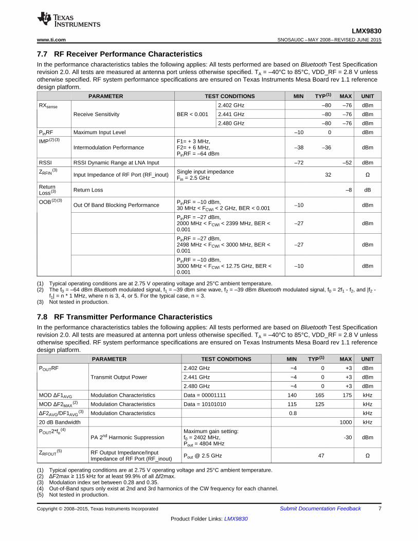
7.7 RF Receiver Performance CharacteristicsIn the performance characteristics tables the following applies: All tests performed are based on Bluetooth Test Specificationrevision 2.0. All tests are measured at antenna port unless otherwise specified. TA = –40°C to 85°C, VDD_RF = 2.8 V unlessotherwise specified. RF system performance specifications are ensured on Texas Instruments Mesa Board rev 1.1 referencedesign platform.
PARAMETER TEST CONDITIONS MIN TYP (1) MAX UNITRXsense 2.402 GHz –80 –76 dBm
Receive Sensitivity BER < 0.001 2.441 GHz –80 –76 dBm2.480 GHz –80 –76 dBm
PinRF Maximum Input Level –10 0 dBmIMP (2) (3) F1= + 3 MHz,
Intermodulation Performance F2= + 6 MHz, –38 –36 dBmPinRF = –64 dBm
RSSI RSSI Dynamic Range at LNA Input –72 –52 dBmZRFIN
(3) Single input impedanceInput Impedance of RF Port (RF_inout) 32 ΩFin = 2.5 GHzReturn Return Loss –8 dBLoss (3)
OOB (2) (3) PinRF = –10 dBm,Out Of Band Blocking Performance –10 dBm30 MHz < FCWI < 2 GHz, BER < 0.001PinRF = –27 dBm,2000 MHz < FCWI < 2399 MHz, BER < –27 dBm0.001PinRF = –27 dBm,2498 MHz < FCWI < 3000 MHz, BER < –27 dBm0.001PinRF = –10 dBm,3000 MHz < FCWI < 12.75 GHz, BER < –10 dBm0.001
(1) Typical operating conditions are at 2.75 V operating voltage and 25°C ambient temperature.(2) The f0 = –64 dBm Bluetooth modulated signal, f1 = –39 dbm sine wave, f2 = –39 dBm Bluetooth modulated signal, f0 = 2f1 - f2, and |f2 -
f1| = n * 1 MHz, where n is 3, 4, or 5. For the typical case, n = 3.(3) Not tested in production.
7.8 RF Transmitter Performance CharacteristicsIn the performance characteristics tables the following applies: All tests performed are based on Bluetooth Test Specificationrevision 2.0. All tests are measured at antenna port unless otherwise specified. TA = –40°C to 85°C, VDD_RF = 2.8 V unlessotherwise specified. RF system performance specifications are ensured on Texas Instruments Mesa Board rev 1.1 referencedesign platform.
PARAMETER TEST CONDITIONS MIN TYP (1) MAX UNITPOUTRF 2.402 GHz −4 0 +3 dBm
Transmit Output Power 2.441 GHz −4 0 +3 dBm2.480 GHz −4 0 +3 dBm
MOD ΔF1AVG Modulation Characteristics Data = 00001111 140 165 175 kHzMOD ΔF2MAX
(2) Modulation Characteristics Data = 10101010 115 125 kHzΔF2AVG/DF1AVG
(3) Modulation Characteristics 0.8 kHz20 dB Bandwidth 1000 kHzPOUT2*fo(4) Maximum gain setting:
PA 2nd Harmonic Suppression f0 = 2402 MHz, -30 dBmPout = 4804 MHz
ZRFOUT(5) RF Output Impedance/Input Pout @ 2.5 GHz 47 ΩImpedance of RF Port (RF_inout)
(1) Typical operating conditions are at 2.75 V operating voltage and 25°C ambient temperature.(2) ΔF2max ≥ 115 kHz for at least 99.9% of all Δf2max.(3) Modulation index set between 0.28 and 0.35.(4) Out-of-Band spurs only exist at 2nd and 3rd harmonics of the CW frequency for each channel.(5) Not tested in production.
Copyright © 2008–2015, Texas Instruments Incorporated Submit Documentation Feedback 7
Product Folder Links: LMX9830

LMX9830SNOSAU0C –MAY 2008–REVISED JUNE 2015 www.ti.com
7.9 RF Synthesizer Performance CharacteristicsIn the performance characteristics tables the following applies: All tests performed are based on Bluetooth Test Specificationrevision 2.0. All tests are measured at antenna port unless otherwise specified. TA = –40°C to 85°C, VDD_RF = 2.8 V unlessotherwise specified. RF system performance specifications are ensured on Texas Instruments Mesa Board rev 1.1 referencedesign platform.
PARAMETER TEST CONDITIONS MIN TYP MAX UNITfVCO VCO Frequency Range 2402 2480 MHztLOCK Lock Time f0 ± 20 kHz 120 µsΔf0offset (1) Initial Carrier Frequency Tolerance During preamble -75 0 75 kHzΔf0drift (1) DH1 data packet -25 0 25 kHz
DH3 data packet -40 0 40 kHzInitial Carrier Frequency Drift
DH5 data packet -40 0 40 kHzDrift Rate -20 0 20 kHz/50µs
tD - TX Transmitter Delay Time From TX data to antenna 4 µs
(1) Frequency accuracy is dependent on crystal oscillator chosen. The crystal must have a cumulative accuracy of < ±20 ppm to meetBluetooth specifications.
7.10 Typical Characteristics
Figure 1. Modulation Figure 2. Transmit Spectrum
Figure 3. Corresponding Eye Diagram Figure 4. Synthesizer Phase Noise
8 Submit Documentation Feedback Copyright © 2008–2015, Texas Instruments Incorporated
Product Folder Links: LMX9830

LMX9830www.ti.com SNOSAU0C –MAY 2008–REVISED JUNE 2015
8 Parameter Measurement Information
Figure 5. Front-End Bandpass Filter Response
Figure 6. TX and RX Pin 50-Ω Impedance Characteristics
Figure 7. Transceiver Return Loss
Copyright © 2008–2015, Texas Instruments Incorporated Submit Documentation Feedback 9
Product Folder Links: LMX9830

LMX9830SNOSAU0C –MAY 2008–REVISED JUNE 2015 www.ti.com
9 Detailed Description
9.1 OverviewLMX9830 is a highly compact Bluetooth 2.0 module solution, with integrated radio, controller, and processor. Thebuilt-in Bluetooth stacks up to the application layer allows users to communicate directly with SPP commands,and develop additional SPP-based Bluetooth profiles on Host through UART interface.
9.2 Functional Block Diagram
9.3 Feature Description
9.3.1 Feature OverviewThe firmware supplied in the on-chip ROM memory offers a complete Bluetooth (v2.0) stack including profilesand command interface. This firmware features point-to-point and point-to-multipoint link management supportingdata rates up to the theoretical maximum over RFComm of 704 kbps (Best in Class in the industry). The internalmemory supports up to 7 active Bluetooth data links and one active SCO link.
The on-chip Patch RAM provided for lowest cost and risk, allows the flexibility of a firmware upgrade.
The LMX9830 module is lead free and RoHS (Restriction of Hazardous Substances) compliant. For moreinformation on those quality standards, visit TI's green compliance website athttp://focus.ti.com/quality/docs/qualityhome.tsp
10 Submit Documentation Feedback Copyright © 2008–2015, Texas Instruments Incorporated
Product Folder Links: LMX9830

LMX9830www.ti.com SNOSAU0C –MAY 2008–REVISED JUNE 2015
Feature Description (continued)9.3.1.1 Hardware• Baseband and Link Management Processors• CompactRISC Core• Embedded ROM and Patch RAM Memory• UART Command/Data Port:
– Support for up to 921.6 k Baud Rate• Auxiliary Host Interface Ports:
– Link Status– Transceiver Status (TX or RX)– Three General Purpose I/Os, Available through the API– Alternative IO Functions:
– Link Status– Transport Layer Activity
• Advanced Power Management (APM) Features:– Advanced Power Management functions
• Advanced Audio Interface for External PCM Codec• ACCESS.Bus and SPI/Microwire for Interfacing with External Nonvolatile Memory
9.3.1.2 Firmware• Complete Bluetooth Stack including:
– Baseband and Link Manager– L2CAP, RFCOMM, SDP– Profiles:
– GAP– SDAP– SPP
• Additional Profile support on Host, for example:– Dial Up Networking (DUN)– Facsimile Profile (FAX)– File Transfer Protocol (FTP)– Object Push Profile (OPP)– Synchronization Profile (SYNC)– Headset (HSP)– Handsfree Profile (HFP)– Basic Imaging Profile (BIP)– Basic Printing Profile (BPP)
• On-Chip application including:– Default connections– Command Interface:
– Link setup and configuration (also Multipoint)– Configuration of the module– Service database modifications
– UART Transparent mode– Optimized cable replacement :
– Automatic transparent mode– Event filter
Copyright © 2008–2015, Texas Instruments Incorporated Submit Documentation Feedback 11
Product Folder Links: LMX9830

LMX9830SNOSAU0C –MAY 2008–REVISED JUNE 2015 www.ti.com
Feature Description (continued)9.3.1.3 Highly Integrated Digital Technology• Accepts external clock or crystal input:
– 13 MHz Typical– Supports 10 - 20 MHz– Secondary 32.768-kHz oscillator for low-power modes– 20 ppm cumulative clock error required for Bluetooth
• Synthesizer:– Integrated VCO– Provides all clocking for radio and baseband functions
• Antenna Port (50 Ω nominal impedance):– Embedded front-end filter for enhanced out of band performance
• Integrated transmit/receive switch (full duplex operation via antenna port)• Better than –80 dBm input sensitivity• 0 dBm typical output power
9.3.1.4 Physical• Compact size - 6.1 mm × 9.1 mm × 1.2 mm• Complete system interface provided in Ball Grid Array on underside for surface mount assembly
9.3.2 Baseband and Link Management ProcessorsBaseband and Lower Link control functions are implemented using a combination of TI's CompactRISC 16-bitprocessor and the Bluetooth Lower Link Controller. These processors operate from integrated ROM memory andRAM and execute on-board firmware implementing all Bluetooth functions.
9.3.2.1 Bluetooth Lower Link ControllerThe integrated Bluetooth Lower Link Controller (LLC) complies with the Bluetooth Specification version 2.0 andimplements the following functions:• Adaptive Frequency Hopping• Interlaced Scanning• Fast Connect• Support for 1, 3, and 5 slot packet types• 79 Channel hop frequency generation circuitry• Fast frequency hopping at 1600 hops per second• Power management control• Access code correlation and slot timing recovery
9.3.2.2 Bluetooth Upper Layer StackThe integrated upper layer stack is prequalified and includes the following protocol layers:• L2CAP• RFComm• SDP
9.3.2.3 Profile SupportThe on-chip application of the LMX9830 allows full stand-alone operation, without any Bluetooth protocol layernecessary outside the module. It supports the Generic Access Profile (GAP), the Service Discovery ApplicationProfile (SDAP), and the Serial Port Profile (SPP).
The on-chip profiles can be used as interfaces to additional profiles executed on the host. The LMX9830 includesa configurable service database to answer requests with the profiles supported.
12 Submit Documentation Feedback Copyright © 2008–2015, Texas Instruments Incorporated
Product Folder Links: LMX9830

LMX9830www.ti.com SNOSAU0C –MAY 2008–REVISED JUNE 2015
Feature Description (continued)9.3.2.4 Application With Command InterfaceThe module supports automatic slave operation eliminating the need for an external control unit. Theimplemented transparent option enables the chip to handle incoming data raw, without the need for packaging ina special format. The device uses a pin to block unallowed connections. This pincode can be fixed ordynamically set.
Acting as master, the application offers a simple but versatile command interface for standard Bluetoothoperation-like inquiry, service discovery, or serial port connection. The firmware supports up to seven slaves.Default Link Policy settings and a specific master mode allow optimized configuration for the application specificrequirements. See also Integrated Firmware.
9.3.2.5 MemoryThe LMX9830 introduces 16 kB of combined system and Patch RAM memory that can be used for data and/orcode upgrades of the ROM based firmware. Due to the flexible start-up used for the LMX9830 operatingparameters like the Bluetooth Device Address (BD_ADDR) are defined during boot time. This allows reading outthe parameters of an external EEPROM or programming them directly over UART.
9.3.2.6 External Memory InterfacesAs the LMX9830 is a ROM based device with no on-chip non volatile storage, the operation parameters will belost after a power cycle or hardware reset. In order to prevent re initializing such parameters, patches or evenuser data, the LMX9830 offers two interfaces to connect an external EEPROM to the device:• μ-wire/SPI• Access.bus (I2C compatible)
The selection of the interface is done during start-up based on the option pins. See Table 8 for the option pindescriptions.
9.3.2.7 µ-wire/SPI InterfaceIn case the firmware is configured by the option pins to use a µ-wire/SPI EEPROM, the LMX9830 will activatethat interface and try to read out data from the EEPROM. The external memory must be compatible to thereference listed in Table 1. The largest size EEPROM supported is limited by the addressing format of theselected NVM.
The device must have a page size equal to N x 32 bytes.
The firmware requires that the EEPROM supports Page write. Clock must be HIGH when idle.
Table 1. M95640-S EEPROM 8k x 8PARAMETER VALUE
Supplier ST MicroelectronicsSupply Voltage (1) 1.8 - 3.6 VInterface SPI compatible (positive clock SPI Modes)Memory Size 8k x 8, 64 kbitClock Rate (1) 2 MHzAccess Byte and Page Write (up to 32 bytes)
(1) Parameter range reduced to requirements of TI reference design.
9.3.2.8 Access.bus InterfaceIn case the firmware is configured by the option pins to use an access.bus or I2C compatible EEPROM, theLMX9830 will activate that interface and try to read out data from the EEPROM. The external memory must becompatible to the reference listed in Table 2.
The largest size EEPROM supported is limited by the addressing format of the selected NVM. The device musthave a page size equal to N x 32 bytes.
Copyright © 2008–2015, Texas Instruments Incorporated Submit Documentation Feedback 13
Product Folder Links: LMX9830
LMX9830SNOSAU0C –MAY 2008–REVISED JUNE 2015 www.ti.com
The device uses a 16 bit address format. The device address must be “000”.
Table 2. 24C64 EEPROM 8kx8PARAMETER VALUE
Supplier AtmelSupply Voltage (1) 2.7 - 5.5 VInterface 2 wire serial interfaceMemory Size 8K x 8, 64 kbitClock Rate (1) 100 kHzAccess 32 Byte Page Write Mode
(1) Parameter range reduced to requirements of TI reference design.
9.3.3 Transport Port - UARTThe LMX9830 provides one Universal Asynchronous Receiver Transmitter (UART). The UART interface consistsout of Receive (RX), Transmit (TX), Ready-to-Send (RTS) and Clear-to-Send signals. RTS and CTS are used forhardware handshaking between the host and the LMX9830. Because the LMX9830 acts as gateway between theBluetooth and the UART interface, TI recommends to use the handshaking signals especially for transparentoperation. In case two signals are used CTS must be pulled to GND. Also see the LMX9830 Software User’sGuide for detailed information on 2-wire operation.
The UART interface supports formats of 8-bit data with or without parity, with one or two stop bits. It can operateat standard baud rates from 2400 bits/s up to a maximum baud rate of 921.6 kbits/s. DMA transfers aresupported to allow for fast processor independent receive and transmit operation.
The UART baudrate is configured during start-up by checking option pins OP3, OP4 and OP5 for reference clockand baudrate. In case Auto baud rate detect is chosen, the firmware check the NVS area if a valid UARTbaudrate has been stored in a previous session. In case, no useful value can be found the device will switch toauto baud rate detection and wait for an incoming reference signal.
The UART offers wakeup from the power save modes via the multi-input wakeup module. When the LMX9830 isin low power mode, RTS# and CTS# can function as Host_WakeUp and Bluetooth_WakeUp respectively.Table 3 represents the operational modes supported by the firmware for implementing the transport via theUART.
Table 3. UART Operation ModesITEM RANGE DEFAULT AT POWER UP WITH AUTO-DETECT
Baud Rate Either configured by option pins, NVS2.4 to 921.6 kbits/s 2.4 to 921.6 kbits/sparameter or auto baud rate detectionFlow Control RTS#/CTS# or None RTS#/CTS# RTS#/CTS#Parity Odd, Even, None None NoneStop Bits 1,2 1 1Data Bits 8 8 8
9.3.4 Audio Port
9.3.4.1 Advanced Audio InterfaceThe Advanced Audio Interface (AAI) is an advanced version of the Synchronous Serial Interface (SSI) thatprovides a full-duplex communications port to a variety of industry-standard 13/14/15/16-bit linear or 8-bit logPCM codecs, DSPs, and other serial audio devices.
The interface allows the support one codec or interface. The firmware selects the desired audio path andinterface configuration by a parameter that is located in RAM (imported from nonvolatile storage or programmedduring boot-up). The audio path options include the Motorola MC145483 codec, the OKI MSM7717 codec, theWinbond W681360/W681310 codecs and the PCM slave through the AAI.
In case an external codec or DSP is used the LMX9830 audio interface generates the necessary bit and frameclock driving the interface.
14 Submit Documentation Feedback Copyright © 2008–2015, Texas Instruments Incorporated
Product Folder Links: LMX9830
LMX9830www.ti.com SNOSAU0C –MAY 2008–REVISED JUNE 2015
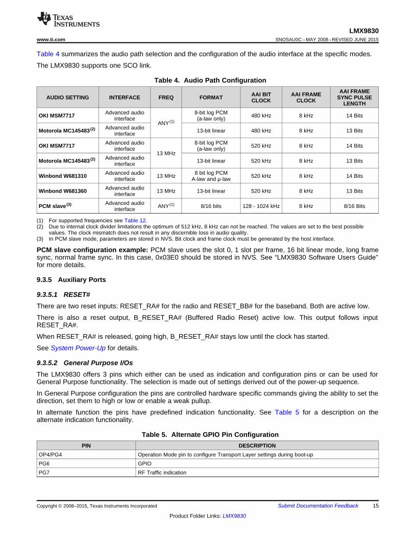
Table 4 summarizes the audio path selection and the configuration of the audio interface at the specific modes.
The LMX9830 supports one SCO link.
Table 4. Audio Path ConfigurationAAI FRAMEAAI BIT AAI FRAMEAUDIO SETTING INTERFACE FREQ FORMAT SYNC PULSECLOCK CLOCK LENGTH
Advanced audio 8-bit log PCMOKI MSM7717 480 kHz 8 kHz 14 Bitsinterface (a-law only)ANY (1)
Advanced audioMotorola MC145483 (2) 13-bit linear 480 kHz 8 kHz 13 BitsinterfaceAdvanced audio 8-bit log PCMOKI MSM7717 520 kHz 8 kHz 14 Bitsinterface (a-law only)
13 MHzAdvanced audioMotorola MC145483 (2) 13-bit linear 520 kHz 8 kHz 13 BitsinterfaceAdvanced audio 8 bit log PCMWinbond W681310 13 MHz 520 kHz 8 kHz 14 Bitsinterface A-law and μ-lawAdvanced audioWinbond W681360 13 MHz 13-bit linear 520 kHz 8 kHz 13 BitsinterfaceAdvanced audioPCM slave (3) ANY (1) 8/16 bits 128 - 1024 kHz 8 kHz 8/16 Bitsinterface
(1) For supported frequencies see Table 12.(2) Due to internal clock divider limitations the optimum of 512 kHz, 8 kHz can not be reached. The values are set to the best possible
values. The clock mismatch does not result in any discernible loss in audio quality.(3) In PCM slave mode, parameters are stored in NVS. Bit clock and frame clock must be generated by the host interface.
PCM slave configuration example: PCM slave uses the slot 0, 1 slot per frame, 16 bit linear mode, long framesync, normal frame sync. In this case, 0x03E0 should be stored in NVS. See “LMX9830 Software Users Guide”for more details.
9.3.5 Auxiliary Ports
9.3.5.1 RESET#There are two reset inputs: RESET_RA# for the radio and RESET_BB# for the baseband. Both are active low.
There is also a reset output, B_RESET_RA# (Buffered Radio Reset) active low. This output follows inputRESET_RA#.
When RESET_RA# is released, going high, B_RESET_RA# stays low until the clock has started.
See System Power-Up for details.
9.3.5.2 General Purpose I/OsThe LMX9830 offers 3 pins which either can be used as indication and configuration pins or can be used forGeneral Purpose functionality. The selection is made out of settings derived out of the power-up sequence.
In General Purpose configuration the pins are controlled hardware specific commands giving the ability to set thedirection, set them to high or low or enable a weak pullup.
In alternate function the pins have predefined indication functionality. See Table 5 for a description on thealternate indication functionality.
Table 5. Alternate GPIO Pin ConfigurationPIN DESCRIPTION
OP4/PG4 Operation Mode pin to configure Transport Layer settings during boot-upPG6 GPIOPG7 RF Traffic indication
Copyright © 2008–2015, Texas Instruments Incorporated Submit Documentation Feedback 15
Product Folder Links: LMX9830

LMX9830SNOSAU0C –MAY 2008–REVISED JUNE 2015 www.ti.com
9.3.6 System Power UpIn order to correctly power up the LMX9830, the following sequence is recommended to be performed:
Apply VCC_IO and VCC to the LMX9830.
The RESET_RA# should be driven high. Then RESET_BB# should be driven high at a recommended time of 1ms after the LMX9830 voltage rails are high. The LMX9830 is properly reset.
See Figure 8.
ESR of the crystal also has impact on the start-up time of the crystal oscillator circuit of the LMX9830 (SeeTable 6 and Table 7).
Figure 8. LMX9830 Power-On Reset Timing
Table 6. LMX9830 Power to Reset TimingSYMBOL PARAMETER CONDITION MIN TYP MAX UNIT
tPTORRA VCC and VCC_IO at operating voltagePower to Reset _RA# <500 (1) µslevel to valid resettPTORBB VCC and VCC_IO at operating voltageReset_RA# to Reset_BB# 1 (2) mslevel to valid reset
(1) Rise time on power must switch on fast, rise time <500 µs.(2) Recommended value.
Table 7. ESR vs Start-up TimeESR (Ω) TYPICAL (1) (2) UNIT
10 12 ms25 13 ms40 16 ms50 24 ms80 30 ms
(1) Frequency, loading caps and ESR all must be considered for determining start-up time.(2) For reference only, must be tested on each system to accurately design POR and correctly start up system.
16 Submit Documentation Feedback Copyright © 2008–2015, Texas Instruments Incorporated
Product Folder Links: LMX9830
LMX9830www.ti.com SNOSAU0C –MAY 2008–REVISED JUNE 2015
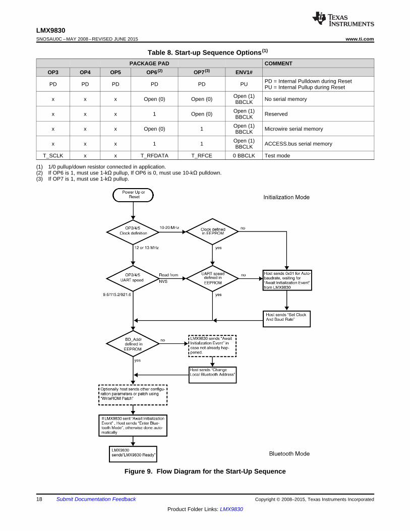
9.3.7 Start-up SequenceDuring start-up, the LMX9830 checks the options register pins OP3 to OP7 for configuration on operation mode,external clock source, transport layer and available nonvolatile storage PROM.
The different options for start-up are described in Table 8.
9.3.7.1 Options RegisterExternal pads in Table 8 are latched in this register at the end of Reset. The Options register can be read byfirmware at any time.
All pads are inputs with weak on-chip pullup/down resistors during Reset. Resistors are disconnected at the endof RESET_BB#.
1 = Pullup resistor connected in application
0 = Pulldown resistor connected in application
x = Don’t care
9.3.7.2 Start-up With External PROM AvailableTo be able to read out information from an external PROM the option pins must be set according to Table 8.
Start-up sequence activities:1. From the Options registers OP6 and OP7, the LMX9830 checks if a serial PROM is available to use
(ACCESS.bus or Microwire).2. If serial PROM is available, the permanent parameter block, patch block, and nonvolatile storage (NVS) are
read from it. If the BD Address is not present, enter the BD address to be saved in the NVS. For moreinformation see Configuring the LMX9830 Through Transport Layer.
3. From the Options register OP3, OP4 and OP5, the LMX9830 checks for clocking information and transportlayer settings. If the NVS information are not sufficient, the LMX9830 will send the “Await Initialization” eventon the TL (Transport Layer) and wait for additional information (see Start-up Without External PROMAvailable.)
4. The LMX9830 compensates the UART for new BBCLK information from the NVS.5. The LMX9830 starts up the Bluetooth core.
9.3.7.3 Start-up Without External PROM AvailableThe following sequence will take place if OP6 and OP7 have been set to “No external memory” as described inTable 8.
Start-up sequence activities:1. From the Options registers OP6 and OP7, the LMX9830 checks if a serial PROM is available to use.2. From the Options register OP3, OP4 and OP5, the LMX9830 checks for clocking mode and transport layer.3. The LMX9830 sends the “Await Initialization” Event on the TL (Transport Layer) and waits for NVS
configuration commands. The configuration is finalized by sending the “Enter Bluetooth Mode” command.4. The LMX9830 compensates the UART for new BBCLK information from the NVS.5. The LMX9830 starts up the Bluetooth core.
Copyright © 2008–2015, Texas Instruments Incorporated Submit Documentation Feedback 17
Product Folder Links: LMX9830
LMX9830SNOSAU0C –MAY 2008–REVISED JUNE 2015 www.ti.com
Table 8. Start-up Sequence Options (1)
PACKAGE PAD COMMENTOP3 OP4 OP5 OP6 (2) OP7 (3) ENV1#
PD = Internal Pulldown during ResetPD PD PD PD PD PU PU = Internal Pullup during ResetOpen (1)x x x Open (0) Open (0) No serial memoryBBCLKOpen (1)x x x 1 Open (0) ReservedBBCLKOpen (1)x x x Open (0) 1 Microwire serial memoryBBCLKOpen (1)x x x 1 1 ACCESS.bus serial memoryBBCLK
T_SCLK x x T_RFDATA T_RFCE 0 BBCLK Test mode
(1) 1/0 pullup/down resistor connected in application.(2) If OP6 is 1, must use 1-kΩ pullup, If OP6 is 0, must use 10-kΩ pulldown.(3) If OP7 is 1, must use 1-kΩ pullup.
Figure 9. Flow Diagram for the Start-Up Sequence
18 Submit Documentation Feedback Copyright © 2008–2015, Texas Instruments Incorporated
Product Folder Links: LMX9830

LMX9830www.ti.com SNOSAU0C –MAY 2008–REVISED JUNE 2015
Table 9. Fixed FrequenciesOSC FREQ. BBCLK (MHz) PLL (48 MHz) OP3 (1) OP4 (2) OP5 (3) FUNCTION(MHz)
12 12 OFF 0 0 0 UART speed read from NVSClock and UART baudrate10-20 (4) 10-20 (1) ON 0 1 0 detection
13 13 OFF 1 0 0 UART speed read from NVS13 13 OFF 1 0 1 UART speed 9.6 kbps13 13 OFF 1 1 0 UART speed 115.2 kbps13 13 OFF 1 1 1 UART speed 921.6 kbps
(1) If OP3 is 1, must use 1-kΩ pullup.(2) If OP4 is 1, must use 1-kΩ pullup.(3) If OP5 is 1, must use 1-kΩ pullup.(4) Supported frequencies see Table 13.
9.3.7.4 Configuring the LMX9830 Through Transport LayerAs described in System Power-Up, the LMX9830 will check during start-up the Options Registers if an externalPROM is available. If the information on the PROM are incomplete or no PROM is installed the LMX9830 willboot into the “initialization Mode”.
The mode is confirmed by the “Await Initialization” Event.
The following information are needed to enter Bluetooth Mode:• Bluetooth Device Address (BD_Addr)• External clock source (only if 10 - 20 MHz has been selected)• UART Baudrate (only if Auto baudrate detection has been selected)
In general the following procedure will initialize the LMX9830:1. Wait for “Await initialization” Event
– Event will only appear if transport layer speed is set or after successful baudrate detection.2. Send “Set Clock and Baudrate” Command only if the clock speed is not known through hardware
configuration (i.e only if OP3, OP4, OP5 = 0 1 0).3. Send “Write BD_Addr” to Configure Local Bluetooth Device Address.4. Send “Enter Bluetooth Mode”
– LMX9830 will use configured clock and UART speed and start the command interface.
Note: In case no EEPROM is used, BDAddr, clock source and Baudrate are only valid until the next power-cycleor hardware reset.
9.3.7.5 Auto Baud Rate DetectionThe LMX9830 supports an Automatic Baudrate Detection in case the external clock is different to 12, 13 MHz orthe range 10-20 MHz or the baudrate is different to 9.6 kbps, 115.2 or 921.6 kbit/s.
The baudrate detection is based on the measurement of one character. The following issues need to beconsidered:• The flow control pin CTS must be low or else the host is in flow stop.• The Auto Baudrate Detector measures the length of the 0x01 character from the positive edge of bit 0 to the
positive edge of stop bit.• Therefore the very first received character must always be a 0x01.• The host can restrict itself to send only a 0x01 character or also can send a command.• The host must flush the TX buffer within 50-100 milliseconds depend on clock frequency on the host
controller.• After 50-100 milliseconds the UART is about to be initialized and short after the host should receive a “Await
Initialization” Event or an “Command Status” Event.
Copyright © 2008–2015, Texas Instruments Incorporated Submit Documentation Feedback 19
Product Folder Links: LMX9830

LMX9830SNOSAU0C –MAY 2008–REVISED JUNE 2015 www.ti.com
Figure 10. Auto Baudrate Detection Timing Diagram
9.3.8 Using an External EEPROM for Nonvolatile DataThe LMX9830 offers two interfaces to connect to external memory. Depending on the EEPROM used, theinterface is activated by setting the correct option pins during start-up. See Table 8 for the option pin settings.
The external memory is used to store mandatory parameters like the BD_Address as well as many optionalparameters like Link Keys or even User data.
The NVM is organized with fixed addresses for the parameters. Because of that the EEPROM can bepreprogrammed with default parameters in manufacturing. Refer to Table 36 for the organization of the NVSmap.
In case the external memory is empty on first start-up, the LMX9830 will behave as like no memory is connected.(See Start-up Without External PROM Available). During the start-up process, parameters can be written directlyto the EEPROM to be available after next bootup. On first bootup, the EEPROM will be automaticallyprogrammed to default values, including the UART speed of 9600 BPS. Patches supplied over the TL will bestored automatically into the EEPROM.
9.3.9 Integrated FirmwareThe LMX9830 includes the full Bluetooth stack up to RFComm to support the following profiles:• GAP (Generic Access Profile)• SDAP (Service Discovery Application Profile)• SPP (Serial Port Profile)
Figure 11 shows the Bluetooth protocol stack with command interpreter interface. The command interpreteroffers a number of different commands to support the functionality given by the different profiles. Execution andinterface timing is handled by the control application.
The chip has an internal data area in RAM that includes the parameters shown in Table 36.
Figure 11. LMX9830 Software Implementation
20 Submit Documentation Feedback Copyright © 2008–2015, Texas Instruments Incorporated
Product Folder Links: LMX9830

LMX9830www.ti.com SNOSAU0C –MAY 2008–REVISED JUNE 2015
9.3.10 Digital Smart Radio
9.3.10.1 Functional DescriptionThe integrated Digital Smart Radio uses a heterodyne receiver architecture with a low intermediate frequency (2MHz) such that the intermediate frequency filters can be integrated on chip. The receiver consists of a low-noiseamplifier (LNA) followed by two mixers. The intermediate frequency signal processing blocks consist of a poly-phase bandpass filter (BPF), two hard-limiters (LIM), a frequency discriminator (DET), and a post-detection filter(PDF). The received signal level is detected by a received signal strength indicator (RSSI).
The received frequency equals the local oscillator frequency (fLO) plus the intermediate frequency (fIF):
fRF = fLO + fIF (supradyne).
The radio includes a synthesizer consisting of a phase detector, a charge pump, an (off-chip) loop-filter, an RF-frequency divider, and a voltage controlled oscillator (VCO).
The transmitter uses IQ-modulation with bit-stream data that is gaussian filtered. Other blocks included in thetransmitter are a VCO buffer and a power amplifier (PA).
9.3.10.2 Receiver Front-EndThe receiver front-end consists of a low-noise amplifier (LNA) followed by two mixers and two low-pass filters forthe I- and Q-channels.
The intermediate frequency (IF) part of the receiver front-end consists of two IF amplifiers that receive inputsignals from the mixers, delivering balanced I- and Q-signals to the poly-phase bandpass filter. The poly-phasebandpass filter is directly followed by two hard-limiters that together generate an AD-converted RSSI signal.
9.3.10.2.1 Poly-Phase Bandpass Filter
The purpose of the IF bandpass filter is to reject noise and spurious (mainly adjacent channel) interference thatwould otherwise enter the hard limiting stage. In addition, it takes care of the image rejection.
The bandpass filter uses both the I- and Q-signals from the mixers. The out-of-band suppression should behigher than 40 dB (f<1 MHz, f>3 MHz). The bandpass filter is tuned over process spread and temperaturevariations by the autotuner circuitry. A 5th order Butterworth filter is used.
9.3.10.2.2 Hard-Limiter and RSSI
The I- and Q-outputs of the bandpass filter are each followed by a hard-limiter. The hard-limiter has its ownreference current. The RSSI (Received Signal Strength Indicator) measures the level of the RF input signal.
The RSSI is generated by piece-wise linear approximation of the level of the RF signal. The RSSI has a mV/dBscale, and an analog-to-digital converter for processing by the baseband circuit. The input RF power is convertedto a 5-bit value. The RSSI value is then proportional to the input power (in dBm).
The digital output from the ADC is sampled on the BPKTCTL signal low-to-high transition.
9.3.10.3 Receiver Back-EndThe hard-limiters are followed by a two frequency discriminators. The I-frequency discriminator uses the 90×phase-shifted signal from the Q-path, while the Q-discriminator uses the 90× phase-shifted signal from the I-path.A poly-phase bandpass filter performs the required phase shifting. The output signals of the I- and Q-discriminator are substracted and filtered by a low-pass filter. An equalizer is added to improve the eye-patternfor 101010 patterns.
After equalization, a dynamic AFC (automatic frequency offset compensation) circuit and slicer extract theRX_DATA from the analog data pattern. It is expected that the Eb/No of the demodulator is approximately 17 dB.
9.3.10.3.1 Frequency Discriminator
The frequency discriminator gets its input signals from the limiter. A defined signal level (independent of thepower supply voltage) is needed to obtain the input signal. Both inputs of the frequency discriminator havelimiting circuits to optimize performance. The bandpass filter in the frequency discriminator is tuned by theautotuning circuitry.
Copyright © 2008–2015, Texas Instruments Incorporated Submit Documentation Feedback 21
Product Folder Links: LMX9830
LMX9830SNOSAU0C –MAY 2008–REVISED JUNE 2015 www.ti.com
9.3.10.3.2 Post-Detection Filter and Equalizer
The output signals of the FM discriminator first go through a post-detection filter and then through an equalizer.Both the post-detection filter and equalizer are tuned to the proper frequency by the autotuning circuitry. Thepost-detection filter is a low-pass filter intended to suppress all remaining spurious signals, such as the secondharmonic (4 MHz) from the FM detector and noise generated after the limiter.
The post-detection filter also helps for attenuating the first adjacent channel signal. The equalizer improves theeye-opening for 101010 patterns. The post-detection filter is a third order Butterworth filter.
9.3.10.4 Autotuning CircuitryThe autotuning circuitry is used for tuning the bandpass filter, the detector, the post-detection filter, the equalizer,and the transmit filters for process and temperature variations. The circuit also includes an offset compensationfor the FM detector.
9.3.10.5 SynthesizerThe synthesizer consists of a phase-frequency detector, a charge pump, a low-pass loop filter, a programmablefrequency divider, a voltage-controlled oscillator (VCO), a delta-sigma modulator, and a lookup table.
The frequency divider consists of a divide-by-2 circuit (divides the 5 GHz signal from the VCO down to 2.5 GHz),a divide-by-8-or-9 divider, and a digital modulus control. The delta-sigma modulator controls the division ratio andalso generates an input channel value to the lookup table.
9.3.10.5.1 Phase-Frequency Detector
The phase-frequency detector is a 5-state phase-detector. It responds only to transitions, hence phase-error isindependent of input waveform duty cycle or amplitude variations. Loop lockup occurs when all the negativetransitions on the inputs, F_REF and F_MOD, coincide. Both outputs (that is, Up and Down) then remain high.This is equal to the zero error mode. The phase-frequency detector input frequency range operates at 12 MHz.
9.3.10.6 Transmitter CircuitryThe transmitter consists of ROM tables, two Digital to Analog (DA) converters, two low-pass filters, IQ mixers,and a power amplifier (PA).
The ROM tables generate a digital IQ signal based on the transmit data. The output of the ROM tables isinserted into IQ-DA converters and filtered through two low-pass filters. The two signal components are mixed upto 2.5 GHz by the TX mixers and added together before being inserted into the transmit PA.
9.3.10.6.1 IQ-DA Converters and TX Mixers
The ROM output signals drive an I- and a Q-DA converter. Two Butterworth low-pass filters filter the DA outputsignals. The 6-MHz clock for the DA converters and the logic circuitry around the ROM tables are derived fromthe autotuner.
The TX mixers mix the balanced I- and Q-signals up to 2.4-2.5 GHz. The output signals of the I- and Q-mixersare summed.
9.3.10.7 Crystal RequirementsThe LMX9830 contains a crystal driver circuit. This circuit operates with an external crystal and capacitors toform an oscillator. shows the recommended crystal circuit. Table 13 specifies system clock requirements.
The RF local oscillator and internal digital clocks for the LMX9830 is derived from the reference clock at theCLK+ input. This reference may either come from an external clock or a dedicated crystal oscillator. The crystaloscillator connections require an Xtal and two grounded capacitors.
It is also important to consider board and design dependant capacitance in tuning crystal circuit. Equations thatfollow allow a close approximation of crystal tuning capacitance required, but actual values on board will varywith capacitive properties of the board. As a result, some fine tuning of crystal circuit that must be done thatcannot be calculated; tuning must be done by testing different values of load capacitance.
22 Submit Documentation Feedback Copyright © 2008–2015, Texas Instruments Incorporated
Product Folder Links: LMX9830
LMX9830www.ti.com SNOSAU0C –MAY 2008–REVISED JUNE 2015
Many different crystals can be used with the LMX9830. Key requirements from Bluetooth specification is + 20ppm. Additionally, ESR (Equivalent Series Resistance) must be carefully considered. LMX9830 can supportmaximum of 230 Ω ESR, but it is recommended to stay <100 Ω ESR for best performance over voltage andtemperature. Reference Figure 17 for ESR as part of crystal circuit for more information.
9.3.10.7.1 Crystal
The crystal appears inductive near its resonant frequency. It forms a resonant circuit with its load capacitors. Theresonant frequency may be trimmed with the crystal load capacitance.1. Load Capacitance: For resonance at the correct frequency, the crystal should be loaded with its specified
load capacitance, which is the value of capacitance used in conjunction with the crystal unit. Loadcapacitance is a parameter specified by the crystal, typically expressed in pF. The crystal circuit shown inFigure 13 is composed of:– C1 (motional capacitance)– R1 (motional resistance)– L1 (motional inductance)– C0 (static or shunt capacitance)The LMX9830 provides some of the load with internal capacitors Cint. The remainder must come from theexternal capacitors and tuning capacitors labeled Ct1 and Ct2 as shown in Figure 12. Ct1 and Ct2 shouldhave the same the value for best noise performance. The LMX9830 has an additional internal capacitanceCTUNE of 2.6 pF. Crystal load capacitance (CL) is calculated as the following:
CL = Cint + CTUNE + Ct1//Ct2 (1)
The CL above does not include the crystal internal self-capacitance C0 as shown in Figure 13, so the totalcapacitance is:
Ctotal = CL + C0 (2)
Based on crystal spec and equation:CL = Cint + CTUNE + Ct1//Ct2 (3)CL = 8 pF + 2.6 pF + 6 pF = 16.6 pF (4)
16.6 pF is very close to the TEW crystal requirement of 16 pF load capacitance. With the internal shuntcapacitance Ctotal:
Ctotal = 16.6 pF + 5 pF = 21.6 pF (5)2. Crystal Pullability: Pullability is another important parameter for a crystal, which is the change in frequency of
a crystal with units of ppm/pF, either from the natural resonant frequency to a load resonant frequency, orfrom one load resonant frequency to another. The frequency can be pulled in a parallel resonant circuit bychanging the value of load capacitance. A decrease in load capacitance causes an increase in frequency,and an increase in load capacitance causes a decrease in frequency.
3. Frequency Tuning: Frequency Tuning is achieved by adjusting the crystal load capacitance with externalcapacitors. It is a Bluetooth requirement that the frequency is always within ±20 ppm. Crystal/oscillator musthave cumulative accuracy specifications of ±15 ppm to provide margin for frequency drift with aging andtemperature.
TEW Crystal: The LMX9830 has been tested with the TEW TAS-4025A crystal, reference Table 10 forspecification. Because the internal capacitance of the crystal circuit is 8 pF and the load capacitance is 16pF, 12 pF is a good starting point for both Ct1 and Ct2. The 2480-MHz RF frequency offset is then tested.Figure 14 shows the RF frequency offset test results.
Figure 14 shows the results are –20 kHz off the center frequency, which is –1 ppm. The pullability of thecrystal is 2 ppm/pF, so the load capacitance must be decreased by about 1.0 pF. By changing Ct1 or Ct2 to10 pF, the total load capacitance is decreased by 1.0 pF. Figure 15 shows the frequency offset test results.The frequency offset is now zero with Ct1 = 10 pF, Ct2 = 10 pF.
Reference Table 11 for crystal tuning values used on Mesa Development Board with TEW crystal.
Copyright © 2008–2015, Texas Instruments Incorporated Submit Documentation Feedback 23
Product Folder Links: LMX9830

LMX9830SNOSAU0C –MAY 2008–REVISED JUNE 2015 www.ti.com
Figure 12. LMX9830 Crystal Recommended Circuit
Figure 13. Crystal Equivalent Circuit
Table 10. TEW TAS-4025ASPECIFICATION VALUE
Package 4.0 × 2.5 × 0.65 mm - 4 padsFrequency 13.000 MHzMode FundamentalStability > ±15 ppm @ –40 to +85°CCL Load Capacitance 16 pFESR 80 Ω max.C0 Shunt Capacitance 5 pFDrive Level 50 ±10 µVPullability 2 ppm/pF minStorage Temperature –40 to 85°C
Table 11. TEW on LMX9830 DONGLEREFERENCE LMX9830
Ct1 12 pFCt2 12 pF
24 Submit Documentation Feedback Copyright © 2008–2015, Texas Instruments Incorporated
Product Folder Links: LMX9830

LMX9830www.ti.com SNOSAU0C –MAY 2008–REVISED JUNE 2015
Figure 14. Frequency Offset with 12 pF//12 pF Capacitors Figure 15. Frequency Offset with 10 pF//10 pF Capacitors
9.3.10.7.2 TCXO (Temperature Compensated Crystal Oscillator)
The LMX9830 also can operate with an external TCXO (Temperature Compensated Crystal Oscillator). TheTCXO signal is directly connected to the CLK+.• Input Impedance: The LMX9830 CLK+ pin has in input impedance of 2 pF capacitance in parallel with >400
kW resistance.
9.3.10.7.3 Optional 32-kHz Oscillator
A second oscillator is provided (see Figure 16) that is tuned to provide optimum performance and low-powerconsumption while operating with a 32.768-kHz crystal. An external crystal clock network is required between theX2_CKI clock input and the X2_CKO clock output signals. The oscillator is built in a Pierce configuration anduses two external capacitors. Table 12 provides the oscillator’s specifications.
In case the 32 kHz is not used, it is recommended to leave X2_CKO open and connect X2_CKI to GND.
Figure 16. 32.768-kHz Oscillator
Table 12. 32.768-kHz Oscillator SpecificationsPARAMETER TEST CONDITIONS MIN TYP MAX UNIT
VDD Supply Voltage 1.62 1.8 1.98 VIDDACT Supply Current (Active) 2 µAf Nominal Output Frequency 32.768 kHzVPPOSC Oscillating Amplitude 1.8 V
Duty Cycle 40% 60% —
Copyright © 2008–2015, Texas Instruments Incorporated Submit Documentation Feedback 25
Product Folder Links: LMX9830
LMX9830SNOSAU0C –MAY 2008–REVISED JUNE 2015 www.ti.com
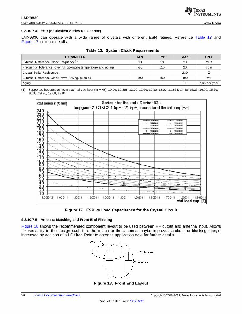
9.3.10.7.4 ESR (Equivalent Series Resistance)
LMX9830 can operate with a wide range of crystals with different ESR ratings. Reference Table 13 andFigure 17 for more details.
Table 13. System Clock RequirementsPARAMETER MIN TYP MAX UNIT
External Reference Clock Frequency (1) 10 13 20 MHzFrequency Tolerance (over full operating temperature and aging) -20 ±15 20 ppmCrystal Serial Resistance 230 ΩExternal Reference Clock Power Swing, pk to pk 100 200 400 mVAging ±1 ppm per year
(1) Supported frequencies from external oscillator (in MHz): 10.00, 10.368, 12.00, 12.60, 12.80, 13.00, 13.824, 14.40, 15.36, 16.00, 16.20,16.80, 19.20, 19.68, 19.80
Figure 17. ESR vs Load Capacitance for the Crystal Circuit
9.3.10.7.5 Antenna Matching and Front-End Filtering
Figure 18 shows the recommended component layout to be used between RF output and antenna input. Allowsfor versatility in the design such that the match to the antenna maybe improved and/or the blocking marginincreased by addition of a LC filter. Refer to antenna application note for further details.
Figure 18. Front End Layout
26 Submit Documentation Feedback Copyright © 2008–2015, Texas Instruments Incorporated
Product Folder Links: LMX9830

1 + ZC2 À T22
(1 + ZC2 À T12)(1 + ZC
2 À T32)ZC
2 À N
A0 = À
KIÀ KVCO
A1 = A0 À (T1 + T3)
|
A2 = A0 À T1 À T3
T3 = T31 u T1 T2 =ZC
2 À (T1 + T3)
J
I = tan-1 ZC À T1 À T1 + T31
J
¹·
©§ tan-1(ZC À T1)tan-1(ZC À T1 À T31)
and ZC = 2SFCN =Fout
Fcomp
LMX9830www.ti.com SNOSAU0C –MAY 2008–REVISED JUNE 2015
9.3.10.7.6 Loop Filter Design
The LMX9830 has an external loop filter which must be designed for best performance by the end customer.This section therefore gives some foresight into its design. Refer also to Loop Filter application note and TI'sWebench on-line design tool for more information.
9.3.10.7.6.1 Component Calculations
The following parameters are required for component value calculation of a third order passive loop filter.
Φ Phase Margin: Phase of the open loop transfer function
Fc Loop Bandwidth
Fcomp Comparison Frequency: Phase detector frequency
KVOC VCO gain: Sensitivity of the VCO to control volts
KΦ Charge Pump gain: Magnitude of the alternating current during lock
FOUT Maximum RF output frequency
T31 Ratio of the poles T3 to T1 in a 3rd order filter
γ Gamma optimization parameter
The third order loop filter being defined has the following topology. shown in Figure 19.
Figure 19. Third Order Loop Filter
(6)
Calculate the poles and zeros. Use exact method to solve for T1 using numerical methods,
(7)
(8)
Calculate the loop filter coefficients,
(9)
Copyright © 2008–2015, Texas Instruments Incorporated Submit Documentation Feedback 27
Product Folder Links: LMX9830

R2 =T2C2
R3 =A2
C1 À C3 À T2
C2 = A0 C1 C3C3 =T22 À C1 A2
1 À T22 À C12 + T2 À A1 À C1 A2 À A0
T2 À A0 T2 À A1
A2T22 ¸¹
ᬩ
§C1 = À (1 + 1 +
A2
LMX9830SNOSAU0C –MAY 2008–REVISED JUNE 2015 www.ti.com
Summary:
SYMBOL DESCRIPTION UNITn N counter value None
Loop Bandwidth rad/sT1 Loop filter pole ST2 Loop filter zero ST3 Loop filter zero SA0 Total capacitance nFA1 First order loop filter coefficient nFsA2 Second order loop filter coefficient nFs2
Components can then be calculated from loop filter coefficients
(10)
(11)
(12)
Some typical values for the LMX9830 are:
Table 14. Typical ValuesDESCRIPTION VALUE UNITComparison Frequency 13 MHzPhase Margin 48 Pl radLoop bandwidth 100 kHzT3 over T1 ratio 40%Gamma 1.0VCO gain 120 MHz per VCharge pump gain 0.6 mAFout 2441 MHz
Which give the following component values:
Table 15. Component ValuesDESCRIPTION VALUE UNITC1 0.17 nFC2 2.38 nFC3 0.04 nFR2 1737 ΩR3 7025 Ω
9.3.10.7.6.2 Phase Noise and Lock-Time Calculations
Phase noise has three sources, the VCO, crystal oscillator and the rest of the PLL consisting of the phasedetector, dividers, charge pump and loop filter. Assuming the VCO and crystal are very low noise, it is possible toput down approximate equations that govern the phase noise of the PLL.
Phase noise (in-band) = PN1Hz + 20Log[N] + 10Log[Fcomp]
where
28 Submit Documentation Feedback Copyright © 2008–2015, Texas Instruments Incorporated
Product Folder Links: LMX9830

LT =400FC
Where 'F =Frequency tolerance
(1 log10'F)Frequency jump
LMX9830www.ti.com SNOSAU0C –MAY 2008–REVISED JUNE 2015
• PH1Hz is the PLL normalized noise floor in 1 Hz resolution bandwidth (13)
Further out from the carrier, the phase noise will be affected by the loop filter roll-off and hence its bandwidth.
As a rule-of-thumb;ΔPhase noise = 40Log[ΔFc]
where• Fc is the relative change in loop BW expressed as a fraction (14)
For example if the loop bandwidth is reduced from 100 kHz to 50 kHz or by one half, then the change in phasenoise will be -12dB. Loop BW in reality should be selected to meet the lower limit of the modulation deviation,this will yield the best possible phase noise.
Even further out from the carrier, the phase noise will be mainly dominated by the VCO noise assuming thecrystal is relatively clean.
Lock-time is dependent on three factors, the loop bandwidth, the maximum frequency jump that the PLL mustmake and the final tolerance to which the frequency must settle. As a rule-of-thumb it is given by:
(15)
These equations are approximations of the ones used by Webench to calculate phase noise and lock-time.
9.3.10.7.6.3 Practical Optimization
In an example where frequency drift and drift rate can be improved though loop filter tweaks, consider the resultstaken below. The drift rate is 26.1 kHz per 50 μs and the maximum drift is 25 kHz for DH1 packets, both of whichare exceeding or touching the Bluetooth pass limits. These measurements are taken with component valuesshown in Table 15.
Table 16. Loop Filter Optimization Example – Before OptimizationTRM/CA/09/C (CARRIER DRIFTHOPPONG ON- LOW CHANNEL
DH1 DH3 DH5 LIMITSDrift Rate/50 μs 26.1 kHz N/A −30.5 kHz ±20 kHzMax Drift 25 kHz N/A 36 kHz DHI: ±25 kHzAverage Drift −1 kHz N/A 12 kHz DH3: ±40 kHzPackets Tested 10 N/A 10 D5I: ±40 kHzPackets Failed 2 N/A 10Overall Result Failed N/A Failed
Results in Table 17 were taken on the same board with three loop filter values changed. C2 and R2 have beenincreased in value and C1 has been reduced. The drift rate has improved by 13 kHz per 50 µs and the maximumdrift has improved by 10 kHz.
Table 17. Loop Filter Optimization Example – After OptimizationTRM/CA/09/C (CARRIER DRIFTHOPPONG ON- LOW CHANNEL
DH1 DH3 DH5 LIMITSDrift Rate/50 μs −13.6 kHz N/A −15.6 kHz ±20 kHzMax Drift 15 kHz N/A 21 kHz DHI: ±25 kHzAverage Drift 3 kHz N/A 1 kHz DH3: ±40 kHzPackets Tested 10 N/A 10 D5I: ±40 kHzPackets Failed 0 N/A 0Overall Result Passed N/A Passed
Copyright © 2008–2015, Texas Instruments Incorporated Submit Documentation Feedback 29
Product Folder Links: LMX9830

LMX9830SNOSAU0C –MAY 2008–REVISED JUNE 2015 www.ti.com
The effect of changing these three components is to reduce the loop bandwidth which reduces the phase noise.The reduction in this noise level corresponds directly to the reduction of noise in the payload area where drift ismeasured. This noise reduction comes at the expense of lock-time which can be increased to 120 µs withoutsuffering any ill effects, however if we continue to reduce the loop BW further the lock-time will increase such thatthe PLL does not have time to lock before data transmission and the drift will again increase. Before the lock-time goes out of spec, the modulation index will start to fall because it is being cut by the reducing loop BW.Therefore, a compromise must be found between lock-time, phase noise and modulation, which yields bestperformance.
Note: The values shown in the LMX9830 data sheet, are the best case optimized values that have been shownto produce the best overall results and are recommended as a starting point for this design.
Another example of how the loop filter values can affect frequency drift rate, these results below show the DUTwith maximum drift on mid and high channels failing. Adjusting the loop bandwidth as shown provides theimprovement required to pass qualification.
Table 18. Original ResultsHOPPONG ON- LOW CHANNEL
DH1 DH3 DH5 LIMITSDrift Rate/50 μs15.00 15.00 kHz −28.10 kHz −19.10 kHz ±20 kHzMaximum Drift 19 kHz −37 kHz −20 kHz DHI: ±25 kHzAverage Drift 11 kHz −32 kHz −10 kHz DH3: ±40 kHzPackets Tested 10 10 10 D5I: ±40 kHzPackets Failed 0 1 0Result Pass Fail PassHOPPONG ON- MED CHANNEL
DH1 DH3 DH5 LIMITSDrift Rate/50 μs 15.00 kHz −28.10 kHz −19.10 kHz ±20 kHzMax Drift 19 kHz −37 kHz −20kHz DHI: ±25 kHzAverage Drift 11 kHz −32 kHz −10 kHz DH3: ±40 kHzPackets Tested 10 10 10 D5I: ±40 kHzPackets Failed 0 1 0Overall Result Pass Fail PassHOPPONG ON- HIGH CHANNEL
DH1 DH3 DH5 LIMITSDrift Rate/50 μs 15.00 kHz −28.10 kHz −19.10 kHz ±20 kHzMax Drift 19 kHz −37 kHz −20kHz DHI: ±25 kHzAverage Drift 11 kHz −32 kHz −10 kHz DH3: ±40 kHzPackets Tested 10 10 10 D5I: ±40 kHzPackets Failed 0 1 0Overall Result Pass Fail Pass
30 Submit Documentation Feedback Copyright © 2008–2015, Texas Instruments Incorporated
Product Folder Links: LMX9830

LMX9830www.ti.com SNOSAU0C –MAY 2008–REVISED JUNE 2015
Table 19. New ResultsHOPPONG ON- LOW CHANNEL
DH1 DH3 DH5 LIMITSDrift Rate/50 μs −12.00 kHz −15.10 kHz 18.8 kHz ±20 kHzMax Drift −15 kHz −35 kHz −19 kHz DHI: ±25 kHzAverage Drift −6 kHz −25 kHz −9 kHz DH3: ±40 kHzPackets Tested 10 10 10 D5I: ±40 kHzPackets Failed 0 0 0Overall Result Pass Pass PassHOPPONG ON- MED CHANNEL
DH1 DH3 DH5 LIMITSDrift Rate/50 μs −14.20 kHz −16.10kHz 17.20 kHz ±20 kHzMax Drift −16 kHz −354 kHz −22 kHz DHI: ±25 kHzAverage Drift −11kHz −27 kHz −9 kHz DH3: ±40 kHzPackets Tested 10 10 10 D5I: ±40 kHzPackets Failed 0 0 0Overall Result Pass Pass PassHOPPONG ON- HIGH CHANNEL
DH1 DH3 DH5 LIMITSDrift Rate/50 μs −12.70 kHz −17.40 kHz 16.50 kHz ±20 kHzMax Drift −23 kHz −29 kHz −25 kHz DHI: ±25 kHzAverage Drift −12 kHz −25 kHz −16 kHz DH3: ±40 kHzPackets Tested 10 10 10 D5I: ±40 kHzPackets Failed 0 0 0Overall Result Pass Pass Pass
9.3.10.7.6.4 Component Values for NSC Reference Designs
Table 20 shows a list of components for the loop filter values used on TI's reference design, (Serial Dongle) theyhave been tweaked and optimized in each case to yield optimum performance for each case. The values differslightly from one platform to another due to board paracitics caused by layout differences.
Table 20. Components for Loop Filter ValuesPLATFORM C8 C7 C9 R23 R14
LMX9830 Dongle 220 pF 2200 pF 39 pF 3.3 k 10 k
9.3.11 Command Interface
The LMX9830 offers Bluetooth functionality in either a self contained slave functionality or over a simplecommand interface. The interface is listening on the UART interface.
The following sections describe the protocol transported on the UART interface between the LMX9830 and thehost in command mode (see Figure 20). In Transparent mode, no data framing is necessary and the device doesnot listen for commands.
9.3.11.1 FramingThe connection is considered “Error free”. But for packet recognition and synchronization, some framing is used.
All packets sent in both directions are constructed per the model shown in Table 21.
9.3.11.1.1 Start and End Delimiter
The “STX” char is used as start delimiter: STX = 0x02. ETX = 0x03 is used as end delimiter.
Copyright © 2008–2015, Texas Instruments Incorporated Submit Documentation Feedback 31
Product Folder Links: LMX9830

LMX9830SNOSAU0C –MAY 2008–REVISED JUNE 2015 www.ti.com
9.3.11.1.2 Packet Type ID
This byte identifies the type of packet. See Table 22 for details.
9.3.11.1.3 Opcode
The opcode identifies the command to execute. The opcode values can be found within the “LMX9830 SoftwareUser’s Guide” included within the LMX9830 Evaluation Board.
9.3.11.1.4 Data Length
Number of bytes in the Packet Data field. The maximum size is defined with 333 data bytes per packet.
9.3.11.1.5 Checksum:
This is a simple Block Check Character (BCC) checksum of the bytes “Packet type”, “Opcode” and “DataLength”. The BCC checksum is calculated as low byte of the sum of all bytes (, if the sum of all bytes is 0x3724,the checksum is 0x24).
Figure 20. Bluetooth Functionality
Table 21. Package FramingSTART PACKET ENDOPCODE DATA LENGTH CHECK SUM PACKET DATADELIMITER TYPE ID DELIMITER1 Byte 1 Byte 1 Byte 2 Bytes 1 Byte <Data Length> Bytes 1 Byte
- - - - - - - - - - - - - Checksum - - - - - - - - - - - - -
Table 22. Packet Type IdentificationID DIRECTION DESCRIPTION
0x52 REQUEST A request sent to the Bluetooth module.'R' (REQ) All requests are answered by exactly one confirm.0x43 Confirm The Bluetooth modules confirm to a request.'C' (CFM) All requests are answered by exactly one confirm.0x69 Indication Information sent from the Bluetooth module that is not a direct confirm to a request.'i' (IND) Indicating status changes, incoming links, or unrequested events.0x72 Response An optional response to an indication.'r' (RES) This is used to respond to some type of indication message.
9.3.11.2 Command Set OverviewThe LMX9830 has a well defined command set to:• Configure the device:
– Hardware settings– Local Bluetooth parameters– Service database
• Set up and handle links
Table 23 through Table 33 show the actual command set and the events coming back from the device. A fulldocumented description of the commands can be found in the “LMX9830 Software User’s Guide”.
Note: For standard Bluetooth operation only commands from Table 23 through Table 25 will be used. Most of theremaining commands are for configuration purposes only.
32 Submit Documentation Feedback Copyright © 2008–2015, Texas Instruments Incorporated
Product Folder Links: LMX9830

LMX9830www.ti.com SNOSAU0C –MAY 2008–REVISED JUNE 2015
Table 23. Device DiscoveryCOMMAND EVENT DESCRIPTION
Inquiry Inquiry Complete Search for devicesDevice Found Lists BDADDR and class of device
Remote Device Name Remote Device Name Confirm Get name of remote device
Table 24. SDAP Client CommandsCOMMAND EVENT DESCRIPTION
SDAP Connect SDAP Connect Confirm Create an SDP connection to remote deviceSDAP Disconnect SDAP Disconnect Confirm Disconnect an active SDAP link
Connection Lost Notification for lost SDAP linkSDAP Service Browse Service Browse Confirm Get the services of the remote deviceSDAP Service Search SDAP Service Search Confirm Search a specific service on a remote deviceSDAP Attribute Request SDAP Attribute Request Confirm Searches for services with specific attributes
Table 25. SPP Link EstablishmentCOMMAND EVENT DESCRIPTIONEstablish SPP Link Establishing SPP Link Confirm Initiates link establishment to a remote device
Link Established Link successfully establishedIncoming Link A remote device established a link to the local device
Set Link Timeout Set Link Timeout Confirm Confirms the Supervision Timeout for the existing LinkGet Link Timeout Get Link Timeout Confirm Get the Supervision Timeout for the existing LinkRelease SPP Link Release SPP Link Confirm Initiate release of SPP linkSPP Send Data SPP Send Data Confirm Send data to specific SPP port
Incoming Data Incoming data from remote deviceTransparent Mode Transparent Mode Confirm Switch to Transparent mode on the UART
Table 26. Storing Default ConnectionsCOMMAND EVENT DESCRIPTION
Connect Default Connection Connect Default Connection Confirm Connects to either one or all stored default connectionsStore Default Connection Store Default Connection Confirm Store device as default connectionGet list of Default Connections List of Default DevicesDelete Default Connections Delete Default Connections Confirm
Table 27. Bluetooth Low Power ModesCOMMAND EVENT DESCRIPTIONSet Default Link Policy Defines the link policy used for any incoming or outgoingSet Default Link Policy Confirm linkGet Default Link Policy Get Default Link Policy Confirm Returns the stored default link policySet Link Policy Set Link Policy Confirm Defines the modes allowed for a specific linkGet Link Policy Get Link Policy Confirm Returns the actual link policy for the linkEnter Sniff Mode Enter Sniff Mode ConfirmExit Sniff Mode Exit Sniff Mode ConfirmEnter Hold Mode Enter Hold Mode Confirm
Power Save Mode Changed Remote device changed power save mode on the link
Copyright © 2008–2015, Texas Instruments Incorporated Submit Documentation Feedback 33
Product Folder Links: LMX9830

LMX9830SNOSAU0C –MAY 2008–REVISED JUNE 2015 www.ti.com
Table 28. Audio Control CommandsCOMMAND EVENT DESCRIPTIONEstablish SCO Link Establish SCO Link Confirm Establish SCO Link on existing RFComm Link
A remote device has established a SCO link to the localSCO Link Established Indicator deviceRelease SCO Link Release SCO Link Confirm Release SCO Link Audio Control
SCO Link Released Indicator SCO Link has been releasedChange SCO Packet Type Change SCO Packet Type Confirm Changes Packet Type for existing SCO link
SCO Packet Type changed indicator SCO Packet Type has been changedSet Audio Settings Set Audio Settings Confirm Set Audio Settings for existing LinkGet Audio Settings Get Audio Settings Confirm Get Audio Settings for existing LinkSet Volume Set Volume Confirm Configure the volumeGet Volume Get Volume Confirm Get current volume settingMute Mute Confirm Mutes the microphone input
Table 29. Wakeup FunctionalityCOMMAND EVENT DESCRIPTIONDisable Transport Layer Disabling the UART Transport Layer and activates theTransport Layer Enabled Hardware Wakeup function
Table 30. SPP Port Configuration and StatusCOMMAND EVENT DESCRIPTIONSet Port Config Set Port Config Confirm Set port setting for the virtual serial port link over the airGet Port Config Get Port Config Confirm Read the actual port settings for a virtual serial port
Notification if port settings were changed from remotePort Config Changed deviceSPP Get Port Status SPP Get Port Status Confirm Returns status of DTR, RTS (for the active RFComm link)SPP Port Set DTR SPP Port Set DTR Confirm Sets the DTR bit on the specified linkSPP Port Set RTS SPP Port Set RTS Confirm Sets the RTS bit on the specified linkSPP Port BREAK SPP Port BREAK Indicates that the host has detected a breakSPP Port Overrun Error SPP Port Overrun Error Confirm Used to indicate that the host has detected an overrun errorSPP Port Parity Error SPP Port Parity Error Confirm Host has detected a parity errorSPP Port Framing Error SPP Port Framing Error Confirm Host has detected a framing error
Indicates that remote device has changed one of the portSPP Port Status Changed status bits
Table 31. Local Bluetooth SettingsCOMMAND EVENT DESCRIPTIONRead Local Name Read Local Name Confirm Read actual friendly name of the deviceWrite Local Name Write Local Name Confirm Set the friendly name of the deviceRead Local BDADDR Read Local BDADDR ConfirmChange Local BDADDR Note: The BDADDR must be obtained from the IEEEChange Local BDADDR Confirm organization. See http://standarts.ieee.org/regauth/oui/Store Class of Device Store Class of Device ConfirmSet Scan Mode Set Scan Mode Confirm Change mode for discoverability and connectability
Set Scan Mode Indication Reports end of Automatic limited discoverable modeGet Fixed Pin Get Fixed Pin Confirm Reads current PinCode stored within the deviceSet Fixed Pin Set Fixed Pin Confirm Set the local PinCode
A PIN code is requested during authentication of an ACLPIN request linkGet Security Mode Get Security Mode Confirm Get actual Security mode
34 Submit Documentation Feedback Copyright © 2008–2015, Texas Instruments Incorporated
Product Folder Links: LMX9830

LMX9830www.ti.com SNOSAU0C –MAY 2008–REVISED JUNE 2015
Table 31. Local Bluetooth Settings (continued)COMMAND EVENT DESCRIPTIONSet Security Mode Set Security Mode Confirm Configure Security mode for local device (default 2)Remove Pairing Remove Pairing Confirm Remove pairing with a remote deviceList Paired Devices Get list of paired devices stored in the LMX9830 dataList of Paired Devices memorySet Default Link Timeout Set Default Link Timeout Confirm Store default link supervision timeoutGet Default Link Timeout Get Default Link Timeout Confirm Get stored default link supervision timeoutForce Master Role Enables/Disables the request for master role at incomingForce Master Role Confirm connections
Table 32. Local Service Database ConfigurationCOMMAND EVENT DESCRIPTIONStore generic SDP Record Store SDP Record Confirm Create a new service record within the service databaseEnable SDP Record Enable SDP Record Confirm Enable or disable SDP recordsDelete All SDP Records Delete All SDP Records ConfirmPorts to Open Ports to Open Confirmed Specify the RFComm Ports to open on start-up
Table 33. Local Hardware CommandsCOMMAND EVENT DESCRIPTIONGet Default Audio Settings Get Default Audio Settings Confirm Get stored Default Audio SettingsSet Default Audio Settings Configure Default Settings for Audio Codec and Air Format,Set Default Audio Settings Confirm stored in NVSSet Event Filter Set Event Filter Confirm Configures the reporting level of the command interfaceGet Event Filter Get Event Filter Confirm Get the status of the reporting levelRead RSSI Read RSSI Confirm Returns an indicator for the incoming signal strengthChange UART Speed Change UART Speed Confirm Set specific UART speed; needs proper ISEL pin settingChange UART Settings Change UART Settings Confirm Change configuration for parity and stop bitsTest Mode Test Mode Confirm Enable Bluetooth, EMI test, or local loopbackRestore Factory Settings Restore Factory Settings ConfirmReset Dongle Ready Soft resetFirmware Upgrade Stops the Bluetooth firmware and executes the In-system-
programming codeSet Clock Frequency Set Clock Frequency Confirm Write Clock Frequency setting in the NVSGet Clock Frequency Get Clock Frequency Confirm Read Clock Frequency setting from the NVSSet PCM Slave Configuration Set PCM Slave Configuration Confirm Write the PCM Slave Configuration in the NVSWrite ROM Patch Write ROM Patch Confirm Store ROM Patch in the SimplyBlue moduleRead Memory Read Memory Confirm Read from the internal RAMWrite Memory Write Memory Confirm Write to the internal RAMRead NVS Read NVS Confirm Read from the NVS (EEPROM)Write NVS Write NVS Confirm Write to the NVS (EEPROM)
Table 34. Initialization CommandsCOMMAND EVENT DESCRIPTIONSet Clock and Baudrate Set Clock and Baudrate Confirm Write Baseband frequency and Baudrate usedEnter Bluetooth Mode Enter Bluetooth Mode Confirm Request SimplyBlue module to enter BT modeSet Clock and Baudrate Set Clock and Baudrate Confirm Write Baseband frequency and Baudrate used
Copyright © 2008–2015, Texas Instruments Incorporated Submit Documentation Feedback 35
Product Folder Links: LMX9830

LMX9830SNOSAU0C –MAY 2008–REVISED JUNE 2015 www.ti.com
Table 35. GPIO Control CommandsCOMMAND EVENT DESCRIPTIONSet GPIO WPU Set GPIO WPU Confirm Enable/Disable weak pullup resistor on GPIOsGet GPIO Input State Get GPIO Input States Confirm Read the status of the GPIOsSet GPIO Direction Set GPIO Direction Confirm Set the GPIOs direction (Input, Ouput)Set GPIO Output High Set GPIO Output High Confirm Set GPIOs Output to logical HighSet GPIO Output Low Set GPIO Output Low Confirm Set GPIOs Output to logical Low
9.4 Device Functional Modes
9.4.1 Operation ModesOn boot-up, the application configures the module following the parameters in the data area.
9.4.1.1 Automatic Operation
9.4.1.1.1 No Default Connections Stored
In Automatic Operation the module is connectable and discoverable and automatically answers to servicerequests. The command interpreter listens to commands and links can be set up. The full command list issupported.
If connected by another device, the module sends an event back to the host, where the RFComm port has beenconnected, and switches to transparent mode.
9.4.1.1.2 Default Connections Stored
If default connections were stored on a previous session, once the LMX9830 is reset, it will attempt to connecteach device stored within the data RAM three times. The host will be notified about the success of the link setupvia a link status event.
9.4.1.1.3 Nonautomatic Operation
In Nonautomatic Operation, the LMX9830 does not check the default connections section within the Data RAM. Ifconnected by another device, it will NOT switch to transparent mode and continue to interpret data sent on theUART.
9.4.1.1.4 Transparent Mode
The LMX9830 supports transparent data communication from the UART interface to a Bluetooth link.
If activated, the module does not interpret the commands on the UART which normally are used to configure andcontrol the module. The packages don’t need to be formatted as described in Table 21. Instead all data aredirectly passed through the firmware to the active Bluetooth link and the remote device.
Transparent mode can only be supported on a point-to-point connection. To leave Transparent mode, the hostmust send a UART_BREAK signal to the module.
9.4.1.1.5 Force Master Mode
In Force Master mode tries to act like an Accesspoint for multiple connections. For this it will only accept the linkif a Master/slave role switch is accepted by the connecting device. After successful link establishment theLMX9830 will be Master and available for additional incoming links. On the first incoming link the LMX9830 willswitch to transparent depending on the setting for automatic or command mode. Additional links will only bepossible if the device is not in transparent mode.
9.4.2 Default ConnectionsThe LMX9830 supports the storage of up to 3 devices within its NVS. Those connections can either beconnected after reset or on demand using a specific command.
36 Submit Documentation Feedback Copyright © 2008–2015, Texas Instruments Incorporated
Product Folder Links: LMX9830

LMX9830www.ti.com SNOSAU0C –MAY 2008–REVISED JUNE 2015
Device Functional Modes (continued)9.4.3 Event FilterThe LMX9830 uses events or indicators to notify the host about successful commands or changes at theBluetooth interface. Depending on the application the LMX9830 can be configured. The following levels aredefined:• No Events:
– The LMX9830 is not reporting any events. Optimized for passive cable replacement solutions.• Standard LMX9830 events:
– Only necessary events will be reported• All events:
– Additional to the standard all changes at the physical layer will be reported.
9.4.4 Default Link PolicyEach Bluetooth Link can be configured to support M/S role switch, Hold Mode, Sniff Mode and Park Mode. Thedefault link policy defines the standard setting for incoming and outgoing connections.
9.4.5 Audio SupportThe LMX9830 offers commands to establish and release synchronous connections (SCO) to support Headset orHandsfree applications. The firmware supports one active link with all available package types (HV1, HV2, HV3),routing the audio data between the Bluetooth link and the advanced audio interface. In order to provide theanalog data interface, an external audio codec is required. The LMX9830 includes a list of codecs which can beused.
Table 36. Operation Parameters Stored in LMX9830PARAMETER DEFAULT VALUE DESCRIPTION
BDADDR (To be requested from IEEE) Bluetooth device addressLocal Name Serial port device Friendly NamePinCode 0000 Bluetooth PinCodeOperation Mode Automatic ON Automatic mode ON or OFFDefault Connections 0 Up to seven default devices to connect toSDP Database 1 SPP entry:
Name: COM1 Service discovery database, control for supported profilesAuthentication and encryption enabled
UART Speed 9600 Sets the speed of the physical UART interface to the hostUART Settings 1 Stop bit, parity disabled Parity and stop bits on the hardware UART interfacePorts to Open 0000 0001 Defines the RFComm ports to openLink Keys No link keys Link keys for paired devicesSecurity Mode 2 Security modePage Scan Mode Connectable Connectable/Not connectable for other devicesInquiry Scan Mode Discoverable/Not Discoverable/Limited Discoverable for otherDiscoverable devicesDefault Link Policy Configures modes allowed for incoming or outgoing connectionsAll modes allowed (Role switch, Hold mode, Sniff mode...)Default Link Timeout The Default Link Timeout configures the timeout, after which the link
20 seconds is assumed lost, if no packages have been received from the remotedevice.
Event Filter Defines the level of reporting on the UART― no eventsStandard LMX9830 events reported ― standard events― standard including ACL link events
Copyright © 2008–2015, Texas Instruments Incorporated Submit Documentation Feedback 37
Product Folder Links: LMX9830
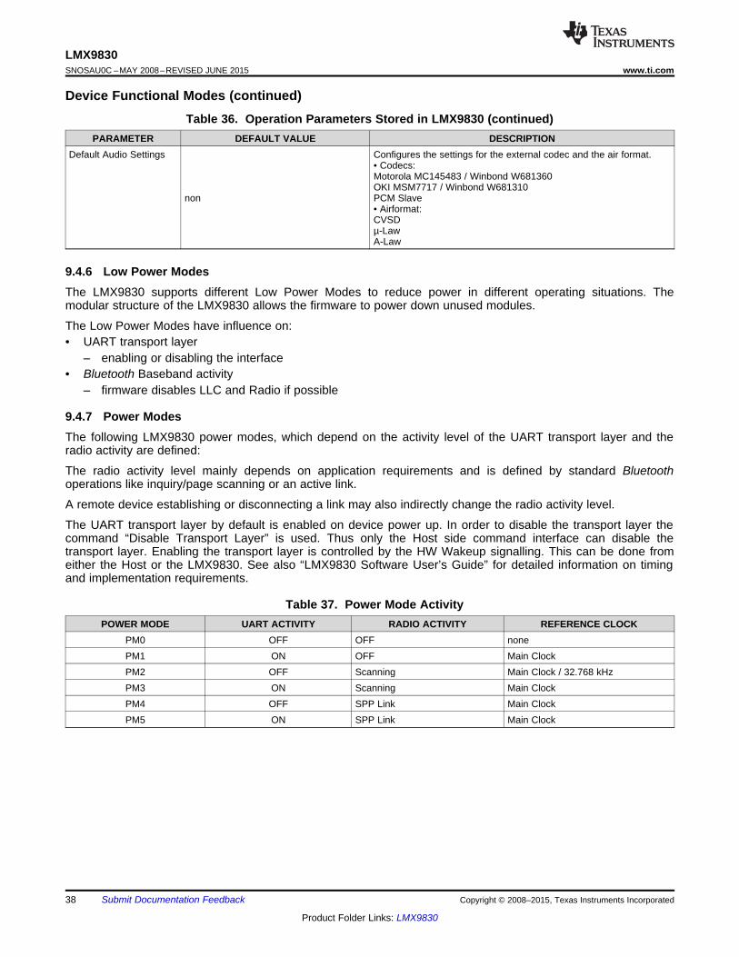
LMX9830SNOSAU0C –MAY 2008–REVISED JUNE 2015 www.ti.com
Device Functional Modes (continued)Table 36. Operation Parameters Stored in LMX9830 (continued)
PARAMETER DEFAULT VALUE DESCRIPTIONDefault Audio Settings Configures the settings for the external codec and the air format.
• Codecs:Motorola MC145483 / Winbond W681360OKI MSM7717 / Winbond W681310
non PCM Slave• Airformat:CVSDµ-LawA-Law
9.4.6 Low Power ModesThe LMX9830 supports different Low Power Modes to reduce power in different operating situations. Themodular structure of the LMX9830 allows the firmware to power down unused modules.
The Low Power Modes have influence on:• UART transport layer
– enabling or disabling the interface• Bluetooth Baseband activity
– firmware disables LLC and Radio if possible
9.4.7 Power ModesThe following LMX9830 power modes, which depend on the activity level of the UART transport layer and theradio activity are defined:
The radio activity level mainly depends on application requirements and is defined by standard Bluetoothoperations like inquiry/page scanning or an active link.
A remote device establishing or disconnecting a link may also indirectly change the radio activity level.
The UART transport layer by default is enabled on device power up. In order to disable the transport layer thecommand “Disable Transport Layer” is used. Thus only the Host side command interface can disable thetransport layer. Enabling the transport layer is controlled by the HW Wakeup signalling. This can be done fromeither the Host or the LMX9830. See also “LMX9830 Software User’s Guide” for detailed information on timingand implementation requirements.
Table 37. Power Mode ActivityPOWER MODE UART ACTIVITY RADIO ACTIVITY REFERENCE CLOCK
PM0 OFF OFF nonePM1 ON OFF Main ClockPM2 OFF Scanning Main Clock / 32.768 kHzPM3 ON Scanning Main ClockPM4 OFF SPP Link Main ClockPM5 ON SPP Link Main Clock
38 Submit Documentation Feedback Copyright © 2008–2015, Texas Instruments Incorporated
Product Folder Links: LMX9830

LMX9830www.ti.com SNOSAU0C –MAY 2008–REVISED JUNE 2015
Figure 21. Transition Between Different Hardware Power Modes
9.4.8 Enabling and Disabling UART Transport
9.4.8.1 Hardware Wake-Up FunctionalityIn certain usage scenarios, the host can switch off the transport layer of the LMX9830 in order to reduce powerconsumption. Afterwards both devices, host and LMX9830 are able to shut down their UART interfaces.
In order to save system connections the UART interface is reconfigured to hardware wake-up functionality. For adetailed timing and command functionality, also see the LMX9830 Software User’s Guide.
The interface between host and LMX9830 is defined as described in Figure 22.
Figure 22. UART NULL Modem Connection
9.4.8.2 Disabling the UART Transport LayerThe Host can disable the UART transport layer by sending the “Disable Transport Layer” Command. TheLMX9830 will empty its buffers, send the confirmation event and disable its UART interface. Afterwards theUART interface will be reconfigured to wake up on a falling edge of the CTS pin.
Copyright © 2008–2015, Texas Instruments Incorporated Submit Documentation Feedback 39
Product Folder Links: LMX9830

LMX9830SNOSAU0C –MAY 2008–REVISED JUNE 2015 www.ti.com
9.4.8.3 LMX9830 Enabling the UART InterfaceAs the Transport Layer can be disabled in any situation the LMX9830 must first make sure the transport layer isenabled before sending data to the host. Possible scenarios can be incoming data or incoming link indicators. Ifthe UART is not enabled the LMX9830 assumes that the Host is sleeping and waking it up by activating RTS. Tobe able to react on that Wakeup, the host must monitor the CTS pin.
As soon as the host activates its RTS pin, the LMX9830 will first send a confirmation event and then start totransmit the events.
9.4.8.4 Enabling the UART Transport Layer from the HostIf the host must send data or commands to the LMX9830 while the UART Transport Layer is disabled, it mustfirst assume that the LMX9830 is sleeping and wake it up using its RTS signal.
When the LMX9830 detects the Wake-Up signal it activates the UART HW and acknowledges the Wake-Upsignal by settings its RTS. Additionally the Wakeup will be confirmed by a confirmation event. When the Host hasreceived this “Transport Layer Enabled” event, the LMX9830 is ready to receive commands.
40 Submit Documentation Feedback Copyright © 2008–2015, Texas Instruments Incorporated
Product Folder Links: LMX9830

LMX9830www.ti.com SNOSAU0C –MAY 2008–REVISED JUNE 2015
10 Application and Implementation
NOTEInformation in the following applications sections is not part of the TI componentspecification, and TI does not warrant its accuracy or completeness. TI’s customers areresponsible for determining suitability of components for their purposes. Customers shouldvalidate and test their design implementation to confirm system functionality.
10.1 Typical Application
Figure 23. Reference Design
Copyright © 2008–2015, Texas Instruments Incorporated Submit Documentation Feedback 41
Product Folder Links: LMX9830

LMX9830SNOSAU0C –MAY 2008–REVISED JUNE 2015 www.ti.com
Typical Application (continued)10.1.1 Design Requirements
10.1.1.1 Evaluation DesignRecommended that a 4-component T-PI pad be used between RF out and antenna input. Allows for versatility inthe design such that the match to the antenna maybe improved and/or blocking margin increased by adding a LCfilter.
For a schematic including an RS232 communication with the host, see the LMX9830DONGLE designer guide,SNOA518.
10.1.2 Detailed Design Procedure
10.1.2.1 Antenna Matching NetworkThe antenna matching network may or may not be required, depending upon the impedance of the antennachosen and the trace impedance on the PCB. A 6.8-pF blocking capacitor is recommended.
NOTEAdditional L network placement is recommended for tuning the trace impedance if needed.
10.1.2.2 Host InterfaceTo set the logic thresholds of the LMX9830 to match the host system, IOVCC (pin C4) must be connected to thelogic power supply of the host system. It is highly recommended that a 10-pF bypass capacitor be placed asclose as possible to the IOVCC pad on the LMX9830.
10.1.2.3 Frequency and Baud Rate SelectionsOP3, OP4, OP5 can be strapped to the host logic 0 and 1 levels to set the host interface boot-up configuration.Alternatively all OP3, OP4, OP5 can be hardwired over 1-kW pullup/pulldown resistors. See Table 10.
10.1.2.4 Start-Up Sequence OptionsOP6, OP7, and Env1 can be left unconnected (both OP6 and OP7 are pulled low and ENV1 is pulled highinternally), These can be hardwired over 1-kW pullup/pulldown resistors. See Table 9.
10.1.2.5 Clock InputThe clock source must be placed as close as possible to the LMX9830. The quality of the radio performance isdirectly related to the quality of the clock source connected to the oscillator port on the LMX9830. Carefulattention must be paid to the crystal/oscillator parameters or radio performance could be drastically reduced.
10.1.2.6 SolderingThe LMX9830 bumps are designed to melt as part of the Surface Mount Assembly (SMA) process. In order toensure reflow of all solder bumps and maximum solder joint reliability while minimizing damage to the package,recommended reflow profiles should be used.
Table 38, Table 39 and Figure 24 provide the soldering details required to properly solder the LMX9830 tostandard PCBs. The illustration serves only as a guide and TI's is not liable if a selected profile does not work.
See IPC/JEDEC J-STD-020C, July 2004 for more information.
42 Submit Documentation Feedback Copyright © 2008–2015, Texas Instruments Incorporated
Product Folder Links: LMX9830

LMX9830www.ti.com SNOSAU0C –MAY 2008–REVISED JUNE 2015
Typical Application (continued)Table 38. Soldering Details
PARAMETER VALUEPCB Land Pad Diameter 13 milPCB Solder Mask Opening 19 milPCB Finish (HASL details) Defined by customer or manufacturing facilityStencil Aperture 17 milStencil Thickness 5 milSolder Paste Used Defined by customer or manufacturing facilityFlux Cleaning Process Defined by customer or manufacturing facilityReflow Profiles See Figure 24
Table 39. Classification Reflow Profiles (1) (2)
PROFILE FEATURE NOPB ASSEMBLYAverage Ramp-Up Rate (TsMAX to Tp) 3°C/second maximumPreheat:Temperature Min (TsMIN) 150°CTemperature Max (TsMAX) 200°CTime (tsMIN to tsMAX) 60180 secondsTime maintained above:Temperature (TL) 217°CTime (tL) 60150 secondsPeak/Classification Temperature (Tp) 260 + 0°CTime within 5°C of actual Peak Temperature (tp) 20 – 40 secondsRamp-Down Rate 6°C/second maximumTime 25 °C to Peak Temperature 8 minutes maximumReflow Profiles See Figure 24
(1) See IPC/JEDEC J-STD-020C, July 2004.(2) All temperatures refer to the top side of the package, measured on the package body surface.
10.1.3 Application Curves
Figure 24. Typical Reflow Profiles
Copyright © 2008–2015, Texas Instruments Incorporated Submit Documentation Feedback 43
Product Folder Links: LMX9830

LMX9830SNOSAU0C –MAY 2008–REVISED JUNE 2015 www.ti.com
10.2 System Examples
10.2.1 Usage Scenarios
10.2.1.1 Scenario 1: Point-to-Point ConnectionLMX9830 acts only as slave, no further configuration is required.
Example: Sensor with LMX9830; hand-held device with standard Bluetooth option.
The SPP conformance of the LMX9830 allows any device using the SPP to connect to the LMX9830.
Because of switching to Transparent automatically, the controller has no need for an additional protocol layer;data is sent raw to the other Bluetooth device.
On default, a PinCode is requested to block unallowed targeting.
Figure 25. Point-to-Point Connection
10.2.1.2 Scenario 2: Automatic Point-to-Point ConnectionLMX9830 at both sides.
Example: Serial Cable Replacement.
Device #1 controls the link setup with a few commands as described.
If step 5 is executed, the stored default device is connected (step 4) after reset (in Automatic mode only) or bysending the command “Connect to Default Device”. The command can be sent to the device at any time.
If step 6 is left out, the microcontroller must use the command “Send Data” instead of sending data directly to themodule.
44 Submit Documentation Feedback Copyright © 2008–2015, Texas Instruments Incorporated
Product Folder Links: LMX9830

LMX9830www.ti.com SNOSAU0C –MAY 2008–REVISED JUNE 2015
System Examples (continued)
Figure 26. Automatic Point-to-Point Connection
10.2.1.3 Scenario 3: Point-to-Multipoint ConnectionLMX9830 acts as master for several slaves.
Example: Two sensors with LMX9830; one hand-held device with implemented LMX9830.
Serial Devices #2 and #3 establish the link automatically as soon as they are contacted by another device. Nocontroller interaction is necessary for setting up the Bluetooth link. Both switch automatically into Transparentmode. The host sends raw data over the UART.
Serial Device #1 is acting as master for both devices. As the host must decide to or from which device data iscoming from, data must be sent using the “Send data command”. If the device receives data from the otherdevices, it is packaged into an event called “Incoming data event”. The event includes the device related portnumber.
If necessary, a link configuration can be stored as default in the master Serial Device #1 to enable the automaticreconnect after reset, power up, or by sending the “connect default connection” command.
Copyright © 2008–2015, Texas Instruments Incorporated Submit Documentation Feedback 45
Product Folder Links: LMX9830

LMX9830SNOSAU0C –MAY 2008–REVISED JUNE 2015 www.ti.com
System Examples (continued)
Figure 27. Automatic Point-to-Point Connection
46 Submit Documentation Feedback Copyright © 2008–2015, Texas Instruments Incorporated
Product Folder Links: LMX9830

LMX9830www.ti.com SNOSAU0C –MAY 2008–REVISED JUNE 2015
11 Power Supply Recommendations
11.1 Filtered Power SupplyIt is important to provide the LMX9830 with adequate ground planes and a filtered power supply. TI highlyrecommends placing a 0.1-µF and a 10-pF bypass capacitor as close as possible to VCC (pin E1) on theLMX9830 for 2.5-V and 3.3-V operations.
NOTEFor 1.8-V operations, VCC filtering is not required and VCC should be tied directly toground.
Figure 28 represents a typical system functional schematic for the LMX9830 in its normal 3.0-V or 3.3-V systeminterface operation.
Figure 29 represents a typical system functional schematic for the LMX9830 in its 1.8-V system interfaceoperation.
Copyright © 2008–2015, Texas Instruments Incorporated Submit Documentation Feedback 47
Product Folder Links: LMX9830
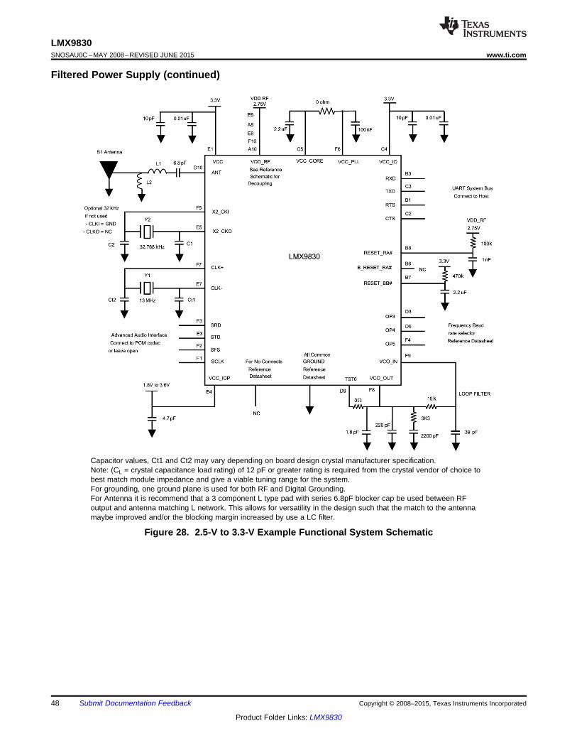
LMX9830SNOSAU0C –MAY 2008–REVISED JUNE 2015 www.ti.com
Filtered Power Supply (continued)
Capacitor values, Ct1 and Ct2 may vary depending on board design crystal manufacturer specification.Note: (CL = crystal capacitance load rating) of 12 pF or greater rating is required from the crystal vendor of choice tobest match module impedance and give a viable tuning range for the system.For grounding, one ground plane is used for both RF and Digital Grounding.For Antenna it is recommend that a 3 component L type pad with series 6.8pF blocker cap be used between RFoutput and antenna matching L network. This allows for versatility in the design such that the match to the antennamaybe improved and/or the blocking margin increased by use a LC filter.
Figure 28. 2.5-V to 3.3-V Example Functional System Schematic
48 Submit Documentation Feedback Copyright © 2008–2015, Texas Instruments Incorporated
Product Folder Links: LMX9830

LMX9830www.ti.com SNOSAU0C –MAY 2008–REVISED JUNE 2015
Filtered Power Supply (continued)
Capacitor values, Ct1 and Ct2 may vary depending on board design crystal manufacturer specification.Note: (CL = crystal capacitance load rating) of 12 pF or greater rating is required from the crystal vendor of choice tobest match module impedance and give a viable tuning range for the system.For grounding, one ground plane is used for both RF and Digital Grounding.For Antenna, TI recommends that a 3-component L type pad with series 6.8-pF blocker cap be used between RFoutput and antenna matching L network as shown above. This allows for versatility in the design such that the matchto the antenna maybe improved and/or the blocking margin increased by use a LC filter.
Figure 29. 1.8-V Example Functional System Schematic
Copyright © 2008–2015, Texas Instruments Incorporated Submit Documentation Feedback 49
Product Folder Links: LMX9830

LMX9830SNOSAU0C –MAY 2008–REVISED JUNE 2015 www.ti.com
12 Device and Documentation Support
12.1 Device SupportLMX9830 Software User’s Guide, SNWC001
LMX9830DONGLE Evaluation Module, http://www.ti.com/tool/lmx9830dongle
12.1.1 Third-Party Products DisclaimerTI'S PUBLICATION OF INFORMATION REGARDING THIRD-PARTY PRODUCTS OR SERVICES DOES NOTCONSTITUTE AN ENDORSEMENT REGARDING THE SUITABILITY OF SUCH PRODUCTS OR SERVICESOR A WARRANTY, REPRESENTATION OR ENDORSEMENT OF SUCH PRODUCTS OR SERVICES, EITHERALONE OR IN COMBINATION WITH ANY TI PRODUCT OR SERVICE.
12.2 Documentation Support
12.2.1 Related DocumentationAN-1810 LMX9830 Design Checklist, SNOA518
12.3 Community ResourcesThe following links connect to TI community resources. Linked contents are provided "AS IS" by the respectivecontributors. They do not constitute TI specifications and do not necessarily reflect TI's views; see TI's Terms ofUse.
TI E2E™ Online Community TI's Engineer-to-Engineer (E2E) Community. Created to foster collaborationamong engineers. At e2e.ti.com, you can ask questions, share knowledge, explore ideas and helpsolve problems with fellow engineers.
Design Support TI's Design Support Quickly find helpful E2E forums along with design support tools andcontact information for technical support.
12.4 TrademarksE2E is a trademark of Texas Instruments.Bluetooth is a registered trademark of Bluetooth SIG, Inc..All other trademarks are the property of their respective owners.
12.5 Electrostatic Discharge CautionThese devices have limited built-in ESD protection. The leads should be shorted together or the device placed in conductive foamduring storage or handling to prevent electrostatic damage to the MOS gates.
12.6 GlossarySLYZ022 — TI Glossary.
This glossary lists and explains terms, acronyms, and definitions.
13 Mechanical, Packaging, and Orderable InformationThe following pages include mechanical, packaging, and orderable information. This information is the mostcurrent data available for the designated devices. This data is subject to change without notice and revision ofthis document. For browser-based versions of this data sheet, refer to the left-hand navigation.
50 Submit Documentation Feedback Copyright © 2008–2015, Texas Instruments Incorporated
Product Folder Links: LMX9830

PACKAGE OPTION ADDENDUM
www.ti.com 6-Nov-2017
Addendum-Page 1
PACKAGING INFORMATION
Orderable Device Status(1)
Package Type PackageDrawing
Pins PackageQty
Eco Plan(2)
Lead/Ball Finish(6)
MSL Peak Temp(3)
Op Temp (°C) Device Marking(4/5)
Samples
LMX9830SM/NOPB NRND NFBGA NZB 60 320 Green (RoHS& no Sb/Br)
SNAGCU Level-4-260C-72 HR -40 to 125 9830SM
LMX9830SMX/NOPB NRND NFBGA NZB 60 2500 Green (RoHS& no Sb/Br)
SNAGCU Level-4-260C-72 HR -40 to 125 9830SM
(1) The marketing status values are defined as follows:ACTIVE: Product device recommended for new designs.LIFEBUY: TI has announced that the device will be discontinued, and a lifetime-buy period is in effect.NRND: Not recommended for new designs. Device is in production to support existing customers, but TI does not recommend using this part in a new design.PREVIEW: Device has been announced but is not in production. Samples may or may not be available.OBSOLETE: TI has discontinued the production of the device.
(2) RoHS: TI defines "RoHS" to mean semiconductor products that are compliant with the current EU RoHS requirements for all 10 RoHS substances, including the requirement that RoHS substancedo not exceed 0.1% by weight in homogeneous materials. Where designed to be soldered at high temperatures, "RoHS" products are suitable for use in specified lead-free processes. TI mayreference these types of products as "Pb-Free".RoHS Exempt: TI defines "RoHS Exempt" to mean products that contain lead but are compliant with EU RoHS pursuant to a specific EU RoHS exemption.Green: TI defines "Green" to mean the content of Chlorine (Cl) and Bromine (Br) based flame retardants meet JS709B low halogen requirements of <=1000ppm threshold. Antimony trioxide basedflame retardants must also meet the <=1000ppm threshold requirement.
(3) MSL, Peak Temp. - The Moisture Sensitivity Level rating according to the JEDEC industry standard classifications, and peak solder temperature.
(4) There may be additional marking, which relates to the logo, the lot trace code information, or the environmental category on the device.
(5) Multiple Device Markings will be inside parentheses. Only one Device Marking contained in parentheses and separated by a "~" will appear on a device. If a line is indented then it is a continuationof the previous line and the two combined represent the entire Device Marking for that device.
(6) Lead/Ball Finish - Orderable Devices may have multiple material finish options. Finish options are separated by a vertical ruled line. Lead/Ball Finish values may wrap to two lines if the finishvalue exceeds the maximum column width.
Important Information and Disclaimer:The information provided on this page represents TI's knowledge and belief as of the date that it is provided. TI bases its knowledge and belief on informationprovided by third parties, and makes no representation or warranty as to the accuracy of such information. Efforts are underway to better integrate information from third parties. TI has taken andcontinues to take reasonable steps to provide representative and accurate information but may not have conducted destructive testing or chemical analysis on incoming materials and chemicals.TI and TI suppliers consider certain information to be proprietary, and thus CAS numbers and other limited information may not be available for release.
In no event shall TI's liability arising out of such information exceed the total purchase price of the TI part(s) at issue in this document sold by TI to Customer on an annual basis.

PACKAGE OPTION ADDENDUM
www.ti.com 6-Nov-2017
Addendum-Page 2

TAPE AND REEL INFORMATION
*All dimensions are nominal
Device PackageType
PackageDrawing
Pins SPQ ReelDiameter
(mm)
ReelWidth
W1 (mm)
A0(mm)
B0(mm)
K0(mm)
P1(mm)
W(mm)
Pin1Quadrant
LMX9830SMX/NOPB NFBGA NZB 60 2500 330.0 16.4 6.4 9.4 2.3 8.0 16.0 Q2
PACKAGE MATERIALS INFORMATION
www.ti.com 21-Nov-2016
Pack Materials-Page 1

*All dimensions are nominal
Device Package Type Package Drawing Pins SPQ Length (mm) Width (mm) Height (mm)
LMX9830SMX/NOPB NFBGA NZB 60 2500 367.0 367.0 38.0
PACKAGE MATERIALS INFORMATION
www.ti.com 21-Nov-2016
Pack Materials-Page 2

MECHANICAL DATA
NZB0060A
www.ti.com
SLF60A (Rev A)

IMPORTANT NOTICE
Texas Instruments Incorporated (TI) reserves the right to make corrections, enhancements, improvements and other changes to itssemiconductor products and services per JESD46, latest issue, and to discontinue any product or service per JESD48, latest issue. Buyersshould obtain the latest relevant information before placing orders and should verify that such information is current and complete.TI’s published terms of sale for semiconductor products (http://www.ti.com/sc/docs/stdterms.htm) apply to the sale of packaged integratedcircuit products that TI has qualified and released to market. Additional terms may apply to the use or sale of other types of TI products andservices.Reproduction of significant portions of TI information in TI data sheets is permissible only if reproduction is without alteration and isaccompanied by all associated warranties, conditions, limitations, and notices. TI is not responsible or liable for such reproduceddocumentation. Information of third parties may be subject to additional restrictions. Resale of TI products or services with statementsdifferent from or beyond the parameters stated by TI for that product or service voids all express and any implied warranties for theassociated TI product or service and is an unfair and deceptive business practice. TI is not responsible or liable for any such statements.Buyers and others who are developing systems that incorporate TI products (collectively, “Designers”) understand and agree that Designersremain responsible for using their independent analysis, evaluation and judgment in designing their applications and that Designers havefull and exclusive responsibility to assure the safety of Designers' applications and compliance of their applications (and of all TI productsused in or for Designers’ applications) with all applicable regulations, laws and other applicable requirements. Designer represents that, withrespect to their applications, Designer has all the necessary expertise to create and implement safeguards that (1) anticipate dangerousconsequences of failures, (2) monitor failures and their consequences, and (3) lessen the likelihood of failures that might cause harm andtake appropriate actions. Designer agrees that prior to using or distributing any applications that include TI products, Designer willthoroughly test such applications and the functionality of such TI products as used in such applications.TI’s provision of technical, application or other design advice, quality characterization, reliability data or other services or information,including, but not limited to, reference designs and materials relating to evaluation modules, (collectively, “TI Resources”) are intended toassist designers who are developing applications that incorporate TI products; by downloading, accessing or using TI Resources in anyway, Designer (individually or, if Designer is acting on behalf of a company, Designer’s company) agrees to use any particular TI Resourcesolely for this purpose and subject to the terms of this Notice.TI’s provision of TI Resources does not expand or otherwise alter TI’s applicable published warranties or warranty disclaimers for TIproducts, and no additional obligations or liabilities arise from TI providing such TI Resources. TI reserves the right to make corrections,enhancements, improvements and other changes to its TI Resources. TI has not conducted any testing other than that specificallydescribed in the published documentation for a particular TI Resource.Designer is authorized to use, copy and modify any individual TI Resource only in connection with the development of applications thatinclude the TI product(s) identified in such TI Resource. NO OTHER LICENSE, EXPRESS OR IMPLIED, BY ESTOPPEL OR OTHERWISETO ANY OTHER TI INTELLECTUAL PROPERTY RIGHT, AND NO LICENSE TO ANY TECHNOLOGY OR INTELLECTUAL PROPERTYRIGHT OF TI OR ANY THIRD PARTY IS GRANTED HEREIN, including but not limited to any patent right, copyright, mask work right, orother intellectual property right relating to any combination, machine, or process in which TI products or services are used. Informationregarding or referencing third-party products or services does not constitute a license to use such products or services, or a warranty orendorsement thereof. Use of TI Resources may require a license from a third party under the patents or other intellectual property of thethird party, or a license from TI under the patents or other intellectual property of TI.TI RESOURCES ARE PROVIDED “AS IS” AND WITH ALL FAULTS. TI DISCLAIMS ALL OTHER WARRANTIES ORREPRESENTATIONS, EXPRESS OR IMPLIED, REGARDING RESOURCES OR USE THEREOF, INCLUDING BUT NOT LIMITED TOACCURACY OR COMPLETENESS, TITLE, ANY EPIDEMIC FAILURE WARRANTY AND ANY IMPLIED WARRANTIES OFMERCHANTABILITY, FITNESS FOR A PARTICULAR PURPOSE, AND NON-INFRINGEMENT OF ANY THIRD PARTY INTELLECTUALPROPERTY RIGHTS. TI SHALL NOT BE LIABLE FOR AND SHALL NOT DEFEND OR INDEMNIFY DESIGNER AGAINST ANY CLAIM,INCLUDING BUT NOT LIMITED TO ANY INFRINGEMENT CLAIM THAT RELATES TO OR IS BASED ON ANY COMBINATION OFPRODUCTS EVEN IF DESCRIBED IN TI RESOURCES OR OTHERWISE. IN NO EVENT SHALL TI BE LIABLE FOR ANY ACTUAL,DIRECT, SPECIAL, COLLATERAL, INDIRECT, PUNITIVE, INCIDENTAL, CONSEQUENTIAL OR EXEMPLARY DAMAGES INCONNECTION WITH OR ARISING OUT OF TI RESOURCES OR USE THEREOF, AND REGARDLESS OF WHETHER TI HAS BEENADVISED OF THE POSSIBILITY OF SUCH DAMAGES.Unless TI has explicitly designated an individual product as meeting the requirements of a particular industry standard (e.g., ISO/TS 16949and ISO 26262), TI is not responsible for any failure to meet such industry standard requirements.Where TI specifically promotes products as facilitating functional safety or as compliant with industry functional safety standards, suchproducts are intended to help enable customers to design and create their own applications that meet applicable functional safety standardsand requirements. Using products in an application does not by itself establish any safety features in the application. Designers mustensure compliance with safety-related requirements and standards applicable to their applications. Designer may not use any TI products inlife-critical medical equipment unless authorized officers of the parties have executed a special contract specifically governing such use.Life-critical medical equipment is medical equipment where failure of such equipment would cause serious bodily injury or death (e.g., lifesupport, pacemakers, defibrillators, heart pumps, neurostimulators, and implantables). Such equipment includes, without limitation, allmedical devices identified by the U.S. Food and Drug Administration as Class III devices and equivalent classifications outside the U.S.TI may expressly designate certain products as completing a particular qualification (e.g., Q100, Military Grade, or Enhanced Product).Designers agree that it has the necessary expertise to select the product with the appropriate qualification designation for their applicationsand that proper product selection is at Designers’ own risk. Designers are solely responsible for compliance with all legal and regulatoryrequirements in connection with such selection.Designer will fully indemnify TI and its representatives against any damages, costs, losses, and/or liabilities arising out of Designer’s non-compliance with the terms and provisions of this Notice.
Mailing Address: Texas Instruments, Post Office Box 655303, Dallas, Texas 75265Copyright © 2017, Texas Instruments Incorporated