LMX2470 2.6 GHz Delta-SigmaFractional-NPLL with 800 MHz ...
40
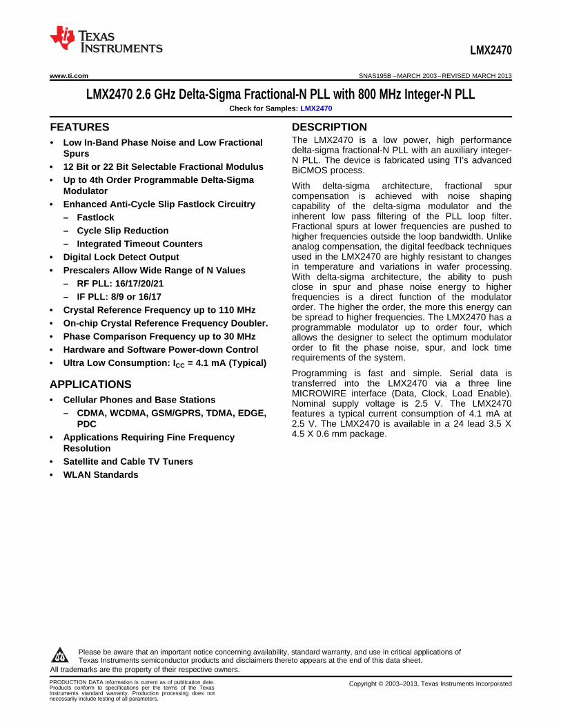
LMX2470 www.ti.com SNAS195B – MARCH 2003 – REVISED MARCH 2013 LMX2470 2.6 GHz Delta-Sigma Fractional-N PLL with 800 MHz Integer-N PLL Check for Samples: LMX2470 1FEATURES DESCRIPTION The LMX2470 is a low power, high performance 2• Low In-Band Phase Noise and Low Fractional delta-sigma fractional-N PLL with an auxiliary integer- Spurs N PLL. The device is fabricated using TI’s advanced • 12 Bit or 22 Bit Selectable Fractional Modulus BiCMOS process. • Up to 4th Order Programmable Delta-Sigma With delta-sigma architecture, fractional spur Modulator compensation is achieved with noise shaping • Enhanced Anti-Cycle Slip Fastlock Circuitry capability of the delta-sigma modulator and the inherent low pass filtering of the PLL loop filter. – Fastlock Fractional spurs at lower frequencies are pushed to – Cycle Slip Reduction higher frequencies outside the loop bandwidth. Unlike – Integrated Timeout Counters analog compensation, the digital feedback techniques used in the LMX2470 are highly resistant to changes • Digital Lock Detect Output in temperature and variations in wafer processing. • Prescalers Allow Wide Range of N Values With delta-sigma architecture, the ability to push – RF PLL: 16/17/20/21 close in spur and phase noise energy to higher – IF PLL: 8/9 or 16/17 frequencies is a direct function of the modulator order. The higher the order, the more this energy can • Crystal Reference Frequency up to 110 MHz be spread to higher frequencies. The LMX2470 has a • On-chip Crystal Reference Frequency Doubler. programmable modulator up to order four, which • Phase Comparison Frequency up to 30 MHz allows the designer to select the optimum modulator order to fit the phase noise, spur, and lock time • Hardware and Software Power-down Control requirements of the system. • Ultra Low Consumption: I CC = 4.1 mA (Typical) Programming is fast and simple. Serial data is transferred into the LMX2470 via a three line APPLICATIONS MICROWIRE interface (Data, Clock, Load Enable). • Cellular Phones and Base Stations Nominal supply voltage is 2.5 V. The LMX2470 – CDMA, WCDMA, GSM/GPRS, TDMA, EDGE, features a typical current consumption of 4.1 mA at 2.5 V. The LMX2470 is available in a 24 lead 3.5 X PDC 4.5 X 0.6 mm package. • Applications Requiring Fine Frequency Resolution • Satellite and Cable TV Tuners • WLAN Standards 1 Please be aware that an important notice concerning availability, standard warranty, and use in critical applications of Texas Instruments semiconductor products and disclaimers thereto appears at the end of this data sheet. 2All trademarks are the property of their respective owners. PRODUCTION DATA information is current as of publication date. Copyright © 2003–2013, Texas Instruments Incorporated Products conform to specifications per the terms of the Texas Instruments standard warranty. Production processing does not necessarily include testing of all parameters.
Transcript of LMX2470 2.6 GHz Delta-SigmaFractional-NPLL with 800 MHz ...
LMX2470
www.ti.com SNAS195B –MARCH 2003–REVISED MARCH 2013
LMX2470 2.6 GHz Delta-Sigma Fractional-N PLL with 800 MHz Integer-N PLLCheck for Samples: LMX2470
1FEATURES DESCRIPTIONThe LMX2470 is a low power, high performance
2• Low In-Band Phase Noise and Low Fractionaldelta-sigma fractional-N PLL with an auxiliary integer-SpursN PLL. The device is fabricated using TI’s advanced
• 12 Bit or 22 Bit Selectable Fractional Modulus BiCMOS process.• Up to 4th Order Programmable Delta-Sigma
With delta-sigma architecture, fractional spurModulator compensation is achieved with noise shaping• Enhanced Anti-Cycle Slip Fastlock Circuitry capability of the delta-sigma modulator and the
inherent low pass filtering of the PLL loop filter.– FastlockFractional spurs at lower frequencies are pushed to– Cycle Slip Reductionhigher frequencies outside the loop bandwidth. Unlike
– Integrated Timeout Counters analog compensation, the digital feedback techniquesused in the LMX2470 are highly resistant to changes• Digital Lock Detect Outputin temperature and variations in wafer processing.• Prescalers Allow Wide Range of N ValuesWith delta-sigma architecture, the ability to push
– RF PLL: 16/17/20/21 close in spur and phase noise energy to higher– IF PLL: 8/9 or 16/17 frequencies is a direct function of the modulator
order. The higher the order, the more this energy can• Crystal Reference Frequency up to 110 MHzbe spread to higher frequencies. The LMX2470 has a
• On-chip Crystal Reference Frequency Doubler. programmable modulator up to order four, which• Phase Comparison Frequency up to 30 MHz allows the designer to select the optimum modulator
order to fit the phase noise, spur, and lock time• Hardware and Software Power-down Controlrequirements of the system.• Ultra Low Consumption: ICC = 4.1 mA (Typical)Programming is fast and simple. Serial data istransferred into the LMX2470 via a three lineAPPLICATIONSMICROWIRE interface (Data, Clock, Load Enable).
• Cellular Phones and Base Stations Nominal supply voltage is 2.5 V. The LMX2470– CDMA, WCDMA, GSM/GPRS, TDMA, EDGE, features a typical current consumption of 4.1 mA at
2.5 V. The LMX2470 is available in a 24 lead 3.5 XPDC4.5 X 0.6 mm package.• Applications Requiring Fine Frequency
Resolution• Satellite and Cable TV Tuners• WLAN Standards
1
Please be aware that an important notice concerning availability, standard warranty, and use in critical applications ofTexas Instruments semiconductor products and disclaimers thereto appears at the end of this data sheet.
2All trademarks are the property of their respective owners.
PRODUCTION DATA information is current as of publication date. Copyright © 2003–2013, Texas Instruments IncorporatedProducts conform to specifications per the terms of the TexasInstruments standard warranty. Production processing does notnecessarily include testing of all parameters.
LMX2470
SNAS195B –MARCH 2003–REVISED MARCH 2013 www.ti.com
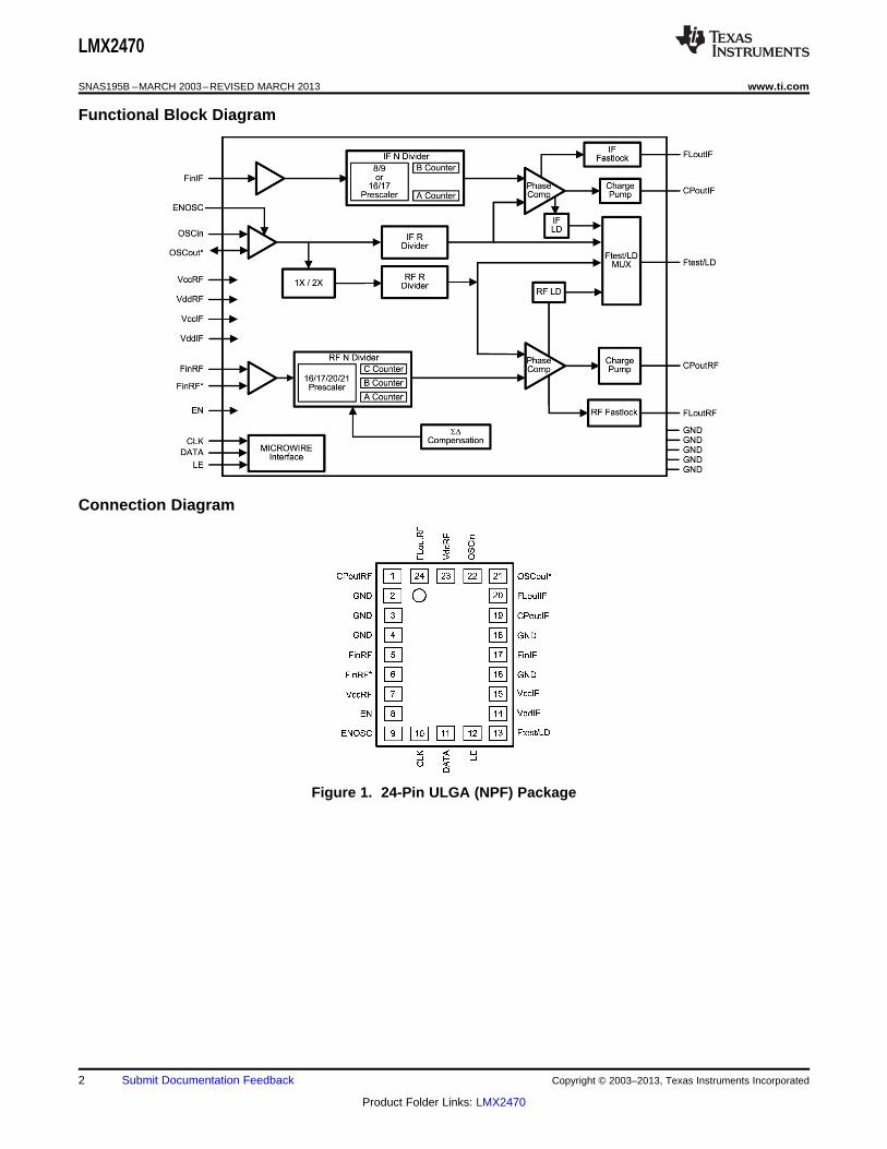
Functional Block Diagram
Connection Diagram
Figure 1. 24-Pin ULGA (NPF) Package
2 Submit Documentation Feedback Copyright © 2003–2013, Texas Instruments Incorporated
Product Folder Links: LMX2470

LMX2470
www.ti.com SNAS195B –MARCH 2003–REVISED MARCH 2013
PIN DESCRIPTIONSPin # Pin Name I/O Pin Description
1 CPoutRF O RF charge pump output.
2 GND - Ground
3 GND - RF Ground
4 GND - Ground for RF PLL digital circuitry.
5 FinRF I RF prescaler input. Small signal input from the VCO.
6 FinRF* I RF prescaler complimentary input. For single-ended operation, a bypass capacitor should be placedas close as possible to this pin and be connected directly to the ground plane.
7 VccRF RF PLL power supply voltage input. Must be equal to VccIF . May range from 2.25V to 2.75V.Bypass capacitors should be placed as close as possible to this pin and be connected directly to theground plane.
8 EN I Chip enable input. High impedance CMOS input. When EN is high, the chip is powered up, otherwiseit is powered down.
9 ENOSC I This pin should be grounded for normal operation.
10 CLK I MICROWIRE Clock. High impedance CMOS Clock input. Data for the various counters is clockedinto the 24 bit shift register on the rising edge.
11 DATA I MICROWIRE Data. High impedance binary serial data input.
12 LE MICROWIRE Load Enable. High impedance CMOS input. Data stored in the shift registers is loadedinto the internal latches when LE goes HIGH
13 Ftest/LD O Test frequency output / Lock Detect
14 VddIF - Digital power supply for IF PLL
15 VccIF - IF power supply voltage input. Must be equal to VccRF. Input may range from 2.25 V to 2.75 V.Bypass capacitors should be placed as close as possible to this pin and be connected directly to theground plane.
16 GND - Ground for RF PLL digital circuitry.
17 FinIF I IF prescaler input. Small signal input from the VCO.
18 GND - Digital ground for IF PLL
19 CPoutIF O IF PLL charge pump output
20 FLoutIF O IF Fastlock Output. Also functions as Programmable TRI-STATE CMOS output.
21 OSCout* I/O Complementary reference input or oscillator output.
22 OSCin I Reference input
23 VddRF - Digital power supply for RF PLL
24 FLoutRF O RF Fastlock Output. Also functions as Programmable TRI-STATE CMOS output.
Copyright © 2003–2013, Texas Instruments Incorporated Submit Documentation Feedback 3
Product Folder Links: LMX2470

LMX2470
SNAS195B –MARCH 2003–REVISED MARCH 2013 www.ti.com
These devices have limited built-in ESD protection. The leads should be shorted together or the device placed in conductive foamduring storage or handling to prevent electrostatic damage to the MOS gates.
Absolute Maximum Ratings (1) (2)
ValueParameter Symbol Units
Min Typ Max
Power Supply Voltage VCC -0.3 3.0 V
VDD VCC VCC V
Voltage on any pin with GND =VSS = 0V Vi -0.3 VCC + 0.3 V
Storage Temperature Range Ts -65 +150 °C
Lead Temperature (Solder 4 sec.) TL +260 °C
(1) “Absolute Maximum Ratings” indicate limits beyond which damage to the device may occur. "Recommended Operating Conditions"indicate conditions for which the device is intended to be functional, but do not ensure specific performance limits. For ensuredspecifications and test conditions, see the Electrical Characteristics. The ensured specifications apply only for the test conditions listed.Note also that these maximum ratings imply that the voltage at all the power supply pins of VccRF, VccIF, VddRF, and VddIF are thesame. VCCwill be used to refer to the voltage at these pins.
(2) This Device is a high performance RF integrated circuit with an ESD rating < 2 kV and is ESD sensitive. Handling and assembly of thisdevice should only be done at ESD-free workstations.
Recommended Operating ConditionsValue
Parameter Symbol UnitsMin Typ Max
Power Supply Voltage (1) VCC 2.25 2.75 V
VDD VCC VCC V
Operating Temperature TA -40 +85 °C
(1) “Absolute Maximum Ratings” indicate limits beyond which damage to the device may occur. "Recommended Operating Conditions"indicate conditions for which the device is intended to be functional, but do not ensure specific performance limits. For ensuredspecifications and test conditions, see the Electrical Characteristics. The ensured specifications apply only for the test conditions listed.Note also that these maximum ratings imply that the voltage at all the power supply pins of VccRF, VccIF, VddRF, and VddIF are thesame. VCCwill be used to refer to the voltage at these pins.
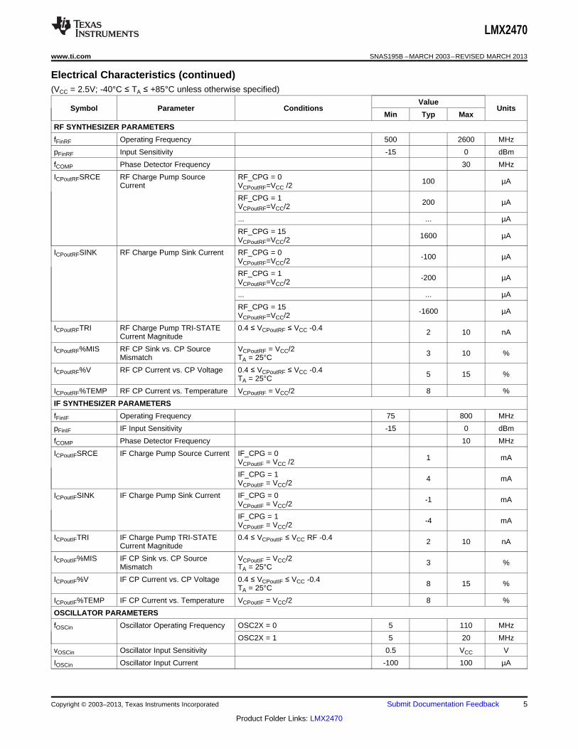
Electrical Characteristics(VCC = 2.5V; -40°C ≤ TA ≤ +85°C unless otherwise specified)
ValueSymbol Parameter Conditions Units
Min Typ Max
Icc PARAMETERS
ICCRF Power Supply Current, RF IF PLL OFFSynthesizer RF PLL ON 2.7 3.9 mACharge Pump TRI-STATE
OSC=0
ICCIF Power Supply Current, IF IF PLL ONSynthesizer RF PLL OFF 1.4 2.3 mACharge Pump TRI-STATE
OSC=0
ICCTOTAL Power Supply Current, Entire IF PLL ONSynthesizer RF PLL ON 4.1 6.0 mACharge Pump TRI-STATE
OSC=0
ICCPD Power Down Current EN = ENOSC = 0V 1 10 µACLK, DATA, LE = 0V
4 Submit Documentation Feedback Copyright © 2003–2013, Texas Instruments Incorporated
Product Folder Links: LMX2470
LMX2470
www.ti.com SNAS195B –MARCH 2003–REVISED MARCH 2013
Electrical Characteristics (continued)(VCC = 2.5V; -40°C ≤ TA ≤ +85°C unless otherwise specified)
ValueSymbol Parameter Conditions Units
Min Typ Max
RF SYNTHESIZER PARAMETERS
fFinRF Operating Frequency 500 2600 MHz
pFinRF Input Sensitivity -15 0 dBm
fCOMP Phase Detector Frequency 30 MHz
ICPoutRFSRCE RF Charge Pump Source RF_CPG = 0 100 µACurrent VCPoutRF=VCC /2
RF_CPG = 1 200 µAVCPoutRF=VCC/2
... ... µA
RF_CPG = 15 1600 µAVCPoutRF=VCC/2
ICPoutRFSINK RF Charge Pump Sink Current RF_CPG = 0 -100 µAVCPoutRF=VCC/2
RF_CPG = 1 -200 µAVCPoutRF=VCC/2
... ... µA
RF_CPG = 15 -1600 µAVCPoutRF=VCC/2
ICPoutRFTRI RF Charge Pump TRI-STATE 0.4 ≤ VCPoutRF ≤ VCC -0.4 2 10 nACurrent Magnitude
ICPoutRF%MIS RF CP Sink vs. CP Source VCPoutRF = VCC/2 3 10 %Mismatch TA = 25°C
ICPoutRF%V RF CP Current vs. CP Voltage 0.4 ≤ VCPoutRF ≤ VCC -0.4 5 15 %TA = 25°C
ICPoutRF%TEMP RF CP Current vs. Temperature VCPoutRF = VCC/2 8 %
IF SYNTHESIZER PARAMETERS
fFinIF Operating Frequency 75 800 MHz
pFinIF IF Input Sensitivity -15 0 dBm
fCOMP Phase Detector Frequency 10 MHz
ICPoutIFSRCE IF Charge Pump Source Current IF_CPG = 0 1 mAVCPoutIF = VCC /2
IF_CPG = 1 4 mAVCPoutIF = VCC/2
ICPoutIFSINK IF Charge Pump Sink Current IF_CPG = 0 -1 mAVCPoutIF = VCC/2
IF_CPG = 1 -4 mAVCPoutIF = VCC/2
ICPoutIFTRI IF Charge Pump TRI-STATE 0.4 ≤ VCPoutIF ≤ VCC RF -0.4 2 10 nACurrent Magnitude
ICPoutIF%MIS IF CP Sink vs. CP Source VCPoutIF = VCC/2 3 %Mismatch TA = 25°C
ICPoutIF%V IF CP Current vs. CP Voltage 0.4 ≤ VCPoutIF ≤ VCC -0.4 8 15 %TA = 25°C
ICPoutIF%TEMP IF CP Current vs. Temperature VCPoutIF = VCC/2 8 %
OSCILLATOR PARAMETERS
fOSCin Oscillator Operating Frequency OSC2X = 0 5 110 MHz
OSC2X = 1 5 20 MHz
vOSCin Oscillator Input Sensitivity 0.5 VCC V
IOSCin Oscillator Input Current -100 100 µA
Copyright © 2003–2013, Texas Instruments Incorporated Submit Documentation Feedback 5
Product Folder Links: LMX2470

LMX2470
SNAS195B –MARCH 2003–REVISED MARCH 2013 www.ti.com
Electrical Characteristics (continued)(VCC = 2.5V; -40°C ≤ TA ≤ +85°C unless otherwise specified)
ValueSymbol Parameter Conditions Units
Min Typ Max
DIGITAL INTERFACE (DATA, CLK, LE, EN, ENRF, Ftest/LD, FLoutRF, FLoutIF)
VIH High-Level Input Voltage 1.6 VCC V
VIL Low-Level Input Voltage 0.4 V
IIH High-Level Input Current VIH = VCC -1.0 1.0 µA
IIL Low-Level Input Current VIL = 0 V -1.0 1.0 µA
VOH High-Level Output Voltage IOH = -500 µA VCC-0.4 V
VOL Low-Level Output Voltage IOL = 500 µA 0.4 V
MICROWIRE INTERFACE TIMING
TCS Data to Clock Set Up Time See MICROWIRE INPUT TIMING 50 nsDIAGRAM
TCH Data to Clock Hold Time See MICROWIRE INPUT TIMING 10 nsDIAGRAM
TCWH Clock Pulse Width High See MICROWIRE INPUT TIMING 50 nsDIAGRAM
TCWL Clock Pulse Width Low See MICROWIRE INPUT TIMING 50 nsDIAGRAM
TES Clock to Load Enable Set Up See MICROWIRE INPUT TIMING 50 nsTime DIAGRAM
TEW Load Enable Pulse Width See MICROWIRE INPUT TIMING 50 nsDIAGRAM
PHASE NOISE
LF1HzRF RF Synthesizer Normalized RF_CPG = 0 -200 dBc/HzPhase Noise Contribution (1)
RF_CPG = 3 -206 dBc/Hz
RF_CPG = 7 -208 dBc/Hz
RF_CPG = 15 -210 dBc/Hz
LF1HzIF IF Synthesizer Normalized Applies to both low and high current -209 dBc/HzPhase Noise Contribution (1) modes
(1) Normalized Phase Noise Contribution is defined as: LN(f) = L(f) – 20log(N) – 10log(fCOMP) where L(f) is defined as the single side bandphase noise measured at an offset frequency, f, in a 1 Hz Bandwidth. The offset frequency, f, must be chosen sufficiently smaller thanthe PLL loop bandwidth, yet large enough to avoid substantial phase noise contribution from the reference source. The offset chosenwas 4 KHz.
MICROWIRE INPUT TIMING DIAGRAM
6 Submit Documentation Feedback Copyright © 2003–2013, Texas Instruments Incorporated
Product Folder Links: LMX2470

LMX2470
www.ti.com SNAS195B –MARCH 2003–REVISED MARCH 2013
Typical Performance Characteristics: Sensitivity
RF N Counter Sensitivity RF N Counter SensitivityTA = 25°C VCC = 2.5 V
Figure 2. Figure 3.
IF N Counter Sensitivity IF N Counter SensitivityTA = 25°C VCC = 2.5 V
Figure 4. Figure 5.
OSCin Counter Sensitivity OSCin Counter SensitivityOSC=0 OSC=0
TA = 25°C VCC= 2.5 V
Figure 6. Figure 7.
Copyright © 2003–2013, Texas Instruments Incorporated Submit Documentation Feedback 7
Product Folder Links: LMX2470

LMX2470
SNAS195B –MARCH 2003–REVISED MARCH 2013 www.ti.com
Typical Performance Characteristics: FinRF Input Impedance
Figure 8.
FinRF Input Impedance
Frequency (MHz) Real (Ohms) Imaginary (Ohms)
500 214 -255
600 175 -245
700 144 -230
800 118 -216
900 98 -203
1000 80 -189
1100 69 -177
1200 57 -165
1300 48 -153
1400 39 -141
1500 34 -130
1600 28 -119
1700 24 -110
1800 20 -101
1900 17 -94
2000 14 -87
2100 13 -82
2200 11 -77
2300 10 -72
2400 8 -67
2500 7 -62
2600 7 -56
2700 7 -53
2800 7 -46
2900 7 -41
3000 7 -39
8 Submit Documentation Feedback Copyright © 2003–2013, Texas Instruments Incorporated
Product Folder Links: LMX2470

LMX2470
www.ti.com SNAS195B –MARCH 2003–REVISED MARCH 2013
Typical Performance Characteristics: FinIF Input Impedance
Figure 9.
FinIF Input Impedance
Freqeuncy (MHz) Real (Ohms) Imaginary (Ohms)
50 580 -313
100 500 -273
150 445 -250
200 410 -256
250 378 -259
300 349 -264
350 322 -267
400 297 -270
450 274 -271
500 253 -272
550 232 -272
600 214 -269
650 198 -265
700 184 -262
750 170 -259
800 157 -256
900 151 -253
1000 143 -250
Copyright © 2003–2013, Texas Instruments Incorporated Submit Documentation Feedback 9
Product Folder Links: LMX2470

LMX2470
SNAS195B –MARCH 2003–REVISED MARCH 2013 www.ti.com
Typical Performance Characteristics: OSCin Input Impedance
Figure 10.
OSCin Input Impedance
Frequency (MHz) Real (Ohms) Imaginary (Ohms) Magnitude (Ohms)
50 2200 -4700 5189
10 710 -2700 2792
20 229 -1500 1517
30 133 -988 997
40 93 -752 758
50 74 -606 611
60 62 -505 509
70 53 -435 438
80 49 -382 385
90 45 -341 344
100 42 -309 312
110 40 -282 285
10 Submit Documentation Feedback Copyright © 2003–2013, Texas Instruments Incorporated
Product Folder Links: LMX2470

LMX2470
www.ti.com SNAS195B –MARCH 2003–REVISED MARCH 2013
Typical Performance Characteristics: Currents
Total Current Consumption Powerdown CurrentOSC=0 EN = LOW
Figure 11. Figure 12.
RF Charge Pump Current IF Charge Pump CurrentVCC = 2.5 Volts VCC = 2.5 Volts
Figure 13. Figure 14.
Charge Pump Leakage Charge Pump LeakageRF PLL IF PLL
Typical performance characteristics do not imply any sort of ensuredspecification. Ensured specifications are in the ElectricalCharacteristics.
Figure 15. Figure 16.
Copyright © 2003–2013, Texas Instruments Incorporated Submit Documentation Feedback 11
Product Folder Links: LMX2470

LMX2470
SNAS195B –MARCH 2003–REVISED MARCH 2013 www.ti.com
BENCH TEST SETUPS
Charge Pump Current Measurement Procedure
The above block diagram shows the test procedure for testing the RF and IF charge pumps. These tests includeabsolute current level, mismatch, and leakage. In order to measure the charge pump currents, a signal is appliedto the high frequency input pins. The reason for this is to ensure that the phase detector gets enough transitionsin order to be able to change states. If no signal is applied, it is possible that the charge pump current readingwill be low due to the fact that the duty cycle is not 100%. The OSCin Pin is tied to the supply. The charge pumpcurrents can be measured by simply programming the phase detector to the necessary polarity. For instance, inorder to measure the RF charge pump current, a 10 MHz signal is applied to the FinRF pin. The source currentcan be measured by setting the RF PLL phase detector to a positive polarity, and the sink current can bemeasured by setting the phase detector to a negative polarity. The IF PLL currents can be measured in a similarway. Note that the magnitude of the RF and IF PLL charge pump currents are also controlled by the RF_CPGand IF_CPG bits. Once the charge pump currents are known, the mismatch can be calculated as well. In order tomeasure leakage currents, the charge pump current is set to a TRI-STATE mode by enabling the counter resetbits. This is RF_RST for the RF PLL and IF_RST for the IF PLL. The table below shows a summary of thevarious charge pump tests.
Current Test RF_CPG RF_CPP RF_CPT IF_CPG IF_CPP IF_CPT
RF Source 0 to 15 0 0 X X X
RF Sink 0 to 15 1 0 X X X
RF TRI-STATE X X 1 X X X
IF Source X X X 0 to 1 0 0
IF Sink X X X 0 to 1 1 0
IF TRI-STATE X X X X X 1
12 Submit Documentation Feedback Copyright © 2003–2013, Texas Instruments Incorporated
Product Folder Links: LMX2470

LMX2470
www.ti.com SNAS195B –MARCH 2003–REVISED MARCH 2013
Frequency Input Pin DC Blocking Corresponding Default Counter MUX Value OSCCapacitor Counter Value
OSCin 1000 pF RF_R / 2 50 14 0
FinRF 100 pF RF_N / 2 500 15 X
FinIF 100 pF IF_N / 2 500 13 X
Sensitivity Measurement Procedure
Sensitivity is defined as the power level limits beyond which the output of the counter being tested is off by 1 Hzor more of its expected value. It is typically measured over frequency, voltage, and temperature. In order to testsensitivity, the MUX[3:0] word is programmed to the appropriate value. The counter value is then programmed toa fixed value and a frequency counter is set to monitor the frequency of this pin. The expected frequency at theFtest/LD pin should be the signal generator frequency divided by twice the corresponding counter value. Thefactor of two comes in because the LMX2470 has a flip-flop which divides this frequency by two to make the dutycycle 50% in order to make it easier to read with the frequency counter. The frequency counter input impedanceshould be set to high impedance. In order to perform the measurement, the temperature, frequency, and voltageis set to a fixed value and the power level of the signal is varied. Note that the power level at the part is assumedto be 4 dB less than the signal generator power level. This accounts for 1 dB for cable losses and 3 dB for thepad. The power level range where the frequency is correct at the Ftest/LD pin to within 1 Hz accuracy isrecorded for the sensitivity limits. The temperature, frequency, and voltage can be varied in order to produce afamily of sensitivity curves. Since this is an open-loop test, the charge pump is set to TRI-STATE and the unusedside of the PLL (RF or IF) is powered down when not being tested. For this part, there are actually four frequencyinput pins, although there is only one frequency test pin (Ftest/LD). The conditions specific to each pin are showabove.
Copyright © 2003–2013, Texas Instruments Incorporated Submit Documentation Feedback 13
Product Folder Links: LMX2470

LMX2470
SNAS195B –MARCH 2003–REVISED MARCH 2013 www.ti.com
Input Impedance Measurement Procedure
The above block diagram shows the test procedure measuring the input impedance for the LMX2470. Thisapplies to the FinRF, FinIF, and OSCin pins. The basic test procedure is to calibrate the network analyzer,ensure that the part is powered up, and then measure the input impedance. The network analyzer can becalibrated by using either calibration standards or by soldering resistors directly to the evaluation board. An opencan be implemented by putting no resistor, a short can be implemented by using a 0 ohm resistor, and a shortcan be implemented by using two 100 ohm resistors in parallel. Note that no DC blocking capacitor is used forthis test procedure. This is done with the PLL removed from the PCB. This requires the use of a clamp downfixture that may not always be generally available. If no clamp down fixture is available, then this procedure canbe done by calibrating up to the point where the DC blocking capacitor usually is, and then adding a 0 ohmresistor back for the actual measurement. Once that the network analyzer is calibrated, it is necessary to ensurethat the PLL is powered up. This can be done by toggling the power down bits (RF_PD and IF_PD) andobserving that the current consumption indeed increases when the bit is disabled. Sometimes it may benecessary to apply a signal to the OSCin pin in order to program the part. If this is necessary, disconnect thesignal once it is established that the part is powered up. It is useful to know the input impedance of the PLL forthe purposes of debugging RF problems and designing matching networks. Another use of knowing thisparameter is make the trace width on the PCB such that the input impedance of this trace matches the real partof the input impedance of the PLL frequency of operation. In general, it is good practice to keep trace lengthsshort and make designs that are relatively resistant to variations in the input impedance of the PLL.
Functional Description
GENERAL
The basic phase-lock-loop (PLL) configuration consists of a high-stability crystal reference oscillator, a frequencysynthesizer such as the TI LMX2470, a voltage controlled oscillator (VCO), and a passive loop filter. Thefrequency synthesizer includes a phase detector, current mode charge pump, as well as programmablereference [R] and feedback [N] frequency dividers. The VCO frequency is established by dividing the crystalreference signal down via the R counter to obtain a frequency that sets the comparison frequency. Thiscomparison frequency, fCOMP, is input of a phase/frequency detector and compared with another signal, fN, thefeedback signal, which was obtained by dividing the VCO frequency down by way of the N counter and fractionalcircuitry. The phase/frequency detector's current source outputs a charge into the loop filter, which is thenconverted into the VCO's control voltage. The function of the phase/frequency comparator is to adjust the voltagepresented to the VCO until the frequency and phase of the feedback signal match that of the reference signal.When this ‘phase-locked’ condition exists, the VCO frequency will be N+F times that of the comparisonfrequency, where N is the integer component of the divide ratio and F is the fractional component. Fractionalsynthesis allows the phase detector frequency to be increased while maintaining the same frequency step sizefor channel selection. The division value N is thereby reduced giving a lower phase noise referred to the phasedetector input, and the comparison frequency is increased allowing faster switching times.
14 Submit Documentation Feedback Copyright © 2003–2013, Texas Instruments Incorporated
Product Folder Links: LMX2470

LMX2470
www.ti.com SNAS195B –MARCH 2003–REVISED MARCH 2013
PHASE DETECTOR OPERATING FREQUENCY
The maximum phase detector operating frequency for the LMX2470 is 30 MHz. However, this is not possible inall circumstances due to illegal divide ratios of the N counter. The crystal reference frequency also limits thephase detector frequency. There are trade-offs in choosing what phase detector frequency to operate at. If thisfrequency is run higher, then phase noise will be lower, but lock time may be increased due to cycle slipping.After this phase detector frequency gets sufficiently high, then there are diminishing returns for phase noise, andraising the charge pump current has a greater impact on phase noise. This phase detector frequency also has animpact on fractional spurs. In general, the spur performance is better at higher phase detector frequencies,although this is application specific. The current consumption may also slightly increase with higher phasedetector frequencies.
OSCILLATOR
The LMX2470 provides maximum flexibility for choosing an oscillator reference. One possible method is to use asingle-ended TCXO to drive the OSCin pin. The part can also be configured to be driven differentially using theOSCin and OSCout* pins. Note that the OSCin and OSCout* pins can not be used as an inverter for a crystal.Selection between these two modes does have a noticeable impact on phase noise and sub-fractional spurs.Regardless of which mode is used, the performance is generally best for higher oscillator power levels.
POWER DOWN AND POWER UP MODES
The power down state of the LMX2470 is controlled by many factors. The one factor that overrides all otherfactors is the EN pin. If this pin is low, this ensures the part will be powered down. Asserting a high logic level onEN is necessary to power up the chip, however, there are other bits in the programming registers that canoverride this and put the PLL back in a power down state. Provided that the voltage on the EN pin is high,programming the RF_PD and IF_PD bits to zero ensures that the part will be powered up. Programming eitherone of these bits to one will power down the appropriate section of the synthesizer, provided that the ATPU[1:0](Auto Power Up) bits do not override this.
There are many different ways to power down this chip and many different things that can be powered down.This section discusses how to power down the PLLs on the chip. There are two terms that need to be definedfirst: synchronous power down and asynchronous power down. In the case of synchronous power down, the PLLchip powers down after the charge pump turns off. This is best to prevent unwanted frequency glitches uponpower up. However, in certain cases where the charge pump is stuck on, such as the case when there is noVCO signal applied, this type of power down will not reliably work and asynchronous power down is necessary.In the case of asynchronous power down, the PLL powers down regardless of the status of the charge pump.There are 4 factors that affect the power down state of the chip: the EN pin, the power down bit, the TRI-STATEbit, and writing to the RF N counter with the RF_ATPU[1:0] bits enabled
EN Pin ATPU[1:0] Bits Enabled RF_PD Bit RF_CPT Bit PLL State+
RF N Counter Written To
Low X X X Asynchronous PowerDown
High Yes X X PLL is active with chargepump in the active state.
High No 0 0 PLL is active with chargepump in the active state.
High No 0 1 PLL is active, but chargepump is TRI-STATE.
High No 1 0 Synchronous Power Down
High No 1 1 Asynchronous PowerDown
Copyright © 2003–2013, Texas Instruments Incorporated Submit Documentation Feedback 15
Product Folder Links: LMX2470
LMX2470
SNAS195B –MARCH 2003–REVISED MARCH 2013 www.ti.com
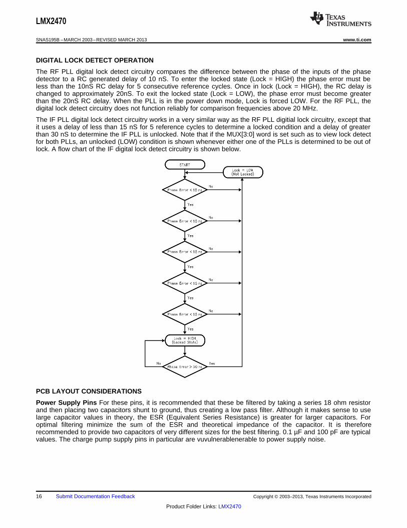
DIGITAL LOCK DETECT OPERATION
The RF PLL digital lock detect circuitry compares the difference between the phase of the inputs of the phasedetector to a RC generated delay of 10 nS. To enter the locked state (Lock = HIGH) the phase error must beless than the 10nS RC delay for 5 consecutive reference cycles. Once in lock (Lock = HIGH), the RC delay ischanged to approximately 20nS. To exit the locked state (Lock = LOW), the phase error must become greaterthan the 20nS RC delay. When the PLL is in the power down mode, Lock is forced LOW. For the RF PLL, thedigital lock detect circuitry does not function reliably for comparison frequencies above 20 MHz.
The IF PLL digital lock detect circuitry works in a very similar way as the RF PLL digitial lock circuitry, except thatit uses a delay of less than 15 nS for 5 reference cycles to determine a locked condition and a delay of greaterthan 30 nS to determine the IF PLL is unlocked. Note that if the MUX[3:0] word is set such as to view lock detectfor both PLLs, an unlocked (LOW) condition is shown whenever either one of the PLLs is determined to be out oflock. A flow chart of the IF digital lock detect circuitry is shown below.
PCB LAYOUT CONSIDERATIONS
Power Supply Pins For these pins, it is recommended that these be filtered by taking a series 18 ohm resistorand then placing two capacitors shunt to ground, thus creating a low pass filter. Although it makes sense to uselarge capacitor values in theory, the ESR (Equivalent Series Resistance) is greater for larger capacitors. Foroptimal filtering minimize the sum of the ESR and theoretical impedance of the capacitor. It is thereforerecommended to provide two capacitors of very different sizes for the best filtering. 0.1 µF and 100 pF are typicalvalues. The charge pump supply pins in particular are vuvulnerablenerable to power supply noise.
16 Submit Documentation Feedback Copyright © 2003–2013, Texas Instruments Incorporated
Product Folder Links: LMX2470
LMX2470
www.ti.com SNAS195B –MARCH 2003–REVISED MARCH 2013
High Frequency Input Pins, FinRF and FinIF The signal path from the VCO to the PLL is the most sensitiveand challenging for board layout. It is generally recommended that the VCO output go through a resistive padand then through a DC blocking capacitor before it gets to these high frequency input pins. If the trace length issufficiently short (< 1/10th of a wavelength), then the pad may not be necessary, but a series resistor of about 39ohms is still recommended to isolate the PLL from the VCO. The DC blocking capacitor should be chosen atleast to be 100 pF. It may turn out that the frequency in this trace is above the self-resonant frequency of thecapacitor, but since the input impedance of the PLL tends to be capacitive, it actually be a benefit to exceed theself-resonant frequency. The pad and the DC blocking capacitor should be placed as close to the PLL aspossible
Complimentary High Frequency Pin, FinRF* These inputs may be used to drive the PLL differentially, but it isvery common to drive the PLL in a single ended fashion. A shunt capacitor should be placed at the FinRF* pin.The value of this capacitor should be chosen such that the impedance, including the ESR of the capacitor, is asclose to an AC short as possible at the operating frequency of the PLL. 100 pF is a typical value.
FASTLOCK AND CYCLE SLIP REDUCTION
The LMX2470 has enhanced features for Fastlock and cycle slip operation. The next several sections discussthe the benefits of using both of these features. There are four possible combinations that are possible, andthese are shown in the table below:
Decrease ComparisonKeep ComparisonCharge Pump Current Frequency (CSR)Frequency the Same (RF Side Only)
Increase Charge Pump Current Classical Fastlock CSR/Fastlock CombinationAllows the loop bandwidth to be increased. Engaging the CSR does decrease the loopThis has a frequency glitch caused by bandwidth during frequency acquisition, butswitching the charge pump currents, but may be necessary to reduce cycle slipping.there is no frequency glitch caused by By also increasing the charge pump current,switching from fractional to integer mode this can compensate for the reduce loop
bandwidth due to the CSR
Keep Charge Pump Current the Same Operation with No Fastlock CSR OnlyThis mode represents using no Fastlock This mode is not generally recommended,
but may reduce cycle slipping in someapplications. Although the theoretical locktime is decreased, due to the decreased loopbandwidth during Fastlock, cycle slips can bereduced or eliminated.
Decrease Charge Pump Current It never makes sense to use a lower chargepump current during Fastlock than in thesteady state.
Note that if the charge pump current and cycle slip reduction circuitry are engaged in the same proportion, then itis not necessary to switch in a Fastlock resistor and the loop filter will be optimized for both normal mode andFastlock mode. For third and fourth order filters which have problems with cycle slipping, this may prove to bethe optimal choice of settings.
Determining the Loop Gain Multiplier, K
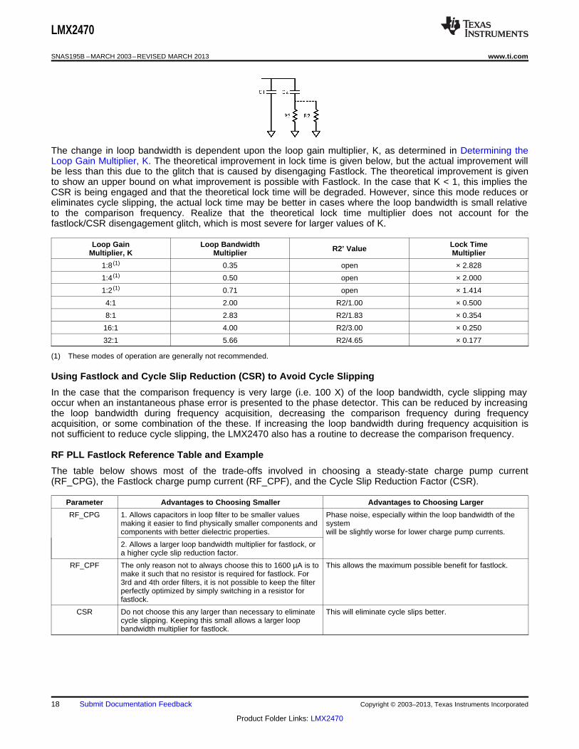
The loop bandwidth multiplier, K, is needed in order to determine the theoretical impact of fastlock/CSR on theloop bandwidth and also which resistor should be switched in parallel with the loop filter resistor R2. K = K_K ·K_Fcomp where K is the loop gain multiplier K_K is the ratio of the Fastlock charge pump current to the steadystate charge pump current. Note that this should always be greater than or equal to one. K_Fcomp is the ratio ofthe Fastlock comparison frequency to the steady state comparison frequency. If this ratio is less than one, thisimplies that the CSR is being used.
Determining the Theoretical Lock Time Improvement and Fastlock Resistor, R2’
When using fastlock, it is necessary to switch in a resistor R2’, in parallel with R2 in order to keep the loop filteroptimized and maintain the same phase margin. After the PLL has achieved a frequency that is sufficiently closeto the desired frequency, the resistor R2’ is disengaged and the charge pump current is and comparisonfrequency are returned to normal. Of special concern is the glitch that is caused when the resistor R2’ isdisengaged. This glitch can take up a significant portion of the lock time. The LMX2470 has enhanced switchingcircuitry to minimize this glitch and therefore improve the lock time.
Copyright © 2003–2013, Texas Instruments Incorporated Submit Documentation Feedback 17
Product Folder Links: LMX2470
LMX2470
SNAS195B –MARCH 2003–REVISED MARCH 2013 www.ti.com
The change in loop bandwidth is dependent upon the loop gain multiplier, K, as determined in Determining theLoop Gain Multiplier, K. The theoretical improvement in lock time is given below, but the actual improvement willbe less than this due to the glitch that is caused by disengaging Fastlock. The theoretical improvement is givento show an upper bound on what improvement is possible with Fastlock. In the case that K < 1, this implies theCSR is being engaged and that the theoretical lock time will be degraded. However, since this mode reduces oreliminates cycle slipping, the actual lock time may be better in cases where the loop bandwidth is small relativeto the comparison frequency. Realize that the theoretical lock time multiplier does not account for thefastlock/CSR disengagement glitch, which is most severe for larger values of K.
Loop Gain Loop Bandwidth Lock TimeR2’ ValueMultiplier, K Multiplier Multiplier
1:8 (1) 0.35 open × 2.828
1:4 (1) 0.50 open × 2.000
1:2 (1) 0.71 open × 1.414
4:1 2.00 R2/1.00 × 0.500
8:1 2.83 R2/1.83 × 0.354
16:1 4.00 R2/3.00 × 0.250
32:1 5.66 R2/4.65 × 0.177
(1) These modes of operation are generally not recommended.
Using Fastlock and Cycle Slip Reduction (CSR) to Avoid Cycle Slipping
In the case that the comparison frequency is very large (i.e. 100 X) of the loop bandwidth, cycle slipping mayoccur when an instantaneous phase error is presented to the phase detector. This can be reduced by increasingthe loop bandwidth during frequency acquisition, decreasing the comparison frequency during frequencyacquisition, or some combination of the these. If increasing the loop bandwidth during frequency acquisition isnot sufficient to reduce cycle slipping, the LMX2470 also has a routine to decrease the comparison frequency.
RF PLL Fastlock Reference Table and Example
The table below shows most of the trade-offs involved in choosing a steady-state charge pump current(RF_CPG), the Fastlock charge pump current (RF_CPF), and the Cycle Slip Reduction Factor (CSR).
Parameter Advantages to Choosing Smaller Advantages to Choosing Larger
RF_CPG 1. Allows capacitors in loop filter to be smaller values Phase noise, especially within the loop bandwidth of themaking it easier to find physically smaller components and systemcomponents with better dielectric properties. will be slightly worse for lower charge pump currents.
2. Allows a larger loop bandwidth multiplier for fastlock, ora higher cycle slip reduction factor.
RF_CPF The only reason not to always choose this to 1600 µA is to This allows the maximum possible benefit for fastlock.make it such that no resistor is required for fastlock. For3rd and 4th order filters, it is not possible to keep the filterperfectly optimized by simply switching in a resistor forfastlock.
CSR Do not choose this any larger than necessary to eliminate This will eliminate cycle slips better.cycle slipping. Keeping this small allows a larger loopbandwidth multiplier for fastlock.
18 Submit Documentation Feedback Copyright © 2003–2013, Texas Instruments Incorporated
Product Folder Links: LMX2470
LMX2470
www.ti.com SNAS195B –MARCH 2003–REVISED MARCH 2013
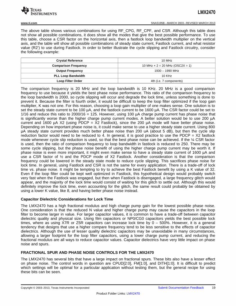
The above table shows various combinations for using RF_CPG, RF_CPF, and CSR. Although this table doesnot show all possible combinations, it does show all the modes that give the best possible performance. To usethis table, choose a CSR factor on the horizontal axis, then a fastlock loop bandwidth multiplier on the verticalaxis, and the table will show all possible combinations of steady state current, Fastlock current, and what resistorvalue (R2’) to use during Fastlock. In order to better illustrate the cycle slipping and Fastlock circuitry, considerthe following example:
Crystal Reference 10 MHz
Comparison Frequency 10 MHz × 2 = 20 MHz (OSC2X = 1)
Output Frequency 1930 – 1990 MHz
PLL Loop Bandwidth 10 KHz
Loop Filter Order 4th (i.e. 7 components)
The comparison frequency is 20 MHz and the loop bandwidth is 10 KHz. 20 MHz is a good comparisonfrequency to use because it yields the best phase noise performance. This ratio of the comparison frequency tothe loop bandwidth is 2000, so cycle slipping will occur and degrade the lock time, unless something is done toprevent it. Because the filter is fourth order, it would be difficult to keep the loop filter optimized if the loop gainmultiplier, K was not one. For this reason, choosing a loop gain multiplier of one makes sense. One solution is toset the steady state current to be 100 µA, and the fastlock current to be 1600 µA. The CSR factor could be set to1/16 and reduce this ratio to 2000/16 = 125. However, using 100 µA charge pump current has phase noise thatis significantly worse than the higher charge pump current modes. A better solution would be to use 200 µAcurrent and 1600 µA X2 (using PDCP = X2 Fastlock), since the 200 µA mode will have better phase noise.Depending on how important phase noise is, it could make sense to use a higher steady state current. Using 800µA steady state current provides much better phase noise than 200 uA (about 5 dB), but then the cycle slipreduction factor would need to be reduced to 4. In general, it is good practice to use the PDCP = X2 fastlockmode whenever cycle slip reduction is used, so that the best phase noise can be achieved. If the ¼ CSR factoris used, then the ratio of comparison frequency to loop bandwidth in fastlock is reduced to 250. There may besome cycle slipping, but the phase noise benefit of using the higher charge pump current may be worth it. Ifphase noise is even more important, it might even make sense to have a steady state current of 1600 µA anduse a CSR factor of ½ and the PDCP mode of X2 Fastlock. Another consideration is that the comparisonfrequency could be lowered in the steady state mode to reduce cycle slipping. This sacrifices phase noise forlock time. In general, using Fastlock and CSR is not the same for every application. There is a trade-off of locktime vs. phase noise. It might be tempting to try to achieve the best Fastlock benefit by using a K value of 32.Even if the loop filter could be kept well optimized in Fastlock, this hypothetical design would probably switchvery fast when the Fastlock was engaged, but then when Fastlock is disengaged, a large frequency glitch wouldappear, and the majority of the lock time would consist of waiting for this glitch to settle out. Although this woulddefinitely improve the lock time, even accounting for the glitch, the same result could probably be obtained byusing a lower K value, like 8, and having better phase noise instead.
Capacitor Dielectric Considerations for Lock Time
The LMX2470 has a high fractional modulus and high charge pump gain for the lowest possible phase noise.One consideration is that the reduced N value and higher charge pump may cause the capacitors in the loopfilter to become larger in value. For larger capacitor values, it is common to have a trade-off between capacitordielectric quality and physical size. Using film capacitors or NP0/CG0 capacitors yields the best possible locktimes, where as using X7R or Z5R capacitors can increase lock time by 0 – 500%. However, it is a generaltendency that designs that use a higher compare frequency tend to be less sensitive to the effects of capacitordielectrics. Although the use of lesser quality dielectric capacitors may be unavoidable in many circumstances,allowing a larger footprint for the loop filter capacitors, using a lower charge pump current, and reducing thefractional modulus are all ways to reduce capacitor values. Capacitor dielectrics have very little impact on phasenoise and spurs.
FRACTIONAL SPUR AND PHASE NOISE CONTROLS FOR THE LMX2470
The LMX2470 has several bits that have a large impact on fractional spurs. These bits also have a lesser effecton phase noise. The control words in question are CPUD[2:0], FM[1:0], and DITH[1:0]. It is difficult to predictwhich settings will be optimal for a particular application without testing them, but the general recipe for usingthese bits can be seen.
Copyright © 2003–2013, Texas Instruments Incorporated Submit Documentation Feedback 19
Product Folder Links: LMX2470
LMX2470
SNAS195B –MARCH 2003–REVISED MARCH 2013 www.ti.com
A good algorithm is to start with a 3rd order fractional modulator (FM=3) and dithering disabled. Then dependingon whether phase noise, fractional spurs, or sub-fractional spurs are most important, optimize the settings.Integer spurs and fractional spurs are nothing new, but sub-fractional spurs are something unique to delta-sigmaPLLs. These are spurs that occur at a fraction of the frequency of where a fractional spur would appear.
First adjust the delta-sigma modulator order. Often increasing from a 2nd to a 3rd order modulator provides alarge benefit in spur levels. Increasing from a 3rd to a 4th order modulator usually provides some benefit, but it isusually on the order of a few dB. The modulator order by far has the greatest impact on the main fractionalspurs. If the loop bandwidth is very wide, or the loop filter order is not high enough, higher order modulators willintroduce a lot of sub-fractional spurs. The second order modulator usually does not have these sub-fractionalspurs. The third order modulator will introduce them at ½ of the frequency where one would expect to see atraditional fractional spur, thus the name "sub-fractional spur". The fourth order modulator will introduce thesespurs at ½ and ¼ of where a traditional fractional spur would be. If the benefit of using a higher order modulatorseems significant enough, it may make sense to try to compensate for them using the other two test bits, ordesigning a higher order loop filter. Be aware that the impact of the modulator order on the spurs may not beconsistent across tuning voltage. When the charge pump mismatch is not so bad, the lower order modulatorsmay seem to outperform the higher order modulators, but when the worst case fractional spurs are consideredover the whole range, often the higher order modulator performs better.
Second, adjust with the CPUD[2:0] bits. Setting this bit to maximum tends to reduce the sub-fractional spurs themost, however, it may degrade phase noise by up to 1 dB.
Third, experiment with the dithering. When dithering is enabled, it may increase phase noise by up to 2 dB.However, enabling dithering may also reduce the sub-fractional spurs. Also, sometimes both the fractional spursand the sub-fractional spurs can be unpredictable with dithering disabled. This is because the delta-sigmasequence is periodic, but the starting point changes. Dithering takes these problems away. When the fractionalnumerator is 0, enabling dithering typically hurts spur performance, because it is trying to correct for spur that arenot there.
Fourth, consider experimenting with the loop filter order and comparison frequency. In general, higher order loopfilters are always better, but they require more components. Often, the best spur performance is at highercomparison frequencies as well. The reason why this is the last step is not because it has the least impact, butbecause it takes more labor to do this than to change the FM[1:0], CPUD[2:0], and DITH[1:0] bits.
Although general trends do exist, the optimal settings for test bits may depend on the comparison frequency andloop filter. Also the output frequency in important. In particular, the charge pump tuning voltage is relevant. Therecommended way to do this is to test the spur levels at the low, middle, and high range of the VCO, and use theworst case over these three frequencies as a metric for performance. Also, it is important to be aware that all therules stated above have counterexamples and exceptions. However, more often than not, these rules apply.
Programming Description
GENERAL PROGRAMMING INFORMATION
The descriptions below describe the 24-bit data registers loaded through the MICROWIRE Interface. These dataregisters are used to program the R counter, the N counter, and the internal mode control latches. The dataformat of a typical 24-bit data register is shown below. The control bits CTL [3:0] decode the register address. Onthe rising edge of LE, data stored in the shift register is loaded into one of the appropriate latches (selected byaddress bits). Data is shifted in MSB first. Note that it is best to program the N counter last, since doing soinitializes the digital lock detector and Fastlock circuitry. Note that initialize means it resets the counters, but itdoes NOT program values into these registers. Upon a cold power-up, it is necessary to program all theregisters. The exception is when 22-bit is not being used. In this case, it is not necessary to program the R7register.
MSB LSB
DATA [21:0] CTL [3:0]
23 4 3 2 1 0
20 Submit Documentation Feedback Copyright © 2003–2013, Texas Instruments Incorporated
Product Folder Links: LMX2470
LMX2470
www.ti.com SNAS195B –MARCH 2003–REVISED MARCH 2013
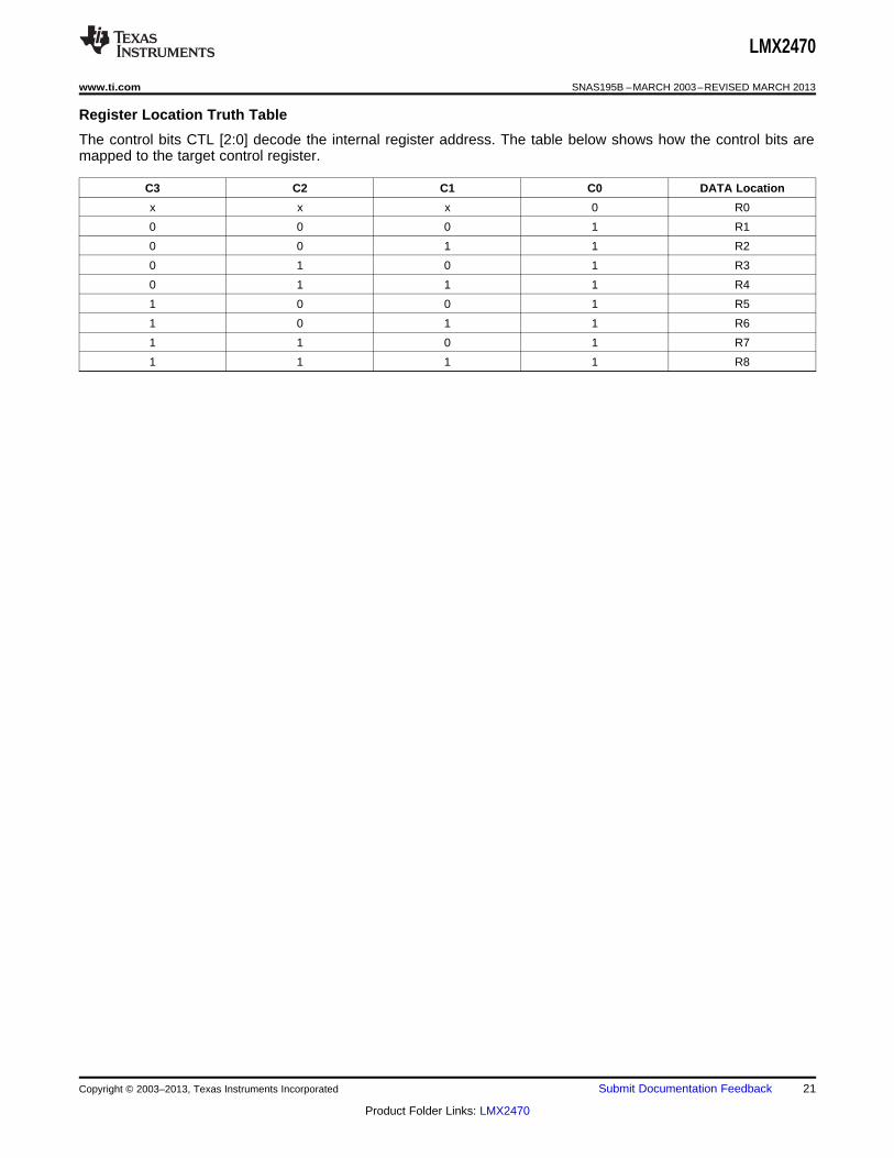
Register Location Truth Table
The control bits CTL [2:0] decode the internal register address. The table below shows how the control bits aremapped to the target control register.
C3 C2 C1 C0 DATA Location
x x x 0 R0
0 0 0 1 R1
0 0 1 1 R2
0 1 0 1 R3
0 1 1 1 R4
1 0 0 1 R5
1 0 1 1 R6
1 1 0 1 R7
1 1 1 1 R8
Copyright © 2003–2013, Texas Instruments Incorporated Submit Documentation Feedback 21
Product Folder Links: LMX2470

LMX2470
SNAS195B –MARCH 2003–REVISED MARCH 2013 www.ti.com
Control Register Content Map
Because the LMX2470 registers are complicated, they are organized into two groups, basic and advanced. The first four registers are basic registers thatcontain critical information necessary for the PLL to achieve lock. The last 5 registers are for features that optimize spur, phase noise, and lock timeperformance. The next page shows these registers.
Quick Start Register Map
Although it is highly recommended that the user eventually take advantage of all the modes of the LMX2470, the quick start register map is shown in order for the user to get the part up andrunning quickly using only those bits critical for basic functionality. The following default conditions for this programming state are a third order delta-sigma modulator in 22-bit mode with nodithering and no Fastlock.
REGISTER 23 22 21 20 19 18 17 16 15 14 13 12 11 10 9 8 7 6 5 4 3 2 1 0
DATA[19:0] (Except for the RF_N Register, which is [22:0]) C3 C2 C1 C0
R0 RF_N[10:0] RF_FN[11:0] 0
R1 RF_P 1 RF_R[5:0] RF_FD[11:0] 0 0 0 1D
R2 IF_PD IF_P IF_CP IF_N[16:0] 0 0 1 1G
R3 0 RF_CPG[3:0] IF_R[14:0] 0 1 0 1
R4 0 0 0 0 0 0 0 0 0 0 0 0 0 0 0 0 0 0 0 0 0 1 1 1
R5 0 0 0 1 0 0 0 0 0 0 0 0 0 0 0 0 0 0 0 0 1 0 0 1
R6 0 0 0 0 0 0 0 0 0 0 1 1 0 0 0 1 0 0 0 0 1 0 1 1
R7 0 0 0 0 0 0 0 0 0 0 0 0 0 0 0 0 0 0 0 0 1 1 0 1
R8 0 0 0 0 1 1 0 0 0 0 0 0 1 0 0 0 1 1 1 0 1 1 1 1
22 Submit Documentation Feedback Copyright © 2003–2013, Texas Instruments Incorporated
Product Folder Links: LMX2470
LMX2470
www.ti.com SNAS195B –MARCH 2003–REVISED MARCH 2013
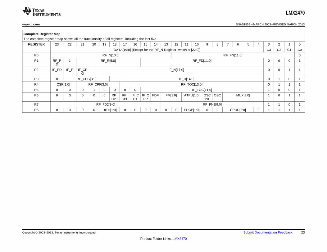
Complete Register Map
The complete register map shows all the functionality of all registers, including the last five.
REGISTER 23 22 21 20 19 18 17 16 15 14 13 12 11 10 9 8 7 6 5 4 3 2 1 0
DATA[19:0] (Except for the RF_N Register, which is [22:0]) C3 C2 C1 C0
R0 RF_N[10:0] RF_FN[11:0] 0
R1 RF_P 1 RF_R[5:0] RF_FD[11:0] 0 0 0 1D
R2 IF_PD IF_P IF_CP IF_N[17:0] 0 0 1 1G
R3 0 RF_CPG[3:0] IF_R[14:0] 0 1 0 1
R4 CSR[1:0] RF_CPF[3:0] RF_TOC[13:0] 0 1 1 1
R5 0 0 0 1 0 0 0 0 IF_TOC[11:0] 1 0 0 1
R6 0 0 0 0 0 RF_ RF_ IF_C IF_C FDM FM[1:0] ATPU[1:0] OSC OSC MUX[3:0] 1 0 1 1CPT CPP PT PP 2X
R7 RF_FD2[9:0] RF_FN2[9:0] 1 1 0 1
R8 0 0 0 0 DITH[1:0] 0 0 0 0 0 0 PDCP[1:0] 0 0 CPUD[2:0] 0 1 1 1 1
Copyright © 2003–2013, Texas Instruments Incorporated Submit Documentation Feedback 23
Product Folder Links: LMX2470
LMX2470
SNAS195B –MARCH 2003–REVISED MARCH 2013 www.ti.com
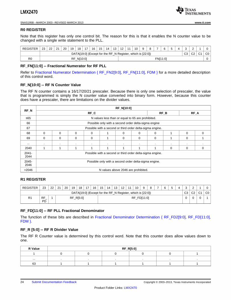
R0 REGISTER
Note that this register has only one control bit. The reason for this is that it enables the N counter value to bechanged with a single write statement to the PLL.
REGISTER 23 22 21 20 19 18 17 16 15 14 13 12 11 10 9 8 7 6 5 4 3 2 1 0
DATA[19:0] (Except for the RF_N Register, which is [22:0]) C3 C2 C1 C0
R0 RF_N[10:0] FN[11:0] 0
RF_FN[11:0] -- Fractional Numerator for RF PLL
Refer to Fractional Numerator Determination { RF_FN2[9:0], RF_FN[11:0], FDM } for a more detailed descriptionof this control word.
RF_N[10:0] -- RF N Counter Value
The RF N counter contains a 16/17/20/21 prescaler. Because there is only one selection of prescaler, the valuethat is programmed is simply the N counter value converted into binary form. However, because this counterdoes have a prescaler, there are limitations on the divider values.
RF_N[10:0]RF_N
RF_C RF_B RF_A
≤65 N values less than or equal to 65 are prohibited.
66 Possible only with a second order delta-sigma engine
67 Possible with a second or third order delta-sigma engine.
68 0 0 0 0 1 0 0 0 1 0 0
69 0 0 0 0 1 0 0 0 1 0 1
... . . . . . . . . . . .
2040 1 1 1 1 1 1 1 1 0 0 0
2041- Possible with a second or third order delta-sigma engine.2044
2045- Possible only with a second order delta-sigma engine.2046
>2046 N values above 2046 are prohibited.
R1 REGISTER
REGISTER 23 22 21 20 19 18 17 16 15 14 13 12 11 10 9 8 7 6 5 4 3 2 1 0
DATA[19:0] (Except for the RF_N Register, which is [22:0]) C3 C2 C1 C0
R1 RF_ 1 RF_R[5:0] RF_FD[11:0] 0 0 0 1PD
RF_FD[11:0] -- RF PLL Fractional Denominator
The function of these bits are described in Fractional Denominator Determination { RF_FD2[9:0], RF_FD[11:0],FDM }.
RF_R [5:0] -- RF R Divider Value
The RF R Counter value is determined by this control word. Note that this counter does allow values down toone.
R Value RF_R[5:0]
1 0 0 0 0 0 1
... . . . . . .
63 1 1 1 1 1 1
24 Submit Documentation Feedback Copyright © 2003–2013, Texas Instruments Incorporated
Product Folder Links: LMX2470
LMX2470
www.ti.com SNAS195B –MARCH 2003–REVISED MARCH 2013
RF_PD -- RF Power Down Control Bit
When this bit is set to 0, the RF PLL operates normally. When it is set to one, the RF PLL is powered down andthe RF Charge pump is set to a TRI-STATE mode. Because the EN pin and ATPU[1:0] word also controls powerdown functions, there may be some conflicts. The order of precedence is as follows. First, if the EN pin is LOW,then the PLL will be powered down. Provided this is not the case, the PLL will be powered up if the ATPU[1:0]word says to do so, regardless of the state of the RF_PD bit. After the EN pin and the ATPU[1:0] word areconsidered, then the RF_PD bit then takes control of the power down function for the RF PLL.
R2 REGISTER
REGISTER 23 22 21 20 19 18 17 16 15 14 13 12 11 10 9 8 7 6 5 4 3 2 1 0
DATA[19:0] (Except for the RF_N Register, which is [22:0]) C3 C2 C1 C0
R2 IF_P IF_P IF_C IF_N[17:0] 0 0 1 1D PG
IF_N[16:0] -- IF N Divider Value
The IF N divider is a classical dual modulus prescaler with a selectable 8/9 or 16/17 modulus. The IF_N value isdetermined by the IF_A , IF_B, and IF_P values. Note that the IF_P word can assume a value of 8 or 16. TheRF_A and RF_B counter values can be determined in accordance with the following equations.
B = N div P
A = N mod P
B≥A is required in order to have a legal N divider ratio
Here the div operator is defined as the division of two numbers with the remainder disregarded and the modoperator is defined as the remainder as a result of this division. For the purposes of programming, it turns outthat the register value is just the binary representation of the N value, with the exception that the 4th LSB is notused and must be programmed to 0 when the 8/9 prescaler is used.
IF_N Programming with the 8/9 Prescaler
IF_N[16:0]NValue IF_B IF_A
<24 N Values Below 24 are prohibited since IF_B≥3 is required.
24-55 Legal divide ratios in this range are: 24-27, 32-36, 40-45, 48-54
56 0 0 0 0 0 0 0 0 0 0 1 1 1 0 0 0 0
... . . . . . . . . . . . . . 0 . . .
6553 1 1 1 1 1 1 1 1 1 1 1 1 1 0 1 1 15
RF_N Programming with 16/17 Prescaler
IF_N[16:0]NValue IF_B IF_A
≤47 N values less than or equal to 47 are prohibited because IF_B≥3 is required.
48- Legal divide ratios in this range are: 48-51, 64-68, 80-85, 96-102239
240 0 0 0 0 0 0 0 0 0 0 1 1 1 0 0 0 0
... . . . . . . . . . . . . . . . . .
1310 1 1 1 1 1 1 1 1 1 1 1 1 1 1 1 171
Copyright © 2003–2013, Texas Instruments Incorporated Submit Documentation Feedback 25
Product Folder Links: LMX2470

LMX2470
SNAS195B –MARCH 2003–REVISED MARCH 2013 www.ti.com
IF_CPG -- IF Charge Pump Gain
This bit determines the magnitude of the IF charge pump current
IF_CPG IF Charge Pump Current (mA)
0 Low (1 mA)
1 High (4 mA)
IF_P -- IF Prescaler Value
This bit selects which prescaler will be used for the IF N counter.
IF_P IF Prescaler Value
0 8 (8/9 Prescaler)
1 16 (16/17 Prescaler)
IF_PD -- IF Power Down Bit
When this bit is set to 0, the IF PLL operates normally. When it is set to 1, the IF PLL powers down and theoutput of the IF PLL charge pump is set to a TRI-STATE mode. If the IF_CPT bit is set to 0, then the powerdown state is synchronous and will not occur until the charge pump is off. If the IF_CPT bit is set to 1, then thepower down will occur immediately regardless of the state of the IF PLL charge pump.
R3 REGISTER
REGISTER 23 22 21 20 19 18 17 16 15 14 13 12 11 10 9 8 7 6 5 4 3 2 1 0
DATA[19:0] (Except for the RF_N Register, which is [22:0]) C3 C2 C1 C0
R3 0 RF_CPG[3:0] IF_R[14:0] 0 1 0 1
IF_R[14:0] -- IF R Divider Value
For the IF R divider, the R value is determined by the IF_R[14:0] bits in the R3 register. The minimum value forIF_R is 3.
R IF_R[14:0]Value
3 0 0 0 0 0 0 0 0 0 0 0 0 0 1 1
... . . . . . . . . . . . . . . .
32767 1 1 1 1 1 1 1 1 1 1 1 1 1 1 1
RF_CPG -- RF PLL Charge Pump Gain
This is used to control the magnitude of the RF PLL charge pump in steady state operation
RF_CPG[3:0] RF Charge Pump Current (µA)
0 100
1 200
2 300
3 400
4 500
5 600
6 700
7 800
8 900
9 1000
10 1100
11 1200
12 1300
26 Submit Documentation Feedback Copyright © 2003–2013, Texas Instruments Incorporated
Product Folder Links: LMX2470

LMX2470
www.ti.com SNAS195B –MARCH 2003–REVISED MARCH 2013
RF_CPG[3:0] RF Charge Pump Current (µA)
13 1400
14 1500
15 1600
R4 REGISTER
This register controls the conditions for the RF PLL in Fastlock.
REGISTER 23 22 21 20 19 18 17 16 15 14 13 12 11 10 9 8 7 6 5 4 3 2 1 0
DATA[19:0] (Except for the RF_N Register, which is [22:0]) C3 C2 C1 C0
R4 CSR[1:0 RF_CPF[3:0] RF_TOC[13:0] 0 1 1 1]
RF_TOC -- RF Time Out Counter and Control for FLoutRF Pin
The RF_TOC[13:0] word controls the operation of the RF Fastlock circuitry as well as the function of theFLoutRF output pin. When this word is set to a value between 0 and 3, the RF Fastlock circuitry is disabled andthe FLoutRF pin operates as a general purpose CMOS TRI-STATE I/O. When RF_TOC is set to a valuebetween 4 and 16383, the RF Fastlock mode is enabled and the FLoutRF pin is utilized as the RF Fastlockoutput pin. The value programmed into the RF_TOC[13:0] word represents four times the number of phasedetector comparison cycles the RF synthesizer will spend in the Fastlock state.
RF_TOC[13:0] Fastlock Mode Fastlock Period [CP events] FLoutRF Pin Functionality
0 Disabled N/A High Impedance
1 Manual N/A Logic “0” State.Forces all fastlock conditions
2 Disabled N/A Logic “0” State
3 Disabled N/A Logic “1” State
4 Enabled 4X2 = 8 Fastlock
5 Enabled 5X2 = 10 Fastlock
… Enabled … Fastlock
16383 Enabled 16383X2=32766 Fastlock
RF_CPF -- RF PLL Fastlock Charge Pump Current
Specify the charge pump current for the Fastlock operation mode for the RF PLL. Note that the Fastlock chargepump current, steady state current, and CSR control are all interrelated. Refer to section 4.0 for more details.
RF_CPF [3:0] Fastlock Charge Pump Current (µA)
0000 100
0001 200
0010 300
0011 400
0100 500
0101 600
0110 700
0111 800
1000 900
1001 1000
1010 1100
1011 1200
1100 1300
1101 1400
1110 1500
Copyright © 2003–2013, Texas Instruments Incorporated Submit Documentation Feedback 27
Product Folder Links: LMX2470

LMX2470
SNAS195B –MARCH 2003–REVISED MARCH 2013 www.ti.com
1111 1600
RF_CSR[1:0] -- RF Cycle Slip Reduction
CSR controls the operation of the Cycle Slip Reduction Circuit. This circuit can be used to reduce the occurrenceof phase detector cycle slips. Note that the Fastlock charge pump current, steady state current, and CSR controlare all interrelated. The table below gives some rough guidelines. In the table below, fCOMP is the comparisonfrequency, and BW is the loop bandwidth of the PLL system. The rough guideline gives an idea of when it makessense to use this cycle slip reduction based on the steady-state conditions of the PLL system.
CSR[1:0] CSR State Sample Rate Reduction Factor Rough Guideline
0 Disabled 1 fCOMP < 100 × BW
1 Enabled 1/2 100 × BW < fCOMP < 200 × BW
2 Enabled 1/4 200 × BW < fCOMP < 400 × BW
3 Enabled 1/16 fCOMP > 400 × BW
R5 REGISTER
REGISTER 23 22 21 20 19 18 17 16 15 14 13 12 11 10 9 8 7 6 5 4 3 2 1 0
DATA[19:0] (Except for the RF_N Register, which is [22:0]) C3 C2 C1 C0
R5 0 0 0 0 0 0 0 0 IF_TOC[11:0] 1 0 0 1
IF_TOC[11:0] IF Timeout Counter for Fastlock
The IF_TOC word controls the operation of the IF Fastlock circuitry as well as the function of the FLoutIF outputpin. When IF_TOC is set to a value between 0 and 3, the IF Fastlock circuitry is disabled and the FLoutIF pinoperates as a general purpose CMOS TRI-STATE output. When IF_TOC is set to a value between 4 and 4095,the IF Fastlock mode is enabled and FLoutIF is utilized as the IF Fastlock output pin. The value programmed intoIF_TOC represents the number of phase comparison cycles that the IF synthesizer will spend in the Fastlockstate.
IF_TOC[11:0] Fastlock Mode Fastlock Period [Charge Pump FLoutIF Pin FunctionalityCycles]
0 Disabled N/A High Impedance
1 Manual N/A Logic “0” StateForces IF charge pump current to
4 mA
2 Disabled N/A Logic “0” State
3 Disabled N/A Logic “1” State
4 Enabled 5 Fastlock
… Enabled … Fastlock
4095 Enabled 4095 Fastlock
R6 REGISTER
REGISTER 23 22 21 20 19 18 17 16 15 14 13 12 11 10 9 8 7 6 5 4 3 2 1 0
DATA[19:0] (Except for the RF_N Register, which is [22:0]) C C C C3 2 1 0
R6 0 0 0 0 0 RF_ RF_ IF_ IF_ FDM FM[1:0] ATPU OSC OSC MUX 1 0 1 1CPT CPP CPT CPP [1:0] 2X [3:0]
28 Submit Documentation Feedback Copyright © 2003–2013, Texas Instruments Incorporated
Product Folder Links: LMX2470
LMX2470
www.ti.com SNAS195B –MARCH 2003–REVISED MARCH 2013
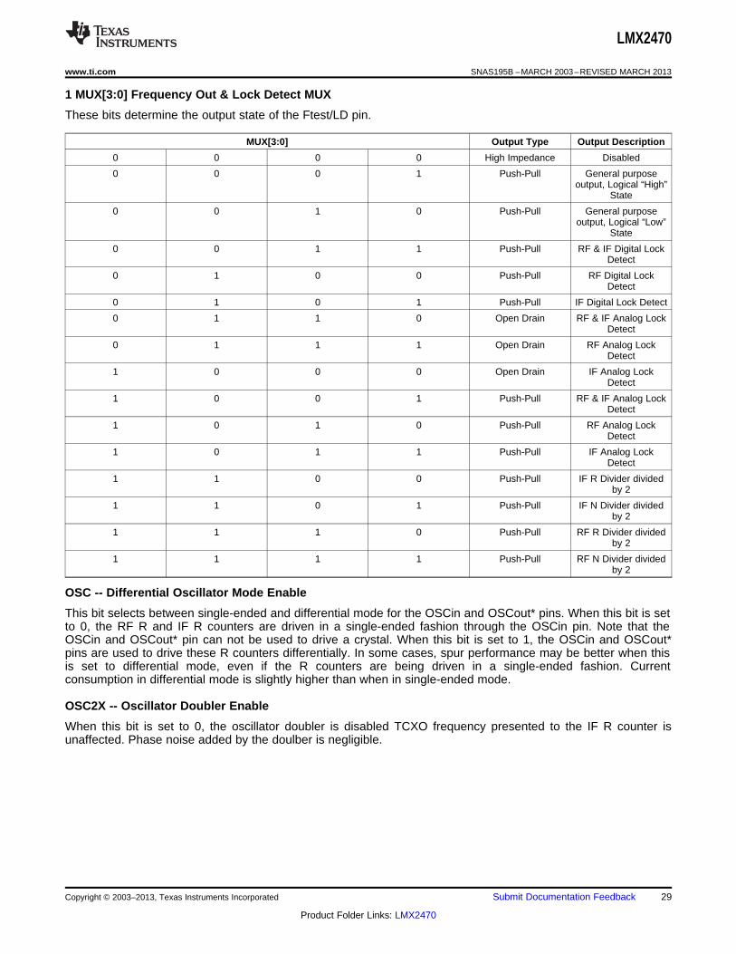
1 MUX[3:0] Frequency Out & Lock Detect MUX
These bits determine the output state of the Ftest/LD pin.
MUX[3:0] Output Type Output Description
0 0 0 0 High Impedance Disabled
0 0 0 1 Push-Pull General purposeoutput, Logical “High”
State
0 0 1 0 Push-Pull General purposeoutput, Logical “Low”
State
0 0 1 1 Push-Pull RF & IF Digital LockDetect
0 1 0 0 Push-Pull RF Digital LockDetect
0 1 0 1 Push-Pull IF Digital Lock Detect
0 1 1 0 Open Drain RF & IF Analog LockDetect
0 1 1 1 Open Drain RF Analog LockDetect
1 0 0 0 Open Drain IF Analog LockDetect
1 0 0 1 Push-Pull RF & IF Analog LockDetect
1 0 1 0 Push-Pull RF Analog LockDetect
1 0 1 1 Push-Pull IF Analog LockDetect
1 1 0 0 Push-Pull IF R Divider dividedby 2
1 1 0 1 Push-Pull IF N Divider dividedby 2
1 1 1 0 Push-Pull RF R Divider dividedby 2
1 1 1 1 Push-Pull RF N Divider dividedby 2
OSC -- Differential Oscillator Mode Enable
This bit selects between single-ended and differential mode for the OSCin and OSCout* pins. When this bit is setto 0, the RF R and IF R counters are driven in a single-ended fashion through the OSCin pin. Note that theOSCin and OSCout* pin can not be used to drive a crystal. When this bit is set to 1, the OSCin and OSCout*pins are used to drive these R counters differentially. In some cases, spur performance may be better when thisis set to differential mode, even if the R counters are being driven in a single-ended fashion. Currentconsumption in differential mode is slightly higher than when in single-ended mode.
OSC2X -- Oscillator Doubler Enable
When this bit is set to 0, the oscillator doubler is disabled TCXO frequency presented to the IF R counter isunaffected. Phase noise added by the doulber is negligible.
Copyright © 2003–2013, Texas Instruments Incorporated Submit Documentation Feedback 29
Product Folder Links: LMX2470
LMX2470
SNAS195B –MARCH 2003–REVISED MARCH 2013 www.ti.com
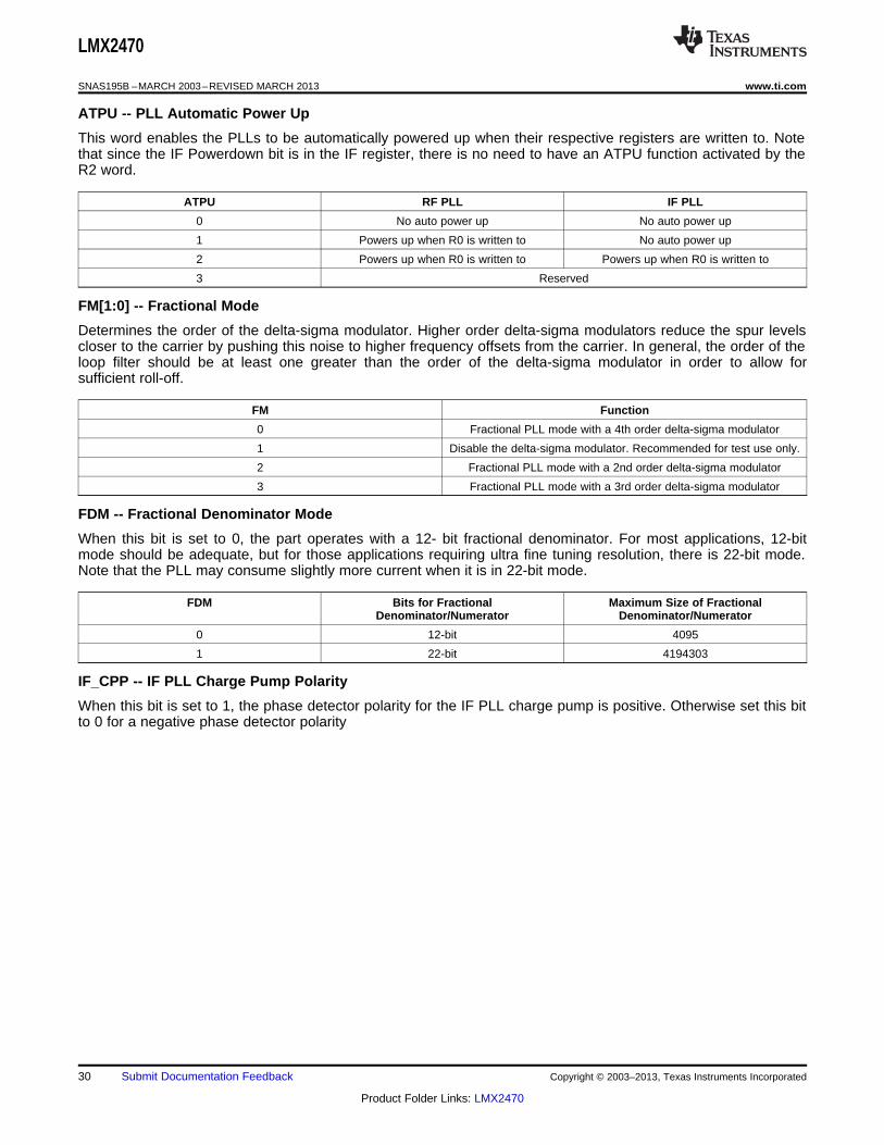
ATPU -- PLL Automatic Power Up
This word enables the PLLs to be automatically powered up when their respective registers are written to. Notethat since the IF Powerdown bit is in the IF register, there is no need to have an ATPU function activated by theR2 word.
ATPU RF PLL IF PLL
0 No auto power up No auto power up
1 Powers up when R0 is written to No auto power up
2 Powers up when R0 is written to Powers up when R0 is written to
3 Reserved
FM[1:0] -- Fractional Mode
Determines the order of the delta-sigma modulator. Higher order delta-sigma modulators reduce the spur levelscloser to the carrier by pushing this noise to higher frequency offsets from the carrier. In general, the order of theloop filter should be at least one greater than the order of the delta-sigma modulator in order to allow forsufficient roll-off.
FM Function
0 Fractional PLL mode with a 4th order delta-sigma modulator
1 Disable the delta-sigma modulator. Recommended for test use only.
2 Fractional PLL mode with a 2nd order delta-sigma modulator
3 Fractional PLL mode with a 3rd order delta-sigma modulator
FDM -- Fractional Denominator Mode
When this bit is set to 0, the part operates with a 12- bit fractional denominator. For most applications, 12-bitmode should be adequate, but for those applications requiring ultra fine tuning resolution, there is 22-bit mode.Note that the PLL may consume slightly more current when it is in 22-bit mode.
FDM Bits for Fractional Maximum Size of FractionalDenominator/Numerator Denominator/Numerator
0 12-bit 4095
1 22-bit 4194303
IF_CPP -- IF PLL Charge Pump Polarity
When this bit is set to 1, the phase detector polarity for the IF PLL charge pump is positive. Otherwise set this bitto 0 for a negative phase detector polarity
30 Submit Documentation Feedback Copyright © 2003–2013, Texas Instruments Incorporated
Product Folder Links: LMX2470
LMX2470
www.ti.com SNAS195B –MARCH 2003–REVISED MARCH 2013
IF_CPT -- IF PLL Charge Pump TRI-STATE Mode
This bit enables the user to put the charge pump in a TRI-STATE (high impedance) condition. Note that if thereis a conflict, the ATPU bit overrides this bit.
RF_CPT Charge Pump State
0 ACTIVE
1 TRI-STATE
RF_CPP -- RF PLL Charge Pump Polarity
For a positive phase detector polarity, which is normally the case, set this bit to 1. Otherwise set this bit to 0 for anegative phase detector polarity.
RF_CPT -- RF PLL Charge Pump TRI-STATE Mode
This bit enables the user to put the charge pump in a TRI-STATE (high impedance) condition. Note that if thereis a conflict, the ATPU bit overrides this bit.
RF_CPT Charge Pump State
0 Active
1 TRI-STATE
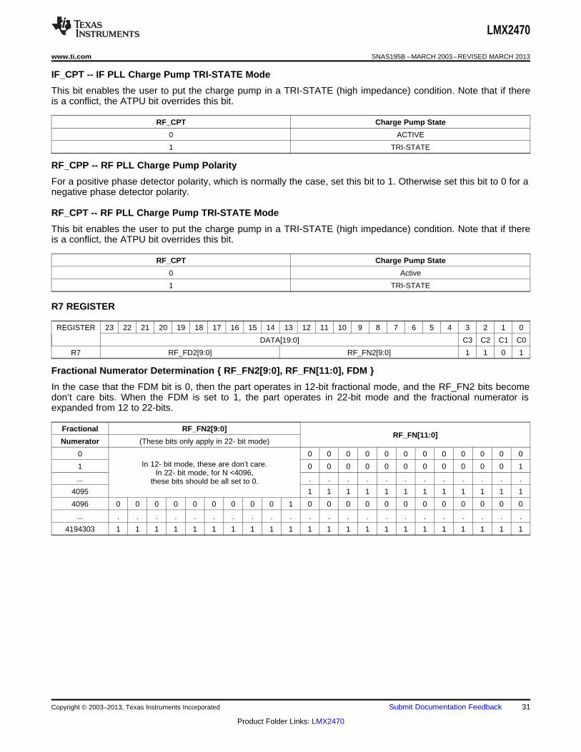
R7 REGISTER
REGISTER 23 22 21 20 19 18 17 16 15 14 13 12 11 10 9 8 7 6 5 4 3 2 1 0
DATA[19:0] C3 C2 C1 C0
R7 RF_FD2[9:0] RF_FN2[9:0] 1 1 0 1
Fractional Numerator Determination { RF_FN2[9:0], RF_FN[11:0], FDM }
In the case that the FDM bit is 0, then the part operates in 12-bit fractional mode, and the RF_FN2 bits becomedon’t care bits. When the FDM is set to 1, the part operates in 22-bit mode and the fractional numerator isexpanded from 12 to 22-bits.
Fractional RF_FN2[9:0]RF_FN[11:0]
Numerator (These bits only apply in 22- bit mode)
0 0 0 0 0 0 0 0 0 0 0 0 0In 12- bit mode, these are don’t care.1 0 0 0 0 0 0 0 0 0 0 0 1
In 22- bit mode, for N <4096,... . . . . . . . . . . . .these bits should be all set to 0.
4095 1 1 1 1 1 1 1 1 1 1 1 1
4096 0 0 0 0 0 0 0 0 0 1 0 0 0 0 0 0 0 0 0 0 0 0
... . . . . . . . . . . . . . . . . . . . . . .
4194303 1 1 1 1 1 1 1 1 1 1 1 1 1 1 1 1 1 1 1 1 1 1
Copyright © 2003–2013, Texas Instruments Incorporated Submit Documentation Feedback 31
Product Folder Links: LMX2470

LMX2470
SNAS195B –MARCH 2003–REVISED MARCH 2013 www.ti.com
Fractional Denominator Determination { RF_FD2[9:0], RF_FD[11:0], FDM }
In the case that the FDM bit is 0, then the part is operates in the 12-bit fractional mode, and the RF_FD2 bitsbecome don’t care bits. When the FDM is set to 1, the part operates in 22-bit mode and the fractionaldenominator is expanded from 12 to 22-bits.
Fractional RF_FD2[9:0] RF_FD[11:0]
Denominator (These bits only apply in 22- bit mode)
0 In 12- bit mode, these are don’t care. 0 0 0 0 0 0 0 0 0 0 0 0In 22- bit mode, for N <4096,1 0 0 0 0 0 0 0 0 0 0 0 1
these bits should be all set to 0.... . . . . . . . . . . . .
4095 1 1 1 1 1 1 1 1 1 1 1 1
4096 0 0 0 0 0 0 0 0 0 1 0 0 0 0 0 0 0 0 0 0 0 0
... . . . . . . . . . . . . . . . . . . . . . .
4194303 1 1 1 1 1 1 1 1 1 1 1 1 1 1 1 1 1 1 1 1 1 1
R8 REGISTER
23 22 21 20 19 18 17 16 15 14 13 12 11 10 9 8 7 6 5 4 3 2 1 0
DATA[19:0] C3 C2 C1 C0
R8 0 0 0 0 DITH 0 0 0 0 0 0 PDCP 0 0 CPUD 0 1 1 1 1[1:0] [1:0] [2:0]
The R8 Register controls some additional bits that may be useful in optimizing phase noise, lock time, and spurs.
CPUD[2:0] -- Charge Pump User Definition
This bit allows the user to choose from several different modes in the charge pump. The charge pump current isunaffected, but the fractional spurs and phase noise are impacted by a few dB. In some designs, particularly ifthe loop bandwidth is wide and a 4th order delta-sigma engine is used, small spurs may appear at a fraction ofwhere the first fractional spur should appear. In other designs, these sub-fractional spurs are not present. Theuser needs to use this adjustment to make these sub-fractional spurs go away, while still getting the best phasenoise possible.
CPUD Mode Name Phase Noise Sub-Fractional Spurs
0 Reserved N/A N/A
1 Reserved N/A N/A
2 Minimum Best Worst
3 Maximum Worst Best
4 Reserved N/A N/A
5 Reserved N/A N/A
6 Reserved N/A N/A
7 Nominal Medium Medium
PDCP[1:0] -- Power Drive for Charge Pump
If this bit is enabled, the Fastlock current can be doubled during Fastlock. The charge pump current in steadystate is unaffected. States 0 and 1 should never be used.
PDCP Fastlock Charge Pump Current
0 Reserved
1 Reserved
2 Double Fastlock Current
3 Disabled
32 Submit Documentation Feedback Copyright © 2003–2013, Texas Instruments Incorporated
Product Folder Links: LMX2470

LMX2470
www.ti.com SNAS195B –MARCH 2003–REVISED MARCH 2013
DITH[1:0] -- Dithering Control
Dithering is a technique used to spread out the spur energy. Enabling dithering can reduce the main fractionalspurs, but can also give rise to a family of smaller spurs. Whether dithering helps or hurts is application specific.Enabling the dithering may also increase the phase noise. In most cases where the fractional numerator is zero,dithering usually degrades performance.
Determining tends to be most beneficial in applications where there is insufficient filtering of the spurs. This oftenoccurs when the loop bandwidth is very wide or a higher order delta-sigma modulator is used. Dithering tendsnot to impact the main fractional spurs much, but has a much larger inpact on the sub-fractional spurs. If it isdecided that dithering will be used, best results will be obtained when the fractional denominator is at least 1000.
DITH Dithering Mode Used
0 Dithering Enabled
1 Reserved
2 Reserved
3 Dithering Disabled
Copyright © 2003–2013, Texas Instruments Incorporated Submit Documentation Feedback 33
Product Folder Links: LMX2470
LMX2470
SNAS195B –MARCH 2003–REVISED MARCH 2013 www.ti.com
REVISION HISTORY
Changes from Revision A (March 2013) to Revision B Page
• Changed layout of National Data Sheet to TI format .......................................................................................................... 33
34 Submit Documentation Feedback Copyright © 2003–2013, Texas Instruments Incorporated
Product Folder Links: LMX2470

PACKAGE OPTION ADDENDUM
www.ti.com 10-Dec-2020
Addendum-Page 1
PACKAGING INFORMATION
Orderable Device Status(1)
Package Type PackageDrawing
Pins PackageQty
Eco Plan(2)
Lead finish/Ball material
(6)
MSL Peak Temp(3)
Op Temp (°C) Device Marking(4/5)
Samples
LMX2470SLEX ACTIVE ULGA NPF 24 2500 RoHS & Green NIAU Level-1-260C-UNLIM -40 to 85 X2470SLE
LMX2470SLEX/NOPB ACTIVE ULGA NPF 24 2500 RoHS & Green NIAU Level-1-260C-UNLIM -40 to 85 X2470SLE
(1) The marketing status values are defined as follows:ACTIVE: Product device recommended for new designs.LIFEBUY: TI has announced that the device will be discontinued, and a lifetime-buy period is in effect.NRND: Not recommended for new designs. Device is in production to support existing customers, but TI does not recommend using this part in a new design.PREVIEW: Device has been announced but is not in production. Samples may or may not be available.OBSOLETE: TI has discontinued the production of the device.
(2) RoHS: TI defines "RoHS" to mean semiconductor products that are compliant with the current EU RoHS requirements for all 10 RoHS substances, including the requirement that RoHS substancedo not exceed 0.1% by weight in homogeneous materials. Where designed to be soldered at high temperatures, "RoHS" products are suitable for use in specified lead-free processes. TI mayreference these types of products as "Pb-Free".RoHS Exempt: TI defines "RoHS Exempt" to mean products that contain lead but are compliant with EU RoHS pursuant to a specific EU RoHS exemption.Green: TI defines "Green" to mean the content of Chlorine (Cl) and Bromine (Br) based flame retardants meet JS709B low halogen requirements of <=1000ppm threshold. Antimony trioxide basedflame retardants must also meet the <=1000ppm threshold requirement.
(3) MSL, Peak Temp. - The Moisture Sensitivity Level rating according to the JEDEC industry standard classifications, and peak solder temperature.
(4) There may be additional marking, which relates to the logo, the lot trace code information, or the environmental category on the device.
(5) Multiple Device Markings will be inside parentheses. Only one Device Marking contained in parentheses and separated by a "~" will appear on a device. If a line is indented then it is a continuationof the previous line and the two combined represent the entire Device Marking for that device.
(6) Lead finish/Ball material - Orderable Devices may have multiple material finish options. Finish options are separated by a vertical ruled line. Lead finish/Ball material values may wrap to twolines if the finish value exceeds the maximum column width.
Important Information and Disclaimer:The information provided on this page represents TI's knowledge and belief as of the date that it is provided. TI bases its knowledge and belief on informationprovided by third parties, and makes no representation or warranty as to the accuracy of such information. Efforts are underway to better integrate information from third parties. TI has taken andcontinues to take reasonable steps to provide representative and accurate information but may not have conducted destructive testing or chemical analysis on incoming materials and chemicals.TI and TI suppliers consider certain information to be proprietary, and thus CAS numbers and other limited information may not be available for release.
In no event shall TI's liability arising out of such information exceed the total purchase price of the TI part(s) at issue in this document sold by TI to Customer on an annual basis.

PACKAGE OPTION ADDENDUM
www.ti.com 10-Dec-2020
Addendum-Page 2

TAPE AND REEL INFORMATION
*All dimensions are nominal
Device PackageType
PackageDrawing
Pins SPQ ReelDiameter
(mm)
ReelWidth
W1 (mm)
A0(mm)
B0(mm)
K0(mm)
P1(mm)
W(mm)
Pin1Quadrant
LMX2470SLEX ULGA NPF 24 2500 330.0 12.4 3.8 4.8 1.3 8.0 12.0 Q1
LMX2470SLEX/NOPB ULGA NPF 24 2500 330.0 12.4 3.8 4.8 1.3 8.0 12.0 Q1
PACKAGE MATERIALS INFORMATION
www.ti.com 26-Mar-2013
Pack Materials-Page 1
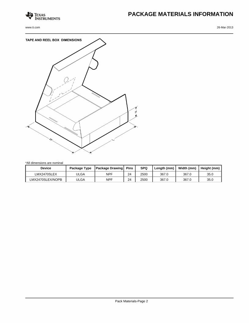
*All dimensions are nominal
Device Package Type Package Drawing Pins SPQ Length (mm) Width (mm) Height (mm)
LMX2470SLEX ULGA NPF 24 2500 367.0 367.0 35.0
LMX2470SLEX/NOPB ULGA NPF 24 2500 367.0 367.0 35.0
PACKAGE MATERIALS INFORMATION
www.ti.com 26-Mar-2013
Pack Materials-Page 2

MECHANICAL DATA
NPF0024A
www.ti.com

IMPORTANT NOTICE AND DISCLAIMER
TI PROVIDES TECHNICAL AND RELIABILITY DATA (INCLUDING DATASHEETS), DESIGN RESOURCES (INCLUDING REFERENCE DESIGNS), APPLICATION OR OTHER DESIGN ADVICE, WEB TOOLS, SAFETY INFORMATION, AND OTHER RESOURCES “AS IS” AND WITH ALL FAULTS, AND DISCLAIMS ALL WARRANTIES, EXPRESS AND IMPLIED, INCLUDING WITHOUT LIMITATION ANY IMPLIED WARRANTIES OF MERCHANTABILITY, FITNESS FOR A PARTICULAR PURPOSE OR NON-INFRINGEMENT OF THIRD PARTY INTELLECTUAL PROPERTY RIGHTS.These resources are intended for skilled developers designing with TI products. You are solely responsible for (1) selecting the appropriate TI products for your application, (2) designing, validating and testing your application, and (3) ensuring your application meets applicable standards, and any other safety, security, or other requirements. These resources are subject to change without notice. TI grants you permission to use these resources only for development of an application that uses the TI products described in the resource. Other reproduction and display of these resources is prohibited. No license is granted to any other TI intellectual property right or to any third party intellectual property right. TI disclaims responsibility for, and you will fully indemnify TI and its representatives against, any claims, damages, costs, losses, and liabilities arising out of your use of these resources.TI’s products are provided subject to TI’s Terms of Sale (www.ti.com/legal/termsofsale.html) or other applicable terms available either on ti.com or provided in conjunction with such TI products. TI’s provision of these resources does not expand or otherwise alter TI’s applicable warranties or warranty disclaimers for TI products.
Mailing Address: Texas Instruments, Post Office Box 655303, Dallas, Texas 75265Copyright © 2020, Texas Instruments Incorporated


![Multiband LTE-A/WWAN Antenna for a Tablet · MHz - 862 MHz, 2.3 GHz - 2.4 GHz, 3.4 GHz - 4.2 GHz, 4.4 GHz - 4.99 GHz [1]. LTE-A provides much high-er data rate for real-time voice](https://static.fdocuments.net/doc/165x107/5e8aca7c2ae37b1267657c33/multiband-lte-awwan-antenna-for-a-tablet-mhz-862-mhz-23-ghz-24-ghz-34.jpg)