Linearization strategies for high sensitivity ... · Linearization strategies for high sensitivity...
20
Eur. Phys. J. Appl. Phys. (2015) 72: 10601 DOI: 10.1051/epjap/2015150214 THE EUROPEAN PHYSICAL JOURNAL APPLIED PHYSICS Review Article Linearization strategies for high sensitivity magnetoresistive sensors Ana V. Silva 1,2 , Diana C. Leitao 1,2 , Jo˜ ao Valadeiro 1 , Jos´ e Amaral 1 , Paulo P. Freitas 1,3 , and Susana Cardoso 1,2, a 1 Instituto de Engenharia de Sistemas e Computadores – Microsistemas e Nanotecnologias, 1000 Lisboa, Portugal 2 Instituto Superior Tecnico, Physics Department, Universidade de Lisboa, 1049 Lisboa, Portugal 3 International Iberian Nanotechnology Laboratory, 4715 Braga, Portugal Received: 17 April 2015 / Received in final form: 28 July 2015 / Accepted: 31 August 2015 Published online: 5 October 2015 – c EDP Sciences 2015 Abstract. Ultrasensitive magnetic field sensors envisaged for applications on biomedical imaging require the detection of low-intensity and low-frequency signals. Therefore linear magnetic sensors with enhanced sensitivity low noise levels and improved field detection at low operating frequencies are necessary. Suit- able devices can be designed using magnetoresistive sensors, with room temperature operation, adjustable detected field range, CMOS compatibility and cost-effective production. The advent of spintronics set the path to the technological revolution boosted by the storage industry, in particular by the develop- ment of read heads using magnetoresistive devices. New multilayered structures were engineered to yield devices with linear output. We present a detailed study of the key factors influencing MR sensor perfor- mance (materials, geometries and layout strategies) with focus on different linearization strategies available. Furthermore strategies to improve sensor detection levels are also addressed with best reported values of ∼40 pT/ √ Hz at 30 Hz, representing a step forward the low field detection at room temperature. 1 Introduction Currently available sensing techniques include induction, fluxgate, SQUID (superconducting quantum interference device), nuclear precession, Hall-effect, magnetoresistance, magnetostrictive/piezoelectric composite, magneto- transistor, magneto-impedance, magneto-optics and MEMS (microelectromechanical systems) based magnetic sensors [1]. Their application to fields with stronger indus- trial penetration determines their development and matu- rity, thus five main technological families are dominant: SQUID sensors applied to magneto-encephalography is the prevalent technique for neuroimaging, NMR (nuclear magnetic resonance) is a powerful tool for medical diag- nose and chemical spectroscopy, resonance fluxgate sen- sors are predominant in the military industry, inductive sensors in geomagnetic research and magnetoresistive sen- sors govern the data storage industry [2]. When choosing a magnetic sensing technology different parameters need to be considered, e.g., sensitivity, linearity, field range, fre- quency bandwidth, operating temperature, dimensions. The evolution in the fabrication of thin films with well controlled thickness (as low as few ˚ A), driven by the semi-conductor industry, allowed the development of nanostructured devices. In the recent decades, the gen- eration and manipulation of spin-polarized electrons in magnetic multilayered thin-film structures gave birth to a e-mail: [email protected] spintronics, with the discovery of giant magnetoresistance by Fert et al. and Grunberg et al. in 1988 (2007 physics Nobel prize) paving the way to the digital information revolution [3]. These spintronic materials can act as extremely sensitive magnetic field sensors, because their electrical resistance can change in the presence of mag- netic fields at room temperature by factors much larger than are possible with conventional magnetic materials. Magnetoresistive (MR) sensors, with their tunable re- sponse and adjustable operation range [4], are the ideal candidates for room temperature, small footprint and cost effective applications at the pico to mili tesla (T) range (10 −12 to 10 −3 T). Field sensing can be done in an ex- tremely small, lithographically patterned area, reducing size and power consumption requirements and thus being suitable for array applications. Multiple MR sensors can be electronically addressed and multiplexed with on-board electronics. This thin film technology is compatible with standard silicon integrated circuit (IC) technology [5, 6], allowing for large scale fabrication and closed packed implementations, ideal for portable solutions. Nowadays several commercial products using MR sensors provide high performance at reasonable cost [7]. Steering angle, mechanical torque and position sensors are used in automation applications, at assembly machines and indus- trial robots [8]. Magnetometers used as digital compasses to detect the earth’s magnetic field [9] are used in the automotive industry as well as personal electronic devices. 10601-p1
-
Upload
hoangtuong -
Category
Documents
-
view
245 -
download
0
Transcript of Linearization strategies for high sensitivity ... · Linearization strategies for high sensitivity...

Eur. Phys. J. Appl. Phys. (2015) 72: 10601DOI: 10.1051/epjap/2015150214
THE EUROPEANPHYSICAL JOURNAL
APPLIED PHYSICS
Review Article
Linearization strategies for high sensitivity magnetoresistivesensors
Ana V. Silva1,2, Diana C. Leitao1,2, Joao Valadeiro1, Jose Amaral1, Paulo P. Freitas1,3, and Susana Cardoso1,2,a
1 Instituto de Engenharia de Sistemas e Computadores – Microsistemas e Nanotecnologias, 1000 Lisboa, Portugal2 Instituto Superior Tecnico, Physics Department, Universidade de Lisboa, 1049 Lisboa, Portugal3 International Iberian Nanotechnology Laboratory, 4715 Braga, Portugal
Received: 17 April 2015 / Received in final form: 28 July 2015 / Accepted: 31 August 2015Published online: 5 October 2015 – c© EDP Sciences 2015
Abstract. Ultrasensitive magnetic field sensors envisaged for applications on biomedical imaging requirethe detection of low-intensity and low-frequency signals. Therefore linear magnetic sensors with enhancedsensitivity low noise levels and improved field detection at low operating frequencies are necessary. Suit-able devices can be designed using magnetoresistive sensors, with room temperature operation, adjustabledetected field range, CMOS compatibility and cost-effective production. The advent of spintronics setthe path to the technological revolution boosted by the storage industry, in particular by the develop-ment of read heads using magnetoresistive devices. New multilayered structures were engineered to yielddevices with linear output. We present a detailed study of the key factors influencing MR sensor perfor-mance (materials, geometries and layout strategies) with focus on different linearization strategies available.Furthermore strategies to improve sensor detection levels are also addressed with best reported values of∼40 pT/
√Hz at 30 Hz, representing a step forward the low field detection at room temperature.
1 Introduction
Currently available sensing techniques include induction,fluxgate, SQUID (superconducting quantum interferencedevice), nuclear precession, Hall-effect, magnetoresistance,magnetostrictive/piezoelectric composite, magneto-transistor, magneto-impedance, magneto-optics andMEMS (microelectromechanical systems) based magneticsensors [1]. Their application to fields with stronger indus-trial penetration determines their development and matu-rity, thus five main technological families are dominant:SQUID sensors applied to magneto-encephalography isthe prevalent technique for neuroimaging, NMR (nuclearmagnetic resonance) is a powerful tool for medical diag-nose and chemical spectroscopy, resonance fluxgate sen-sors are predominant in the military industry, inductivesensors in geomagnetic research and magnetoresistive sen-sors govern the data storage industry [2]. When choosinga magnetic sensing technology different parameters needto be considered, e.g., sensitivity, linearity, field range, fre-quency bandwidth, operating temperature, dimensions.
The evolution in the fabrication of thin films withwell controlled thickness (as low as few A), driven by thesemi-conductor industry, allowed the development ofnanostructured devices. In the recent decades, the gen-eration and manipulation of spin-polarized electrons inmagnetic multilayered thin-film structures gave birth to
a e-mail: [email protected]
spintronics, with the discovery of giant magnetoresistanceby Fert et al. and Grunberg et al. in 1988 (2007 physicsNobel prize) paving the way to the digital informationrevolution [3]. These spintronic materials can act asextremely sensitive magnetic field sensors, because theirelectrical resistance can change in the presence of mag-netic fields at room temperature by factors much largerthan are possible with conventional magnetic materials.
Magnetoresistive (MR) sensors, with their tunable re-sponse and adjustable operation range [4], are the idealcandidates for room temperature, small footprint and costeffective applications at the pico to mili tesla (T) range(10−12 to 10−3 T). Field sensing can be done in an ex-tremely small, lithographically patterned area, reducingsize and power consumption requirements and thus beingsuitable for array applications. Multiple MR sensors canbe electronically addressed and multiplexed with on-boardelectronics. This thin film technology is compatible withstandard silicon integrated circuit (IC) technology [5,6],allowing for large scale fabrication and closed packedimplementations, ideal for portable solutions. Nowadaysseveral commercial products using MR sensors providehigh performance at reasonable cost [7]. Steering angle,mechanical torque and position sensors are used inautomation applications, at assembly machines and indus-trial robots [8]. Magnetometers used as digital compassesto detect the earth’s magnetic field [9] are used in theautomotive industry as well as personal electronic devices.
10601-p1
The European Physical Journal Applied Physics
Magnetoresistive sensors have been successfully appliedto industrial sensing as electrical current sensors in powersystems [10,11] or spindle high-speed measurements.Non destructive testing, either for flux leakage detectionfor packaging control [12] or metal surface cracks scan-ning [13,14], is another relevant area where MR sensorsare used. Magnetic biosensors based on MR technologyused to detect surface binding reactions of biological mole-cules labelled with magnetic particles, is an emerging fieldproviding key advantages for both research and clinicalsettings, as sensors can be arrayed and multiplexed to per-form complex protein or nucleic acid analysis in a singleassay with full scalable IC integration capability, makingit appealing for point-of-care (POC) applications alongwith lab-on-chip systems [15–21].
One of the most challenging MR detection areas isbrain activity sensing, where field signals are of very lowintensity and at low-frequency (pT range below 100 Hz),requiring sensing devices with challenging detectivity lim-its, at room temperature. Some major breakthroughs havealready been achieved, leading the way to portable neuralactivity sensing [22–24].
1.1 Magnetoresistive mechanism
A magnetoresistive device is a solid-state transducer whichdirectly converts an external magnetic field (Hext) into aresistance, given a dc bias current supply:
R = f(Hext). (1)
These devices are composed of a combination of magne-toresistive materials, whose magnetization will tend toalign with the external field and are optimized to max-imize their resistance variation [26]. The devices will havea minimum (Rmin) and a maximum (Rmax) resistanceplateau and the path from one level to other can beengineered to be a linear one, allowing them to work asmagnetic field sensors. The magnitude of the magnetore-sistance effect (MR) can be expressed as a percentage andis defined as follows:
MR(%) =Rmax − Rmin
Rmin× 100. (2)
Three main thin film magnetic sensor technologies arebased in MR: anisotropic magnetoresistance (AMR), giantmagnetoresistance (GMR) and tunnel magnetoresistance(TMR).
1.1.1 Anisotropic magnetoresistance
The AMR effect is characteristic of transition ferromag-netic materials (and their alloys), where their electricalresistance is a function of the angle between the materialmagnetization and the direction of the electrical currentflowing trough it. This phenomenon arises from spin-orbitcoupling, reflecting the interaction between the spinof the conduction electrons and the crystal lattice [27].
An increase in the resistance of the system occurs as themajority s-electrons are scattered into (minority) d-orbitalstates. The anisotropic scattering probability of thed-bands depends on the orientation of the magnetizationrelative to the flowing current, being higher when these or-bitals are parallel to the current direction and lower whenthey are perpendicular.
Typical AMR values at room temperature are ∼5% forNiFe and CoFe bulk alloys [27] and lower for patternedthin films (∼2%) [28], due to additional scattering (e.g.,grain boundaries, film interfaces). These low MR valuesare the main reason why these sensors have been graduallyreplaced by GMR and TMR devices.
1.1.2 Giant magnetoresistance
Advances in thin film deposition techniques led to thedevelopment of a new class of devices. Giant magnetore-sistance is observed in thin film multilayered structurescomposed of alternating ferromagnetic and non magneticlayers. The observed effect is a significant change in theelectrical resistance of such structures depending onwhether the magnetization of consecutive ferromagneticlayers are parallel or anti-parallel [29]. The origin of thiseffect is the (diffusive) electron spin dependent scatteringwithin the ferromagnetic layers and at their interfaces.Depending on the magnetization direction of the ferro-magnetic layers, there is an electron scattering asymmetrywhich results in different resistances for each spin depen-dent current.
The maximum resistance value is achieved when themagnetization of the ferromagnetic (FM) layers have anantiparallel configuration, while the minimum occurs for aparallel one. The existence of the GMR effect is indepen-dent of the current direction through the multilayer. Twocurrent modes are possible: current-in-plane (CIP) andcurrent-perpendicular-to-plane (CPP). The largest MRvalues are observed in CPP mode, because all conductionelectrons must pass through all layers and all spin-filterinterfaces of the structure. The highest GMR values re-ported are up to ∼65% at room temperature in CPP-GMRmultilayers [30]. However, because the active length ofthese structures is the multilayer thickness, usually muchsmaller than the typical device lateral dimensions, thesestructures exhibit very small resistances that would re-quire either sub-micron fabrication or extremely sensitiveelectrical measurements and thus are not normally usedas sensing devices.
In the beginning of the 90s, Grunberg devised a sens-ing system scheme based on the essential structure for theGMR effect (two ferromagnetic layers, separated by a nonmagnetic metallic layer, FM1/metallic spacer/FM2) [31]being readily followed by IBM’s introduction of the spinvalve (SV) system [32]. In the SV one of the FM electrodesis used as a reference direction while the other FM is freeto rotate, allowing the controlled presence of two, paralleland anti-parallel magnetization configurations [33]. Thethickness of the non-magnetic spacer is tuned in order toachieve high magnetoresistance while maintaining a small
10601-p2

A.V. Silva et al.: Linearization strategies for high sensitivity MR sensors
coupling between the two FM layers. State of the art spec-ular SVs reach MR values of the order of ∼20%. In thiscase the introduction of a small oxide layer next to theFMs induces specular reflection at the interface increas-ing electron scattering [34].
1.1.3 Tunnel magnetoresistance
Before the discovery of the GMR effect, it was alreadyknown that the electrical resistance of magnetic tunneljunctions (MTJ) depends on the relative orientation of itsferromagnetic layers, similarly to GMR [35]. This effect iscalled tunnel magnetoresistance (TMR) and has a differ-ent physical origin of the GMR effect. It occurs in multi-layered structures in which the electrons tunnel across athin (5–20 A) insulating barrier (I) sandwiched betweentwo ferromagnetic layers in a FM1/I/FM2 like structure.In these structures the electric current flows perpendicularto the layers plane (CPP configuration). The TMR effectis a result of the (non-diffusive) spin dependent tunnelingprobability. Upon applying a voltage, the electrons at theFermi level of FM1, tunnel into free equivalent spin statesat the Fermi level of FM2 and vice-versa. In ferromagneticmaterials there is an imbalance at the density of states ofthe spin up and spin down electrons near the Fermi level,which orientates the magnetization of the layer to a cer-tain direction. As a consequence, the tunneling of electronsis different according to their spins [36]. The conductanceacross the insulating barrier is dependent on the voltage atits surfaces (bias voltage) and on the ferromagnets mag-netization configuration, with the largest resistance valueachieved when the FM layers have an antiparallel orien-tation, while the lowest value occurs for the parallel con-figuration.
Overall, TMR yields a resistance variation one-twoorders of magnitude higher than GMR technology, andthus is steadily replacing the other MR technologies inmost applications. Initially, amorphous aluminum oxide(AlOx) tunnel barriers exhibited TMR values as high as∼70% at room temperature [37]. Major improvementswere achieved upon the inclusion of crystalline MgO bar-riers and textured MTJ stacks. TMR values up to ∼600%were reported at room temperature for simple CoFeB/MgO/CoFeB structures [38], and optimum values decreaseto ∼250% for complex engineered stacks developed for de-vice applications [9,39–42]. The reported high TMR val-ues are a consequence of coherent spin polarized tunneling.In fact, the physics of spin filtering has been extensivelyaddressed for single crystalline MTJs, where the electronwave functions and its attenuation rates are symmetrydependent, hence playing a major role in setting the tun-neling probability [43–45]. As stated by Tiusan et al. thispicture can also be extended to sputtered MTJ stacks [45].
Driven by the magnetic recording industry, many othersensing applications have benefited from its technologicaldevelopments. Figure 1 summarizes the technological evo-lution for this field. A wide range of other applications forMR sensors exists, that has been breached by AMR andSV based sensors, but where MTJ based sensors appear
Fig. 1. Magnetic recording technology evolution. From refer-ence [25], c©IOP Publishing. Reproduced by permission of IOPPublishing. All rights reserved.
Fig. 2. Key properties of MR technologies (for devices withµm2 dimensions). Adapted from reference [46], in press.
when their specifications surpass those of AMR or GMR.These include various types of field sensors (from nT to1 T fields) used in several electronic and industrial ap-plications [10] along with biosensing systems [15], whosespecific requirements will define which of the technologiesto use. Key properties such as operational linear range,thermal stability, materials cost, thermal treatments re-quired or electrical robustness against electrostatic dis-charge need to be evaluated together while selecting thebest type of MR technology for a particular application(Fig. 2).
1.2 Typical sensor structure
From a merely structural point of view, MTJs are verysimilar to SVs, both consisting of two ferromagnetic elec-trodes separated by a non-magnetic spacer (metallic forSVs and insulator in MTJs case). As device applicationsrequire a stable fixed reference electrode, several strate-gies can be considered: one can either resort to FM lay-ers with different coercivities (using different materialsand/or different thicknesses) or, as first introduced by
10601-p3
The European Physical Journal Applied Physics
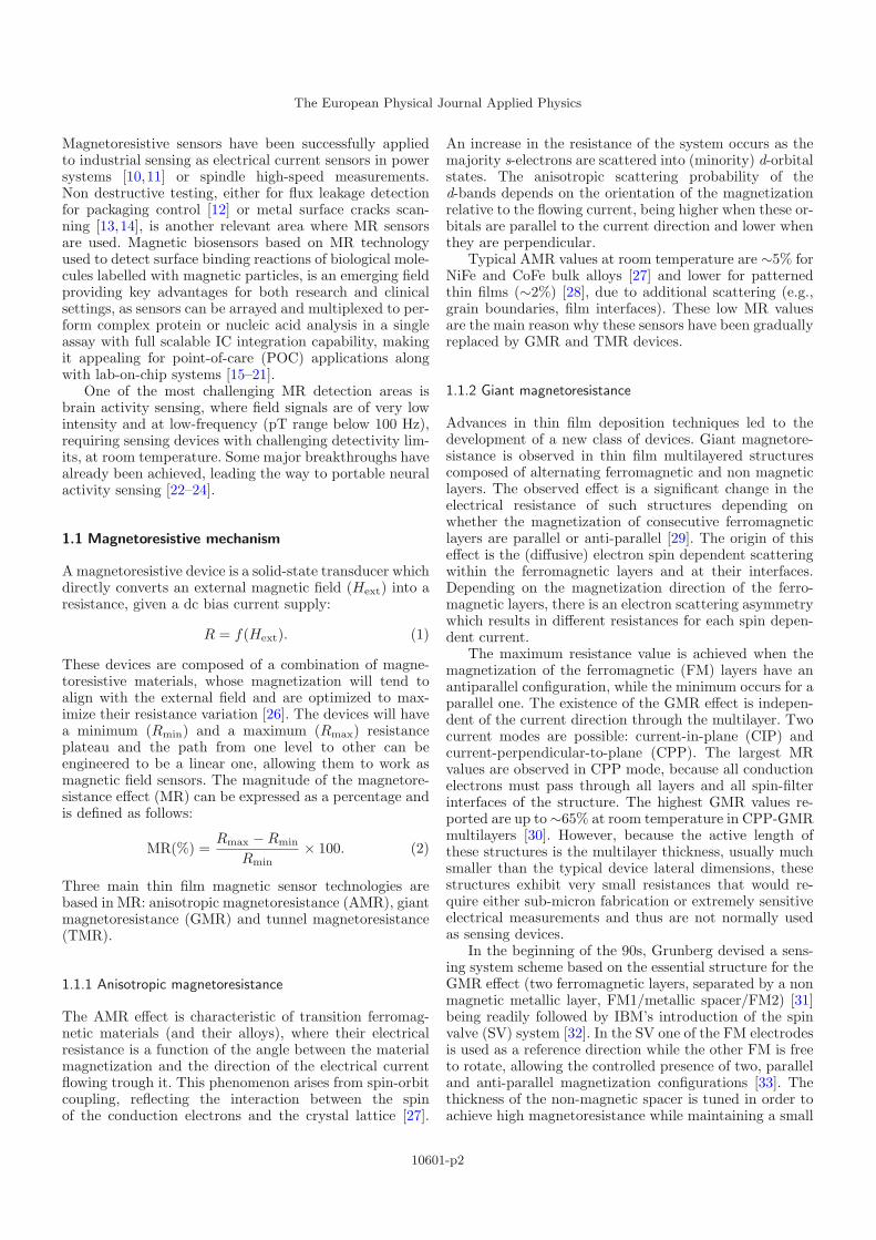
Fig. 3. Typical device structure. Arrows refer to magnetizationorientation of layers at low fields. Sensing layer dimensions:thickness (t), lateral dimensions: width (w) and height (h).
IBM [33], one can deposit an antiferromagnetic (AFM)layer adjacent to one of the FM layers, fixing its magneti-zation direction trough exchange bias coupling at the in-terface. This creates a reference direction, while the otherFM layer is free to rotate in response to a low exter-nal field, acting as a sensing electrode. Commonly usedantiferromagnetic materials include FeMn [47], NiO [48],MnIr [28] and PtMn [49]. The magnetization direction ofthis fixed layer can only be reversed at fields above theexchange bias field (μ0Hexch), which can be as high as85 mT (Hexch = 850 Oe) [50], but typically is ∼30–40 mT.The strength of the reference direction can be further en-hanced by replacing the single fixed layer by a syntheticanti-ferromagnetic (SAF) structure, which is composed oftwo ferromagnets separated by a thin spacer layer (mostcommon Ru, thinner than 1 nm), with thickness tunedto have anti-ferromagnetic coupling, as described by theRKKY theory [51]. One of the ferromagnetic layers is ex-change biased by an AFM. As a consequence, pinningfields in the order of several hundreds of kOe are ob-tained [52]. SAF structures have a null net magnetizationat low fields, being also advantageous for patterned struc-tures leading to a reduced magnetostatic coupling betweenreference and sensing layers [53]. These types of structurealso improve thermal stability and lead to a lower distri-bution of blocking temperatures [54]. Figure 3 illustratesa typical structure of such devices, comprised of /seed lay-ers/AFM/pinned FM/Ru spacer/reference FM/spacer/sensing FM/cap layers. The bottom films genericallyrepresent the underlayers commonly used to enhance elec-trical properties (e.g., CuN, Ta as buffer layers) or to pro-mote the correct crystallinity (e.g., Ta, Ru, NiFeCr as seedlayers).
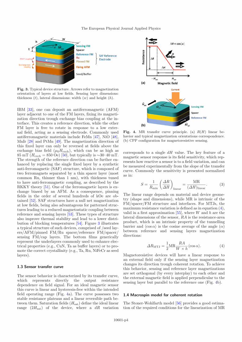
1.3 Sensor transfer curve
The sensor behavior is characterized by its transfer curve,which represents directly the output resistancedependence on field signal. For an ideal magnetic sensorthis curve is linear and hysteresis-free within the intendedfield operating range (Fig. 4a). The curve possesses twostable resistance plateaus and a linear reversible path be-tween them. Saturation fields (Hsat) define the ideal linearrange (2Hsat) of the device, where a dR variation
(a)
(b)
Fig. 4. MR transfer curve principle. (a) R(H) linear be-havior and typical magnetization orientations correspondence.(b) CPP configuration for magnetoresistive sensing.
corresponds to a single dH value. The key feature of amagnetic sensor response is its field sensitivity, which rep-resents how reactive a sensor is to a field variation, and canbe measured experimentally from the slope of the transfercurve. Commonly the sensitivity is presented normalizedas in:
S =1
Rmin
(ΔR
ΔH
)linear
=MR
(ΔH)linear. (3)
The linear range depends on material and device geome-try (shape and dimensions), while MR is intrinsic of theFM/spacer/FM structure and interfaces. For MTJs, themaximum resistance variation is defined as in equation (4),valid in a first approximation [55], where W and h are thelateral dimensions of the sensor, RA is the resistance-areaproduct, which is an intrinsic property of the tunnellingbarrier and 〈cos α〉 is the cosine average of the angle (α)between reference and sensing layers magnetizationdirections:
ΔRMTJ =12MR
RA
W × h〈cos α〉. (4)
Magnetoresistive devices will have a linear response toan external field only if the sensing layer magnetizationchanges its direction trough coherent rotation. To achievethis behavior, sensing and reference layer magnetizationsare set orthogonal (by every interplay) to each other andthe external magnetic field is applied perpendicular to thesensing layer but parallel to the reference one (Fig. 4b).
1.4 Macrospin model for coherent rotation
The Stoner-Wohlfarth model [56] provides a good estima-tion of the required conditions for the linearization of MR
10601-p4

A.V. Silva et al.: Linearization strategies for high sensitivity MR sensors
sensors with micrometric dimensions, when layers can beconsidered to have a magnetic single-domain like behaviorand edge effects can be neglected. Under these assump-tions the magnetization of a single ferromagnetic layer(M) is described as a single collective vector, whose mag-nitude (saturation magnetization – Ms) remains constantand orientation may vary in space and time, being definedby the system energy minima. The total energy associatedwith the sensing layer has two types of contributions:
Esen = Eapp + Ek,
where Eapp is the energy term associated with all magneticfields sources external to the ferromagnetic layer, definedby unit of magnetic material volume (V sen) as:
Eapp
V sen= −μ0Happ × M sen,
and where Ek represents the internal anisotropy energyterms. This term has several sources, which can be dividedin two families, one that represents all sources intrinsic tothe deposition of the ferromagnetic material, namely ofmagneto-crystalline and magnetostrictive natures and an-other family of magnetostatic nature, that represents theanisotropy created by the self-demagnetizing field of theferromagnetic layer. In this work for the intrinsicanisotropy term is only considered the uniaxial anisotropyinduced by an applied magnetic field during deposition,defined as:
Euk
V sen= −Ku sin2 φ,
where Ku is the uniaxial anisotropy constant and φ isthe angle between the ferromagnetic layer magnetizationdirection and its deposition induced easy axis (e.a.), cor-responding to a field of strength Hk = 2Ku
μ0Ms.
The self-demagnetizing term depends on shape aniso-tropy. For most geometries the exact self-demagnetiz-ing field can only be calculated numerically. For thin filmsferromagnets of micrometric lateral dimensions wheret <<< h < W , the demagnetizing field can be maximizedby:
−NhM sens cos ϕ,
where Nh is the principal component of the demagnetizingtensor N [57] along the axis parallel to h and ϕ is the anglebetween the magnetization and that axis. The energy termassociated with this field is given by:
Esenself−demag
V sen=
μ0
2Nh(M sen
s )2 cos2 ϕ.
To understand the conditions required for a MR deviceto have a linear behavior, one can consider the energybalance of the sensing layer composing the following struc-ture: reference layer/spacer/sensing layer, where the sys-tem is considered to be under the influence of an externalfield low enough for the reference layer to have its magne-tization fixed. In this situation one can consider in addi-tion to Ek terms three applied field contributions: (i) theapplied external field (Hext), (ii) the Neel coupling field
Fig. 5. Scheme of studied structure configuration. (a) Ref-erence and sensing layers with parallel induced uniaxial easyaxes. (b) Reference and sensing layers with perpendicularinduced uniaxial easy axes.
(HN ) (induced by correlated interface roughness at thespacer interfaces with the ferromagnets) and (iii) the fieldcreated at the sensing layer by the demagnetizing field ofthe reference (Href
d ).Upon material deposition, two different configurations
of sensing and reference layers can be considered (Fig. 5)one where their uniaxial induced anisotropy axes are par-allel (parallel anisotropies) and one where they are per-pendicular (crossed anisotropies). The MR device isalways aligned such that the external field to be sensedis parallel to the e.a. of the reference layer.
In the first configuration (Fig. 5a), the energy of thesensing layer (expressed relative to θ, the angle betweenthe sensing layer magnetization and external field) is givenby equation (5):
Esen
V sen= μ0M
sens
[sin2 θ
2(Hk − NhM sen
s ) +NhM sen
s
2
− cos θ(Hext − Href
d + HN
) ]. (5)
For a given range of Hext the minimization of equation (5)yields a minimum corresponding to θ = π, as long asHext is negative enough for [Hext − Href
d + HN < −|Hk
−NhM sens |] and similarly a minimum corresponding to θ =
0 is always present, as long as [Hext −Hrefd +HN > |Hk −
NhM sens |].
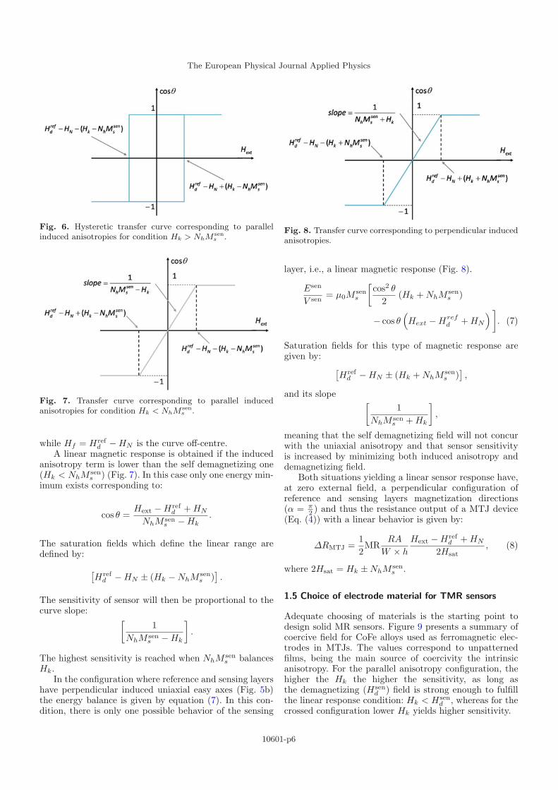
When[Hext − Href
d + HN < |Hk − NhM sens |] (moder-
ate fields) two distinct situations can occur. When theinduced anisotropy term is higher than the self demag-netizing one (Hk > NhM sen
s ) a hysteretic curve is present(Fig. 6), corresponding to two possible minima (cos θ = 1and cos θ = −1). The point where cos θ = 0 is denomi-nated coercive field (Hc) and is defined by:
Hc = Hk − NhM sens , (6)
10601-p5
The European Physical Journal Applied Physics
Fig. 6. Hysteretic transfer curve corresponding to parallelinduced anisotropies for condition Hk > NhM
sens .
Fig. 7. Transfer curve corresponding to parallel inducedanisotropies for condition Hk < NhM
sens .
while Hf = Hrefd − HN is the curve off-centre.
A linear magnetic response is obtained if the inducedanisotropy term is lower than the self demagnetizing one(Hk < NhM sen
s ) (Fig. 7). In this case only one energy min-imum exists corresponding to:
cos θ =Hext − Href
d + HN
NhM sens − Hk
.
The saturation fields which define the linear range aredefined by:
[Href
d − HN ± (Hk − NhM sens )
].
The sensitivity of sensor will then be proportional to thecurve slope: [
1NhM sen
s − Hk
].
The highest sensitivity is reached when NhM sens balances
Hk.In the configuration where reference and sensing layers
have perpendicular induced uniaxial easy axes (Fig. 5b)the energy balance is given by equation (7). In this con-dition, there is only one possible behavior of the sensing
Fig. 8. Transfer curve corresponding to perpendicular inducedanisotropies.
layer, i.e., a linear magnetic response (Fig. 8).
Esen
V sen= μ0M
sens
[cos2 θ
2(Hk + NhM sen
s )
− cos θ(Hext − Href
d + HN
) ]. (7)
Saturation fields for this type of magnetic response aregiven by:
[Href
d − HN ± (Hk + NhM sens )
],
and its slope [1
NhM sens + Hk
],
meaning that the self demagnetizing field will not concurwith the uniaxial anisotropy and that sensor sensitivityis increased by minimizing both induced anisotropy anddemagnetizing field.
Both situations yielding a linear sensor response have,at zero external field, a perpendicular configuration ofreference and sensing layers magnetization directions(α = π
2 ) and thus the resistance output of a MTJ device(Eq. (4)) with a linear behavior is given by:
ΔRMTJ =12MR
RA
W × h
Hext − Hrefd + HN
2Hsat, (8)
where 2Hsat = Hk ± NhM sens .
1.5 Choice of electrode material for TMR sensors
Adequate choosing of materials is the starting point todesign solid MR sensors. Figure 9 presents a summary ofcoercive field for CoFe alloys used as ferromagnetic elec-trodes in MTJs. The values correspond to unpatternedfilms, being the main source of coercivity the intrinsicanisotropy. For the parallel anisotropy configuration, thehigher the Hk the higher the sensitivity, as long asthe demagnetizing (Hsen
d ) field is strong enough to fulfillthe linear response condition: Hk < Hsen
d , whereas for thecrossed configuration lower Hk yields higher sensitivity.
10601-p6
A.V. Silva et al.: Linearization strategies for high sensitivity MR sensors
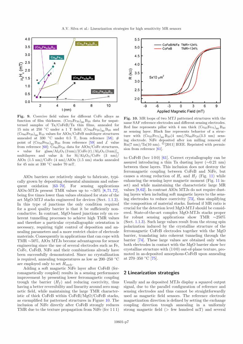
Fig. 9. Coercive field values for different CoFe alloys asfunction of film thickness. (Co70Fe30)80 B20 data for unpat-terned samples of Ta/CoFeB/Ta thin films, annealed for15 min at 250 ◦C under a 1 T field; (Co80Fe20)80 B20 and(Co80Fe20)90 B10 values for AlOx/CoFeB multilayer structuresannealed at 330 ◦C under 0.5 T, from reference [58]; #point of (Co50Fe50)80 B20 from reference [59] and £ valuefrom reference [60]; Co80Fe20 data for AlOx/CoFe structures,∗ value for glass/Al2O3 (3 nm)/[CoFe (t) /Al2O3 (3 nm)]nmultilayers and value & for Si/Al2O3/CoFe (3 nm)/AlOx (1.5 nm)/CoFe (4 nm)/AlOx (1.5 nm) stacks annealedfor 45 min at 330 ◦C under 70 mT.
AlOx barriers are relatively simple to fabricate, typi-cally grown by depositing elemental aluminum and subse-quent oxidation [63–70]. For sensing applicationsAlOx-MTJs present TMR values up to ∼50% [8,71,72],being five times lower than values obtained for state of theart MgO-MTJ stacks engineered for devices (Sect. 1.1.3).In this type of junctions the only condition requiredfor a good quality barrier is that it be sufficiently non-conductive. In contrast, MgO-based junctions rely on co-herent tunnelling processes to achieve high TMR valuesand therefore a particular crystallographic orientation isnecessary, requiring tight control of deposition and an-nealing parameters and a more restrict choice of electrodematerials. Consequently in applications that can cope withTMR ∼50%, AlOx MTJs become advantageous for sensorengineering since the use of several electrodes such as Fe,CoFe, CoFeB, NiFe and their combinations already havebeen successfully demonstrated. Since no crystallizationis required, annealing temperatures as low as 200–250 ◦Care employed only to set Hexch.
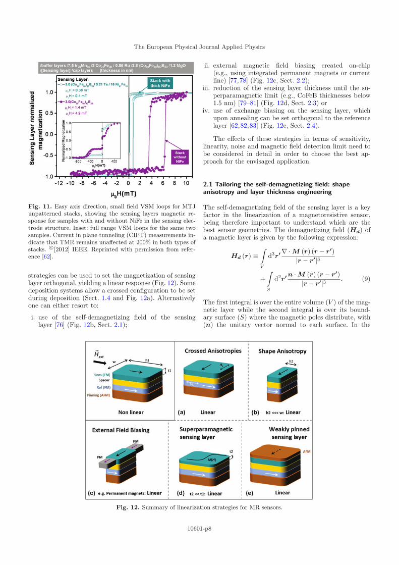
Adding a soft magnetic NiFe layer after CoFeB (fer-romagnetically coupled) results in a sensing performanceimprovement by presenting lower ferromagnetic couplingtrough the barrier (Hf ) and reducing coercivity, thushaving a better reversibility and linearity around zero mag-netic field, while maintaining the large TMR character-istic of thick CoFeB within CoFeB/MgO/CoFeB stacks,as exemplified for patterned structures in Figure 10. Theinclusion of NiFe directly after CoFeB strongly reducesTMR due to the texture propagation from NiFe (fcc 1 1 1)
Fig. 10. MR loops of two MTJ patterned structures with thesame SAF reference electrodes and different sensing electrodes.Red line represents pillar with 4 nm thick (Co25Fe75)80 B20
as sensing layer. Black line represents behavior of a struc-ture with (Co25Fe75)80 B20(4 nm)/Ni80Fe20(3.3 nm) sens-ing electrode. NiFe deposited after ion milling removal ofRu(7 nm)/Ta(10 nm). c©[2011] IEEE. Reprinted with permis-sion from reference [61].
to CoFeB (bcc 1 0 0) [61]. Correct crystallography can beassured introducing a thin Ta dusting layer (∼0.21 nm)between these layers. This inclusion does not destroy theferromagnetic coupling between CoFeB and NiFe, butcauses a strong reduction of Hc and Hf (Fig. 11) whileenhancing the sensing layer magnetic moment (Fig. 11 in-set) and while maintaining the characteristic large MRvalues [9,62]. In contrast AlOx MTJs do not require dust-ing layers when including soft magnetic layers to the sens-ing electrodes to reduce coercivity [73], thus simplifyingthe composition of material stacks. Instead if MR ratio iscrucial for the detection level MgO-MTJ should be consid-ered. State-of-the-art complex MgO-MTJs stacks properfor robust sensing applications show TMR ∼250%(Sect. 1.1.3). Such large values result from the strong spinpolarization induced by the crystalline structure of theferromagnetic CoFeB electrodes together with the MgObarrier, translating into coherent tunneling through thebarrier [74]. These large values are obtained only whenboth electrodes in contact with the MgO barrier show bcccrystalline structure with (1 0 0) out-of-plane texture, pro-moted in as-deposited amorphous-CoFeB upon annealingat 270–350 ◦C [75].
2 Linearization strategies
Usually and as deposited MTJs display a squared outputsignal, due to the parallel configuration of reference andsensing electrodes and thus cannot be straightforwardlyused as magnetic field sensors. The reference electrodemagnetization direction is defined by setting the exchangecoupling direction trough annealing in a uniformlystrong magnetic field (> few hundred mT) and several
10601-p7
The European Physical Journal Applied Physics
Fig. 11. Easy axis direction, small field VSM loops for MTJunpatterned stacks, showing the sensing layers magnetic re-sponse for samples with and without NiFe in the sensing elec-trode structure. Inset: full range VSM loops for the same twosamples. Current in plane tunneling (CIPT) measurements in-dicate that TMR remains unaffected at 200% in both types ofstacks. c©[2012] IEEE. Reprinted with permission from refer-ence [62].
strategies can be used to set the magnetization of sensinglayer orthogonal, yielding a linear response (Fig. 12). Somedeposition systems allow a crossed configuration to be setduring deposition (Sect. 1.4 and Fig. 12a). Alternativelyone can either resort to:
i. use of the self-demagnetizing field of the sensinglayer [76] (Fig. 12b, Sect. 2.1);
ii. external magnetic field biasing created on-chip(e.g., using integrated permanent magnets or currentline) [77,78] (Fig. 12c, Sect. 2.2);
iii. reduction of the sensing layer thickness until the su-perparamagnetic limit (e.g., CoFeB thicknesses below1.5 nm) [79–81] (Fig. 12d, Sect. 2.3) or
iv. use of exchange biasing on the sensing layer, whichupon annealing can be set orthogonal to the referencelayer [62,82,83] (Fig. 12e, Sect. 2.4).
The effects of these strategies in terms of sensitivity,linearity, noise and magnetic field detection limit need tobe considered in detail in order to choose the best ap-proach for the envisaged application.
2.1 Tailoring the self-demagnetizing field: shapeanisotropy and layer thickness engineering
The self-demagnetizing field of the sensing layer is a keyfactor in the linearization of a magnetoresistive sensor,being therefore important to understand which are thebest sensor geometries. The demagnetizing field (Hd) ofa magnetic layer is given by the following expression:
Hd (r) ≡∫V
d3r′ ∇ · M (r) (r − r′)|r − r′|3
+∫S
d2r′ n · M (r) (r − r′)|r − r′|3 . (9)
The first integral is over the entire volume (V ) of the mag-netic layer while the second integral is over its bound-ary surface (S) where the magnetic poles distribute, with(n) the unitary vector normal to each surface. In the
Fig. 12. Summary of linearization strategies for MR sensors.
10601-p8
A.V. Silva et al.: Linearization strategies for high sensitivity MR sensors
macrospin case: ∇ · M(r) = 0. Assuming that the layer’smagnetization is always in the sensor plane, its demagne-tizing field is also in-plane and magnetic poles are distrib-uted only along its lateral dimensions (width and height).This self-demagnetizing field, at mid-thickness, can be de-composed in components along those two directions Hd =Hh
d ex + Hwd ey, which can be expressed along the layer’s
half-width and half-height respectively as follows:⎧⎪⎪⎪⎪⎪⎪⎪⎪⎪⎨⎪⎪⎪⎪⎪⎪⎪⎪⎪⎩
Hhd ≡ −2Ms
4π
t2∫
− t2
w2∫
−w2
cos θh2√(
h2
)2+ y2 + z2
dzdy,
Hwd ≡ −2Ms
4π
t2∫
− t2
h2∫
−h2
sin θw2√
x2 +(
w2
)2 + z2dzdx.
An analytical solution for these integrals, as a functionof sensor’s dimensions was introduced by [84] assuming amacrospin behavior and W,h >> t:
⎧⎪⎪⎨⎪⎪⎩
Hhd ≡ −8Ms
4π
t√w2 + h2
w
hcos θ,
Hwd ≡ −8Ms
4π
t√w2 + h2
h
wsin θ.
(10)
Sensor designing typically takes advantage of shapeanisotropy as the sensing layer is patterned in a rectan-gular shape, with its longest dimension (width) ortho-gonal to the reference fixed direction. The higher theaspect ratio of the sensing layer dimensions (width toheight: w/h) the more dominant is Hh
d , with larger w/h
enhancing the sensor’s linear operating range and lower-ing its field sensitivity (Fig. 13). The macrospin modelbecomes advantageous for the estimation of the best de-vice dimensions afore microfabrication. Figure 14 presentsan example of such estimation, where a systematic sizeanalysis allows the determination of the aspect ratio valueat which the demagnetizing field surpasses Hk, lineariz-ing the magnetic response (w/h ≤ 50/3) from 2μ0Hsat =0.66 mT to 3.33 mT for h = 3 μm to 1 μm, respectively.
The self-demagnetizing field is also proportional to thesaturation magnetization Ms and thickness of the sensinglayer (t) (Eq. (10)). For aspect ratios above 10/1 the de-magnetizing field is maximized by − 8Ms
4πHk
th and the con-
dition of no coercivity (Eq. (6)) yields:
h < hthreshold =8Ms
4πHkt. (11)
Figure 15 presents the evolution of Ms and Hk for CoFeB((Co70Fe30)80B20) thin films as a function of layerthickness (t) from where, using the macrospin model, thethreshold height (hthreshold) at which a sensor curvechanges from square to linear, was estimated (Eq. (11)).For example, sensors using 5 nm thick (Co70Fe30)80B20
sensing layers can only have linear curves upon pattern-ing with h values below 1.2 μm, while 10 nm thick arelinear even with h = 2.8 μm heights.
Fig. 13. Transfer curves for patterned MTJ structures withdimensions w = 20 µm and varying heights. CIPT revealedaverage TMR = 200% and RA = 7.6 Ω µm2. With kind per-mission from Springer + Business Media: from reference [85].
Fig. 14. Example of macrospin simulation for sensor lineariza-tion using shape anisotropy. Same axes definition as in Sec-tion 1.4, offset fields values of µ0HN = −µ0H
refd = 0.5 mT.
2.2 External biasing
Manipulating the self-demagnetizing field can be insuf-ficient to promote a linear sensor behavior, in particularwhen the microfabrication process is not suitable for smalldimensions (h ∼ 1 μm). Moreover, if sensor area is consid-erably large (requirement of some low noiseapplications) [41], the transfer curve often presentsdiscontinuities. On the other hand, if the sensor area issignificantly small, edge roughness and other local defectsact as low anisotropy sites favoring the creation of local-ized inverted magnetization volumes which can lead tojumps in the transfer curve. Applying an external field bias(Hbias), transversal to the sensing direction can suppress
10601-p9

The European Physical Journal Applied Physics
Fig. 15. Ms and Hk experimental values for unpatterned sam-ples of Ta/CoFeB/Ta thin films, annealed for 15 min at 250 ◦Cunder a 1 T field, as a function of layer thickness and corre-sponding calculated htreshold from the macrospin model. Valuemarked with * taken from a MgO-MTJ full stack annealed for1 h at 280 ◦C under 1 T.
these effects [87–89] and promote a hysteresis-free curve.This can either be achieved with an external field or a localfield (on-chip integrated) and can be implemented with apermanent magnet (PM) or a current line loop. Externalfield creation is a bulky solution regularly used for exper-iments optimization toward a final monolithic solution.For example, on-chip permanent magnet biasing is widelyused in MR read heads. Thin film permanent magnet in-tegration allows for strict control of its dimensions andhence the magnitude of the created bias field. In contrastline loops present the disadvantage of needing electricalfeeding and could require extra powering electronics andthus being scarcely employed.
Figure 16 exemplifies MTJ based sensors with on-chipPM biasing strategy, where a reduction in Hc from 0.4 mTto 0.05 mT is visible for an isolated sensor (Fig. 16a). Mag-net efficiency depends on the gap spacing, therefore is notunexpected to see a smaller impact (still, important) inlarger sensors, or when arrays of sensors are used insteadof single elements. Figure 16b shows the impact of PM bi-asing in arrays of 82 sensors connected in series, throughreducing the (Hc) from 0.63 mT to 0.19 mT.
For current-perpendicular-to-plane configurations, thePM elements can be placed above the top electrode, af-ter top metallization deposition (Fig. 17a), avoiding anextra lithography step. This strategy was successfully val-idated in reference [78]. To ensure the best field uniformity,dimensions should be considerably larger than the sens-ing layer size. Alternatively a pair of PMs can be definedside by side the top metallization (Fig. 17b). While thislast method requires extra lithography and liftoff steps,
Fig. 16. Transfer curves for patterned MTJ structures withand without 120 nm thin film Co66Cr16Pt18 integrated per-manent magnets to create a constant field for device biasing.Unpatterned films present an average Ms ∼ 100 kA/m andµ0Hc ∼ 60 mT. (a) Single MTJ pillar behavior using a PMpair with 460 × 40 µm2 of lateral dimensions and a gap of24 µm, producing an average field at mid-sensor of 1 mT.(b) Array of in series 82 pillars with dimensions of 5 × 20 µm2
enclosed by PM with 1 × 1.2 mm2 lateral dimensions and gapof 78 µm yielding an average field at mid-array of 1.8 mT.c©[2012] IEEE. Reprinted with permission from reference [86].
it provides a far better field uniformity (created at gap)than the single PM or a loop line. The field created by thePM at the sensing layer can be calculated by equation (9),dependent on the PM magnetization, dimensions and gap.Although somehow difficult to achieve precise values forthe PM field strength at sensors with large area, Figure 18illustrates the clear impact of PM in the sensor coercivity.
10601-p10

A.V. Silva et al.: Linearization strategies for high sensitivity MR sensors
Fig. 17. Common on-chip PM biasing configuration.(a) One PM at top electrode (b) PM pair side by side withtop lead.
The linearization effect of (Hbias) can be studied by en-ergy minimization analysis, adding an extra energy term:
Esenbias
V sen= μ0M
sens Hbias sin θ,
to equations (5) and (7) of the macrospin model(Sect. 1.4). Figure 19b presents a systematic study onsensor curve coercivity with increasing external field bias,transversal to sensing direction, where above μ0Hbias =0.9 mT a linear curve is achieved. Chaves et al. havealso showed that a further increase in the bias strengthcan in particular cases lead to lower noise density at low-frequencies [90]. However this noise reduction happens atthe cost of sensitivity (Figs. 16 and 19a) and the net effectwill be an increase in the sensors detection limit. Whenthe MR sensor application targets low field detection thebest compromise is the lowest bias field possible, strongenough to linearize the MTJ and stabilize the sensing layermagnetic configuration.
2.3 Ultrathin sensing layer
On-chip biasing enlarges the final device dimensions, soif small footprint is a requirement other strategies shouldbe considered. A different approach uses a CoFeB sens-ing layer thin enough to have granular film structuresthat in the limit present a superparamagnetic (SPM) like
Fig. 18. Statistical analysis on the coercivity values (µ0Hc) ofMTJ patterned structures as a function of sensor area. Withkind permission from Springer + Business Media: from refer-ence [85].
Fig. 19. Example of macrospin simulation for sensor engi-neering using a external field bias. Same axes definition as inSection 1.4, sensor dimensions w = 50 µm and h = 50 µm,offset fields values of µ0HN = −µ0H
refd = 0.5 mT. (a) Nor-
malized sensitivity evolution of linearized curves with Hbias.(b) Coercivity of sensor response as function of Hbias. Inset:sensor curve evolution from hysteretic to linear.
behavior. These structures can be used to achieve lin-ear hysteresis-free responses, with simple designs and lowpower consumption (no external biasing element), withoutthe requirement of large aspect ratios.
In ultra-thin sensing layers at CoFeB/MgO/CoFeBstacks the perpendicular anisotropy at the sensing layer/tunnel barrier interface leads to an out-of-plane anisotropycomponent which will compete with the existent in-plane
10601-p11
The European Physical Journal Applied Physics
anisotropies [79]. The latter can result in a linear responseto in-plane magnetic fields [80,81]. Figure 20a shows theprogress of patterned MTJ transfer curves with decreas-ing sensing layer thickness. The latter presents simultane-ously both types of responses, sharp hysteretic ones withTMR values up to ∼200% (t > tcritical) and linear re-sponses with TMR values down to 40%, translating thethin CoFeB evolution from the ferromagnetic to the SPM-like regime (t ≤ tcritical). This transition is also illustratedin the inset of Figure 20a with the abrupt drop in coer-cive field at tcritical ∼ 1.45 nm which is in accordance withother reported values [79–81,92–94]. Tsai et al. estimated∼23 nm as the average lateral size of the ferromagneticparticles at the sensing layer [94] while Shen et al. ob-tained 40–120 nm [95] which for the given tcritical impliesthat the clusters have a pancake-like shape. For t ≤ tcriticala linear response is always present, independent of junc-tion area (Fig. 20b) [92]. The dramatic decrease in TMRis attributed to weakening of ferromagnetic order in thesensing layer, as the barrier conductance is proportionalto the magnetization component along the applied field,being the magnetic moment of the clusters and the layerthickness highly correlated [95].
When sensitivity is a key factor for the sensing appli-cation at hands the best thickness choice is the closer totcritical possible (t ∼ 1.5 nm), since it combines a linearhysteresis free response with the best sensitivity attain-able: 103%/mT and linear range of μ0ΔHlinear = 0.4 mT(Fig. 20a). On the other hand, when the sensor key fac-tor is a large linear range, a smaller thickness is required(t < tcritical), e.g., for t = 1.4 nm a μ0ΔHlinear = 6 mTwith 4%/mT is obtained (Fig. 20a). Zeng et al. reportswider ranges obtained with nano MTJs, with optimumvalues of μ0ΔHlinear = 60 mT and 0.2%/mT [80].
In this ultra thin CoFeB layers, even for temperaturesbelow the blocking temperature the thermal ambient en-ergy is sufficient to change the magnetization directionof the grains [94]. The resulting relaxation of magnetiza-tion orientation causes the magnetic moment of the en-tire grain to align with any applied magnetic field. Thisstrategy is therefore advantageous when both in-plane andout-of-plane field sensing is required. Teixeira et al. showed35%/mT of sensitivity and linear range of μ0ΔHlinear =0.75 mT for in-plane detection and μ0ΔHlinear = 1.6 mTand 4%/mT for out-of-plane fields, employing micrometricMTJs.
Moreover noise measurements showed negligible mag-netic noise in the sensitive region for SPM-like thicknesseswhich partially compensates the associated sensitivity lossfor lower frequency signals. However at higher frequencyones, the sensitivity decrease causes significant reductionin the signal-to-noise ratio of the devices [92], and thus dis-tinct strategies to recover the sensitivity are necessary(Sect. 3.1).
2.4 Soft exchange biasing of the sensing layer
MTJ with stack incorporated sensing layer biasing,usually consisting of a soft pinned sensing layer, have the
Fig. 20. Magneto-transport characterization for 100×100 µm2
patterned MTJ circles with varying sensing layer thickness(t). (a) Transfer curves. Inset: Corresponding coercive fieldsas function of t. (b) TMR as function of t. Reprinted withpermission from reference [91]. c©[2008], AIP Publishing LLC.
advantage of providing linear MR devices, without resort-ing to shape anisotropy or external biasing. This strategyis capable of yielding competitive sensitivity values, allow-ing a device footprint controlled only by the area of theMTJ (no additional structures), which can also be cru-cial for low detectivity applications (large area sensors;Sect. 3.2).
These multilayer stacks include two AFM films: onenext to the pinned layer and another adjacent to thesensing layer. Both AFM layers set the magnetization ofthe FM layers in a fixed direction by exchange bias(Fig. 21). However the exchange field (Hexch) of the sens-ing layer must be small as it will define the sensor satu-ration field and consequently its sensitivity. The exchange
10601-p12
A.V. Silva et al.: Linearization strategies for high sensitivity MR sensors
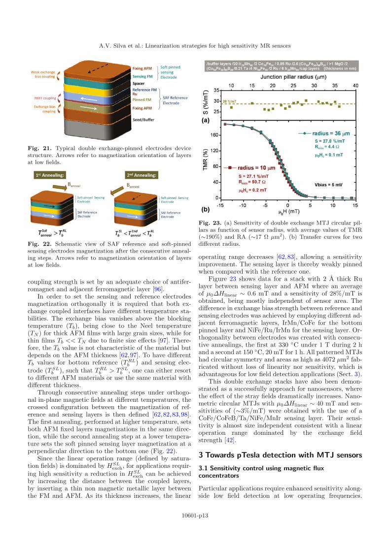
Fig. 21. Typical double exchange-pinned electrodes devicestructure. Arrows refer to magnetization orientation of layersat low fields.
Fig. 22. Schematic view of SAF reference and soft-pinnedsensing electrodes magnetization after the consecutive anneal-ing steps. Arrows refer to magnetization orientation of layersat low fields.
coupling strength is set by an adequate choice of antifer-romagnet and adjacent ferromagnetic layer [96].
In order to set the sensing and reference electrodesmagnetization orthogonally it is required that both ex-change coupled interfaces have different temperature sta-bilities. The exchange bias vanishes above the blockingtemperature (Tb), being close to the Neel temperature(TN ) for thick AFM films with large grain sizes, while forthin films Tb << TN due to finite size effects [97]. There-fore, the Tb value is not characteristic of the material butdepends on the AFM thickness [62,97]. To have differentTb values for bottom reference (TRL
b ) and sensing elec-trode (TSL
b ), such that TRLb > TSL
b , one can either resortto different AFM materials or use the same material withdifferent thickness.
Through consecutive annealing steps under orthogo-nal in-plane magnetic fields at different temperatures, thecrossed configuration between the magnetization of ref-erence and sensing layers is then defined [62,82,83,98].The first annealing, performed at higher temperature, setsboth AFM fixed layers magnetizations in the same direc-tion, while the second annealing step at a lower tempera-ture sets the soft pinned sensing layer magnetization at aperpendicular direction to the bottom one (Fig. 22).
Since the linear operation range (defined by satura-tion fields) is dominated by HSL
exch, for applications requir-ing high sensitivity a reduction in HSL
exch can be achievedby increasing the distance between the coupled layers,by inserting a thin non magnetic metallic layer betweenthe FM and AFM. As its thickness increases, the linear
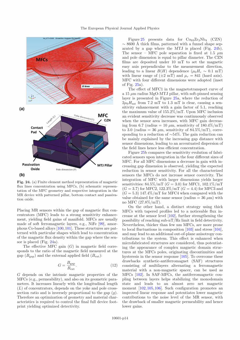
Fig. 23. (a) Sensitivity of double exchange MTJ circular pil-lars as function of sensor radius, with average values of TMR(∼190%) and RA (∼17 Ω µm2). (b) Transfer curves for twodifferent radius.
operating range decreases [62,83], allowing a sensitivityimprovement. The sensing layer is thereby weakly pinnedwhen compared with the reference one.
Figure 23 shows data for a stack with 2 A thick Rulayer between sensing layer and AFM where an averageof μ0ΔHlinear ∼ 0.6 mT and a sensitivity of 28%/mT isobtained, being mostly independent of sensor area. Thedifference in exchange bias strength between reference andsensing electrodes was achieved by employing different ad-jacent ferromagnetic layers, IrMn/CoFe for the bottompinned layer and NiFe/Ru/IrMn for the sensing layer. Or-thogonality between electrodes was created with consecu-tive annealings, the first at 330 ◦C under 1 T during 2 hand a second at 150 ◦C, 20 mT for 1 h. All patterned MTJshad circular symmetry and areas as high as 4072 μm2 fab-ricated without loss of linearity nor sensitivity, which isadvantageous for low field detection applications (Sect. 3).
This double exchange stacks have also been demon-strated as a successfully approach for nanosensors, wherethe effect of the stray fields dramatically increases. Nano-metric circular MTJs with μ0ΔHlinear ∼ 40 mT and sen-sitivities of (∼3%/mT) were obtained with the use of aCoFe/CoFeB/Ta/NiFe/MnIr sensing layer. Their sensi-tivity is almost size independent consistent with a linearoperation range dominated by the exchange fieldstrength [42].
3 Towards pTesla detection with MTJ sensors
3.1 Sensitivity control using magnetic fluxconcentrators
Particular applications require enhanced sensitivity along-side low field detection at low operating frequencies.
10601-p13
The European Physical Journal Applied Physics
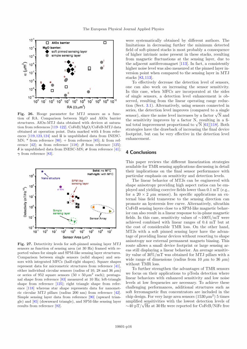
Fig. 24. (a) Finite element method representation of magneticflux lines concentration using MFCs, (b) schematic represen-tation of the MFC geometry and respective integration in theMR device with patterned pillar, bottom contact and passiva-tion oxide.
Placing MR sensors within the gap of magnetic flux con-centrators (MFC) leads to a strong sensitivity enhance-ment, yielding field gains of manifold. MFCs are usuallymade of soft ferromagnetic layers, e.g., NiFe [99], amor-phous Co-based alloys [100,101]. These structures are pat-terned with particular shapes which lead to concentrationof the magnetic flux density within the gap where the sen-sor is placed (Fig. 24a).
The effective MFC gain (G) in magnetic field corre-sponds to the ratio of the magnetic field measured at thegap (Bgap) and the external applied field (Bext):
G =Bgap
Bext. (12)
G depends on the intrinsic magnetic properties of theMFCs (e.g., permeability), and also on its geometric para-meters. It increases linearly with the longitudinal length(L) of concentrators, depends on the yoke and pole cross-section ratio and is inversely proportional to the gap (g).Therefore an optimization of geometry and material char-acteristics is required to control the final full device foot-print yielding optimized detectivity.
Figure 25 presents data for Co93Zr3Nb4 (CZN)∼ 8600 A thick films, patterned with a funnel shape sep-arated by a gap where the MTJ is placed (Fig. 24b).The sensor – MFC pole separation is fixed at 1.5 μmand pole dimension is equal to pillar diameter. The CZNfilms are deposited under 10 mT to set the magneticeasy axis perpendicular to the measurement direction,leading to a linear B(H) dependence (μ0Hc ∼ 0.1 mT)with linear range of (±2 mT) and μr = 841 (hard axis).MFC with four different dimensions were adopted (insetof Fig. 25a).
The effect of MFC1 in the magnetotransport curve ofa 15 μm radius MgO-MTJ pillar, with soft-pinned sensinglayer is presented in Figure 25a, where the reduction of2μ0Hsat from 7.2 mT to 1.3 mT is clear, causing a sen-sitivity enhancement with a gain factor of 5.1, reachingthe maximum value of 155.2%/mT. Upon MFC inclusionan evident sensitivity decrease was continuously observedwhen the sensor area increases, with MFC gain decreas-ing from 6.7 (radius = 10 μm, sensitivity of 180.4%/mT)to 3.0 (radius = 36 μm, sensitivity of 84.5%/mT), corre-sponding to a reduction of ∼54%. The gain reduction canbe mainly explained by the increasing gap distance withsensor dimensions, leading to an accentuated dispersion ofthe field lines hence less efficient concentration.
Figure 25b compares the sensitivity evolution of fabri-cated sensors upon integration in the four different sizes ofMFC. For all MFC dimensions a decrease in gain with in-creasing gap dimension is observed, yielding the expectedreduction in sensor sensitivity. For all the characterizedsensors the MFCs do not increase sensor coercivity. Theintegration of MFC with larger dimensions yields largersensitivities: 84.5%/mT (G = 3.0) for MFC1, 102.1%/mT(G = 3.7) for MFC2, 122.3%/mT (G = 4.4) for MFC3 and(G = 5.3) 147.4%/mT for MFC4 when compared with thevalue obtained for the same sensor (radius = 36 μm) withno MFC (27.8%/mT).
On the other hand, a distinct strategy using thickMFCs with tapered profiles led to a noticeable flux in-crease at the sensor level [102], further strengthening thepossibility of reaching sub-nT/Hz limit in field detectivity.Nevertheless, thicker than few nm MFCs, are more proneto local fluctuations in composition [103] and stress [104],and may lead to an additional out-of-plane anisotropy con-tributions to the system. This effect is enhanced whenmicrofabricated structures are considered, thus potentiat-ing the appearance of complex magnetic domain struc-tures at the MFCs poles, originating discontinuities andhysteresis in the sensor response [105]. To overcome thesedrawbacks synthetic-antiferromagnet (SAF) structuresconsisting of multilayers alternating a ferromagneticmaterial with a non-magnetic spacer, can be used asMFCs [102]. In SAF-MFCs, the antiferromagnetic cou-pling between layers helps stabilizing the monodomainstate and leads to an almost zero net magneticmoment [102,105,106]. Such configuration promotes animproved linear response and potentiates lower magneticcontributions to the noise level of the MR sensor, withthe drawback of smaller magnetic permeability and hencelower gains.
10601-p14

A.V. Silva et al.: Linearization strategies for high sensitivity MR sensors
Fig. 25. Double exchange MgO-MTJ sensors sensitivity en-hancement using MFCs. (a) Comparison of transfer curves for15 µm radius with and without MFCs. Inset table: dimensionsof MFCs types. (b) Comparison of sensitivity for diferent MFCsas a function of sensor area and MFC gap.
3.2 pTesla detectivity levels
The total noise of a MTJ sensor has distinct contributionsfrom thermal, shot, random telegraph and 1/f electric andmagnetic components, being the overall equation given byreference [107]. The minimum detectable field (D) of asensor corresponds to the minimum value of applied fieldwhich causes a voltage output equal to the sensor intrinsicnoise level (SV ). Therefore, to detect magnetic fields inthe pTesla range a sensor with large signal-to-noise-ratio(SNR) is required, combining high sensitivity values withlow noise levels. However, in the low frequency range thesensor SV is dominated by the 1/f component. The latterlimits the field detection level and is considered to enclosean electric and magnetic component [108]. The magneticpart arises mainly from oscillations in the magnetizationof the sensing layer, resulting from domain-wall pinningand depinning at defect sites (i.e., being maximum when
the magnetization state is changing) [108,109]. For lowfrequencies, D can be expressed by [76]:
D =1S
√αH
A × f=
ΔH
TMR
√αH
A × f(13)
being S the sensor sensitivity at the operating point, A themagnetic area of the sensor, f the operating frequency andαH the phenomenological Hooge’s parameter. Thereby,the detection level improvement implies: (i) a higher sensi-tivity steeper magnetotransport curves, (ii) largesensing area and (iii) low αH value. Figure 26 shows the re-ported αH values dependence on the resistance-area prod-uct (RA) comparing obtained data for sensors at operatingpoint for simple and soft pinned sensing layer stacks (tex-tured CoFeB/MgO/CoFeB structures including a pinnedreference layer). Overall, and for similar RA values, lowerαH values are obtained for stacks with simple sensing lay-ers when compared with soft pinned sensing layer stacks.This difference translates into lower noise levels. Thesedata are framed with reported values for AlOx (squares)whose noise was measured in the saturation state (i.e.,in the absence of local magnetization fluctuations), giv-ing a baseline for electric noise in MTJs. For additionalreference, αH values for devices optimized for memoryapplications, employing different strategies for noise levelreduction, are addressed. In all cases only saturated statesof hysteretic curves are studied. For micron sized MgOmemories, Stearret et al. reported αH = 1.3 × 10⁻⁶μm2
higher then our typical values of ∼10−8μm2 for RA ∼tens of kΩ μm2 [110]. For nanometric memories, Herranzet al. obtained a αH ∼ 6 × 10⁻¹⁰μm2 [111], increasingto αH = 3 × 10⁻⁸μm2 [112] when a soft pinned sensinglayer was used, in line with our presented results [113].Interestingly, Yu et al. showed that a double barrier ofCoFeB-MgO MTJ presents slightly lower hooge values(αH = 1.2 × 10⁻¹⁰μm2 with RA = 150 kΩ μm2) thansingle barrier MgO-MTJs, resembling two single MTJ inseries, hence providing improved signal to noise ratiounder lower bias voltage [114]. Overall, lower αH
∼ 10−10μm2 (∼40 kΩ μm2) values are achieved with sin-gle crystalline Fe/MgO/Fe MTJs [115], although for 12monolayers of MgO a similar increase of αH to 10−5μm2
was reported [116]. In the latter case, where MgO thick-ness reaches or overcomes the critical value of Fe lat-tice matching, C-doping is effective in decreasing αH to109−10−10μm2, hence decreasing the low frequency noise.This can give an alternative tool to tune MgO junctionsfor low frequency applications [116,117].
Figure 27 compares the detection levels as functionof the sensing area obtained with different sensor layouts(single isolated sensors, arrays of sensors in series, or in-cluding MFCs) and also considering distinct types of MTJstacks namely enclosing simple, SPM-like and soft-pinnedsensing layers. Although the use of a soft-pinned sensinglayer is an effective strategy to linearize sensors withoutincreasing device footprint, detectivity values two ordersof magnitude higher than those achieved using single sen-sors with simple sensing layers (∼ tens of pTesla) [85,90]
10601-p15
The European Physical Journal Applied Physics
Fig. 26. Hooge parameter for MTJ sensors as a func-tion of RA. Comparison between MgO and AlOx barrierstructures. AlOx-MTJ data obtained with devices at satura-tion from references [119–122]. CoFeB/MgO/CoFeB-MTJ dataobtained at operation point. Data marked with i from refer-ences [119,123,124] and ii is unpublished data from INESC-MN; * from reference [90]; + from reference [85]; & from ref-erence [42]; α from reference [118]; β from reference [125];δ is unpublished data from INESC-MN; σ from reference [41];γ from reference [83].
Fig. 27. Detectivity levels for soft-pinned sensing layer MTJsensors as function of sensing area (at 30 Hz) framed with re-ported values for simple and SPM-like sensing layer structures.Comparison between single sensors (solid shapes) and sen-sors with integrated MFCs (half-right shapes). Square shapesrepresent data for micrometric structures from reference [41],either individual circular sensors (radius of 10, 28 and 36 µm)or series of 952 square sensors (50 × 50µm2 each); pentago-nal shape from reference [83] measured at 10 Hz; left-triangleshape from reference [125]; right triangle shape from refer-ence [118] whereas star shape represents data for nanomet-ric circular MTJ pillars (radius 200 nm) from reference [42].Simple sensing layer data from reference [90] (upward trian-gle) and [85] (downward triangle), and SPM-like sensing layerresults from reference [92].
were systematically obtained by different authors. Thelimitations in decreasing further the minimum detectedfield of soft-pinned stacks is most probably a consequenceof higher intrinsic noise present in these stacks, resultingfrom magnetic fluctuations at the sensing layer, due tothe adjacent antiferromagnet [113]. In fact, a consistentlyhigher noise level was also measured at the pinned layer in-version point when compared to the sensing layer in MTJstacks [83,113].
To effectively decrease the detection level of sensors,one can also work on increasing the sensor sensitivity.In this case, when MFCs are incorporated at the sidesof single sensors, a detection level enhancement is ob-served, resulting from the linear operating range reduc-tion (Sect. 3.1). Alternatively, using sensors connected inseries, the detection level improves (compared to a singlesensor), since the noise level increases by a factor
√N and
the sensitivity improves by a factor N, resulting in a fi-nal total improvement proportional to
√N [61][118]. Both
strategies have the drawback of increasing the final devicefootprint, but can be very effective in the detection levelenhancement.
4 Conclusions
This paper reviews the different linearization strategiesavailable for TMR sensing applications discussing in detailtheir implications on the final sensor performance withparticular emphasis on sensitivity and detection levels.
The linear behavior of MTJs can be engineered withshape anisotropy providing high aspect ratios can be em-ployed and yielding coercive fields lower than 0.1 mT (e.g.,for a 20 × 2 μm sensor). In specific applications an ex-ternal bias field transverse to the sensing direction canpromote an hysteresis free curve. Alternatively, ultrathinCoFeB sensing layers close to a SPM-like magnetic behav-ior can also result in a linear response to in-plane magneticfields. In this case, sensitivity values of ∼100%/mT wereachieved combined with linear ranges of 0.4 mT but atthe cost of considerable TMR loss. On the other hand,MTJs with a soft pinned sensing layer have the advan-tage of providing linear devices without resorting to shapeanisotropy nor external permanent magnets biasing. Thisroute allows a small device footprint or large sensing ar-eas still displaying a linear behavior. An average sensitiv-ity value of 30%/mT was obtained for MTJ pillars with awide range of dimensions (radius from 10 μm to 36 μm)without TMR loss.
To further strengthen the advantages of TMR sensorswe focus on their applications to pTesla detection wherelinear behaviors with enhanced sensitivity and low noiselevels at low frequencies are necessary. To achieve thesechallenging performances, additional structures such assoft ferromagnetic flux concentrators are included in thechip design. For very large area sensors (1530μm2) 5 timesamplified sensitivities with the lowest detection levels of∼40 pT/
√Hz at 30Hz were reported for CoFeB/NiFe free
10601-p16

A.V. Silva et al.: Linearization strategies for high sensitivity MR sensors
layer MTJs. These results outlook MTJ sensors appli-cation to biomedical imaging at room temperature andreinforce the position and versability of magnetoresistivesensors.
The authors would like to thank R.M. Pinto for his contribu-tion in the graphical editing of the document. A.V. Silva andD.C. Leitao thank FCT for grants SFRH/BD/1719751/2010and SFRH/BPD/72359/2010. Work partially supported byprojects MAGNETRODES (EU-FP7-ICT-600730), EXCL/CTM-NAN/0441/2012 and PTDC/EEI-PRO/3219/2012.
References
1. J. Lenz, A.S. Edelstein, IEEE Sens. J. 6, 631 (2006)2. S. Tumanski, Przeglad Elektrotechniczny R. 89, 1
(2013)3. www.nobelprize.org/nobel prizes/physics/
laureates/2007/advanced-physicsprize2007.pdf
4. D.E. Heim, R.E. Fontana Jr., C. Tsang, V.S. Speriosu,B.A. Gurney, M.L. Williams, IEEE Trans. Magn. 30, 316(1994)
5. S.H. Voldman, A.J. Wallash, R.B. Wilcox Jr., Patent US5559051A, Process for manufacturing a silicon chip withan integrated magnetoresistive head mounted on a slider,1996
6. D.A. Hall, R.S. Gaster, K.A.A. Makinwa, S.X. Wang,B. Murmann, IEEE J. Solid-State Circuits 48, 1290(2013)
7. www.sensitec.com/english/technology/mr-sensor-
technology/mr sensortechnologie.html
8. M. Tondra, A. Jander, C.A. Nordman, J. Anderson,Z. Qian, D. Wang, Three-axis magnetometers using spin-dependent tunneling: reduced size and power, in Proc.SPIE 5090, Unattended Ground Sensor Technologies andApplications V, vol. 5090, edited by E.M. Carapezza(SPIE, International society for optics and photonics,Orlando, USA, 2003), p. 208
9. R. Ferreira, E. Paz, P.P. Freitas, J. Ribeiro, J. Germano,L. Sousa, IEEE Trans. Magn. 48, 4107 (2012)
10. A. Lopes, S. Cardoso, R. Ferreira, E. Paz, F.L. Deepak,J. Sanchez, D. Ramirez, S.I. Ravelo, P.P. Freitas, IEEETrans. Magn. 49, 3866 (2013)
11. Y. Ouyang, J. He, J. Hu, S.X. Wang, Sensors 12, 15520(2012)
12. D.C. Leitao, J. Borme, A. Orozco, S. Cardoso, P.P.Freitas, Giant Magnetoresistance (GMR) Sensors, vol. 6(Springer, Berlin, Heidelberg, 2013), pp. 275–299
13. A. Jander, C. Smith, R. Schneider, Magnetoresistive sen-sors for nondestructive evaluation (invited paper), inProc. SPIE 5770, Advanced Sensor Technologies for Non-destructive Evaluation and Structural Health Monitor-ing, vol. 5770, edited by N. Meyendorf, G.Y. Baaklini,B. Michel (SPIE, International society for optics and pho-tonics, San Diego, USA, 2005), p. 1
14. F.A. Cardoso, L. Rosado, R. Ferreira, E. Paz, S. Cardoso,P.M. Ramos, M. Piedade, P.P. Freitas, J. Appl. Phys.115, 17E516 (2014)
15. D.L. Graham, H.A. Ferreira, P.P. Freitas, Trends Biotech-nol. 22, 455 (2004),
16. V.C. Martins, F.A. Cardoso, J. Germano, S. Cardoso,L. Sousa, M. Piedade, P.P. Freitas, L.P. Fonseca, Biosens.Bioelectron. 24, 2690 (2009)
17. P.P. Freitas, F.A. Cardoso, V.C. Martins,S.A.M. Martins, J. Loureiro, J. Amaral, R.C. Chaves,S. Cardoso, L.P. Fonseca, A.M. Sebastiao, M. Pannetier-Lecoeur, C. Fermon, Lab on a Chip 12, 546 (2012)
18. R.S. Gaster, D.A. Hall, S.X. Wang, Lab on a Chip 11,950 (2011)
19. L. Xu, H. Yu, M.S. Akhras, S.-J. Han, S. Osterfeld, R.L.White, N. Pourmand, S.X. Wang, Biosens. Bioelectron.24, 99 (2008)
20. J. Nordling, R.L. Millen, H.A. Bullen, M.D. Porter, Anal.Chem. 80, 7930 (2008)
21. G. Li, S. Sun, R.J. Wilson, R.L. White, N. Pourmand,S.X. Wang, Sens. Actuators A: Phys. 126, 98 (2006)
22. M. Pannetier, C. Fermon, G. Le Goff, J. Simola, E. Kerr,Science 304, 1648 (2004)
23. J. Amaral, S. Cardoso, P.P. Freitas, A.M. Sebastiao,J. Appl. Phys. 109, 07B308 (2011)
24. J. Amaral, V. Pinto, T. Costa, J. Gaspar, R. Ferreira,E. Paz, S. Cardoso, P.P. Freitas, IEEE Trans. Magn. 49,3512 (2013)
25. S. Yuasa, D.D. Djayaprawira, J. Phys. D: Appl. Phys. 40,R337 (2007)
26. W. Thomson, Proc. R. Soc. Lond. 8, 546 (1857)27. T. McGuire, R. Potter, IEEE Trans. Magn. 11, 1018
(1975)28. V. Gehanno, P.P. Freitas, A. Veloso, J. Ferreira,
B. Almeida, B. Sousa, A. Kling, M.F. Da Silva, IEEETrans. Magn. 35, 4361 (1999)
29. M.N. Baibich, J.M. Broto, A. Fert, F.N. Van Dau,F. Petroff, P. Etienne, G. Creuzet, A. Friederich,J. Chazelas, Phys. Rev. Lett. 61, 2472 (1988)
30. S.S.P. Parkin, Z.G. Li, D.J. Smith, Appl. Phys. Lett. 58,2710 (1991)
31. P. Grunberg, Patent US 4949039 A, Magnetic field sen-sor with ferromagnetic thin layers having magneticallyantiparallel polarized components, 1990
32. B. Dieny, B.A. Gurney, S. Metin, S.S.P. Parkin, V.S.Speriosu, Patent US 5159513 A, Magnetoresistive sensorbased on the spin valve effect, 1991
33. B. Dieny, V.S. Speriosu, S.S.P. Parkin, B.A. Gurney,D.R. Wilhoit, D. Mauri, Phys. Rev. B 43, 1297(1991)
34. J. Hong, H. Kanai, Y. Uehara, Very large GMR of spinvalve with specularly reflective layers, in INTERMAGEurope 2002. Digest of Technical Papers, 2002, p. CA3
35. M. Julliere, Phys. Lett. A 54, 225 (1975)36. R. Meservey, P.M. Tedrow, Phys. Rep. 238, 173 (1994)37. D. Wang, C. Nordman, J.M. Daughton, Z. Qian, J. Fink,
IEEE Trans. Magn. 40, 2269 (2004)38. S. Ikeda, J. Hayakawa, Y. Ashizawa, Y.M. Lee, K. Miura,
H. Hasegawa, M. Tsunoda, F. Matsukura, H. Ohno, Appl.Phys. Lett. 93, 082508 (2008)
39. D. Watanabe, M. Oogane, S. Mizukami, Y. Ando,T. Miyazaki, Jpn J. Appl. Phys. 48, 013001 (2009)
40. F.A. Cardoso, L.S. Rosado, F. Franco, R. Ferreira,E. Paz, S.F. Cardoso, P.M. Ramos, M. Piedade, P.P.Freitas, IEEE Trans. Magn. 50, 1 (2014)
10601-p17
The European Physical Journal Applied Physics
41. J.P. Valadeiro, J. Amaral, D.C. Leitao, R. Ferreira,S. Freitas Cardoso, P.P. Freitas, IEEE Trans. Magn. 51,1 (2015)
42. D.C. Leitao, E. Paz, A.V. Silva, A. Moskaltsova,S. Knudde, F.L. Deepak, R. Ferreira, S. Cardoso, P.P.Freitas, IEEE Trans. Magn. 50, 1 (2014)
43. W.H. Butler, X.-G. Zhang, T.C. Schulthess, J.M.MacLaren, Phys. Rev. B 63, 054416 (2001)
44. S. Yuasa, T. Nagahama, A. Fukushima, Y. Suzuki,K. Ando, Nat. Mater. 3, 868 (2004)
45. C. Tiusan, F. Greullet, M. Hehn, F. Montaigne,S. Andrieu, A. Schuhl, Phys. B: Condens. Matter 19,165201 (2007)
46. S. Cardoso, S. Knudde, R.C. Chaves, F.A. Cardoso, P.P.Freitas, Magnetic Nanoparticles in Biosensing and Medi-cine (Cambridge University Press, Cambridge, UK,2015)
47. T.G.S.M. Rijks, R. Coehoorn, J.T.F. Daemen, W.J.M. deJonge, J. Appl. Phys. 76, 1092 (1994)
48. B.A. Everitt, D. Wang, J.M. Daughton, IEEE Trans.Magn. 32, 4657 (1996)
49. J.R. Childress, M.M. Schwickert, R.E. Fontana, M.K.Ho, P.M. Rice, B.A. Gurney, J. Appl. Phys. 89, 7353(2001)
50. W.J. Gallagher, S.S.P. Parkin, Y. Lu, X.P. Bian,A. Marley, K.P. Roche, R.A. Altman, S. Rishton, J. Appl.Phys. 81, 3741 (1997)
51. M.D. Stiles, Ultrathin Magnetic Structures III, editedby J. Bland, B. Heinrich (Springer, Berlin, Heidelberg,2005), pp. 99–142
52. A.V. Silva, D.C. Leitao, Z. Huo, R.J. Macedo,R. Ferreira, E. Paz, F.L. Deepak, S. Cardoso, P.P. Freitas,IEEE Trans. Magn. 49, 4405 (2013)
53. M. Rickart, A. Guedes, B. Negulescu, J. Ventura, J.B.Sousa, P. Diaz, M. MacKenzie, J.N. Chapman, P.P.Freitas, Eur. Phys. J. B 45, 207 (2005)
54. G.W. Anderson, Y. Huai, M. Pakala, J. Appl. Phys. 87,5726 (2000)
55. H. Jaffres, D. Lacour, F. Nguyen Van Dau, J. Briatico,F. Petroff, A. Vaures, Phys. Rev. B 64, 064427(2001)
56. F.J. Friedlaender, E. Kneller, S. Methfessel, D. Wagner,IEEE Trans. Magn. 27, 3469 (1991)
57. R. Engel-Herbert, T. Hesjedal, J. Appl. Phys. 97, 074504(2005)
58. S. Cardoso, C. Cavaco, R. Ferreira, L. Pereira, M. Rickart,P.P. Freitas, N. Franco, J. Gouveia, N.P. Barradas,J. Appl. Phys. 97, 10C916 (2005)
59. J. Hayakawa, S. Ikeda, Y.M. Lee, R. Sasaki, T. Meguro,F. Matsukura, H. Takahashi, H. Ohno, Jpn J. Appl. Phys.45, L1057 (2006)
60. G. Feng, S. van Dijken, J.F. Feng, J.M.D. Coey, T. Leo,D.J. Smith, J. Appl. Phys. 105, 033916 (2009)
61. S.H. Liou, X. Yin, S.E. Russek, R. Heindl, F.C.S. da Silva,J. Moreland, D.P. Pappas, L. Yuan, J. Shen, IEEE Trans.Magn. 47, 3740 (2011)
62. R. Ferreira, E. Paz, P.P. Freitas, J. Wang, S. Xue, IEEETrans. Magn. 48, 3719 (2012)
63. E.Y. Chen, R. Whig, J.M. Slaughter, D. Cronk,J. Goggin, G. Steiner, S. Tehrani, J. Appl. Phys. 87, 6061(2000)
64. X. Batlle, B.J. Hattink, A. Labarta, J. Akerman,R. Escudero, I.K. Schuller, J. Magn. Magn. Mater. 260,78 (2003)
65. J. Akerman, J.M. Slaughter, R.W. Dave, I.K. Schuller,Appl. Phys. Lett. 79, 3104 (2001)
66. Z.G. Zhang, P.P. Freitas, A.R. Ramos, N.P. Barradas,J.C. Soares, Appl. Phys. Lett. 79, 2219 (2001)
67. H. Boeve, J. De Boeck, G. Borghs, J. Appl. Phys. 89, 482(2001)
68. P.P. Freitas, S. Cardoso, R. Sousa, W. Ku, R. Ferreira,V. Chu, J.P. Conde, IEEE Trans. Magn. 36, 2796(2000)
69. S. Tehrani, B. Engel, J.M. Slaughter, E. Chen,M. DeHerrera, M. Durlam, P. Naji, R. Whig, J. Janesky,J. Calder, IEEE Trans. Magn. 36, 2752 (2000)
70. J. Akerman, M. DeHerrera, J.M. Slaughter, R. Dave, J.J.Sun, J.T. Martin, S. Tehrani, IEEE Trans. Magn. 42,2661 (2006)
71. D. Wang, J.M. Daughton, Z. Qian, M. Tondra,C. Nordman, IEEE Trans. Magn. 39, 2812(2003)
72. S.X. Wang, S.-Y. Bae, G. Li, S. Sun, R.L. White, J.T.Kemp, C.D. Webb, J. Magn. Magn. Mater. 293, 731(2005)
73. T. Zhao, K. Zhang, H.-C. Wang, Y.-H. Chen, M. Li,Patent US 7333306B2, Magnetoresistive spin valve sen-sor with tri-layer free layer, 2008
74. S.S.P. Parkin, C. Kaiser, A. Panchula, P.M. Rice,B. Hughes, M. Samant, S.H. Yang, Nat. Mater. 3, 862(2004)
75. J. Hayakawa, S. Ikeda, Y.M. Lee, R. Sasaki, T. Meguro,F. Matsukura, H. Takahashi, H. Ohno, Jpn J. Appl. Phys.44, L1267 (2005)
76. P.P. Freitas, R. Ferreira, S. Cardoso, F. Cardoso, J. Phys.:Condens. Matter 19, 165221 (2007)
77. K.B. Klaassen, X. Xing, J.C.L. van Peppen, IEEE Trans.Magn. 40, 195 (2004)
78. R.C. Chaves, S. Cardoso, R. Ferreira, P.P. Freitas,J. Appl. Phys. 109, 07E506 (2011)
79. S. Ikeda, K. Miura, H. Yamamoto, K. Mizunuma, H.D.Gan, M. Endo, S. Kanai, J. Hayakawa, F. Matsukura,H. Ohno, Nat. Mater. 9, 721 (2010)
80. Z.M. Zeng, P. Khalili Amiri, J.A. Katine, J. Langer,K.L. Wang, H.W. Jiang, Appl. Phys. Lett. 101, 062412(2012)
81. W. Skowronski, P. Wisniowski, T. Stobiecki, S. Cardoso,P.P. Freitas, S. van Dijken, Appl. Phys. Lett. 101, 192401(2012)
82. B. Negulescu, D. Lacour, F. Montaigne, A. Gerken,J. Paul, V. Spetter, J. Marien, C. Duret, M. Hehn, Appl.Phys. Lett. 95, 112502 (2009)
83. J.Y. Chen, J.F. Feng, J.M.D. Coey, Appl. Phys. Lett.100, 142407 (2012)
84. S.H. Liao, S.W. Yuan, H.N. Bertram, IEEE Trans. Magn.29, 3873 (1993)
85. S. Cardoso, D.C. Leitao, L. Gameiro, F. Cardoso,R. Ferreira, E. Paz, P.P. Freitas, Microsys. Technol. 20,793 (2014)
86. R.J. Janeiro, L. Gameiro, A. Lopes, S. Cardoso,R. Ferreira, E. Paz, P.P. Freitas, IEEE Trans. Magn. 48,4111 (2012)
10601-p18

A.V. Silva et al.: Linearization strategies for high sensitivity MR sensors
87. F. Jeffers, J. Freeman, R. Toussaint, N. Smith,D. Wachenschwanz, S. Shtrikman, W. Doyle, IEEE Trans.Magn. 21, 1563 (1985)
88. K. Yamada, T. Maruyama, T. Tatsumi, T. Suzuki,K. Shimabayashi, Y. Motomura, M. Aoyama, H. Urai,IEEE Trans. Magn. 26, 3010 (1990)
89. M. Kitada, Y. Kamo, H. Tanabe, H. Tsuchiya,K. Momata, J. Appl. Phys. 58, 1667 (1985)
90. R.C. Chaves, P.P. Freitas, B. Ocker, W. Maass, Appl.Phys. Lett. 91, 102504 (2007)
91. P. Wisniowski, J.M. Almeida, S. Cardoso, N.P. Barradas,P.P. Freitas, J. Appl. Phys. 103, 07A910 (2008)
92. J.M. Almeida, P.P. Freitas, J. Appl. Phys. 105, 07E722(2009)
93. J.M. Teixeira, J. Ventura, M.P. Fernandez-Garcia, J.P.Araujo, J.B. Sousa, P. Wisniowski, D.C. Leitao, P.P.Freitas, J. Appl. Phys. 111, 053930 (2012)
94. C.C. Tsai, C.-W. Cheng, M.-C. Tsai, G. Chern, IEEETrans. Magn. 50, 1 (2014)
95. W. Shen, B.D. Schrag, A. Girdhar, M.J. Carter, H. Sang,G. Xiao, Phys. Rev. B 79, 014418 (2009)
96. J. van Driel, F.R. de Boer, K.-M.H. Lenssen,R. Coehoorn, J. Appl. Phys. 88, 975 (2000)
97. J. Nogues, I.K. Schuller, J. Magn. Magn. Mater. 192, 203(1999)
98. D.C. Leitao, A.V. Silva, R. Ferreira, E. Paz, F.L.Deepack, S. Cardoso, P.P. Freitas, J. Appl. Phys. 115,17E526 (2014)
99. N. Kobayashi, S. Ohnuma, S. Murakami, T. Masumoto,S. Mitani, H. Fujimori, J. Magn. Magn. Mater. 188, 30(1998)
100. J.L. Prieto, J.E. Evetts, M.G. Blamire, N. Rouse, J. Appl.Phys. 91, 8578 (2002)
101. P.P. Freitas, J.L. Costa, N. Almeida, L.V. Melo, F. Silva,J. Bernardo, C. Santos, J. Appl. Phys. 85, 5459 (1999)
102. D.C. Leitao, L. Gameiro, A.V. Silva, S. Cardoso, P.P.Freitas, IEEE Trans. Magn. 48, 3847 (2012)
103. Y. Shimada, M. Shimoda, O. Kitakami, Jpn J. Appl.Phys. 34, 4786 (1995)
104. J. Ben Youssef, N. Vukadinovic, D. Billet, M. Labrune,Phys. Rev. B 69, 174402 (2004)
105. I.G. Trindade, D.C. Leitao, Y. Pogorelov, J.B. Sousa,R.C. Chaves, S. Cardoso, P.P. Freitas, Appl. Phys. Lett.94, 073501 (2009)
106. S.S.P. Parkin, Phys. Rev. Lett. 67, 3598 (1991)107. E.R. Nowak, M.B. Weissman, S.S.P. Parkin, Appl. Phys.
Lett. 74, 600 (1999)108. Z.Q. Lei, G.J. Li, W.F. Egelhoff, P.T. Lai, P.W.T. Pong,
IEEE Trans. Magn. 47, 602 (2011)109. J.M. Almeida, R. Ferreira, P.P. Freitas, J. Langer,
B. Ocker, W. Maass, J. Appl. Phys. 99, 08B314 (2006)110. R. Stearrett, W.G. Wang, L.R. Shah, J.Q. Xiao, E.R.
Nowak, Appl. Phys. Lett. 97, 243502 (2010)111. D. Herranz, A. Gomez-Ibarlucea, M. Schafers, A. Lara,
G. Reiss, F.G. Aliev, Appl. Phys. Lett. 99, 062511 (2011)112. S. Amara-Dababi, H. Bea, R.C. Sousa, C. Baraduc,
B. Dieny, Appl. Phys. Lett. 102, 052404 (2013)113. R. Stearrett, W.G. Wang, X. Kou, J.F. Feng, J.M.D.
Coey, J.Q. Xiao, E.R. Nowak, Phys. Rev. B 86, 014415(2012)
114. G.Q. Yu, Z. Diao, J.F. Feng, H. Kurt, X.F. Han, J.M.D.Coey, Appl. Phys. Lett. 98, 112504 (2011)
115. F.G. Aliev, R. Guerrero, D. Herranz, R. Villar,F. Greullet, C. Tiusan, M. Hehn, Appl. Phys. Lett. 91,232504 (2007)
116. D. Herranz, R. Guerrero, J.P. Cascales, F.G. Aliev, M.Hehn, C. Tiusan, Acta Physica Polonica A 121, 981(2012)
117. D. Herranz, F. Bonell, A. Gomez-Ibarlucea, S. Andrieu,F. Montaigne, R. Villar, C. Tiusan, F.G. Aliev, Appl.Phys. Lett. 96, 202501 (2010)
118. E. Paz, S. Serrano-Guisan, R. Ferreira, P.P. Freitas,J. Appl. Phys. 115, 17E501 (2014)
119. L. Jiang, E.R. Nowak, P.E. Scott, J. Johnson, J.M.Slaughter, J.J. Sun, R.W. Dave, Phys. Rev. B 69, 054407(2004)
120. E.R. Nowak, P. Spradling, M.B. Weissman, S.S.P. Parkin,Thin Solid Films 377–378, 699 (2000)
121. Y. Aoki, H. Kinoshita, T. Mizuno, H. Sugawara,H. Sato, K. Matsuda, A. Kamijo, H. Tsuge, J. Magn.Magn. Mater. 240, 134 (2002)
122. J. Schmalhorst, G. Reiss, Phys. Rev. B 68, 224437 (2003)123. Y.M. Lee, J. Hayakawa, S. Ikeda, F. Matsukura, H. Ohno,
Appl. Phys. Lett. 90, 212507 (2007)124. W. Zhang, Q. Hao, G. Xiao, Phys. Rev. B 84, 094446
(2011)125. D.W. Guo, F.A. Cardoso, R. Ferreira, E. Paz, S. Cardoso,
P.P. Freitas, J. Appl. Phys. 115, 17E513 (2014)
10601-p19

The European Physical Journal Applied Physics
Ana V. Silva (born 1980) received her M.Sc. degree in Engineering Physics from InstitutoSuperior Tecnico (IST) of Universidade de Lisboa in 2010, with topic “Analytical mod-eling of the stress-strain distribution in a multilayer structure with applied bending”, incollaboration with ECTM (TuDelft – Netherlands). She is currently a PhD student atINESC-MN and IST. Her work focus on Nano Magnetic Oscillators, based on low resistanceMgO tunnel junctions. Main research areas include magnetoresistive devices for sensing andhigh frequency applications, device modelling, micro and nanofabrication in IC technology.
Dr. Diana C. Leitao (born 1983) graduated in Applied Physics from Universidade doPorto in 2005, and received her Ph.D. in Physics by the same institution in 2010, on thetopic of “Fabrication and characterization of magnetic nanowires and antidots grown usingnanoporous alumina templates”. Currently she is a post-doctoral fellow at INESC-MN andan Invited assistant professor at the Physics Department of IST, being the co-author of morethan 40 papers (researcher ID: C-5125-2009). Her research interests include the developmentand optimization of nanofabrication processes, electron beam lithography, the fabrication ofnanoscale magnetoresistive sensors, and magnetic and magnetotransport characterization ofnanostructures and nanodevices.
Prof. Paulo P. Freitas (born 1958) received his Ph.D. in Solid State Physics from CarnegieMellon University in 1986, followed a postdoctoral stay at IBM Watson Research Labs. Hehas been a Full Professor at the Physics Department of IST, the leader of the Magnetics &Spintronics group and Director of INESC-MN. Since 2009 he joined the International IberianNanotechnology Laboratory (INL – Braga) where he is a deputy director. He received severalawards and distinctions related to his work on magnetoresistive biochips and bioelectronics,magnetoresistive sensors, MRAMS, and read heads for ultra high density recording. He isauthor of more than 350 scientific articles, two patents and inventor of a bioelectronic de-vice. Prof. Freitas supervised 17 Ph.D. students, more than 20 post-doctoral fellows, anddevelops an intense educational mission to train and coach new scientists and engineers.
Prof. Susana Cardoso de Freitas (born 1973) is a senior researcher at INESC-MN and the co-leader of the Magnetics & Spintronics group at INESC-MN and also an Associated professorat the Physics Department of IST. She is co-author of over 200 publications (researcher ID:B-6199-2013). Since her PhD defence in 2002, she has coordinated several national projectsand participated in several EU projects. She is responsible for student training and for ser-vices provided by INESC-MN to external partners. Her research interests include advancedthin films in large area wafers and optimization of magnetoresistive sensors for challengingapplications.
10601-p20