
Lecture: Coupling light to silicon photonic circuits coupling.pdf · Lecture: Coupling light to...
114
Lecture: Coupling light to silicon photonic circuits Wim Bogaerts Version: November 2009
Transcript of Lecture: Coupling light to silicon photonic circuits coupling.pdf · Lecture: Coupling light to...

Lecture: Coupling light tosilicon photonic circuits
Wim BogaertsVersion: November 2009

Credit where it’s due...
This lecture material was only possible thanks toSeveral people in the photonics group:
Dirk Taillaert, Gunther Roelkens, Pieter Dumon, Frederik Van Laere, Stijn Scheerlinck, Shankar Kumar Selvaraja, Diedrik Vermeulen, Marie Verbist, Karel Van Acoleyen, Kei Watanabe
Lars Zimmermann, Karsten Voigt (TU Berlin)Tolga Tekin (IZM)Cary Gunn (Luxtera)Badhise Ben Bakir, Jean-Marc Fédéli (CEA-LETI)
Silicon Photonics –PhD course prepared within FP7-224312 Helios project

Integration of circuits
Photonics is going through the same evolution as electronics
smaller building blocksmore functions on a chip
intel 40041971
pentium 42002
transistor radio1954
discrete elements
photonic IC
nanophotonic ICSilicon Photonics –PhD course prepared within FP7-224312 Helios project

Increasing Index Contrast
Low Contrast - Fiber Matched(silica or polymer based)
Bend Radius ~ 5 mmSize ~ several cm2
Medium Contrast (InP-InGaAsP)
Bend Radius ~ 500µm
5 mm
Ultra-high Contrast (SOI based)
Bend Radius < 5µm
50 µ
m5
cm
Silicon Photonics –PhD course prepared within FP7-224312 Helios project
Coupling to nanophotonics
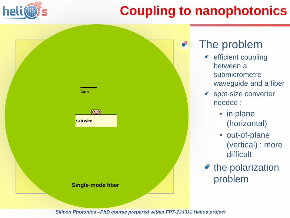
The problemefficient coupling between a submicrometre waveguide and a fiberspot-size converter needed :
• in plane (horizontal)
• out-of-plane (vertical) : more difficult
the polarization problem
Single-mode fiber
1µm
SOI wire
Silicon Photonics –PhD course prepared within FP7-224312 Helios project

Overview
IntroductionHorizontal incoupling: inverted tapersVertical incoupling: grating couplers
operating principlesthe base lineimproving efficiency, bandwidth, polarizationfiber arrays and packaging
Using grating couplersbasic measurements with fiberswafer-scale testingfor free-space communication
ConclusionSilicon Photonics –PhD course prepared within FP7-224312 Helios project

Fiber-chip couplingRegular (planar) taper
Multi-modeFacet coating requiredNo vertical matching
3-D taperDifficult to fabricateWafer scale?
Silicon Photonics –PhD course prepared within FP7-224312 Helios project

The inverted taper
Narrow waveguide tipmode is ‘squeezed out’ of corecaptured by overlay waveguide
High NAfiber
inverted taper
to circuit
Silicon Photonics –PhD course prepared within FP7-224312 Helios project

The inverted taper
Broad wavelength rangeSingle modeEasy to fabricate (if you can make the tips)Low facet reflections
inverted taper
to circuit
Shoji et al. EL 38, p.1669 (2002)McNab et al. OpEx 11(22), P. 2927 (2003)
Silicon Photonics –PhD course prepared within FP7-224312 Helios project


Coupling for both polarizations
(lensed fiber mfd 3.5µm)
Silicon Photonics –PhD course prepared within FP7-224312 Helios project

XY alignment tolerances SiNx waveguide (3µm x 3µm) 3µm fiber-spot
1dB: 1µm3µm
3µm
XY Alignment tolerances
Silicon Photonics –PhD course prepared within FP7-224312 Helios project

Both polarizations?
Inverted taper coupler couples both polarizationsTE and TM in the photonic wire
BUT: photonic wires are very polarization sensitiveYou want just one polarization in your wire
Solutionpolarization splitterpolarization-diversity approach
inverted taper
to circuit
Silicon Photonics –PhD course prepared within FP7-224312 Helios project

Polarization diversity
Process both polarizations separatelysplit polarizationsconvert to the same polarization on the chipcombine polarization back into the fiber
two identical circuits
TE/TM
TMTE
TETM
TE/TM TE/TM
Silicon Photonics –PhD course prepared within FP7-224312 Helios project

Polarization splitter/rotator
Short, efficient deviceNot trivial to make (multi-layer, sharp tips)
Watts et al, OL 30(9), p.937 (2005)TE/TM
TM
TETE
Silicon Photonics –PhD course prepared within FP7-224312 Helios project

Horizontal coupling
High coupling efficiencyBroadband operationWorks for both polarizations
But:Large footprint on a ‘nanophotonic’ chipRequires post-processing
• dicing and polishing• no wafer-scale testing possible
Alignment tolerances• larger spot is larger gives better tolerances• larger spot is harder to fabricate• larger spot needs longer taper
inverted taper
to circuit
Silicon Photonics –PhD course prepared within FP7-224312 Helios project

Overview
IntroductionHorizontal incoupling: inverted tapersVertical incoupling: grating couplers
operating principlesthe base lineimproving efficiency, bandwidth, polarizationfiber arrays and packaging
Using grating couplersbasic measurements with fiberswafer-scale testingfor free-space communication
ConclusionSilicon Photonics –PhD course prepared within FP7-224312 Helios project
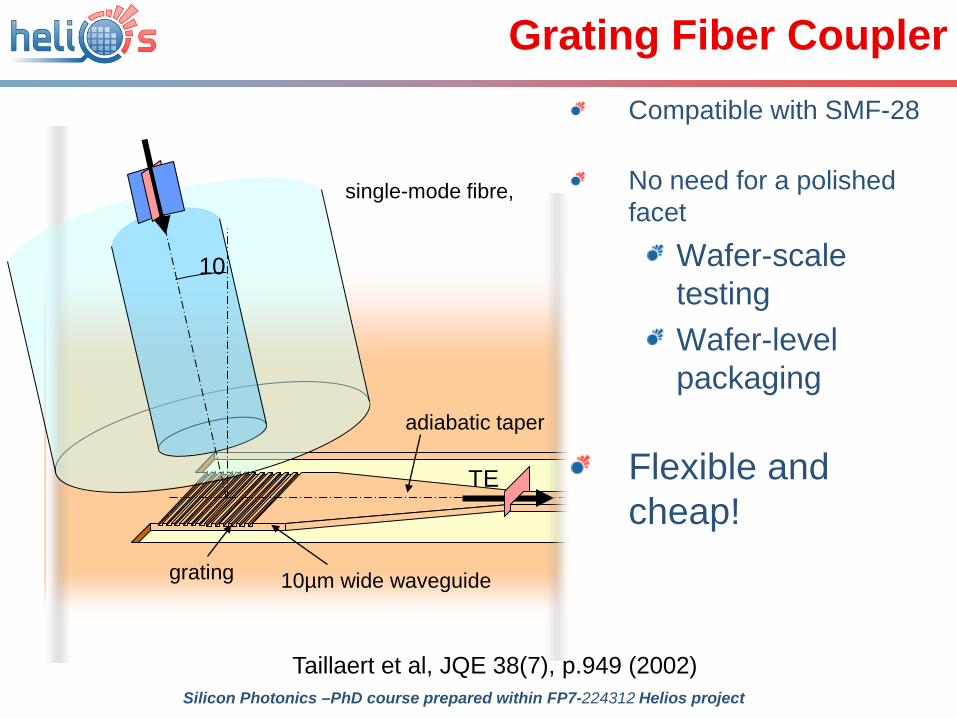
10
TE
Grating Fiber CouplerCompatible with SMF-28
No need for a polished facet
Wafer-scale testing Wafer-level packaging
Flexible and cheap!
adiabatic taper
10µm wide waveguidegrating
single-mode fibre,
Taillaert et al, JQE 38(7), p.949 (2002)Silicon Photonics –PhD course prepared within FP7-224312 Helios project

Operating principle
superstrateradius = k0nsup
K=2π/Λ
substrateradius = k0nsub
kz
Λ
βz
β

1-D grating coupler
Experimental results (λ=630nm,depth=70nm, TE pol.)31 % efficiency (5.1 dB coupling loss)40nm 1dB bandwidth
Also acts as a broadband filter
deep trench
shallow grating
Taillaert et al. JJAP 45(8A), p.6071 (2006)Silicon Photonics –PhD course prepared within FP7-224312 Helios project

Bogaerts et al. JLT 23(1), p.401 (2005)
Fabrication
Fabrication with CMOS toolsdeep UV litho (193nm) + dry etch + strip
• shallow etch (gratings)• deep etch (waveguides)
Overlay alignment: ~15nm
deep trench
shallow grating
Silicon Photonics –PhD course prepared within FP7-224312 Helios project

10
TE
Grating Fiber Coupler
What aboutEfficiency?Alignment tolerance?Optical bandwidth?Polarization dependence?Footprint? Packaging?
adiabatic taper
10µm wide waveguidegrating
single-mode fibre,
Silicon Photonics –PhD course prepared within FP7-224312 Helios project

Coupling efficiencyEfficiency is determined by two factors
Directionality: Fraction sent to the right diffraction orderMode matching: diffracted field profile vs. fiber mode
Taillaert et al., OL 29(23), p.2749 (2004) Silicon Photonics –PhD course prepared within FP7-224312 Helios project

Directionality
Second-order grating: K = βElegant: Vertical outcouplingBackreflection!
superstrate
substrate
K=2π/Λ
β
BACKREFLECTION!
TE
Silicon Photonics –PhD course prepared within FP7-224312 Helios project

Cancel out backreflection
Additional backreflector in front of gratingcancels out grating reflectionwavelength dependentvery accurate positioning required!
Roelkens et al, OL 32(11), p.1495 (2007)
incident
coupled
backreflected
additionalreflector
Silicon Photonics –PhD course prepared within FP7-224312 Helios project

10
TE
Directionality
Detuned second-order grating: K < βOutcoupling in the same direction as waveguide
square grating: most coupling in first ordersome residual coupling in second order
superstrate
substrate
K=2π/Λ
β
Silicon Photonics –PhD course prepared within FP7-224312 Helios project
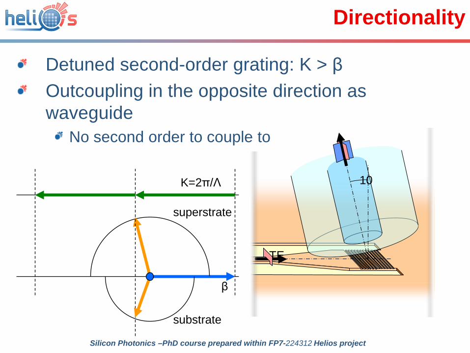
Directionality
Detuned second-order grating: K > βOutcoupling in the opposite direction as waveguide
No second order to couple to
superstrate
substrate
K=2π/Λ
β
10
TE
Silicon Photonics –PhD course prepared within FP7-224312 Helios project

Directionality
First diffraction order: to top and bottom
Select only the top oneSuppress the bottom one
superstrate
substrate
K=2π/Λ
β
2µm SiO2
silicon substrate
220nm Si
Silicon Photonics –PhD course prepared within FP7-224312 Helios project

Directionality
Extended grating teethextra degree of freedom, break symmetry
Roelkens et al, OpEx 14(24), p.11622 (2006)
2µm SiO2
silicon substrate
220nm Si
380nm teeth
Silicon Photonics –PhD course prepared within FP7-224312 Helios project

Directionality condition
Constructive Interference Δφ = 2π
Δφ = πDestructive Interference
D1 D2W2W1
Δφ = 2π
Δφ = π
Silicon Photonics –PhD course prepared within FP7-224312 Helios project

Extended grating teeth: epitaxy Uniform grating defined in Silicon overlay
simulations: 80% coupling efficiency possible First Demonstration with good results:
Epitaxially grown Silicon (LETI) 55% coupling efficiency -1dB/3dB bandwidth of 50nm/100nm
Roelkens et al., IPNRA 2008Silicon Photonics –PhD course prepared within FP7-224312 Helios project

Extended teeth: deposition + etching
2µm SiO2
silicon substrate
220nm Siβ
amorphous/poly-silicon
D. Vermeulen, GFP 2009, PD1

MeasurementsCoupling efficiency = -1.6 dB (68%)
-5.0
-4.5
-4.0
-3.5
-3.0
-2.5
-2.0
-1.5
-1.0
-0.5
0.0
1510 1520 1530 1540 1550 1560 1570
Inse
rtio
n lo
ss fo
r 1 c
oupl
er [d
B]
Wavelength [nm]
D. Vermeulen, GFP 2009, PD1

Poly-Si vs. amorphous Si Wavelength shift due to refractive index difference a-Si poly-Si Coupling efficiency is of the same order
-6
-5.5
-5
-4.5
-4
-3.5
-3
-2.5
-2
-1.5
1470 1490 1510 1530 1550 1570
Cou
plin
g Ef
ficie
ncy
(dB
)
Wavelength (nm)
a-Si overlay poly-Si overlay
D. Vermeulen, GFP 2009, PD1
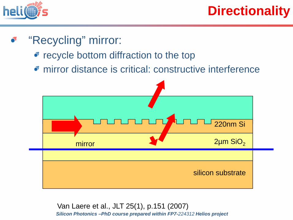
Directionality
“Recycling” mirror:recycle bottom diffraction to the topmirror distance is critical: constructive interference
Van Laere et al., JLT 25(1), p.151 (2007)
2µm SiO2
silicon substrate
220nm Si
mirror
Silicon Photonics –PhD course prepared within FP7-224312 Helios project

Adding a “bottom” mirror
Make a top mirrorBCB spin coating + gold evaporationTransfer circuit to other carrier + substrate removal
Van Laere et al., JLT 25(1), p.151 (2007)
BCB spin-coat
2µm SiO2
silicon substrate
220nm Si
Gold mirror
Silicon Photonics –PhD course prepared within FP7-224312 Helios project
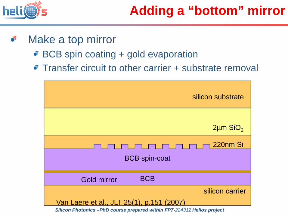
BCB
silicon carrier
Adding a “bottom” mirror
Make a top mirrorBCB spin coating + gold evaporationTransfer circuit to other carrier + substrate removal
Van Laere et al., JLT 25(1), p.151 (2007)
BCB spin-coat
220nm Si
Gold mirror
Silicon Photonics –PhD course prepared within FP7-224312 Helios project
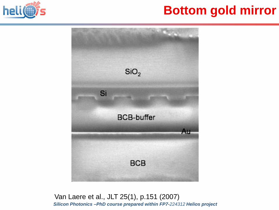
Bottom gold mirror
Van Laere et al., JLT 25(1), p.151 (2007) Silicon Photonics –PhD course prepared within FP7-224312 Helios project

Bottom gold mirrorGold bottom mirror:
mirror on top of gratingupside down on carriersubstrate removal
70% efficiency (-1.5dB)
Van Laere et al., JLT 25(1), p.151 (2007) Silicon Photonics –PhD course prepared within FP7-224312 Helios project

Silicon bottom mirror
Bottom Distributed Bragg mirrorNot possible with crystalline SOIPossible with high-quality amorphous silicon
silicon substrate
220nm aSi
Selvaraja et al. CLEO/IQEC 2009
aSi DBR
Silicon Photonics –PhD course prepared within FP7-224312 Helios project

Silicon bottom mirrorSilicon bottom mirror: DBR
Replacement of gold by a SiO2/a-Si DBR Deposited amorphous Silicon waveguide (no bonding)Coupling efficiency: 70% (-1.5dB)
DBR mirror
Selvaraja et al. CLEO/IQEC 2009Silicon Photonics –PhD course prepared within FP7-224312 Helios project

Coupling efficiencyEfficiency is determined by two factors
Directionality: Fraction sent to the right diffraction orderMode matching: diffracted field profile vs. fiber mode
Silicon Photonics –PhD course prepared within FP7-224312 Helios project

Modal overlap
Mismatch between diffracted field and fiber mode
fiber mode
diffractedintensity
Penalty > 1dB
Taillaert et al., OL 29(23), p.2749 (2004) Silicon Photonics –PhD course prepared within FP7-224312 Helios project

Optimized onuniform grating
Optimized : > 90% efficiency
Challenging to fabricatesmallest groove width is 30nm, but can be increased to 60nm with only 1-2 percent decreased efficiencybottom reflector (when using regular SOI the efficiency is 63%)
narrow grooves(weak coupling) broad grooves (50%)
DBR for directionality
Taillaert et al., OL 29(23), p.2749 (2004) Silicon Photonics –PhD course prepared within FP7-224312 Helios project

Optimized nonuniform grating
Efficiency versus wavelength
1500 1520 1540 1560 1580 1600
0.2
0.3
0.4
0.5
0.6
0.7
0.8
0.9
1SOISOI+DBR
wavelength (nm)
effic
ienc
y
1dB coupling loss
> 90%
> 60%
Taillaert et al., OL 29(23), p.2749 (2004) Silicon Photonics –PhD course prepared within FP7-224312 Helios project

10
TE
Grating Fiber Coupler
What aboutEfficiency?Alignment tolerance?Optical bandwidth?Polarization dependence?Footprint? Packaging?
adiabatic taper
10µm wide waveguidegrating
single-mode fibre,
Silicon Photonics –PhD course prepared within FP7-224312 Helios project

Diffraction grating: alignmentGood alignment tolerances are achieved since we are aligning modes with a mode field diameter of about 10µm!
Alignment sensitivity measurement
diameter of the -0.5dB contour is 2µm
10
TE
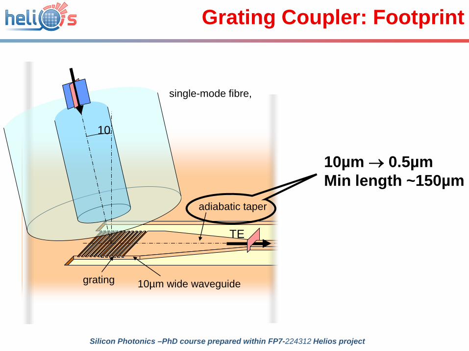
Grating Coupler: Footprint
adiabatic taper
10µm wide waveguidegrating
single-mode fibre,
10µm → 0.5µmMin length ~150µm
Silicon Photonics –PhD course prepared within FP7-224312 Helios project

Adiabatic taper
“Adiabatic” Taper of 10µm to 1µm
0 10 20 30 40 50 60
0.2
0.4
0.6
0.8
1
Taper length [µm]
Tran
smis
sion
parabolic
linear
Silicon Photonics –PhD course prepared within FP7-224312 Helios project

Focusing grating couplersCurved gratings: focus light in submicron waveguides
No adiabatic transition neededGrating in linear taperGrating in slab, focus on low-contrast aperture
Van Laere et al, PTL 19(23), pp. 1921 (2005)Silicon Photonics –PhD course prepared within FP7-224312 Helios project

Focusing grating couplers
Grating in taperfocusing on taper point
Grating in slabFocusing on waveguide aperture (shallow etched)
Van Laere et al, PTL 19(23), pp. 1921 (2005)Silicon Photonics –PhD course prepared within FP7-224312 Helios project

Focusing grating couplers
Van Laere et al, PTL 19(23), pp. 1921 (2005)Silicon Photonics –PhD course prepared within FP7-224312 Helios project

Diffraction gratings: bandwidthTypical bandwidth of a grating coupler
Gaussian coupling spectrum1dB bandwidth of a single grating coupler: 40-50nm3dB bandwidth of a single grating coupler: 50-100nm
1dB bandwidth
3dB bandwidth
Silicon Photonics –PhD course prepared within FP7-224312 Helios project

Diffraction gratings: bandwidthBandwidth is sufficient for a single wavelength bandSome applications require two wavelength bands
• e.g. in FTTH, use of 1310nm and 1490nm/1550nm for upstream and downstream communication
Roelkens et al.OpEx 15(16), p.10091 (2007)
see posterD. Vermeulen
Silicon Photonics –PhD course prepared within FP7-224312 Helios project

FTTH Duplexer
Using a simple grating coupler(only 70nm etch, no overlay)Overall coupling efficiency: -7dB/coupler
-16
-14
-12
-10
-8
-6
-4
-2
0
1200.00 1300.00 1400.00 1500.00 1600.00wavelength [nm]
coup
ling
effic
ienc
y [d
B]
1490nm
1550nm1310nm
Vermeulen et al. ECOC2008 Tu.3.C.6
see posterD. Vermeulen
Silicon Photonics –PhD course prepared within FP7-224312 Helios project

10
TE
Grating Coupler: Polarization
adiabatic taper
10µm wide waveguidegrating
single-mode fibre,
Only one fiberpolarization is
coupled
Silicon Photonics –PhD course prepared within FP7-224312 Helios project

10
TM
Grating Coupler for TM
Different parameters thanfor TE gratings
TM mode has lower βTM grating has larger pitch:
1040nm instead of 630nm
Silicon Photonics –PhD course prepared within FP7-224312 Helios project

TM coupler - efficiency
-30
-25
-20
-15
-10
1500 1520 1540 1560 1580 1600
Wavelength [nm]
Effi
cien
cy [d
B]
Fiber to fiber efficiency
25% per coupler
Silicon Photonics –PhD course prepared within FP7-224312 Helios project
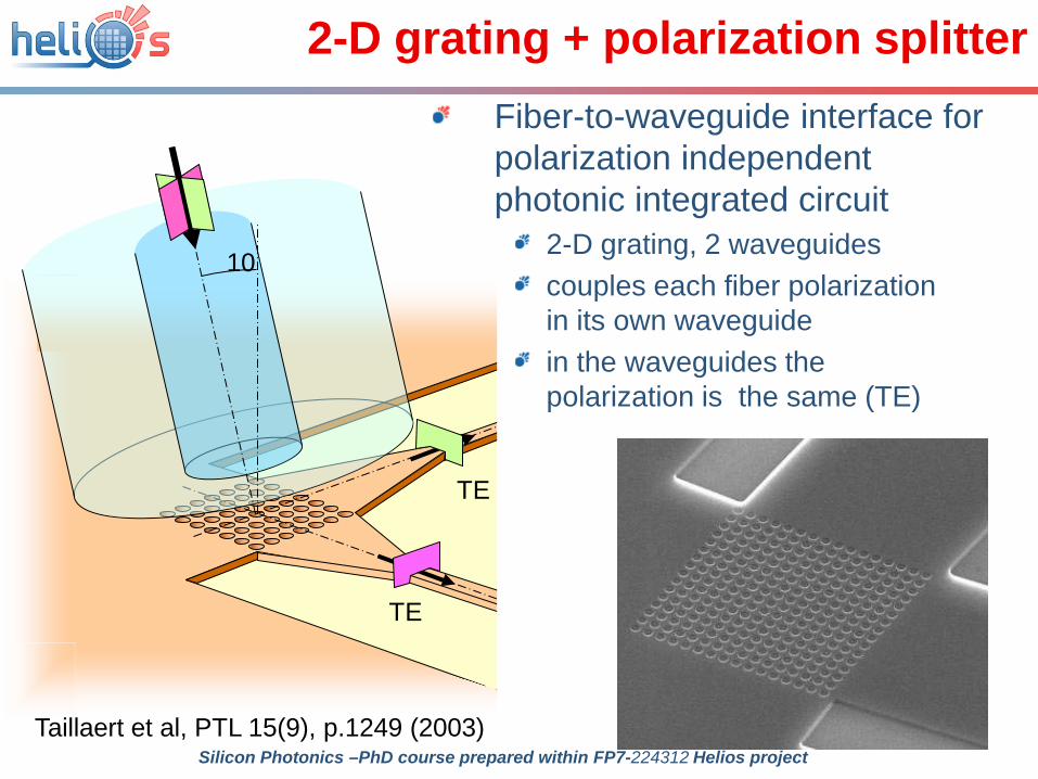
2-D grating + polarization splitter
TE
TE
10
Taillaert et al, PTL 15(9), p.1249 (2003)
Fiber-to-waveguide interface for polarization independent photonic integrated circuit
2-D grating, 2 waveguidescouples each fiber polarizationin its own waveguidein the waveguides thepolarization is the same (TE)
Silicon Photonics –PhD course prepared within FP7-224312 Helios project

2-D fiber couplers
Efficiency: -6.7dB (21%)Extinction ratio: > 18dB3dB bandwidth: 60nm
-11
-10
-9
-8
-7
-6
1510 1520 1530 1540 1550 1560 1570 1580wavelength [nm]
tran
smis
sion
of s
ingl
e fib
er c
oupl
er [d
B]
60nm
-6.7dB
10µm
Bogaerts et al.OpEx 15(4), p.1567 (2007) Silicon Photonics –PhD course prepared within FP7-224312 Helios project

on-chip components are polarisation dependent
fiber-to-fiber transmission is polarisation independent
Polarisation Diversity Circuit
y-polarization
split polarisations
light in
identicalcircuits
x-polarization
x
yz
xy
light out
single-modefiber
2-D grating
combine polarisations
2-D grating

10
TE
Grating Fiber Coupler
What aboutAlignment toleranceEfficiencyOptical bandwidthPolarization dependenceFootprint
We can fix each of these, but fix all together?adiabatic taper
10µm wide waveguidegrating
single-mode fibre,
YES! Different tricks can be combined
Silicon Photonics –PhD course prepared within FP7-224312 Helios project

2-D focusing grating couplers
2-D grating = 2 1-D grating1-D curved grating linesPlace hole at intersection25% efficiency!
Van Laere et al, JLT, to be publishedSilicon Photonics –PhD course prepared within FP7-224312 Helios project

2-D focusing grating couplers
Experimental results25% coupling efficiency(better than non-curved)
Van Laere et al, JLT, to be publishedSilicon Photonics –PhD course prepared within FP7-224312 Helios project

10um fiber core
waveguides
Grating coupler
Luxtera gratings
Silicon Photonics –PhD course prepared within FP7-224312 Helios project

Luxtera grating couplers
Demonstrated performance:– 0.8 dB loss to/from fiber

Grating Coupler Evolution
Wavelength (μm)
Inse
rtion
Los
s (d
B) Today’s
D.O.R.
Firstdesign
Seconddesign
Thirddesign
Bestdesign
Silicon Photonics –PhD course prepared within FP7-224312 Helios project
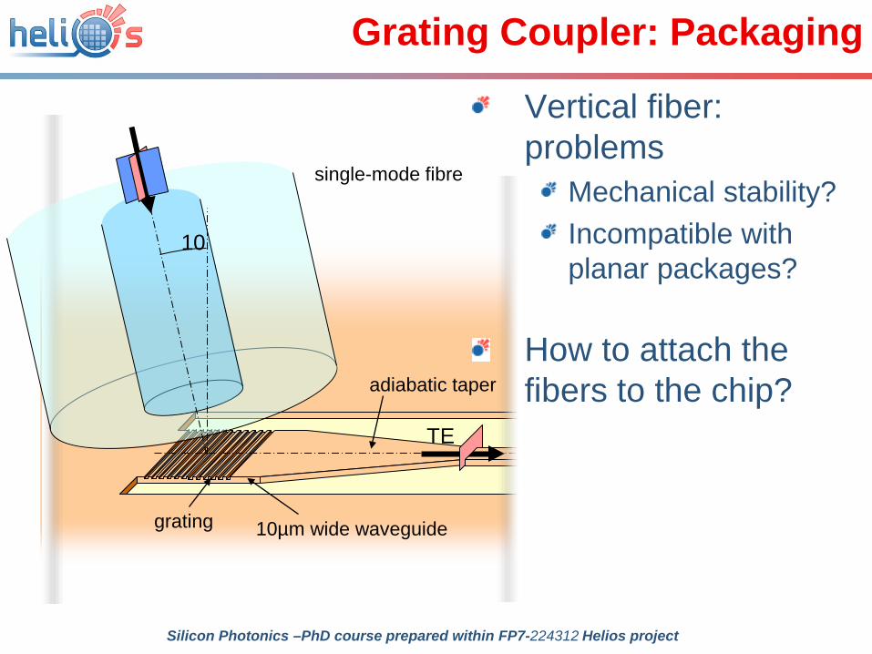
10
TE
Grating Coupler: Packaging
Vertical fiber: problems
Mechanical stability?Incompatible with planar packages?
How to attach the fibers to the chip?adiabatic taper
10µm wide waveguidegrating
single-mode fibre
Silicon Photonics –PhD course prepared within FP7-224312 Helios project

Just glue?
Very accurateActive alignmentUV curing(even through the fiber)
ButNot very practicalMechanically unstable
Silicon Photonics –PhD course prepared within FP7-224312 Helios project

10
TE
Grating Coupler: Packaging
Vertical fiber: problemsMechanical stability?Incompatible with planar packages?
For many purposes, the fibers should be horizontal
adiabatic taper
10µm wide waveguidegrating
single-mode fibre
Silicon Photonics –PhD course prepared within FP7-224312 Helios project

Horizontal fiber
Use angle-polished fiber (array)
TE
10 total internal
reflection
50 polishangle
Silicon Photonics –PhD course prepared within FP7-224312 Helios project

10
TE
Many fibers?
Multiple fibers?
adiabatic taper
10µm wide waveguidegrating
single-mode fibre
Silicon Photonics –PhD course prepared within FP7-224312 Helios project

Fiber arrays
1-D rows of fibersTypical pitch = 125µm or 250µmPositioning must be accurateexample: Silicon V-grooves
Silicon Photonics –PhD course prepared within FP7-224312 Helios project

Array-connected SOI circuit4 x 4 wavelength router
Standard connector with 8 fibers (4 input, 4 output)Vertical fiber couplers4 x 4 AWG
Dumon et al.,OpEx 14(2), p.664 (2006) Silicon Photonics –PhD course prepared within FP7-224312 Helios project

• coupling to fully passive SOI chip
T. Tekin et al. ECOC 2008,P.2.21
Fiber array package - concept
Silicon Photonics –PhD course prepared within FP7-224312 Helios project

uv-curingepoxy
fiber-array
SOI chip
Si v-groovebase
glass
uv-curingepoxy
fiber-array
SOI chip
Si v-groovebase
glass
uv-curingepoxy
fiber-array
SOI chip
uv-curingepoxy
uv-curingepoxy
fiber-array
SOI chip
uv-curingepoxy
T. Tekin et al. ECOC 2008,P.2.21
8 fiber array package

Silicon Photonics –PhD course prepared within FP7-224312 Helios project

Example – g-Pack
Silicon Photonics –PhD course prepared within FP7-224312 Helios project
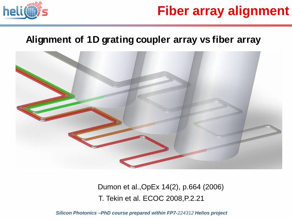
Alignment of 1D grating coupler array vs fiber array
T. Tekin et al. ECOC 2008,P.2.21Dumon et al.,OpEx 14(2), p.664 (2006)
Fiber array alignment
Silicon Photonics –PhD course prepared within FP7-224312 Helios project

V-groove based 8 fiber array - specifications
1 2 3 4 5 6 7 8
Fiber array tolerances
Silicon Photonics –PhD course prepared within FP7-224312 Helios project

Fiber array – position scanXY-Scanned Fiber Positions1-3 and 6-8
Fiber array tolerances
Silicon Photonics –PhD course prepared within FP7-224312 Helios project

Grating Coupler: Density
Fiber density?Fiber pitch: 125 or 250µmCoupler pitch can be as low as 25µmWaste of expensive chip real-estateImpact on yield
Useful chip area
Waste of space
Silicon Photonics –PhD course prepared within FP7-224312 Helios project

Silicon vs. silica density
Silicon photonics40 channel AWGFootprint 1 1mm2
fiber array width: 5-6mm2
Area loss: 90%
Silica technologysimilar core/spacing as fibersNo fan-out required
Fiber pitch = 127 µm ~ 6mm
Silicon Photonics –PhD course prepared within FP7-224312 Helios project

Photonic interposer
Silica-based interposer chipFan-out of photonic waveguides to fiber arrayFan-out of electronic connection to wire bond pads
Silicon chip can be kept small (cost, yield)One interposer design can serve many chip layouts
Silicon Photonics –PhD course prepared within FP7-224312 Helios project

Coupling to the interposer
Use TIR mirror to couple to the silica waveguideDifficult to fabricate!
silicon carrier
SOI photonic chip
Silicon Photonics –PhD course prepared within FP7-224312 Helios project
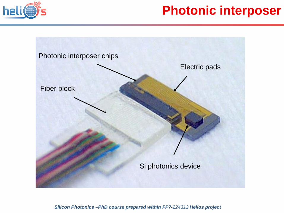
Photonic interposer
Si photonics device
Photonic interposer chips
Fiber block
Electric pads
Silicon Photonics –PhD course prepared within FP7-224312 Helios project

Overview
IntroductionHorizontal incoupling: inverted tapersVertical incoupling: grating couplers
operating principlesthe base lineimproving efficiency, bandwidth, polarizationfiber arrays and packaging
Using grating couplersbasic measurements with fiberswafer-scale testingfor free-space communication
ConclusionSilicon Photonics –PhD course prepared within FP7-224312 Helios project

Using vertical coupling
Easy measurements
Wafer-scale testingWith array probeWith grating probe
Free-space couplingCamera measurementsRetroreflective chipsBeam steering and forming
10
TE
adiabatic taper
10µm wide waveguidegrating
single-mode fibre
Silicon Photonics –PhD course prepared within FP7-224312 Helios project

Start measuring in 5 minutes
Silicon Photonics –PhD course prepared within FP7-224312 Helios project

Wafer-scale testingDiffraction gratings allow for wafer-scale testing of photonic integrated circuits
• A modified electrical wafer prober can be used for this purpose, e.g. Luxtera
• This does not allow probing of individual components in a complex photonic integrated circuit!
Silicon Photonics –PhD course prepared within FP7-224312 Helios project

Optical probing
10
TE
Fixed location: can only testcircuits which have fiber
coupler input/outputs
Silicon Photonics –PhD course prepared within FP7-224312 Helios project

Optical probeNeed for a true equivalent of an electrical probe
Allows for testing of individual components in a PIC without the need for dedicated coupling structures on the PICOptical fiber with a diffraction grating (gold stripes) defined on the core of the optical fiberFabricated using a nano-imprint and transfer technique
Scheerlinck et al.APL 92(3), p.031104 (2008)Silicon Photonics –PhD course prepared within FP7-224312 Helios project
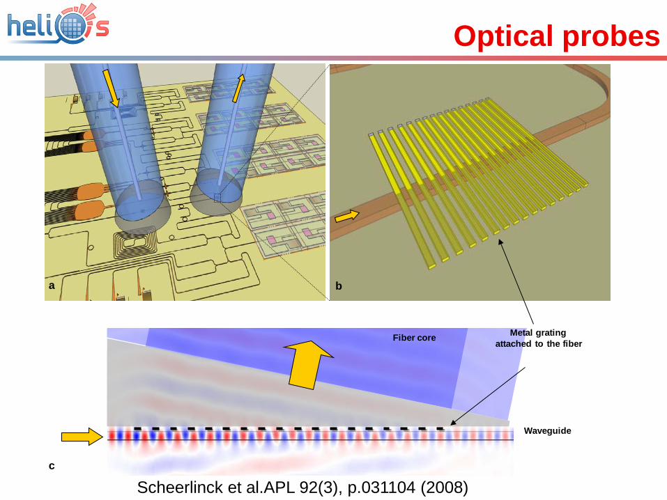
Optical probes
Scheerlinck et al.APL 92(3), p.031104 (2008)c
Fiber core
Waveguide
a b
Metal gratingattached to the fiber
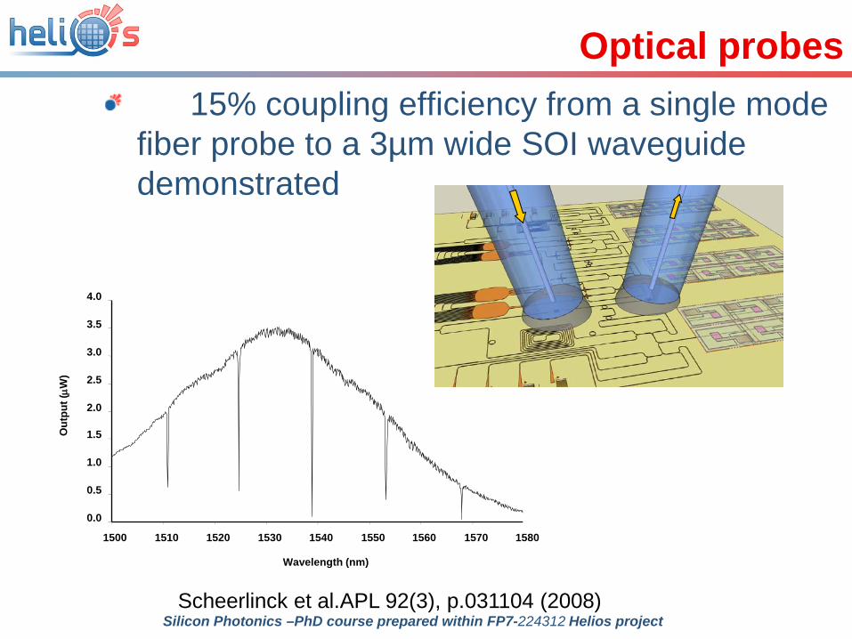
Optical probes15% coupling efficiency from a single mode
fiber probe to a 3µm wide SOI waveguide demonstrated
0.0
0.5
1.0
1.5
2.0
2.5
3.0
3.5
4.0
1500 1510 1520 1530 1540 1550 1560 1570 1580
Wavelength (nm)
Out
put (µW
)
Scheerlinck et al.APL 92(3), p.031104 (2008)Silicon Photonics –PhD course prepared within FP7-224312 Helios project
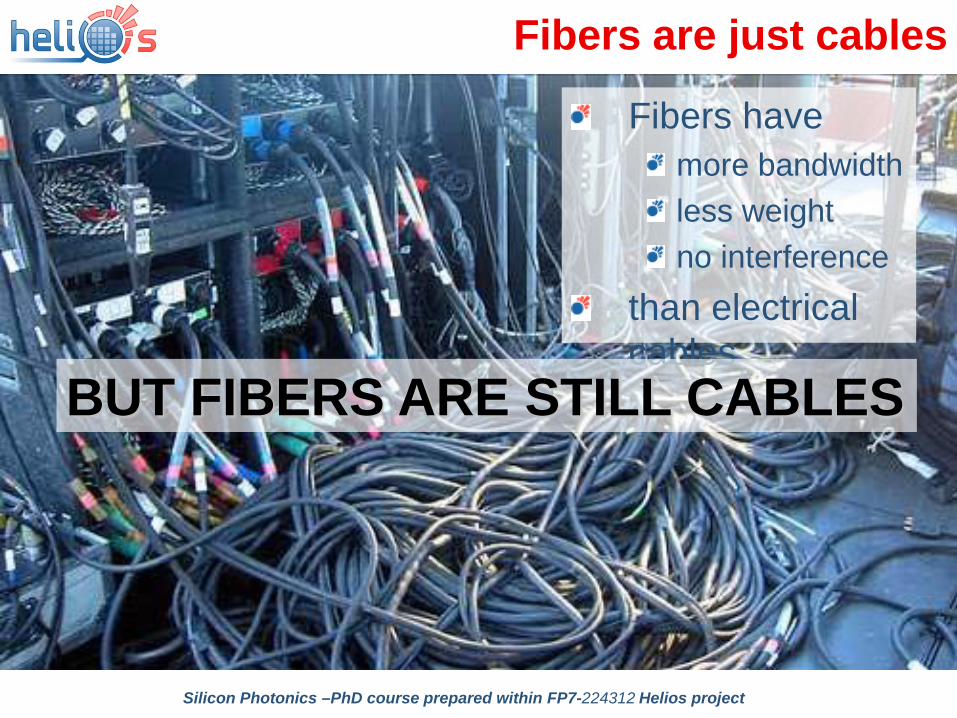
Fibers are just cables
Fibers havemore bandwidthless weightno interference
than electrical cables
BUT FIBERS ARE STILL CABLES
Silicon Photonics –PhD course prepared within FP7-224312 Helios project

Wireless photonics?
Free-space interfaces for photonic ICs?
Useful forremote readoutmassive parallel sensingtracking, identificationmedical diagnostics...
Main limitationsline of sightpower budget
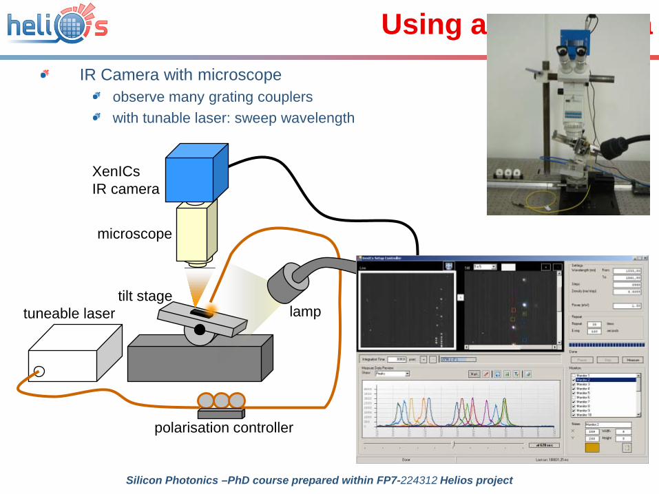
Using an IR cameraIR Camera with microscope
observe many grating couplerswith tunable laser: sweep wavelength
tuneable lasertilt stage
microscope
XenICsIR camera
polarisation controller
lamp
Silicon Photonics –PhD course prepared within FP7-224312 Helios project

Camera setup
Silicon Photonics –PhD course prepared within FP7-224312 Helios project

Camera measurements
Readout system
massively parallelNo density problem2-D arrays possible
Silicon Photonics –PhD course prepared within FP7-224312 Helios project
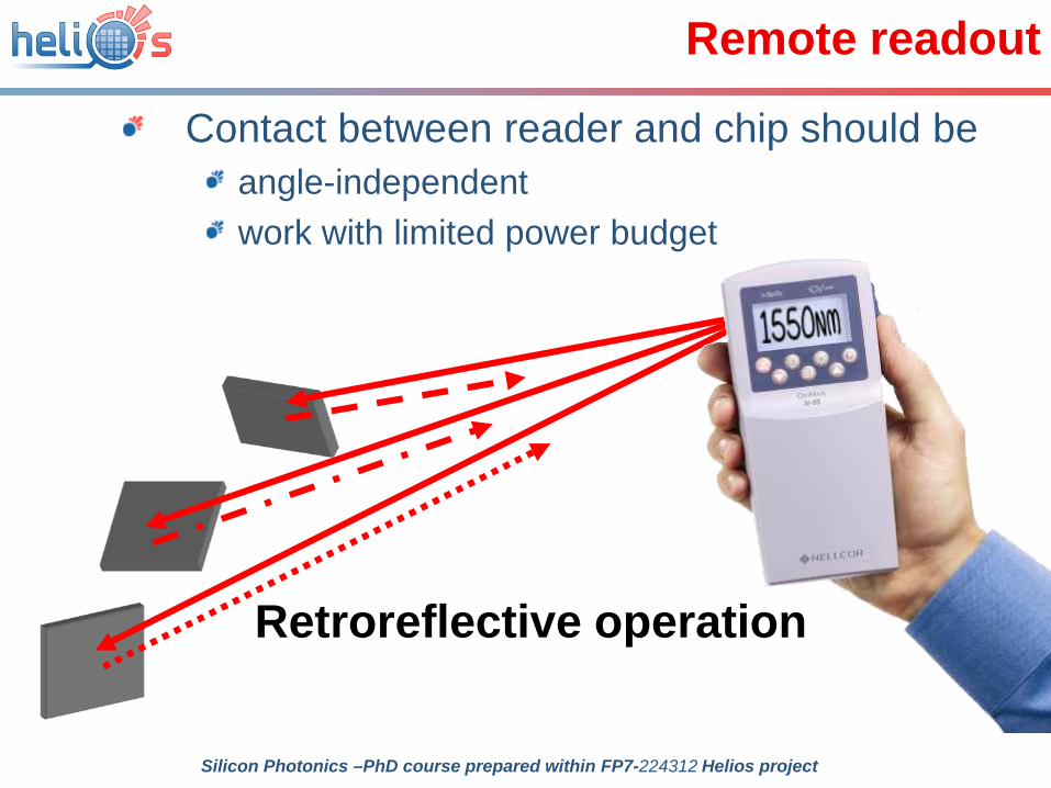
Remote readout
Contact between reader and chip should beangle-independentwork with limited power budget
Retroreflective operation
Silicon Photonics –PhD course prepared within FP7-224312 Helios project

Free-space retroreflectivity
Retroreflective: use same grating coupler for input and output
Verbist et al. IEEE/LEOS Benelux Symposium 2008 p.171Silicon Photonics –PhD course prepared within FP7-224312 Helios project

Butterfly chip
Solution: duplicate filter circuits
curvedgrating couplersfor different angles
identical filtercircuits
varyorientation
vary tilt angle
Verbist et al. IEEE/LEOS Benelux Symposium 2008 p.171Silicon Photonics –PhD course prepared within FP7-224312 Helios project

Results
Clear resonancespectrum from fiber coupler
Verbist et al. IEEE/LEOS Benelux Symposium 2008 p.171Silicon Photonics –PhD course prepared within FP7-224312 Helios project

Results
Resonance is evenvisible in multiplecouplers and from the entire chip
Coupler ACoupler B (other tilt)Entire chip
AB
Verbist et al. IEEE/LEOS Benelux Symposium 2008 p.171Silicon Photonics –PhD course prepared within FP7-224312 Helios project
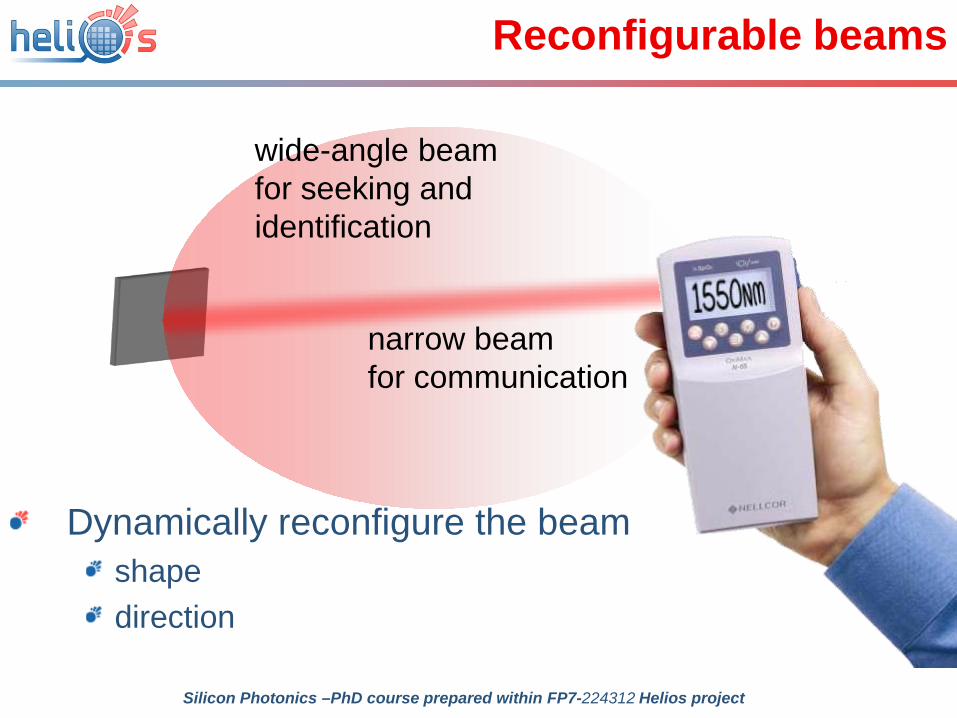
Reconfigurable beams
Dynamically reconfigure the beamshapedirection
wide-angle beamfor seeking andidentification
narrow beamfor communication
Silicon Photonics –PhD course prepared within FP7-224312 Helios project

Phased arrays
1 grating coupler = patch antennaMany grating couplers = synthetic antennaPhase between different couplers controls
direction (beam steering)shape (beam shaping)
grating
heaters forphase control
Silicon
Silicon Photonics –PhD course prepared within FP7-224312 Helios project
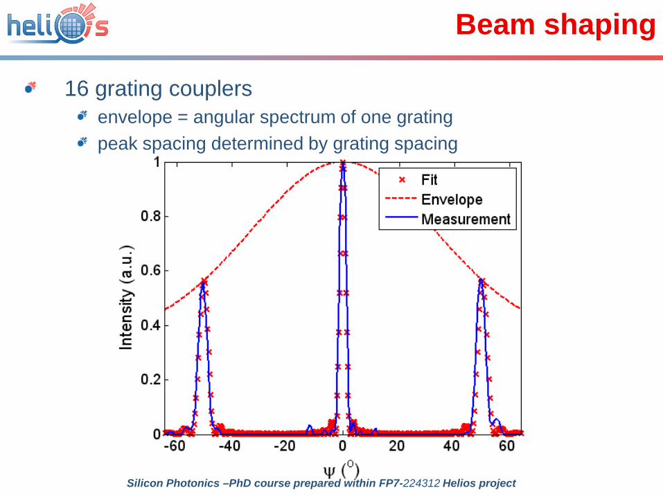
Beam shaping
16 grating couplersenvelope = angular spectrum of one gratingpeak spacing determined by grating spacing
Silicon Photonics –PhD course prepared within FP7-224312 Helios project

Beam Steering
Current through heaters shifts beam
Silicon Photonics –PhD course prepared within FP7-224312 Helios project

Horizontal vs. VerticalHorizontal Vertical
Alignment tolerance + ++Efficiency +++ ++(+)Polarisation +++ ++(+)Bandwidth ++ +Fabrication + ++Packaging +++ ++Wafer-scale testing --- +++Footprint --- +++Density --- +++
Free-space -- +++

Summary
Coupling to submicron silicon waveguides = difficultHorizontal: mode expandersVertical: grating couplers
Functional issues: polarisation, efficiency, bandwidthhorizontal still outperforms verticalvertical has different tricks up its sleeve
Practical issues: tolerances, footprint, testingvertical outperforms horizontal
Applicationsfiber connectionsfree space
Silicon Photonics –PhD course prepared within FP7-224312 Helios project

Collaboration works…
Much of this work was donein collaborative projects…
The European Union • IST-PICCO • IST-PICMOS• IST-ePIXnet• ICT WaDiMOS• ICT HELIOS
The European Space AgencyBelgian Science Policy
• IAP-V/18 PHOTON network• IAP-6/10 Photonics@be
Silicon Photonics –PhD course prepared within FP7-224312 Helios project

Coupling light is not trivial…
So you’re convinced that there should be
some light coming through?
Silicon Photonics –PhD course prepared within FP7-224312 Helios project


![Silicon Photonics Circuit Design: Methods, Tools and ... · tlenecks [2,56]. Photonic-electronic co-integration and co-design will make it possible to create integrated photonic-electronic-software](https://static.fdocuments.net/doc/165x107/5e95fd09160d7b469b489eee/silicon-photonics-circuit-design-methods-tools-and-tlenecks-256-photonic-electronic.jpg)


