Lecture 1 - Tel Aviv Universityhyde.eng.tau.ac.il/Hardware_Algorithms/TAU_2008_Lecture1... ·...
48
Lecture 1: ( © copyright by Daniel Seidner) 1 Lecture 1 מעגל צירופי– הגדרה• אבני הבניין של מעגל צירופי הם שעריand, or, not . הכניסות של השערים הנ" ל סימטריות והם מהווים מערכת אוניברסלית. • מעגל צירופי בנוי מעץ מכוון עם שורש. הקשתות מכוונות מהעלים לשורש. אין בו מעגלים. • בכל צומת של העץ ממוק ם שער– כך נקבעת הפונקציונליות של המעגל. המעגל מבצע חישוב של הפונקציות הבוליאניות שהשערים ממשים ופלט את ערך היציאה המחושב• השהיית המעגל– המסלול הארוך ביותר מעלה לשורש. • מחיר המעגל– מספר הצמתים בעץ. כלומר, מספר השערים בעץ) במעגל.( • הערה: אנו מניחים שלכל השע רים אותה השהייה ואותו מחיר. אפשר היה להוסיף משקל לכל שער. במקרה כזה המחיר היה המשקל הכולל וכו' . • הערה: העלים יכולים להיות מוזנים על- ידי אותם קלטים. • דרגת הכניסה– Fan in – מספר הכניסות לשער. ב חרנו שיהיה2 לכל היותר. ) כדוגמא לכל הנ" ל נראה שערand מרובה כ ניסות( הגדרה חדשה) הרחבת ההגדרה הקודמת( : • נשתמש ב דג במקום בעץ– DAG (Directed Acyclic Graph) • דג אינו עץ. מה שנקרא עלה בעץ נקרא כאן מקור. • מה שנקרא שורש בעץ נקרא כאן בור. • לדג יכולים להיות מספר בורות. ) נראה דוגמאות במהלך ההרצאה(
Transcript of Lecture 1 - Tel Aviv Universityhyde.eng.tau.ac.il/Hardware_Algorithms/TAU_2008_Lecture1... ·...

Lecture 1: ( © copyright by Daniel Seidner) 1
Lecture 1
הגדרה–מעגל צירופי
ל סימטריות והם "הכניסות של השערים הנ. and, or, notאבני הבניין של מעגל צירופי הם שערי • .מהווים מערכת אוניברסלית
.אין בו מעגלים. הקשתות מכוונות מהעלים לשורש. מעגל צירופי בנוי מעץ מכוון עם שורש •
המעגל מבצע חישוב של . כך נקבעת הפונקציונליות של המעגל–ם שער בכל צומת של העץ ממוק • הפונקציות הבוליאניות שהשערים ממשים ופלט את ערך היציאה המחושב
. המסלול הארוך ביותר מעלה לשורש–השהיית המעגל •
).במעגל(מספר השערים בעץ , כלומר. מספר הצמתים בעץ–מחיר המעגל •
.אפשר היה להוסיף משקל לכל שער. רים אותה השהייה ואותו מחיראנו מניחים שלכל השע: הערה • .' המחיר היה המשקל הכולל וכובמקרה כזה
.ידי אותם קלטים-העלים יכולים להיות מוזנים על: הערה •
. לכל היותר2חרנו שיהיה ב. מספר הכניסות לשער – Fan in –דרגת הכניסה • )ניסות מרובה כandל נראה שער "כדוגמא לכל הנ(
:) הרחבת ההגדרה הקודמת (הגדרה חדשה
DAG (Directed Acyclic Graph) –במקום בעץ דג נשתמש ב •
. מה שנקרא עלה בעץ נקרא כאן מקור.דג אינו עץ •
.מה שנקרא שורש בעץ נקרא כאן בור •
.לדג יכולים להיות מספר בורות • )נראה דוגמאות במהלך ההרצאה(
Lecture 1: ( © copyright by Daniel Seidner) 2
1.8 Gates
The basic building blocks which are used to implement a logic function are called gates. Any
equation can be considered as a system having inputs (the variables) and outputs (the result of
applying the functions on the variables). The equation ),,( CBAfY = describes a system
having 3 inputs CBA ,, and a single output Y .
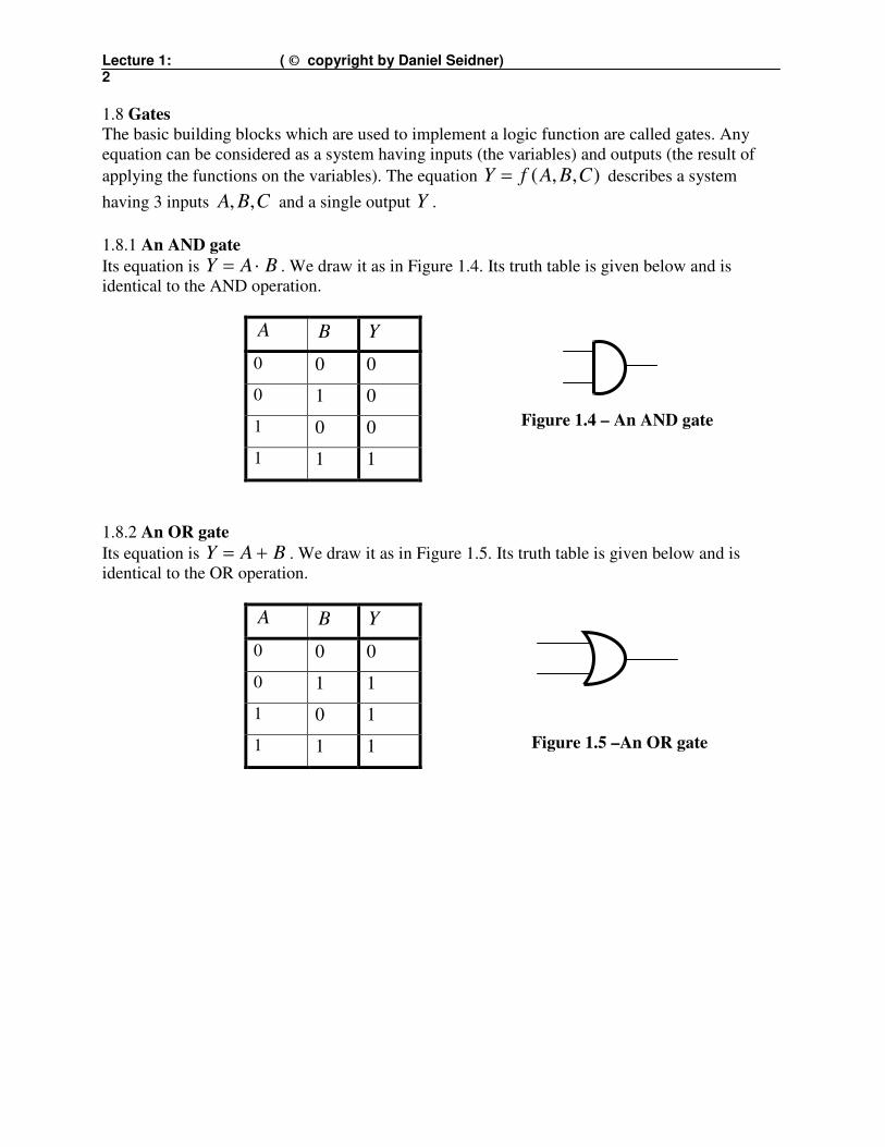
1.8.1 An AND gate
Its equation is BAY ⋅= . We draw it as in Figure 1.4. Its truth table is given below and is
identical to the AND operation.
A B Y
0 0 0
0 1 0
1 0 0
1 1 1
1.8.2 An OR gate
Its equation is BAY += . We draw it as in Figure 1.5. Its truth table is given below and is
identical to the OR operation.
A B Y
0 0 0
0 1 1
1 0 1
1 1 1
Figure 1.4 – An AND gate
Figure 1.5 –An OR gate

Lecture 1: ( © copyright by Daniel Seidner) 3
1.8.3 A NOT gate (usually called an INVERTER)
Its equation is AY = . We draw it as in Figure 1.6. Its truth table is given below and is identical
to the NOT operation.
A Y
0 1
1 0
1.8.4 A NAND gate
Its equation is BAY ⋅= . We draw it as in Figure 1.7. Its truth table is given below.
A B Y
0 0 1
0 1 1
1 0 1
1 1 0
1.8.5 A NOR gate
Its equation is BAY += . We draw it as in Figure 1.8. Its truth table is given below.
A B Y
0 0 1
0 1 0
1 0 0
1 1 0
Figure 1.6 – An Inverter (a NOT gate)
Figure 1.7– A NAND gate
Figure 1.8 – A NOR gate
Lecture 1: ( © copyright by Daniel Seidner) 4
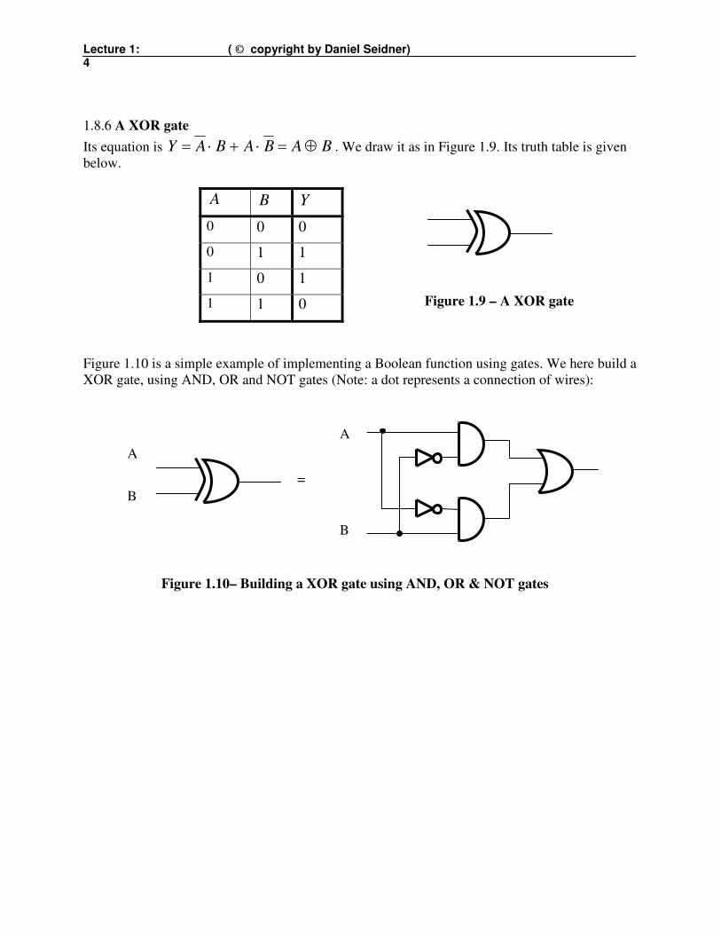
1.8.6 A XOR gate
Its equation is BABABAY ⊕=⋅+⋅= . We draw it as in Figure 1.9. Its truth table is given
below.
A B Y
0 0 0
0 1 1
1 0 1
1 1 0
Figure 1.10 is a simple example of implementing a Boolean function using gates. We here build a
XOR gate, using AND, OR and NOT gates (Note: a dot represents a connection of wires):
Figure 1.9 – A XOR gate
Figure 1.10– Building a XOR gate using AND, OR & NOT gates
A
B
A
B
=
Lecture 1: ( © copyright by Daniel Seidner) 5
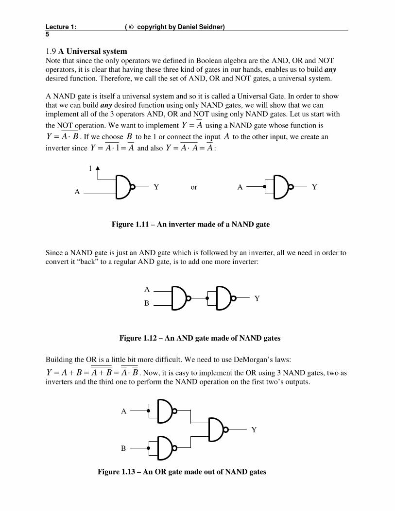
1.9 A Universal system Note that since the only operators we defined in Boolean algebra are the AND, OR and NOT
operators, it is clear that having these three kind of gates in our hands, enables us to build any
desired function. Therefore, we call the set of AND, OR and NOT gates, a universal system.
A NAND gate is itself a universal system and so it is called a Universal Gate. In order to show
that we can build any desired function using only NAND gates, we will show that we can
implement all of the 3 operators AND, OR and NOT using only NAND gates. Let us start with
the NOT operation. We want to implement AY = using a NAND gate whose function is
BAY ⋅= . If we choose B to be 1 or connect the input A to the other input, we create an
inverter since AAY =⋅= 1 and also AAAY =⋅= :
Since a NAND gate is just an AND gate which is followed by an inverter, all we need in order to
convert it “back” to a regular AND gate, is to add one more inverter:
Building the OR is a little bit more difficult. We need to use DeMorgan’s laws:
BABABAY ⋅=+=+= . Now, it is easy to implement the OR using 3 NAND gates, two as
inverters and the third one to perform the NAND operation on the first two’s outputs.
Figure 1.11 – An inverter made of a NAND gate
A
1
Y or A Y
Figure 1.12 – An AND gate made of NAND gates
B Y
A
Figure 1.13 – An OR gate made out of NAND gates
B
Y
A

Lecture 1: ( © copyright by Daniel Seidner) 6
Let us now try to implement a XOR gate using only NAND gates. The easiest way is to replace
any inverter in Figure 1.10 with the inverter of Figure 1.11, and any AND gate with the AND
gate of Figure 1.12, and finally, the OR gate with the OR of Figure 1.13:
We can reduce the gate count, if we delete the two redundant pairs of inverters. Those are
redundant since XX =)( . Eventually we end with:
Figure 1.15 – A XOR gate made of NAND gates
Y
A
B
Figure 1.14 – Building a XOR gate using only NAND gates
A
B
Y
A
B
=
or
not
and

Lecture 1: ( © copyright by Daniel Seidner) 7
1.10 Timing issues of gates
Let us first define some terms.
A signal is a continuous function of the time t.
A logic level “0” is a predefined voltage range that is recognized by a gate as a “0” level. In the
well-known TTL 74xx logic family, a “0” level was defined as 0.0v to 0.2v.
A logic level “1” is another predefined voltage range that is recognized by a gate as a “1” level.
In the 74xx logic family, a “1” level was defined as 2.0v to 5.0v.
The signal has a logic level when the value of the signal in the range of logic level “0” or in the
range of logic level “1”. A signal is called stable at a time interval if it stays in the same logic
level along the entire time interval.
Let us explore the behavior of a simple gate. We input the signal A(t) to an inverter and receive
the signal Y(t) at the inverter’s output.
The input signal A(t) starts at “1” so Y(t) is “0”. At a certain point at time, i.e., at t0, we change
the input signal to be “0”. The gate does not respond immediately. Its response is depicted in
Figure 1.17 below. We see that it takes some time till the output signal changes. The time period
in which the output signal still stays in the initial logic level, i.e., the time in which the gate “does
not response” to the input change, is called the contamination delay and is denoted by tcd. The
time required for the output to reach its “final”, i.e., stable level, is called the propagation delay
and is denoted by tpd. These two time intervals are described in Figure 1.17 below for the rising
and falling of the signals A(t) and Y(t) where A(t) is changing at t0 and t1.
When we implement a logical function using gates, we must consider the timing. When we want
to know how soon will the output of a logical system be valid, i.e., in its stable logical level, we
need to consider the worst case of all the gates. If this is a combinational system, we should take
into account the sum of the delays of the maximal path (longest or slowest) between the input and
the output signals. So, for our purposes, we can draw the signals as having valid logical values
after the maximal tpd of the gates involved.
Figure 1.16 – Naming the signals of a NOT gate
A(t) Y(t)

Lecture 1: ( © copyright by Daniel Seidner) 8
In Figure 1.17, we see the input signal A(t) at the top. The response of an ideal gate, i.e., without
any delay, is described as Yideal(t). The actual signal Y(t) at the output appears 2nd
from the
bottom. For our analysis of digital circuits we can use the “digital levels” picture shown at the
bottom of Figure 1.17.
1.11 Multiple inputs gates
Now we know that gates have delays. We should take that into account when we build systems
that are more complex then a single gate. In computer science, the analysis of an algorithm
usually deals with its complexity or performance, expressed as the number of operations required,
Figure 1.17 – The timing behavior of a NOT gate
t = 0
t
A(t)
“0”
“1”
0
t
Yideal(t)
“0”
“1”
0
t
The actual
Y(t)
tcd
tcd
tpd
tpd
Logic level “1”
Logic level “0”
V0
V1
0
t
Y(t) in
“digital
levels”
tpd
tpd
“0”
“1”
t0
t1
t0
t1
Lecture 1: ( © copyright by Daniel Seidner) 9
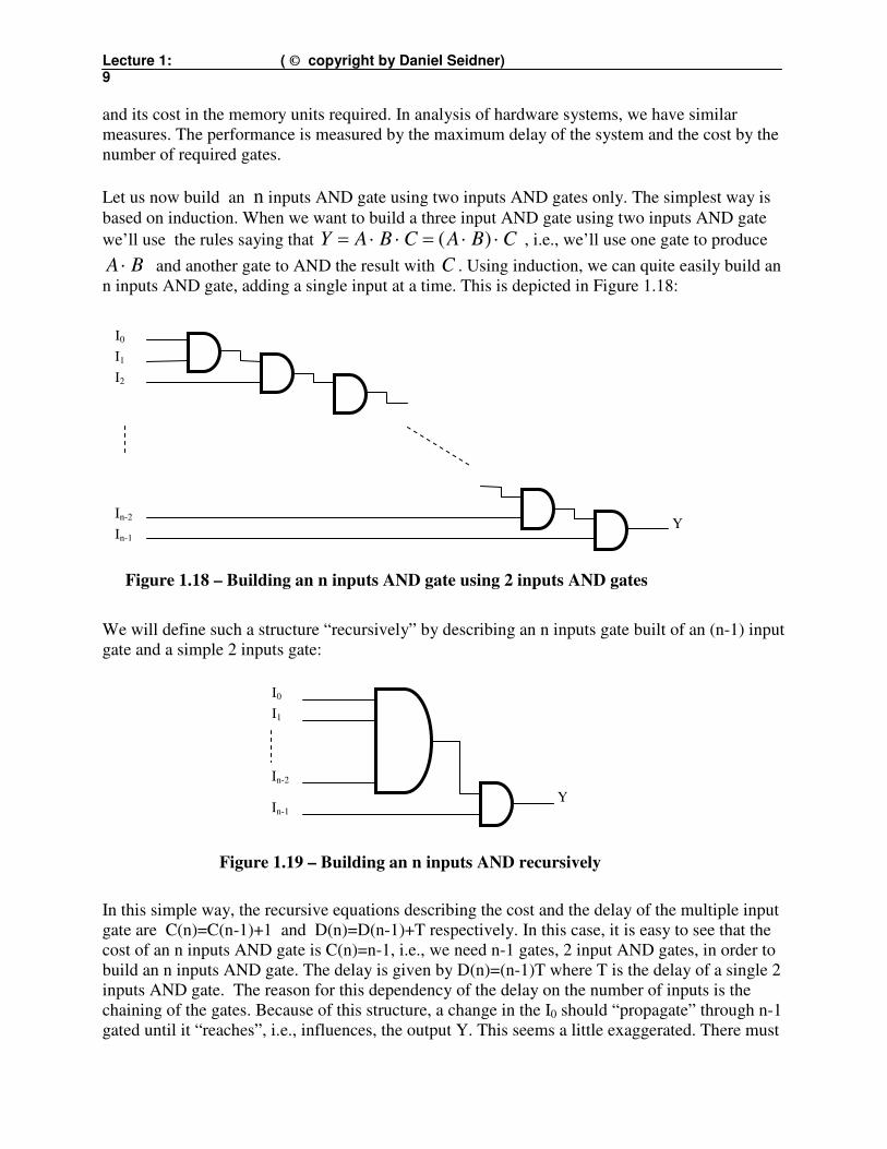
and its cost in the memory units required. In analysis of hardware systems, we have similar
measures. The performance is measured by the maximum delay of the system and the cost by the
number of required gates.
Let us now build an n inputs AND gate using two inputs AND gates only. The simplest way is
based on induction. When we want to build a three input AND gate using two inputs AND gate
we’ll use the rules saying that CBACBAY ⋅⋅=⋅⋅= )( , i.e., we’ll use one gate to produce
BA ⋅ and another gate to AND the result with C . Using induction, we can quite easily build an
n inputs AND gate, adding a single input at a time. This is depicted in Figure 1.18:
We will define such a structure “recursively” by describing an n inputs gate built of an (n-1) input
gate and a simple 2 inputs gate:
In this simple way, the recursive equations describing the cost and the delay of the multiple input
gate are C(n)=C(n-1)+1 and D(n)=D(n-1)+T respectively. In this case, it is easy to see that the
cost of an n inputs AND gate is C(n)=n-1, i.e., we need n-1 gates, 2 input AND gates, in order to
build an n inputs AND gate. The delay is given by D(n)=(n-1)T where T is the delay of a single 2
inputs AND gate. The reason for this dependency of the delay on the number of inputs is the
chaining of the gates. Because of this structure, a change in the I0 should “propagate” through n-1
gated until it “reaches”, i.e., influences, the output Y. This seems a little exaggerated. There must
Figure 1.18 – Building an n inputs AND gate using 2 inputs AND gates
I0
I1
I2
In-2
In-1
Y
Figure 1.19 – Building an n inputs AND recursively
In-1
Y
I0
I1
In-2

Lecture 1: ( © copyright by Daniel Seidner) 10
be a better way. That way is to use a binary tree structure. The depth of that tree will determine
the maximal delay. This can be seen in Figure 1.20 below.
Figure 1.20 – Building an n inputs AND gate using a tree of inputs AND gates
Y
I0
I1
I2
I3
In-4
In-3
In-2
In-1
I4
I5
I6
I7
In/2-1

Lecture 1: ( © copyright by Daniel Seidner) 11
We can define such a structure “recursively” by describing an n inputs gate built of two n/2 input
gates:
The cost of such an n inputs gate stays C(n)=n-1. This is so since it really does not matter how we
add the inputs, since every new input forces us to add a single gate. The recursive equation
describing the cost is C(n)=2C(n/2)+1 having n/2 but also a factor of 2 certifies a linear cost.
It is quite clear from Figure 1.19 that the delay follows the recursive equations
TnDnD += )2/()( . This immediately means that the delay is logarithmic, i.e.,
nTnD2
lg)( ⋅= . This is so since we can write:
TTTnDTTnDTnDnD +++=++=+= )8/()4/()2/()( , etc., so we see that we
have to sum n2
lg times the delay T.
When n is not an exact power of 2, there are several optional trees, all with depth of n2lg , to
arrange the gates. The delay in such case is given by nTnD2
lg)( ⋅= .
We use basic gates of 2 inputs although in practice gates with more inputs are available.
Note that if we had a basic gate of 3 inputs we would get nTnD3
lg)( ⋅= .
Figure 1.21 –A recursive building of an n inputs AND gate
Y
I0
I1
In/2-1
In/2
In/2+1
In-1
n/2 inputs
n/2 inputs

Lecture 1: ( © copyright by Daniel Seidner) 12
1.12 Decoders
It is time now to get to our first useful system. We are going to build a Decoder. A decoder has n
inputs and 2n outputs. Only one of its outputs is “1” at a given time. The combination of the n
input lines, each can be “0” or “1”, determines which of the outputs is “on”, i.e., “1”. As a matter
of fact, the combination at the input represents a binary number in which the rightmost digit has a
value (or weight) of 1, the next digit has a value of 2, the next has a value of 4 and the next of 8
and so on. Thus the combination 0101 has a value of 0ּ8+1ּ4+0ּ2+1ּ1=5 and the combination
0111 has a value of 7 since 0ּ8+1ּ4+1ּ2+1ּ1=7. We would like to build a decoder having only
two inputs, I0 and I1, forming together a two bit number [I1, I0] which can have the values 0,1,2 or
3. And so, the decoder has 4 outputs Y0, Y1, Y2, and Y3. We would like the i-th output to be “1”
when the input has the combination that represent the number i.
How do we do that?
We use a truth table to describe the decoder and then find the equations of the outputs from that
table;
[I1 I0] Y0 Y1 Y2 Y3
00 1 0 0 0
01 0 1 0 0
10 0 0 1 0
11 0 0 0 1
We immediately see that the equations of the outputs are given by:
010IIY ⋅=
011IIY ⋅=
012IIY ⋅=
013IIY ⋅=
So the decoder can be built as described in Figure 1.22 below:

Lecture 1: ( © copyright by Daniel Seidner) 13
Note that the procedure that we’ll always use is: First, define the required device. Then, build its
truth table. Then, find its equations from the truth table. Then implement it with gates.
We would now like to recursively build an n inputs decoder using (n-1) inputs decoders. When
we design a VLSI chip, we want to get rid of all redundant parts. Another look at Figure 1.23
reveals that the two decoders produce similar outputs. Therefore, a better design is to use a single
decoder and duplicate its output as shown in Figure 1.26.
Figure 1.22 – A 2 inputs → 4 outputs decoder
Y0
Y1
Y2
Y3
I0
I1
Figure 1.26 – A Recursive Decoder
I0 - In-2
n-1
(n-1)→2(n-1)
Decoder
Y0
Y1
Y2
Y2n-1
-1
In-1
Y2n-1
Y2n-1
+1
Y2n-1
2n-1
outputs
2n-1
outputs
2n outputs
Lecture 1: ( © copyright by Daniel Seidner) 14
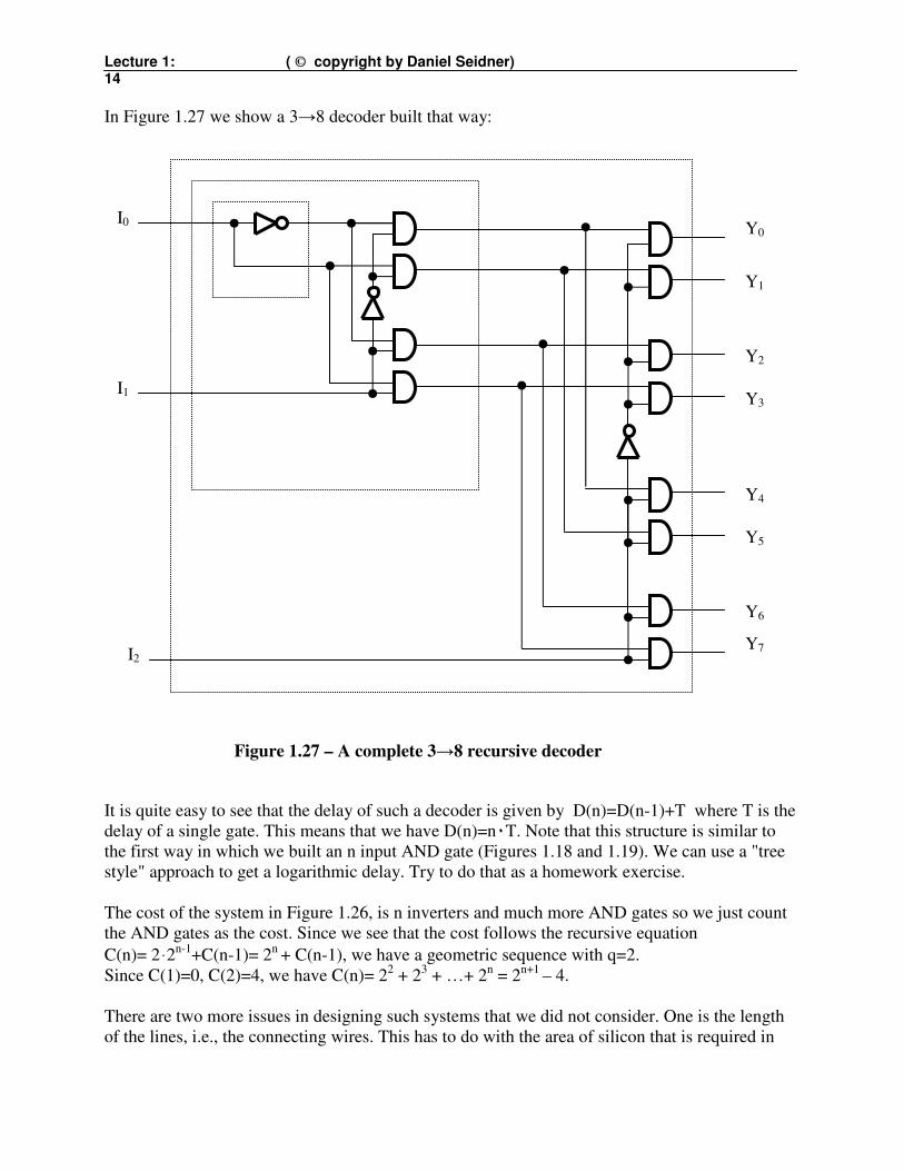
In Figure 1.27 we show a 3→8 decoder built that way:
It is quite easy to see that the delay of such a decoder is given by D(n)=D(n-1)+T where T is the
delay of a single gate. This means that we have D(n)=n٠T. Note that this structure is similar to
the first way in which we built an n input AND gate (Figures 1.18 and 1.19). We can use a "tree
style" approach to get a logarithmic delay. Try to do that as a homework exercise.
The cost of the system in Figure 1.26, is n inverters and much more AND gates so we just count
the AND gates as the cost. Since we see that the cost follows the recursive equation
C(n)= 2ּ2n-1+C(n-1)= 2
n + C(n-1), we have a geometric sequence with q=2.
Since C(1)=0, C(2)=4, we have C(n)= 22 + 2
3 + …+ 2
n = 2
n+1 – 4.
There are two more issues in designing such systems that we did not consider. One is the length
of the lines, i.e., the connecting wires. This has to do with the area of silicon that is required in
Figure 1.27 – A complete 3→8 recursive decoder
I2
I1
I0
Y0
Y7
Y1
Y2
Y3
Y4
Y5
Y6

Lecture 1: ( © copyright by Daniel Seidner) 15
order to implement the design on silicon. We will not discuss that issue. The other thing is the
Fan out of the gates. The gates are electronic devices which have output and input currents. Since
the output current of a gate is limited, it can “drive” only a limited number of gates. The number
of gate inputs that can be driven by the output of a gate is called the Fan out of that gate. A
typical value of the Fan out is 10 to 20. We would like to analyze a much severe case where the
fan out of a gate is only 2. (Less then 2 means that we can connect the output of a gate only to a
single input. This is too restrictive.)
In our decoder, we see that each AND gate drives two other gates, so there is no problem there.
However, the inverters drive up to 2n-1
inputs, i.e., the number of the inputs that should be driven
by the inverters is exponential! How can we overcome such a problem when the allowed fan out
is only two?
The answer is that we should build a “tree” of inverters to produce 2n-1
inverted outputs and 2n-1
non-inverted outputs from the In-1 input:
Note that since the depth of such a tree is about n, we almost did not increase the delay of the
decoder.
Figure 1.28 – A fan out expansion tree
In-1
In-1
In-1

Lecture 1: ( © copyright by Daniel Seidner) 16
1.13 Multiplexers
A multiplexer (Mux), as a decoder, is one of the basic devices used in building computers. An
n→m multiplexer, n>m, is a device with n inputs and m outputs. It also has some select inputs
that determine which of the inputs are transferred to the outputs.
1.13.1 A simple mux
We follow our design procedure: First, define the required device. Then, build its truth table.
Then, find its equations from the truth table. Then implement it with gates. So, we first define the
simplest multiplexer which is a 2→1 multiplexer. It has two data inputs A and B (or I0 and I1) and
a single data output, Y. It also has a single select input denoted by S. Its drawing and function is
given in Figure 1.29.
As shown in Figure 1.29b, the multiplexer functions as a switch. The S input determines which of
the two inputs is “connected” to the output Y. When S=”0”, we have Y=A (or Y=I0). When
S=”1”, we have Y=B (or Y=I1). The function of the mux can be written as:
A if S=0
Y =
B if S=1
Figure 1.29b – A 2→1 mux selects between the 2 inputs
A (or I0)
B (or I1)
Y
2→1
S
Figure 1.29a – The schematic drawing of 2→1 multiplexer
A (or I0)
B (or I1)
Y
S
0
1

Lecture 1: ( © copyright by Daniel Seidner) 17
The truth table is therefore:
S A (I0) B (I1) Y
0 0 0 0
0 0 1 0
0 1 0 1
0 1 1 1
1 0 0 0
1 0 1 1
1 1 0 0
1 1 1 1
The logic function of a mux is very simple:
SBSAY ⋅+⋅= (or if we use the other notation: SISIY ⋅+⋅=10
).
The implementation using gates is also simple:
Figure 1.30 – The inside of 2→1 multiplexer
A (or I0)
B (or I1)
Y
S
Lecture 1: ( © copyright by Daniel Seidner) 18
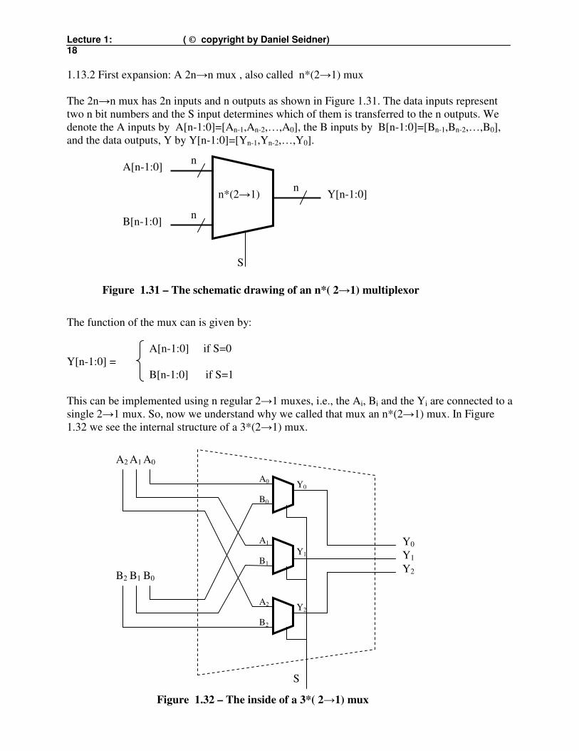
1.13.2 First expansion: A 2n→n mux , also called n*(2→1) mux
The 2n→n mux has 2n inputs and n outputs as shown in Figure 1.31. The data inputs represent
two n bit numbers and the S input determines which of them is transferred to the n outputs. We
denote the A inputs by A[n-1:0]=[An-1,An-2,…,A0], the B inputs by B[n-1:0]=[Bn-1,Bn-2,…,B0],
and the data outputs, Y by Y[n-1:0]=[Yn-1,Yn-2,…,Y0].
The function of the mux can is given by:
A[n-1:0] if S=0
Y[n-1:0] =
B[n-1:0] if S=1
This can be implemented using n regular 2→1 muxes, i.e., the Ai, Bi and the Yi are connected to a
single 2→1 mux. So, now we understand why we called that mux an n*(2→1) mux. In Figure
1.32 we see the internal structure of a 3*(2→1) mux.
A[n-1:0]
B[n-1:0]
Y[n-1:0]
n*(2→1)
Figure 1.31 – The schematic drawing of an n*( 2→1) multiplexor
S
n
n
n
Figure 1.32 – The inside of a 3*( 2→1) mux
A0
Y0
S
Y1
Y2
A1
A2
B0
B1
B2
B0
B1
B2
A0
A1
A2
Y0
Y1
Y2

Lecture 1: ( © copyright by Daniel Seidner) 19
1.13.3 Second expansion: A 2k→1 mux
The 2k→1 mux has 2
k inputs and a single output as shown in Figure 1.31. There are also k select
inputs denoted S[k-1:0]=[Sk-1,Sk-2,…,S1,S0]. There are 2k
combinations to the select lines. When
S[k-1:0]=i, i.e., the combination of [Sk-1,…,S0] represents the number i, the i-th input is
transferred to the output Y. Since there are 2k inputs we have chosen to denote those inputs by I0,
I1, …, I2k
-1. Note that the simple 2→1 mux we studied before, is a particular case with k=1.
We would like to build an 8→1 (i.e., a 23→1) mux using 2 muxes of 4→1. This is pretty easy.
We have to add another select input, S2, to the two select inputs, S1 and S0, of the 4→1 muxes
(i.e., 22→1 muxes). This S2 input will choose between the two outputs of the two 4→1 muxes, as
in Figure 1.34 below.
I0
I2k
-1
Y
2k→1
Figure 1.33 – The schematic drawing of a 2k→1 multiplexor
S[k-1:0]
I1
k
Figure 1.34 – A 23→1 mux build of two 2
2→1 muxes
Y
2→1
S2
I0
4→1
S0
I1
S1
I3
I2
I4
4→1
S0
I5
S1
I7
I6
The number
represented by
S[k-1:0] is the
serial number of
the input
transferred to the
output.
S2 S1 S0
0 0 0 = 0
0 0 1 = 1
0 1 0 = 2
0 1 1 = 3
1 0 0 = 4
1 0 1 = 5
1 1 0 = 6
1 1 1 = 7

Lecture 1: ( © copyright by Daniel Seidner) 20
Since adding a select line exactly doubles the number of combinations, we can similarly build a
2k→1 mux using two 2
k-1→1 muxes and a single 2→1 mux. Thus, we can build a 2
k→1 mux
recursively. In Figure 1.35 we see the recursive definition of such a mux.
The cost equation is C( k) = 2٠C(k-1) + C(1). This means that the cost is actually:
C(k) = C(1)٠[1+ 2+4+…+2k-1
]= C(1)٠(2k-1). Note that here we look at k instead of n where n is
the number of the inputs and follows n=2k. So C(n)=C2→1٠(n-1).
The delay equation is D( k) = D(k-1) + D(1). This means that the delay is given by D(k) = k٠D(1)
or D(n) = lg 2 n٠ D2→1.
In Figure 1.36 we show the entire tree of an 8→1 mux.
Figure 1.35 – Building a mux recursively
Y
2→1
Sk-1
k-1
Sk-2,…,S0
I0
2k-1→1
I1
I2k-1
-1
I2k-1
2k-1→1
I2k-1
+1
I2k
-1
k-1
k-1
2k-1
inputs
2k-1
inputs

Lecture 1: ( © copyright by Daniel Seidner) 21
Figure 1.36 – The entire recursion depth in an 8→1 mux
S2
I0
I1
I2
S1
S0
I4
I5
I7
I6
2→1
2→1
2→1
2→1
2→1
2→1
2→1
I3
Y

Lecture 1: ( © copyright by Daniel Seidner) 22
1.13.4 Third expansion: An n*( 2k→1) mux
The n*(2k→1) mux has 2
k inputs, n bits each, i.e., each input represent an n bits binary number,
and a single n bits output as shown in Figure 1.37. There are also k select inputs denoted
S[k-1:0]=[Sk-1,Sk-2,…,S1,S0]. There are 2k
combinations to the select lines. When S[k-1:0]=i , the
i-th input is transferred to the output Y. Since there are 2k inputs we have choose to denote those
inputs by I0, I1, …, I2k
-1, sometimes denoted A,B,…,Z.
Similarly to the first expansion, the n*(2k→1) mux is built of n muxes of 2
k→1, each of them
takes care for one of the n bits. An example of a 12→3 mux, i.e., a 3*(22→1) mux, is given in
Figure 1.38 below.
Figure 1.37 – The schematic drawing of an n*(2k→1) multiplexer
I0[n-1:0] (or A[n-1:0])
I2k
-1[n-1:0] (or Z[n-1:0])
Y[n-1:0]
n*(2k→1)
Sk-1,…,S0
I1[n-1:0] (or B[n-1:0])
k
n
n
n
n

Lecture 1: ( © copyright by Daniel Seidner) 23
We can also take apart the 4→1 muxes, which , as we already know, are built of 2→1 muxes:
Figure 1.38 – The inside of a 3*( 22→1) mux
Y0
Y1
Y2
A0
A1
A2
Y0
Y2
B0
B1
B2
C0
C1
C2
D0
D1
D2
B0
A0
D0
C0
B2
A2
D2
C2
B1
A1
D1
C1
S0
S1
Y1

Lecture 1: ( © copyright by Daniel Seidner) 24
Figure 1.40 below shows the entire muxes family:
Figure 1.39 – The inside of a 3*( 22→1) mux in detail
A0
A1
A2
Y0
Y2
B0
B1
B2
C0
C1
C2
D0
D1
D2
S1
S0
Y1
B0
A0
D0
C0
B2
A2
D2
C2
B1
A1
D1
C1
Y0
Y1
Y2

Lecture 1: ( © copyright by Daniel Seidner) 25
Figure 1.40 – The entire multiplexers family
I0
I2k
-1
Y
2k→1
S[k-1:0]
I1
k
A[n-1:0]
B[n-1:0]
Y[n-1:0]
n*(2→1)
S
n
n
n
A (or I0)
B (or I1)
Y
2→1
S
I0[n-1:0] (or A[n-1:0])
I2k
-1[n-1:0] (or Z[n-1:0])
Y[n-1:0]
n*(2k→1)
Sk-1,…,S0
I1[n-1:0] (or B[n-1:0])
k
n
n
n
n
First expansion:
N bits in parallel
2nd expansion:
binary tree for 2k
inputs
3rd expansion:
2k inputs of N bits in
parallel
duplication tree structure

Lecture 1: ( © copyright by Daniel Seidner) 26
We have only one last thing to say about muxes and decoders. They complement each other. A
mux is the “inverse” of a decoder. To show that, we will change our interpretation of decoders.
Let us look at a 2→4 decoder that has an enable input denoted E. If E=”0” all outputs of the
decoder are “0”. If E=”1”, then the output selected by the code, or combination, of the inputs is
“1”. So, one can see the decoder as a switch controlled by the inputs that transfers the E data into
one of the output as in Figure 1.41.
We can use Muxes and Decoders to multiplex multiple data streams on a single line as in Figure
1.42. This is called TDM, Time Division Multiplexing, since when we sequentially change the
selection code S[1:0]=0→1→2→3→0→1→… etc., we have a different data stream appearing on
the line at different times. Note that the rate of switching the select lines should be 4 times higher
than the rate in which the data streams may change.
Suggested homework: 1)A “recursive” comparator 2) "ALT" detector 3) A “tree” decoder
E
I0
I1
Y0
Y1
Y2
Y3
2→1
decoder
I[1:0]=[I1,I0]
Y0
Y1
Y2
Y3
E
2
≡
Figure 1.41 – A decoder as a controlled switch
Y0
Y1
Y2
Y3
E
2
I0
I1
I2
I3
Y
2
2
S1,S0
Figure 1.42 – 4 data lines sharing a single line

Lecture 1: ( © copyright by Daniel Seidner) 27
3) Adders and ALU circuits
In this section we will use the knowledge we acquired in the previous two chapters to design
Adders and ALU.
3.1) A Half Adder
We begin with designing a component called a Half Adder. This component, depicted in Figure
3.1 below, as well as its truth-table, is capable of adding two one bit numbers.
A B Co Y
0 0 0 0
0 1 0 1
1 0 0 1
1 1 1 0
The equations of a Half-Adder are easily found from its truth-tabe:
BABABAY ⊕=⋅+⋅=
BACo
⋅=
So, the implementation of a Half-Adder (HA) is simple and involves only two gates:
Figure 3.1 – A Half .א
HA
B A
Y Co
Co
II III
Figure 3.2 – The inside of a Half-Adder
IV. A

Lecture 1: ( © copyright by Daniel Seidner) 28
The reason that this device is called a Half-Adder is that we need two of these in order to add
longer numbers. Let us demonstrate it. We’ll try to build an Adder that will add two 6 bits
numbers A[5:0] and B[5:0]. We connect the Ai-th and Bi-th bits to a Half-Adder that produces the
Yi-th output and hope for good:
Let us now try to use the adder for adding some unsigned numbers. We do not have any problems
in adding A=001100 and B=010001. But we seem to have a problem adding A=001100 and B=
001010. The 4 LSBs of Y[5:0], i.e., Y0, Y1, Y2, and Y3 are OK. But Y4 is not, since the addition
of A3 and B3 produces a carry, given by the signal C4 which is “1”, but has no influence on Y4.
Such an adder cannot handle cases of carry. We need to do some modifications to this design as is
explained below.
3.2) A Full Adder
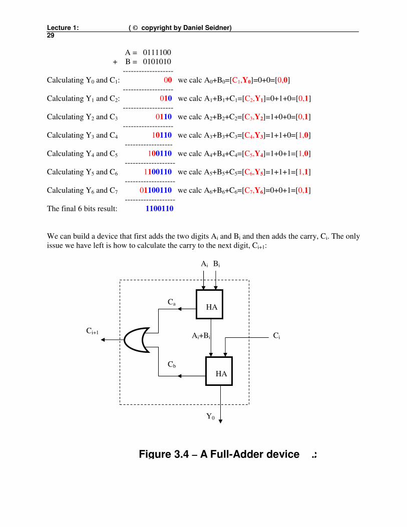
Let us try to imitate the way we, humans, do the addition of two binary numbers. Let us add the
two numbers A=0111100 and B=0101010. We add the numbers bit by bit. When carry is
produced, we add it to the next digit; (the result of each step is in red, older results are in blue)
Figure 3.3 – Trying to build an adder .ב
HA
B0 A0
Y0
C1
HA
B1 A1
Y1
C2
HA
B2 A2
Y2
C3
HA
B3 A3
Y3
C4
HA
B4 A4
Y4
C5
HA
B5 A5
Y5
C6
Lecture 1: ( © copyright by Daniel Seidner) 29
A = 0111100
+ B = 0101010
-------------------
Calculating Y0 and C1: 00 we calc A0+B0=[C1,Y0]=0+0=[0,0]
-------------------
Calculating Y1 and C2: 010 we calc A1+B1+C1=[C2,Y1]=0+1+0=[0,1]
-------------------
Calculating Y2 and C3 0110 we calc A2+B2+C2=[C3,Y2]=1+0+0=[0,1]
-------------------
Calculating Y3 and C4 10110 we calc A3+B3+C3=[C4,Y3]=1+1+0=[1,0]
------------------
Calculating Y4 and C5 100110 we calc A4+B4+C4=[C5,Y4]=1+0+1=[1,0]
-------------------
Calculating Y5 and C6 1100110 we calc A5+B5+C5=[C6,Y5]=1+1+1=[1,1]
-------------------
Calculating Y6 and C7 01100110 we calc A6+B6+C6=[C7,Y6]=0+0+1=[0,1]
-------------------
The final 6 bits result: 1100110
We can build a device that first adds the two digits Ai and Bi and then adds the carry, Ci. The only
issue we have left is how to calculate the carry to the next digit, Ci+1:
Figure 3.4 – A Full-Adder device .ג
HA
Ci Ci+1
Y0
Cb
HA
Bi Ai
Ai+Bi
Ca

Lecture 1: ( © copyright by Daniel Seidner) 30
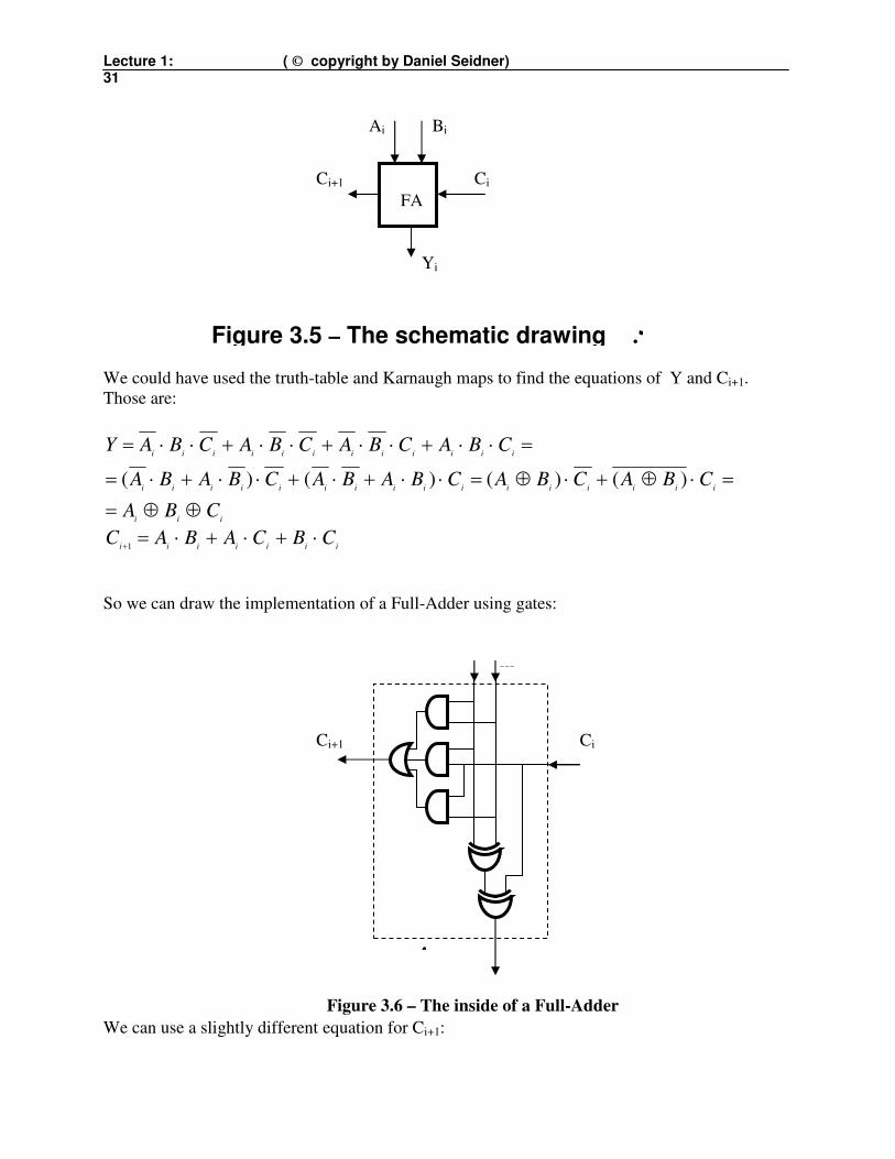
Such a device is called a Full-Adder (FA). In Figure 3.4 we demonstrate building a Full-Adder
using two Half-Adders. We see that we first add the two digits and then add also the carry in. It is
easy to see that we would have carry out only when two (or more) of the inputs Ai, Bi, Ci are “1”s
(see the truth-table below). Let us now make sure that the circuit calculates Ci+1 correctly:
When Ai=Bi=”1”, then Ca=”1”, and so Ci+1=”1”. This is the only case in which Ca=”1”.
When Ci=”0”, we have no problem since Cb=”0”, and so only Ca can cause Ci+1 to be “1”. This of
course happens only if Ai=Bi=”1”.
When Ci=”1”, we have to worry only about the case in which we have Ai≠Bi, since if they are
equal, then if they are “0”, Ai+Bi is also “0” and no carry is produced at all. If they are “1”s, then,
although Cb=”0”, we have carry since Ca=”1”.
When Ci=”1” and Ai≠Bi, we know that there must be carry. Since in this case we have
Ai+Bi=”1”, we also have Cb=”1” and therefore Ci+1=”1” as desired.
Thus, the circuit depicted in Figure 3.4 satisfies the truth-table of a Full-Adder (FA) that is shown
below.
By the way, note that the unsigned number [Ci+1,Y] actually represents the number of “1”s in the
set { Ai, Bi, Ci }.
Ci Ai Bi Ci+1 Yi
0 0 0 0 0
0 0 1 0 1
0 1 0 0 1
0 1 1 1 0
1 0 0 0 1
1 0 1 1 0
1 1 0 1 0
1 1 1 1 1
The schematic drawing of a Full-Adder is shown in Figure 3.5 below.
Lecture 1: ( © copyright by Daniel Seidner) 31
We could have used the truth-table and Karnaugh maps to find the equations of Y and Ci+1.
Those are:
iii
iiiiiiiiiiiiiiii
iiiiiiiiiiii
CBA
CBACBACBABACBABA
CBACBACBACBAY
⊕⊕=
=⋅⊕+⋅⊕=⋅⋅+⋅+⋅⋅+⋅=
=⋅⋅+⋅⋅+⋅⋅+⋅⋅=
)()()()(
iiiiiiiCBCABAC ⋅+⋅+⋅=
+1
So we can draw the implementation of a Full-Adder using gates:
We can use a slightly different equation for Ci+1:
Ci+1
III.
Ci
IV. A
Figure 3.6 – The inside of a Full-Adder
FA
Bi Ai
Yi
Ci+1 Ci
Figure 3.5 – The schematic drawing .ד

Lecture 1: ( © copyright by Daniel Seidner) 32
iiiiiiCBABAC ⋅⊕+⋅=
+)(
1
which changes the implementation slightly to:
Note that this implementation has fewer gates than the previous one, but the delay from Ai or Bi
to Ci+1 is larger since an extra gate is included in this path (if a 3 input gate has the same delay).
Note that this implementation is identical to Figure 3.4.
We are ready now to build our first Adder.
3.3) A Ripple Carry Adder
A Ripple Carry Adder is an adder built of Full-Adders very similarly to our first try of Figure 3.3.
This time we use Full-Adders instead of the Half-Adders and connect the carry-out of a digit to
the carry-in of the next digit:
Ci+1
VII.
Figure 3.7 – Another implementation of a Full-Adder
Ci
VIII. A

Lecture 1: ( © copyright by Daniel Seidner) 33
This kind of an adder is called a Ripple Carry Adder (RCA) since the carry propagates through
the Full-Adders like a wave.
Note that, as explained in the previous chapter, this adder is capable of adding two unsigned
numbers, or two 2’s Comp. numbers.
Figure 3.8 – A Ripple Carry Adder .ה
B2 A2
Y2
C3
B1 A1
Y1
C2
B0 A0
Y0
C1
Bn-1 An-1
Yn-1
Cn
Bi Ai
Yi
Ci+1 Ci Cn-1 C0
OVF
A[n-1:0] B[n-1:0]
II. Y
Adder
n
n n
Cn
III. Figure 3.9 - The schematic
C0
OVF
Lecture 1: ( © copyright by Daniel Seidner) 34
The cost of a RCA with width of n bits, i.e., an adder capable of adding two n bits numbers, is n
times the cost of a single Full-Adder. Let us choose the implementation of Figure 3.7, i.e., we
have 5 gates in a Full-Adder. Thus, we have
C(n) = n ٠ CFA = 5٠n
This means that when we double the width of our processor word we will need to pay twice the
price.
The delay of a RCA depends on the carry propagation. The first stage calculating Y0, will have
the correct result after the delay of the two XOR gates of the right-hand side FA. The second
stage, calculating Y1, will have the correct result later, since we have to wait for C1 and then wait
another delay of a XOR gate till Y1 is ready. For Y2, we have to wait for C2 which depends on C1,
and so on, as shown in Figure 3.10. Thus, a two gates delay should be added for every bit.
Eventually we have:
D(n) = n ٠ 2 ٠ T + T , where T is the delay of a single gate.
This is so since in order to calculate Cn, which is required some times, we need to wait 3T until
we produce C1 and then, 2(n-1)T until the carry propagates through the next (n-1) stages, i.e., the
total delay of this adder is (2n+1)T.
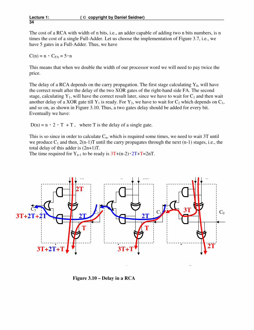
The time required for Yn-1 to be ready is 3T+(n-2)٠2T+T=2nT.
C3
Figure 3.10 – Delay in a RCA
VI.
C2
VII. A
VIII
X.
C0
XI. A
XII
XIII XIV.
C1
XV. A 2T
3T
T
3T+T
T
2T
2T
2T
3T+2T+T
3T+2T+2T
Lecture 1: ( © copyright by Daniel Seidner) 35
In case we would have used the implementation of Figure 3.6, even only for the 1st stage, we
would shorten the time by T to all outputs (except Y0), and so we would have D(n) = n ٠ 2 ٠ T ,
(for Cn).
We definitely have D(n) = O( n ), i.e., a linear delay.
This is not a good result. It means that when we double the word width of our computer, we also
double the calculation time, i.e., we make our computer two times slower than before. We will
later try to improve the performance. We would like to have a linear cost and a logarithmic delay.
This is the best we can hope for.
3.4) ALU
Although we are not satisfied with the performance of our adder (the RCA), we are now ready to
design the heart of a CPU, the Arithmetic Logic Unit (ALU). The ALU is the part of the CPU that
does all the computations.
First, we’ll improve the functionality of our adder by adding the capability of performing
subtraction.
Since, as we already know, 1++=− BABA , all we have to do in order to subtract B from A
is to invert its bits and add the inverted number to A, and also add 1. Adding 1 is very easy. We’ll
use C0 for that. This is actually the reason we used a Full-Adder in the 1st stage instead of a Half-
Adder which is slightly faster and less expensive. Having the C0 input is also useful for "add with
carry" operations.
The SUB input controls the function of the circuit. In case SUB=”0”, B is not inverted (the XOR
gate actually means that each bit of B is XORed with SUB), and C0=”0”, thus the circuit
calculates Y=A+B. In case SUB=”1”, B is inverted and C0=”1”, so the circuit calculates Y=A-B.
(Note: try to prove that when this circuit is used for unsigned numbers subtraction, the result is
negative if Cn=”0” !! I.e., Cn is definitely not equal to the borrow we expect when subtracting 2
unsigned numbers).
Lecture 1: ( © copyright by Daniel Seidner) 36
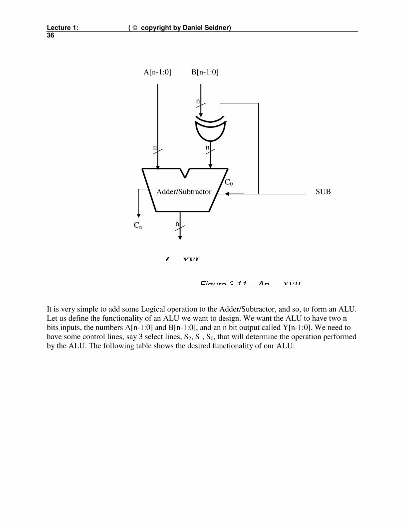
It is very simple to add some Logical operation to the Adder/Subtractor, and so, to form an ALU.
Let us define the functionality of an ALU we want to design. We want the ALU to have two n
bits inputs, the numbers A[n-1:0] and B[n-1:0], and an n bit output called Y[n-1:0]. We need to
have some control lines, say 3 select lines, S2, S1, S0, that will determine the operation performed
by the ALU. The following table shows the desired functionality of our ALU:
A[n-1:0] B[n-1:0]
XVI. Y
Adder/Subtractor
n
n n
Cn
XVII. Figure 3.11 - An
n
C0
SUB

Lecture 1: ( © copyright by Daniel Seidner) 37
S[2:0] Code
S2 S1 S0
The operation
performed by the
ALU
The name
of the
operation
0 0 0 Y= A plus B Add
0 0 1 Y= A - B Sub
0 1 0 Y= A ٠ B AND
0 1 1 Y= A + B OR
1 0 0 Y= A ⊕ B XOR
1 0 1 Y= A NOT
1 1 0 Y= A
1 1 1 Y= B
The way to get such functionality is to perform all those operations (almost) in parallel using 8
(actually 7) h/w units that perform those 8 operations. Some of the units are very simple, just n
gates each (e.g., the AND, OR, XOR, NOT, i.e., all the logical operations). Some are much more
complicated (e.g., the Adder/Subtractor). We use a multiplexer to select the appropriate output
according to the select code. Since the Adder/Subtractor is used for two operations, its output is
connected to two inputs of the multiplexer, the ones that are selected by [000] and [001].
We also add some special outputs. The ZR output is “1” if the ALU’s output is zero. The Cn is
“1” when there is a carry-out. We usually also add the NEG output which is the sign bit of Y, i.e.,
Yn-1, and the OVF output, which tells us if 2’s Comp overflow had occurred. (The last two
outputs are not shown in Figure 3.12).

Lecture 1: ( © copyright by Daniel Seidner) 38
n
n n
n n
n
n
n
n
n
n n
n
n
n
n
A[n-1:0] B[n-1:0]
Y[n-1:0] Cn
S0
S1
S2
Z
R
Mu
x
0 1 2 3 4 5 6 7
Figure 3.12 – The complete ALU
n n
n
n n n n
Sign
(Neg)
OV
F

Lecture 1: ( © copyright by Daniel Seidner) 39
3.5) A Conditional Sum Adder
The idea in a Conditional Sum Adder (CSA) is to compute the addition of A[n-1:0] and B[n-1:0],
i.e., two numbers of n bits each, by parts. By that we mean that the lower half of the numbers (lets
call it the LSB part of the numbers), A[n/2-1:0] and B[n/2-1:0] are added separately than the
upper part of the numbers (the MSB part), A[n-1:n/2] and B[n-1:n/2]. If we split the operation
into these two parts, we can use two separate adders (each adding n/2 bits numbers). That way we
do the computation faster since we do things in parallel (In both adders the carry propagates only
half of the way, at the same time). Instead of having delay of D(n), we’ll have a delay of D(n/2).
However, there is a problem. For the MSB part, we should add A[n-1:n/2] and B[n-1:n/2] and
Cn/2. But, Cn/2 is available only after D(n/2), i.e., when the LSB part calculation is finished. If we
then start the calculation of the MSB part (adding the Cn/2 takes also D(n/2)), the total calculation
time is D(n/2)+D(n/2), and no improvement had been acquired. The solution is to calculate 3
calculations in parallel: The 1st is A[n/2-1:0]+B[n/2-1:0]. The 2
nd is A[n-1:n/2]+B[n-1:n/2] and
the 3rd
is A[n-1:n/2]+B[n-1:n/2]+1. These 3 calculations last D(n/2). After this time we have the
3 results and Cn/2 as well. The result of A[n/2-1:0]+B[n/2-1:0] is Y[n/2-1:0]. We’ll use Cn/2 to
select the appropriate result of Y[n-1:n/2]. If Cn/2 is 0, we take the result of A[n-1:n/2]+B[n-1:n/2]
as Y[n-1:n/2]. If Cn/2 is 1, we take the result of A[n-1:n/2]+B[n-1:n/2]+1 as Y[n-1:n/2]. This is
done by adding a Mux as depicted in Figure 3.13 below. This is actually a recursive way of
building a CSA.
XVIII. Figure 3.13 - Building a CSA
A[n-1:n/2]
B[n-1:n/2]
XIX. Y
Adder
1
Cn_0
C0
A[n/2-1:0]
B[n/2-1:0]
XX. Y
Adder
n/2
n/2
Cn/2
XXI. Y
Adder
Cn_1
“0” “1”
XXII. Y
2→1 Mux n/2*(2→1) Mux
Cn
0 0 1
n/2 n/2
n/2 n/2 n/2 n/2 n/2
n/2

Lecture 1: ( © copyright by Daniel Seidner) 40
The delay is given by the recursive equation D(n) = D(n/2) +Tmux. This means that the delay is
logarithmic: D(n) = Tmux ּ lg n. This is so since whenever we double the inputs we add a delay
of a mux.
Figure 3.14 describes the entire recursion depth of a 4 bits CSA. The basic parts used are Full-
Adders and Muxes.
Since we have lg n recursive stages, where in each , the number of Full-adders is tripled, we
should have about 3lg n
= nlg 3
= n1.58
Full-Adders in a CSA of n inputs. A similar count, reversing
the order, i.e., about (n/2) Muxes at the last stage (not including the carry muxes), 3ּ(n/4) Muxes
at the one before, 32ּ(n/8) Muxes before etc., which sums up to about n
1.58 Muxes:
(n/2) + (3/2)ּ(n/2) +(3/2)2ּ(n/2)+…=(n/2)ּ[1+(3/2)
2+(3/2)
3+…+(3/2)
lg n -1] = n [ּ (3/2)
lg n-1]= 3
lg n
- n = n
lg 3 - n = n
1.58 - n ≈ n
1.58
The carry muxes, 1 for the last stage + 3 for the one before the last + 32
+…+ 3lg n -1
=
= (3lg n
- 1)/2 = (nlg 3
- 1)/2 ≈ n1.58
/2
Figure 3.14 – The entire recursion in a 4 bits CSA .ו
0 1
B0 A0
Y0
C1 C0
Y1_1
Y1
1
B1 A1
Y1_
C2
0
0
1 0 1 0 1
B2 A2
Y2_0
0
Y3_0
1
B3 A3
C4_0
0
0
1 0 1 0 1
Y2_1
C1 1
Y1_1
Y3_1
1
Y1_
C4_1
0
0
1 0 1
0 1 0 1
Y0 Y1 C4 Y2 Y3
1 0 C2 C2

Lecture 1: ( © copyright by Daniel Seidner) 41
Thus, the cost of such an adder is polynomial, C(n) = O(n1.58
). This is not a good result. We
employ such a design when we need to build a fast adder using already existing smaller adders.
The next adder we’ll discuss has a logarithmic delay and a linear cost.
3.6) A Carry Look Ahead Adder
Let us try to calculate the carry of all the stages in a logarithmic time. We notice that there are
two reasons for having a carry out from the i-th stage of an adder, i.e, from adding Ai, Bi and Ci.
(This addition produces a two bits number [Ci+1,Yi]). The carry Ci+1 can be generated in the i-th
stage or generated in a lower stage and propagate into Ci+1 (through Ci). Carry is generated only
when Ai=Bi=1. Ci will propagate through the i-th stage only if Ai≠Bi. If this is the case, we have
Ci+1=Ci. Carry will not be generated or propagated when Ai=Bi=0. So we can write the carry
equation as:
iiiiii
CBABAC ⋅⊕+⋅=+
)(1
We denote the AND of Ai and Bi by Gi which stands for generate. We denote the XOR of Ai and
Bi by Pi which stands for propagate. So we have a new equation for the relation of Ci and Ci+1:
Ci+1 = Gi + Pi ּ Ci
Note that since Gi and Pi depend only on Ai and Bi, we can calculate all of them in parallel at the
same time. Let us build a device, very similar to a Full-Adder, that calculates Yi, Gi and Pi
(instead of Yi and Ci+1 calculated by a Full-Adder). Such a device is depicted in Figure 3.15
below.
Gi
IV.
Figure 3.15 – Y and G,P calculation
Ci
V. A
Pi

Lecture 1: ( © copyright by Daniel Seidner) 42
Let us now build an adder using this device.
Let us calculate the delay of such an adder. First, the Gi-s and Pi-s are all calculated in parallel
(see the red lines in Figure 3.16). This takes T seconds, where T is the delay of a single gate.
Then, we have to wait till the dotted box calculates all the Ci-s. Let’s denote this time as TLA.
Following this, all the outputs become valid after an additional delay of a single gate (see the blue
lines in Figure 3.16). So the delay of this adder is Ttotal = 2T + TLA.
At a first glance, it seems that we earned nothing in this new design of an adder. We calculated C1
using the equation which gave: C1=G0+P0ּC0. We calculated C2 similarly by C2=G1+P1ּC1 and
C3 by C3=G2+P2ּC2. As we see from Figure 3.16, this means that we connected the circuit in
series. The delay from the minute all the Gi-s and Pi-s and C0 are ready till the time where all the
Ci-s are valid, is the delay of two gates multiplied by the number of bits in the adder, i.e.,
TLA=2nT. Thus the total delay of that adder is Ttotal = 2T + TLA=(2n+2)T. (Actually Ttotal =
(2n+1)T since Cn is calculated in parallel to Yn-1). Again we reached a situation where the delay
of the adder is linear.
So, we should try to improve the performance of the dotted box. This box is called a Carry Look
Ahead (CLA) circuit and this is the reason for calling this adder a CLA adder. We can easily see
that it is possible to calculate the carry with a logarithmic delay:
We start with calculating C1 which is given by C1=G0+P0ּC0.
A0 B0
P0
G0
C0
Y0
A1 B1
P1
G1
C1
Y1
A2 B2
P2
G2
C2
Y2
C3 C0 C1 C2
Figure 3.16 – A Carry Look Ahead Adder
Lecture 1: ( © copyright by Daniel Seidner) 43
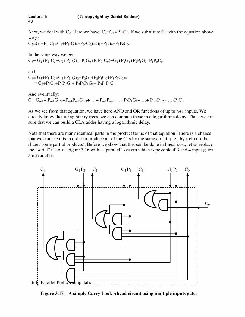
Next, we deal with C2. Here we have C2=G1+P1ּC1. If we substitute C1 with the equation above,
we get:
C2=G1+P1ּC1=G1+P1ּ(G0+P0ּC0)=G1+P1G0+P1P0C0.
In the same way we get:
C3= G2+P2ּC2=G2+P2ּ(G1+P1G0+P1P0ּC0)=G2+P2G1+P2P1G0+P1P0C0
and:
C4= G3+P3ּC3=G3+P3ּ(G2+P2G1+P2P1G0+P1P0C0)=
= G3+P3G2+P3P2G1+ P3P2P1G0+ P3P1P0C0
And eventually:
Cn=Gn-1+ Pn-1Gn-2+Pn-1Pn-2Gn-3+ …+ Pn-1Pn-2 ּ …ּP2P1G0+ …+ Pn-1Pn-2 ּ …ּP0C0
As we see from that equation, we have here AND and OR functions of up to n+1 inputs. We
already know that using binary trees, we can compute those in a logarithmic delay. Thus, we are
sure that we can build a CLA adder having a logarithmic delay.
Note that there are many identical parts in the product terms of that equation. There is a chance
that we can use this in order to produce all of the Ci-s by the same circuit (i.e., by a circuit that
shares some partial products). Before we show that this can be done in linear cost, let us replace
the “serial” CLA of Figure 3.16 with a “parallel” system which is possible if 3 and 4 input gates
are available.
3.6.1) Parallel Prefix Computation
P0 G0
C0
C1 C3
Figure 3.17 – A simple Carry Look Ahead circuit using multiple inputs gates
C0 P1 G1 C2 G2 P2

Lecture 1: ( © copyright by Daniel Seidner) 44
The algorithm enabling calculation of all of the carry outputs simultaneously, in a linear cost and
a logarithmic delay, is called Parallel Prefix Computation (PPC).
We denote the unsigned number [Gi-1, Pi-1] as σi. Actually σi equals the sum of Ai-1 and Bi-1 and
also equals to 2Gi-1+Pi-1 . (and σ0= 2C0).
We define the operation ⊗ as follows:
0 if σa=0
Πa= σa ⊗ σb = σb if σa=1
2 if σa=2
This operation helps us to detect whether the i-th stage has carry in its input. Let us look at σ3. If
it is 2, we definitely have carry at the input of the 3rd
stage, i.e., C3=1. This is so since G2=1 (i.e.,
carry is generated in the 2nd stage). If σ3=0, we are sure that there is no carry, i.e., C3=0, since
G2=P2=0 (no generation or propagation of carry in the 2nd stage). If σ3=1, we do not know if we
have carry or not. We know that P2=1, i.e., carry will propagate through the 2nd stage. So we
should look at σ2. If σ2=2, we have carry. If σ2=0, we do not have carry. If σ2=1, we must check
σ1. and so on. We therefore conclude that in order to determine Ci, the carry into the the i-th
stage, we should actually look at Πi, where Πi is defined by:
Πi = σi ⊗σi-1 ⊗σi-2 ⊗… ⊗σ2 ⊗σ1 ⊗σ0
Since σ0 equals 0 or 2, all of the Πi-s have values of 0 or 2. None of them can be equal to 1.
Eventually, when converting back from Πi to Ci the rule is therefore Ci=”1” if Πi=2.
Note that the operation ⊗ is associative:
(σa⊗σb)⊗σc = σa ⊗ (σb⊗σc)
This means that the order of computation does not matter. Note that the order of a, b, c matters,
i.e., σa⊗σb⊗σc ≠ σa ⊗σc⊗σb !!! (e.g., 2 = 1⊗2⊗0 ≠ 1⊗0⊗2 = 0).
The operation ⊗ is not commutative.
The associativity of the operation ⊗ is easily proved by checking all of the possible cases.

Lecture 1: ( © copyright by Daniel Seidner) 45
Since this is so, we can calculate Πn-1 using pairs of σ-s:
Πn-1 = σn-1 ⊗ σn-2
⊗ σn-3
⊗ σn-4
⊗ … ⊗ σ3
⊗ σ2 ⊗ σ1
⊗ σ0 =
= (σn-1 ⊗ σn-2
)⊗ (σn-3
⊗ σn-4
)⊗ … ⊗ (σ3
⊗ σ2 )⊗ (σ1
⊗ σ0)
Let us denote σ’i/2 = (σi+1
⊗ σi
). So now we have:
Πn-1 = σ’n/2-1 ⊗ σ’n/2-2
⊗ σ’n/2-3
⊗ … ⊗ σ’2
⊗ σ’1 ⊗ σ’0
The following circuit uses the associativity to produce all Πi-s from the σi-s recursively:
This circuit calculates the right results since we can see that
Π0 = σ0
Π1 = σ’0 = σ1
⊗ σ0
Π2 = σ2 ⊗ Π1
= σ2
⊗ σ1 ⊗ σ0
Π3 = σ’1 ⊗ σ’0
= (σ3
⊗σ2
)⊗ (σ1
⊗ σ0) = σ3 ⊗σ2
⊗σ1 ⊗σ0
PPC(n/2)
Πn-1 Πn-2 Πn-3
σn-1
Π5 Π4 Π3 Π2 Π1 Π0
σn-2 σ5 σ4 σ3 σ2 σ1 σ0 σ6
σ'0 σ'1 σ'2 σ'n/2-1
Figure 3.18 – Recursive PPC: PPC(n) built of PPC(n/2)
Π’0 Π’1 Π’2 Π’n/2-1

Lecture 1: ( © copyright by Daniel Seidner) 46
etc., and that we can also use the relation: Πi = σi ⊗ Πi-1.
We immediately see that the delay follows the equation: D(n)= 2T + D(n/2) where T is the delay
of the device performing the operation ⊗ . Thus, we conclude that the delay is logarithmic: D(n)
≈ 2ּTּlg n.
We also see that adding n/2 inputs caused addition of (n-1) devices which is about twice of the
number of inputs we add. This means that the cost is given by C(n) ≈ 2n. This is so since C(n) ≈ n + C(n/2) = 2(n/2)+C(n/2) ≈ 2(n/2) + 2(n/4) + C(n/4) ≈
≈ 2[ (n/2) + (n/4) + (n/8) + … + 2 + 1] = 2(n-1) ≈ 2n.
[ The exact results are: D(n)= (2ּlg n-1)T and C(n)=2n-2-lg(n) ]
Thus, the PPC version of the carry look ahead has a logarithmic delay and a linear cost.
Calculating the Ci-s from the Πi-s is easy:
Ci=”0” if Πi=0, and Ci=”1” if Πi=2. As mentioned above, Πi can never be 1, since σ0 can be 0
or 2. (I.e., if we have Πi=1, we “look” to the right and get the value of 0 or 2 from Πi-1. Even if
we get 1 and therefore should continue looking further to the right, eventually we reach σ0, that
by definition can be only 0 or 2).
Lecture 1: ( © copyright by Daniel Seidner) 47
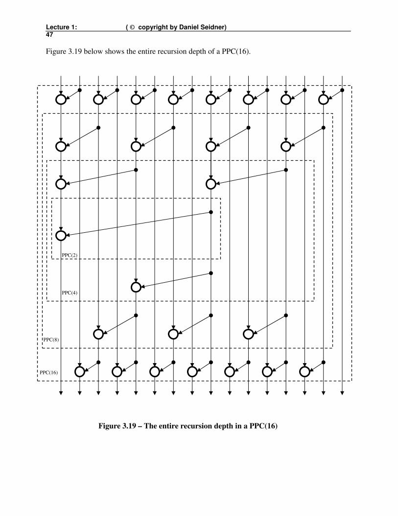
Figure 3.19 below shows the entire recursion depth of a PPC(16).
Figure 3.19 – The entire recursion depth in a PPC(16)
PPC(2)
PPC(4)
PPC(8)
PPC(16)

Lecture 1: ( © copyright by Daniel Seidner) 48
The implementation of the ⊗operation is depicted in Figure 3.20 below.
Let us verify the correctness of the implementation:
• When σ1=2 (i.e., G1=1), we have Π1=2 (i.e., G=1) as desired. (Note that in this case P1
must be 0 so P is also 0).
• When σ1=0 (i.e., G1=P1=0), we have Π1=0 as desired.
• When σ1=1 (i.e., G1=0, P1=1), we have Π1= σ0 as required (since in this case we have
G=G0 and P=P0).
Π1 = [G,P]
σ0 = [G0,P0]
≡
G1 P1 G0 P0
G P
σ1 = [G1,P1]
Figure 3.20 – The implementation of the ⊗ operation