Learn digital systems through lectures, labs and a • Gain...
20
Welcome to 6.111! • Introductions, course mechanics • Course overview • Digital signaling • Combinational logic Lecture 1 1 6.111 Fall 2019 Lecture material: Prof Anantha Chandrakasan and Dr. Chris Terman. Handouts • lecture slides, • LPset #1, • info form 6.111 Introductory Digital Systems Lab • Learn digital systems through lectures, labs and a final project using FPGAs and Verilog. • Gain experience with hands on course with real hardware – nothing in the cloud. • 6.111 satisfies – Course 6: DLAB2, II, EECS, AUS2 – Course 16: Laboratory requirement, Professional Area subject Lecture 1 6.111 Fall 2019 2 Introductions Lecture 1 6.111 Fall 2019 3 Gim Hom Lectures Diana Wofk TA LA’s Sarah Flanagan TA Mike Wang TA Joe Steinmeyer Lectures Mark Theng Isabelle Liu Sam Cherna Lydia Sun August Trollback 38-600 Lecture 1 6.111 Fall 2019 4 49 Stations Lab hours: S 1-11:45p M-R 9-11:45p F 9-5p Stata 38-644 GH Conference room
Transcript of Learn digital systems through lectures, labs and a • Gain...

Welcome to 6.111!• Introductions, course mechanics• Course overview• Digital signaling• Combinational logic
Lecture 1 16.111 Fall 2019
Lecture material: Prof Anantha Chandrakasan and Dr. Chris Terman.
Handouts• lecture slides, • LPset #1, • info form
6.111 Introductory Digital Systems Lab
• Learn digital systems through lectures, labs and a final project using FPGAs and Verilog.
• Gain experience with hands on course with real hardware – nothing in the cloud.
• 6.111 satisfies– Course 6: DLAB2, II, EECS, AUS2– Course 16: Laboratory requirement, Professional Area
subject
Lecture 1 6.111 Fall 2019 2
Introductions
Lecture 1 6.111 Fall 2019 3
Gim HomLectures
Diana WofkTA
LA’s
Sarah FlanaganTA
Mike WangTA
Joe SteinmeyerLectures
Mark ThengIsabelle LiuSam Cherna Lydia Sun August Trollback
38-600
Lecture 1 6.111 Fall 2019 4
49 Stations
Lab hours: S 1-11:45pM-R 9-11:45pF 9-5pStata
38-644GH
Conference room
Course Website: web.mit.edu/6.111
Lecture 1 6.111 Fall 2019 5
Announcements, updates, etc
Online copies of lecture notes, lpsets and labs
Final project info
On‐line grades
PDF submissions
Verilog submissions
Tools
On‐line Q&A
Policies and important dates
Lab: 38-600
Technical information and data sheet
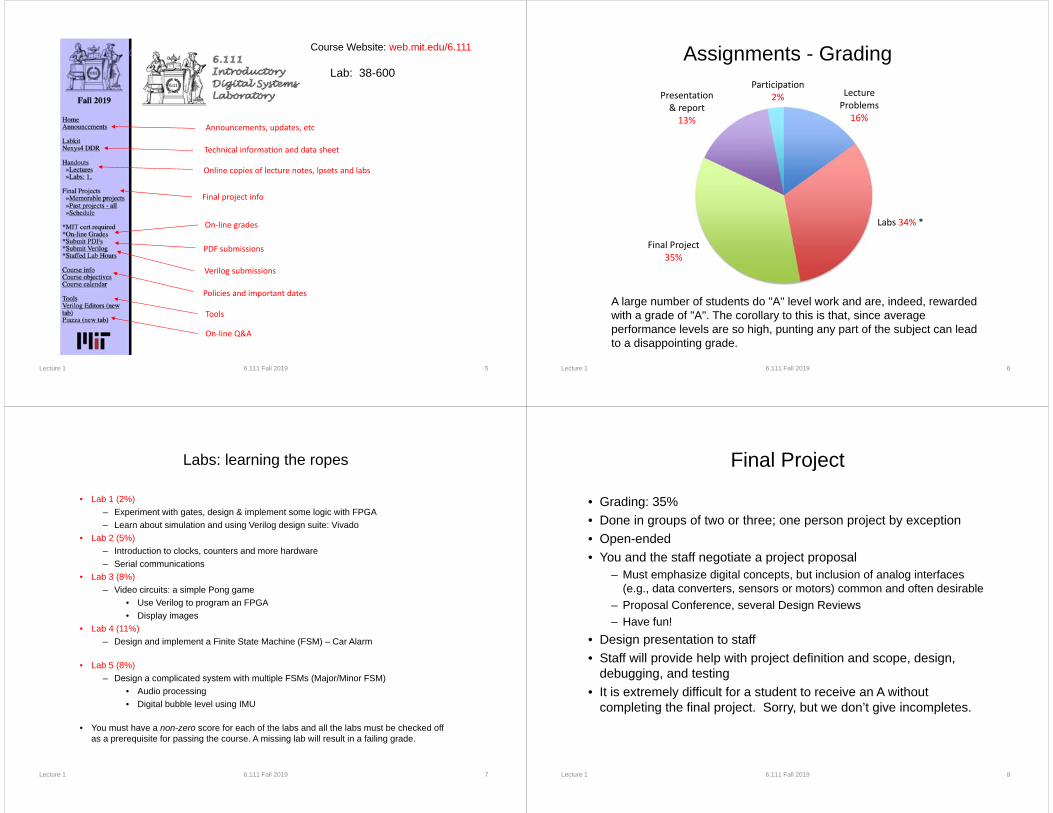
Assignments - Grading
Lecture 1 6.111 Fall 2019 6
A large number of students do "A" level work and are, indeed, rewarded with a grade of "A". The corollary to this is that, since average performance levels are so high, punting any part of the subject can lead to a disappointing grade.
Lecture Problems
16%
Labs 34% *
Final Project 35%
Presentation& report13%
Participation 2%
Labs: learning the ropes
• Lab 1 (2%)– Experiment with gates, design & implement some logic with FPGA– Learn about simulation and using Verilog design suite: Vivado
• Lab 2 (5%)– Introduction to clocks, counters and more hardware– Serial communications
• Lab 3 (8%)– Video circuits: a simple Pong game
• Use Verilog to program an FPGA• Display images
• Lab 4 (11%)– Design and implement a Finite State Machine (FSM) – Car Alarm
• Lab 5 (8%)– Design a complicated system with multiple FSMs (Major/Minor FSM)
• Audio processing • Digital bubble level using IMU
• You must have a non-zero score for each of the labs and all the labs must be checked off as a prerequisite for passing the course. A missing lab will result in a failing grade.
Lecture 1 6.111 Fall 2019 7
Final Project
• Grading: 35%• Done in groups of two or three; one person project by exception• Open-ended• You and the staff negotiate a project proposal
– Must emphasize digital concepts, but inclusion of analog interfaces (e.g., data converters, sensors or motors) common and often desirable
– Proposal Conference, several Design Reviews– Have fun!
• Design presentation to staff• Staff will provide help with project definition and scope, design,
debugging, and testing• It is extremely difficult for a student to receive an A without
completing the final project. Sorry, but we don’t give incompletes.
Lecture 1 6.111 Fall 2019 8
Project Presentation & Report (13%)
• Design proposal (2%)
• Design presentation (6%)
• Final Report (5%)
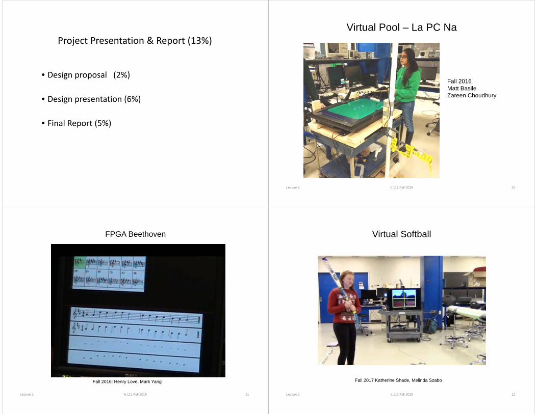
Virtual Pool – La PC Na
Lecture 1 6.111 Fall 2019 10
Fall 2016Matt BasileZareen Choudhury
FPGA Beethoven
Lecture 1 6.111 Fall 2019 11
Fall 2016: Henry Love, Mark Yang
Virtual Softball
Lecture 1 6.111 Fall 2019 12
Fall 2017 Katherine Shade, Melinda Szabo
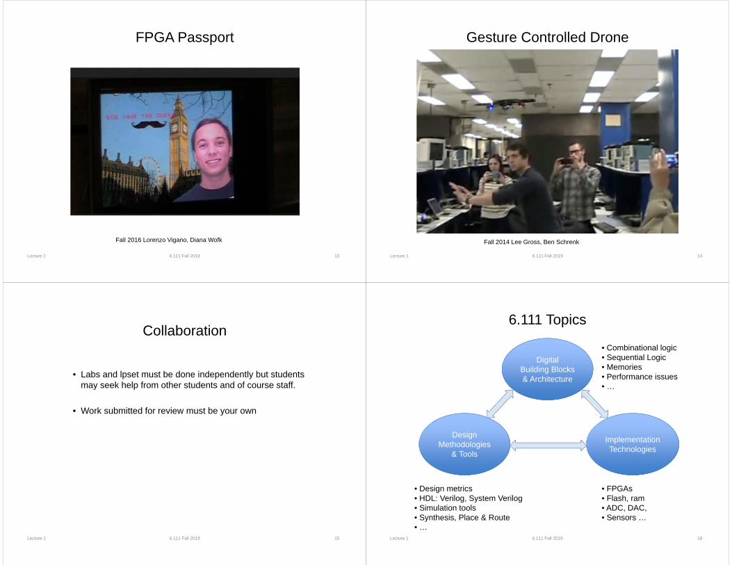
FPGA Passport
Lecture 1 6.111 Fall 2019 13
Fall 2016 Lorenzo Vigano, Diana Wofk
Gesture Controlled Drone
Lecture 1 6.111 Fall 2019 14
Fall 2014 Lee Gross, Ben Schrenk
• Labs and lpset must be done independently but students may seek help from other students and of course staff.
• Work submitted for review must be your own
Lecture 1 6.111 Fall 2019 15
Collaboration6.111 Topics
Lecture 1 6.111 Fall 2019 16
DigitalBuilding Blocks& Architecture
DesignMethodologies
& Tools
ImplementationTechnologies
• Combinational logic• Sequential Logic• Memories• Performance issues• …
• FPGAs• Flash, ram• ADC, DAC,• Sensors …
• Design metrics• HDL: Verilog, System Verilog• Simulation tools• Synthesis, Place & Route• …

Boolean Algebra
• 1854: George Boole shows that logic is math, not just philosophy!
• Boolean algebra: the mathematics of binary values
00 0
01 0
10 0
11 1
0 1
1 0
AND OR NOT
00 0
01 1
10 1
11 1
Lecture 1 6.111 Fall 2019 17
Digital Electronics
Key Link Between Logic and Circuits
• Despite existence of relays and introduction of vacuum tube in 1906, digital electronics did not emerge for thirty years!
• Claude Shannon notices similarities between Boolean algebra and electronic telephone switches
• Shannon’s 1937 MIT Master’s Thesis introduces the world to binary digital electronics
01 0
10 1
+
Lee de Forest, 1906
(The Vacuum Tube)
Lecture 1 6.111 Fall 2019 18
Evolution of Digital Electronics
UNIVAC, 1951
1900 adds/sec
IBM System/360, 1964
500,000 adds/sec
Vacuum Tubes Transistors VLSI Circuits
Intel Cascade Lake 2018 - 22 Cores >>7 Billion 14nm
First TransistorBell Labs, 1948ENIAC, 1946 4004, 1971
Digital Systems Thru the Ages
Lecture 1 6.111 Fall 2019 20
IBM 1401 Computer Circa 1962
DEC PDP 11Circa 1980
Vacuum tube computerCirca 1950

6.111 Thru the Ages
Lecture 1 6.111 Fall 2019 21
Lab kit 1990 aka “digital death” Labkit 2005
Nexys 4 - 2016 PYNQ - 2019
6.111 Evolution
6.111 Fall 2016 6.111 Fall 2019 22
Fall 2019Fall 1969
Introduces digital systems with lectures and labs on logic, flip flops, FPGAs, counters, timing, synchronization, and finite-state machines. Includes overview of accelerometers, gyros, time of light and other modern sensors. Prepares students for the design and implementation of a final project of their choice: games, music, digital filters, wireless communications, video, or graphics. Extensive use of Verilog for describing and implementing digital logic designs.
The trouble with analog signaling
Lecture 1 6.111 Fall 2019 23
The real world is full of continuous-time continuous-value (aka “analog”) signals created by physical processes: sound vibrations, light fields, voltages and currents, phase and amplitudes, …
But if we build processing elements to manipulate these signals we must use non-ideal components in real-world environments, so some amount of error (aka “noise”) is introduced. The error comes from component tolerances, electrical phenomenon (e.g., IR and LdI/dt effects), transmission losses, thermal noise, etc. Facts of life that can’t be avoided…
And the more analog processing we do, the worse it gets: signaling errors accumulate in analog systems since we can’t tell from looking at signal which wiggles were there to begin with and which got added during processing.
ProcessingElement
Music at MIT circa 1970s
Lecture 1 6.111 Fall 2019 24
Need an architecture that is noise tolerant, inexpensive, reproducible.

Solution: go digital!
Continuous valuesContinuous time
Discrete valuesDiscrete time
Lecture 1 6.111 Fall 2019 25
So we can detect small changes and restore original values
So we don’t look while it’s changing
The Digital Abstraction
Lecture 1 6.111 Fall 2019 26
RealAnalog World
“Ideal”Digital World
Volts orElectrons orErgs or Gallons
Bits
0/1
Noise
ManufacturingVariations
Keep in mind that the world is not digital, we would simply like to engineer it to behave that way. Furthermore, we must use real physical phenomena to implement digital designs!
Noise and inaccuracy are inevitable; we can’t reliably engineer perfect components – we must design our system to tolerate some amount of error if it is to process information reliably.
Digital Encoding
To ensure we can distinguish signal from noise, we’ll encode information using a fixed set of discrete values. Options are:
voltages phasecurrents frequency
Lecture 1 6.111 Fall 2019 27
For 6.111, we’ll use voltages to encode information. Current, phase and frequency encoding have uses in other applications.
Why voltage?easily generated, well understoodhistorically used, lots of circuitswith CMOS, almost zero power in steady state
No free lunch:noise sensitivity, non-ideal wires (RC time constant),
Digital processing elements
Lecture 1 6.111 Fall 2019 28
Digital processing elements restore noisy input values to legal output values – signaling errors don’t accumulate in digital systems. So the number of processing elements isn’t limited by noise problems!
The “trick” is that we’ve defined our signaling convention so that we can tell from looking at a signal which wiggles were there to begin with and which got added during processing.
We’ll keep things simple by designing our processing elements to use voltages to encode binary values (0 or 1).
ProcessingElement
-N +N
“D”
-N +N
“D”
IN
OUT

Using voltages to encode binary values
OUTPUTS:
INPUTS: Forbidden Zone
volts0 VDDVOL
0OUT 1OUT
VOH
volts0 VDDVIL
0IN 1IN
VIHVOL VOH
Noise Margins
To avoid hard-to-make decisions at the boundaries between voltages, insert a “forbidden zone” between levels. To ensure robust operation we’d like to make the noise margins as large as possible.
Lecture 1 6.111 Fall 2019 29
Forbidden Zone
Digital Signaling Specification
Digital input: VIN < VIL or VIN > VIH
Digital output: VOUT < VOL or VOUT > VOH
Noise margins: VIL−VOL and VOH −VIH
Where VOL, VIL, VIH and VOH are part of the specification for a particular family of digital components.
Now that we have a way of encoding information as a signal, we can define what it means to be digital device.
Lecture 1 6.111 Fall 2019 30
Sample DC (signaling) Specification
Source: Xilinx Virtex 5 Datasheet
Lecture 1 6.111 Fall 2019 31
Arduino Processor DC Specification
Source: ATmega328P Datasheet
Lecture 1 6.111 Fall 2019 32

A Digital Processing Element
Staticdiscipline
Output “1” if at least 2 out of 3 of
my inputs are a “1”.Otherwise, output “0”.
I will generate a validoutput in no more than
2 minutes after seeing valid inputs
input A
input B
input C
output Y
A combinational device is a processing element that has– one or more digital inputs– one or more digital outputs– a functional specification that details the value of each
output for every possible combination of valid input values
– a timing specification consisting (at minimum) of an upper bound tpd on the required time for the device to compute the specified output values from an arbitrary set of stable, valid input values
Lecture 1 6.111 Fall 2019 33
One of two discrete values
Why have processing blocks?
• The goal of modular design:
ABSTRACTION
• What does that mean anyway:– Rules simple enough for a 6-3 to follow…– Understanding BEHAVIOR without knowing IMPLEMENTATION– Predictable composition of functions– Tinker-toy assembly– Guaranteed behavior under REAL WORLD
circumstances
Lecture 1 6.111 Fall 2019 34
A Combinational Digital System
• A set of interconnected elements is a combinational device if– each circuit element is a combinational device– every input is connected to exactly one output or a constant (e.g., some
vast supply of 0’s and 1’s)– the circuit contains no directed cycles
• Why is this true?– Given an acyclic circuit meeting the above constraints, we can derive
functional and timing specs for the input/output behavior from the specs of its components!
– We’ll see lots of examples soon. But first, we need to build some combinational devices to work with…
Lecture 1 6.111 Fall 2019 35
Example Device: An Inverter
0 1 1
Static Discipline requires that we avoid the shaded regions (aka “forbidden zones”), which correspond to valid inputs but invalid outputs. Net result: combinational devices must have GAIN > 1 and be NONLINEAR.
Voltage Transfer Characteristic:Plot of VOUT vs. VIN where eachmeasurement is taken after anytransients have died out.
VOUT
VIN
VOL
VOH
VIL VIH
+-VIN VOUT 0
Note: VTC does not tell you anything about how fast a device is—it measures static behavior not dynamic behavior
IN
OUT
VV
Lecture 1 6.111 Fall 2019 36

Combinational Device Wish List
Design our system to tolerate some amount of error Add positive noise margins VTC: gain>1 & nonlinearity
Lots of gain big noise margin Cheap, small Changing voltages will require us to
dissipate power, but if no voltages are changing, we’d like zero power dissipation
Want to build devices with useful functionality (what sort of operations do we want to perform?)VOL
VIL VIH
VOH
VIN
VOUTVIN
VOUT
Lecture 1 6.111 Fall 2019 37
Wishes Granted: CMOS
VIN VOUT
Vin
Vout
VOL
VIL VIH
VOH
VIN VIL VOUT VOH
L H
VIN VIH
H L
VOUT VOL
VOUT eventually reaches VDD
VOUT eventually reaches GND
Lecture 1 6.111 Fall 2019 38
MOSFETS: Gain & Non-linearity
W
L
gate
drain
source
bulk
Inter-layer SiO2 insulation
Polysilicon wire
Doped (p-type or n-type) silicon substrate
Very thin (<20Å) high-quality SiO2insulating layer isolates gate from channel region.
Heavily doped (n-type or p-type) diffusions
Channel region: electric field from charges on gate locally “inverts” type of substrate to create a conducting channel between source and drain.
MOSFETs (metal-oxide-semiconductor field-effect transistors) are four-terminal voltage-controlled switches. Current flows between the diffusion terminals if the voltage on the gate terminal is large enough to create a conducting “channel”, otherwise the mosfet is off and the diffusion terminals are not connected.
Lecture 1 6.111 Fall 2019 39
Digital Integrated Circuits
Metal 2
M1/M2 via
Metal 1
Polysilicon
Diffusion
Mosfet (under polysilicon gate)
IBM photomicrograph (SiO2 has been removed!)
Lecture 1 6.111 Fall 2019 40
Moore’s Forever?
Lecture 1 6.111 Fall 2019 41Economist March 12-18, 2016
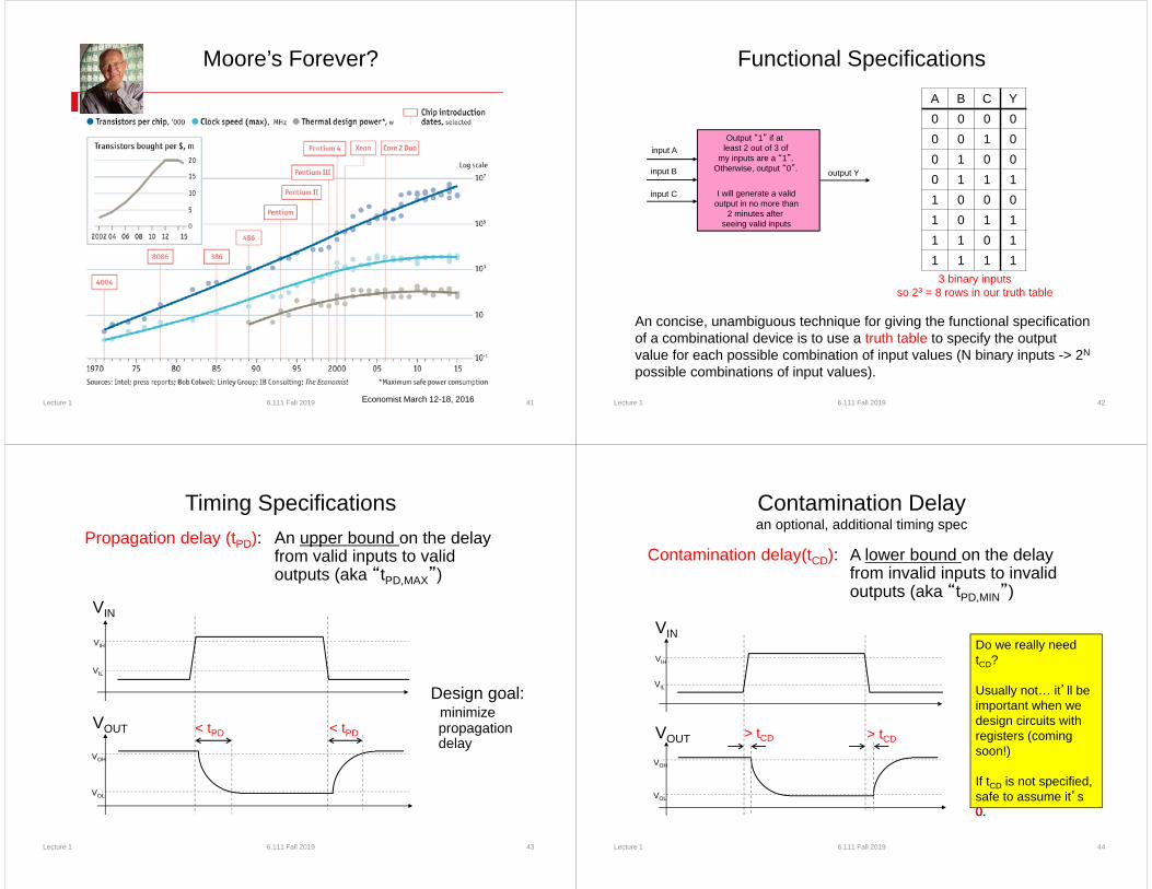
Functional Specifications
Lecture 1 6.111 Fall 2019 42
Output “1” if at least 2 out of 3 of
my inputs are a “1”.Otherwise, output “0”.
I will generate a validoutput in no more than
2 minutes after seeing valid inputs
input A
input B
input C
output Y
A B C Y0 0 0 00 0 1 00 1 0 00 1 1 11 0 0 01 0 1 11 1 0 11 1 1 1
An concise, unambiguous technique for giving the functional specification of a combinational device is to use a truth table to specify the output value for each possible combination of input values (N binary inputs -> 2N
possible combinations of input values).
3 binary inputsso 23 = 8 rows in our truth table
Timing SpecificationsPropagation delay (tPD): An upper bound on the delay
from valid inputs to valid outputs (aka “tPD,MAX”)
Design goal:minimizepropagationdelay
VOUT < tPD< tPD
VIN
VOL
VOH
VIL
VIH
Lecture 1 6.111 Fall 2019 43
Contamination Delayan optional, additional timing spec
VOUT > tCD> tCD
VIN
VOL
VOH
VIL
VIH
0.
Do we really need tCD?
Usually not… it’ll be important when we design circuits with registers (coming soon!)
If tCD is not specified, safe to assume it’s 0.
Contamination delay(tCD): A lower bound on the delay from invalid inputs to invalid outputs (aka “tPD,MIN”)
Lecture 1 6.111 Fall 2019 44

The Combinational Contract
A BA B0 11 0
tPD propagation delaytCD contamination delay
A
B
Must be ___________
Must be ___________
Note:1. No Promises during 2. Default (conservative) spec: tCD = 0
< tPD
> tCD
Lecture 1 6.111 Fall 2019 45
Hardware Implementation
Boolean Logic and State
Building Digital Systems• Goal of 6.111: Building binary digital solutions to
computational problems
Behavioral Description
conversion to binary,Booelan algebra
device selectionand wiring
algorithm selection,flowcharts, etc.
Problem Statement Labs & Design project Product specs
Algorithms, RTL, etc. Flowcharts State transition diagrams
Logic equations Circuit schematics
TTL Gates (AND,OR,XOR…) Modules (counter, shifter,…) Programmable Logic
Lecture 1 6.111 Fall 2019 46
Hardware Implementation
HDL Description
Building Digital Systems with HDLs
Behavioral Description
software-likeprogramming
automated synthesis
algorithm selection,flowcharts, etc.
Problem Statement Labs & Design project Product specs
Algorithms, RTL, etc. Flowcharts State transition diagrams
Verilog code VHDL code
Programmable Logic Custom ASICs
• Logic synthesis using a Hardware Description Language (HDL) automates the most tedious and error-prone aspects of design
Lecture 1 6.111 Fall 2019 47
Hardware structures can be modeled effectively in either VHDL and Verilog. Verilog is similar to c and a bit easier to learn.
Verilog and VHDL
• Created by Gateway Design Automation in 1985; now an IEEE standard
• Initially an interpreted language for gate-level simulation
• Less explicit typing (e.g., compiler will pad arguments of different widths)
• No special extensions for large designs
Commissioned in 1981 by Department of Defense; now an IEEE standard
Initially created for ASIC synthesis
Strongly typed; potential for verbose code
Strong support for package management and large designs
VHDL Verilog
Lecture 1 6.111 Fall 2019 48

Verilog HDL• Misconceptions
– The coding style or clarity does not matter as long as it works – Two different Verilog encodings that simulate the same way will synthesize to the
same set of gates– Synthesis just can’t be as good as a design done by humans
• Shades of assembly language versus a higher level language
• What can be Synthesized– Combinational Functions
• Multiplexors, Encoders, Decoders, Comparators, Parity Generators, Adders, Subtractors, ALUs, Multipliers
• Random logic– Control Logic
• FSMs
• What can’t be Synthesized– Precise timing blocks (e.g., delay a signal by 2ns)– Large memory blocks (can be done, but very inefficient)
• Understand what constructs are used in simulation vs. hardware mapping
Lecture 1 6.111 Fall 2019 49
The FPGA: A Conceptual View• An FPGA is like an electronic breadboard that is wired together by an
automated synthesis tool• Built-in components are called CLB (configurable logic blocks) and
used to build logic blocks.
sel
interconnect
D Q
LUTF(a,b,c,d)G(a,b,c,d)
abcd
RAMADR
R/WDATA
counter
+32
32
32SUM
(for everything else)
Lecture 1 6.111 Fall 2019 50
Lecture 1 6.111 Fall 2019 51
Xilinx FPGA Interconnect Details
Why six transistors?
Synthesis and Mapping for FPGAs
• Infer logic : choose the FPGA CLB that efficiently implement various parts of the HDL code
• Place-and-route: with area and/or speed in mind, choose the needed macros by location and route the interconnect
counter
...always @ (posedge clk)begin
count <= count + 1;end...
“This section of code looks like a counter. My FPGA can synthesize some of those...”
HDL Code Inferred logic
M
M
M
M
M
M
M
M
M
M
M
M
M
M
M
M
M
M
M
M
M
M
M
M
M
M
M
M
M
M
M
M
M
M
M
“This design only uses 10% of the FPGA. Let’s use the CLB in one corner to minimize the distance between blocks.”
Lecture 1 6.111 Fall 2019 52

Summary• Use voltages to encode information• “Digital” encoding
– valid voltage levels for representing “0” and “1”
– forbidden zone avoids mistaking “0” for “1” and vice versa• Noise
– Want to tolerate real-world conditions: NOISE.– Key: tougher standards for output than for input– devices must have gain and have a non-linear VTC
• Combinational devices– Each logic family has Tinkertoy-set simplicity, modularity– predictable composition: “parts work whole thing works”
– static discipline• digital inputs, outputs; restore marginal input voltages• complete functional spec, e.g., a truth table• valid inputs lead to valid outputs in bounded time (<tPD)
Lecture 1 6.111 Fall 2019 53
Lab Checkoff
• Lab check off will be in two groups: Thu or Fri. • Thu group indicated by @G1 or @G2 in grade sheet
Lecture 1 6.111 Fall 2019 54

Lecture 1 Part 2Quick SystemVerilog and Vivado Overview for Lab 1
9/5/2019 6.111 Fall 2019 1
6.111 Thru the Ages
Lecture 1 6.111 Fall 2019 2
Lab kit 1990 aka “digital death” Labkit 2005
Nexys 4 ‐ 2016 PYNQ ‐ 2019***
Things Change….
9/5/2019 6.111 Fall 2019 3
https://www.nature.com/articles/s41586‐019‐1493‐8
Vivado Demo
9/5/2019 6.111 Fall 2019 4
https://web.mit.edu/6.111/volume2/www/f2019/handouts/labs/vivado_quickstart/quickstart.html

What Controls This?
9/5/2019 6.111 Fall 2019 5
• SystemVeriloginterpreted with Vivado
“Verilog” or “SystemVerilog”?• SystemVerilog is a superset of Verilog (just like C++ is a superset of C)
• We will learn/use SystemVerilog (.sv files), however~90% of what we do is just Verilog!
• We’re transitioning to this for 2019 since this is how the field is. It also opens a lot more doors for self‐study:
• SystemVerilog is pretty nice so maybe you’ll arrive organically at needing some of its behaviors in the project
9/5/2019 6.111 Fall 2019 6
Online Verilog/SystemVerilogResources• There are books, but you can figure out most of it from:
• Doing the labs (motivation to have to figure it out)• Formal‐ish online resources (best free tutorials):
• http://www.asic‐world.com/verilog/veritut.html• http://www.asic‐world.com/systemverilog/tutorial.html
• Informal (StackOverflow)
9/5/2019 6.111 Fall 2019 7
How to Think About Designing Logic
• A piece of software/program should be thought of as a set of instructions that are executed roughly sequentially
• You describe what to do with software
9/5/2019 6.111 Fall 2019 8

How to Think About Designing Logic
• A design in a Hardware Description Language (HDL) describes the wiring and placement of components. Think of it is specifying a blueprint for what you want to build
• You describe what to build with HDL
• Everything you describe exists in parallel (sort of)
9/5/2019 6.111 Fall 2019 9
Three Languages, Similar Functionality
9/5/2019 6.111 Fall 2019 10
• Verilog allows us to design hardware in ways similar to how we write programs:
Verilog is Very Low Level
9/5/2019 6.111 Fall 2019 11
• a is one bit• b is one bit• c is one bit
The Verilog implementation is only one‐bit wide by default
ab c
a b c0 0 00 1 11 0 11 1 0
Will most likely get synthesized to or the equivalent:
If we wanted an 8 bit adder:
• We’ll be using Xilinx FPGAs in this class, and in order to do that, we’ll need to use their software development environment Vivado
• Large piece of software that takes care of everything for us
• Lab 1 is designed to get you working with it quickly, but it is going to take a few labs to get to really know it.
9/5/2019 6.111 Fall 2019 12

Vivado QuickStart
• Video shown at beginning• We have a fully‐working project for you to build here: https://web.mit.edu/6.111/volume2/www/f2019/handouts/labs/vivado_quickstart/quickstart.html
• We recommend building it before starting Lab 1 since it has some setup stuff in it.
9/5/2019 6.111 Fall 2019 13
Verilog Gets Turned into a Circuit
9/5/2019 6.111 Fall 2019 14
VivadoSystemVerilog file
Build Processes
Console
Verilog:
9/5/2019 6.111 Fall 2019 15
• Start with this:
This Circuit then Gets Designed
9/5/2019 6.111 Fall 2019 16
Under Synthesis go to:Schematic
Verilog is interpreted into a circuit

Then it gets placed (Implemented)
9/5/2019 6.111 Fall 2019 17
With Implementation Open go to:Windows>Device
Then it gets loaded onto board
9/5/2019 6.111 Fall 2019 18
For Lab 1• The circuits you’ll be building will be purely combinational, meaning they will be stateless
• Current outputs based ONLY on current inputs• No clocks…your designs won’t need to include the concept of time
• This shouldn’t be too bad and should let us focus more on syntax and Vivado rather than the intricacies of other stuff.
9/5/2019 6.111 Fall 2019 19
Practicing Verilog
• Install Vivado (takes up lots of space and requires Windows or Linux)
• Or….
9/5/2019 6.111 Fall 2019 20

Online Verilog/System Verilog
9/5/2019 6.111 Fall 2019 21
edaplayground.com/homeIcarus Verilog
• Works well, but is only Verilog (not SystemVerilog) so a subset of commands we use such as always_ffalways_comb will not be supported
• http://iverilog.icarus.com/
9/5/2019 6.111 Fall 2019 22
Recommendation
• Start Lab 1 as soon as possible (due next week)• Lab 1 and Pset 1 will mutually support one another (Pset 1 is designed to help you do Lab 1)
• Lab 2 is longer, and will come out tomorrow/this weekend early in case you want to get started on it.
9/5/2019 6.111 Fall 2019 23