Lead-free Soldering - PCB Fabrication
13
1 Lead-free Soldering – A Challenge For Base Materials Authors: W. Alberth H. Schumacher Isola GmbH On February 13 th , 2003, the European Parliament and the European Commission announced and published the so-called RoHS directive, dealing with the "Restriction of the use of certain Hazardous Substances" in electrical and electronic equipment. This directive was converted in national laws and from July 1st, 2006 on so-called hazardous substances like mercury, cadmium, lead, chromium VI will be dramatically reduced in industrial products in order to support the waste treatment regulations as well as recycling processes of components. Our industry is also heavily affected due to restriction resp. ban of lead in electronic systems. There are also exceptions defined such as electronic systems being used in medical equipment, control and supervision systems as well as networking infrastructure equipment. Since more than one year the industry is following this direction consequently and will be prepared along the value chain. Leading OEMs and CEMs, also outside Europe, have officially announced to have lead-free soldering implemented earlier than the requested time line. Japanese companies like MATSUSHITA, HITACHI, SONY, PANASONIC are actively working on the lead substitution in their products, European OEMs like SIEMENS, ERICSSON, NOKIA, BOSCH or American OEMs are on the same track. Different lead-free solder alloys have been evaluated for lead- free soldering of pcbs. Picture 1 shows a comparison of the different alloys regarding their melting points. Wolfgang Alberth Director OEM Marketing Europe Location: Dueren Phone: ++49 24 21 80 84 00 Fax: ++49 24 21 8 08 84 00 Wolfgang.Alberth@Isola- Group.com 03.01.2005/he
Transcript of Lead-free Soldering - PCB Fabrication

1
Lead-free Soldering – A Challenge For Base Materials Authors: W. Alberth H. Schumacher Isola GmbH On February 13th, 2003, the European Parliament and the European Commission announced and published the so-called RoHS directive, dealing with the "Restriction of the use of certain Hazardous Substances" in electrical and electronic equipment. This directive was converted in national laws and from July 1st, 2006 on so-called hazardous substances like mercury, cadmium, lead, chromium VI will be dramatically reduced in industrial products in order to support the waste treatment regulations as well as recycling processes of components. Our industry is also heavily affected due to restriction resp. ban of lead in electronic systems. There are also exceptions defined such as electronic systems being used in medical equipment, control and supervision systems as well as networking infrastructure equipment. Since more than one year the industry is following this direction consequently and will be prepared along the value chain. Leading OEMs and CEMs, also outside Europe, have officially announced to have lead-free soldering implemented earlier than the requested time line. Japanese companies like MATSUSHITA, HITACHI, SONY, PANASONIC are actively working on the lead substitution in their products, European OEMs like SIEMENS, ERICSSON, NOKIA, BOSCH or American OEMs are on the same track. Different lead-free solder alloys have been evaluated for lead-free soldering of pcbs. Picture 1 shows a comparison of the different alloys regarding their melting points.
Wolfgang Alberth Director OEM Marketing Europe Location: Dueren Phone: ++49 24 21 80 84 00 Fax: ++49 24 21 8 08 84 00 [email protected] 03.01.2005/he

2
Since the actual solder temperature is 20 – 30 °C higher than the melting point of the alloy, the peak temperature at soldering will increase from ~ 215 ± 10 °C to 245 ± 10 °C maximum for appr. 20 seconds (reflow convection oven). A typical temperature-time profile for a reflow process is shown in graph 2.

3
What does it mean for the base material of a pcb, if the peak
temperature increases from 220 °C up to 250/260 °C? What are problems that can occur and how to avoid them?
The thermal behaviour of a base material is mainly determined by:
the resin type
the crosslinking agent
the degree of crosslinking
the decomposition temperature of the resin system
adhesion of resin to carrier material (glass cloth)
additives f. e. fillers
Today, mostly used resin types are di-, tetra- or multifunctional
epoxy resins with a Tg ranging from 135 up to 180 °C. Curing agents used for epoxy resins are dicyandiamide or novolacs
(phenolic cured). The degree of crosslinking is defined by the temperature and corresponding time the laminate sees during the press process.
The adhesion of the resin to the glass fabric is defined by the finish type on the glass fiber. Finally, the thermal behaviour of
base materials in thermal cycling tests can be improved by adding appropriate fillers to the resin system.
Predominantly, the Tg value was the only criteria for thermal
performance of a resin system. This has been proven to be inadequate, since the Tg is only one out of other characteristics
which all together give the full picture of thermal reliability needed f. e. at lead-free soldering. In other words: The Tg tells you really little serious about the thermal reliability of the polymer. More important characteristics to describe the thermal
behaviour are the T-260 resp. T-288 tests, thermal decomposition temperature Td and the thermal degradation at
4
elevated iso thermal temperatures of the resin matrix in a defined
time window (for example 1 hour at 220 °C, 240 °C, ...).
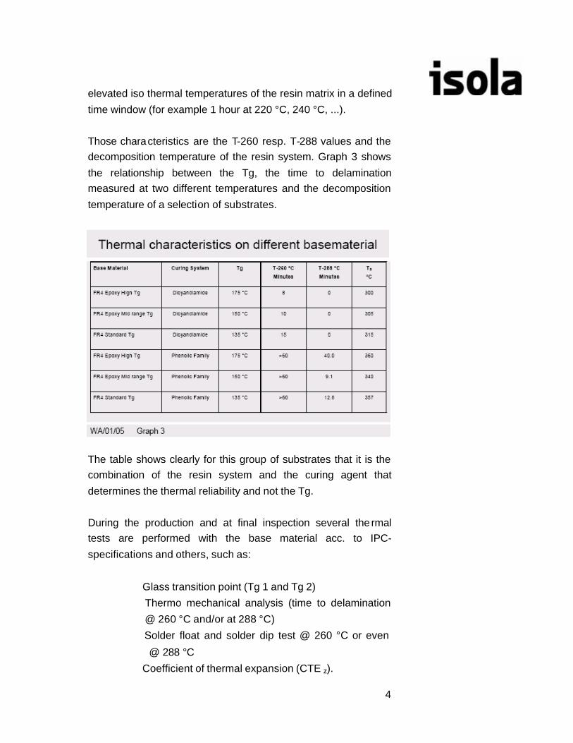
Those characteristics are the T-260 resp. T-288 values and the decomposition temperature of the resin system. Graph 3 shows
the relationship between the Tg, the time to delamination measured at two different temperatures and the decomposition
temperature of a selection of substrates.
The table shows clearly for this group of substrates that it is the combination of the resin system and the curing agent that
determines the thermal reliability and not the Tg.
During the production and at final inspection several the rmal tests are performed with the base material acc. to IPC-
specifications and others, such as:
Glass transition point (Tg 1 and Tg 2)
Thermo mechanical analysis (time to delamination
@ 260 °C and/or at 288 °C)
Solder float and solder dip test @ 260 °C or even
@ 288 °C
Coefficient of thermal expansion (CTE z).

5
The criteria are degree of curing (Tg resp. ? Tg) and
delamination/separation in the base material.
Since most of the a. m functional testings are performed and passed at temperatures and conditions @ 260 °C and higher
from a laminate point of view, the lead-free soldering is not being considered as a problem.
Can this situation change on MLB-level? Yes, it can.
Investigations have shown that f. e. the time to delamination at 260 °C (T260 –test in TMA) on laminate level can last from 10 up to more than 60 minutes, whereas on MLB-level the time can be
significantly lower for the same resin matrix.
Manufacturing processes that are needed for MLB production can influence the thermal behaviour during lead-free soldering
(f. e. black/brown oxide or alternatives, pressing at relamination, drilling parameters, hole cleaning, moisture pick-up etc).
Furthermore, the design of the pcb also has a great influence on
the thermal resistance during lead-free soldering. Remaining moisture or chemicals in the MLB can also generate
problems/delaminations due to increased vapor pressure at elevated temperatures.
6
The graph shows clearly that the vapor pressure is more than 2 x
higher by increasing the solder temperature from 220 °C to 265 °C. An appropriate drying process prior to lead-free soldering is
therefore strongly recommended.
Remark: Resin systems with an appropriate filler can increase the thermal resistance due to reduced humidity pick-up and a
lower z-axis expansion to protect the material against thermal-mechanical stress.
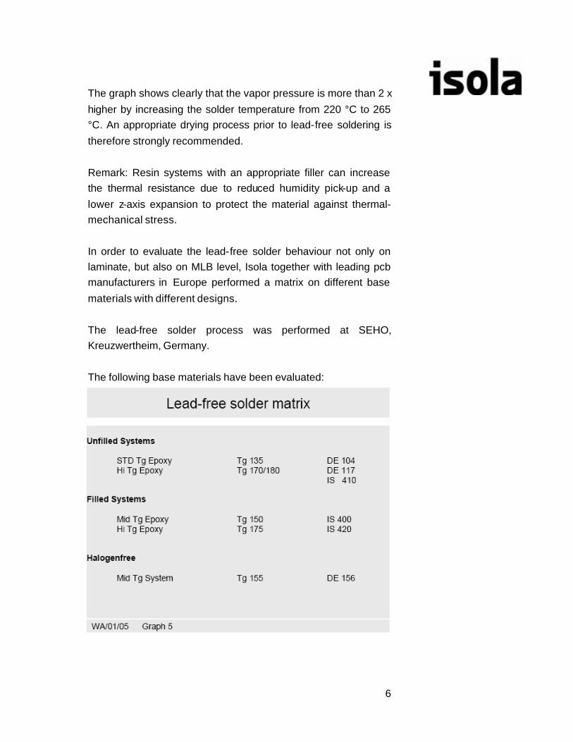
In order to evaluate the lead-free solder behaviour not only on laminate, but also on MLB level, Isola together with leading pcb manufacturers in Europe performed a matrix on different base
materials with different designs.
The lead-free solder process was performed at SEHO, Kreuzwertheim, Germany.
The following base materials have been evaluated:

7
The boards have been soldered without devices. The lead-free
solder process included the following process steps:
2 x wave soldering 2 x – 4 x reflow.
The solder alloy being used at wave soldering contained
99.2 % Sn
0.1 % Ni 0.7 % Cu The melting point of this alloy is 227 °C, whereas the solder
temperature was @ 265 °C with a contact time of 3 – 4 sec. The MLB was preheated prior to soldering up to 130 – 140 °C.
The solder profiles of the wave solder process and the reflow
process are shown in graph (6) and graph (7).

8
After several reflow processes the MLB's have been sectioned
and inspected. The results will be introduced and discussed in detail during the lecture.

9

10

11

12

13
Biographies
Wolfgang Alberth is Director OEM Marketing Europe for Isola.
He joined Isola in 1996 and held several Management positions
in both, manufacturing and product development. Previously he was working 14 years for IBM in Germany as Process Engineer
for pcb production and later being involved in Management of pcb process and product developments for standard and
advanced technologies. Wolfgang holds a B. Sc. Degree in metallurgy from University of
Applied Science in Aalen, Germany.
Hans Schumacher is Director Technology-Development Europe
for Isola. He joined Isola in 1984 being responsible for analytical lab/materials testings and product development.
Hans holds a B. Sc Degree in chemical engineering from University of Applied Science in Aachen, Germany.