
Laser-illuminated nanohole arrays for multiplex...
6
Laser-illuminated nanohole arrays for multiplex plasmonic microarray sensing Antoine Lesuffleur, Hyungsoon Im, Nathan C. Lindquist, Kwan Seop Lim, Sang-Hyun Oh* Laboratory of Nanostructures and Biosensing, Department of Electrical and Computer Engineering University of Minnesota, Twin Cities, Minneapolis, MN 55455 USA *E-mail: [email protected] , http://nanobio.umn.edu Abstract: Surface plasmon resonance (SPR) imaging is a powerful technique for high-throughput, real-time, label-free characterization of molecular interactions in a microarray format. In this paper, we demonstrate SPR imaging with nanohole arrays illuminated by a laser source. Periodic nanoholes couple incident photons into SPs, obviating the need for the prism used in conventional SPR instruments, while a laser source provides the intensity, stability and spectral coherence to improve the detection sensitivity. The formation of a self-assembled monolayer of alkanethiolates on gold changed the laser transmission by more than 35%, and binding kinetics were measured in parallel from a 5×3 microarray of nanohole sensors. These results demonstrate the potential of nanohole sensors for high-throughput SPR imaging on microarrays. ©2008 Optical Society of America OCIS codes: (040.1240) Array detectors; (240.6680) Surface plasmons. References and links 1. B. Liedberg, C. Nylander and I. Lunström, “Surface plasmon resonance for gas detection and biosensing,” Sens. Actuators 4, 299 (1983). 2. E. Yeatman and E.A. Ash, “Surface-plasmon microscopy,” Electron Lett. 23, 1091 (1987). 3. B. Rothenhäusler and W. Knoll, “Surface-plasmon microscopy,” Nature 332, 615 (1988). 4. J.S. Shumaker-Parry, R. Aebersold and C.T. Campbell “Parallel, quantitative measurement of protein binding to a 120-element double-stranded DNA array in real time using surface plasmon resonance microscopy,” Anal. Chem. 76, 2071 (2004). 5. E.A. Smith and R.M. Corn, “Surface plasmon resonance imaging as a tool to monitor biomolecular interactions in an array based format,” Appl. Spectrosc. 57 (11), 320A (2003). 6. E. Fu, J. Foley and P. Yager, “Wavelength-tunable surface plasmon resonance microscope,” Rev. Sci. Instrum. 74 (6), 3182 (2003). 7. T.W. Ebbesen, H.J. Lezec, H.F. Ghaemi, T. Thio and P.A. Wolff, “Extraordinary optical transmission through subwavelength hole arrays,” Nature 391, 667 (1998). 8. L. Martin-Moreno, F.J. Garcia-Vidal, H.J. Lezec, K.M. Pellerin, T. Thio, J.B. Pendry and T.W. Ebbesen, “Theory of extraordinary optical transmission through subwavelength hole arrays,” Phys. Rev. Lett. 86, 1114 (2001). 9. A.G. Brolo, R. Gordon, B. Leathem and K.L. Kavanagh, “Surface plasmon sensor based on the enhanced light transmission through arrays of nanoholes in gold films,” Langmuir 20, 4813 (2004). 10. A. De Leebeeck, L.K.S. Kumar, V. de Lange, D. Sinton, R. Gordon and A.G. Brolo, “On-chip surface- based detection with nanohole arrays,” Anal. Chem. 79, 4094 (2007). 11. A. Lesuffleur, H. Im, N.C. Lindquist and S.-H. Oh, “Periodic nanohole arrays with shape-enhanced plasmon resonance as real-time biosensors,” Appl. Phys. Lett. 90, 243110 (2007). 12. L. Pang, G.M. Hwang, B. Slutsky and Y. Fainman “Spectral sensitivity of two-dimensional nanohole array surface plasmon polariton resonance sensor,” Appl. Phys. Lett. 91, 123115 (2007). 13. Y.N. Xia and G.M. Whitesides, “Soft lithography,” Angew. Chem. Int. Ed. 37, 550 (1998). 14. M. Mrksich, G. Sigal and G.M. Whitesides, “Surface plasmon resonance permits in situ measurement of protein adsorption on self-assembled monolayers of alkanethiolates on gold,” Langmuir 11, 4383 (1995). 15. T.M. Chinowsky, T. Mactutis, E. Fu and P. Yager, “Optical and electronic design for a high-performance surface plasmon resonance imager,” Proceedings of SPIE, Vol. 5261, 173 (2004). 16. L.S. Jung, C.T. Campbell, T.M. Chinowsky, M.N. Mar and S.S. Yee, “Quantitative interpretation of the response of surface plasmon resonance sensors to adsorbed films,” Langmuir 14, 5636 (1998). #89461 - $15.00 USD Received 7 Nov 2007; revised 19 Dec 2007; accepted 20 Dec 2007; published 2 Jan 2008 (C) 2008 OSA 7 January 2008 / Vol. 16, No. 1 / OPTICS EXPRESS 219
Transcript of Laser-illuminated nanohole arrays for multiplex...

Laser-illuminated nanohole arrays for multiplex plasmonic microarray sensing
Antoine Lesuffleur, Hyungsoon Im, Nathan C. Lindquist, Kwan Seop Lim, Sang-Hyun Oh*
Laboratory of Nanostructures and Biosensing, Department of Electrical and Computer Engineering University of Minnesota, Twin Cities, Minneapolis, MN 55455 USA
*E-mail: [email protected], http://nanobio.umn.edu
Abstract: Surface plasmon resonance (SPR) imaging is a powerful technique for high-throughput, real-time, label-free characterization of molecular interactions in a microarray format. In this paper, we demonstrate SPR imaging with nanohole arrays illuminated by a laser source. Periodic nanoholes couple incident photons into SPs, obviating the need for the prism used in conventional SPR instruments, while a laser source provides the intensity, stability and spectral coherence to improve the detection sensitivity. The formation of a self-assembled monolayer of alkanethiolates on gold changed the laser transmission by more than 35%, and binding kinetics were measured in parallel from a 5×3 microarray of nanohole sensors. These results demonstrate the potential of nanohole sensors for high-throughput SPR imaging on microarrays.
©2008 Optical Society of America
OCIS codes: (040.1240) Array detectors; (240.6680) Surface plasmons.
References and links
1. B. Liedberg, C. Nylander and I. Lunström, “Surface plasmon resonance for gas detection and biosensing,” Sens. Actuators 4, 299 (1983).
2. E. Yeatman and E.A. Ash, “Surface-plasmon microscopy,” Electron Lett. 23, 1091 (1987). 3. B. Rothenhäusler and W. Knoll, “Surface-plasmon microscopy,” Nature 332, 615 (1988). 4. J.S. Shumaker-Parry, R. Aebersold and C.T. Campbell “Parallel, quantitative measurement of protein
binding to a 120-element double-stranded DNA array in real time using surface plasmon resonance microscopy,” Anal. Chem. 76, 2071 (2004).
5. E.A. Smith and R.M. Corn, “Surface plasmon resonance imaging as a tool to monitor biomolecular interactions in an array based format,” Appl. Spectrosc. 57 (11), 320A (2003).
6. E. Fu, J. Foley and P. Yager, “Wavelength-tunable surface plasmon resonance microscope,” Rev. Sci. Instrum. 74 (6), 3182 (2003).
7. T.W. Ebbesen, H.J. Lezec, H.F. Ghaemi, T. Thio and P.A. Wolff, “Extraordinary optical transmission through subwavelength hole arrays,” Nature 391, 667 (1998).
8. L. Martin-Moreno, F.J. Garcia-Vidal, H.J. Lezec, K.M. Pellerin, T. Thio, J.B. Pendry and T.W. Ebbesen, “Theory of extraordinary optical transmission through subwavelength hole arrays,” Phys. Rev. Lett. 86, 1114 (2001).
9. A.G. Brolo, R. Gordon, B. Leathem and K.L. Kavanagh, “Surface plasmon sensor based on the enhanced light transmission through arrays of nanoholes in gold films,” Langmuir 20, 4813 (2004).
10. A. De Leebeeck, L.K.S. Kumar, V. de Lange, D. Sinton, R. Gordon and A.G. Brolo, “On-chip surface-based detection with nanohole arrays,” Anal. Chem. 79, 4094 (2007).
11. A. Lesuffleur, H. Im, N.C. Lindquist and S.-H. Oh, “Periodic nanohole arrays with shape-enhanced plasmon resonance as real-time biosensors,” Appl. Phys. Lett. 90, 243110 (2007).
12. L. Pang, G.M. Hwang, B. Slutsky and Y. Fainman “Spectral sensitivity of two-dimensional nanohole array surface plasmon polariton resonance sensor,” Appl. Phys. Lett. 91, 123115 (2007).
13. Y.N. Xia and G.M. Whitesides, “Soft lithography,” Angew. Chem. Int. Ed. 37, 550 (1998). 14. M. Mrksich, G. Sigal and G.M. Whitesides, “Surface plasmon resonance permits in situ measurement of
protein adsorption on self-assembled monolayers of alkanethiolates on gold,” Langmuir 11, 4383 (1995). 15. T.M. Chinowsky, T. Mactutis, E. Fu and P. Yager, “Optical and electronic design for a high-performance
surface plasmon resonance imager,” Proceedings of SPIE, Vol. 5261, 173 (2004). 16. L.S. Jung, C.T. Campbell, T.M. Chinowsky, M.N. Mar and S.S. Yee, “Quantitative interpretation of the
response of surface plasmon resonance sensors to adsorbed films,” Langmuir 14, 5636 (1998).
#89461 - $15.00 USD Received 7 Nov 2007; revised 19 Dec 2007; accepted 20 Dec 2007; published 2 Jan 2008
(C) 2008 OSA 7 January 2008 / Vol. 16, No. 1 / OPTICS EXPRESS 219

17. For a high signal-to-noise ratio, it is also important that the cut-off wavelength of a single nanohole is smaller than the laser wavelength in water, which ensures that direct transmission through holes, as opposed to SP-mediated transmission, does not contribute significantly to the background noise.
18. N. Ramachandran, E. Hainsworth, B. Bhullar, S. Eisenstein, B. Rosen, A. Lau, J.C. Walter and J. LaBaer, “Self-assembling protein microarrays” Science 305, 86 (2004).
1. Introduction
Surface plasmon resonance (SPR) sensing is the gold standard for measuring the binding kinetics of biomolecules [1]. In this technique, immobilized molecules are contacted by buffer containing ligands, and changes in the local refractive index due to the bound ligands are detected as a shift in the SPR excitation angle. In conventional SPR instruments, e.g. BIAcoreTM, a convergent light cone illuminates the detection spot via prism coupling in a total internal reflection mode, known as the Kretschmann configuration, and the angular distribution of the reflected light intensity is measured in real time. Using this label-free approach, binding kinetics (on/off rates and equilibrium constants) can be precisely measured and the concentrations of ligands present in complex mixtures quantified. In various formats, the technique has found wide applications in pharmaceutical development (small molecules and proteins) as well as in basic research. While this technique has been successfully commercialized, even the most advanced machines are limited in sample throughput and the volume/mass of sample required. For large-scale studies of protein-protein or protein-nucleic acid interactions on a microarray, a new class of high-throughput instruments are needed that are capable of simultaneously measuring thousands of molecular interactions. SPR microscopy [2,3] is one such technique with multiplex screening capability, wherein a refractive index variation across a sample surface, e.g. microarray, due to molecular binding events is translated into a contrast distribution in the reflected image that is captured by a charge coupled device (CCD) camera. Several research groups have demonstrated SPR imaging with the Kretschmann configuration [4,5,6], but the prism coupling method results in a tilted image plane with a narrow field of view, i.e. a small array size, and prohibits the use of high numerical aperture (NA) optics and the potential for miniaturization.
In 1998, Ebbesen et al. reported that light transmission through periodic sub-wavelength hole arrays milled in a gold or silver film could be far more efficient than had been predicted by the conventional theories [7]. Subsequent work [8] has confirmed that SPs excited on both sides of the metal surface resonantly couple through the sub-wavelength holes, which enhances the light transmission for specific wavelengths depending on the periodicity of the array and the dielectric function of both the metal and the surrounding dielectric. Periodic nanohole arrays show potential for SPR sensing, since they can directly couple incident light into SPs, obviating the need for bulky prism coupling used in conventional SPR instruments. Brolo et al. [9] and De Leebeeck et al. [10] showed the feasibility of using periodic nanoholes for biosensing and observed a spectral shift after the immobilization of molecules on gold using a broadband source and a spectrometer. Recently, we have demonstrated real-time measurements of molecular binding using shape-enhanced nanohole arrays in a flow cell [11]. Pang et al. studied the spectral sensitivity of nanohole sensors [12]. Besides eliminating a coupling prism, nanohole arrays bring a number of other advantages to array-based SPR imaging: the small footprint of each sensing element (<10 μm in width), the use of high NA optics for improved resolution, the much simplified optical alignment, and the potential for miniaturization. To our best knowledge, real-time multiplex biosensing using arrays of nanoholes, a laser source and an imaging sensor has not yet been reported.
In this paper, we present a sensor array made of nanoholes in a gold film for SPR imaging. Each sensing spot of the larger microarray consists of a single 16×16 nanohole array, with a footprint of 30-40 μm2. A HeNe laser beam illuminates the array and the transmitted light intensity is measured in real-time using a CCD camera. These results show the possibility of multiplex SPR sensing using nanoholes arrays.
#89461 - $15.00 USD Received 7 Nov 2007; revised 19 Dec 2007; accepted 20 Dec 2007; published 2 Jan 2008
(C) 2008 OSA 7 January 2008 / Vol. 16, No. 1 / OPTICS EXPRESS 220

2. Experimental methods
Nanohole arrays were milled using an FEI focused ion beam on a 100-nm-thick gold film with a 5 nm Cr adhesion layer patterned on a standard glass slide. The diameter of each nanohole was 200 nm with the periodicity of the array ranging from 380 nm to 460 nm, which tuned the sensitive detection region of the transmission spectrum (the area with the highest slope) to the wavelength of a HeNe laser in aqueous medium. Each sensing element, shown in Fig. 1a, consists of a 16×16 nanohole array with a footprint 30-40 μm2. A 5×3 sensor array was made, shown partly in Fig. 1(b), wherein each sensing element is separated by 50 μm from the others. PDMS soft lithography [13] was used to fabricate the microfluidic flow cell. The negative-tone master mold of the channel was patterned on a silicon wafer using a SU-8 photoresist, which produced 100 μm deep channels. The surfaces of the PDMS channel and the sample slide were treated with O2 plasma and covalently bonded to seal the flow channel (Fig. 1(c)).
A self-assembled monolayer (SAM) of alkanethiolates [14] was used as a model system to characterize molecular binding kinetics on the gold surface of the nanohole array sensor. A 4 mM SAM solution was prepared with 11-amino-1-undecanethiol, hydrochloride in DI water. For real-time kinetic measurements, the flow cell was filled with SAM using a syringe pump at a flow rate of 3 μL/min.
Fig. 1. (a) Scanning electron microscopy (SEM) image of a 16×16 nanohole array with a 200 nm hole size and 380 nm periodicity. (b) A bright-field microscope image of 5×3 microarray of nanohole arrays (partially shown). Each sensing element, a 16×16 nanoholes array as in (a), is separated by 50 μm. (c) The PDMS chip, shown with microfluidic flow cells and tubing.
Figure 2 shows the schematic of the experimental setup. For detection, a Nikon Eclipse
LV100 microscope was used. A linearly polarized HeNe laser beam illuminated the sample slide from underneath, and the transmitted beam was collected using a 10x microscope objective (NA=0.3) and imaged using a Photometrics HQ2 cooled CCD camera. CCD images were acquired using a software-controlled shutter (15 msec integration time) with an interval of 5 minutes over the course of 4 hours. The transmitted laser intensity was integrated over each sensing element area using image analysis software.
Fig. 2. Schematic of the experimental setup for real time multiplex imaging.
3. Theory
In an SPR microscopy setup using a prism coupling, an incident beam illuminates the sensing surface at a sizeable tilt angle, causing the reflected beam to have a wide range of focal depths depending on the spatial position on the image plane of a CCD sensor. The extended depth-of-
#89461 - $15.00 USD Received 7 Nov 2007; revised 19 Dec 2007; accepted 20 Dec 2007; published 2 Jan 2008
(C) 2008 OSA 7 January 2008 / Vol. 16, No. 1 / OPTICS EXPRESS 221
field and the varying optical path length caused by the prism limits the lateral size of the object, e.g., microarray, that can be imaged with high quality. A clever optical design such as the Scheimpflug imaging scheme [15] may be used to focus the image on a tilted plane, but its implementation is experimentally difficult. It is also time-consuming to align optics to find the optimal incident illumination angle. In contrast, nanohole arrays use a collinear transmission setup for imaging, which tremendously simplifies the optical alignment, reduces the system footprint, and enables the use of high-NA optics.
A periodic array of nanoholes acts as a two-dimensional grating coupler that converts the incident photons into SPs. Here, the grating momentum wavevectors of the periodic structure are needed to fulfill the energy and momentum conservation between photons and SPs. Although the exact mechanisms of the enhanced optical transmission effect through such nanoholes are still being debated, it is generally accepted that the incident photons, via coupling through the periodic nanoholes, are converted to SPs which couple through the film and are re-radiated from the opposite side as photons by just the reverse process [8]. Since this resonant transmission effect occurs through the excitation and propagation of SPs along the metal-dielectric interface, it is sensitive to the refractive index changes near the interface, as in conventional prism-based SPR sensors.
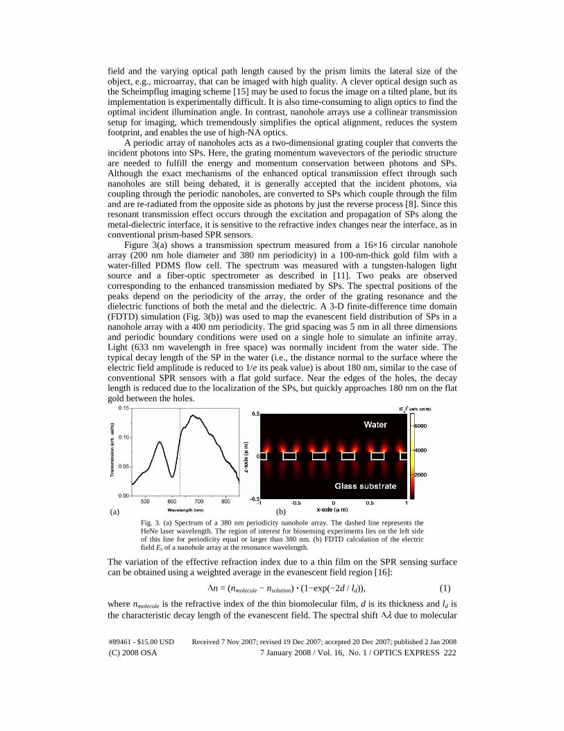
Figure 3(a) shows a transmission spectrum measured from a 16×16 circular nanohole array (200 nm hole diameter and 380 nm periodicity) in a 100-nm-thick gold film with a water-filled PDMS flow cell. The spectrum was measured with a tungsten-halogen light source and a fiber-optic spectrometer as described in [11]. Two peaks are observed corresponding to the enhanced transmission mediated by SPs. The spectral positions of the peaks depend on the periodicity of the array, the order of the grating resonance and the dielectric functions of both the metal and the dielectric. A 3-D finite-difference time domain (FDTD) simulation (Fig. 3(b)) was used to map the evanescent field distribution of SPs in a nanohole array with a 400 nm periodicity. The grid spacing was 5 nm in all three dimensions and periodic boundary conditions were used on a single hole to simulate an infinite array. Light (633 nm wavelength in free space) was normally incident from the water side. The typical decay length of the SP in the water (i.e., the distance normal to the surface where the electric field amplitude is reduced to 1/e its peak value) is about 180 nm, similar to the case of conventional SPR sensors with a flat gold surface. Near the edges of the holes, the decay length is reduced due to the localization of the SPs, but quickly approaches 180 nm on the flat gold between the holes.
Fig. 3. (a) Spectrum of a 380 nm periodicity nanohole array. The dashed line represents the HeNe laser wavelength. The region of interest for biosensing experiments lies on the left side of this line for periodicity equal or larger than 380 nm. (b) FDTD calculation of the electric field Ez of a nanohole array at the resonance wavelength.
The variation of the effective refraction index due to a thin film on the SPR sensing surface can be obtained using a weighted average in the evanescent field region [16]:
Δn = (nmolecule − nsolution) · (1−exp(−2d / ld)), (1)
where nmolecule is the refractive index of the thin biomolecular film, d is its thickness and ld is the characteristic decay length of the evanescent field. The spectral shift Δλ due to molecular
(a) (b)
#89461 - $15.00 USD Received 7 Nov 2007; revised 19 Dec 2007; accepted 20 Dec 2007; published 2 Jan 2008
(C) 2008 OSA 7 January 2008 / Vol. 16, No. 1 / OPTICS EXPRESS 222
binding is then given by Δλ=S(Δn) where S is the spectral sensitivity. S depends on the geometrical parameters of the nanohole array and of the dielectric functions of the media. In case of multiplex SPR imaging, it can be more useful to measure the variation of the transmitted intensity IT at a fixed detection wavelength in real time, which is given by:
ΔIT = −(dIT / dλ) · S(Δn) (2)
For laser-based SPR imaging, the sensitivity not only depends on the spectral sensitivity but also on the slope dIT/dλ, i.e. the sharpness of the resonance peak.
4. Results and discussion
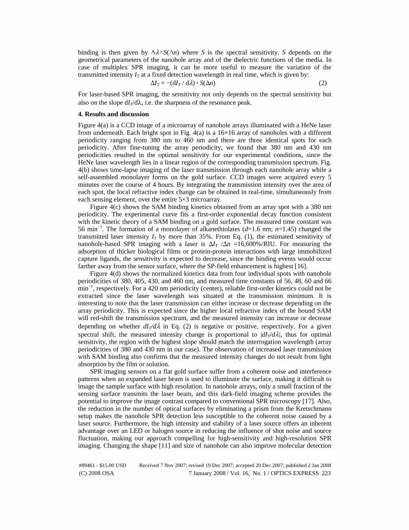
Figure 4(a) is a CCD image of a microarray of nanohole arrays illuminated with a HeNe laser from underneath. Each bright spot in Fig. 4(a) is a 16×16 array of nanoholes with a different periodicity ranging from 380 nm to 460 nm and there are three identical spots for each periodicity. After fine-tuning the array periodicity, we found that 380 nm and 430 nm periodicities resulted in the optimal sensitivity for our experimental conditions, since the HeNe laser wavelength lies in a linear region of the corresponding transmission spectrum. Fig. 4(b) shows time-lapse imaging of the laser transmission through each nanohole array while a self-assembled monolayer forms on the gold surface. CCD images were acquired every 5 minutes over the course of 4 hours. By integrating the transmission intensity over the area of each spot, the local refractive index change can be obtained in real-time, simultaneously from each sensing element, over the entire 5×3 microarray.
Figure 4(c) shows the SAM binding kinetics obtained from an array spot with a 380 nm periodicity. The experimental curve fits a first-order exponential decay function consistent with the kinetic theory of a SAM binding on a gold surface. The measured time constant was 56 min−1. The formation of a monolayer of alkanethiolates (d=1.6 nm; n=1.45) changed the transmitted laser intensity IT by more than 35%. From Eq. (1), the estimated sensitivity of nanohole-based SPR imaging with a laser is ΔIT /Δn =16,600%/RIU. For measuring the adsorption of thicker biological films or protein-protein interactions with large immobilized capture ligands, the sensitivity is expected to decrease, since the binding events would occur farther away from the sensor surface, where the SP-field enhancement is highest [16].
Figure 4(d) shows the normalized kinetics data from four individual spots with nanohole periodicities of 380, 405, 430, and 460 nm, and measured time constants of 56, 48, 60 and 66 min−1, respectively. For a 420 nm periodicity (center), reliable first-order kinetics could not be extracted since the laser wavelength was situated at the transmission minimum. It is interesting to note that the laser transmission can either increase or decrease depending on the array periodicity. This is expected since the higher local refractive index of the bound SAM will red-shift the transmission spectrum, and the measured intensity can increase or decrease depending on whether dIT/dλ in Eq. (2) is negative or positive, respectively. For a given spectral shift, the measured intensity change is proportional to |dIT/dλ|, thus for optimal sensitivity, the region with the highest slope should match the interrogation wavelength (array periodicities of 380 and 430 nm in our case). The observation of increased laser transmission with SAM binding also confirms that the measured intensity changes do not result from light absorption by the film or solution.
SPR imaging sensors on a flat gold surface suffer from a coherent noise and interference patterns when an expanded laser beam is used to illuminate the surface, making it difficult to image the sample surface with high resolution. In nanohole arrays, only a small fraction of the sensing surface transmits the laser beam, and this dark-field imaging scheme provides the potential to improve the image contrast compared to conventional SPR microscopy [17]. Also, the reduction in the number of optical surfaces by eliminating a prism from the Kretschmann setup makes the nanohole SPR detection less susceptible to the coherent noise caused by a laser source. Furthermore, the high intensity and stability of a laser source offers an inherent advantage over an LED or halogen source in reducing the influence of shot noise and source fluctuation, making our approach compelling for high-sensitivity and high-resolution SPR imaging. Changing the shape [11] and size of nanohole can also improve molecular detection
#89461 - $15.00 USD Received 7 Nov 2007; revised 19 Dec 2007; accepted 20 Dec 2007; published 2 Jan 2008
(C) 2008 OSA 7 January 2008 / Vol. 16, No. 1 / OPTICS EXPRESS 223

sensitivity. Given that each sensing element is separated by 50 μm in our array, the theoretical packing density is 40,000 spots in a 1 cm2 area, which shows promise to address the challenge of profiling the human proteome (>30,000 proteins) on a chip.
Fig. 4 (a) A CCD image of the arrays during the real time measurement. The arrows indicates the array used for extracting the kinetic data. (b) Time-lapsed imaging of the first row in the microarray. (c) Transmitted intensity measured from the CCD images. Squares represent experimental data, which are fitted with an exponential, showing first-order binding kinetics. (d) (Colors online) Summary of the kinetics measured for 4 array periodicities.
5. Conclusions
We have demonstrated an SPR microarray sensor based on nanohole arrays. By illuminating the array sensor with a laser beam and capturing the transmitted light with time-lapsed CCD imaging, the molecular binding kinetics can be simultaneously recorded from each spot in the microarray. Nanohole sensor arrays can launch SPs without requiring a prism used in the Kretschmann setup, which tremendously simplifies the design and alignment of high-quality imaging optics. The small footprint (<10 μm in width) of each sensing element and the very high packing density achievable with this technique show promise for miniaturization and multiplex screening. In addition, a HeNe laser source was used to illuminate the arrays and to perform real-time measurements of the formation of a self-assembled monolayer on gold. The detection sensitivity of 16,600%/RIU demonstrates the potential of nanoholes as a multiplex microarray detector that features high resolution and sensitivity with a simpler optical setup. These results demonstrate that nanohole arrays could be combined with DNA or protein microarray technologies [18] for large-scale investigation of biomolecular interactions, which is important for drug discovery, proteomics and systems biology.
Acknowledgment
The authors acknowledge James Leger for helpful discussions and Anand Gopinath for allowing access to the FDTD simulation tool. H. Im acknowledges 3M Science and Technology Fellowship and N.C. Lindquist acknowledges NIH Biotechnology training grant T32-GM008347. Device fabrication was performed at the UMN NanoFabrication Center, which receives support from the NSF National Nanotechnology Infrastructure Network.
Nanohole periodicity (nm) 380 405 420 430 460
50 μm
(a) (b)
(c) (d)
#89461 - $15.00 USD Received 7 Nov 2007; revised 19 Dec 2007; accepted 20 Dec 2007; published 2 Jan 2008
(C) 2008 OSA 7 January 2008 / Vol. 16, No. 1 / OPTICS EXPRESS 224