Polycrystalline Silicon Films with Nanometer- Sized Dense ...
Upload
truongdieuCategory
view
221download
0
Laser beam induced currents in polycrystalline silicon thin films prepared byinterference laser crystallization
B. Rezek ∗†, C. E. Nebel, M. StutzmannWalter Schottky Institut, Technische Universitat Munchen, Am Coulombwall, 85748 Garching, Germany
(January 21, 2002)
Polycrystalline silicon layers are prepared by interference laser crystallization (ILC) in the superlateral growth regime (SLG). To characterize their microscopic photoelectrical properties, light beaminduced current (LBIC) is used, employing a focused laser beam for local generation of photocarriersin the layers with spatial resolution of ≈ 0.4 µm. The results are correlated with surface morphologyobtained by atomic force microscopy. In the single pulse ILC, the temperature profiles are optimizedby changing the proportion of interfering beam intensities. The typical grains are of triangular shape,with a length of 1.5 µm and width < 0.5 µm. The photocurrent response is dominated by variationsin the sample thickness. In the multiple pulse ILC, thin films with grains of quadratic shape and ofsize exceeding 5 µm are obtained by shifting the sample through an interference pattern, thus takingadvantage of lateral epitaxial regrowth. Here, by use of a lock–in, LBIC can detect position andlocal electronic properties of individual grain boundaries. Grain boundaries are clearly identified by180 shifts of the photocurrent phase close to maxima of photocurrent amplitude. The photocurrentis attributed to local fields at grain boundaries. These fields extend about 1.4 µm into the grains.The barrier height at the boundary is about 110 mV.
73.61.Cw, 73.50.Gr, 68.37.-d, 68.55.Ac
I. INTRODUCTION
Silicon deposited as a thin film has found use in large area electronic devices, the most prominent representativesof which are flat panel displays and solar cells. Up to now, on low cost substrates such as glass or polymer foilssilicon thin films can be grown only in amorphous or microcrystalline form and the electronic transport properties ofthese films do not reach the quality of monocrystalline silicon. Solar cell and thin film transistor applications requirepolycrystalline silicon thin films of high electronic quality, a prerequisite for which is a large grain size and a lowdefect density. Since the average grain size achieved by conventional chemical vapour deposition techniques remainsin the range of several tens of nanometers, which for instance limits mobility of charge carriers to about 1 cm2/Vscompared to 1300 cm2/Vs in monocrystalline silicon, different methods for crystallization of thin amorphous siliconfilms have been investigated over the last few years.
Solid phase crystallization can produce rather large grains [1], but the process takes hours to complete and tem-peratures necessary during the growth (500 − 600C) are too high for most low cost substrates. In continuous wavelaser processing [2], the growth of large grains is achieved by scanning of a focused laser beam, which is also slowand expensive. Pulsed laser crystallization is a comparatively fast process [3], it is compatible with the conventionalamorphous silicon technology and can be applied to films grown on low cost transparent substrates.
Single pulse excimer laser processing in the so–called super lateral growth (SLG) regime [4,5] resulted in grainsconsiderably larger than the amorphous silicon layer thickness. In a very narrow processing window of laser energydensity (around 500 mJ/cm2) the silicon film is molten almost fully, but not completely. The remaining solid particlesact as seeds for the subsequent liquid phase crystallization. The maximum grain size is limited by the seed distanceand by the competing grain growth via spontaneous nucleation. See Tab. I for some relevant parameters of amorphousand polycrystalline silicon.
In contrast to the narrow processing window and randomness of homogeneous pulsed laser treatment, control ofthe grain sizes and of the location of grain boundaries can be achieved by fully melting the film only in selected areas,while adjacent solid regions can initiate SLG.
∗Electronic mail: [email protected]†On leave from: Institute of Physics ASCR, Cukrovarnicka 10, 162 53 Prague, Czech Republic
1
Among various methods of spatially selective melting, single pulse interference laser crystallization (ILC) is recog-nized as a cheap and fast process for preparation of large areas without using masks [6]. As shown in Fig. 1, the layermelts only in parts where the periodic intensity profiles exceed the melting threshold of amorphous silicon. In thetransition region from supercooled liquid to solid silicon, crystallization seeds are generated. From these seeds SLGstarts and proceeds towards the center of the liquid at the interference maxima. However, the lateral grain size isstill limited by spontaneous nucleation [7] and variation of temperature profiles by asymmetric interference did notshow any significant influence on resulting grain sizes [8]. Very large and well ordered grains could be produced whenthe interference pattern was sequentially shifted across the sample, resulting in sequential epitaxial regrowth of thegrains [9].
To elucidate the electronic transport properties of either the grains or the grain boundaries in polycrystalline siliconthin films, microscopic techniques are required. A photoconductive material can be probed by electron beam [10–12]or laser beam induced currents [13–15] (EBIC or LBIC). Both techniques combine the capability of determiningbasic electronic parameters of a semiconductor, such as diffusion lengths, recombination velocities, a depletion regionwidths, and the possibility of high spatial resolution. The major advantage of the LBIC technique, especially forhighly resistive materials, is that the light beam will not add any excess charge to the probed layer. In principle,both the EBIC and LBIC are based on the generation of electron–hole pairs with an electron or light beam and theirseparation by a local electric fields in the sample, e.g. at the grain boundaries.
In this paper, interference laser crystallization using both a single and multiple laser pulses is applied to preparepolycrystalline silicon thin films with grain sizes larger than the film thickness. Microscopic photoelectrical propertiesof the resulting films are then analyzed by LBIC and correlated with surface morphology obtained by atomic forcemicroscopy (AFM). This allows us to investigate the influence of individual grains and grain boundaries on electronictransport in the thin films.
II. EXPERIMENTAL
A. Sample preparation
Polycrystalline silicon samples were prepared by pulsed interference laser crystallization of amorphous silicon (a–Si).A 100 nm thin nominally undoped a–Si layer was deposited by low pressure chemical vapour deposition at 560C on2 µm of thermal SiO2 supported by a monocrystalline silicon substrate. Using helium for silane dilution, the hydrogencontent in the layer was reduced sufficiently (less than 1 at.%) to avoid layer damage, which can occur due to explosivehydrogen effusion during laser irradiation. Another possibility to reduce the hydrogen content in the layer is effusionof hydrogen at elevated temperature (≈ 400C) after the deposition, but this additional technological step increasesoverall processing times considerably. In order to protect the amorphous silicon from oxidation before it is processed,a 50 nm SiO2 cap layer is grown on top of the a–Si.
To produce a simple interference pattern, two coherent laser beams are superposed to form a stripe–like spatialprofile of light intensity on the sample surface. Depending on the intensities I1, I2 of the two laser beams, the onedimensional spatial modulation (along the axis x) of the light intensity is given by:
I(x) = I1 + I2 + 2√
I1I2 cos(
2πx
p
)(1)
where p is the modulation period given by:
p =λ
2 sin (α/2)(2)
where λ is the wavelength and α the angle between the two interfering laser beams. A large difference betweenthe intensities I1 and I2 (so called asymmetric interference), results in a smaller spatial gradient of intensity and aspatially constant temperature background in the sample.
The crystallization was performed in air by a 10 Hz Q–switched Nd:YAG laser equipped with a seeder to obtain alarger coherence length (about 1 m). The fundamental emission at 1064 nm with a pulse length of 8 ns is frequencydoubled to a wavelength of 532 nm by a KD*P crystal and has a Gaussian shaped beam diameter of 8 mm. Amechanical shutter is used to select single pulses. The output beam is divided by a beam splitter into two coherentbeams which interfere on the sample surface. The schematic setup is shown in Fig. 2. The angle of incidence betweenthe two beams has been chosen to 1130’, which results in a period of 5.3 µm of the stripe–like intensity pattern. Thesample can be scanned perpendicular to the interference lines by a piezo table.
2

The laser energy thresholds for the structural modification of amorphous and polycrystalline silicon (poly–Si) canbe estimated based on thermodynamic considerations using the relation:
Q = cm∆T + mH (3)
where thermal capacity c, temperature difference ∆T , and enthalpy H can be found from Tab. I and m is the massof silicon layer. The energy density required to melt the layer was calculated to 56 mJ/cm2 for a–Si and 78 mJ/cm2
for poly–Si.Considering absorption coefficients and multiple reflections of the laser beam in the samples, calculations using
refractive indices of air (n = 1), SiO2 (n = 1.4), and silicon (n = 4) show that only 63% of the incident energy isabsorbed in a–Si and 33% in poly–Si. Note also that during melting the material parameters are changing significantly[16], e.g. reflectivity of liquid silicon is enhanced to 73%. Experimentally, energy densities of 165 mJ/cm2 or 340mJ/cm2 are detected to melt the a–Si or poly–Si samples, respectively.
1. Single pulse ILC
Single pulse interference laser crystallization of a–Si layers was performed first with a total energy density of280 mJ/cm2 which was split equally into two interfering laser beams.
Then, to investigate the effects of different thermal gradients on nucleation and grain growth, the proportion ofintensities of the two interfering beams was varied so that the maxima of spatial intensity profiles remained the samebut the minima were gradually increasing. The interference period was kept constant. Three representative intensityprofiles are shown in Fig. 3. Compared to profile A with equal beam intensities, more of the material in profile B orC is molten. Therefore the grains are expected to grow larger due to the larger fraction of liquid silicon.
After the laser processing the SiO2 cap layer was etched away in a buffered solution of hydrofluoric acid. With thisprocedure the silicon layer is preserved by the oxide layer through the whole laser processing, however, the oxide layerbuckles as it floats on the molten silicon due to relieved stress [16] and it can induce pronounced surface corrugation[9]. Although the corrugation can be caused also by surface ripples which arise from interference of the primary laserbeam with scattered surface waves [17] or by frozen capillary shock waves [18], almost no ripples were observed oncontrol samples, which had the SiO2 cap layer removed prior to laser crystallization.
2. Multiple pulse ILC
In the single pulse ILC the maximum grain size can be limited by the spontaneous nucleation in the supercooledliquid silicon. This limitation can be avoided by the so–called sequential lateral solidification, the principle of whichcan be applied also in pulsed ILC as shown in Fig. 4. The sample is sequentially molten by successive laser pulses.Between two subsequent pulses the sample is moved with respect to the laser beam over a distance smaller than theSLG range achieved by a single pulse. The translation must be in direction of the lateral growth. In this manner,continuous epitaxial regrowth of the grains is achieved.
To take advantage of epitaxial regrowth of the grains, the sample was mounted on a piezo table and shifted throughthe interference pattern. The shift was perpendicular to the interference lines and consisted of 100 nm steps repeated53 times. After each shift a pulsed laser illumination was performed with the same energy density of the primary laserbeam of 360 mJ/cm2. Note that the shift of the interference pattern can also be accomplished optically by adjustingthe phase difference between the interfering beams with a phase shifter.
For multiple pulse interference laser crystallization the SiO2 cap layer was removed just prior to the laser processing,so that its buckling was avoided and on the other hand, possible incorporation of ambient oxygen into the non–hydrogenated a–Si was minimized. This procedure resulted in more flat surfaces, still, ripples could be observed atsome locations on the sample surface. They are most likely due to interference of the incident beams with a standingsurface wave [17].
After crystallization, titanium/platinum/gold contacts in coplanar configuration with 20 − 50 µm spacing wereevaporated on the sample masked with photoresist and dipped into 10% HF, so that its photoelectrical propertiescould be characterized by LBIC.
B. Laser beam induced current technique
The scheme of the LBIC setup used in the present study is shown in Fig. 5. A helium neon laser (wavelength:543 nm, output power: 0.25 mW) is used as the light source. The beam is homogenized and focused with a 100x
3

microscope objective. Neutral density filters are used for intensity variation. The actual intensity on the sample ismonitored by a pyrodetector. The sample is mounted on a piezo table with XYZ feedback controlled movements of20 nm accuracy. An auto–focus control loop ensures constant spatial resolution during the scans. A CCD cameraallows optical control and monitors the focus quality. The entire measurement is controlled by a computer. As thefocus spot is scanned across the sample between the electrodes, photocarriers are generated locally and the resultingphotocurrent is registered by lock–in technique. External bias is usually applied to extract the photocarriers, however,the built–in fields may also be probed under zero bias.
The spatial resolution of the LBIC setup was determined by moving the focus spot over the edge of a metalliclayer, below which a large area photodiode (p–i–n a–Si:H) was positioned. The derivative of the acquired intensityprofile is approximately gaussian with a typical diameter (Imax/e2) of about 0.8 µm. Within this diameter 99 % ofthe intensity is confined. Then considering the Rayleigh criterion, an electronic resolution of approximately 0.4 µm isexpected. The lateral LBIC step size was ≤ 0.2 µm to avoid aliasing of the measured profile.
On the silicon layers processed with a single laser pulse, the laser beam induced photocurrent was measured applying2 V bias to the electrodes and using lock–in detection with a chopping frequency of 141.7 Hz. The beam power was8 µW. Considering a focus diameter of 0.8 µm, the incident laser beam intensity was about 1600 W/cm2 giving rise tophotocurrents of the order of picoamperes. The high intensity was necessary to generate detectable currents, however,the photocurrent as a function of intensity then exhibits a sub–linear dependance. This indicates that electronicproperties can be altered by the illumination. In particular, direct illumination of grain boundaries can reduce grainboundary charge and hence the barrier height and recombination velocity [14]. The high intensity did not induce anystructural changes in the sample, most likely because the illuminated volume is cooled by heat dissipation into thesurrounding material.
On the layers prepared by multiple pulses the laser beam intensity incident on the sample was 40 µW. The generatedphotocurrent was measured using lock–in detection with a chopping frequency of 41.7 Hz. In this case no externalbias was applied to the electrodes and both amplitude and phase of the photocurrent were registered.
C. Atomic force microscopy
After LBIC measurements the surface morphology of the samples was characterized with a Digital Instrumentsatomic force microscope operated in the tapping mode. Secco etching [19] (solution: 3 parts H2O, 2 parts HF 50 %,1 part 0.15 mol solution of K2Cr2O7 in H2O) was usually applied to accentuate the grain boundaries in laser crystallizedlayers, so that their granular structure could be evaluated by atomic force microscopy.
III. RESULTS AND DISCUSSION
A. Single pulse interference laser crystallization
Single pulse irradiation of a–Si layers with two interfering laser beams resulted in polycrystalline silicon, which wasarranged in stripes. The crystalline stripes were separated by the residual amorphous silicon close to the interferenceminima as shown in Fig. 6.
The effect of different temperature gradients, which were induced by interference profiles shown in Fig. 3, on theresulting layer structure is shown in Fig. 7. The amorphous regions along the stripe edges as well as fine grains in themiddle of the stripes have been dissolved by the Secco etching. Grain boundaries of larger grains are accentuated.The grains are of a triangular shape. The maximum length of the grains grown in SLG regime is about 1.5 µm forall intensity profiles. The width of the grains is less than 0.5 µm.
Taking into account that SLG starts at the solid/liquid phase boundary and ends in the middle of the molten zone,the grain size expected from profiles in Fig. 3 would be 1.8 µm for profile A and 2.2 µm for profile B. For profileC the initial material was already polycrystalline. Therefore the material remains solid below a laser energy of 340mJ/cm2, does not form a supercooled melt, and the expected grain length would be about 2.0 µm.
Experimentally, however, the grain size produced by all three intensity profiles is comparable. Instead of largergrains, a region of small grains (< 100 nm) developed in the central part of the stripes. If we assume that in all threeexperiments the SLG speed is 14 m/s (see Ref. [7]) and the grain length is 1.3 − 1.5 µm, SLG takes place for about100 ns independently of the applied intensity profile. After this time, spontaneous nucleation in the center of theliquid limits further SLG.
The spatial photocurrent profile acquired along the polycrystalline silicon stripes prepared with equal beam in-tensities is shown by the light gray curve (1) in Fig. 8(a). After LBIC characterization AFM surface profiles were
4

measured: profile (2) was obtained prior to the Secco etching and profile (3) was acquired on the etched surface. Forcomparison note that AFM and LBIC have been measured on nearby but not identical spots. Comparing the twoAFM profiles in Fig. 8(a), we can see that Secco etching considerably roughened the originally smooth surface. Thisis due to an enhancement of the grain boundaries as well as an enhancement of dislocations in grains and an overallsurface roughening induced by etching. Therefore, grain size and boundaries cannot be clearly identified from theAFM profiles. Analysis of the two–dimensional AFM images in Fig. 7 revealed that the grain size along the scanningdirection does not exceed 0.5 µm. A periodic modulation of the profiles is a result of the SiO2cap layer bucklingduring the laser crystallization (see Sec. IIA).
A resemblance between the LBIC (1) and Secco etched surface profiles (3) in Fig. 8(a) indicates that the finestructure in the LBIC photoresponse is associated with the granular structure of polycrystalline silicon. However,because the grain sizes are comparable to or smaller than the focus diameter, always several grains and grain boundariesare illuminated by the focused laser beam. Since the material is also nominally undoped, with a conductivity ≈10−5 (Ωcm)−1 at room temperature, depletion regions of grain boundaries can extend rather deeply into the grains[20] and further reduce the contrast in photoresponse coming from the grain boundaries and grains. This suggeststhat the fine structure observed in the LBIC profile cannot be directly interpreted as photoresponse of individualgrains or grain boundaries.
Although AFM and LBIC spatial profiles have not been measured simultaneously, their correlation may be evaluatedfrom their Fourier spectra, which are shown in Fig. 8(b). Since the grain size is smaller than 0.5 µm, informationrelated to grains and grain boundaries may be expected at spatial frequencies higher than 2 µm−1, while corrugationsof the layer are transformed into lower spatial frequencies. In the low frequency part a peak at a spatial frequencyof 1.06 µm−1 in the LBIC Fourier spectrum agrees well with peaks in the Fourier spectra of AFM profiles before(1 µm−1) and after Secco etching (1.1 µm−1). There is also a match in the spectra at 0.4 µm−1. It suggests thatcorrugations of the microcrystalline layer are reflected in the LBIC spatial profile.
The situation is different in the high frequency part (> 2 µm−1) of the Fourier spectra. Flat grains with sharpedges at grain boundaries are transformed into a broad frequency range 2− 25 µm−1 (limited by the AFM samplinginterval) in the AFM Fourier spectra. In the LBIC spectrum the frequency range is limited to 5 µm−1 due to spatialsampling interval, or even to 2.5 µm−1 if we consider the resolution of 0.4 µm. The lack of distinct peaks in the highfrequency part of both AFM and LBIC Fourier spectra prevents a reasonable comparison.
Further analysis of the spatial profiles shows that the photocurrent varies around its mean value of 5.5 pA by ±16%.This is in good agreement with the surface height variation of ±15% around a mean value of 100 nm (because AFMyields only relative values of the surface height, the a–Si layer thickness before crystallization has been taken as theabsolute value). Considering that the absorption depth of green (λ = 543 nm) HeNe laser in polycrystalline silicon isapproximately 2 µm, which is much larger than the layer thickness, the data indicate that thickness variations prevailover the influence of granular structure in the photocurrent response. Light trapping phenomena can be excluded inour case, since the surface corrugations are much smaller in height (≈ 50 nm) than in length (≈ 1 µm).
B. Multiple pulse scanned ILC
With the technique of sequential lateral epitaxial regrowth, grains of the typical length of 5 µm (which correspondsto the applied interference period) and of about 1.5 − 2.5 µm width were grown as illustrated by Fig. 9, where thesurface morphology of such sample after Secco etching is presented. Because of their large size, individual grains canbe probed by LBIC.
The overall shape of the grains is quadratic and the longer side of the grains is perpendicular to the interferencestripes. The long grains are separated from each other where the interference maxima of the last pulse were located(see Fig. 9(b)). Major grain boundaries build up there and protrude above the rest of the surface as indicated by thebrighter areas in Fig. 9(a).
Spatial profiles of photocurrent amplitudes (solid) and phases (dashed) measured in short circuit mode are shown inFig. 10(a), the section of the surface morphology obtained by AFM prior to the Secco etching is shown in Fig. 10(b).Note that due to experimental limitations the AFM and LBIC data have been acquired on slightly different traces.The photocurrent and AFM profiles have been scanned perpendicular to the orientation of interference stripes. Inthis direction the typical grain size is in the range of 5 µm. Grain boundaries show a slightly increased thickness ofabout 15 nm and therefore they can be easily detected by AFM. The photocurrent shows pronounced fluctuationswith similar periodicity. A somewhat larger period in LBIC profiles than the period shown in AFM can be explainedby a slightly different alignment of scanning directions and a different length calibration in AFM and LBIC.
The maxima of photocurrent fluctuations are in close neighbourhood to 180 phase shifts, which indicate signreversal of the photocurrent. Recalling from the previous section that surface height variation are reflected in the
5

LBIC spatial profile, the increased thickness at grain boundaries contributes to the LBIC signal. However the increaseby 15 % in thickness can hardly explain nearly an order of magnitude increase in photocurrent observed in Fig. 10(a).
Since spatially resolved photocurrents as shown in Fig. 10(a) were observed in short circuit mode without applicationof an external field, the photocurrents are generated by built–in fields which originate most likely from the bandbending at grain boundaries. It is interesting to note that within one period (distance between two photocurrentmaxima) of about 6 µm two phase shifts are observed.
An explanation for this phenomenon is schematically shown in Fig. 11. On each side of the grain boundary, theelectric field is oriented in the opposite direction. As the laser spot approaches the grain boundary from one side,an increasing photocurrent is generated due to the increasing electric field. As soon as part of the light illuminatesthe other side of the boundary, a photocurrent with opposite sign starts to flow, reducing the effective photoresponsemeasured by the lock–in amplifier. When the laser spot illuminates the center of the boundary, both photocurrentsare about equal and the resulting current is zero. As the scan continues the photocurrent grows again, however withreversed polarity. Therefore, the phase of the photocurrent at grain boundaries changes by 180. The phase changesagain when the laser spot passes the grain center and approaches another grain boundary. Indeed, this double phaseshift per period is experimentally detected as shown in Fig. 10(a). Obviously, by evaluation of the phase shift ofthe photocurrent, LBIC can reveal the positions of grain boundaries in the photocurrent spatial profile with highresolution. The 180 phase shifts close to the maxima of photocurrent indicate the grain boundary positions.
Although the main features of the experiment are well represented by the model, there are also some quantita-tive problems. First, the experimentally detected photoresponse is not symmetric as expected by the model. Thisasymmetry is most likely systematically introduced by the regrowth process, where the grains are epitaxially pulledin one direction. This is illustrated by Fig. 9(a) where there are pronounced intra grain defects on the left sideof the emphasized large grain while the right side seems to be without crystallographic defects. This asymmetryin defect density is then reflected also in the local photocurrent response, either by affecting the local electric fieldand/or by enhanced recombination of photogenerated charge carriers. It should be further noted that a perpendiculararrangement of the major grain boundary plane with respect to the surface is assumed in the model. A small tiltof the grain boundary plane can also induce asymmetry in the photoresponse across the grain boundary [10], but inthe 100 nm thin layers this can hardly be significant across micrometer distances. Next, the model does not takeinto account grain boundaries, which are oriented along the scanning direction. Their influence on the local fieldand carrier kinetics is completely neglected. This is obviously not the case in the investigated layers. Last, there arefluctuations of the photocurrent observed inside the grains in Fig. 10(a). The fluctuation can arise due to presence ofintra grain defects and/or from layer thickness variations, the influence of which becomes more pronounced fartherinside the grains where the grain boundary field is weaker.
When the local fields were probed, the current lock–in amplifier was connected to the right edge contact while theleft edge contact was grounded. Then a positive current corresponds to left–to–right flow of positive charge carriers.Since the LBIC scan was carried out also in this direction and the left sides of grain boundaries exhibit positivecurrent (see Fig. 10(a)), the energy bands must be bent upwards at the grain boundaries. This is evidence for n–typeconduction of the crystallized material.
A pronounced LBIC response was also found close to the contacts. The photocurrent was about five times higherthere than the maxima observed between the contacts, where the LBIC measurement was usually done. This is dueto a Schottky barrier formed at the metal–semiconductor interface. Close to the left edge contact the photocurrentwas positive without external bias. This corresponds to a downward band bending at the contact, which is due to thework function of titanium (4.33 eV) being lower than at n–type silicon (4.85 eV) [21]. However, the Schottky barrierheight cannot be determined from the work function difference since the density of surface states is at the contact notknown.
The total generated photocurrent in an LBIC measurement is the sum of the drift in the local field and carrierdiffusion. As shown schematically in Fig. 12, in the space charge region near the grain boundary the photogeneratedminority carriers (holes) are attracted by the electric field to the grain boundary where they recombine with majoritycarriers (electrons) trapped in the grain boundary localized states [22,23]. The traps are refilled from both sides ofthe grain boundary by the majority carriers which cross the barrier by thermal excitation. Farther from the grainboundary, where the depletion field fades out, locally generated carriers must diffuse into the space charge region tobe collected by the grain boundary field. The current flow in this regime is governed by diffusion of minority carriers.
If the measured LBIC profile is controlled by the carrier diffusion, the width of the depletion layer at the grainboundary must be much smaller than the grain size and the photogeneration region. The lateral extension of thephotogeneration region can be determined by measuring the distance of two current peaks at a grain boundary [14].Using the peaks around the boundary located approx. at 9 µm in Fig. 10(a), the generation region could be estimatedto 0.6 µm. This value is even below the typical laser beam focus size of 0.8 µm (determined in Sec. II B). Therefore,the LBIC signal at the grain boundary will be diffusion controlled for a depletion layer narrower than ≈ 0.6 µm andfor larger ones controlled by drift in a local field. Although the width of the space charge region at the grain boundary
6

is not known it can be estimated from the following.If the carrier transport mechanism is controlled purely by diffusion, the minority carrier diffusion length L and
recombination velocity are usually deduced by analyzing the decrease of the induced current with the distance x ofthe exciting beam from the grain boundary [24]. For vanishing surface recombination the current profile I(x) decaysapproximately exponentially as the beam is scanned gradually away from the grain boundary and the diffusion lengthcan be easily obtained from [25]:
I(x) ∝ exp −x/L (4)
However, the investigated layers are thin compared to the absorption depth and carrier diffusion length and thussurface recombination is expected to play an important role. The increase in surface recombination results in areduction of the apparent diffusion length and advanced fitting procedures must be employed [10,26].
In this case, some simplifying approximations are taken for further evaluation. Assuming only carrier diffusion andneglecting surface recombination, fitting Eq. 4 to the LBIC profile between two phase shifts gives a rough estimate forthe diffusion length of 0.7± 0.1 µm. Thus the carriers generated as far as 0.7 µm from the grain boundary depletionregion can contribute to the current. Taking into account a focus radius of 0.4 µm, grain size of 5 µm and the factthat a photocurrent response is observed within the whole grain, the depletion region cannot be smaller than 1.4 µm.
This rather large width of grain boundary depletion region suggested from this simple evaluation is consistent withconductivity and Hall measurements, which indicate intrinsic material. In Van der Pauw geometry a dark conductivityof σvdp ≈ 1.6×10⁻⁵(Ωcm)−1 was obtained at room temperature. Hall measurements yield a free electron concentrationof n ≈ 4.5× 1012 cm−3 and a Hall mobility of µH ≈ 450 cm2/Vs.
The height of the grain boundary barrier can be determined by compensation of local fields by external bias. Thephase shifts observed in Fig. 10(a) vanish at an externally applied voltage of about 4 V. This means that the localfield at one side of the grain boundary was compensated and the photocurrent flows in the direction of the externalfield. Due to the intrinsic nature of the material there is not enough free charge within the grain to screen an externalfield and the applied voltage is more or less homogeneously spread in the layer [27]. Then the local field may beapproximated by a triangle and the height of the local barrier h can be evaluated from the simple geometry:
h = barrier widthexternal bias
electrode gap(5)
Substituting 1.4 µm for the barrier width, 4 V for external bias and 50 µm for electrode gap, the Eq. 5 gives anestimate of 110 meV for the height of the barrier at a grain boundary. This is in agreement with previously reportedvalues of 100− 200 meV [22].
The obtained electronic parameters of polycrystalline silicon layers prepared by multiple pulse interference lasercrystallization are summarized in Tab. II.
IV. CONCLUSIONS
To conclude, photoelectrical properties of polycrystalline silicon layers prepared by interference laser crystallizationwere characterized by the LBIC technique with the resolution in the sub–micrometer regime and correlated withsurface morphology obtained by atomic force microscopy.
In the thin films crystallized by single pulse irradiation, the typical grain sizes along the polycrystalline stripes weresmaller than the LBIC focus diameter and the photocurrent response to a local focused laser beam excitation wasdominated by the variations in the sample thickness. The maxima of the photocurrent were correlated with maximaof the surface height. The pronounced surface corrugation was induced by buckling of the SiO2 cap layer during laserprocessing.
Application of asymmetric laser interference crystallization enabled adjustment and optimization of the transienttemperature profiles. However, the duration of super lateral growth was always about 100 ns. After this timespontaneous nucleation in the center of the liquid region limited further SLG so that the typical length of the grainsof 1.5 µm did not change significantly.
Grains of quadratic shape and of sizes exceeding 5 µm were grown by shifting the sample sequentially through theinterference pattern, thus taking advantage of the lateral epitaxial regrowth. The SiO2 cap layer was removed justprior to the crystallization so that buckling was avoided, resulting in a less significant contribution of the surfaceheight variations to the LBIC signal.
In these large grained silicon thin films, LBIC resolved individual grain boundaries with spatial resolution in thesub–micrometer regime. Applying lock–in detection, grain boundaries were clearly identified by 180 shifts of the
7

photocurrent phase close to the maxima of the photocurrent amplitude. The photocurrent was generated by localfields at the grain boundaries. These fields were estimated to extend about 1.4 µm into the grains and the barrierheight at the boundary was about 110 meV. This indicates that grain boundaries are efficient electronic barriers forcarrier propagation in these layers.
ACKNOWLEDGMENTS
This support of BMBF contract BEO 0329814 and the DFG contract NE 524/1-1 is acknowledged. The cooperationand assistance of Christopher Eisele with setting up the LBIC apparatus is gratefully appreciated.
[1] T. Matsuyama et al., J. Non-crystal. Solids 198-200, 940 (1996).[2] N. M. Johnson, D. K. Biegelsen, and M. D. Moyer, in Laser and Electron-Beam Solid Interactions and Material processing,
edited by J. F. Gibbons, L. D. Hess, and T. W. Sigmon (Elsevier Publ. Co., New York, 1981), p. 463.[3] P. Mei et al., J. Appl. Phys. 76, 3194 (1994).[4] J. S. Im and H. J. Kim, Appl. Phys. Lett. 63, 1969 (1993).[5] J. S. Im and R. S. Sposili, MRS Bull. 21, 38 (1996).[6] C. E. Nebel et al., phys. stat. sol. (a) 166, 667 (1998).[7] G. Aichmayr et al., J. Appl. Phys. 85, 4010 (1999).[8] B. Rezek, C. E. Nebel, and M. Stutzmann, J. Non-crystal. Solids 266 - 269, 650 (2000).[9] B. Rezek, C. E. Nebel, and M. Stutzmann, Jpn. J. Appl. Phys. 38, L1083 (1999).
[10] J. Palm, J. Appl. Phys. 74, 1169 (1993).[11] R. Sheer, Solid State Phenomena 67-68, 57 (1999).[12] K. A. Record, D. R. Palmieri, N. M. Haegel, and D. Wynne, Appl. Phys. Lett. 75, 3829 (1999).[13] K. Masri et al., Mater. Res. Soc. Symp. Proc. 106, 89 (1988).[14] J. Palm, D. Steinbach, and H. Alexander, Mater. Sci. Eng. B24, 56 (1994).[15] C. Eisele, C. E. Nebel, and M. Stutzmann, J. Non-crystal. Solids 266-269, 1109 (2000).[16] Laser annealing of semiconductors, edited by J. M. Poate and J. W. Mayer (Academic Press, New York, 1982).[17] J. F. Young, J. S. Preston, H. M. van Driel, and J. E. Sipe, Phys. Rev. B 27, 1155 (1983).[18] D. K. Fork et al., Appl. Phys. Lett. 68, 2138 (1996).[19] F. S. d’Aragona, J. Electrochem. Soc. 119, 948 (1972).[20] Physics and electronic properties of microcrystalline semiconductors, edited by J. Kanicki (Artech House, New York, 1992).[21] CRC Handbook of chemistry and physics, edited by R. C. Weast and M. J. Astle (CRC Press, Boca Rato, 1974).[22] J. Y. W. Seto, J. Appl. Phys. 46, 5247 (1975).[23] P. G. L. Comber, G. Willeke, and W. E. Spear, J. Non-crystal. Solids 59-60, 795 (1983).[24] C. Donolato, Appl. Phys. Lett. 43, 120 (1983).[25] J. Marek, J. Appl. Phys. 53, 1454 (1982).[26] C. Donolato, J. Appl. Phys. 54, 1314 (1983).[27] A. Fejfar et al., J. Non-crystal. Solids 227-230, 1006 (1998).
8

FIG. 1. The principle of interference laser crystallization. (a) Two interfering laser beams generate a spatially periodicintensity profile. (b) Where the intensity exceeds a certain threshold the sample is crystallized. (c) This results in alternatingstripes of amorphous and crystalline silicon (shown in cross-section).
FIG. 2. The schematic setup for pulsed interference laser crystallization. The sample can be scanned perpendicularly to theinterference lines by a piezo table.
FIG. 3. One period of interference profiles calculated with Eq. 1 using for A I1 = I2, for B I1 = 5.3I2, and for C I1 = 15.7I2.The shaded regions describe the regions of solid and supercooled liquid silicon.
FIG. 4. Sequential lateral solidification process.
FIG. 5. The scheme of the LBIC setup.
FIG. 6. CCD image showing polycrystalline silicon stripes separated by amorphous silicon. There are metallic contacts alongthe top and bottom edge. The arrow indicates the scanning direction of LBIC. The bright dot is the laser spot.
FIG. 7. AFM surface morphology of Secco etched layers crystallized by: (a) profile A, (b) profile B, and (c) profile C of Fig.3, respectively.
FIG. 8. (a) Spatially resolved photocurrent (1) measured on the polycrystalline silicon stripes prior to the Secco etching andcorresponding AFM surface profiles measured before (2) and after (3) the etching. (b) Fourier spectra of the spatial profiles.
FIG. 9. (a) AFM surface morphology of a silicon thin film prepared by sequential epitaxial regrowth (in the x–direction).Grain boundaries have been accentuated by Secco etching. The black rectangle emphasizes one large grain. In the bottomimage (b) The intensity distribution of the last laser pulse (interference period p = 5.3 µm).
FIG. 10. (a) Spatial variations of the photocurrent (solid line) and of its phase (dashed line) in short circuit mode (U = 0).(b) AFM surface profile prior to Secco etching. The pronounced peaks are related to grain boundaries.
FIG. 11. Model of photocurrent response induced by a laser beam, which scans across two grain boundaries. Due to bandbending a photocurrent is generated with reversed polarity on each side of the boundary. Using lock–in detection, the phase ofthe photocurrent changes by 180 at transitions through zero.
FIG. 12. The concept of beam induced currents in the vicinity of a grain boundary in an n–type semiconductor. Trappingof electrons at grain boundary defects leads to formation of depletion regions on both sides of the grain boundary. (a) Whilediffusion processes prevail farther away from the boundary, (b) drift in the local field and recombination dominate in the spacecharge region near the grain boundary.
9
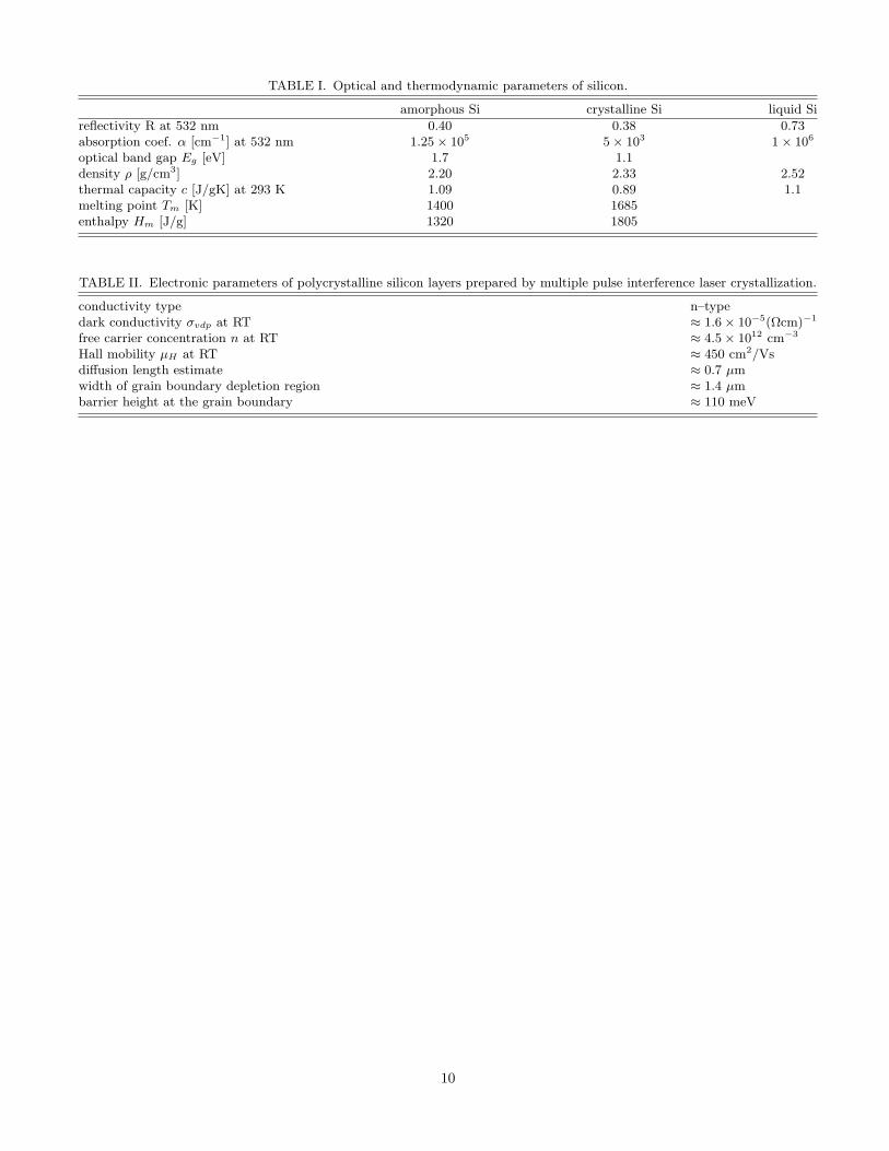
TABLE I. Optical and thermodynamic parameters of silicon.
amorphous Si crystalline Si liquid Si
reflectivity R at 532 nm 0.40 0.38 0.73absorption coef. α [cm−1] at 532 nm 1.25× 10⁵ 5× 10³ 1× 10⁶
optical band gap Eg [eV] 1.7 1.1density ρ [g/cm3] 2.20 2.33 2.52thermal capacity c [J/gK] at 293 K 1.09 0.89 1.1melting point Tm [K] 1400 1685enthalpy Hm [J/g] 1320 1805
TABLE II. Electronic parameters of polycrystalline silicon layers prepared by multiple pulse interference laser crystallization.
conductivity type n–typedark conductivity σvdp at RT ≈ 1.6× 10⁻⁵(Ωcm)−1
free carrier concentration n at RT ≈ 4.5× 1012 cm−3
Hall mobility µH at RT ≈ 450 cm2/Vsdiffusion length estimate ≈ 0.7 µmwidth of grain boundary depletion region ≈ 1.4 µmbarrier height at the grain boundary ≈ 110 meV
10

Fig. 1, Rezek
crystallizationthreshold
¯
growth
mc-Simc-Si a-Sia-Si
substrate
(c)
(a) laser beam interference
x
I
(b) periodic intensity profile

Nd:YAGlaser
beamsplitter
piezotable
sample
mirrors
Fig. 2, Rezek

Fig. 3, Rezek
solid
supercooled
SLG SLG
spontaneousnucleation
0 1 2 3 4 50
100
200
300
400
500
600
700
800
900
C
B
A
distance [mm]
inte
nsity
[mJ/
cm2 ]

1 pulsest
nd2 pulse
result
shift
Fig. 4, Rezek

Fig. 5, Rezek

Fig. 6, Rezek

4.5 mm
(a)
(b)
(c)
Fig. 7, Rezek

Fig. 8, Rezek
mm]
0 1 2 3 4 5 6 7
-40
-20
0
20
40
60
80
100
120
(1)
(2)
(3)
distance[mm]
secco 100 nm
±15%
(a) LBIC & AFM profiles
rela
tive
he
igh
t[n
m]
0.5 1.0 1.5 2.0 2.5
0
5
10
15
(b) FFT of LBIC & AFM profiles
frequency [1/
am
plit
ud
e [n
m]
0.0
0.1
0.2
0.3
0.4 0.40
1.06
am
plit
ud
e [p
A]
100 nm
±18%
8 9 10 11 0
1
2
3
4
5
6
7 5.5 pA ±16%
ph
oto
curr
en
t [p
A]
3.0 3.5 4.0
LBIC
AFM AFM, secco

(b)
(a)
I
x
p = 5.3 mm
AFM and LBIC scan direction
Fig. 9, Rezek

Fig. 10, Rezek
distance [mm]
ph
oto
curr
en
t [p
A]
ph
ase
sh
ift [d
eg
]
(a) LBIC spatial profile
period
0 2 4 6 8 10 12 14 16 18 20-15
-10
-5
0
5
10
15
20
25(b) AFM profile
distance [mm]
rela
tive
he
igh
t [n
m]
period
0 2 4 6 8 10 12 14 16 18 200.0
0.2
0.4
0.6
0.8
1.0
-180
-150
-120
-90
-60
-30
0
30
60
90
120
150
180

Fig. 11, Rezek
grain boundary
0°
- 180°
grain boundary
phase
amplitude
photocurrent
energybands

space charge
defects
+
--
-
--
-
++
EF
recombination(trapped electrons)
diffusion
drift
traps refilled
e-
e-
e-
h+
h+
e-
(a) (b)
Fig. 12, Rezek