Boron nitride,cubic boron nitride,hexagonal boron nitride nanopowders

1
BORON ACTIVATION AND DIFFUSION IN POLYCRYSTALLINE SILICON WITH FLASH-ASSIST RAPID THERMAL ANNEALING
By
SIDAN JIN
A DISSERTATION PRESENTED TO THE GRADUATE SCHOOL OF THE UNIVERSITY OF FLORIDA IN PARTIAL FULFILLMENT
OF THE REQUIREMENTS FOR THE DEGREE OF DOCTOR OF PHILOSOPHY
UNIVERSITY OF FLORIDA
2011

2
© 2011 Sidan Jin

3
To my family, for their endless support and encouragement
4
ACKNOWLEDGMENTS
I would like to acknowledge the members of the SWAMP research group, both
former and current. Each has been helpful in immeasurable ways. I would like to
specifically thank Nick Rudawski and Saurabh Morarka for their contributions. I would
also like to acknowledge my industrial liaisons at IBM, such as Paul Ronsheim and
Michael Hatzistergos for taking so much of their valuable time to help me with my
research. I would like to specifically mention former SWAMP member Renata Camillo-
Castillo for her dedication to providing me with the material in order to do this research.
Finally, I would like to acknowledge my advisor Kevin Jones and co-advisor Mark Law
for their immense knowledge, time, and jovial personalities while getting me through my
Ph.D.

5
TABLE OF CONTENTS
page
ACKNOWLEDGMENTS...................................................................................................4
TABLE OF CONTENTS ...................................................................................................5
LIST OF TABLES .............................................................................................................7
LIST OF FIGURES...........................................................................................................8
LIST OF ABBREVIATIONS............................................................................................11
CHAPTER
1 MOTIVATION...........................................................................................................15
1.1 Introduction ........................................................................................................15 1.2 Improving the Heterojunction Bipolar Transistor ................................................16 1.3 Objectives and Statement of Thesis ..................................................................17
2 LITERATURE SURVEY...........................................................................................18
2.1 Doping in Poly-Si ...............................................................................................18 2.1.1 In-situ doping ............................................................................................18 2.1.2 Ion implantation ........................................................................................19
2.2 Diffusion of Boron in Silicon ...............................................................................21 2.2.1 B diffusion and point defects ....................................................................22 2.2.2 B diffusion in polycrystalline Si .................................................................24
2.3 Flash-Assist Rapid Thermal Annealing..............................................................26 2.4 Electrical Properties of Poly-Si...........................................................................27
3 ANALYTICAL TECHNIQUES ..................................................................................35
3.1 Four Point Probe................................................................................................35 3.2 Hall Effect...........................................................................................................36 3.3 Secondary Ion Mass Spectrometry....................................................................39 3.4 3D Atom Probe Tomography .............................................................................40 3.5 Transmission Electron Microscopy ....................................................................43
4 GRAIN GROWTH IN B-DOPED POLY-SI ...............................................................51
4.1 Thermodynamics of Grain Growth .....................................................................51 4.2 Experimental Conditions ....................................................................................53 4.3 Results and Discussion......................................................................................54
5 MOBILITY, ACTIVATION, AND DEACTIVATION OF B-DOPED POLYSILICON WITH FLASH ANNEALING .....................................................................................62

6
5.1 Poly-Si in HBT Technology ................................................................................62 5.2 Experimental Methods .......................................................................................64 5.3 Electrical Activation and Mobility........................................................................65 5.4 Electrical Deactivation and Mobility ...................................................................69 5.5 Summary............................................................................................................72
6 B SEGREGATION TO GRAIN BOUNDARIES AND DIFFUSION IN POLYCRYSTALLINE SI WITH FLASH ANNEALING..............................................80
6.1 Importance of Dopant Segregation ....................................................................80 6.2 Experimental Methods .......................................................................................81 6.3 Results ...............................................................................................................82 6.4 Discussion..........................................................................................................88
7 APPLICATION OF 3D ATOM PROBE TOMOGRAPHY TO ANALYSIS OF FIELD EFFECT TRANSISTORS ON SILICON-ON-INSULATOR SUBSTRATES ..92
7.1 Challenges for 3D Analysis of SOI.....................................................................92 7.2 Methodology ......................................................................................................93 7.3 Results and Discussion......................................................................................95
8 CONCLUSIONS AND FUTURE WORK ................................................................102
APPENDIX
A FLOOPS SIMULATION CODE FOR B DIFFUSION IN POLY-SI ..........................104
B FLOOPS SIMULATION CODE FOR 2D B DIFFUSION OF SOURCE DRAIN EXTENSION IN P-MOSFET ON SOI ....................................................................106
LIST OF REFERENCES ..............................................................................................108
BIOGRAPHICAL SKETCH...........................................................................................113
7
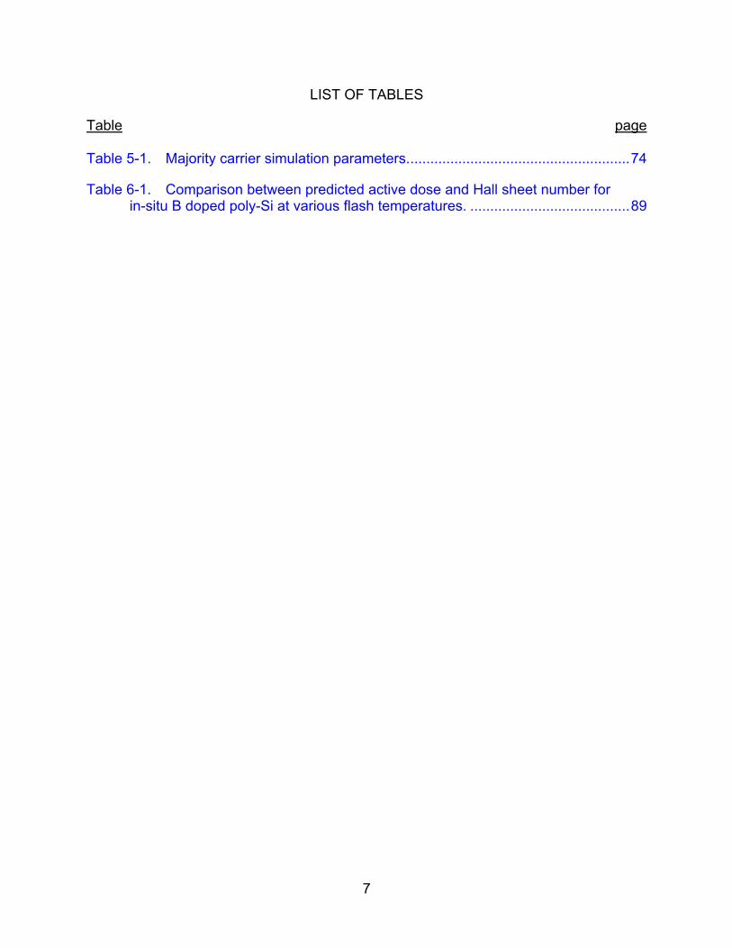
LIST OF TABLES
Table page Table 5-1. Majority carrier simulation parameters........................................................74
Table 6-1. Comparison between predicted active dose and Hall sheet number for in-situ B doped poly-Si at various flash temperatures. ........................................89
8
LIST OF FIGURES
Figure page Figure 2-1 Mattson Vortek Argon Arc Lamp ..............................................................31
Figure 2-2 Time-temperature profile comparison .......................................................31
Figure 2-3 Room temperature hole mobilities at various B doping concentrations in poly-Si57. ...............................................................................................32
Figure 2-4 Modeling grain boundary potential barrier ................................................33
Figure 2-5 Dependence of the potential barrier height on doping concentration .......34
Figure 2-6 Activation energy for overcoming the grain boundary energy barrier for various B doping concentrations...............................................................34
Figure 3-1 Schematic representation of four-point probe measurement. ..................47
Figure 3-2 Sample geometry for deriving sheet resistance from resistivity. ..............47
Figure 3-3 Illustration demonstrating the Hall voltage VH arising due to the Lorenz force from application of a magnetic field, B. ............................................47
Figure 3-4 Illustration of the van der Pauw Hall Effect geometry...............................48
Figure 3-5 Determining characteristic resistance RA and RB using van der Pauw technique. .................................................................................................48
Figure 3-6 Illustration of ion analysis from secondary ion mass spectrometry. .........49
Figure 3-7 Diagram demonstrating pulsed-laser assisted atom probe operation. .....49
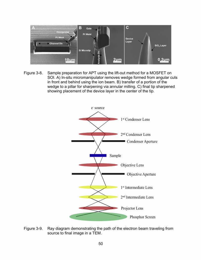
Figure 3-8 Sample preparation for APT using the lift-out method for a MOSFET on SOI.......................................................................................................50
Figure 3-9 Ray diagram demonstrating the path of the electron beam traveling from source to final image in a TEM.........................................................50
Figure 4-1 Cross-sectional transmission electron micrograph of poly-Si film.............57
Figure 4-2 SIMS profiles for initial B concentrations for as-deposited and with additional Ge+ and B+ implant ...................................................................57
Figure 4-3 Temperature profile for a 1350 °C flash anneal with a pre-flash temperature of 950 °C...............................................................................58
Figure 4-4 PTEM and grain size distribution for in-situ B doped poly-Si ....................59
9
Figure 4-5 PTEM and grain size distribution for Ge+ and B+ implanted poly-Si .........60
Figure 4-6 PTEM and grain size distribution for Ge+ and B+ implanted poly-Si using 950 °C pre-flash temperature (iRTP)...............................................61
Figure 4-7 Average grain sizes for in-situ doped and additionally implanted poly-Si with flash annealing. .............................................................................61
Figure 5-1 Schematic showing elevated extrinsic base for a heterojunction bipolar transistor ...................................................................................................74
Figure 5-2 SIMS profile comparison for initial B concentrations for as-deposited and with additional Ge+ and B+ implant.....................................................75
Figure 5-3 Sheet resistance comparison between as-deposited in-situ doped and additionally B implanted poly-Si films at various flash anneal conditions..................................................................................................75
Figure 5-4 Comparison of mobility values between flash-only and RTA + flash anneals .....................................................................................................76
Figure 5-5 Active sheet number measurements ........................................................76
Figure 5-6 Sheet number for 850 °C iRTP flash anneals compared with RTA anneals. ....................................................................................................77
Figure 5-7 B activation in crystalline Si from flash annealing of a 1 kV B implant to a dose of 1×1015 cm-2, and 30 kV Ge PAI .................................................77
Figure 5-8 Sheet resistance as a function of furnace annealing temperature following 1350°C flash anneal ...................................................................78
Figure 5-9 B deactivation measurements. .................................................................78
Figure 5-10 Hall measured mobility values for 30 min furnace anneals following flash anneals.............................................................................................79
Figure 5-11 Hole mobility behavior as a function of grain size from flash annealing ...79
Figure 6-1 B concentration profiles ............................................................................89
Figure 6-2 3D atom probe reconstruction using volume rendering ............................90
Figure 6-3 1-D concentration profile across the grain boundary.. ..............................90
Figure 6-4 pseg values from atom probe tomography .................................................91
Figure 6-5 An example of the diffusion model for a 1350°C flash anneal on an in-situ doped sample.....................................................................................91

10
Figure 7-1 Schematic representation comparing two different methods of APT sample orientation of FETs on SOI substrates..........................................98
Figure 7-2 XTEM micrograph of the p-FET structure..................................................98
Figure 7-3 SEM micrographs of APT sample preparation via FIB milling...................99
Figure 7-4 3D Reconstruction of as-implanted p-FET ................................................99
Figure 7-5 1D B concentration profiles across the gate SiO2 region of p-FETs after annealing at 900 °C as measured by APT ......................................100
Figure 7-6 Simulated concentration profile for interstitials generated from Xe+ ion implantation. ............................................................................................101
Figure 7-7 2D concentration map extracted from atom probe reconstruction for a 900 °C 16s anneal ...................................................................................101

11
LIST OF ABBREVIATIONS
APT Atom probe tomography
BIC Boron interstitial cluster
BiCMOS Bipolar CMOS
CMOS Complementary Metal-oxide-semiconductor
c-Si Crystalline silicon
CVD Chemical vapor deposition
FIB Focused ion beam
FIM Field-ion microscopy
fRTP Flash-assist rapid thermal processing
iRTP Impulse rapid thermal processing
HBT Heterojunction bipolar transistor
LEAP Local electrode atom probe
MOSFET Metal-oxide-semiconductor field-effect transistor
PFET p-type field-effect transistor
Poly-Si Polysilicon, or polycrystalline silicon
PTEM Plan-view transmission electron microscopy
RTA Rapid thermal annealing
SEM Scanning electron microscopy
SIMS Secondary ion mass spectrometry
SPER Solid phase epitaxial regrowth
SOI Silicon-on-insulator
TED Transient enhanced diffusion
TEM Transmission electron microscopy
TOF Time-of-flight

12
XTEM Cross-sectional transmission electron microscopy

13
Abstract of Dissertation Presented to the Graduate School of the University of Florida in Partial Fulfillment of the Requirements for the Degree of Doctor of Philosophy
BORON ACTIVATION AND DIFFUSION IN POLYCRYSTALLINE SILICON WITH
FLASH-ASSIST RAPID THERMAL ANNEALING
By
Sidan Jin
December 2011
Chair: Kevin S. Jones Major: Materials Science and Engineering
The rigorous scaling in dimensions for future generations of transistor fabrication
demands ever steeper requirements for dopant solubility with minimal diffusion.
Advanced annealing techniques such as flash-assist rapid thermal processing now
allow effective anneal times up to three orders of magnitude less than conventional
methods. At the same time, advanced characterization techniques can now provide
three-dimensional compositional analysis of materials systems. While there has been
extensive research for flash annealing of B doped crystalline Si, the effects on
polycrystalline Si have been less studied, but is of equal importance. It continues to be
prevalent in device fabrication for current and future technologies.
The morphology and evolution of grains in heavily B-doped poly-Si is studied
under high temperature millisecond annealing conditions using plan-view transmission
electron microscopy. High activation with low thermal budgets has allowed study of a
very fine-grained microstructure of highly activated B doped poly-Si. 3D atom probe
tomography allowed direct quantitative measurement of the segregation coefficient of B
to the grain boundaries, and its diffusion behavior has been accurately modeled.
Activation, mobility, and deactivation of B in flash annealed polycrystalline Si was also

14
explored using Hall effect. By combining electrical, compositional and microstructural
measurements, a model has been developed to describe the activation, mobility, and
diffusion behavior of B in poly-Si films with average hole concentrations greater than
5×1019 cm-3.
15
CHAPTER 1 MOTIVATION
The semiconductor industry has seen tremendous innovation over the past half-
century as it attempts to keep pace with Moore’s Law; the observation and prediction of
transistor density growth by Intel co-founder Gordon Moore, who stated that the number
of transistors on a chip would double each year1. In an attempt to fulfill Moore’s Law, the
industry has managed to double transistor density at a pace of roughly every 18-24
months. As transistor dimensions scale well into the nanometer and even angstrom
level, suppressing diffusion has required incredible innovation in thermal processes.
The effects of these advanced thermal processes on electrical properties and diffusion
in polycrystalline Si, a widely used material for transistor fabrication, must be explored.
1.1 Introduction
Silicon (Si) is the second most abundant element in the Earth’s crust2, making up
roughly one-fourth of its total weight. Due to its relatively low cost as a semiconductor, it
has been the primary material used in the fabrication of devices for integrated circuits3
(IC) as well as photovoltaics4.
Like many solid materials at room temperature, Si can exist in a single crystalline
(c-Si) or polycrystalline form (poly-Si). For electronics applications, the Si is processed
to ultra high purities and formed into a single-crystalline state. Oftentimes, processing
conditions do not allow the deposition of single-crystalline Si due to lack of a crystalline
“seed” surface to grow epitaxially from. In such a case, poly-Si must be used instead.
Since the primary difference between c-Si and poly-Si is the presence of grain
boundaries, it is important to understand the effect these boundaries have on the
material system. Furthermore, due to aggressive scaling in integrated circuits, variability
16
and device yield become of increasingly greater concern when grain sizes and device
dimensions become comparable. Therefore, it is pertinent to understand the role of
grain boundaries in polysilicon as it pertains to current and next-generation processing
conditions in integrated circuits.
1.2 Improving the Heterojunction Bipolar Transistor
Oftentimes in device fabrication processing, use of single-crystalline silicon for
some structures is simply unfeasible due to the lack of a crystalline surface to act as a
seed for epitaxy5, 6. One such example is in the case of high-performance SiGe:C
heterojunction bipolar transistors, where poly-Si forms the elevated extrinsic base in the
base layer of the structure and is deposited over oxide5. Improving the transit frequency,
fT, and the maximum oscillation frequency, fMAX, has proven to be challenging due to
compensating effects for a given thermal budget. A low thermal budget aids in
delivering the highest transit frequencies due to reduced diffusion in the base, thereby
allowing a thin base width7. However, because of increased base resistance due to
lower activation using a low thermal budget, fmax is reduced.
With this in mind, the application of millisecond annealing using flash-assist rapid
thermal processing (fRTP) to B-doped poly-Si presents itself very favorably7, 8. High
temperature annealing (up to 1350°C) allows greater B solubility9, and therefore lower
resistance, while short annealing timescales significantly limits diffusion8. The typical
pulse width10 for flash annealing is on the order of 1 ms. While the scope of this
research focuses on the electrical properties of poly-Si in its application as the elevated
extrinsic base in bipolar CMOS technology5, the results presented form a fundamental
basis for understanding the effect of millisecond annealing on sheet resistance,
activation, and mobility of heavily B-doped poly-Si films. This is then verified with
17
microstructural and compositional analysis using three-dimensional analytical
techniques.
1.3 Objectives and Statement of Thesis
The goal of this work is to explore the effect of millisecond annealing on the
electrical and chemical properties of B doped poly-Si. The low thermal budgets allowed
by using flash-assist rapid thermal processing (fRTP) explores a new regime in
microstructure and dopant activation—specifically suppressed grain growth with very
high levels of dopant activation.
The results of this research have provided a number of scientific contributions.
Using transmission electron microscopy, the mechanism for grain growth in heavily B
doped poly-Si films under flash annealing has been verified to be of lattice dislocation
motion. Activation, mobility, and deactivation measurements using Hall effect of heavily
B doped poly-Si films with flash annealing up to 1350 °C led to creation of a
mathematical model relating grain size, activation, and mobility for hole concentrations
greater than 5×1019 cm-3. A model was also developed for quantitative values for grain
boundary segregation of B, which was previously thought to not occur. This was
achieved by using flash annealing to create a highly activated yet very fine
microstructure of poly-Si. This fine microstructure allowed for direct evidence of B
segregation using 3D atom probe tomography, a powerful analytical technique with a
limited field of view. The measured segregation data then allowed for accurate
simulation of B diffusion through the polycrystalline film. Finally, the work has been able
to apply 3D atom probe tomography to commercially fabricated field-effect transistor
devices, revealing B segregation to the gate oxide and verification of surface
recombination velocity of point defects.
18
CHAPTER 2 LITERATURE SURVEY
2.1 Doping in Poly-Si
The fundamental property of a semiconductor is its ability to behave as both an
insulator and a conductor depending on the impurities that are added11. For Si, the most
common p-type dopant is B. Doping is typically incorporated into the material by two
processes. In-situ doping refers to incorporation of dopant either during crystal growth
or during deposition of material. Poly-Si is typically deposited from a gas-phase source
using chemical vapor deposition (CVD). Dopant atoms are typically incorporated
automatically into the lattice using this method up to a certain concentration. Another
method of introducing dopant atoms into Si is via ion implantation, where dopant atoms
are ionized and accelerated under a high potential and forced into the substrate
material. This process causes significant damage to the crystalline lattice and an
annealing step is required to repair the damage and incorporate the dopant atoms onto
substitutional lattice positions in order to contribute to conduction. The thermal
treatment gives rise to diffusion, and so annealing techniques such as flash annealing
have been developed in order to reduce the effective time of the anneal.
2.1.1 In-situ doping
Poly-Si is typically deposited in a low-pressure chemical vapor deposition
chamber, with the decomposition of silane (SiH4) via the reaction12
SiH4 (g)→SiH4 (s)→Si(s) + 2H2 (2-1)
Low-pressure deposition reduces unwanted gas phase reactions as well as
improves film uniformity. Doping the films with B involves addition of diborane gas
(B2H6) to silane during deposition. First, diborane undergoes thermal decomposition
19
B2H6(g)→2BH3(g) (2-2)
The actual incorporation of B into Si is thought to proceed by13
BH3(g)→BH3(s)→B(s) + (3/2)H2 (2-3)
The amount of B incorporation has been seen to depend linearly with diborane/silane
ratio14.
An advantage for n-situ doping is that it allows for direct incorporation of B into
the crystal lattice, thereby removing the need for an annealing step in order to activate
the dopant onto a lattice position. However, for poly-Si the activation is not complete
due to some amount of dopant in an inactive state at the grain boundaries. Varying the
diborane/silane ratio has also been shown to effect the microstructure of the as-
deposited film15.
2.1.2 Ion implantation
Ion Implantation is the most common method of doping for integrated circuit
technology. The technique involves accelerating dopant ions under an electric field and
implanting them directly into the semiconductor substrate. The process allows for very
good control, precision, uniformity, and repeatability, however, the crystal suffers
significant radiation damage16, which must be repaired by way of an annealing step.
There are two stopping mechanisms for which the accelerated ion comes to rest
within the material. The first is called nuclear stopping, which represents elastic
collisions between the ions and the recoiled atoms of the lattice. The second, termed
electronic stopping, describes the electrostatic interactions between the ions and the
outer shell electrons of the semiconductor.

20
Nuclear stopping is a process that creates Frenkel pair defects. A Frenkel pair
describes a pair of point defects created when a Si atom is displaced into an interstitial
position and the vacancy it left behind. Collisions are elastic and require a conservation
of momentum. 15 eV of energy is required to displace an atom of Si off of its lattice
position. The amount of damage is therefore a function of incoming ion energy, the ion’s
mass, implanter current, and substrate temperature.
The sum total of energy loss by nuclear and electronic stopping determines the
range the ion travels within the material. The ion distribution is of a Gaussian shape,
with a projected range Rp and a straggle ΔRp.
2.1.2.1 Amorphization
Beyond a critical damage density17, 18, the Si crystal undergoes a first order phase
transformation into an amorphous phase19. The minimum ion dose necessary to induce
amorphization is dependent on the ion’s mass, its energy, dose rate, and the
temperature of the substrate20.
2.1.2.2 Activation via solid phase regrowth
In Si, one way to increase activation of dopant is to first create an amorphous layer
and implant the dopant into it. Implantation into the amorphous phase and subsequent
annealing allows the crystal to repair from the underlying seed and incorporate the
dopant into the lattice during this regrowth, termed solid phase epitaxial regrowth
(SPER)21-23. This allows much higher solubility, and thereby activation, than equilibrium
solubility since regrowth can occur at relatively low annealing temperatures.
Preamorphization and regrowth can similarly be applied to a polycrystalline
structure. It has been shown that the regrowth rate varies significantly for different
crystallographic orientations24 and so in a polycrystalline structure, the growth of the
21
amorphous-crystalline interface can be very rough, with some areas showing full
regrowth while others exhibiting very little. It has also been shown that at sufficiently
high implantation doses, c-Si regrows as poly-Si25.
One of the drawbacks to the preamorphization and regrowth process is the
generation of excess interstitials from the implantation process, which manifest
themselves as end-of-range (EOR) defects16, 26 at a distance slightly beyond the
amorphous-crystalline interface. The dissolution kinetics of EOR defects releases
interstitials and creates a supersaturated environment, which significantly enhances B
diffusion27, 28.
2.2 Diffusion of Boron in Silicon
A consequence of the thermal processes in microelectronics fabrication is diffusion
of B through the material. For poly-Si, this can be very rapid due to the enhanced
diffusivity of B in the grain boundaries29, 30. In order to understand diffusion of B in poly-
Si one must first understand the mechanisms for B diffusion in single crystalline silicon
(c-Si), and before that, one must first understand the basic concept of diffusion.
Thermodynamically, the process of diffusion is driven by the gradient of the
concentration profile, or more specifically, the reduction of the gradient in chemical
potential. For ideal mixtures, these are equivalent. At its most fundamental level, the
driving force is simply an availability of sites as atoms diffuse in the lattice by random
walk. Areas with low concentrations of dopant atoms have more available sites to
occupy, and so there is a net motion of atoms from higher concentration to lower
concentration.
In the case of B doped Si, this flux, J, of B from high concentration to low
concentration can be described by Fick’s 1st law in one-dimension by,

22
J = −D∂C∂x
(2-4)
where D represents the diffusivity in dimensions of length2 per time, such as cm2/s, and
C is the concentration. In order to predict how the diffusion changes with respect to
time, Fick’s 2nd law can be derived from Fick’s first law using mass balance,
∂C∂t
= −∂∂xJ =
∂∂x
D ∂∂xC
⎛
⎝ ⎜
⎞
⎠ ⎟ = D
∂ 2C∂x
(2-5)
The diffusivity, D, can be described by the Arrhenius expression
D = D0 exp−Ea
kT⎛
⎝ ⎜
⎞
⎠ ⎟ (2-6)
where D0 is the pre-exponential factor, Ea is the activation energy, k is Boltzmann’s
constant, and T is the absolute temperature.
Unfortunately, diffusion of B in Si is not so simplistically behaved as to be a
function of only the concentration gradient. However, it has been well studied for a wide
range of concentrations and annealing conditions, and so can be built upon for
application to a polycrystalline microstructure under millisecond annealing conditions.
2.2.1 B diffusion and point defects
It is widely accepted that the mechanism for dopant diffusion in Si is governed by
the interactions between dopants and point defects such as interstitials and vacancies31.
The available reactions for B diffusion in Si can be described via the equations31
B + V BV (2-7)
B + I BI (2-8)
B + I Bi (2-9)
23
B Bi + V (2-10)
where V represents a Si vacancy and I represents a Si self-interstitial. Eq. (2-7)
describes diffusion via a vacancy mechanism, (2-8) by an interstitial mechanism, and
(2-9) by an interstitialcy kick-out mechanism. Eq. (2-10) describes a dissociative
reaction known as the Frank-Turnbull mechanism32 whereby a B atom on a
substitutional lattice position moves into an interstitial position, leaving behind a
vacancy. It is expected that in an environment of excess interstitials, Eq. (6) would
dominate, while conversely, Eq. (2-10) would apply in an environment of excess
vacancies.
It has been shown that B diffuses by almost a purely interstitialcy mechanism33,
where a Si self-interstitial supplants a substitutional B atom via a kick-out process, thus
allowing it to diffuse through the crystal. As the B atom later supplants a Si atom on the
lattice, a new Si interstitial is generated and the process repeats. The concentration for
interstitials can drastically increase above the equilibrium concentration due to many
processes, such as generation of Frenkel pairs from ion implantation27, 34, generation of
interstitials via oxidation of the surface35, and even release of interstitials from high
concentrations of Si-B clusters36. This supersaturation of interstitials relative to the
equilibrium concentration32, 37 of interstitials therefore represents an enhancement factor
to the diffusivity of B, and can be expressed by
DB = DB* CI
CI* (2-11)
where DB* represents the diffusivity of B at an equilibrium concentration of interstitials.
24
This supersaturation of interstitials represents a non-equilibrium system and so
there is a driving force to remove the excess interstitials. The diffusivity enhancement
has been termed transient enhanced diffusion28 (TED), referring to the time transient
required for the system to return to equilibrium, and the enhancement ratio CI/CI* to
return to unity. For ion implantation processes, this time transient arises due to the
formation of extended defects, primarily {311} rod-like defects16 whose dissolution
kinetics release a steady stream of interstitials into the system27. Excess interstitials
typically diffuse to and annihilate at the surface38-40, although they may recombine with
vacancies or form boron-interstitial clusters (BIC)41.
For a polycrystalline structure, the grain boundaries may be thought of as effective
surfaces for point defect recombination42. In fine-grained poly-Si structures, as is the
case when small thermal budgets such as flash annealing do not allow for significant
grain growth, the surface area available for recombination can be very high. The effect
of this environment will be explored when discussing diffusion of B in the polycrystalline
structure.
2.2.2 B diffusion in polycrystalline Si
It has been shown that grain boundaries in poly-Si act as an effective sink for
vacancies, and postulated that the same is true for interstitials43. Polycrystalline films of
CoSi2 deposited on Si have been shown to generate an interstitial undersaturation44. In
fine-grained poly-Si structures, as is the case when small thermal budgets such as flash
annealing do not allow for significant grain growth, the surface area available for
recombination can be very high, thus reducing enhanced diffusivity effects arising from
processes that create a supersaturation of interstitials discussed previously.
25
However, the presence of grain boundaries has a profound impact on diffusion in a
polycrystalline structure due to an enhancement in B diffusivity in the grain boundary29
that is several orders of magnitude greater than in the bulk. Dopants such as As and P
have been shown to segregate to grain boundaries in poly-Si45-48, but reports on B
segregation to the grain boundary are conflicting3, 45-47, 49, 50. Results seem to suggest
that segregation is only seen at very high concentrations (>1.3 at%) Nevertheless, it has
been demonstrated that diffusion of B in poly-Si is significantly faster than in bulk c-Si,
suggesting an enhanced diffusivity within or near the grain boundaries themselves.
The modeling aspect for this behavior45, 51-54 has been well studied for As and P.
Mathematically, the diffusion in a polycrystalline structure is described by splitting the
diffusion equations into diffusivity of the dopant within a crystallite (Di) and diffusivity of
the dopant within a grain boundary (Digb). The differential equations are
∂Cig
∂t=∂∂xDi∂Ci
g
∂x+τ −1 Ci
g pseg −Cigb( ) (2-12)
∂Cigb
∂t=∂∂xDi
gb ∂Cigb
∂x−τ −1 Ci
g pseg −Cigb( ) (2-13)
where the subscript i denotes the diffusing impurity species, and the segregation
coefficient, pseg = Cigb/Ci
g is maintained at steady state. The two concentrations are
coupled by a kinetic reaction term, where τ represents the rate of segregation. The
model describes diffusion in terms of a random walk, whereby if the dopant encounters
a grain boundary, it takes much larger steps due to the increased diffusivity, but may
also jump back into the grain. τ represents the rate for this process occuring, while pseg
describes the tendency for the diffusing atom to remain in the boundary.

26
In this work, this diffusion model is extended to B diffusion in poly-Si using direct
chemical analysis of B segregation to the grain boundaries. Flash annealing and heavy
doping create an ideal environment for B segregation. Prior work regarding dopant
segregation was mainly inferred from electrical measurements45, 53, and thus may not
accurately be able to detect low segregation at large grain sizes where its influence is
expected to be minimal on conduction.
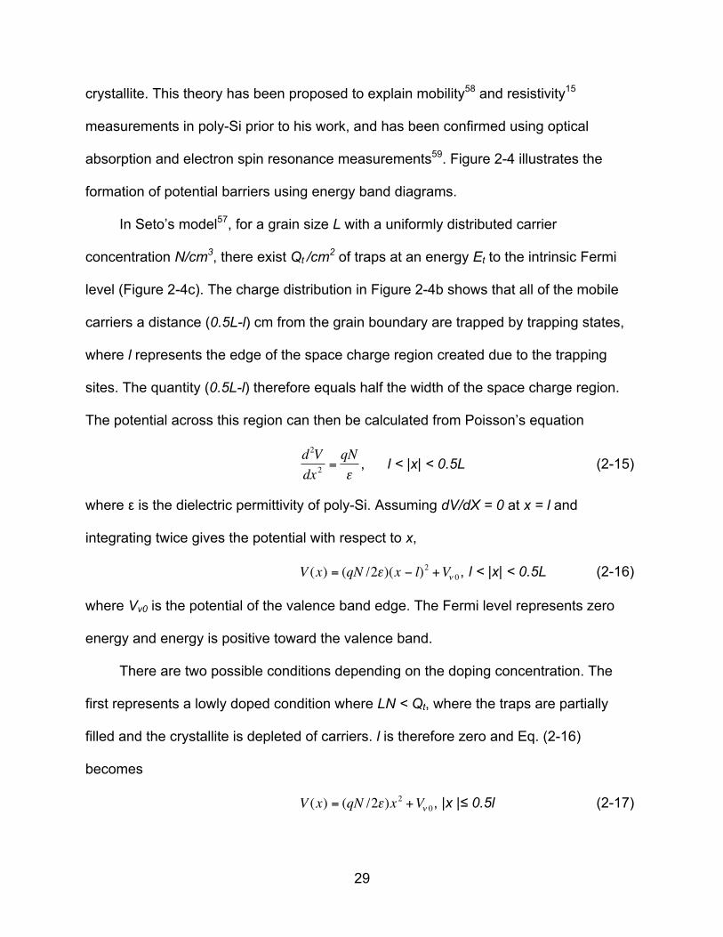
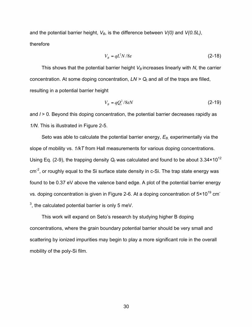
2.3 Flash-Assist Rapid Thermal Annealing
To meet future metrics for dopant activation and limited dopant diffusion, thermal
processing has evolved to ever increasing ramp-up and cooling rates in order to reduce
the effective annealing times at high temperatures. Conventional rapid thermal
processing (RTP) heats wafers by use of incandescent tungsten lamps to allow ramp
rates up to 350°C-s-1, however, this is no longer sufficient for the needs of future
technology nodes. In fact, it has been shown that heating rates beyond 100°C-s-1 give
no improvement with regard to diffusion55. This is due to the inability for conventional
RTP to minimize the soak and cooling times of the anneal.
Power, spectral distribution, and response time govern the performance for lamp-
based heating of Si. The use of an argon arc lamp allows much higher power and
response time than tungsten lamps. Tungsten lamps operate at 3500K, which
represents a power of 103 W. In contrast, the argon plasma in an arc lamp operates at
12000K, resulting in a power of 106 W, which allows four orders of magnitude
improvement in ramp rates over tungsten lamps. With regard to spectral distribution,
only 40% of the radiation generated from the tungsten lamp is below the band gap
absorption of Si, while over 95% of the radiation emitted from the arc lamp is
absorbed56. The thermal response time for the arc lamps is also roughly a magnitude
27
faster10 (25 ms vs. 300 ms) due to the smaller thermal mass of argon compared to
tungsten. This allows for a much faster transition from heating to cooling with the arc
lamp.
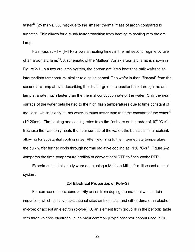
Flash-assist RTP (fRTP) allows annealing times in the millisecond regime by use
of an argon arc lamp10. A schematic of the Mattson Vortek argon arc lamp is shown in
Figure 2-1. In a two arc lamp system, the bottom arc lamp heats the bulk wafer to an
intermediate temperature, similar to a spike anneal. The wafer is then “flashed” from the
second arc lamp above, describing the discharge of a capacitor bank through the arc
lamp at a rate much faster than the thermal conduction rate of the wafer. Only the near
surface of the wafer gets heated to the high flash temperatures due to time constant of
the flash, which is only ~1 ms which is much faster than the time constant of the wafer10
(10-20ms). The heating and cooling rates from the flash are on the order of 106 °C-s-1.
Because the flash only heats the near surface of the wafer, the bulk acts as a heatsink
allowing for substantial cooling rates. After returning to the intermediate temperature,
the bulk wafer further cools through normal radiative cooling at ~150 °C-s-1. Figure 2-2
compares the time-temperature profiles of conventional RTP to flash-assist RTP.
Experiments in this study were done using a Mattson Millios™ millisecond anneal
system.
2.4 Electrical Properties of Poly-Si
For semiconductors, conductivity arises from doping the material with certain
impurities, which occupy substitutional sites on the lattice and either donate an electron
(n-type) or accept an electron (p-type). B, an element from group III in the periodic table
with three valence electrons, is the most common p-type acceptor dopant used in Si.

28
Conduction in p-type Si occurs via holes since the removal of an electron results in a
positively charged hole.
The conductivity of the semiconductor can be described by the equation
σ = qnµe + qpµh (2-14)
where q is the elementary charge of the electron (1.602×10⁻¹⁹ C), n and p represent
concentrations of electrons and holes, respectively, while µe and µh represent their
respective electron and hole mobilities. Even at low B doping levels (~1016 cm-3),
conduction via holes dominates and the impact from electron conduction can be ignored
since the intrinsic carrier concentration in Si at room temperature is only 1×1010 cm-3.
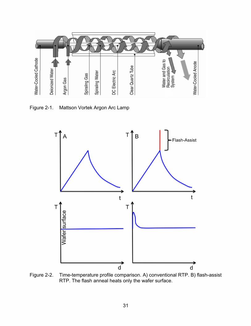
For both single crystalline Si (c-Si) and polycrystalline Si (poly-Si), the effect of
dopant concentration on resistivity is essentially the same. Greater concentrations of
carriers equate to lower resistance. In fact, at significantly high doping levels, the
resistivity of poly-Si is comparable to that of c-Si49. This is due to degradation in carrier
mobility for c-Si with increasing doping concentration due to increased scattering from
high concentrations of ionized impurities. While the mobility is overall less in poly-Si, it
has been seen to rise57, 58 with increasing doping concentration above 1018 cm-3. Figure
2-3 depicts the effects of doping concentration on carrier mobility for c-Si and poly-Si.
The presence of grain boundaries in poly-Si has a significant impact on the mobility of
carriers57, 58.
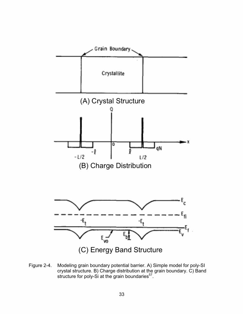
57Seto proposed a model to explain the measured Hall mobilities in poly-Si by
treating grain boundaries as trapping sites for carriers due to their disorder and
incomplete atomic bonding. This leads to accumulation of charge and formation of
potential barriers that carriers must surmount in order to move from crystallite to
29
crystallite. This theory has been proposed to explain mobility58 and resistivity15
measurements in poly-Si prior to his work, and has been confirmed using optical
absorption and electron spin resonance measurements59. Figure 2-4 illustrates the
formation of potential barriers using energy band diagrams.
In Seto’s model57, for a grain size L with a uniformly distributed carrier
concentration N/cm3, there exist Qt /cm2 of traps at an energy Et to the intrinsic Fermi
level (Figure 2-4c). The charge distribution in Figure 2-4b shows that all of the mobile
carriers a distance (0.5L-l) cm from the grain boundary are trapped by trapping states,
where l represents the edge of the space charge region created due to the trapping
sites. The quantity (0.5L-l) therefore equals half the width of the space charge region.
The potential across this region can then be calculated from Poisson’s equation
d2Vdx 2
=qNε
, l < |x| < 0.5L (2-15)
where ε is the dielectric permittivity of poly-Si. Assuming dV/dX = 0 at x = l and
integrating twice gives the potential with respect to x,
V (x) = (qN /2ε)(x − l)2 +Vν 0, l < |x| < 0.5L (2-16)
where Vv0 is the potential of the valence band edge. The Fermi level represents zero
energy and energy is positive toward the valence band.
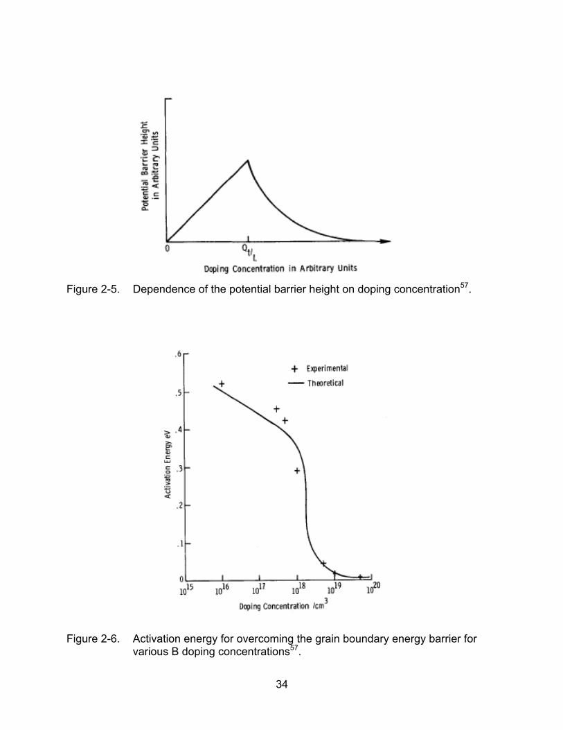
There are two possible conditions depending on the doping concentration. The
first represents a lowly doped condition where LN < Qt, where the traps are partially
filled and the crystallite is depleted of carriers. l is therefore zero and Eq. (2-16)
becomes
V (x) = (qN /2ε)x 2 +Vν 0, |x |≤ 0.5l (2-17)
30
and the potential barrier height, VB, is the difference between V(0) and V(0.5L),
therefore
VB = qL2N /8ε (2-18)
This shows that the potential barrier height VB increases linearly with N, the carrier
concentration. At some doping concentration, LN > Qt and all of the traps are filled,
resulting in a potential barrier height
VB = qQt2 /8εN (2-19)
and l > 0. Beyond this doping concentration, the potential barrier decreases rapidly as
1/N. This is illustrated in Figure 2-5.
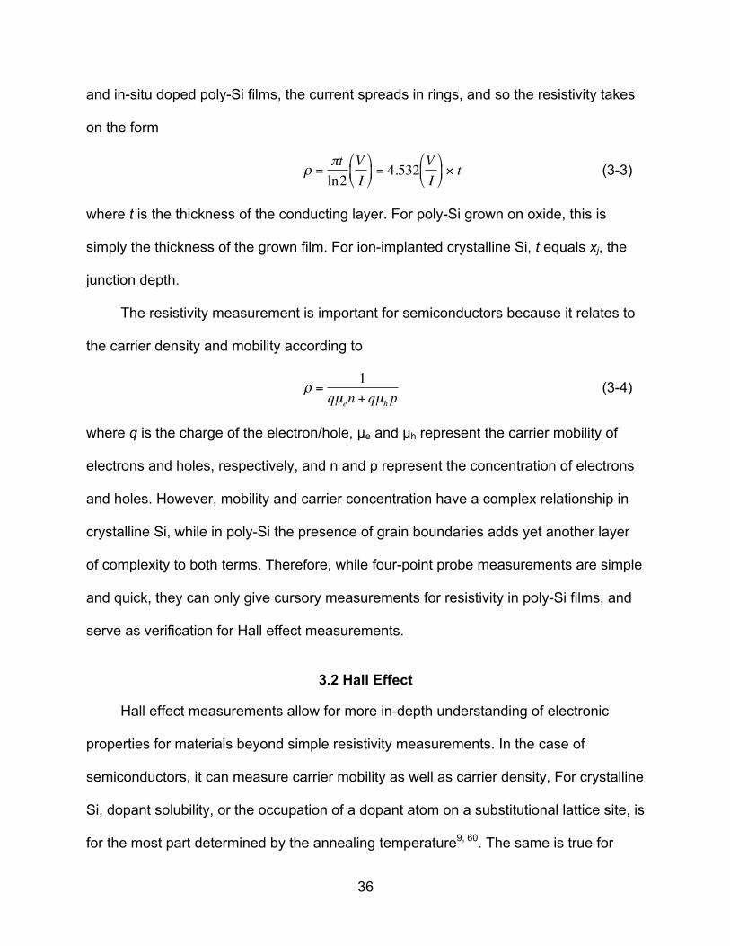
Seto was able to calculate the potential barrier energy, EB, experimentally via the
slope of mobility vs. 1/kT from Hall measurements for various doping concentrations.
Using Eq. (2-9), the trapping density Qt was calculated and found to be about 3.34×10¹²
cm-2, or roughly equal to the Si surface state density in c-Si. The trap state energy was
found to be 0.37 eV above the valence band edge. A plot of the potential barrier energy
vs. doping concentration is given in Figure 2-6. At a doping concentration of 5×1019 cm-
3, the calculated potential barrier is only 5 meV.
This work will expand on Seto’s research by studying higher B doping
concentrations, where the grain boundary potential barrier should be very small and
scattering by ionized impurities may begin to play a more significant role in the overall
mobility of the poly-Si film.
31
Figure 2-1. Mattson Vortek Argon Arc Lamp
Figure 2-2. Time-temperature profile comparison. A) conventional RTP. B) flash-assist
RTP. The flash anneal heats only the wafer surface.
32
Figure 2-3. Room temperature hole mobilities at various B doping concentrations in
poly-Si57.
33
Figure 2-4. Modeling grain boundary potential barrier. A) Simple model for poly-SI
crystal structure. B) Charge distribution at the grain boundary. C) Band structure for poly-Si at the grain boundaries57.
34
Figure 2-5. Dependence of the potential barrier height on doping concentration57.
Figure 2-6. Activation energy for overcoming the grain boundary energy barrier for
various B doping concentrations57.

35
CHAPTER 3 ANALYTICAL TECHNIQUES
This chapter details the various analytical techniques used in this work. It serves to
educate the reader with some basic background knowledge of the capabilities and
limitations of each technique, so as to better interpret the results.
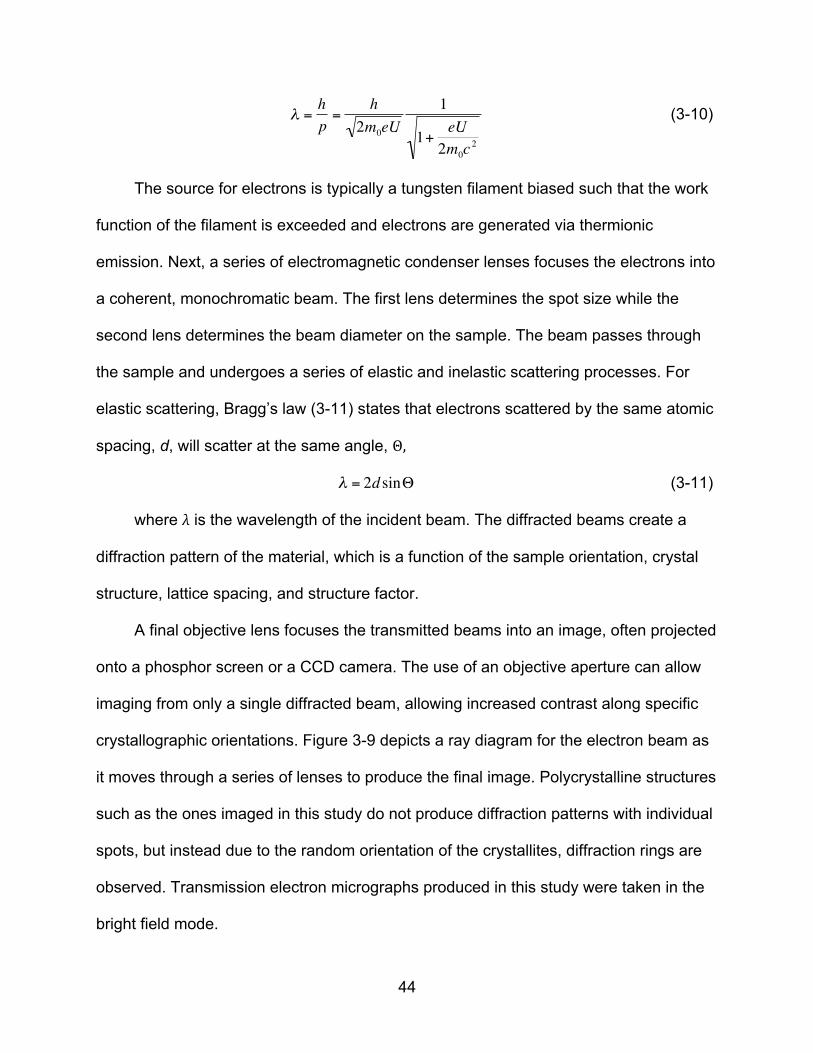
3.1 Four Point Probe
The Four Point Probe, as suggested by its name, uses four probes to measure
resistivity in a material. A schematic for the probes is given in Figure 3-1. A current is
supplied through the outer probes (1-4) and a voltage drop is measured through the
inner probes. By measuring the voltage drop through the inner probes (2-3), the
resistance of the outside probes themselves can be neglected since practically no
current flows through the inner probes.
For a cubic three-dimensional conductor with length l, and cross sectional area A,
(Figure 3-2) the resistance can be described as the resistivity multiplied by the length
and divided by the cross-sectional area. By grouping the resistivity with the thickness of
the sample, a sheet resistance RS allows description of resistivity in terms of “squares”
(l=w). The unit for RS is ohms, however, it is commonly referred to as ohms/square.
R =ρlA
=ρt
⎛
⎝ ⎜ ⎞
⎠ ⎟ lw
= RSlw
(3-1)
For probes of uniform spacing s, the resistivity can be described as,
ρ = 2πs VI
⎛
⎝ ⎜
⎞
⎠ ⎟ (3-2)
where the current emanates from the probe tips in a spherical fashion. If the conducting
layer is very thin compared to the probe spacing, as is typical for ion implanted layers
36
and in-situ doped poly-Si films, the current spreads in rings, and so the resistivity takes
on the form
ρ =πtln2
VI
⎛
⎝ ⎜
⎞
⎠ ⎟ = 4.532
VI
⎛
⎝ ⎜
⎞
⎠ ⎟ × t (3-3)
where t is the thickness of the conducting layer. For poly-Si grown on oxide, this is
simply the thickness of the grown film. For ion-implanted crystalline Si, t equals xj, the
junction depth.
The resistivity measurement is important for semiconductors because it relates to
the carrier density and mobility according to
ρ =1
qµen + qµh p (3-4)
where q is the charge of the electron/hole, µe and µh represent the carrier mobility of
electrons and holes, respectively, and n and p represent the concentration of electrons
and holes. However, mobility and carrier concentration have a complex relationship in
crystalline Si, while in poly-Si the presence of grain boundaries adds yet another layer
of complexity to both terms. Therefore, while four-point probe measurements are simple
and quick, they can only give cursory measurements for resistivity in poly-Si films, and
serve as verification for Hall effect measurements.
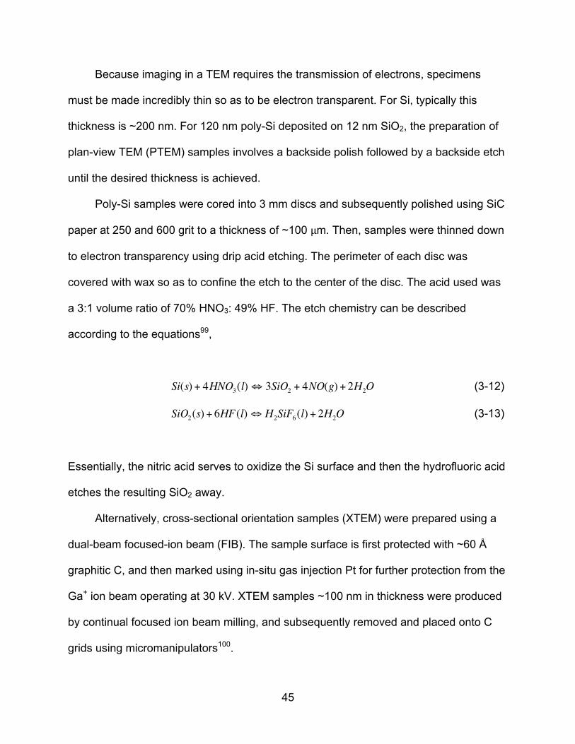
3.2 Hall Effect
Hall effect measurements allow for more in-depth understanding of electronic
properties for materials beyond simple resistivity measurements. In the case of
semiconductors, it can measure carrier mobility as well as carrier density, For crystalline
Si, dopant solubility, or the occupation of a dopant atom on a substitutional lattice site, is
for the most part determined by the annealing temperature9, 60. The same is true for
37
poly-Si, however, the presence of grain boundaries adds a further layer of complexity by
allowing energetically favorable sites for dopant segregation45, which lead to potential
barriers that impede carrier mobility57.
The Hall effect arises when a magnetic field is applied perpendicular to a moving
carrier. The field causes a deflection in the moving carrier that is perpendicular to both
the magnetic field and the plane the carrier was traveling in. This deflection is produced
by the Lorenz force11, and introduces a potential difference across the sample resulting
in an electric field. This is depicted in Figure 3-3 using an electron as the carrier. This
potential difference is known as the Hall voltage, VH. In semiconductors, both electrons
and holes deflect to the same side of the sample due to opposite charges as well as
opposite velocities.
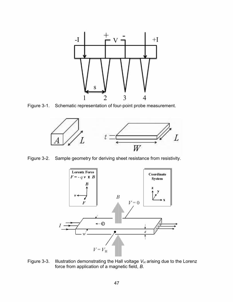
Measurement of the Hall voltage is done using the van der Pauw technique61, 62
illustrated in Figure 3-4. A constant current is forced through opposing contacts (1-3)
and the Hall voltage is measured across (2-4). The magnitude of the Hall voltage, VH,
relates to both the current traveling through the sample and the applied field through the
relation
VH =IBqnS
(3-5)
where q is the elementary charge of the carrier (1.602×10-‐19 C), I is the current applied, B
is the magnitude of the magnetic field, and ns is the sheet density of the carriers. For the
experiments conducted here, a constant current of 1.0 mA is applied across the sample
while the Hall voltage is measured and averaged for both positive and negative
magnetic fields at 0.4 T, 0.7 T, and 1.0 T.

38
The Hall voltage then allows determination of the sheet number, nS, which allows
for calculation of the mobility, μ, through the relation
µ =1
qnSRS (3-6)
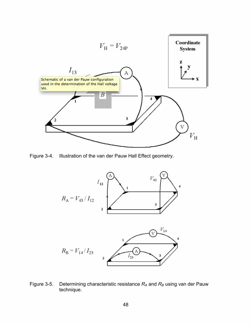
Calculation for sheet resistance, RS, can also be accomplished using the van der
Pauw technique through the relation,
exp nRA
RS
⎛
⎝ ⎜
⎞
⎠ ⎟ + exp
nRB
RS
⎛
⎝ ⎜
⎞
⎠ ⎟ =1 (3-7)
where RA and RB are characteristic resistances determined from measurements
according to Figure 3-5. For p-type semiconductors, where p represents the active hole
concentration, the Hall coefficient is defined as
RH =1qp
(3-8)
Due to the complex energy band structure of the material giving rise to changes in
effective mass of holes, as well as lattice scattering, and ionized impurity scattering63,
correction factors need to be applied to Hall effect measurements in order to obtain
accurate mobilities and sheet numbers63, 64. This correction factor is known as the Hall
factor, r, and relates to the Hall coefficient, RH, by
RH =rqp
(3-9)
Therefore, active doses must be multiplied by the Hall factor, r, while Hall mobility must
be divided by r to determine the true conductivity mobility. 63For hole concentrations
above 1×1020 cm-3, which represents all of the material in this work, the Hall factor used
is 0.7.
39
Measurements for this study were done using a Lakeshore 7507 Hall Effect
system at 20 °C.
3.3 Secondary Ion Mass Spectrometry
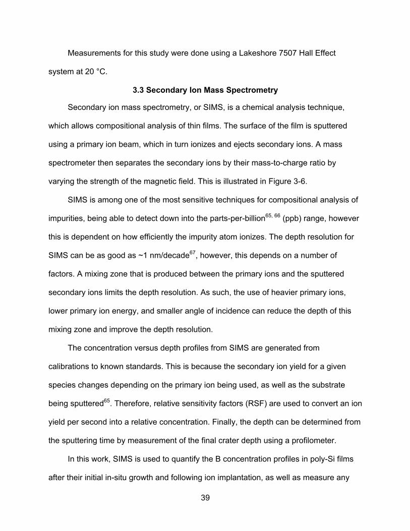
Secondary ion mass spectrometry, or SIMS, is a chemical analysis technique,
which allows compositional analysis of thin films. The surface of the film is sputtered
using a primary ion beam, which in turn ionizes and ejects secondary ions. A mass
spectrometer then separates the secondary ions by their mass-to-charge ratio by
varying the strength of the magnetic field. This is illustrated in Figure 3-6.
SIMS is among one of the most sensitive techniques for compositional analysis of
impurities, being able to detect down into the parts-per-billion65, 66 (ppb) range, however
this is dependent on how efficiently the impurity atom ionizes. The depth resolution for
SIMS can be as good as ~1 nm/decade67, however, this depends on a number of
factors. A mixing zone that is produced between the primary ions and the sputtered
secondary ions limits the depth resolution. As such, the use of heavier primary ions,
lower primary ion energy, and smaller angle of incidence can reduce the depth of this
mixing zone and improve the depth resolution.
The concentration versus depth profiles from SIMS are generated from
calibrations to known standards. This is because the secondary ion yield for a given
species changes depending on the primary ion being used, as well as the substrate
being sputtered65. Therefore, relative sensitivity factors (RSF) are used to convert an ion
yield per second into a relative concentration. Finally, the depth can be determined from
the sputtering time by measurement of the final crater depth using a profilometer.
In this work, SIMS is used to quantify the B concentration profiles in poly-Si films
after their initial in-situ growth and following ion implantation, as well as measure any
40
subsequent diffusion following flash-assisted rapid thermal annealing. A 3 kV Cs+
primary beam was used and concentration profiles were generated from the detection of
CsB- secondary ion clusters. This method eliminates the surface yield enhancement
seen when measuring B profiles using an O+ primary beam68.
3.4 3D Atom Probe Tomography
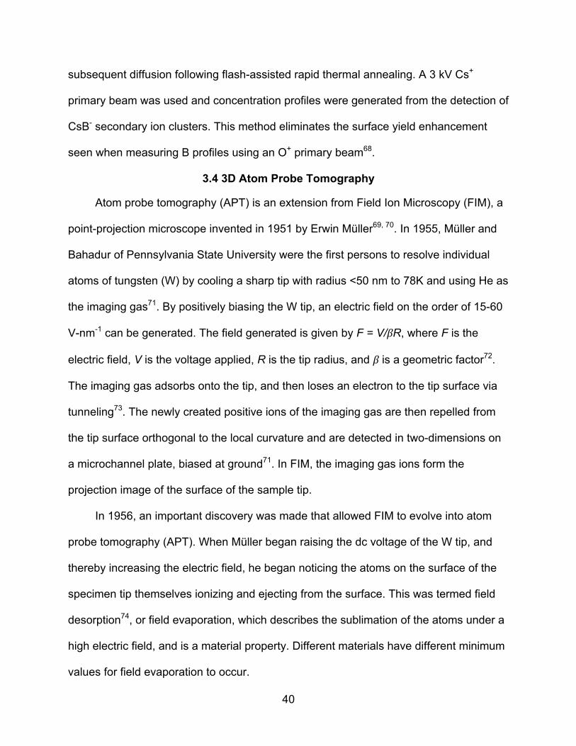
Atom probe tomography (APT) is an extension from Field Ion Microscopy (FIM), a
point-projection microscope invented in 1951 by Erwin Müller69, 70. In 1955, Müller and
Bahadur of Pennsylvania State University were the first persons to resolve individual
atoms of tungsten (W) by cooling a sharp tip with radius <50 nm to 78K and using He as
the imaging gas71. By positively biasing the W tip, an electric field on the order of 15-60
V-nm-1 can be generated. The field generated is given by F = V/βR, where F is the
electric field, V is the voltage applied, R is the tip radius, and β is a geometric factor72.
The imaging gas adsorbs onto the tip, and then loses an electron to the tip surface via
tunneling73. The newly created positive ions of the imaging gas are then repelled from
the tip surface orthogonal to the local curvature and are detected in two-dimensions on
a microchannel plate, biased at ground71. In FIM, the imaging gas ions form the
projection image of the surface of the sample tip.
In 1956, an important discovery was made that allowed FIM to evolve into atom
probe tomography (APT). When Müller began raising the dc voltage of the W tip, and
thereby increasing the electric field, he began noticing the atoms on the surface of the
specimen tip themselves ionizing and ejecting from the surface. This was termed field
desorption74, or field evaporation, which describes the sublimation of the atoms under a
high electric field, and is a material property. Different materials have different minimum
values for field evaporation to occur.

41
With this discovery, FIM underwent a radical evolutionary shift. No longer was an
imaging gas necessary to provide imaging of only the sample surface, but the ionization
of the samples themselves allowed a layer-by-layer analysis of the specimen being
analyzed.
The addition of a time-of-flight (TOF) detector75 dramatically shifted the scope of
the instrument from one of simply atomic imaging, to that of a tool for three-dimensional
imaging with materials analysis capabilities. TOF detectors allow calculation of each
individual ion’s (and their isotope’s) mass-to-charge ratio, allowing their unique
identification. From here, the addition of modern computing power and a two-
dimensional position sensitive detector has allowed the atom probe to evolve into a
three-dimensional tool for materials characterization76-79.
APT was traditionally limited to primarily refractory metals, with high conductivity
and the ability to withstand the high electric fields necessary for field evaporation.
Specimens were biased to just below the required electric field for evaporation, and
then the specimen voltage was pulsed at about .1-.2 of the standing voltage to induce
field evaporation one ion at a time and allow TOF calculations for each atom. The
advent of pulsed laser assisted atom probes has allowed the application of APT to
semiconducting materials such as Si72, 80-82 by using the laser as a thermal aid for
overcoming the field evaporation barrier. Laser pulses operate as fast as 500 khZ
allowing rapid data collection. In fact, recent advancements in laser technology has
allowed detailed analysis of even insulating materials such as oxides using
femtosecond laser pulses and ultraviolet wavelengths83-86. Figure 3-7 illustrates
operation of a pulsed-laser atom probe80.
42
3D APT allows a ~106 magnification for a 50 nm tip radius and 50 mm flight length.
The best achievable spatial resolution is on the order of 0.02 nm; in fact, (200) planes in
Si have been resolved using spatial distribution maps67, 71, 80, 81. This has allowed APT to
play an important role in materials research. Indeed, the relatively recent innovations
that allow analysis of electronic materials has led to many important findings, such as
dopant segregation to grain boundaries in polycrystalline Si46, 47, 87, gate oxide
segregation88, as well as direct imaging of dopant-defect interactions89, 90 and
clustering87, 91, 92. As a purely chemical analysis technique, it is used as an aid to
understanding the physical reasons for electronic properties in materials, but separate
electrical measurements must be made to validate any inferences from the atom probe
data.
Traditionally, thin wires for bulk metallic specimens were sharpened to a ~50 nm
radius using electropolishing71. However, electronic device structures are complex, and
often require site-specific sample preparation methods. The evolution of increasingly
diminutive transistor dimensions has lessened the disadvantages inherent in the
relatively limited analysis volume from APT. Indeed, site-specific analysis has been
achieved for many types of transistors; ranging from patterned structures to study lateral
As diffusion93, to high-electron mobility AlGaN/GaN HEMTs94, and even FinFET
structures95, 96.
This type of high-precision sample preparation is achieved using state-of-the-art
dual-beam focused-ion beam (FIB) systems with high-resolution scanning electron
microscope (SEM) capabilities and in-situ micromanipulation. The general procedure
has been well-documented in the literature97 and will be briefly discussed here.
43
In order to prevent implantation damage to the sample surface from the Ga+ beam
of the FIB, a thin ~50 nm layer of Ni is deposited on the sample surface. Figure 3-8
documents the lift-out procedure for MOSFET device fabricated on silicon-on-insulator
(SOI) using SEM imaging in the FIB. After locating the region of interest, ~100 nm Pt is
deposited in-situ using a gas-injection source to mark the area and further protect the
sample from ion beam damage. Two cuts are made at 30° to the sample normal to form
a wedge. An in-situ micromanipulator removes the wedge and transfers the sample to a
Si coupon with a 6×6 array of pillars. The wedge is sectioned off at a pillar and then
sharpened to a final tip radius ~50 nm using annular milling. The lift-out method can be
employed for both blanket wafers as well as devices requiring site-specificity.
3.5 Transmission Electron Microscopy
The transmission electron microscope (TEM) is used in this work to image the
microstructure of flash annealed poly-Si, which produces grain sizes on the order of
~20-100 nm. It allows extremely high magnification imaging by transmitting a beam of
electrons through an ultrathin sample and generating an image from the transmitted
beams. The principle behind such large magnifications comes from the fact that the de
Broglie wavelength98 of an electron is many orders of magnitude smaller than the
wavelength of light, and can be described by (3-10), where λ is the de Broglie
wavelength, h is Planck’s constant, and p is the relativistic momentum of the electron,
described by the electron’s mass m0, its charge e, the speed of light c, and the potential
U accelerating the electron to a certain velocity. A typical TEM may operate at an
accelerating voltage of 200 kV, which accelerates an electron to 70% of the speed of
light, producing a wavelength of only 2.5 pm.
44
λ =hp
=h
2m0eU1
1+eU2m0c
2
(3-10)
The source for electrons is typically a tungsten filament biased such that the work
function of the filament is exceeded and electrons are generated via thermionic
emission. Next, a series of electromagnetic condenser lenses focuses the electrons into
a coherent, monochromatic beam. The first lens determines the spot size while the
second lens determines the beam diameter on the sample. The beam passes through
the sample and undergoes a series of elastic and inelastic scattering processes. For
elastic scattering, Bragg’s law (3-11) states that electrons scattered by the same atomic
spacing, d, will scatter at the same angle, Θ,
λ = 2d sinΘ (3-11)
where λ is the wavelength of the incident beam. The diffracted beams create a
diffraction pattern of the material, which is a function of the sample orientation, crystal
structure, lattice spacing, and structure factor.
A final objective lens focuses the transmitted beams into an image, often projected
onto a phosphor screen or a CCD camera. The use of an objective aperture can allow
imaging from only a single diffracted beam, allowing increased contrast along specific
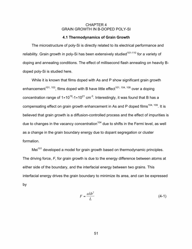
crystallographic orientations. Figure 3-9 depicts a ray diagram for the electron beam as
it moves through a series of lenses to produce the final image. Polycrystalline structures
such as the ones imaged in this study do not produce diffraction patterns with individual
spots, but instead due to the random orientation of the crystallites, diffraction rings are
observed. Transmission electron micrographs produced in this study were taken in the
bright field mode.
45
Because imaging in a TEM requires the transmission of electrons, specimens
must be made incredibly thin so as to be electron transparent. For Si, typically this
thickness is ~200 nm. For 120 nm poly-Si deposited on 12 nm SiO2, the preparation of
plan-view TEM (PTEM) samples involves a backside polish followed by a backside etch
until the desired thickness is achieved.
Poly-Si samples were cored into 3 mm discs and subsequently polished using SiC
paper at 250 and 600 grit to a thickness of ~100 μm. Then, samples were thinned down
to electron transparency using drip acid etching. The perimeter of each disc was
covered with wax so as to confine the etch to the center of the disc. The acid used was
a 3:1 volume ratio of 70% HNO3: 49% HF. The etch chemistry can be described
according to the equations99,
Si(s) + 4HNO3(l)⇔ 3SiO2 + 4NO(g) + 2H2O (3-12)
SiO2(s) + 6HF(l)⇔ H2SiF6(l) + 2H2O (3-13)
Essentially, the nitric acid serves to oxidize the Si surface and then the hydrofluoric acid
etches the resulting SiO2 away.
Alternatively, cross-sectional orientation samples (XTEM) were prepared using a
dual-beam focused-ion beam (FIB). The sample surface is first protected with ~60 Å
graphitic C, and then marked using in-situ gas injection Pt for further protection from the
Ga+ ion beam operating at 30 kV. XTEM samples ~100 nm in thickness were produced
by continual focused ion beam milling, and subsequently removed and placed onto C
grids using micromanipulators100.

46
The TEM images in this study were taken with a JEOL 200CX microscope
operating at 200 kV using bright field imaging mode.
47
Figure 3-1. Schematic representation of four-point probe measurement.
Figure 3-2. Sample geometry for deriving sheet resistance from resistivity.
Figure 3-3. Illustration demonstrating the Hall voltage VH arising due to the Lorenz
force from application of a magnetic field, B.
48
Figure 3-4. Illustration of the van der Pauw Hall Effect geometry.
Figure 3-5. Determining characteristic resistance RA and RB using van der Pauw
technique.

49
Figure 3-6. Illustration of ion analysis from secondary ion mass spectrometry.
Figure 3-7. Diagram demonstrating pulsed-laser assisted atom probe operation.
(Source: T. F. Kelly, International Conference on Frontiers of Characterization and Metrology for Nanoelectronics, 2007)
50
Figure 3-8. Sample preparation for APT using the lift-out method for a MOSFET on
SOI. A) In-situ micromanipulator removes wedge formed from angular cuts in front and behind using the ion beam. B) transfer of a portion of the wedge to a pillar for sharpening via annular milling. C) final tip sharpened showing placement of the device layer in the center of the tip.
Figure 3-9. Ray diagram demonstrating the path of the electron beam traveling from
source to final image in a TEM.
51
CHAPTER 4 GRAIN GROWTH IN B-DOPED POLY-SI
4.1 Thermodynamics of Grain Growth
The microstructure of poly-Si is directly related to its electrical performance and
reliability. Grain growth in poly-Si has been extensively studied101-110 for a variety of
doping and annealing conditions. The effect of millisecond flash annealing on heavily B-
doped poly-Si is studied here.
While it is known that films doped with As and P show significant grain growth
enhancement101, 103, films doped with B have little effect101, 104, 108 over a doping
concentration range of 1×10¹⁹-1×1021 cm-3. Interestingly, it was found that B has a
compensating effect on grain growth enhancement in As and P doped films104, 109. It is
believed that grain growth is a diffusion-controlled process and the effect of impurities is
due to changes in the vacancy concentration104 due to shifts in the Fermi level, as well
as a change in the grain boundary energy due to dopant segregation or cluster
formation.
Mei101 developed a model for grain growth based on thermodynamic principles.
The driving force, F, for grain growth is due to the energy difference between atoms at
either side of the boundary, and the interfacial energy between two grains. This
interfacial energy drives the grain boundary to minimize its area, and can be expressed
by
F =aλb2
L (4-1)
52
where λ is the grain boundary energy, b is the lattice constant, L is the grain diameter,
and a is a geometric factor. If growth is diffusion controlled, then the grain boundary
mobility should be directly proportional to the Si self-diffusivity.
µ =Dg
kT (4-2)
Eq. (4-3) describes the grain boundary mobility, μ, where Dg is the self-diffusivity of
Si. The product of the mobility and driving force equals the boundary migration rate,
which describes the growth rate
dLdt
= µF =aλb2Dg
LkT (4-3)
By integration, the grain size L can be determined in terms of the initial grain size
L0, where
L = L02 +2ab2
kTλDSit
⎡
⎣ ⎢
⎤
⎦ ⎥
1/ 2
(4-4)
assuming the grain-boundary energy and Si self-diffusivity does not vary with time. It
has been shown that for primary grain growth, such as the case for B doped poly-Si,
grain sizes are limited to the thickness of the film101, 111.
This thickness effect is due to the variation in grain boundary energy when the
grains come in contact with the oxide layer. As grains grow larger, this effect becomes
more pronounced since more grain surface mobility is slowed at this interface. This
effect has been modeled using
λ =λ0
1+ h 2Al
(4-5)

53
where A is the grain boundary area per volume (3/L), l is the thickness of the film and h
is a fitting constant that was experimentally determined to be 6.
4.2 Experimental Conditions
120-nm poly-Si films deposited on 12 nm SiO2 were doped in-situ to a total dose of
2.5×1015 cm-2. Half of the samples were then preamorphized using Ge+ implantation at
40 keV to a dose of 5×1014 cm-2, creating a 60 nm continuous amorphous region. The
samples receiving the Ge+ preamorphization were then further ion implanted with B+ to
bring the total dose of the film to 4.9×1015 cm-2. Cross-sectional TEM micrographs of the
as-deposited and as-implanted poly-Si films are shown in Figure 3-1. Their
corresponding initial doping profiles as measured by SIMS are shown in Figure 3-2.
The films were then annealed using a flash-assist rapid thermal annealing to peak
temperatures of 1150 °C, 1250 °C, and 1350 °C. The intermediate pre-flash
temperature was 850 °C. An example of a typical temperature profile from the Mattson
Millios™ tool used is shown in Figure 3-3. The pulse width is approximately 1.0 ms. For
reference, samples were also annealed using conventional rapid thermal annealing at
988 °C for 5 s.
Following annealing, samples were prepared for plan-view transmission electron
microscopy (PTEM) in order to measure grain size distributions. This was done by
coring 3 mm discs from each wafer and backside mechanical polishing until ~100 μm
thickness. Samples were then further thinned from the backside using an acid etchant
of 75% HNO3 (70% conc) to 25% HF (49% conc) until electron transparent. Films were
imaged using a JEOL 200CX TEM operating at 200 keV.
54
4.3 Results and Discussion
PTEM revealed as-deposited films as having a very fine microstructure with an
average grain diameter of 19 nm. Upon flash annealing, grains became more refined
and coarsened to an average diameter of 52 nm in the in-situ doped case and 59 nm in
samples with the additional Ge+ and B+ implant at 1350°C. The amorphous region
showed full regrowth at the pre-flash temperature, so there was no regrowth of any
amorphous phase during the flash part of the anneal. Secondary grain growth was not
observed, and was not expected based on previous literature105, 106.
Grain growth enhancement has been reported to be correlated to hole
concentration104, with slightly greater enhancement at temperatures above 1100 °C112.
In Hall effect measurements, it was shown that implanted samples that are flash
annealed using a 950 °C pre-flash temperature have an approximately 25% lower hole
concentration. Despite a slightly higher thermal budget, grain size measurements for
this anneal condition fell in between that of the in-situ doped sample and the implanted
sample using an 850 °C pre-flash temperature. This confirms the model proposed by
Kim104, which predicts enhancement as a function of hole concentration, but even their
model shows the enhancement to only be up to 25% at 1000 °C for the narrow range of
hole concentrations studied here. The significant overlap in error bars between the in-
situ doped and implanted samples implies that there is not a significant difference in
grain growth between the two doping concentrations, and this has been confirmed
experimentally101 for B concentrations between 1×10¹⁹-1×1021 cm-3 at annealing
temperatures between 900-1200 °C. However, Hall measurements shown later reveal
that these minor differences in grain size reveal themselves in mobility values.
55
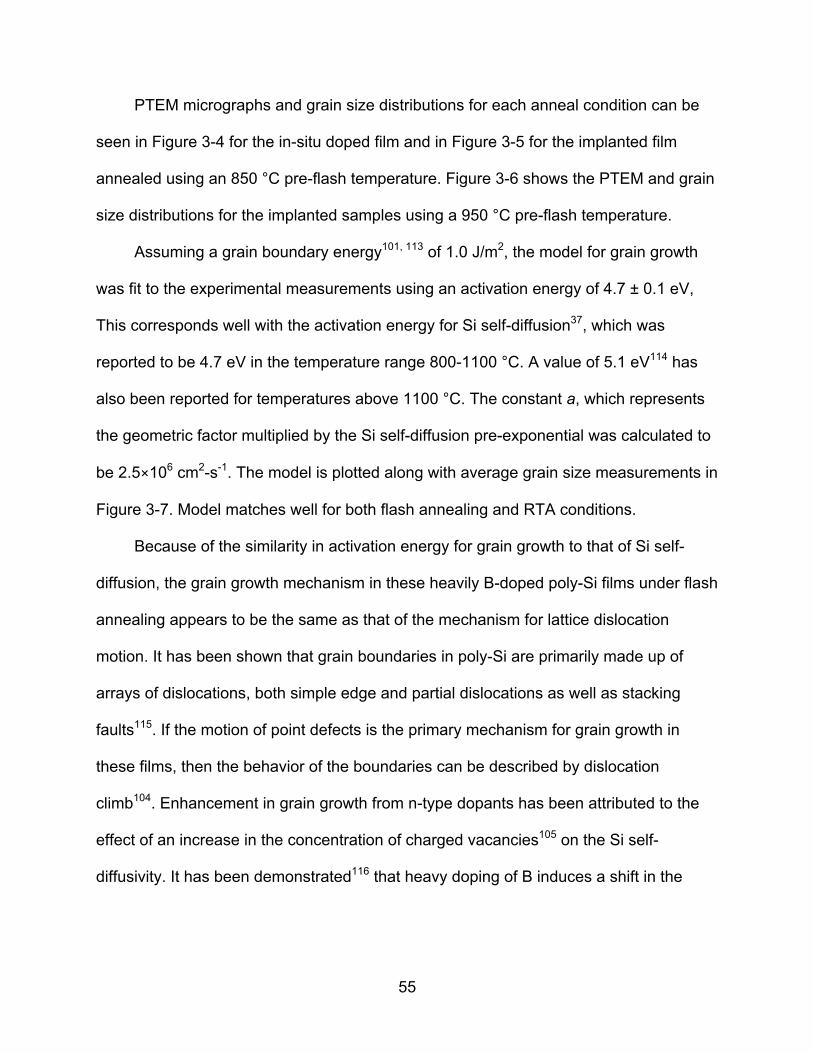
PTEM micrographs and grain size distributions for each anneal condition can be
seen in Figure 3-4 for the in-situ doped film and in Figure 3-5 for the implanted film
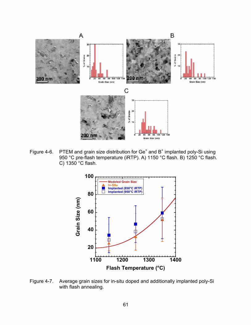
annealed using an 850 °C pre-flash temperature. Figure 3-6 shows the PTEM and grain
size distributions for the implanted samples using a 950 °C pre-flash temperature.
Assuming a grain boundary energy101, 113 of 1.0 J/m2, the model for grain growth
was fit to the experimental measurements using an activation energy of 4.7 ± 0.1 eV,
This corresponds well with the activation energy for Si self-diffusion37, which was
reported to be 4.7 eV in the temperature range 800-1100 °C. A value of 5.1 eV114 has
also been reported for temperatures above 1100 °C. The constant a, which represents
the geometric factor multiplied by the Si self-diffusion pre-exponential was calculated to
be 2.5×106 cm2-s-1. The model is plotted along with average grain size measurements in
Figure 3-7. Model matches well for both flash annealing and RTA conditions.
Because of the similarity in activation energy for grain growth to that of Si self-
diffusion, the grain growth mechanism in these heavily B-doped poly-Si films under flash
annealing appears to be the same as that of the mechanism for lattice dislocation
motion. It has been shown that grain boundaries in poly-Si are primarily made up of
arrays of dislocations, both simple edge and partial dislocations as well as stacking
faults115. If the motion of point defects is the primary mechanism for grain growth in
these films, then the behavior of the boundaries can be described by dislocation
climb104. Enhancement in grain growth from n-type dopants has been attributed to the
effect of an increase in the concentration of charged vacancies105 on the Si self-
diffusivity. It has been demonstrated116 that heavy doping of B induces a shift in the

56
Fermi level, which reduces the number of charged vacancies. This likely explains why B
does not enhance grain growth in the way P and As doping do.

57
Figure 4-1. Cross-sectional transmission electron micrograph of poly-Si film. A) as-deposited poly-Si film. B) after Ge+ preamorphization implant and B+ implant.
Figure 4-2. SIMS profiles for initial B concentrations for as-deposited and with additional Ge+ and B+ implant

58
Figure 4-3. Temperature profile for a 1350 °C flash anneal with a pre-flash temperature of 950 °C.
59
Figure 4-4. PTEM and grain size distribution for in-situ B doped poly-Si. A) as-deposited. B) 1150 °C flash. C) 1250 °C flash. D) 1350 °C flash. E) 988 °C RTA.

60
Figure 4-5. PTEM and grain size distribution for Ge+ and B+ implanted poly-Si. A) 850 °C iRTP (no flash). B) 1150 °C flash. C) 1250 °C flash. D) 1350 °C flash. E) 988 °C RTA.
61
Figure 4-6. PTEM and grain size distribution for Ge+ and B+ implanted poly-Si using
950 °C pre-flash temperature (iRTP). A) 1150 °C flash. B) 1250 °C flash. C) 1350 °C flash.
20
40
60
80
100
1100 1200 1300 1400
Modeled Grain Size
Implanted (850°C iRTP)In-SItu
Implanted (950°C iRTP)
Gra
in S
ize
(nm
)
Flash Temperature (°C)
Figure 4-7. Average grain sizes for in-situ doped and additionally implanted poly-Si with flash annealing.
62
CHAPTER 5 MOBILITY, ACTIVATION, AND DEACTIVATION OF B-DOPED POLYSILICON WITH
FLASH ANNEALING
5.1 Poly-Si in HBT Technology
As microelectronics processing begins to adapt advanced annealing methods
such as millisecond flash annealing8, 10, it is important to understand the effect of these
processing conditions beyond that of crystalline Si. Poly-Si has many applications in
CMOS device fabrication6 and continues to play a crucial role in devices such as
heterojunction bipolar transistors (HBT)5, 7.
When compared to c-Si, the most obvious separation is the presence of grain
boundaries. Grain boundaries primarily act as scattering sites and potential barriers59
leading to reduced carrier mobility in polysilicon49. However, at sufficiently high doping
levels, the resistivity of polysilicon can approach that of single-crystalline silicon49 due to
the reduced carrier mobility in both environments from high concentrations of active,
ionized impurities, which also act as scattering sites. Additionally, the existence of grain
boundaries is often a lower energy state for dopants to segregate to and deactivate45,
113. This has been reported for As45, 46 and P45, but is less often seen for B except at
very high concentrations3, 47.
One of the advantages of the presence of grain boundaries is their ability to act as
recombination centers for point defects43. It has been shown that grain boundaries act
as an effective sink for vacancies, and this may also be true for interstitials. While
millisecond annealing techniques such as flash and laser annealing have allowed very
high activation with minimal diffusion, the observance of post-annealing dopant
deactivation is also of concern. For As, the deactivation is attributed to formation of As
clusters with vacancies117 in c-Si. In poly-Si, As segregation to the grain boundaries45, 53
63
was seen with cyclical anneal cycles. In the case of B, deactivation has been found to
occur due to the presence of {311} defects present in the end-of-range following
preamorphizing implants that have not been dissolved with the minimal thermal budget
of millisecond annealing118-120. This mechanism for deactivation should be minimized in
a polycrystalline structure if the grain boundaries are significant sinks for excess
interstitials.
Oftentimes in device fabrication processing, use of single-crystalline silicon for
some structures is simply unfeasible due to the lack of a crystalline surface to act as a
seed for epitaxy5, 6. One such example is in the case of high-performance SiGe:C HBTs,
where poly-Si forms the elevated extrinsic base in the base layer of the structure and is
deposited over oxide5. A schematic is illustrated in Figure 5-1. Improving the transit
frequency, fT, and the maximum oscillation frequency, fMAX, has proven to be
challenging due to compensating effects for a given thermal budget. A low thermal
budget aids in delivering the highest transit frequencies due to reduced diffusion in the
base, thereby allowing a thin base width7. However, due to the increased base
resistance under these thermal processing conditions, fmax is reduced.
With this in mind, the application of flash annealing to B-doped poly-Si presents
itself very favorably7, 8. High temperature annealing (up to 1350°C) allows greater B
solubility9, and therefore lower resistance, while short annealing timescales significantly
limits diffusion8. The typical pulse width10 for flash annealing is on the order of 1 ms.
While the scope of this paper focuses on the electrical properties of poly-Si in its
application as the elevated extrinsic base in bipolar CMOS technology5, the results
64
presented form a fundamental basis for understanding the effect of millisecond
annealing on sheet resistance, activation, and mobility of heavily B-doped poly-Si films.
5.2 Experimental Methods
120 nm polysilicon films were deposited by low-pressure chemical vapor
deposition on 12 nm of oxide over bulk Si wafers and in-situ doped with B during film
growth. The total dose of the in-situ doped film is 2.5 x 1015 cm-2 and represents an
environment below solid solubility at higher flash temperatures. Some films are
additionally doped via ion implantation using first a Ge+ pre-amorphization implant at 40
keV to a dose of 5 x 1013 cm-2. This forms a continuous amorphous layer of 60 nm. After
pre-amorphization, an additional 10 keV B+ implant is added to bring the total dose to
4.9 x 1015 cm-2, as measured by SIMS. In this case, for all annealing temperatures, the
peak concentration of B is above solubility. As-deposited and as-implanted profiles for
both samples are shown in Figure 5-2.
Films were then flash annealed using an impulse rapid thermal process to a pre-
flash temperature (iRTP) of 850 °C and flashed to temperatures of 1150°C, 1250°C, and
1350°C. For comparison, a 950 °C iRTP was also investigated. Finally, the effect of an
RTA anneal at 988 °C for 5 s prior to annealing with the flash system was examined.
In c-Si, the use of an RTA pre-anneal has been shown to improve sheet resistance
by removing EOR defects from implantation120. Also, because poly-Si gates for CMOS
are typically doped at the source-drain implantation step, the significantly reduced
diffusion seen with flash annealing leads to “poly depletion”30 in the gate, which can
become the dominant effect in gate capacitance. Because diffusion in poly-Si is
significantly greater than in crystalline Si due to the presence of grain boundaries29, a
short, lower temperature RTA allows sufficient dopant to reach the poly/gate oxide

65
interface. It is hoped that activation can be further improved using flash annealing in
addition to conventional RTA.
Post-flash annealing was carried out using 30 min furnace anneals under N2
ambient between 400-800°C to study thermal stability of the dopant. Hall measurements
were only done on 850 °C iRTP samples annealed at 650 °C and above because
noticeable deactivation did not begin to occur until that temperature.
Electrical measurements were done with a Lakeshore 7507 Hall measurement
system using the Van Der Pauw method61. Doping levels were sufficiently high such
that good ohmic conduction (r ≥ .99) was achieved using indium-gallium contacts. Due
to the high concentration of dopant in the material, sheet number measurements were
calculated using a Hall Scattering Factor of 0.763. Prior work121-123 for Hall
measurements in polycrystalline structures has demonstrated that for sufficient doping,
the Hall constant should be accurate in measuring the carrier concentration within the
grains. This is because when doping far exceeds the carrier trap density, as is the case
in the films studied here, the potential barrier at the grain boundary is very small (~5
meV)57.
5.3 Electrical Activation and Mobility
Sheet resistance measurements are displayed in Figure 5-3 for both the as-
deposited in-situ doped samples as well as the implanted samples using an 850°C and
950°C pre-flash temperature. Values for samples that were pre-annealed by RTA are
also plotted. By effectively doubling the dose of the dopant, sheet resistance values fall
roughly 40-50% for all flash temperatures. No difference was observed in sheet
resistance by using a 950 °C pre-flash temperature. Sheet resistance improves linearly
with RTA pre-anneal and exponentially with only flash anneal. This is due to both
66
activation and mobility improvements with flash annealing, whereas an RTA pre-anneal
grows the grains appreciably prior to flash. This is verified in Figure 5-4 where mobility
values are clearly seen to be set by the RTA pre-anneal. Grain size measurements
reported previously reveal that the 988 °C 5s RTA anneal is roughly equivalent to a
1250 °C flash anneal in terms of grain growth. Further mobility improvements at 1350
°C flash temperatures are likely compensated by the increase in carrier concentration
leading to a reduction in expected mobility due to ionized impurity scattering.
Active sheet number values, shown in Figure 5-5, increase linearly with flash
temperature. Despite the increased activation with temperature, mobility values
continue to rise. This is due to grain growth, which was verified with plan-view
transmission electron microscopy (PTEM). While both the in-situ doped and implanted
samples show almost identical microstructures for a given anneal condition, there is a
slight improvement in mobility for the implanted sample with roughly twice the dose. In
c-Si, such a high activation would lead to a lower mobility due to ionized impurity
scattering. Seto’s57 measurements for hole mobility shows an increasing trend from
5×10¹⁸ - 5×1019 cm-3 doping concentrations. The active concentrations shown here are
above 1×1020 cm-3, up to as high as 4×1020 cm-3. This represents a concentration
regime outside of his work. Kamins58 reported a peak mobility in poly-Si at a hole
concentration of 2.5×1018 cm-3, and reduced mobility for concentrations above that
regime. However, a major difference in their work is the grain size in the films; Seto
reported an average grain size of 20 nm while Kamins reported grain sizes as large as
500 nm in a 5 µm film. The finer grain microstructure in Seto’s film more accurately
resembles the microstructure of the films in this study. The prevalence of so many
67
boundaries may act as a significant source for resistivity, and so it should follow that a
higher concentration of active B, which effectively lowers the grain boundary potential
barrier15, 57, 59 can also improve the hole mobility. At larger grain sizes, it is likely that
other factors that increase resistance such as impurity scattering play a more significant
role.
Unlike the n-type dopants As and P, B has been shown to enhance grain growth
only slightly, and this enhancement does not vary noticeably with B concentration101, 104.
Also, B doped poly-Si films do not undergo secondary grain growth, where grain sizes
grow beyond the film thickness105, 106 driven by the surface energies of certain grain
orientations. This type of grain growth has been previously seen to occur significantly
with P and less so with As doped poly-Si104-109. Due to millisecond annealing times with
flash annealing, grain sizes in this study do not grow appreciably, beginning with an
average grain size of 19 nm and reaching a grain size of 59 nm at 1350°C. There was
not a significant difference in microstructure for samples that received the Ge
preamorphization implant, additional B implant, or 950 °C iRTP anneal.
For implanted samples, there is a roughly 25% lower sheet number measured for
samples flash annealed from a 950 °C iRTP temperature instead of 850 °C iRTP.
Further reductions in activation were seen with RTA pre-annealed samples. These
values are plotted in Figure 5-5. This effect was not significant in the in-situ doped
samples, suggesting that this is an effect from the additional implants. Possible causes
for this reduced activation can be attributed to defect induced cluster formation or
segregation to grain boundaries.
68
Preamorphization by ion implantation and solid phase epitaxial regrowth (SPER)
has been used extensively in c-Si to improve activation of dopant by direct incorporation
into substitutional sites on the lattice during regrowth. The solubility levels achieved
using this process22 is of the order of a few 1020 cm-3 and almost independent of
temperature23, however, there have been reports that suppression of regrowth by using
a low pre-flash temperature allows higher activation when regrowth occurs during the
high temperature “flash” portion of the temperature profile124, 125. This is not the case
seen here since the amorphous layer shows full regrowth with only the 850 °C iRTP
anneal. Because SPER allows activation above equilibrium values, thermal processing
after regrowth can lead to a deactivation simply as a return to equilibrium.
Figure 5-6 compares the sheet number values for flash annealed samples to RTA
samples. 850 °C and 950 °C data points represent the spike anneal from the iRTP while
988 °C represents the 5s conventional RTA. They are plotted together as RTA since
their anneal times are significantly longer than the flash. Also plotted are the calculated
theoretical activation curves based on solubility data for c-Si9. It is evident that because
of SPER, activation prior to flash is above solid solubility for the implanted case. This
difference in initial solubility benefit from the lower iRTP temperature accounts for
greater activation when flash occurs.
The larger differences at higher flash temperatures suggests a separate pre-flash
deactivation process, most likely attributable to cluster formation. Creation of the
amorphous layer from ion-implantation has been known to deactivate B due to the
interstitials generated at the end-of-range leading to boron-interstitial cluster
formation126. However, the high temperature activation does not follow either path of

69
typical boron-interstitial-cluster (BIC) dissolution41. Similar behavior to that reported here
was seen with flash-annealed samples in crystalline Si127, and is suggested to be
formation of a less stable cluster, which dissolves at high temperatures.
Figure 5-7 shows work from Castillo-Camillo127 involving flash annealing of
crystalline Si with similar conditions studied here in poly-Si. B was implanted at 1 kV to
a dose of 1×1015 cm-2. A Ge preamorphizing implant was also done at 30 kV to a dose
of 1×1015 cm-2 and subsequently flash annealed to temperatures between 1000 °C –
1300 °C using a 700 °C iRTP. Similar to the results in poly-Si, activation begins above
solid solubility at lower temperatures due to solid phase regrowth. However, at the
highest flash temperature, activation is below theoretical levels and this was attributed
to cluster formation. This is in contrast to the results from this study in poly-Si, which
suggests that cluster formation may be reduced in a polycrystalline structure, where
excess interstitials may be absorbed by the grain boundaries.
5.4 Electrical Deactivation and Mobility
Post-flash deactivation measurements were made for 850 °C iRTP samples only.
Sheet resistance measurements for samples flashed to 1350 °C are shown in Figure 5-
8. Significant rise in sheet resistance was seen only above 650 °C for constant 30 min
anneals. Grain size measurements confirm that there is no detectable increase in
average grain size for samples annealed at 800 °C for 30 min, allowing for activation
and mobility measurements at a constant grain size.
Activation values are plotted in Figure 5-9 for all flash temperatures. Values for
activation converge at 800 °C, but implanted samples retain roughly 50 percent more
activated dopant. This is unexpected and will require further study. The number of
deactivated carriers can be calculated by subtracting the final activation value from the
70
initial activation value. For all flash temperatures below 1350 °C, the calculated
activation energy for deactivation is roughly 1.0±0.2 eV. For 1350 °C flash
temperatures, both the in-situ doped and implanted samples retain more activation at
650 °C, but follows the same trend at 700 °C and above. This is likely to be related to
grain boundary segregation, since the lower flash temperatures have smaller grains.
Segregation values tend to be higher at lower temperatures45 due to more available
grain boundary surface area.
Mobility measurements following deactivation anneals are shown in Figure 5-10.
Because there was no measurable grain growth from these anneals, the mobility gains
are directly related to the reduction in active ionized impurities. The lowest average hole
concentration measured is 5×1019 cm-3, which corresponds to an estimated grain
boundary potential barrier of only 5 meV according to Seto’s model57. Therefore,
mobility gains from deactivation can be solely attributed to less ionized impurity
scattering.
Modeling for mobility in poly-Si has been done by using Mathiessen’s formula128 to
combine scattering terms from majority carrier scattering, µi,maj, grain boundary potential
boundary scattering, µEb, and a third extracted term describing the influence of grain
size, denoted as µGB. The overall mobility can be expressed as,
µ =1
µi,maj+1
µEb
+1
µGB
⎛
⎝ ⎜ ⎜
⎞
⎠ ⎟ ⎟
−1
(5-1)
Majority carrier scattering has been well studied129, and can be described by
µi,maj = µ0 +µmax − µ0
1+ N /Cref ,1( )α1−
µ1
1+ Cref ,2 /N( )α2
(5-2)
71
where N is the concentration of holes, and the other parameters are given in Table 5-1.
The influence of minority carrier scattering is ignored here due to the heavy doping
concentration of the material.
Next, scattering by the grain boundary due to the formation of potential barriers
was modeled by Seto57 and was discussed in Chapter 2. At the doping concentrations
studied here, the magnitude of grain boundary potential barrier formed is almost
inconsequential, however, it is included to better represent the poly-Si environment at
lower concentrations. The mobility term, µEb, can be described by
µEb = Lq 12πm * kT⎛
⎝ ⎜
⎞
⎠ ⎟ 1/ 2
exp −EB
kT⎛
⎝ ⎜
⎞
⎠ ⎟ (5-3)
where L is the grain size, q is the elementary charge, and EB represents the energy
barrier required for a carrier to pass over the grain boundary, given by
EB =qQt
2
8εN (5-4)
where N is the average hole concentration, Qt represents the trap state density
(3.34×1012 cm-2)57, and ε is the dielectric permittivity of poly-Si.
Finally, given the mobility terms for majority carrier scattering and potential barrier
scattering, a fitting term representing the influence of the grain size on the overall
mobility in poly-Si was extracted. µGB is of the form Aexp(-β), where
A =1.8 ×10¹²L2 +1.7 ×10⁶L + 25 (5-5)
and
β =1.78 ×10²⁰N exp(−3.34 ×10⁵L) (5-6)
72
Applying Mathiessen’s formula, Figure 5.10 plots the mobility behavior with
deactivation for each initial flash condition for the in-situ doped and implanted samples,
while the models are generated with the grain sizes measured from PTEM. Sheet
numbers have been converted to an average concentration within the film. The model
agrees well with the experimental data. Mobility values measured here for poly-Si are
roughly half that of c-Si129 for a given active carrier concentration, suggesting that both
impurity concentration and microstructure play a role in determining mobility in these
films.
5.5 Summary
Hall measurements for flash annealed poly-Si samples have provided significant
insight into the activation and mobility behavior for heavily B-doped films. Activation
improvements with lower iRTP temperatures have been attributed to the above
equilibrium activation achievable using the SPER process. Reduced activation from
increasing pre-flash thermal budget was therefore shown to be attributed to a reduction
in pre-flash activation following regrowth of the amorphous layer.
Mobility measurements upon activation and deactivation verify that mobility is a
function of both active concentrations of dopant as well as microstructure. The linear
behavior in mobility improvement with flash annealing suggests the compensating effect
between increasing grain size (improved mobility) and increasing activation (reduced
mobility). By holding microstructure constant, deactivation studies show increases in
mobility values due to less ionized impurity scattering. Mobility values have been
accurately modeled over the deactivation temperature range of 650 °C to 800 °C. It has
been shown that Seto’s model, which assumes grain boundary scattering to be the
dominant reason for resistivity, cannot apply completely in such highly doped material.

73
The difference in mobility between poly-Si and c-Si values129 suggest that both ionized
impurity scattering and grain boundary scattering contribute to the overall mobility in
poly-Si films.

74
Parameter Holes (p-type Si)
µmax 470.5
µ0 44.9
µ1 29
α1 0.719
α2 2.0
Cref,1 2.23×10¹⁷
Cref,2 6.10×10²⁰
Table 5-1. Majority carrier simulation parameters.
Figure 5-1. Schematic showing elevated extrinsic base for a heterojunction bipolar transistor. Epitaxial growth is allowed over the crystalline heavily-doped collector but not over STI.

75
1018
1019
1020
1021
0 20 40 60 80 100 120 140
As-Depositedw B Implant
Con
cent
ratio
n (a
tom
s/cm
3 )
Depth (nm)
Figure 5-2. SIMS profile comparison for initial B concentrations for as-deposited and with additional Ge+ and B+ implant.
0
100
200
300
400
500
1100 1200 1300 1400
In-Situ 850°C iRTPImplanted 850°C iRTPIn-Situ 950°C iRTPImplanted 950°C iRTPRTA + 850°C iRTP In-SituRTA + 850°C iRTP ImplantedRTA + 950°C iRTP In-SItuRTA + 950°C iRTP Implanted
Shee
t Res
ista
nce
(ohm
s/sq
)
Flash Temperature °C
Figure 5-3. Sheet resistance comparison between as-deposited in-situ doped and additionally B implanted poly-Si films at various flash anneal conditions.
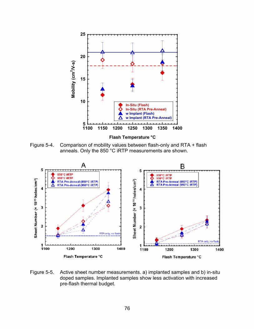
76
5
10
15
20
25
1100 1150 1200 1250 1300 1350 1400
In-Situ (Flash)In-Situ (RTA Pre-Anneal)w Implant (Flash)w Implant (RTA Pre-Anneal)
Mob
ility
(cm
2 /V-s
)
Flash Temperature °C
Figure 5-4. Comparison of mobility values between flash-only and RTA + flash anneals. Only the 850 °C iRTP measurements are shown.
Figure 5-5. Active sheet number measurements. a) implanted samples and b) in-situ doped samples. Implanted samples show less activation with increased pre-flash thermal budget.
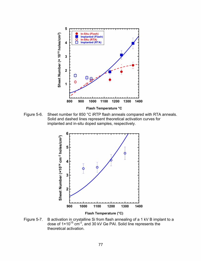
77
Figure 5-6. Sheet number for 850 °C iRTP flash anneals compared with RTA anneals.
Solid and dashed lines represent theoretical activation curves for implanted and in-situ doped samples, respectively.
Figure 5-7. B activation in crystalline Si from flash annealing of a 1 kV B implant to a
dose of 1×1015 cm-2, and 30 kV Ge PAI. Solid line represents the theoretical activation.
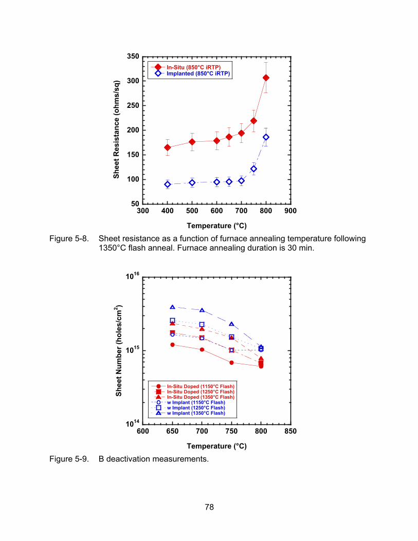
78
300 400 500 600 700 800 900
In-Situ (850°C iRTP)Implanted (850°C iRTP)
50
100
150
200
250
300
350
Temperature (°C)
Shee
t Res
ista
nce
(ohm
s/sq
)
Figure 5-8. Sheet resistance as a function of furnace annealing temperature following
1350°C flash anneal. Furnace annealing duration is 30 min.
1014
1015
1016
600 650 700 750 800 850
In-Situ Doped (1150°C Flash)In-Situ Doped (1250°C Flash)In-Situ Doped (1350°C Flash)w Implant (1150°C Flash)w Implant (1250°C Flash)w Implant (1350°C Flash)
Shee
t Num
ber (
hole
s/cm
2 )
Temperature (°C)
Figure 5-9. B deactivation measurements.
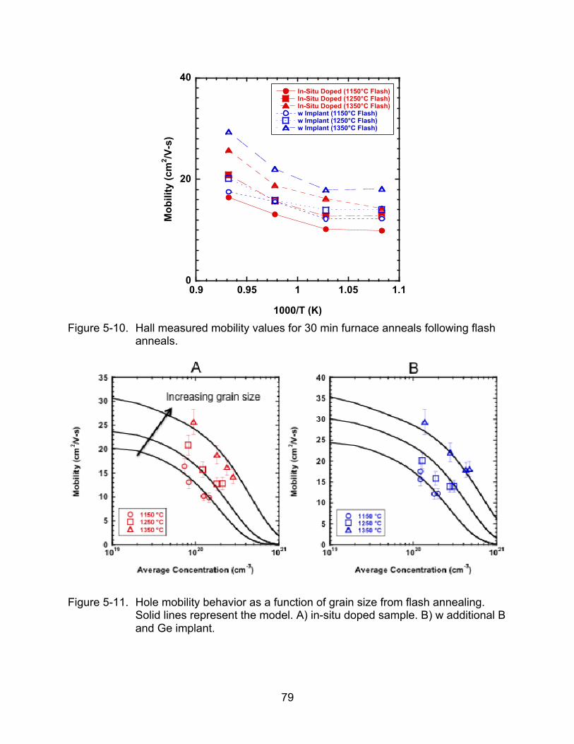
79
0
20
40
0.9 0.95 1 1.05 1.1
In-Situ Doped (1150°C Flash)In-Situ Doped (1250°C Flash)In-Situ Doped (1350°C Flash)w Implant (1150°C Flash)w Implant (1250°C Flash)w Implant (1350°C Flash)
Mob
ility
(cm
2 /V-s
)
1000/T (K)
Figure 5-10. Hall measured mobility values for 30 min furnace anneals following flash anneals.
Figure 5-11. Hole mobility behavior as a function of grain size from flash annealing. Solid lines represent the model. A) in-situ doped sample. B) w additional B and Ge implant.

80
CHAPTER 6 B SEGREGATION TO GRAIN BOUNDARIES AND DIFFUSION IN
POLYCRYSTALLINE SI WITH FLASH ANNEALING
6.1 Importance of Dopant Segregation
Polycrystalline Si, or poly-Si, has many applications in the field of microelectronic
devices, from conventional field-effect transistors6, to heterojunction bipolar transistors5,
and photovoltaics130. Due to the ever-shrinking feature sizes in transistors, innovations
in annealing beyond conventional rapid thermal processing are necessary to limit
diffusion and increase activation of dopants7. In particular, flash annealing allows low
thermal budgets with high temperatures and very short time scales on the order of 1
ms8. The combination of high B concentration with low thermal budgets presents an
ideal environment for B segregation to the grain boundaries in poly-Si. The degree of
segregation can have a profound effect on B diffusion due to the significantly enhanced
diffusivity of impurities within grain boundaries. Also, segregated dopants are electrically
inactive and reduce the conductivity of the material. Therefore, it is important to
understand the effect of millisecond annealing on B doped poly-Si films.
Three-dimensional atom probe tomography (APT) allows direct analysis of dopant
segregation to grain boundaries and other crystalline defects89, 90, 131. In fact, the
technique has already been employed to demonstrate segregation of As and P to grain
boundaries in a polysilicon gate electrode46. However, there have been conflicting
reports as to the segregation of B to grain boundaries. Inoue et al. has shown that it
does not segregate46 while atom probe measurements from Thompson et al. show
significant segregation47 at grain boundary triple points. Even prior to 3D APT, B
segregation to grain boundaries was debatable. Activation and deactivation with cyclical
annealing was seen for As doped poly-Si, but not for B for concentrations below solid
81
solubility45. On the other hand, it has also been reported that at very high
concentrations, (>2 at%) B formed precipitates at the grain boundaries of poly-Si3. In
this work, a weak but detectable segregation of B to the grain boundaries is reported
using 3D APT. Grain growth was found to significantly reduce the amount of segregated
B due to the reduction in grain boundary surface area. Values obtained from the
experimental data were applied to a poly-Si diffusion model51, 52, which accurately
predicts diffusion of B in flash annealed poly-Si. Hall measurements suggest that the
segregated B is electrically inactive.
6.2 Experimental Methods
120 nm poly-Si films were deposited by low-pressure chemical vapor deposition
on bulk Si wafers with ~12 nm of SiO2. B doping was done in-situ to a total dose of 2.5 ×
1015 cm-2, which amounts to a peak concentration below the solid solubility level9 of 3.0
× 1020 cm-3 for anneal temperatures above 1250 °C. Additionally, some samples were
further doped by ion implantation, beginning with a preamorphizing implant using Ge+ at
40 keV to a dose of 5.0 × 1014 cm-2, followed by an additional B+ implant at 10 keV to
bring the total dose of the film to 4.9 × 1015 cm-2 as measured by SIMS. The
preamorphizing implant produced a 60 nm-thick continuous amorphous layer. At this
dose, the peak B concentration remains above the solid solubility limit at all flash
temperatures. Initial doping profiles are displayed in Fig. 1.
Annealing was carried out for both B doses using an impulse rapid thermal anneal
(iRTP) at a ramp rate of 150 °C/s to a pre-flash temperature of 850 °C, and then
subsequently flash annealed to 1150 °C, 1250 °C, and 1350 °C with a pulse duration of
1 ms. For comparison, samples were also annealed using a conventional rapid thermal
anneal (RTA) at 988°C for 5s.
82
Specimens were prepared for 3D APT using an FEI Strata DB235 dual-beam
focused-ion beam (FIB) using the liftout method97. The samples were first coated with
50 nm Ni by sputter deposition to act as a sacrificial buffer layer to Ga beam damage
from the FIB. Annular milling produced atom probe tips with a radius of curvature of less
than 50 nm. 3D APT was carried out using an Imago LEAP 3000X-Si system equipped
with a 532 nm green pulsed laser. The laser pulse energy was set to 1.0 nJ and
specimen temperature cooled to 60 K. The laser pulse rate was set to 100 khz with an
evaporation rate of 0.5%. Typical datasets ranged between 5-10×106 ions.
Concentration profiles for the films were measured using secondary ion mass
spectrometry (SIMS), with a Cs+ primary beam at 3 keV.
6.3 Results
3D APT reconstructions revealed the presence of local areas of higher
concentration than the bulk. By using the volume render function in the reconstruction
software, local concentrations less than 1 at% within one standard deviation can be
filtered out. This was done in order to aid in locating areas of relatively higher B
concentrations. The volume render is illustrated in Figure 6-2, revealing the segregation
of B to the grain boundaries. This grain boundary measures 42 nm, which is the
average grain size for this sample which was annealed at 988°C for 5 s. In Figure 6-3, a
one-dimensional concentration profile across the grain boundary is compared with a
profile within the grain. This was done by extracting a concentration profile along the z-
axis of a 10 nm x 10 nm x 40 nm data pipe across the grain boundary in the
reconstruction. A second data pipe of the same dimensions was inserted into an area
within a grain. Segregation of B to the grain boundary is clearly evident.

83
From Eq. (6-1), the ratio of the peak concentration within the boundary to the
concentration within the grain represents the local segregation coefficient, mseg.
Because this represents only the local segregation of the dopant to a single grain
boundary, an estimate must be made to account for the total amount of segregated B in
the film. Assuming spherical grains with a diameter L, the volume fraction term, Xgb, in
(6-2), is estimated using a grain boundary thickness, tgb, of 2a, where a is the lattice
constant113 5.43 Å, multiplied by (3/L), the surface-area-to-volume ratio132. Multiplying
the local segregation coefficient, mseg by Xgb gives pseg, the segregation coefficient used
in prior models for diffusion of dopants in polysilicon51, 52, 101
mseg =CB
gb
CBg (6-1)
Xgb = tgb3L⎛
⎝ ⎜ ⎞
⎠ ⎟ (6-2)
pseg = Xgbmseg =AL(t)
QSi
NSi
exp GT
kT⎛
⎝ ⎜
⎞
⎠ ⎟ (6-3)
The equation for pseg used in the PEPPER51 diffusion model given by Eq. (6-3) has
been used as the basis for the experimental results obtained from 3D APT. QSi is the
density of segregation sites available on a grain boundary, previously calculated45 to be
2.64 × 1015 cm-2 for spherical grains, and NSi is the density of silicon, 5.0 × 1022 cm-3.
Values for pseg are plotted versus flash temperature for both the implanted and in-situ
doped samples in Figure 6-4. The pre-exponential A was calculated to be 0.80 ± 0.06,
with a heat of segregation, GA, of 0.36 ± 0.2 eV. For comparison45, previous values for
the pre-exponential published for As and P are 3.02 and 2.46, respectively, and both
84
share a heat of segregation of 0.456 eV at a concentration of 2.0 × 1019 cm-3. For B,
there is significantly less segregation to the grain boundaries when compared to As or
P45.
The term L(t) in Eq. (6-3) represents the grain diameter. Grain growth mechanisms
in B doped poly-Si have been well-studied101, 102 for furnace anneals, and so the work
here is an extension of their model to the millisecond annealing regime. Grain size
measurements were taken using plan-view transmission electron microscopy, and fit to
a model for grain growth51, 101 with flash annealing conditions. This is given by Eq. (6-4),
where L0 is the initial grain diameter, b is the lattice constant, λ is the grain boundary
energy, and t is the duration of the anneal (t = 0.001 s for flash anneals). Assuming a
grain boundary energy101, 113 (λ0) of 1.0 J/m2, the pre-exponential multiplied by the
geometric term a is calculated to be 2.5 x 10⁶, and the activation energy for grain growth
was found to be 4.7 ± 0.1 eV, which is the same activation energy reported for Si self-
diffusion of 4.7 eV37, 101. It is important to note that the grain boundary energy, λ, will
decrease as the grain size increases,101 representing a change in interfacial energy with
the underlying oxide. This was discussed in Chapter 4, and is represented by Eq. (6-5).
L = L02 +2ab2
kTλDSit
⎡
⎣ ⎢
⎤
⎦ ⎥
1/ 2
(6-4)
λ =λ0
1+ h 2Al
(6-5)
Based on previous reports101, 133, no effect on microstructure was expected due to
the additional Ge+ pre-amorphization and B+ implant, and indeed no there was not a

85
significant effect. There was also no effect seen with regard to transient enhanced
diffusion28, which was not expected for a number of reasons. First, even at the lowest
flash temperature of 1150 °C, the enhancement factor of Ci/Ci* in transient enhanced
diffusion approaches unity due to the high concentration of intrinsic interstitials for
crystalline silicon37, although it is not known how a polycrystalline structure might effect
this value. Secondly, it is likely that the significantly greater diffusivity via the grain
boundaries overwhelmingly dominates as the mechanism for diffusion.
Diffusion of B in poly-Si is modeled using the Florida Object Oriented Process
Simulator134 (FLOOPS) using equations based on the PEPPER model51, which
separates the diffusivity of the impurity into two components; diffusivity within the grain
(6-6) and diffusivity along the grain boundary (6-7). The two differential equations are
coupled with a kinetic reaction term, which drives Cgb/Cg = pseg at steady state. τ is a
constant that represents the rate of segregation. The extrinsic diffusivity within the grain
(6-8) comes from Fair’s model135 for B diffusivity, which accounts for the enhanced
diffusivity with higher B concentration in the films135 by way of an enhancement factor of
(p/ni), where p is the hole density from Hall effect measurements and ni is the intrinsic
hole concentration136 at the anneal temperature. The diffusivity along the grain
boundary (6-9) was determined previously29.
∂CBg
∂t= DB
g ∂2CB
g
∂x 2+τ −1 CB
g pseg −CBgb( ) (6-6)
∂CBgb
∂t= DB
gb ∂2CB
gb
∂x 2−τ −1 CB
g pseg −CBgb( ) (6-7)

86
DBg = 0.037exp −3.46
kT⎛
⎝ ⎜
⎞
⎠ ⎟ +
pni
⎛
⎝ ⎜
⎞
⎠ ⎟ 0.76exp
−3.46kT
⎛
⎝ ⎜
⎞
⎠ ⎟ (6-8)
DBgb = 0.012exp −2.0
kT⎛
⎝ ⎜
⎞
⎠ ⎟ (6-9)
Using these equations, the model for B diffusion in poly-Si is overlaid with the
respective SIMS profiles in Figure 6-1. For flash anneals, the time-temperature profiles
are simulated based off of the temperature profiles generated from measuring the top-
surface of the wafer using an optical pyrometer. The wafers experienced a 150 °C/s
ramp rate from 20 °C to the pre-flash temperature of 850 °C, followed by the flash,
which is represented using a 106 °C/s ramp rate and dwell time of 1 ms at the peak
flash temperature. The cooling is modeled at -1×10⁵ °C/s, -7×10⁴ °C/s, and -4×10⁴ °C/s
from the peak flash temperatures of 1150 °C, 1250 °C, and 1350 °C, respectively.
Following the flash, the wafer surface temperatures rise to 900 °C, 920 °C, and 950 °C,
for the 1150 °C, 1250 °C, and 1350 °C flash anneals, respectively. The rise in surface
temperature is more pronounced for higher flash temperatures. Finally, the wafers cool
at 100 °C/s to room temperature. Similarly, temperature profiles for the 850 °C iRTP
spike and 988 °C RTA anneal are modeled using 150 °C/s and 75 °C/s ramp rates,
respectively, and both cooled at 100 °C/s.
The constant τ-1 representing the rate of segregation has been extracted from the
model iteratively by fitting to the diffusion profiles. It is shown to have Arrhenius
behavior, given in Eq. (6-9), and was found to be independent of anneal time.
87
τ−1 = 6.1×10²² exp −5.8kT
⎛
⎝ ⎜
⎞
⎠ ⎟ (6-10)
As an example, Figure 6-5 depicts the separation of the two concentration profiles,
Cg and Cgb as the dopant diffuses through the layer for the 1350 °C flash anneal of the
in-situ doped sample. At this annealing condition, all of the dopant is below the solid
solubility limit for B in crystalline Si9. Hall measurement for this sample gives a sheet
number of 2.36 × 1015 cm-2, which agrees well with the integrated area under the curve
for Cg (2.35 x 1015 cm-2) in Figure 6-5.
Hall measurements also revealed that the active dose in the implanted case
matches well with the theoretical solubility of B in crystalline Si9. However, for the in-situ
doped sample, activation does not reach the theoretical value until 1350 °C flash
temperatures. These results are shown in Figure 6-6 with comparisons to theoretical
activation levels based on solubility data9. Because the in-situ doped sample had a
lower total dose, segregation to the grain boundary accounted for a noticeable
difference from expected activation values. For the additionally implanted samples, the
concentration of segregated B to the grain boundary had reached saturation due to the
high dose. This is verified in Table 6-1, where the predicted active dose for the in-situ
doped samples, calculated by assuming the segregated B is inactive, matches closely
with the sheet number values from Hall measurements. The predicted active dose
equals the total dose minus the segregated B dose, which is calculated by multiplying
the total dose by pseg.

88
6.4 Discussion
B segregation to grain boundaries was imaged directly using 3D atom probe
tomography, and measured segregation coefficients were applied to a diffusion model
to accurately predict the diffusion of B in poly-Si. Given solubility constraints, the model
allows reasonable estimates for the expected activation levels of the dopant by
assuming individual crystallites have the properties of bulk single-crystalline Si. From
this, it can be inferred that the B segregated to the grain boundaries is electrically
inactive.
Although some prior work did not detect B segregation to grain boundaries, their
conclusions were inferred from electrical measurements45. 3D APT has allowed direct
evidence for B segregation to the grain boundary, while at the same time confirming that
for most traditional thermal processing, the amount of segregation is low and may not
be detectable electrically. Furthermore, the experimental conditions here create an
idealized environment for B segregation. The material is very heavily doped and grain
growth is suppressed due to millisecond annealing times. Still, the highest local
segregation coefficient measured here is only ~3.0 at the lowest flash temperature of
1150 °C, and drops to as low as ~1.5 with further annealing. It is shown that longer
duration anneals and high temperature anneals, both conditions that promote grain
growth and solubility, respectively, lead to a significant reduction in the already relatively
weak segregation of B to the boundary.
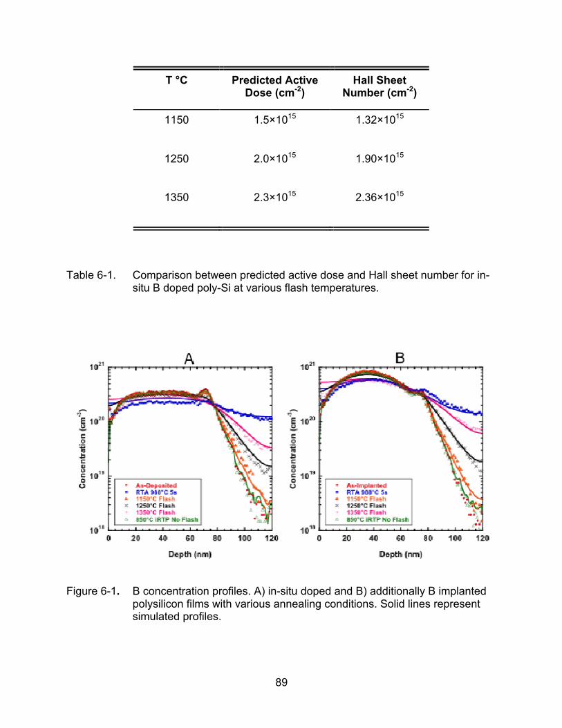
89
T °C Predicted Active Dose (cm-2)
Hall Sheet Number (cm-2)
1150 1.5×10¹⁵ 1.32×10¹⁵
1250 2.0×10¹⁵ 1.90×10¹⁵
1350 2.3×10¹⁵ 2.36×10¹⁵
Table 6-1. Comparison between predicted active dose and Hall sheet number for in-situ B doped poly-Si at various flash temperatures.
Figure 6-1. B concentration profiles. A) in-situ doped and B) additionally B implanted polysilicon films with various annealing conditions. Solid lines represent simulated profiles.
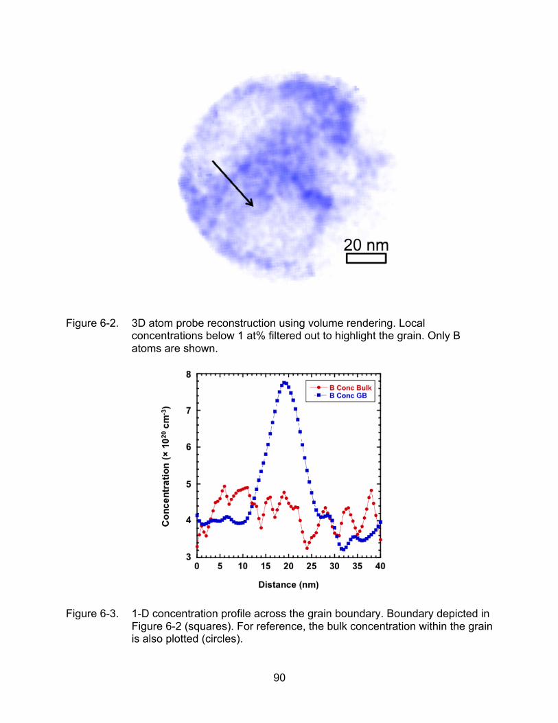
90
Figure 6-2. 3D atom probe reconstruction using volume rendering. Local concentrations below 1 at% filtered out to highlight the grain. Only B atoms are shown.
Figure 6-3. 1-D concentration profile across the grain boundary. Boundary depicted in Figure 6-2 (squares). For reference, the bulk concentration within the grain is also plotted (circles).
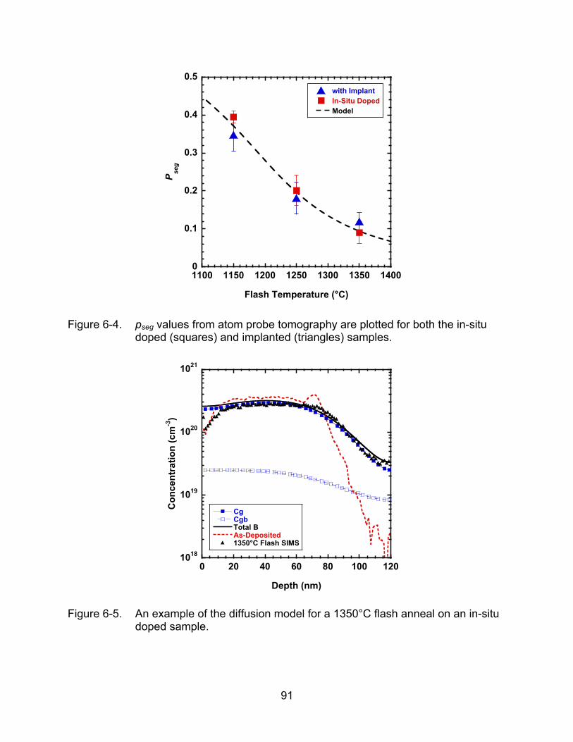
91
0
0.1
0.2
0.3
0.4
0.5
1100 1150 1200 1250 1300 1350 1400
with ImplantIn-Situ DopedModel
P seg
Flash Temperature (°C)
Figure 6-4. pseg values from atom probe tomography are plotted for both the in-situ doped (squares) and implanted (triangles) samples.
1018
1019
1020
1021
0 20 40 60 80 100 120
CgCgbTotal BAs-Deposited1350°C Flash SIMS
Con
cent
ratio
n (c
m-3
)
Depth (nm)
Figure 6-5. An example of the diffusion model for a 1350°C flash anneal on an in-situ doped sample.
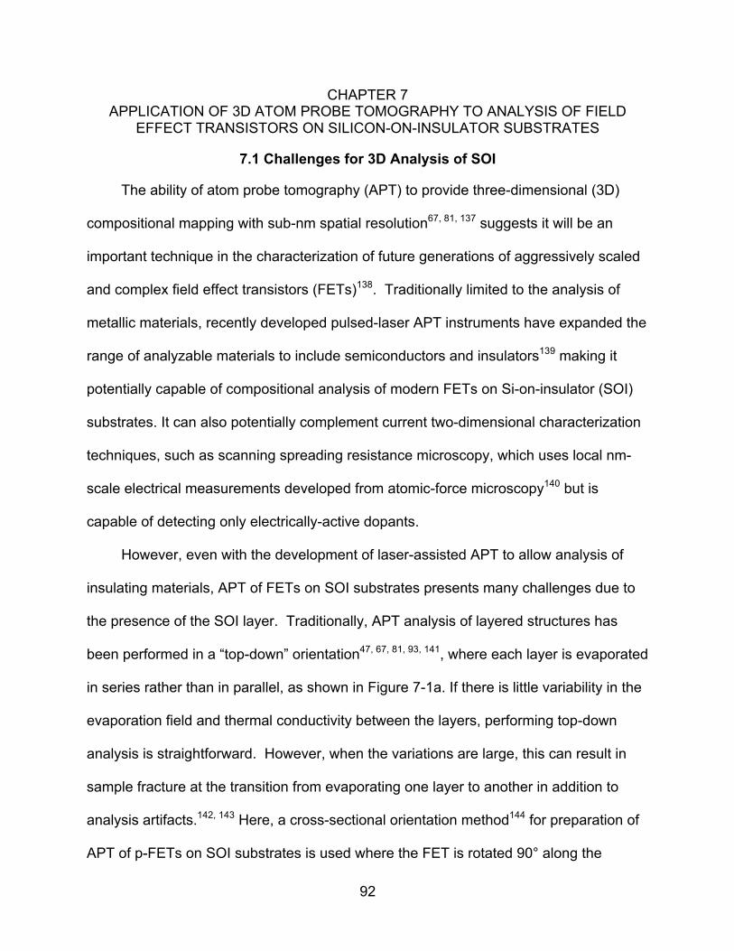
92
CHAPTER 7 APPLICATION OF 3D ATOM PROBE TOMOGRAPHY TO ANALYSIS OF FIELD
EFFECT TRANSISTORS ON SILICON-ON-INSULATOR SUBSTRATES
7.1 Challenges for 3D Analysis of SOI
The ability of atom probe tomography (APT) to provide three-dimensional (3D)
compositional mapping with sub-nm spatial resolution67, 81, 137 suggests it will be an
important technique in the characterization of future generations of aggressively scaled
and complex field effect transistors (FETs)138. Traditionally limited to the analysis of
metallic materials, recently developed pulsed-laser APT instruments have expanded the
range of analyzable materials to include semiconductors and insulators139 making it
potentially capable of compositional analysis of modern FETs on Si-on-insulator (SOI)
substrates. It can also potentially complement current two-dimensional characterization
techniques, such as scanning spreading resistance microscopy, which uses local nm-
scale electrical measurements developed from atomic-force microscopy140 but is
capable of detecting only electrically-active dopants.
However, even with the development of laser-assisted APT to allow analysis of
insulating materials, APT of FETs on SOI substrates presents many challenges due to
the presence of the SOI layer. Traditionally, APT analysis of layered structures has
been performed in a “top-down” orientation47, 67, 81, 93, 141, where each layer is evaporated
in series rather than in parallel, as shown in Figure 7-1a. If there is little variability in the
evaporation field and thermal conductivity between the layers, performing top-down
analysis is straightforward. However, when the variations are large, this can result in
sample fracture at the transition from evaporating one layer to another in addition to
analysis artifacts.142, 143 Here, a cross-sectional orientation method144 for preparation of
APT of p-FETs on SOI substrates is used where the FET is rotated 90° along the
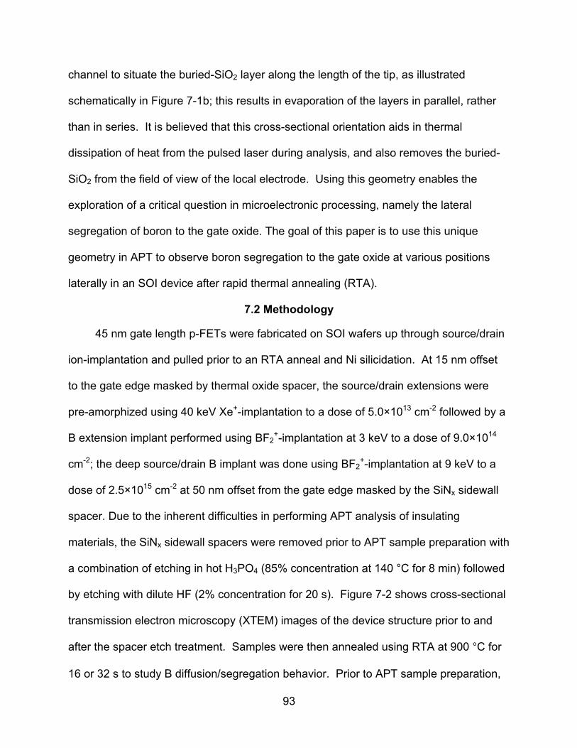
93
channel to situate the buried-SiO2 layer along the length of the tip, as illustrated
schematically in Figure 7-1b; this results in evaporation of the layers in parallel, rather
than in series. It is believed that this cross-sectional orientation aids in thermal
dissipation of heat from the pulsed laser during analysis, and also removes the buried-
SiO2 from the field of view of the local electrode. Using this geometry enables the
exploration of a critical question in microelectronic processing, namely the lateral
segregation of boron to the gate oxide. The goal of this paper is to use this unique
geometry in APT to observe boron segregation to the gate oxide at various positions
laterally in an SOI device after rapid thermal annealing (RTA).
7.2 Methodology
45 nm gate length p-FETs were fabricated on SOI wafers up through source/drain
ion-implantation and pulled prior to an RTA anneal and Ni silicidation. At 15 nm offset
to the gate edge masked by thermal oxide spacer, the source/drain extensions were
pre-amorphized using 40 keV Xe+-implantation to a dose of 5.0×1013 cm-2 followed by a
B extension implant performed using BF2+-implantation at 3 keV to a dose of 9.0×10¹⁴
cm-2; the deep source/drain B implant was done using BF2+-implantation at 9 keV to a
dose of 2.5×1015 cm-2 at 50 nm offset from the gate edge masked by the SiNx sidewall
spacer. Due to the inherent difficulties in performing APT analysis of insulating
materials, the SiNx sidewall spacers were removed prior to APT sample preparation with
a combination of etching in hot H3PO4 (85% concentration at 140 °C for 8 min) followed
by etching with dilute HF (2% concentration for 20 s). Figure 7-2 shows cross-sectional
transmission electron microscopy (XTEM) images of the device structure prior to and
after the spacer etch treatment. Samples were then annealed using RTA at 900 °C for
16 or 32 s to study B diffusion/segregation behavior. Prior to APT sample preparation,
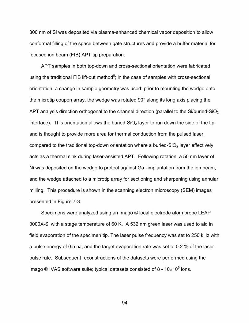
94
300 nm of Si was deposited via plasma-enhanced chemical vapor deposition to allow
conformal filling of the space between gate structures and provide a buffer material for
focused ion beam (FIB) APT tip preparation.
APT samples in both top-down and cross-sectional orientation were fabricated
using the traditional FIB lift-out method8; in the case of samples with cross-sectional
orientation, a change in sample geometry was used: prior to mounting the wedge onto
the microtip coupon array, the wedge was rotated 90° along its long axis placing the
APT analysis direction orthogonal to the channel direction (parallel to the Si/buried-SiO2
interface). This orientation allows the buried-SiO2 layer to run down the side of the tip,
and is thought to provide more area for thermal conduction from the pulsed laser,
compared to the traditional top-down orientation where a buried-SiO2 layer effectively
acts as a thermal sink during laser-assisted APT. Following rotation, a 50 nm layer of
Ni was deposited on the wedge to protect against Ga+-implantation from the ion beam,
and the wedge attached to a microtip array for sectioning and sharpening using annular
milling. This procedure is shown in the scanning electron microscopy (SEM) images
presented in Figure 7-3.
Specimens were analyzed using an Imago © local electrode atom probe LEAP
3000X-Si with a stage temperature of 60 K. A 532 nm green laser was used to aid in
field evaporation of the specimen tip. The laser pulse frequency was set to 250 kHz with
a pulse energy of 0.5 nJ, and the target evaporation rate was set to 0.2 % of the laser
pulse rate. Subsequent reconstructions of the datasets were performed using the
Imago © IVAS software suite; typical datasets consisted of 8 - 10×106 ions.
95
7.3 Results and Discussion
3D APT analysis was attempted for both top-down and cross-sectional samples for
as-implanted samples and samples annealed at 900 °C for 16 s and 32 s. However,
because of specimen tip fracture during analysis, no successful data from top-down
samples were collected. This is indicative of the challenges associated with sequential
field evaporation of layered structures containing insulating materials. Figure 7-4a
presents a reconstructed volume of the gate edge region from an as-implanted cross-
sectional APT sample displaying individual B atoms; an extracted two-dimensional B
concentration contour plot is provided for comparison in Figure 7-4b with an XTEM
micrograph of the same region shown in Figure 7-4c. The two-dimensional contour plot
was generated by assigning color values to concentration ranges within a 1 nm x 1 nm
area.
A small analysis volume of 5 nm × 10 nm × 20 nm at 5 nm from the gate edge was
extracted from the total device reconstruction to examine the segregation of B laterally
to the gate SiO2. The B concentration across the gate SiO2 in this region is plotted at 0.5
nm bin widths in Figure 7-5 for different annealing times at 900 °C; accumulation of B at
the gate SiO2 is clearly evident. The segregation coefficient of boron was calculated to
be ~4, which is slightly below the reported values in the literature at the anneal
temperature used.145, 146 Colby et al. reports a segregation coefficient of 5.1 while
Pfiester et al. estimates a value between 4 and 6 depending on the effective B diffusivity
in the oxide. It is important to note that this segregation not only comes from the poly-Si
gate doping, but the lateral diffusion from the source drain extension implant, which is
observed here directly. This is evidenced by the increasing concentration seen in the
channel region with increasing anneal time. It is difficult to determine the exact

96
mechanism for B accumulation at the gate SiO2. It may be the result of segregation to
the oxidized surface in the implanted region followed by an enhanced lateral diffusion
under the gate through the SiO2145. It is also possible that because B diffuses by an
interstitialcy-kickout mechanism31, and both the implant and anneal conditions are
conducive for transient enhanced diffusion28, this segregation may occur if the B from
the implant diffuses laterally in the silicon and subsequently follows the gradient of
implantation induced interstitials up to the gate oxide. This has been proposed to
explain the so called reverse short channel effect.28, 40 Also, because BF2+ is the
implantation species, the incorporation of F from ion implantation has been shown to
enhance gate oxide penetration145, 147, 148, the diffusivity of boron within the SiO2 has
been shown to be further enhanced as thickness is reduced.147 Prior APT work of
blanket gate electrode poly-Si implanted with B+ instead of BF2+ revealed B diffusing
into the gate oxide46, but no accumulation in nor penetration through the SiO2 was
observed following annealing, suggesting that the presence of F is responsible for the
results seen here.
Diffusion of B from the source/drain extension and deep source/drain implants was
modeled using the Florida Object Oriented Process Simulator (FLOOPS) using a pair
diffusion model, which describes the diffusivity enhancement of B in the presence of a
supersaturated concentration of interstitials generated from the preamorphizing Xe+
implant. The interstitial profile is modeled using SRIM and plotted in Figure 7-6. Only the
implanted areas of the simulated device are given this profile, while masked and
amorphized regions use the equilibrium value Ci*. The interstitials then diffuse to the
surface where they annihilate with a rate known as the surface recombination velocity,

97
ksurf. Reported ksurf values vary over five orders of magnitude149 for the temperature
studied here. A ksurf value of 3×10⁻⁴ s-1 was found to be in good agreement with the
experimental measurement, which is the same value determined by Agarwal and
Dunham150.
This work shows that 3D APT data allows site-specific analysis from commercially
processed devices on SOI wafers when the cross-sectional method is used. However,
it is important to note that the analyzed volume in a 3D device reconstruction is ~106
times smaller than the volume analyzed using conventional secondary ion mass
spectrometry on a blanket SOI wafer; naturally, the dynamic range and sensitivity will be
reduced. However, an additional benefit of using a cross-sectional geometry is that with
a sufficiently high ion count, the B concentration can be averaged through the width of
the gate, therefore producing more accurate data. Nevertheless, there is a set
maximum analysis volume before the tip widens to the point that the buried-SiO2 layer is
in the field of view; it is usually at this point that sample fracture was observed to occur
in samples prepared in cross-sectional orientation.
98
Figure 7-1. Schematic representation comparing two different methods of APT sample orientation of FETs on SOI substrates. A) traditional top-down analysis volume for an atom probe tip centered about the gate. B) cross-sectional orientation.
Figure 7-2. XTEM micrograph of the p-FET structure. A) the as-received structure. B) the structure with SiNx sidewall spacer and thermal SiO2 spacer removed after hot H3PO4 and dilute HF etching.

99
Figure 7-3. SEM micrographs of APT sample preparation via FIB milling. A) an in-situ micromanipulator removes an ion-milled wedge from an array of p-FETs, B) the wedge is rotated 90° about the long axis (so the analysis direction lies within the plane of the Si/buried-SiO2 interface and is perpendicular to the channel direction) coated with ~50 nm of Ni, and mounted/sectioned to a Si microtip. C) the tip is sharpened into final shape via annular milling.
Figure 7-4. 3D Reconstruction of as-implanted p-FET. A) 3D analysis cone rotated to show the B extension implant (red) next to the gate; 5% Si ions shown (Grey). B) 2D contour plot showing concentration values for the B extension implant. C) XTEM micrograph from the same area of the device. An analysis volume outlines the location of the extracted 1D concentration profile.
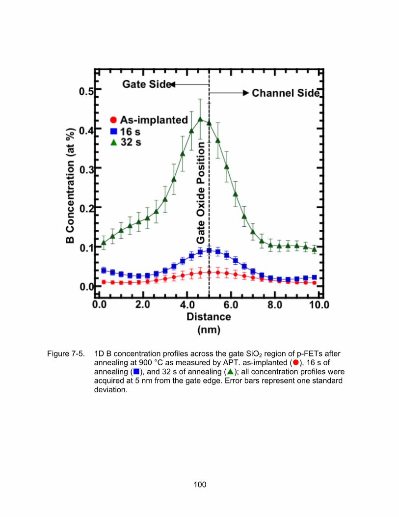
100
Figure 7-5. 1D B concentration profiles across the gate SiO2 region of p-FETs after annealing at 900 °C as measured by APT. as-implanted (), 16 s of annealing (), and 32 s of annealing (); all concentration profiles were acquired at 5 nm from the gate edge. Error bars represent one standard deviation.
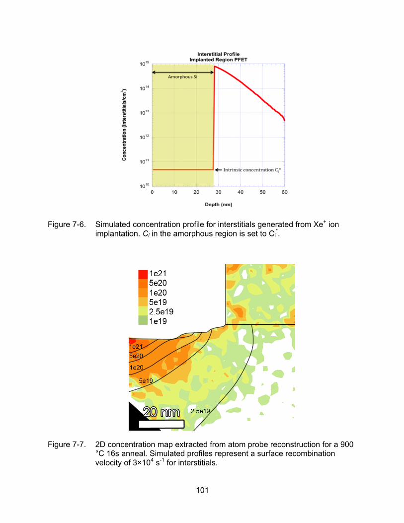
101
Figure 7-6. Simulated concentration profile for interstitials generated from Xe+ ion implantation. Ci in the amorphous region is set to Ci
*.
Figure 7-7. 2D concentration map extracted from atom probe reconstruction for a 900 °C 16s anneal. Simulated profiles represent a surface recombination velocity of 3×10⁴ s-1 for interstitials.

102
CHAPTER 8 CONCLUSIONS AND FUTURE WORK
In this work, flash-assist rapid thermal annealing was used in order to explore the
diffusion behavior of B in poly-Si. One of the most controversial questions was whether
or not B segregated to the grain boundaries. This type of segregation behavior, already
seen for the n-type dopants As and P, is incredibly important with regard to
microelectronics processing. First, segregated B is not electrically active, and therefore
brings down the expected conductivity of the material. Secondly, diffusion in grain
boundaries is known to be much faster than in the bulk. Understanding segregation
behavior is crucial to modeling diffusion behavior in poly-Si. It was shown that B does
indeed segregate to the grain boundaries under specific thermal conditions, such as
flash annealing, which allowed creation of a highly active film with limited grain growth,
creating the perfect environment for segregation to occur. The scale of this
microstructure was then able to be analyzed using three-dimensional tomographic
analytical techniques such as atom probe tomography, which has a limited field of view
on the order of 150 nm.
Through the use of transmission electron microscopy, secondary ion mass
spectrometry, three-dimensional atom probe tomography as well as Hall effect, a
comprehensive model was developed to describe microstructural, electrical, and
diffusion behavior of heavily B doped poly-Si films under flash annealing conditions. The
results are able to confirm the segregation of B to grain boundaries during flash
annealing, while also validating previous work by other groups where segregation was
not seen due to longer anneals with noticeable grain growth, which reduces segregation
significantly.

103
Since the majority of the work shown here was done on bulk thin films, the natural
progression for research would be to extend 3D APT to actual production devices. Due
to instrument limitations at the time of this work, 3D APT had not yet evolved to where
analysis of insulating oxides was straightforward. New tools have since been developed
that are much more capable in this regard and can make analysis of production devices
a possibility without deprocessing of various insulating device structures and relayering
with compatible material.

104
APPENDIX A FLOOPS SIMULATION CODE FOR B DIFFUSION IN POLY-SI
Included here is the simulation code used in FLOOPS in order to simulate the
diffusion profiles from Chapter 6. Values to be edited based on experimental
parameters are noted in [ ] brackets.
#FLOOPS B Poly-Si Diffusion math diffuse dim=1 umf none col scale #Bg = B concentration within the grain Bb = B concentration in grain boundary solution add name=Bg solve !negative solution add name=Bb solve !negative #Creates structure of 120 nm Si on 12 nm of Oxide on top of 1 micron of Si line x loc=0.0 spac=0.001 tag=Top line x loc=0.12 spac=0.001 tag=Oxidetop line x loc=.132 spac=0.001 tag=Oxidebottom line x loc=1.0 spac=0.01 tag=Bottom region silicon xlo=Top xhi=Oxidetop region oxide xlo=Oxidetop xhi=Oxidebottom region silicon xlo=Oxidebottom xhi=Bottom init #Inputs the SIMS profile, in this case, the as-implanted profile. profile name=Boron inf=[as-imp.csv] xscale=1e-3 sel z=1e16+Boron name=Bg sel z=1.0e10 name=Bb sel z=log10(Bg) #Plots and labels the initial grain and grain boundary profiles plot.1d label= "Bg0" sel z=log10(Bb) plot.1d !cle label= "Bb0" #Diffusion is modeled in three parts: ramp up, flash, and ramp down #This next line defines the kinetic reaction term using values calculated for 850 °C pre-#flash temperature set Gen "(Bg*[pseg(850°C)] - Bb) * $tau” #This line defines τ-1 set tau "6.12e22*exp(-5.76/(8.62e-5*(Temp+273)))"
105
pdbSetString Si Bg Equation "ddt(Bg)-(0.37*exp(-3.46/(8.62e-5*(Temp+273)))+[p/ni(850°C)]*0.76*exp(-3.46/(8.62e-5*(Temp+273)))*grad(Bg) + $Gen" pdbSetString Si Bb Equation "ddt(Bb)-0.012*exp(-1.95/(8.62e-5*(Temp+273))))*grad(Bb) - $Gen" rta start.temp=[20] ramp=[150] cool=1e6 dwell.temp=[850] dwell.time=0 #Diffusion during the flash is modeled here with a 1 ms pulse duration. set Gen "(Bg*[pseg(Tflash)] - Bb) * $tau" pdbSetString Si Bg Equation "ddt(Bg)-(0.37*exp(-3.46/(8.62e-5*(Temp+273)))+[p/ni(Tflash)]*0.76*exp(-3.46/(8.62e-5*(Temp+273))))*grad(Bg) + $Gen" pdbSetString Si Bb Equation "ddt(Bb)-0.012*exp(-1.95/(8.62e-5*(Temp+273)))*grad(Bb) - $Gen" rta start.temp=850 ramp=1e6 cool=[cooling rate] dwell.temp= [Tflash] dwell.time=[.001] #Ramp down is modeled here, starting at 950 °C, and cooling at 125 °C/s. Initial ramp #down temperature changes with flash temperature. set Gen "(Bg*pseg(950°C) - Bb) * $tau" pdbSetString Si Bg Equation "ddt(Bg)-(0.37*exp(-3.46/8.62e-5*(Temp+273)))+[p/ni(950°C)]*0.76*exp(-3.46/(8.62e-5*(Temp+273))))*grad(Bg) + $Gen" pdbSetString Si Bb Equation "ddt(Bb)-0.012*exp(-1.95/(8.62e-5*(Temp+273)))*grad(Bb) - $Gen" rta start.temp=949 ramp=150 cool=[100] dwell.temp=950 dwell.time=0 #plots the output sel z=log10(Bg) plot.1d !cle label = "Bgfin" sel z=log10(Bb) plot.1d !cle label= "Bbfin"

106
APPENDIX B FLOOPS SIMULATION CODE FOR 2D B DIFFUSION OF SOURCE DRAIN
EXTENSION IN P-MOSFET ON SOI
Included here is the FLOOPS simulation code used in Chapter 7 in order to obtain
the simulated concentration contours used in Figure 7-7 for diffusion of B from the
source-drain extension and source-drain implants.
#FLOOPS B Source Drain Diffusion #Grid initialization – 2 nm gate oxide on 60 nm Si, 100 nm Buried oxide, on Si line x loc=-0.002 tag=gate_ox spa=0.002 line x loc=0.0 tag=top spa=0.002 line x loc=0.06 tag=ox_top spa=0.002 line x loc=0.16 tag=ox_bottom spac=0.01 line x loc=0.5 tag=bot spa=0.05 line y loc=0.0 tag=left spa=0.002 line y loc=0.1 tag=right spa=0.002 region silicon xlo=top xhi=ox_top ylo=left yhi=right region oxide xlo=ox_top xhi=ox_bottom ylo=left yhi=right region oxide xlo=gate_ox xhi=top ylo=left yhi=right region silicon xlo=ox_bottom xhi=bot ylo=left yhi=right init #Mask for source drain extension implant mask clear mask name=extension left=-0.1 right=0.04 #etch oxide rate=0.002 time=1 spac=0.002 aniso mask=extension #Extension Implant using BF2 9e14 3kv implant bf2 energy=3 dose=9e14 mask=extension #Mask for deep source drain implant mask clear mask name=sd left=-0.1 right=0.066 #Deep Source-Drain Implant using BF2 2.5e15 9kV implant bf2 energy=9 dose=2.5e15 mask=sd sel z=1e17+Boron name=Boron #Creates profile of interstitials from the Xe preamorphization implant (40 kV 5e13) profile name=Int inf=[Intprofile.csv] xscale=1e-4
107
#math diffuse dim=1 umf none triplet pdbSetSwitch Si I DiffModel Numeric pdbSetSwitch Si V DiffModel Numeric # Int diffusion after Ural et al. PRL 83 (1999) p3454 #pdbSetDouble Silicon Int D0 {[Arrhenius 5.54e-3 0.85]} pdbSetDouble Silicon Int Cstar {[Arrhenius [expr 5.0e22*exp(10.2)] 3.83]} pdbSetDouble Silicon Vac D0 {[Arrhenius 1.756e-3 0.493]} pdbSetDouble Silicon Vac Cstar {[Arrhenius [expr 5.0e22*exp(12.8)] 4.367]} pdbSetSwitch Silicon Boron DiffModel Pair pdbSetSwitch Silicon Boron ActiveModel None pdbSetDouble Silicon Boron Int Binding {[Arrhenius 8.0e-23 -1.50]} pdbSetDouble Silicon Boron Vac Binding {[Arrhenius 8.0e-23 -0.00]} pdbSetDouble Oxide_Silicon Vac Ktrap 0.00 pdbSetDouble Oxide_Silicon Int Ktrap 0.00 #Sets KSurf, the surface recombination variable at the oxide interface. pdbSetDouble Oxide_Silicon Int Ksurf [Ksurf value] sel z=900 name=Temp #Sets implanted areas beyond amorphous crystalline interface to interstitial profile from #Xe implant plus Ci and Cv values for 900 °C sel z=(y>0.04)*(x>0.028)*Int+4.726e10 name=Int sel z=3.12e9 name=Vac sel z=log10(Boron); #Let FLOOPS set correct equilibrium variables diffuse time=1e-15 temp=900 sel z=EqInt+Int name=Int sel z=EqVac+Vac name=Vac #Anneal for 16s at 900 °C diffuse time=0.267 temp=900 #2D Plot plot.2d grid sel z=Boron contour val=1e21 contour val=5e20 contour val=1e20 contour val=5e19 contour val=2.5e19 contour val=1e19
108
LIST OF REFERENCES
1G. Moore, in Electronics Magazine (1965). 2D. L. Anderson, Science 243, 367 (1989). 3G. L. Pearson and J. Bardeen, Phys. Rev. 75, 865 (1949). 4J. S. Liu, C. H. Kuan, S. C. Cha, W. L. Chuang, G. J. Gau and J. Y. Jeng, Sol. Energy Mater. Sol. Cells 95, 3130 (2011). 5H. Rücker, B. Heinemann, R. Barth, D. Knoll, P. Schley, R. Scholz, B. Tillack and W. Winkler, Materials Science in Semiconductor Processing 8, 279 (2005). 6F. Faggin and T. Klein, Solid-State Electron. 13, 1125 (1970). 7D. Bolze, B. Heinemann, J. Gelpey, S. McCoy and W. Lerch, 1 (2009). 8T. Gebel, M. Voelskow, W. Skorupa, G. Mannino, V. Privitera, F. Priolo, E. Napolitani and A. Carnera, Nucl. Instrum. Methods B 186, 287 (2002). 9V. E. Borisenko and S. G. Yudin, Phys. Status Solidi A-Appl. Res. 101, 123 (1987). 10D. Camm, J. Gelpey, T. Thrum, G. Stuart and S. McCoy, JOM Journal of the Minerals, Metals and Materials Society 58, 32 (2006). 11R. E. Hummel, Electronic Properties of Materials. (Springer, New York, 2001). 12D. Briand, M. Sarret, K. Kis-Sion, T. Mohammed-Brahim and P. Duverneuil, Semicond. Sci. Technol. 14, 173 (1999). 13H. Kuhne, A. Fischer, M. C. Ozturk and M. K. Sanganeria, J. Electrochem. Soc. 143, 634 (1996). 14J. Puigdollers, J. Cifre, M. C. Polo, J. M. Asensi, J. Bertomeu, J. Andreu and A. Lloret, Appl. Surf. Sci. 86, 600 (1995). 15P. Rai-Choudhury and P. L. Hower, J. Electrochem. Soc. 120, 1761 (1973). 16K. S. Jones, S. Prussin and E. R. Weber, Appl. Phys. A-Mater. Sci. Process. 45, 1 (1988). 17W. Bohmayr, A. Burenkov, J. Lorenz, H. Ryssel and S. Selberherr, IEEE Trans. Comput.-Aided Design Integr. Circuits Syst 17, 1236 (1998). 18J. Narayan, J. Vac. Sci. Technol. A 2, 1303 (1984). 19J. Washburn, C. S. Murty, D. Sadana, P. Byrne, R. Gronsky, N. Cheung and R. Kilaas, Nuclear Instruments & Methods in Physics Research 209, 345 (1983). 20O. W. Holland, T. P. Sjoreen, D. Fathy and J. Narayan, Appl. Phys. Lett. 45, 1081 (1984). 21M. Aboy, Appl. Phys. Lett. 88, 191917 (2006). 22M. Aboy, L. Pelaz, J. Barbolla, R. Duffy and V. C. Venezia, Mat. Sci. Eng. B 124, 205 (2005). 23K. Suzuki, H. Tashiro, K. Narita and Y. Kataoka, IEEE Trans. Electron Devices 51, 663 (2004). 24L. Csepregi, E. F. Kennedy, J. W. Mayer and T. W. Sigmon, J. Appl. Phys. 49, 3906 (1978). 25J. M. Poate and J. S. Williams, Ion Implantation and Beam Processing. (Academic Press, New York, 1984). 26K. S. Jones and D. Venables, J. Appl. Phys. 69, 2931 (1991). 27D. J. Eaglesham, P. A. Stolk, H. J. Gossmann and J. M. Poate, Appl. Phys. Lett. 65, 2305 (1994).
109
28C. Bonafos, M. Omri, B. de Mauduit, G. BenAssayag, A. Claverie, D. Alquier, A. Martinez and D. Mathiot, J. Appl. Phys. 82, 2855 (1997). 29S. Nedelec, D. Mathiot and M. Gauneau, presented at the Solid State Device Research Conference, 1996. ESSDERC '96. Proceedings of the 26th European, 1996 (unpublished). 30J. Foggiato, J. Vac. Sci. Technol. B 24, 515 (2006). 31P. M. Fahey, P. B. Griffin and J. D. Plummer, Rev. Mod. Phys. 61, 289 (1989). 32H. Zimmermann and H. Ryssel, Phys. Rev. B 44, 9064 (1991). 33H. J. Gossmann, Electrochem. Soc. Proc. 98 (1998). 34P. A. Stolk, H. J. Gossmann, D. J. Eaglesham and J. M. Poate, Nucl. Instrum. Methods B 96, 187 (1995). 35R. Lever, J. Appl. Phys. 78, 3115 (1995). 36L. Shao, J. Liu, Q. Y. Chen and W.-K. Chu, Mat. Sci. Eng. R 42, 65 (2003). 37A. Ural, P. B. Griffin and J. D. Plummer, Phys. Rev. Lett. 83, 3454 (1999). 38D. R. Lim, C. S. Rafferty and F. P. Klemens, Appl. Phys. Lett. 67, 2302 (1995). 39H. Gossmann, Appl. Phys. Lett. 67, 1558 (1995). 40C. S. Rafferty, Vuong, H.-H, Eshraghi, S. A., Giles, M. D., Pinto, M. R., Hillenius, S. J., IEDM 93, 311 (1993). 41D. De Salvador, Appl. Phys. Lett. 87, 221902 (2005). 42A. H. King and D. A. Smith, Philos. Mag. A-Phys. Condens. Matter Struct. Defect Mech. Prop. 42, 495 (1980). 43S. Hu, Appl. Phys. Lett. 51, 308 (1987). 44S. Herner, Appl. Phys. Lett. 72, 2289 (1998). 45M. Mandurah, J. Appl. Phys. 51, 5755 (1980). 46K. Inoue, F. Yano, A. Nishida, H. Takamizawa, T. Tsunomura, Y. Nagai and M. Hasegawa, Appl. Phys. Lett. 95 (2009). 47K. Thompson, J. H. Bunton, T. F. Kelly and D. J. Larson, Journal of Vacuum Science & Technology B: Microelectronics and Nanometer Structures 24, 421 (2006). 48K. Suzuki, N. Miyata and K. Kawamura, Jap. J. of Appl. Phys. 34, 1748 (1995). 49M. Y. Ghannam and R. W. Dutton, Appl. Phys. Lett. 52, 1222 (1988). 50S. Abadli and F. Mansour, presented at the Microelectronics, 2004. ICM 2004 Proceedings. The 16th International Conference on, 2004 (unpublished). 51B. J. Mulvaney, W. B. Richardson and T. L. Crandle, IEEE Trans. Comput-Aided Des. Integr. Circuits Syst. 8, 336 (1989). 52L. Mei and R. W. Dutton, IEEE Trans. Electron Devices 29, 1726 (1982). 53M. Mandurah, Appl. Phys. Lett. 36, 683 (1980). 54N. C. C. Lu, L. Gerzberg and J. D. Meindl, Elec. Dev. Lett. 1, 38 (1980). 55G. Mannino, Appl. Phys. Lett. 78, 889 (2001). 56D. M. Camm and B. Loject, presented at the 2nd Int. Conf. Advanced Thermal Processing of Semiconductors, 1994 (unpublished). 57J. Y. W. Seto, J. Appl. Phys. 46, 5247 (1975). 58T. I. Kamins, J. Appl. Phys. 42, 4357 (1971). 59Y. Kumar and P. C. Mathur, Phys. Lett. A 119, 361 (1987). 60F. A. Trumbore, Bell System Technical Journal 39, 205 (1960). 61L. J. Van der Pauw, Phillips Technical Review 20, 220 (1958). 62L. J. Van der Pauw, Philips Res. Repts. 13, 1 (1958).

110
63J. F. Lin, S. S. Li, L. C. Linares and K. W. Teng, Solid-State Electron. 24, 827 (1981). 64S. S. Li and W. R. Thurder, Solid-State Electron. 20, 609 (1977). 65C. W. Magee and M. R. Frost, Int. J. Mass Spectom. Ion Process. 143, 29 (1995). 66W. Vandervorst and T. Clarysse, J. Vac. Sci. Technol. B 10, 302 (1992). 67S. Koelling, M. Gilbert, J. Goossens, A. Hikavyy, O. Richard and W. Vandervorst, Appl. Phys. Lett. 95, 144106 (2009). 68C. W. Magee, R. S. Hockett, T. H. Buyuklimanli, I. Abdelrehim and J. W. Marino, Nucl. Instrum. Methods B 261, 594 (2007). 69T. T. Tsong, (Cambridge University Press, 1990). 70E. Müller, Z. Physik 131, 136 (1951). 71D. N. Seidman, Ann. Rev. Mater. Res. 37 (2007). 72B. Gault, F. Vurpillot, A. Bostel, A. Menand and B. Deconihout, Appl. Phys. Lett. 86 (2005). 73E. Müller and K. Bahadur, Phys. Rev. 102, 624 (1956). 74E. Müller, Phys. Rev. 102: 618-24 (1956). 75E. Müller, J. Panitz and S. Mclane, Rev. Sci. Instrum. 39, 83 (1968). 76J. Panitz, Rev. Sci. Instrum. 44 (1973). 77A. Cerezo, T. Godfrey and G. D. W. Smith, Rev. Sci. Instrum. 59 (1988). 78T. F. Kelly, P. P. Camus, D. J. Larson, L. Holzman and S. Bajikar, Ultramicroscopy 62, 29 (1996). 79M. Miller, A. Cerezo, M. Hetherington and G. D. W. Smith, (Oxford Univ. Press, Oxford, UK, 1996). 80T. F. Kelly, in International Conference on Frontiers of Characterization and Metrology for Nanoelectronics (2007). 81T. F. Kelly, D. J. Larson, K. Thompson, R. L. Alvis, J. H. Bunton, J. D. Olson and B. P. Gorman, Ann. Rev. Mater. Res. 37, 681 (2007). 82J. H. Bunton, J. D. Olson, D. R. Lenz and T. E. Kelly, Microsc. Microanal. 13, 418 (2007). 83M. Tsukada, H. Tamura, K. P. McKenna, A. L. Shluger, Y. M. Chen, T. Ohkubo and K. Hono, Ultramicroscopy 111, 567 (2011). 84Y. M. Chen, T. Ohkubo and K. Hono, Ultramicroscopy 111, 562 (2011). 85K. Hono, T. Ohkubo, Y. M. Chen, M. Kodzuka, K. Oh-ishi, H. Sepehri-Amin, F. Li, T. Kinno, S. Tomiya and Y. Kanitani, Ultramicroscopy 111, 576 (2011). 86C. Oberdorfer, P. Stender, C. Reinke and G. Schmitz, Microsc. Microanal. 13, 342 (2007). 87K. Thompson, J. H. Booske, D. J. Larson and T. F. Kelly, Appl. Phys. Lett. 87 (2005). 88K. Inoue, F. Yano, A. Nishida, T. Tsunomura, T. Toyama, Y. Nagai and M. Hasegawa, Appl. Phys. Lett. 92, 103506 (2008). 89K. Thompson, P. L. Flaitz, P. Ronsheim, D. J. Larson and T. F. Kelly, Science 317, 1370 (2007). 90S. Duguay, Appl. Phys. Lett. 97, 242104 (2010). 91O. Cojocaru-Miredin, D. Mangelinck and D. Blavette, J. Appl. Phys. 106 (2009). 92O. Cojocaru-MirÈdin, E. Cadel, F. Vurpillot, D. Mangelinck and D. Blavette, Scripta Materialia 60, 285 (2009). 93J. S. Moore, K. S. Jones, H. Kennel and S. Corcoran, Ultramicroscopy 108, 536 (2008).
111
94M. R. Holzworth, N. G. Rudawski, S. J. Pearton, K. S. Jones, L. Lu, T. S. Kang, F. Ren and J. W. Johnson, Appl. Phys. Lett. 98 (2011). 95M. Gilbert, W. Vandervorst, S. Koelling and A. K. Kambham, Ultramicroscopy 111, 530 (2011). 96A. K. Kambham, J. Mody, M. Gilbert, S. Koelling and W. Vandervorst, Ultramicroscopy 111, 535 (2011). 97K. Thompson, D. Lawrence, D. J. Larson, J. D. Olson, T. F. Kelly and B. Gorman, Ultramicroscopy 107, 131 (2007). 98L. de Broglie, Foundations of Physics 1, 5 (1970). 99M. S. Kulkarni and H. F. Erk, J. Electrochem. Soc. 147, 176 (2000). 100L. A. Giannuzzi, J. L. Drown, S. R. Brown, R. B. Irwin and F. Stevie, Microsc. Res. Tech. 41, 285 (1998). 101L. Mei, M. Rivier, Y. Kwark and R. W. Dutton, J. Electrochem. Soc. 129, 1791 (1982). 102S. Kalainathan, R. Dhanasekaran and P. Ramasamy, J. Elec. Mat. 19, 1135 (1990). 103S. Kalainathan, R. Dhanasekaran and P. Ramasamy, J. Mat. Sci.: Mat. in Elec. 2, 98 (1991). 104H. J. Kim and C. V. Thompson, J. Electrochem. Soc. 135, 2312 (1988). 105H. Kim, J. Appl. Phys. 67, 757 (1990). 106C. V. Thompson, J. Appl. Phys. 58, 763 (1985). 107C. V. Thompson, Interface Sci. 6, 85 (1998). 108A. R. Sitaram, Murarka, S. P., Sheng, T. T., J. Mat. Res. 5, 360 (1990). 109H. J. Kim and C. V. Thompson, Appl. Phys. Lett. 48, 399 (1986). 110H. A. Atwater, C. V. Thompson and H.-J. Kim, Nucl. Instrum. Methods B 39, 64 (1989). 111J. Akhtar, S. K. Lamichhane and P. Sen, Materials Science in Semiconductor Processing 8, 476 (2005). 112T. Makino and H. Nakamura, Solid-State Electron. 24, 49 (1981). 113S. P. Chen, J. D. Kress, A. F. Voter and R. C. Albers, presented at the Electrochemical Society Proceedings, 1996 (unpublished). 114B. Masters, Appl. Phys. Lett. 8, 280 (1966). 115C. Seager, Ann. Rev. Mater. Sci. 15, 271 (1985). 116W. Wijaranakula, Appl. Phys. Lett. 65, 2069 (1994). 117W. Lerch, S. Paul, J. Niess, S. McCoy, J. Gelpey, D. Bolze, F. Cristiano, F. Severac, P. Fazzini, A. Martinez and P. Pichler, presented at the 15th annual IEEE International Conference on Advanced Thermal Processing of Semiconductors, Catania, Italy, 2007 (unpublished). 118K. R. C. Mok, S. H. Yeong, B. Colombeau, F. Benistant, C. H. Poon, L. Chan and M. P. Srinivasan, Mat. Sci. Eng. B 154-155, 14 (2008). 119J. Sharp, N. Cowern, R. Webb and K. Kirby, Appl. Phys. Lett. 89, 192105 (2006). 120S. H. Yeong, B. Colombeau, C. H. Poon, K. R. C. Mok, A. See, F. Benistant, D. X. M. Tan, K. L. Pey, C. M. Ng, L. Chan and M. P. Srinivasan, J. Electrochem. Soc. 155, H508 (2008). 121Heleskiv.J and T. Salo, J. Appl. Phys. 43, 740 (1972). 122J. Volger, Phys. Rev. 79, 1023 (1950). 123J. Jerhot and V. Snejdar, Thin Solid Films 52, 379 (1978).
112
124C. H. Poon, A. See, Y. Tan, M. Zhou and D. Gui, J. Electrochem. Soc. 155, H59 (2008). 125S. H. Jain, P. B. Griffin, J. D. Plummer, S. McCoy, J. Gelpey, T. Selinger and D. F. Downey, J. Appl. Phys. 96, 7357 (2004). 126R. A. Camillo-Castillo, M. E. Law and K. S. Jones, J. Appl. Phys. 96, 4939 (2004). 127R. Camillo-Castillo, University of Florida, 2006. 128D. J. Cummings, A. F. Witulski, P. Hyunwoo, R. D. Schrimpf, S. E. Thompson and M. E. Law, Nuclear Science, IEEE Transactions on 57, 2318 (2010). 129G. Masetti, M. Severi and S. Solmi, IEEE Trans. Electron Devices 30, 764 (1983). 130L. Carnel, I. Gordon, D. Van Gestel, G. Beaucarne and J. Poortmans, Thin Solid Films 516, 6839 (2008). 131M. L. Taheri, J. T. Sebastian, B. W. Reed, D. N. Seidman and A. D. Rollett, Ultramicroscopy 110, 278 (2010). 132W. Hosford, (Cambridge University Press, 2007). 133Y. Komem and I. W. Hall, J. Appl. Phys. 52, 6655 (1981). 134M. E. Law and S. M. Cea, Comput. Mater. Sci. 12, 289 (1998). 135R. B. Fair and P. N. Pappas, J. Electrochem. Soc. 122, 1241 (1975). 136C. D. Thurmond, J. Electrochem. Soc. 122, 1133 (1975). 137B. Gault, M. P. Moody, F. de Geuser, D. Haley, L. T. Stephenson and S. P. Ringer, Appl. Phys. Lett. 95 (2009). 138H. S. Bennet, J. Res. Natl. Stand. Technol. 112, 25 (2007). 139Y. M. Chen, T. Ohkubo, M. Kodzuka, K. Morita and K. Hono, Scripta Mater. 61, 693 (2009). 140W. Vandervorst, Appl. Surf. Sci. 255, 805 (2008). 141B. P. Gorman, A. G. Norman and Y. Yan, Microsc. Microanal. 13, 493 (2007). 142B. Gault, A. La Fontaine, M. P. Moody, S. P. Ringer and E. A. Marquis, Ultramicroscopy 110, 1215 (2010). 143A. Shariq, S. Mutas, K. Wedderhoff, C. Klein, H. Hortenbach, S. Teichert, P. Kucher and S. S. A. Gerstl, Ultramicroscopy 109, 472 (2009). 144D. Lawrence, R. L. Alvis and J. D. Olson, Microsc. Microanal. 14, 1004 (2008). 145J. R. Pfiester, L. C. Parrillo and F. K. Baker, IEEE Electron Device Lett. 11, 247 (1990). 146J. W. Colby and L. E. Katz, J. Electrochem. Soc. 123, 409 (1976). 147T. Aoyama, K. Suzuki, H. Tashiro, Y. Toda, T. Yamazaki, K. Takasaki and T. Ito, J. Appl. Phys. 77, 417 (1995). 148J. R. Pfiester, F. K. Baker, T. C. Mele, H. H. Tseng, P. J. Tobin, J. D. Hayden, J. W. Miller and L. C. Parrillo, IEEE Trans. Electron Devices 37, 1842 (1990). 149P. Pichler, Intrinsic point defects, impurities, and their diffusion in silicon. (Springer, 2004). 150A. Agarwal, Appl. Phys. Lett. 74, 2435 (1999).
113
BIOGRAPHICAL SKETCH
Sidan Jin was originally born in Shang-hai, China. He immigrated with his family to
America at the age of two and grew up in Miami, FL. He graduated from Miami Killian
Senior High School and went on to devote the next nine years of his life as a Florida
Gator. He graduated in 2006 with a Bachelor of Science in Materials Science and
Engineering, and decided to continue on with his graduate education at the University of
Florida and received his Master of Science in 2007. While pursuing his Ph. D. under the
advisement of Kevin Jones, Sidan worked on 3D characterization of transistors through
a collaboration with IBM and the Semiconductor Research Corporation (SRC). He
completed an internship with IBM’s East Fishkill facility in 2008 in order to familiarize
himself with 3D analysis using the local electrode atom probe. He went on to continue a
second project with IBM involving flash-assisted rapid thermal annealing of poly-Si films
for heterojunction bipolar applications. After graduating with his Ph. D, he will be joining
Intel Corporation in Chandler, AZ.