Large noble metal clusters: electron confinement and band
15
OPEN ACCESS Large noble metal clusters: electron confinement and band structure effects To cite this article: H Hövel and I Barke 2003 New J. Phys. 5 31 View the article online for updates and enhancements. You may also like Confinement properties of 2D porous molecular networks on metal surfaces Kathrin Müller, Mihaela Enache and Meike Stöhr - Long-range Rydberg–Rydberg interactions in calcium, strontium and ytterbium C L Vaillant, M P A Jones and R M Potvliege - Spin wave surface states in 1D planar magnonic crystals J Rychy and J W Kos - Recent citations The Features of the Electron Exchange of Ions with Metal Nanoclusters I. K. Gainullin - Dynamical resonant neutralization of low- energy Na+ ions scattered from Au(111), Pd(111), Cu(111), and Cu(110) surfaces Lei Gao et al - Electron Transfer Processes on Supported Au Nanoclusters and Nanowires and Substrate Effects Jie Shen et al - This content was downloaded from IP address 118.137.224.51 on 11/11/2021 at 16:57
Transcript of Large noble metal clusters: electron confinement and band

OPEN ACCESS
Large noble metal clusters: electron confinementand band structure effectsTo cite this article: H Hövel and I Barke 2003 New J. Phys. 5 31
View the article online for updates and enhancements.
You may also likeConfinement properties of 2D porousmolecular networks on metal surfacesKathrin Müller, Mihaela Enache and MeikeStöhr
-
Long-range Rydberg–Rydberg interactionsin calcium, strontium and ytterbiumC L Vaillant, M P A Jones and R MPotvliege
-
Spin wave surface states in 1D planarmagnonic crystalsJ Rychy and J W Kos
-
Recent citationsThe Features of the Electron Exchange ofIons with Metal NanoclustersI. K. Gainullin
-
Dynamical resonant neutralization of low-energy Na+ ions scattered from Au(111),Pd(111), Cu(111), and Cu(110) surfacesLei Gao et al
-
Electron Transfer Processes on SupportedAu Nanoclusters and Nanowires andSubstrate EffectsJie Shen et al
-
This content was downloaded from IP address 118.137.224.51 on 11/11/2021 at 16:57

Large noble metal clusters: electron confinementand band structure effects
H Hovel1 and I BarkeUniversity of Dortmund, Experimentelle Physik I, D-44221 Dortmund,GermanyE-mail: [email protected]
New Journal of Physics 5 (2003) 31.1–31.14 (http://www.njp.org/)Received 3 December 2002Published 9 April 2003
Abstract. For the electronic properties of large clusters the interaction of thefree electron gas with the ion core lattice may result in additional quantizationphenomena which are well known in the area of surface and thin-film physics. Wemeasured the geometric and electronic properties of silver and gold clusters grownin nanopits on graphite with low-temperature scanning tunnelling microscopyand spectroscopy in combination with high-resolution photoemission. With theemergence of a Shockley surface state on the top (111) facets of gold clusters witha size of about 104 atoms, we observed one explicit example for the influenceof the ion core lattice. The two-dimensional confinement of the surface stateis set into the context of a possible one-dimensional confinement perpendicularto the surface, analogous to quantum well states in thin metal films. The basicmechanisms for the dependence of the electronic structure on the cluster size andthe shape are tentatively discussed within a ‘bulk limit’, introducing the bulk bandstructure into the description of the clusters.
1 Author to whom any correspondence should be addressed.
New Journal of Physics 5 (2003) 31.1–31.14 PII: S1367-2630(03)57052-51367-2630/03/000031+14$30.00 © IOP Publishing Ltd and Deutsche Physikalische Gesellschaft

31.2
Contents
1. Introduction 22. Experimental details 23. STM and STS results 34. Confined surface states 45. Electron confinement in the cluster volume 106. Band structure effects in the energy quantization 117. Conclusion 12Acknowledgment 13References 13
1. Introduction
There are two possible pathways to approach the properties of clusters, being located betweensingle atoms and the macroscopic bulk material. One can treat them as aggregates of atoms, i.e.large molecules, or one can describe them as a nanoscopic piece of bulk material, influenced byconfinement in all three dimensions. For metal clusters the jellium model [1] often successfullydescribes the electronic properties with a free electron gas confined to the spherical or ellipsoidalshaped positive background charge [2]. The geometric structure of the ionic cores can beintroduced into this model in some more detail as a perturbation to the simple jellium model [3].For larger clusters it may be an alternative to describe them as a small piece of metal usingthe complete band structure of the bulk material. In particular if the clusters show a facetedshape this can contain effects known from surface or thin-film physics, with an additional lateralconfinement. Here we present this approach using results measured for large faceted gold clusterson a graphite surface. They are compared with corresponding data for silver clusters on graphite.Shockley surface states confined to the cluster facets and quantum well states related to a verticalelectron confinement in the cluster will be discussed.
2. Experimental details
The samples were produced and measured in a surface science facility, which combines scanningtunnelling microscopy (STM) at T = 5 K and high-resolution (E = 10 meV) ultravioletphotoelectron spectroscopy (UPS) together with means for surface preparation in a commonultrahigh vacuum (UHV) chamber [4]. The preparation of the cluster samples followed themethod of [5]. We produced nanometre sized pits with a depth of one monolayer on the surfaceof highly oriented pyrolytic graphite (HOPG) using the parameters described in [6]. Then wedeposited the metal atoms by electron beam evaporation. In previous work [6]–[8] silver wasdeposited at an HOPG surface temperature of 300 K. Gold could be deposited at a temperatureof 620 K due to its higher sticking coefficient. With STM at T = 300 or 5 K we measured thecluster height distribution and we imaged the size and shape of several individual clusters.
The scanning tunnelling spectroscopy (STS) data on individual clusters, either dI/dV
spectra measured with varying tunnelling voltage V at a single position or dI/dV maps measuredfor fixed V for varying positions (x, y), were taken at T = 5 K under open loop conditions by
New Journal of Physics 5 (2003) 31.1–31.14 (http://www.njp.org/)
31.3
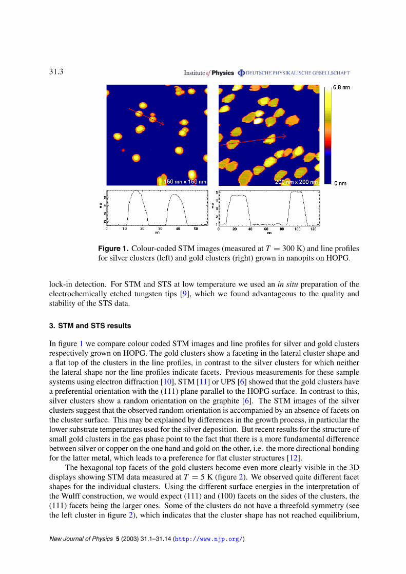
Figure 1. Colour-coded STM images (measured at T = 300 K) and line profilesfor silver clusters (left) and gold clusters (right) grown in nanopits on HOPG.
lock-in detection. For STM and STS at low temperature we used an in situ preparation of theelectrochemically etched tungsten tips [9], which we found advantageous to the quality andstability of the STS data.
3. STM and STS results
In figure 1 we compare colour coded STM images and line profiles for silver and gold clustersrespectively grown on HOPG. The gold clusters show a faceting in the lateral cluster shape anda flat top of the clusters in the line profiles, in contrast to the silver clusters for which neitherthe lateral shape nor the line profiles indicate facets. Previous measurements for these samplesystems using electron diffraction [10], STM [11] or UPS [6] showed that the gold clusters havea preferential orientation with the (111) plane parallel to the HOPG surface. In contrast to this,silver clusters show a random orientation on the graphite [6]. The STM images of the silverclusters suggest that the observed random orientation is accompanied by an absence of facets onthe cluster surface. This may be explained by differences in the growth process, in particular thelower substrate temperatures used for the silver deposition. But recent results for the structure ofsmall gold clusters in the gas phase point to the fact that there is a more fundamental differencebetween silver or copper on the one hand and gold on the other, i.e. the more directional bondingfor the latter metal, which leads to a preference for flat cluster structures [12].
The hexagonal top facets of the gold clusters become even more clearly visible in the 3Ddisplays showing STM data measured at T = 5 K (figure 2). We observed quite different facetshapes for the individual clusters. Using the different surface energies in the interpretation ofthe Wulff construction, we would expect (111) and (100) facets on the sides of the clusters, the(111) facets being the larger ones. Some of the clusters do not have a threefold symmetry (seethe left cluster in figure 2), which indicates that the cluster shape has not reached equilibrium,
New Journal of Physics 5 (2003) 31.1–31.14 (http://www.njp.org/)

31.4
Figure 2. 3D displays of STM images (measured at T = 5 K) for three individualgold clusters grown in nanopits on HOPG. The image size and the cluster heighth is given for each image.
but is still influenced by the growth process, e.g. the coalescence of several smaller clusters,grown at the pit edge, to one larger cluster.
We measured nearly identical data for the tunnelling current I with a variation of thetunnelling gap, i.e. I (z) on top of the clusters and on the HOPG respectively (not shown), whichindicates that the height measured with the STM will be close to the geometric height of theclusters. In contrast to the inflation of the total lateral cluster size [5] the imaging of the flat (111)facet is not hindered by the convolution with the tip shape. We assume that the cluster side facetsare formed by (111) and (100) surfaces making an angle of 70.5 and 54.7 respectively with theHOPG surface [13]. With this the cluster volume of the individual clusters can be calculated ingood approximation using a truncated cone with an angle of 60 to the HOPG surface and thefacet as the top surface.
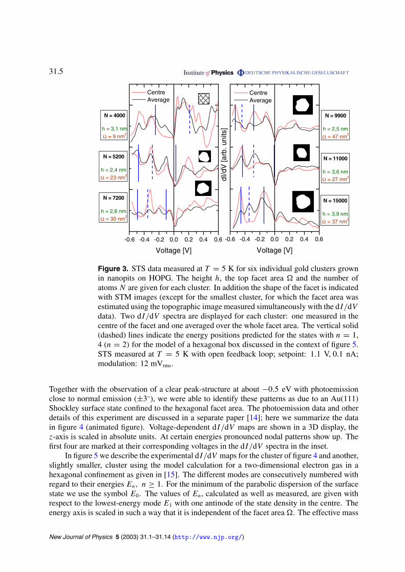
In figure 3 we present dI/dV spectra measured for six individual gold clusters, togetherwith the shape and the size of the facets as well as the cluster heights h. The resulting numberof atoms N was calculated as described above. Two dI/dV spectra are given for each cluster:one measured for a small area at the centre of the facet and one averaged over the whole facetarea. With the spectra measured in the facet-centre we select only electron states with a certainsymmetry (cf the discussion of figure 5 below). The spectra averaged over the whole facet area,less well defined, include all states. Hence, the comparison of the two curves allows a roughestimation of the spatial distribution. The facet area varies for the five larger clusters within therange of a factor of two; the same applies to the height of the six clusters. The volume of thelargest cluster is about four times larger than that of the smallest one. The cluster spectra arestrongly structured with peaks of several 10 meV width, measured with a sinusoidal modulationvoltage of 12 meVrms, which will not lead to a significant additional broadening. In contrastthe spectra taken on the HOPG surface have a smooth V-shape (see [8]). We discuss the clusterspectra in the following sections in view of confined surface and volume states.
4. Confined surface states
First, we focus on the largest cluster with N = 1.5 × 10⁴ atoms in figure 3. For this clusterwe observed a pronounced nodal pattern in the dI/dV maps measured on the top (111) facet.
New Journal of Physics 5 (2003) 31.1–31.14 (http://www.njp.org/)
31.5
-0.6 -0.4 -0.2 0.0 0.2 0.4 0.6 -0.6 -0.4 -0.2 0.0 0.2 0.4 0.6
Centre Average
Centre Average
N = 5200
h = 2,4 nmΩ = 23 nm2
N = 4000
h = 3,1 nmΩ = 9 nm2
N = 15000
h = 3,9 nmΩ = 37 nm2
N = 11000
h = 3,6 nmΩ = 27 nm2
N = 7200
h = 2,6 nmΩ = 30 nm2
dI/d
V [a
rb. u
nits
]
Voltage [V]
N = 9900
h = 2,5 nmΩ = 47 nm2
Voltage [V]
Figure 3. STS data measured at T = 5 K for six individual gold clusters grownin nanopits on HOPG. The height h, the top facet area and the number ofatoms N are given for each cluster. In addition the shape of the facet is indicatedwith STM images (except for the smallest cluster, for which the facet area wasestimated using the topographic image measured simultaneously with the dI/dV
data). Two dI/dV spectra are displayed for each cluster: one measured in thecentre of the facet and one averaged over the whole facet area. The vertical solid(dashed) lines indicate the energy positions predicted for the states with n = 1,4 (n = 2) for the model of a hexagonal box discussed in the context of figure 5.STS measured at T = 5 K with open feedback loop; setpoint: 1.1 V, 0.1 nA;modulation: 12 mVrms.
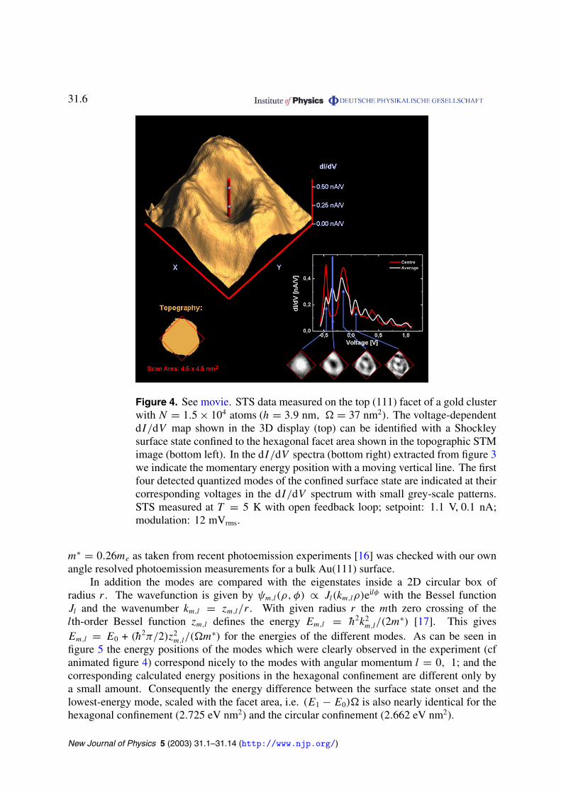
Together with the observation of a clear peak-structure at about −0.5 eV with photoemissionclose to normal emission (±3), we were able to identify these patterns as due to an Au(111)Shockley surface state confined to the hexagonal facet area. The photoemission data and otherdetails of this experiment are discussed in a separate paper [14]; here we summarize the datain figure 4 (animated figure). Voltage-dependent dI/dV maps are shown in a 3D display, thez-axis is scaled in absolute units. At certain energies pronounced nodal patterns show up. Thefirst four are marked at their corresponding voltages in the dI/dV spectra in the inset.
In figure 5 we describe the experimental dI/dV maps for the cluster of figure 4 and another,slightly smaller, cluster using the model calculation for a two-dimensional electron gas in ahexagonal confinement as given in [15]. The different modes are consecutively numbered withregard to their energies En, n ≥ 1. For the minimum of the parabolic dispersion of the surfacestate we use the symbol E0. The values of En, calculated as well as measured, are given withrespect to the lowest-energy mode E1 with one antinode of the state density in the centre. Theenergy axis is scaled in such a way that it is independent of the facet area . The effective mass
New Journal of Physics 5 (2003) 31.1–31.14 (http://www.njp.org/)
31.6
Figure 4. See movie. STS data measured on the top (111) facet of a gold clusterwith N = 1.5 × 10⁴ atoms (h = 3.9 nm, = 37 nm2). The voltage-dependentdI/dV map shown in the 3D display (top) can be identified with a Shockleysurface state confined to the hexagonal facet area shown in the topographic STMimage (bottom left). In the dI/dV spectra (bottom right) extracted from figure 3we indicate the momentary energy position with a moving vertical line. The firstfour detected quantized modes of the confined surface state are indicated at theircorresponding voltages in the dI/dV spectrum with small grey-scale patterns.STS measured at T = 5 K with open feedback loop; setpoint: 1.1 V, 0.1 nA;modulation: 12 mVrms.
m∗ = 0.26me as taken from recent photoemission experiments [16] was checked with our ownangle resolved photoemission measurements for a bulk Au(111) surface.
In addition the modes are compared with the eigenstates inside a 2D circular box ofradius r . The wavefunction is given by ψm,l(ρ, φ) ∝ Jl(km,lρ)eilφ with the Bessel functionJl and the wavenumber km,l = zm,l/r . With given radius r the mth zero crossing of thelth-order Bessel function zm,l defines the energy Em,l = h2k2
m,l/(2m∗) [17]. This givesEm,l = E0 + (h2π/2)z2
m,l/(m∗) for the energies of the different modes. As can be seen infigure 5 the energy positions of the modes which were clearly observed in the experiment (cfanimated figure 4) correspond nicely to the modes with angular momentum l = 0, 1; and thecorresponding calculated energy positions in the hexagonal confinement are different only bya small amount. Consequently the energy difference between the surface state onset and thelowest-energy mode, scaled with the facet area, i.e. (E1 − E0) is also nearly identical for thehexagonal confinement (2.725 eV nm2) and the circular confinement (2.662 eV nm2).
New Journal of Physics 5 (2003) 31.1–31.14 (http://www.njp.org/)

31.7
11
10
n density h = 3.9 nmΩ = 37 nm2
N = 15000
hexagon experiment
h = 2.5 nmΩ = 47 nm2
N = 9900
(E-E
1)⋅Ω
[eV
nm2 ]
0
10
20
30
40
50
13
1
2
34
56
7
8
9
12
circle
(1,0)
(1,1)
(2,0)
(2,1)
(3,0)
(3,1)
(m,l)
Figure 5. Left column (‘hexagon’): energies for the different quantized modes(numbered with n = 1 . . . 13) of a two-dimensional electron gas confined toa hexagonal box calculated using the theory from [15]. An effective massm∗ = 0.26me was used for the dispersion E(k‖). For those modes which areclearly observed in the experiment, we display in addition the correspondingcalculated state densities as given in [15]. Middle column (‘experiment’):measured energies and dI/dV maps for two clusters with different facet areas ,heights h and the resulting number of atoms N . Right column (‘circle’): energiesfor the modes with l = 0 and 1 of a two-dimensional electron gas confined to acircular box [17]. The vertical axis is scaled in a way, that it is independent fromthe hexagonal (respectively circular) area .
In order to fit the absolute energetic position of the first centre antinode mode E1, theminimum of the surface state parabolic dispersion has to be set to E0 = −528 and −588 meVfor the clusters with h = 3.9 and 2.5 nm respectively, i.e. shifted to lower energies comparedwith the onset of the surface state band on a macroscopic gold surface (−487 meV) [16]. Thiscan be related to the shift of the surface state to lower energy for thin metal films due to theinteraction with the substrate within the decay length of the surface state [18] or with possibleshifts due to film strain [19]. We use the two fixed points for E0(h) given above together withthe limiting value E0(∞) = −487 meV to set up a parametrization of E0(h) as used in [18].This results in the formula E0(h) = −487 meV−491 meV ·exp(−h/1.581 nm). Together withthe model for the confinement of the two-dimensional electron gas to a hexagonal box from [15]
New Journal of Physics 5 (2003) 31.1–31.14 (http://www.njp.org/)

31.8
-0.6 -0.4 -0.2 0.0 0.2 0.4 0.6
CentreAverage
dI/d
V[a
rb.u
nits
]
Voltage [V]
-0.49 V -0.31 V -0.10 V +0.21 V +0.35 V +0.43 V
Figure 6. dI/dV spectra and dI/dV maps (3×3 nm2) measured on the top (111)facet of a gold cluster with N = 5.2 × 10³ atoms (h = 2.4 nm, = 23 nm2).The centre of the facet corresponds to the bright white spot in the dI/dV map for+0.21 V. STS measured at T = 5 K with open feedback loop; setpoint: 1.1 V,0.1 nA; modulation: 12 mVrms.
we can now calculate predicted energy positions for all the different clusters. The cluster heightdetermines the surface state onset, while the scaling for the peak positions is given by the facetarea. We have indicated the energy positions predicted for the states with n = 1, 4 (and n = 2)
in figure 3 with solid (and dashed) lines respectively.For the three largest clusters almost all of the modes can be identified in the dI/dV spectra.
The mode at −441 meV for the N = 9.9 × 10³ cluster is visible as a shoulder; however, it canbe clearly identified in the corresponding dI/dV maps (cf figure 5). The mode at −9 meV forthe N = 1.1 × 10⁴ cluster is suppressed by the dip at the Fermi energy, which will be discussedin section 5.
The agreement for the three smallest clusters is much worse. For the clusters withN = 7.2 × 10³ and 5.2 × 10³ one can observe a peak near the energy predicted for the E2
mode, but the peaks for E1 are not visible, and no agreement at all is obtained for the clusterwith N = 4.0 × 10³.
In figure 6 we show dI/dV spectra and maps for the cluster with N = 5.2×10³ atoms. Analternation between a maximum and a minimum in the centre of the facet area is also present inthis case, and the nodal pattern is still visible but much less pronounced than in the case of thelarger clusters discussed in figures 4 and 5. This corresponds to the smaller differences betweenthe dI/dV spectra measured in the centre or taken as the average over the whole facet area. Thedescription using a confined Shockley surface state does not fit to this case, as becomes obviousfor the peak at −0.31 eV which is predicted to be a mode with n = 2, i.e. with a node in thecentre of the dI/dV map, in contrast to the measured antinode in the centre. We will discuss analternative assignment for the modes of the smaller clusters in the next section.
New Journal of Physics 5 (2003) 31.1–31.14 (http://www.njp.org/)
31.9
-1.0 -0.5 0.0 0.5 1.0
dI/d
V[a
rb.u
nits
]
Voltage [V]
(a)
(b)
-1.0 -0.5 0.0 0.5 1.0
dI/d
V[a
rb.u
nits
]
Voltage [V]
(a)
(b)
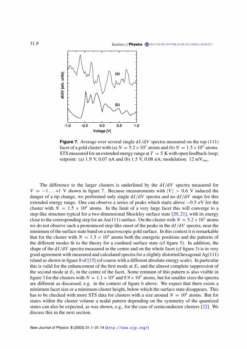
Figure 7. Average over several single dI/dV spectra measured on the top (111)facet of a gold cluster with (a) N = 5.2×10³ atoms and (b) N = 1.5×10⁴ atoms.STS measured for an extended energy range at T = 5 K with open feedback-loop;setpoint: (a) 1.9 V, 0.07 nA and (b) 1.5 V, 0.08 nA; modulation: 12 mVrms.
The difference to the larger clusters is underlined by the dI/dV spectra measured forV = −1 . . . +1 V shown in figure 7. Because measurements with |V | > 0.6 V induced thedanger of a tip change, we performed only single dI/dV spectra and no dI/dV maps for thisextended energy range. One can observe a series of peaks which starts above −0.5 eV for thecluster with N = 1.5 × 10⁴ atoms. In the limit of a very large facet this will converge to astep-like structure typical for a two-dimensional Shockley surface state [20, 21], with its energyclose to the corresponding step for an Au(111) surface. On the cluster with N = 5.2×10³ atomswe do not observe such a pronounced step-like onset of the peaks in the dI/dV spectra, near theminimum of the surface state band on a macroscopic gold surface. In this context it is remarkablethat for the cluster with N = 1.5 × 10⁴ atoms both the energetic positions and the patterns ofthe different modes fit to the theory for a confined surface state (cf figure 5). In addition, theshape of the dI/dV spectra measured in the centre and on the whole facet (cf figure 3) is in verygood agreement with measured and calculated spectra for a slightly distorted hexagonal Ag(111)island as shown in figure 8 of [15] (of course with a different absolute energy scale). In particularthis is valid for the enhancement of the first mode at E1 and the almost complete suppression ofthe second mode at E2 in the centre of the facet. Some remnant of this pattern is also visible infigure 3 for the clusters with N = 1.1×10⁴ and 9.9×10³ atoms, but for smaller sizes the spectraare different as discussed, e.g. in the context of figure 6 above. We expect that there exists aminimum facet size or a minimum cluster height, below which the surface state disappears. Thishas to be checked with more STS data for clusters with a size around N = 104 atoms. But forstates within the cluster volume a nodal pattern depending on the symmetry of the quantizedstates can also be expected, as was shown, e.g., for the case of semiconductor clusters [22]. Wediscuss this in the next section.
New Journal of Physics 5 (2003) 31.1–31.14 (http://www.njp.org/)

31.10
5. Electron confinement in the cluster volume
For thin metal films the confinement of the conduction electrons perpendicular to the filmthickness leads to ‘quantum well states’, which basically correspond to the one-dimensional‘particle-in-a-box’ problem. The resulting discrete energy levels were studied in the pastmainly with photoelectron spectroscopy [23, 24] but recently also STS has been used for localmeasurements [25]. Experiments for a freestanding metal film with nanoscopic thickness wereperformed for small gas bubbles a few crystal monolayers below the surface [26], but mostsamples consist of a thin metal film grown on a substrate. In the latter case the barrier for theelectron transmission into the substrate occurs, e.g. for energies within a bandgap of the substratematerial, or due to different symmetries of the electron states in the film and in the substrate.
But for the Au clusters the application of such quantum well states is not straightforward.In spite of the flat (111) facets on top of the gold clusters a simple square-well potential of awidth corresponding to the cluster height, similar to [27], does not give a description of the peakpositions. Using this model the valence band energy level spacing close to the Fermi energy isE ≈ πh2kF/(m∗dz). With kF ≈ 1.2 × 10¹⁰ m−1, m∗ ≈ 1 and dz = 3 nm corresponding tothe mean cluster heights, this results in E ≈ 1 eV. Indeed this is the experimentally observedvalue for quantum well states, e.g. in an Ag(100) film of about this thickness [28] with m∗ ≈ 0.7for the direction perpendicular to the film surface. Within this model the experimentally observedE ≈ 0.2 eV for the gold clusters requires significantly altered material properties such as, e.g.,an increased effective mass m∗ 1. But this contradicts the existence of a Shockley surfacestate, as was observed on the facets of the largest clusters (see section 4), which indicates anelectronic structure which is already very close to the bulk properties. The interaction of thevalence band electrons with the lattice of the ionic cores can have a significant effect on the energyquantization for quantum well states in thin metal films [24]. In general, they cannot be describedby a simple free electron gas, but band structure effects have to be considered. Applying the bulkband structure to an Au(111) film, quantum well states in the occupied region are expected onlyfor energies below the valence band maximum at −1 eV, due to the gap in the surface-projectedvolume band structure [29, 30]. This region is not covered by the spectra in figure 3, for technicalreasons (cf the discussion of figure 7). An energy quantization in the valence band below the gapin the (111) direction was found for Ag(111) films on HOPG [31]. In addition one observes theexistence of surface states on these (111) films [18, 19], with a shifted energy position comparedwith the bulk surface due to the interaction with the substrate (cf section 4). This shows that themain features of the band structure for the direction perpendicular to the film surface remain,though the thickness of only a few atomic layers would suggest an ill-defined k⊥. The sameobservation is also made for other properties of thin metal films such as, e.g., the photon energydependence in the normal emission photoelectron signal [23]. For the case of faceted metalclusters this corresponds to the previously discussed presence of detailed properties connectedwith the bulk band structure, already for clusters with a diameter of a few nanometres.
The disagreement between the calculated modes and the measured spectra for the threesmaller clusters in figure 3 suggests that the surface state disappears below a critical cluster sizeof about 104 atoms. Qualitatively the series of patterns in the dI/dV maps are still visible,but the energies of the modes do not fit to the model applied for the confined surface state insection 4 (cf figure 6). For the cluster with N = 5.2 × 10³ atoms we can get considerablybetter agreement if we assume a significantly increased facet area of ′ = 41 nm2 instead of themeasured value = 23 nm2, and if we shift the onset of the surface state to E′
0 = −660 meV.
New Journal of Physics 5 (2003) 31.1–31.14 (http://www.njp.org/)

31.11
With these modified parameters we get the energies −592, −490, −310, −100 and 179 meV forthe modes with n = 1, 2, 4, 7 and 10, respectively (cf experimental data in figures 6 and 7). Asimilar identification of the peaks in the dI/dV spectra together with the corresponding dI/dV
maps can be obtained for the cluster with N = 7.2 × 10³ atoms assuming ′ = 51 nm2 andE′
0 = −605 meV. The model of section 4 predicts a similar E0 for clusters with N = 5.2 × 103,7.2 × 103 and 9.9 × 10³, because of their similar height. In contrast, the values of E′
0 for thetwo clusters discussed above are significantly smaller than for the cluster with N = 9.9 × 10³
(E0 = −588 meV).Up to now the modified parameters E′
0 and ′ for the smaller clusters are purely heuristic.The values for ′ are not unreasonable, since they are in between the area of the top and thebottom facet of the clusters, but we remark that we would also get the same result by changingthe effective electron mass, which would shift m∗ closer to me, the value for a free electron gas.On the whole, the modifications can be taken as an indication that the spectra for the smallerclusters show the transition from peaks given by confined surface states to features induced bythe modification of electronic volume properties with decreasing cluster dimensions. For verysmall clusters the connection to different bulk phenomena will get less well defined, and theelectronic structure is better described by a three-dimensional electron confinement, e.g. withthe well-known jellium model [1], in which the effect of the ionic cores can be included asperturbation [3].
Finally we would like to mention the minimum which is located for all clusters in figure 3at V = 0, i.e. at the Fermi energy. It can be excluded that this feature is caused by an artefactwithin the lock-in detection because we see it identically, only with a smaller signal-to-noiseratio, in the I (V ) curves after numerical differentiation. One would not expect the Fermi energyto be special, neither for surface nor for volume states, if the dI/dV spectra simply represent thedensity for the confined and quantized states. Therefore this minimum indicates that the dI/dV
spectra cannot be interpreted solely as given by the local density of states. Effects like the chargetransport in the tip/cluster/surface system [32], perhaps in combination with the vanishing densityof states at the Fermi energy for the HOPG substrate, have to be considered as well.
6. Band structure effects in the energy quantization
In figure 8 we present a schematic illustration for the discussed ‘bulk limit’ in the descriptionof large faceted metal clusters, focusing on a (111) facet of a noble metal cluster. Two crosssections of the bulk band structure are shown: on the left-hand side E(k⊥) for the directionperpendicular to the surface, with the parabolic maximum or minimum for the valence bandbelow or above the gap in the (111) direction respectively; and on the right-hand side the curveE(k||) for the Shockley surface state within the gap in the shaded projected volume band structure.In both directions a confinement will lead to an energy quantization. For a laterally extendedthin metal film, quantum well states will occur below and above the gap in the (111) direction.The confinement of the Shockley surface state to a nanoscopic facet area will lead to quantizedmodes, too. Measuring the electronic structure of a large, faceted cluster one may observe acombination of both, as indicated in the energy spectrum in the middle. In addition quantizedvolume states can exist inside the bandgap, if an electron confinement occurs for other than thehigh-symmetry (111) direction [26].
For the actual experimental result the choice of the spectroscopic technique will be crucial.The density of states at the Fermi level is given by m∗/(πh2) for the surface state (without
New Journal of Physics 5 (2003) 31.1–31.14 (http://www.njp.org/)

31.12
k||
EE
k⊥⊥⊥⊥(k|| = 0) D(E)
EF
E
bandgap
2D confined surface states1D confined quantum wellstates
k||
EE
k⊥⊥⊥⊥(k|| = 0) D(E)
EF
E
bandgap
2D confined surface states1D confined quantum wellstates
Figure 8. Schematic illustration for the ‘bulk limit’ in the description of large,faceted noble metal clusters. Left: E(k⊥) for the direction perpendicular to a(111) facet. Right: E(k||) with the Shockley surface state on a (111) facet. Centre:energy spectrum D(E) for a large, faceted noble metal cluster assumed to be acombination of modes given by perpendicular and lateral electron confinement.
confinement) and by (2me)3/2(−EV )1/2V/(2π2h3) for the volume states (for a free electron gas)
with EV = −5.5 eV for the valence band minimum of gold with respect to the Fermi energy.Inserting the facet area and the volume V for the cluster presented in figure 4, this gives adensity of states which is about 100 times larger for the volume states than for the surface states.Therefore it will be difficult to detect the surface state, e.g. for free clusters. Nevertheless, forthe gold clusters on graphite here the surface state could be observed because angular selectivityin the photoemission experiment and the surface sensitivity of STS were employed. The relativecontribution of the confined surface state is larger for certain energies due to the emergenceof discrete modes, and it will be important to include it in the discussion, in particular forprocesses which are localized at the cluster surface, such as adsorption processes [33] or growthphenomena [34]–[37] for example.
The existence of Shockley surface states is expected to be restricted to large facets on thecluster surface. Up to now we have measured STS spectra for clusters without facets only forcluster sizes below about N = 6×10² atoms [8]. One reason is, that the STS measurement oftenleads to a displacement of larger clusters, probably due to lateral force components between thecluster and the STM tip. This in particular is the case if one cannot profit from the extremelystable tunnelling conditions on a flat top facet. Extending the STS measurements to larger clusterswithout facets will be of interest to test how the electronic structure depends on the cluster shape.
7. Conclusion
In the limit of large, faceted metal clusters the interaction of the free electron gas with theionic core lattice results in additional quantization phenomena which are well known in the areaof surface and thin-film physics. We have discussed this topic using experimental results forlarge noble metal clusters grown on HOPG. For faceted gold clusters we observed one explicitexample for this kind of effect with the emergence of a Shockley surface state for clusters witha size of 104 atoms. The lateral two-dimensional confinement of the surface state within the(111) facet area leads to quantized states, which may be important for processes on the cluster
New Journal of Physics 5 (2003) 31.1–31.14 (http://www.njp.org/)

31.13
surface due to the resulting large density of states at certain positions close to the Fermi energy.For the three-dimensional electron confinement, in particular also perpendicular to the surface,the wealth of experimental and theoretical work which exists for quantum well states in metalfilms on surfaces may lead to a deeper understanding for the case of large metal clusters as well.The interconnections between this kind of ‘bulk limit’, using the bulk volume and surface bandstructure as a starting point for the description of large clusters, and the models successfully usedfor the description of small metal clusters, e.g. the jellium model, are still to be explored.
Acknowledgment
The authors would like to acknowledge support by the Deutsche Forschungsgemeinschaft (Ho-1597/3-3).
References
[1] Ekardt W 1984 Phys. Rev. B 29 1558[2] deHeer W A 1993 Rev. Mod. Phys. 65 611[3] Schone W-D, Ekardt W and Pacheco J M 1994 Phys. Rev. B 50 11079[4] Hovel H, Becker T, Funnemann D, Grimm B, Quitman C and Reihl B 1998 J. Electron Spectrosc. Relat.
Phenom. 88–91 1015[5] Hovel H, Becker Th, Bettac A, Reihl B, Tschudy M and Williams E J 1997 J. Appl. Phys. 81 154[6] Hovel H 2001 Appl. Phys. A 72 295[7] Hovel H, Grimm B, Pollmann M and Reihl B 1998 Phys. Rev. Lett. 81 4608[8] Hovel H, Grimm B, Bodecker M, Fieger K and Reihl B 2000 Surf. Sci. 463 L603[9] Albrektsen O, Salemink H W M, Mørch K A and Tholen A R 1994 J. Vac. Sci. Technol. B 12 3187
[10] Hovel H, Becker Th, Bettac A, Reihl B, Tschudy M and Williams E J 1997 Appl. Surf. Sci. 115 124[11] Zhu Y J, Schnieders A, Alexander J D and Beebe T P 2002 Langmuir 18 5728[12] Hakkinen H, Moseler M and Landman U 2002 Phys. Rev. Lett. 89 033401[13] Hansen K H, Worren T, Stempel S, Lægsgaard E, Baumer M, Freund H-J, Besenbacher F and Stensgaard I
1999 Phys. Rev. Lett. 83 4120[14] Barke I and Hovel H 2003 Phys. Rev. Lett. at press[15] Li J, Schneider W-D, Crampin S and Berndt R 1999 Surf. Sci. 422 95[16] Reinert F, Nicolay G, Schmidt S, Ehm D and Hufner S 2001 Phys. Rev. B 63 115415[17] Crommie M F, Lutz C P and Eigler D M 1993 Science 262 218[18] Patthey F and Schneider W-D 1995 Surf. Sci. 334 L715[19] Neuhold G and Horn K 1997 Phys. Rev. Lett. 78 1327[20] Hasegawa Y and Avouris Ph 1993 Phys. Rev. Lett. 71 1071[21] Crommie M F, Lutz C P and Eigler D M 1993 Nature 363 524[22] Millo O, Katz D, Cao Y W and Banin U 2001Phys. Rev. Lett. 86 5751[23] Milun M, Pervan P and Woodruff D P 2002 Rep. Prog. Phys. 65 99[24] Chiang T C 2000 Surf. Sci. Rep. 39 181[25] Chen D M 2000 J. Electron Spectrosc. Relat. Phenom. 109 85 and references therein[26] Schmid M, Hebenstreit W, Varga P and Crampin S 1996 Phys. Rev. Lett. 76 2298
Schmid M, Crampin S and Varga P 2000 J. Electron Spectrosc. Relat. Phenom. 109 71[27] Bettac A, Koller L, Rank V and Meiwes-Broer K-H 1998 Surf. Sci. 402–404 475[28] Paggel J J, Miller T and Chiang T-C 1999 Science 283 1709[29] Knoppe H and Bauer E 1993 Phys. Rev. B 48 5621[30] Shikin A M, Rader O, Prudnikova G V, Adamchuk V K and Gudat W 2002 Phys. Rev. B 65 075403
New Journal of Physics 5 (2003) 31.1–31.14 (http://www.njp.org/)

31.14
[31] Patthey F and Schneider W-D 1994 Phys. Rev. B 50 17560[32] Hanna A E and Tinkham M 1991 Phys. Rev. B 44 5919[33] Memmel N 1998 Surf. Sci. Rep. 32 91[34] Morgenstern K, Rosenfeld G, Comsa G, Lægsgaard E and Besenbacher F 2000 Phys. Rev. Lett. 85 468[35] Giesen M and Ibach H 2000 Phys. Rev. Lett. 85 469[36] Knorr N, Brune H, Epple M, Hirstein A, Schneider M A and Kern K 2002 Phys. Rev. B 65 115420[37] Repp J, Moresco F, Meyer G and Rieder K-H 2000 Phys. Rev. Lett. 85 2981
New Journal of Physics 5 (2003) 31.1–31.14 (http://www.njp.org/)