Status and outlook of the Medipix3 TSV project Timo Tick – Medipix3 Open meeting 25.1.2012.

Large-area Medipix3 project
Sabine SengelmannDetector Group DESY
Medipix meeting, September 23, 2010

Sabine Sengelmann | Large area Medipix 3 | September 23, 2010 | Page 2
Large-area Medipix3 project
Requirements:
• Large area
• High frame rate
• experiments up to 100 keV

Sabine Sengelmann | Large area Medipix 3 | September 23, 2010 | Page 3
Large-area Medipix3 project
Assembly
Sabine Sengelmann | Large area Medipix 3 | September 23, 2010 | Page 4
Germanium detector Large-area Medipix3 project
Module ceramic
Heat spreader
Voltage regulator board
2 high-Z sensors
Each 42 mm * 28 mm
3*2 Medipix 3 chips under each sensor
Cooling block1 Silicon sensors
84 mm * 28 mmor

Sabine Sengelmann | Large area Medipix 3 | September 23, 2010 | Page 5
Readout chip
Sensor
Readout chip
Module ceramicHeat spreader
Sensor
Medipix Medipix
Medipix Medipix
Medipix Medipix
Medipix Medipix
Medipix
Medipix
Medipix
Medipix
Wire bonds
28mm
85mm
Top view
Side view
Large-area Medipix3 project

Sabine Sengelmann | Large area Medipix 3 | September 23, 2010 | Page 6
3 modules gives ~9*9cm2 (2.3 Mpixel)
12 modules gives 18*18cm2 (9.4Mpixel)
essential:
Minimal dead area between modules
Large area
Sabine Sengelmann | Large area Medipix 3 | September 23, 2010 | Page 7
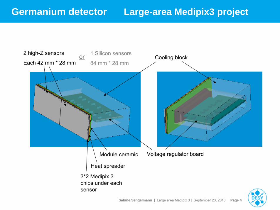
PCB for voltage regulators
10 gigabit Ethernet
Sensor assembly on module ceramic
FPGA
Connector through chamber or seal
Intelligent board
sens
orR
eado
ut c
hip PC
BH
eat s
prea
der
Cooling block
Cooling block
Large-area Medipix3 project
Readout:
First version: FITPIX or RUIN readout
Final version: Modify a XFEL board (designed for XFEL)
Sabine Sengelmann | Large area Medipix 3 | September 23, 2010 | Page 8
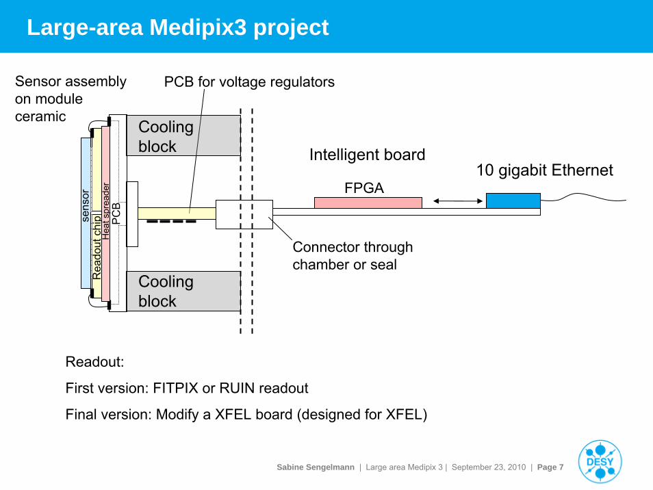
Connections required
> 12 chips, each using 8 DataOut lines to achieve 2000Hz max readout speed
> Parallel O Serial I scheme, dividing chips into 2 sets of 6
26 input + 120 output LVDS pairs
> Power3 voltage levels
Around 11A total current
Voltage regulators on second board
240 pin version (no picture of the 500 pin version available)
500 pin version

Sabine Sengelmann | Large area Medipix 3 | September 23, 2010 | Page 9
High-Z materials
0%
20%
40%
60%
80%
100%
120%
0 20 40 60 80 100
Prop
ortio
n ab
sorb
ed /
inte
ract
ing
X-ray energy (keV)
X-ray absorption / interaction
Silicon (500um)Ge / GaAs (500um)CdTe (500um)
> Many Petra-III (DESY synchrotron) experiments up to 100 keV x-rayReplace silicon with another semiconductor
> Germanium: Germanium (Canberra),
Still tests: How sensitive are diodes to high temperatures
Indium bump bonding (IZM) Relatively cold bonding ( <100°C)

Sabine Sengelmann | Large area Medipix 3 | September 23, 2010 | Page 10
> Germanium detector needs -50°CAvoid large temperature differences (leakage doubles every 9°C)
> Each chip up to 1.5W → design for 18W power
> Normal heat-spreader and cooling block at one side is not sufficientEstimate ΔT≥15°C, even with thermal contacts at each end
> Thermal vias through board
> Thermal coupling to each chipHeat spreader reduces heat gradient and helps match CTE
Estimate ΔT=2°C across sensor (plus 5°C through vias)
Germanium Mechanics and cooling

Sabine Sengelmann | Large area Medipix 3 | September 23, 2010 | Page 11
Ceramic PCB
Thermal expansion:
Silicon: ~ 2.5 ppm/°C
Germanium: ~ 5.9 ppm/°C
• difference of 3.4ppm/C
• operate at -50°C – 75°C
• 7um displacement along diagonal
diagonal of 51mmtemp difference 100K
~ 2 um (Ceramic)
mismatch of(Germ. → PCB)30.1um
38.3um
76.5um
28.1um
Germanium: ~ 5.9 ppm/°C
Heat spreader CuG: ~ 7-8 ppm/°C
FR4 PCB: ~ 12 – 18 ppm/°C
Ceramic PCB: ~ 5.5 ppm/°C
mismatch of(Silicon → Germ.)
~ 3.5um
from centre to corner
~ 46.4 um (FR4)
from centre to corner
Result:

Sabine Sengelmann | Large area Medipix 3 | September 23, 2010 | Page 12
Design issues
> Cooling frame occupies space on the back underneath each PCB
> Space available for connectors reduced
> Thermal vias make routing more difficult
Thermal vias
Mechanics and cooling

Sabine Sengelmann | Large area Medipix 3 | September 23, 2010 | Page 13
PCB
Heat spreaderReadout chip
Sensor
~ 700 μm~ 500 μm
PCB design → Minimise dead area between modules
Challenging:
> Wire bonding
> Routing
> Find a manufacturer
Wire bonding
Sabine Sengelmann | Large area Medipix 3 | September 23, 2010 | Page 14
Status of the project

Sabine Sengelmann | Large area Medipix 3 | September 23, 2010 | Page 15
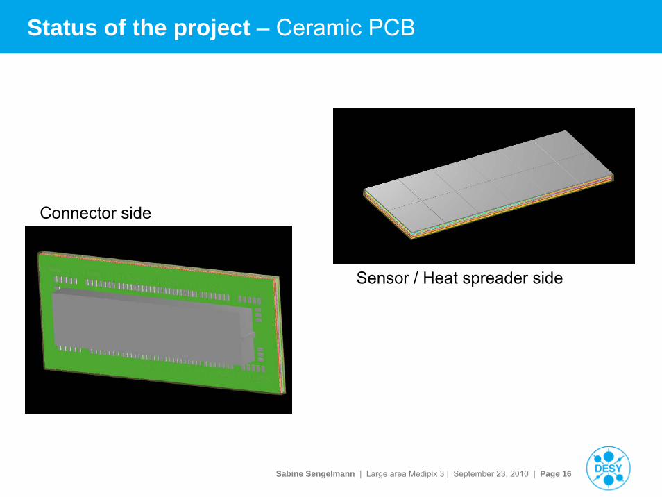
Status of the project – Ceramic PCB
Production of the ceramic PCB will start next week
few companies are using LTCC (Low temperature co-fired ceramic) multi-layer technology → clearances of some still to big
Sabine Sengelmann | Large area Medipix 3 | September 23, 2010 | Page 16
Status of the project – Ceramic PCB
Connector side
Sensor / Heat spreader side
Sabine Sengelmann | Large area Medipix 3 | September 23, 2010 | Page 17
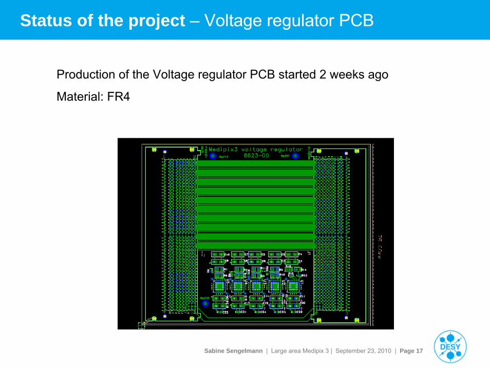
Status of the project – Voltage regulator PCB
Production of the Voltage regulator PCB started 2 weeks ago
Material: FR4
Sabine Sengelmann | Large area Medipix 3 | September 23, 2010 | Page 18
Outlook
> End of this year: Board tests
> Beginning of next year: Mounting full Si-sensors
> Next year: Fast readout
Large-area Medipix3 project

Sabine Sengelmann | Large area Medipix 3 | September 23, 2010 | Page 19
Large-area Medipix3 project
Thanks for listening