Lab 11 Graphene - MIT OpenCourseWare · Pappalardo II Micro/Nano Instructors: Teaching ... the...
25
Graphene 0 2.674 Lab 11 Spring 2016 Pappalardo II Micro/Nano Instructors: Teaching Laboratory Prof. Jeehwan Kim Prof. Sang-Gook Kim Dr. Benita Comeau Mr. Andrew Jones
Transcript of Lab 11 Graphene - MIT OpenCourseWare · Pappalardo II Micro/Nano Instructors: Teaching ... the...

Graphene
0
2.674 Lab 11
Spring 2016
Pappalardo II Micro/Nano Instructors: Teaching Laboratory Prof. Jeehwan Kim
Prof. Sang-Gook Kim Dr. Benita Comeau Mr. Andrew Jones
Lab #11: Graphene
1
I. Introduction
1. Graphene
As we learnt from Lab #7, graphene is a basic building block of carbon-based nanomaterials such as CNT and fullerene. It can be three-dimensionally piled to form graphite, one-dimensionally rolled to form nanotubes, and zero-dimensionally balled up to form fullerenes. Graphene is a single-atom-thick, two-dimensional sheet of sp2-bonded carbon [1]. Graphene has a periodic honey-comb lattice as shown in Figure 1. Since there are three laterally shared bondings in carbon atoms, a remaining vertical bond forms π-conjugation which is the source of exceptional electrical, thermal, and mechanical properties (see Figure 2). These exceptional properties can be maintained by keeping its two-dimensional form. Among all existing materials, electron mobility is fastest in graphene which is 10-100 times faster than that in other materials as shown in Table 1. Therefore, graphene is emerging as a candidate for a next generation high speed transistor. Thermal conductivity in graphene is 2 times greater than that in diamond and 10 times higher than that in copper. Young’s modulus of graphene is 5 times higher than that of steel but extremely flexible. In 2004, Andre Geim and Konstantin Novoselov at the University of Manchester first demonstrated successful isolation of single-layer of graphite, which is graphene [2]. Thanks to this groundbreaking work, they won the Nobel Prize in Physics in 2010 “for groundbreaking experiments regarding the two-dimensional material graphene.” This ignited substantial interest in graphene and extensive research has been performed by many scientists in the world since then. The global market for graphene is reported to reach $150 million by 2020 for various application spaces (https://www.alliedmarketresearch.com/graphene-market).
Figure 1. Crystal structure of graphene
© sources unknown. All rights reserved. This content is excluded from our CreativeCommons license. For more information, see https://ocw.mit.edu/help/faq-fair-use.

2
Figure 2. Bond properties of graphene
Table 1. Electron mobili ty in various materials
2. Fabrication method
2.1. Scotch tape exfoliation (Top down)
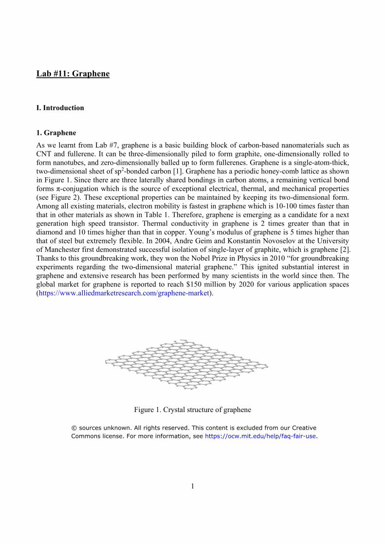
For the first time, Geim and Novoselov used Scotch tape to exfoliate graphene sheets from graphite. Although graphite is composed of vertically-stacked graphene layers, it has been difficult to exfoliate only one layer of graphene from the graphite. Geim and Novoselov picked up the many layers of graphene from the graphite using Scotch tape and then they folded the scotch tape multiple times to reduce the number of layers on the tape. After multiple repetitions of this process, few layers of graphene was bonded to an atomically flat oxidized Si wafer which contains 90 nm SiO2 on the surface. This results in transfer of graphene flakes on SiO2 surface with random distribution of size and layer numbers. Typically the size of graphene flakes is tens of microns, and layer number varies from few layers to monolayer. Although this method is far from industry application, it produces enough monolayered graphene whose physical properties can be characterized. Thanks to the success of this scotch tape method, Geim and Novoselov received the Nobel Prize in Physics in 2010. The entire process flow is depicted in Figure 3 and we will perform the same experiment in Lab #11.
© sources unknown. All rights reserved. This content is excluded from our CreativeCommons license. For more information, see https://ocw.mit.edu/help/faq-fair-use.
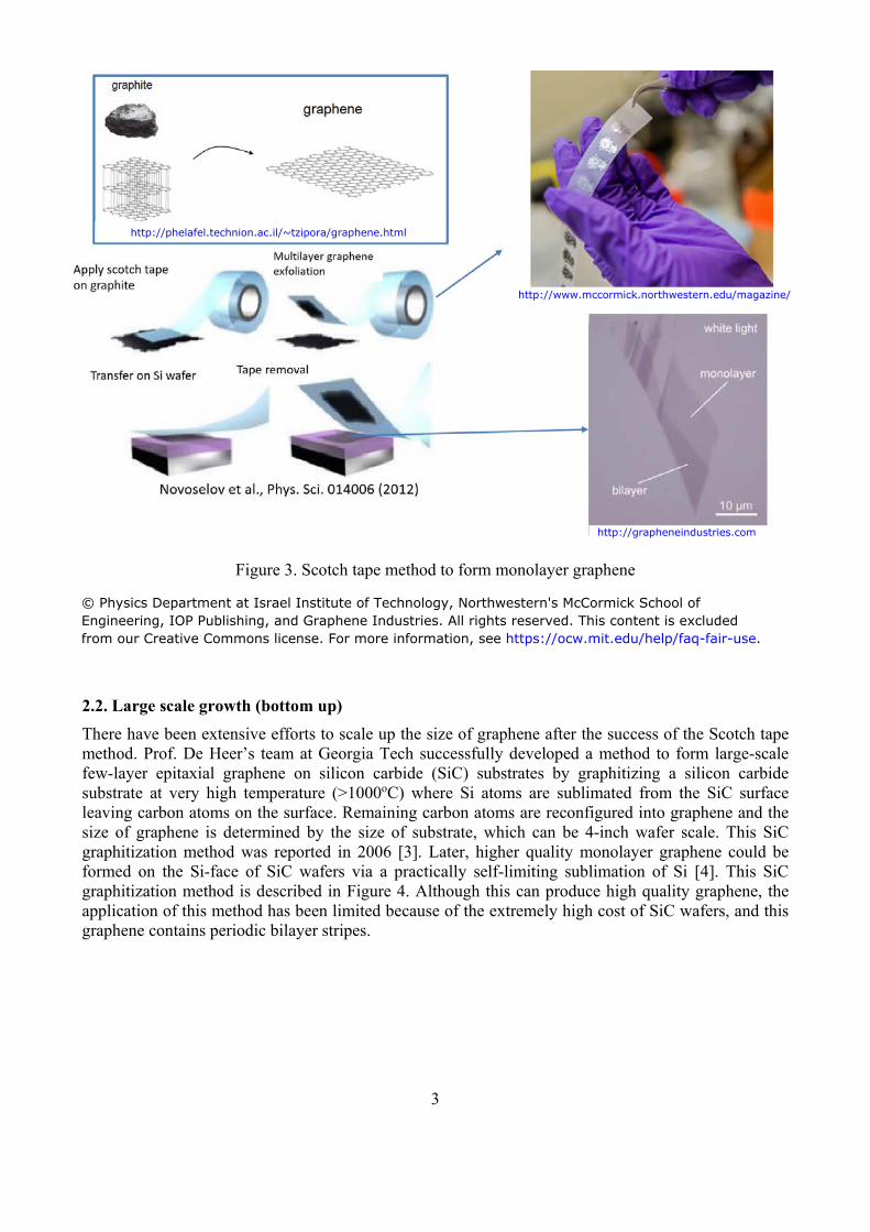
Figure 3. Scotch tape method to form monolayer graphene
© Physics Department at Israel Institute of Technology, Northwestern's McCormick School of Engineering, IOP Publishing, and Graphene Industries. All rights reserved. This content is excludedfrom our Creative Commons license. For more information, see https://ocw.mit.edu/help/faq-fair-use.
2.2. Large scale growth (bottom up)
There have been extensive efforts to scale up the size of graphene after the success of the Scotch tape method. Prof. De Heer’s team at Georgia Tech successfully developed a method to form large-scale few-layer epitaxial graphene on silicon carbide (SiC) substrates by graphitizing a silicon carbide substrate at very high temperature (>1000oC) where Si atoms are sublimated from the SiC surface leaving carbon atoms on the surface. Remaining carbon atoms are reconfigured into graphene and the size of graphene is determined by the size of substrate, which can be 4-inch wafer scale. This SiC graphitization method was reported in 2006 [3]. Later, higher quality monolayer graphene could be formed on the Si-face of SiC wafers via a practically self-limiting sublimation of Si [4]. This SiC graphitization method is described in Figure 4. Although this can produce high quality graphene, the application of this method has been limited because of the extremely high cost of SiC wafers, and this graphene contains periodic bilayer stripes.
3
http://phelafel.technion.ac.il/~tzipora/graphene.html
http://www.mccormick.northwestern.edu/magazine/
http://grapheneindustries.com

4
Figure 4. Method to form epitaxial graphene on SiC
© sources unknown. All rights reserved. This content is excluded from our CreativeCommons license. For more information, see https://ocw.mit.edu/help/faq-fair-use..
This image has been removed due to copyright restrictions.Please see the second image on https://www.comsol.com/blogs/synthesizing-graphene-chemical-vapor-deposition.
Figure 5. Schematics of a process flow for CVD growth of graphene
In 2009, various groups reported large-scale graphene growth on a cheap metal foil via chemical vapor deposition [5,6]. The principle of this method is similar to that of the CNT growth we performed in Lab #7. While we obtained a 1D carbon tube by using a Fe nanosphere seed, we could form 2D graphene by using a planar metal surface as a seed. In the CNT growth, carbon atoms are spontaneously dissolved into metal catalyst and provided to growing CNT. In the graphene growth, the catalytic metal needs to have limited solubility of carbon where the carbon saturates in the metal upon

exposure to a hydrocarbon gas. Typically nickel (Ni) and copper (Cu) films are used as seed films and carbon atoms are saturated in those films at high temperature with methane flow. Upon cooling the substrate, the solubility of carbon in the Ni or Cu decreases and a thin film of carbon precipitated from the surface configures into graphene. The entire metal foils are etched after transferring this graphene to other substrates of interest. The detail about this process is described in Figure 5. This method is an industry-friendly process, as the Ni or Cu foils are cheap and the size of graphene is limited only by the size of the CVD chamber. So far square meter scale graphene has been demonstrated. However, the quality of graphene is poor since the graphene is polycrystalline, graphene is contaminated during the transfer process and CVD graphene contains wrinkles originated from the wet-etch process for removing metal substrates.
2.3. Layer resolved transfer (bottom up + top down)
5
© Science. All rights reserved. This content is excluded from our Creative Commonslicense. For more information, see https://ocw.mit.edu/help/faq-fair-use.
Figure 6. Schematics of process for forming single-crystalline monolayer graphene using layer resolve graphene transfer [7]
Despite having many superior electrical properties, graphene has not had a significant impact in electronics yet because well-ordered, uniform, large grain graphene films cannot be fabricated on conventional semiconducting wafers. CVD growth of graphene on Cu foils has been the mainstream method in manufacturing, but this graphene is polycrystalline in nature with a typical domain size of tens of microns. As mentioned in the last section, high-quality single-oriented graphene can be ensured by forming epitaxial monolayer graphene on SiC surface by self-limiting Si sublimation but the domain size is limited to few microns due to the presence of bilayer stripes at SiC vicinal steps where carrier scattering occurs. In 2013, a method of forming single-crystalline monolayer graphene was reported. This method is called “layer resolved graphene transfer”, where the single-oriented graphene on SiC was exfoliated from the SiC wafer and the bilayer was selectively removed [7]. In this method, the interfacial energy and strain at the graphene/substrate interface can be tuned to enable the transfer

of epitaxial monolayer graphene from SiC as well as the removal of any excess graphene. First, high quality graphene on SiC was exfoliated by depositing Ni films on graphene under high stress (1 GPa). When the strain energy accumulated in the Ni films reaches the interface energy of Ni/SiC, entire graphene films attached to SiC were exfoliated. Second, the excess bilayer stripes were selectively removed by deposing Au films on exfoliated graphene layers, on Ni, where the Au film can selectively pick up the excess bilayers. This happens because the binding energy of Au/Graphene is greater than that of graphene/graphene yielding to separation of graphene/graphene interfaces, and graphene/Ni binding is stronger than Au/graphene binding so that single-crystalline graphene stays well on Ni while Au is picking up bilayer stripes. Figure 6 depicts the detail about this process. This method enables the formation of 4-inch wafer-scale single-crystalline monolayer graphene for the first time (see Figure 7).
6
Figure 7. 4-inch wafer-scale single-crystalline graphene [7]
© Science. All rights reserved. This content is excluded from our Creative Commonslicense. For more information, see https://ocw.mit.edu/help/faq-fair-use.
References
[1] M. J. Allen, V. C. Tung, and R. B. Kaner, Chem. Rev. 110, 132 (2010)
[2] K. S. Novoselov et al., Science 306, 666 (2004)
[3] J. Hass et al, Appl. Phys. Lett. 89, 143106 (2006)
[4] K. V. Emtsev et al., Nat. Mater. 8, 203 (2009)
[5] X. Li et al., Science 324, 1312 (2009)
[6] K. S. Kim et al., Nature 457, 706 (2009)
[7] J. Kim et al., Science 342, 833 (2013)

II. Experimental procedure: Making graphene and observation
In this task, you will
1) Experience Nobel Prize winning method to fabricate graphene from graphite
2) Image different types of graphene using AFM and STM
Part 1: Graphene fabrication
The objective of this section of the lab is to give you the opportunity to experience the Nobel Prize winning method to form graphene and to feel how the innovation was made. As mentioned earlier, monolayer sheets of graphite, which is graphene, could not be made although excellent properties of graphene were already known.
The procedure
A. Apply scotch tape on highly ordered pyrolytic graphite (HOPG) and detach the graphite from HOPG surface.
B. Fold over the Scotch tape several times at different locations to make multiple clones of exfoliated graphite all over the sticky side of tape
C. Repeat B for at least 30 times
D. Place graphite with reduced number of layers on the tape, on the Si substrate and press it hard
E. Detach the tape
F. Observe your sample under the microscope at AFM to see if you successfully transferred graphene on the Si substrate and save the image
Figure 8. Graphene fabrication method using a scotch tape.
Lab #11 Write-Up Questions:
1. (1 point) Present optical micrographs of three types of graphene using optical microscope
attached to AFM and explain the strength/weakness of each method.
7

Part 2: Measure the thickness of graphene using AFM
I. The procedure
A. Locate CVD graphene (see section 2.2) and single-crystalline graphene (see section 2.3) under the microscope attached to AFM
B. Save images of CVD graphene and single-crystalline graphene and compare morphological difference
C. Locate AFM tip at the crack in single-crystalline graphene
D. Approach tip to the crack area and scan from the crack to graphene
E. Process the image by following the procedure described in Short Guide to the TT-AFM in section II below
F. Measure the height of graphene
G. Locate flake graphene you made under the microscope attached to AFM
H. Save image of flake graphene
I. Locate AFM tip on the graphene flake
J. Approach tip to the graphene flake and scan from the flake to the outside of flake
K. Process the image by following the procedure described in Short Guide to the TT-AFM in section II below
L. Measure the height of flake graphene you made
M. Repeat I-L until you find reasonably thin graphene (few nanometer thick)
N. Estimate number of graphene layers in your flake graphene
Lab #11 Write-Up Questions:
2. (2 point) Present AFM image of single-crystalline graphene and estimate graphene thickness of graphene
3. (2 point) Present AFM image of flake graphene. What is the minimum thickness that you could achieve? (extra 1 point for showing monolayer graphene)
4. (1 point) Estimate number of layers of your graphene flakes transferred on Si wafer
5. (2 point) Can you exfoliate only one graphene sheet from HOPG? Explain why?
8

II. Short Guide to the TT-AFM This section is to guide you through running a sample on the TT-AFM by AFM Workshop. You should scan one sample with full parameter settings and repeat the measurement using high resolution settings. Turn on Equipment
‐ Turn on by the switch on back, LEDs turn on ‐ Take off lens cap from optics ‐ Turn on LED illuminator with the on switch
Open Programs- C Drive, AFM Equipment ‐ 2.0.3 50 Micron Scanner shortcut ‐ USB 2.0 Camera ‐ Start camera by hitting play button on upper left
o Should see probe
Probe Exchange ‐ Raise tip from sample; click and hold the up button in manual ‐ z motor control ‐ Increase slider bar for speed to raise it
o Hear motor running to know it’s moving o In camera, probe will go out of focus as it goes away from sample
‐ Alternative: Use knob on the back of the box o Spin clockwise to raise tip
‐ Once you’re about 1 cm from surface it is safe to remove tip: Grab holder and pull straight out. Flip over so clip is on top
‐ Set down probe exchange tool on the counter ‐ Line up holder with probe exchange tool- line up hole & the raised up portion of the probe exchange
tool- the bolt will line up and fit snug & smooth o Don’t force it down o Hold so clip is facing you & push down on the sides, allowing probe to slide out, give a few
gentle taps and probe will slide out ‐ Give a few taps so probe is in the oval section ‐ Using fine tipped tweezers, remove the old probe and put it back in the gel pack ‐ Take a new probe and place it into the oval, so that the back end of the probe is in the track ‐ Do the opposite of how to remove. Push down on sides and tilt it back, give a few gentle tips
o Don’t tilt too hard, this may cause probe to fall to quickly and damage the tip o Set it on the table, push down, and tap. Giving some vibrations will let probe seat on its own
‐ Turn holder over and slide back in place under the copper clips. It should slide easily without needing much force.
Align AFM
‐ First, find probe with the camera o Use focus knob and camera zoom to find probe on camera viewer
Turn focus knob clockwise to right until it stops bringing the camera all the way up Turn knob to left until see probe in the camera viewer
9
Figure 9: TT-AFM

o Center the probe in the camera using knobs on the stage that the camera is mounted on ‐ Center the probe over the scanning area
o Mark position of the probe using the “circle” tool (circle with red dot in the center) Click on the center of the cantilever tip & draw a circle outwards
o Focus on the scanning surface by moving the camera down (turning the knob counterclockwise to the left) Watch camera viewer until scanning area comes into focus
o Move the sample stage with the 2 knobs to move the sample so that the cantilever tip (marked by the circle) is located in the middle of the sample If sample is not centered, the scanned image will be tilted
‐ Align the laser: Adjust focus again and find the cantilever (See Figure 10 for this section) o Now that sample is centered under the cantilever we can get rid of the circle – click on
“undo” a left pointing arrow button o Make sure laser power is on- on prescan tab, Laser Power should say on- look for red glow
of the laser o Move the laser to the tip of the cantilever by rotating the knobs on the laser holder o Adjust detector by rotating the knobs on the detector holder
Look at beam position graph & data in the PreScan window Want vertical = 0.4, horizontal = 0 (close is fine, need not be perfect)
Load a Sample & Start the Scan
‐ Should have: probe in AFM, laser aligned, detector aligned, system centered in camera ‐ Select Mode: in PreScan tab of software, pick vibrating or non-vibrating
o For topography scans, choose vibrating o Click on Scan Mode window & select vibrating
‐ For vibrating mode, need to tune frequency- go to Tune Frequency section of PreScan tab o Look at tips box and read resonant frequencies
Sweep over that range to find resonant frequency of the tip First run, steps at 40-50 to find frequency Done, see a tip- click and drag red and green lines around peak and scan again with
more steps to get better measurement (75 steps) o Y axis is amplitude in volts- peak value should not be more than 1.4V or less than 0.4V
10
Figure 10: TT-AFM Laser spot

Adjust if high or low- if high, lower demod gain If demod is as low as goes, can change amplitude Vpp gain,
Re-run scan Blue line is what we select as our actual resonance
To ensure the tip doesn’t get damaged, the blue line should be set at about 80% of the way up on the left side of the peak
Program should select close to that Peak should be below 1.4V
Check phase that has an inflection point near the peak Can read off the selected resonance for the probe in Frequency Select box
o Do Range Check Move tip up so that tip doesn’t contact anything (about 1.5 cm space between tip &
holder) Prescan Tab, Range Check, Click Start
Program ramps Voltage up on x/y piezo so we can scan linearly If don’t range check, can get strange scans
o Load sample Make sure tip is far from sample holder (2 cm between probe & sample holder) Use z control, turn clockwise to move it up Using tweezer, grab the disk, and move it to sample holder
Will feel it snap in place when magnet catches Push it into the center
Look in camera, use focus knob to focus clearly on the sample o Tip Approach
Use Z control, counterclockwise, so tip goes down, until tip is within 1 cm of sample Use software to move rest of the way
Use Manual Z Motor Control Box Set Speed (maybe around 0.3), hold “down”, watch and see it come close See by eye and by camera will see tip start to come into focus
Want to get sample in focus and tip just out of focus, then do automated tip approach Set speed to 0 Go down slowly, don’t crash tip into sample! Look at laser reflection off the tip, when tip is on the surface, laser reflection
will be right under tip, so keep moving until spot is close to under the tip (not all the way- let software bring tip into contact)
Start automated tip approach o Go to system tab and check parameters o Tip approach parameters- don’t set integral above 800 (600 is good)
Z parameters- z HV gain- 15 is as high as it can go (fastest), lower will
o Hit start, once done, “In Feedback” light will be green which means the tip is engaged with the sample Can lower Setpoint (mV) in 10s place slowly and shouldn’t see
Z Drive (V) change because we’re engaged with surface o Want the z drive V to be at 0, use Z center button
11

If Z drive is below, click up a few times and re-do automated tip approach
If Z drive is above, use Re-Center button In Z Feedback, Integral set to 100 Click Re-Center Yellow indicator should be close to 0
‐ Do Scan! o Go to Topo Scan
Set z feedback integral back to 1000 Adjust Scan Setup Parameters
Scan rate 0.5Hz, Scan lines 256 (fast) Left Image will be Z_DRIVE (this is the image) Right Image will be Z_ERR (shows any drastic changes in topography)
o Click Start under Scan High Resolution Scanning In order to see small features, one needs to turn down the XY parameters, located under the “System” tab. The “full parameter” settings are as follows:
X Gain (%): 100 X Proportional: 256 X Integral: 4096 X Derivative: 0 Y Gain (%): 100 Y Proportional: 256 Y Integral: 4096 Y Derivative: 0
These should be changed to the following high resolution settings:
X Gain (%): 0 or 10 X Proportional: 0 X Integral: 96 X Derivative: 0 Y Gain (%): 0 or 10 (just be consistent with your X Gain (%) setting!) Y Proportional: 0 Y Integral: 96 Y Derivative: 0
The X and Y Gain (%) are the strain gauges, and can add a lot of noise to the measurement. They can be turned down or off when the XY HV Gain is turned down below 5. The Z HV Gain can also be turned down between 3 and 5 to reduce noise as well. Once these parameters are lowered, one may scan small areas below 5 x 5 microns and observe details that would be missed under the full parameter settings. Image Analysis using Gwyddion software
12

Gwyddion is a free and open source software used primarily for the analysis of scanning probe microscopy data. You may download the software and read the full documentation at: http://gwyddion.net/The analysis for this is lab should be basic and straightforward. Open your image file in Gwyddion. At a minimum, it will be necessary to level your image using a mean plane subtraction. Then you may easily measure features in the image.
‐ Open file ‐ Level data by mean plane subtraction or other data processing if needed ‐ Measure feature profiles
13

Part 3: Imaging atomic arrangement of HOPG using STM
The Scanning Tunneling Microscope (STM) is a delicate instrument and care is required during operation and handling. The shiny metal holder must not be touched even with gloves as it is a
14
critical component of the positioning system. The tip is very sharp and must be handled carefully. Operate the STM only under direct supervision of your instructors.
Lab #11 Write-Up Questions:
6. (2 point) Present STM surface topology of graphene and explain the difference between AFM and STM for imaging graphene
I. Introduction to the Scanning Tunneling Microscope (STM)
The STM was invented by Gerd Binnig, Heinrich Rohrer and colleagues in 1981, which earned Binning and Rohrer the Nobel Prize in Physics in 1986. Scanning tunneling microscopy1-3 is among the very few techniques (examples of others being AFM and TEM) that allow for imaging and manipulation with atomic-scale resolution. It belongs to the broad category of techniques known as scanning probe microscopy, where a probe is scanned over a surface4. Examples of scanning probe microscopy are atomic force microscopy5 (which we will see in the next lab module), scanning thermal microscopy6, and near-field scanning optical microscopy7.
The STM uses a small tunneling current between a sharp tip and the surface of an electrically conductive sample to image and analyze the sample. Occurrence of this tunneling current is a quantum-mechanical effect, where a driving voltage across the tip-sample gap results in a current that decays exponentially with the tip-sample separation distance. The current depends on the tip-sample gap, tip geometry, electron densities and energy states of electrons in the tip, among other factors1. The theory describing this current is very complex and beyond the scope of this course. The exponential dependence of current on the tip-sample gap enables high-resolution scanning of surface topography: A current value is set (typically for a gap of 1 nm or less), and the tip is scanned in X and Y directions across the sample while changing the height of the tip above the sample (Z direction) using a feedback control loop that maintains the current. The Z height map yields the topography of the sample surface where a constant tunneling current is maintained (Figure 1). To implement this technique, the STM comprises a high-resolution scanner (typically a piezoelectric tube scanner), a sharp tip prepared by cutting or etching, a feedback controller, vibration isolation system, and a computer to record and display the height information. While the STM can work in ambient air, the temperature needs to be stable and the environment is often controlled, e.g. ultra-high vacuum may be used. With a tip terminating in one or two atoms, sub-atomic lateral resolution and even better height resolution can be obtained.

15
Figure 11. Schematic diagram of the STM.
This image has been removed due to copyright restrictions.Please see Figure 3 on http://conf.ncku.edu.tw/research/articles/e/20080606/5.html.
© IBM. All rights reserved. This content is excluded from our Creative Commonslicense. For more information, see https://ocw.mit.edu/help/faq-fair-use.
Figure 12. Left: Image of “IBM” written with xenon atoms on nickel using an STM. Right: Creation of a “quantum corral” using 48 atoms of iron on a copper substrate. The “corral” changes the quantum states of the electrons, resulting in a clearly evident standing wave structure that can be theoretically predicted. Courtesy of IBM gallery.
The STM can also be used to manipulate single atoms: when the current between the tip and an atom on the surface is increased, it creates a temporary bond that allows the tip to move the atoms. A famous early example is the celebrated “IBM” written with xenon atoms (Figure 2). Another striking example is the creation of a “quantum corral” by manipulation of iron atoms. A circular arrangement of iron atoms resulted in observation of standing electron waves inside the circle! These images illustrate the power of scanning tunneling microscopy to manipulate atoms and study electronic states with high resolution. The STM now finds wide use for measuring electronic states in semiconductor and surface physics, studying chemical reactions in catalysis, characterizing metal and alloy surfaces, and observing biomolecules on surfaces.

II. Laboratory Objectives
In this laboratory, we will a) get hands-on experience operating an STM, and b) image the surface of graphite using the STM. The instrument that we will use is an educational easyScan 2 STM made by Nanoscience Instruments. Our goal will be to image individual carbon atoms on the graphite surface and to figure out the parameters of the hexagonal arrangement of atoms on the graphite surface. This is the only instrument in the 2.674 laboratory capable of achieving atomic scale resolution.
III. Experimental1 A. Introduction to the Nanosurf easyScan 2 STM
16
The Nanosurf easyScan 2 STM is an educational instrument designed to allow people without a high level of expertise to perform experiments. The main components of the system are (Figure 3):
1. easyScan 2 Controller 2. easyScan 2 STM Scan Head 3. Magnifying cover with 10× magnifier 4. Vibration isolation platform
1 Parts of this manual are adapted or reproduced from the EasyScan 2 STM Operating Instructions Version 2.2 prepared by Nanoscience Instruments Inc, 2011.
Scan head Cover Vibration isolation platform
Controller
Figure 13. Main components of the easyScan 2 STM.
© sources unknown. All rights reserved. This content is excluded from our CreativeCommons license. For more information, see https://ocw.mit.edu/help/faq-fair-use.

The controller has status indicator lights to indicate the status of the probe tip, controller configuration, and scanning head. All status lights on top of the controller will light up for one second when the power is turned on.
a) Probe status light: Indicates the status of the Z-feedback (direction perpendicular to the sample surface) loop. The Probe Status light can be in any of the following states:
a. Red: The scanner is in its upper limit position. This occurs when the tip–sample interaction is stronger than the set point for some time. There is danger of damaging the tip due to an interaction that is too strong.
b. Orange/yellow: The scanner is in its lower limit position. This occurs when the tip–sample interaction is weaker than the set point for some time. The tip is probably not in contact with the sample surface.
c. Green: The scanner is not in a limit position, and the feedback loop can measure the sample surface.
d. Blinking green: The feedback loop has been turned off in the software. b) Scan head lights: Indicate the scan head type that is connected to the instrument. The
scan head lights blink when no scan head can be detected, or when the controller has not been initialized yet.
c) Module lights: Indicate the modules that are built in into the controller. The module lights blink when the controller has not been initialized yet. During initialization, the module lights are turned on one after the other.
B. Preparing the STM for measurement
17
The STM controller should be connected to the scan head with the provided connector, with the computer by the USB connector, and to the mains power supply. B. 1 Initializing the controller:
1. Make sure that the easyScan 2 controller is connected to the mains power and to the USB port of the control computer.
2. Turn on the power of the easyScan 2 controller. First all status lights on top of the controller briefly light up. Then the scan head lights and the lights of the detected modules will start blinking, and all other status lights turn off.
3. Start the easyScan 2 software on the control computer. The main program window appears, and all status lights are turned off. Now a message “Controller Startup in progress” is displayed on the computer screen, and the module lights are turned on one after the other. When initialization is completed, a message “Starting System” is briefly displayed on the computer screen, and the probe status light, the scan head status light of the detected scan head, and the module lights of the detected modules will light up. If no scan head is detected, both scan head status lights blink.
B. 2 Preparing and installing the STM tip: The STM tip needs to be prepared and installed, which is the most difficult part of the
preparations. A 0.25 mm diameter Pt/Ir wire is provided for making the tips. It usually needs patience and some practice to get the first good tip. Only an accurately cut tip enables optimal measurements. Therefore, cutting and installing should be carried out with great care.

Before cutting the tip: 1. Clean the cutting part of the provided wire cutters, the flat nose pliers, and the pointed tweezers
with ethanol. Use only these tools to touch the Pt/Ir wire. 2. Remove the old tip from the instrument using the pointed tweezers. If the tip wire is still long
enough, you may try to cut the same wire again, otherwise cut the Pt/Ir wire. To prepare the tip:
1. Hold the end of the wire firmly with the pliers. 2. Move the cutters at a length of approximately 4 mm, as obliquely as possible (Figure 4). 3. Close the cutters until you can feel the wire, but do not cut the wire. 4. Pull in the direction shown in
Figure 4. The tip needs to be torn off rather than cleanly cut through, in order to obtain the required tip sharpness.
5. Use the pointed tweezers to hold the tip wire with just behind the tip.
6. Release the flat pliers.
This process mechanically shears the Pt/Ir wire, resulting in a sharp tip capable of providing atomic scale resolution. Pt/Ir wire is used because it resists oxidation and Ir increases the stiffness8. However, the shape of the wire where it is sheared is difficult to control, and such tips are not suitable for imaging high aspect ratio features. IMPORTANT:
Never touch the end of the tip with anything. Ensure that the tip wire is straight. Do not twist the tip clamp in any way, nor lift it too high.
To mount and unmount the tip:
1. Put the tip wire on the tip holder parallel to the groove in the tip holder, so that it crosses below the tip clamp (Figure 5A).
2. Move the tip wire sideways until it is in the groove in the tip holder (Figure 5B).
3. The freshly cut tip should be securely held under the clamp and extend about 2–3 mm beyond the tip holder. The tip is now installed.
B. 3 Preparing and installing the sample:
18
Figure 14. Cutting the STM tip.
Figure 15. Mounting the STM tip.

The STM can be used to examine electrically conductive materials. In practice, however, the choice of material is more limited, because the surface of the sample must be totally clean and mirror-like to obtain useful results, and it must be in a non-oxidized state to be conductive. Because of this, some samples need special preparation. In this lab, we will use a 5 mm x 5 mm highly oriented pyrolytic graphite (HOPG) sample (mounted on magnetic steel disc galvanized with nickel) provided by Nanoscience Inc. The surface of the graphite sample can be cleaned when it is very dirty or uneven. Due to the layered structure of graphite this can easily be done using a piece of adhesive tape. IMPORTANT Never touch the sample surface once it is prepared. To prepare the sample:
1. Put the sample on the table using a pair of tweezers. 2. Stick a piece of adhesive tape gently to the graphite and then pull it off again. The topmost
layer of the sample should stick to the tape. 3. Remove any loose flakes with the tweezers.
The graphite sample is now ready for use and should not be touched anymore. To mount the sample (Figure 6):
1. Unpack the sample holder, touching only its black plastic handle. 2. Put the prepared sample onto the magnetic end of the sample holder using a pair of tweezers. 3. Place the sample holder carefully in the scan head so that it doesn’t touch the tip, and in such a
way that the sample is not pulled from the sample holder by the magnet that holds the sample holder in place.
4. Put the sample holder down on to the sample holder guide bars first and release it gently on to the approach motor’s support.
C. Imaging the surface of graphite using the STM
19
C.1 Starting up:
This image has been removed due to copyright restrictions.Please see Rys. 6 on http://www.serwisy.umcs.lublin.pl/mlpar/11_stm/stm.htm.
Figure 16. A) Putting the sample on the sample holder. B) Placing the sample holder in the scan head.
C.1 Starting up:
This image has been removed due to copyright restrictions.Please see Rys. 7 on http://www.serwisy.umcs.lublin.pl/mlpar/11_stm/stm.htm.

Switch on the controller (the switch is located at the back) after installing the sample and connecting the controller to the scan head, computer, and mains power supply. Start the easyScan 2 software. The software can run in simulation mode that can be toggled using OptionsSimulate microscope. Make sure that the STM is not running in simulation mode. To load the correct STM configuration, do the following:
1. Open the User interface dialog via the menu OptionsConfig User Interface…
2. Select the “Easy level” user interface mode. 3. Open the menu item FileParametersLoad.., and
load the file “Default_EZ2-STM.par” from the directory that holds the default easyScan 2 configurations (usually C:\Program Files\Nanosurf\Nansurf easyScan 2 software\Config).
C.2 Approaching the tip to the sample: To start measuring, the sample must be very close to the tip to enable a tunneling current to
flow. Approaching the tip to within this small distance is a delicate operation carried out in three steps as follows. The status light indicates the current status of approach as described above.
1. Manual coarse approach: In this step, the sample surface is brought close enough to the tip by hand to allow further motorized approach afterwards.
a. Push the sample holder carefully to within 1 mm distance of the tip. b. If the tip is pointing toward a rough area of the sample, try turning the sample holder
around its axis so that the tip points towards a flat, mirror-like area of the sample. c. Put the magnifying cover over the scan head without touching the sample holder.
20
d. Place the magnifier in such a way that you can see the mirror image of the tip in the sample.
e. The cover reduces air flow around the scan head and reduces thermal drift in measurements at atomic scale.
2. Manual approach using the approach motor: In this step, the sample surface is brought as close to the tip as possible, without touching it. The closer the two are together, the less time the automatic final approach takes.
a. Watch the distance between tip and sample with help of the magnifier. b. Click “Advance” in the approach panel to move the sample to within a fraction of a
millimeter of tip. You should only just be able to see the gap between the tip and its mirror image (Figure 7). The smallest visible gap depends on the observation angle of the magnifier and the illumination of the sample.
c. If you cannot see the motor moving, the sample holder and guide bars are dirty and must be cleaned using ethanol as described in the manual.
3. Automatic final approach: In this last step, the sample automatically approaches the tip until a given set point is reached. First check that the set point and the feedback speed are set properly.
a. Open the Z-Controller Panel in the Navigator. b. Set “Set point” (tunneling current) to 1.00 nA.
Figure 17. Position of tip at the end of manual approach with the approach
motor. © sources unknown. All rights reserved. Thiscontent is excluded from our Creative Commonslicense. For more information, see https://ocw.mit.edu/help/faq-fair-use.

c. Set “Loop gain” (the speed of the feedback loop) to 2000. d. Set “Tip voltage” (tip–sample-voltage) to 50 mV. e. Now that the set point and feedback settings are correct, start the automatic final
approach by clicking on the “Approach” button in the positioning window. The sample holder is now moved towards the tip by the approach motor. After each step, the Z-scanner is fully retracted from the sample, and released to move towards the sample. The approach is finished if the current determined by set point is detected before reaching the maximum extension of the Z-scanner, otherwise the approach motor will continue with the next step. Due to the motion of the Z-scanner, the probe status light will blink red–green–orange/yellow in cycles. When the approach has finished successfully, the probe status light changes from a blinking state to a constant green, and the message box “Approach done” appears.
f. Click “OK”.
If the status light changes to red instead of green, or if the approach has not finished after 10–20 seconds, try to decrease the tip–sample distance a little more using manual operation of the approach motor. C.3 Starting a measurement:
Now that the tunneling current defined by the set point is flowing between tip and sample, the instrument is ready to start measuring. By default, the instrument is set to automatically start measuring after the automatic approach. Alternatively, you can start the measurement using the toolbar at the top of the imaging panel. If the preparation of the tip and sample and the approach were successful, images of the measurement will show a more or less straight line in the line graph (Figure 8) and a plane in the color map. The default method of measurement is to maintain a constant current and scan the topography, called the constant current mode. Watch the displays for a while until the color map image has been drawn about three times. A “nervous” line in the line graph indicates a bad tunneling contact. Usually this is caused by the tip being too blunt or instable. This means that you should stop measuring and cut a new tip. If the line in the line graph is calm and reproduces consistently, you can continue with the measurement. C.4 Obtaining atomic resolution:
To observe individual atoms, the size of the scanning region should be decreased to about 5 nm or below. The size can be decreased by using the zoom button in the toolbar, or by setting the desired size in the imaging panel. Try to
21
Figure 18. Starting image showing a good line graph (left) and a “nervous” line
graph (right).
© sources unknown. All rights reserved. This content is excluded from our CreativeCommons license. For more information, see https://ocw.mit.edu/help/faq-fair-use.

zoom in on a region that appears relatively flat. To minimize thermal drift effects, set the time/line to about 0.06 s. In case the line graph is not level, you can automatically level it by clicking on the “Set” button in the imaging options of the imaging panel.
IMPORTANT Measurements on the micrometer/nanometer scale are very sensitive to environment influences. Direct light or fast movements - causing air flow and temperature variations near the scan head - can influence and disturb the measurement. It is best to let a promising measurement run for some time in order to stabilize thermally.
In a good color map chart of graphite you will see a pattern consisting of bright, intermediate,
and dark spots. It looks like a three dimensional image of balls lying next to each other, but be careful: these are not the single atoms! To interpret the image correctly you must first be aware that bright spots show high points and dark spots low ones. In the lattice model of graphite (Figure 9) one can see that there are two different positions of the carbon atoms in the graphite crystal lattice: one with a neighboring atom in the plane below (gray) and one without a neighbor in the lattice below (white). As a consequence, the electrical conductivity of the graphite surface slightly varies locally, so that the atoms without neighbors appear higher than the others. This also causes the lattice constant between the bright “hills” to have the higher than normal value of 0.25 nm (From the easyScan 2 Manual). C. Storing the measurement:
When you are satisfied with your image and would like to keep it, you can take a snapshot of it by clicking the “Photo” button. The behavior of this button depends on whether a measurement is in progress or not:
1. When a measurement is in progress and is activated, a copy of the measurement is made to a measurement document after the measurement is finished.
2. When the measurement is not in progress and is activated, a copy is made immediately. If you want to save the new measurement document to your hard disk drive, activate the
measurement document by clicking in its window, or by selecting it in the Windows menu. Then use FileSave as... to store the measurement for later viewing or analysis with the easyScan 2 STM
software.
This image has been removed due to copyright restrictions.Please see Rys. 7 on http://www.azonano.com/work/HqxW2qp0cG7XAG813H59_files/image004.jpg.
Figure 19. The graphite surface showing measurement (left) and lattice model (right).
22
This image has been removed due to copyright restrictions.Please see Rys. 8 on http://www.serwisy.umcs.lublin.pl/mlpar/11_stm/stm.htm.

Record the color map and line scan with scan size of ~1-2 nm (zoomed in) and ~5 nm (zoomed out), with scan time/line of 0.06 s and a long scan time/line of ~0.2 s.
D. Finishing up First stop the measurement using the “Stop” button. To move the tip away from the sample, first use the “Withdraw” button and then “Retract”. Once the sample is a safe distance away from the tip, the sample holder can be removed. The sample must be stored in its box, and the sample holder must be stored in its container. Now you can shut down the easyScan 2 control software and turn off the controller.
23

MIT OpenCourseWarehttps://ocw.mit.edu
2.674 / 2.675 Micro/Nano Engineering LaboratorySpring 2016
For information about citing these materials or our Terms of Use, visit: https://ocw.mit.edu/terms.

![Atomic Structure of Graphene and h-BN Layers and Their ...€¦ · graphene [22]. High angle annular dark field (HAADF) imaging was employed to produce micrographs. This chemically-sensitive](https://static.fdocuments.net/doc/165x107/5f170a12663073087048d69b/atomic-structure-of-graphene-and-h-bn-layers-and-their-graphene-22-high-angle.jpg)