JOSEPHSON CIRCUITS FOR PROTECTED QUANTUM BITS
165
JOSEPHSON CIRCUITS FOR PROTECTED QUANTUM BITS by WEN-SEN LU A dissertation submitted to the School of Graduate Studies Rutgers, The State University of New Jersey In partial fulfillment of the requirements For the degree of Doctor of Philosophy Graduate Program in Physics and Astronomy Written under the direction of Michael Gershenson And approved by ____________________________________________________ ____________________________________________________ ____________________________________________________ ____________________________________________________ ____________________________________________________ New Brunswick, New Jersey May 2021
Transcript of JOSEPHSON CIRCUITS FOR PROTECTED QUANTUM BITS
JOSEPHSON CIRCUITS
FOR PROTECTED QUANTUM BITS
by
WEN-SEN LU
A dissertation submitted to the
School of Graduate Studies
Rutgers, The State University of New Jersey
In partial fulfillment of the requirements
For the degree of
Doctor of Philosophy
Graduate Program in Physics and Astronomy
Written under the direction of
Michael Gershenson
And approved by
____________________________________________________
____________________________________________________
____________________________________________________
____________________________________________________
____________________________________________________
New Brunswick, New Jersey
May 2021

ii
ABSTRACT OF THE DISSERTATION
Josephson circuits for protected quantum bits
by WEN-SEN LU
Dissertation Director
Michael Gershenson
Over the past two decades the performance of superconducting quantum bits (qubits)
has been improved: the coherence time of individual qubits has been increased by five
orders of magnitude, from a few nanoseconds to > 100 μs. The much-improved energy
relaxation time, scalability from engineering point of view, and compatibility with
microwave control make superconducting qubits one of the major competitors for quantum
information hardware applications. Despite the progress, experimental realization of
quantum error corrections for logical qubits remains challenging.
One of possible solutions to this problem is the development of so-called protected
qubits whose errors would be suppressed by special symmetries of the underlying
Hamiltonian. The realization of such qubits requires elements not found in the conventional
superconducting circuit toolbox, such as Josephson elements with cos(
) and cos(2)
dependences of the Josephson energy on the phase difference , circuits with a very
large kinetic inductance, and junctions with unusually low .

iii
This thesis focuses on design, fabrication and characterization of circuits based on
low- Josephson junctions (JJs) and superinductors (SIs). By analyzing limitations on the
junction performance imposed by the thermally activated phase slips, we observed a
dramatic reduction of the critical currents in the regime ≤ which was accompanied
by an increase of the zero-bias resistance . The first part of this work provides practical
considerations for the use of such junctions in quantum circuits. With the aim of improving
elements with a very high kinetic inductance, in the second part we developed
superinductors based on the granular Aluminum ( ) films, in which Josephson
junctions are realized between nanoscale grains. The circuits based on such SIs
demonstrate low microwave losses at ultra-low temperatures. Superinductors are an
essential element of a novel qubit that we have developed – the so-called bifluxon. The
qubit consists of a Cooper-pair box (CPB) with low- Josephson junctions shunted by a
superinductor, thus forming a superconducting loop. When the loop is threaded by the
magnetic flux Φ = Φ 2⁄ where Φ is the flux quantum, the qubit offers exponential
suppression of energy decay from charge and flux noises, and dephasing from flux noise.
In the last part of this work, we observed an increase of the energy relaxation time by two
orders of magnitude, up to 100μs, by turning on protection in the bifluxon qubit.

iv
DEDICATION
It has been quite a journey to reach this personal milestone, with all the supports
along the way. I started it with a simple wish that before I was fully trapped by routine
works in the industry, I wanted to spend the last part of my youth learning from and
contributing to frontier research involving quantum engineering and microwave electronics,
I am deeply grateful that today I ended up with much more than I was expecting.
I would like to start with thanking Professor Michael Gershenson (Misha) for his
mentorship throughout this work. As an old mandarin saying goes, he who teaches us for
one day is our father for life. Misha has always been a keen experimentalist, a resourceful
mentor, and a great friend. Indeed, in addition to scientific skills, the most valuable traits I
learnt from the interactions with him is diligently polishing everything. With patience we
polished fabrication recipes, theoretical pictures behind literatures, to scientific writings.
There will be no shine until we spent time really sitting down and polishing down to the
details. Every sentence in this thesis is written under his guidance and influences, one way
or another. I deeply appreciated the opportunity to have him as my mentor.
As another brilliant experimentalist and thinker in our lab, Dr. Konstantin
Kalashnikov always provides me his valuable microwave expertise and extensive data
analysis tools such as python packages and theoretical modeling. I sincerely thank him for

v
his direct contribution and fruitful discussions steering the direction of bifluxon qubits. In
the meanwhile, a special acknowledgement is due to Plamen Kamenov, who diligently kept
our nano-fabrication process consistent and reliable. I admire his attentive attitude, which
later became one of the foundations of this work. Speaking of the foundation, a special
thanks is given to Wenyuan Zhang for her path finding works guiding this thesis. Her
knowledge in microwave electronics and python toolkits are also essential to this work. I
would also like to thank Thomas DiNapoli for encouraging discussions and idea exchange
for this work, which greatly improved my thinking process.
In a separate paragraph I thank Professor Matthew Bell for his pioneering works
from bifluxon qubit experiments to the infrastructure in our lab that I extensively used
during the past years. Nearly all experimentalists would agree that “just keep the tool
running” cruelly simplified the efforts and times from a researcher at the frontline, and
without his solid experience and extensive familiarity to our equipment the experimental
part of this work would never be realized. Even though we did not overlap, his prior efforts
and inputs provide a solid foundation for this work. His influence on this work is ubiquitous.
I would also like to express my appreciations to microwave engineering experience
exchange with energetic scholars Professor Michael Wu, Professor Srivatsan Chakram
Sundar, and Dr. Xiaoyue Jin. They have been invaluable sources of my microwave

vi
knowledgebase. I appreciate the chance to coach and work with young minds during the
past few years including Darren Schachter, Brian Lerner, Shuping Lee, and Mohamed
Zeineldin. By completing various toolkits in the lab we learnt a great deal from each other.
I would also like to thank the supports from Yuriy Streltsov and William Schneider for
their continuous helps from electronic to machining requests from us.
Also, I would like to thank those brilliant minds that I had privilege to work jointly
in the past, in particular Dr. Takane Kobayashi, Dr. Leila Kasaei, Dr. Hussein Hijazi, and
Professor Leonard Feldman on the granular aluminum engineered with helium ion beam
lithography projects. It is quite impressive to see the other end of frontier fabrication
spectrum such as ion beam lithography, and I sincerely hope with the continuous efforts
this technology can soon be leveraged to improve the performance of superconducting
circuits. I thank all members of Eva’s lab, in particular Dr. Junxi Duan, Xinyuan Lai, Dr.
Shaung Wu, Zenyuan Zhang, Nikhil Tilak, Dr. Jinhai Mao, and Professor Eva Andrei, for
being our faithful and resourceful neighbors. From vacuum gaskets to atomic force
microscopy. their proximity and availability were keys to our experimental works. I would
also like to give my deep appreciation to Professor Vitaly Podozorov for providing his
invaluable insights and offering tools during our difficult times.
vii
I would also like to thank my committee members Professor Salur, Professor
Bartynski, Professor Kotliar, and Dr. Chii-Dong Chen, for their precious inputs and
guidance on my thesis writings. I also thanks Jerrell Spotwood, Shirley Hinds, Nancy
Pamula, and Professor Ronald Gilman for their continuous administrative supports and
efforts in the past few years such that I can focus on the scientific part of my study.
I also appreciated the fruitful brainstorms among various occasions with the great
minds in the same building, Dr. Po-Yao Chang, Hsiang-His Kung. Dr. Li-Cheng Tsai,
Ghanashyam Khanal, and Conan Huang. They had provided solid sources for inspirations
which benefit my research.
Finally, I would like to end this important section by echoing the last statement in
the opening paragraph. I pursued my PhD with the aim of extending my engineering
toolbox, and I am deeply grateful that I ended up with growing not only intellectually but
also mentally. By taking up the responsibility with Tammy as being parents, I am truly
thankful to have Willow as our little monster and form a wonderful family. With the on-
going pandemic, the last part of this work can never be done without Tammy’s great
attention and continuous supports in my life.
With all the scientific efforts, dedications, friendships, and loves, here I humbly
present this work to everyone I have the privilege to work with and live with.

viii
Table of Contents
ABSTRACT OF THE DISSERTATION ................................................................ ii
DEDICATION ............................................................................................................... iv
CHAPTERS
Chapter I : Introduction ..................................................................................................1
I.1The Josephson phenomena and modeling of Josephson junctions ......................3
I.2The phase-slip dynamics of a Josephson junction ...............................................6
I.3The current-voltage characteristics of a Josephson junction .............................10
I.4The phase diffusion regime in underdamped junctions .....................................13
I.5Kinetic inductance .............................................................................................15
I.6The non-linear inductance of a Josephson junction ...........................................18
I.7Theory for fluxon-parity protected circuits .......................................................19
I.8Components for fluxon-parity protected circuits...............................................22
I.9Thesis overview .................................................................................................25
Methodology ..............................................................................................27
II.1Fabrication ........................................................................................................27
II.1-1 Lithography ....................................................................................28
II.1-2 Film deposition and junction fabrication .......................................33
II.1-3 Process flows .................................................................................39
II.2Measurement ....................................................................................................42
II.2-1 DC measurement ............................................................................42
II.2-2 MW measurement ..........................................................................47
II.2-3 Temperature control and magnetic fields characterization
using SQUID geometry..................................................................50
II.3Lists of samples ................................................................................................55
II.3-1 Low- junctions ..........................................................................55
II.3-2 Resonators with superinductance ...................................................56
II.3-3 Bifluxon devices ............................................................................56

ix
Thermal effects in low- Josephson junctions .......................................57
III.1Sample design .................................................................................................58
III.1Noise reduction in the measurement setup. ....................................................60
III.2Current-voltage characteristics of low- junctions ......................................62
III.3Josephson junctions with ≈ ...............................................................63
III.4Josephson junction ≈ . and the effect of shunting JJ with
..............................................................................................................67
III.5Discussion: the suppressed switching currents .....................................70
III.6Conclusion and outlook ..................................................................................80
Microresonators fabricated from high-kinetic-inductance
Aluminum films 82
IV.1Introduction.....................................................................................................82
IV.2Experimental details .......................................................................................84
IV.2-1 Design and fabrication ...................................................................84
IV.3Measurement and microwave analysis ...........................................................88
IV.3-2 Microwave setup ............................................................................89
IV.3-3 The procedure of extracting the quality factors and its
analysis ...........................................................................................90
IV.4Discussion .......................................................................................................95
IV.4-1 The resonance frequency analysis .................................................97
IV.4-2 In-depth analysis of () and () fitting ............................99
IV.4-3 The two-tone time-domain measurements and telegraph
noise .............................................................................................101
IV.4-4 Scaling of () .........................................................................104
IV.4-5 Pump-probe measurements of the TLS relaxation time ..............106
IV.5Summary .......................................................................................................107
Fluxon-Parity-Protected Superconducting Qubit .....................................110
V.1Introduction ....................................................................................................110
V.2Suppressing the decoherence .........................................................................111
V.3Experimental setups .......................................................................................115
V.4Transmission measurement ............................................................................117
V.5Time-domain analysis ....................................................................................121

x
V.6The offset charges and mitigation of quasiparticle poisoning .......................125
V.7Conclusion .....................................................................................................128
Conclusion and outlook ...............................................................129
VI.1Junctions with low Josephson energy ...........................................................129
VI.2Superinductors based on granular aluminum thin films ...............................130
VI.3Fluxon-parity protected qubits ......................................................................131
References ....................................................................................133

xi
List of Figures
Figure I-1: Symbolic circuit representation for a Josephson junction ........................ 4
Figure I-2 The tilted cosine potential from Equation I-5 for a junction with
= . ................................................................................................ 6
Figure I-3: The potential and first six quantized energy levels (bands) for
junctions with different charging energy. ................................................. 7
Figure I-4: Schematics of two phase-slip processes ................................................... 9
Figure I-5: The IVCs for junctions with different levels of dissipation. Left:
Q>1 Right: Q<1 ...................................................................................... 11
Figure I-6: (Left) Different regimes for an underdamped junction with small
(dashed lines at 60 nA, 130 nA and 200 nA, respectively). The
corresponding indicate the temperatures above which the
junction enters the UDP regime. The vertical red line separates the
QPS regime from the TAPS which takes place at the crossover
temperature . (Right) Comparison of the UDP dynamics with
the dynamics shown in Figure I-4. (Inset) Equivalent circuit of the
junction with frequency dependent dissipation. Image was adopted
from [24]. ................................................................................................ 14
Figure I-7: Schematics of a fluxon-parity protected circuit, the “bifluxon”. ............ 21
Figure I-8: (a) First two energy levels of the bifluxon qubit as a function of
detuning from degeneracy point. (b) Calculated amplitudes of the
flux (solid lines) and charge (dashed lines) energy dispersion as a
function of qubit parameters. .................................................................. 24
Figure II-1: SEM image for a single junction with in-plane dimension
× ................................................................................. 31
Figure II-2: Standard deviations of normal state resistance of single junction
devices fabricated in our laboratory ........................................................ 31
xii
Figure II-3: Scattering of the junction areas in the chain devices. The data in
blue/orange histograms are before/after the process optimization. ........ 32
Figure II-4: Resistance of the / interface as a function of the Argon
flow rate. ................................................................................................. 35
Figure II-5: The film stacks during the multi-angle deposition and directional
ion milling. The left trench in the cross-sectional view shows a
normal multi-angle deposition, while right trench in the cross-
sectional view shows a narrower trench that suffers from
unexpected film deposition due to the loss of PMMA film
thickness during the directional ion milling step between the 1st
and 2nd deposition. ........................................................................... 35
Figure II-6: The − “dome” for granular aluminum deposited in this
work. The dashed curve corresponds to the literature data for grAl
films deposited at 77K. ........................................................................... 37
Figure II-7: A meandered nanowire made of granular aluminum. The device is
false colored for clarity. The rest of the structure, which was not in
a galvanic contact with the device, was fabricated in order to
reduce the nonuniformity of the nanowire width due to the
proximity effect in the process of e-beam nanolithography. .................. 38
Figure II-8: The sheet resistance of films as a function of the
flow. ........................................................................................................ 38
Figure II-9: Process flow for junction chain project ................................................. 39
Figure II-10: Process flow of microwave resonator project ..................................... 41
Figure II-11: Thermal anchorage points (hand-drawn green blocks) for twisted
pairs and MW cabling ............................................................................. 43
Figure II-12: (left) The OFC tubing filled with copper-powder epoxy at the
end of DC wiring. (right) The detachable sample holder for DC
measurement. .......................................................................................... 44

xiii
Figure II-13 The wiring schematics for DC current source measurements .............. 45
Figure II-14 The wiring schematics for DC voltage source measurements .............. 46
Figure II-15: Characterizing the parasitic capacitance ............................................. 46
Figure II-16 (left) The sample holder and SMA anchoring for MW
measurement. (right) The microwave sample holder. ............................ 47
Figure II-17 The schematics of MW measurements ................................................. 49
Figure II-18: Transmission background check before each cool down .................... 50
Figure II-19: Optimized PID table ............................................................................ 51
Figure II-20: Optimized noise level and thermal fluctuation at different
temperatures. ........................................................................................... 52
Figure II-21 Periodic response of a SQUID to external magnetic field. .................. 53
Figure II-22: Comparison of the magnet currents that correspond to =
for three designs with different area of the SQUID loop. ....................... 54
Figure II-23: Various designs of SQUID used in this work. .................................... 54
Figure II-24: in , in are the normal state resistance and
the area of single junction in the chain. , in are the
single junction Josephson energy ≡ C and charging
energy ≡ , respectively. , , in are the
single junction critical current predicted from Equation I-2 and the
switching current that experimentally measured.
shows how many SQUIDs are in series in the design. .
indicates the source of capacitor shunting the junction where “”
means external capacitor was fabricated, “ ” means the
junction has intrinsically large area parallel plate capacitors to
provide low , and “ ” represents data point that are
measured before external capacitor was fabricated. Finally,

xiv
and ; in are the zero-biased resistance at zero B-field
and B-field at full frustration point, respectively. ................................... 55
Figure III-1: Various designs of SQUIDs. (a) Each SQUID unit cell was
shunted by a large ≈ . the ground. (c) SQUIDs formed
by large JJs with junction area ≈ . .................................. 59
Figure III-2: Device schematics and the circuit diagram for devices with
shunting capacitors and a common ground (opaque blue pad). .............. 60
Figure III-3: The IVCs recorded for a two-unit SQUID device with different
measurement set-ups at = (sample D059B0N1 in
Table III-1). Each SQUID unit consisted of two nominally
identical junctions with an area . × . and resistance
10kΩ ( = . ). Due to a large shunting capacitor to the
ground, this device has ⁄ = ⁄ ≫ .
Without thorough filtering, the IVC was smeared and the IVC
hysteresis, expected for an underdamped junction at low , was
significantly reduced. Filtering of all leads used for the IVC
measuring restores the critical current which is close to , ,
and enables observation of a well-developed hysteresis. The inset
shows that the noise level in our measurements is around . . ....... 61
Figure III-4: (left) The current-voltage characteristic (IVCs) for a chain of 20
SQUIDs with = (sample D059BBN2 in Table III-1).
(right) The enlargement of the region of small currents/voltages.
Note that the resistance is non-zero for all biasing currents. As
soon as the biasing current exceeds = . (indicated by
a cyan arrow), the voltage across the chain rapidly increases, and at
even greater currents approaches the value × ∆/, where
is the number of SQUIDs and ∆ is the sum of superconducting
energy gaps in the electrodes that form a junction. At ≥
× ∆/ dissipation is due to generation of non-equilibrium
quasiparticles. At < the non-zero resistance ≈
is due to thermally activated phase diffusion (section I.4).
Note that for such low- junctions, the switching current is three

xv
orders of magnitude smaller than the Ambegaokar-Baratoff critical
current , ≈ . . ...................................................................... 63
Figure III-5: IVCs of two connected in series SQUIDs with = .
at = (blue curve) and = . (red curve) at base
temperature (sample D059B0N1 in Table III-1). ................................... 64
Figure III-6: (left) IVCs of two connected in series SQUIDs (sample
D059B0N1 in Table III-1) with = . at = . at
different temperature . The order of for each IVC
from top to bottom is from to . .................................. 65
Figure III-7: (a) IVCs of a single SQUID with = . (sample D079N6
in Table III-1) measured at different magnetic fields (we only
marked four selected curves for clarity). A sub-gap voltage plateau
at ≈ appears at > . . (b) The dependence of
on the superconducting solenoid biasing current. (c) The
measured ()/( = ) as a function of
(/). The dash line corresponds to the dependence
∝ . The reason for observed deviations from the
dash line for < . remains unclear. ................................ 66
Figure III-8: (main panel) The IVCs for a chain of 30 SQUIDs (sample
D063BAN6A_bf and D063BAN6_af in Table III-1) based on JJs
with resistance = and = . before (blue) and
after (red) deposition of the electrode that significantly
increased the capacitance across individual SQUIDs. Upper left
inset: The enlargement of the IVC before deposition. Clear
. jumps can be seen that correspond to the voltage drops
∆/ across individual SQUIDs. Lower right inset: the
enlargement of the low- part of the IVCs. Comparison of red and
blue curves shows that Pt deposition significantly increased ,
up to 20 pA and reduced the zero-bias resistance. .................................. 69
Figure III-9: Analytical solutions from [72] for IVCs at different fluctuation
level ≡ . At = a sharp turn was observed around −
× ≈ , indicating a decrease of switching current from
xvi
to . when the noise level increased from ≪ to =
. . ...................................................................................................... 71
Figure III-10: The switching current measured for different devices at
≈ and the magnetic field increasing from = to
B corresponding to = /. The red dash-dotted line
corresponds to the switching current predicted by the IZ theory in
presence of = . ............................................................... 72
Figure III-11: The zero-biased resistance measured for different devices
at ≈ and the magnetic field increasing from =
to B corresponding to = /. The red dash-dotted line
corresponds to predicted by the IZ theory in presence of
= . ................................................................................... 74
Figure III-12: The switching current as a function of measured in
our experiments (grey symbols) and by other experimental groups
(blue dots) [24, 64, 65, 74-86]. All the data have been obtained at
≈ − for Al-AlOx-Al junctions. Note that the
literature data on this plot correspond to samples with different
(the ratio / for a given varies over a wide range).
However, it seems that this is not the main factor that controls
scattering of . For comparison, the blue dashed line
represents , . .............................................................................. 76
Figure III-13: The zero-bias resistance as a function of measured in
our experiments (grey symbols) and by other experimental groups
for Al-AlOx-Al junctions (blue dots) [24, 64, 65, 74-86]. Table
III-1 and Table III-2 summarizes the parameters of these samples,
respectively. All the data have been obtained at the base <
, though the physical temperature of the Josephson circuits
has not been directly measured. .............................................................. 77
Figure IV-1: (a) Microphotograph of a portion of the halfwavelength resonator
capacitively coupled to the coplanar waveguide transmission line.
Light green - Al ground plane and the central conductor of the
transmission line, green - silicon substrate, black - the central strip
xvii
of the resonator made of strongly disordered Al. (b) Several
resonators with different resonance frequencies coupled to the
transmission line ..................................................................................... 87
Figure IV-2: Schematics of the resonator measurement setup ................................. 89
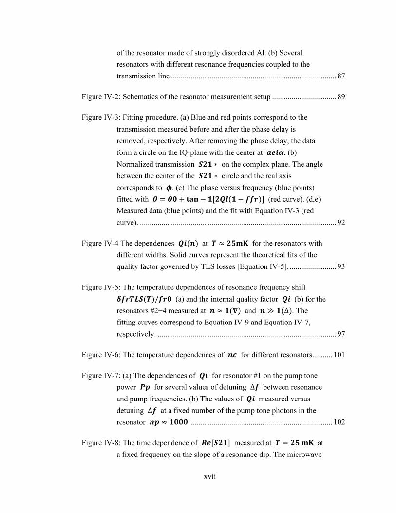
Figure IV-3: Fitting procedure. (a) Blue and red points correspond to the
transmission measured before and after the phase delay is
removed, respectively. After removing the phase delay, the data
form a circle on the IQ-plane with the center at . (b)
Normalized transmission ∗ on the complex plane. The angle
between the center of the ∗ circle and the real axis
corresponds to . (c) The phase versus frequency (blue points)
fitted with = + − [( − )] (red curve). (d,e)
Measured data (blue points) and the fit with Equation IV-3 (red
curve). ..................................................................................................... 92
Figure IV-4 The dependences () at ≈ for the resonators with
different widths. Solid curves represent the theoretical fits of the
quality factor governed by TLS losses [Equation IV-5]. ........................ 93
Figure IV-5: The temperature dependences of resonance frequency shift
()/ (a) and the internal quality factor (b) for the
resonators #2−4 measured at ≈ () and ≫ (∆). The
fitting curves correspond to Equation IV-9 and Equation IV-7,
respectively. ............................................................................................ 97
Figure IV-6: The temperature dependences of for different resonators. ......... 101
Figure IV-7: (a) The dependences of for resonator #1 on the pump tone
power for several values of detuning ∆ between resonance
and pump frequencies. (b) The values of measured versus
detuning ∆ at a fixed number of the pump tone photons in the
resonator ≈ . ......................................................................... 102
Figure IV-8: The time dependence of [] measured at = at
a fixed frequency on the slope of a resonance dip. The microwave

xviii
power corresponds to ≈ . Each point corresponds to the
data averaging over . .................................................................... 104
Figure IV-9: (a) The pulse sequence. (b) The time dependence of
measured at = . . The pump pulse at = +
was applied between = and = . . The pump
tone power corresponds to ¯ ≈ . Each data point was
averaged over 4000 cycles with the same readout delay time. The
inset shows CW measurement of versus with (red) and
without (blue) the pump signal and indicates the position of
used in the relaxation time measurement. The readout power was
at the single photon level for all measurements on this plot. ................ 107
Figure V-1: The tradeoff between the decay and dephasing protection in
superconducting qubits with a single charge or flux degree of
freedom. The band structure (top panels) and wavefunctions
(bottom panels) of a particle in quasiperiodic potentials: (a) the
free-particle regime and (b) the tight-binding regime. The
wavefunction overlap and the energy sensitivity ()/ do
not simultaneously vanish for any point (i). Flux (charge) qubits
correspond to the case in which the control parameter =
, kinetic energy = (), tunneling energy =
(), and |⟩ is a fluxon (charge) basis. .................................... 113
Figure V-2: (a) Simplified circuit scheme of the bifluxon qubit. Charging
energies of the superinductor and CPB are and ,
respectively. The qubit is controlled by the CPB charge and
the magnetic flux . (b) Optical image of the bifluxon qubit,
readout resonator, and the microwave transmission line. The inset
shows the SEM image of its central part: two JJs form the CPB
island (red false color), the long array of larger JJs acts as a
superinductor (blue), the narrow wire (green) forms the closed loop
and couples the qubit to the readout resonator. ..................................... 115
Figure V-3: Spectra of the bifluxon qubit: experimental data for the − |⟩
and − |⟩ transitions (symbols) and the result of exact
diagonalization of the circuit Hamiltonian in Eq. (1) (solid and
xix
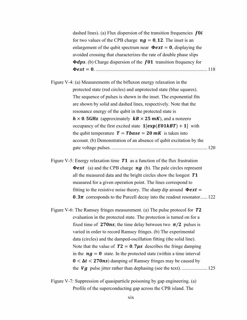
dashed lines). (a) Flux dispersion of the transition frequencies
for two values of the CPB charge = , . The inset is an
enlargement of the qubit spectrum near = , displaying the
avoided crossing that characterizes the rate of double phase slips
. (b) Charge dispersion of the transition frequency for
= . ............................................................................................ 118
Figure V-4: (a) Measurements of the bifluxon energy relaxation in the
protected state (red circles) and unprotected state (blue squares).
The sequence of pulses is shown in the inset. The exponential fits
are shown by solid and dashed lines, respectively. Note that the
resonance energy of the qubit in the protected state is
× . (approximately × ), and a nonzero
occupancy of the first excited state [() + ] with
the qubit temperature = = is taken into
account. (b) Demonstration of an absence of qubit excitation by the
gate voltage pulses. ............................................................................... 120
Figure V-5: Energy relaxation time as a function of the flux frustration
(a) and the CPB charge (b). The pale circles represent
all the measured data and the bright circles show the longest
measured for a given operation point. The lines correspond to
fitting to the resistive noise theory. The sharp dip around =
. corresponds to the Purcell decay into the readout resonator...... 122
Figure V-6: The Ramsey fringes measurement. (a) The pulse protocol for
evaluation in the protected state. The protection is turned on for a
fixed time of ; the time delay between two / pulses is
varied in order to record Ramsey fringes. (b) The experimental
data (circles) and the damped-oscillation fitting (the solid line).
Note that the value of = . describes the fringe damping
in the = state. In the protected state (within a time interval
< < ) damping of Ramsey fringes may be caused by
the pulse jitter rather than dephasing (see the text). ..................... 125
Figure V-7: Suppression of quasiparticle poisoning by gap engineering. (a)
Profile of the superconducting gap across the CPB island. The

xx
critical temperature of the thin CPB island is . ÷ . higher
than that in the thicker electrodes. (b)–(d) Spectroscopy of the
readout resonator as a function of for bifluxon qubits: without
gap modulation at (b), and with gap modulation at
(c) and (d). (e) The gap-engineered device at
. The dispersive shift of the readout resonator (color
coded) is measured at a fixed gate voltage over 9 hours. The
shift is converted into using the data of panel (c).
Abrupt jumps reflect the QP events ( = ±), gradual shift
corresponds to a monotonic drift of with a rate of less than
− per minute. .............................................................................. 127

1
CHAPTER I : INTRODUCTION
The superconducting artificial atoms [1, 2] have been an active experimental testbed for
quantum phenomena for more than three decades. As a non-dissipative circuit element
possessing a non-linear inductance, the Josephson junction has found numerous
applications ranging from quantum limited amplifiers [3] to the noisy intermediate-scale
quantum (NISQ) devices [4]. The most notable application in recent years was perhaps the
development of transmon qubits that combined sub-micron Josephson junctions with large
shunting capacitors [5]. Due to the simplicity and robustness of this design, the coherence
time of the transmon qubits has been increased up to 100 s, and the intermediate-scale
circuits comprising ~50 physical qubits have been developed [6].
Several challenges remain, however, for the state-of-art transmon devices. The
reported single- and two-qubit gate fidelities only marginally exceed the threshold for
implementation of the error correction code [7]. The large shunting capacitor, on the one
hand, makes transmon qubit insensitive to charge noise but, on the other hand, reduces the
qubit anharmonicity, and this imposes limitations on the speed of quantum gates [8, 9]. To
scale up the number of physical qubits while maintaining high fidelity, further
improvements of coherence are required.
2
It is currently believed that one of the main sources of decoherence is the two-level
defects, or Two-Level-Systems (TLSs), whose electric dipole moment fluctuates even at
ultra-low temperatures [10, 11]. Such defects usually reside in amorphous oxides that cover
surfaces of superconducting films and substrates. This issue is usually mitigated either by
improving the quality of all surfaces and interfaces in the process of fabrication [12] or by
reduction of qubit-TLSs coupling through proper design of the qubit Hamiltonian [13, 14].
Here, we pursue the second approach and focus on the component-level realization and
verification for protected circuits with preserved fluxon parity. This thesis is built on the
foundation laid out by a series of previous experimental efforts towards developing the
parity protected quantum circuits [15-17], and it reflects our recent work in this field [14,
18, 19].
To optimize the fluxon-parity protected circuit, it is necessary to better understand
the physics of low- Josephson junctions and superinductors based on such junctions.
The first four sections in this chapter review operation of low- superconducting
junctions, whereas in the following two sections we discuss superinductors and their
applications. We will close this chapter with two sections introducing the idea of protective
quantum circuits.

3
I.1 The Josephson phenomena and modeling of Josephson junctions
About five decades after superconductivity was discovered, in 1962, a theoretical
prediction was made by B. D. Josephson that when two pieces of superconductors were
brought in close vicinity and formed a weak link, a zero-voltage tunneling current could
flow through the weak link, or the junction. [20] According to Josephson, the non-
dissipative tunneling current is a non-linear function of the phase differences ≡ 2 −
1 between the phases of wavefunctions of Cooper pair condensates in the
superconducting electrodes:
= C
Equation I-1
The critical current C can be expressed as [21]
C,AB =
2ℎ
2
Equation I-2
where Δ is the superconducting energy gap, is the normal-state resistance of the
junction.
This current-phase non-linearity opens the possibility for using Josephson junction in
various applications including quantum-limited amplifiers and superconducting qubits.
When a current flowing through a junction exceeds the critical current, a non-zero average

4
voltage develops across the junction; this voltage is described by the second Josephson
relation [Equation I-3]:
=
2
Equation I-3
where Φ ≡ ℎ 2⁄ ≈ 20.6 Gμm
Taking into account the capacitance of a junction, , and active losses at high
frequencies, , the equivalent circuit representing the Josephson junction can be
schematically represented in Figure I-1.
Figure I-1: Symbolic circuit representation for a Josephson junction
This is so-called Resistive-and-Capacitive-Shunted-Junction (RCSJ) model of a
Josephson junction. By using the Kirchhoff's law for this circuit, we can write down the
total current as =
+
+ C sin . Or, using the Josephson relations, we can write
=
2
+
2
+ C
Equation I-4
This equation can be rewritten as

5
0 =
2
+
2
1
+ −
C
2 −
C
2
C + .
Equation I-5
This is the equation of motion for a particle with mass
moving in an effective
potential () =C
1 − −
C under a constant force
C
C. The term
represents damping in this system. By considering harmonic oscillations near
the minima of this so-called “washboard” potential, one can introduce the characteristic
frequency of these oscillations, the plasma frequency , and quality factor :
= 2
Φ
Equation I-6
= = 2
Φ ≡
Equation I-7
, where is the so-called Stewart-McCumber parameter[22]. The Stewart-McCumber
parameter and the quality factor have been used to distinguish between the
overdamped limit (, ≪ 1) and the underdamped limit (, ≫ 1) of the junction
dynamics.
The amplitude of the cosine term in the potential is the Josephson energy ≡C
;
the cosine function is tilted with the slope C⁄ , where is the DC current flowing
through the junction. This tilted cosine function (“the tilted washboard potential”) has been
6
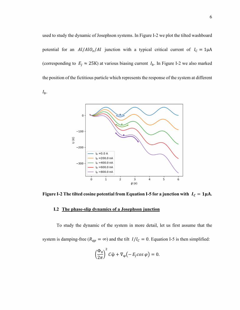
used to study the dynamic of Josephson systems. In Figure I-2 we plot the tilted washboard
potential for an // junction with a typical critical current of = 1μA
(corresponding to ≈ 25K) at various biasing current . In Figure I-2 we also marked
the position of the fictitious particle which represents the response of the system at different
.
Figure I-2 The tilted cosine potential from Equation I-5 for a junction with = .
I.2 The phase-slip dynamics of a Josephson junction
To study the dynamic of the system in more detail, let us first assume that the
system is damping-free ( = ∞) and the tilt / = 0. Equation I-5 is then simplified:
Φ
2
φ + ∇− = 0.

7
At the bottom of each well ≈ 2 and, by limiting deviations from the equilibrium
positions, we recover the harmonic oscillator equation
φ + = 0 with the
characteristic frequency =
. The energy difference between the adjacent
oscillator levels ℏ is
ℏ = 2
Equation I-8
where ≡()
is the charging energy associated with the capacitor in Figure I-1. In
Fig. I-3 we draw the first six energy levels for two values of while keeping fixed
[23].
Figure I-3: The potential and first six quantized energy levels (bands) for junctions
with different charging energy.
As we can see in Figure I-3, the energy ratio ⁄ determines whether the system should
be treated classically or quantum mechanically. When ⁄ is large, the ground state

8
wavefunction is localized near the potential minima. With decreasing ⁄ , the
wavefunctions become delocalized over many potential minima due to tunneling.
The non-zero probability of tunneling between adjacent minima of the washboard potential
results in generation of the so-called phase slip, an abrupt 2 change of a phase difference
across the junction and generation of the voltage pulse () such that ∫ ()dt = Φ/2.
The phase slips due to tunneling are known as the quantum phase slips (QPS), they are
characterized by the rate ≈
ℏexp −
.
ℏ [24, 25] where Δ =
8(1 − ⁄ ) and attempt frequency ≈ . However, the phase slips can also
occur due to the over-the-barrier thermal activation at non-zero temperatures. The rate of
the thermally activated phase slips (TAPS) depends exponentially on the temperature:
≈ ⁄ [24, 26]. Figure I-4 schematically shows the phase dynamics
corresponding to the QPS and TASP. At zero tilt, the phase slips with different signs of the
phase change occur with the same probability and, as a result, the average voltage across
the junction is zero. However, when the junction is biased with current , the non-zero tilt
breaks the symmetry and a non-zero average voltage proportional to the phase slip rate is
generated across the junction. The dynamics of the system in this case depends on
dissipation. In the underdamped regime the energy gained by a system in the process of
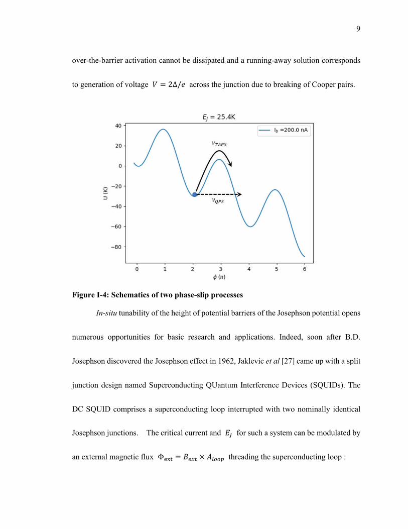
9
over-the-barrier activation cannot be dissipated and a running-away solution corresponds
to generation of voltage = 2Δ/ across the junction due to breaking of Cooper pairs.
Figure I-4: Schematics of two phase-slip processes
In-situ tunability of the height of potential barriers of the Josephson potential opens
numerous opportunities for basic research and applications. Indeed, soon after B.D.
Josephson discovered the Josephson effect in 1962, Jaklevic et al [27] came up with a split
junction design named Superconducting QUantum Interference Devices (SQUIDs). The
DC SQUID comprises a superconducting loop interrupted with two nominally identical
Josephson junctions. The critical current and for such a system can be modulated by
an external magnetic flux Φ = × threading the superconducting loop :

10
= |cos(Φ Φ⁄ )|
Equation I-9
We will utilize the SQUIDs geometry in this work to investigate the dynamics of phase
slips in the junction as a function of magnetic flux Φ and temperature .
I.3 The current-voltage characteristics of a Josephson junction
Upon increasing the biasing current and exceeding the critical current , the
non-zero voltage is generated across the junction, which corresponds to “sliding” of a
fictitious mass along the tilted washboard potential. When is reduced, in case of low
dissipation the potential tilt needs to be reduced to nearly zero in order to re-trap the
fictitious particle. A more rigorous calculation can be done for an underdamped junction
as shown in [28]: drops to zero only when becomes less than the retrapping current
≈
. The Q dependence of indicates that the system can be returned to zero
voltage state if only the energy gained from the biasing tilt (as phase advances by 2 from
one potential well to the next one) is dissipated through damping, Q. On the other hand,
in heavily damped junctions (~1) dissipation dominates inertia, and we expect no
hysteresis in the IVC. This corresponds to the case where the fictitious particle slowly
slides down the inclined washboard potential.

11
We illustrate the above scenarios in Figure I-5. In both cases the characteristic scale of
currents is provided by the critical current C,AB. The Ambegaokar - Baratoff relation
Equation I-2 allows us to relate C,AB to the normal-state resistance N , one of important
fabrication parameters.
Figure I-5: The IVCs for junctions with different levels of dissipation. Left: Q>1 Right:
Q<1
Due to non-linear IV characteristics, the Josephson-junction-based elements were
considered attractive for digital applications [29-31]. In these applications, the
underdamped junctions were driven between superconducting and resistive IVC branches
to realize digital zeros and ones. These devices featured ultrafast operation (2 × 10 J/
bit at 770 GHz, [32]) and extremely low energy consumption. They operated in the
“classical” Josephson regimes ≫ , in order to avoid phase slips and maintain
12
the hysteresis in the IVc. Typical parameters are ≈ 2500K and ≈ 4.5mK for
2μm × 2μm niobium junctions which operate at ≈ 4 in the RSFQ circuits [33].
However, due to the requirement of helium refrigeration for operation of these devices and
rapid progress of CMOS industry, superconducting logics found rather limited applications.
With the advancement of superconducting artificial atoms and dilution refrigeration
in the late 1990s Josephson junctions regained attention as non-linear and low-dissipative
elements of superconducting qubits. The Cooper pair box (a small superconducting island
flanked by two JJs) became one of the first solid-state quantum bit (qubit) experimentally
realized in 1998 [34]. Soon after, various superconducting qubits archetypes were
implemented [35] by mapping the logical quantum states to different physical realizations.
The fluxonium qubit, for example [36], is based on a junction with 10 ≳ ⁄ ≳ 1 and
≫ , where is the inductance energy for the superinductor element which will be
addressed below. The latter requirement can be satisfied if the superinductor with
inductance energy = (Φ 2⁄ ) ⁄ has a sufficiently large . Similarly, in the case of
bifluxon [14] it is also required that ≫ to decouple the qubit from flux noises.
Experimentally, tuning of can be achieved either by changing the oxidation parameters
or by varying the junction area (Equation I-2). In this thesis, the low- junctions with
≈ 0.01 ÷ 10K and ≈ 0.001 ÷ 1K have been fabricated by e-beam lithography.

13
Besides and , another characteristic energy scale is provided by the
temperature. Nominally, the base temperature for a standard cryogen-free dilution
refrigerator is around ≈ 0.01 ÷ 0.02K with cooling power in sub-mW range. Any
poor thermal anchoring between sample carrier or wirings to the cold plate could result in
higher sample temperatures which would increase the rate of TAPS process. Depending on
how small is, the temperature could be the dominant parameter that controls
dissipation in the circuit.
I.4 The phase diffusion regime in underdamped junctions
As was discussed in the previous section, the thermally activated phase slips could
harm the performance of low- junctions by driving the system into a resistive state. The
detailed analysis of the effect of non-zero temperature in the underdamped junctions was
provided by Kivioja et. al,[24]. By considering the quality factor at plasma frequency,
, and the energy dissipated between adjacent potential maxima Δ ≈ 8 ⁄ ,
Kivioja et. al showed that the maximum possible power dissipated due to phase diffusion
before switching to a state with ≈ 2∆/ can be expressed as
2
Φ×
Δ
2= ×

14
where = 4 ⁄ is the maximum possible current carried by underdamped junctions
in the Phase Diffusion (UPD) regime. At < , there is non-zero probability for a
fictitious particle to be retrapped after escape from a local minimum. As a result, instead
of a running-away state with = 2Δ ⁄ , the IVC demonstrates a non-zero slope at
< . Such frequency dependent quality factor was also used to explain the IVCs for
underdamped junctions where both hysteresis feature and non-zero have been observed
[37]. The value of therefore provide valuable information regarding the nature of
damping in the junction circuits, and in Chapter III we will use the zero-bias resistance as
one of the main characteristics of low- junctions. The summary of different regimes
considered in [24] is shown in Fig.I-7.
Figure I-6: (Left) Different regimes for an underdamped junction with small
(dashed lines at 60 nA, 130 nA and 200 nA, respectively). The corresponding
indicate the temperatures above which the junction enters the UDP regime. The
vertical red line separates the QPS regime from the TAPS which takes place at the
crossover temperature . (Right) Comparison of the UDP dynamics with the
dynamics shown in Figure I-4. (Inset) Equivalent circuit of the junction with
frequency dependent dissipation. Image was adopted from [24].

15
In this work, we will investigate the regimes of low-frequency transport in low-
underdamped junctions with ≥ ≫ . Two experimental observables, and ,
will be used to classify and characterize the low- junctions used in our quantum circuits.
These results will be presented in Chapter III.
I.5 Kinetic inductance
In the following two sections, we turn our attention to the second components in
the bifluxon circuit, the superinductor, which is a dissipationless element with microwave
impedance greatly exceeding the resistance quantum =
(). In classical linear circuits
an inductor is usually realized as a wound thin wire with an inductance being proportional
to the wire’s length. Such an element unavoidably has a large parasitic capacitance which
drastically reduces the high-frequency impedance of the inductor. As a quantitative
example, consider two parallel wires of radius and distance apart, one end of the
wires is short-circuited. Such device can be modelled as a transmission line where its
specific inductance and specific capacitance can be calculated as = log( ⁄ ) ⁄ and
= log( ⁄ )⁄ , respectively. Even though it is possible to scale up the inductance by
increasing the length of the wire, the impedance remains logarithmically small =
⁄ =
( ⁄ )
. As a result, the inductor has a relatively low cutoff frequency ;

16
above this frequency the circuit response is dominated by parasitic capacitance and the
device no longer works as an inductor. Clever designs and advanced micro-fabrication
techniques, as demonstrated in [38], can still realize the device impedance ≈ 30Ω
greater than R at microwave frequencies, but such device requires a 100μm × 100μm
footprint and sophisticated removal of bulk substrate to reduce the dielectric constant and
minimize the parasitic capacitance. It would be very desirable to find an alternative
candidate for superinductors with a much smaller footprint and less complicated fabrication
methods.
The alternatives do exist, and they are based on the kinetic inductance rather than
on the geometric one. According to the Drude model, the current in a conductor with carrier
density and cross-sectional area under an AC electric field = exp() can be
expressed as
= =
1
1 +
where is the momentum relaxation time. As frequency increases such that ≫ 1,
the response per unit length becomes inductive with
=
2
1
Equation I-10

17
However, this inductance, which is associated with inertia of charge carriers, is usually
masked by dissipation in a normal metal at frequencies lower than
, which is usually in
the THz range. On the other hand, in superconductors due to the zero loss at low
frequencies, one can exploit this inductance at ≪ . Since the energy in such inductors
is stored in the kinetic energy of the Cooper pair condensate with density (Equation
I-10) rather than in the magnetic field, such an inductance is called the “kinetic inductance”.
High kinetic inductance has been reported for several strongly disordered materials
including [39, 40], [41], [42, 43], and granular aluminum ( )[44].
Such materials have been found applications in magnetometers [45] and single-photon
detectors [46].
Still challenges exist for implementing the disordered thin films in the quantum
circuit as SIs. One common use of inductors in quantum circuits is the microwave
resonators for the qubit readout. These resonators have typically a sub-mm length and a
sub- μm width. In order to have predictable specifications and performance, it is required
that the film should have high uniformity at this relatively large length. It is not trivial to
develop the deposition technique that would guarantee uniformity for highly resistive films
approaching the superconductor-insulator transition [47]. Thorough optimization of
18
fabrication processes is required to achieve reproducibility of disordered nanowire
fabrication.
Before we end the discussion for superinductors and make a final remark, let us
briefly review another approach which was also commonly employed. This approach is
based on the use of kinetic inductance of Josephson junctions, with its own pros and cons
which we will address in the next section.
I.6 The non-linear inductance of a Josephson junction
Blessed of being non-linear and non-dissipative simultaneously, the Josephson
junction is also a promising candidate for realizing the SI. The junction non-linearity has
found many applications ranging from Josephson metamaterials [48], superinductors [15,
49, 50], quantum-limited amplifiers [3, 51] to various artificial atoms developed in the
superconducting qubits family [14, 16, 52, 53]. Most of these applications rely on the non-
linear inductance associated with the Josephson current-phase relation Equation I-1,
Equation I-3. Let us rewrite the relations as
= cos ,
2
Φ =
we then have
×
=
cos , and from the definition of inductance =
one expects that the inductance for the Josephson junction can be expressed as:
19
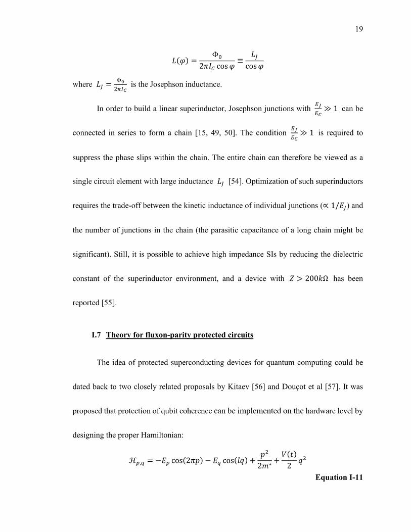
() =Φ
2 cos ≡
cos
where =
is the Josephson inductance.
In order to build a linear superinductor, Josephson junctions with
≫ 1 can be
connected in series to form a chain [15, 49, 50]. The condition
≫ 1 is required to
suppress the phase slips within the chain. The entire chain can therefore be viewed as a
single circuit element with large inductance [54]. Optimization of such superinductors
requires the trade-off between the kinetic inductance of individual junctions (∝ 1/) and
the number of junctions in the chain (the parasitic capacitance of a long chain might be
significant). Still, it is possible to achieve high impedance SIs by reducing the dielectric
constant of the superinductor environment, and a device with > 200Ω has been
reported [55].
I.7 Theory for fluxon-parity protected circuits
The idea of protected superconducting devices for quantum computing could be
dated back to two closely related proposals by Kitaev [56] and Douçot et al [57]. It was
proposed that protection of qubit coherence can be implemented on the hardware level by
designing the proper Hamiltonian:
ℋ, = − cos(2) − cos() +
2∗+
()
2
Equation I-11

20
When () ≪ 1 and ∗ ≫ 1, the ground state of the first three terms corresponds to
a linear combination of the wavefunctions denoted as |⟩ and localized around the
minima of potential at = 2 ⁄ , where and are integers. From the
exponential shift theorem, the effect of cos(2) = + 2⁄ operator in the
first term can be viewed as a shift in the -coordinate by ±2 , which maps |⟩ to
(| + ⟩ + | − ⟩) 2⁄ . As a result, with sufficiently small () the full Hamiltonian ℋ,
projected onto the low-energy subspace becomes
ℋ, = −1
2( + ) +
1
2()(2 ⁄ )
where is the shift operator and |⟩ = | + ⟩ . In the absence of perturbation
() = 0, the ground state wavefunction is -periodic in with -fold degeneracy for
the ground states: Ψ = ∑ |⟩ , = . Such degeneracy decouples the
Hamiltonian from environmental noises in the -space, hence it justified the name “parity
protection”. More advanced fault tolerant gate operations can be achieved with a fast pulse
of () [58]. The parity protection together with fault tolerant gate controls forms a
protective computation scheme for the artificial atoms.
In superconducting artificial atoms, the Josephson Hamiltonian is 2-periodic in
its phase coordinate. It is possible to reconstruct Equation I-11 by utilizing -periodic
Josephson elements (the so-called Josephson rhombi) based on the Aharonov-Bohm effect
21
[16] or 4-periodic Josephson elements based on the Aharonov-Casher effect [17]. In this
work we will be focusing on the realization of components for the latter circuit
implementing the 4-periodicity of Josephson energy.
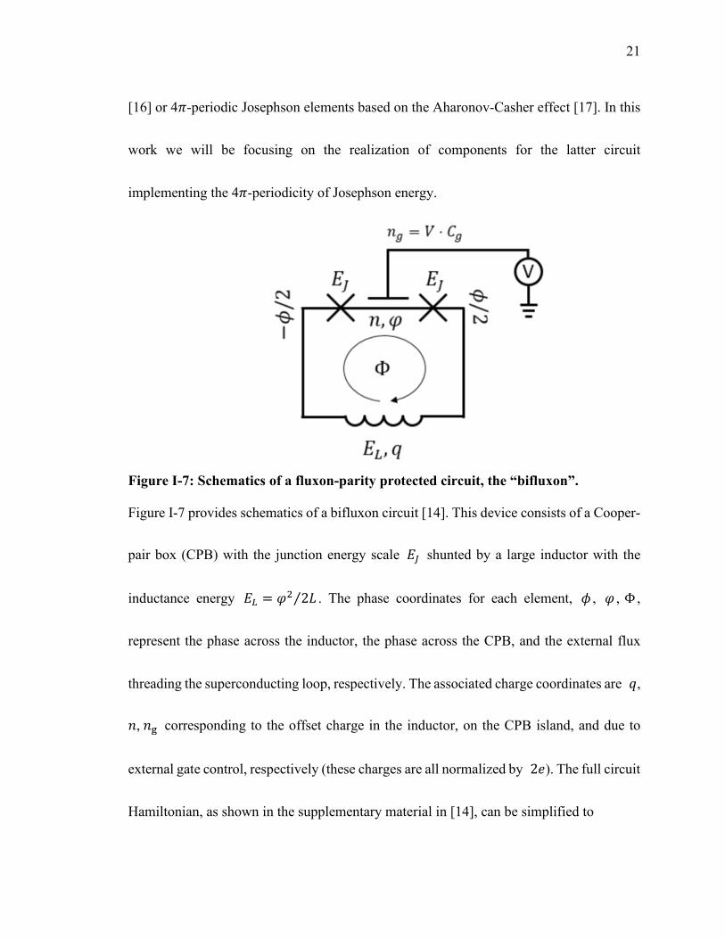
Figure I-7: Schematics of a fluxon-parity protected circuit, the “bifluxon”.
Figure I-7 provides schematics of a bifluxon circuit [14]. This device consists of a Cooper-
pair box (CPB) with the junction energy scale shunted by a large inductor with the
inductance energy = 2⁄ . The phase coordinates for each element, , , Φ ,
represent the phase across the inductor, the phase across the CPB, and the external flux
threading the superconducting loop, respectively. The associated charge coordinates are ,
, corresponding to the offset charge in the inductor, on the CPB island, and due to
external gate control, respectively (these charges are all normalized by 2). The full circuit
Hamiltonian, as shown in the supplementary material in [14], can be simplified to

22
ℋ± = −4 − ±(),
±() = ± cos( 2⁄ ) +
2 − 2
Φ
Φ
The coordinates [, ], [, ] ∝ are the conjugated pairs [, ] = as in Equation
I-11. Here, the ground state energy in was localized around the minimum near =
2 where is an even or odd integer (2 or 2 + 1) for or , which gives rise
to the aforementioned degeneracy and parity protection for the bifluxon circuit. The
wavefunction can be expressed as Ψ ≈ ( − ) exp− ⁄ 4⁄ and is
associated with a fluxon excitation |2⟩ or |2 + 1⟩.
I.8 Components for fluxon-parity protected circuits
The experimental realization of a bifluxon qubit relies on two factors. Firstly, the
fluxon excitation picture requires level quantization of bound states in the inductor phase
coordinate , which implies the depth of potential wells to be greater but not much
greater than the level spacing ℏ at zero temperature ≳ ℏ . In particular this
requires an accurate characterization of relevant energy scales such as and physical
temperature to correctly describe phase slips phenomena in low- junctions. This
provides motivation for the study of such junctions at ultra-low temperatures.

23
The second requirement is the realization of a superinductor, which we introduced
briefly in section I.5. The SI as a circuit element must satisfy two conditions. Firstly, it
should be non-dissipative over a wide frequency range. Secondly, it should demonstrate
sufficiently small parasitic capacitance such that = ⁄ > , where ≡
ℎ (2)⁄ ≈ 6.5kΩ. The purpose of such superinductor in a bifluxon circuit is to minimize
decoherence induced by the flux noise [14]. The qubit sensitivity to a decoherence
process can be estimated by the amplitude of the charge and flux dispersion of the transition
energy Φ, ,
= Φ = 0, = 0.5 − Φ = π, = 0.5
= Φ = π, = 0 − Φ = π, = 0.5
It has been shown in [14] that a minimized dispersion can be achieved when ⁄ is
sufficiently large and, at the same time, remains small. An exponentially small flux
dispersion can be achieved in the regime where 2 ≪ ℏ exp−2 ⁄ .
24
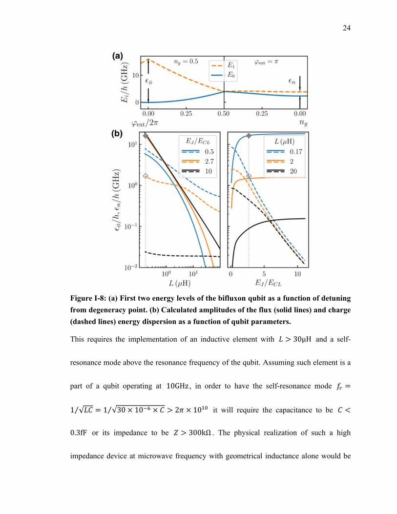
Figure I-8: (a) First two energy levels of the bifluxon qubit as a function of detuning
from degeneracy point. (b) Calculated amplitudes of the flux (solid lines) and charge
(dashed lines) energy dispersion as a function of qubit parameters.
This requires the implementation of an inductive element with > 30μH and a self-
resonance mode above the resonance frequency of the qubit. Assuming such element is a
part of a qubit operating at 10GHz , in order to have the self-resonance mode =
1 √⁄ = 1 √30 × 10 × ⁄ > 2 × 10 it will require the capacitance to be <
0.3fF or its impedance to be > 300kΩ . The physical realization of such a high
impedance device at microwave frequency with geometrical inductance alone would be

25
impossible, but it can be achieved by using suspended JJ chains [55] or disordered
superconducting nanowires [18, 40, 59].
To implement the fluxon-parity protective scheme, it is therefore necessary to better
understand the ultra-low-temperature characteristics of low- junctions and
superinductors. This is the main focus of this thesis.
I.9 Thesis overview
In this chapter, we briefly reviewed the theoretical background and characteristics
of the elements comprising the bifluxon qubit. Two critical elements, the low- junctions
and a non-dissipative high impedance superinductor, were introduced. In this chapter we
discussed the principles of operation of these elements, their realization will be addressed
in the following chapters. Common methodology used in this work, including nano-
fabrications and DC and MW characterization, will be described in Chapter II. A complete
list of devices studied in this work can also be found at the end of that chapter. In Chapter
III, we characterize the low- junction by reviewing the transport data in DC
measurement for a chain of SQUIDs. By varying the Josephson energy with external
flux, we studied the effect of phase slips in such junctions at ultra-low temperatures. In
Chapter IV we investigate the kinetic inductance of disordered superconducting thin

26
films by fabricating coplanar waveguide resonators. This chapter was adopted from [18].
The works in Chapter V is adopted from the experimental section in [14], which
demonstrates a bifluxon circuit that consist of CPB and the superinductors made from the
Josephson junction chains. In Chapter VI we conclude this thesis by formulating the main
findings and providing an outlook for the future experiments with the bifluxon circuits.
27
METHODOLOGY
In this chapter, we focus on the methods of preparation and characterization of Josephson
junctions and disordered films used in this work. As a book-keeping section, the
methodology unavoidably include many details and become extensive. However, to
benefits the future junior researchers, I will still try to put down comprehensive notes in
this chapter. Modularized process steps will be introduced in the first section, while the
measurement protocols are detailed in the second section.
II.1 Fabrication
Nanofabrication is no doubt one of the fields that require sophisticated training and
experiences in an artisanal setting such as university laboratories. Depending on the scales
of the lab and funding, it is not uncommon that PhD students are the backbone of process
integration and equipment maintenance work force after thorough trainings. Being the
foundation of major discoveries of contemporary electronics, nanofabrication plays a
crucial role as a first step in the study of our quantum circuit. Indeed, nanofabrication is
challenging not only because of our limited understanding of physics behind the scenes in
the uncharted nanoscale realms, but also how robust and repeatable our processes should
be to provide reliable devices with nominally-the-same characteristics from run to run. One
28
common practice in nowadays semiconductor foundries is setting up detail process flow
tables together with the inspection handbook, in order to achieve reproducibility from
devices to devices and between different operators. In this work we follow similar ideas to
maintain our fabrication parameters in project specific flows to keep track of all process
changes. Here in this section, we will first introduce our key process modules with the
corresponding tools and inspection criteria, and then we proceed with the process flows for
different devices in this work.
The processes involved throughout the work are modularized into two sub-groups:
lithography and film formation. By combining above modules to form a process layer for
a specific circuit element such as a junction, meander, or capacitor, we can study the
devices connected to various electromagnetic environments.
II.1-1 Lithography
Let us begin with the lithography module. In this work the lithography works are
performed using the NPGS/SEM ebeam writing bundle with FEI Sirion XL30 30keV
SEM from Thermal Fisher Scientific. After a user defines the layout for a specific project
in DesignCAD 2000 LT, a runfile containing the pattern information and sequential
instructions is assembled in the Nanometer Pattern Generation System (NPGS) maintained
29
by Dr. Joe Nabity under Windows XP. Typically, two types of instructions, beam
movement and beam dosage, are generated in the NPGS and sent to different part of the
ebeam control PC. The NPGS system will translate and send the pre-defined movement
commands to a local computer to control the beam movements, and then convert the beam
dosage to the electric signal dwell time on a beam blanker (Scanservice model 880) based
on the ratio between the nominal dosage and the beam current user provided in the runfile
before beginning of each process. The alignment between beam blanker, aperture, and
condensing coil is essential to the optimum ebeam writing and maximized beam current
outputs; it is in general recommended to perform the vacuum bakeout and full
mechanical/software alignments on annual basis.
Although the recent advancement in ebeam writer enables reproducible -scale
patterning, high uniformity of such pattern across a device such as long chains of junctions
remains challenging in a laboratory setting. For designs involved in this work such as
junction chains requiring reproducible junction areas across a sub-millimeter size window,
longer working distance and rather small aperture size (size 4, 30μm in diameter) are used
to maximize the depth of focus to accommodate the differences in heights across the chip.
The typical beam size is about 5 − 10nm while the maximum field of view is 1mm.
For devices larger than the field of view we stitched several write windows and verified

30
the stitching results through a series of stitching markers. To ensure the uniform thermal
distribution during the preparation of ebeam-resist, the chip was prebaked on the surface
of a thick copper slab heated by the hotplate and monitored with a standalone thermometer.
All lithography parameters are finetuned based on the specific pattern density and are
recorded in the process flow tables listed at the end of this section. We would like to point
out that a shortened baking time is adopted during the resist pre-bake step in order to
minimize the thermal budgets applied to junctions in the case that another lithography layer
is required after junction formation. Because of that, it is necessary to pay extra attention
to the development condition such as the MIBK solution temperature to stay consistent
between batches. The solution temperature was monitored at 23 ± 0.5 by a K-type
thermal couple.
The junctions in this work are fabricated by the Manhattan pattern technique with
angle evaporation and differential development in bilayer e-beam resists, and the details
can be found in chapter 3 in [60]. The in-situ oxidation process performed between
deposition of the bottom and top aluminum electrodes is tuned to produce the required
value of . Typically we used the dry Oxygen partial pressure 1 − 100 torr and
oxidized the structures for 5 − 15 minutes. With optimization of this process in our lab,
the standard deviations for the normal state resistance for a nominally sub-μm-wide
31
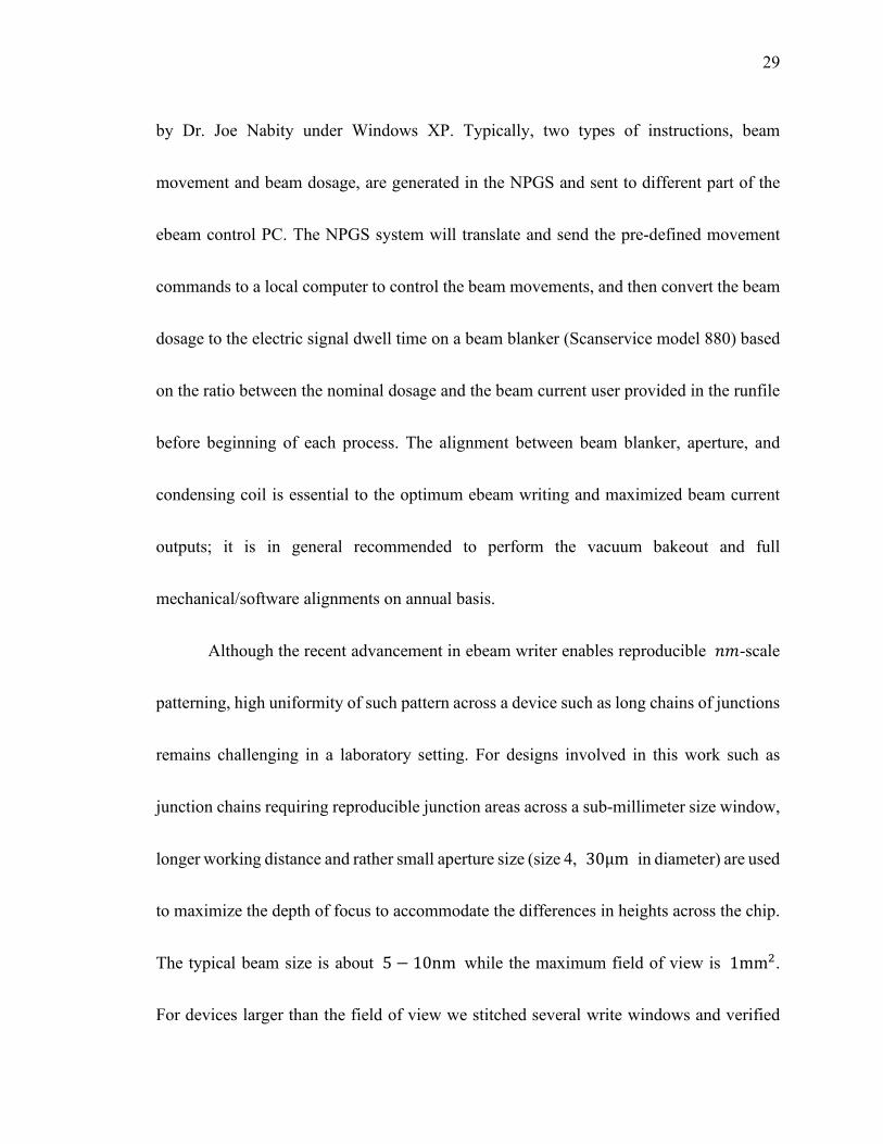
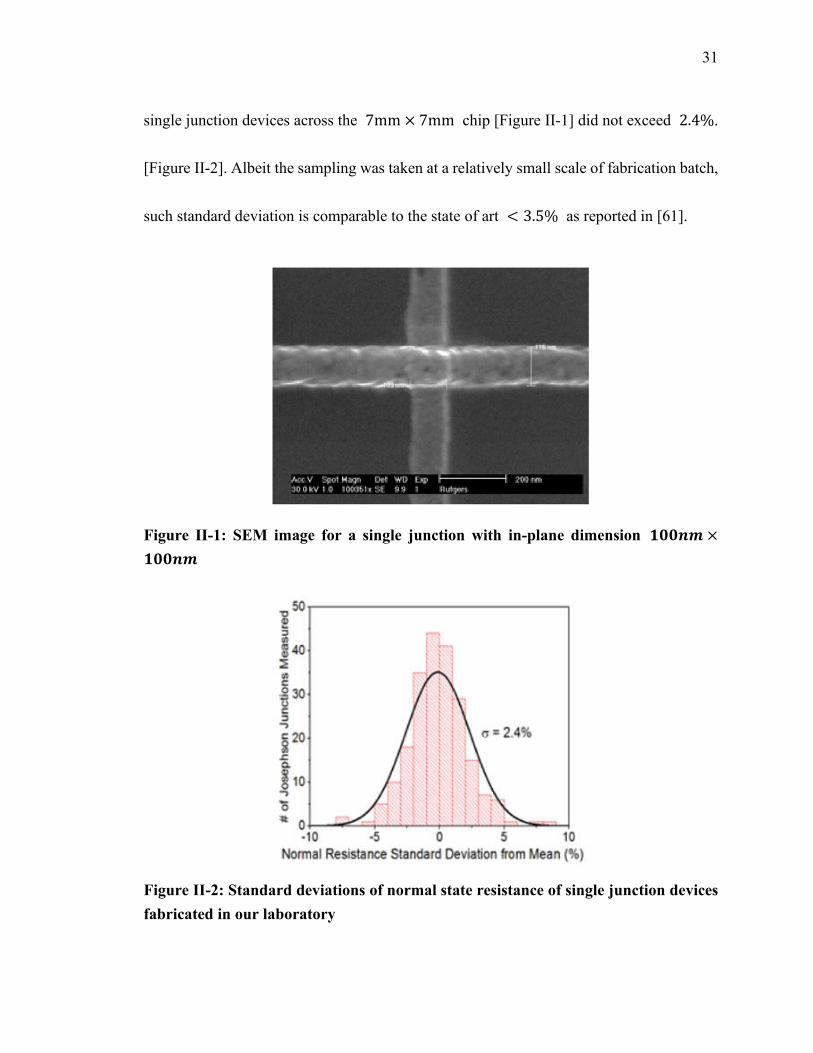
single junction devices across the 7mm × 7mm chip [Figure II-1] did not exceed 2.4%.
[Figure II-2]. Albeit the sampling was taken at a relatively small scale of fabrication batch,
such standard deviation is comparable to the state of art < 3.5% as reported in [61].
Figure II-1: SEM image for a single junction with in-plane dimension ×
Figure II-2: Standard deviations of normal state resistance of single junction devices
fabricated in our laboratory

32
For junction array devices with an overall sub-millimeter length, however, the
standard deviation of junction areas across the chain went up to 40% with this lithography
recipe before further fine-tuning (blue histogram in Figure II-3). This was mostly due to
shorter working distances used in fabrication of the single junction devices, which resulted
in a smaller depth of focus and therefore greater in-plane variations. By increasing working
distance from 8mm to 15mm, we reduced the junction area variation to less than 10%
across a 200μm-long chain (orange histogram in Figure II-3).
Figure II-3: Scattering of the junction areas in the chain devices. The data in
blue/orange histograms are before/after the process optimization.

33
Small scattering in and are crucial for proper operation of our SQUID
based circuit: minimizing deviations from the nominal values of and is important
for realizing the maximum superinductance in the junction-based superinductors where
simultaneously frustration of all SQUID unit cells is required. In this work we typically
observe a 90%-reduction of critical current for the SQUID structure at the magnetic field
corresponding to full frustration Φ = Φ/2, where Φ is the magnetic flux through the
SQUID loop.
II.1-2 Film deposition and junction fabrication
Three project-specific process modules are included in this section: uniform
junction oxidation during ebeam evaporation, ion milling integration, and granular
aluminum AC sputtering. Other standard process parameters can be found in the process
flow tables listed at the end of the fabrication section.
Junction fabrication
The junction oxidation non-uniformity has been a major bottleneck in developing
junction technologies for decades. Although aluminum films form robust and pin-free
tunneling barriers, the barrier transparency is extremely sensitive to residual moisture
presented in the chamber or oxygen source. In this work a liquid nitrogen cold trap was

34
inserted between the sample space and oxygen source tank to remove the potential moisture
before entering the chamber, and the chamber was evacuated down to < 5 × 10 torr
before oxygen was introduced for oxidation.
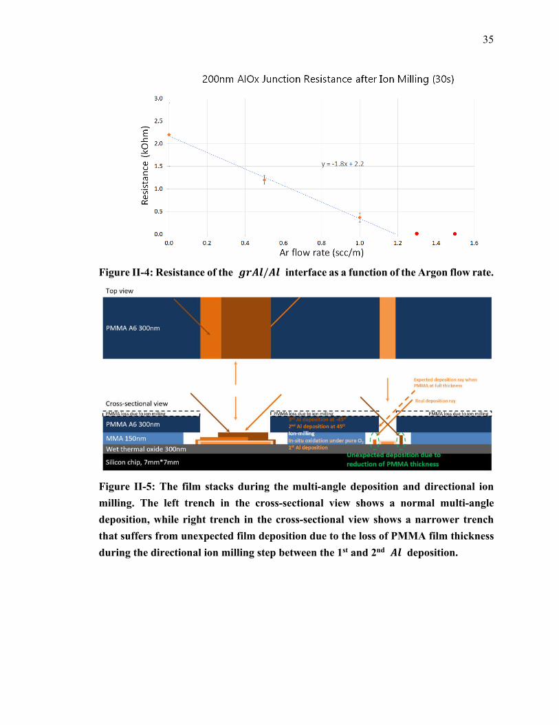
Ion milling for hybrid device integration
To integrate superconducting elements fabricated in different chambers and ensure
good superconducting contact between different layers, we used the 10mm DC cathode
KRI Argon ion source for in-situ ion milling of the film surface before deposition of top
layers. One common issue in the process of -ion milling of aluminum oxide with
PMMA mask is weak selectivity of milling. We were able to perform deeper etching by
dividing a long etching run into several short etching sequences to allow the PMMA cool
down between individual steps. In this work the milling recipe was tested by measuring
the critical current of the resulting joint and ensuring that this current is two to three order
of magnitude greater than the critical current of all junctions in the devices (Figure II-4).
The removal rate of baked PMMA is ~3A/s at acceleration voltage 90V, and this should
be taken into account in the design of the junction fabricated by multi-angle deposition to
avoid unexpected film deposited into the undercut as shown in Figure II-5.
35
Figure II-4: Resistance of the / interface as a function of the Argon flow rate.
Figure II-5: The film stacks during the multi-angle deposition and directional ion
milling. The left trench in the cross-sectional view shows a normal multi-angle
deposition, while right trench in the cross-sectional view shows a narrower trench
that suffers from unexpected film deposition due to the loss of PMMA film thickness
during the directional ion milling step between the 1st and 2nd deposition.
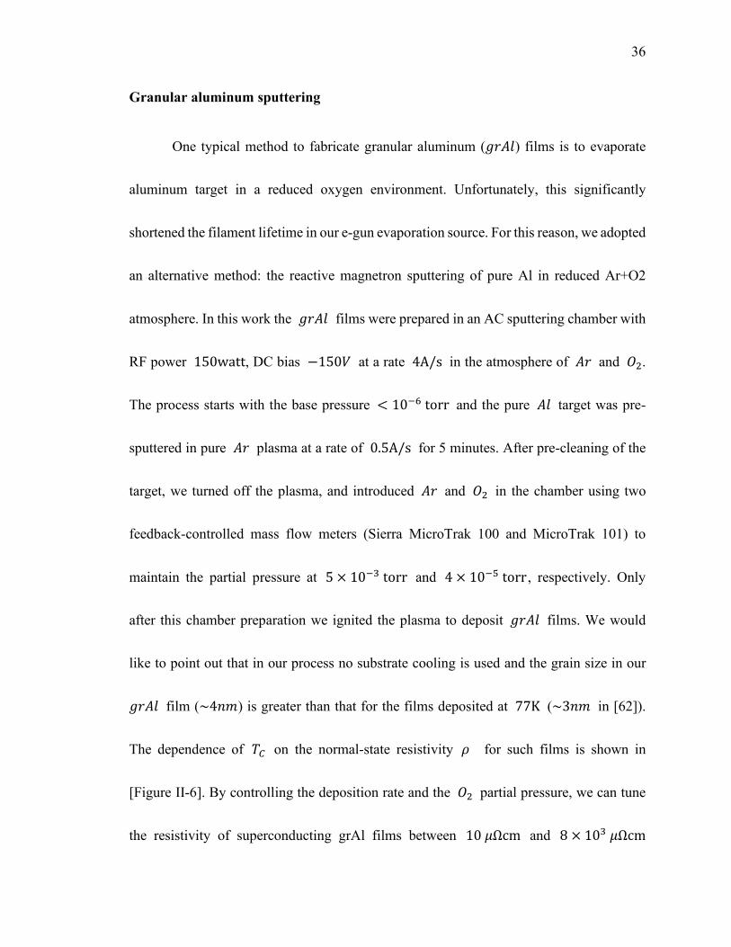
36
Granular aluminum sputtering
One typical method to fabricate granular aluminum () films is to evaporate
aluminum target in a reduced oxygen environment. Unfortunately, this significantly
shortened the filament lifetime in our e-gun evaporation source. For this reason, we adopted
an alternative method: the reactive magnetron sputtering of pure Al in reduced Ar+O2
atmosphere. In this work the films were prepared in an AC sputtering chamber with
RF power 150watt, DC bias −150 at a rate 4A/s in the atmosphere of and .
The process starts with the base pressure < 10 torr and the pure target was pre-
sputtered in pure plasma at a rate of 0.5A/s for 5 minutes. After pre-cleaning of the
target, we turned off the plasma, and introduced and in the chamber using two
feedback-controlled mass flow meters (Sierra MicroTrak 100 and MicroTrak 101) to
maintain the partial pressure at 5 × 10 torr and 4 × 10 torr, respectively. Only
after this chamber preparation we ignited the plasma to deposit films. We would
like to point out that in our process no substrate cooling is used and the grain size in our
film (~4) is greater than that for the films deposited at 77K (~3 in [62]).
The dependence of on the normal-state resistivity for such films is shown in
[Figure II-6]. By controlling the deposition rate and the partial pressure, we can tune
the resistivity of superconducting grAl films between 10 Ωcm and 8 × 10 Ωcm

37
(Figure II-8) which provides the sheet kinetic inductance in a range between 2.5 fH sq⁄ to
2 nH sq⁄ for 40nm thick films. The films are then patterned into various geometries with
nanolithography. Figure II-7 shows one of such structures - a meandered nanowire with
sub-μm width and few thousands of squares total, which provides the kinetic inductances
up to a few μH.
Figure II-6: The − “dome” for granular aluminum deposited in this work. The
dashed curve corresponds to the literature data for grAl films deposited at 77K.

38
Figure II-7: A meandered nanowire made of granular aluminum. The device is false
colored for clarity. The rest of the structure, which was not in a galvanic contact with
the device, was fabricated in order to reduce the nonuniformity of the nanowire width
due to the proximity effect in the process of e-beam nanolithography.
Figure II-8: The sheet resistance of films as a function of the flow.

39
II.1-3 Process flows
Figure II-9: Process flow for junction chain project

40

41
Figure II-10: Process flow of microwave resonator project

42
II.2 Measurement
II.2-1 DC measurement
All experiments presented in this work were performed using a BlueFors SD250
dilution refrigerator rated 250 μW at 100 mK and the base temperature around 25 mK.
The detailed working principle of dilution refrigeration could be found in previous thesis
works from our lab, for example chapter 3 and 4 in [63]. The external magnetic field used
in this work was same order of magnitude as Earth’s magnetic field, and to reduce stray
magnetic fields the entire cryostat is enclosed with a customized μ-metal shield which
enabled attenuation of the Earth’s field by two orders of magnitude. Two customized sets
of wiring and instrument modules labeled as DC and MW have been developed and
installed in the cryostat.
The wiring for DC setup inside the cryostat consists of 12 twisted pairs made of
resistive alloys : (5: 1) with multiple thermal anchoring points to isolate the
sample from room temperature and to reduce the thermal loads as shown in Figure II-11.
Near the cold finger which supported the sample holder, twisted pairs are carefully winded
on an Oxygen-Free Copper (OFC) tubing filled with copper-powder epoxy (Figure II-12
left), which serves as a cryogenic lowpass filter and a final thermal anchoring point before
connecting to the sample holder. On the detachable sample holder, 100kΩ surface mount
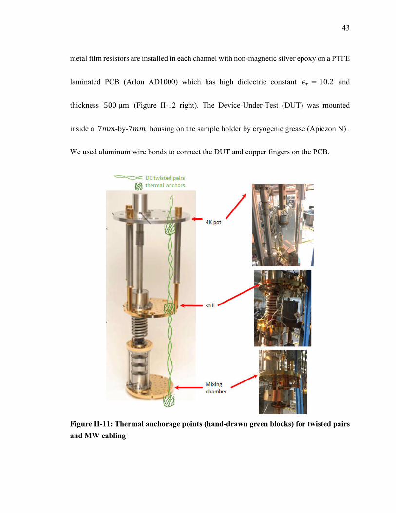
43
metal film resistors are installed in each channel with non-magnetic silver epoxy on a PTFE
laminated PCB (Arlon AD1000) which has high dielectric constant = 10.2 and
thickness 500 μm (Figure II-12 right). The Device-Under-Test (DUT) was mounted
inside a 7-by-7 housing on the sample holder by cryogenic grease (Apiezon N) .
We used aluminum wire bonds to connect the DUT and copper fingers on the PCB.
Figure II-11: Thermal anchorage points (hand-drawn green blocks) for twisted pairs
and MW cabling
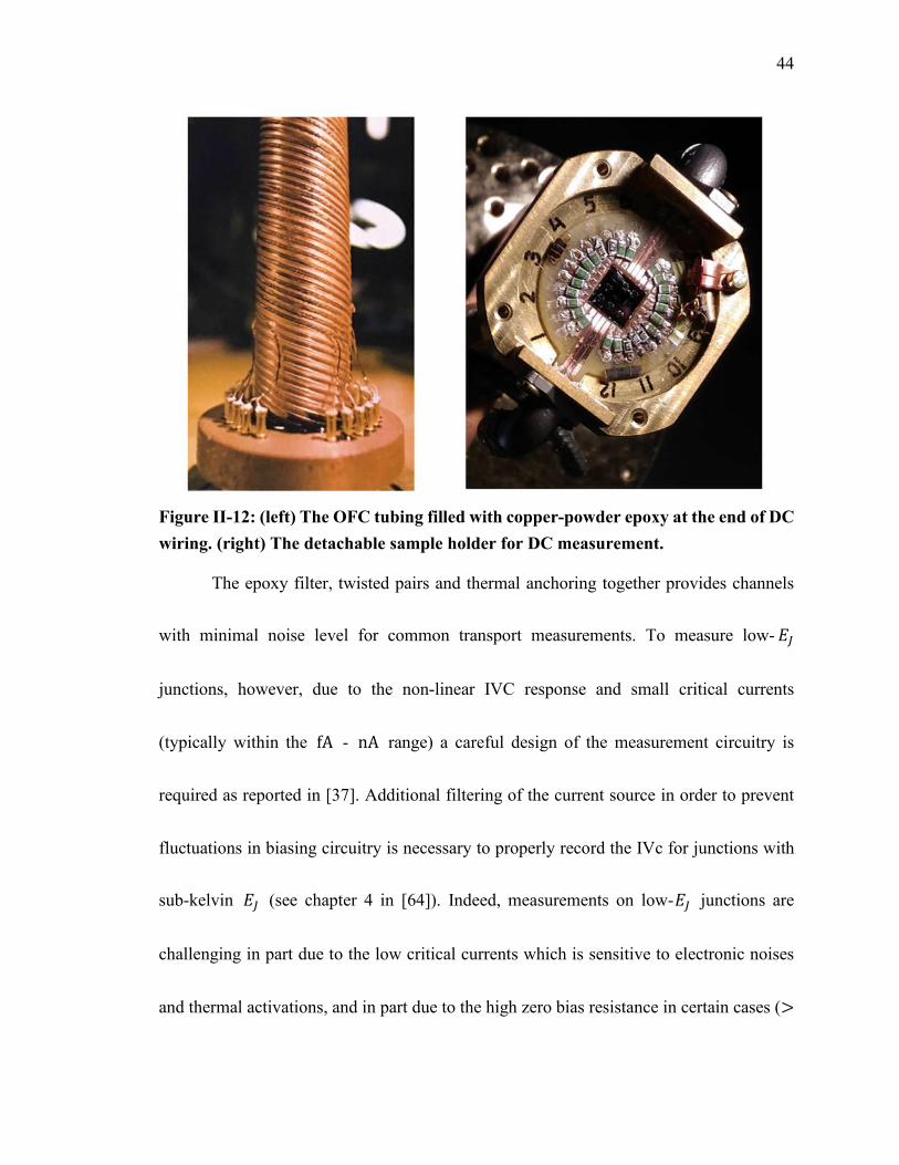
44
Figure II-12: (left) The OFC tubing filled with copper-powder epoxy at the end of DC
wiring. (right) The detachable sample holder for DC measurement.
The epoxy filter, twisted pairs and thermal anchoring together provides channels
with minimal noise level for common transport measurements. To measure low-
junctions, however, due to the non-linear IVC response and small critical currents
(typically within the fA - nA range) a careful design of the measurement circuitry is
required as reported in [37]. Additional filtering of the current source in order to prevent
fluctuations in biasing circuitry is necessary to properly record the IVc for junctions with
sub-kelvin (see chapter 4 in [64]). Indeed, measurements on low- junctions are
challenging in part due to the low critical currents which is sensitive to electronic noises
and thermal activations, and in part due to the high zero bias resistance in certain cases (>

45
20MΩ as reported in [65], for example). In this work we try to mitigate the first concern
by installing cascaded low pass filters at the source end and tackle the second concern by
employing a voltage preamplifier (DL Instrument 1201) with input impedance as high as
few GΩ when being DC-coupled. The comparison of filtering effects on the IVcs will be
elaborated in section III.1.
The wiring and instrument schematic outside of the fridge is shown in Figure II-13
and Figure II-14 for current and voltage biasing schemes, respectively. A commercial LC
low pass filter (BLP 1.9+, DC − 1.9MHz) and a homemade RC filter (DC − 8Hz) box with
variable biasing resistors up to 1GΩ are inserted between the source Tektronix AFG3252
(or Keithley 6200) and DUT. Two types of biasing boxes are made and used depends on
the biasing schemes. The voltage drops across DUT are amplified with a voltage preamp
DL1201 and measured by HP 34401A digital multimeter with PC automation scripts such
as LabVIEW and Python module QCoDeS.
Figure II-13 The wiring schematics for DC current source measurements

46
Figure II-14 The wiring schematics for DC voltage source measurements
As a final remark before we turn our attention to MW setup, in this work we
characterized the parasitic capacitances with AH 2500A capacitance bridge (Andeen-
Hagerling). Indeed, it is difficult to directly measure the parasitic, but still we managed to
estimate the value by extending the wiring stage by stage. Here the results are attached for
future references (Figure II-15).
Figure II-15: Characterizing the parasitic capacitance
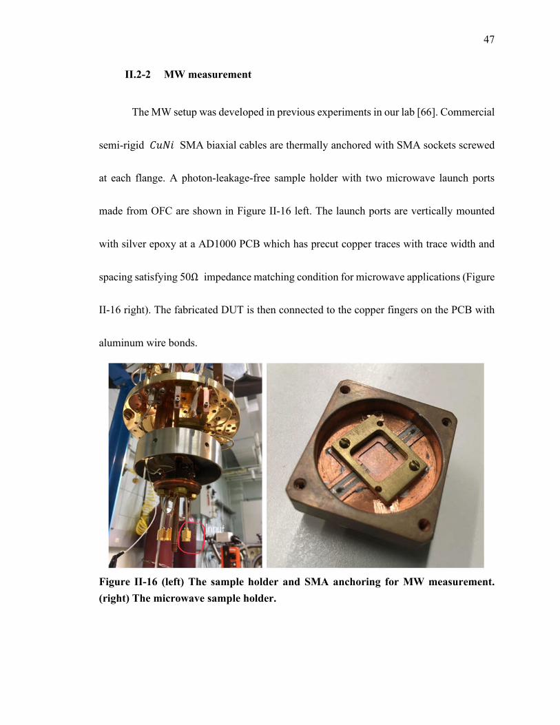
47
II.2-2 MW measurement
The MW setup was developed in previous experiments in our lab [66]. Commercial
semi-rigid SMA biaxial cables are thermally anchored with SMA sockets screwed
at each flange. A photon-leakage-free sample holder with two microwave launch ports
made from OFC are shown in Figure II-16 left. The launch ports are vertically mounted
with silver epoxy at a AD1000 PCB which has precut copper traces with trace width and
spacing satisfying 50Ω impedance matching condition for microwave applications (Figure
II-16 right). The fabricated DUT is then connected to the copper fingers on the PCB with
aluminum wire bonds.
Figure II-16 (left) The sample holder and SMA anchoring for MW measurement.
(right) The microwave sample holder.
48
With this setup (Figure II-17) we have performed the transmission measurement
over a wide range of MW power including testing of the MW resonators in the single-
photon population regime. The probe signal at and the pump signal at , generated by
two microwave synthesizers, were coupled to the input of the cryostat through directional
couplers. Depending on the experiment performed, the pump signal could be pulsed using
an internal RF switch of the microwave synthesizer. Attenuators and low-pass filters were
installed in the microwave input line to prevent leakage of thermal radiation into the
resonator. The signal, after passing the sample, was amplified by a cryogenic high-electron
mobility transistor (HEMT amplifier Caltech CITCRYO 1-12, 35 dB gain between 1 ÷
12 GHz) and two 30dB room-temperature amplifier. Two cryogenic Pamtech isolators
(each provides 18dB isolation between 3 ÷ 12 GHz ) were anchored at the base
temperature to reduce the 5K noise from the HEMT amplifier. The amplified signal was
downconverted to the intermediate frequency (IF) = | − | ≈ 30MHz using mixer
M1 with the local oscillator signal . The IF signal was digitized using the card
AlazarTech ATS 9870 at 1GS/s. The magnitude and phase of the signal was obtained
by digital demodulation as
= ⟨() (2)⟩ + ⟨() (2)⟩
= (⟨() (2)⟩ ⟨() (2)⟩⁄ )
Equation II-1
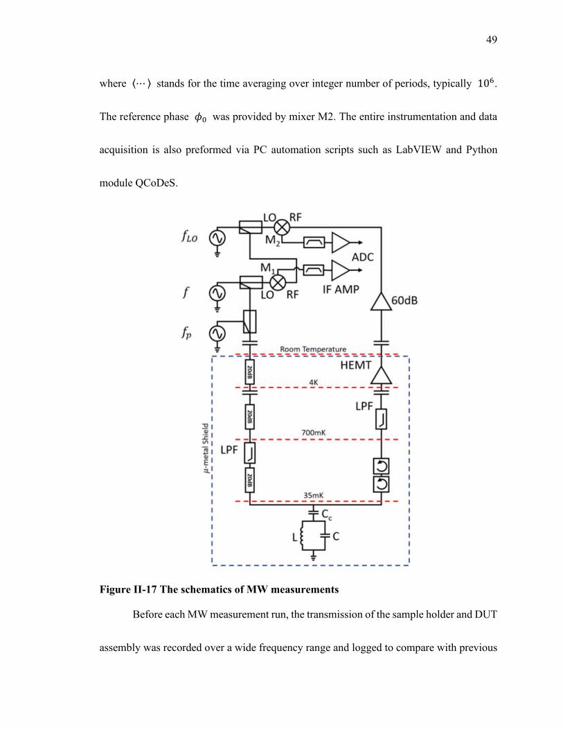
49
where ⟨⋯ ⟩ stands for the time averaging over integer number of periods, typically 10.
The reference phase was provided by mixer M2. The entire instrumentation and data
acquisition is also preformed via PC automation scripts such as LabVIEW and Python
module QCoDeS.
Figure II-17 The schematics of MW measurements
Before each MW measurement run, the transmission of the sample holder and DUT
assembly was recorded over a wide frequency range and logged to compare with previous

50
measurements. The purpose of such comparison is to ensure no spurious resonances or
losses exist in the entire MW setup due to material fatigue or loose connections (Figure
II-18).
Figure II-18: Transmission background check before each cool down
II.2-3 Temperature control and magnetic fields characterization using
SQUID geometry
To closely monitor the temperature of the DUT a thin film NTC
thermometer was attached to the sample holder, and three brass braids directly connected
the holder to the coldplate for enhanced thermal anchoring. At the cryogenic temperature,
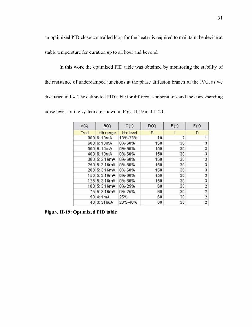
51
an optimized PID close-controlled loop for the heater is required to maintain the device at
stable temperature for duration up to an hour and beyond.
In this work the optimized PID table was obtained by monitoring the stability of
the resistance of underdamped junctions at the phase diffusion branch of the IVC, as we
discussed in I.4. The calibrated PID table for different temperatures and the corresponding
noise level for the system are shown in Figs. II-19 and II-20.
Figure II-19: Optimized PID table

52
Figure II-20: Optimized noise level and thermal fluctuation at different temperatures.

53
Taking advantage of the periodicity of the cosine dependence of () in
Equation I-9, we can also monitor the performance of our superconducting magnet. This
periodicity of the resistance of a SQUID biased at > is shown in Figure II-21.
Figure II-21 Periodic response of a SQUID to external magnetic field.

54
We did observe flux focusing effects for different designs with different metal density.
Flux focusing is due to flux repulsion from nearby superconducting pads, it results in an
increase of the magnetic field in the SQUID loop (Figure II-22). In Figure II-23 we listed
design variants as we used in this work.
Figure II-22: Comparison of the magnet currents that correspond to = for
three designs with different area of the SQUID loop.
Figure II-23: Various designs of SQUID used in this work.

55
II.3 Lists of samples
II.3-1 Low- junctions
Below we listed low- devices we studied in Chapter III.
Figure II-24: in , in are the normal state resistance and the area
of single junction in the chain. , in are the single junction Josephson
energy ≡ C ⁄ and charging energy ≡ ⁄ , respectively. ,,
in are the single junction critical current predicted from Equation I-2 and the
switching current that experimentally measured. shows how many SQUIDs
are in series in the design. . indicates the source of capacitor shunting the
junction where “” means external capacitor was fabricated, “ ” means the
junction has intrinsically large area parallel plate capacitors to provide low , and
“ ” represents data point that are measured before external capacitor was
fabricated. Finally, and ; in are the zero-biased resistance at zero B-
field and B-field at full frustration point, respectively.

56
II.3-2 Resonators with superinductance
Below we listed four resonators in Chapter IV designed with different , and .
II.3-3 Bifluxon devices
In Chapter V we demonstrate a prototype bifluxon circuit, and here we list the parameters
for each component (SI and CPB) in the circuit.
With the reliable and consistent methodologies ranging from fabrication, measurement, to
experimental control knobs such as temperature and magnetic fields, we are ready to move
on to the investigation and realization of the circuit elements for bifluxon qubits.

57
THERMAL EFFECTS IN LOW- JOSEPHSON JUNCTIONS
Josephson junctions with the Josephson energy less than 0.5 have already been
employed as non-linear elements of superconducting qubits [36]. Though of these
junctions remains much greater than the physical temperature of qubits (10 ÷ 50), a
non-zero rate of thermally activated phase slips in these junctions might limit the qubit
coherence. Indeed, the coherence time of superconducting qubits approaches 1 [67],
and even rare events at such a time scale might become significant.
In the past strong experimental and theoretical effort was aimed at better
understanding of a crossover from the classical Josephson behavior (well-defined phase
difference, very large quantum fluctuations of charge) to the Coulomb-blockade regime
(localized charges, very large quantum fluctuations of phase). This crossover is commonly
attributed to the decrease of the parameter /. The coherent phase slip processes (the
so-called quantum phase slips, or QPS), whose rate exponentially increases with
approaching / ≈ 1, do not contribute to dissipation, though they might affect the
dephasing time in qubits.
In this thesis we are mostly concerned with a different regime Δ ≫ ≥ ≫ ,
which is more relevant to operation of protected superconducting circuits. In order to
explore the dynamics of low- junctions at ultra-low temperatures, we designed JJs with
58
a very low transparency of the tunneling oxide and the values of Josephson energy
between 0.1 ÷ 10. The charging energy =()
of these junctions remained below
10 due to shunting the junctions with external capacitors. This chapter reviews the
results of the low-frequency transport measurements with these structures.
III.1 Sample design
All the samples studied in this Chapter have been implemented as SQUIDs, in order
to be able to in-situ tune by applying the external magnetic field. Figure III-1
schematically shows the design of a chain of SQUIDs formed by small junctions
(0.2 × 0.2 ). The area of the SQUID loop varied between 6.8 and 49. Our
experiments were focused on the JJs with 1 > ≫ : this regime is relevant to the
quantum circuits in which JJs are shunted with large external capacitors (such as the
transmon qubit). Large / ratio would also significantly reduce the rate of quantum
phase slips ∝ −2
[68]. Typical specific capacitance of the junction tunneling
barrier is about 50 fF/ , and in order to reduce down to 20 the
junctions should either have relatively large in-plane dimensions ( > 4 ) or be
shunted with external capacitors ( > 200fF). We have used both methods in different
structures (Figure III-1). In the external capacitors approach, several designs of the
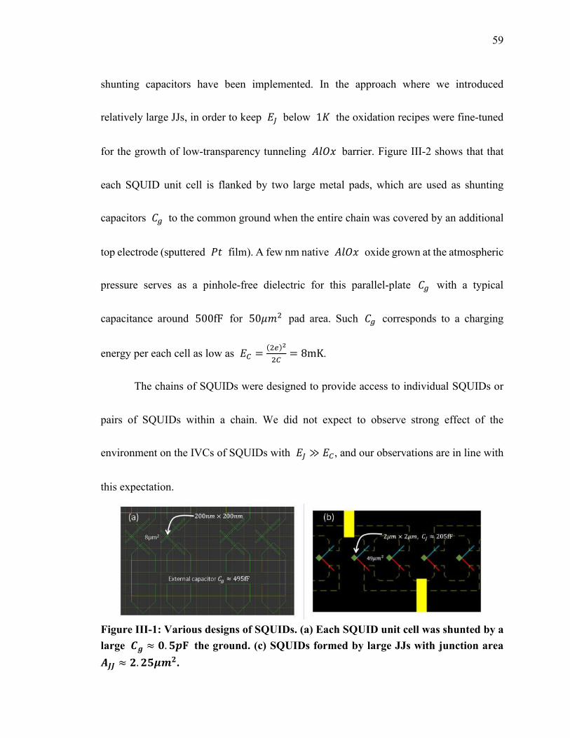
59
shunting capacitors have been implemented. In the approach where we introduced
relatively large JJs, in order to keep below 1 the oxidation recipes were fine-tuned
for the growth of low-transparency tunneling barrier. Figure III-2 shows that that
each SQUID unit cell is flanked by two large metal pads, which are used as shunting
capacitors to the common ground when the entire chain was covered by an additional
top electrode (sputtered film). A few nm native oxide grown at the atmospheric
pressure serves as a pinhole-free dielectric for this parallel-plate with a typical
capacitance around 500fF for 50 pad area. Such corresponds to a charging
energy per each cell as low as =()
= 8mK.
The chains of SQUIDs were designed to provide access to individual SQUIDs or
pairs of SQUIDs within a chain. We did not expect to observe strong effect of the
environment on the IVCs of SQUIDs with ≫ , and our observations are in line with
this expectation.
Figure III-1: Various designs of SQUIDs. (a) Each SQUID unit cell was shunted by a
large ≈ . the ground. (c) SQUIDs formed by large JJs with junction area
≈ . .

60
Figure III-2: Device schematics and the circuit diagram for devices with shunting
capacitors and a common ground (opaque blue pad).
III.1 Noise reduction in the measurement setup.
The noise reduction was our primary concern in characterization of low-
junctions. Most of our measurements have been performed in the constant current mode.
The value of the critical current at = 0 for an // JJ with = 1 is
, = 30 according to the Ambegaokar-Baratoff formula (Equation I-2). With
further reduction of and proliferation of phase slips at elevated temperatures , the
current range well below 1 becomes relevant.
Figure III-3 illustrates the importance of proper filtering of noises in both the
current supply part and the voltage recording part of the measuring setup. By using the

61
combination of cascaded low-pass filters and 100 resistors on the sample holder, we
were able to record switching currents in the range (Figure III-3).
Figure III-3: The IVCs recorded for a two-unit SQUID device with different
measurement set-ups at = (sample D059B0N1 in Table III-1). Each
SQUID unit consisted of two nominally identical junctions with an area
. × . and resistance 10kΩ ( = . ). Due to a large shunting
capacitor to the ground, this device has ⁄ = ⁄ ≫ . Without
thorough filtering, the IVC was smeared and the IVC hysteresis, expected for an
underdamped junction at low , was significantly reduced. Filtering of all leads used
for the IVC measuring restores the critical current which is close to , , and
enables observation of a well-developed hysteresis. The inset shows that the noise level
in our measurements is around . .
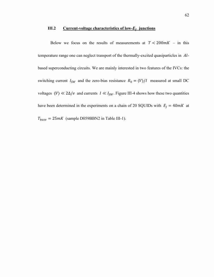
62
III.2 Current-voltage characteristics of low- junctions
Below we focus on the results of measurements at < 200 – in this
temperature range one can neglect transport of the thermally-excited quasiparticles in -
based superconducting circuits. We are mainly interested in two features of the IVCs: the
switching current and the zero-bias resistance = ⟨⟩/ measured at small DC
voltages ⟨⟩ ≪ 2∆/ and currents ≪ . Figure III-4 shows how these two quantities
have been determined in the experiments on a chain of 20 SQUIDs with = 40 at
= 25 (sample D059BBN2 in Table III-1).

63
Figure III-4: (left) The current-voltage characteristic (IVCs) for a chain of 20 SQUIDs
with = (sample D059BBN2 in Table III-1). (right) The enlargement of the
region of small currents/voltages. Note that the resistance is non-zero for all biasing
currents. As soon as the biasing current exceeds = . (indicated by a cyan
arrow), the voltage across the chain rapidly increases, and at even greater currents
approaches the value × ∆/, where is the number of SQUIDs and ∆ is the
sum of superconducting energy gaps in the electrodes that form a junction. At ≥
× ∆/ dissipation is due to generation of non-equilibrium quasiparticles. At <
the non-zero resistance ≈ is due to thermally activated phase
diffusion (section I.4). Note that for such low- junctions, the switching current is
three orders of magnitude smaller than the Ambegaokar-Baratoff critical current
, ≈ . .
For convenience, below we separately discuss the data for junctions with ≈ 1
and ultra-low- junctions.
III.3 Josephson junctions with ≈
In the regime ≫ , and < 200 one may expect to observe the
“classical” behavior of Josephson junctions: ≈ , and a well-developed IVC
hysteresis typical for underdamped junctions with the McCumber parameter ≫ 1
(section I.3 and [22]). Indeed, in zero magnetic field, the IVCs shown in Figure II-5 meet

64
these expectations. The value of = 18 is close to , = 32, and, within the
accuracy of our measurements ≈ 10 ÷ 10 , depending on the magnitude of , we
could not detect a non-zero .
Figure III-5: IVCs of two connected in series SQUIDs with = . at =
(blue curve) and = . (red curve) at base temperature (sample D059B0N1 in
Table III-1).
At full frustration Φ = 0.5Φ where we expect to be minimized (Equation
I-9), this device demonstrated behavior that resembled the Coulomb-blockade regime (red
curve in Figure II-5). Note that for most of the studied samples in this regime is of an
order of the base temperature. The zero-bias resistance at full frustration (Φ =
0.5Φ, ) becomes strongly dependent on temperature at > 0.2 (Figure III-6) where
the concentration of thermally generated quasiparticles becomes significant. The drop of
with temperature at > 0.25 (Figure III-6) can be approximated by the Arrhenius
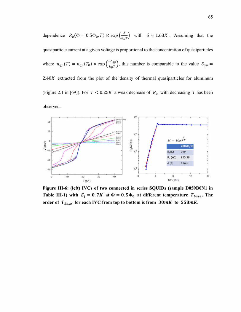
65
dependence (Φ = 0.5Φ, ) ∝
with ≈ 1.63 . Assuming that the
quasiparticle current at a given voltage is proportional to the concentration of quasiparticles
where () = () × exp
, this number is comparable to the value =
2.40 extracted from the plot of the density of thermal quasiparticles for aluminum
(Figure 2.1 in [69]). For < 0.25 a weak decrease of with decreasing has been
observed.
Figure III-6: (left) IVCs of two connected in series SQUIDs (sample D059B0N1 in
Table III-1) with = . at = . at different temperature . The
order of for each IVC from top to bottom is from to .

66
Figure III-7: (a) IVCs of a single SQUID with = . (sample D079N6 in Table
III-1) measured at different magnetic fields (we only marked four selected curves for
clarity). A sub-gap voltage plateau at ≈ appears at > . . (b) The
dependence of on the superconducting solenoid biasing current. (c) The
measured ()/( = ) as a function of (/) . The dash line
corresponds to the dependence ∝
. The reason for observed
deviations from the dash line for
< . remains unclear.
Even in the “classical” regime ≫ , we obtained several unexpected results.
Firstly, we noticed that the dependence of (Φ) for some samples could significantly
deviate from the expected dependence (Φ) = (Φ = 0) × cos (Φ/Φ) in the B-

67
fields approaching the full frustration cos
≈ 0 (Figure III-7). Secondly, we have
observed sub-gap ( < 2∆/) voltage steps on the IVCs (Figure III-7 a), which
significantly reduced the accuracy of extraction of and close to full frustration.
We speculated that one reason for appearance of sub-gap steps might be the Fiske
resonances [70, 71]. However, we could not identify the circuit elements that would be
responsible for the corresponding resonance frequencies at = (75μeV) ℎ⁄ ≈ 18GHz
(for the silicon substrate this frequency corresponds to a length scale ≈ 5). This issue
requires further investigation.
As we will discuss below, for the devices with ( = 0) < 1 further deviations
from the “classical” Josephson behavior have been observed. With decreasing ,
rapidly drops well below the , value (it becomes several orders of magnitude smaller
than , for devices with ≈ 0.1), and dramatic increase of the zero-bias resistance
is observed.
III.4 Josephson junction ≈ . and the effect of shunting JJ with
As it was expected, we observed the charging effects in the low- JJs without
external capacitive shunts. Figure III-8 shows the IVC for a chain of 30 SQUIDs based on
JJs with resistance = 40Ω and = 0.17K. The IVCs have been measured for the
68
same device before and after the deposition of top capacitor pad. This top electrode,
being isolated from the rest of the circuit by the native oxide, significantly increased
the capacitance connected in parallel with individual SQUIDs (from 2 fF to 500 fF) and
decreased from 1.5K to 8mK (
from 0.13 to 25 before and after Pt deposition,
respectively).
Deposition of the electrode did not significantly affect the IVCs at voltages
> × 2∆ - the normal state resistance of the chain decreased by about 2.5% after an
additional lithographic cycle and deposition, from 610Ω to 595Ω. However, the
IVCs have been significantly modified at low currents/voltages: the lower inset in Figure
III-8 shows that Pt deposition significantly increased , up to 20 pA and reduced the
zero-bias resistance R . We attribute these findings to suppression of the charging
effects and associated with them quantum phase slips with the rate ∝
exp−2 ⁄ by an increase of the shunting capacitance.
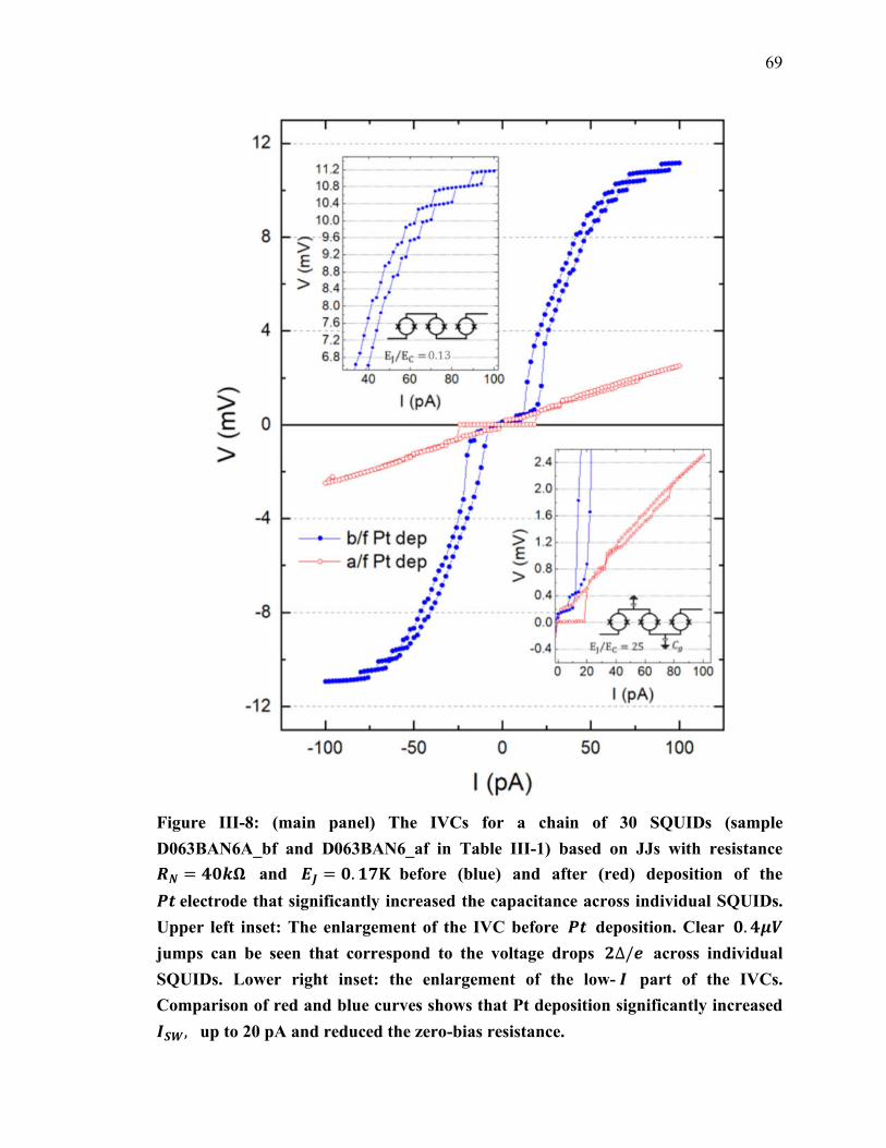
69
Figure III-8: (main panel) The IVCs for a chain of 30 SQUIDs (sample
D063BAN6A_bf and D063BAN6_af in Table III-1) based on JJs with resistance
= and = . before (blue) and after (red) deposition of the
electrode that significantly increased the capacitance across individual SQUIDs.
Upper left inset: The enlargement of the IVC before deposition. Clear .
jumps can be seen that correspond to the voltage drops ∆/ across individual
SQUIDs. Lower right inset: the enlargement of the low- part of the IVCs.
Comparison of red and blue curves shows that Pt deposition significantly increased
, up to 20 pA and reduced the zero-bias resistance.

70
III.5 Discussion: the suppressed switching currents
In this section we include all our junction devices in the regime ≪ ≤ and
provide brief discussions for the suppressed switching currents and potential source
of dissipation.
It is expected that the main source of dissipation in the regime ≪ ≤ ≪ ∆
is a relatively high rate of incoherent thermally activated phase slips (TAPS). The DC
transport in the regime ≪ has been theoretically considered by Ivanchenko and
Zilberman [72] (the “IZ theory”). This theory considers a stochastic noise V() as a
driving force for switching the underdamped junctions in the resistive state. The equation
of motion for a classical Josephson junction (Equation I-4) can be rewritten as:
+ ()
=
2
+
2
+ C
By solving the corresponding Fokker-Planck equation, the DC Josephson current
( = V + V) can be parameterized by the ratio of the potential energy Ω and the
noise fluctuation (Θ) , ≡ Ω ⁄ where Ω = 2eIR ℏ⁄ and D = ΘR(2 ℏ⁄ ) . Note
that the source of noise fluctuations can be either thermal Johnson-Nyquist noise [73] or
electronic noises, and in the analysis all noises appear as an emf, (k ⁄ , , … ).
The resulting IVCs obtained in [72] are shown in Figure III-9. At z = 2 a sharp turn
around 10 × ⁄ ≈ 5 indicates a decrease of switching current from , to

71
0.02, when the noise level increased from Θ ≪ Ω to Θ = 0.5Ω, and an increase of a
zero-bias resistance .
.
Figure III-9: Analytical solutions from [72] for IVCs at different fluctuation level ≡
⁄ . At = a sharp turn was observed around × ⁄ ≈ , indicating a
decrease of switching current from to . when the noise level increased
from ≪ to = . .
The IZ theory predicts that ∝ at small [74]. In Figure III-10, we
plotted the predictions of according to the IZ theory for = 20. This
noise corresponds to the Johnson-Nyquist noise = 4Δ generated at =
50 by the 100 resistors connected in series with the device in Figure II-13. The
bandwidth was estimated as Δ ≈ 2⁄ , where 2⁄ = 0.5 ÷ 5GHz is the range of
plasma frequency of the shunted JJs.

72
Figure III-10: The switching current measured for different devices at ≈
and the magnetic field increasing from = to B corresponding to
= /. The red dash-dotted line corresponds to the switching current predicted
by the IZ theory in presence of = .
Most of the data points in Figure III-10 are 1-2 orders of magnitude smaller
than predicted by the IZ theory. A possible explanation for this discrepancy might be
more complex phase dynamics in the devices with a very high TAPS rate, outside of the
limits of applicability of the IZ theory. Another possibility is an exponentially strong

73
sensitivity of the TAPS rate to the noise level in the setup and the physical temperature of
a device, the parameters that are not easy to control in all experiments.
Figure III-10 also included the data for five devices where we tuned
(Equation I-9) by varying the external magnetic flux threading the SQUIDs loop. The
effective for these devices was calculated as = 2 cos 2
. By tuning
over an order of magnitude, we observed rather complicated dependences that
varied between and .

74
Figure III-11: The zero-biased resistance measured for different devices at ≈
and the magnetic field increasing from = to B corresponding to
= /. The red dash-dotted line corresponds to predicted by the IZ theory
in presence of = .
The zero-bias resistance in Figure III-11 follows a similar trend. Being
unmeasurably low at > 10, rapidly increases at < 1, and becomes much
greater than the normal-state resistance at < 0.1 . Instead of a well-defined
“superconductor-to-insulator” transition at a certain value of / , a broad crossover

75
between these two limiting regimes is observed. Note that different JJ samples (single
junctions and arrays) demonstrate similar values of though their charging energies
could vary over a wide range (see Table III-1).
Our findings are in line with the prior experiments with low- junctions [24, 64,
65, 74-86]. Despite large scattering of the data in Figure III-12 and Figure III-13, a very
rapid drop of and increase of has been observed in most of the experiments as
soon as becomes significantly less than 1K. Figure III-12 shows that for typical
experimental conditions, the crossover between the “classical” behavior ∝ to the
behavior controlled by the thermal diffusion of phase occurs at ≈ 1. Note that the
literature data in Figs. III-12 and III-13 correspond to samples with different values of the
ratio / . However, large scattering range of and hides possible effect of
charging. For the same reason, it is unclear if the impedance of the environment plays any
significant role in these experiments: similar values of could be observed for single
JJ in a highly-resistive environment (> 100 as in [80] and our setup), single JJ in a
low-impedance environment [82], and chains of SQUIDs frustrated by the magnetic field
[75, 78].

76
Figure III-12: The switching current as a function of measured in our
experiments (grey symbols) and by other experimental groups (blue dots) [24, 64, 65,
74-86]. All the data have been obtained at ≈ − for Al-AlOx-Al
junctions. Note that the literature data on this plot correspond to samples with
different (the ratio / for a given varies over a wide range). However, it
seems that this is not the main factor that controls scattering of . For comparison,
the blue dashed line represents ,.

77
Figure III-13: The zero-bias resistance as a function of measured in our
experiments (grey symbols) and by other experimental groups for Al-AlOx-Al
junctions (blue dots) [24, 64, 65, 74-86]. Table III-1 and Table III-2 summarizes the
parameters of these samples, respectively. All the data have been obtained at the
base < , though the physical temperature of the Josephson circuits has not
been directly measured.
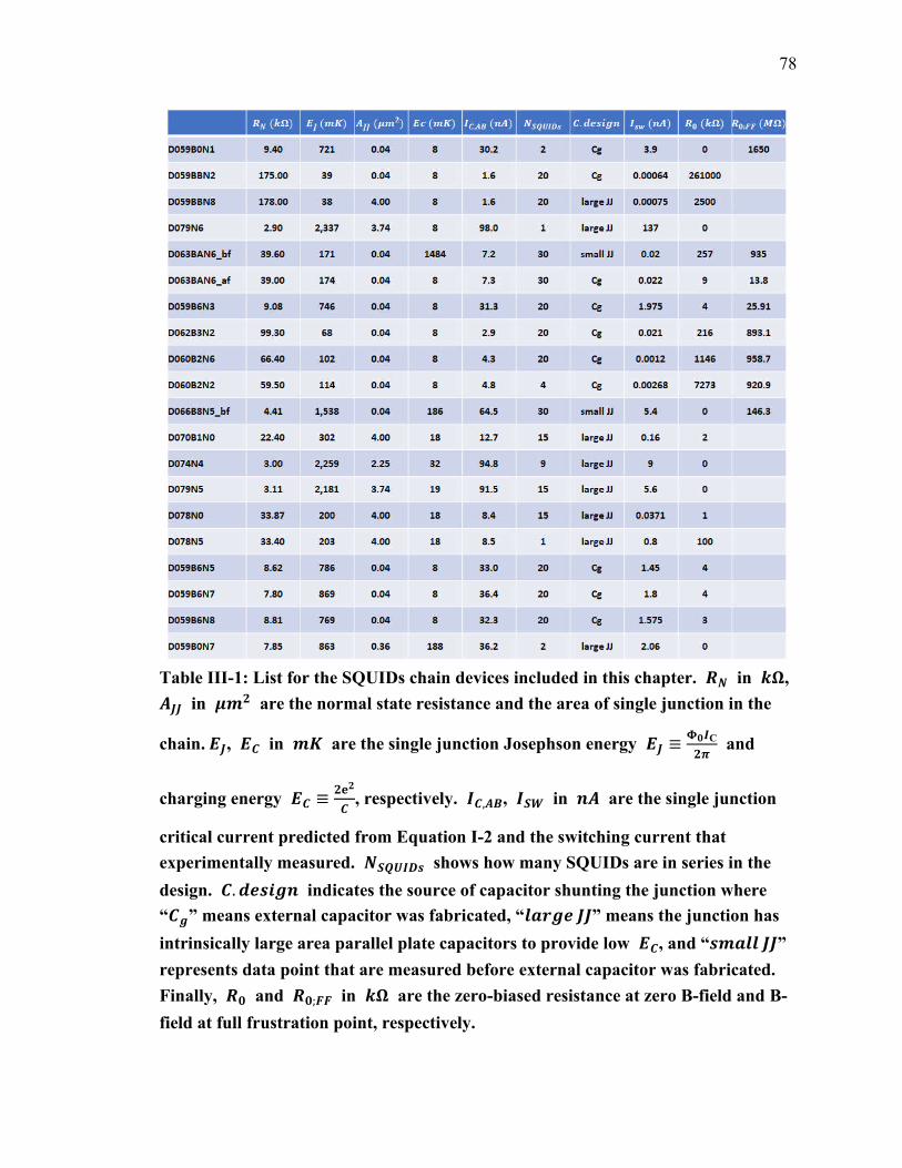
78
Table III-1: List for the SQUIDs chain devices included in this chapter. in ,
in are the normal state resistance and the area of single junction in the
chain. , in are the single junction Josephson energy ≡C
and
charging energy ≡
, respectively. ,, in are the single junction
critical current predicted from Equation I-2 and the switching current that
experimentally measured. shows how many SQUIDs are in series in the
design. . indicates the source of capacitor shunting the junction where
“” means external capacitor was fabricated, “ ” means the junction has
intrinsically large area parallel plate capacitors to provide low , and “ ”
represents data point that are measured before external capacitor was fabricated.
Finally, and ; in are the zero-biased resistance at zero B-field and B-
field at full frustration point, respectively.

79
Table III-2: List for the SQUIDs devices from literatures [24, 64, 65, 74-86], the
source can be found by following the Ref. # in Chapter VIII.
Our observations are in line with an expected strong dependence of the TAPS rate
on the sample parameters in the regime ≪ ≤ ≪ ∆. Indeed, one can estimate the
TAPS rate as Γ = −
, where is the plasma frequency (or an attempt rate)
and −
is the probability of the over-the-barrier excitation. For example, at
= 0.25 and
= 1.32 , the rate decreases from 3 × 10 to 0.1 if
80
the physical temperature decreases from 50 to 20 . This also explains why the
experimental results might be so sensitive to the noise level in the experimental setup.
III.6 Conclusion and outlook
Phase slips in JJs have been actively studied over the last three decades in different
types of Josephson circuits (single JJs, JJ arrays, etc.) over wide ranges of and . In
our work we focused on the thermally activated phase slips (TAPS), which, in contrast to
the quantum (a.k.a. coherent) phase slips, result in dissipation. At sufficiently low
temperatures ≪ ∆, where the concentration of quasiparticles becomes negligibly low,
the TAPS are expected to be the only source of dissipation.
We observed that in all studied devices with < 1 the switching current
is significantly suppressed with respect to . At the same time, we observed a very
rapid growth of with decreasing Josephson coupling below ≈ 1. Large scattering
of the data might reflect a steep dependence of the rate of incoherent phase slips on the
physical temperature and noise level in different experimental setups. Our observations are
in line with most of the data reported in literature.
The observed enhanced dissipation in Josephson circuits with < 1 imposes
limitations on the performance of superconducting qubits based on low- junctions. This
81
important issue requires further theoretical and experimental studies. Especially important
direction would be measurements of the coherence time in the qubits with systematically
varied Josephson energy over the range = 0.1 − 1. One of the signatures of TAPS-
induced decoherence is an observation of a steep temperature dependence of the coherence
time at < 100 [87].

82
MICRORESONATORS FABRICATED FROM HIGH-KINETIC-
INDUCTANCE ALUMINUM FILMS
This chapter is based on a joint work with W. Zhang, K. Kalashnikov, P. Kamenov, T.
DiNapoli and M.E. Gershenson (Rutgers University) [18]. My main contribution to this
work was the development of fabrications, microwave characterization techniques, and
data analysis. In this chapter, we will be investigating the MW response of disordered
superconducting thin films by characterizing the coplanar waveguide resonators made from
granular () films.
IV.1 Introduction
The development of novel quantum circuits for information processing requires the
implementation of ultra-low-loss microwave resonators with small dimensions [88].
Superconducting resonators have become ubiquitous parts of high-performance
superconducting qubits [89, 90] and kinetic-inductance photon detectors [39]. An
important resource for resonator miniaturization is the kinetic inductance of
superconductors, , which can exceed the magnetic ("geometrical") inductance by orders
of magnitude in narrow and thin superconducting films [39]. High kinetic inductance
translates into a high impedance of the MW elements, slow propagation of
83
electromagnetic waves, and small dimensions of the MW resonators. Ultra-narrow wires
and thin films of and [39, 40], [41], [42, 43], and granular
[44] were studied recently as candidates for high- applications. Research in high-
elements also have an important fundamental aspect. According to the Mattis-Bardeen
(MB) theory [91], the kinetic inductance of a thin superconducting film ( = 0) is
proportional to the resistance of the film in the normal state, , and thus increases with
disorder. This theory, however, cannot be directly applied to strongly disordered
superconductors near the disorder-driven superconductor-to-insulator transition (SIT).
Recent theories predict a rapid decrease of the superfluid density near the SIT and the
emergence of sub-gap delocalized modes that would result in enhanced dissipation at
microwave frequencies [47, 92]. Thus, the study of the electrodynamics of strongly
disordered superconductors may also contribute to a better understanding of the disorder-
driven SIT.
In this Chapter, we present a detailed characterization of the half-wavelength
microwave resonators fabricated from disordered Aluminum films. Our interest in high-
films was stimulated by the possibility of fabrication of superinductors (dissipationless
elements with microwave impedance greatly exceeding the resistance quantum =
()
[15, 93, 94]), and the development of SI-based protected qubits [17]. We have fabricated
84
resonators with an impedance as high as 5kΩ, ultra-small dimensions and relatively
low losses. The study of the temperature dependences of the resonance frequency and
intrinsic quality factor at different MW excitation levels allowed us to identify
resonator coupling to two-level systems (TLS) in the environment as the primary
dissipation mechanism at ≲ 250mK; at higher temperatures the losses can be attributed
to thermally excited quasiparticles.
IV.2 Experimental details
IV.2-1 Design and fabrication
Preparations of disordered films
The standard method for the fabrication of disordered films is the deposition
of at a reduced oxygen pressure [95, 96]. Such films consist of nanoscale grains (3 ÷
4 in diameter) partially covered by . We have fabricated the films by DC
magnetron sputtering of an 6N-purity target in the atmosphere of and .
Typically, the partial pressures of and were 5 × 10mbar and (3 ÷ 7) ×
10 mbar, respectively. The films were deposited onto the intrinsic substrates at
room temperature. By controlling the deposition rate and pressure, the resistivity of the
studied films can be tuned between 10Ωcm and 10Ωcm . In order to improve
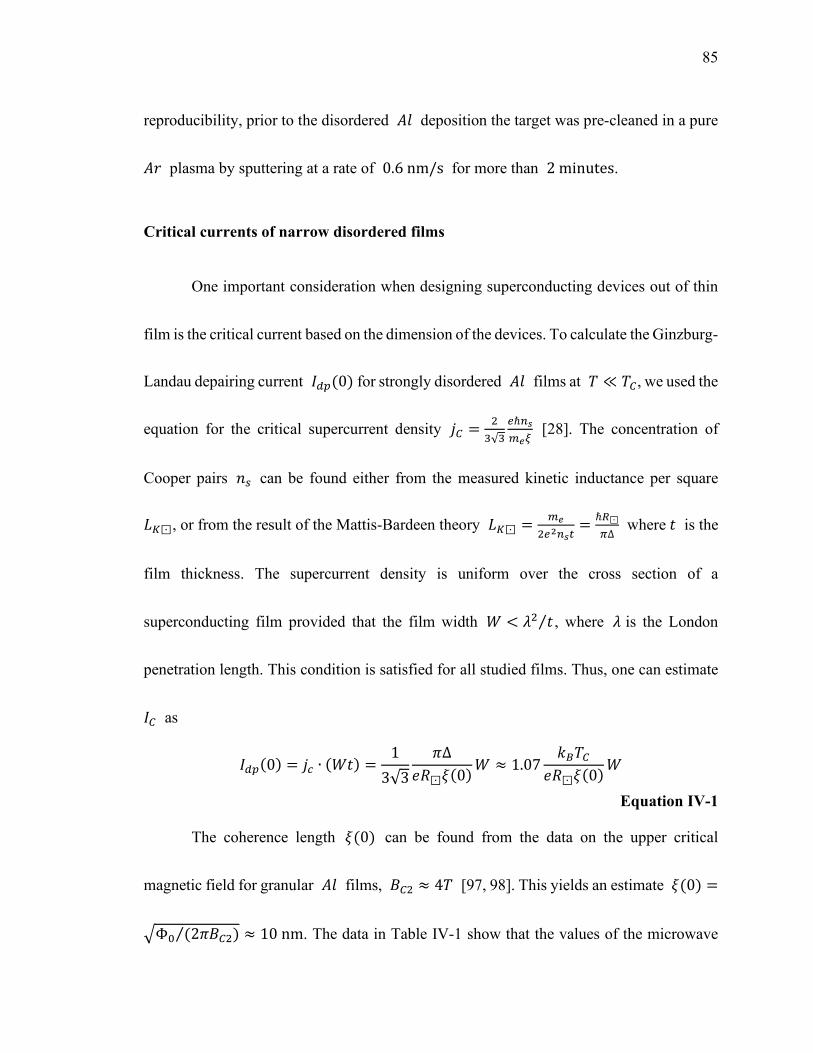
85
reproducibility, prior to the disordered deposition the target was pre-cleaned in a pure
plasma by sputtering at a rate of 0.6 nm/s for more than 2 minutes.
Critical currents of narrow disordered films
One important consideration when designing superconducting devices out of thin
film is the critical current based on the dimension of the devices. To calculate the Ginzburg-
Landau depairing current (0) for strongly disordered films at ≪ , we used the
equation for the critical supercurrent density =
√
ℏ
[28]. The concentration of
Cooper pairs can be found either from the measured kinetic inductance per square
⊡, or from the result of the Mattis-Bardeen theory ⊡ =
=
ℏ⊡
∆ where is the
film thickness. The supercurrent density is uniform over the cross section of a
superconducting film provided that the film width < ⁄ , where is the London
penetration length. This condition is satisfied for all studied films. Thus, one can estimate
as
(0) = ∙ () =1
3√3
∆
⊡(0) ≈ 1.07
⊡(0)
Equation IV-1
The coherence length (0) can be found from the data on the upper critical
magnetic field for granular films, ≈ 4 [97, 98]. This yields an estimate (0) =
Φ (2)⁄ ≈ 10 nm. The data in Table IV-1 show that the values of the microwave
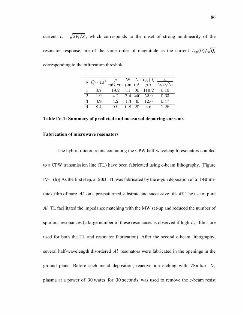
86
current ∗ = 2∗ ⁄ , which corresponds to the onset of strong nonlinearity of the
resonator response, are of the same order of magnitude as the current (0) ⁄
corresponding to the bifurcation threshold.
Table IV-1: Summary of predicted and measured depairing currents
Fabrication of microwave resonators
The hybrid microcircuits containing the CPW half-wavelength resonators coupled
to a CPW transmission line (TL) have been fabricated using e-beam lithography. [Figure
IV-1 (b)] As the first step, a 50Ω TL was fabricated by the e-gun deposition of a 140nm-
thick film of pure on a pre-patterned substrate and successive lift-off. The use of pure
TL facilitated the impedance matching with the MW set-up and reduced the number of
spurious resonances (a large number of these resonances is observed if high- films are
used for both the TL and resonator fabrication). After the second e-beam lithography,
several half-wavelength disordered resonators were fabricated in the openings in the
ground plane. Before each metal deposition, reactive ion etching with 75mbar
plasma at a power of 30 watts for 30 seconds was used to remove the e-beam resist

87
residue from the substrate surface. The width of the central strip of the resonators varied
between 0.5 ÷ 10µm, and the strip-ground distance was fixed at 4µm with lithography
alignment precision < 0.5μm. [Figure IV-1 (a)]
Figure IV-1: (a) Microphotograph of a portion of the halfwavelength resonator
capacitively coupled to the coplanar waveguide transmission line. Light green - Al
ground plane and the central conductor of the transmission line, green - silicon
substrate, black - the central strip of the resonator made of strongly disordered Al.
(b) Several resonators with different resonance frequencies coupled to the
transmission line
For the resonator characterization at ultra-low temperatures, we used a microwave
setup developed for the study of superconducting qubits [15]. The resonators were designed
with the resonance frequencies ≈ 2 ÷ 4GHz, which allowed us to probe the first three
harmonics of the resonators within the setup frequency range 2 ÷ 12GHz . Different
resonance frequencies of the resonators enabled multiplexing in the transmission
measurements. In order to ensure accurate extraction of the internal quality factor , the

88
resonators were designed with a coupling quality factor of the same order of
magnitude as .
IV.3 Measurement and microwave analysis
The resonators in this work were characterized using a wide range of MW power
, two-tone (pump-probe) measurements, and time domain measurements. The
resonator parameters , , and were found from the simultaneous measurements of
the amplitude and the phase of the transmitted signal () using the procedure
described in [89, 90]. The kinetic inductance of the central conductor of the resonators,
which exceeded the magnetic inductance by several orders of magnitude, was calculated
as = 14
(the capacitance between the resonator strip and the ground was
obtained from the Sonnet simulations). The parameters of several representative resonators
are listed in Table IV-2.
Table IV-2: Summary of the measured parameters of resonators
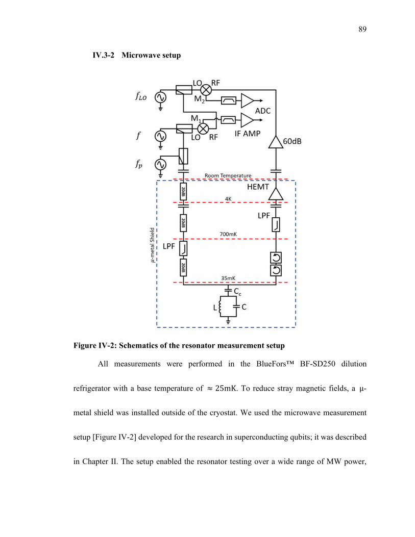
89
IV.3-2 Microwave setup
Figure IV-2: Schematics of the resonator measurement setup
All measurements were performed in the BlueFors™ BF-SD250 dilution
refrigerator with a base temperature of ≈ 25mK. To reduce stray magnetic fields, a µ-
metal shield was installed outside of the cryostat. We used the microwave measurement
setup [Figure IV-2] developed for the research in superconducting qubits; it was described
in Chapter II. The setup enabled the resonator testing over a wide range of MW power,
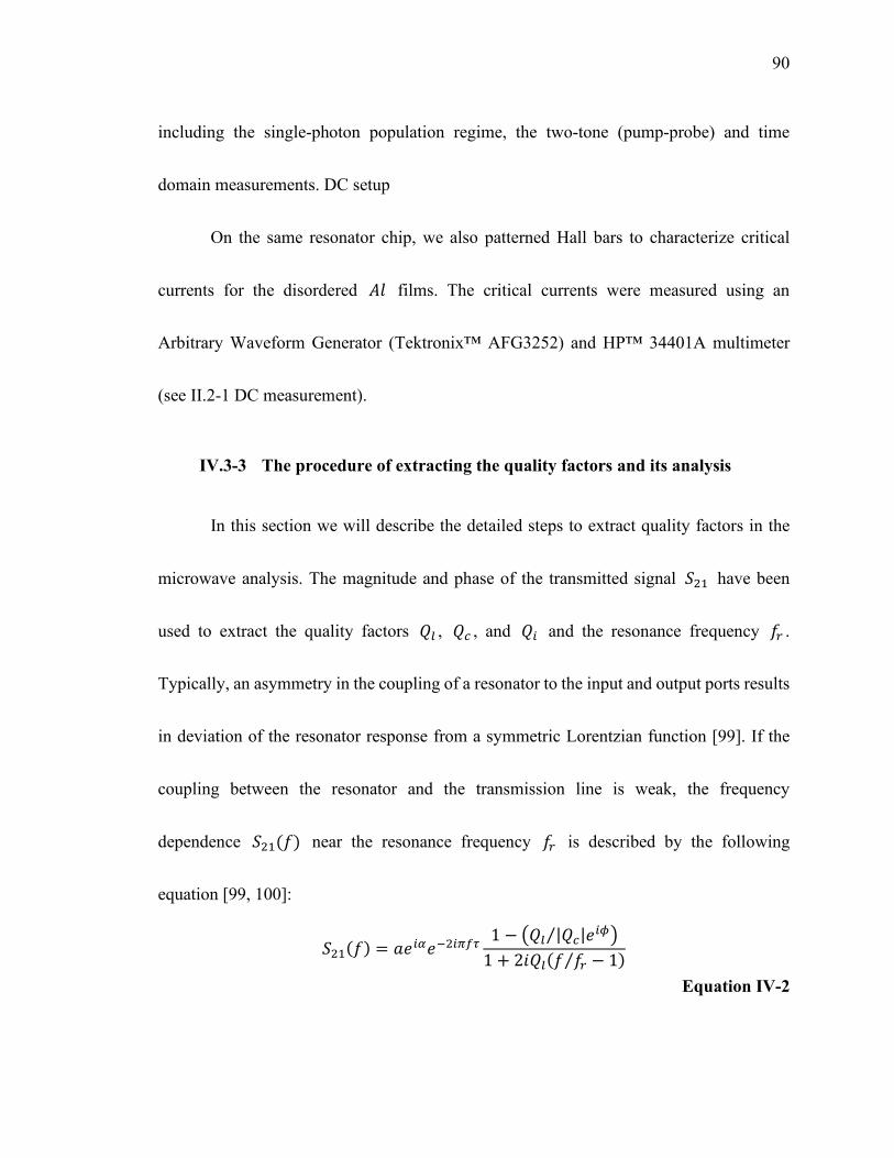
90
including the single-photon population regime, the two-tone (pump-probe) and time
domain measurements. DC setup
On the same resonator chip, we also patterned Hall bars to characterize critical
currents for the disordered films. The critical currents were measured using an
Arbitrary Waveform Generator (Tektronix™ AFG3252) and HP™ 34401A multimeter
(see II.2-1 DC measurement).
IV.3-3 The procedure of extracting the quality factors and its analysis
In this section we will describe the detailed steps to extract quality factors in the
microwave analysis. The magnitude and phase of the transmitted signal have been
used to extract the quality factors , , and and the resonance frequency .
Typically, an asymmetry in the coupling of a resonator to the input and output ports results
in deviation of the resonator response from a symmetric Lorentzian function [99]. If the
coupling between the resonator and the transmission line is weak, the frequency
dependence () near the resonance frequency is described by the following
equation [99, 100]:
() = 1 − ||⁄
1 + 2( ⁄ − 1)
Equation IV-2

91
The phase delay can be found from the value of
[()] measured over
a range of away from the resonance. All other parameters in [Equation IV-2] have been
determined similar to the iteration procedure described in [100]. We first selected the initial
values of unknown parameters in [Equation IV-2] and ran a multi-variable nonlinear fitting
procedure for the entire model. The output of the nonlinear fit was used to obtain the final
values of unknown parameters and the error bars. The parameter initialization procedure
was as follows. After elimination of the phase delay , the data () formed a
circle on the -plane [Figure IV-3 (a)]. The prefactor corresponds to the center of
this circle. For the normalized circle
∗ = () ⁄
Equation IV-3
the angle between the off-resonance points and the I-axis corresponds to , and the circle
diameter corre ponds to the ratio of ||⁄ [Figure IV-3 (b)]. Next, we translated ∗
so that the circle center coincided with the origin. can then be obtained from fitting the
phase of the translated ∗ , , versus frequency with = + tan[2(1 − ⁄ )]
(see Figure IV-3 (c)). Figure IV-3 (d,e) show the experimental data with the result of fitting.
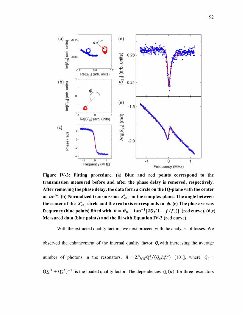
92
Figure IV-3: Fitting procedure. (a) Blue and red points correspond to the
transmission measured before and after the phase delay is removed, respectively.
After removing the phase delay, the data form a circle on the IQ-plane with the center
at . (b) Normalized transmission ∗ on the complex plane. The angle between
the center of the ∗ circle and the real axis corresponds to . (c) The phase versus
frequency (blue points) fitted with = + [( − ⁄ )] (red curve). (d,e)
Measured data (blue points) and the fit with Equation IV-3 (red curve).
With the extracted quality factors, we next proceed with the analyses of losses. We
observed the enhancement of the internal quality factor with increasing the average
number of photons in the resonators, = 2Q (ℎ
)⁄ [101], where =
(Q + Q
) is the loaded quality factor. The dependences () for three resonators

93
with different measured at the base temperature ≈ 25mK are shown in Figure IV-4.
Similar behavior of () have been observed for many types of CPW superconducting
resonators (see, e.g. [28, 102] and references therein), including the resonators based on
disordered films [44, 103]. Note that the increase of with the input MW power
is limited by the resonance distortion by bifurcation at > ∗. For the resonators
with ≳ 10 the onset of bifurcation is observed for the microwave currents ∗ =
2∗ ⁄ which scale approximately as ⁄ [104], where is the Ginzburg-
Landau depairing current in the central strip in the previous section (Equation IV-1).
Figure IV-4 The dependences () at ≈ for the resonators with different
widths. Solid curves represent the theoretical fits of the quality factor governed by
TLS losses [Equation IV-5].
The power-dependent intrinsic losses can be attributed to the resonator coupling to
the TLS with the Lorentzian shaped distribution
94
() ≈1
( − ℎ) + (ℏ ⁄ )
Equation IV-4
where is the energy of TLS and is its dephasing time [105]. Once the MW power
reaches some characteristic level and the Rabi frequency of the driven TLS
Ω ≈ exceeds the relaxation rate 1 √⁄ , the population of the excited TLS
increases, and the amount of energy that the TLS with ≈ can absorb from the
resonator decreases. Thus, the high "burns the hole" in the density of states (DoS)
of dissipative TLS. The width of the "hole" is 2⁄ , the power-dependent factor can be
written as
= 1 +
Equation IV-5
where and correspond to and , respectively. Note that the exponent is
known to be dependent on the electric field distribution in a resonator [106], and the
characteristic power increases with temperature by orders of magnitude due to a strong
-dependence of and [107]. Taking into account the TLS saturation at high
temperature, the power dependence of the TLS-related part of the loss tangent can be
expressed as follows [12]:
(, ) =
ℎ
ℎ
2
Equation IV-6

95
By fitting the experimental data with Equation IV-6 we found and , the
obtained parameters are listed in Table IV-3. We found that larger values of correspond
to wide strips, and the extracted scales as the square of the electric field on the surface
of the resonator. The experimental dependences () measured for resonators #2 − 4 at
≅ 1 and ≫ 1 [Equation IV-8(b)] are well described by the sum of the TLS
contribution [Equation IV-6] and the MB term = () ()⁄ [43]:
() = , , , + (, (0))
Equation IV-7
The agreement of measured with the prediction of Equation IV-7 over the whole
measured temperature range proves that the losses in the developed resonators are limited
by the sum of TLS and MB terms.
Table IV-3: Summary of the fitting parameters
IV.4 Discussion
The measured sheet kinetic inductance ⊡ = 2 nH ⊡⁄ is similar to that reported
for granular films in [103] and in [108], and exceeds by a factor-of-2 ⊡
realized for ultra-thin disordered films of [42, 109]. For the disordered films

96
with < 10mΩ · cm, ⊡ is in good agreement with the result of the MB theory [42],
⊡( = 0) = ℏ⊡ ∆(0)⁄ , where ∆(0) is the BCS energy gap at = 0K. Very large
values of ⊡ allowed us to realize the characteristic impedance = ⁄ as high as
5 kΩ for the resonators with narrow ( = 0.7µ) central strips. The speed of propagation
of the electromagnetic waves in such resonators does not exceed 1% of the speed of light
in free space; accordingly, their length is two orders of magnitude smaller than that for the
conventional CPW resonators with the impedance = 50 Ω.
To identify the physical mechanisms of losses in the resonators, we measured the
dependences of and on the temperature ( = 25 ÷ 450 mK) and the microwave
power . Below we show that in the case of moderately disordered films (resonators
#2 − 4), both the dissipation and dispersion at < 0.25K can be attributed to the resonator
coupling to the TLS in the environment, whereas at higher temperatures they are controlled
by the T dependence of the complex conductivity of superconductors, () = () −
() [42].
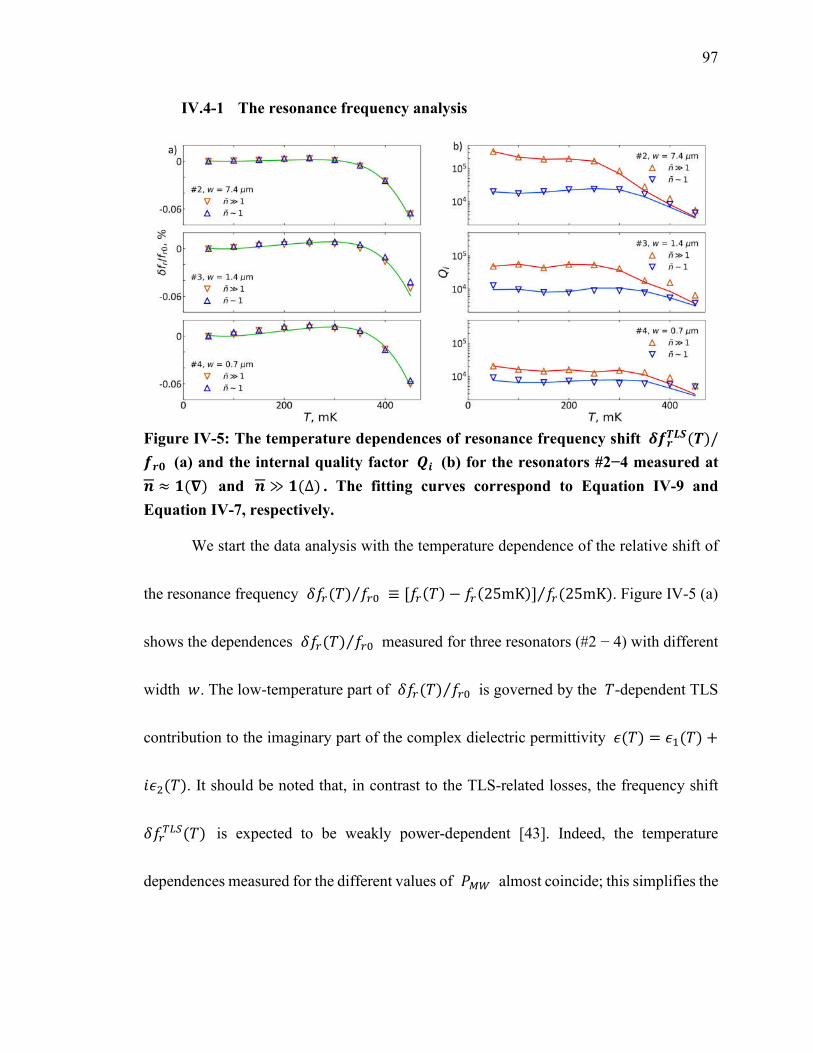
97
IV.4-1 The resonance frequency analysis
Figure IV-5: The temperature dependences of resonance frequency shift
()/
(a) and the internal quality factor (b) for the resonators #2−4 measured at
≈ () and ≫ (∆) . The fitting curves correspond to Equation IV-9 and
Equation IV-7, respectively.
We start the data analysis with the temperature dependence of the relative shift of
the resonance frequency () ⁄ ≡ [() − (25mK)] (25mK)⁄ . Figure IV-5 (a)
shows the dependences () ⁄ measured for three resonators (#2 − 4) with different
width . The low-temperature part of () ⁄ is governed by the -dependent TLS
contribution to the imaginary part of the complex dielectric permittivity () = () +
(). It should be noted that, in contrast to the TLS-related losses, the frequency shift
() is expected to be weakly power-dependent [43]. Indeed, the temperature
dependences measured for the different values of almost coincide; this simplifies the

98
analysis and reduces the number of fitting parameters. The low-temperature part of
() is well described by the following equation [39]:
()
=
ℜ
1
2+
1
2
ℎ
−
ℎ
Equation IV-8
Here Ψℜ() is the real part of the complex digamma function, the TLS
participation ratio, is the energy stored in the TLS-occupied volume normalized by the
total energy in the resonator, and the loss tangent characterizes the TLS-induced
microwave loss in weak electric fields at low temperatures ≪ ℎ . The product
is the only fitting parameter, its values are listed in Table IV-3. The obtained values of
are close to that found for -based [43] and -based resonators [108, 110].
Note that resonator #4 demonstrates the most pronounced increase of () with
temperature due to the stronger electric fields and a larger participation ratio characteristic
of the high- resonators [12].
At > 0.25 K, rapidly drops due to the decrease of the superfluid density. The
dependences () over the whole studied range can be described as
() ⁄ = () ⁄ +
() ⁄
Equation IV-9
where
99
()
=
1
2() − (25)
(25)
Equation IV-10
is the resonance shift due to the -induced break of Cooper pairs and subsequent increase
of the kinetic inductance, calculated in the thin film limit [43]. The only free parameter in
() ⁄ is the gap energy ∆(0), which can be found by fitting of the high- portion
of () ⁄ [Equation IV-9]; the measured ratio ∆(0) = is about 10% greater
than the BCS value of 1.76 , which is consistent with previously reported data [62].
IV.4-2 In-depth analysis of () and () fitting
To identify the dominant mechanisms of losses in the studied resonators, we have
analyzed the experimental dependences () and () on the basis of the theory of
two-level systems [111] and the Mattis-Bardeen theory of the complex impedance of
superconductors [91].
The losses due to the real part of the complex impedance of superconductors, =
− , can be estimated using the Mattis-Bardeen theory. In the thin film limit [112]:
() = () ()⁄ ; where
() =
ℎ [() − ( + ℎ)] ×
( + + ℎ)
√ − ( + ℎ) −
() =
ℎ [1 − 2( + ℎ)] ×
( + + ℎ)
√ − ( + ℎ) −
Equation IV-11

100
() is Fermi-Dirac distribution function, Δ(0) is the energy gap. The temperature-
dependent shift of the resonance frequency is given in the previous section by Equation
IV-10. Since the frequency shift () does not depend on the MW power, the fitting
procedure included the following steps:
• fitting the () dependence with only two free parameters: Δ(0) (which controls
the behavior of () term at > 300mK), and the product of the participation ratio
and the material loss tangent, (which governs the rising part of ());
• finding the index from the linear part of () at = 25 plotted on the
double-log scale.
• knowing , , Δ(0), one can find the low temperature characteristic power (i.e.
the number of photons (0)) using () measured at the base temperature = 25mK;
• finding () by fitting () data for both low and high values of the input power.
Significant change in the population of the ground and excited TLS states due to
Rabi oscillations is expected at the average number of photons in the resonator > .
The characteristic value ≈ 1 ⁄ depends on the TLS relaxation time () and
the dephasing time (). In agreement with [113] where the TLS relaxation time was
shown to be , ≈ 1 + , we found that the extracted characteristic values of
depend on the temperature as () = (0) + , ≈ 2 [Figure IV-6].
101
Figure IV-6: The temperature dependences of for different resonators.
IV.4-3 The two-tone time-domain measurements and telegraph noise
We obtained an additional information on the TLS related dissipation by
performing the pump-probe experiments in which was measured at a low-power ( ≈
1) probe signal while the power of the pump signal at the frequency was varied
over a wide range. Figure IV-7 (a) shows the dependences () measured at different
detuning values ∆ = − = 0, ±1, ±10MHz. Note that we have not observed any
changes in when the pump signal was applied at the second and third harmonics of the
resonator. Also, was -independent when we monitored the second harmonic and
applied the pump signal at the first harmonic.

102
Figure IV-7: (a) The dependences of for resonator #1 on the pump tone power
for several values of detuning ∆ between resonance and pump frequencies. (b)
The values of measured versus detuning ∆ at a fixed number of the pump tone
photons in the resonator ≈ .
Since the resonator coupling to the pump signal varies by several orders of
magnitude within the detuning range 0 ÷ 10, it is more informative to analyze
as a function of the average number of the "pump" photons in the resonator, =
1 −
− ()
ℎ , where and = 1 − are the
transmission and reflection amplitudes at the pump frequency, respectively. The
dependence on the detuning ∆ for a fixed ≈ 1000 is depicted in Figure IV-7
(b). The resonance behavior of (∆) is expected since only a narrow TLS band
[Equation IV-4] contributes to dissipation: the "hole" extension in the DoS is limited by
≈ ⁄ around the pump frequency. Indeed, using the approach developed in [114], one
can obtain the following expression:
(∆) = 1 +( 2⁄ )
∆ + (1 2⁄ )

103
where is the off-resonance quality factor and introduced by Equation IV-5 factor κ
might be calculated as = ⁄ . The dephasing time is the only fitting parameter,
and it is found to be ≈ 60ns. This result agrees with the measurements of the dephasing
time for individual TLS in amorphous tunnel barrier in Josephson junctions [10].
By application of the MW pulses at the pump frequency, we observed that the
characteristic time at which varies with does not exceed 36 . For several
resonators we have observed the telegraph noise in the resonance frequency on the time
scale of 1 ÷ 10. This noise can be attributed to interactions of the resonators with a small
number of strongly coupled TLS.
Interactions between the high-frequency (coherent, > ) TLS with the low-
frequency (thermal, < ) fluctuators result in the TLS spectral diffusion as well as
the flicker noise. The telegraph noise in the resonance frequency is expected if some
of the TLS with ≈ are strongly coupled to a resonator. Typical TLS densities for
/ junctions are ≈ 1 (GHz · µm) −1 [11]. Interestingly, the number of
strongly coupled TLS for our resonators (assuming that the strongly coupled TLS are in
the oxide layer of the resonator) is of the order of unity (1 (GHz · µm) × 0.1MHz ×
10µm ). To study the telegraphy noise, we repetitively measured at a fixed
frequency on a slope of the resonance dip for a few minutes. Figure IV-8 shows an example
104
of the measured telegraph noise in Re[] . The characteristic time scale of random
switching between two Re[] levels is 1 ÷ 10s.
Figure IV-8: The time dependence of [] measured at = at a fixed
frequency on the slope of a resonance dip. The microwave power corresponds to
⟨⟩ ≈ . Each point corresponds to the data averaging over .
IV.4-4 Scaling of ()
The ground and excited states of TLS become equally populated when the Rabi
oscillation frequency Ω = · ℏ⁄ exceeds the rate 1 ⁄ , or, equivalently, when the
electric field in the TLS-occupied volume exceeds the critical value ≈ ℏ ⁄ .
In order to understand the variation of the observed characteristic power for different
resonators, we considered the dependence of the maximum electric field near the surface
on the resonator parameters.
105
The standard way to evaluate the characteristics of CPW resonators is by the
Schwarz-Cristoffel (SC) mapping of the coplanar topology to the trivial parallel-plate
capacitor geometry. Let us consider a zero-thickness CPW with a central strip width 2
and a ground-to-ground distance 2. The transfer function for the mapping of the upper
half-plane to the rectangle is given by
() =
( − )( + )( − )( + )
here is an integration constant, chosen to be = 1. The half-width of the equivalent
capacitor is calculated as
= () =1
(1 − )(1 − )
≡1
()
() is also known as the complete elliptic integral of the first kind, = ⁄ . Similarly,
the height of the capacitor is
=1
(1 − )(1 − )
⁄
≡1
1 −
the electric field in the -plane for the given voltage across the capacitor is uniform
and can be easily obtained as
=
=
√1 −
the corresponding field in the -plane scales with the factor () = ⁄ which is
() =1
( − )( − )
thus, for example, the field strength at the center of microstrip is
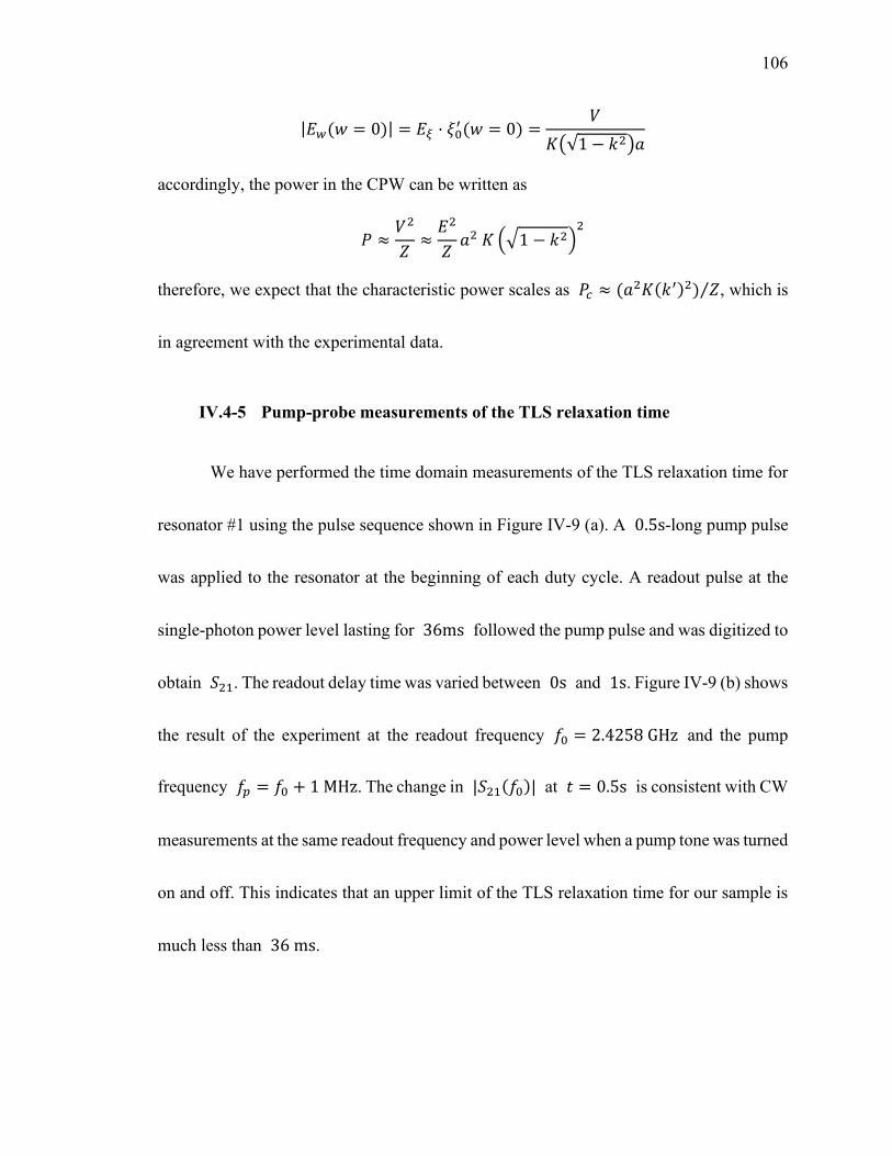
106
|( = 0)| = · ( = 0) =
√1 −
accordingly, the power in the CPW can be written as
≈
≈
1 −
therefore, we expect that the characteristic power scales as ≈ (()) ⁄ , which is
in agreement with the experimental data.
IV.4-5 Pump-probe measurements of the TLS relaxation time
We have performed the time domain measurements of the TLS relaxation time for
resonator #1 using the pulse sequence shown in Figure IV-9 (a). A 0.5s-long pump pulse
was applied to the resonator at the beginning of each duty cycle. A readout pulse at the
single-photon power level lasting for 36ms followed the pump pulse and was digitized to
obtain . The readout delay time was varied between 0s and 1s. Figure IV-9 (b) shows
the result of the experiment at the readout frequency = 2.4258 GHz and the pump
frequency = + 1 MHz. The change in |()| at = 0.5s is consistent with CW
measurements at the same readout frequency and power level when a pump tone was turned
on and off. This indicates that an upper limit of the TLS relaxation time for our sample is
much less than 36 ms.
107
Figure IV-9: (a) The pulse sequence. (b) The time dependence of || measured at
= . . The pump pulse at = + was applied between =
and = . . The pump tone power corresponds to ¯ ≈ . Each data
point was averaged over 4000 cycles with the same readout delay time. The inset
shows CW measurement of versus with (red) and without (blue) the pump
signal and indicates the position of used in the relaxation time measurement. The
readout power was at the single photon level for all measurements on this plot.
IV.5 Summary
In conclusion, we have fabricated CPW half wavelength resonators made of
strongly disordered films. Because of the very high kinetic inductance of these films,
we were able to significantly reduce the length of these resonators, down to ≈ 1% of that
of conventional CPW resonators with a 50Ω impedance. Due to ultra-small dimensions
108
and relatively low losses at mK temperatures, these resonators are promising for the use
in quantum superconducting circuits operating at ultralow temperatures, especially for the
applications that require numerous resonators, such as multi-pixel MKIDs [28, 104]. The
high impedance = ⁄ of the narrow resonators can be used for effective coupling
of spin qubits [115, 116]. The high resonator impedance imposes limitations on the strength
of resonator coupling to the transmission line. For the studied CPW resonators with ≈
5 kΩ, the strongest realized coupling (when half of the resonator length was used as the
element of capacitive coupling to the transmission line) corresponded to ≈ 10. On the
other hand, for many applications, such as large MKID arrays that require a high loaded
factor, this should not be a limitation.
We have shown that the main source of losses in these resonators at ≪ is the
coupling to the resonant TLS. A comparison of our results with those of the other groups
shows that the obtained values, increasing from (1 ÷ 2) × 10 in the single-photon
regime to 3 × 10 at high microwave power, are typical for the CPW superconducting
resonators with similar TLS participation ratios. This implies that the disorder in films
does not introduce any additional, anomalous losses. Most likely, the relevant TLS are
located near the edges of the central resonator strip either in the native oxide on the
substrate surface or in the amorphous oxide covering the films. Further increase of can

109
be achieved by the methods aimed at the reduction of surface participation, such as
substrate trenching (see [117] and references within) and increasing the gap between the
center conductor and the ground plane [106]. The evidence for that was provided by the
results of [103] obtained for the modified three-dimensional microstrip structures based on
disordered films. It is also worth mentioning that the losses can be reduced using TLS
saturation by the microwave signal outside of the resonator bandwidth but within the TLS
spectral diffusion range. A fundamental issue pertinent to all strongly disordered
superconductors is the development of a better understanding of the impedance of
superconductors near the disorder-driven SIT. This issue requires further research, and the
microwave experiments with the resonators made of disordered and other disordered
materials demonstrating the SIT may shed light on the nature of this quantum transition.

110
FLUXON-PARITY-PROTECTED SUPERCONDUCTING QUBIT
This chapter is based on joint work with K. Kalashnikov, P. Kamenov, and M.E.
Gershenson (Rutgers University), W.T. Hsieh and M.Bell (University of Massachusetts
Boston), and A. Di Paolo and A. Blais (Universite de Sherbrooke) [14]. My main
contribution to this work was the development of fabrications and microwave
characterization techniques.
V.1 Introduction
Over the past two decades superconducting qubits have emerged as one of the most
promising platforms for quantum computing, and the coherence of these qubits has been
improved by five orders of magnitude [88, 118]. Even with this spectacular progress,
implementation of error correction codes remains challenging [119]. Further improvement
in coherence will require the development of new approaches for mitigating harmful effects
due to uncontrollable microscopic degrees of freedom, such as two-level systems (TLSs)
in the qubit environment [11]. This route is provided by the improvement of materials for
fabrication of superconducting qubits, which can lead to the reduction of the TLS density.
A complementary approach, which we consider in this work, is based on the reduction of
the qubit-TLS coupling by qubit design.

111
V.2 Suppressing the decoherence
Qubit coherence is characterized by the energy relaxation (decay) time and the
dephasing time . The decay rate Γ ≡ 1 ⁄ due to coupling to a fluctuating parameter
is proportional to the transition amplitude |⟨|ℋ|⟩| , where ℋ is the coupling
Hamiltonian and |⟩ and |⟩ are the qubit’s ground state and first excited state,
respectively. Since the external noise couples to local operators, decreasing of the overlap
of |⟩ and |⟩ wavefunctions can significantly reduce Γ. This strategy is exploited by
several qubit designs in which localization of the logical-state wavefunctions occurs within
distinct and well-separated minima of the qubit potential, such as the “heavy fluxonium”
qubit [120, 121].
On the other hand, a small dephasing rate Γ ≡ 1 ⁄ requires the qubit transition
frequency to be insensitive to fluctuations of . The first-order decoupling of a qubit
from noise has been achieved at the so-called “sweet spot” , where ⁄ |= 0
[122]. However, the coherence times achieved with this approach are insufficient for the
implementation of the error correction codes, even if the drifts of the qubit operating point
are eliminated over the timescale of operations. To remedy this, a “sweet-spot-everywhere”
approach has been realized in the transmon qubit [5, 123]: an exponentially strong

112
suppression of the qubit sensitivity to noise has been achieved by delocalization of the
qubit wavefunctions in charge space.
It is, however, worth noting that the two approaches of and protection by
qubit design come into conflict in the case of devices with a single degree of freedom in
the qubit Hamiltonian (which we refer to as 1D qubits). For instance, at the dephasing
sweet spot of the “heavy fluxonium” [120, 121] wavefunctions become delocalized due to
its hybridization, which limits the decay time (Figure V-1 (a), = 1 ), whereas
protection can be realized only at the slope of the dispersion curve where is small
(Figure V-1 (a), = 2 ). In turn, the charge insensitivity of the transmon qubit is
accompanied with strong dipole matrix elements that limit (Figure V-1 (b), = 3, 4).
Additionally, the flatness of the transmon-qubit bands results in a strong reduction of the
spectrum anharmonicity, potentially leading to a leakage of information outside of the
computational subspace [124]. These examples suggest that a qubit Hamiltonian with full
noise protection against relaxation and dephasing, i.e., exponentially large and ,
cannot be implemented in a single-mode superconducting quantum device. This conflict,
however, can be reconciled by the so-called “few body” qubits [13] that incorporate more
than one degree of freedom in the qubit Hamiltonian (the dimensionality > 1) [16, 125-
127].

113
Figure V-1: The tradeoff between the decay and dephasing protection in
superconducting qubits with a single charge or flux degree of freedom. The band
structure (top panels) and wavefunctions (bottom panels) of a particle in
quasiperiodic potentials: (a) the free-particle regime and (b) the tight-binding regime.
The wavefunction overlap and the energy sensitivity ()
/ do not simultaneously
vanish for any point (i). Flux (charge) qubits correspond to the case in which the
control parameter = , kinetic energy = (), tunneling energy =
(), and |⟩ is a fluxon (charge) basis.
Another concept of qubit protection exploits symmetries of Hamiltonians with
> 1 [58], an example being the qubit based on Josephson rhombi arrays [128],
experimentally realized in [16]. In a single rhombus threaded by half of the magnetic flux
quantum, the transport of individual Cooper pairs (CPs) is suppressed due to destructive
Aharonov-Bohm interference, such that the rhombi chain supports correlated transport of
CPs (i.e., acts as a cos(2) Josephson element). The dephasing time of the qubit can be
114
enhanced by delocalization of wavefunctions over the states with the same CP parity,
which does not compromise . Importantly, this qubit design enables on-demand
switching of the qubit coupling to the environment (including the readout) on and off,
which facilitates qubit manipulations. This also provides a route to fault-tolerant gates
immune to noises in the control lines [129]. An improved version can be built by parallel
connection of several rhombi chains [130]
Here we focus on the implementation of a complementary circuit preserving the
parity of fluxon in a superconducting loop, which consists of a split Cooper-pair box (CPB)
and a superinductor (SI), and is depicted in Figure V-2 (a). The probability of single-fluxon
tunneling in and out of the loop can be tuned by the CPB charge of the CPB island
(hereafter we refer to CPB charge modulo 2 due to periodicity). At = 1 (where
is the electron charge) Aharonov-Casher interference results in a 4-periodic potential (a
cos(/2) Josephson element), which preserves the fluxon parity in the loop [17, 43, 131].
In the case of perfectly symmetric CPB junctions, the two degenerate logical states with
different fluxon-number parity reside in disjoint regions of the Hilbert space, forbidding
qubit decay. It is moreover possible to delocalize the wavefunction within each parity state
via double fluxon tunneling in order to provide protection against pure dephasing by flux
noise. Below we refer to such an element as a “bifluxon” qubit.

115
Figure V-2: (a) Simplified circuit scheme of the bifluxon qubit. Charging energies of
the superinductor and CPB are and , respectively. The qubit is controlled by
the CPB charge and the magnetic flux . (b) Optical image of the bifluxon
qubit, readout resonator, and the microwave transmission line. The inset shows the
SEM image of its central part: two JJs form the CPB island (red false color), the long
array of larger JJs acts as a superinductor (blue), the narrow wire (green) forms the
closed loop and couples the qubit to the readout resonator.
V.3 Experimental setups
In this work, the bifluxon qubit is realized as a split junction CPB (a
superconducting island flanked by two small and nominally identical JJs with Josephson

116
and charging energies and , respectively; see Figure V-2 (b)] shunted by a SI,
which is implemented as an array of = 122 larger JJs with corresponding energies
and . The sizes of small ( 0.11 × 0.16 ) and large ( 0.21 × 0.30 )
junctions are chosen in order to allow phase-slip events across the CPB junctions
(/ ≈ 1) but suppress the phase slips in the array (/ ≈ 1). As long as the
inductive energy of the SI chain = / is much smaller than , the phase across
the SI is close to an integer number of 2. The stray capacitance of the superconducting
islands to the ground in combination with the junction capacitances results in charging
energies and of the CPB and the SI, respectively. The self-resonant mode of the
SI with frequency , determined by the SI inductance and its stray capacitance to the
ground , should remain well above the qubit transition frequency (usually a few GHz)
in order to avoid qubit coupling to this mode.
The bifluxon qubit is controlled by the magnetic flux in the loop Φ and the
offset charge , induced by applying the dc bias voltage to the coupling capacitor
between the microstrip line and the CPB island. In order to perform the dispersive
measurements of the bifluxon qubit, the device is inductively coupled to a lumped element
readout resonator with capacitance = 120 and inductance = 4 . For the
coupling, a portion of the bifluxon superconducting loop with kinetic inductance =

117
0.4 is shared with the readout resonator. The qubit-resonator coupling constant for the
device described in this paper is /2 = 52MHz. The full list of experimental parameters
is provided below:
Table V-1: The bifluxon qubit parameters estimated from a test structure: Josephson
and charging energies, areas of the junctions in the CPB and SI array, and the
number of junctions in the array and its total inductance.
Table V-2: The resonator parameters: inductance, capacitance, shunting inductance,
and loaded and intrinsic quality factors.
Table V-3: The fitting parameters: the CPB junction Josephson energy, charging
energies of CPB and SI, the SI inductive energy, the CPB junctions’ asymmetry, and
noise factors of SI and CPB modes.
V.4 Transmission measurement
In the transmission measurements, the microwave signals travel along the
microstrip line that is coupled to the readout resonators of up to five different bifluxon
qubits measured in the same cooldown. The qubits are individually addressed due to
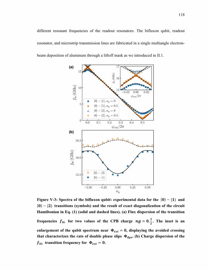
118
different resonant frequencies of the readout resonators. The bifluxon qubit, readout
resonator, and microstrip transmission lines are fabricated in a single multiangle electron-
beam deposition of aluminum through a liftoff mask as we introduced in II.1.
Figure V-3: Spectra of the bifluxon qubit: experimental data for the |⟩ − |⟩ and
|⟩ − |⟩ transitions (symbols) and the result of exact diagonalization of the circuit
Hamiltonian in Eq. (1) (solid and dashed lines). (a) Flux dispersion of the transition
frequencies for two values of the CPB charge = ,
. The inset is an
enlargement of the qubit spectrum near = , displaying the avoided crossing
that characterizes the rate of double phase slips . (b) Charge dispersion of the
transition frequency for = .
119
The pump tone induces the |0⟩ − |⟩ transitions at the resonance frequencies
= ( − )/ℎ. The measurement tone probes the dispersive shift of the coupled
readout resonator. Although the dispersive measurements in the protected regime are
complicated by significantly reduced qubit-readout coupling, the signal-to-noise ratio in
the spectroscopic measurements is sufficiently high to identify the resonances even in the
protected regime. The flux dependencies of the resonance frequencies () and
at = 0,
are shown in Figure V-3(a). The obtained spectra are in good
agreement with the results of diagonalization of the circuit Hamiltonian [solid lines in
Figure V-3(a)], with fitting parameters /ℎ = 27.2GHz , /ℎ = 7.7GHz , /ℎ =
0.94GHz, and /ℎ = 10GHz, and asymmetry between the CPB junctions Δ ≡ −
= ℎ × 6GHz.
The extracted values are consistent with the expected JJ parameters. The normal-
state resistance of the CPB junctions extracted from using the Ambegaokar-Baratoff
relation agrees within 20% with the normal state resistance of test junctions
fabricated on the same chip. Both CPB and SI charging energies agree well with the typical
aluminum-based junction capacitance 50fF/μm and specific capacitance of micron-size
islands on silicon substrates 0.085fF/μm [132].

120
We also observe an additional resonance at 13.9GHz, whose position does not
depend on and . We attribute this resonance to the lowest-frequency mode of the
superinductor, which corresponds to characteristic impedance of the SI = 14Ω.
Figure V-4: (a) Measurements of the bifluxon energy relaxation in the protected state
(red circles) and unprotected state (blue squares). The sequence of pulses is shown in
the inset. The exponential fits are shown by solid and dashed lines, respectively. Note
that the resonance energy of the qubit in the protected
state is × . (approximately × ), and a nonzero occupancy of the
first excited state [( ⁄ ) + ]⁄ with the qubit temperature = =
is taken into account. (b) Demonstration of an absence of qubit excitation by
the gate voltage pulses.
121
V.5 Time-domain analysis
In the time-domain experiments the signal-to-noise ratio, reduced by weak qubit-
readout coupling, is too low to employ conventional pulse protocols (decay, Rabi
oscillations, and Ramsey fringes). For this reason, we designed special pulse sequences for
and measurements in the protected regime. The pulse sequence used for probing
the decay is shown in Figure V-4(a). Initially the qubit is prepared in the ground
unprotected state ( = 0). A microwave pulse at the resonant frequency ()
excited
the qubit, and then the protection is turned on by applying a pulse of the gate voltage
corresponding to the offset charge =
. We have used pulses with the rise and drop
times approximately 30ns ≫ 1/(()
− ( ⁄ )
)) , which is sufficiently long to ensure
adiabatic evolution of the qubit between protected and unprotected states. After time Δ,
the protection is removed by setting = 0 and the qubit state is measured. As a control
experiment, we apply the gate voltage pulses alone, without a pulse; the absence of
qubit excitation proved the adiabaticity of gate manipulations; see Figure V-4(b).
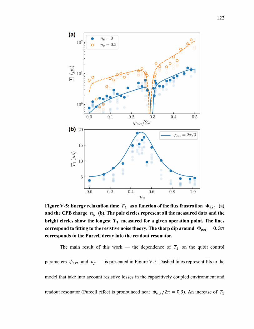
122
Figure V-5: Energy relaxation time as a function of the flux frustration (a)
and the CPB charge (b). The pale circles represent all the measured data and the
bright circles show the longest measured for a given operation point. The lines
correspond to fitting to the resistive noise theory. The sharp dip around = .
corresponds to the Purcell decay into the readout resonator.
The main result of this work — the dependence of on the qubit control
parameters and — is presented in Figure V-5. Dashed lines represent fits to the
model that take into account resistive losses in the capacitively coupled environment and
readout resonator (Purcell effect is pronounced near /2 = 0.3). An increase of

123
in the protected regime by an order of magnitude provides evidence for the qubit’s dipole
moment suppression. The longest decay time of greater than 100 is measured at full
flux frustration = , which corresponds to a minimum qubit energy ( ⁄ )
=
0.4GHz.
Direct measurements of the decoherence time in the protected regime, by either
Rabi or Ramsey techniques, are not feasible because of vanishing coupling of the qubit o
microwave pulses. For this reason, we modified the measurements of Ramsey fringes by
analogy with the aforementioned measurements. The pulse sequence is shown in
Figure V-6(a). Both 30ns long /2 microwave pulses detuned from the qubit transition
frequency by 4MHz are applied in the unprotected state ( = 0 ), and the qubit is
measured after the end of the second pulse. Between the /2 pulses, while the qubit
undergoes free precession, the qubit’s protected state is restored by applying a gate voltage
pulse ( = 1 2⁄ ). After averaging over 1000 cycles, the Ramsey fringes are recorded by
varying the delay between the end of the gate pulse and the second /2 pulse.
Ramsey fringes measured according to this procedure for one of the flux “sweet
spots” at = 0 are shown in Figure V-6(b); the pulse for these measurements
is 0.27μs ong. The difference between the amplitudes of Ramsey ringes at moments Δ =
0 and 0.27μs may provide information on dephasing in the protected state if this is the

124
only source of dephasing. However, the accuracy of this technique is limited by the
pulse jitter. Indeed, in the rotating frame of the unprotected state, the qubit’s state vector
rotates in the equatorial plane of the Bloch sphere as soon as the protection is turned on.
The angular velocity of these rotations, = ()
− ( ⁄ )
ℏ⁄ , is large ( > 2 × 1GHz)
at both flux sweet spots = 0, ; and even a small jitter can result in a significant error
in the position of the qubit’s state vector at the end of the pulse. According to the
specification, the jitter time of the pulse generator used in our experiments could be as large
as 0.3ns. This jitter-induced phase uncertainty alone, without invoking any dephasing in
the protected state, is sufficient to explain the reduced amplitude of Ramsey fringes at
Δ = 0.28μs. Thus, these measurements can impose only the lower limit on , which is
close to 1μs for the data in Figure V-6(b). Future experiments with better controlled
pulses of different lengths may provide more detailed information on at both sweet
spots.
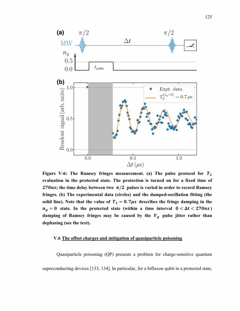
125
Figure V-6: The Ramsey fringes measurement. (a) The pulse protocol for
evaluation in the protected state. The protection is turned on for a fixed time of
; the time delay between two / pulses is varied in order to record Ramsey
fringes. (b) The experimental data (circles) and the damped-oscillation fitting (the
solid line). Note that the value of = . describes the fringe damping in the
= state. In the protected state (within a time interval < < )
damping of Ramsey fringes may be caused by the pulse jitter rather than
dephasing (see the text).
V.6 The offset charges and mitigation of quasiparticle poisoning
Quasiparticle poisoning (QP) presents a problem for charge-sensitive quantum
superconducting devices [133, 134]. In particular, for a bifluxon qubit in a protected state,

126
tunneling of a nonequilibrium quasiparticle into or out of the CPB island would remove
protection. To minimize QP, we use so-called gap engineering [135, 136].
In Figure V-7(a) we show the superconducting gap in the CPB island and the outer
electrodes that form the CPB Josephson junctions. Because of the dependence of the
critical temperature of films on their thickness, the gap in the thin (20 ) CPB island
is greater than that in thicker (60 ) outer electrodes. This difference , which we
estimate to be approximately (0.3 ÷ 0.4) (see [137]), is sufficiently large to block
tunneling of nonequilibrium quasiparticles with energies greater than onto the CPB
island at sufficiently low temperatures. The efficiency of this technique is demonstrated in
Figure V-7(b) to Figure V-7(d). If both the CPB island and outer electrodes are thick (Δ ≈
0), we observe a characteristic “eye” pattern [135] in the spectroscopic measurements,
which reflects rapid ± jumps of the CPB charge on the timescale of a single scan of the
resonance of the readout resonator; see Figure V-7(b). This pattern vanishes if the gap
engineering is employed and reappears only at higher temperatures, where the
quasiparticles are thermally excited in the CPB island (compare panels (c) and (d) of Figure
V-7). Gap engineering and careful infrared and magnetic shielding of the device allow us
to increase the time intervals between the QP events up to 30mins. In Figure V-7(e) we
show that, in addition to rare QP events, in the gap-engineered device we observe slow
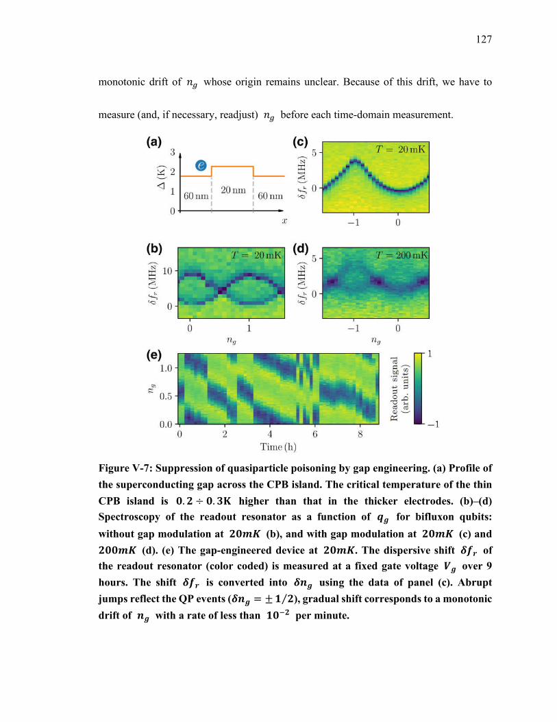
127
monotonic drift of whose origin remains unclear. Because of this drift, we have to
measure (and, if necessary, readjust) before each time-domain measurement.
Figure V-7: Suppression of quasiparticle poisoning by gap engineering. (a) Profile of
the superconducting gap across the CPB island. The critical temperature of the thin
CPB island is . ÷ . higher than that in the thicker electrodes. (b)–(d)
Spectroscopy of the readout resonator as a function of for bifluxon qubits:
without gap modulation at (b), and with gap modulation at (c) and
(d). (e) The gap-engineered device at . The dispersive shift of
the readout resonator (color coded) is measured at a fixed gate voltage over 9
hours. The shift is converted into using the data of panel (c). Abrupt
jumps reflect the QP events ( = ± ⁄ ), gradual shift corresponds to a monotonic
drift of with a rate of less than per minute.
128
V.7 Conclusion
In this work, we develop and characterize a symmetry-protected superconducting
qubit that offers simultaneous exponential suppression of energy decay from charge and
flux noises, and dephasing from flux noise. Provided the offset charge on the CPB island
is an odd number of electrons, the qubit potential corresponds to that of a (/2)
Josephson element, preserving the parity of fluxons in the loop via Aharonov-Casher
interference. In this regime, the logical-state wavefunctions reside in disjoint regions of
Hilbert space, thereby ensuring protection against energy decay. By switching the
protection on, we observe a tenfold increase of the decay time, reaching up to 100 .
Though the qubit is sensitive to charge noise, the sensitivity is much reduced in comparison
with the charge qubit, and the charge-noise-induced dephasing time of the current device
exceeds 1 . Implementation of full dephasing protection can be achieved in the next-
generation devices by combining several (/2) Josephson elements in a small array.

129
CONCLUSION AND OUTLOOK
In this work we developed and characterized quantum superconducting circuits that
serves as a platform for the realization of protected qubits with simultaneous exponential
suppression of energy decay from charge and flux noise. This chapter summarizes the
results and provides outlook for future work.
VI.1 Junctions with low Josephson energy
In Chapter III, we address the transition to a dissipative transport in low-
junctions driven by the incoherent phase slips. We observed that the switching current,
which corresponds to an abrupt increase of the voltage across the JJ to V = 2Δ ⁄ and
generation of quasiparticles, is strongly reduced in such junctions with respect to the
Ambegaokar-Baratoff’s prediction for the critical current. The premature switching ≪
; is accompanied by an increase of the zero-bias resistance . We attributed this
behavior to the temperature activated phase slips whose rate exponentially increases with
decreasing .The dissipation associated with TAPS might limit the performance of qubits
based on low- junctions [13, 14, 36]. Steep temperature dependence of the coherence
time at temperatures could be a signature of TAPS-induced decoherence. This

130
dependence, observed in the experiments with the “heavy” fluxonium [87], requires further
investigations.
VI.2 Superinductors based on granular aluminum thin films
In Chapter IV, we fabricated and characterized CPW half wavelength resonators
made of strongly disordered films. Due to a very high kinetic inductance of these
films, we were able to significantly reduce the footprint of the CPW resonators from
size down to tens of . We realized a superinductor with impedance ≈ 5Ω
approaching the resistance quantum . High kinetic inductance in combination with low
microwave losses make films promising for a wide range of microwave applications
which include kinetic inductance photon detectors and superconducting quantum circuits.
In a more recent work [19], by meandering the nanowires, we were able to fabricate
several lumped-element superinductors with impedance 10 ÷ 30Ω and
inductance 0.1 ÷ 1.3.
To fabricate films reliably, further material characterization is required. One
of the common concerns in fabricating thin films is that disorder and grain
connectivity are not well controlled, which underscores the need for better control of the
critical film formation parameters. Another promising direction of research is the use of

131
for mitigating the quasiparticle poisoning as demonstrated in Chapter V. By
introducing disorder in Al films (Figure II-6), it is possible to increase from 1.3 to
2. Such enhancement opens possibilities for suppression of quasiparticle poisoning by
for gap engineering. Wea re currently working on fabricating the quasiparticle barriers by
in-situ modification of the structure of Al films with the focus ion beam technology.
VI.3 Fluxon-parity protected qubits
In Chapter V we developed and characterized a symmetry-protected
superconducting qubit that offers simultaneous exponential suppression of energy decay
from charge and flux noises, and dephasing from flux noise. The qubit consists of a Cooper-
pair box (CPB) shunted by a superinductor, forming a superconducting loop. Provided the
offset charge on the CPB island is an odd number of electrons, the qubit potential
corresponds to that of a cos (/2) Josephson element, preserving the parity of fluxons in
the loop via Aharonov-Casher interference. In this regime, the logic-state wavefunctions
reside in disjoint regions of phase space, thereby ensuring the protection against energy
decay. By switching the protection on, we observed a ten-fold increase of the decay time,
reaching up to 100 s. Though the qubit is sensitive to charge noise, the sensitivity is much
reduced in comparison with the charge qubit, and the charge-noise-induced dephasing time

132
of the current device exceeds 1 s. Implementation of the full dephasing protection can be
achieved in the next-generation devices by combining several cos( /2 ) Josephson
elements in a small array.
Ideally the lowest-energy states of a fully symmetric bifluxon are exactly
degenerate at /2 = = 1 2⁄ . However, slight deviations from this point would
open a gap in the spectrum and lead to decoherence. As being discussed in [14], in order
to mitigate dephasing due to both charge and flux noises, one strategy could be to combine
an increase of / with strong reduction of the inductive energy . As we mentioned
in Chapter V, an exponentially small flux dispersion can be achieved in the regime ≫
2 . Fulfilling this condition requires the implementation of an ultrahigh-impedance
superconductor with > 30μH and self-resonance frequencies greater than 1GHz. It is
therefore a primary interest in the future to pursue superinductors with even greater
presented in -based superinductors as in [19].
133
REFERENCES
[1] J. M. Martinis, M. H. Devoret, and J. Clarke, "Energy-Level Quantization in the
Zero-Voltage State of a Current-Biased Josephson Junction," Physical Review
Letters, vol. 55, no. 15, pp. 1543-1546, 10/07/ 1985, doi:
10.1103/PhysRevLett.55.1543.
[2] J. M. Martinis, M. H. Devoret, and J. Clarke, "Quantum Josephson junction circuits
and the dawn of artificial atoms," Nature Physics, vol. 16, no. 3, pp. 234-237,
2020/03/01 2020, doi: 10.1038/s41567-020-0829-5.
[3] C. Macklin et al., "A near–quantum-limited Josephson traveling-wave parametric
amplifier," Science, vol. 350, no. 6258, p. 307, 2015, doi: 10.1126/science.aaa8525.
[4] M. Kjaergaard et al., "Superconducting Qubits: Current State of Play," Annual
Review of Condensed Matter Physics, vol. 11, no. 1, pp. 369-395, 2020/03/10 2020,
doi: 10.1146/annurev-conmatphys-031119-050605.
[5] J. Koch et al., "Charge-insensitive qubit design derived from the Cooper pair box,"
Physical Review A, vol. 76, no. 4, p. 042319, 10/12/ 2007, doi:
10.1103/PhysRevA.76.042319.
[6] F. Arute et al., "Quantum supremacy using a programmable superconducting
processor," Nature, vol. 574, no. 7779, pp. 505-510, 2019/10/01 2019, doi:
10.1038/s41586-019-1666-5.
[7] J. M. Chow et al., "Universal Quantum Gate Set Approaching Fault-Tolerant
Thresholds with Superconducting Qubits," Physical Review Letters, vol. 109, no.
6, p. 060501, 08/09/ 2012, doi: 10.1103/PhysRevLett.109.060501.
[8] F. Motzoi, J. M. Gambetta, P. Rebentrost, and F. K. Wilhelm, "Simple Pulses for
Elimination of Leakage in Weakly Nonlinear Qubits," Physical Review Letters, vol.
103, no. 11, p. 110501, 09/08/ 2009, doi: 10.1103/PhysRevLett.103.110501.
[9] J. M. Chow et al., "Optimized driving of superconducting artificial atoms for
improved single-qubit gates," Physical Review A, vol. 82, no. 4, p. 040305, 10/27/
2010, doi: 10.1103/PhysRevA.82.040305.
[10] Y. Shalibo et al., "Lifetime and Coherence of Two-Level Defects in a Josephson
Junction," Physical Review Letters, vol. 105, no. 17, p. 177001, 10/19/ 2010, doi:
10.1103/PhysRevLett.105.177001.
[11] C. Müller, J. H. Cole, and J. Lisenfeld, "Towards understanding two-level-systems
in amorphous solids: insights from quantum circuits," Reports on Progress in
Physics, vol. 82, no. 12, p. 124501, 2019/10/30 2019, doi: 10.1088/1361-
6633/ab3a7e.
134
[12] J. M. Sage, V. Bolkhovsky, W. D. Oliver, B. Turek, and P. B. Welander, "Study of
loss in superconducting coplanar waveguide resonators," Journal of Applied
Physics, vol. 109, no. 6, p. 063915, 2011/03/15 2011, doi: 10.1063/1.3552890.
[13] W. C. Smith, A. Kou, X. Xiao, U. Vool, and M. H. Devoret, "Superconducting
circuit protected by two-Cooper-pair tunneling," npj Quantum Information, vol. 6,
no. 1, p. 8, 2020/01/21 2020, doi: 10.1038/s41534-019-0231-2.
[14] K. Kalashnikov et al., "Bifluxon: Fluxon-Parity-Protected Superconducting Qubit,"
PRX Quantum, vol. 1, no. 1, p. 010307, 09/03/ 2020, doi:
10.1103/PRXQuantum.1.010307.
[15] M. T. Bell, I. A. Sadovskyy, L. B. Ioffe, A. Y. Kitaev, and M. E. Gershenson,
"Quantum Superinductor with Tunable Nonlinearity," Physical Review Letters, vol.
109, no. 13, p. 137003, 09/27/ 2012, doi: 10.1103/PhysRevLett.109.137003.
[16] M. T. Bell, J. Paramanandam, L. B. Ioffe, and M. E. Gershenson, "Protected
Josephson Rhombus Chains," Physical Review Letters, vol. 112, no. 16, p. 167001,
04/25/ 2014, doi: 10.1103/PhysRevLett.112.167001.
[17] M. T. Bell, W. Zhang, L. B. Ioffe, and M. E. Gershenson, "Spectroscopic Evidence
of the Aharonov-Casher Effect in a Cooper Pair Box," Physical Review Letters, vol.
116, no. 10, p. 107002, 03/10/ 2016, doi: 10.1103/PhysRevLett.116.107002.
[18] W. Zhang, K. Kalashnikov, W.-S. Lu, P. Kamenov, T. DiNapoli, and M. E.
Gershenson, "Microresonators Fabricated from High-Kinetic-Inductance
Aluminum Films," Physical Review Applied, vol. 11, no. 1, p. 011003, 01/11/ 2019,
doi: 10.1103/PhysRevApplied.11.011003.
[19] P. Kamenov, W.-S. Lu, K. Kalashnikov, T. DiNapoli, M. T. Bell, and M. E.
Gershenson, "Granular Aluminum Meandered Superinductors for Quantum
Circuits," Physical Review Applied, vol. 13, no. 5, p. 054051, 05/20/ 2020, doi:
10.1103/PhysRevApplied.13.054051.
[20] B. D. Josephson, "Possible new effects in superconductive tunnelling," Physics
Letters, vol. 1, no. 7, pp. 251-253, 1962/07/01/ 1962, doi:
https://doi.org/10.1016/0031-9163(62)91369-0.
[21] V. Ambegaokar and A. Baratoff, "Tunneling Between Superconductors," Physical
Review Letters, vol. 10, no. 11, pp. 486-489, 06/01/ 1963, doi:
10.1103/PhysRevLett.10.486.
[22] D. E. McCumber, "Effect of ac Impedance on dc Voltage‐Current Characteristics
of Superconductor Weak‐Link Junctions," Journal of Applied Physics, vol. 39, no.
7, pp. 3113-3118, 1968/06/01 1968, doi: 10.1063/1.1656743.
[23] D. F. S. D. J. Griffiths, Introduction to Quantum Mechanics. 2019.

135
[24] J. M. Kivioja, T. E. Nieminen, J. Claudon, O. Buisson, F. W. J. Hekking, and J. P.
Pekola, "Observation of Transition from Escape Dynamics to Underdamped Phase
Diffusion in a Josephson Junction," Physical Review Letters, vol. 94, no. 24, p.
247002, 06/22/ 2005, doi: 10.1103/PhysRevLett.94.247002.
[25] G. Rastelli, I. M. Pop, and F. W. J. Hekking, "Quantum phase slips in Josephson
junction rings," Physical Review B, vol. 87, no. 17, p. 174513, 05/16/ 2013, doi:
10.1103/PhysRevB.87.174513.
[26] M. H. Devoret, J. M. Martinis, and J. Clarke, "Measurements of Macroscopic
Quantum Tunneling out of the Zero-Voltage State of a Current-Biased Josephson
Junction," Physical Review Letters, vol. 55, no. 18, pp. 1908-1911, 10/28/ 1985,
doi: 10.1103/PhysRevLett.55.1908.
[27] R. C. Jaklevic, J. Lambe, A. H. Silver, and J. E. Mercereau, "Quantum Interference
Effects in Josephson Tunneling," Physical Review Letters, vol. 12, no. 7, pp. 159-
160, 02/17/ 1964, doi: 10.1103/PhysRevLett.12.159.
[28] M. Tinkham, Introduction to Superconductivity. Dover Publications, 2004.
[29] K. Nakajima, Y. Onodera, and Y. Ogawa, "Logic design of Josephson network,"
Journal of Applied Physics, vol. 47, no. 4, pp. 1620-1627, 1976/04/01 1976, doi:
10.1063/1.322782.
[30] J. P. Hurrell and A. H. Silver, "SQUID digital electronics," AIP Conference
Proceedings, vol. 44, no. 1, pp. 437-447, 1978/07/01 1978, doi: 10.1063/1.31377.
[31] K. K. Likharev, "Superconductor digital electronics," Physica C: Superconductivity
and its Applications, vol. 482, pp. 6-18, 2012/11/20/ 2012, doi:
https://doi.org/10.1016/j.physc.2012.05.016.
[32] W. Chen, A. V. Rylyakov, V. Patel, J. E. Lukens, and K. K. Likharev, "Rapid single
flux quantum T-flip flop operating up to 770 GHz," IEEE Transactions on Applied
Superconductivity, vol. 9, no. 2, pp. 3212-3215, 1999, doi: 10.1109/77.783712.
[33] P. Bunyk, K. Likharev, and D. Zinoviev, "RSFQ TECHNOLOGY: PHYSICS
AND DEVICES," International Journal of High Speed Electronics and Systems,
vol. 11, no. 01, pp. 257-305, 2001/03/01 2001, doi: 10.1142/S012915640100085X.
[34] V. Bouchiat, D. Vion, P. Joyez, D. Esteve, and M. H. Devoret, "Quantum
Coherence with a Single Cooper Pair," Physica Scripta, vol. T76, no. 1, p. 165,
1998, doi: 10.1238/physica.topical.076a00165.
[35] A. W. M. H. Devoret, J. M. Martinis, "Superconducting Qubits: A Short Review,"
2004, doi: arXiv:cond-mat/0411174.
136
[36] L. B. Nguyen, Y.-H. Lin, A. Somoroff, R. Mencia, N. Grabon, and V. E.
Manucharyan, "High-Coherence Fluxonium Qubit," Physical Review X, vol. 9, no.
4, p. 041041, 11/25/ 2019, doi: 10.1103/PhysRevX.9.041041.
[37] J. M. Martinis and R. L. Kautz, "Classical phase diffusion in small hysteretic
Josephson junctions," Physical Review Letters, vol. 63, no. 14, pp. 1507-1510,
10/02/ 1989, doi: 10.1103/PhysRevLett.63.1507.
[38] M. Peruzzo, A. Trioni, F. Hassani, M. Zemlicka, and J. M. Fink, "Surpassing the
Resistance Quantum with a Geometric Superinductor," Physical Review Applied,
vol. 14, no. 4, p. 044055, 10/29/ 2020, doi: 10.1103/PhysRevApplied.14.044055.
[39] J. Zmuidzinas, "Superconducting Microresonators: Physics and Applications,"
Annual Review of Condensed Matter Physics, vol. 3, no. 1, pp. 169-214, 2012, doi:
10.1146/annurev-conmatphys-020911-125022.
[40] D. Niepce, J. Burnett, and J. Bylander, "High Kinetic Inductance
$\mathrmNb\mathrmN$ Nanowire Superinductors," Physical Review Applied,
vol. 11, no. 4, p. 044014, 04/04/ 2019, doi: 10.1103/PhysRevApplied.11.044014.
[41] P. C. J. J. Coumou, E. F. C. Driessen, J. Bueno, C. Chapelier, and T. M. Klapwijk,
"Electrodynamic response and local tunneling spectroscopy of strongly disordered
superconducting TiN films," Physical Review B, vol. 88, no. 18, p. 180505, 11/07/
2013, doi: 10.1103/PhysRevB.88.180505.
[42] O. Dupré et al., "Tunable sub-gap radiation detection with superconducting
resonators," Superconductor Science and Technology, vol. 30, no. 4, p. 045007,
2017/02/24 2017, doi: 10.1088/1361-6668/aa5b14.
[43] S. E. de Graaf et al., "Charge quantum interference device," Nature Physics, vol.
14, no. 6, pp. 590-594, 2018/06/01 2018, doi: 10.1038/s41567-018-0097-9.
[44] H. Rotzinger et al., "Aluminium-oxide wires for superconducting high kinetic
inductance circuits," Superconductor Science and Technology, vol. 30, no. 2, p.
025002, 2016/11/30 2016, doi: 10.1088/0953-2048/30/2/025002.
[45] J. Luomahaara, V. Vesterinen, L. Grönberg, and J. Hassel, "Kinetic inductance
magnetometer," Nature Communications, vol. 5, no. 1, p. 4872, 2014/09/10 2014,
doi: 10.1038/ncomms5872.
[46] M. A. Wolff et al., "Waveguide-Integrated Superconducting Nanowire
SinglePhoton Detector Array for Ultra-Fast Quantum Key Distribution," in
Conference on Lasers and Electro-Optics, Washington, DC, 2020/05/10 2020:
Optical Society of America, in OSA Technical Digest, p. SM4O.5, doi:
10.1364/CLEO_SI.2020.SM4O.5. [Online]. Available:
http://www.osapublishing.org/abstract.cfm?URI=CLEO_SI-2020-SM4O.5

137
[47] M. V. Feigel’man and L. B. Ioffe, "Microwave Properties of Superconductors Close
to the Superconductor-Insulator Transition," Physical Review Letters, vol. 120, no.
3, p. 037004, 01/19/ 2018, doi: 10.1103/PhysRevLett.120.037004.
[48] W. Zhang, W. Huang, M. E. Gershenson, and M. T. Bell, "Josephson Metamaterial
with a Widely Tunable Positive or Negative Kerr Constant," Physical Review
Applied, vol. 8, no. 5, p. 051001, 11/13/ 2017, doi:
10.1103/PhysRevApplied.8.051001.
[49] N. A. Masluk, I. M. Pop, A. Kamal, Z. K. Minev, and M. H. Devoret, "Microwave
Characterization of Josephson Junction Arrays: Implementing a Low Loss
Superinductance," Physical Review Letters, vol. 109, no. 13, p. 137002, 09/27/
2012, doi: 10.1103/PhysRevLett.109.137002.
[50] V. E. Manucharyan, "Superinductor," Yale University, 2012.
[51] R. Vijay, M. H. Devoret, and I. Siddiqi, "Invited Review Article: The Josephson
bifurcation amplifier," Review of Scientific Instruments, vol. 80, no. 11, p. 111101,
2009/11/01 2009, doi: 10.1063/1.3224703.
[52] Y. S. Fei Yan, Philip Krantz, Archana Kamal, David K. Kim, Jonilyn L. Yoder,
Terry P. Orlando, Simon Gustavsson, William D. Oliver, "Engineering Framework
for Optimizing Superconducting Qubit Designs," 2020, doi: arXiv:2006.04130.
[53] P. Groszkowski et al., "Coherence properties of the 0-πqubit," New Journal of
Physics, vol. 20, no. 4, p. 043053, 2018/04/25 2018, doi: 10.1088/1367-
2630/aab7cd.
[54] I. M. Pop et al., "Measurement of the effect of quantum phase slips in a Josephson
junction chain," Nature Physics, vol. 6, no. 8, pp. 589-592, 2010/08/01 2010, doi:
10.1038/nphys1697.
[55] I. V. Pechenezhskiy, R. A. Mencia, L. B. Nguyen, Y.-H. Lin, and V. E.
Manucharyan, "The superconducting quasicharge qubit," Nature, vol. 585, no.
7825, pp. 368-371, 2020/09/01 2020, doi: 10.1038/s41586-020-2687-9.
[56] A. Kitaev, "Protected qubit based on a superconducting current mirror," 2006, doi:
arXiv:cond-mat/0609441.
[57] B. Douçot and L. B. Ioffe, "Voltage-current curves for small Josephson junction
arrays: Semiclassical treatment," Physical Review B, vol. 76, no. 21, p. 214507,
12/18/ 2007, doi: 10.1103/PhysRevB.76.214507.
[58] B. Douçot and L. B. Ioffe, "Physical implementation of protected qubits," Reports
on Progress in Physics, vol. 75, no. 7, p. 072001, 2012/06/28 2012, doi:
10.1088/0034-4885/75/7/072001.

138
[59] L. Grünhaupt et al., "Granular aluminium as a superconducting material for high-
impedance quantum circuits," Nature Materials, vol. 18, no. 8, pp. 816-819,
2019/08/01 2019, doi: 10.1038/s41563-019-0350-3.
[60] W. Zhang, "Applications of superinductors in superconducting quantum circuits,"
(in English), 2019, doi: https://doi.org/doi:10.7282/t3-3g4k-wt20.
[61] J. M. Kreikebaum, K. P. O’Brien, A. Morvan, and I. Siddiqi, "Improving wafer-
scale Josephson junction resistance variation in superconducting quantum coherent
circuits," Superconductor Science and Technology, vol. 33, no. 6, p. 06LT02,
2020/05/05 2020, doi: 10.1088/1361-6668/ab8617.
[62] U. S. Pracht et al., "Enhanced Cooper pairing versus suppressed phase coherence
shaping the superconducting dome in coupled aluminum nanograins," Physical
Review B, vol. 93, no. 10, p. 100503, 03/21/ 2016, doi:
10.1103/PhysRevB.93.100503.
[63] J. Paramanandam, "Classical and quantum properties of variable-coordination
number Josephson junction arrays," (in eng), 2015, doi:
https://doi.org/doi:10.7282/T3CR5WB7.
[64] S. Schmidlin, "Physics and Technology of small Josephson junctions," Doctoral
Thesis, 2013.
[65] L. S. Kuzmin, Y. V. Nazarov, D. B. Haviland, P. Delsing, and T. Claeson,
"Coulomb blockade and incoherent tunneling of Cooper pairs in ultrasmall
junctions affected by strong quantum fluctuations," Physical Review Letters, vol.
67, no. 9, pp. 1161-1164, 08/26/ 1991, doi: 10.1103/PhysRevLett.67.1161.
[66] M. T. Bell, L. B. Ioffe, and M. E. Gershenson, "Microwave spectroscopy of a
Cooper-pair transistor coupled to a lumped-element resonator," Physical Review B,
vol. 86, no. 14, p. 144512, 10/11/ 2012, doi: 10.1103/PhysRevB.86.144512.
[67] Q. F. Aaron Somoroff, Raymond A. Mencia, Haonan Xiong, Roman V. Kuzmin,
Vladimir E. Manucharyan, "Millisecond coherence in a superconducting qubit,"
2021, doi: arXiv:2103.08578.
[68] K. A. Matveev, A. I. Larkin, and L. I. Glazman, "Persistent Current in
Superconducting Nanorings," Physical Review Letters, vol. 89, no. 9, p. 096802,
08/08/ 2002, doi: 10.1103/PhysRevLett.89.096802.
[69] J. D. Teufel, "Superconducting tunnel junctions as direct detectors for
submillimeter astronomy," 2008. [Online]. Available:
https://ui.adsabs.harvard.edu/abs/2008PhDT........46T
[70] M. Cirillo, I. Modena, F. Santucci, P. Carelli, M. G. Castellano, and R. Leoni,
"Radiation detection from Fiske steps in Josephson junctions above 200 GHz,"
139
Journal of Applied Physics, vol. 73, no. 12, pp. 8637-8640, 1993/06/15 1993, doi:
10.1063/1.353396.
[71] D. D. Coon and M. D. Fiske, "Josephson ac and Step Structure in the Supercurrent
Tunneling Characteristic," Physical Review, vol. 138, no. 3A, pp. A744-A746,
05/03/ 1965, doi: 10.1103/PhysRev.138.A744.
[72] Y. M. Ivanchenko and L. Zil'berman, "The Josephson Effect in Small Tunnel
Contacts," Journal of Experimental and Theoretical Physics, 1969.
[73] J. B. Johnson, "Thermal Agitation of Electricity in Conductors," Physical Review,
vol. 32, no. 1, pp. 97-109, 07/01/ 1928, doi: 10.1103/PhysRev.32.97.
[74] B. Jäck, J. Senkpiel, M. Etzkorn, J. Ankerhold, C. R. Ast, and K. Kern, "Quantum
Brownian Motion at Strong Dissipation Probed by Superconducting Tunnel
Junctions," Physical Review Letters, vol. 119, no. 14, p. 147702, 10/04/ 2017, doi:
10.1103/PhysRevLett.119.147702.
[75] H. Shimada, S. Katori, S. Gandrothula, T. Deguchi, and Y. Mizugaki, "Bloch
Oscillation in a One-Dimensional Array of Small Josephson Junctions," Journal of
the Physical Society of Japan, vol. 85, no. 7, p. 074706, 2016/07/15 2016, doi:
10.7566/JPSJ.85.074706.
[76] M. Iansiti, A. T. Johnson, C. J. Lobb, and M. Tinkham, "Crossover from Josephson
Tunneling to the Coulomb Blockade in Small Tunnel Junctions," Physical Review
Letters, vol. 60, no. 23, pp. 2414-2417, 06/06/ 1988, doi:
10.1103/PhysRevLett.60.2414.
[77] T. Weißl et al., "Bloch band dynamics of a Josephson junction in an inductive
environment," Physical Review B, vol. 91, no. 1, p. 014507, 01/15/ 2015, doi:
10.1103/PhysRevB.91.014507.
[78] E. Chow, P. Delsing, and D. B. Haviland, "Length-Scale Dependence of the
Superconductor-to-Insulator Quantum Phase Transition in One Dimension,"
Physical Review Letters, vol. 81, no. 1, pp. 204-207, 07/06/ 1998, doi:
10.1103/PhysRevLett.81.204.
[79] J. S. Penttilä, P. J. Hakonen, E. B. Sonin, and M. A. Paalanen, "Experiments on
Dissipative Dynamics of Single Josephson Junctions," Journal of Low Temperature
Physics, vol. 125, no. 3, pp. 89-114, 2001/11/01 2001, doi:
10.1023/A:1012971500694.
[80] R. L. Kautz and J. M. Martinis, "Noise-affected I-V curves in small hysteretic
Josephson junctions," Physical Review B, vol. 42, no. 16, pp. 9903-9937, 12/01/
1990, doi: 10.1103/PhysRevB.42.9903.

140
[81] S.-S. Yeh et al., "A method for determining the specific capacitance value of
mesoscopic Josephson junctions," Applied Physics Letters, vol. 101, no. 23, p.
232602, 2012/12/03 2012, doi: 10.1063/1.4769999.
[82] R. Ono, M. Cromar, R. Kautz, R. Soulen, J. Colwell, and W. Fogle, "Current-
voltage characteristics of nanoampere Josephson junctions," IEEE Transactions on
Magnetics, vol. 23, no. 2, pp. 1670-1673, 1987, doi: 10.1109/TMAG.1987.1064932.
[83] D. B. Haviland, K. Andersson, P. Ågren, J. Johansson, V. Schöllmann, and M.
Watanabe, "Quantum phase transition in one-dimensional Josephson junction
arrays," Physica C: Superconductivity, vol. 352, no. 1, pp. 55-60, 2001/04/01/ 2001,
doi: https://doi.org/10.1016/S0921-4534(00)01675-0.
[84] H. Akoh, O. Liengme, M. Iansiti, M. Tinkham, and J. U. Free, "Reentrant
temperature dependence of the critical current in small tunnel junctions," Physical
Review B, vol. 33, no. 3, pp. 2038-2041, 02/01/ 1986, doi:
10.1103/PhysRevB.33.2038.
[85] Y. Yoon, S. Gasparinetti, M. Möttönen, and J. P. Pekola, "Capacitively Enhanced
Thermal Escape in Underdamped Josephson Junctions," Journal of Low
Temperature Physics, vol. 163, no. 3, pp. 164-169, 2011/05/01 2011, doi:
10.1007/s10909-011-0344-2.
[86] M. Watanabe and D. B. Haviland, "Quantum phase transition and Coulomb
blockade with one-dimensional SQUID arrays," Journal of Physics and Chemistry
of Solids, vol. 63, no. 6, pp. 1307-1310, 2002/06/01/ 2002, doi:
https://doi.org/10.1016/S0022-3697(02)00040-9.
[87] "private communication, Manucharyan, Vladimir E.," ed, 2020.
[88] M. H. Devoret and R. J. Schoelkopf, "Superconducting Circuits for Quantum
Information: An Outlook," Science, vol. 339, no. 6124, pp. 1169-1174, 2013, doi:
10.1126/science.1231930.
[89] H. Paik et al., "Observation of High Coherence in Josephson Junction Qubits
Measured in a Three-Dimensional Circuit QED Architecture," Physical Review
Letters, vol. 107, no. 24, p. 240501, 12/05/ 2011, doi:
10.1103/PhysRevLett.107.240501.
[90] R. Barends et al., "Coherent Josephson Qubit Suitable for Scalable Quantum
Integrated Circuits," Physical Review Letters, vol. 111, no. 8, p. 080502, 08/22/
2013, doi: 10.1103/PhysRevLett.111.080502.
[91] D. C. Mattis and J. Bardeen, "Theory of the Anomalous Skin Effect in Normal and
Superconducting Metals," Physical Review, vol. 111, no. 2, pp. 412-417, 07/15/
1958, doi: 10.1103/PhysRev.111.412.

141
[92] M. Swanson, Y. L. Loh, M. Randeria, and N. Trivedi, "Dynamical Conductivity
across the Disorder-Tuned Superconductor-Insulator Transition," Physical Review
X, vol. 4, no. 2, p. 021007, 04/09/ 2014, doi: 10.1103/PhysRevX.4.021007.
[93] A. J. Annunziata et al., "Tunable superconducting nanoinductors," (in eng),
Nanotechnology, vol. 21, no. 44, p. 445202, Nov 5 2010, doi: 10.1088/0957-
4484/21/44/445202.
[94] V. E. Manucharyan, J. Koch, L. I. Glazman, and M. H. Devoret, "Fluxonium:
Single Cooper-Pair Circuit Free of Charge Offsets," Science, vol. 326, no. 5949, pp.
113-116, 2009, doi: 10.1126/science.1175552.
[95] G. Deutscher, H. Fenichel, M. Gershenson, E. Grünbaum, and Z. Ovadyahu,
"Transition to zero dimensionality in granular aluminum superconducting films,"
Journal of Low Temperature Physics, vol. 10, no. 1, pp. 231-243, 1973/01/01 1973,
doi: 10.1007/BF00655256.
[96] K. C. Mui, P. Lindenfeld, and W. L. McLean, "Localization and electron-
interaction contributions to the magnetoresistance in three-dimensional metallic
granular aluminum," Physical Review B, vol. 30, no. 5, pp. 2951-2954, 09/01/ 1984,
doi: 10.1103/PhysRevB.30.2951.
[97] R. W. Cohen and B. Abeles, "Superconductivity in Granular Aluminum Films,"
Physical Review, vol. 168, no. 2, pp. 444-450, 04/10/ 1968, doi:
10.1103/PhysRev.168.444.
[98] R. C. Dynes and J. P. Garno, "Metal-Insulator Transition in Granular Aluminum,"
Physical Review Letters, vol. 46, no. 2, pp. 137-140, 01/12/ 1981, doi:
10.1103/PhysRevLett.46.137.
[99] M. S. Khalil, M. J. A. Stoutimore, F. C. Wellstood, and K. D. Osborn, "An analysis
method for asymmetric resonator transmission applied to superconducting
devices," Journal of Applied Physics, vol. 111, no. 5, p. 054510, 2012, doi:
10.1063/1.3692073.
[100] S. Probst, F. B. Song, P. A. Bushev, A. V. Ustinov, and M. Weides, "Efficient and
robust analysis of complex scattering data under noise in microwave resonators,"
Review of Scientific Instruments, vol. 86, no. 2, p. 024706, 2015, doi:
10.1063/1.4907935.
[101] A. Bruno, G. d. Lange, S. Asaad, K. L. v. d. Enden, N. K. Langford, and L. DiCarlo,
"Reducing intrinsic loss in superconducting resonators by surface treatment and
deep etching of silicon substrates," Applied Physics Letters, vol. 106, no. 18, p.
182601, 2015, doi: 10.1063/1.4919761.
142
[102] A. Megrant et al., "Planar superconducting resonators with internal quality factors
above one million," Applied Physics Letters, vol. 100, no. 11, p. 113510, 2012, doi:
10.1063/1.3693409.
[103] L. Grünhaupt et al., "Loss Mechanisms and Quasiparticle Dynamics in
Superconducting Microwave Resonators Made of Thin-Film Granular Aluminum,"
Physical Review Letters, vol. 121, no. 11, p. 117001, 09/11/ 2018, doi:
10.1103/PhysRevLett.121.117001.
[104] L. J. Swenson et al., "Operation of a titanium nitride superconducting
microresonator detector in the nonlinear regime," Journal of Applied Physics, vol.
113, no. 10, p. 104501, 2013, doi: 10.1063/1.4794808.
[105] D. P. Pappas, M. R. Vissers, D. S. Wisbey, J. S. Kline, and J. Gao, "Two Level
System Loss in Superconducting Microwave Resonators," IEEE Transactions on
Applied Superconductivity, vol. 21, no. 3, pp. 871-874, 2011, doi:
10.1109/TASC.2010.2097578.
[106] H. Wang et al., "Improving the coherence time of superconducting coplanar
resonators," Applied Physics Letters, vol. 95, no. 23, p. 233508, 2009, doi:
10.1063/1.3273372.
[107] J. Goetz et al., "Loss mechanisms in superconducting thin film microwave
resonators," Journal of Applied Physics, vol. 119, no. 1, p. 015304, 2016, doi:
10.1063/1.4939299.
[108] J. T. Peltonen, P. C. J. J. Coumou, Z. H. Peng, T. M. Klapwijk, J. S. Tsai, and O.
V. Astafiev, "Hybrid rf SQUID qubit based on high kinetic inductance," Scientific
Reports, vol. 8, no. 1, p. 10033, 2018/07/03 2018, doi: 10.1038/s41598-018-27154-
1.
[109] O. V. Astafiev et al., "Coherent quantum phase slip," Nature, vol. 484, no. 7394,
pp. 355-358, 2012/04/01 2012, doi: 10.1038/nature10930.
[110] J. Wenner et al., "Surface loss simulations of superconducting coplanar waveguide
resonators," Applied Physics Letters, vol. 99, no. 11, p. 113513, 2011, doi:
10.1063/1.3637047.
[111] W. A. Phillips, "Two-level states in glasses," Reports on Progress in Physics, vol.
50, no. 12, pp. 1657-1708, 1987/12/01 1987, doi: 10.1088/0034-4885/50/12/003.
[112] J. Gao, "The physics of superconducting microwave resonators," CaltechTHESIS,
2008.
[113] J. Lisenfeld et al., "Measuring the Temperature Dependence of Individual Two-
Level Systems by Direct Coherent Control," Physical Review Letters, vol. 105, no.
23, p. 230504, 12/03/ 2010, doi: 10.1103/PhysRevLett.105.230504.

143
[114] T. Capelle et al., "Probing a Two-Level System Bath via the Frequency Shift of an
Off-Resonantly Driven Cavity," Physical Review Applied, vol. 13, no. 3, p. 034022,
03/09/ 2020, doi: 10.1103/PhysRevApplied.13.034022.
[115] N. Samkharadze et al., "High-Kinetic-Inductance Superconducting Nanowire
Resonators for Circuit QED in a Magnetic Field," Physical Review Applied, vol. 5,
no. 4, p. 044004, 04/07/ 2016, doi: 10.1103/PhysRevApplied.5.044004.
[116] A. Stockklauser et al., "Strong Coupling Cavity QED with Gate-Defined Double
Quantum Dots Enabled by a High Impedance Resonator," Physical Review X, vol.
7, no. 1, p. 011030, 03/09/ 2017, doi: 10.1103/PhysRevX.7.011030.
[117] G. Calusine et al., "Analysis and mitigation of interface losses in trenched
superconducting coplanar waveguide resonators," Applied Physics Letters, vol. 112,
no. 6, p. 062601, 2018, doi: 10.1063/1.5006888.
[118] M. Kjaergaard et al., "Superconducting Qubits: Current State of Play," Annual
Review of Condensed Matter Physics, vol. 11, no. 1, pp. 369-395, 2020, doi:
10.1146/annurev-conmatphys-031119-050605.
[119] P. John, "Quantum Computing in the NISQ era and beyond," Quantum, vol. 2,
no. 2521-327X, p. 79, Aug, 2018. [Online]. Available: https://doi.org/10.22331/q-
2018-08-06-79. Verein zur Forderung des Open Access Publizierens in den
Quantenwissenschaften.
[120] N. Earnest et al., "Realization of a $\mathrm\ensuremath\Lambda$ System
with Metastable States of a Capacitively Shunted Fluxonium," Physical Review
Letters, vol. 120, no. 15, p. 150504, 04/13/ 2018, doi:
10.1103/PhysRevLett.120.150504.
[121] Y.-H. Lin, L. B. Nguyen, N. Grabon, J. San Miguel, N. Pankratova, and V. E.
Manucharyan, "Demonstration of Protection of a Superconducting Qubit from
Energy Decay," Physical Review Letters, vol. 120, no. 15, p. 150503, 04/13/ 2018,
doi: 10.1103/PhysRevLett.120.150503.
[122] D. Vion et al., "Manipulating the Quantum State of an Electrical Circuit," Science,
vol. 296, no. 5569, pp. 886-889, 2002, doi: 10.1126/science.1069372.
[123] A. A. Houck, J. Koch, M. H. Devoret, S. M. Girvin, and R. J. Schoelkopf, "Life
after charge noise: recent results with transmon qubits," Quantum Information
Processing, vol. 8, no. 2, pp. 105-115, 2009/06/01 2009, doi: 10.1007/s11128-009-
0100-6.
[124] J. M. C. M. Brink, J. Hertzberg, E. Magesan, and S. Rosenblatt, IEEE International
Electron Devices Meeting (IEDM), p. 6, 2018. IEEE, San Francisco.
144
[125] A. Y. Kitaev, "Protected Qubit Based on a Superconducting Current Mirror,
Protected qubit based on a superconducting current mirror," 2006. [Online].
Available: https://arxiv.org/abs/cond-mat/0609441.
[126] J. M. Dempster, B. Fu, D. G. Ferguson, D. I. Schuster, and J. Koch, "Understanding
degenerate ground states of a protected quantum circuit in the presence of disorder,"
Physical Review B, vol. 90, no. 9, p. 094518, 09/24/ 2014, doi:
10.1103/PhysRevB.90.094518.
[127] A. Kou et al., "Fluxonium-Based Artificial Molecule with a Tunable Magnetic
Moment," Physical Review X, vol. 7, no. 3, p. 031037, 08/29/ 2017, doi:
10.1103/PhysRevX.7.031037.
[128] B. Douçot and J. Vidal, "Pairing of Cooper Pairs in a Fully Frustrated Josephson-
Junction Chain," Physical Review Letters, vol. 88, no. 22, p. 227005, 05/17/ 2002,
doi: 10.1103/PhysRevLett.88.227005.
[129] L. B. I. Andrey R. Klots, "Set of Holonomic and Protected Gates on Topological
Qubits for Realistic Quantum Computer," 2019. [Online]. Available:
arXiv:1907.04379.
[130] S. Gladchenko, D. Olaya, E. Dupont-Ferrier, B. Douçot, L. B. Ioffe, and M. E.
Gershenson, "Superconducting nanocircuits for topologically protected qubits,"
Nature Physics, vol. 5, no. 1, pp. 48-53, 2009/01/01 2009, doi: 10.1038/nphys1151.
[131] J. R. Friedman and D. V. Averin, "Aharonov-Casher-Effect Suppression of
Macroscopic Tunneling of Magnetic Flux," Physical Review Letters, vol. 88, no. 5,
p. 050403, 01/23/ 2002, doi: 10.1103/PhysRevLett.88.050403.
[132] D. M. Pozar, Microwave Engineering. John Wiley & Sons, Hoboken, 2009.
[133] J. Aumentado, M. W. Keller, J. M. Martinis, and M. H. Devoret, "Nonequilibrium
Quasiparticles and $2e$ Periodicity in Single-Cooper-Pair Transistors," Physical
Review Letters, vol. 92, no. 6, p. 066802, 02/13/ 2004, doi:
10.1103/PhysRevLett.92.066802.
[134] D. Rainis and D. Loss, "Majorana qubit decoherence by quasiparticle poisoning,"
Physical Review B, vol. 85, no. 17, p. 174533, 05/30/ 2012, doi:
10.1103/PhysRevB.85.174533.
[135] L. Sun et al., "Measurements of Quasiparticle Tunneling Dynamics in a Band-Gap-
Engineered Transmon Qubit," Physical Review Letters, vol. 108, no. 23, p. 230509,
06/08/ 2012, doi: 10.1103/PhysRevLett.108.230509.
[136] N. A. Court, A. J. Ferguson, R. Lutchyn, and R. G. Clark, "Quantitative study of
quasiparticle traps using the single-Cooper-pair transistor," Physical Review B, vol.
77, no. 10, p. 100501, 03/06/ 2008, doi: 10.1103/PhysRevB.77.100501.

145
[137] V. N. G. M. E. Gershenzon, and Yu. E. Zhuravlev, "Quantum effects in two-
dimensional superconductor films when T is greater than T(c)," Sov. Phys. JETP,
vol. 58, p. 167, 1983. [Online]. Available:
https://ui.adsabs.harvard.edu/abs/1983ZhETF..85..287G/abstract.


![Quantum Bits with Josephson Junctions · etc. [2]. This great reliance on Josephson junctions sets constraints on the operating temperature and frequency of the superconducting circuits](https://static.fdocuments.net/doc/165x107/5ec5592a13b08355f20aa431/quantum-bits-with-josephson-junctions-etc-2-this-great-reliance-on-josephson.jpg)