JN516x Integrated Peripherals API User Guide · 2017-09-19 · JN516x Integrated Peripherals API...
416
JN516x Integrated Peripherals API User Guide JN-UG-3087 Revision 1.5 26 April 2017
Transcript of JN516x Integrated Peripherals API User Guide · 2017-09-19 · JN516x Integrated Peripherals API...

JN516x Integrated Peripherals APIUser Guide
JN-UG-3087
Revision 1.5
26 April 2017

JN516x Integrated Peripherals APIUser Guide
2 © NXP Laboratories UK 2017 JN-UG-3087 v1.5

JN516x Integrated Peripherals APIUser Guide
Contents
Preface 15Organisation 15
Conventions 17
Acronyms and Abbreviations 17
Related Documents 18
Support Resources 18
Trademarks 18
Part I: Concept and Operational Information
1. Overview 211.1 JN516x Integrated Peripherals 21
1.2 JN516x Integrated Peripherals API 22
1.3 Using this Manual 23
2. General Functionality 252.1 API Initialisation 25
2.2 Radio Power 262.2.1 Transmission Power 26
2.2.2 Receive Power (JN5169 Only) 26
2.3 Antenna Diversity 27
2.4 Random Number Generator 28
2.5 Accessing Internal NVM 29
2.6 Preserving Debug Information Through Sleep 29
3. System Controller 313.1 Clock Management 31
3.1.1 System Clock Start-up and Source Selection 32
3.1.2 System Clock Start-up Following Sleep 33
3.1.3 CPU Clock Frequency Selection 34
3.1.4 System Clock Operation at High Temperatures 34
3.1.5 32kHz Clock Selection 35
3.2 Power Management 363.2.1 Power Domains 36
3.2.2 Wireless Transceiver Clock 37
3.2.3 Low-Power Modes 38
3.2.4 Power Status 39
JN-UG-3087 v1.5 © NXP Laboratories UK 2017 3
Contents
3.3 Supply Voltage Monitor (SVM) 403.3.1 Configuring SVM 40
3.3.2 Monitoring Voltage 41
3.4 Resets 41
3.5 System Controller Interrupts 42
4. Analogue Peripherals 434.1 ADC 43
4.1.1 Single-Shot Mode 46
4.1.2 Continuous Mode 46
4.1.3 Accumulation Mode 47
4.2 ADC with DMA Engine (Sample Buffer Mode) 484.2.1 Preparing for Sample Buffer Mode 48
4.2.2 Sample Buffer Mode Operation 49
4.3 Comparator 514.3.1 Comparator Interrupts and Wake-up 53
4.3.2 Comparator Low-Power Mode 53
4.4 Analogue Peripheral Interrupts 54
5. Digital Inputs/Outputs (DIOs) 555.1 Using the DIOs 55
5.1.1 Setting the Directions of the DIOs 55
5.1.2 Setting DIO Outputs 56
5.1.3 Setting DIO Pull-ups 56
5.1.4 Reading the DIOs 56
5.2 DIO Interrupts and Wake-up 575.2.1 DIO Interrupts 57
5.2.2 DIO Wake-up 58
5.3 Configuring Digital Outputs (DOs) 59
6. UARTs 616.1 UART Signals and Pins 61
6.2 UART Operation 626.2.1 2-wire Mode 62
6.2.2 4-wire Mode (with Flow Control) [UART0 Only] 63
6.2.3 1-Wire Mode [UART1 Only] 64
6.3 Configuring the UARTs 646.3.1 Enabling a UART 64
6.3.2 Setting the Baud-rate 65
6.3.3 Setting Other UART Properties 65
6.3.4 Enabling Interrupts 66
4 © NXP Laboratories UK 2017 JN-UG-3087 v1.5

JN516x Integrated Peripherals APIUser Guide
6.4 Transferring Serial Data in 2-wire Mode 676.4.1 Transmitting Data (2-wire Mode) 67
6.4.2 Receiving Data (2-wire Mode) 68
6.5 Transferring Serial Data in 4-wire Mode (UART0 Only) 696.5.1 Transmitting Data (4-wire Mode, Manual Flow Control) 69
6.5.2 Receiving Data (4-wire Mode, Manual Flow Control) 70
6.5.3 Automatic Flow Control (4-wire Mode) 71
6.6 Transmitting Serial Data in 1-wire Mode (UART1 Only) 73
6.7 Break Condition 73
6.8 UART Interrupt Handling 73
7. Timers 757.1 Modes of Timer Operation 76
7.2 Setting up a Timer 777.2.1 Selecting DIOs 77
7.2.2 Enabling a Timer 78
7.2.3 Selecting Clocks 79
7.3 Starting and Operating a Timer 807.3.1 Timer and PWM Modes 80
7.3.2 Delta-Sigma Mode (NRZ and RTZ) 81
7.3.3 Capture Mode 82
7.3.4 Counter Mode 84
7.4 Timer Interrupts 85
8. Wake Timers 878.1 Using a Wake Timer 87
8.1.1 Enabling and Starting a Wake Timer 87
8.1.2 Stopping a Wake Timer 88
8.1.3 Reading a Wake Timer 88
8.1.4 Obtaining Wake Timer Status 88
8.2 Clock Calibration 88
9. Tick Timer 919.1 Tick Timer Operation 91
9.2 Using the Tick Timer 929.2.1 Setting Up the Tick Timer 92
9.2.2 Running the Tick Timer 92
9.3 Tick Timer Interrupts 93
JN-UG-3087 v1.5 © NXP Laboratories UK 2017 5

Contents
10. Watchdog Timer 9510.1 Watchdog Operation 95
10.2 Using the Watchdog Timer 9610.2.1 Starting the Timer 96
10.2.2 Resetting the Timer 97
10.2.3 Exception Handler for Debug 97
11. Pulse Counters 9911.1 Pulse Counter Operation 99
11.2 Using a Pulse Counter 10011.2.1 Configuring a Pulse Counter 100
11.2.2 Starting and Stopping a Pulse Counter 100
11.2.3 Monitoring a Pulse Counter 101
11.3 Pulse Counter Interrupts 101
12. Infra-Red Transmitter 10312.1 Infra-Red Transmitter Operation 103
12.2 Using the Infra-Red Transmitter 10412.2.1 Configuring the Infra-Red Transmitter 104
12.2.2 Starting an Infra-Red Transmission 105
12.2.3 Monitoring an Infra-Red Transmission 106
12.2.4 Disabling the Infra-Red Transmitter 106
12.3 Infra-Red Transmitter Interrupt 106
13. Serial Interface (SI) 10713.1 SI Master 107
13.1.1 Enabling the SI Master 108
13.1.2 Writing Data to SI Slave 109
13.1.3 Reading Data from SI Slave 110
13.1.4 Waiting for Completion 112
13.2 SI Slave 11313.2.1 Enabling the SI Slave and its Interrupts 113
13.2.2 Receiving Data from the SI Master 114
13.2.3 Sending Data to the SI Master 114
13.2.4 Alternative Slave Addressing Methods (JN5169 Only) 115
14. Serial Peripheral Interface (SPI) Master 11714.1 SPI Bus Lines 117
14.2 Data Transfers 117
14.3 SPI Modes 118
14.4 Slave Selection 118
6 © NXP Laboratories UK 2017 JN-UG-3087 v1.5

JN516x Integrated Peripherals APIUser Guide
14.5 Using the Serial Peripheral Interface 11914.5.1 Performing a Data Transfer 119
14.5.2 Performing a Continuous Transfer 120
14.6 SPI Interrupts 120
15. Serial Peripheral Interface (SPI) Slave 12115.1 SPI Slave Operation 121
15.1.1 SPI Bus Lines and DIO Usage 122
15.1.2 SPI Slave FIFOs and Interrupts 122
15.2 Using the SPI Slave 123
16. Flash Memory 12516.1 Flash Memory Organisation and Types 125
16.2 API Functions 126
16.3 Operating on Flash Memory 12616.3.1 Erasing Data from Flash Memory 127
16.3.2 Reading Data from Flash Memory 127
16.3.3 Writing Data to Flash Memory 127
16.4 Controlling Power to External Flash Memory 128
17. EEPROM 13117.1 Initialisation 132
17.2 Writing to the EEPROM 132
17.3 Reading from the EEPROM 132
17.4 Erasing the EEPROM 132
Part II: Reference Information
18. General Functions 135u32AHI_Init 137
vAHI_HighPowerModuleEnable 138
vAHI_AntennaDiversityOutputEnable 139
vAHI_AntennaDiversitySetPinLocation (JN5169 Only) 140
vAHI_AntennaDiversityEnable 141
u8AHI_AntennaDiversityStatus 142
vAHI_AntennaDiversityControl 143
vAHI_AntennaDiversitySwitch 144
vAHI_StartRandomNumberGenerator 145
vAHI_StopRandomNumberGenerator 146
u16AHI_ReadRandomNumber 147
bAHI_RndNumPoll 148
vAHI_SetStackOverflow 149
JN-UG-3087 v1.5 © NXP Laboratories UK 2017 7

Contents
vAHI_WriteNVData 151
u32AHI_ReadNVData 152
vAHI_InterruptSetPriority 153
vAHI_StoreDebug 154
vAHI_RestoreDebug 155
vAHI_RadioSetReducedInputPower (JN5169 Only) 156
19. System Controller Functions 157u16AHI_PowerStatus 159
vAHI_CpuDoze 160
vAHI_Sleep 161
vAHI_ProtocolPower 163
bAHI_Set32KhzClockMode 164
vAHI_Init32KhzXtal 165
vAHI_Trim32KhzRC 166
vAHI_SelectClockSource 167
bAHI_GetClkSource 168
bAHI_SetClockRate 169
u8AHI_GetSystemClkRate 170
bAHI_Clock32MHzStable 172
vAHI_ClockXtalPull 173
vAHI_EnableFastStartUp 174
bAHI_TrimHighSpeedRCOsc 175
vAHI_OptimiseWaitStates 176
vAHI_BrownOutConfigure 177
bAHI_BrownOutStatus 179
bAHI_BrownOutEventResetStatus 180
u32AHI_BrownOutPoll 181
vAHI_SwReset 182
vAHI_SetJTAGdebugger 183
vAHI_ClearSystemEventStatus 184
vAHI_SysCtrlRegisterCallback 185
20. Analogue Peripheral Functions 18720.1 Common Analogue Peripheral Functions 187
vAHI_ApConfigure 188
vAHI_ApSetBandGap 190
bAHI_APRegulatorEnabled 191
vAHI_APRegisterCallback 192
20.2 ADC Functions 193vAHI_AdcEnable 194
vAHI_AdcStartSample 195
vAHI_AdcStartAccumulateSamples 196
bAHI_AdcPoll 197
u16AHI_AdcRead 198
8 © NXP Laboratories UK 2017 JN-UG-3087 v1.5

JN516x Integrated Peripherals APIUser Guide
vAHI_AdcDisable 199
20.3 ADC with DMA Engine Functions 200bAHI_AdcEnableSampleBuffer 201
vAHI_AdcDisableSampleBuffer 203
u16AHI_AdcSampleBufferOffset 204
20.4 Comparator Functions 205vAHI_ComparatorEnable 206
vAHI_ComparatorDisable 208
vAHI_ComparatorLowPowerMode 209
vAHI_ComparatorIntEnable 210
u8AHI_ComparatorStatus 211
u8AHI_ComparatorWakeStatus 212
21. DIO and DO Functions 213vAHI_DioSetDirection 214
vAHI_DioSetOutput 215
u32AHI_DioReadInput 216
vAHI_DioSetPullup 217
vAHI_DioSetByte 218
u8AHI_DioReadByte 219
vAHI_DioInterruptEnable 220
vAHI_DioInterruptEdge 221
u32AHI_DioInterruptStatus 222
vAHI_DioWakeEnable 223
vAHI_DioWakeEdge 224
u32AHI_DioWakeStatus 225
bAHI_DoEnableOutputs 226
vAHI_DoSetDataOut 227
vAHI_DoSetPullup 228
22. UART Functions 229bAHI_UartEnable 231
vAHI_UartEnable 233
vAHI_UartDisable 235
vAHI_UartSetLocation 236
vAHI_UartSetBaudRate 237
vAHI_UartSetBaudDivisor 238
vAHI_UartSetClocksPerBit 239
vAHI_UartSetControl 240
vAHI_UartSetInterrupt 241
vAHI_UartTxOnly 242
vAHI_UartSetRTSCTS 243
vAHI_UartSetRTS 244
vAHI_UartSetAutoFlowCtrl 245
vAHI_UartSetBreak 247
JN-UG-3087 v1.5 © NXP Laboratories UK 2017 9

Contents
vAHI_UartReset 248
u16AHI_UartReadRxFifoLevel 249
u16AHI_UartReadTxFifoLevel 250
u8AHI_UartReadRxFifoLevel 251
u8AHI_UartReadTxFifoLevel 252
u8AHI_UartReadLineStatus 253
u8AHI_UartReadModemStatus 254
u8AHI_UartReadInterruptStatus 255
vAHI_UartWriteData 256
u8AHI_UartReadData 257
u16AHI_UartBlockWriteData 258
u16AHI_UartBlockReadData 259
vAHI_Uart0RegisterCallback 260
vAHI_Uart1RegisterCallback 261
23. Timer Functions 263vAHI_TimerEnable 264
vAHI_TimerClockSelect 266
vAHI_TimerConfigureOutputs 267
vAHI_TimerConfigureInputs 268
vAHI_TimerSetLocation 269
vAHI_TimerStartSingleShot 270
vAHI_TimerStartRepeat 271
vAHI_TimerStartCapture 272
vAHI_TimerStartDeltaSigma 273
u16AHI_TimerReadCount 275
vAHI_TimerReadCapture 276
vAHI_TimerReadCaptureFreeRunning 277
vAHI_TimerStop 278
vAHI_TimerDisable 279
vAHI_TimerDIOControl 280
vAHI_TimerFineGrainDIOControl 281
u8AHI_TimerFired 282
vAHI_Timer0RegisterCallback 283
vAHI_Timer1RegisterCallback 284
vAHI_Timer2RegisterCallback 285
vAHI_Timer3RegisterCallback 286
vAHI_Timer4RegisterCallback 287
24. Wake Timer Functions 289vAHI_WakeTimerEnable 290
vAHI_WakeTimerStartLarge 291
vAHI_WakeTimerStop 292
u64AHI_WakeTimerReadLarge 293
u8AHI_WakeTimerStatus 294
u8AHI_WakeTimerFiredStatus 295
10 © NXP Laboratories UK 2017 JN-UG-3087 v1.5

JN516x Integrated Peripherals APIUser Guide
u32AHI_WakeTimerCalibrate 296
25. Tick Timer Functions 297vAHI_TickTimerConfigure 298
vAHI_TickTimerInterval 299
vAHI_TickTimerWrite 300
u32AHI_TickTimerRead 301
vAHI_TickTimerIntEnable 302
bAHI_TickTimerIntStatus 303
vAHI_TickTimerIntPendClr 304
vAHI_TickTimerRegisterCallback 305
26. Watchdog Timer Functions 307vAHI_WatchdogStart 308
vAHI_WatchdogStop 309
vAHI_WatchdogRestart 310
u16AHI_WatchdogReadValue 311
bAHI_WatchdogResetEvent 312
vAHI_WatchdogException 313
27. Pulse Counter Functions 315bAHI_PulseCounterConfigure 316
vAHI_PulseCounterSetLocation 318
bAHI_SetPulseCounterRef 319
bAHI_StartPulseCounter 320
bAHI_StopPulseCounter 321
u32AHI_PulseCounterStatus 322
bAHI_Read16BitCounter 323
bAHI_Read32BitCounter 324
bAHI_Clear16BitPulseCounter 325
bAHI_Clear32BitPulseCounter 326
28. Infra-Red Transmitter Functions 327bAHI_InfraredEnable 328
vAHI_InfraredDisable 329
bAHI_InfraredStart 330
bAHI_InfraredStatus 331
vAHI_InfraredRegisterCallback 332
JN-UG-3087 v1.5 © NXP Laboratories UK 2017 11

Contents
29. Serial Interface (2-wire) Functions 33329.1 SI Master Functions 334
vAHI_SiMasterConfigure 335
vAHI_SiMasterDisable 336
bAHI_SiMasterSetCmdReg 337
vAHI_SiMasterWriteSlaveAddr 339
vAHI_SiMasterWriteData8 340
u8AHI_SiMasterReadData8 341
bAHI_SiMasterPollBusy 342
bAHI_SiMasterPollTransferInProgress 343
bAHI_SiMasterCheckRxNack 344
bAHI_SiMasterPollArbitrationLost 345
29.2 SI Slave Functions 346vAHI_SiSlaveConfigure 347
vAHI_SiSlaveDisable 349
vAHI_SiSlaveWriteData8 350
u8AHI_SiSlaveReadData8 351
vAHI_SiSlaveAddressMask (JN5169 Only) 352
vAHI_SiSlaveWriteSlaveSecondryAddr (JN5169 Only) 353
eAHI_SiSlaveAddressStatus (JN5169 Only) 354
bAHI_SiSlavePollBusy (JN5169 Only) 355
29.3 General SI Functions 356vAHI_SiSetLocation 357
vAHI_SiRegisterCallback 358
30. SPI Master Functions 359vAHI_SpiConfigure 360
vAHI_SpiReadConfiguration 362
vAHI_SpiRestoreConfiguration 363
vAHI_SpiSelSetLocation 364
vAHI_SpiSelect 365
vAHI_SpiStop 366
vAHI_SpiDisable 367
vAHI_SpiStartTransfer 368
u32AHI_SpiReadTransfer32 369
u16AHI_SpiReadTransfer16 370
u8AHI_SpiReadTransfer8 371
vAHI_SpiContinuous 372
bAHI_SpiPollBusy 373
vAHI_SpiWaitBusy 374
vAHI_SetDelayReadEdge 375
vAHI_SpiRegisterCallback 376
12 © NXP Laboratories UK 2017 JN-UG-3087 v1.5
JN516x Integrated Peripherals APIUser Guide
31. SPI Slave Functions 377bAHI_SpiSlaveEnable 378
vAHI_SpiSlaveDisable 379
vAHI_SpiSlaveReset 380
vAHI_SpiSlaveTxWriteByte 381
u8AHI_SpiSlaveRxReadByte 382
u8AHI_SpiSlaveTxFillLevel 383
u8AHI_SpiSlaveRxFillLevel 384
u8AHI_SpiSlaveStatus 385
vAHI_SpiSlaveRegisterCallback 386
32. Flash Memory Functions 387bAHI_FlashInit 388
bAHI_FlashEraseSector 390
bAHI_FullFlashProgram 391
bAHI_FullFlashRead 392
vAHI_FlashPowerDown 393
vAHI_FlashPowerUp 394
bAHI_FlashEECerrorInterruptSet 395
vAHI_ExtendedTemperatureOperation 396
33. EEPROM Functions 397u16AHI_InitialiseEEP 398
iAHI_WriteDataIntoEEPROMsegment 399
iAHI_ReadDataFromEEPROMsegment 400
iAHI_EraseEEPROMsegment 401
Part III: Appendices
A. Interrupt Handling 405A.1 Callback Function Prototype and Parameters 406A.2 Callback Behaviour 406A.3 Handling Wake Interrupts 407
B. Interrupt Enumerations and Masks 409B.1 Peripheral Interrupt Enumerations (u32DeviceId) 409B.2 Peripheral Interrupt Sources (u32ItemBitmap) 410
JN-UG-3087 v1.5 © NXP Laboratories UK 2017 13

Contents
14 © NXP Laboratories UK 2017 JN-UG-3087 v1.5

JN516x Integrated Peripherals APIUser Guide
Preface
This manual describes the use of the JN516x Integrated Peripherals Application Programming Interface (API) to interact with the peripherals on a wireless microcontroller from the NXP JN516x family. The manual explains the basic operation of each peripheral and indicates how to use the relevant API functions to control the peripheral from the application which runs on the JN516x device. The C functions and associated resources of the API are fully detailed.
Organisation
This manual is divided into three parts:
Part I: Concept and Operational Information comprises 17 chapters:
Chapter 1 presents a functional overview of the JN516x Integrated Peripherals API.
Chapter 2 describes use of the General functions of the API, including the API initialisation function.
Chapter 3 describes use of the System Controller functions, including functions that configure the system clock and sleep operations.
Chapter 4 describes use of the Analogue Peripheral functions, used to control the ADC and comparator.
Chapter 5 describes use of the DIO functions, used to control the general-purpose digital input/output pins.
Chapter 6 describes use of the UART functions, used to control the 16550-compatible UARTs.
Chapter 7 describes use of the Timer functions, used to control the general-purpose timers.
Chapter 8 describes use of the Wake Timer functions, used to control the wake timers that can be employed to time sleep periods.
Chapter 9 describes use of the Tick Timer functions, used to control the high-precision hardware timer.
Chapter 10 describes use of the Watchdog Timer functions, used to control the watchdog that allows software lock-ups to be avoided.
Chapter 11 describes use of the Pulse Counter functions, used to control the two pulse counters.
Chapter 12 describes use of the Infra-Red Transmitter functions, used to control the infra-red transmission feature of Timer 2.
Chapter 13 describes use of the Serial Interface (SI) functions, used to control a 2-wire SI master and SI slave.
Chapter 14 describes use of the Serial Peripheral Interface (SPI) Master functions, used to control the master interface to the SPI bus.
JN-UG-3087 v1.5 © NXP Laboratories UK 2017 15
About this Manual
Chapter 15 describes use of the Serial Peripheral Interface (SPI) Slave functions, used to control the slave interface to the SPI bus.
Chapter 16 describes use of the Flash Memory functions, used to manage the Flash memory.
Chapter 17 describes use of the EEPROM functions, used to access the on-chip EEPROM device.
Part II: Reference Information comprises 16 chapters:
Chapter 18 details the General functions of the API, including the API initialisation function.
Chapter 19 details the System Controller functions, including functions that configure the system clock and sleep operations.
Chapter 20 details the Analogue Peripheral functions, used to control the ADC and comparator.
Chapter 21 details the DIO functions, used to control the general-purpose digital input/output pins.
Chapter 22 details the UART functions, used to control the 16550-compatible UARTs.
Chapter 23 details the Timer functions, used to control the general-purpose timers.
Chapter 24 details the Wake Timer functions, used to control the wake timers that can be employed to time sleep periods.
Chapter 25 details the Tick Timer functions, used to control the high-precision hardware timer.
Chapter 26 details the Watchdog Timer functions, used to control the watchdog that allows software lock-ups to be avoided.
Chapter 27 details the Pulse Counter functions, used to control the two pulse counters.
Chapter 28 details the Infra-Red Transmitter functions, used to control infra-red transmission.
Chapter 29 details the Serial Interface (SI) functions, used to control a 2-wire SI master and SI slave.
Chapter 30 details the Serial Peripheral Interface (SPI) Master functions, used to control the master interface to the SPI bus.
Chapter 31 details the Serial Peripheral Interface (SPI) Slave functions, used to control the slave interface to the SPI bus.
Chapter 32 details the Flash Memory functions, used to manage the Flash memory.
Chapter 33 details the EEPROM functions, used to access the on-chip EEPROM device.
Part III: Appendices provides information on handling interrupts from the peripheral devices.
16 © NXP Laboratories UK 2017 JN-UG-3087 v1.5
JN516x Integrated Peripherals APIUser Guide
Conventions
Files, folders, functions and parameter types are represented in bold type.
Function parameters are represented in italics type.
Code fragments are represented in the Courier New typeface.
Acronyms and Abbreviations
ADC Analogue-to-Digital Converter
AES Advanced Encryption Standard
AHI Application Hardware Interface
API Application Programming Interface
CPU Central Processing Unit
CTS Clear-To-Send
DAC Digital-to-Analogue Converter
DAI Digital Audio Interface
DIO Digital Input/Output
EIRP Equivalent Isotropically Radiated Power
FIFO First In, First Out (queue)
GPIO General Purpose Input/Output
LPRF Low-Power Radio Frequency
MAC Medium Access Control
This is a Tip. It indicates useful or practical information.
This is a Note. It highlights important additional information.
This is a Caution. It warns of situations that may result in equipment malfunction or damage.
JN-UG-3087 v1.5 © NXP Laboratories UK 2017 17
About this Manual
NVM Non-Volatile Memory
PWM Pulse Width Modulation
RAM Random Access Memory
RTS Ready-To-Send
SI Serial Interface
SPI Serial Peripheral Interface
UART Universal Asynchronous Receiver-Transmitter
VBO Voltage Brownout
Related Documents
JN-DS-JN516x JN516x Data Sheet
JN-DS-JN5169 JN5169 Data Sheet
Support Resources
To access online support resources such as SDKs, Application Notes and User Guides, visit the Wireless Connectivity area of the NXP web site:
www.nxp.com/products/wireless-connectivity
All NXP resources referred to in this manual can be found at the above address, unless otherwise stated.
Trademarks
All trademarks are the property of their respective owners.
18 © NXP Laboratories UK 2017 JN-UG-3087 v1.5

JN516x Integrated Peripherals APIUser Guide
Part I: Concept and Operational
Information
JN-UG-3087 v1.5 © NXP Laboratories UK 2017 19

20 © NXP Laboratories UK 2017 JN-UG-3087 v1.5
JN516x Integrated Peripherals APIUser Guide
1. Overview
This chapter introduces the JN516x Integrated Peripherals Application Programming Interface (API) that is used to interact with peripherals on a wireless microcontroller from the NXP JN516x family. The chips of this family have the same peripherals but different memory sizes:
JN5169 (32KB RAM, 4KB EEPROM, 512KB Flash memory)
JN5168 (32KB RAM, 4KB EEPROM, 256KB Flash memory)
JN5164 (32KB RAM, 4KB EEPROM, 160KB Flash memory)
JN5161 (8KB RAM, 4KB EEPROM, 64KB Flash memory)
1.1 JN516x Integrated Peripherals
The JN516x microcontrollers each feature a number of on-chip peripherals that can be used by a user application which runs on the CPU of the microcontroller. These ‘integrated peripherals’ are listed below.
System Controller
Analogue Peripherals:
Analogue-to-Digital Converter (ADC)
Comparator
Digital Inputs/Outputs (DIOs)
Universal Asynchronous Receiver-Transmitters (UARTs)
Timers
Wake Timers
Tick Timer
Watchdog Timer
Pulse Counters
Serial Interface (2-wire):
SI Master
SI Slave
Serial Peripheral Interface (SPI):
SPI Master
SPI Slave
Interface to external Flash memory
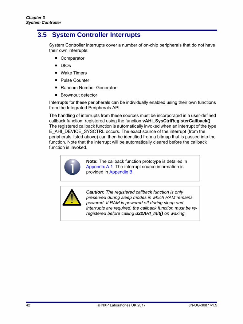
The above peripherals are illustrated in Figure 1.
For hardware details of these peripherals, refer to the relevant chip data sheet - see “Related Documents” on page 18.
JN-UG-3087 v1.5 © NXP Laboratories UK 2017 21

Chapter 1Overview
1.2 JN516x Integrated Peripherals API
The JN516x Integrated Peripherals API is a collection of C functions that can be incorporated in application code that runs on a JN516x wireless microcontroller in order to control the on-chip peripherals listed in Section 1.1. This API (sometimes referred to as the AHI) is defined in the header file AppHardwareApi.h, which is included in the NXP Software Developer’s Kits (SDKs) for the JN516x devices. The software that is invoked by this API is located in the on-chip ROM.
This API provides a thin software layer above the on-chip registers used to control the integrated peripherals. By encapsulating several register accesses into one function call, the API simplifies use of the peripherals without the need for a detailed knowledge of their operation.
Figure 1: JN516x Block Diagram
Caution: The JN516x Integrated Peripherals API functions are not re-entrant. A function must be allowed to complete before the function is called again, otherwise unexpected results may occur.
32-bit
RISC CPU4xPWM + Timer
2xUART
10-bit ADC
Battery and
Temp Sensors
2-Wire Serial (Master/Slave)
SPIMaster & SlaveRAM
128-bit AES
Hardware
2.4GHz
Including Diversity
Flash
Power
Management
XTAL
O-QPSK
Modem
EEPROM 20 DIO
Sleep Counter
Watchdog
Timer
Watchdog
Timer
Voltage Brownout
Radio
4-Channel
IEEE 802.15.4
Baseband
Processor
Encryption
22 © NXP Laboratories UK 2017 JN-UG-3087 v1.5

JN516x Integrated Peripherals APIUser Guide
Note that the Integrated Peripherals API does NOT include functions to control the:
IEEE 802.15.4 Baseband Processor built into the JN516x device - this is controlled by the wireless network protocol stack software (which may be an IEEE 802.15.4, ZigBee, JenNet or JenNet-IP stack), and APIs for this purpose are provided with the appropriate stack software product.
128-bit AES Hardware Encryption core built into the JN516x device - this is controlled using the functions described in the AES Coprocessor API Reference Manual (JN-RM-2013)
EEPROM - this is controlled using the Persistent Data Manager resident in the Jennic Operating System (JenOS). For further details, please refer to the JenOS User Guide (JN-UG-3075)
resources of the JN516x evaluation kit boards, such as sensors and display panels (although the buttons and LEDs on the evaluation kit boards are connected to the DIO pins of the JN516x device) - a special function library, called the LPRF Board API, is provided by NXP for this purpose and is described in the LPRF Board API Reference Manual (JN-RM-2003).
1.3 Using this Manual
The remainder of this manual is largely organised as one chapter per peripheral block. You should use the manual as follows:
1. First study Chapter 2 which describes the general functions that are not associated with one particular peripheral block. This chapter explains how to initialise the Integrated Peripherals API for use in your application code.
2. Next study Chapter 3 which describes the range of features associated with the System Controller. You may need to use one or more of these features in your application.
3. Then study those chapters in Part I: Concept and Operational Information which correspond to the particular peripherals that you wish to use in your application.
For full details of the referenced API functions, refer to Part II: Reference Information. Also note that interrupt handling is described in Part III: Appendices.
JN-UG-3087 v1.5 © NXP Laboratories UK 2017 23

Chapter 1Overview
24 © NXP Laboratories UK 2017 JN-UG-3087 v1.5

JN516x Integrated Peripherals APIUser Guide
2. General Functionality
This chapter describes use of the ‘general functions’ that are not associated with any of the peripheral blocks but may be needed in your application code (the API initialisation function will definitely be needed).
These functions cover the following areas:
API initialisation (Section 2.1)
Configuration of the radio transmission power (Section 2.2)
Use of the random number generator (Section 2.4)
Accessing the JN516x internal Non-Volatile Memory (Section 2.5)
Preserving debug information during sleep (Section 2.6)
2.1 API Initialisation
Before calling any other function from the JN516x Integrated Peripherals API, the function u32AHI_Init() must be called to initialise the API. This function must be called after every reset and wake-up (from sleep) of the JN516x microcontroller.
Caution: If you are using JenOS (Jennic Operating System), you must not call u32AHI_Init() explicitly in your code, as this function is called internally by JenOS. This applies principally to users who are developing ZigBee PRO applications.
JN-UG-3087 v1.5 © NXP Laboratories UK 2017 25

Chapter 2General Functionality
2.2 Radio Power
2.2.1 Transmission Power
The radio transmission power of a JN516x device can be varied. To set the transmission power, you can use the function eAppApiPlmeSet() from the NXP 802.15.4 Stack API (supplied in AppApi.h in all the JN516x SDKs). The required function call is:
eAppApiPlmeSet(PHY_PIB_ATTR_TX_POWER, x);
where x is a 6-bit two’s complement power level, corresponding to an input range of -32 to 31 dBm. In practice, this value is mapped to an actual transmission level:
For JN5168, JN5164 and JN5161, it is mapped to one of four levels: -32, -20, -9 and 0 dBm
For JN5169, it is mapped to the nearest of 26 levels in the range -32 to 10 dBm
Therefore, some positive input values will be truncated (to 10 dBm for the JN5169 device and to 0 dBm for the other JN516x devices).
2.2.2 Receive Power (JN5169 Only)
The JN5169 device can receive radio signals with power of up to 10 dBm before the input is saturated. However, it is possible to configure the device to saturate at a reduced incoming signal power of 0 dBm, which has the advantage of drawing less current and prolonging battery life. This reduced maximum input level can be enabled using the function vAHI_RadioSetReducedInputPower().
Note: The function bAHI_PhyRadioSetPower() has been removed from the JN516x Integrated Peripherals API. If updating existing code that previously used the function call bAHI_PhyRadioSetPower(y) then x in the above call to eAppApiPlmeSet() can be calculated as 34+10*y.
26 © NXP Laboratories UK 2017 JN-UG-3087 v1.5
JN516x Integrated Peripherals APIUser Guide
2.3 Antenna Diversity
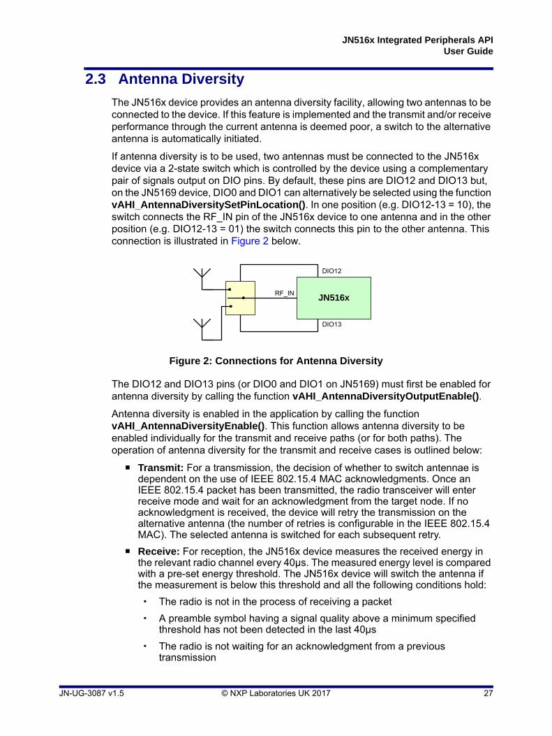
The JN516x device provides an antenna diversity facility, allowing two antennas to be connected to the device. If this feature is implemented and the transmit and/or receive performance through the current antenna is deemed poor, a switch to the alternative antenna is automatically initiated.
If antenna diversity is to be used, two antennas must be connected to the JN516x device via a 2-state switch which is controlled by the device using a complementary pair of signals output on DIO pins. By default, these pins are DIO12 and DIO13 but, on the JN5169 device, DIO0 and DIO1 can alternatively be selected using the function vAHI_AntennaDiversitySetPinLocation(). In one position (e.g. DIO12-13 = 10), the switch connects the RF_IN pin of the JN516x device to one antenna and in the other position (e.g. DIO12-13 = 01) the switch connects this pin to the other antenna. This connection is illustrated in Figure 2 below.
The DIO12 and DIO13 pins (or DIO0 and DIO1 on JN5169) must first be enabled for antenna diversity by calling the function vAHI_AntennaDiversityOutputEnable().
Antenna diversity is enabled in the application by calling the function vAHI_AntennaDiversityEnable(). This function allows antenna diversity to be enabled individually for the transmit and receive paths (or for both paths). The operation of antenna diversity for the transmit and receive cases is outlined below:
Transmit: For a transmission, the decision of whether to switch antennae is dependent on the use of IEEE 802.15.4 MAC acknowledgments. Once an IEEE 802.15.4 packet has been transmitted, the radio transceiver will enter receive mode and wait for an acknowledgment from the target node. If no acknowledgment is received, the device will retry the transmission on the alternative antenna (the number of retries is configurable in the IEEE 802.15.4 MAC). The selected antenna is switched for each subsequent retry.
Receive: For reception, the JN516x device measures the received energy in the relevant radio channel every 40µs. The measured energy level is compared with a pre-set energy threshold. The JN516x device will switch the antenna if the measurement is below this threshold and all the following conditions hold:
The radio is not in the process of receiving a packet
A preamble symbol having a signal quality above a minimum specified threshold has not been detected in the last 40µs
The radio is not waiting for an acknowledgment from a previous transmission
Figure 2: Connections for Antenna Diversity
JN516x RF_IN
DIO12
DIO13
JN-UG-3087 v1.5 © NXP Laboratories UK 2017 27

Chapter 2General Functionality
The signal energy and signal quality thresholds can be set by the application using the function vAHI_AntennaDiversityControl().
The current antenna diversity status can be obtained using the function u8AHI_AntennaDiversityStatus(). This function returns the antenna used for the last packet transmitted, the antenna used for the last packet received and the antenna that is currently selected.
The currently selected antenna can be manually switched by calling the function vAHI_AntennaDiversitySwitch(). Calling this function will generally not be required because it is expected that most applications will make use of the automatic transmit and/or receive antenna diversity control features that are enabled by calling vAHI_AntennaDiversityEnable().
2.4 Random Number Generator
The JN516x devices feature a random number generator which can produce 16-bit random numbers in one of two modes:
Single-shot mode: The generator produces one random number and stops.
Continuous mode: The generator runs continuously and generates a new random number every 256µs.
The random number generator can be started in either of the above modes using the function vAHI_StartRandomNumberGenerator(). This function also allows an interrupt to be enabled which is produced when a random number becomes available - this is handled as a System Controller interrupt by the callback function registered using the function vAHI_SysCtrlRegisterCallback() (see Section 3.5).
A randomly generated value can subsequently be read using the function u16AHI_ReadRandomNumber(). The availability of a new random number, and therefore the need to call the ‘read’ function, can be determined using either of the following methods:
Waiting for a random number generator interrupt, if enabled (see above)
Periodically calling the function bAHI_RndNumPoll() to poll for the availability of a new random value
When running in Continuous mode, the random number generator can be stopped using the function vAHI_StopRandomNumberGenerator().
Note: The random number generator uses the 32kHz clock domain (see Section 3.1) and will not operate properly if a high-precision external 32kHz clock source is used. Therefore, if generating random numbers in your application, you are advised to use the internal RC oscillator or a low-precision external clock source. You may also generate random numbers in your application before switching to a high-precision external clock.
28 © NXP Laboratories UK 2017 JN-UG-3087 v1.5

JN516x Integrated Peripherals APIUser Guide
2.5 Accessing Internal NVM
The JN516x device contains a small block of Non-Volatile Memory (NVM) which is organised as four 32-bit words numbered 0, 1, 2 and 3. This memory can be used to preserve important data (e.g. counter values) at times when the JN516x RAM is not powered - for example, during periods of sleep without RAM held.
Two functions are provided to access this memory:
vAHI_WriteNVData() can be used to write a 32-bit word of data to one of the four memory locations
u32AHI_ReadNVData() can be used to read a 32-bit word of data from one of the four memory locations
2.6 Preserving Debug Information Through Sleep
There are several registers within the JN516x CPU that are used during debug. The contents of these registers are not preserved during sleep (with or without RAM held), although they are preserved during Doze mode.
During sleep with memory held, the contents of these registers can be stored in RAM so that debug information is not lost - for example, to allow configured breakpoints to continue to work after sleep. Before the JN516x device is put to sleep (by calling vAHI_Sleep()), the contents of the registers should be saved to an array in RAM using the function vAHI_StoreDebug(). On waking from sleep, this data should then be restored from RAM to the Debug registers by calling the function vAHI_RestoreDebug() within AppWarmStart.
Caution: The contents of this JN516x NVM are not maintained when the microcontroller is completely powered off. However, they are maintained through a device reset.
JN-UG-3087 v1.5 © NXP Laboratories UK 2017 29

Chapter 2General Functionality
30 © NXP Laboratories UK 2017 JN-UG-3087 v1.5

JN516x Integrated Peripherals APIUser Guide
3. System Controller
This chapter describes use of the functions that control features of the System Controller.
These functions cover the following areas:
Clock management (Section 3.1)
Power management (Section 3.2)
Supply voltage monitoring (Section 3.3)
Chip reset (Section 3.4)
Interrupts (Section 3.5)
3.1 Clock Management
The System Controller provides clocks to the JN516x microcontroller and is divided into four main blocks - a system clock domain, a peripheral clock domain, a CPU clock domain and a 32kHz clock domain.
System Clock Domain
The system clock is a high-speed reference clock from which the peripheral clock and CPU clock are derived when the chip is fully operational. The clock for this domain is sourced from one of the following:
External 32MHz crystal oscillator
Internal high-speed RC oscillator
The crystal oscillator is driven from a 32MHz external crystal connected to device pins 4 and 5. The domain will produce a 32MHz system clock when sourced from the crystal oscillator.
The uncalibrated RC oscillator runs at 27MHz nominally, but can be calibrated to run at approximately 32MHz. The RC oscillator is mainly provided for a quick start-up following sleep, since the RC oscillator can start much more quickly than the crystal oscillator.
The radio transceiver and some peripherals should not be used when sourcing the system clock from the RC oscillator. System clock start-up and source selection is described in described in Section 3.1.1 and Section 3.1.2.
Peripheral Clock Domain
The peripheral clock is derived from the system clock and is used as the clock reference for the on-chip peripherals including the modem and baseband processor. The peripheral clock operates at half the system clock frequency - the peripheral clock runs at 16MHz when the system clock is sourced from the external 32MHz crystal oscillator.
JN-UG-3087 v1.5 © NXP Laboratories UK 2017 31

Chapter 3System Controller
CPU Clock Domain
The CPU clock is a divided down version of the system clock and is used as the clock reference for the microprocessor and memory subsystem. The CPU clock frequency selection is described in Section 3.1.3.
32kHz Clock Domain
The 32kHz clock domain is mainly used during low-power sleep states (but also for the random number generator on the JN516x device - see Section 2.4). While in Sleep mode (see Section 3.2.3), the CPU does not run and relies on an interrupt to wake it. The interrupt can be generated by an on-chip wake timer (see Chapter 8) or alternatively from an external source via a DIO pin (see Chapter 5), an on-chip comparator (see Section 4.3) or an on-chip pulse counter (see Chapter 11). The wake timers are driven from the 32kHz domain. The 32kHz clock for this domain can be sourced from one of the following:
Internal RC oscillator
External crystal
External clock module
The crystal oscillator is driven from an external 32kHz crystal connected to DIO9 and DIO10. If used, the external clock module is connected to DIO9.
Source clock selection for this domain is described in Section 3.1.5.
The 32kHz domain is still active when the chip is operating normally and can be calibrated against the peripheral clock to improve timing accuracy - see Section 8.2.
3.1.1 System Clock Start-up and Source Selection
As stated in the introduction to Section 3.1, there are two possible sources for the system clock on the JN516x device:
Internal high-speed RC oscillator
External crystal oscillator
where the crystal oscillator provides a more accurate clock than the RC oscillator.
Following a reset, the JN516x device takes its system clock from the internal high-speed RC oscillator. By default, an automatic switch to the external 32MHz crystal oscillator is performed once the crystal oscillator has stabilised (this can take up to 1ms). Application code is executed immediately following a reset.
Once the device and system clock are fully up and running, the system clock source can be changed using the function vAHI_SelectClockSource(). The identity of the current source clock can be obtained by calling the function bAHI_GetClkSource().
32 © NXP Laboratories UK 2017 JN-UG-3087 v1.5

JN516x Integrated Peripherals APIUser Guide
The RC Oscillator may be calibrated to improve its frequency accuracy by calling the function bAHI_TrimHighSpeedRCOsc().
It is important to note the following limitations while using the RC oscillator:
Uncalibrated, the RC oscillator will produce a system clock frequency of 27MHz ±18% (or 32MHz ±5% if calibrated)
The full system cannot be run while using the RC oscillator - it is possible to execute code but it is not possible to successfuly transmit or receive radio signals. Also, the peripheral clock may not be sufficiently accurate to support certain peripheral functions, such as UART communication.
Therefore, while using the RC oscillator, use of the radio transceiver should not be attempted, and the JN516x peripherals should be used with special care.
3.1.2 System Clock Start-up Following Sleep
By default, following sleep, the JN516x device takes its system clock from the internal high-speed RC oscillator, but performs an automatic switch to the external 32MHz crystal oscillator once the crystal oscillator has stabilised (can take up to 1ms). Thus, application code is executed immediately following sleep.
It is possible to continue using the internal high-speed RC oscillator (without the automatic switch). In this case, before going to sleep, it is necessary to call the function vAHI_EnableFastStartUp() with the manual switch option selected - this cancels the automatic switch to the crystal oscillator.
Note: If the external crystal oscillator is to be used as the source for the system clock, once the automatic switch to the crystal oscillator has occurred (bAHI_GetClkSource() == FALSE), the function vAHI_OptimiseWaitStates() should be called. This function optimises the wait states for the JN516x internal Flash memory and EEPROM according to the system clock frequency in order to minimise access times.
JN-UG-3087 v1.5 © NXP Laboratories UK 2017 33

Chapter 3System Controller
3.1.3 CPU Clock Frequency Selection
A range of CPU clock frequencies are available on the JN516x device. By default, the source clock frequency is halved to produce the CPU clock. Thus:
Using the external crystal oscillator, the 32MHz source frequency will produce a CPU clock frequency of 16MHz
Using the uncalibrated internal high-speed RC oscillator, the 27MHz source frequency will produce a CPU clock frequency of 13.5MHz (±18%).
However, alternative CPU clock frequencies can be configured using the function bAHI_SetClockRate(). A division factor must be specified for dividing down the source clock to produce the CPU clock. The possible division factors are 1, 2, 4, 8, 16 and 32:
For a source clock of 32MHz, the possible CPU clock frequencies are then 1, 2, 4, 8, 16 and 32 MHz
For a source clock of 27MHz, the possible CPU clock frequencies are then 0.84, 1.17, 3.38, 6.75, 13.5 and 27 MHz.
3.1.4 System Clock Operation at High Temperatures
When the external crystal oscillator is operating at high temperatures, typically in excess of 85°C depending on the oscillator’s characteristics, it will run fast. In this case, it may be necessary to call the function vAHI_ClockXtalPull() to decrease (pull) the frequency and maintain the frequency tolerance within the 40ppm limit specified by the IEEE 802.15.4 standard. This frequency pulling is achieved by increasing the crystal load capacitance in the oscillator tuning circuit. The required additional capacitance must be specified in the function call and the available values are different between the JN5169 and other JN516x devices. For a detailed description of frequency pulling, refer to the description of vAHI_ClockXtalPull() on page 173.
Note: The frequency of the high-speed RC oscillator can be adjusted to a calibrated 32MHz by calling bAHI_TrimHighSpeedRCOsc().
34 © NXP Laboratories UK 2017 JN-UG-3087 v1.5

JN516x Integrated Peripherals APIUser Guide
3.1.5 32kHz Clock Selection
As stated in the introduction to Section 3.1, a choice of source for the 32kHz clock is available on the JN516x device. The selection of this source clock is detailed below.
The 32kHz clock can be optionally sourced from an external crystal or clock module. One of these external clock sources can be selected using the function bAHI_Set32KhzClockMode(). If required, this function should be called near the start of the application.
If selecting the external crystal oscillator using bAHI_Set32KhzClockMode(), this function must be called before Timer 0 and any Wake Timers are used by the application, since these timers are used by the function when switching the clock source to the external crystal. This function starts the external crystal, which can take up to 1 second to stabilise, and the function waits for the crystal to become ready before returning.
Alternatively, if the external crystal oscillator is required, the function vAHI_Init32KhzXtal() can be called to start the crystal and switch to it immediately. This function returns straight away but the clock will take up to 1 second to stabilise. While waiting for the crystal to become stable, the application can perform other processing or put the JN516x device into sleep mode - in the case of sleep, the application should typically set a wake timer to wake the device after 1 second.
If selecting the external clock module (RC circuit), the accuracy of the clock frequency produced can be chosen by setting the current consumption of the circuit using the function vAHI_Trim32KhzRC().
The connections to the external clock source must be made as follows:
The external clock module must be supplied on DIO9. You must first disable the pull-up on DIO9 using the function vAHI_DioSetPullup().
The external crystal oscillator must be attached on DIO9 and DIO10. The pull-ups on DIO9 and DIO10 are disabled automatically.
Note that there is no need to explicitly configure DIO9 or DIO10 as an input, as this is done automatically by bAHI_Set32KhzClockMode() and by vAHI_Init32KhzXtal().
Note: The default clock source is the internal 32kHz RC oscillator. The functions described below only need to be called if an external 32kHz clock source is required. Once an external source has been selected, it is not possible to switch back to the internal RC oscillator.
JN-UG-3087 v1.5 © NXP Laboratories UK 2017 35

Chapter 3System Controller
3.2 Power Management
This section describes how to control the power to a JN516x microcontroller using the Integrated Peripherals API. This includes control of the power regulator that supplies certain on-chip peripherals and the management of low-power sleep modes.
3.2.1 Power Domains
A JN516x microcontroller has a number of power domains, as follows:
Digital Logic domain: This domain supplies the CPU and digital peripherals as well as the wireless transceiver (including encryption coprocessor and baseband controller). The clock from this domain to the wireless transceiver can be enabled/disabled by the application (see Section 3.2.2). The domain is always unpowered during sleep.
Analogue domain: This domain supplies the ADC. The domain is switched on when the function vAHI_ApConfigure() is called to configure the analogue peripherals - see Chapter 4. The domain is always unpowered during sleep.
RAM domain: This domain supplies the on-chip RAM. The domain may be powered or unpowered during sleep.
Radio domain: This domain supplies the radio transceiver. The domain is always unpowered during sleep.
VDD Supply domain: This domain supplies the wake timers, DIO blocks, comparator and 32kHz oscillators. The domain is driven from the external supply (battery) and is always powered. However, the wake timers and 32kHz oscillators may be powered or unpowered during sleep.
Separate voltage regulators for the CPU (Digital Logic domain) and on-chip RAM provide flexibility in implementing different low-power sleep modes, allowing the memory to be either powered (and its contents maintained) or unpowered while the CPU is powered down - for further information on sleep modes, refer to Section 3.2.3.
36 © NXP Laboratories UK 2017 JN-UG-3087 v1.5

JN516x Integrated Peripherals APIUser Guide
3.2.2 Wireless Transceiver Clock
The clock to the wireless transceiver can be enabled/disabled using the function vAHI_ProtocolPower(). However, disabling this clock outside of a reset or sleep cycle must be done with caution. The following points should be noted:
Disabling this clock leaves the clock powered but disabled (gated).
Disabling the clock causes the IEEE 802.15.4 MAC settings to be lost. Therefore, you must save the current MAC settings before disabling the clock. On re-enabling the clock, the MAC settings must be restored from the saved settings. You can save and restore the MAC settings using functions of the 802.15.4 Stack API, described in the IEEE 802.15.4 Stack User Guide (JN-UG-3024):
To save the MAC settings, use the function vAppApiSaveMacSettings().
To restore the saved MAC settings, use the function vAppApiRestoreMacSettings() - the clock is automatically re-enabled, since this function calls vAHI_ProtocolPower().
Do not call vAHI_ProtocolPower() to disable the clock while the 802.15.4 MAC layer is active, otherwise the microcontroller may freeze.
While the clock is disabled, do not make any calls into the stack, as this may result in the stack attempting to access the associated hardware (which is disabled) and therefore cause an exception.
JN-UG-3087 v1.5 © NXP Laboratories UK 2017 37

Chapter 3System Controller
3.2.3 Low-Power Modes
The JN516x microcontroller is able to enter a number of low-power modes in order to conserve power during periods when the device does not need to be fully active. Generally, there are two low-power modes, Sleep mode (including Deep Sleep) and Doze mode, described below.
Sleep and Deep Sleep Modes
In Sleep mode, most of the internal chip functions are shut down to save power, including the CPU and the majority of on-chip peripherals. However, the states of the DIO pins are retained, including the output values and pull-up enables, which preserves any interface to the outside world. The on-chip RAM, the 32kHz oscillator, the comparator and the pulse counter can optionally remain active during sleep.
Sleep mode is started using the function vAHI_Sleep(), when one of four sleep modes can be selected which depend on whether RAM and the 32kHz oscillator are to be powered off. The significance of the 32kHz oscillator and RAM during sleep is outlined below:
32kHz Oscillator: The 32kHz oscillator (internal RC, external clock or external crystal) can, in theory, be either left running or stopped for the duration of sleep. However, this oscillator is used by the wake timers and must be left running if a wake timer will be used to wake the device from sleep. Also, if an external source is used for this oscillator, it is not recommended that the oscillator is stopped on entering sleep mode.
On-chip RAM: Power to on-chip RAM can be either maintained or removed during sleep. The application program, stack context data and application data are all held in on-chip RAM while the microcontroller is fully active, but are lost if the power to RAM is switched off.
If the power to RAM is removed during sleep, the application is re-loaded into RAM from on-chip Flash memory on exiting sleep mode. Stack context and application data may also be re-loaded by the application, if they were saved to the on-chip EEPROM before entering sleep mode.
If the power to RAM is maintained during sleep, the application and data will be preserved. This option is useful for short sleep periods, when the time taken on waking to re-load the application and data into RAM is significant compared with the sleep duration.
A further low-power option is Deep Sleep mode in which the CPU, RAM and both the system and 32kHz clock domains are powered down. In addition, any external Flash memory is also powered down during Deep Sleep mode. This option obviously provides a bigger power saving than Sleep mode.
Note: If the pulse counter is to be run with debounce while the device is asleep, the 32kHz oscillator must be left running - see Chapter 11.
38 © NXP Laboratories UK 2017 JN-UG-3087 v1.5

JN516x Integrated Peripherals APIUser Guide
The microcontroller can be woken from Sleep mode by one of the following:
DIO interrupt (see Chapter 5)
Wake timer interrupt (needs 32kHz oscillator to be running - see Chapter 8)
Comparator interrupt (see Section 4.3)
Pulse counter interrupt (see Chapter 11)
The device can only be woken from Deep Sleep mode by its reset line being pulled low or by an external event which triggers a change on a DIO pin.
When the device restarts, it will begin processing at the cold start or warm start entry point, depending on the sleep mode from which the device is waking.
Doze Mode
Doze mode is a low-power mode in which the CPU, RAM, radio transceiver and digital peripherals remain powered but the clock to the CPU is stopped (all other clocks continue as normal). This mode provides less of a power saving than Sleep mode but allows a quicker recovery back to full working mode. Doze mode is useful for very short periods of low power consumption - for example, while waiting for a timer event or for a transmission to complete.
The CPU can be put into Doze mode by calling the function vAHI_CpuDoze(). It is subsequently brought out of Doze mode by any interrupt.
3.2.4 Power Status
The power status of the JN516x microcontroller can be obtained using the function u16AHI_PowerStatus(). This function returns a bitmap which indicates whether:
The device has completed a sleep-wake cycle
RAM contents were retained during sleep
The analogue power domain is switched on
The protocol logic is operational - clock is enabled
Watchdog timeout was responsible for the last device restart
32kHz clock is ready (e.g. following a reset or wake-up)
Device has just come out of Deep Sleep mode (rather than a reset)
For further details of the bitmap, refer to the function descriptions in Chapter 19.
Note: External NVM is not powered down during normal Sleep mode. If required, you can power down an external Flash memory device using the function vAHI_FlashPowerDown(), which must be called before vAHI_Sleep(), provided you are using a compatible Flash device. For full details, refer to Section 16.4.
JN-UG-3087 v1.5 © NXP Laboratories UK 2017 39

Chapter 3System Controller
3.3 Supply Voltage Monitor (SVM)
A ‘brownout’ is a fall in the supply voltage to a device or system below a pre-defined level, which may hinder or be harmful to the operation of the device/system. The JN516x microcontroller is equipped with a Supply Voltage Monitor (SVM) to detect the brownout condition. SVM can be configured and monitored through functions of the Integrated Peripherals API.
3.3.1 Configuring SVM
By default on the JN516x device, the SVM feature is automatically enabled and the brownout voltage is set to 2.0V. On detection of a brownout, the chip will be automatically reset.
The SVM settings can be changed from the default values by calling the function vAHI_BrownOutConfigure(), which allows the configuration of the following:
SVM enable/disable: The SVM feature can be enabled/disabled - if the configuration function is called and SVM is required, the feature must be explicitly enabled in the function.
Brownout level: The brownout voltage level can be set to one of the following values: 1.95V, 2.0V (default), 2.1V, 2.2V, 2.3V, 2.4V, 2.7V or 3.0V
Reset on brownout: The automatic reset on the occurrence of a brownout can be enabled/disabled.
Brownout interrupts: Two separate interrupts relating to brownout can be enabled/disabled:
An interrupt can be generated when the device enters the brownout state (supply voltage falls below the brownout voltage level).
An interrupt can be generated when the device leaves the brownout state (supply voltage rises above the brownout voltage level).
After the return of the configuration function, there will be a delay before the new settings take effect - this delay is up to 3.3µs.
Note: Following a device reset or sleep, the default SVM settings are re-instated.
40 © NXP Laboratories UK 2017 JN-UG-3087 v1.5

JN516x Integrated Peripherals APIUser Guide
3.3.2 Monitoring Voltage
Provided that SVM is enabled (see Section 3.3.1), the brownout status of the JN516x device can be monitored in one of three ways: automatic reset, interrupts or polling. These options are described below.
Automatic Reset on Brownout
An automatic reset on a brownout is enabled by default, but can also be enabled/disabled through the function vAHI_BrownOutConfigure(). Following a chip reset, the application can check whether a brownout was the cause of the reset by calling the function bAHI_BrownOutEventResetStatus().
Brownout Interrupts
Interrupts can be generated when the device enters the brownout state and/or when it exits the brownout state. These two interrupts can be individually enabled/disabled through the function vAHI_BrownOutConfigure(). Brownout interrupts are System Controller interrupts and are handled by the callback function registered using the function vAHI_SysCtrlRegisterCallback() - see Section 3.5.
Polling for Brownout
If brownout interrupts and automatic reset are disabled (but SVM is still enabled), the brownout state of the device can be obtained by manually polling via the function u32AHI_BrownOutPoll(). This function will indicate whether the supply voltage is currently above or below the brownout level.
3.4 Resets
The JN516x microcontroller can be reset from the application using the function vAHI_SwReset(). This function initiates the full reset sequence for the chip and is the equivalent of pulling the external RESETN line low. Note that during a chip reset, the contents of on-chip RAM are likely to be lost.
One or more external devices may also be connected to the RESETN line. Thus, any external devices connected to this line may be affected.
Note: An external RC circuit can be connected to the RESETN line in order to generate a reset. The required resistance and capacitance values are specified in the data sheet for the microcontroller.
JN-UG-3087 v1.5 © NXP Laboratories UK 2017 41
Chapter 3System Controller
3.5 System Controller Interrupts
System Controller interrupts cover a number of on-chip peripherals that do not have their own interrupts:
Comparator
DIOs
Wake Timers
Pulse Counter
Random Number Generator
Brownout detector
Interrupts for these peripherals can be individually enabled using their own functions from the Integrated Peripherals API.
The handling of interrupts from these sources must be incorporated in a user-defined callback function, registered using the function vAHI_SysCtrlRegisterCallback(). The registered callback function is automatically invoked when an interrupt of the type E_AHI_DEVICE_SYSCTRL occurs. The exact source of the interrupt (from the peripherals listed above) can then be identified from a bitmap that is passed into the function. Note that the interrupt will be automatically cleared before the callback function is invoked.
Note: The callback function prototype is detailed in Appendix A.1. The interrupt source information is provided in Appendix B.
Caution: The registered callback function is only preserved during sleep modes in which RAM remains powered. If RAM is powered off during sleep and interrupts are required, the callback function must be re-registered before calling u32AHI_Init() on waking.
42 © NXP Laboratories UK 2017 JN-UG-3087 v1.5
JN516x Integrated Peripherals APIUser Guide
4. Analogue Peripherals
This chapter describes control of the analogue peripherals using functions of the Integrated Peripherals API.
The are two types of analogue peripheral on the JN516x microcontroller:
Analogue-to-Digital Converter [ADC] (Section 4.1)
Comparator (Section 4.3)
Analogue peripheral interrupts are described in Section 4.4.
4.1 ADC
The JN516x microcontroller includes a 10-bit Analogue-to-Digital Converter (ADC). The ADC samples an analogue input signal to produce a digital representation of the input voltage. It samples the input voltage at one instant in time and holds this voltage (in a capacitor) while converting it to a 10-bit binary value - the total sample/convert duration is called the conversion time.
The ADC may sample periodically to produce a sequence of digital values representing the behaviour of the input voltage over time. The rate at which the sampling events take place is called the sampling frequency. According to the Nyquist sampling theorem, the sampling frequency must be at least twice the highest frequency to be measured in the input signal. If the input signal contains frequencies of more than half the sampling frequency, these frequencies will be aliased. To prevent aliasing, a low-pass filter should be applied to the ADC input in order to remove frequencies greater than half the sampling frequency.
The ADC can take its analogue input from an external source, an on-chip temperature sensor and an internal voltage monitor (see below). The input voltage range is also selectable as between zero and a reference voltage, or between zero and twice this reference voltage (see below).
When using the ADC, the first analogue peripheral function to be called must be vAHI_ApConfigure(), which allows the following properties to be configured:
Clock:
The clock input for the ADC is provided by the peripheral clock, normally 16MHz (see Section 3.1 for system clock options), which is divided down. The target frequency is selected using vAHI_ApConfigure(). The recommended target frequency for the ADC is 500kHz.
Note: When an ADC input which is shared with a DIO is used, the associated DIO should be configured as an input with the pull-up disabled (refer to Section 5.1.1 and Section 5.1.3).
JN-UG-3087 v1.5 © NXP Laboratories UK 2017 43

Chapter 4Analogue Peripherals
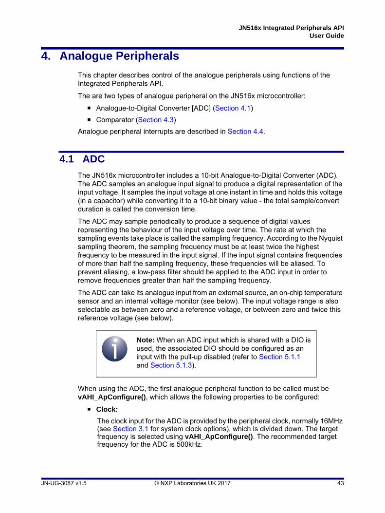
Sampling interval and conversion time:
The sampling interval determines the time over which the ADC will integrate the analogue input voltage before performing the conversion - in fact, the integration occurs over three times this interval (see Figure 3). This interval is set as a multiple of the ADC clock period (2x, 4x, 6x or 8x), where this multiple is selected using vAHI_ApConfigure(). Normally, it should be set to 2x - for details, refer to the data sheet for the microcontroller.
The time allowed to perform the subsequent conversion is 13 clock periods. Thus, the total time to sample and convert (the conversion time) is given by:
[(3 x sampling interval) + 13] x clock period
For a visual illustration, refer to Figure 3.
Reference voltage:
The permissible range for the analogue input voltage is defined relative to a reference voltage Vref, which can be sourced internally or externally. The source of Vref is selected using vAHI_ApConfigure().
The input voltage range can be selected as either 0 to Vref or 0 to 2Vref, which is selected the vAHI_AdcEnable() function - see later.
Voltage regulator:
In order to minimise the amount of digital noise in the ADC, the device is powered from a voltage regulator, sourced from the analogue supply VDD1. The regulator (and therefore power) can be enabled/disabled using vAHI_ApConfigure(). Once enabled, it is necessary to wait for the regulator to stabilise - the function bAHI_APRegulatorEnabled() can be used to check whether the regulator is ready.
Interrupt:
Interrupts can be enabled such that an interrupt (of the type E_AHI_DEVICE_ANALOGUE) is generated after each individual conversion. This is particularly useful for ADC continuous (periodic) conversion. Interrupts can be enabled/disabled using vAHI_ApConfigure(). Analogue peripheral interrupt handling is described in Section 4.4.
The ADC must then be further configured and enabled (but not started) using the function vAHI_AdcEnable(). This function allows the following properties to be configured.
Input source:
The ADC can take its input from one of a number of multiplexed sources comprising external pins (shared with DIOs), an on-chip temperature sensor and an internal voltage monitor. Six external input pins are available on the JN5169 device and four pins on all other JN516x devices. The input is selected using vAHI_AdcEnable().
Input voltage range:
The permissible range for the analogue input voltage is defined relative to the reference voltage Vref. The input voltage range can be selected as either 0 to Vref or 0 to 2Vref (an input voltage outside this range results in a saturated digital output). The analogue voltage range is selected using vAHI_AdcEnable().
44 © NXP Laboratories UK 2017 JN-UG-3087 v1.5
JN516x Integrated Peripherals APIUser Guide
Conversion mode:
The ADC can be configured to perform conversions in the following modes:
Single-shot: A single conversion is performed (see Section 4.1.1).
Continuous: Conversions are performed repeatedly (see Section 4.1.2).
Accumulation: A fixed number of conversions are performed and the results are added together (see Section 4.1.3).
Single-shot mode or continuous mode can be selected using vAHI_AdcEnable(). In all three cases, the conversion time for an individual conversion is given by [(3 x sampling interval) + 13] x clock period, which is illustrated in Figure 3. In the cases of continuous mode and accumulation mode, after this time the next conversion will start and the sampling frequency will be the reciprocal of the conversion time.
Once the ADC has been configured using first vAHI_ApConfigure() and then vAHI_AdcEnable(), conversion can be started in one of the available modes. Operation of the ADC in these modes is described in the subsections below:
Single-shot mode: Section 4.1.1
Continuous mode: Section 4.1.2
Accumulation mode: Section 4.1.3
Note that only the ADC can generate analogue peripheral interrupts (of the type E_AHI_DEVICE_ANALOGUE) - these interrupts are handled by a user-defined callback function registered via vAHI_APRegisterCallback(). Refer to Section 4.4 for more information on analogue peripheral interrupt handling.
Figure 3: ADC Sampling
3 x sampling interval *
* Sampling interval is defined as 2, 4, 6 or 8 clock cycles
13 xclock cycles
ADC uses this time to perform the conversion
ADC captures analogue input during this time
JN-UG-3087 v1.5 © NXP Laboratories UK 2017 45

Chapter 4Analogue Peripherals
4.1.1 Single-Shot Mode
In single-shot mode, the ADC performs one conversion and then stops. To operate in this way, single-shot mode must have been selected when the ADC was enabled using vAHI_AdcEnable(). The conversion can then be started using the function vAHI_AdcStartSample().
Completion of the conversion can be detected in one of two ways:
An interrupt can be generated on completion - in this case, analogue peripheral interrupts must have been enabled in the function vAHI_ApConfigure().
The function bAHI_AdcPoll() can be used to check whether the conversion has completed.
Once the conversion has been performed, the result can be obtained using the function u16AHI_AdcRead().
4.1.2 Continuous Mode
In continuous mode, the ADC performs repeated conversions indefinitely (until stopped). To operate in this way, continuous mode must have been selected when the ADC was enabled using vAHI_AdcEnable(). The conversions can then be started using the function vAHI_AdcStartSample().
The sampling frequency in continuous mode is given by the reciprocal of the conversion time, where:
Conversion time = [(3 x sampling interval) + 13] x clock period
Completion of an individual conversion can be detected in one of two ways:
An interrupt can be generated on completion - in this case, analogue peripheral interrupts must have been enabled in the function vAHI_ApConfigure().
The function bAHI_AdcPoll() can be used to check whether the conversion has completed.
Once an individual conversion has been performed, the result can be obtained using the function u16AHI_AdcRead(). The result remains available to be read by this function until the next conversion has completed.
The conversions can be stopped using the function vAHI_AdcDisable().
46 © NXP Laboratories UK 2017 JN-UG-3087 v1.5

JN516x Integrated Peripherals APIUser Guide
4.1.3 Accumulation Mode
In accumulation mode, the ADC performs a fixed number of conversions and then stops. The results of these conversions are added together to allow them to be averaged. To operate in this mode, the conversions must be started using the function vAHI_AdcStartAccumulateSamples(). The number of conversions is selected in this function as 2, 4, 8 or 16.
The sampling frequency in accumulation mode is given by the reciprocal of the conversion time, where:
Conversion time = [(3 x sampling interval) + 13] x clock period
Completion of ALL the conversions can be detected in one of two ways:
An interrupt can be generated on completion - in this case, analogue peripheral interrupts must have been enabled in the function vAHI_ApConfigure().
The function bAHI_AdcPoll() can be used to check whether the conversions have completed.
Once the conversions have been performed, the cumulative result can be obtained using the function u16AHI_AdcRead(). Note that this function delivers the sum of the results for individual conversions - the averaging calculation must be performed by the application (by dividing by the number of conversions).
The conversions can be stopped at any time using the function vAHI_AdcDisable().
Note: When the ADC is started in accumulation mode, the conversion mode selected in vAHI_AdcEnable() is ignored.
JN-UG-3087 v1.5 © NXP Laboratories UK 2017 47

Chapter 4Analogue Peripherals
4.2 ADC with DMA Engine (Sample Buffer Mode)
This section describes an operational mode of the ADC in which it is used in conjunction with the DMA (Direct Memory Access) engine on the JN516x device. In this mode:
ADC 10-bit data samples are produced at regular intervals and transferred into a buffer in RAM as 16-bit samples, where this data transfer and storage is performed by the DMA engine independently of the CPU
The CPU can perform other tasks while the data transfer and storage is being managed by the DMA engine - the CPU only needs to initiate the ADC conversions and deal with the results in the buffer (when an interrupt occurs)
ADC sampling can be multiplexed between different analogue sources
This method of using the ADC is called ‘sample buffer mode’.
The ADC samples are produced at a configurable rate and are timed using one of the on-chip timers (Timer 0, 1, 2, 3 or 4).
The application running on the CPU can service the buffer when the latter has collected sufficient data to cause an interrupt. The application must register a callback function to service this interrupt.
4.2.1 Preparing for Sample Buffer Mode
Before sample buffer mode can be enabled and started (see Section 4.2.2), the following preparations must be carried out:
The function vAHI_ApConfigure() must be called to perform the initial configuration of the ADC (including clock frequency for conversion, sampling interval for conversion, reference voltage for input, use of voltage regulator and use of interrupts), as described for other ADC modes in Section 4.2.
A JN516x timer to trigger the repeated conversions must be set up and started, as described in Chapter 7. Note the following:
This timer can be any one of Timers 0 to 4 (the required timer is specified later when sample buffer mode is enabled and started - see Section 4.2.2)
DIOs are not needed by this timer and may be released for other uses (see Section 7.2.1)
Timer interrupts are not required and should be disabled for this timer when vAHI_TimerEnable() is called (see Section 7.2.2)
The timer must be configured and started in ‘Timer repeat’ mode using vAHI_TimerStartRepeat() (see Section 7.3.1)
A user-defined callback function to handle the interrupts generated in sample buffer mode must be registered using vAHI_APRegisterCallback(), as described in Section 4.4 (the required interrupt mode is specified later when sample buffer mode is enabled and started - see Section 4.2.2).
48 © NXP Laboratories UK 2017 JN-UG-3087 v1.5

JN516x Integrated Peripherals APIUser Guide
4.2.2 Sample Buffer Mode Operation
Once sample buffer mode has been prepared as described in Section 4.2.1 (ADC configuration, timer started, callback function registered), operation in this mode can be further configured and started using bAHI_AdcEnableSampleBuffer(). The following configuration must be carried out in this function call:
The required JN516x timer must be specified as one of Timers 0 to 4
The input voltage range must be specified as either 0 to Vref or 0 to 2Vref, where the reference voltage Vref has been specified in vAHI_ApConfigure()
A bitmap must be provided which specifies the analogue input sources that will be multiplexed in this ADC mode - the possible sources include external input pins, an on-chip temperature sensor and an internal voltage monitor
The RAM buffer to receive the data must be fully specified, as follows:
A pointer to the start of the buffer
The size of the buffer (in 16-bit samples, up to a maximum of 2047)
Whether the buffer will wrap around to the start (when it becomes full)
The DMA interrupt mode to be used must be specified as one of:
Interrupt when the buffer fills to its mid-point
Interrupt when the buffer is full
Interrupt when the buffer has wrapped around to its start
If operation in this mode is continuous (the buffer wraps around), it can be stopped using the function vAHI_AdcDisableSampleBuffer().
Notes on various aspects of sample buffer mode operation (input multiplexing, buffer wrap and DMA interrupts) are provided below.
Input Multiplexing
Sample buffer mode allows a number of analogue inputs to be multiplexed. These inputs comprise external inputs ADC1-4 (and ADC5-6 on JN5169), an on-chip temperature sensor and an internal voltage monitor. The required multiplexed inputs are specified through a bitmap in the call to bAHI_AdcEnableSampleBuffer().
16-bit samples from all the selected inputs will be produced on each timer trigger. These samples will be produced (and stored in the buffer) in the following order:
1. External input ADC1
2. External input ADC2
3. External input ADC3
4. External input ADC4
5. External input ADC5 (JN5169 only)
6. External input ADC6 (JN5169 only)
7. Temperature sensor
8. Voltage monitor
JN-UG-3087 v1.5 © NXP Laboratories UK 2017 49

Chapter 4Analogue Peripherals
Buffer Wrap
In the call to bAHI_AdcEnableSampleBuffer(), the RAM buffer can be configured to wrap around:
If the buffer wrap option is enabled then when the buffer becomes full, data will continue to be written from the start of the buffer again. In this case, earlier data will be over-written and will be lost unless the buffer has been read by the application. The application can be alerted of a full buffer using the ‘buffer full’ interrupt (see DMA Interrupts below).
If the buffer wrap option is not enabled then when the buffer becomes full, an overflow condition will exist on the production of the next data sample. In this case, no new data can be stored until the buffer is read by the application. The application can be alerted of a full buffer using the ‘buffer full’ interrupt and of an overflow situation using the ‘buffer overflow’ interrupt (see DMA Interrupts below).
In both of the above cases, the application should ensure that data is promptly read from the buffer in order to avoid losing data.
DMA Interrupts
DMA interrupts are used to notify the application of the status of the RAM buffer. These interrupts are as follows:
Buffer half-full: The buffer has been half-filled with data
Buffer full: The buffer has been completely filled with data:
If the buffer wrap option is enabled then the buffer will wrap around
If the buffer wrap option is disabled then the buffer will overflow if not read
Buffer overflow: The buffer has been completely filled with data and a new data sample is available which cannot be stored and will be lost (applicable when the buffer wrap option has been disabled)
One or more of the above interrupt conditions can be selected in the call to bAHI_AdcEnableSampleBuffer(). These interrupts must be serviced by the user-defined callback function registered using vAHI_APRegisterCallback().
50 © NXP Laboratories UK 2017 JN-UG-3087 v1.5

JN516x Integrated Peripherals APIUser Guide
4.3 Comparator
The JN516x microcontroller includes one comparator (numbered 1).
The comparator can be used to compare two analogue inputs. It changes its two-state digital output (high to low or low to high) when the arithmetic difference between the inputs changes sense (positive to negative or negative to positive). The comparator can be used as a basis for measuring the frequency of a time-varying analogue input when compared with a constant reference input.
One analogue input carries the externally sourced signal to be monitored - the input voltage must always remain within the range 0V to Vdd (the chip supply voltage). This external signal can be supplied on the comparator’s ‘positive’ pin (COMP1P) or ‘negative’ pin (COMP1M). It will be compared with a reference signal, which can be sourced internally or externally as follows:
externally from the other comparator pin (COMP1P or COMP1M) that is not being used for the monitored input signal
internally from the reference voltage Vref (the source of Vref is selected using the function vAHI_ApConfigure())
The input and reference signals are selected from the above options via the function vAHI_ComparatorEnable(), which is used to configure and enable the comparator.
The comparator has two possible states - high or low. The comparator state is determined by the relative values of the two analogue input voltages - that is, by the instantaneous voltages of the signal under analysis, Vsig, and the reference signal, Vrefsig. The relationships are as follows:
Vsig > Vrefsig high
Vsig < Vrefsig low
or in terms of differences:
Vsig - Vrefsig > 0 high
Vsig - Vrefsig < 0 low
Thus, as the signal levels vary with time, when Vsig rises above Vrefsig or falls below Vrefsig, the state of the comparator result changes. In this way, Vrefsig is used as the threshold against which Vsig is assessed.
Note 1: By default, the comparator is enabled in low-power mode. Refer to Section 4.3.2 for more details.
Note 2: Calling vAHI_ComparatorEnable() while the ADC is operating may lead to corruption of the ADC results. Therefore, if required, this function should be called before starting the ADC.
Note 3: When a comparator pin is used, the associated DIO should be configured as an input with the pull-up disabled (refer to Section 5.1.1 and Section 5.1.3).
JN-UG-3087 v1.5 © NXP Laboratories UK 2017 51

Chapter 4Analogue Peripherals
In reality, this method of functioning is sensitive to noise in the analogue input signals causing spurious changes in the comparator state. This situation can be improved by using two different thresholds:
An upper threshold, Vupper, for low-to-high transitions
A lower threshold, Vlower, for high-to-low transitions
The thresholds Vupper and Vlower are defined such that they are above and below the reference signal voltage Vrefsig by the same amount, where this amount is called the hysteresis voltage, Vhyst.
That is:
Vupper = Vrefsig + Vhyst
Vlower = Vrefsig - Vhyst
The hysteresis voltage is selected using the vAHI_ComparatorEnable() function. It can be set to 0, 5, 10 or 20 mV. The selected hysteresis level should be larger than the noise level in the input signal.
The comparator two-threshold mechanism is illustrated in Figure 4 below for the case when the reference signal voltage Vrefsig is constant.
Note that there is a time delay between a change in the comparator inputs and the resulting state reported by the comparator.
As well as configuring the comparator, vAHI_ComparatorEnable() also starts operation of the comparator. The current state of the comparator (high or low) can be obtained at any time using the function u8AHI_ComparatorStatus(). The comparator can be stopped at any time using the function vAHI_ComparatorDisable().
Figure 4: Upper and Lower Thresholds of Comparator
Vsig
t
Vupper
Vlower
Vrefsig2Vhyst
Comparator state:
Low to High
Comparator state:
High to Low
52 © NXP Laboratories UK 2017 JN-UG-3087 v1.5

JN516x Integrated Peripherals APIUser Guide
4.3.1 Comparator Interrupts and Wake-up
The comparator allows an interrupt to be generated on either a low-to-high or high-to-low transition. Interrupts can only be produced on transitions in one direction (and not both). Interrupts can be enabled using the function vAHI_ComparatorIntEnable(). The function is used to both enable/disable comparator interrupts and select the direction of the transitions that will trigger the interrupts.
A comparator interrupt can be used as a signal to wake a node from sleep - this is then referred to as a ‘wake-up interrupt’. To use this feature, interrupts must be configured and enabled using vAHI_ComparatorIntEnable(), as described above. Note that during sleep, the reference signal Vrefsig is taken from an external source via the ‘negative’ pin COMP1M or the ‘positive’ pin COMP1P, whichever is used during wake periods. The wake-up interrupt status can be checked using the function u8AHI_ComparatorWakeStatus().
4.3.2 Comparator Low-Power Mode
The comparator is able to operate in a low-power mode, in which it draws only 0.8µA of current, compared with 73µA when operating in standard-power mode. Comparator low-power mode can be enabled/disabled using the function vAHI_ComparatorLowPowerMode().
When a comparator is configured and started using vAHI_ComparatorEnable(), it operates in standard-power mode. To operate the comparator in low-power mode, the function vAHI_ComparatorLowPowerMode() must then be called.
Low-power mode is beneficial in helping to minimise the current drawn by a device that employs energy harvesting. It is also automatically enabled during sleep in order to optimise the energy conserved. The disadvantage of low-power mode is a slower response time for the comparator - that is, a longer delay between a change in the comparator inputs and the resulting state reported by the comparator. However, if the response time is not important, low-power mode should normally be used.
Important: Comparator interrupts are System Controller interrupts and not analogue peripheral interrupts. They must therefore be handled by a callback function that is registered via vAHI_SysCtrlRegisterCallback().
JN-UG-3087 v1.5 © NXP Laboratories UK 2017 53
Chapter 4Analogue Peripherals
4.4 Analogue Peripheral Interrupts
Analogue peripheral interrupts (of the type E_AHI_DEVICE_ANALOGUE) are only generated by the ADC (the comparator generates System Controller interrupts). The analogue peripheral interrupts are enabled in the function vAHI_ApConfigure() and are handled by a user-defined callback function registered using the function vAHI_APRegisterCallback(). For details of the callback function prototype, refer to Appendix A.1. The interrupt is automatically cleared when the callback function is invoked.
The exact interrupt source depends on the ADC operating mode (single-shot, continuous, accumulation):
In single-shot and continuous modes, a ‘capture’ interrupt will be generated after each individual conversion.
In accumulation mode, an ‘accumulation’ interrupt will be generated when the final accumulated result is available.
Once an ADC result becomes available, it can be obtained by calling the function u16AHI_AdcRead() within the callback function.
Caution: The registered callback function is only preserved during sleep modes in which RAM remains powered. If RAM is powered off during sleep and interrupts are required, the callback function must be re-registered before calling u32AHI_Init() on waking.
54 © NXP Laboratories UK 2017 JN-UG-3087 v1.5

JN516x Integrated Peripherals APIUser Guide
5. Digital Inputs/Outputs (DIOs)
This chapter describes control of the Digital Inputs/Outputs (DIOs) using functions of the Integrated Peripherals API.
The JN516x microcontroller has 20 DIO lines, numbered 0 to 19. Each pin can be individually configured as an input or output. However, the DIO pins are shared with the following on-chip peripherals/features:
ADC
Comparator
UARTs
Timers
2-wire Serial Interface (SI)
Serial Peripheral Interface (SPI)
Antenna Diversity
Pulse Counter
A shared DIO is not available when the corresponding peripheral/feature is enabled. For details of the shared pins, refer to the data sheet for the microcontroller.
From reset, all peripherals are disabled and the DIOs are configured as inputs.
In addition to normal operation, when configured as inputs, the DIOs can be used to generate interrupts and wake the device from sleep - see Section 5.2. Note that the interrupts triggered by the DIOs are System Controller interrupts and are handled by a callback function registered via vAHI_SysCtrlRegisterCallback() - see Section 3.5.
5.1 Using the DIOs
This section describes how to use the Integrated Peripherals API functions to configure and access the DIOs.
5.1.1 Setting the Directions of the DIOs
The DIOs can be individually configured as inputs and outputs using the function vAHI_DioSetDirection() - by default, they are all inputs. If a DIO is shared with an on-chip peripheral and is being used by this peripheral when vAHI_DioSetDirection() is called, the specified input/output setting for the DIO will not take immediate effect but will take effect once the peripheral has been disabled.
Note: In addition to the DIOs, the JN516x device has two digital outputs (DO0 and DO1). The configuration of these outputs is described in Section 5.3.
JN-UG-3087 v1.5 © NXP Laboratories UK 2017 55

Chapter 5Digital Inputs/Outputs (DIOs)
5.1.2 Setting DIO Outputs
The DIOs configured as outputs can then be individually set to on (high) and off (low) using the function vAHI_DioSetOutput(). The output states are set in a 32-bit bitmap, where each DIO is represented by a bit (bits 0-19 for DIO0-19). Note that:
DIOs configured as inputs will not be affected by this function unless they are later set as outputs via a call to vAHI_DioSetDirection() - they will then adopt the output states set in vAHI_DioSetOutput().
If a shared DIO is in use by an on-chip peripheral when vAHI_DioSetOutput() is called, the specified on/off setting for the DIO will not take immediate effect but will take effect once the peripheral has been disabled.
A set of 8 consecutive DIOs can be used to output a byte in parallel - set DIO0-7 or DIO8-15 can be used for this purpose, where bit 0 or 8 is used for the least significant bit of the byte. The DIO set and the output byte can be specified using the function vAHI_DioSetByte(). All DIOs in the selected set must have been previously configured as outputs - see Section 5.1.1.
5.1.3 Setting DIO Pull-ups
Each DIO has an associated pull-up resistor. The purpose of the ‘pull-up’ is to prevent the state of the pin from ‘floating’ when there is no external load connected to the DIO - that is, when enabled, the pull-up ties the pin to the high (on) state in the absence of an external load (or in the presence a weak external load). The pull-ups for all the DIOs can be enabled/disabled using the function vAHI_DioSetPullup() - by default, all pull-ups are enabled. Again, if a shared DIO is in use by an on-chip peripheral when vAHI_DioSetPullup() is called, the specified pull-up setting for the DIO will be applied except when it is connected to an external 32kHz crystal (see Section 3.1.5).
5.1.4 Reading the DIOs
The states of the DIOs can be obtained using the function u32AHI_DioReadInput(). This function will return the states of all the DIOs, irrespective of whether they have been configured as inputs or outputs, or are in use by peripherals.
A set of 8 consecutive DIOs can be used to input a byte in parallel - set DIO0-7 or DIO8-15 can be used for this purpose, where bit 0 or 8 is used for the least significant bit of the byte. The input byte on a DIO set can be obtained using the function u8AHI_DioReadByte(). All DIOs in the set must have been previously configured as inputs - see Section 5.1.1.
Note: DIO pull-up settings are maintained through sleep. A power saving can be made by disabling DIO pull-ups (during sleep or normal operation) if they are not required.
56 © NXP Laboratories UK 2017 JN-UG-3087 v1.5

JN516x Integrated Peripherals APIUser Guide
5.2 DIO Interrupts and Wake-up
The DIOs configured as inputs can be used to generate System Controller interrupts. These interrupts can be used to wake the microcontroller, if it is sleeping. The Integrated Peripherals API includes a set of ‘DIO interrupt’ functions and a set of ‘DIO wake’ functions, but these functions are identical in their effect (as they access the same register bits in hardware). Use of these two function-sets is described in the subsections below.
5.2.1 DIO Interrupts
A change of state on an input DIO can be used to trigger an interrupt.
First, the input signal transition (low-to-high or high-to-low) that will trigger the interrupt should be selected for individual DIOs using the function vAHI_DioInterruptEdge() - the default is a low-to-high transition. Interrupts can then be enabled for the relevant DIO pins using the function vAHI_DioInterruptEnable().
The interrupt status of the DIO pins can subsequently be obtained using the function u32AHI_DioInterruptStatus() - that is, this function can be used to determine if one of the DIOs caused an interrupt. This function is useful for polling the interrupt status of the DIOs when DIO interrupts are disabled and therefore not generated.
Caution: Since the ‘DIO interrupt’ and ‘DIO wake’ functions access the same JN516x register bits, you must ensure that the two sets of functions do not conflict in your application code.
Note: If DIO interrupts are enabled, you should include DIO interrupt handling in the callback function registered via vAHI_SysCtrlRegisterCallback().
JN-UG-3087 v1.5 © NXP Laboratories UK 2017 57
Chapter 5Digital Inputs/Outputs (DIOs)
5.2.2 DIO Wake-up
The DIOs can be used to wake the microcontroller from Sleep (including Deep Sleep) or Doze mode. Any DIO pin configured as an input can be used for wake-up - a change of state of the DIO will trigger a wake interrupt.
First, the input signal transition (low-to-high or high-to-low) that will trigger the wake interrupt should be selected for individual DIOs using the function vAHI_DioWakeEdge() - the default is a low-to-high transition. Wake interrupts can then be enabled for the relevant DIO pins using the function vAHI_DioWakeEnable().
The wake status of the DIO pins can subsequently be obtained using the function u32AHI_DioWakeStatus() - that is, this function can be used to determine if one of the DIOs caused a wake-up event. Note that on waking, you must call this function before u32AHI_Init(), as the latter function will clear any pending interrupts.
Note 1: As an alternative to calling the function u32AHI_DioWakeStatus(), you can determine the wake interrupt source in the callback function registered via vAHI_SysCtrlRegisterCallback().
Note 2: When waking from deep sleep, the function u32AHI_DioWakeStatus() will not indicate a DIO wake source because the device will have completed a full reset. When waking from sleep, this function may indicate more than one wake source if multiple DIO events occurred while the device was booting.
Note 3: If using the JenNet protocol, do not call u32AHI_DioWakeStatus() to obtain the DIO interrupt status on waking from sleep. At wake-up, JenNet calls u32AHI_Init() internally and clears the interrupt status before passing control to the application. The System Controller callback function must be used to obtain the interrupt status, if required.
58 © NXP Laboratories UK 2017 JN-UG-3087 v1.5

JN516x Integrated Peripherals APIUser Guide
5.3 Configuring Digital Outputs (DOs)
The JN516x device has two pins, DO0 and DO1, that may be used as general-purpose digital outputs while the device is awake. The DO pins are shared with the SPI Master, and Timers 2 and 3.
These pins can be configured as follows:
bAHI_DoEnableOutputs() can be used to enable (or disable) the DO pins as general-purpose digital outputs - by default, the DO pins are disabled as general-purpose digital outputs at power-up
vAHI_DoSetDataOut() can be used to set the output states of the DO pins to on or off, in any combination - by default, the output states are on at power-up
vAHI_DoSetPullup() can be used to set the pull-up states of the DO pins to on or off, in any combination - by default, the pull-ups are enabled at power-up
The DO pins do not preserve their status through sleep and may not be used to wake the device from sleep. From reset, during sleep and on waking from sleep the DO pins revert to being disabled as general-purpose outputs with pull-ups enabled.
JN-UG-3087 v1.5 © NXP Laboratories UK 2017 59

Chapter 5Digital Inputs/Outputs (DIOs)
60 © NXP Laboratories UK 2017 JN-UG-3087 v1.5

JN516x Integrated Peripherals APIUser Guide
6. UARTs
This chapter describes control of the UARTs (Universal Asynchronous Receiver Transmitters) using functions of the Integrated Peripherals API.
The JN516x microcontroller has two UARTs, denoted UART0 and UART1, which can be independently enabled. These UARTs are 16550-compatible and can be used for the input/output of serial data at a programmable baud-rate of up to 4Mbps.
6.1 UART Signals and Pins
A UART employs the following signals to interface with an external device:
Transmit Data (TxD) output - connected to RxD on external device
Receive Data (RxD) input - connected to TxD on external device
Request-To-Send (RTS) output - connected to CTS on external device
Clear-To-Send (CTS) input - connected to RTS on external device
If a UART just uses signals RxD and TxD, it is said to operate in 2-wire mode (see Section 6.2.1). If it uses all four of the above signals, it is said to operate in 4-wire mode and implements flow control (see Section 6.2.2). On the JN516x device:
UART0 can operate in 4-wire mode (default) or in 2-wire mode
UART1 can operate in 2-wire mode (default) or in 1-wire (transmit only) mode
The default pins used for the above signals are shared with the DIOs, as shown below:
* The pins used by UART0 can alternatively be used to connect a JTAG emulator for debugging
The UART0 signals can be moved from DIO4-7 to DIO12-15 using the function vAHI_UartSetLocation(). The UART1 signals can be moved from DIO14 and DIO15 to DIO11 and DIO9, respectively, using the same function. If this function is required, it must be called before the UART is enabled.
Note: The UART operation described here assumes that the peripheral clock runs at 16MHz and is derived from an external crystal oscillator - see Section 3.1. You are not advised to run a UART from any other clock.
Signal DIOs for UART0 * DIOs for UART1
CTS DIO4 -
RTS DIO5 -
TxD DIO6 DIO14
RxD DIO7 DIO15
Table 1: Default DIOs Used for UART Signals
JN-UG-3087 v1.5 © NXP Laboratories UK 2017 61
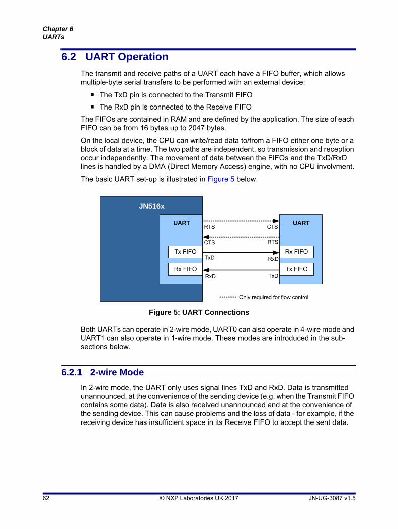
Chapter 6UARTs
6.2 UART Operation
The transmit and receive paths of a UART each have a FIFO buffer, which allows multiple-byte serial transfers to be performed with an external device:
The TxD pin is connected to the Transmit FIFO
The RxD pin is connected to the Receive FIFO
The FIFOs are contained in RAM and are defined by the application. The size of each FIFO can be from 16 bytes up to 2047 bytes.
On the local device, the CPU can write/read data to/from a FIFO either one byte or a block of data at a time. The two paths are independent, so transmission and reception occur independently. The movement of data between the FIFOs and the TxD/RxD lines is handled by a DMA (Direct Memory Access) engine, with no CPU involvment.
The basic UART set-up is illustrated in Figure 5 below.
Both UARTs can operate in 2-wire mode, UART0 can also operate in 4-wire mode and UART1 can also operate in 1-wire mode. These modes are introduced in the sub-sections below.
6.2.1 2-wire Mode
In 2-wire mode, the UART only uses signal lines TxD and RxD. Data is transmitted unannounced, at the convenience of the sending device (e.g. when the Transmit FIFO contains some data). Data is also received unannounced and at the convenience of the sending device. This can cause problems and the loss of data - for example, if the receiving device has insufficient space in its Receive FIFO to accept the sent data.
Figure 5: UART Connections
JN516x
UART
Rx FIFO
Tx FIFO
UART
Tx FIFO
Rx FIFO
RTS
CTS
RxD
TxD
TxD
RxD
CTS
RTS
Only required for flow control
62 © NXP Laboratories UK 2017 JN-UG-3087 v1.5

JN516x Integrated Peripherals APIUser Guide
6.2.2 4-wire Mode (with Flow Control) [UART0 Only]
In 4-wire mode, UART0 uses the signal lines TxD, RxD, RTS and CTS. This allows flow control to be implemented, which ensures that sent data can always be accepted. The general principle of flow control is described below.
The RTS and CTS lines are flags that are used to indicate when it is safe to transfer data between the devices. The RTS line on one device is connected to the CTS line on the other device.
The destination device dictates when the source device should send data to it, as follows:
When the destination device is ready to receive data, it asserts its RTS line to request the source device to send data. This may be when the Receive FIFO fill-level on the destination device falls below a pre-defined level and the FIFO becomes able to receive more data.
The assertion of the RTS line on the destination device is seen by the source device as the assertion of its CTS line. The source device is then able to send data from its Transmit FIFO.
Flow control operation is illustrated in Figure 6 below.
Figure 6: Example of UART Flow Control (UART0 Only)
UART UARTRTS
CTS
RxD
TxD
TxD
RxD
CTS
RTS
Tx FIFO
Tx FIFORx FIFO
Rx FIFO
UART UARTRTS
CTS
RxD
TxD
TxD
RxD
CTS
RTS
Tx FIFO
Tx FIFORx FIFO
Rx FIFO
UART UARTRTS
CTS
RxD
TxD
TxD
RxD
CTS
RTS
Tx FIFO
Tx FIFORx FIFO
Rx FIFO
RTS line is asserted when Rx FIFO fill-level falls below pre-defined level
Asserted CTS line means that data can be transmitted
Data is transmitted on TxD line
Data is received on RxD line
RTS line is cleared when Rx FIFO fill-level rises to pre-defined level
CTS line is cleared and data transmission is stopped
Destination Source
1 2
34
5 6
JN-UG-3087 v1.5 © NXP Laboratories UK 2017 63

Chapter 6UARTs
The Integrated Peripherals API provides functions for controlling and monitoring the RTS/CTS lines, allowing the application to implement the flow control algorithm manually. In practice, manual flow control can be a burden for a busy CPU, particularly when the UART is operating at a high baud-rate. For this reason, the API provides an Automatic Flow Control option in which the state of the RTS line is controlled directly by the Receive FIFO fill-level on the destination device. The implementations of manual and automatic flow control using the functions of Integrated Peripherals API are described in Section 6.5.
6.2.3 1-Wire Mode [UART1 Only]
In 1-wire mode, UART1 uses the TxD line to transmit data unannounced, at the convenience of the sending device. In this mode, data is not received and the RxD line is unused (so the associated DIO pin is available for another purpose).
6.3 Configuring the UARTs
This section describes the various aspects of configuring a UART before using it to transfer serial data.
6.3.1 Enabling a UART
A UART is enabled using the function bAHI_UartEnable(), which enables UART0 in 4-wire mode or UART1 in 2-wire mode, by default. This must be the first UART function called, unless you wish to use the UART in its non-default mode:
If you wish to use UART0 in 2-wire mode (without flow control), you will first need to call vAHI_UartSetRTSCTS() in order to release control of the DIOs used for the flow control RTS and CTS lines.
If you wish to use UART1 in 1-wire mode (transmit only), you will first need to call vAHI_UartTxOnly() in order to release control of the pin used for RxD.
The function bAHI_UartEnable() also allows the FIFO buffers for the UART transmit and receive paths to be configured. Each buffer is defined by the application as a section of RAM, and the start address and size (in bytes) of each buffer must be specified. The maximum possible buffer size is 2047 bytes and the minimum possible buffer size is 16 bytes.
Note: The function vAHI_UartEnable() (returns void rather than boolean) is also available for backward compatibility with application code developed for the JN514x microcontrollers.
64 © NXP Laboratories UK 2017 JN-UG-3087 v1.5
JN516x Integrated Peripherals APIUser Guide
6.3.2 Setting the Baud-rate
The following functions are provided for setting the baud-rate of a UART:
vAHI_UartSetBaudRate()
This function allows one of the following standard baud-rates to be set: 4800, 9600, 19200, 38400, 76800 or 115200 bps.
vAHI_UartSetBaudDivisor()
This function allows a 16-bit integer divisor (Divisor) to be specified which will be used to derive the baud-rate from a 1MHz frequency, given by:
vAHI_UartSetClocksPerBit()
This function can be used to obtain a more refined baud-rate than can be achieved using vAHI_UartSetBaudDivisor() alone. The divisor from the latter function is used in conjunction with an 8-bit integer parameter (Cpb) from vAHI_UartSetClocksPerBit() to derive a baud-rate from the 16MHz peripheral clock, given by:
Based on the above formula, the highest recommended baud-rate that can be achieved is 4Mbps (Divisor=1, Cpb=3).
6.3.3 Setting Other UART Properties
In addition to setting the baud-rate of a UART, as described in Section 6.3.2, it is also necessary to configure a number of other properties of the UART. These properties are set using the function vAHI_UartSetControl() and include the following:
Parity checks can be optionally applied to the transferred data and the type of parity (odd or even) can be selected.
The length of a word of data can be set to 5, 6, 7 or 8 bits - this is the number of bits per transmitted ‘character’ and should normally be set to 8 (a byte).
The number of stop bits can be set to 1 or 1.5 / 2.
The initial state of the RTS line can be configured (set or cleared) - this is only implemented if using UART0 in 4-wire mode (see Section 6.3.1).
Note: Either vAHI_UartSetBaudRate() or vAHI_UartSetBaudDivisor() must be called, but not both. If used, vAHI_UartSetClocksPerBit() must be called after vAHI_UartSetBaudDivisor().
1 106
Divisor--------------------
16 106
Divisor Cpb 1+ ---------------------------------------------------
JN-UG-3087 v1.5 © NXP Laboratories UK 2017 65

Chapter 6UARTs
6.3.4 Enabling Interrupts
UART interrupts can be generated under a variety of conditions. The interrupts can be enabled and configured using the function vAHI_UartSetInterrupt(). The possible interrupt conditions are as follows:
Transmit FIFO empty: The Transmit FIFO has become empty (and therefore requires more data).
Receive data available: The Receive FIFO has filled with data to a pre-defined level, which can be set to 1, 4, 8 or 14 bytes. This interrupt is cleared when the FIFO fill-level falls below the pre-defined level again.
Timeout: This interrupt is enabled when the ‘receive data available’ interrupt is enabled and is generated if all the following conditions exist:
At least one character is in the FIFO.
No character has entered the FIFO during a time interval in which at least four characters could potentially have been received.
Nothing has been read from the FIFO during a time interval in which at least four characters could potentially have been read.
A timeout interrupt is cleared and the timer is reset by reading a character from the Receive FIFO.
Receive line status: An error condition has occurred on the RxD line, such as a break indication, framing error, parity error or over-run.
Modem status: A change in the CTS line has been detected (for example, it has been asserted to indicate that the remote device is ready to accept data) in the case of UART0 operating 4-wire mode.
UART interrupts are handled by a callback function which must be registered using the function vAHI_Uart0RegisterCallback() or vAHI_Uart1RegisterCallback(), depending on the UART (0 or 1). For more information on UART interrupt handling, refer to Section 6.8.
66 © NXP Laboratories UK 2017 JN-UG-3087 v1.5
JN516x Integrated Peripherals APIUser Guide
6.4 Transferring Serial Data in 2-wire Mode
In 2-wire mode, a UART only uses signals RxD and TxD, and does not implement flow control. Data transmission and reception are covered separately below.
6.4.1 Transmitting Data (2-wire Mode)
Data is transmitted via a UART by calling one of the following functions:
vAHI_UartWriteData(): This function can be used to write a single byte of data to the Transmit FIFO. If used, this function may be called multiple times to queue data bytes for transmission.
u16AHI_UartBlockWriteData(): This function is used to write a block of data bytes to the Transmit FIFO. The function will return the number of bytes that have been successfully written to the FIFO.
Once in the FIFO, a data byte starts to be transmitted as soon as it reaches the head of the FIFO (and provided that the TxD line is idle). The transfer of data from the FIFO to the TxD line is handled automatically by the DMA engine.
The following methods can be used to prompt the application to call the vAHI_UartWriteData() or u16AHI_UartBlockWriteData() function:
The function u16AHI_UartReadTxFifoLevel() can be called to check the number of characters currently waiting in the Transmit FIFO (more data could then be written to the FIFO, if there is sufficient free space).
The function u8AHI_UartReadLineStatus() can be used to check whether the Transmit FIFO is empty.
An interrupt can be generated when the Transmit FIFO becomes empty (that is, when the last data byte in the FIFO starts to be transmitted) - this interrupt is enabled using the function vAHI_UartSetInterrupt().
A timer can be used to schedule periodic transmissions (provided that data is available to be transmitted).
Note 1: For UART1, 2-wire mode is the default mode.
Note 2: In order to operate UART0 in 2-wire mode, the function vAHI_UartSetRTSCTS() must first be called to release control of the DIOs used for flow control. This function must be called before vAHI_UartEnable().
JN-UG-3087 v1.5 © NXP Laboratories UK 2017 67
Chapter 6UARTs
6.4.2 Receiving Data (2-wire Mode)
Data is received on the RxD line as and when the source device sends it. The local transfer of data from the RxD line to the Receive FIFO is handled automatically by the DMA engine. The destination application can read data from the FIFO using one of the following functions:
u8AHI_UartReadData(): This function can be used to read a single byte of data from the Receive FIFO.
u16AHI_UartBlockReadData(): This function can be used to read a block of data bytes from the Receive FIFO.
The following methods can be used to prompt the application to call the u8AHI_UartReadData() or u16AHI_UartBlockReadData() function:
The function u16AHI_UartReadRxFifoLevel() can be called to check the number of characters currently in the Receive FIFO.
The function u8AHI_UartReadLineStatus() can be used to check whether the Receive FIFO contains data that can be read (or is empty).
An interrupt can be generated when the Receive FIFO contains a certain number of data bytes - this interrupt is enabled using the function vAHI_UartSetInterrupt(), in which the trigger level for the interrupt must be specified as 1, 4, 8 or 14 bytes.
A timer can be used to schedule periodic reads of the Receive FIFO. Before each timed read, the presence of data in the FIFO can be checked using either u8AHI_UartReadLineStatus() or u16AHI_UartReadRxFifoLevel().
Note: When the ‘receive data available’ interrupt is enabled (described above), a ‘timeout’ interrupt is also enabled for the Receive FIFO. For more details of this interrupt, refer to Section 6.3.4.
68 © NXP Laboratories UK 2017 JN-UG-3087 v1.5

JN516x Integrated Peripherals APIUser Guide
6.5 Transferring Serial Data in 4-wire Mode (UART0 Only)
In 4-wire mode, UART0 uses the signals RTS and CTS to implement flow control (see Section 6.2.2), as well as RxD and TxD. Flow control can be implemented manually by the application or automatically. The implementation of manual flow control is described below for transmission and reception separately, and then automatic flow control is described.
6.5.1 Transmitting Data (4-wire Mode, Manual Flow Control)
In the flow control protocol, the source device should only transmit data when the destination device is ready to receive (see Section 6.5.2). The readiness of the destination device to accept data is indicated on the source device by its CTS line being asserted. The status of the CTS line can be monitored in either of the following ways:
The source device can check the status of its CTS line using the function u8AHI_UartReadModemStatus().
An interrupt can be generated when a change in status of the CTS line occurs - this interrupt is enabled using the function vAHI_UartSetInterrupt().
Once a change in the state of the CTS line (to asserted) has been detected, one of the following functions can be called:
vAHI_UartWriteData(): This function can be used to write a single byte of data to the Transmit FIFO. If used, this function may be called multiple times to queue data bytes for transmission.
u16AHI_UartBlockReadData(): This function can be used to read a block of data bytes from the Receive FIFO. The function will return the number of bytes that have been successfully written to the FIFO.
Once in the FIFO, a data byte starts to be transmitted as soon as it reaches the head of the FIFO (and provided that the TxD line is idle). The transfer of data from the FIFO to the TxD line is handled automatically by the DMA engine.
Note that before calling vAHI_UartWriteData() to write data to the Transmit FIFO, the application may check whether there is already data in the FIFO (left over from a previous transfer) using the function u16AHI_UartReadTxFifoLevel() or u8AHI_UartReadLineStatus().
The CTS line is de-asserted when the RTS line is de-asserted on the destination device - see Section 6.5.2.
Note 1: 4-wire mode is the default mode on UART0. Therefore, the UART will automatically have control of the DIOs used for the RTS and CTS lines as soon as vAHI_UartEnable() is called.
Note 2: 4-wire mode is not available on UART1.
JN-UG-3087 v1.5 © NXP Laboratories UK 2017 69

Chapter 6UARTs
6.5.2 Receiving Data (4-wire Mode, Manual Flow Control)
In the flow control protocol, the destination device should only receive data when it is ready. This is normally when its Receive FIFO has sufficient free space to accept more data. The application can check the fill status of its Receive FIFO using the function u16AHI_UartReadRxFifoLevel() or u8AHI_UartReadLineStatus().
Once the application on the destination device has decided that it is ready to receive data, it must request the data from the source device by asserting the RTS line (which asserts the CTS line on the source device - see Section 6.5.1). The RTS line can be asserted using the function vAHI_UartSetRTS() or vAHI_UartSetControl().
The source device may then send data, which is received on the RxD line on the destination device. The local transfer of data from the RxD line to the Receive FIFO is handled automatically by the DMA engine. The received data can be read from the Receive FIFO using one of the following functions:
u8AHI_UartReadData(): This function can be used to read a single byte of data from the Receive FIFO.
u16AHI_UartBlockReadData(): This function can be used to read a block of data bytes from the Receive FIFO.
The application may subsequently make a decision to stop the transfer from the source device, which is achieved by de-asserting the RTS line using the function vAHI_UartSetRTS() or vAHI_UartSetControl(). This decision is based on the fill-level of the Receive FIFO - when the amount of data in the FIFO reaches a certain level, the application will start to read the data and may also stop the transfer if it cannot read from the FIFO quickly enough to prevent an overflow condition. The current fill-level of the Receive FIFO can be monitored using either of the following mechanisms:
The function u16AHI_UartReadRxFifoLevel() can be called to check the number of data bytes currently in the Receive FIFO.
A ‘receive data available’ interrupt can be generated when the number of data bytes in the Receive FIFO rises to a certain level - this interrupt is enabled using the function vAHI_UartSetInterrupt(), in which the trigger-level for the interrupt must be specified as 1, 4, 8 or 14 bytes.
Note: When the ‘receive data available’ interrupt is enabled (described above), a ‘timeout’ interrupt is also enabled for the Receive FIFO. For more details of this interrupt, refer to Section 6.3.4.
70 © NXP Laboratories UK 2017 JN-UG-3087 v1.5

JN516x Integrated Peripherals APIUser Guide
6.5.3 Automatic Flow Control (4-wire Mode)
Flow control can be implemented automatically in UART0 4-wire mode, rather than manually (as described in Section 6.5.1 and Section 6.5.2). Automatic flow control can be used on the destination device and/or on the source device:
On the destination device, automatic flow control avoids the need for the application to monitor the Receive FIFO fill-level and to assert/de-assert the RTS line.
On the source device, automatic flow control avoids the need for the application to monitor the CTS line before transmitting data.
Automatic flow control is configured and enabled using the function vAHI_UartSetAutoFlowCtrl() which, if used, must be called after enabling the UART and before starting the data transfer.
The vAHI_UartSetAutoFlowCtrl() function allows:
A Receive FIFO trigger-level to be specified on the destination device (as 8, 11, 13 or 15 bytes), so that:
The local RTS line is asserted when the fill-level is below the trigger-level, indicating the readiness of the destination device to accept more data.
The local RTS line is de-asserted when the fill-level is at or above the trigger-level, indicating that the destination device is not in a position to accept more data.
Thus, as the destination Receive FIFO fill-level rises and falls (as data is received and read), the local RTS line is automatically manipulated to control the arrival of further data from the source device.
Automatic monitoring of the CTS line to be enabled on the source device - when this line is asserted, any data in the Transmit FIFO is transmitted automatically.
This function also allows the RTS/CTS signals to be configured as active-high or active-low.
Automatic flow control can be set up between the two devices either for data transfers in only one direction or for data transfers in both directions.
Although much of the data transfer is automatic, the application on the source device must write data into its Transmit FIFO and the application on the destination device must read data from its Receive FIFO. These operations are described below.
JN-UG-3087 v1.5 © NXP Laboratories UK 2017 71
Chapter 6UARTs
Transmitting Data
To transmit data, the sending application can use one of the following functions:
vAHI_UartWriteData(): This function can be used to write a single byte of data to the Transmit FIFO. If used, this function may be called multiple times to queue data bytes for transmission.
u16AHI_UartBlockReadData(): This function can be used to read a block of data bytes from the Receive FIFO. The function will return the number of bytes that have been successfully written to the FIFO.
Once in the FIFO, the data is automatically transmitted (via the TxD line) as soon as the CTS line indicates that the destination device is ready to receive. The transfer of data from the FIFO to the TxD line is handled automatically by the DMA engine.
Note that before calling vAHI_UartWriteData() or u16AHI_UartBlockReadData() to write data to the Transmit FIFO, the application may check whether there is already data in the FIFO (left over from a previous transfer) using the function u8AHI_UartReadTxFifoLevel() or u8AHI_UartReadLineStatus().
Receiving Data
Data is received on the RxD line on the destination device. The local transfer of data from the RxD line to the Receive FIFO is handled automatically by the DMA engine. The received data can be read from the Receive FIFO using one of the following functions:
u8AHI_UartReadData(): This function can be used to read a single byte of data from the Receive FIFO.
u16AHI_UartBlockReadData(): This function can be used to read a block of data bytes from the Receive FIFO.
The application can decide when to start and stop reading data from the Receive FIFO, based on either of the following mechanisms:
The function u16AHI_UartReadRxFifoLevel() can be called to check the number of characters currently in the Receive FIFO. Thus, the application may decide to start reading data when the FIFO fill-level is at or above a certain threshold. It may decide to stop reading data when the FIFO fill-level is at or below another threshold, or when the FIFO is empty.
A ‘receive data available’ interrupt can be generated when the Receive FIFO contains a certain number of data bytes - this interrupt is enabled using the function vAHI_UartSetInterrupt(), in which the trigger-level for the interrupt must be specified as 1, 4, 8 or 14 bytes. Thus, the application may decide to start reading data from the Receive FIFO when this interrupt occurs and to stop reading data when all the received bytes have been extracted from the FIFO.
Note: When the ‘receive data available’ interrupt is enabled (described above), a ‘timeout’ interrupt is also enabled for the Receive FIFO. For more details of this interrupt, refer to Section 6.3.4.
72 © NXP Laboratories UK 2017 JN-UG-3087 v1.5

JN516x Integrated Peripherals APIUser Guide
6.6 Transmitting Serial Data in 1-wire Mode (UART1 Only)
In 1-wire mode, UART1 uses only the TxD line and can only transmit serial data. This transmission is performed at the convenience of the sending device (so no flow control is implemented).
For this mode, the function vAHI_UartTxOnly() must be called to release control of the pin used for RxD before the UART is enabled using bAHI_UartEnable(). Since the RxD line is not used and the Receive FIFO buffer is therefore not needed, in bAHI_UartEnable() you are advised to set the pointer to the start of this buffer in RAM to NULL - this avoids allocating RAM space to this buffer.
6.7 Break Condition
During a data transfer, if the application on this source device becomes aware of an error, it can convey this error status to the destination device by setting a break condition using the function vAHI_UartSetBreak(). When this break condition is issued, the data byte that is currently being transmitted is corrupted and the transmission is stopped.
If a JN516x device receives a break condition (as the destination device), this results in a ‘receive line status’ interrupt (E_AHI_UART_INT_RXLINE) being generated on the device, provided that UART interrupts are enabled on this device. UART interrupts are described in Section 6.3.4 and UART interrupt handling in Section 6.8.
The vAHI_UartSetBreak() function can also be used to clear the break condition (from the source device). In this case, the transmission will restart in order to transfer the data remaining in the Transmit FIFO.
6.8 UART Interrupt Handling
Interrupts can be employed in a number of ways in controlling UART operation. The various uses of UART interrupts are introduced in Section 6.3.4 and are further covered in the sections on transferring data (Section 6.4 and Section 6.5).
UART interrupts are handled by a user-defined callback function, which must be registered using vAHI_Uart0RegisterCallback() or vAHI_Uart1RegisterCallback(), depending on the UART (0 or 1). The relevant callback function is automatically invoked when an interrupt of the type E_AHI_DEVICE_UART0 (for UART 0) or E_AHI_DEVICE_UART1 (for UART 1) occurs. For details of the callback function prototype, refer to Appendix A.1.
Caution: The registered callback function is only preserved during sleep modes in which RAM remains powered. If RAM is powered off during sleep and interrupts are required, the callback function must be re-registered before calling u32AHI_Init() on waking.
JN-UG-3087 v1.5 © NXP Laboratories UK 2017 73
Chapter 6UARTs
The exact nature of the UART interrupt (from those listed in Section 6.3.4) can then be identified from an enumeration that is passed into the callback function. For details of these enumerations, refer to Appendix B.2.
Note that the handling of UART interrupts differs from the handling of other interrupts in the following ways:
The exact cause of an interrupt is normally indicated to the callback function by means of a bitmap, but not in the case of a UART interrupt - instead, an enumeration is used to indicate the nature of a UART interrupt. The reported enumeration corresponds to the currently active interrupt condition with the highest priority.
An interrupt is normally automatically cleared before the callback function is invoked, but the UARTs are the exception to this rule. When generating a 'receive data available' or 'timeout' interrupt, the UART will only clear the interrupt once the data has been read from the Receive FIFO. It is therefore vital that the callback function handles the UART 'receive data available' and 'timeout' interrupts by reading the data from the Receive FIFO before returning.
Note: If the Application Queue API is being used, the above issue with the UART interrupts is handled by this API, so the application does not need to deal with it. For more information on this API, refer to the IEEE 802.15.4 Stack User Guide (JN-UG-3024).
74 © NXP Laboratories UK 2017 JN-UG-3087 v1.5

JN516x Integrated Peripherals APIUser Guide
7. Timers
This chapter describes control of the on-chip timers using functions of the Integrated Peripherals API. On the JN516x device, there are five timers: Timer 0, Timer 1, Timer 2, Timer 3 and Timer 4.
The timers offer a range of operating modes:
Timer mode
Pulse Width Modulation (PWM) mode
Counter mode
Capture mode
Delta-Sigma mode
However, not all the timers can operate in all modes. Timers 1-4 do not support modes that require external inputs - these are Counter mode and Capture mode. The timer modes are outlined in Section 7.1.
To use a timer in one of the above modes:
1. First refer to Section 7.2 on setting up a timer.
2. Then refer to Section 7.3 on operating a timer (you should refer to the sub-section which corresponds to your chosen mode of operation).
For information on Timer interrupts, refer to Section 7.4.
Note: These timers are distinct from the wake timers described in Chapter 8 and tick timer described in Chapter 9.
JN-UG-3087 v1.5 © NXP Laboratories UK 2017 75

Chapter 7Timers
7.1 Modes of Timer Operation
The following timer modes are available on the JN516x microcontrollers: Timer, Pulse Width Modulation (PWM), Counter, Capture and Delta-Sigma. These modes are summarised in the table below, along with the functions needed for each mode (following a call to vAHI_TimerEnable()). A mode is supported by all JN516x timers unless otherwise stated.
Mode Description Functions
Timer The source clock is used to produce a pulse cycle defined by the number of clock cycles until a positive pulse edge and until a negative pulse edge. Inter-rupts can be generated on either or both edges. The pulse cycle can be produced just once in ‘single-shot’ mode or continuously in ‘repeat’ mode. Timer mode is described further in Section 7.3.1.
vAHI_TimerConfigureOutputs()
vAHI_TimerStartSingleShot() or vAHI_TimerStartRepeat()
PWM As for Timer mode, except the Pulse Width Modu-lated signal is output on a DIO pin (which depends on the specific timer used - see Section 7.2.1). PWM mode is described further in Section 7.3.1.
vAHI_TimerConfigureOutputs()
vAHI_TimerStartSingleShot() or vAHI_TimerStartRepeat()
Counter The timer is used to count edges on an external input signal, selected as an external clock input. The timer can count just rising edges or both rising and falling edges. Counter mode is described further in Section 7.3.4.
Supported by Timer 0 but not by Timers 1-4
vAHI_TimerClockSelect()
vAHI_TimerConfigureInputs()
vAHI_TimerStartSingleShot() or vAHI_TimerStartRepeat()
u16AHI_TimerReadCount()
Capture An external input signal is sampled on every tick of the source clock. The results of the capture allow the period and pulse width of the sampled signal to be calculated. If required, the results can be read with-out stopping the timer. Capture mode is described further in Section 7.3.3.
Supported by Timer 0 but not by Timers 1-4
vAHI_TimerConfigureInputs()
vAHI_TimerStartCapture()
vAHI_TimerReadCapture() or vAHI_TimerReadCaptureFreeRunning()
Delta-Sigma The timer is used as a low-rate DAC. The converted signal is output on a DIO pin (which depends on the specific timer used - see Section 7.2.1) and requires simple filtering to give the analogue signal. Delta-Sigma mode is available in two options, NRZ and RTZ, and is described further in Section 7.3.2.
vAHI_TimerStartDeltaSigma()
Table 2: Modes of Timer Operation
76 © NXP Laboratories UK 2017 JN-UG-3087 v1.5
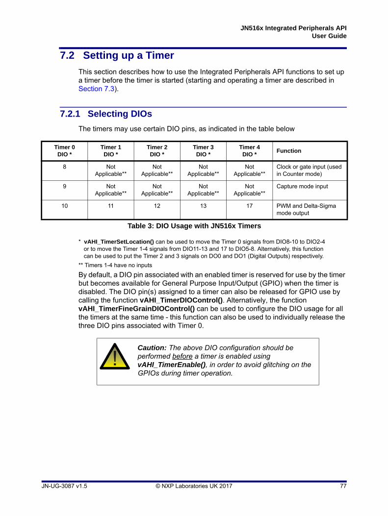
JN516x Integrated Peripherals APIUser Guide
7.2 Setting up a Timer
This section describes how to use the Integrated Peripherals API functions to set up a timer before the timer is started (starting and operating a timer are described in Section 7.3).
7.2.1 Selecting DIOs
The timers may use certain DIO pins, as indicated in the table below
* vAHI_TimerSetLocation() can be used to move the Timer 0 signals from DIO8-10 to DIO2-4 or to move the Timer 1-4 signals from DIO11-13 and 17 to DIO5-8. Alternatively, this function can be used to put the Timer 2 and 3 signals on DO0 and DO1 (Digital Outputs) respectively.
** Timers 1-4 have no inputs
By default, a DIO pin associated with an enabled timer is reserved for use by the timer but becomes available for General Purpose Input/Output (GPIO) when the timer is disabled. The DIO pin(s) assigned to a timer can also be released for GPIO use by calling the function vAHI_TimerDIOControl(). Alternatively, the function vAHI_TimerFineGrainDIOControl() can be used to configure the DIO usage for all the timers at the same time - this function can also be used to individually release the three DIO pins associated with Timer 0.
Timer 0 DIO *
Timer 1 DIO *
Timer 2 DIO *
Timer 3 DIO *
Timer 4 DIO *
Function
8 Not Applicable**
Not Applicable**
Not Applicable**
Not Applicable**
Clock or gate input (used in Counter mode)
9 Not Applicable**
Not Applicable**
Not Applicable**
Not Applicable**
Capture mode input
10 11 12 13 17 PWM and Delta-Sigma mode output
Table 3: DIO Usage with JN516x Timers
Caution: The above DIO configuration should be performed before a timer is enabled using vAHI_TimerEnable(), in order to avoid glitching on the GPIOs during timer operation.
JN-UG-3087 v1.5 © NXP Laboratories UK 2017 77

Chapter 7Timers
7.2.2 Enabling a Timer
Before a timer can be started, it must be configured and enabled using the function vAHI_TimerEnable().
The vAHI_TimerEnable() function contains certain configuration parameters, which are outlined below.
Clock Divisor:
To obtain the timer frequency, the peripheral clock is divided by a factor of 2prescale, where prescale is a user-configurable integer value in the range 0 to 16 (note that the value 0 leaves the clock frequency unchanged). For example, for a 16MHz peripheral clock and a prescale value of 3, a division factor of 8 is used to give a timer frequency of 2MHz. A system clock sourced from the external crystal oscillator will give the most stable timer frequency (for system clock options, refer to Section 3.1).
Interrupts:
Each timer can be configured to generate interrupts on either or both of the following conditions:
On the rising edge of the timer output (at end of low period)
On the falling edge of the timer output (at the end of full timer period)
Timer interrupts are further described in Section 7.4.
External Output:
The timer signal can be output externally, but this output must be explicitly enabled. This output is required for Delta-Sigma mode and PWM mode. It is this option which distinguishes between Timer mode (output disabled) and PWM mode (output enabled). The DIO pin on which the timer signal is output depends on the device type:
For Timer 0, DIO10 is used
For Timer 1, DIO11 is used
For Timer 2, DIO12 is used
For Timer 3, DIO13 is used
For Timer 4, DIO17 is used
Once a timer has been enabled using vAHI_TimerEnable(), an external clock input can be selected (if required - see Section 7.2.3) and then the timer can be started in the desired mode using the relevant start function (see Section 7.3.1 to Section 7.3.4).
Caution: You must enable a timer before attempting any other operation on it, otherwise an exception may result.
78 © NXP Laboratories UK 2017 JN-UG-3087 v1.5

JN516x Integrated Peripherals APIUser Guide
7.2.3 Selecting Clocks
Each timer requires a source clock, which is provided by the peripheral clock. This source clock is divided down to produce the timer’s clock. The division factor is specified when the timer is enabled using vAHI_TimerEnable() - see Section 7.2.2. A system clock sourced from the external crystal oscillator gives the most stable timer frequency (for system clock options, refer to Section 3.1).
When Timer 0 is operating in Counter mode (see Section 7.3.4), an external clock is monitored by the timer. This signal is input on the DIO8 pin and this input must be enabled using the function vAHI_TimerClockSelect(), which must be called after vAHI_TimerEnable().
Note: An enabled timer can be disabled using the function vAHI_TimerDisable(). This stops the timer (if running) and powers down the timer block - this is useful to reduce power consumption when the timer is not needed. The application must not attempt to access a disabled timer, otherwise an exception may occur.
JN-UG-3087 v1.5 © NXP Laboratories UK 2017 79
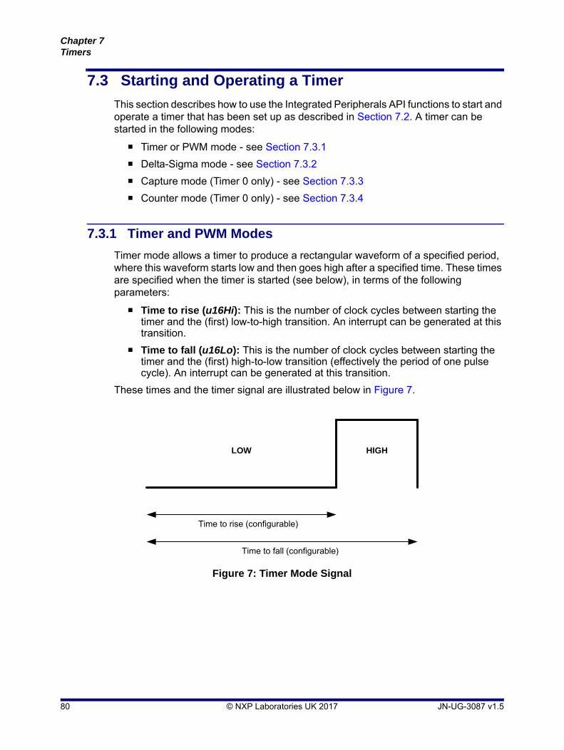
Chapter 7Timers
7.3 Starting and Operating a Timer
This section describes how to use the Integrated Peripherals API functions to start and operate a timer that has been set up as described in Section 7.2. A timer can be started in the following modes:
Timer or PWM mode - see Section 7.3.1
Delta-Sigma mode - see Section 7.3.2
Capture mode (Timer 0 only) - see Section 7.3.3
Counter mode (Timer 0 only) - see Section 7.3.4
7.3.1 Timer and PWM Modes
Timer mode allows a timer to produce a rectangular waveform of a specified period, where this waveform starts low and then goes high after a specified time. These times are specified when the timer is started (see below), in terms of the following parameters:
Time to rise (u16Hi): This is the number of clock cycles between starting the timer and the (first) low-to-high transition. An interrupt can be generated at this transition.
Time to fall (u16Lo): This is the number of clock cycles between starting the timer and the (first) high-to-low transition (effectively the period of one pulse cycle). An interrupt can be generated at this transition.
These times and the timer signal are illustrated below in Figure 7.
Figure 7: Timer Mode Signal
Time to rise (configurable)
Time to fall (configurable)
LOW HIGH
80 © NXP Laboratories UK 2017 JN-UG-3087 v1.5

JN516x Integrated Peripherals APIUser Guide
Within Timer mode, there are two sub-modes and the timer is started in these modes using different functions:
Single-shot mode: The timer produces a single pulse cycle (as depicted in Figure 7) and then stops. The timer can be started in this mode using vAHI_TimerStartSingleShot().
Repeat mode: The timer produces a train of pulses (where the repetition rate is determined by the configured ‘time to fall’ period - see above). The timer can be started in this mode using vAHI_TimerStartRepeat().
Once started, the timer can be stopped using the function vAHI_TimerStop().
PWM (Pulse Width Modulation) mode is identical to Timer mode except the produced waveform is output on a DIO pin - see Section 7.2.1 for the relevant DIOs. This output can be enabled in vAHI_TimerEnable(). The output can also be inverted using the function vAHI_TimerConfigureOutputs().
7.3.2 Delta-Sigma Mode (NRZ and RTZ)
Delta-Sigma mode allows a timer to be used as a simple low-rate DAC. This requires the timer output on a DIO pin to be enabled in the call to vAHI_TimerEnable() - see Section 7.2.1 for the relevant DIOs. An RC (Resistor-Capacitor) circuit must be inserted between this pin and Ground (see Figure 8).
A timer is started in Delta-Sigma mode using vAHI_TimerStartDeltaSigma(). The value to be converted is digitally encoded by the timer as a pseudo-random waveform in which:
the total number of clock cycles that make up one period of the waveform is fixed (at 216 for NRZ and at 217 for RTZ - see below)
the number of high clock cycles during one period is set to a number which is proportional to the value to be converted
the high clock cycles are distributed randomly throughout a complete period
Thus, the capacitor will charge in proportion to the specified value such that, at the end of the period, the voltage produced is an analogue representation of the digital value. The output voltage requires calibration - for example, you could determine the maximum possible voltage by measuring the voltage across the capacitor after a conversion with the high period set to the whole pulse period (less one clock cycle).
Two Delta-Sigma mode options are available, NRZ and RTZ:
NRZ (Non Return-to-Zero): Delta-Sigma NRZ mode uses the 16MHz peripheral clock and the period of the waveform is fixed at 216 clock cycles. The NRZ option means that clock cycles are implemented without gaps between them (see RTZ option below). You must define the number of clock cycles spent in the high state during the pulse cycle such that this high period is proportional to the value to be converted. This number is set when the timer is started using the function vAHI_TimerStartDeltaSigma(). For example, if you wish to convert values in the range 0-100 then 216 clock cycles would correspond to 100, and to convert the value 25 you must set the number of high
JN-UG-3087 v1.5 © NXP Laboratories UK 2017 81

Chapter 7Timers
clock cycles to 214 (a quarter of the pulse cycle). For an illustration, refer to Figure 8.
RTZ (Return-to-Zero): Delta-Sigma RTZ mode is similar to the NRZ option, described above, except that after every clock cycle, a blank (low) clock cycle is inserted. Thus, each pulse cycle takes twice as many clock cycles - that is, 217. Note that this does not affect the required number of high clock cycles to represent the digital value being converted. This mode doubles the conversion period but improves linearity if the rise and fall times of the outputs are different from each other.
7.3.3 Capture Mode
Capture mode is available on Timer 0 only (and not on Timers 1-4). In this mode, the timer can be used to measure the pulse width of an external input. The external signal must be provided on a DIO pin - see Section 7.2.1 for the relevant DIOs. The timer measures the number of clock cycles in the input signal from the start of capture to the next low-to-high transition and also to next the high-to-low transition. The number of clock cycles in the last pulse is then the difference between these measured values (see Figure 9). The pulse width in units of time is then given by:
Pulse width (in units of time) = Number of clock cycles in pulse X Clock cycle period
A timer is started in Capture mode using the function vAHI_TimerStartCapture(). The timer can be stopped and the most recent measurements obtained using the function
Note: For more information on ‘Delta-Sigma’ mode, refer to the data sheet for your microcontroller.
Figure 8: Delta-Sigma NRZ Mode Operation
R
C
DIO
Period(216 clock cycles, e.g. corresponding to 100)
High periods represent value, e.g. 214 clock cycles corresponding to 25
JN516x Timer in Delta-Sigma Mode
Vout
82 © NXP Laboratories UK 2017 JN-UG-3087 v1.5
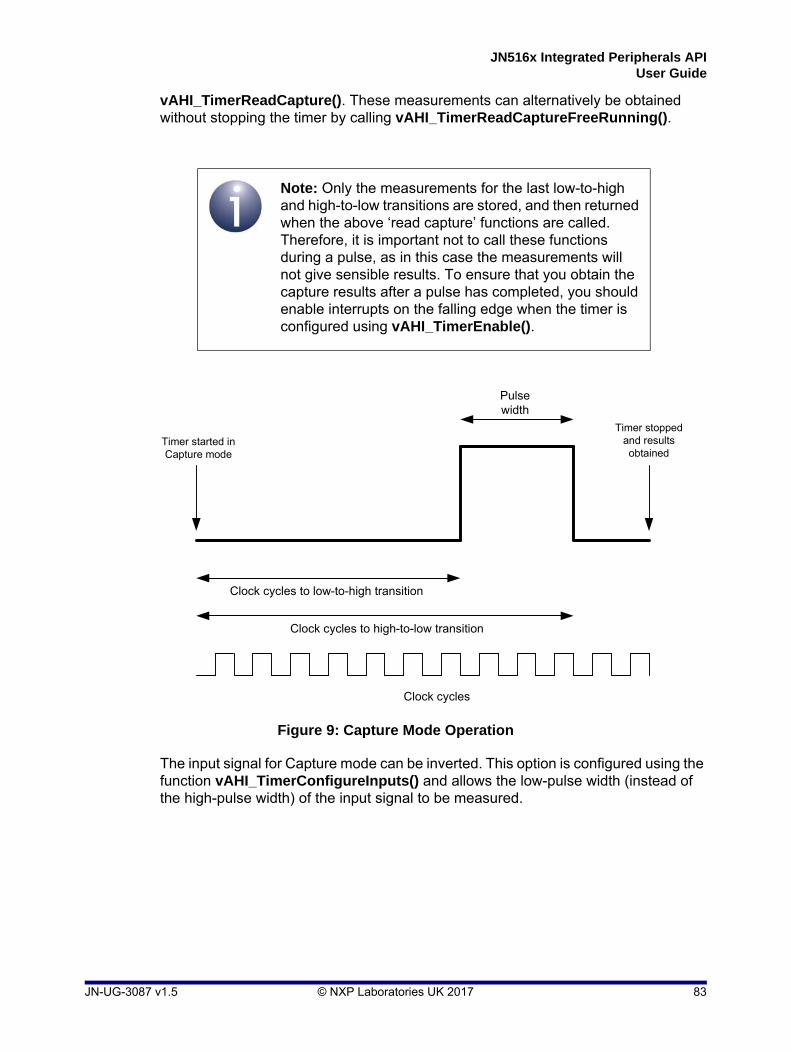
JN516x Integrated Peripherals APIUser Guide
vAHI_TimerReadCapture(). These measurements can alternatively be obtained without stopping the timer by calling vAHI_TimerReadCaptureFreeRunning().
The input signal for Capture mode can be inverted. This option is configured using the function vAHI_TimerConfigureInputs() and allows the low-pulse width (instead of the high-pulse width) of the input signal to be measured.
Note: Only the measurements for the last low-to-high and high-to-low transitions are stored, and then returned when the above ‘read capture’ functions are called. Therefore, it is important not to call these functions during a pulse, as in this case the measurements will not give sensible results. To ensure that you obtain the capture results after a pulse has completed, you should enable interrupts on the falling edge when the timer is configured using vAHI_TimerEnable().
Figure 9: Capture Mode Operation
Clock cycles to low-to-high transition
Clock cycles to high-to-low transition
Pulse width
Timer started in Capture mode
Timer stoppedand resultsobtained
Clock cycles
JN-UG-3087 v1.5 © NXP Laboratories UK 2017 83

Chapter 7Timers
7.3.4 Counter Mode
Counter mode is available on Timer 0 only (and not on Timers 1-4). In this mode, the timer counts edges on an external clock signal, which must be provided on a DIO pin - see Section 7.2.1 for the relevant DIOs. Counter mode is enabled by selecting an external clock input in a call to vAHI_TimerClockSelect().
The timer can count rising edges only or both rising and falling edges. This must be configured using the function vAHI_TimerConfigureInputs(). Edges must be at least 100ns apart, i.e. pulses must be wider than 100ns.
Like Timer/PWM mode, the timer can then be started in one of two sub-modes:
Single-shot mode: The timer can be started in this mode using the function vAHI_TimerStartSingleShot() and will stop at a specified count value (u16Lo).
Repeat mode: The timer can be started in this mode using the function vAHI_TimerStartRepeat(). The timer operates continuously and the counter resets to zero each time the specified count value (u16Lo) is reached.
The above start functions each allow two counts to be specified at which interrupts will be generated (timer interrupts must also have been enabled in vAHI_TimerEnable()).
The current count of a running timer can be obtained at any time using the function u16AHI_TimerReadCount(). The timer can be stopped using vAHI_TimerStop().
84 © NXP Laboratories UK 2017 JN-UG-3087 v1.5

JN516x Integrated Peripherals APIUser Guide
7.4 Timer Interrupts
A timer can be configured in vAHI_TimerEnable() to generate interrupts on either or both of the following conditions:
On the rising edge of the timer output (at end of low period)
On the falling edge of the timer output (at the end of full timer period)
The handling of timer interrupts must be incorporated in a user-defined callback function for the particular timer. These callback functions are registered using dedicated registration functions for the individual timers:
vAHI_Timer0RegisterCallback() for Timer 0
vAHI_Timer1RegisterCallback() for Timer 1
vAHI_Timer2RegisterCallback() for Timer 2
vAHI_Timer3RegisterCallback() for Timer 3
vAHI_Timer4RegisterCallback() for Timer 4
The relevant callback function is automatically invoked when an interrupt of the type E_AHI_DEVICE_TIMER0, E_AHI_DEVICE_TIMER1, E_AHI_DEVICE_TIMER2, E_AHI_DEVICE_TIMER3 or E_AHI_DEVICE_TIMER4 occurs. The exact nature of the interrupt (from the two conditions listed above) can then be identified from a bitmap that is passed into the function. Note that the interrupt will be automatically cleared before the callback function is invoked.
Note: The callback function prototype is detailed in Appendix A.1. The interrupt source information is provided in Appendix B.
Caution: A registered callback function is only preserved during sleep modes in which RAM remains powered. If RAM is powered off during sleep and interrupts are required, the callback function must be re-registered before calling u32AHI_Init() on waking.
JN-UG-3087 v1.5 © NXP Laboratories UK 2017 85

Chapter 7Timers
86 © NXP Laboratories UK 2017 JN-UG-3087 v1.5
JN516x Integrated Peripherals APIUser Guide
8. Wake Timers
This chapter describes control of the on-chip wake timers using functions of the Integrated Peripherals API.
The JN516x microcontroller includes two wake timers, denoted Wake Timer 0 and Wake Timer 1, where each is a 41-bit counter. The wake timers are based on the 32kHz clock (which can be sourced internally or externally, as described in Section 3.1.5) and can run while the device is in sleep mode (and while the CPU is running). They are generally used to time the sleep duration and wake the device at the end of the sleep period. A wake timer counts down from a programmed value and wakes the device when the count reaches zero by generating an interrupt or wake-up event.
8.1 Using a Wake Timer
This section describes how to use the Integrated Peripherals API functions to operate a wake timer.
8.1.1 Enabling and Starting a Wake Timer
A wake timer is enabled using the function vAHI_WakeTimerEnable(). This function allows the interrupt to be enabled/disabled that is generated when the counter reaches zero. Note that wake timer interrupts are handled by the callback function registered using the function vAHI_SysCtrlRegisterCallback() - see Section 3.5.
A wake timer can then be started using the function vAHI_WakeTimerStartLarge(). This function takes as a parameter the starting value for the countdown - this value must be specified in 32kHz clock periods (thus, 32 corresponds to 1 millisecond).
On reaching zero, the timer ‘fires’, rolls over to 0x1FFFFFFFFFF and continues to count down. If enabled, the wake timer interrupt is generated on reaching zero.
Note: If the 32kHz clock is sourced from the (default) internal 32kHz RC oscillator, the wake timers may run up to 18% fast or slow. For more accurate timings, you are advised to first calibrate the clock and adjust the specified count value accordingly, as described in Section 8.2.
JN-UG-3087 v1.5 © NXP Laboratories UK 2017 87

Chapter 8Wake Timers
8.1.2 Stopping a Wake Timer
A wake timer can be stopped at any time using the function vAHI_WakeTimerStop(). The counter will then remain at the value at which it was stopped and will not generate an interrupt.
8.1.3 Reading a Wake Timer
The current count of a wake timer can be obtained using the function u64AHI_WakeTimerReadLarge(). This function does not stop the wake timer.
8.1.4 Obtaining Wake Timer Status
The states of the wake timers can be obtained using the following functions:
u8AHI_WakeTimerStatus() can be used to find out which wake timers are currently running.
u8AHI_WakeTimerFiredStatus() can be used to find out which wake timers have fired (passed zero). The ‘fired’ status of a wake timer is also cleared by this function.
8.2 Clock Calibration
The wake timers are driven by the JN516x microcontroller’s 32kHz clock. If this clock is sourced from the internal 32kHz RC oscillator, it may run up to 40% fast or 10% slow on the JN5169 device and up to 18% fast or slow on the other JN516x devices, depending on temperature, supply voltage and manufacturing tolerance. To achieve more accurate timings in this case, the self-calibration facility should be used that compares the 32kHz clock against the faster and more accurate peripheral clock, which should be running at 16MHz with the system clock sourced from the external crystal oscillator (for system clock information, refer to Section 3.1). This test is performed using Wake Timer 0. The result of this calibration allows you to calculate the required number of 32kHz clock cycles to achieve the desired timer duration when starting a wake timer with the function vAHI_WakeTimerStartLarge().
Note 1: If using u8AHI_WakeTimerFiredStatus() to check whether a wake timer caused a wake-up event, you must call this function before u32AHI_Init().
Note 2: If using the JenNet protocol, do not call u8AHI_WakeTimerFiredStatus() to obtain the wake timer interrupt status on waking from sleep. At wake-up, JenNet calls u32AHI_Init() internally and clears the interrupt status before passing control to the application. The System Controller callback function must be used to obtain the interrupt status, if required.
88 © NXP Laboratories UK 2017 JN-UG-3087 v1.5

JN516x Integrated Peripherals APIUser Guide
The calibration is performed using the function u32AHI_WakeTimerCalibrate(), as described below.
1. Wake Timer 0 must be disabled (using vAHI_WakeTimerStop(), if required).
2. The status of both wake timers (0 and 1) must be cleared by calling the function u8AHI_WakeTimerFiredStatus().
3. The calibration is started using u32AHI_WakeTimerCalibrate().
This causes Wake Timer 0 to start counting down 20 clock periods of the internal 32kHz clock. At the same time, a reference counter starts counting up from zero using the 16MHz peripheral clock.
4. When the wake timer reaches zero, u32AHI_WakeTimerCalibrate() returns the number of 16MHz clock cycles registered by the reference counter. Let this value be n.
If the clock is running at 32kHz, n = 10000
If the clock is running slower than 32kHz, n > 10000
If the clock is running faster than 32kHz, n < 10000
5. You can then calculate the required number of 32kHz clock periods (for vAHI_WakeTimerStartLarge()) to achieve the desired timer duration. If T is the required duration in seconds, the appropriate number of 32kHz clock periods, N, is given by:
For example, if a value of 9000 is obtained for n, this means that the 32kHz clock is running fast. Therefore, to achieve a 2 second timer duration, instead of requiring 64000 clock periods, you will need (10000/9000) x 32000 x 2 clock periods; that is, 71111 (rounded down).
Tip: To ensure that the device wakes in time for a scheduled event, it is better to under-estimate the required number of 32kHz clock periods than to over-estimate them.
N10000
n--------------- 32000 T=
JN-UG-3087 v1.5 © NXP Laboratories UK 2017 89

Chapter 8Wake Timers
90 © NXP Laboratories UK 2017 JN-UG-3087 v1.5
JN516x Integrated Peripherals APIUser Guide
9. Tick Timer
This chapter describes control of the Tick Timer using functions of the Integrated Peripherals API.
The Tick Timer is a hardware timer derived from the peripheral clock and can be used to implement:
timing interrupts to software
regular events, such as ticks for software timers or an operating system
a high-precision timing reference
system monitor timeouts, as used in a watchdog timer
9.1 Tick Timer Operation
The Tick Timer counts upwards until the count matches a pre-defined reference value (the starting value can be specified). The timer can be operated in one of three modes, which determine what the timer will do once the reference count has been reached. The options are:
Continue counting upwards
Restart the count from zero
Stop counting (single-shot mode)
An interrupt can also be enabled which is generated on reaching the reference count.
Note: For high-precision Tick Timer operation, the peripheral clock should run at 16MHz with the system clock sourced from the external crystal oscillator. For system clock information, refer to Section 3.1.
JN-UG-3087 v1.5 © NXP Laboratories UK 2017 91
Chapter 9Tick Timer
9.2 Using the Tick Timer
This section describes how to use the Integrated Peripherals API functions to set up and run the Tick Timer.
9.2.1 Setting Up the Tick Timer
On device power-up/reset, the Tick Timer is disabled. However, before setting up the Tick Timer, you are advised to call the function vAHI_TickTimerConfigure() and specify the disable option. The starting count and reference count can then be set as follows:
1. The starting count is set (in the range 0 to 0xFFFFFFFF) using the function vAHI_TickTimerWrite(). Note that if this function is called while the timer is enabled, the timer will immediately start counting from the specified value.
2. The reference count is set (in the range 0 to 0x0FFFFFFF) using the function vAHI_TickTimerInterval().
9.2.2 Running the Tick Timer
Once the timer has been set up (as described in Section 9.2.1), it can be started by calling the function vAHI_TickTimerConfigure() again but, this time, specifying one of the three operational modes listed in Section 9.1.
The current count of the Tick Timer can be obtained at any time by calling the function u32AHI_TickTimerRead().
Note that if the Tick Timer is started in single-shot mode, once it has stopped (on reaching the reference count), it can be started again simply by setting another starting value using vAHI_TickTimerWrite().
92 © NXP Laboratories UK 2017 JN-UG-3087 v1.5

JN516x Integrated Peripherals APIUser Guide
9.3 Tick Timer Interrupts
An interrupt can be enabled that will be generated when the Tick Timer reaches its reference count. This interrupt is enabled using the function vAHI_TickTimerIntEnable().
The Tick Timer interrupt is handled by a user-defined callback function which is registered using the function vAHI_TickTimerRegisterCallback().
The registered callback function is automatically invoked when an interrupt of the type E_AHI_DEVICE_TICK_TIMER occurs. For details of the callback function prototype, refer to Appendix A.1.
The following functions are also provided to deal with the status of the Tick Timer interrupt:
bAHI_TickTimerIntStatus() obtains the current interrupt status of the Tick Timer.
vAHI_TickTimerIntPendClr() clears a pending Tick Timer interrupt.
Caution: The registered callback function is only preserved during sleep modes in which RAM remains powered. If RAM is powered off during sleep and interrupts are required, the callback function must be re-registered before calling u32AHI_Init() on waking.
JN-UG-3087 v1.5 © NXP Laboratories UK 2017 93

Chapter 9Tick Timer
94 © NXP Laboratories UK 2017 JN-UG-3087 v1.5
JN516x Integrated Peripherals APIUser Guide
10. Watchdog Timer
This chapter describes control of the Watchdog Timer on the JN516x device using functions of the Integrated Peripherals API.
The Watchdog Timer is provided to allow the JN516x device to recover from software lock-ups. Note that a watchdog can also be implemented using the Tick Timer, described in Chapter 9.
10.1 Watchdog Operation
The Watchdog Timer implements a timeout period and is derived from the internal high-speed RC oscillator (which runs at 27MHz or 32MHz).
On reaching the timeout period, the JN516x device is automatically reset. Therefore, to avoid a chip reset, the application must regularly reset the Watchdog Timer (to the start of the timeout period) in order to prevent the timer from expiring and to indicate that the application still has control of the JN516x device. If the timer is allowed to expire, the assumption is that the application has lost control of the chip and, thus, a hardware reset of the chip is automatically initiated.
Note that the Watchdog Timer continues to run during Doze mode but not during Sleep or Deep Sleep mode, or when the hardware debugger has taken control of the CPU (it will, however, automatically restart when the debugger un-stalls the CPU).
Note 1: Following a power-up, reset or wake-up from sleep, the Watchdog Timer is enabled with the maximum possible timeout period of 16392ms (regardless of its state before any sleep or reset).
Note 2: The Watchdog Timer can be configured to invoke an exception on timeout. This allows debugging of the situation that led to the timeout during application development. For more information, refer to Section 10.2.3.
JN-UG-3087 v1.5 © NXP Laboratories UK 2017 95

Chapter 10Watchdog Timer
10.2 Using the Watchdog Timer
This section describes how to use the Integrated Peripherals API functions to start and reset the Watchdog Timer.
10.2.1 Starting the Timer
The Watchdog Timer is started by default on the JN516x device. It is started with the maximum possible timeout of 16392ms.
If the Watchdog Timer is required with a shorter timeout period, the timer must be restarted with the desired period. To do this, first call the function vAHI_WatchdogRestart() to restart the timer from the beginning of the timeout period and then call the function vAHI_WatchdogStart() to specify the new timeout period (see below).
If the Watchdog Timer is not required in the application, call the function vAHI_WatchdogStop() at the start of your code to stop the timer.
In the function vAHI_WatchdogStart(), the timeout period must be specified via an index, Prescale (in the range 0 to 12), which the function uses to calculate the timeout period, in milliseconds, according to the following formulae:
Timeout Period = 8ms if Prescale = 0
Timeout Period = [2(Prescale - 1) + 1] x 8ms if 1 Prescale 12
This gives timeout periods in the range 8 to 16392ms.
Note that if the Watchdog Timer is sourced from an internal RC oscillator, the actual timeout period obtained may be up to 18% less than the calculated value due to variations in the oscillator.
The current count of a running Watchdog Timer can be obtained using the function u16AHI_WatchdogReadValue().
Note: If called while the Watchdog Timer is in a stopped state, vAHI_WatchdogStart() will start the timer with the specified timeout period. If this function is called while the timer is running, the timer will continue to run but with the newly specified timeout period.
Caution: Be sure to set the Watchdog timeout period to be greater than the worst-case Flash memory read-write cycle. If the Watchdog times out during a Flash memory access, the JN516x microcontroller will enter programming mode. For information on read-write cycle times, refer to the relevant Flash memory data sheet.
96 © NXP Laboratories UK 2017 JN-UG-3087 v1.5
JN516x Integrated Peripherals APIUser Guide
10.2.2 Resetting the Timer
A running Watchdog Timer should be reset by the application before the pre-set timeout period is reached. This is done using the function vAHI_WatchdogRestart(), which restarts the timer from the beginning of the timeout period. When applying this reset, the application should take into account the fact that the true timeout period may be up to 18% shorter than the calculated timeout period (if the timer is sourced from an internal RC oscillator - see Section 10.2.1).
If the application fails to prevent a Watchdog timeout, the chip will be automatically reset. The function bAHI_WatchdogResetEvent() can be used following a chip reset to find out whether the last hardware reset was caused by a Watchdog Timer expiry event.
Note that it is also possible to stop the Watchdog Timer and freeze its count by using the function vAHI_WatchdogStop().
10.2.3 Exception Handler for Debug
By default, the expiry of the Watchdog Timer will cause a reset of the JN516x device. Alternatively, an exception can be invoked on expiry of the timer. The exception is serviced by the stack overflow exception handler, which can call the function bAHI_WatchdogResetEvent() to determine if a Watchdog exception occurred. This may help to debug the situation which led to the Watchdog timeout. Therefore, this option is designed for use only during application development.
The exception option is enabled by calling the function vAHI_WatchdogException(). The stack overflow exception handler function should be developed before enabling the Watchdog exception option.
Note: The stack overflow exception handler function should have the following prototype definition:
PUBLIC void vException_StackOverflow(void);
We would not expect an exception handler written in C to return - once it has performed any actions, it should either sit in a loop or reset the device.
JN-UG-3087 v1.5 © NXP Laboratories UK 2017 97

Chapter 10Watchdog Timer
98 © NXP Laboratories UK 2017 JN-UG-3087 v1.5

JN516x Integrated Peripherals APIUser Guide
11. Pulse Counters
This chapter describes control of the pulse counters on the JN516x device using functions of the Integrated Peripherals API.
Two pulse counters are provided on the JN516x device, Pulse Counter 0 and Pulse Counter 1. A pulse counter detects and counts pulses in an external signal that is input on an associated DIO pin.
11.1 Pulse Counter Operation
The two pulse counters, Pulse Counter 0 and Pulse Counter 1, are each 16-bit counters which, by default, receive their input signals on pins DIO1 and DIO8, respectively (alternatively, Pulse Counter 0 can take its input from DIO4 and Pulse Counter 1 can take its input from DIO5). The two counters can be combined together to form a single 32-bit counter, if desired - in this case, the DIO on which the input signal is taken can be selected from the input pins for the two counters.
The pulse counters can operate in all power modes of the JN516x device, including sleep, and with input signals of up to 100kHz. An increment of the counter can be configured to occur on a rising or falling edge of the relevant input. Each pulse counter has an associated user-defined reference value. An interrupt (or wake-up event, if asleep) can be generated when the counter passes its pre-configured reference value - that is, when the count reaches (reference value + 1). The counters do not saturate at their maximum count values, but wrap around to zero.
Debounce
The input pulses can be debounced using the 32kHz clock, to avoid false counts on slow or noisy edges. The debounce feature requires a number of identical consecutive input samples (2, 4 or 8) before a change in the input signal is recognised. Depending on the debounce setting, a pulse counter can work with input signals up to the following frequencies:
100kHz, if debounce disabled
3.7kHz, if debounce enabled to operate with 2 consecutive samples
2.2kHz, if debounce enabled to operate with 4 consecutive samples
1.2kHz, if debounce enabled to operate with 8 consecutive samples
The required debounce setting is selected when the pulse counter is configured, as described in Section 11.2.1.
Note: Pulse Counter interrupts are handled by the callback function for the System Controller interrupts, registered using vAHI_SysCtrlRegisterCallback() - see Section 11.3.
JN-UG-3087 v1.5 © NXP Laboratories UK 2017 99

Chapter 11Pulse Counters
When using debounce, the 32kHz clock must be active - therefore, for minimum sleep current, the debounce feature should not be used.
11.2 Using a Pulse Counter
This section describes how to use the Integrated Peripherals API functions to configure, start/stop and monitor a pulse counter.
11.2.1 Configuring a Pulse Counter
A pulse counter must first be configured using the bAHI_PulseCounterConfigure() function. This function call must specify:
if the two 16-bit pulse counters are to be combined into a single 32-bit pulse counter and, if so, the pin on which the combined counter will take its input
if the pulse count is to be incremented on the rising edge or falling edge of a pulse in the input signal
if the debounce feature is to be enabled and, if so, the number of consecutive samples (2, 4 or 8) with which it will operate (see Section 11.1)
if an interrupt is to be enabled which is generated when the pulse count passes the reference value (see below)
When a pulse counter is selected using this function, the input signal will automatically be taken from the relevant pin: DIO1 for Pulse Counter 0, DIO8 for Pulse Counter 1 (the combined pulse counter can take its input from either of these DIOs). However, the input can be moved to another pin using vAHI_PulseCounterSetLocation():
For Pulse Counter 0, the input can be moved from DIO1 to DIO4
For Pulse Counter 1, the input can be moved from DIO8 to DIO5
The configuration of the pulse counter is completed by calling the function bAHI_SetPulseCounterRef() in order to set the reference count. Note that the pulse counter will continue to count beyond the specified reference value, but will wrap around to zero on reaching the maximum possible count value.
11.2.2 Starting and Stopping a Pulse Counter
A configured pulse counter is started using the function bAHI_StartPulseCounter(). Note that the count may increment by one when this function is called (even though no pulse has been detected).
The pulse counter will continue to count until stopped using the function bAHI_StopPulseCounter(), at which point the count will be frozen. The count can then be cleared to zero using one of the following functions:
bAHI_Clear16BitPulseCounter() for Pulse Counter 0 or 1
bAHI_Clear32BitPulseCounter() for the combined pulse counter
100 © NXP Laboratories UK 2017 JN-UG-3087 v1.5

JN516x Integrated Peripherals APIUser Guide
11.2.3 Monitoring a Pulse Counter
The application can detect whether a running pulse counter has reached its reference count in either of the following ways:
An interrupt can be enabled which is triggered when the reference count is passed (see Section 11.3).
The application can use the function u32AHI_PulseCounterStatus() to poll the pulse counters - this function returns a bitmap which includes all running pulse counters and indicates whether each counter has reached its reference value.
Functions are also provided that allow the current count of a pulse counter to be read without stopping the pulse counter or clearing its count. The required function depends on the pulse counter:
bAHI_Read16BitCounter() for Pulse Counter 0 or 1
bAHI_Read32BitCounter() for the combined pulse counter
When a pulse counter reaches its reference count, it continues counting beyond this value. If required, a new reference count can then be set (while the counter is running) using the function bAHI_SetPulseCounterRef().
11.3 Pulse Counter Interrupts
A pulse counter can optionally generate an interrupt when its count passes the pre-set reference value - that is, when the count reaches (reference value + 1). This interrupt can be enabled as part of the call to the function bAHI_PulseCounterConfigure().
The pulse counter interrupt is handled as a System Controller interrupt and must therefore be incorporated in the user-defined callback function registered using the function vAHI_SysCtrlRegisterCallback() - see Section 3.5.
The registered callback function is automatically invoked when an interrupt of the type E_AHI_DEVICE_SYSCTRL occurs. If the source of the interrupt is Pulse Counter 0 or Pulse Counter 1, this will be indicated in the bitmap that is passed into the callback function (if the combined pulse counter is in use, this counter will be shown as Pulse Counter 0 for the purpose of interrupts). Note that the interrupt will be automatically cleared before the callback function is invoked.
Once a pulse counter interrupt has occurred, the pulse counter will continue to count beyond its reference value. If required, a new reference count can then be set (while the counter is running) using the function bAHI_SetPulseCounterRef().
Note: A pulse counter continues to run during sleep. A pulse counter interrupt can be used to wake the JN516x device from sleep.
JN-UG-3087 v1.5 © NXP Laboratories UK 2017 101

Chapter 11Pulse Counters
102 © NXP Laboratories UK 2017 JN-UG-3087 v1.5

JN516x Integrated Peripherals APIUser Guide
12. Infra-Red Transmitter
This chapter describes control of the infra-red transmitter on the JN516x device using functions of the Integrated Peripherals API.
Infra-red transmission is a special feature of Timer 2 in which the timer is used to generate waveforms for infra-red remote control applications.
12.1 Infra-Red Transmitter Operation
Remote control protocols, such as Philips RC-6, apply On-Off Key (OOK) modulation to a carrier signal using an encoded bit stream. The infra-red transmitter is able to accommodate a variety of remote control protocols that have different carrier frequency, carrier duty-cycle and data bit encoding requirements. The infra-red transmitter uses Timer 2 to produce a programmable carrier waveform that is OOK modulated by a programmable bit sequence stored in RAM. The resultant waveform is output to the associated Timer 2 output pin.
Example Waveform
An example of an OOK modulated waveform is shown in Figure 10.
In this example, the resultant OOK modulated waveform is generated from the logical AND of a periodic carrier signal and the binary bit pattern 1011, where the period of each data bit is exactly equal to three times the carrier-period.
Caution: A typical infra-red LED requires at least 15mA of drive current. An external transistor or LED driver will be required to supply this current because the standard digital outputs do not have this drive strength capability.
Figure 10: Example OOK Modulated Waveform
1 0 1 1Data
Waveform
Bit-periodCarrier-period
JN-UG-3087 v1.5 © NXP Laboratories UK 2017 103
Chapter 12Infra-Red Transmitter
12.2 Using the Infra-Red Transmitter
This section describes how to use the Integrated Peripherals API functions to configure, start and monitor an infra-red transmission.
12.2.1 Configuring the Infra-Red Transmitter
The infra-red transmitter must first be enabled and configured using the bAHI_InfraredEnable() function. This function call must specify:
the clock prescale value used to divide down the peripheral clock and produce the timer clock
the number of timer clock periods after starting the timer before the carrier goes high - this defines the carrier low duration
the number of timer clock periods after starting the timer before the carrier goes low again - this defines the carrier period
the bit-period in units of the carrier period
the output signal polarity
if an interrupt is to be enabled that indicates the end of transmission
Example Configuration
The Philips RC-6 protocol requires a carrier signal of 36kHz ±10% with a duty cycle between 25% and 50%. In this example we will use a duty cycle of 30%.
The RC-6 protocol encodes logic ‘0’ as bits ‘01’, logic ‘1’ as bits ‘10’ and the leader symbol as bits ‘11111100’. Each individual bit has a duration of 16 times the carrier period (i.e. 16x1/36kHz ≈ 444µs). These waveform timing requirements can be satisfied by calling bAHI_InfraredEnable() with the following input parameter values:
u8Prescale: 2 (timer clock period = 2u8Prescale/16MHz = 4/16MHz = 250ns)
u16Hi: 78 (carrier low duration = 78x250ns = 19.5µs)
u16Lo: 111 (carrier period = 111x250ns = 27.75µs, i.e. frequency = 36.036kHz)
u16BitPeriodInCarrierPeriods: 16 (bit period = 16x27.75µs = 444µs)
bInvertOutput: TRUE or FALSE as required by the external transistor
bInterruptEnable: TRUE or FALSE as required by the application
Note: When using the infra-red transmission feature of Timer 2, none of the common Timer functions described in Chapter 7 and listed in Chapter 23 should be called for Timer 2 except vAHI_TimerSetLocation() and vAHI_TimerFineGrainDIOControl(), if required.
104 © NXP Laboratories UK 2017 JN-UG-3087 v1.5

JN516x Integrated Peripherals APIUser Guide
12.2.2 Starting an Infra-Red Transmission
Having configured the waveform timing requirements for the remote control protocol by calling bAHI_InfraredEnable(), the user can start the waveform generation for the infra-red transmission by calling the function bAHI_InfraredStart(). This function call must specify:
the start address in RAM of a 32-bit wide array containing the encoded bits to be transmitted (maximum array size of 128 words)
the number of encoded bits from the array to be transmitted (1 to 4096 bits)
Prior to calling bAHI_InfraredStart(), the user should populate the data array with the required encoded bit pattern to be transmitted. The MSB of each 32-bit word will be transmitted first. For example, a transmission of 35 bits will require the user to program all 32 bits in the first 32-bit word followed by the upper 3 bits in the second 32-bit word.
On calling bAHI_InfraredStart(), waveform generation will start - the device will automatically read the specified number of bits from the data array using a DMA mechanism and produce an OOK modulated carrier waveform using the pre-configured timing requirements.
By default, the generated waveform will be output to pin DIO12 (i.e. the default output pin of Timer 2). If required, the Timer 2 output can be moved to pin DIO6 or pin DO0 by calling the function vAHI_TimerSetLocation() - see Section 7.2.1.
Note: To guarantee accurate waveform timings the user is advised to ensure that the peripheral clock operates at 16MHz with the system clock sourced from the external crystal oscillator - see Section 3.1.
Note: The data array should contain an encoded bit sequence. It is the responsibility of the application to perform this encoding as required by the protocol.
Note: To prevent glitches from occurring on the output pins associated with Timer 2, we recommend that the application calls vAHI_TimerSetLocation() before bAHI_InfraredEnable().
JN-UG-3087 v1.5 © NXP Laboratories UK 2017 105

Chapter 12Infra-Red Transmitter
12.2.3 Monitoring an Infra-Red Transmission
The application can detect when an infra-red transmission has completed in either of the following ways:
An interrupt can be enabled which is triggered when the transmission completes (see Section 12.3)
The application can use the function bAHI_InfraredStatus() to poll the infra-red transmission status - this function returns TRUE if a transmission is in progress and FALSE otherwise
12.2.4 Disabling the Infra-Red Transmitter
If enabled, the infra-red transmitter may be subsequently disabled by calling the function vAHI_InfraredDisable(). After calling this function, bAHI_InfraredEnable() must first be called before attempting to call any other infra-red function.
12.3 Infra-Red Transmitter Interrupt
The infra-red transmitter can optionally generate an interrupt when the infra-red transmission has completed. This interrupt can be enabled as part of the call to the function bAHI_InfraredEnable().
The interrupt is handled as an Infra-Red Transmitter interrupt and must be incorporated in the user-defined callback function registered using the function vAHI_InfraredRegisterCallback().
The registered callback function is automatically invoked when an interrupt of the type E_AHI_DEVICE_INFRARED occurs. The source of the interrupt will be indicated in the bitmap that is passed into the callback function. Note that the interrupt will be automatically cleared before the callback function is invoked.
106 © NXP Laboratories UK 2017 JN-UG-3087 v1.5
JN516x Integrated Peripherals APIUser Guide
13. Serial Interface (SI)
This chapter describes control of the 2-wire Serial Interface (SI) using functions of the Integrated Peripherals API.
The JN516x microcontroller includes an industry-standard 2-wire synchronous Serial Interface that provides a simple and efficient method of data exchange between devices. The Serial Interface is similar to an I2C interface and comprises two lines:
Serial data line on DIO15
Serial clock line on DIO14
These signals can be moved to DIO17 and DIO16, respectively.
The SI peripheral on a JN516x device can act as a master or a slave of the Serial Interface bus:
SI master functionality is described in Section 13.1
SI slave functionality is described in Section 13.2
13.1 SI Master
The SI master can implement communication in either direction with a slave device on the Serial Interface bus. This section describes how to implement a data transfer.
Tip: The protocol used by the Serial Interface is detailed
in the I2C Specification (available from www.nxp.com).
Note: The Serial Interface bus on the JN516x device can have more than one master, but multiple masters cannot use the bus at the same time. To avoid this, an arbitration scheme is provided on to resolve conflicts caused by competing masters attempting to take control of the Serial Interface bus. If a master loses arbitration, it must wait and try again later.
JN-UG-3087 v1.5 © NXP Laboratories UK 2017 107
Chapter 13Serial Interface (SI)
13.1.1 Enabling the SI Master
The SI master has its own set of functions in the Integrated Peripherals API (and the SI slave has a separate set of functions). Before using any of the SI master functions, the SI peripheral must be enabled using the function vAHI_SiMasterConfigure().
When enabled, this interface uses the DIO14 pin as the clock line and the DIO15 pin as the bi-directional data line. However, these signals can be moved to DIO16 and DIO17, respectively, using the function vAHI_SiSetLocation().
As a bus master, the microcontroller provides the clock (on the clock line) for synchronous data transfers (on the data line), where the clock is scaled from the peripheral clock which must run at 16MHz (the system clock must be sourced from an external crystal oscillator - for system clock information, refer to Section 3.1). The clock scaling factor, PreScaler, is specified when the interface is enabled - the final operating frequency of the interface is given by:
Operating frequency = 16/[(PreScaler + 1) x 5] MHz
The SI enable functions also allow SI interrupts (of the type E_AHI_DEVICE_SI) to be enabled, which are handled by the user-defined callback function registered using the function vAHI_SiRegisterCallback(). For details of the callback function prototype, refer to Appendix A.1.
vAHI_SiMasterConfigure() also allows a pulse suppression filter to be enabled, which suppresses any spurious pulses (high or low) with a pulse width less than 62.5ns on the clock and data lines. Also note that an SI master enabled using this function can later be disabled using vAHI_SiMasterDisable().
Caution: The registered callback function is only preserved during sleep modes in which RAM remains powered. If RAM is powered off during sleep and interrupts are required, the callback function must be re-registered before calling u32AHI_Init() on waking.
108 © NXP Laboratories UK 2017 JN-UG-3087 v1.5

JN516x Integrated Peripherals APIUser Guide
13.1.2 Writing Data to SI Slave
The procedure below describes how the SI master can write data to an SI slave which has a 7-bit or 10-bit address. It is assumed that the SI master has been enabled as described in Section 13.1.1. The data can comprise one or more bytes.
Step 1 Take control of SI bus and write slave address to bus
The SI master must first take control of the SI bus and transmit the address of the target slave for the data transfer. The required method is different for 7-bit and 10-bit slave addresses, as outlined below:
For 7-bit slave address:
a) Call the function vAHI_SiMasterWriteSlaveAddr() to specify the 7-bit slave address. Also specify through this function that a write operation will be performed on the slave. This function will put the specified slave address in the SI master’s buffer, but will not transmit it on the SI bus.
b) Call the function bAHI_SiMasterSetCmdReg() to issue Start and Write commands, in order to take control of the SI bus and transmit the slave address specified above.
c) Wait for an indication of success (slave address sent and target slave responded) by polling or waiting for an interrupt - for details of this stage, refer to Section 13.1.4.
For 10-bit slave address:
a) Call the function vAHI_SiMasterWriteSlaveAddr() to indicate that 10-bit slave addressing will be used and to specify the two most significant bits of the relevant slave address (when specified, these bits must be bitwise ORed with 0x78). Also specify through this function that a write operation will be performed on the slave. This function will put the specified information in the SI master’s buffer, but will not transmit it on the SI bus.
b) Call the function bAHI_SiMasterSetCmdReg() to issue Start and Write commands, in order to take control of the SI bus and transmit the slave address information specified above.
c) Wait for an indication of success (slave address information sent and at least one matching slave responded) by polling or waiting for an interrupt - for details of this stage, refer to Section 13.1.4.
d) Call the function vAHI_SiMasterWriteData8() to specify the eight remaining bits of the slave address. This function will put the specified information in the SI master’s buffer, but will not transmit it on the SI bus.
e) Call the function bAHI_SiMasterSetCmdReg() to issue a Write command, in order to transmit the slave address information specified above.
f) Wait for an indication of success (slave address information sent and target slave responded) by polling or waiting for an interrupt - for details of this stage, refer to Section 13.1.4.
JN-UG-3087 v1.5 © NXP Laboratories UK 2017 109
Chapter 13Serial Interface (SI)
Step 2 Send data byte to slave
If only one data byte or the final data byte is to be sent to the slave then go directly to Step 3, otherwise follow the instructions below:
a) Call the function vAHI_SiMasterWriteData8() to specify the data byte to be sent. This function will put the specified data in the SI master’s buffer, but will not transmit it on the SI bus.
b) Call the function bAHI_SiMasterSetCmdReg() to issue a Write command, in order to transmit the data byte specified above.
c) Wait for an indication of success (data byte sent and target slave responded) by polling or waiting for an interrupt - for details of this stage, refer to Section 13.1.4.
Repeat the above instructions (Step 2a-c) for all subsequent data bytes except the final byte to be sent (which is covered in Step 3).
Step 3 Send final data byte to slave
Send the final (or only) data byte to the slave as follows:
a) Call the function vAHI_SiMasterWriteData8() to specify the data byte to be sent. This function will put the specified data in the SI master’s buffer, but will not transmit it on the SI bus.
b) Call the function bAHI_SiMasterSetCmdReg() to issue Write and Stop commands, in order to transmit the data byte specified above and release control of the SI bus.
c) Wait for an indication of success (data byte sent and target slave responded) by polling or waiting for an interrupt - for details of this stage, refer to Section 13.1.4.
13.1.3 Reading Data from SI Slave
The procedure below describes how the SI master can read data sent from an SI slave which has a 7-bit or 10-bit address. It is assumed that the SI master has been enabled as described in Section 13.1.1. The data can comprise one or more bytes.
Step 1 Take control of SI bus and write slave address to bus
The SI Master must first take control of the SI bus and transmit the address of the slave which is to be the source of the data transfer. The required method is different for 7-bit and 10-bit slave addresses, as outlined below:
For 7-bit slave address:
a) Call the function vAHI_SiMasterWriteSlaveAddr() to specify the 7-bit slave address. Also specify through this function that a read operation will be performed on the slave. This function will put the specified slave address in the SI master’s buffer, but will not transmit it on the SI bus.
b) Call the function bAHI_SiMasterSetCmdReg() to issue Start and Write commands, in order to take control of the SI bus and transmit the slave address specified above.
c) Wait for an indication of success (slave address sent and target slave responded) by polling or waiting for an interrupt - for details of this stage, refer to Section 13.1.4.
110 © NXP Laboratories UK 2017 JN-UG-3087 v1.5
JN516x Integrated Peripherals APIUser Guide
For 10-bit slave address:
a) Call the function vAHI_SiMasterWriteSlaveAddr() to indicate that 10-bit slave addressing will be used and to specify the two most significant bits of the relevant slave address. Also, initially specify through this function that a write operation will be performed. This function will put the specified information in the SI master’s buffer, but will not transmit it on the SI bus.
b) Call the function bAHI_SiMasterSetCmdReg() to issue Start and Write commands, in order to take control of the SI bus and transmit the slave address information specified above.
c) Wait for an indication of success (slave address information sent and at least one matching slave responded) by polling or waiting for an interrupt - for details of this stage, refer to Section 13.1.4.
d) Call the function vAHI_SiMasterWriteData8() to specify the eight remaining bits of the slave address. This function will put the specified information in the SI master’s buffer, but will not transmit it on the SI bus.
e) Call the function bAHI_SiMasterSetCmdReg() to issue a Write command, in order to transmit the slave address information specified above.
f) Wait for an indication of success (slave address information sent and target slave responded) by polling or waiting for an interrupt - for details of this stage, refer to Section 13.1.4.
g) Call the function vAHI_SiMasterWriteSlaveAddr() again, indicating that 10-bit slave addressing will be used and specifying the two most significant bits of the relevant slave address. This time, specify through this function that a read operation will be performed on the slave. This function will put the specified information in the SI master’s transmit buffer, but will not transmit it on the SI bus.
h) Call the function bAHI_SiMasterSetCmdReg() to issue Start and Write commands, in order to take control of the SI bus and transmit the slave address information specified above.
i) Wait for an indication of success by polling or waiting for an interrupt - for details of this stage, refer to Section 13.1.4.
Step 2 Read data byte from slave
If only one data byte or the final data byte is to be read from the slave then go directly to Step 3, otherwise follow the instructions below:
a) Call the function bAHI_SiMasterSetCmdReg() to issue a Read command, in order to request a data byte from the slave. Also use this function to enable an ACK (acknowledgement) to be sent to the slave once the byte has been received.
b) Wait for an indication of success (read request sent and data received) by polling or waiting for an interrupt - for details of this stage, refer to Section 13.1.4.
c) Call the function u8AHI_SiMasterReadData8() to read the received data byte from the SI master’s buffer.
Repeat the above instructions (Step 2a-c) for all subsequent data bytes except the final byte to be read (which is covered in Step 3).
JN-UG-3087 v1.5 © NXP Laboratories UK 2017 111

Chapter 13Serial Interface (SI)
Step 3 Read final data byte from slave
Read the final (or only) data byte from the slave as follows:
a) Call the function bAHI_SiMasterSetCmdReg() to issue Read and Stop commands, in order to request a data byte from the slave and release control of the SI bus. Also use this function to enable a NACK to be sent to the slave once the byte has been received (to indicate that no more data is required).
b) Wait for an indication of success (read request sent and data received) by polling or waiting for an interrupt - for details of this stage, refer to Section 13.1.4.
c) Call the function u8AHI_SiMasterReadData8() to read the received data byte from the SI master’s buffer.
13.1.4 Waiting for Completion
At various points in the write and read procedures of Section 13.1.2 and Section 13.1.3, it is necessary to wait for an indication of the success of an operation before continuing. The application can use either interrupts or polling to determine when to continue:
Interrupts: SI interrupts can be enabled when vAHI_SiConfigure() or vAHI_SiMasterConfigure() is called, as described in Section 13.1.1. An SI interrupt (of the type E_AHI_DEVICE_SI) can be generated on a variety of conditions of the Serial Interface. The interrupt is handled by a user-defined callback function registered using the function vAHI_SiRegisterCallback(). This interrupt handler should identify the exact source of the SI interrupt and act on it. For more details on the callback function and interrupt sources, refer to Appendix A.1 and Appendix B.2, respectively. In the above write and read procedures, the SI master interrupt source of interest is the one which indicates the completion of a byte transfer or loss of arbitration.
Polling: To determine when the transfer of a byte has finished, the application can regularly call bAHI_SiMasterPollTransferInProgress(), which indicates whether a transfer is in progress on the SI bus.
Once an interrupt or polling has indicated that the transfer of a byte has completed, further checks must be made to determine whether the master should stop the data transfer and release the SI bus:
1. In the case of a write to the slave, the application should call the function bAHI_SiMasterCheckRxNack() which indicates whether an ACK or a NACK has been received from the slave following the byte transfer:
An ACK indicates that the slave can accept more data and therefore further byte transfers can be initiated.
A NACK indicates that the slave cannot accept any more data, and that the data transfer must be stopped and the SI bus released.
2. Provided that the SI bus has not already been released, the application should call the function bAHI_SiMasterPollArbitrationLost() to check whether the SI master has lost the arbitration of the SI bus. If this is the case, the data transfer must be stopped and the SI bus released.
The data transfer is stopped and the SI bus released by calling the function bAHI_SiMasterSetCmdReg() in order to issue the Stop command.
112 © NXP Laboratories UK 2017 JN-UG-3087 v1.5

JN516x Integrated Peripherals APIUser Guide
13.2 SI Slave
The SI peripheral on the JN516x device can act as an SI master or an SI slave (but not as both at the same time). This section describes what must be done to allow the SI slave to participate in a data transfer initiated by a remote SI master.
13.2.1 Enabling the SI Slave and its Interrupts
The SI slave must first be configured and enabled using the function vAHI_SiSlaveConfigure(). This function requires the address size of the SI slave to be specified as 7-bit or 10-bit, and the SI slave address itself to be specified. The function also allows the generation of SI slave interrupts to be configured - interrupts can be triggered on the following conditions:
Data buffer requires data byte for transmission to SI master
Byte in data buffer sent to SI master and so buffer free for next byte
Data buffer contains data byte from SI master, available to be read by SI slave
Final data byte received from SI master (end of data transfer)
I2C protocol error
SI interrupts (of the type E_AHI_DEVICE_SI) are handled by the user-defined callback function registered using the function vAHI_SiRegisterCallback(). This is the same registration function as used for the SI master. For details of the callback function prototype, refer to Appendix A.1.
vAHI_SiSlaveConfigure() also allows a pulse suppression filter to be enabled, which suppresses any spurious pulses (high or low) with a pulse width less than 62.5ns on the clock and data lines. Also note that an SI slave enabled using this function can later be disabled using vAHI_SiSlaveDisable().
When enabled, this interface uses the DIO14 pin as the clock line and the DIO15 pin as the bi-directional data line (but does not supply the clock). These signals can be moved to DIO16 and DIO17, respectively, using the function vAHI_SiSetLocation().
Caution: The registered callback function is only preserved during sleep modes in which RAM remains powered. If RAM is powered off during sleep and interrupts are required, the callback function must be re-registered before calling u32AHI_Init() on waking.
JN-UG-3087 v1.5 © NXP Laboratories UK 2017 113
Chapter 13Serial Interface (SI)
13.2.2 Receiving Data from the SI Master
An SI master indicates that it needs to send data to a particular SI slave as described in Section 13.1.2. The SI slave automatically responds to the SI master according to the protocol for this request, but the application associated with the slave must deal with the data that arrives from the master.
The data transfer on the SI bus consists of a sequence of data bytes, where each byte must be received and then read from the SI slave before the next byte can be received. Interrupts can be used to signal the arrival of a data byte from the SI master:
An interrupt can be generated when a data byte has arrived from the SI master and is available to be read from the SI slave’s buffer.
An interrupt can also be generated when the final data byte of the transfer has arrived from the SI master and is available to be read from the SI slave’s buffer.
To use these interrupts, they must have been enabled when the function vAHI_SiSlaveConfigure() was called. The registered SI interrupt handler must also deal with them - see Section 13.2.1.
On the JN5169 device, as an alternative to using interrupts, the application can check whether a data transfer is still in progress by calling the bAHI_SiSlavePollBusy() function, which returns the state of the ‘Busy’ flag.
Once a received data byte is available in the SI slave’s buffer, it can be read from the buffer by the application using the function u8AHI_SiSlaveReadData8().
13.2.3 Sending Data to the SI Master
An SI master indicates that it needs to obtain data from a particular SI slave as described in Section 13.1.3. The SI slave automatically responds to the SI master according to the protocol for this request, but the application associated with the slave must supply the data that is to be sent to the master.
The data transfer on the SI bus consists of a sequence of data bytes, where each byte must be written to the SI slave’s buffer and transmitted before the next byte can be written to the buffer. Interrupts are used to signal when the next data byte is needed in the buffer. To use these interrupts, they must have been enabled when the function vAHI_SiSlaveConfigure() was called. The registered SI interrupt handler must deal with them - see Section 13.2.1.
Once a new data byte is required in the SI slave’s buffer, it can be written to the buffer by the application using the function vAHI_SiSlaveWriteData8().
114 © NXP Laboratories UK 2017 JN-UG-3087 v1.5

JN516x Integrated Peripherals APIUser Guide
13.2.4 Alternative Slave Addressing Methods (JN5169 Only)
The JN516x SI Slave is normally addressed using a 7-bit or 10-bit address, which is defined in the call to vAHI_SiSlaveConfigure(), as described in Section 13.2.1. On the JN5169 device, two alternative addressing methods are available:
Secondary address: This is an alternative 7-bit slave address which, if defined and enabled, exists alongside the above 7/10-bit slave address which becomes the primary address.
Broadcast address: This is a special address of zero.
Configuration of the above alternative addresses is described below.
Enabling Secondary Address
The secondary address is a 7-bit address which, if required, is defined using the function vAHI_SiSlaveWriteSlaveSecondryAddr() - an 8-bit value must be supplied in which the leading bit is ‘0’. Use of this address must then be enabled through the function vAHI_SiSlaveAddressMask(). The SI Slave will subsequently accept accesses made using the secondary address.
Enabling Broadcast Address
The SI Slave can also be configured to accept accesses made using a broadcast or ‘general call’ address of zero. If required, use of this address can be enabled through the function vAHI_SiSlaveAddressMask().
Note 1: The function vAHI_SiSlaveAddressMask() to enable a secondary address and/or broadcast address can be called at any time. The primary address defined in vAHI_SiSlaveConfigure() is enabled by default but can be disabled using vAHI_SiSlaveAddressMask(), if desired.
Note 2: During an SI Slave access, the function eAHI_SiSlaveAddressStatus() can be called to obtain the access type and addressing method, e.g. write using primary address, read using secondary address.
JN-UG-3087 v1.5 © NXP Laboratories UK 2017 115

Chapter 13Serial Interface (SI)
116 © NXP Laboratories UK 2017 JN-UG-3087 v1.5

JN516x Integrated Peripherals APIUser Guide
14. Serial Peripheral Interface (SPI) Master
This chapter describes control of the Serial Peripheral Interface (SPI) Master on the JN516x microcontroller using functions of the Integrated Peripherals API.
The Serial Peripheral Interface on the JN516x microcontroller allows high-speed synchronous data transfers between the microcontroller and peripheral devices, without software intervention. When the microcontroller operates as the master on the SPI bus, all other devices connected to the bus are expected to be slave devices under the control of the master’s CPU.
The SPI Master device on the JN516x device supports up to three slaves.
14.1 SPI Bus Lines
The SPI Master uses pins DO0 to output the Clock (SPICLK), DO1 for Data In (SPIMISO) and DIO18 for Data Out (SPIMOSI) - these signals are shared on the SPI bus.
Up to three slave-select output lines can be used: SPISEL0, SPISEL1 and SPISEL2. If enabled, they appear on DIO19, DIO0 and DIO1, respectively. However, lines SPISEL1 and SPISEL2 can be moved to DIO14 and DIO15 using the function vAHI_SpiSelSetLocation().
14.2 Data Transfers
Data transfer is full-duplex, so data is transmitted by both communicating devices at the same time. Data to be transmitted is stored in a FIFO buffer (shift register) in the device. Any data transaction size between 1 and 32 bits (inclusive) can be used. The data transfer order can be configured as LSB (least significant bit) first or MSB (most significant bit) first.
Since the data transfer is synchronous, both transmitting and receiving devices use the same clock, provided by the SPI master. The SPI device uses the peripheral clock (for system clock options, see Section 3.1), which may be divided down and allows bit rates of up to 16Mbps.
An interrupt can be enabled, which is generated when the data transfer completes.
Note: On a JN516x device, the SPI Master is disabled by default and shares its pins with other functions - this is unlike a JN514x device that uses dedicated pins for the SPI Master, which is enabled from reset in order to boot from an external Flash device.
JN-UG-3087 v1.5 © NXP Laboratories UK 2017 117

Chapter 14Serial Peripheral Interface (SPI) Master
14.3 SPI Modes
The clock edge on which data is latched is determined by the SPI mode of operation used (0, 1, 2 or 3), which is determined by two boolean parameters, clock polarity and phase, as indicated in the table below.
14.4 Slave Selection
Before transferring data, the SPI master must select the slave(s) with which it wishes to communicate. Thus, the relevant slave-select line(s) must be asserted. It is usual for the SPI master to communicate with a single slave at a time, so not to receive data from multiple slaves simultaneously (unless the slave devices can be inhibited from transmitting data). An ‘Automatic Slave Selection’ feature is provided, which only asserts the chosen slave-select line(s) during a data transfer.
Manual slave selection is preferred over ‘Automatic Slave Selection’ when a number of consecutive data transfers are to be performed with a particular slave device, avoiding the need for the slave to be deselected and then reselected between adjacent transfers.
SPI Mode Polarity Phase Description
0 0 0 Data latched on rising edge of clock
1 0 1 Data latched on falling edge of clock
2 1 0 Clock inverted and data latched on falling edge of clock
3 1 1 Clock inverted and data latched on rising edge of clock
Table 4: SPI Modes of Operation
118 © NXP Laboratories UK 2017 JN-UG-3087 v1.5

JN516x Integrated Peripherals APIUser Guide
14.5 Using the Serial Peripheral Interface
This section describes how to use the Integrated Peripherals API functions to operate the Serial Peripheral Interface.
14.5.1 Performing a Data Transfer
A SPI data transfer is performed as follows:
1. The SPI master must first be configured and enabled using the function vAHI_SpiConfigure(). This function allows the configuration of:
Number of SPI slaves
Clock divisor (for peripheral clock)
Data transfer order (LSB first or MSB first)
Clock polarity (unchanged or inverted)
Phase (latch data on leading edge or trailing edge of clock)
Automatic Slave Selection
SPI interrupts
If SPI interrupts are enabled, a corresponding callback function must be registered using the function vAHI_SpiRegisterCallback() - see Section 14.6.
2. The SPI slaves must be selected using the function vAHI_SpiSelect(). If ‘Automatic Slave Selection’ is off, the relevant slave-select line(s) will be asserted immediately, otherwise the line(s) will only be asserted during a subsequent data transfer.
3. A data transfer is implemented using vAHI_SpiStartTransfer(). A transaction size between 1 and 32 bits can be specified.
4. The transfer is allowed to complete by waiting for a SPI interrupt (if enabled) to indicate completion, or by calling vAHI_SpiWaitBusy() which returns when the transfer has completed, or by periodically calling bAHI_SpiPollBusy() to check whether the SPI master is still busy.
5. Data received from a slave is read using u32AHI_SpiReadTransfer32(). The read data is aligned to the right (lower bits) of the returned 32-bit value.
6. If another transfer is required then Steps 3 to 5 must be repeated for the next data. Otherwise, if ‘Automatic Slave Selection’ is off, the SPI slaves must be de-selected by calling vAHI_SpiSelect(0) or vAHI_SpiStop().
A number of other SPI functions exist in the Integrated Peripherals API. The current SPI configuration can be obtained and saved using vAHI_SpiReadConfiguration(). If necessary, this saved configuration can later be restored in the SPI using the function vAHI_SpiRestoreConfiguration().
JN-UG-3087 v1.5 © NXP Laboratories UK 2017 119
Chapter 14Serial Peripheral Interface (SPI) Master
14.5.2 Performing a Continuous Transfer
Continuous SPI transfers can be initiated by calling the function vAHI_SpiContinuous() instead of vAHI_SpiStartTransfer(). This mode facilitates back-to-back reads of the received data, with the incoming data transfers automatically controlled by hardware - data is received and the hardware then waits for this data to be read by the software before allowing the next incoming data transfer.
In this case, Steps 1-2 of the procedure in Section 14.5.1 remain the same but Steps 3 and onwards are replaced by the following:
3. A continuous data transfer is started using vAHI_SpiContinuous(), which requires the data length (1 to 32 bits) of an individual transfer to be specified.
4. bAHI_SpiPollBusy() must be called periodically to check whether the SPI master is still busy with an individual transfer.
5. Once the latest transfer has completed (the SPI master is no longer busy), the the received data from this transfer must be read by calling the function u32AHI_SpiReadTransfer32() - the read data is aligned to the right (lower bits) of the returned 32-bit value.
6. Once the data has been read, the next transfer will automatically occur and the transferred data must be read as detailed in Steps 4-5 above. However, a continuous transfer can be stopped at any time by calling the function vAHI_SpiContinuous() again, this time to disable continuous mode (after this function call, there will be one more transfer before the transfers are stopped).
7. If ‘Automatic Slave Selection’ is off, after stopping a continuous transfer the SPI slaves must be de-selected by calling vAHI_SpiSelect(0).
14.6 SPI Interrupts
A SPI interrupt can be used to indicate when a data transfer initiated by the SPI master has completed. This interrupt is enabled in vAHI_SpiConfigure().
SPI interrupts are handled by a user-defined callback function, which must be registered using vAHI_SpiRegisterCallback(). The relevant callback function is automatically invoked when an interrupt of the type E_AHI_DEVICE_SPIM occurs. For details of the callback function prototype, refer to Appendix A.1.
Caution: The registered callback function is only preserved during sleep modes in which RAM remains powered. If RAM is powered off during sleep and interrupts are required, the callback function must be re-registered before calling u32AHI_Init() on waking.
120 © NXP Laboratories UK 2017 JN-UG-3087 v1.5
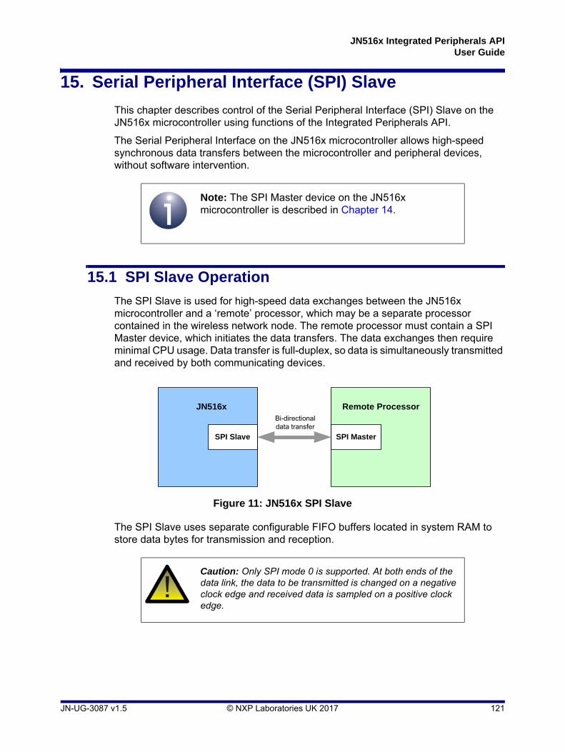
JN516x Integrated Peripherals APIUser Guide
15. Serial Peripheral Interface (SPI) Slave
This chapter describes control of the Serial Peripheral Interface (SPI) Slave on the JN516x microcontroller using functions of the Integrated Peripherals API.
The Serial Peripheral Interface on the JN516x microcontroller allows high-speed synchronous data transfers between the microcontroller and peripheral devices, without software intervention.
15.1 SPI Slave Operation
The SPI Slave is used for high-speed data exchanges between the JN516x microcontroller and a ‘remote’ processor, which may be a separate processor contained in the wireless network node. The remote processor must contain a SPI Master device, which initiates the data transfers. The data exchanges then require minimal CPU usage. Data transfer is full-duplex, so data is simultaneously transmitted and received by both communicating devices.
The SPI Slave uses separate configurable FIFO buffers located in system RAM to store data bytes for transmission and reception.
Note: The SPI Master device on the JN516x microcontroller is described in Chapter 14.
Figure 11: JN516x SPI Slave
Caution: Only SPI mode 0 is supported. At both ends of the data link, the data to be transmitted is changed on a negative clock edge and received data is sampled on a positive clock edge.
JN516x
SPI Slave
Remote Processor
SPI Master
Bi-directional data transfer
JN-UG-3087 v1.5 © NXP Laboratories UK 2017 121

Chapter 15Serial Peripheral Interface (SPI) Slave
15.1.1 SPI Bus Lines and DIO Usage
The SPI Slave uses the following bus lines:
Slave Clock Input, SPISCLK
Slave Data Output, SPISMISO
Slave Data Input, SPISMOSI
Slave-select Input, SPISSEL
These signals use the following DIO pins:
SPISCLK uses DIO15
SPISMOSI and SPISMISO use DIO12-13 or alternatively DIO16-17
SPISSEL uses DIO14
The DIO pins used for SPISMOSI and SPISMISO are configured when calling bAHI_SpiSlaveEnable().
15.1.2 SPI Slave FIFOs and Interrupts
The Data In (Receive) and Data Out (Transmit) paths of the SPI Slave device contain FIFO buffers which are located in RAM. The exact locations and sizes of these buffers are defined by the application when the SPI Slave is initialised using the function bAHI_SpiSlaveEnable(). Each buffer can be up to 255 bytes in size.
Fill-level thresholds (in bytes) must also be specified that are used to prompt the application to write data to the Transmit buffer and read data from the Receive buffer.
For the Transmit FIFO, this threshold is the fill-level which is considered low enough for more data to be written into the buffer - if interrupts are enabled, an interrupt will be generated when the amount of data in the buffer falls below this level
For the Receive FIFO, this threshold is the fill-level which is considered high enough for data to be read from the buffer - if interrupts are enabled, an interrupt will be generated when the amount of data in the buffer rises above this level
A Receive timeout duration (in microseconds) must also be specified in the above function call. Following the end of a SPI transfer, if the Receive FIFO remains not empty for this duration then a timeout interrupt will be generated (if enabled) to prompt the application to read data from the buffer. This prevents received data from remaining in the buffer for too long without being read.
SPI Slave interrupts must be enabled in order to use the buffer thresholds and Receive timeout described above. Again, interrupts can be enabled when the device is configured using bAHI_SpiSlaveEnable(). If they are enabled, a user-defined callback function to handle SPI Slave interrupts must be registered using the function vAHI_SpiSlaveRegisterCallback(). The callback function is automatically invoked when an interrupt of the type E_AHI_DEVICE_SPIS occurs. For details of the callback function prototype, refer to Appendix A.1.
122 © NXP Laboratories UK 2017 JN-UG-3087 v1.5

JN516x Integrated Peripherals APIUser Guide
15.2 Using the SPI Slave
A data transfer is conducted via the SPI Slave as follows (this procedure assumes that SPI Slave interrupts will be enabled):
1. The SPI Slave must first be initialised and configured using the function bAHI_SpiSlaveEnable(). This function allows the following to be configured:
Bit-order for transmission/reception of SPI data (LSB first or MSB first)
DIO pins used for SPISMISO and SPISMOSI
Transmit FIFO buffer, including start address in RAM, size (in bytes) and write threshold (in bytes) - see Section 15.1.2
Receive FIFO buffer, including start address in RAM, size (in bytes), read threshold (in bytes) and timeout (in microseconds) - see Section 15.1.2
SPI Slave interrupts (which should be enabled)
2. A user-defined callback function to handle SPI Slave interrupts must now be registered using vAHI_SpiSlaveRegisterCallback().
3. The application can now load transmission data into the Transmit FIFO (data will be transmitted when a transfer is initiated by the remote SPI Master):
a) The initial data must be written to the Transmit FIFO using the function vAHI_SpiSlaveTxWriteByte(). The number of bytes written must not exceed the size of the buffer. By default, if the Transmit FIFO is empty and a transfer is initiated by the remote SPI Master, the SPI Slave will transmit the data byte 0x00.
b) Subsequently, the application must wait for a write threshold interrupt to prompt further writes to the Transmit FIFO. When this interrupt occurs, the user-defined callback function will be invoked to handle the interrupt and vAHI_SpiSlaveTxWriteByte() should be called within this callback function. The number of bytes written should not exceed the size of the buffer minus the write threshold for the buffer.
4. The application can now also read any received data from the Receive FIFO. To do this, it should wait for a read threshold interrupt or a read timeout interrupt. When one of these interrupts occurs, the user-defined callback function will be invoked to handle the interrupt and the function u8AHI_SpiSlaveRxReadByte() should be called within this callback function.
Caution: The registered callback function is only preserved during sleep modes in which RAM remains powered. If RAM is powered off during sleep and interrupts are required, the callback function must be re-registered before calling u32AHI_Init() on waking.
JN-UG-3087 v1.5 © NXP Laboratories UK 2017 123

Chapter 15Serial Peripheral Interface (SPI) Slave
The functions u8AHI_SpiSlaveTxFillLevel(), u8AHI_SpiSlaveRxFillLevel() and u8AHI_SpiSlaveStatus() are provided to enable an application to monitor the SPI Slave in a non-interrupt driven manner.
Tip: Although the data transfer is full-duplex, a simplex transfer can be achieved by transferring dummy data in the unwanted direction.
124 © NXP Laboratories UK 2017 JN-UG-3087 v1.5

JN516x Integrated Peripherals APIUser Guide
16. Flash Memory
This chapter describes control of Flash memory using functions of the Integrated Peripherals API.
The JN516x microcontroller has on-chip Flash memory. This non-volatile memory is used to store the binary application and associated application data. The JN516x device can also be optionally connected to an external Flash memory device.
The Integrated Peripherals API includes functions that allow the application to erase, programme and read a sector of Flash memory. Normally, these functions are used to store and retrieve application data - this might include data to be preserved in non-volatile memory before going to sleep without RAM held.
16.1 Flash Memory Organisation and Types
Flash memory is partitioned into sectors. The number of sectors depends on the Flash device type, but the application binary is normally stored from the start of the first sector, denoted Sector 0, and the application data is stored in the final sector. A Flash memory sector which is blank (no data) comprises entirely of binary 1s. When data is written to the sector, the relevant bits are changed from 1 to 0.
The following tables provide details of the on-chip Flash memory and supported external Flash devices for the JN516x family of microcontrollers.
JN516x ChipNumber of
SectorsSector Size
(Kbytes)Total Size(Kbytes)
JN5169 16 32 512
JN5168 8 32 256
JN5164 5 32 160
JN5161 2 32 64
Table 5: On-chip Flash Memory
Manufacturer Flash DeviceNumber of
SectorsSector Size
(Kbytes)Total Size(Kbytes)
Atmel AT25F512 2 32 64
STMicroelectronics M25P05A 2 32 64
Microchip SST25VF010A 4 32 128
STMicroelectronics M25P10A 4 32 128
STMicroelectronics M25P20 4 64 256
Winbond W25X20B 4 64 256
STMicroelectronics M25P40 8 64 512
Table 6: Supported External Flash Devices
JN-UG-3087 v1.5 © NXP Laboratories UK 2017 125

Chapter 16Flash Memory
16.2 API Functions
The supplied Flash Memory functions can be used to interact with the on-chip Flash device and any compatible external Flash device (detailed in Section 16.1). The functions are able to access any sector of Flash memory - the application is stored from the first sector (0) and application data is normally stored in the final sector - you should refer to the data sheet for the Flash device to obtain the necessary sector details. The Flash Memory functions are fully detailed in Chapter 32.
16.3 Operating on Flash Memory
This section describes how to use the Flash Memory functions to erase, read from and write to a sector of Flash memory.
The first Flash memory function called must be the initialisation function bAHI_FlashInit(). In the case of external Flash memory, this function requires the attached Flash device type to be specified.
Note 1: If you wish to use both internal (on-chip) and external Flash memory devices, you will need to call bAHI_FlashInit() when switching between them.
Note 2: All Flash addresses specified in the Flash Memory functions are offsets from the start of Flash memory and not absolute addresses.
Note 3: The bAHI_FlashEECerrorInterruptSet() function can be used to enable interrupts that are generated when an error occurs in the on-chip Flash device. A user-defined callback function is also registered which is invoked when a Flash memory interrupt occurs.
Note 4: If you are not using one of the supported external Flash memory devices (see Table 6 on page 125), you will need to supply a set of custom Flash functions that will be used by the supplied Flash functions to access your Flash memory device. These custom functions must be registered in the call to bAHI_FlashInit() - for more information, refer to the description of this function in Chapter 32.
126 © NXP Laboratories UK 2017 JN-UG-3087 v1.5
JN516x Integrated Peripherals APIUser Guide
16.3.1 Erasing Data from Flash Memory
Erasing a portion of Flash memory involves setting any 0 bits to 1. The function bAHI_FlashEraseSector() can be used to erase an entire sector of Flash memory. Any sector can be erased.
16.3.2 Reading Data from Flash Memory
The function bAHI_FullFlashRead() can be used to read data from any sector of Flash memory. This function can be used to read a portion of data starting at any point within the sector.
16.3.3 Writing Data to Flash Memory
Before writing the first data to a sector of Flash memory, the sector must be blank (consisting entirely of binary 1s), as the write operation will only change 1s to 0s (where relevant). Therefore, it may be necessary to erase the relevant sector, as described in Section 16.3.1, before writing the first data to it.
The function bAHI_FullFlashProgram() can be used to write data to any sector of Flash memory. This function can be used to write a portion of data containing a multiple of 16 bytes starting on a 16-byte boundary within the sector. When adding data to existing data in a sector, you must be sure that the relevant portion of the sector is already blank (comprising all binary 1s).
One way to ensure that data is added successfully to a sector is as follows:
1. Read the entire sector into RAM (see Section 16.3.2).
2. Erase the entire sector in Flash memory (see Section 16.3.1).
3. Add the new data to the existing data in RAM.
4. Write all of this data back to the sector in Flash memory.
Caution: Be careful not to erase essential data such as the application code. The application is stored from the start of the on-chip Flash memory (starting in Sector 0).
Note: The internal Flash memory of the JN516x device has a sector-erase time of approximately 100ms.
JN-UG-3087 v1.5 © NXP Laboratories UK 2017 127
Chapter 16Flash Memory
16.4 Controlling Power to External Flash Memory
Any external Flash memory can be optionally powered off while the JN516x microcontroller is in a sleep mode (including Deep Sleep). An unpowered Flash device during sleep allows greater power savings and extends battery life.
Two functions (see below) are provided for controlling power to an external Flash device, but these are only applicable to the following STMicroelectronics devices:
STM25P05A
STM25P10A
STM25P20
STM25P40
Calling these functions for other Flash devices will have no effect.
The necessary function calls before and after sleep are outlined as follows.
Caution 1: Each sector of the internal Flash memory in the JN516x device is divided into 16-byte pagewords. A write to a non-blank pageword must not be performed - the sector containing the non-blank pageword should first be erased using bAHI_FlashEraseSector() before writing to the pageword. If the user omits the sector-erase operation, a subsequent error will likely result when reading from the pageword - this read-error will trigger an interrupt and execute the callback function registered using bAHI_FlashEECerrorInterruptSet().
Caution 2: The internal Flash memory of the JN516x device has an endurance limit of 10000 write/erase cycles per sector. Refer to the device-specific data sheet for the endurance limit of the external Flash memory.
Note: The internal Flash memory of the JN516x device has a sector write-time of approximately 1ms.
Caution: These functions must not be called when using JN516x on-chip Flash memory device (selected in bAHI_FlashInit()). Note that when using the JenOS Persistent Data Manager (PDM), the on-chip Flash memory device is automatically selected by default.
128 © NXP Laboratories UK 2017 JN-UG-3087 v1.5
JN516x Integrated Peripherals APIUser Guide
Before Sleep
The above external Flash memory devices can be powered down before entering sleep mode by calling the function vAHI_FlashPowerDown(). This function must be called before vAHI_Sleep() is called.
After Sleep
If a Flash memory device was powered down using vAHI_FlashPowerDown() before entering sleep, on waking from sleep the function vAHI_FlashPowerUp() must be called to power on the Flash memory device again.
Tip: In order to conserve power, you may wish to power down the external Flash memory device at JN516x start-up and only power up the Flash device when required.
JN-UG-3087 v1.5 © NXP Laboratories UK 2017 129

Chapter 16Flash Memory
130 © NXP Laboratories UK 2017 JN-UG-3087 v1.5

JN516x Integrated Peripherals APIUser Guide
17. EEPROM
This chapter describes access to the JN516x on-chip EEPROM using functions of the Integrated Peripherals API. This non-volatile memory is used to store data that must be preserved while the JN516x device is not powered or during sleep without RAM held. EEPROM which is blank (no data) comprises entirely of binary 0s. When data is written to it, the relevant bits are changed from 0 to 1. Functions are provided for writing to, reading from and erasing the EEPROM.
Although the functions referenced in this chapter provide direct access to the EEPROM device, it is recommended that they are not used or are used with caution, for the following reasons:
JenNet-IP and ZigBee nodes use the JenOS Persistent Data Manager (PDM) which also accesses the EEPROM. PDM is supplied in the NXP JenNet-IP and ZigBee SDKs, and is described in the JenOS User Guide (JN-UG-3075). The advantages of using PDM include:
‘Wear levelling’ to achieve the uniform use of the EEPROM
Record IDs to avoid the use of memory addresses
If PDM and the EEPROM direct-access function set are both to be used, it is important to avoid conflicts between the two - therefore, they must never access the same part of the EEPROM.
ZigBee RF4CE uses the EEPROM direct-access functions itself so, again, conflicts must be avoided.
JN-UG-3087 v1.5 © NXP Laboratories UK 2017 131

Chapter 17EEPROM
17.1 Initialisation
In order to access the EEPROM from the application, the initialisation function u16AHI_InitialiseEEP() must first be called.
The EEPROM is organised in terms of segments of 64 bytes each, and the above function returns the following information about the available segments:
Number of segments
Number of bytes in each segment
The segments are indexed from 0.
17.2 Writing to the EEPROM
A block of data can be written to a specified EEPROM segment using the function iAHI_WriteDataIntoEEPROMsegment(). The data can be written starting at any (byte) offset from the beginning of the segment. The function will not allow a segment to overflow - if the length of the data block to be written is greater than the memory space up to the end of the segment, the function will return an error and will not write any data.
17.3 Reading from the EEPROM
A block of data can be read from a specified EEPROM segment using the function iAHI_ReadDataFromEEPROMsegment(). The data can be read starting at any (byte) offset from the beginning of the segment. If the length of the data block to be read is greater than the memory space up to the end of the segment, the function will return an error and will not read any data.
17.4 Erasing the EEPROM
The EEPROM can be erased a whole segment at a time. The function iAHI_EraseEEPROMsegment() can be used to erase a specified segment.
Note: The final segment of EEPROM is reserved for production data and cannot be written to or erased.
132 © NXP Laboratories UK 2017 JN-UG-3087 v1.5

JN516x Integrated Peripherals APIUser Guide
Part II: Reference Information
JN-UG-3087 v1.5 © NXP Laboratories UK 2017 133

134 © NXP Laboratories UK 2017 JN-UG-3087 v1.5

JN516x Integrated Peripherals APIUser Guide
18. General Functions
This chapter describes various functions of the Integrated Peripherals API that are not associated with any of the main peripheral blocks on a JN516x microcontroller.
The functions in this chapter include:
API initialisation function
Functions to implement antenna diversity
Functions to control the random number generator
Processor stack overflow function
Functions for accessing on-chip Non-Volatile Memory
Functions for preserving debug information during sleep
Function for reducing the maximum receive power on JN5169
Note that the random number generator can produce interrupts which are treated as System Controller interrupts. For information on interrupt handling, see Appendix A.
Note: For guidance on using these functions in JN516x application code, refer to Chapter 2.
JN-UG-3087 v1.5 © NXP Laboratories UK 2017 135

Chapter 18General Functions
The functions are listed below, along with their page references:
Function Page
u32AHI_Init 137
vAHI_HighPowerModuleEnable 138
vAHI_AntennaDiversityOutputEnable 139
vAHI_AntennaDiversitySetPinLocation (JN5169 Only) 140
vAHI_AntennaDiversityEnable 141
u8AHI_AntennaDiversityStatus 142
vAHI_AntennaDiversityControl 143
vAHI_AntennaDiversitySwitch 144
vAHI_StartRandomNumberGenerator 145
vAHI_StopRandomNumberGenerator 146
u16AHI_ReadRandomNumber 147
bAHI_RndNumPoll 148
vAHI_SetStackOverflow 149
vAHI_WriteNVData 151
u32AHI_ReadNVData 152
vAHI_InterruptSetPriority 153
vAHI_StoreDebug 154
vAHI_RestoreDebug 155
vAHI_RadioSetReducedInputPower (JN5169 Only) 156
136 © NXP Laboratories UK 2017 JN-UG-3087 v1.5
JN516x Integrated Peripherals APIUser Guide
u32AHI_Init
Description
This function initialises the Integrated Peripherals API. It should be called after every reset and wake-up, and before any other Integrated Peripherals API functions are called.
Parameters
None
Returns
0 if initialisation failed, otherwise a 32-bit version number for the API (most significant 16 bits are main revision, least significant 16 bits are minor revision).
uint32 u32AHI_Init(void);
Caution: If you are using JenOS (Jennic Operating System), you must not call this function explicitly in your code, as the function is called internally by JenOS. This applies principally to users who are developing ZigBee PRO applications.
Note: This function must be called before initialising the Application Queue API (if used). For more information on the latter, refer to the IEEE 802.15.4 Stack User Guide (JN-UG-3024).
JN-UG-3087 v1.5 © NXP Laboratories UK 2017 137

Chapter 18General Functions
vAHI_HighPowerModuleEnable
Description
This function allows control for transmission and reception on a JN516x high-power module to be enabled or disabled. Control for transmission and reception must both be enabled or disabled at the same time (enabling only one of them is not supported). The function should be called before using the radio transceiver on a JN516x high-power module.
Parameters
bRFTXEn Enable/disable control for high-power module transmission (must be same setting as for bRFRXEn):TRUE - enable control for high-power module transmissionFALSE - disable control for high-power module transmission
bRFRXEn Enable/disable control for high-power module reception(must be same setting as for bRFTXEn):TRUE - enable control for high-power module receptionFALSE - disable control for high-power module reception
Returns
None
void vAHI_HighPowerModuleEnable(bool_t bRFTXEn, bool_t bRFRXEn);
Note 1: This function should only be used with a JN516x high-power module manufactured by NXP.
Note 2: Instead of using this function to enable/disable a high-power module, you are advised to use the function vAppApiSetHighPowerMode() from the NXP 802.15.4 Stack API (supplied in the file AppApi.h in all the JN516x SDKs).
Caution: This function must not be used to enable a JN516x high-power module which will operate in channel 26 of the 2.4GHz band, since emission regulations will be breached. The function vAppApiSetHighPowerMode() should be used instead (see Note 2 above), which enables a mechanism to reduce the output power on channel 26 so that the emission regulations are met.
138 © NXP Laboratories UK 2017 JN-UG-3087 v1.5
JN516x Integrated Peripherals APIUser Guide
vAHI_AntennaDiversityOutputEnable
Description
This function can be used to individually enable or disable the use of two DIOs for the control of antenna diversity. These DIOs are, by default, DIO12 and DIO13. However, on the JN5169 device, DIO0 and DIO1 can respectively be used instead - if required, the function vAHI_AntennaDiversitySetPinLocation() must first be called to select this alternative configuration.
The use of antenna diversity requires two antennas to be connected to the JN516x device via a switch controlled by the pair of DIOs.
Parameters
bOddOutEn Enable/disable setting for DIO12 (or DIO0 on JN5169):TRUE - enable antenna diversity control output on pinFALSE - disable antenna diversity control output on pin
bEvenOutEn Enable/disable setting for DIO13 (or DIO1 on JN5169):TRUE - enable antenna diversity control output on pinFALSE - disable antenna diversity control output on pin
Returns
None
void vAHI_AntennaDiversityOutputEnable(bool_t bOddOutEn,bool_t bEvenOutEn);
JN-UG-3087 v1.5 © NXP Laboratories UK 2017 139

Chapter 18General Functions
vAHI_AntennaDiversitySetPinLocation (JN5169 Only)
Description
This function can be used on the JN5169 device to change the DIO pins assigned to the antenna diversity control outputs. By default, these outputs use DIO12 and DIO13, but this function can be used to moved these outputs to DIO0 and DIO1 respectively.
Parameters
bLocationDIO0_1 Boolean indicating the pair of pins to be assigned to antenna diversity control outputs:TRUE - DIO0 and DIO1FALSE - DIO12 and DIO13
Returns
None
void vAHI_AntennaDiversitySetPinLocation(bool_t bLocationDIO0_1);
140 © NXP Laboratories UK 2017 JN-UG-3087 v1.5

JN516x Integrated Peripherals APIUser Guide
vAHI_AntennaDiversityEnable
Description
This function can be used to independently enable/disable antenna diversity on the transmit and receive paths. The use of antenna diversity requires two antennas to be connected to the JN516x device via a switch controlled by two DIO pins - these pins are enabled for antenna diversity use by calling the function vAHI_AntennaDiversityOutputEnable().
Parameters
bRxDiversity Enable/disable antenna diversity on receive path:TRUE - enable FALSE - disable
bTxDiversity Enable/disable antenna diversity on transmit path:TRUE - enable FALSE - disable
Returns
None
void vAHI_AntennaDiversityEnable(bool_t bRxDiversity,bool_t bTxDiversity);
JN-UG-3087 v1.5 © NXP Laboratories UK 2017 141

Chapter 18General Functions
u8AHI_AntennaDiversityStatus
Description
This function can be used to obtain the latest antenna diversity status (when two antennae are connected to the JN516x device and antenna diversity has been enabled through a call to vAHI_AntennaDiversityEnable()). The use of antenna diversity requires two antennas to be connected to the JN516x device via a switch controlled by two DIO pins - these pins are enabled for antenna diversity use by calling the function vAHI_AntennaDiversityOutputEnable().
The function returns a bitmap containing the following information:
Antenna used for the last transmit (bit 0)
Antenna used for the last receive (bit 1)
Currently selected antenna (bit 2)
A bit is set to 0 or 1 according to the antenna used where the value corresponds to the state of the antenna control signal output on one DIO pin (DIO12 or DIO0) - the state of the antenna control signal output on the other DIO pin (DIO13 or DIO1) will be the complement of this value.
Parameters
None
Returns
Result is a bitmap which can be bitwise ANDed with the following masks:
E_AHI_ANTDIV_STAT_TX_MASK (0x1) - extracts antenna used for last Tx
E_AHI_ANTDIV_STAT_RX_MASK (0x2) - extracts antenna used for last Rx
E_AHI_ANTDIV_STAT_ANT_MASK (0x4) - extracts antenna currently selected
uint8 u8AHI_AntennaDiversityStatus(void);
142 © NXP Laboratories UK 2017 JN-UG-3087 v1.5

JN516x Integrated Peripherals APIUser Guide
vAHI_AntennaDiversityControl
Description
This function can be used for application control of antenna diversity (enabled through a call to vAHI_AntennaDiversityEnable()), in the following ways:
Receive diversity RSSI threshold can be set which determines the minimum acceptable receive signal strength below which the antenna may be switched (also subject to other conditions - see Section 2.3)
Receive diversity Correlation threshold can be set which determines the minimum acceptable receive signal quality below which the antenna may be switched (also subject to other conditions - see Section 2.3)
Parameters
u8RxRssiThreshold Receive diversity RSSI threshold, in 1dB steps from 0 to 31 (default value is 25 - it not recommended to use values less than 25)
u8RxCorrThreshold Receive diversity Correlation threshold, from 0 to 63 (default value is 25 - it is not recommended to use values less than 25 or greater than 40)
Returns
None
void vAHI_AntennaDiversityControl(uint8 u8RxRssiThreshold,uint8 u8RxCorrThreshold);
JN-UG-3087 v1.5 © NXP Laboratories UK 2017 143

Chapter 18General Functions
vAHI_AntennaDiversitySwitch
Description
This function can be used by an application to manually switch the currently selected antenna for the control of antenna diversity. Note that calling this function will generally not be required because it is expected that most applications will make use of the automatic transmit and/or receive antenna diversity control features that are enabled by calling vAHI_AntennaDiversityEnable().
The use of antenna diversity requires two antennas to be connected to the JN516x device via a switch controlled by two DIO pins - these pins are enabled for antenna diversity use by calling the function vAHI_AntennaDiversityOutputEnable().
Parameters
None
Returns
None
void vAHI_AntennaDiversitySwitch(void);
144 © NXP Laboratories UK 2017 JN-UG-3087 v1.5

JN516x Integrated Peripherals APIUser Guide
vAHI_StartRandomNumberGenerator
Description
This function starts the random number generator on the JN516x device, which produces 16-bit random values. The generator can be started in one of two modes:
Single-shot mode: Stop generator after one random number
Continuous mode: Run generator continuously - this will generate a random number every 256µs
A randomly generated value can subsequently be read using the function u16AHI_ReadRandomNumber(). The availability of a new random number, and therefore the need to call the ‘read’ function, can be determined using either interrupts or polling:
When random number generator interrupts are enabled, an interrupt will occur each time a new random value is generated. These interrupts are handled by the callback function registered with vAHI_SysCtrlRegisterCallback() - also refer to Appendix A.
Alternatively, when random number generator interrupts are disabled, the function bAHI_RndNumPoll() can be used to poll for the availability of a new random value.
When running continuously, the random number generator can be stopped using the function vAHI_StopRandomNumberGenerator().
Note that the random number generator uses the 32kHz clock domain (see Section 3.1) and will not operate properly if a high-precision external 32kHz clock source is used. Therefore, if generating random numbers in your application, you are advised to use the internal RC oscillator or a low-precision external clock source.
Parameters
bMode Generator mode:E_AHI_RND_SINGLE_SHOT (single-shot mode)E_AHI_RND_CONTINUOUS (continuous mode)
bIntEn Enable/disable interrupts setting:E_AHI_INTS_ENABLED(enable)E_AHI_INTS_DISABLED(disable)
Returns
None
void vAHI_StartRandomNumberGenerator(bool_t const bMode, bool_t const bIntEn);
JN-UG-3087 v1.5 © NXP Laboratories UK 2017 145

Chapter 18General Functions
vAHI_StopRandomNumberGenerator
Description
This function stops the random number generator on the JN516x device, if it has been started in continuous mode using vAHI_StartRandomNumberGenerator().
Parameters
None
Returns
None
void vAHI_StopRandomNumberGenerator(void);
146 © NXP Laboratories UK 2017 JN-UG-3087 v1.5

JN516x Integrated Peripherals APIUser Guide
u16AHI_ReadRandomNumber
Description
This function obtains the last 16-bit random value produced by the random number generator on the JN516x device. The function can only be called once the random number generator has generated a new random number.
The availability of a new random number, and therefore the need to call u16AHI_ReadRandomNumber(), is determined using either interrupts or polling:
When random number generator interrupts are enabled, an interrupt will occur each time a new random value is generated.
Alternatively, when random number generator interrupts are disabled, the function bAHI_RndNumPoll() can be used to poll for the availability of a new random value.
Interrupts are enabled or disabled when the random number generator is started using vAHI_StartRandomNumberGenerator().
Parameters
None
Returns
16-bit random integer
uint16 u16AHI_ReadRandomNumber(void);
JN-UG-3087 v1.5 © NXP Laboratories UK 2017 147
Chapter 18General Functions
bAHI_RndNumPoll
Description
This function can be used to poll the random number generator on the JN516x device - that is, to determine whether the generator has produced a new random value.
Note that this function does not obtain the random value, if one is available - the function u16AHI_ReadRandomNumber() must be called to read the value.
Parameters
None
Returns
Availability of new random value, one of:TRUE - random value availableFALSE - no random value available
bool_t bAHI_RndNumPoll(void);
148 © NXP Laboratories UK 2017 JN-UG-3087 v1.5

JN516x Integrated Peripherals APIUser Guide
vAHI_SetStackOverflow
Description
This function allows processor stack overflow detection to be enabled/disabled on the JN516x device and a threshold to be set for the generation of a stack overflow exception.
The JN516x processor has a stack for temporary storage of data during code execution, such as local variables and return addresses from functions. The base address of RAM is 0x04000000 for the JN516x. The stack begins at the highest location in RAM (e.g. 0x04008000 for the JN5168) and grows downwards through RAM, as required. Thus, the stack size is dynamic, typically growing when a function is called and shrinking when returning from a function. It is difficult to determine by code inspection exactly how large the stack may grow. The lowest memory location currently used by the stack is stored in the stack pointer.
Applications occupy the bottom region of RAM and the memory space required by the applications is fixed at build time. Above the applications is the heap, which is used to store data. The heap grows upwards through RAM as data is added. Since the actual space needed by the processor stack is not known at build time, it is possible for the processor stack to grow downwards into the heap space while the application is running. This condition is called a stack overflow and results in the processor stack corrupting the heap (and potentially the application).
This function allows a threshold RAM address to be set, such that a stack overflow exception is generated if and when the stack pointer falls below this threshold address. The threshold address is specified as a 17-bit offset from the base of RAM (i.e. from 0x04000000). For example, the threshold address offset for the JN5168 can take a value up to 0x07FFC, so a good starting point is 0x07800. Note, the stack pointer is word-aligned, so the bottom 2 bits of the address are always 0.
The stack overflow exception handler function should first be developed before enabling stack overflow detection.
void vAHI_SetStackOverflow(bool_t bStkOvfEn, uint32 u32Addr);
Note 1: If a stack overflow is detected, the detection mechanism is automatically disabled and this function must be called to re-enable it.
Note 2: The stack overflow exception handler function should have the following prototype definition:
PUBLIC void vException_StackOverflow(void);
We would not expect an exception handler written in C to return - once it has performed any actions, it should either sit in a loop or reset the device.
JN-UG-3087 v1.5 © NXP Laboratories UK 2017 149

Chapter 18General Functions
Parameters
bStkOvfEn Enable/disable stack overflow detection:TRUE - enable detectionFALSE - disable detection (default)
u32Addr 17-bit stack overflow threshold
Returns
None
150 © NXP Laboratories UK 2017 JN-UG-3087 v1.5

JN516x Integrated Peripherals APIUser Guide
vAHI_WriteNVData
Description
This function writes the specified 32-bit word to the specified location in the JN516x internal 4-word NVM (Non-Volatile Memory). The JN516x internal NVM contains four 32-bit locations, numbered 0 to 3.
Parameters
u8Location Number of NVM location to which word is to be written: 0, 1, 2 or 3
u32WriteData 32-bit word to be written to NVM
Returns
None
void vAHI_WriteNVData(uint8 u8Location, uint32 u32WriteData);
JN-UG-3087 v1.5 © NXP Laboratories UK 2017 151
Chapter 18General Functions
u32AHI_ReadNVData
Description
This function reads the 32-bit word from the specified location in the JN516x internal 4-word NVM (Non-Volatile Memory). The JN516x internal NVM contains four 32-bit locations, numbered 0 to 3.
Parameters
u8Location Number of NVM location from which word is to be read: 0, 1, 2 or 3
Returns
32-bit word read from NVM
uint32 u32AHI_ReadNVData(uint8 u8Location);
152 © NXP Laboratories UK 2017 JN-UG-3087 v1.5

JN516x Integrated Peripherals APIUser Guide
vAHI_InterruptSetPriority
Description
This function can be used to configure a set of interrupt sources to have the specified interrupt priority level.
The priority level is set in the range 0 to 15, where 0 represents interrupts disabled and 15 is the highest interrupt priority level (the default priority level is 8). The interrupt sources to which this priority level will be applied are specified in a bitmap - each bit of the bitmap represents an interrupt source and should be set to ‘1’ to include this interrupt. To help construct this bitmap, enumerations of the form MICRO_ISR_MASK_xxx are supplied in the file MicroSpecific.h.
The function can be called multiple times to set different priorities for different interrupt sources.
Parameters
u16Mask Bitmap specifying the interrupt sources to which the priority level will be applied
u8Level Interrupt priority level (in the range 0 to 15)
Returns
None
void vAHI_InterruptSetPriority(uint16 u16Mask, uint8 u8Level);
JN-UG-3087 v1.5 © NXP Laboratories UK 2017 153
Chapter 18General Functions
vAHI_StoreDebug
Description
This function can be used to store the contents of the Debug registers in an array in RAM so that they will be preserved during sleep with memory held (and debug information will not be lost).
A pointer to a uint32 array must be provided to which the register contents will saved. This array will contain one element per register and so the number of elements must be equal to the number of registers. This number is defined by the macro AHI_STORE_DEBUG_REGISTER_COUNT in the AppHardwareApi.h file. The array should be dimensioned using this macro - for example:
uint32 au32DebugRegisterStorage[AHI_STORE_DEBUG_REGISTER_COUNT];
On waking from sleep, the function vAHI_RestoreDebug() should be called to restore the saved debug information from the array to the Debug registers.
Parameters
pRegStorage Pointer to an array to receive the contents of the Debug registers (with one array element per register).
Returns
None
void vAHI_StoreDebug(uint32 *pRegStorage);
154 © NXP Laboratories UK 2017 JN-UG-3087 v1.5

JN516x Integrated Peripherals APIUser Guide
vAHI_RestoreDebug
Description
This function can be used to restore preserved debug data from RAM to the Debug registers following sleep with memory held. Thus, this function should be called on waking from sleep if the function vAHI_StoreDebug() was called before entering sleep.
Parameters
pRegStorage Pointer to the array in which preserved debug data is stored
Returns
None
void vAHI_RestoreDebug(uint32 *pRegStorage);
JN-UG-3087 v1.5 © NXP Laboratories UK 2017 155

Chapter 18General Functions
vAHI_RadioSetReducedInputPower (JN5169 Only)
Description
This function can be used to reduce the maximum radio signal power that the JN5169 device can receive before saturating. The function can be called at any time.
The JN5169 device can receive radio signals of up to 10 dBm before the input is saturated. However, this function can be used to configure the device to saturate at a lower incoming signal level of 0 dBm, which has the advantage of drawing less current and prolonging battery life.
The function has a Boolean parameter for which TRUE selects the reduced maximum input level and FALSE selects the normal (default) input level.
Parameters
bReduced Enable/disable reduced maximum input power:TRUE - Enable reduced saturation levelFALSE - Disable reduced saturation level (restore default level)
Returns
None
void vAHI_RadioSetReducedInputPower(bool_t bReduced);
156 © NXP Laboratories UK 2017 JN-UG-3087 v1.5

JN516x Integrated Peripherals APIUser Guide
19. System Controller Functions
This chapter describes the functions that interface to the System Controller on the JN516x microcontroller.
The functions detailed in this chapter cover the following areas:
Power management
Clock management
Supply voltage monitoring (Voltage brownout)
Chip reset
The System Controller functions are listed below, along with their page references:
Function Page
u16AHI_PowerStatus 159
vAHI_CpuDoze 160
vAHI_Sleep 161
vAHI_ProtocolPower 163
bAHI_Set32KhzClockMode 164
vAHI_Init32KhzXtal 165
vAHI_Trim32KhzRC 166
vAHI_SelectClockSource 167
bAHI_GetClkSource 168
bAHI_SetClockRate 169
u8AHI_GetSystemClkRate 170
bAHI_Clock32MHzStable 172
vAHI_ClockXtalPull 173
vAHI_EnableFastStartUp 174
bAHI_TrimHighSpeedRCOsc 175
vAHI_OptimiseWaitStates 176
vAHI_BrownOutConfigure 177
bAHI_BrownOutStatus 179
bAHI_BrownOutEventResetStatus 180
u32AHI_BrownOutPoll 181
vAHI_SwReset 182
vAHI_SetJTAGdebugger 183
vAHI_ClearSystemEventStatus 184
Note: For information on the above chip features and guidance on using the System Controller functions in JN516x application code, refer to Chapter 3.
JN-UG-3087 v1.5 © NXP Laboratories UK 2017 157

Chapter 19System Controller Functions
vAHI_SysCtrlRegisterCallback 185
158 © NXP Laboratories UK 2017 JN-UG-3087 v1.5

JN516x Integrated Peripherals APIUser Guide
u16AHI_PowerStatus
Description
This function returns power domain status information for the JN516x microcontroller - in particular, whether:
Device has completed a sleep-wake cycle
RAM contents were retained during sleep
Analogue power domain is switched on
Protocol logic is operational (clock is enabled)
Watchdog timeout was responsible for the last device restart
32kHz clock is ready (e.g. following a reset or wake-up)
Device has just come out of Deep Sleep mode (rather than a reset)
Note that you must check whether the 32kHz clock is ready before starting a wake timer.
Parameters
None
Returns
Returns the power domain status information in bits 0-3, 7 and 10-11 of the 16-bit return value:
uint16 u16AHI_PowerStatus(void);
Bit Reads a ‘1’ if...
0 Device has completed a sleep-wake cycle
1 RAM contents were retained during sleep
2 Analogue power domain is switched on
3 Protocol logic is operational
4-6 Unused
7 Watchdog caused last device restart
8-9 Unused
10 32kHz clock is ready
11 Device has just come out of Deep Sleep mode
12-15 Unused
JN-UG-3087 v1.5 © NXP Laboratories UK 2017 159

Chapter 19System Controller Functions
vAHI_CpuDoze
Description
This function puts the device into Doze mode by stopping the clock to the CPU (other on-chip components are not affected by this function and so will continue to operate normally, e.g. on-chip RAM will remain powered and so retain its contents). The CPU will cease operating until an interrupt occurs to re-start normal operation. Disabling the CPU clock in this way reduces the power consumption of the device during inactive periods.
The function returns when the CPU re-starts.
Parameters
None
Returns
None
void vAHI_CpuDoze(void);
160 © NXP Laboratories UK 2017 JN-UG-3087 v1.5

JN516x Integrated Peripherals APIUser Guide
vAHI_Sleep
Description
This function puts the JN516x device into Sleep mode, being one of four ‘normal’ Sleep modes or Deep Sleep mode. The normal sleep modes are distinguished by whether on-chip RAM remains powered and whether the 32kHz oscillator is left running during sleep (see parameter description below).
In a normal sleep mode, the device can be woken by a reset or one of the following interrupts:
DIO interrupt
Wake timer interrupt (needs 32kHz oscillator to be left running during sleep)
Comparator interrupt
Pulse counter interrupt
External Flash memory is not powered down during normal sleep mode. If required, you can power down the Flash memory device using the function vAHI_FlashPowerDown(), which must be called before vAHI_Sleep(), provided you are using a compatible Flash memory device - refer to the description of vAHI_FlashPowerDown() on page 393.
In Deep Sleep mode, all components of the chip are powered down and the device can only be woken by the device’s reset line being pulled low or an external event which triggers a change on a DIO pin (the relevant DIO must be configured as an input and DIO interrupts must be enabled).
When the device restarts, it will begin processing at the cold start or warm start entry point, depending on the Sleep mode from which the device is waking (see below). This function does not return.
void vAHI_Sleep(teAHI_SleepMode sSleepMode);
Note 1: If an external source is used for the 32kHz oscillator on the JN516x device (see page 157), it is not recommended that the oscillator is stopped on entering Sleep mode.
Note 2: Registered callback functions are only preserved during Sleep modes in which RAM remains powered. If RAM is powered off during sleep and interrupts are required, any callback functions must be re-registered before calling u32AHI_Init() on waking. Alternatively, a DIO wake source can be resolved using u32AHI_DioWakeStatus().
JN-UG-3087 v1.5 © NXP Laboratories UK 2017 161

Chapter 19System Controller Functions
Parameters
sSleepMode Required Sleep mode, one of:E_AHI_SLEEP_OSCON_RAMON
32kHz oscillator on and RAM on (warm restart)E_AHI_SLEEP_OSCON_RAMOFF
32kHz oscillator on and RAM off (cold restart)E_AHI_SLEEP_OSCOFF_RAMON
32kHz oscillator off and RAM on (warm restart)E_AHI_SLEEP_OSCOFF_RAMOFF
32kHz oscillator off and RAM off (cold restart)E_AHI_SLEEP_DEEP
Deep Sleep (all components off - cold restart)
Returns
None
162 © NXP Laboratories UK 2017 JN-UG-3087 v1.5

JN516x Integrated Peripherals APIUser Guide
vAHI_ProtocolPower
Description
This function is used to enable or disable the clock to the wireless transceiver - the clock is simply disabled (gated) while the domain remains powered.
If you intend to switch the clock off and then back on again, without performing a reset or going through a sleep cycle, you must first save the current IEEE 802.15.4 MAC settings before switching off the clock. Upon switching the clock on again, the MAC settings must be restored from the saved settings. You can save and restore the MAC settings using functions of the 802.15.4 Stack API:
To save the MAC settings, use the function vAppApiSaveMacSettings().
Switching the clock back on can then be achieved by restoring the MAC settings using the function vAppApiRestoreMacSettings() (this function automatically calls vAHI_ProtocolPower() to switch on the clock)
The MAC settings save and restore functions are described in the 802.15.4 Stack API Reference Manual (JN-RM-2002).
While this clock is off, you must not make any calls into the stack, as this may result in the stack attempting to access the associated hardware (which is disabled) and therefore cause an exception.
Parameters
bOnNotOff Setting for clock to wireless transceiver:TRUE to switch the clock ONFALSE to switch the clock OFF
Returns
None
void vAHI_ProtocolPower(bool_t bOnNotOff);
Caution: Do not call vAH_ProtocolPower(FALSE) while the 802.15.4 MAC layer is active, otherwise the device may freeze.
JN-UG-3087 v1.5 © NXP Laboratories UK 2017 163
Chapter 19System Controller Functions
bAHI_Set32KhzClockMode
Description
This function selects an external source for the 32kHz clock for the JN516x device (the function is used to move from the internal source to an external source). The selected clock can be either of the following options:
External module (RC circuit): This clock must be supplied on DIO9
External crystal: This circuit must be attached on DIO9 and DIO10
If the external crystal is selected and is not already running, it will be started and this function will not return until the crystal has stabilised (which can take up to 1 second).
If this function or vAHI_Init32KhzXtal() is not called, the internal 32kHz RC oscillator is used by default. Note that once an external 32kHz clock source has been selected using this function, it is not possible to switch back to the internal RC oscillator.
If required, this function should be called near the start of the application. In particular, if selecting the external crystal, the function must be called before Timer 0 and any wake timers are used by the application, since these timers are used by the function when switching the clock source to the external crystal.
Note that there is no need to explicitly configure DIO9 or DIO10 as an input, as this is done automatically by the function.
When selecting an external module, you must disable the pull-up on DIO9 using the function vAHI_DioSetPullup(). However, when selecting the external crystal, the pull-ups on DIO9 and DIO10 are disabled automatically.
Parameters
u8Mode External 32kHz clock source:E_AHI_EXTERNAL_RC (external module)E_AHI_XTAL (external crystal)
Returns
TRUE - valid clock source specifiedFALSE - invalid clock source specified
bool_t bAHI_Set32KhzClockMode(uint8 const u8Mode);
164 © NXP Laboratories UK 2017 JN-UG-3087 v1.5

JN516x Integrated Peripherals APIUser Guide
vAHI_Init32KhzXtal
Description
This function starts an external crystal and switches the 32kHz clock source for the JN516x device to it.
The external crystal must be connected to the device via DIO9 (pin 32) and DIO10 (pin 33). There is no need to explicitly configure DIO9 or DIO10 as an input, as this is done automatically by the function.
The external crystal that has been started needs time to stabilise before it can be used as a clock source. The function returns immediately before the clock stabilises and the application can perform other processing or put the JN516x device into sleep mode while waiting for the crystal to become ready - it takes up to 1 second to stabilise. In the case of sleep, the application should typically set a wake timer to wake the device after 1 second.
If this function or bAHI_Set32KhzClockMode() is not called, the internal 32kHz RC oscillator is used by default. Note that once an external 32kHz clock source has been selected using this function, it is not possible to switch back to the internal RC oscillator.
Parameters
None
Returns
None
void vAHI_Init32KhzXtal(void);
JN-UG-3087 v1.5 © NXP Laboratories UK 2017 165
Chapter 19System Controller Functions
vAHI_Trim32KhzRC
Description
This function sets the electrical current consumption of the 32kHz RC oscillator (external module), which determines the accuracy of the clock frequency produced - the higher the current, the more accurate the generated clock frequency.
Presently, two current settings are available; 0.53µA and 0.35µA, with corresponding frequency calibration errors of ±300ppm and ±600ppm, respectively.
Parameters
u8Value Current consumption to be set:0: Reserved1: Reserved2: 0.53µA (default)3: 0.35µA4-7: No effect
Returns
None
void vAHI_Trim32KhzRC(uint8 u8Value);
166 © NXP Laboratories UK 2017 JN-UG-3087 v1.5
JN516x Integrated Peripherals APIUser Guide
vAHI_SelectClockSource
Description
This function selects the clock source for the system clock on the JN516x device. The clock options are:
Crystal oscillator (XTAL) of frequency 32MHz, derived from external crystal
Internal high-speed RC oscillator of frequency 27MHz (uncalibrated), but can be adjusted to 32MHz (calibrated) using the function bAHI_TrimHighSpeedRCOsc()
If used, the external crystal is connected to pins 4 and 5.
The CPU clock and peripheral clock are divided down versions of this clock source. The CPU clock divisor is controlled using the function bAHI_SetClockRate(). The peripheral clock is produced by dividing this clock source by two. Thus, the crystal oscillator will produce a 16MHz peripheral clock and the RC oscillator will produce a peripheral clock of 13.5MHz (±18%, uncalibrated) or 16MHz (±5% calibrated).
When the RC oscillator is selected, the function allows the crystal oscillator to be powered down, in order to save power.
If the crystal oscillator is selected using this function but the oscillator is not already running when the function is called (see vAHI_EnableFastStartUp()), typically 1ms will be required for the oscillator to become stable once it has powered up. The function will not return until the oscillator has stabilised.
Parameters
bClkSource System clock source: TRUE - RC oscillatorFALSE - crystal oscillator
bPowerDown Power down crystal oscillator: TRUE - power down when not neededFALSE - leave powered up (when not in Sleep mode)
Returns
None
void vAHI_SelectClockSource(bool_t bClkSource, bool_t bPowerDown);
Caution: You will not be able to run the full system while using the RC oscillator. It is possible to execute code while using this clock source, but it is not possible to transmit or receive. Further, timing intervals for the timers may need to be based on a frequency of 13.5MHz.
JN-UG-3087 v1.5 © NXP Laboratories UK 2017 167

Chapter 19System Controller Functions
bAHI_GetClkSource
Description
This function obtains the identity of the clock source for the system clock on the JN516x device. The clock options are:
Crystal oscillator (XTAL) of frequency 32MHz, derived from external crystal
Internal high-speed RC oscillator of frequency 27MHz (uncalibrated), but can be adjusted to 32MHz (calibrated) using the function bAHI_TrimHighSpeedRCOsc()
If the high-speed RC oscillator is the system clock source, bAHI_GetClkSource() does not indicate the operating frequency of the oscillator.
Parameters
None
Returns
Clock source, one of:TRUE - RC oscillatorFALSE - Crystal oscillator
bool_t bAHI_GetClkSource(void);
168 © NXP Laboratories UK 2017 JN-UG-3087 v1.5

JN516x Integrated Peripherals APIUser Guide
bAHI_SetClockRate
Description
This function is used to select a CPU clock rate on the JN516x device by setting the divisor used to derive the CPU clock from the system source clock.
The system clock source is selected using the function vAHI_SelectClockSource() as one of:
32MHz external crystal oscillator
High-speed internal RC oscillator of frequency 27MHz (uncalibrated), but can be adjusted to 32MHz (calibrated) using the function bAHI_TrimHighSpeedRCOsc()
The possible divisors are 1, 2, 4,8, 16 and 32.
Irrespective of the setting made with this function, the CPU clock rate will default to 16MHz or 13.5MHz (clock divisor of 2) following sleep - that is, the clock divisor configured before sleep is not automatically re-applied after sleep.
Parameters
u8Speed Divisor for desired CPU clock frequency:
Returns
TRUE - successfulFALSE - invalid divisor value specified
bool_t bAHI_SetClockRate(uint8 u8Speed);
u8Speed Clock DivisorResulting Frequency (MHz)
From 32MHz From 27MHz
000 8 4 3.38
001 4 8 6.75
010 2 16 13.5
011 1 32 27
100Invalid
101
110 32 1 0.84
111 16 2 1.69
Note: When the RC oscillator is used as the source, the resulting CPU clock frequency is dictated by the actual RC oscillator frequency, which can be 27MHz (±18%) or 32MHz (±5% when calibrated).
JN-UG-3087 v1.5 © NXP Laboratories UK 2017 169

Chapter 19System Controller Functions
u8AHI_GetSystemClkRate
Description
This function obtains the divisor used to divide down the source clock to produce the CPU clock on the JN516x device.
The system clock source is selected using the function vAHI_SelectClockSource() as one of:
32MHz external crystal oscillator
High-speed internal RC oscillator of frequency 27MHz (uncalibrated), but can be adjusted to 32MHz using the function bAHI_TrimHighSpeedRCOsc()
The current clock source can be obtained using the function bAHI_GetClkSource(), but this function does not indicate the operating frequency of the RC oscillator (if used).
The divisor for the CPU clock is configured using bAHI_SetClockRate().
The possible divisors are 1, 2, 4, 8, 16 and 32. The CPU clock frequency can be calculated by dividing the source clock frequency by the divisor returned by this function. The results are summarised in the table below.
Parameters
None
uint8 u8AHI_GetSystemClkRate(void);
Returned Value Clock DivisorResulting Frequency (MHz)
From 32MHz From 27MHz
0 8 4 3.38
1 4 8 6.75
2 2 16 13.5
3 1 32 27
4Invalid
5
6 32 1 0.84
7 16 2 1.69
Note: When the RC oscillator is used as the source, the resulting system clock frequency is dictated by the actual RC oscillator frequency, which can be 27MHz (±18%) or 32MHz (±5% when calibrated).
170 © NXP Laboratories UK 2017 JN-UG-3087 v1.5

JN516x Integrated Peripherals APIUser Guide
Returns
0: Divisor of 8
1: Divisor of 4
2: Divisor of 2
3: Divisor of 1 (source frequency untouched)
6: Divisor of 32
7: Divisor of 16
JN-UG-3087 v1.5 © NXP Laboratories UK 2017 171

Chapter 19System Controller Functions
bAHI_Clock32MHzStable
Description
This function can be used to check whether the 32MHz crystal oscillator (sourced externally) is running and stable.
Parameters
None
Returns
TRUE - oscillator is stable
FALSE - oscillator is not stable
bool_t bAHI_Clock32MHzStable(void);
172 © NXP Laboratories UK 2017 JN-UG-3087 v1.5
JN516x Integrated Peripherals APIUser Guide
vAHI_ClockXtalPull
Description
This function can be used to decrease (pull) the frequency of the 32MHz crystal oscillator by increasing the crystal load capacitance in the oscillator tuning circuit. If the JN516x device operates at temperatures in excess of 85°C, it may be necessary to call this function to maintain the frequency tolerance of the clock within the 40ppm limit specified by the IEEE 802.15.4 standard.
The crystal pulling coefficient specifies the sensitivity of the crystal frequency with respect to the crystal load capacitance. Crystals suitable for use with the JN516x will typically have a crystal pulling coefficient value in the range of 15 to 25 ppm/pF. Although the crystal pulling coefficient has a positive value, it should be noted that the crystal frequency will decrease with increasing crystal load capacitance.
The formula for calculating the crystal pulling coefficient (∆f) is given by:
where,
Cm is the crystal motional capacitance (e.g. 4.4fF)CL is the crystal load capacitance (e.g. 9pF)CS is the crystal shunt or package capacitance (e.g. 1pF)
The example crystal capacitance values quoted above yield a crystal pulling coefficient of 22ppm/pF. Therefore, an increase of the crystal load capacitance (CL) by 1pF will reduce the crystal oscillating frequency by 22ppm.
Parameters
u8PullValue Pull-value controls the additional crystal load capacitance:
0: No additional crystal load capacitance (default) 1: 1pF2: 2pF for JN5169, 1pF for other JN516x devices3: 3pF for JN5169, 2pF for other JN516x devices
Returns
None
void vAHI_ClockXtalPull(uint8 u8PullValue);
Note: Please refer to the JN516x data sheet and the crystal manufacturer data sheet for specific details of the crystal capacitances. Also refer to the Application Note JN516x Temperature-dependent Operating Guidelines (JN-AN-1186) for details of the crystal oscillator frequency compensation over temperature.
fCm 106
2 CL CS+ 2--------------------------------------= ppm F
JN-UG-3087 v1.5 © NXP Laboratories UK 2017 173

Chapter 19System Controller Functions
vAHI_EnableFastStartUp
Description
This function can be used to modify the (default) fast start-up following sleep. If required, the function must be called before entering sleep mode.
The external 32MHz crystal oscillator is powered down during sleep and takes some time to become available again when the JN516x device wakes. A more rapid start-up from sleep can be achieved by using the internal high-speed RC oscillator immediately on waking and then switching to the crystal oscillator when it becomes available. This allows initial processing at wake-up to proceed before the crystal oscillator is ready. This rapid start-up following sleep occurs automatically by default.
This function can be used to configure the switch to the crystal oscillator to be either automatic or manual (selected through the bMode parameter):
Automatic switch: The crystal oscillator starts immediately on waking from sleep (irrespective of the setting of the bPowerDown parameter - see below), allowing it to warm up and stabilise while the boot code is running. The crystal oscillator is then automatically and seamlessly switched to when ready. To determine whether the switch has taken place, you can use the function bAHI_GetClkSource().
Manual switch: The switch to the crystal oscillator takes place at any time the application chooses, using the function vAHI_SelectClockSource(). If the crystal oscillator is not already running when this manual switch is initiated, the oscillator will be automatically started. Depending on the oscillator’s progress towards stabilisation at the time of the switch request, there may be a delay of up to 1ms before the crystal oscillator is stable and the switch takes place.
It is also possible to use this function to configure the device to keep the RC oscillator as the source for the system clock when re-starting from sleep. To do this, it is necessary to select a manual switch (through the bMode parameter) but not perform any switch.
While the internal high-speed RC oscillator is being used, you should not attempt to transmit or receive, and you can only use the JN516x peripherals with special care - see Section 3.1.3.
To conserve power, you can use the bPowerDown parameter to keep the crystal oscillator powered down until it is needed.
Parameters
bMode Automatic/manual switch to 32MHz crystal oscillator:TRUE - automatic switchFALSE - manual switch
bPowerDown Power down crystal oscillator:TRUE - power down when not neededFALSE - leave powered up (when not in sleep mode)
Returns
None
void vAHI_EnableFastStartUp(bool_t bMode, bool_t bPowerDown);
174 © NXP Laboratories UK 2017 JN-UG-3087 v1.5

JN516x Integrated Peripherals APIUser Guide
bAHI_TrimHighSpeedRCOsc
Description
This function can be used on the JN516x device to adjust the frequency of the internal high-speed RC oscillator from 27MHz uncalibrated to 32MHz calibrated.
Parameters
None
Returns
TRUE - RC oscillator frequency successfully changed
FALSE - Unable to change RC oscillator frequency
bool_t bAHI_TrimHighSpeedRCOsc(void);
JN-UG-3087 v1.5 © NXP Laboratories UK 2017 175
Chapter 19System Controller Functions
vAHI_OptimiseWaitStates
Description
This function recalculates the wait-state settings for the internal Flash memory and EEPROM devices after the system clock source or CPU clock frequency has been changed to minimise the Flash access time. The function is automatically called after calling vAHI_SelectClockSource() or bAHI_SetClockRate() but should preferably be called by the application in either of the following circumstances:
at the start of an application (cold start or warm restart) with the system clock running from the internal high-speed RC oscillator
after switching from the internal high-speed RC oscillator to the external 32MHz crystal
Parameters
None
Returns
None
void vAHI_OptimiseWaitStates(void);
Note: By default, following a reset or on waking from sleep, the device will automatically switch from using the internal high-speed RC oscillator to the external 32MHz crystal as the system clock source once the crystal oscillator has stabilised.
176 © NXP Laboratories UK 2017 JN-UG-3087 v1.5
JN516x Integrated Peripherals APIUser Guide
vAHI_BrownOutConfigure
Description
This function configures and enables the Supply Voltage Monitor (SVM), which can be used to detect a brownout condition on the JN516x device.
Brownout is the point at which the chip supply voltage falls to (or below) a pre-defined level. The default brownout level is set to 2.0 V in the JN516x device during manufacture. This function can be used to temporarily over-ride the default brownout voltage with one of several voltage levels. Before the new setting takes effect, there is a delay of up to 3.3µs.
The occurrence of the brownout condition is tracked by an internal ‘brownout bit’ in the device, which is set to:
‘1’ when the brownout state is entered - that is, when the supply voltage crosses the brownout voltage from above (decreasing supply voltage)
‘0’ when the brownout state is exited - that is, when the supply voltage crosses the brownout voltage from below (increasing supply voltage)
When SVM is enabled, the occurrence of a brownout event can be detected by the application in one of three ways:
An automatic device reset (if configured using this function) - the function bAHI_BrownOutEventResetStatus() is used to check if a brownout caused a reset
A brownout interrupt (if configured using this function) - see below
Manual polling using the function u32AHI_BrownOutPoll()
Interrupts can be individually enabled that are generated when the chip goes into and out of brownout. Brownout interrupts are handled by the System Controller callback function, which is registered using the function vAHI_SysCtrlRegisterCallback().
void vAHI_BrownOutConfigure(unit8 u8VboSelect, bool_t bVboRestEn, bool_t bVboEn,bool_t bVboIntEnFalling,bool_t bVboIntEnRising);
Note: Following a device reset or sleep, ‘reset on brownout’ will be re-enabled and the default setting for the brownout voltage threshold will be re-instated.
JN-UG-3087 v1.5 © NXP Laboratories UK 2017 177

Chapter 19System Controller Functions
Parameters
u8VboSelect Voltage threshold for brownout:E_AHI_VBOREF_1V95 - 0 (1.95V)E_AHI_VBOREF_2V0 - 1 (2.0V, default)E_AHI_VBOREF_2V1 - 2 (2.1V)E_AHI_VBOREF_2V2 - 3 (2.2V)E_AHI_VBOREF_2V3 - 4 (2.3V)E_AHI_VBOREF_2V4 - 5 (2.4V)E_AHI_VBOREF_2V7 - 6 (2.7V)E_AHI_VBOREF_3V0 - 7 (3.0V)
bVboRestEn Enable/disable ‘reset on brownout’: TRUE to enable resetFALSE to disable reset
bVboEn Enable/disable SVM:TRUE to enable SVMFALSE to disable SVM
bVboIntEnFalling Enable/disable interrupt generated when the brownout bit falls, indicating that the device has come out of the brownout state:TRUE to enable interruptFALSE to disable interrupt
bVboIntEnRising Enable/disable interrupt generated when the brownout bit rises, indicating that the device has entered the brownout state:TRUE to enable interruptFALSE to disable interrupt
Returns
None
178 © NXP Laboratories UK 2017 JN-UG-3087 v1.5

JN516x Integrated Peripherals APIUser Guide
bAHI_BrownOutStatus
Description
This function can be used to check whether the current supply voltage to the JN516x device is above or below the brownout voltage setting (the default value or the value configured using the function vAHI_BrownOutConfigure()).
The function is useful when deciding on a suitable brownout voltage to configure.
There may be a delay before bAHI_BrownOutStatus() returns, if the brownout configuration has recently changed - this delay is up to 3.3µs.
Parameters
None
Returns
TRUE - supply voltage is below brownout voltage
FALSE - supply voltage is above brownout voltage
bool_t bAHI_BrownOutStatus(void);
JN-UG-3087 v1.5 © NXP Laboratories UK 2017 179

Chapter 19System Controller Functions
bAHI_BrownOutEventResetStatus
Description
This function can be called following a JN516x device reset to determine whether the reset event was caused by a brownout. This allows the application to then take any necessary action following a confirmed brownout.
Note that by default, a brownout will trigger a reset event. However, if vAHI_BrownOutConfigure() was called, the ‘reset on brownout’ option must have been explicitly enabled during this call.
Parameters
None
Returns
TRUE if brownout caused reset, FALSE otherwise
bool_t bAHI_BrownOutEventResetStatus(void);
180 © NXP Laboratories UK 2017 JN-UG-3087 v1.5

JN516x Integrated Peripherals APIUser Guide
u32AHI_BrownOutPoll
Description
This function can be used to poll for a brownout on the JN516x device - that is, to check whether a brownout has occurred. The returned value will indicate whether the chip supply voltage has fallen below or risen above the brownout voltage (or both). Polling using this function clears the brownout status, so that a new and valid result will be obtained the next time the function is called.
Polling in this way is useful when brownout interrupts and ‘reset on brownout’ have been disabled through vAHI_BrownOutConfigure(). However, to successfully poll, brownout detection must still have been enabled through the latter function.
Parameters
None
Returns
32-bit value containing brownout status:
Bit 24 is set (to ‘1’) if the chip has come out of brownout - that is, an increasing supply voltage has crossed the brownout voltage from below. If the 32-bit return value is bitwise ANDed with the bitmask E_AHI_SYSCTRL_VFEM_MASK, a non-zero result indicates this brownout condition.
Bit 25 is set (to ‘1’) if the chip has gone into brownout - that is, a decreasing supply voltage has crossed the brownout voltage from above. If the 32-bit return value is bitwise ANDed with the bitmask E_AHI_SYSCTRL_VREM_MASK, a non-zero result indicates this brownout condition.
uint32 u32AHI_BrownOutPoll(void);
JN-UG-3087 v1.5 © NXP Laboratories UK 2017 181

Chapter 19System Controller Functions
vAHI_SwReset
Description
This function generates an internal reset which completely re-starts the system through the full reset sequence.
Parameters
None
Returns
None
void vAHI_SwReset(void);
Caution: This reset has the same effect as pulling the external RESETN line low and is likely to result in the loss of the contents of on-chip RAM.
182 © NXP Laboratories UK 2017 JN-UG-3087 v1.5

JN516x Integrated Peripherals APIUser Guide
vAHI_SetJTAGdebugger
Description
This function can be used to enable or disable the JTAG debugger hardware, and to select the set of DIOs on which the JTAG signals will be located (DIO15-12 or DIO7-4). The pin location option allows DIO usage conflicts between the JTAG debugger and any enabled peripheral to be more easily avoided. The JTAG debugger has the highest priority for controlling these DIO pins.
This function will typically not be required in an application because the debugger will be automatically configured by the bootloader depending on makefile build options.
Parameters
bEnable Enable or disable debugger:TRUE - enableFALSE - disable
bLocation Set of DIOs on which JTAG signals are located:TRUE - JTAG on DIO15-12FALSE - JTAG on DIO7-4
Returns
None
void vAHI_SetJTAGdebugger(bool_t bEnable, bool_t bLocation);
Note: The bootloader will automatically enable the debugger hardware if the makefile build option variable HARDWARE_DEBUG_ENABLED is set to 1. The bootloader will also configure the DIO pins for the enabled debugger as directed by the makefile build option variable DEBUG_PORT, which should be set to UART0 (for DIO7-4) or UART1 (for DIO15-12).
JN-UG-3087 v1.5 © NXP Laboratories UK 2017 183

Chapter 19System Controller Functions
vAHI_ClearSystemEventStatus
Description
This function clears the specified System Controller interrupt sources on a JN516x device. A bitmask indicating the interrupt sources to be cleared must be passed into the function.
Parameters
u32BitMask Bitmask of the System Controller interrupt sources to be cleared. To clear an interrupt, the corresponding bit must be set to 1 - for bit numbers, refer to Table 9 on page 410
Returns
None
void vAHI_ClearSystemEventStatus(uint32 u32BitMask);
184 © NXP Laboratories UK 2017 JN-UG-3087 v1.5

JN516x Integrated Peripherals APIUser Guide
vAHI_SysCtrlRegisterCallback
Description
This function registers a user-defined callback function that will be called when a System Control interrupt is triggered. The source of this interrupt could be the wake timer, a comparator, a DIO event, a brownout event, a pulse counter or the random number generator.
The registered callback function is only preserved during sleep modes in which RAM remains powered. If RAM is powered off during sleep and interrupts are required, the callback function must be re-registered before calling u32AHI_Init() on waking.
Note that the System Controller interrupt handler will clear the interrupt before invoking the callback function to deal with the interrupt.
Interrupt handling is described in Appendix A.
Parameters
prSysCtrlCallback Pointer to callback function to be registered
Returns
None
void vAHI_SysCtrlRegisterCallback(PR_HWINT_APPCALLBACK prSysCtrlCallback);
JN-UG-3087 v1.5 © NXP Laboratories UK 2017 185

Chapter 19System Controller Functions
186 © NXP Laboratories UK 2017 JN-UG-3087 v1.5
JN516x Integrated Peripherals APIUser Guide
20. Analogue Peripheral Functions
This chapter describes the functions that are used to control the analogue peripherals of the JN516x microcontroller. These are the on-chip peripheral types with analogue inputs or outputs: Analogue-to-Digital Converter (ADC) and comparator.
The analogue peripheral functions are divided into the following sections:
Common analogue peripheral functions, described in Section 20.1
ADC functions, described in Section 20.2
ADC with DMA Engine functions, described in Section 20.3
Comparator functions, described in Section 20.4
20.1 Common Analogue Peripheral Functions
This section describes functions used to configure functionality shared by the on-chip analogue peripherals - the ADC and comparator.
The functions are listed below, along with their page references:
Function Page
vAHI_ApConfigure 188
vAHI_ApSetBandGap 190
bAHI_APRegulatorEnabled 191
vAHI_APRegisterCallback 192
Note: For information on the analogue peripherals and guidance on using these functions in JN516x application code, refer to Chapter 4.
JN-UG-3087 v1.5 © NXP Laboratories UK 2017 187

Chapter 20Analogue Peripheral Functions
vAHI_ApConfigure
Description
This function configures common parameters for all on-chip analogue resources.
The regulator used to power the analogue peripherals must be enabled for the remaining input parameters to take effect and for the ADC to operate. The regulator minimises digital noise and is sourced from the analogue supply pin VDD1.
Interrupts can be enabled that are generated after each ADC conversion.
The divisor is specified to obtain the ADC clock from the peripheral clock.
The ‘sampling interval’ is specified as a number of clock periods.
The source of the reference voltage, Vref, is specified.
The peripheral clock runs at 16MHz when the system clock is sourced from the external 32MHz crystal. The supplied clock divisor enumerations (see the parameter u8ClockDivRatio below) for producing the ADC clock are based on a 16MHz peripheral clock. If the peripheral clock frequency is not exactly 16MHz, the resultant ADC clock frequency will be scaled accordingly.
For the ADC, the input signal is integrated over 3 x sampling interval, where sampling interval is defined as 2, 4, 6 or 8 clock cycles. The total conversion period (for a single value) is given by
[(3 x sampling interval) + 13] x clock period
Parameters
bAPRegulator Enable/disable the regulator used to power the analogue peripherals:E_AHI_AP_REGULATOR_ENABLEE_AHI_AP_REGULATOR_DISABLE
bIntEnable Enable/disable interrupt when ADC conversion completes:E_AHI_AP_INT_ENABLEE_AHI_AP_INT_DISABLE
u8SampleSelect Sampling interval in terms of divided clock periods:E_AHI_AP_SAMPLE_2 (2 clock periods)E_AHI_AP_SAMPLE_4 (4 clock periods)E_AHI_AP_SAMPLE_6 (6 clock periods)E_AHI_AP_SAMPLE_8 (8 clock periods)
u8ClockDivRatio Clock divisor (frequencies based on16MHz peripheral clock):E_AHI_AP_CLOCKDIV_2MHZ (divisor of 8)E_AHI_AP_CLOCKDIV_1MHZ (divisor of 16)E_AHI_AP_CLOCKDIV_500KHZ (divisor of 32)E_AHI_AP_CLOCKDIV_250KHZ (divisor of 64)(500kHz is recommended for ADC)
void vAHI_ApConfigure(bool_t bAPRegulator, bool_t bIntEnable,uint8 u8SampleSelect,uint8 u8ClockDivRatio,bool_t bRefSelect);
188 © NXP Laboratories UK 2017 JN-UG-3087 v1.5
JN516x Integrated Peripherals APIUser Guide
bRefSelect Source of reference voltage, Vref:E_AHI_AP_EXTREF (external from VREF pin)E_AHI_AP_INTREF (internal)
Returns
None
JN-UG-3087 v1.5 © NXP Laboratories UK 2017 189

Chapter 20Analogue Peripheral Functions
vAHI_ApSetBandGap
Description
This function allows the device’s internal band-gap cell to be routed to the VREF pin, in order to provide internal reference voltage de-coupling.
Note that:
Before calling vAHI_ApSetBandGap(), you must ensure that protocol power is enabled, by calling vAHI_ProtocolPower() if necessary, otherwise an exception will occur. Also, subsequently disabling protocol power will cause the band-gap cell setting to be lost.
A call to vAHI_ApSetBandGap() is only valid if an internal source for Vref has been selected through the function vAHI_ApConfigure().
Parameters
bBandGapEnable Enable/disable routing of band-gap cell to VREF:E_AHI_AP_BANDGAP_ENABLE (enable routing)E_AHI_AP_BANDGAP_DISABLE (disable routing)
Returns
None
void vAHI_ApSetBandGap(bool_t bBandGapEnable);
Caution: Never call this function to enable the use of the internal band-gap cell after selecting an external source for Vref through vAHI_ApConfigure(), otherwise damage to the device may result.
190 © NXP Laboratories UK 2017 JN-UG-3087 v1.5
JN516x Integrated Peripherals APIUser Guide
bAHI_APRegulatorEnabled
Description
This function enquires whether the regulator used to power the analogue peripherals has powered up. The function should be called after enabling the regulator through vAHI_ApConfigure(). When the regulator is enabled, it will take a little time to start - this period is 16µs.
Parameters
None
Returns
TRUE if powered up, FALSE if still waiting
bool_t bAHI_APRegulatorEnabled(void);
JN-UG-3087 v1.5 © NXP Laboratories UK 2017 191

Chapter 20Analogue Peripheral Functions
vAHI_APRegisterCallback
Description
This function registers a user-defined callback function that will be called when an analogue peripheral interrupt is triggered.
The registered callback function is only preserved during sleep modes in which RAM remains powered. If RAM is powered off during sleep and interrupts are required, the callback function must be re-registered before calling u32AHI_Init() on waking.
Interrupt handling is described in Appendix A. Analogue peripheral interrupt handling is further described in Section 4.4.
Parameters
prApCallback Pointer to callback function to be registered
Returns
None
void vAHI_APRegisterCallback(PR_HWINT_APPCALLBACK prApCallback);
Note: Among the analogue peripherals, only the ADC generates Analogue peripheral interrupts. The comparator generates System Controller interrupts (see Section 3.5).
192 © NXP Laboratories UK 2017 JN-UG-3087 v1.5
JN516x Integrated Peripherals APIUser Guide
20.2 ADC Functions
This section describes the functions that can be used to control the on-chip 10-bit ADC (Analogue-to-Digital Converter). The ADC can be switched between 6 different sources - 4 pins on the device, an on-chip temperature sensor and a voltage monitor. The ADC can be configured to perform a single conversion or convert continuously (until stopped). It is also possible to operate the ADC in accumulation mode, in which a number of consecutive samples are added together for averaging.
The ADC functions are listed below, along with their page references:
Function Page
vAHI_AdcEnable 194
vAHI_AdcStartSample 195
vAHI_AdcStartAccumulateSamples 196
bAHI_AdcPoll 197
u16AHI_AdcRead 198
vAHI_AdcDisable 199
Note 1: In order to use the ADC, the regulator used to power the analogue peripherals must first be enabled using the function vAHI_ApConfigure(). You must also check that the regulator has started, using the function bAHI_APRegulatorEnabled().
Note 2: When an ADC input which is shared with a DIO is used, the associated DIO should be configured as an input with the pull-up disabled (using DIO functions detailed in Chapter 21).
JN-UG-3087 v1.5 © NXP Laboratories UK 2017 193
Chapter 20Analogue Peripheral Functions
vAHI_AdcEnable
Description
This function configures and enables the ADC. Note that this function does not start the conversions (this is done using the function vAHI_AdcStartSample() or, in the case of accumulation mode, using vAHI_AdcStartAccumulateSamples()).
The function allows the ADC mode of operation to be set to one of:
Single-shot mode: ADC will perform a single conversion and then stop
Continuous mode: ADC will perform conversions repeatedly until stopped using the function vAHI_AdcDisable()
If using the ADC in accumulation mode then the mode set here is ignored.
The function also allows the input source for the ADC to be selected as one of six pins on the JN5169 device or four pins on all other JN516x devices, the on-chip temperature sensor or the internal voltage monitor. The voltage range for the analogue input to the ADC can also be selected as 0 to Vref or 0 to 2Vref.
The source of Vref is defined using vAHI_ApConfigure()
The internal voltage monitor measures the voltage on the pin VDD1
Before enabling the ADC, the regulator used to power the analogue peripherals must have been enabled using the function vAHI_ApConfigure(). You must also check that the regulator has started, using the function bAHI_APRegulatorEnabled().
Parameters
bContinuous Conversion mode of ADC:E_AHI_ADC_CONTINUOUS (continous mode)E_AHI_ADC_SINGLE_SHOT (single-shot mode)
bInputRange Input voltage range:E_AHI_AP_INPUT_RANGE_1 (0 to Vref)E_AHI_AP_INPUT_RANGE_2 (0 to 2Vref)
u8Source Source for conversions:E_AHI_ADC_SRC_ADC_1 (ADC1 input)E_AHI_ADC_SRC_ADC_2 (ADC2 input)E_AHI_ADC_SRC_ADC_3 (ADC3 input)E_AHI_ADC_SRC_ADC_4 (ADC4 input)E_AHI_ADC_SRC_ADC_5 (ADC5 input on JN5169)E_AHI_ADC_SRC_ADC_6 (ADC6 input on JN5169)E_AHI_ADC_SRC_TEMP (on-chip temperature sensor)E_AHI_ADC_SRC_VOLT (internal voltage monitor)
Returns
None
void vAHI_AdcEnable(bool_t bContinuous, bool_t bInputRange, uint8 u8Source);
194 © NXP Laboratories UK 2017 JN-UG-3087 v1.5
JN516x Integrated Peripherals APIUser Guide
vAHI_AdcStartSample
Description
This function starts the ADC sampling in single-shot or continuous mode, depending on which mode has been configured using vAHI_AdcEnable().
If analogue peripheral interrupts have been enabled in vAHI_ApConfigure(), an interrupt will be triggered when a result becomes available. Alternatively, if interrupts are disabled, you can use bAHI_AdcPoll() to check for a result. Once a conversion result becomes available, it should be read with u16AHI_AdcRead().
Once sampling has been started in continuous mode, it can be stopped at any time using the function vAHI_AdcDisable().
Parameters
None
Returns
None
void vAHI_AdcStartSample(void);
Note: If you wish to use the ADC in accumulation mode, start sampling using vAHI_AdcStartAccumulateSamples() instead.
JN-UG-3087 v1.5 © NXP Laboratories UK 2017 195

Chapter 20Analogue Peripheral Functions
vAHI_AdcStartAccumulateSamples
Description
This function starts the ADC sampling in accumulation mode, which allows a specified number of consecutive samples to be added together to facilitate the averaging of output samples. Note that before calling this function, the ADC must be configured and enabled using vAHI_AdcEnable().
In accumulation mode, the output will become available after the specified number of consecutive conversions (2, 4, 8 or 16), where this output is the sum of these conversion results. Conversion will then stop. The cumulative result can be obtained using the function u16AHI_AdcRead(), but the application must then perform the averaging calculation itself (by dividing the result by the appropriate number of samples).
If analogue peripheral interrupts have been enabled in vAHI_ApConfigure(), an interrupt will be triggered when the accumulated result becomes available. Alternatively, if interrupts are disabled, you can use the function bAHI_AdcPoll() to check whether the conversions have completed.
In this mode, conversion can be stopped at any time using the function vAHI_AdcDisable().
Parameters
u8AccSamples Number of samples to add together:E_AHI_ADC_ACC_SAMPLE_2 (2 samples)E_AHI_ADC_ACC_SAMPLE_4 (4 samples)E_AHI_ADC_ACC_SAMPLE_8 (8 samples)E_AHI_ADC_ACC_SAMPLE_16 (16 samples)
Returns
None
void vAHI_AdcStartAccumulateSamples(uint8 u8AccSamples);
196 © NXP Laboratories UK 2017 JN-UG-3087 v1.5

JN516x Integrated Peripherals APIUser Guide
bAHI_AdcPoll
Description
This function can be used when the ADC is operating in single-shot mode, continuous mode or accumulation mode, to check whether the ADC is still busy performing a conversion:
In single-shot mode, the poll result indicates whether the sample has been taken and is ready to be read.
In continuous mode, the poll result indicates whether a new sample is ready to be read.
In accumulation mode, the poll result indicates whether the final sample for the accumulation has been taken.
You may wish to call this function before attempting to read the conversion result using u16AHI_AdcRead(), particularly if you are not using the analogue peripheral interrupts.
Parameters
None
Returns
TRUE if ADC is busy, FALSE if conversion complete
bool_t bAHI_AdcPoll(void);
JN-UG-3087 v1.5 © NXP Laboratories UK 2017 197
Chapter 20Analogue Peripheral Functions
u16AHI_AdcRead
Description
This function reads the most recent ADC conversion result.
If sampling was started using the function vAHI_AdcStartSample(), the most recent ADC conversion will be returned.
If sampling was started using the function vAHI_AdcStartAccumulateSamples(), the last accumulated conversion result will be returned.
If analogue peripheral interrupts have been enabled in vAHI_ApConfigure(), you must call this read function from a callback function invoked when an interrupt has been generated to indicate that an ADC result is ready (this user-defined callback function is registered using the function vAHI_APRegisterCallback()). Alternatively, if interrupts have not been enabled, before calling the read function, you must first check whether a result is ready using the function bAHI_AdcPoll().
Parameters
None
Returns
Most recent single conversion result or accumulated conversion result:
A single conversion result is contained in the least significant 10 bits of the 16-bit returned value
An accumulated conversion result is contained in the least significant 14 bits of the 16-bit returned value
uint16 u16AHI_AdcRead(void);
198 © NXP Laboratories UK 2017 JN-UG-3087 v1.5

JN516x Integrated Peripherals APIUser Guide
vAHI_AdcDisable
Description
This function disables the ADC. It can be used to stop the ADC when operating in continuous mode or accumulation mode.
Parameters
None
Returns
None
void vAHI_AdcDisable(void);
JN-UG-3087 v1.5 © NXP Laboratories UK 2017 199

Chapter 20Analogue Peripheral Functions
20.3 ADC with DMA Engine Functions
This section describes the functions that can be used to control the on-chip 10-bit ADC (Analogue-to-Digital Converter) when used in conjunction with the DMA engine, in ‘sample buffer mode’. In this mode, ADC data samples are produced at regular intervals and transferred into a buffer in RAM as 16-bit samples, where this data transfer and storage is performed by the DMA engine independently of the CPU.
The ADC with DMA Engine functions are listed below, along with their page references:
Function Page
bAHI_AdcEnableSampleBuffer 201
vAHI_AdcDisableSampleBuffer 203
u16AHI_AdcSampleBufferOffset 204
Note 1: In order to use the ADC, the regulator used to power the analogue peripherals must first be enabled using the function vAHI_ApConfigure(). You must also check that the regulator has started, using the function bAHI_APRegulatorEnabled().
Note 2: When an ADC input which is shared with a DIO is used, the associated DIO should be configured as an input with the pull-up disabled (using DIO functions detailed in Chapter 21).
200 © NXP Laboratories UK 2017 JN-UG-3087 v1.5

JN516x Integrated Peripherals APIUser Guide
bAHI_AdcEnableSampleBuffer
Description
This function configures and starts the ADC in sample buffer mode, in which 10-bit samples are produced repeatedly by the ADC and are transferred into a RAM buffer by the DMA engine as 16-bit samples.
Sampling is triggered by a JN516x timer, which must be specified through this function as Timer 0, 1, 2, 3 or 4. The chosen timer must have been configured and started in ‘Timer repeat’ mode before this function is called.
The function allows the input source(s) for the ADC to be selected from a number of external input pins (shared with DIOs), the on-chip temperature sensor and the internal voltage monitor. Sample buffer mode allows multiple inputs to be selected (through a bitmap) and multiplexed - in this case, on each timer trigger, samples will be produced from each of the selected inputs, in turn, and written to the buffer. The inputs are sampled in the following order: ADC1 input through to ADC4 input (or to ADC6 input, in the case of JN5169), temperature sensor, voltage monitor. Note that the internal voltage monitor measures the voltage on the pin VDD1.
The RAM buffer must be specified in terms of a pointer to the start of the buffer and the size of the buffer (in 16-bit samples, up to a maximum of 2047). The option for buffer to wrap around can also be selected - in this case, once the buffer is full, data will be written to the start of the buffer again. If this option is not selected, conversions will stop once the buffer is full.
The condition(s) on which DMA interrupts will be generated can also be selected. These interrupts reflect the state of the RAM buffer and at least one must be selected:
Buffer half-full
Buffer full
Buffer overflow (can be used when the buffer wrap option is disabled)
These interrupts must be serviced by the user-defined callback function registered using vAHI_APRegisterCallback().
The voltage range for the analogue input to the ADC can also be selected as 0 to Vref or 0 to 2Vref. Note that the source of Vref is defined using vAHI_ApConfigure().
Before starting the ADC using this function, the regulator used to power the analogue peripherals must have been enabled using the function vAHI_ApConfigure(). You must also check that the regulator has started, using the function bAHI_APRegulatorEnabled().
bool_t bAHI_AdcEnableSampleBuffer(bool_t bInputRange, uint8 u8Timer, uint8 u8SourceBitmap, uint16 *pu16Buffer, uint16 u16BufferSize, bool_t bBufferWrap, uint8 u8InterruptModes);
JN-UG-3087 v1.5 © NXP Laboratories UK 2017 201

Chapter 20Analogue Peripheral Functions
Parameters
bInputRange Input voltage range:E_AHI_AP_INPUT_RANGE_1 (0 to Vref)E_AHI_AP_INPUT_RANGE_2 (0 to 2Vref)
u8Timer Identity of timer to use for trigger: E_AHI_TIMER_0 (Timer 0)E_AHI_TIMER_1 (Timer 1)E_AHI_TIMER_2 (Timer 2)E_AHI_TIMER_3 (Timer 3)E_AHI_TIMER_4 (Timer 4)
u8SourceBitmap Source(s) for conversions - any logical-ORed combination of:E_AHI_ADC_SRC_ADC_1_MASK (ADC1 input)E_AHI_ADC_SRC_ADC_2_MASK (ADC2 input)E_AHI_ADC_SRC_ADC_3_MASK (ADC3 input)E_AHI_ADC_SRC_ADC_4_MASK (ADC4 input)E_AHI_ADC_SRC_ADC_5_MASK (ADC5 input on JN5169)E_AHI_ADC_SRC_ADC_6_MASK (ADC6 input on JN5169)E_AHI_ADC_SRC_TEMP_MASK (on-chip temp. sensor)E_AHI_ADC_SRC_VOLT_MASK (internal voltage monitor)
*pu16Buffer Pointer to start of RAM buffer in which samples will be stored
u16BufferSize Size of RAM buffer, in 16-bit samples (valid range is 1-2047)
bBufferWrap Indicates whether buffer will wrap around:TRUE - Buffer wrap enabled FALSE - Buffer wrap disabled
u8InterruptModes DMA interrupt(s) to be generated (must select at least one):E_AHI_AP_INT_DMA_OVER_MASK (buffer overflow)E_AHI_AP_INT_DMA_END_MASK (buffer full)E_AHI_AP_INT_DMA_MID_MASK (buffer half-full)
Returns
TRUE - conversions successfully started
FALSE - conversions not successfully started (e.g. parameter error)
202 © NXP Laboratories UK 2017 JN-UG-3087 v1.5
JN516x Integrated Peripherals APIUser Guide
vAHI_AdcDisableSampleBuffer
Description
This function can be used to stop the ADC operation when it has been started in sample buffer mode using the function bAHI_AdcEnableSampleBuffer(). In particular, the function can be used to stop the ADC when buffer wrap has been enabled and, therefore, the ADC will otherwise operate indefinitely.
Parameters
None
Returns
None
void vAHI_AdcDisableSampleBuffer(void);
JN-UG-3087 v1.5 © NXP Laboratories UK 2017 203
Chapter 20Analogue Peripheral Functions
u16AHI_AdcSampleBufferOffset
Description
This function can be used in sample buffer mode to obtain the location in the RAM buffer where the next sample will be written. The function is primarily intended to be used as a diagnostic tool during application development to determine the progress of the DMA transfer to the buffer.
The location is returned as an offset (in 16-bit samples) from the start of the buffer. Note that when the buffer is full:
if buffer wrap is not enabled, the returned value will be 2047
if buffer wrap is enabled, the returned value will be 0
Parameters
None
Returns
Offset of next free location from start of buffer (range of possible values is 0 to 2047)
uint16 u16AHI_AdcSampleBufferOffset(void);
204 © NXP Laboratories UK 2017 JN-UG-3087 v1.5
JN516x Integrated Peripherals APIUser Guide
20.4 Comparator Functions
This section describes the functions that can be used to control the on-chip comparator.
A comparator compares its signal input with a reference input, and can be programmed to provide an interrupt when the difference between its inputs changes sense. It can also be used to wake the chip from sleep. The inputs to the comparator use dedicated pins on the chip. The signal input is provided on the comparator ‘+’ pin and the reference input is provided on the comparator ‘-’ pin or by the internal reference voltage Vref.
The Comparator functions are listed below, along with their page references:
Function Page
vAHI_ComparatorEnable 206
vAHI_ComparatorDisable 208
vAHI_ComparatorLowPowerMode 209
vAHI_ComparatorIntEnable 210
u8AHI_ComparatorStatus 211
u8AHI_ComparatorWakeStatus 212
Note 1: If the comparator is to be used to wake the device from sleep mode then only the comparator ‘+’ and ‘-’ pins can be used. The internal reference voltage cannot be used.
Note 2: The analogue peripherals regulator must be enabled while configuring a comparator, although it can be disabled once configuration is complete.
Note 3: When a comparator pin is used, the associated DIO should be configured as an input with the pull-up disabled (using DIO functions detailed in Chapter 21).
JN-UG-3087 v1.5 © NXP Laboratories UK 2017 205

Chapter 20Analogue Peripheral Functions
vAHI_ComparatorEnable
Description
This function configures and enables the comparator. The input signal, reference signal and hysteresis setting must be specified.
The external input signal to be monitored can be provided on the comparator ‘+’ pin (COMP1P) or ‘-’ pin (COMP1M). This signal is compared with a reference signal which is either an external input on the other comparator pin or the internal reference voltage (Vref). The input and reference signals are selected through a single parameter (u8SignalSelect) using one of following enumerations:
The hysteresis voltage selected should be greater than:
the noise level in the input signal (on the comparator ‘+’ or ‘-’ pin, as selected), if comparing the signal on this pin with the internal reference voltage or DAC output
the differential noise between the signals on the comparator ‘+’ and ‘-’ pins, if comparing the signals on these two pins
Once enabled using this function, the comparator can be disabled using the function vAHI_ComparatorDisable().
void vAHI_ComparatorEnable(uint8 u8Comparator, uint8 u8Hysteresis, uint8 u8SignalSelect);
Input Signal Reference Signal Enumeration (u8SignalSelect)
COMP1P COMP1M E_AHI_COMP_SEL_EXT
COMP1P Vref E_AHI_COMP_SEL_BANDGAP
COMP1M COMP1P E_AHI_COMP_SEL_EXT_INVERSE
COMP1M Vref E_AHI_COMP_SEL_BANDGAP_INVERSE
Note: This function puts the comparator into standard-power mode in which it draws 73µA of current. The comparator can subsequently be put into low-power mode, in which it draws 0.8µA of current, by calling the function vAHI_ComparatorLowPowerMode().
206 © NXP Laboratories UK 2017 JN-UG-3087 v1.5

JN516x Integrated Peripherals APIUser Guide
Parameters
u8Comparator Identity of comparator:E_AHI_AP_COMPARATOR_1
u8Hysteresis Hysteresis setting (controllable from 0 to 40mV)E_AHI_COMP_HYSTERESIS_0MV (0mV)E_AHI_COMP_HYSTERESIS_10MV (10mV)E_AHI_COMP_HYSTERESIS_20MV (20mV)E_AHI_COMP_HYSTERESIS_40MV (40mV)
u8SignalSelect Selection of input and reference signals (see table above):E_AHI_COMP_SEL_EXTE_AHI_COMP_SEL_BANDGAPE_AHI_COMP_SEL_EXT_INVERSEE_AHI_COMP_SEL_BANDGAP_INVERSE
Returns
None
JN-UG-3087 v1.5 © NXP Laboratories UK 2017 207

Chapter 20Analogue Peripheral Functions
vAHI_ComparatorDisable
Description
This function disables the comparator.
Parameters
u8Comparator Identity of comparator:E_AHI_AP_COMPARATOR_1
Returns
None
void vAHI_ComparatorDisable(uint8 u8Comparator);
208 © NXP Laboratories UK 2017 JN-UG-3087 v1.5

JN516x Integrated Peripherals APIUser Guide
vAHI_ComparatorLowPowerMode
Description
This function can be used to enable or disable low-power mode on the comparator.
In low-power mode, a comparator draws 0.8µA of current, compared with 73µA when operating in standard-power mode. Low-power mode is ideal for energy harvesting. The mode is also automatically enabled when the device is sleeping.
When the comparator is enabled using vAHI_ComparatorEnable(), it is put into standard-power mode by default. Therefore, to use the comparator in low-power mode, you must call vAHI_ComparatorLowPowerMode() to enable this mode.
Parameters
bLowPowerEnable Enable/disable low-power mode:TRUE - enableFALSE - disable
Returns
None
void vAHI_ComparatorLowPowerMode(bool_t bLowPowerEnable);
JN-UG-3087 v1.5 © NXP Laboratories UK 2017 209
Chapter 20Analogue Peripheral Functions
vAHI_ComparatorIntEnable
Description
This function enables interrupts for the comparator. An interrupt can be used to wake the device from sleep or as a normal interrupt.
If enabled, an interrupt is generated on one of the following conditions (which must be configured):
The input signal rises above the reference signal (plus hysteresis level, if non-zero)
The input signal falls below the reference signal (minus hysteresis level, if non-zero)
Comparator interrupts are handled by the System Controller callback function, registered using the function vAHI_SysCtrlRegisterCallback().
Parameters
u8Comparator Identity of comparator:E_AHI_AP_COMPARATOR_1
bIntEnable Enable/disable interrupts:TRUE to enable interruptsFALSE to disable interrupts
bRisingNotFalling Triggering condition for interrupt:TRUE for interrupt when input signal rises above referenceFALSE for interrupt when input signal falls below reference
Returns
None
void vAHI_ComparatorIntEnable(uint8 u8Comparator,bool_t bIntEnable, bool_t bRisingNotFalling);
210 © NXP Laboratories UK 2017 JN-UG-3087 v1.5

JN516x Integrated Peripherals APIUser Guide
u8AHI_ComparatorStatus
Description
This function obtains the status of the comparator.
To obtain the status of the comparator, the returned value must be bitwise ANDed with the mask E_AHI_AP_COMPARATOR_MASK_1.
The result is interpreted as follows:
0 indicates that the input signal is lower than the reference signal
1 indicates that the input signal is higher than the reference signal
Parameters
None
Returns
Value containing the status of comparator (see above)
uint8 u8AHI_ComparatorStatus(void);
JN-UG-3087 v1.5 © NXP Laboratories UK 2017 211

Chapter 20Analogue Peripheral Functions
u8AHI_ComparatorWakeStatus
Description
This function returns the wake-up interrupt status of the comparator. The value is cleared after reading.
To obtain the wake-up interrupt status of the comparator, the returned value must be bitwise ANDed with the mask E_AHI_AP_COMPARATOR_MASK_1.
The result is interpreted as follows:
Zero indicates that a wake-up interrupt has not occurred
Non-zero value indicates that a wake-up interrupt has occurred
Parameters
None
Returns
Value containing wake-up interrupt status of comparator (see above)
uint8 u8AHI_ComparatorWakeStatus(void);
Note: If you wish to use this function to check whether the comparator caused a wake-up event, you must call it before u32AHI_Init(). Alternatively, you can determine the wake source as part of your System Controller callback function.
Note 2: If using the JenNet protocol, do not call this function to obtain the comparator interrupt status on waking from sleep. At wake-up, JenNet calls u32AHI_Init() internally and clears the interrupt status before passing control to the application. The System Controller callback function must be used to obtain the interrupt status, if required.
212 © NXP Laboratories UK 2017 JN-UG-3087 v1.5

JN516x Integrated Peripherals APIUser Guide
21. DIO and DO Functions
This chapter describes the functions that can be used to control the digital input/output lines, referred to as DIOs, and the digital output lines, referred to as DOs. The JN516x microcontroller has:
20 DIOs, numbered DIO0 to DIO19
2 DOs, numbered DO0 and DO1
Each DIO/DO can be individually configured. However, the pins for the DIO/DO lines are shared with other peripherals (see Chapter 5) and are not available when those peripherals are enabled. For details of the shared pins, refer to the data sheet for your microcontroller.
In addition to normal operation, when configured as inputs, the DIOs can be used to generate interrupts and wake the device from sleep.
The DIO/DO functions are listed below, along with their page references:
Function Page
vAHI_DioSetDirection 214
vAHI_DioSetOutput 215
u32AHI_DioReadInput 216
vAHI_DioSetPullup 217
vAHI_DioSetByte 218
u8AHI_DioReadByte 219
vAHI_DioInterruptEnable 220
vAHI_DioInterruptEdge 221
u32AHI_DioInterruptStatus 222
vAHI_DioWakeEnable 223
vAHI_DioWakeEdge 224
u32AHI_DioWakeStatus 225
bAHI_DoEnableOutputs 226
vAHI_DoSetDataOut 227
vAHI_DoSetPullup 228
In some of the above functions, a 32-bit bitmap is used to represent the set of DIOs. In the bitmap, each of bits 0 to 19 represents a DIO pin, where bit 0 represents DIO0 and bit 19 represents DIO19 (bits 20-31 are unused).
Note: For guidance on using the DIO functions in JN516x application code, refer to Chapter 5.
JN-UG-3087 v1.5 © NXP Laboratories UK 2017 213

Chapter 21DIO and DO Functions
vAHI_DioSetDirection
Description
This function sets the direction for the DIO pins individually as either input or output (note that they are set as inputs, by default, on reset). This is done through two bitmaps for inputs and outputs, u32Inputs and u32Outputs respectively. In these values, each bit represents a DIO pin, as described on page 213. Setting a bit in one of these bitmaps configures the corresponding DIO as an input or output, depending on the bitmap.
Note that:
Not all DIO pins must be defined (in other words, u32Inputs bitwise ORed with u32Outputs does not need to produce all ones for the DIO bits).
Any DIO pins that are not defined by a call to this function (the relevant bits being cleared in both bitmaps) will be left in their previous states.
If a bit is set in both u32Inputs and u32Outputs, it will default to becoming an input.
If a DIO is assigned to another peripheral which is enabled, this function call will not immediately affect the relevant pin. However, the DIO setting specified by this function will take effect if/when the relevant peripheral is subsequently disabled.
This function does not change the DIO pull-up status - this must be done separately using vAHI_DioSetPullup().
Parameters
u32Inputs Bitmap of inputs - a bit set means that the corresponding DIO pin will become an input
u32Outputs Bitmap of outputs - a bit set means that the corresponding DIO pin will become an output
Returns
None
void vAHI_DioSetDirection(uint32 u32Inputs,uint32 u32Outputs);
214 © NXP Laboratories UK 2017 JN-UG-3087 v1.5

JN516x Integrated Peripherals APIUser Guide
vAHI_DioSetOutput
Description
This function sets individual DIO outputs on or off, driving an output high or low, respectively. This is done through two bitmaps for on-pins and off-pins, u32On and u32Off respectively. In these values, each bit represents a DIO pin, as described on page 213. Setting a bit in one of these bitmaps configures the corresponding DIO output as on or off, depending on the bitmap.
Note that:
Not all DIO pins must be defined (in other words, u32On bitwise ORed with u32Off does not need to produce all ones for the DIO bits).
Any DIO pins that are not defined by a call to this function (the relevant bits being cleared in both bitmaps) will be left in their previous states.
If a bit is set in both u32On and u32Off, the DIO pin will default to off.
This call has no effect on DIO pins that are not defined as outputs (see vAHI_DioSetDirection()), until a time when they are re-configured as outputs.
If a DIO is assigned to another peripheral which is enabled, this function call will not affect the relevant DIO, until a time when the relevant peripheral is disabled.
Parameters
u32On Bitmap of on-pins - a bit set means that the corresponding DIO pin will be set to on
u32Off Bitmap of off-pins - a bit set means that the corresponding DIO pin will be set to off
Returns
None
void vAHI_DioSetOutput(uint32 u32On, uint32 u32Off);
JN-UG-3087 v1.5 © NXP Laboratories UK 2017 215

Chapter 21DIO and DO Functions
u32AHI_DioReadInput
Description
This function returns the value of each of the DIO pins (irrespective of whether the pins are used as inputs, as outputs or by other enabled peripherals).
Parameters
None
Returns
Bitmap representing set of DIOs, as described on page 213 - a bit is set to 1 if the correponding DIO pin is high or to 0 if the pin is low (unused bits are always 0).
uint32 u32AHI_DioReadInput (void);
216 © NXP Laboratories UK 2017 JN-UG-3087 v1.5
JN516x Integrated Peripherals APIUser Guide
vAHI_DioSetPullup
Description
This function sets the pull-ups on individual DIO pins as on or off. A pull-up can be set irrespective of whether the pin is an input or output. This is done through two bitmaps for ‘pull-ups on’ and ‘pull-ups off’, u32On and u32Off respectively. In these values, each bit represents a DIO pin, as described on page 213.
Note that:
By default, the pull-ups are enabled (on) at power-up.
Not all DIO pull-ups must be set (in other words, u32On bitwise ORed with u32Off does not need to produce all ones for the DIO bits).
Any DIO pull-ups that are not set by a call to this function (the relevant bits being cleared in both bitmaps) will be left in their previous states.
If a bit is set in both u32On and u32Off, the corresponding DIO pull-up will default to off.
If a DIO is assigned to another peripheral which is enabled, this function call will still apply to the relevant pin, except in the case of a DIO connected to an external 32kHz crystal.
Parameters
u32On Bitmap of ‘pull-ups on’ - a bit set means that the corresponding pull-up will be enabled
u32Off Bitmap of ‘pull-ups off’ - a bit set means that the corresponding pull-up will be disabled
Returns
None
void vAHI_DioSetPullup(uint32 u32On, uint32 u32Off);
JN-UG-3087 v1.5 © NXP Laboratories UK 2017 217
Chapter 21DIO and DO Functions
vAHI_DioSetByte
Description
This function can be used to output a byte on either DIO0-7 or DIO8-15, where bit 0 or 8 is used for the least significant bit of the byte.
Before calling this function, the relevant DIOs must be configured as outputs using the function vAHI_DioSetDirection().
Parameters
bDIOSelect Set of DIO lines on which to output the byte:FALSE selects DIO0-7TRUE selects DIO8-15
u8DataByte Byte to output on the DIO pins
Returns
None
void vAHI_DioSetByte(bool_t bDIOSelect, uint8 u8DataByte);
218 © NXP Laboratories UK 2017 JN-UG-3087 v1.5
JN516x Integrated Peripherals APIUser Guide
u8AHI_DioReadByte
Description
This function can be used to read a byte input on either DIO0-7 or DIO8-15, where bit 0 or 8 is used for the least significant bit of the byte.
Before calling this function, the relevant DIOs must be configured as inputs using the function vAHI_DioSetDirection().
Parameters
bDIOSelect Set of DIO lines on which to read the input byte: FALSE selects DIO0-7 TRUE selects DIO8-15
Returns
The byte read from DIO0-7 or DIO8-15
uint8 u8AHI_DioReadByte(bool_t bDIOSelect);
JN-UG-3087 v1.5 © NXP Laboratories UK 2017 219

Chapter 21DIO and DO Functions
vAHI_DioInterruptEnable
Description
This function enables/disables interrupts on the DIO pins - that is, whether the signal on a DIO pin will generate an interrupt. This is done through two bitmaps for ‘interrupts enabled’ and ‘interrupts disabled’, u32Enable and u32Disable respectively. In these values, each bit represents a DIO pin, as described on page 213. Setting a bit in one of these bitmaps enables/disables interrupts on the corresponding DIO, depending on the bitmap (by default, all DIO interrupts are disabled).
Note that:
Not all DIO interrupts must be defined (in other words, u32Enable bitwise ORed with u32Disable does not need to produce all ones for bits 0-20).
Any DIO interrupts that are not defined by a call to this function (the relevant bits being cleared in both bitmaps) will be left in their previous states.
If a bit is set in both u32Enable and u32Disable, the corresponding DIO interrupt will default to disabled.
This call has no effect on DIO pins that are not defined as inputs (see vAHI_DioSetDirection()).
DIOs assigned to enabled JN516x peripherals are affected by this function.
The DIO interrupt settings made with this function are retained during sleep.
The signal edge on which each DIO interrupt is generated can be configured using the function vAHI_DioInterruptEdge() (the default is ‘rising edge’).
DIO interrupts are handled by the System Controller callback function, registered using the function vAHI_SysCtrlRegisterCallback().
Parameters
u32Enable Bitmap of DIO interrupts to enable - a bit set means that interrupts on the corresponding DIO will be enabled
u32Disable Bitmap of DIO interrupts to disable - a bit set means that interrupts on the corresponding DIO will be disabled
Returns
None
void vAHI_DioInterruptEnable(uint32 u32Enable, uint32 u32Disable);
Caution: This function has the same effect as vAHI_DioWakeEnable() - both functions access the same JN516x register bits. Therefore, do not allow the two functions to conflict in your code.
220 © NXP Laboratories UK 2017 JN-UG-3087 v1.5

JN516x Integrated Peripherals APIUser Guide
vAHI_DioInterruptEdge
Description
This function configures enabled DIO interrupts by controlling whether individual DIOs will generate interrupts on a rising or falling edge of the DIO signal. This is done through two bitmaps for ‘rising edge’ and ‘falling edge’, u32Rising and u32Falling respectively. In these values, each bit represents a DIO pin, as described on page 213. Setting a bit in one of these bitmaps configures interrupts on the corresponding DIO to occur on a rising or falling edge, depending on the bitmap (by default, all DIO interrupts are ‘rising edge’).
Note that:
Not all DIO interrupts must be configured (in other words, u32Rising bitwise ORed with u32Falling does not need to produce all ones for the DIO bits).
Any DIO interrupts that are not configured by a call to this function (the relevant bits being cleared in both bitmaps) will be left in their previous states.
If a bit is set in both u32Rising and u32Falling, the corresponding DIO interrupt will default to ‘rising edge’.
This call has no effect on DIO pins that are not defined as inputs (see vAHI_DioSetDirection()).
DIOs assigned to enabled JN516x peripherals are affected by this function.
The DIO interrupt settings made with this function are retained during sleep.
The DIO interrupts can be individually enable/disabled using the function vAHI_DioInterruptEnable().
Parameters
u32Rising Bitmap of DIO interrupts to configure - a bit set means that interrupts on the corresponding DIO will be generated on a rising edge
u32Falling Bitmap of DIO interrupts to configure - a bit set means that interrupts on the corresponding DIO will be generated on a falling edge
Returns
None
void vAHI_DioInterruptEdge(uint32 u32Rising, uint32 u32Falling);
Caution: This function has the same effect as vAHI_DioWakeEdge() - both functions access the same JN516x register bits. Therefore, do not allow the two functions to conflict in your code.
JN-UG-3087 v1.5 © NXP Laboratories UK 2017 221

Chapter 21DIO and DO Functions
u32AHI_DioInterruptStatus
Description
This function obtains the interrupt status of all the DIO pins. It is used to poll the DIO interrupt status when DIO interrupts are disabled (and therefore not generated).
The returned value is a bitmap in which a bit is set if an interrupt has occurred on the corresponding DIO pin (see below). In addition, this bitmap reports other DIO events that have occurred. After reading, the interrupt status and any other reported DIO events are cleared.
The results are valid irrespective of whether the pins are used as inputs, as outputs or by other enabled peripherals. They are also valid immediately following sleep.
Parameters
None
Returns
Bitmap representing set of DIOs, as described in page 213 - a bit is set to 1 if the corresponding DIO interrupt has occurred or to 0 if the interrupt has not occurred (unused bits are always 0).
uint32 u32AHI_DioInterruptStatus(void);
Tip: If you wish to generate DIO interrupts instead of using this function to poll, you must enable DIO interrupts using vAHI_DioInterruptEnable() and incorporate DIO interrupt handling in the System Controller callback function registered using vAHI_SysCtrlRegisterCallback().
Note: This function has the same effect as vAHI_DioWakeStatus() - both functions access the same JN516x register bits.
222 © NXP Laboratories UK 2017 JN-UG-3087 v1.5

JN516x Integrated Peripherals APIUser Guide
vAHI_DioWakeEnable
Description
This function enables/disables wake interrupts on the DIO pins - that is, whether activity on a DIO input will be able to wake the device from Sleep or Doze mode. This is done through two bitmaps for ‘wake enabled’ and ‘wake disabled’, u32Enable and u32Disable respectively. In these values, each bit represents a DIO pin, as described on page 213. Setting a bit in one of these bitmaps enables/disables wake interrupts on the corresponding DIO, depending on the bitmap.
Note that:
Not all DIO wake interrupts must be defined (in other words, u32Enable bitwise ORed with u32Disable does not need to produce all ones for the DIO bits).
Any DIO wake interrupts that are not defined by a call to this function (the relevant bits being cleared in both bitmaps) will be left in their previous states.
If a bit is set in both u32Enable and u32Disable, the corresponding DIO wake interrupt will default to disabled.
This call has no effect on DIO pins that are not defined as inputs (see vAHI_DioSetDirection()).
DIOs assigned to enabled JN516x peripherals are affected by this function.
The DIO wake interrupt settings made with this function are retained during sleep.
The signal edge on which each DIO wake interrupt is generated can be configured using the function vAHI_DioWakeEdge() (the default is ‘rising edge’).
DIO wake interrupts are handled by the System Controller callback function, registered using the function vAHI_SysCtrlRegisterCallback().
Parameters
u32Enable Bitmap of DIO wake interrupts to enable - a bit set means that wake interrupts on the corresponding DIO will be enabled
u32Disable Bitmap of DIO wake interrupts to disable - a bit set means that wake interrupts on the corresponding DIO will be disabled
Returns
None
void vAHI_DioWakeEnable(uint32 u32Enable, uint32 u32Disable);
Caution: This function has the same effect as vAHI_DioInterruptEnable() - both functions access the same JN516x register bits. Therefore, do not allow the two functions to conflict in your code.
JN-UG-3087 v1.5 © NXP Laboratories UK 2017 223

Chapter 21DIO and DO Functions
vAHI_DioWakeEdge
Description
This function configures enabled DIO wake interrupts by controlling whether individual DIOs will generate wake interrupts on a rising or falling edge of the DIO input. This is done through two bitmaps for ‘rising edge’ and ‘falling edge’, u32Rising and u32Falling respectively. In these values, each bit represents a DIO pin, as described on page 213. Setting a bit in one of these bitmaps configures wake interrupts on the corresponding DIO to occur on a rising or falling edge, depending on the bitmap (by default, all DIO wake interrupts are ‘rising edge’).
Note that:
Not all DIO wake interrupts must be configured (in other words, u32Rising bitwise ORed with u32Falling does not need to produce all ones for the DIO bits).
Any DIO wake interrupts that are not configured by a call to this function (the relevant bits being cleared in both bitmaps) will be left in their previous states.
If a bit is set in both u32Rising and u32Falling, the corresponding DIO wake interrupt will default to ‘rising edge’.
This call has no effect on DIO pins that are not defined as inputs (see vAHI_DioSetDirection()).
DIOs assigned to enabled JN516x peripherals are affected by this function.
The DIO wake interrupt settings made with this function are retained during sleep.
The DIO wake interrupts can be individually enable/disabled using the function vAHI_DioWakeEnable().
Parameters
u32Rising Bitmap of DIO wake interrupts to configure - a bit set means that wake interrupts on the corresponding DIO will be generated on a rising edge
u32Falling Bitmap of DIO wake interrupts to configure - a bit set means that wake interrupts on the corresponding DIO will be generated on a falling edge
Returns
None
void vAHI_DioWakeEdge(uint32 u32Rising, uint32 u32Falling);
Caution: This function has the same effect as vAHI_DioInterruptEdge() - both functions access the same JN516x register bits. Therefore, do not allow the two functions to conflict in your code.
224 © NXP Laboratories UK 2017 JN-UG-3087 v1.5

JN516x Integrated Peripherals APIUser Guide
u32AHI_DioWakeStatus
Description
This function returns the wake status of all the DIO input pins - that is, whether the DIO pins were used to wake the device from sleep.
The returned value is a bitmap in which a bit is set if a wake interrupt has occurred on the corresponding DIO input pin (see below). In addition, this bitmap reports other DIO events that have occurred. After reading, the wake status and any other reported DIO events are cleared.
The results are not valid for DIO pins that are configured as outputs or assigned to other enabled peripherals.
Parameters
None
Returns
Bitmap representing set of DIOs, as described on page 213 - a bit is set to 1 if the corresponding DIO wake interrupt has occurred or to 0 if the interrupt has not occurred (unused bits are always 0).
uint32 u32AHI_DioWakeStatus(void);
Note 1: If you wish to use this function to check whether a DIO caused a wake-up event, you must call it before u32AHI_Init(). Alternatively, you can determine the wake source as part of your System Controller callback function.
Note 2: When waking from deep sleep, this function will not indicate a DIO wake source because the device will have completed a full reset. When waking from sleep, the function may indicate more than one wake source if multiple DIO events occurred while the device was booting.
Note 3: If using the JenNet protocol, do not call this function to obtain the DIO interrupt status on waking from sleep. At wake-up, JenNet calls u32AHI_Init() internally and clears the interrupt status before passing control to the application. The System Controller callback function must be used to obtain the interrupt status, if required.
Note: This function has the same effect as vAHI_DioInterruptStatus() - both functions access the same JN516x register bits.
JN-UG-3087 v1.5 © NXP Laboratories UK 2017 225

Chapter 21DIO and DO Functions
bAHI_DoEnableOutputs
Description
This function can be used to enable both digital output pins (DO0 and DO1) for general-purpose use.
When enabled for general-purpose use, these pins cannot be used by the SPI Master, and Timers 2 and 3.
Parameters
bEnable Enable or disable digital outputs:TRUE - enableFALSE - disable
Returns
TRUE - DO(s) successfully enabled
FALSE - DO(s) used by SPI Master, so not available to be driven
bool_t bAHI_DoEnableOutputs(bool_t bEnable);
Note: From reset, during sleep and on waking from sleep, the DO pins revert to being disabled as general-purpose outputs with pull-ups enabled.
226 © NXP Laboratories UK 2017 JN-UG-3087 v1.5

JN516x Integrated Peripherals APIUser Guide
vAHI_DoSetDataOut
Description
This function sets individual digital outputs (DO0 and DO1) on or off, driving an output high or low, respectively. This is done through two bitmaps for on-pins and off-pins, u8On and u8Off respectively. In these values, bit 0 represents the DO0 pin and bit 1 represents the DO1 pin. Setting a bit in one of these bitmaps configures the corresponding digital output as on or off, depending on the bitmap.
Note that:
By default, the digital outputs are high (on) at power-up.
Both DO pins do not need to be defined (in other words, u8On bitwise ORed with u8Off does not need to produce all ones for the DO bits).
A DO pin that is not defined by a call to this function (the relevant bit being cleared in both bitmaps) will be left in its previous state.
If a bit is set in both u8On and u8Off, the DO pin will default to off.
If a DO is assigned to another peripheral which is enabled, this function call will not affect the relevant DO, until a time when the relevant peripheral is disabled.
Before this function is called, the function bAHI_DoEnableOutputs() must have been called to enable the relevant DO(s) and must have returned TRUE.
Parameters
u8On Bitmap of on-pins (only bits 0 and 1 are relevant) - a bit set means that the corresponding DO pin will be set to on
u8Off Bitmap of off-pins (only bits 0 and 1 are relevant) - a bit set means that the corresponding DO pin will be set to off
Returns
None
void vAHI_DoSetDataOut(uint8 u8On, uint8 u8Off);
Note: From reset, during sleep and on waking from sleep, the DO pins revert to being disabled as general-purpose outputs with pull-ups enabled.
JN-UG-3087 v1.5 © NXP Laboratories UK 2017 227
Chapter 21DIO and DO Functions
vAHI_DoSetPullup
Description
This function sets the pull-ups on individual DO pins (DO0 and DO1) as on or off. This is done through two bitmaps for ‘pull-ups on’ and ‘pull-ups off’, u8On and u8Off respectively. In these values, bit 0 represents the DO0 pull-up and bit 1 represents the DO1 pull-up. Setting a bit in one of these bitmaps configures the corresponding DO pull-up as on or off, depending on the bitmap.
Note that:
By default, the pull-ups are enabled (on) at power-up.
Both DO pull-ups do not need to be set (in other words, u8On bitwise ORed with u8Off does not need to produce all ones for the DIO bits).
A DO pull-ups that is not set by a call to this function (the relevant bit being cleared in both bitmaps) will be left in its previous state.
If a bit is set in both u8On and u8Off, the corresponding DIO pull-up will default to off.
Before this function is called, the function bAHI_DoEnableOutputs() must have been called to enable the relevant DO(s) and must have returned TRUE. In addition, the SPI Master should not be subsequently enabled.
Parameters
u8On Bitmap of ‘pull-ups on’ (only bits 0 and 1 are relevant) - a bit set means that the corresponding pull-up will be enabled
u8Off Bitmap of ‘pull-ups off’ (only bits 0 and 1 are relevant) - a bit set means that the corresponding pull-up will be disabled
Returns
None
void vAHI_DoSetPullup(uint8 u8On, uint8 u8Off);
Note: From reset, during sleep and on waking from sleep, the DO pins revert to being disabled as general-pupose outputs with pull-ups enabled.
228 © NXP Laboratories UK 2017 JN-UG-3087 v1.5

JN516x Integrated Peripherals APIUser Guide
22. UART Functions
This chapter details the functions for controlling the 16550-compatible UARTs (Universal Asynchronous Receiver Transmitters). The JN516x microcontroller has two UARTs, denoted UART0 and UART1, which can be independently enabled.
UART0 uses four pins (shared with the DIOs) for the following signals: Transmit Data (TxD) output, Receive Data (RxD) input, Request-To-Send (RTS) output and Clear-To-Send (CTS) input. This UART can be used in 4-wire mode (using all four signals) or 2-wire mode (using only the TxD and RxD signals). 4-wire mode is used to implement flow control and is the default mode.
UART1 uses two pins (shared with the DIOs) for the following signals: Transmit Data (TxD) output and Receive Data (RxD) input. This UART can be used in 2-wire mode (using both signals) or 1-wire mode (using only the TxD signal). 2-wire mode is the default mode.
The UART functions are listed below, along with their page references:
Function Page
bAHI_UartEnable 231
vAHI_UartEnable 233
vAHI_UartDisable 235
vAHI_UartSetLocation 236
vAHI_UartSetBaudRate 237
vAHI_UartSetBaudDivisor 238
vAHI_UartSetClocksPerBit 239
vAHI_UartSetControl 240
vAHI_UartSetInterrupt 241
vAHI_UartTxOnly 242
vAHI_UartSetRTSCTS 243
vAHI_UartSetRTS 244
vAHI_UartSetAutoFlowCtrl 245
vAHI_UartSetBreak 247
vAHI_UartReset 248
u16AHI_UartReadRxFifoLevel 249
u16AHI_UartReadTxFifoLevel 250
u8AHI_UartReadRxFifoLevel 251
u8AHI_UartReadTxFifoLevel 252
u8AHI_UartReadLineStatus 253
Note: For information on the UARTs and guidance on using the UART functions in JN516x application code, refer to Chapter 6.
JN-UG-3087 v1.5 © NXP Laboratories UK 2017 229

Chapter 22UART Functions
u8AHI_UartReadModemStatus 254
u8AHI_UartReadInterruptStatus 255
vAHI_UartWriteData 256
u8AHI_UartReadData 257
u16AHI_UartBlockWriteData 258
u16AHI_UartBlockReadData 259
vAHI_Uart0RegisterCallback 260
vAHI_Uart1RegisterCallback 261
230 © NXP Laboratories UK 2017 JN-UG-3087 v1.5
JN516x Integrated Peripherals APIUser Guide
bAHI_UartEnable
Description
This function enables the specified UART and configures the FIFO Transmit and Receive buffers for the UART. It must be the first UART function called, except when using UART0 in 2-wire mode or UART1 in 1-wire mode (see below).
Be sure to enable the UART using this function before writing to the UART using the function vAHI_UartWriteData(), otherwise an exception will result.
The UARTs should be operated from a peripheral clock which runs at 16MHz (i.e. the system clock should be sourced from an external crystal oscillator). Therefore, this system clock must be set up before calling this function (for clock set-up, refer to Section 3.1).
The function specifies the size (in bytes) and location in RAM of the Transmit and Receive FIFOs. The size of each buffer can be set between 16 and 2047 bytes (inclusive). A valid size and pointer value for the Transmit FIFO must always be set. If the Receive FIFO is not required (e.g. in 1-wire mode for UART1) then its pointer value should be set to NULL (its size will be ignored in this case).
The UARTs use the following sets of DIO lines (primary and alternative sets):
The UART signals can be moved from the default DIO4-7 to DIO12-15 for UART0, and from the default DIO14-15 to DIO11 /DIO9 for UART1. In both cases, this is done using vAHI_UartSetLocation() which must be called before bAHI_UartEnable().
UART0 may use all four signals (CTS, RTS, TxD, RxD), in which case it is said to operate in 4-wire mode in which flow control is implemented
UART0 and UART1 may use just two signals (TxD and RxD), in which case they are said to operate in 2-wire mode (in which no flow control is implemented)
UART1 may alternatively use just one signal (TxD), in which case it is said to operate in 1-wire mode
For UART0, 4-wire mode (with flow control) is enabled by default when bAHI_UartEnable() is called. If you wish to implement 2-wire mode, you will need to
bool_t bAHI_UartEnable(uint8 u8Uart,uint8 *pu8TxBufAd,uint16 u16TxBufLen,uint8 *pu8RxBufAd,uint16 u16RxBufLen);
UART Signal DIOs for UART0 DIOs for UART1
CTS DIO4 DIO12 - -
RTS DIO5 DIO13 - -
TxD DIO6 DIO14 DIO14 DIO11
RxD DIO7 DIO15 DIO15 DIO9
JN-UG-3087 v1.5 © NXP Laboratories UK 2017 231

Chapter 22UART Functions
call vAHI_UartSetRTSCTS() before calling bAHI_UartEnable() in order to release control of the DIOs used for RTS and CTS.
For UART1, 2-wire mode is enabled by default when bAHI_UartEnable() is called. If you wish to implement 1-wire mode, you will need to call vAHI_UartTxOnly() before calling bAHI_UartEnable() in order to release control of the DIO used for RxD.
When bAHI_UartEnable() is called to enable UART0, the JTAG debugger on the JN516x device is automatically disabled (as it uses the same pins as UART0).
Parameters
u8Uart Identity of UART: E_AHI_UART_0 (UART0)E_AHI_UART_1 (UART1)
*pu8TxBufAd Pointer to start of Transmit FIFO
u16TxBufLen Size of Transmit FIFO, in range 16 to 2047 bytes
*pu8RxBufAd Pointer to start of Receive FIFO (if this FIFO is not needed, set to NULL)
u16RxBufLen Size of Receive FIFO, in range 16 to 2047 bytes (this parameter is ignored when pu8RxBufAd is set to NULL)
Returns
TRUE if UART was successfully intialised, FALSE if UART was not successfully initialised (e.g. UART specified via u8Uart is invalid, pu8TxBufAd is set to NULL or u16TxBufLen is outside valid range)
232 © NXP Laboratories UK 2017 JN-UG-3087 v1.5
JN516x Integrated Peripherals APIUser Guide
vAHI_UartEnable
Description
This function enables the specified UART. It must be the first UART function called.
Be sure to enable the UART using this function before writing to the UART using the function vAHI_UartWriteData(), otherwise an exception will result.
The UARTs should be operated from a peripheral clock which runs at 16MHz (i.e. the system clock should be sourced from an external crystal oscillator). Therefore, this system clock must be set up before calling this function (for clock set-up, refer to Section 3.1).
The UARTs use the following sets of DIO lines (primary and alternative sets):
The UART signals can be moved from the default DIO4-7 to DIO12-15 for UART0, and from the default DIO14-15 to DIO11 /DIO9 for UART1. In both cases, this is done using vAHI_UartSetLocation() which must be called before vAHI_UartEnable().
UART0 may use all four signals (CTS, RTS, TxD, RxD), in which case it is said to operate in 4-wire mode in which flow control is implemented
UART0 and UART1 may use just two signals (TxD and RxD), in which case they are said to operate in 2-wire mode (in which no flow control is implemented)
UART1 may alternatively use just one signal (TxD), in which case it is said to operate in 1-wire mode
For UART0, 4-wire mode (with flow control) is enabled by default when vAHI_UartEnable() is called. If you wish to implement 2-wire mode, you will need to
void vAHI_UartEnable(uint8 u8Uart);
Note: This function is provided only for backward compatibility with application code developed for the JN514x microcontrollers. New code for the JN516x microcontrollers should use the function bAHI_UartEnable() instead, described on page 231.
UART Signal DIOs for UART0 DIOs for UART1
CTS DIO4 DIO12 - -
RTS DIO5 DIO13 - -
TxD DIO6 DIO14 DIO14 DIO11
RxD DIO7 DIO15 DIO15 DIO9
JN-UG-3087 v1.5 © NXP Laboratories UK 2017 233

Chapter 22UART Functions
call vAHI_UartSetRTSCTS() before calling vAHI_UartEnable() in order to release control of the DIOs used for RTS and CTS.
For UART1, 2-wire mode is enabled by default when vAHI_UartEnable() is called. If you wish to implement 1-wire mode, you will need to call vAHI_UartTxOnly() before calling vAHI_UartEnable() in order to release control of the DIO used for RxD.
When vAHI_UartEnable() is called to enable UART0, the JTAG debugger on the JN516x device is automatically disabled (as it uses the same pins as UART0).
Parameters
u8Uart Identity of UART: E_AHI_UART_0 (UART0)E_AHI_UART_1 (UART1)
Returns
None
234 © NXP Laboratories UK 2017 JN-UG-3087 v1.5

JN516x Integrated Peripherals APIUser Guide
vAHI_UartDisable
Description
This function disables the specified UART by powering it down.
Be sure to re-enable the UART using bAHI_UartEnable() before attempting to write to the UART using the function vAHI_UartWriteData(), otherwise an exception will result.
Parameters
u8Uart Identity of UART: E_AHI_UART_0 (UART0)E_AHI_UART_1 (UART1)
Returns
None
void vAHI_UartDisable(uint8 u8Uart);
JN-UG-3087 v1.5 © NXP Laboratories UK 2017 235

Chapter 22UART Functions
vAHI_UartSetLocation
Description
This function can be used to select the set of DIOs on which the specified UART will operate:
For UART0, DIO4-7 (default) or DIO12-15
For UART1, DIO14-15 (default) or DIO11 and DIO9
The function only needs to be called if the alternative DIOs are to be used.
If required, this function must be called before bAHI_UartEnable() is called.
Parameters
u8Uart Identity of UART: E_AHI_UART_0 (UART0)E_AHI_UART_1 (UART1)
bLocation DIOs on which UART will operate:TRUE - DIO12-15 (UART0) or DIO11/DIO9 (UART1)FALSE - DIO4-7 (UART0) or DIO14-15 (UART1)
Returns
None
void vAHI_UartSetLocation(uint8 u8Uart, bool_t bLocation);
236 © NXP Laboratories UK 2017 JN-UG-3087 v1.5

JN516x Integrated Peripherals APIUser Guide
vAHI_UartSetBaudRate
Description
This function sets the baud-rate for the specified UART to one of a number of standard rates.
The possible baud-rates are:
4800 bps
9600 bps
19200 bps
38400 bps
76800 bps
115200 bps
To set the baud-rate to other values, use the function vAHI_UartSetBaudDivisor().
Parameters
u8Uart Identity of UART: E_AHI_UART_0 (UART0)E_AHI_UART_1 (UART1)
u8BaudRate Desired baud-rate:E_AHI_UART_RATE_4800 (4800 bps)E_AHI_UART_RATE_9600 (9600 bps)E_AHI_UART_RATE_19200 (19200 bps)E_AHI_UART_RATE_38400 (38400 bps)E_AHI_UART_RATE_76800 (76800 bps)E_AHI_UART_RATE_115200 (115200 bps)
Returns
None
void vAHI_UartSetBaudRate(uint8 u8Uart, uint8 u8BaudRate);
JN-UG-3087 v1.5 © NXP Laboratories UK 2017 237

Chapter 22UART Functions
vAHI_UartSetBaudDivisor
Description
This function sets an integer divisor to derive the baud-rate from a 1MHz frequency for the specified UART. The function allows baud-rates to be set that are not available through the function vAHI_UartSetBaudRate().
The baud-rate produced is defined by:
baud-rate = 1000000/u16Divisor
For example:
Note that other baud-rates (including higher baud-rates) can be achieved by subsequently calling the function vAHI_UartSetClocksPerBit().
Parameters
u8Uart Identity of UART: E_AHI_UART_0 (UART0)E_AHI_UART_1 (UART1)
u16Divisor Integer divisor
Returns
None
void vAHI_UartSetBaudDivisor(uint8 u8Uart, uint16 u16Divisor);
u16Divisor Baud-rate (bits/s)
1 1000000
2 500000
9 115200 (approx.)
26 38400 (approx.)
238 © NXP Laboratories UK 2017 JN-UG-3087 v1.5
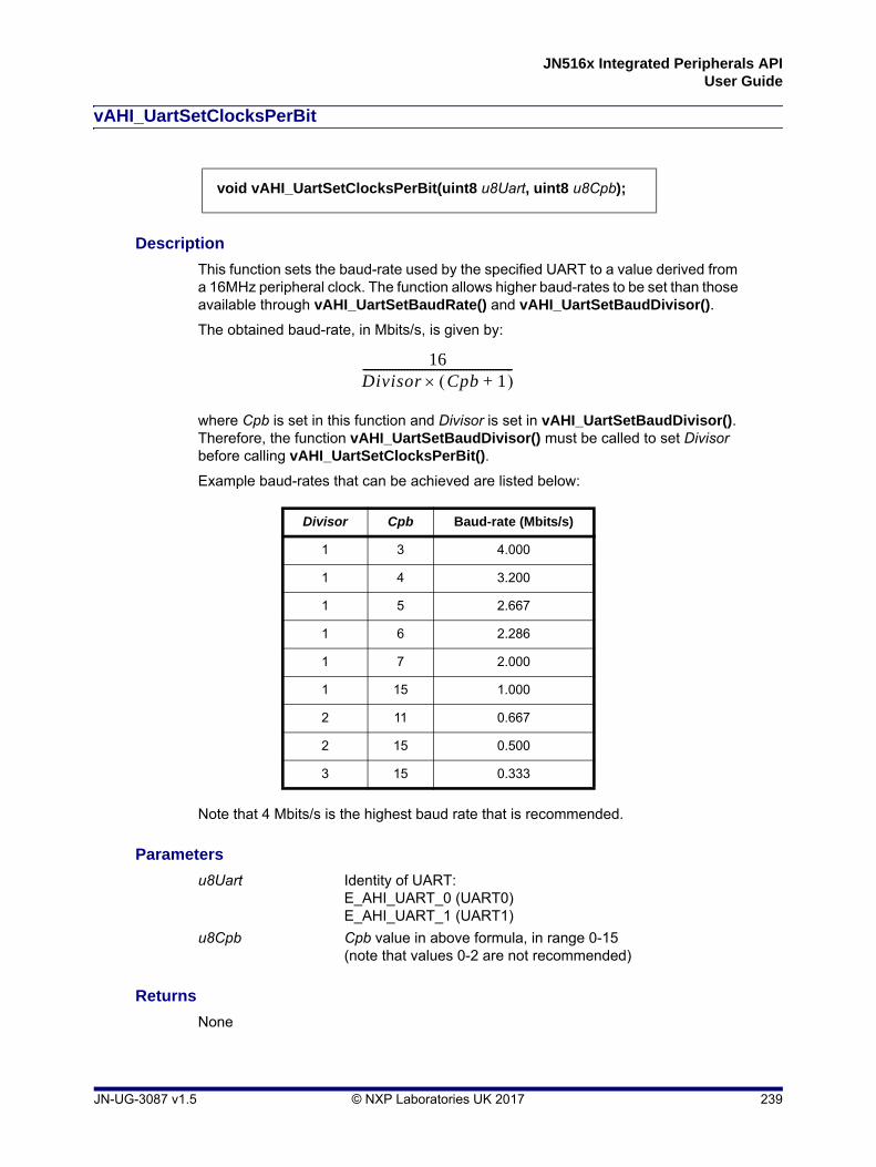
JN516x Integrated Peripherals APIUser Guide
vAHI_UartSetClocksPerBit
Description
This function sets the baud-rate used by the specified UART to a value derived from a 16MHz peripheral clock. The function allows higher baud-rates to be set than those available through vAHI_UartSetBaudRate() and vAHI_UartSetBaudDivisor().
The obtained baud-rate, in Mbits/s, is given by:
where Cpb is set in this function and Divisor is set in vAHI_UartSetBaudDivisor(). Therefore, the function vAHI_UartSetBaudDivisor() must be called to set Divisor before calling vAHI_UartSetClocksPerBit().
Example baud-rates that can be achieved are listed below:
Note that 4 Mbits/s is the highest baud rate that is recommended.
Parameters
u8Uart Identity of UART: E_AHI_UART_0 (UART0)E_AHI_UART_1 (UART1)
u8Cpb Cpb value in above formula, in range 0-15(note that values 0-2 are not recommended)
Returns
None
void vAHI_UartSetClocksPerBit(uint8 u8Uart, uint8 u8Cpb);
Divisor Cpb Baud-rate (Mbits/s)
1 3 4.000
1 4 3.200
1 5 2.667
1 6 2.286
1 7 2.000
1 15 1.000
2 11 0.667
2 15 0.500
3 15 0.333
16Divisor Cpb 1+ ---------------------------------------------------
JN-UG-3087 v1.5 © NXP Laboratories UK 2017 239
Chapter 22UART Functions
vAHI_UartSetControl
Description
This function sets various control bits for the specified UART.
Note that RTS for UART0 cannot be controlled automatically - it can only be set/cleared under software control (this setting will be ignored for UART1).
Parameters
u8Uart Identity of UART: E_AHI_UART_0 (UART0)E_AHI_UART_1 (UART1)
bEvenParity Type of parity to be applied (if enabled):E_AHI_UART_EVEN_PARITY (even parity)E_AHI_UART_ODD_PARITY (odd parity)
bEnableParity Enable/disable parity check:E_AHI_UART_PARITY_ENABLEE_AHI_UART_PARITY_DISABLE
u8WordLength Word length (in bits):E_AHI_UART_WORD_LEN_5 (word is 5 bits)E_AHI_UART_WORD_LEN_6 (word is 6 bits)E_AHI_UART_WORD_LEN_7 (word is 7 bits)E_AHI_UART_WORD_LEN_8 (word is 8 bits)
bOneStopBit Number of stop bits - 1 stop bit, or 1.5 or 2 stop bits (depending on word length), enumerated as:E_AHI_UART_1_STOP_BIT (TRUE - 1 stop bit)E_AHI_UART_2_STOP_BITS (FALSE - 1.5 or 2 stop bits)
bRtsValue Set/clear RTS signal (UART0 only):E_AHI_UART_RTS_HIGH (TRUE - set RTS to high)E_AHI_UART_RTS_LOW (FALSE - clear RTS to low)
Returns
None
void vAHI_UartSetControl(uint8 u8Uart, bool_t bEvenParity, bool_t bEnableParity, uint8 u8WordLength, bool_t bOneStopBit, bool_t bRtsValue);
240 © NXP Laboratories UK 2017 JN-UG-3087 v1.5
JN516x Integrated Peripherals APIUser Guide
vAHI_UartSetInterrupt
Description
This function enables or disables the interrupts generated by the specified UART and sets the Receive FIFO trigger-level - that is, the number of bytes required in the Receive FIFO to trigger a ‘receive data available’ interrupt.
Parameters
u8Uart Identity of UART: E_AHI_UART_0 (UART0)E_AHI_UART_1 (UART1)
bEnableModemStatus Enable/disable ‘modem status’ interrupt (e.g. CTS change detected for UART0):TRUE to enableFALSE to disable
bEnableRxLineStatus Enable/disable ‘receive line status’ interrupt (break indication, framing error, parity error or over-run):TRUE to enableFALSE to disable
bEnableTxFifoEmpty Enable/disable ‘Transmit FIFO empty’ interrupt:TRUE to enableFALSE to disable
bEnableRxData Enable/disable ‘receive data available’ interrupt:TRUE to enableFALSE to disable
u8FifoLevel Number of bytes in Receive FIFO required to trigger a ‘receive data available’ interrupt:E_AHI_UART_FIFO_LEVEL_1 (1 byte)E_AHI_UART_FIFO_LEVEL_4 (4 bytes)E_AHI_UART_FIFO_LEVEL_8 (8 bytes)E_AHI_UART_FIFO_LEVEL_14 (14 bytes)
Returns
None
void vAHI_UartSetInterrupt(uint8 u8Uart, bool_t bEnableModemStatus, bool_t bEnableRxLineStatus, bool_t bEnableTxFifoEmpty, bool_t bEnableRxData, uint8 u8FifoLevel);
JN-UG-3087 v1.5 © NXP Laboratories UK 2017 241

Chapter 22UART Functions
vAHI_UartTxOnly
Description
This function enables or disables 1-wire mode on the specified UART. In this mode, the UART can only transmit - only the TxD pin is used and the RxD is released for other uses.
Parameters
u8Uart Identity of UART: E_AHI_UART_0 (UART0)E_AHI_UART_1 (UART1)
bEnable Enable/disable 1-wire mode:TRUE to enableFALSE to disable
Returns
None
void vAHI_UartTxOnly(uint8 u8Uart, bool_t bEnable);
Note: Currently, 1-wire mode is supported on UART1 only and this function will have no effect if UART0 is specified.
242 © NXP Laboratories UK 2017 JN-UG-3087 v1.5

JN516x Integrated Peripherals APIUser Guide
vAHI_UartSetRTSCTS
Description
This function instructs UART0 to take or release control of the DIO lines used for RTS and CTS in flow control (depending on the DIOs selected):
DIO4 (default) or DIO12 for CTS
DIO5 (default) or DIO13 for RTS
The function must be called before vAHI_UartEnable() is called.
UART0 operates by default in 4-wire mode. If you wish to use this UART in 2-wire mode, it will be necessary to call vAHI_UartSetRTSCTS() before calling bAHI_UartEnable() in order to release control of the RTS and CTS lines.
Parameters
u8Uart Identity of UART: set to E_AHI_UART_0
bRTSCTSEn Take/release control of DIO lines for RTS and CTS:TRUE to take controlFALSE to release control (allow use for other operations)
Returns
None
void vAHI_UartSetRTSCTS(uint8 u8Uart, bool_t bRTSCTSEn);
JN-UG-3087 v1.5 © NXP Laboratories UK 2017 243
Chapter 22UART Functions
vAHI_UartSetRTS
Description
This function instructs UART0 to set or clear its RTS signal in 4-wire mode.
In order to use this function, the UART must be in 4-wire mode without automatic flow control enabled.
The function must be called after bAHI_UartEnable() is called.
Parameters
u8Uart Identity of UART: set to E_AHI_UART_0
bRtsValue Set/clear RTS signal:E_AHI_UART_RTS_HIGH (TRUE - set RTS to high)E_AHI_UART_RTS_LOW (FALSE - clear RTS to low)
Returns
None
void vAHI_UartSetRTS(uint8 u8Uart, bool_t bRtsValue);
244 © NXP Laboratories UK 2017 JN-UG-3087 v1.5

JN516x Integrated Peripherals APIUser Guide
vAHI_UartSetAutoFlowCtrl
Description
This function allows Automatic Flow Control (AFC) to be configured and enabled for UART0 operating in 4-wire mode. The function parameters allow the following to be selected/set:
Automatic RTS (bAutoRts): This is the automatic control of the outgoing RTS signal based on the Receive FIFO fill-level. RTS is de-asserted when the Receive FIFO fill-level is greater than or equal to the specified trigger level (u8RxFifoLevel). RTS is then re-asserted as soon as Receive FIFO fill-level falls below the trigger level.
Automatic CTS (bAutoCts): This is the automatic control of transmissions based on the incoming CTS signal. The transmission of a character is only started if the CTS input is asserted.
Receive FIFO Automatic RTS trigger level (u8RxFifoLevel): This is the level at which the outgoing RTS signal is de-asserted when the Automatic RTS feature is enabled (using bAutoRts). If using a USB/FTDI cable to connect to the UART, use a setting of 13 bytes or lower (otherwise the Receive FIFO will overflow and data will be lost, as the FTDI device sends up to 3 bytes of data even once RTS has been de-asserted).
Flow Control Polarity (bFlowCtrlPolarity): This is the active level (active-low or active-high) of the RTS and CTS hardware flow control signals when using the AFC feature. This setting has no effect when not using AFC (in this case, the software decides the active level, sets the outgoing RTS value and monitors the incoming CTS value).
In order to use the RTS and CTS lines, UART0 must be enabled in 4-wire mode, which is its default mode.
Parameters
u8Uart Identity of UART: set to E_AHI_UART_0
u8RxFifoLevel Receive FIFO automatic RTS trigger level:E_AHI_UART_FIFO_ARTS_LEVEL_8: 8 bytesE_AHI_UART_FIFO_ARTS_LEVEL_11: 11 bytesE_AHI_UART_FIFO_ARTS_LEVEL_13: 13 bytesE_AHI_UART_FIFO_ARTS_LEVEL_15: 15 bytes
bFlowCtrlPolarity Active level (low or high) of RTS and CTS flow control:FALSE: RTS and CTS are active-lowTRUE: RTS and CTS are active-high
bAutoRts Enable/disable Automatic RTS feature:TRUE to enableFALSE to disable
bAutoCts Enable/disable Automatic CTS feature:TRUE to enableFALSE to disable
void vAHI_UartSetAutoFlowCtrl(uint8 u8Uart,uint8 u8RxFifoLevel,bool_t bFlowCtrlPolarity,bool_t bAutoRts,bool_t bAutoCts);
JN-UG-3087 v1.5 © NXP Laboratories UK 2017 245

Chapter 22UART Functions
Returns
None
246 © NXP Laboratories UK 2017 JN-UG-3087 v1.5

JN516x Integrated Peripherals APIUser Guide
vAHI_UartSetBreak
Description
This function instructs the specified UART to initiate or clear a transmission break.
On setting the break condition using this function, the data byte that is currently being transmitted is corrupted and transmission then stops. On clearing the break condition, transmission resumes to transfer the data remaining in the Transmit FIFO.
Parameters
u8Uart Identity of UART: E_AHI_UART_0 (UART0)E_AHI_UART_1 (UART1)
bBreak Instruction for UART:TRUE to initiate break (no data)FALSE to clear break (and resume data transmission)
Returns
None
void vAHI_UartSetBreak(uint8 u8Uart, bool_t bBreak);
JN-UG-3087 v1.5 © NXP Laboratories UK 2017 247

Chapter 22UART Functions
vAHI_UartReset
Description
This function resets the Transmit and Receive FIFOs of the specified UART. The character currently being transferred is not affected. The Transmit and Receive FIFOs can be reset individually or together.
The function also sets the FIFO trigger-level to single-byte trigger. The Receive FIFO interrupt trigger-level can be set via vAHI_UartSetInterrupt().
Parameters
u8Uart Identity of UART: E_AHI_UART_0 (UART0)E_AHI_UART_1 (UART1)
bTxReset Transmit FIFO reset:TRUE to reset the Transmit FIFOFALSE not to reset the Transmit FIFO
bRxReset Receive FIFO reset:TRUE to reset the Receive FIFOFALSE not to reset the Receive FIFO
Returns
None
void vAHI_UartReset(uint8 u8Uart, bool_t bTxReset, bool_t bRxReset);
248 © NXP Laboratories UK 2017 JN-UG-3087 v1.5

JN516x Integrated Peripherals APIUser Guide
u16AHI_UartReadRxFifoLevel
Description
This function obtains the fill-level of the Receive FIFO of the specified UART - that is, the number of characters currently in the FIFO.
Parameters
u8Uart Identity of UART: E_AHI_UART_0 (UART0)E_AHI_UART_1 (UART1)
Returns
Number of characters in the specified Receive FIFO
uint16 u16AHI_UartReadRxFifoLevel(uint8 u8Uart);
JN-UG-3087 v1.5 © NXP Laboratories UK 2017 249

Chapter 22UART Functions
u16AHI_UartReadTxFifoLevel
Description
This function obtains the fill-level of the Transmit FIFO - that is, the number of characters currently in the FIFO.
Parameters
u8Uart Identity of UART: E_AHI_UART_0 (UART0)E_AHI_UART_1 (UART1)
Returns
Number of characters in the specified Transmit FIFO
uint16 u16AHI_UartReadTxFifoLevel(uint8 u8Uart);
250 © NXP Laboratories UK 2017 JN-UG-3087 v1.5

JN516x Integrated Peripherals APIUser Guide
u8AHI_UartReadRxFifoLevel
Description
This function obtains the fill-level of the Receive FIFO of the specified UART on the JN516x device - that is, the number of characters currently in the FIFO.
Parameters
u8Uart Identity of UART: E_AHI_UART_0 (UART0)E_AHI_UART_1 (UART1)
Returns
Number of characters in the specified Receive FIFO
uint8 u8AHI_UartReadRxFifoLevel(uint8 u8Uart);
Note: This function is provided only for backward compatibility with application code developed for the JN514x microcontrollers. New code for the JN516x microcontrollers should use the function u16AHI_UartReadRxFifoLevel() instead, described on page 249.
JN-UG-3087 v1.5 © NXP Laboratories UK 2017 251

Chapter 22UART Functions
u8AHI_UartReadTxFifoLevel
Description
This function obtains the fill-level of the Transmit FIFO of the specified UART on the JN516x device - that is, the number of characters currently in the FIFO.
Parameters
u8Uart Identity of UART: E_AHI_UART_0 (UART0)E_AHI_UART_1 (UART1)
Returns
Number of characters in the specified Transmit FIFO
uint8 u8AHI_UartReadTxFifoLevel(uint8 u8Uart);
Note: This function is provided only for backward compatibility with application code developed for the JN514x microcontrollers. New code for the JN516x microcontrollers should use the function u16AHI_UartReadTxFifoLevel() instead, described on page 250.
252 © NXP Laboratories UK 2017 JN-UG-3087 v1.5

JN516x Integrated Peripherals APIUser Guide
u8AHI_UartReadLineStatus
Description
This function returns line status information in a bitmap for the specified UART.
Note that the following bits are cleared after reading:
E_AHI_UART_LS_ERROR E_AHI_UART_LS_BI E_AHI_UART_LS_FE E_AHI_UART_LS_PE E_AHI_UART_LS_OE
Parameters
u8Uart Identity of UART: E_AHI_UART_0 (UART0)E_AHI_UART_1 (UART1)
Returns
Bitmap:
uint8 u8AHI_UartReadLineStatus(uint8 u8Uart);
Bit Description
E_AHI_UART_LS_ERROR This bit will be set if a parity error, framing error or break indication has been received
E_AHI_UART_LS_TEMT This bit will be set if the Transmit Shift Register is empty
E_AHI_UART_LS_THRE This bit will be set if the Transmit FIFO is empty
E_AHI_UART_LS_BI This bit will be set if a break indication has been received (line held low for a whole character)
E_AHI_UART_LS_FE This bit will be set if a framing error has been received
E_AHI_UART_LS_PE This bit will be set if a parity error has been received
E_AHI_UART_LS_OE This bit will be set if a receive over-run has occurred, i.e. the receive buffer is full but another character arrives
E_AHI_UART_LS_DR This bit will be set if there is data in the Receive FIFO
JN-UG-3087 v1.5 © NXP Laboratories UK 2017 253

Chapter 22UART Functions
u8AHI_UartReadModemStatus
Description
This function obtains modem status information from UART0 as a bitmap which includes the CTS and ‘CTS has changed’ status (which can be extracted as described below).
Parameters
u8Uart Identity of UART: set to E_AHI_UART_0
Returns
Bitmap in which:
CTS input status is bit 4 (‘1’ indicates CTS is high, ‘0’ indicates CTS is low).
‘CTS has changed’ status is bit 0 (‘1’ indicates that CTS input has changed). If the return value bitwise ANDed with E_AHI_UART_MS_DCTS is non-zero, the CTS input has changed.
uint8 u8AHI_UartReadModemStatus(uint8 u8Uart);
254 © NXP Laboratories UK 2017 JN-UG-3087 v1.5

JN516x Integrated Peripherals APIUser Guide
u8AHI_UartReadInterruptStatus
Description
This function returns a pending interrupt for the specified UART as a bitmap.
Interrupts are returned one at a time, according to their priorities, so there may need to be multiple calls to this function. If interrupts are enabled, the interrupt handler processes this activity and posts each interrupt to the queue or to a callback function.
Parameters
u8Uart Identity of UART: E_AHI_UART_0 (UART0)E_AHI_UART_1 (UART1)
Returns
Bitmap:
The above table lists the UART interrupts (bits 1-3) from highest to lowest priority.
uint8 u8AHI_UartReadInterruptStatus(uint8 u8Uart);
Bit range Value/Enumeration Description
Bit 0 0 More interrupts pending
1 No more interrupts pending
Bits 1-3 E_AHI_UART_INT_RXLINE (3) Receive line status interrupt (highest prioritry)
E_AHI_UART_INT_RXDATA (2) Receive data available interrupt (next highest priority)
E_AHI_UART_INT_TIMEOUT (6) Timeout interrupt (next highest priority)
E_AHI_UART_INT_TX (1) Transmit FIFO empty interrupt (next highest priority)
E_AHI_UART_INT_MODEM (0) Modem status interrupt (lowest priority)
JN-UG-3087 v1.5 © NXP Laboratories UK 2017 255

Chapter 22UART Functions
vAHI_UartWriteData
Description
This function writes a data byte to the Transmit FIFO of the specified UART. The data byte will start to be transmitted as soon as it reaches the head of the FIFO.
If no flow control or manual flow control is being implemented for data transmission, the data in the Transmit FIFO will be transmitted as soon as possible (irrespective of the state of the local CTS line). Therefore, the function vAHI_UartWriteData() should be called only when the destination device is able to receive the data.
For UART0, if automatic flow control has been enabled for the local CTS line using the function vAHI_UartSetAutoFlowCtrl(), the data in the Transmit FIFO will only be transmitted once the CTS line has been asserted. In this case, vAHI_UartWriteData() can be called at any time to load data into the Transmit FIFO, provided that there is enough free space in the FIFO.
Refer to the description of u16AHI_UartReadTxFifoLevel() or u8AHI_UartReadLineStatus() for details of how to determine whether the Transmit FIFO already contains data.
Before this function is called, the UART must be enabled using the function bAHI_UartEnable(), otherwise an exception will result.
Parameters
u8Uart Identity of UART: E_AHI_UART_0 (UART0)E_AHI_UART_1 (UART1)
u8Data Byte to transmit
Returns
None
void vAHI_UartWriteData(uint8 u8Uart, uint8 u8Data);
256 © NXP Laboratories UK 2017 JN-UG-3087 v1.5
JN516x Integrated Peripherals APIUser Guide
u8AHI_UartReadData
Description
This function returns a single byte read from the Receive FIFO of the specified UART. If the FIFO is empty, the returned value is not valid.
Refer to the description of u16AHI_UartReadRxFifoLevel() or u8AHI_UartReadLineStatus() for details of how to determine whether the Receive FIFO is empty.
Parameters
u8Uart Identity of UART: E_AHI_UART_0 (UART0)E_AHI_UART_1 (UART1)
Returns
Received byte
uint8 u8AHI_UartReadData (uint8 u8Uart);
JN-UG-3087 v1.5 © NXP Laboratories UK 2017 257

Chapter 22UART Functions
u16AHI_UartBlockWriteData
Description
This function writes a block of data to the Transmit FIFO of the specified UART. The transmission of the data will then be handled by the on-chip DMA engine.
If no flow control or manual flow control is being implemented for data transmission, the data in the Transmit FIFO will be transmitted as soon as possible (irrespective of the state of the local CTS line). Therefore, u16AHI_UartBlockWriteData() should be called only when the destination device is able to receive the data.
For UART0, if automatic flow control has been enabled for the local CTS line using the function vAHI_UartSetAutoFlowCtrl(), the data in the Transmit FIFO will only be transmitted once the CTS line has been asserted. In this case, u16AHI_UartBlockWriteData() can be called at any time to load data into the Transmit FIFO, provided that there is enough free space in the FIFO.
Refer to the description of u16AHI_UartReadTxFifoLevel() or u8AHI_UartReadLineStatus() for details of how to determine whether the Transmit FIFO already contains data.
Before this function is called, the UART must be enabled using the function bAHI_UartEnable(), otherwise an exception will result.
Parameters
u8Uart Identity of UART: E_AHI_UART_0 (UART0)E_AHI_UART_1 (UART1)
*pu8Data Pointer to start of data block to be written to Transmit FIFO
u16DataLength Size of data block, in bytes
Returns
Number of bytes of data successfully written to the Transmit FIFO
uint16 u16AHI_UartBlockWriteData(uint8 u8Uart,uint8 *pu8Data,uint16 u16DataLength);
258 © NXP Laboratories UK 2017 JN-UG-3087 v1.5

JN516x Integrated Peripherals APIUser Guide
u16AHI_UartBlockReadData
Description
This function reads a block of data from the Receive FIFO of the specified UART. If the FIFO is empty, the returned value is not valid.
A data buffer in RAM to receive the read data block must be specified.
Refer to the description of u16AHI_UartReadRxFifoLevel() or u8AHI_UartReadLineStatus() for details of how to determine whether the Receive FIFO is empty.
Parameters
u8Uart Identity of UART: E_AHI_UART_0 (UART0)E_AHI_UART_1 (UART1)
*pu8DataBuffer Pointer to data buffer in RAM to receive read data block
u16DataBufferLength Size of data buffer, in bytes
Returns
Number of bytes of data successfully read from Receive FIFO
uint16 u16AHI_UartBlockReadData(uint8 u8Uart,uint8 *pu8DataBuffer,uint16 u16DataBufferLength);
JN-UG-3087 v1.5 © NXP Laboratories UK 2017 259
Chapter 22UART Functions
vAHI_Uart0RegisterCallback
Description
This function registers a user-defined callback function that will be called when the UART0 interrupt is triggered.
The registered callback function is only preserved during sleep modes in which RAM remains powered. If RAM is powered off during sleep and interrupts are required, the callback function must be re-registered before calling u32AHI_Init() on waking.
Interrupt handling is described in Appendix A.
Parameters
prUart0Callback Pointer to callback function to be registered
Returns
None
void vAHI_Uart0RegisterCallback(PR_HWINT_APPCALLBACK prUart0Callback);
260 © NXP Laboratories UK 2017 JN-UG-3087 v1.5

JN516x Integrated Peripherals APIUser Guide
vAHI_Uart1RegisterCallback
Description
This function registers a user-defined callback function that will be called when the UART1 interrupt is triggered.
The registered callback function is only preserved during sleep modes in which RAM remains powered. If RAM is powered off during sleep and interrupts are required, the callback function must be re-registered before calling u32AHI_Init() on waking.
Interrupt handling is described in Appendix A.
Parameters
prUart1Callback Pointer to callback function to be registered
Returns
None
void vAHI_Uart1RegisterCallback(PR_HWINT_APPCALLBACK prUart1Callback);
JN-UG-3087 v1.5 © NXP Laboratories UK 2017 261

Chapter 22UART Functions
262 © NXP Laboratories UK 2017 JN-UG-3087 v1.5
JN516x Integrated Peripherals APIUser Guide
23. Timer Functions
This chapter describes the functions that can be used to control the on-chip timers. The JN516x device has five times: Timer 0, Timer 1, Timer 2, Timer 3 and Timer 4(Timers 1-4 have no external inputs and only support modes without inputs)
They are distinct from the wake timers described in Chapter 8 and tick timer described in Chapter 9.
The Timer functions are listed below, along with their page references:
Function Page
vAHI_TimerEnable 264
vAHI_TimerClockSelect 266
vAHI_TimerConfigureOutputs 267
vAHI_TimerConfigureInputs 268
vAHI_TimerSetLocation 269
vAHI_TimerStartSingleShot 270
vAHI_TimerStartRepeat 271
vAHI_TimerStartCapture 272
vAHI_TimerStartDeltaSigma 273
u16AHI_TimerReadCount 275
vAHI_TimerReadCapture 276
vAHI_TimerReadCaptureFreeRunning 277
vAHI_TimerStop 278
vAHI_TimerDisable 279
vAHI_TimerDIOControl 280
vAHI_TimerFineGrainDIOControl 281
u8AHI_TimerFired 282
vAHI_Timer0RegisterCallback 283
vAHI_Timer1RegisterCallback 284
vAHI_Timer2RegisterCallback 285
vAHI_Timer3RegisterCallback 286
vAHI_Timer4RegisterCallback 287
Note: For information on the timers and guidance on using the timer functions in JN516x application code, refer to Chapter 7.
JN-UG-3087 v1.5 © NXP Laboratories UK 2017 263

Chapter 23Timer Functions
vAHI_TimerEnable
Description
This function configures and enables the specified timer, and must be the first timer function called. The timer is derived from the peripheral clock, which can be divided down to produce the timer clock (a system clock sourced from the external crystal oscillator gives the most stable results). The timer can be used in various modes, introduced in Section 7.1 (note that Timers 1-4 have no external inputs and therefore only support modes without inputs).
The parameters of this enable function cover the following features:
Prescaling (u8Prescale): The timer’s source clock is divided down to produce a slower clock for the timer, the divisor being 2u8Prescale. Therefore:
Timer clock frequency = Source clock frequency / 2u8Prescale
Interrupts (bIntRiseEnable and bIntPeriodEnable): Interrupts can be generated:
in Timer or PWM mode, on a low-to-high transition (rising output) and/or on a high-to-low transition (end of the timer period)
in Counter mode, on reaching target counts
You can register a user-defined callback function for timer interrupts using the function vAHI_Timer0RegisterCallback() for Timer 0, vAHI_Timer1RegisterCallback() for Timer 1, vAHI_Timer2RegisterCallback() for Timer 2, vAHI_Timer3RegisterCallback() for Timer 3 or vAHI_Timer4RegisterCallback() for Timer 4. Alternatively, timer interrupts can be disabled.
Timer output (bOutputEnable): When operating in PWM mode or Delta-Sigma mode, the timer’s signal is output on a DIO pin (see Section 7.2.1), which must be enabled. If this option is enabled, the other DIOs associated with the timer cannot be used for general-purpose input/output.
Parameters
u8Timer Identity of timer: E_AHI_TIMER_0 (Timer 0)E_AHI_TIMER_1 (Timer 1)E_AHI_TIMER_2 (Timer 2)E_AHI_TIMER_3 (Timer 3)E_AHI_TIMER_4 (Timer 4)
u8Prescale Prescale index, in range 0 to 16, used in dividing down source clock (divisor is 2u8Prescale)
bIntRiseEnable Enable/disable interrupt on rising output (low-to-high):TRUE to enableFALSE to disable
bIntPeriodEnable Enable/disable interrupt at end of timer period (high-to-low):TRUE to enableFALSE to disable
void vAHI_TimerEnable(uint8 u8Timer, uint8 u8Prescale, bool_t bIntRiseEnable, bool_t bIntPeriodEnable, bool_t bOutputEnable);
264 © NXP Laboratories UK 2017 JN-UG-3087 v1.5

JN516x Integrated Peripherals APIUser Guide
bOutputEnable Enable/disable output of timer signal on DIO:TRUE to enable (PWM or Delta-Sigma mode)FALSE to disable (Timer mode)
Returns
None
JN-UG-3087 v1.5 © NXP Laboratories UK 2017 265

Chapter 23Timer Functions
vAHI_TimerClockSelect
Description
This function can be used to enable/disable an external clock input for Timer 0. If enabled, the external input is taken from the DIO8 pin.
Note the following:
This function should only be called when using the timer in Counter mode - in this mode, the timer is used to count edges on an input clock or pulse train.
Output gating can be enabled when the internal clock is used.
If required, this function must be called after vAHI_TimerEnable().
Parameters
u8Timer Identity of timer: set to E_AHI_TIMER_0
bExternalClock Clock source: TRUE to use an external source (Counter mode only)FALSE to use the internal 16MHz clock
bInvertClock TRUE to gate the output pin when the gate input is high and invert the clockFALSE to gate the output pin when the gate input is low and not invert the clock
Returns
None
void vAHI_TimerClockSelect(uint8 u8Timer, bool_t bExternalClock, bool_t bInvertClock);
266 © NXP Laboratories UK 2017 JN-UG-3087 v1.5

JN516x Integrated Peripherals APIUser Guide
vAHI_TimerConfigureOutputs
Description
This function configures certain parameters relating to the operation of the specified timer in the following modes (introduced in Section 7.1):
Timer mode: The internal peripheral clock drives the timer’s counter in order to produce a pulse cycle in either ‘single shot’ or ‘repeat’ mode. The clock may be temporarily interrupted by a gating input on a DIO (see Section 7.2.1 for the relevant DIOs). Clock gating can be enabled/disabled using this function for Timer 0 only (there are no gating inputs for Timers 1-4).
Pulse Width Modulation (PWM) mode: The PWM signal produced in Timer mode (see above) is output, where this output can be enabled in vAHI_TimerEnable(). The signal is output on a DIO which depends on the timer selected (see Section 7.2.1 for the relevant DIOs). If required, the output signal can be inverted using this function on any of the timers operating in PWM mode.
This function must be called after the specified timer has been enabled through vAHI_TimerEnable() and before the timer is started.
Parameters
u8Timer Identity of timer: E_AHI_TIMER_0 (Timer 0)E_AHI_TIMER_1 (Timer 1)E_AHI_TIMER_2 (Timer 2)E_AHI_TIMER_3 (Timer 3)E_AHI_TIMER_4 (Timer 4)
bInvertPwmOutput Enable/disable inversion of PWM output:TRUE to enable inversionFALSE to disable inversion
bGateDisable Enable/disable external gating input for Timer mode:TRUE to disable clock gating inputFALSE to enable clock gating input(for Timers 1-4, set to TRUE)
Returns
None
void vAHI_TimerConfigureOutputs(uint8 u8Timer, bool_t bInvertPwmOutput,bool_t bGateDisable);
JN-UG-3087 v1.5 © NXP Laboratories UK 2017 267

Chapter 23Timer Functions
vAHI_TimerConfigureInputs
Description
This function configures certain parameters relating to the operation of Timer 0 (there are no external signal inputs for Timers 1-4) in the following modes (introduced in Section 7.1):
Capture mode: An external signal is sampled on every tick of the timer. The results of the capture allow the period and pulse width of the sampled signal to be obtained. The input signal can be inverted using this function, allowing the low-pulse width to be measured (instead of the high-pulse width). This external signal is input on the DIO9 pin.
Counter mode: The timer is used to count the number of transitions on an external input (selected using vAHI_TimerClockSelect()). This configure function allows selection of the transitions on which the count will be performed - on low-to-high transitions, or on both low-to-high and high-to-low transitions.
This function must be called after the timer has been enabled through vAHI_TimerEnable() and before the timer is started.
Parameters
u8Timer Identity of timer: set to E_AHI_TIMER_0
bInvCapt Enable/disable inversion of the capture input signal:TRUE to enable inversionFALSE to disable inversion
bEventEdge Determines the edge(s) of the external input on which the count will be incremented in counter mode:TRUE - on both low-to-high and high-to-low transitionsFALSE - on low-to-high transition
Returns
None
void vAHI_TimerConfigureInputs(uint8 u8Timer, bool_t bInvCapt,bool_t bEventEdge);
268 © NXP Laboratories UK 2017 JN-UG-3087 v1.5

JN516x Integrated Peripherals APIUser Guide
vAHI_TimerSetLocation
Description
This function can be used to select the set of pins on which the specified timer(s) will operate. The affected timers can be Timer 0 alone or the other four timers (1, 2, 3 and 4) collectively:
Timer 0 can use DIO8-10 (default) or alternatively DIO2-4
Timers 1, 2, 3 and 4 can use DIO11-13 and 17 (default) or alternatively DIO5-8
Note that specifying any one of Timers 1-4 in the bLocation parameter will relocate the DIOs for all four of these timers. However, it is possible to relocate Timer 3 onto DO1 and Timer 2 onto DO0 (Digital Output 1 and Digital Output 0, and not DIOs) using the bLocationOverridePWM3andPWM2 parameter, which over-rides the bLocation setting for these two timers.
The function only needs to be called if the alternative DIOs are preferred.
Parameters
u8Timer Timer(s) to which DIO re-location will be applied:E_AHI_TIMER_0 (Timer 0)E_AHI_TIMER_1 (Timers 1-4)E_AHI_TIMER_2 (Timers 1-4)E_AHI_TIMER_3 (Timers 1-4)E_AHI_TIMER_4 (Timers 1-4)
bLocation DIOs on which specified timer(s) will operate:TRUE - DIO2-4 (Timer 0) or DIO5-8 (Timers 1-4)FALSE - DIO8-10 (Timer 0) or DIO11-13 & 17 (Timers 1-4)
bLocationOverridePWM3andPWM2
Relocate Timers 3 and 2 onto DO1 and DO0:TRUE - relocate to DO1 and DO0FALSE - relocate as specified by bLocation
Returns
None
void vAHI_TimerSetLocation(uint8 u8Timer, bool_t bLocation,bool_t bLocationOverridePWM3andPWM2);
JN-UG-3087 v1.5 © NXP Laboratories UK 2017 269

Chapter 23Timer Functions
vAHI_TimerStartSingleShot
Description
This function starts the specified timer in ‘single-shot’ mode. The function relates to Timer mode, PWM mode and Counter mode (introduced in Section 7.1).
In Timer or PWM mode, during one pulse cycle produced, the timer signal starts low and then goes high:
1. The output is low until u16Hi clock periods have passed, when it goes high.
2. The output remains high until u16Lo clock periods have passed since the timer was started and then goes low again (marking the end of the pulse cycle).
If enabled through vAHI_TimerEnable(), an interrupt can be triggered at the low-high transition and/or the high-low transition.
In Counter mode, this function is used differently:
At a count of u16Hi, an interrupt (E_AHI_TIMER_RISE_MASK) will be generated (if enabled).
At a count of u16Lo, another interrupt (E_AHI_TIMER_PERIOD_MASK) will be generated (if enabled) and the timer will stop.
Again, interrupts are enabled through vAHI_TimerEnable().
Note that Counter mode is only available for Timer 0.
Parameters
u8Timer Identity of timer: E_AHI_TIMER_0 (Timer 0)E_AHI_TIMER_1 (Timer 1)E_AHI_TIMER_2 (Timer 2)E_AHI_TIMER_3 (Timer 3)E_AHI_TIMER_4 (Timer 4)
u16Hi Number of clock periods after starting a timer before the output goes high (Timer or PWM mode) or count at which first interrupt generated (Counter mode)
u16Lo Number of clock periods after starting a timer before the output goes low again (Timer or PWM mode) or count at which second interrupt generated and timer stops (Counter mode)
Returns
None
void vAHI_TimerStartSingleShot(uint8 u8Timer, uint16 u16Hi, uint16 u16Lo);
270 © NXP Laboratories UK 2017 JN-UG-3087 v1.5

JN516x Integrated Peripherals APIUser Guide
vAHI_TimerStartRepeat
Description
This function starts the specified timer in ‘repeat’ mode. The function relates to Timer mode, PWM mode and Counter mode (introduced in Section 7.1).
In Timer or PWM mode, during each pulse cycle produced, the timer signal starts low and then goes high:
1. The output is low until u16Hi clock periods have passed, when it goes high.
2. The output remains high until u16Lo clock periods have passed since the timer was started and then goes low again.
The above process repeats until the timer is stopped using vAHI_TimerStop().
If enabled through vAHI_TimerEnable(), an interrupt can be triggered at the low-high transition and/or the high-low transition.
In Counter mode, this function is used differently:
At a count of u16Hi, an interrupt (E_AHI_TIMER_RISE_MASK) will be generated (if enabled).
At a count of u16Lo, another interrupt (E_AHI_TIMER_PERIOD_MASK) will be generated (if enabled) and the count will then be re-started from zero.
Again, interrupts are enabled through vAHI_TimerEnable().
The current count can be read at any time using u16AHI_TimerReadCount().
Note that Counter mode is only available for Timer 0.
Parameters
u8Timer Identity of timer: E_AHI_TIMER_0 (Timer 0)E_AHI_TIMER_1 (Timer 1)E_AHI_TIMER_2 (Timer 2)E_AHI_TIMER_3 (Timer 3)E_AHI_TIMER_4 (Timer 4)
u16Hi Number of clock periods after starting a timer before the output goes high (Timer or PWM mode) or count at which first interrupt generated (Counter mode)
u16Lo Number of clock periods after starting a timer before the output goes low again (Timer or PWM mode) or count at which second interrupt generated (Counter mode)
Returns
None
void vAHI_TimerStartRepeat(uint8 u8Timer, uint16 u16Hi, uint16 u16Lo);
JN-UG-3087 v1.5 © NXP Laboratories UK 2017 271
Chapter 23Timer Functions
vAHI_TimerStartCapture
Description
This function starts Timer 0 in Capture mode (Timers 1-4 cannot operate in Capture mode). This mode must first be configured using the function vAHI_TimerConfigureInputs().
An input signal must be provided on the DIO9 pin. The incoming signal is timed and the captured measurements are:
number of clock cycles to the last low-to-high transition of the input signal
number of clock cycles to the last high-to-low transition of the input signal
These values are placed in registers to be read later using the function vAHI_TimerReadCapture() or vAHI_TimerReadCaptureFreeRunning(). They allow the input pulse width to be determined.
Parameters
u8Timer Identity of timer: set to E_AHI_TIMER_0
Returns
None
void vAHI_TimerStartCapture(uint8 u8Timer);
272 © NXP Laboratories UK 2017 JN-UG-3087 v1.5

JN516x Integrated Peripherals APIUser Guide
vAHI_TimerStartDeltaSigma
Description
This function starts the specified timer in Delta-Sigma mode, which allows the timer to be used as a low-rate DAC.
To use this mode, the DIO output for the timer (see Section 7.2.1 for the relevant DIOs) must be enabled through vAHI_TimerEnable(). In addition, an RC circuit must be inserted on the DIO output pin in the arrangement shown below (also see Note below).
The 16MHz peripheral clock is used as the timer source and the conversion period of the ‘DAC’ is 65536 clock cycles. In Delta-Sigma mode, the timer outputs a number of randomly spaced clock pulses as specified by the value being converted. When RC-filtered, this produces an analogue voltage proportional to the conversion value.
If the RTZ (Return-to-Zero) option is enabled, a low clock cycle is inserted after every clock cycle, so that there are never two consecutive high clock cycles. This doubles the conversion period, but improves linearity if the rise and fall times of the outputs are different from one another.
void vAHI_TimerStartDeltaSigma(uint8 u8Timer, uint16 u16Hi, uint16 0x0000, bool_t bRtzEnable);
Note: For more information on ‘Delta-Sigma’ mode, refer to the data sheet for your microcontroller.
R
C
DIO Vout
JN-UG-3087 v1.5 © NXP Laboratories UK 2017 273
Chapter 23Timer Functions
Parameters
u8Timer Identity of timer: E_AHI_TIMER_0 (Timer 0)E_AHI_TIMER_1 (Timer 1)E_AHI_TIMER_2 (Timer 2)E_AHI_TIMER_3 (Timer 3)E_AHI_TIMER_4 (Timer 4)
u16Hi Number of 16MHz clock cycles for which the output will be high during a conversion period, in the range 0 to 65535 (full period is 65536 clock cycles)
0x0000 Fixed null value
bRtzEnable Enable/disable RTZ (Return-to-Zero) option:TRUE to enableFALSE to disable
Returns
None
274 © NXP Laboratories UK 2017 JN-UG-3087 v1.5

JN516x Integrated Peripherals APIUser Guide
u16AHI_TimerReadCount
Description
This function obtains the current count value of the specified timer.
Parameters
u8Timer Identity of timer: E_AHI_TIMER_0 (Timer 0)E_AHI_TIMER_1 (Timer 1)E_AHI_TIMER_2 (Timer 2)E_AHI_TIMER_3 (Timer 3)E_AHI_TIMER_4 (Timer 4)
Returns
Current count value of timer
uint16 u16AHI_TimerReadCount(uint8 u8Timer);
JN-UG-3087 v1.5 © NXP Laboratories UK 2017 275

Chapter 23Timer Functions
vAHI_TimerReadCapture
Description
This function stops Timer 0 and then obtains the results from a 'capture' started using the function vAHI_TimerStartCapture().
The values returned are offsets from the start of capture, as follows:
number of clock cycles to the last low-to-high transition of the input signal
number of clock cycles to the last high-to-low transition of the input signal
The width of the last pulse can be calculated from the difference of these results, provided that the results were requested during a low period. However, since it is not possible to be sure of this, the results obtained from this function may not always be valid for calculating the pulse width.
If you wish to measure the pulse period of the input signal, you should use the function vAHI_TimerReadCaptureFreeRunning(), which does not stop the timer.
Capture mode and this function are relevant to Timer 0 only.
Parameters
u8Timer Identity of timer: set to E_AHI_TIMER_0
*pu16Hi Pointer to location which will receive clock period at which last low-high transition occurred
*pu16Lo Pointer to location which will receive clock period at which last high-low transition occurred
Returns
None
void vAHI_TimerReadCapture(uint8 u8Timer, uint16 *pu16Hi,uint16 *pu16Lo);
276 © NXP Laboratories UK 2017 JN-UG-3087 v1.5
JN516x Integrated Peripherals APIUser Guide
vAHI_TimerReadCaptureFreeRunning
Description
This function obtains the results from a 'capture' started on Timer 0 using the function vAHI_TimerStartCapture(). This function does not stop the timer.
Alternatively, the function vAHI_TimerReadCapture() can be used, which stops the timer before reporting the capture measurements.
The values returned are offsets from the start of capture, as follows:
number of clock cycles to the last low-to-high transition of the input signal
number of clock cycles to the last high-to-low transition of the input signal
The width of the last pulse can be calculated from the difference of these results, provided that the results were requested during a low period. However, since it is not possible to be sure of this, the results obtained from this function may not always be valid for calculating the pulse width.
If you wish to measure the pulse period of the input signal, you should call this function twice during consecutive pulse cycles. For example, a call to this function could be triggered by an interrupt generated on a particular type of transition (low-to-high or high-to-low). The pulse period can then be obtained by calculating the difference between the results for consecutive low-to-high transitions or the difference between the results for consecutive high-to-low transitions.
Capture mode and this function are relevant to Timer 0 only.
Parameters
u8Timer Identity of timer: set to E_AHI_TIMER_0
*pu16Hi Pointer to location which will receive clock period at which last low-high transition occurred
*pu16Lo Pointer to location which will receive clock period at which last high-low transition occurred
Returns
None
void vAHI_TimerReadCaptureFreeRunning(uint8 u8Timer, uint16 *pu16Hi, uint16 *pu16Lo);
Caution: Since it is not possible to be sure of the state of the input signal when capture started, the results of the first call to this function after starting capture should be discarded.
JN-UG-3087 v1.5 © NXP Laboratories UK 2017 277
Chapter 23Timer Functions
vAHI_TimerStop
Description
This function stops the specified timer.
Parameters
u8Timer Identity of timer: E_AHI_TIMER_0 (Timer 0)E_AHI_TIMER_1 (Timer 1)E_AHI_TIMER_2 (Timer 2)E_AHI_TIMER_3 (Timer 3)E_AHI_TIMER_4 (Timer 4)
Returns
None
void vAHI_TimerStop (uint8 u8Timer);
278 © NXP Laboratories UK 2017 JN-UG-3087 v1.5
JN516x Integrated Peripherals APIUser Guide
vAHI_TimerDisable
Description
This function disables the specified timer. As well as stopping the timer from running, the clock to the timer block is switched off in order to reduce power consumption. This means that any subsequent attempt to access the timer will be unsuccessful until vAHI_TimerEnable() is called to re-enable the block.
Parameters
u8Timer Identity of timer: E_AHI_TIMER_0 (Timer 0)E_AHI_TIMER_1 (Timer 1)E_AHI_TIMER_2 (Timer 2)E_AHI_TIMER_3 (Timer 3)E_AHI_TIMER_4 (Timer 4)
Returns
None
void vAHI_TimerDisable (uint8 u8Timer);
Caution: An attempt to access the timer while it is disabled will result in an exception.
JN-UG-3087 v1.5 © NXP Laboratories UK 2017 279
Chapter 23Timer Functions
vAHI_TimerDIOControl
Description
This function enables/disables DIO usage for any one of the timers on the JN516x device. The function configures the DIO(s) for the specified timer:
DIO8, DIO9 and DIO10 for Timer 0
DIO11 for Timer 1
DIO12 for Timer 2
DIO13 for Timer 3
DIO17 for Timer 4
Refer to Section 7.2.1 for the timer signals on these DIOs.
By default, the above DIOs are enabled for timer use. If disabled, a DIO can be used as a GPIO (General Purpose Input/Output). You should perform this configuration before the timers are enabled using vAHI_TimerEnable(), in order to avoid glitching on the GPIOs during timer operation.
You can alternatively use the function AHI_TimerFineGrainDIOControl() to configure the use of the DIOs for all the timers (0-4) at the same time and to enable/disable individual DIOs for Timer 0.
Parameters
u8Timer Identity of timer: E_AHI_TIMER_0 (Timer 0)E_AHI_TIMER_1 (Timer 1)E_AHI_TIMER_2 (Timer 2)E_AHI_TIMER_3 (Timer 3)E_AHI_TIMER_4 (Timer 4)
bDIOEnable Enable/disable use of associated DIO(s) by timer:TRUE to enableFALSE to disable (so available for GPIO)
Returns
None
void vAHI_TimerDIOControl(uint8 u8Timer, bool_t bDIOEnable);
280 © NXP Laboratories UK 2017 JN-UG-3087 v1.5

JN516x Integrated Peripherals APIUser Guide
vAHI_TimerFineGrainDIOControl
Description
This function allows the DIOs associated with the timers to be enabled/disabled for timer use, permitting the DIOs for all five timers (Timers 0 to 4) to be configured in one call. It also allows the individual configuration of the three DIOs allocated to Timer 0.
By default, all these DIOs are enabled for timer use. Therefore, you can use this function to release those DIOs that you do not wish to use for the timers. The released DIOs will then be available as GPIOs (General Purpose Inputs/Outputs). You should perform this configuration before the timers are enabled using vAHI_TimerEnable(), in order to avoid glitching on the GPIOs during timer operation.
The DIO configuration information is passed into the function as an 8-bit bitmap. The bit interpretations in this bitmap are detailed in the table below. A bit is set to 0 to enable the corresponding DIO for timer use and is set to 1 to release the DIO from timer use.
Parameters
u8BitMask Bitmap containing DIO configuration information for all timers
Returns
None
void vAHI_TimerFineGrainDIOControl(uint8 u8BitMask);
Bit Timer Input/Output
0 Timer 0 external gate/event input
1 Timer 0 capture input
2 Timer 0 PWM output
3 Timer 1 PWM output
4 Timer 2 PWM output
5 Timer 3 PWM output
6 Timer 4 PWM output
7 Reserved
JN-UG-3087 v1.5 © NXP Laboratories UK 2017 281
Chapter 23Timer Functions
u8AHI_TimerFired
Description
This function obtains the interrupt status of the specified timer. The function also clears interrupt status after reading it.
Parameters
u8Timer Identity of timer: E_AHI_TIMER_0 (Timer 0)E_AHI_TIMER_1 (Timer 1)E_AHI_TIMER_2 (Timer 2)E_AHI_TIMER_3 (Timer 3)E_AHI_TIMER_4 (Timer 4)
Returns
Bitmap:
Returned value bitwise ANDed with E_AHI_TIMER_RISE_MASK - will be non-zero if interrupt for low-to-high transition (output rising) has been set
Returned value bitwise ANDed with E_AHI_TIMER_PERIOD_MASK - will be non-zero if interrupt for high-to-low transition (end of period) has been set
uint8 u8AHI_TimerFired(uint8 u8Timer);
Caution: This function should not be called within a Timer callback function which is invoked as the result of a Timer event, since the interrupt status of the timer is cleared before entering the callback function. The function should only be used when polling for the interrupt status of a timer.
282 © NXP Laboratories UK 2017 JN-UG-3087 v1.5
JN516x Integrated Peripherals APIUser Guide
vAHI_Timer0RegisterCallback
Description
This function registers a user-defined callback function that will be called when the Timer 0 interrupt is triggered.
The registered callback function is only preserved during sleep modes in which RAM remains powered. If RAM is powered off during sleep and interrupts are required, the callback function must be re-registered before calling u32AHI_Init() on waking.
Interrupt handling is described in Appendix A.
Parameters
PrTimer0Callback Pointer to callback function to be registered
Returns
None
void vAHI_Timer0RegisterCallback( PR_HWINT_APPCALLBACK PrTimer0Callback);
Note: The function u8AHI_TimerFired() should not be called within the Timer callback function - for more information, refer to the function description on page 282.
JN-UG-3087 v1.5 © NXP Laboratories UK 2017 283

Chapter 23Timer Functions
vAHI_Timer1RegisterCallback
Description
This function registers a user-defined callback function that will be called when the Timer 1 interrupt is triggered.
The registered callback function is only preserved during sleep modes in which RAM remains powered. If RAM is powered off during sleep and interrupts are required, the callback function must be re-registered before calling u32AHI_Init() on waking.
Interrupt handling is described in Appendix A.
Parameters
PrTimer1Callback Pointer to callback function to be registered
Returns
None
void vAHI_Timer1RegisterCallback(PR_HWINT_APPCALLBACK PrTimer1Callback);
Note: The function u8AHI_TimerFired() should not be called within the Timer callback function - for more information, refer to the function description on page 282.
284 © NXP Laboratories UK 2017 JN-UG-3087 v1.5

JN516x Integrated Peripherals APIUser Guide
vAHI_Timer2RegisterCallback
Description
This function registers a user-defined callback function that will be called when the Timer 2 interrupt is triggered.
The registered callback function is only preserved during sleep modes in which RAM remains powered. If RAM is powered off during sleep and interrupts are required, the callback function must be re-registered before calling u32AHI_Init() on waking.
Interrupt handling is described in Appendix A.
Parameters
PrTimer2Callback Pointer to callback function to be registered
Returns
None
void vAHI_Timer2RegisterCallback(PR_HWINT_APPCALLBACK PrTimer2Callback);
Note: The function u8AHI_TimerFired() should not be called within the Timer callback function - for more information, refer to the function description on page 282.
JN-UG-3087 v1.5 © NXP Laboratories UK 2017 285

Chapter 23Timer Functions
vAHI_Timer3RegisterCallback
Description
This function registers a user-defined callback function that will be called when the Timer 3 interrupt is triggered.
The registered callback function is only preserved during sleep modes in which RAM remains powered. If RAM is powered off during sleep and interrupts are required, the callback function must be re-registered before calling u32AHI_Init() on waking.
Interrupt handling is described in Appendix A.
Parameters
PrTimer3Callback Pointer to callback function to be registered
Returns
None
void vAHI_Timer3RegisterCallback(PR_HWINT_APPCALLBACK PrTimer3Callback);
Note: The function u8AHI_TimerFired() should not be called within the Timer callback function - for more information, refer to the function description on page 282.
286 © NXP Laboratories UK 2017 JN-UG-3087 v1.5

JN516x Integrated Peripherals APIUser Guide
vAHI_Timer4RegisterCallback
Description
This function registers a user-defined callback function that will be called when the Timer 4 interrupt is triggered.
The registered callback function is only preserved during sleep modes in which RAM remains powered. If RAM is powered off during sleep and interrupts are required, the callback function must be re-registered before calling u32AHI_Init() on waking.
Interrupt handling is described in Appendix A.
Parameters
PrTimer4Callback Pointer to callback function to be registered
Returns
None
void vAHI_Timer4RegisterCallback(PR_HWINT_APPCALLBACK PrTimer4Callback);
Note: The function u8AHI_TimerFired() should not be called within the Timer callback function - for more information, refer to the function description on page 282.
JN-UG-3087 v1.5 © NXP Laboratories UK 2017 287

Chapter 23Timer Functions
288 © NXP Laboratories UK 2017 JN-UG-3087 v1.5
JN516x Integrated Peripherals APIUser Guide
24. Wake Timer Functions
This chapter details the functions for controlling the wake timers. The JN516x microcontroller includes two wake timers, denoted Wake Timer 0 and Wake Timer 1, where each is a 41-bit counter.
The wake timers are normally used to time sleep periods and can be programmed to generate interrupts when the timeout period is reached. They can also be used outside of sleep periods, while the CPU is running (although there is another set of timers with more functionality that can operate only while the CPU is running - see Chapter 7).
The wake timers run at a nominal 32kHz, being driven from the 32kHz clock. This clock can be sourced internally or externally, as described in Section 3.1.5 (this clock selection is preserved during sleep). If sourced from the internal RC oscillator, the wake timers may run up to 18% fast or slow, depending on temperature, supply voltage and manufacturing tolerance. To achieve more accurate timings in this case, the self-calibration facility should be used to measure the 32kHz clock against the peripheral clock, which should be running at 16MHz with the system clock sourced from the external crystal oscillator.
The Wake Timer functions are listed below, along with their page references:
Function Page
vAHI_WakeTimerEnable 290
vAHI_WakeTimerStartLarge 291
vAHI_WakeTimerStop 292
u64AHI_WakeTimerReadLarge 293
u8AHI_WakeTimerStatus 294
u8AHI_WakeTimerFiredStatus 295
u32AHI_WakeTimerCalibrate 296
Note: For guidance on using the Wake Timer functions in JN516x application code, refer to Chapter 8.
JN-UG-3087 v1.5 © NXP Laboratories UK 2017 289

Chapter 24Wake Timer Functions
vAHI_WakeTimerEnable
Description
This function allows the wake timer interrupt (which is generated when the timer fires) to be enabled/disabled. If this function is called for a wake timer that is already running, it will stop the wake timer.
The interrupt configuration specified using this function will take effect the next time the wake timer is started. The wake timer can be started using the function vAHI_WakeTimerStartLarge().
Note that:
If the wake timer interrupt is enabled and the timer is started, the device will be woken if the wake timer expires during sleep
If the wake timer interrupt is disabled and the timer is started, the device will not be woken if the wake timer expires during sleep
Wake timer interrupts are handled by the System Controller callback function, registered using the function vAHI_SysCtrlRegisterCallback().
Parameters
u8Timer Identity of timer:E_AHI_WAKE_TIMER_0 (Wake Timer 0)E_AHI_WAKE_TIMER_1 (Wake Timer 1)
bIntEnable Interrupt enable/disable:TRUE to enable interrupt when wake timer firesFALSE to disable interrupt
Returns
None
void vAHI_WakeTimerEnable(uint8 u8Timer, bool_t bIntEnable);
290 © NXP Laboratories UK 2017 JN-UG-3087 v1.5

JN516x Integrated Peripherals APIUser Guide
vAHI_WakeTimerStartLarge
Description
This function starts the specified wake timer with the specified count value. The wake timer will count down from this value, which is set according to the desired timer duration. On reaching zero, the timer ‘fires’, rolls over to 0x1FFFFFFFFFF and continues to count down.
The count value, u64Count, is set as the required number of 32kHz periods. Thus:
Timer duration (in seconds) = u64Count / 32000
If the 32kHz clock, which drives the wake timer, is sourced from the internal 32kHz RC oscillator then the wake timer may run up to 40% fast or 10% slow on the JN5169 device and up to 18% fast or slow on the other JN516x devices. For accurate timings in this case, you are advised to first calibrate the clock using the function u32AHI_WakeTimerCalibrate() and adjust the specified count value accordingly.
If you wish to enable interrupts for the wake timer, you must call vAHI_WakeTimerEnable() before calling vAHI_WakeTimerStartLarge(). The wake timer can be subsequently stopped using vAHI_WakeTimerStop() and can be read using u64AHI_WakeTimerReadLarge(). Stopping the timer does not affect interrupts that have been set using vAHI_WakeTimerEnable().
Parameters
u8Timer Identity of timer:E_AHI_WAKE_TIMER_0 (Wake Timer 0)E_AHI_WAKE_TIMER_1 (Wake Timer 1)
u64Count Count value in 32kHz periods, i.e. 32 is 1 millisecond(this value must not exceed 0x1FFFFFFFFFF, and the values 0 and 1 must not be used)
Returns
None
void vAHI_WakeTimerStartLarge(uint8 u8Timer, uint64 u64Count);
JN-UG-3087 v1.5 © NXP Laboratories UK 2017 291
Chapter 24Wake Timer Functions
vAHI_WakeTimerStop
Description
This function stops the specified wake timer.
Note that no interrupt will be generated.
Parameters
u8Timer Identity of timer:E_AHI_WAKE_TIMER_0 (Wake Timer 0)E_AHI_WAKE_TIMER_1 (Wake Timer 1)
Returns
None
void vAHI_WakeTimerStop(uint8 u8Timer);
292 © NXP Laboratories UK 2017 JN-UG-3087 v1.5

JN516x Integrated Peripherals APIUser Guide
u64AHI_WakeTimerReadLarge
Description
This function obtains the current value of the specified wake timer counter (which counts down), without stopping the counter.
Note that on reaching zero, the timer ‘fires’, rolls over to 0x1FFFFFFFFFF and continues to count down. The count value obtained using this function then allows the application to calculate the time that has elapsed since the wake timer fired.
Parameters
u8Timer Identity of timer:E_AHI_WAKE_TIMER_0 (Wake Timer 0)E_AHI_WAKE_TIMER_1 (Wake Timer 1)
Returns
Current value of wake timer counter
uint64 u64AHI_WakeTimerReadLarge(uint8 u8Timer);
JN-UG-3087 v1.5 © NXP Laboratories UK 2017 293

Chapter 24Wake Timer Functions
u8AHI_WakeTimerStatus
Description
This function determines which wake timers are active. It is possible to have more than one wake timer active at the same time. The function returns a bitmap where the relevant bits are set to show which wake timers are active.
Note that a wake timer remains active after its countdown has reached zero (when the timer rolls over to 0x1FFFFFFFFFF and continues to count down).
Parameters
None
Returns
Bitmap:
Returned value bitwise ANDed with E_AHI_WAKE_TIMER_MASK_0 will be non-zero if Wake Timer 0 is active
Returned value bitwise ANDed with E_AHI_WAKE_TIMER_MASK_1 will be non-zero if Wake Timer 1 is active
uint8 u8AHI_WakeTimerStatus(void);
294 © NXP Laboratories UK 2017 JN-UG-3087 v1.5
JN516x Integrated Peripherals APIUser Guide
u8AHI_WakeTimerFiredStatus
Description
This function determines which wake timers have fired (by having passed zero). The function returns a bitmap where the relevant bits are set to show which timers have fired. Any fired timer status is cleared as a result of this call.
Parameters
None
Returns
Bitmap:
Returned value bitwise ANDed with E_AHI_WAKE_TIMER_MASK_0 will be non-zero if Wake Timer 0 has firedReturned value bitwise ANDed with E_AHI_WAKE_TIMER_MASK_1 will be non-zero if Wake Timer 1 has fired
uint8 u8AHI_WakeTimerFiredStatus(void);
Note 1: If you wish to use this function to check whether a wake timer caused a wake-up event, you must call it before u32AHI_Init(). Alternatively, you can determine the wake source as part of your System Controller callback function. For more information, refer to Appendix A.
Note 2: If using the JenNet protocol, do not call this function to obtain the wake timer interrupt status on waking from sleep. At wake-up, JenNet calls u32AHI_Init() internally and clears the interrupt status before passing control to the application. The System Controller callback function must be used to obtain the interrupt status, if required.
JN-UG-3087 v1.5 © NXP Laboratories UK 2017 295

Chapter 24Wake Timer Functions
u32AHI_WakeTimerCalibrate
Description
This function requests a calibration of the 32kHz clock (on which the wake timers run) against the more accurate peripheral clock which must be running at 16MHz (i.e. the system clock is sourced from the external crystal oscillator). This calibration may be required if the 32kHz clock is sourced from the internal 32kHz RC oscillator - see Section 8.2.
The function uses Wake Timer 0 and takes twenty 32kHz clock periods to complete the calibration.
The returned result, n, is interpreted as follows:
n = 10000 clock running at 32kHz
n > 10000 clock running slower than 32kHz
n < 10000 clock running faster than 32kHz
The returned value can be used to adjust the time interval value used to program a wake timer. If the required timer duration is T seconds, the count value N that must be specified in vAHI_WakeTimerStartLarge() is given by N = (10000/n) x 32000 x T.
Parameters
None
Returns
Calibration measurement, n (see above)
uint32 u32AHI_WakeTimerCalibrate(void);
296 © NXP Laboratories UK 2017 JN-UG-3087 v1.5

JN516x Integrated Peripherals APIUser Guide
25. Tick Timer Functions
This chapter details the functions for controlling the Tick Timer on the JN516x microcontrollers - this is a hardware timer, derived from the peripheral clock. It can be used to generate timing interrupts to software.
The Tick Timer can be used to implement:
regular events, such as ticks for software timers or an operating system
a high-precision timing reference
system monitor timeouts, as used in a watchdog timer
The Tick Timer functions are listed below, along with their page references:
Function Page
vAHI_TickTimerConfigure 298
vAHI_TickTimerInterval 299
vAHI_TickTimerWrite 300
u32AHI_TickTimerRead 301
vAHI_TickTimerIntEnable 302
bAHI_TickTimerIntStatus 303
vAHI_TickTimerIntPendClr 304
vAHI_TickTimerRegisterCallback 305
Note 1: For guidance on using the Tick Timer functions in JN516x application code, refer to Chapter 9.
Note 2: For high-precision Tick Timer operation, the peripheral clock should run at 16MHz with the system clock sourced from the external crystal oscillator. For system clock information, refer to Section 3.1.
JN-UG-3087 v1.5 © NXP Laboratories UK 2017 297

Chapter 25Tick Timer Functions
vAHI_TickTimerConfigure
Description
This function configures the operating mode of the Tick Timer and enables the timer. It can also be used to disable the timer.
The Tick Timer counts upwards until the count matches a pre-defined reference value. This function determines what the timer will do once the reference count has been reached. The options are:
Continue counting upwards
Restart the count from zero
Stop counting (single-shot mode)
The reference count is set using the function vAHI_TickTimerInterval(). An interrupt can be enabled which is generated on reaching the reference count - see the description of vAHI_TickTimerIntEnable().
The Tick Timer will start running as soon as vAHI_TickTimerConfigure() enables it in one of the above modes, irrespective of the state of its counter. In practice, to use the Tick Timer:
1. Call vAHI_TickTimerConfigure() to disable the Tick Timer.
2. Call vAHI_TickTimerWrite() to set an appropriate starting value for the count.
3. Call vAHI_TickTimerInterval() to set the reference count.
4. Call vAHI_TickTimerConfigure() again to start the Tick Timer in the desired mode.
On device power-up/reset, the Tick Timer is disabled. However, you are advised to always follow the above sequence of function calls to start the timer.
If the Tick Timer is enabled in single-shot mode, once it has stopped (on reaching the reference count), it can be started again simply by setting another starting value using vAHI_TickTimerWrite().
Parameters
u8Mode Tick Timer operating mode
Action to take on reaching reference count:E_AHI_TICK_TIMER_CONT (continue counting)E_AHI_TICK_TIMER_RESTART (restart from zero)E_AHI_TICK_TIMER_STOP (stop timer)
Disable timer:E_AHI_TICK_TIMER_DISABLE (disable timer)
Returns
None
void vAHI_TickTimerConfigure(uint8 u8Mode);
298 © NXP Laboratories UK 2017 JN-UG-3087 v1.5

JN516x Integrated Peripherals APIUser Guide
vAHI_TickTimerInterval
Description
This function sets the 28-bit reference count for the Tick Timer.
This is the value with which the actual count of the Tick Timer is compared. The action taken when the count reaches this reference value is determined using the function vAHI_TickTimerConfigure(). An interrupt can be also enabled which is generated on reaching the reference count - see the function vAHI_TickTimerIntEnable().
Parameters
u32Interval Tick Timer reference count (in the range 0 to 0x0FFFFFFF)
Returns
None
void vAHI_TickTimerInterval(uint32 u32Interval);
JN-UG-3087 v1.5 © NXP Laboratories UK 2017 299

Chapter 25Tick Timer Functions
vAHI_TickTimerWrite
Description
This function sets the initial count of the Tick Timer. If the timer is enabled, it will immediately start counting from this value.
By specifying a count of zero, the function can be used to reset the Tick Timer count to zero at any time.
Parameters
u32Count Tick Timer count (in the range 0 to 0xFFFFFFFF)
Returns
None
void vAHI_TickTimerWrite(uint32 u32Count);
300 © NXP Laboratories UK 2017 JN-UG-3087 v1.5

JN516x Integrated Peripherals APIUser Guide
u32AHI_TickTimerRead
Description
This function obtains the current value of the Tick Timer counter.
Parameters
None
Returns
Value of the Tick Timer counter
uint32 u32AHI_TickTimerRead(void);
JN-UG-3087 v1.5 © NXP Laboratories UK 2017 301

Chapter 25Tick Timer Functions
vAHI_TickTimerIntEnable
Description
This function can be used to enable Tick Timer interrupts, which are generated when the Tick Timer count reaches the reference count specified using the function vAHI_TickTimerInterval().
A user-defined callback function, which is invoked when the interrupt is generated, can be registered using the function vAHI_TickTimerRegisterCallback().
Note that Tick Timer interrupts can be used to wake the CPU from Doze mode.
Parameters
bIntEnable Enable/disable interrupts:TRUE to enable interruptsFALSE to disable interrupts
Returns
None
void vAHI_TickTimerIntEnable(bool_t bIntEnable);
302 © NXP Laboratories UK 2017 JN-UG-3087 v1.5

JN516x Integrated Peripherals APIUser Guide
bAHI_TickTimerIntStatus
Description
This function obtains the current interrupt status of the Tick Timer.
Parameters
None
Returns
TRUE if an interrupt is pending, FALSE otherwise
bool_t bAHI_TickTimerIntStatus(void);
JN-UG-3087 v1.5 © NXP Laboratories UK 2017 303
Chapter 25Tick Timer Functions
vAHI_TickTimerIntPendClr
Description
This function clears any pending Tick Timer interrupt.
Parameters
None
Returns
None
void vAHI_TickTimerIntPendClr(void);
304 © NXP Laboratories UK 2017 JN-UG-3087 v1.5

JN516x Integrated Peripherals APIUser Guide
vAHI_TickTimerRegisterCallback
Description
This function registers a user-defined callback function that will be called when the Tick Timer interrupt is triggered.
Note that the callback function will be executed in interrupt context. You must therefore ensure that it returns to the main program in a timely manner.
The registered callback function is only preserved during sleep modes in which RAM remains powered. If RAM is powered off during sleep and interrupts are required, the callback function must be re-registered before calling u32AHI_Init() on waking.
Interrupt handling is described in Appendix A.
Parameters
prTickTimerCallback Pointer to callback function to be registered
Returns
None
void vAHI_TickTimerRegisterCallback(PR_HWINT_APPCALLBACK prTickTimerCallback);
JN-UG-3087 v1.5 © NXP Laboratories UK 2017 305

Chapter 25Tick Timer Functions
306 © NXP Laboratories UK 2017 JN-UG-3087 v1.5

JN516x Integrated Peripherals APIUser Guide
26. Watchdog Timer Functions
This chapter describes the functions for configuring and controlling the Watchdog Timer on the JN516x microcontroller.
The Watchdog Timer functions are listed below, along with their page references:
Function Page
vAHI_WatchdogStart 308
vAHI_WatchdogStop 309
vAHI_WatchdogRestart 310
u16AHI_WatchdogReadValue 311
bAHI_WatchdogResetEvent 312
vAHI_WatchdogException 313
Note: For information on the Watchdog Timer and guidance on using the Watchdog Timer functions in JN516x application code, refer to Chapter 10.
JN-UG-3087 v1.5 © NXP Laboratories UK 2017 307
Chapter 26Watchdog Timer Functions
vAHI_WatchdogStart
Description
This function starts the Watchdog Timer and sets the timeout period. Note that the Watchdog Timer is enabled by default and is run with the maximum possible timeout period of 16392ms. If this function is called while the Watchdog Timer is running, it allows the timer to continue uninterrupted but modifies the timeout period.
The timeout period of the Watchdog Timer is determined by an index, specified through the parameter u8Prescale, and is calculated according to the formulae:
Timeout Period = 8ms if u8Prescale = 0
Timeout Period = [2(Prescale - 1) + 1] x 8ms if 1 u8Prescale 12
If the Watchdog Timer is sourced from an internal RC oscillator, the actual timeout period obtained may be up to 18% less than the calculated value due to variations in the oscillator.
Be sure to set the Watchdog timeout period to be greater than the worst-case Flash memory read-write cycle. If the Watchdog times out during a Flash memory access, the JN516x microcontroller will enter programming mode. For information on read-write cycle times, refer to the relevant Flash memory data sheet.
Note that the Watchdog Timer will continue to run during Doze mode but not during Sleep or Deep Sleep mode, or when the hardware debugger has taken control of the CPU (it will, however, automatically restart using the same prescale value when the debugger un-stalls the CPU).
Parameters
u8Prescale Index in the range 0 to 12, which determines the Watchdog timeout period (see above formulae) - gives timeout periods in the range 8 to 16392ms
Returns
None
void vAHI_WatchdogStart(uint8 u8Prescale);
308 © NXP Laboratories UK 2017 JN-UG-3087 v1.5

JN516x Integrated Peripherals APIUser Guide
vAHI_WatchdogStop
Description
This function stops the Watchdog Timer and freezes the timer count.
Parameters
None
Returns
None
void vAHI_WatchdogStop(void);
JN-UG-3087 v1.5 © NXP Laboratories UK 2017 309
Chapter 26Watchdog Timer Functions
vAHI_WatchdogRestart
Description
This function re-starts the Watchdog Timer from the beginning of the timeout period.
Parameters
None
Returns
None
void vAHI_WatchdogRestart(void);
310 © NXP Laboratories UK 2017 JN-UG-3087 v1.5

JN516x Integrated Peripherals APIUser Guide
u16AHI_WatchdogReadValue
Description
This function obtains an indication of the progress of the Watchdog Timer towards its timeout period.
The returned value is an integer in the range 0 to 255, where:
0 indicates that the timer has just started a new count
255 indicates that the timer has almost reached the timeout period
Thus, each increment of the returned value represents 1/256 of the Watchdog period - for example, a reported value of 128 indicates that the timer is about half-way through its count.
If this function is called on a transition (increment) of the Watchdog counter, the result will be unreliable. You are therefore advised to call this function repeatedly until two consecutive results are the same.
Parameters
None
Returns
Integer value in the range 0 to 255, indicating the progress of the Watchdog Timer
uint16 u16AHI_WatchdogReadValue(void);
Tip: This function is useful during code development and debug to ensure that the application does not reset the Watchdog Timer too close to the Watchdog timeout period. The function should not be needed in the final application.
JN-UG-3087 v1.5 © NXP Laboratories UK 2017 311

Chapter 26Watchdog Timer Functions
bAHI_WatchdogResetEvent
Description
This function determines whether the last device reset was caused by a Watchdog Timer expiry event.
Parameters
None
Returns
TRUE if a reset occurred due to a Watchdog event, FALSE otherwise
bool_t bAHI_WatchdogResetEvent(void);
312 © NXP Laboratories UK 2017 JN-UG-3087 v1.5
JN516x Integrated Peripherals APIUser Guide
vAHI_WatchdogException
Description
This function can be used to enable (or disable) an exception that will be invoked when the Watchdog Timer expires. The Watchdog exception is serviced by the stack overflow exception handler, which can call bAHI_WatchdogResetEvent() to determine if the Watchdog exception occurred.
If Watchdog exception handling is not enabled using this function, then the JN516x will be reset when the Watchdog Timer expires. The exception handling option is provided to allow debug on a Watchdog timeout during application development.
The stack overflow exception handler function should first be developed before enabling the Watchdog exception option.
Parameters
bEnable Enable/disable exception handling:TRUE to enableFALSE to disable (default)
Returns
None
void vAHI_WatchdogException(bool_t bEnable);
Note: The stack overflow exception handler function should have the following prototype definition:
PUBLIC void vException_StackOverflow(void);
We would not expect an exception handler written in C to return - once it has performed any actions, it should either sit in a loop or reset the device.
JN-UG-3087 v1.5 © NXP Laboratories UK 2017 313

Chapter 26Watchdog Timer Functions
314 © NXP Laboratories UK 2017 JN-UG-3087 v1.5

JN516x Integrated Peripherals APIUser Guide
27. Pulse Counter Functions
This chapter details the functions for controlling and monitoring the pulse counters on the JN516x device. A pulse counter detects and counts pulses on an external signal that is input on an associated DIO pin.
Two 16-bit pulse counters are provided on the JN516x device, Pulse Counter 0 and Pulse Counter 1. The two counters can be combined together to provide a single 32-bit counter, if desired.
The Pulse Counter functions are listed below, along with their page references:
Function Page
bAHI_PulseCounterConfigure 316
vAHI_PulseCounterSetLocation 318
bAHI_SetPulseCounterRef 319
bAHI_StartPulseCounter 320
bAHI_StopPulseCounter 321
u32AHI_PulseCounterStatus 322
bAHI_Read16BitCounter 323
bAHI_Read32BitCounter 324
bAHI_Clear16BitPulseCounter 325
bAHI_Clear32BitPulseCounter 326
Note: For information on the pulse counters and guidance on using the Pulse Counter functions in JN516x application code, refer to Chapter 11.
JN-UG-3087 v1.5 © NXP Laboratories UK 2017 315

Chapter 27Pulse Counter Functions
bAHI_PulseCounterConfigure
Description
This function configures the specified pulse counter. The input signal will automatically be taken from the DIO associated with the specified counter: DIO1 for Pulse Counter 0 and DIO8 for Pulse Counter 1 (the input signal for the combined pulse counter can be taken from either of these DIOs).
The following features are configured:
Edge detected (bEdgeType): The counter can be configured to detect a pulse on its rising edge (low-to-high transition) or falling edge (high-to-low transition).
Debounce (u8Debounce): This feature can be enabled so that a number of identical consecutive input samples are required before a change in the input signal is recognised. When disabled, the device can sleep with the 32kHz oscillator off.
Combined counter (u8Combine): The two 16-bit pulse counters can be combined into a single 32-bit pulse counter. The combined counter is configured according to the Pulse Counter 0 settings (the Pulse Counter 1 settings are ignored) but the input signal can be taken from the input pin for either counter.
Interrupts (bIntEnable): Interrupts can be configured to occur when the count passes a reference value, specified using bAHI_SetPulseCounterRef(). These interrupts are handled as System Controller interrupts by the callback function registered with vAHI_SysCtrlRegisterCallback() - also refer to Appendix A.
Parameters
u8Counter Identity of pulse counter:E_AHI_PC_0 (Pulse Counter 0 or combined counter)E_AHI_PC_1 (Pulse Counter 1)
bEdgeType Edge type on which pulse detected (and count incremented):0: Rising edge (low-to-high transition)1: Falling edge (high-to-low transition)
u8Debounce Debounce setting - number of identical consecutive input samples before change in input value is recognised:0: No debounce (maximum input frequency of 100kHz)1: 2 samples (maximum input frequency of 3.7kHz)2: 4 samples (maximum input frequency of 2.2kHz)3: 8 samples (maximum input frequency of 1.2kHz)
bool_t bAHI_PulseCounterConfigure(uint8 u8Counter, bool_t bEdgeType,uint8 u8Debounce,uint8 u8Combine,bool_t bIntEnable);
Note: The input for Pulse Counter 0 can be moved from DIO1 to DIO4 and for Pulse Counter 1 can be moved from DIO8 to DIO5 using the function vAHI_PulseCounterSetLocation().
316 © NXP Laboratories UK 2017 JN-UG-3087 v1.5

JN516x Integrated Peripherals APIUser Guide
u8Combine Enable/disable combined 32-bit counter:E_AHI_PC_COMBINE_OFF (0 - Pulse counters not combined)E_AHI_PC_COMBINE_ON0 (1 - Counters combined using PC0 input)E_AHI_PC_COMBINE_ON1 (2 - Counters combined using PC1 input)
bIntEnable Enable/disable pulse counter interrupts:TRUE - Enable interruptsFALSE - Disable interrrupts
Returns
TRUE if valid pulse counter specified, FALSE otherwise
JN-UG-3087 v1.5 © NXP Laboratories UK 2017 317

Chapter 27Pulse Counter Functions
vAHI_PulseCounterSetLocation
Description
This function can be used to select the DIO on which the specified pulse counter will operate:
Pulse Counter 0 can take its input from DIO1 or DIO4 - by default, DIO1 is used, so the function only needs to be called if DIO4 is preferred
Pulse Counter 1 can take its input from DIO8 or DIO5 - by default, DIO8 is used, so the function only needs to be called if DIO5 is preferred
For the combined pulse counter, the input can be taken from the input pin used by Pulse Counter 0 or Pulse Counter 1, as configured in the call to bAHI_PulseCounterConfigure().
Parameters
u8Counter Identity of pulse counter:E_AHI_PC_0 (Pulse Counter 0)E_AHI_PC_1 (Pulse Counter 1)
bLocation DIO on which pulse counter will operate:TRUE - DIO4 (Pulse Counter 0) or DIO5 (Pulse Counter 1)FALSE - DIO1 (Pulse Counter 0) or DIO8 (Pulse Counter 1)
Returns
None
void vAHI_PulseCounterSetLocation(uint8 u8Counter, bool_t bLocation);
318 © NXP Laboratories UK 2017 JN-UG-3087 v1.5

JN516x Integrated Peripherals APIUser Guide
bAHI_SetPulseCounterRef
Description
This function can be used to set the reference value for the specified pulse counter.
If pulse counter interrupts are enabled through bAHI_PulseCounterConfigure(), an interrupt will be generated when the counter passes the reference value - that is, when the count reaches (reference value + 1). This value is retained during sleep and, when generated, the pulse counter interrupt can wake the device from sleep.
The reference value must be 16-bit when specified for the individual pulse counters, but can be a 32-bit value when specified for the combined counter (enabled through bAHI_PulseCounterConfigure()). The reference value can be modified at any time.
The pulse counter can increment beyond its reference value and when it reaches its maximum value (65535, or 4294967295 for the combined counter), it will wrap around to zero.
Parameters
u8Counter Identity of pulse counter:E_AHI_PC_0 (Pulse Counter 0 or combined counter)E_AHI_PC_1 (Pulse Counter 1)
u32RefValue Reference value to be set - as a 16-bit value, it must be specified in the lower 16 bits of this 32-bit parameter, unless for the combined counter when a full 32-bit value should be specified
Returns
TRUE if valid pulse counter and reference count
FALSE if invalid pulse counter or reference count (>16 bits for single counter)
bool_t bAHI_SetPulseCounterRef(uint8 u8Counter,uint32 u32RefValue);
JN-UG-3087 v1.5 © NXP Laboratories UK 2017 319
Chapter 27Pulse Counter Functions
bAHI_StartPulseCounter
Description
This function starts the specified pulse counter.
Note that the count may increment by one when this function is called (even though no pulse has been detected).
Parameters
u8Counter Identity of pulse counter:E_AHI_PC_0 (Pulse Counter 0 or combined counter)E_AHI_PC_1 (Pulse Counter 1)
Returns
TRUE if valid pulse counter has been specified and started, FALSE otherwise
bool_t bAHI_StartPulseCounter(uint8 u8Counter);
320 © NXP Laboratories UK 2017 JN-UG-3087 v1.5
JN516x Integrated Peripherals APIUser Guide
bAHI_StopPulseCounter
Description
This function stops the specified pulse counter.
Note that the count will freeze when this function is called. Thus, this count can subsequently be read using bAHI_Read16BitCounter() or bAHI_Read32BitCounter() for the combined counter.
Parameters
u8Counter Identity of pulse counter:E_AHI_PC_0 (Pulse Counter 0 or combined counter)E_AHI_PC_1 (Pulse Counter 1)
Returns
TRUE if valid pulse counter has been specified and stopped, FALSE otherwise
bool_t bAHI_StopPulseCounter(uint8 u8Counter);
JN-UG-3087 v1.5 © NXP Laboratories UK 2017 321
Chapter 27Pulse Counter Functions
u32AHI_PulseCounterStatus
Description
This function obtains the status of the pulse counters. It can be used to check whether the pulse counters have reached their reference values (set using the function bAHI_SetPulseCounterRef()).
The status of each pulse counter is returned by this function in a 32-bit bitmap value - bit 22 for Pulse Counter 0 and bit 23 for Pulse Counter 1. If the combined pulse counter is in use, its status is returned through bit 22.
If a pulse counter has reached its reference value then once the function has returned this status, the internal status bit is cleared for the corresponding pulse counter.
The function can be used to poll the pulse counters. Alternatively, interrupts can be enabled (through bAHI_PulseCounterConfigure()) that are generated when the pulse counters pass their reference values.
Parameters
None
Returns
32-bit value in which bit 23 indicates the status of Pulse Counter 1 and bit 22 indicates the status of Pulse Counter 0 or the combined counter. The bit values are interpreted as follows:
1 - pulse counter has reached its reference value0 - pulse counter is still counting or is not in use
uint32 u32AHI_PulseCounterStatus(void);
322 © NXP Laboratories UK 2017 JN-UG-3087 v1.5
JN516x Integrated Peripherals APIUser Guide
bAHI_Read16BitCounter
Description
This function obtains the current count of the specified 16-bit pulse counter, without stopping the counter or clearing the count.
Note that this function can only be used to read the value of an individual 16-bit counter (Pulse Counter 0 or Pulse Counter 1) and cannot read the value of the combined 32-bit counter. If the combined counter is in use, its count value can be obtained using the function bAHI_Read32BitCounter().
Parameters
u8Counter Identity of pulse counter:E_AHI_PC_0 (Pulse Counter 0)E_AHI_PC_1 (Pulse Counter 1)
*pu16Count Pointer to location to receive 16-bit count
Returns
TRUE if valid pulse counter specified, FALSE otherwise
bool_t bAHI_Read16BitCounter(uint8 u8Counter, uint16 *pu16Count);
JN-UG-3087 v1.5 © NXP Laboratories UK 2017 323
Chapter 27Pulse Counter Functions
bAHI_Read32BitCounter
Description
This function obtains the current count of the combined 32-bit pulse counter, without stopping the counter or clearing the count.
Note that this function can only be used to read the value of the combined 32-bit pulse counter and cannot read the value of a 16-bit pulse counter used in isolation. The returned Boolean value of this function indicates if the pulse counters have been combined. If the combined counter is not use, the count value of an individual 16-bit pulse counter can be obtained using the function bAHI_Read16BitCounter().
Parameters
*pu32Count Pointer to location to receive 32-bit count
Returns
TRUE if combined 32-bit counter in use, FALSE otherwise
bool_t bAHI_Read32BitCounter(uint32 *pu32Count);
324 © NXP Laboratories UK 2017 JN-UG-3087 v1.5

JN516x Integrated Peripherals APIUser Guide
bAHI_Clear16BitPulseCounter
Description
This function clears the count of the specified 16-bit pulse counter.
Note that this function can only be used to clear the count of an individual 16-bit counter (Pulse Counter 0 or Pulse Counter 1) and cannot clear the count of the combined 32-bit counter. To clear the latter, use the function bAHI_Clear32BitPulseCounter().
Parameters
u8Counter Identity of pulse counter:E_AHI_PC_0 (Pulse Counter 0)E_AHI_PC_1 (Pulse Counter 1)
Returns
TRUE if valid pulse counter specified, FALSE otherwise
bool_t bAHI_Clear16BitPulseCounter(uint8 const u8Counter);
JN-UG-3087 v1.5 © NXP Laboratories UK 2017 325

Chapter 27Pulse Counter Functions
bAHI_Clear32BitPulseCounter
Description
This function clears the count of the combined 32-bit pulse counter.
Note that this function can only be used to clear the count of the combined 32-bit pulse counter and cannot clear the count of a 16-bit pulse counter used in isolation. To clear the latter, use the function bAHI_Clear16BitPulseCounter().
Parameters
None
Returns
TRUE if combined 32-bit counter in use, FALSE otherwise
bool_t bAHI_Clear32BitPulseCounter(void);
326 © NXP Laboratories UK 2017 JN-UG-3087 v1.5

JN516x Integrated Peripherals APIUser Guide
28. Infra-Red Transmitter Functions
This chapter details the functions for controlling and monitoring the infra-red transmitter on the JN516x device. Infra-red transmission is a special feature of Timer 2 in which the timer is used to generate a carrier waveform that is modulated by a programmable bit sequence and output on the associated Timer 2 output pin.
The Infra-Red Transmitter functions are listed below, along with their page references:
Function Page
bAHI_InfraredEnable 328
vAHI_InfraredDisable 329
bAHI_InfraredStart 330
bAHI_InfraredStatus 331
vAHI_InfraredRegisterCallback 332
Note: For information and guidance on using the infra-red transmitter functions in JN516x application code, refer to Chapter 12.
JN-UG-3087 v1.5 © NXP Laboratories UK 2017 327

Chapter 28Infra-Red Transmitter Functions
bAHI_InfraredEnable
Description
This function enables Timer 2 for infra-red transmission and configures the carrier waveform, data-bit period, output polarity and interrupt behaviour. The function must be initially called before any of the other functions is this chapter.
A single interrupt can be enabled to indicate the end of transmission. This interrupt is handled as an Infra-Red Transmitter interrupt by the callback function registered with vAHI_InfraredRegisterCallback() - also refer to Appendix A.
Parameters
u8Prescale Prescale index (0 to 16) used to divide down the peripheral clock to produce the timer clock (divider is 2u8Prescale)
u16Hi Number of clock periods after starting the timer before the carrier goes high (i.e. carrier low duration)
u16Lo Number of clock periods after starting the timer before the carrier goes low again (i.e. carrier period)
u16BitPeriodsInCarrierPeriods Bit-period in units of the carrier period (1 to 256)
bInvertOutput Output polarity:TRUE - Output polarity is invertedFALSE - Output polarity is non-inverted
bInterruptEnable Enable/disable infra-red transmitter interrupt:TRUE - Enable interruptFALSE - Disable interrrupt
Returns
TRUE if parameters valid, FALSE otherwise
bool_t bAHI_InfraredEnable(uint8 u8Prescale,uint16 u16Hi,uint16 u16Lo,uint16 u16BitPeriodInCarrierPeriods,bool_t bInvertOutput,bool_t bInterruptEnable);
Note: If enabling infra-red transmission, none of the Timer functions listed in Chapter 23 should be called for Timer 2 except vAHI_TimerSetLocation() and vAHI_TimerFineGrainDIOControl().
328 © NXP Laboratories UK 2017 JN-UG-3087 v1.5

JN516x Integrated Peripherals APIUser Guide
vAHI_InfraredDisable
Description
This function can be used to disable Timer 2 from infra-red transmission. If required, this function must be called after bAHI_InfraredEnable().
Parameters
None
Returns
None
void vAHI_InfraredDisable(void);
JN-UG-3087 v1.5 © NXP Laboratories UK 2017 329

Chapter 28Infra-Red Transmitter Functions
bAHI_InfraredStart
Description
This function is used to start the infra-red transmission of a programmed bit-sequence stored in a 32-bit wide data array (i.e. transmit buffer). This function should be called after bAHI_InfraredEnable().
Parameters
*pu32BufferAddress Pointer to start of transmit buffer in RAM
u16TransmissionLengthInBits Length of transmission sequence in bits (1 to 4096)
Returns
TRUE if transmission will start (due to valid input parameter values)
FALSE if transmission will not start (due to invalid input parameter values)
bool_t bAHI_InfraredStart(uint32 *pu32BufferAddress,uint16 u16TransmissionLengthInBits);
330 © NXP Laboratories UK 2017 JN-UG-3087 v1.5

JN516x Integrated Peripherals APIUser Guide
bAHI_InfraredStatus
Description
This function can be used to check the status of the infra-red transmission. If required, this function must be called after bAHI_InfraredEnable().
Parameters
None
Returns
TRUE if a transmission is in progress
FALSE if a transmission is not (or no-longer) in progress
bool_t bAHI_InfraredStatus(void);
JN-UG-3087 v1.5 © NXP Laboratories UK 2017 331

Chapter 28Infra-Red Transmitter Functions
vAHI_InfraredRegisterCallback
Description
This function registers a user-defined callback function that will be called when the Infra-Red Transmitter interrupt is triggered.
The registered callback function is only preserved during sleep modes in which RAM remains powered. If RAM is powered off during sleep and interrupts are required, the callback function must be re-registered before calling u32AHI_Init() on waking.
Interrupt handling is described in Appendix A.
Parameters
prInfraredCallback Pointer to callback function to be registered
Returns
None
void vAHI_InfraredRegisterCallback(PR_HWINT_APPCALLBACK prInfraredCallback);
332 © NXP Laboratories UK 2017 JN-UG-3087 v1.5

JN516x Integrated Peripherals APIUser Guide
29. Serial Interface (2-wire) Functions
This chapter details the functions for controlling the 2-wire Serial Interface (SI) on the JN516x microcontroller. The Serial Interface is logic-compatible with similar interfaces such as I2C and SMbus.
Two sets of functions are described in this chapter, one set for an SI master and another set for an SI slave:
Functions for controlling the SI master are described in Section 29.1.
Functions for controlling the SI slave are described in Section 29.2.
General functions that apply to both SI master and SI slave modes are described in Section 29.3.
Tip: The protocol used by the Serial Interface is detailed
in the I2C Specification (available from www.nxp.com).
Note: For guidance on using the SI functions in JN516x application code, refer to Chapter 13.
JN-UG-3087 v1.5 © NXP Laboratories UK 2017 333
Chapter 29Serial Interface (2-wire) Functions
29.1 SI Master Functions
This section details the functions for controlling a 2-wire Serial Interface (SI) master on a JN516x microcontroller.
The SI master can implement bi-directional communication with a slave device on the SI bus (SI slave functions are also provided and are described in Section 29.2). Note that the SI bus on the JN516x device can have more than one master, but multiple masters cannot use the bus at the same time - to avoid this, an arbitration scheme is provided.
When enabled, this interface uses DIO14 as a clock and DIO15 as a bi-directional data line, but these signals can be moved to DIO16 and DIO17, respectively. The clock is scaled from the peripheral clock, which must run at 16MHz with the system clock sourced from the external crystal oscillator (for system clock information, refer to Section 3.1).
The SI Master functions are listed below, along with their page references:
Function Page
vAHI_SiMasterConfigure 335
vAHI_SiMasterDisable 336
bAHI_SiMasterSetCmdReg 337
vAHI_SiMasterWriteSlaveAddr 339
vAHI_SiMasterWriteData8 340
u8AHI_SiMasterReadData8 341
bAHI_SiMasterPollBusy 342
bAHI_SiMasterPollTransferInProgress 343
bAHI_SiMasterCheckRxNack 344
bAHI_SiMasterPollArbitrationLost 345
334 © NXP Laboratories UK 2017 JN-UG-3087 v1.5

JN516x Integrated Peripherals APIUser Guide
vAHI_SiMasterConfigure
Description
This function is used to configure and enable the 2-wire Serial Interface (SI) master. This function must be called to enable the SI block before any other SI Master function is called. To later disable the interface, the function vAHI_SiMasterDisable() must be used.
The operating frequency, derived from the 16MHz peripheral clock using the specified prescaler u8PreScaler, is given by:
Operating frequency = 16/[(PreScaler + 1) x 5] MHz
The prescaler is an 8-bit value.
A pulse suppression filter can be enabled to suppress any spurious pulses (high or low) with a pulse width less than 62.5ns on the clock and data lines.
Parameters
bPulseSuppressionEnable Enable/disable pulse suppression filter:TRUE - enableFALSE - disable
bInterruptEnable Enable/disable Serial Interface interrupt: TRUE - enableFALSE - disable
u8PreScaler 8-bit clock prescaler (see above)
Returns
None
void vAHI_SiMasterConfigure(bool_t bPulseSuppressionEnable,bool_t bInterruptEnable, uint8 u8PreScaler);
JN-UG-3087 v1.5 © NXP Laboratories UK 2017 335

Chapter 29Serial Interface (2-wire) Functions
vAHI_SiMasterDisable
Description
This function disables (and powers down) the SI master, if it has been previously enabled using the function vAHI_SiMasterConfigure().
Parameters
None
Returns
None
void vAHI_SiMasterDisable(void);
336 © NXP Laboratories UK 2017 JN-UG-3087 v1.5
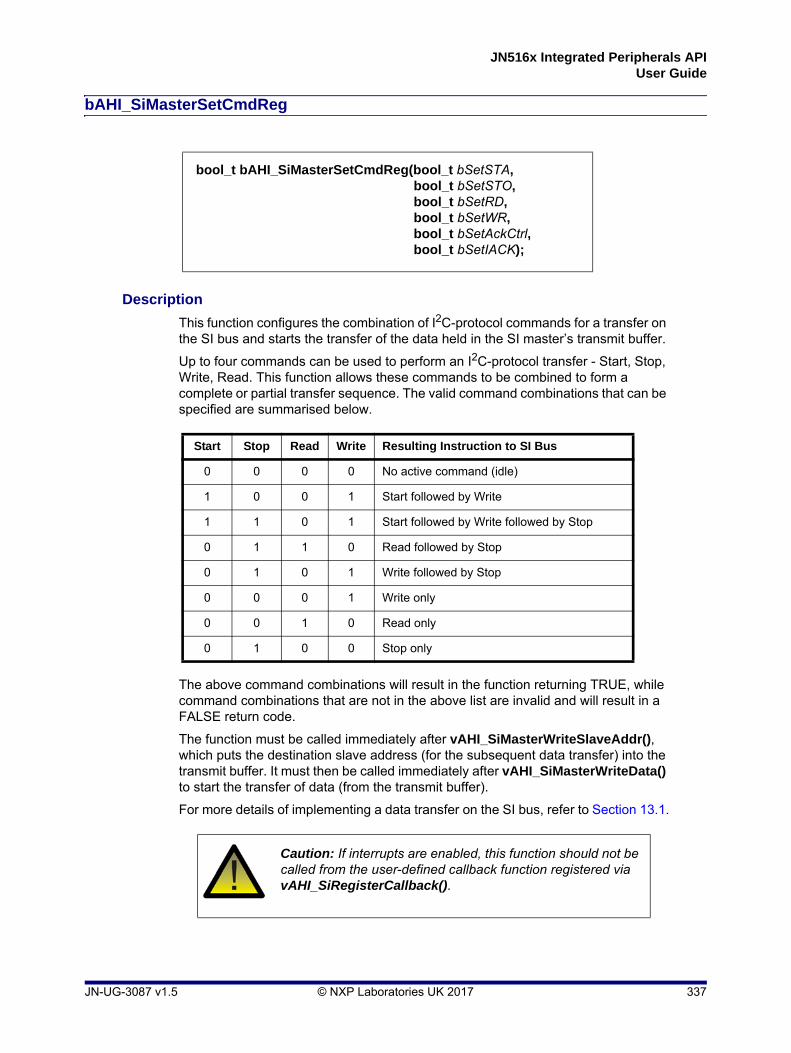
JN516x Integrated Peripherals APIUser Guide
bAHI_SiMasterSetCmdReg
Description
This function configures the combination of I2C-protocol commands for a transfer on the SI bus and starts the transfer of the data held in the SI master’s transmit buffer.
Up to four commands can be used to perform an I2C-protocol transfer - Start, Stop, Write, Read. This function allows these commands to be combined to form a complete or partial transfer sequence. The valid command combinations that can be specified are summarised below.
The above command combinations will result in the function returning TRUE, while command combinations that are not in the above list are invalid and will result in a FALSE return code.
The function must be called immediately after vAHI_SiMasterWriteSlaveAddr(), which puts the destination slave address (for the subsequent data transfer) into the transmit buffer. It must then be called immediately after vAHI_SiMasterWriteData() to start the transfer of data (from the transmit buffer).
For more details of implementing a data transfer on the SI bus, refer to Section 13.1.
bool_t bAHI_SiMasterSetCmdReg(bool_t bSetSTA, bool_t bSetSTO, bool_t bSetRD, bool_t bSetWR, bool_t bSetAckCtrl, bool_t bSetIACK);
Start Stop Read Write Resulting Instruction to SI Bus
0 0 0 0 No active command (idle)
1 0 0 1 Start followed by Write
1 1 0 1 Start followed by Write followed by Stop
0 1 1 0 Read followed by Stop
0 1 0 1 Write followed by Stop
0 0 0 1 Write only
0 0 1 0 Read only
0 1 0 0 Stop only
Caution: If interrupts are enabled, this function should not be called from the user-defined callback function registered via vAHI_SiRegisterCallback().
JN-UG-3087 v1.5 © NXP Laboratories UK 2017 337
Chapter 29Serial Interface (2-wire) Functions
Parameters
bSetSTA Generate START bit to gain control of the SI bus (must not be enabled with STOP bit):E_AHI_SI_START_BIT E_AHI_SI_NO_START_BIT
bSetSTO Generate STOP bit to release control of the SI bus (must not be enabled with START bit):E_AHI_SI_STOP_BIT E_AHI_SI_NO_STOP_BIT
bSetRD Read from slave (cannot be enabled with slave write):E_AHI_SI_SLAVE_READ E_AHI_SI_NO_SLAVE_READ
bSetWR Write to slave (cannot be enabled with slave read):E_AHI_SI_SLAVE_WRITE E_AHI_SI_NO_SLAVE_WRITE
bSetAckCtrl Send ACK or NACK to slave after each byte read:E_AHI_SI_SEND_ACK (to indicate ready for next byte)E_AHI_SI_SEND_NACK (to indicate no more data required)
bSetIACK Generate interrupt acknowledge (should not normally be required as interrupt is cleared by the interrupt handler): E_AHI_SI_IRQ_ACKE_AHI_SI_NO_IRQ_ACK (normally the required setting)
Returns
TRUE if specified command combination is legalFALSE if specified command combination is illegal (will result in no action by device)
Note: This function replaces vAHI_SiMasterSetCmdReg(), which returns no value. However, the previous function is still available in the API for backward compatibility.
338 © NXP Laboratories UK 2017 JN-UG-3087 v1.5

JN516x Integrated Peripherals APIUser Guide
vAHI_SiMasterWriteSlaveAddr
Description
This function is used in setting up communication with a slave device. In this function, you must specify the address of the slave (see below) and the operation (read or write) to be performed on the slave. The function puts this information in the SI master’s transmit buffer, but the information will be not transmitted on the SI bus until the function bAHI_SiMasterSetCmdReg() is called.
A slave address can be 7-bit or 10-bit, where this address size is set using the function vAHI_SiSlaveConfigure() called on the slave device. vAHI_SiMasterWriteSlaveAddr() is used differently for the two slave addressing modes:
For 7-bit addressing, the parameter u8SlaveAddress must be set to the 7-bit slave address.
For 10-bit addressing, the parameter u8SlaveAddress must be set to the binary value 011110xx, where xx are the 2 most significant bits of the 10-bit slave address - the code 011110 indicates to the SI bus slaves that 10-bit addressing will be used in the next communication. The remaining 8 bits of the slave address must subsequently be specified in a call to vAHI_SiMasterWriteData8().
For more details of implementing a data transfer on the SI bus, refer to Section 13.1.
Parameters
u8SlaveAddress Slave address (see above)
bReadStatus Operation to perform on slave (read or write):TRUE - configure a readFALSE - configure a write
Returns
None
void vAHI_SiMasterWriteSlaveAddr(uint8 u8SlaveAddress,bool_t bReadStatus);
JN-UG-3087 v1.5 © NXP Laboratories UK 2017 339

Chapter 29Serial Interface (2-wire) Functions
vAHI_SiMasterWriteData8
Description
This function writes a single data-byte to the transmit buffer of the SI master.
The contents of the transmit buffer will not be transmitted on the SI bus until the function bAHI_SiMasterSetCmdReg() is called.
Parameters
u8Out 8 bits of data to transmit
Returns
None
void vAHI_SiMasterWriteData8(uint8 u8Out);
340 © NXP Laboratories UK 2017 JN-UG-3087 v1.5

JN516x Integrated Peripherals APIUser Guide
u8AHI_SiMasterReadData8
Description
This function obtains a data-byte received over the SI bus.
Parameters
None
Returns
Data read from receive buffer of SI master
uint8 u8AHI_SiMasterReadData8(void);
JN-UG-3087 v1.5 © NXP Laboratories UK 2017 341
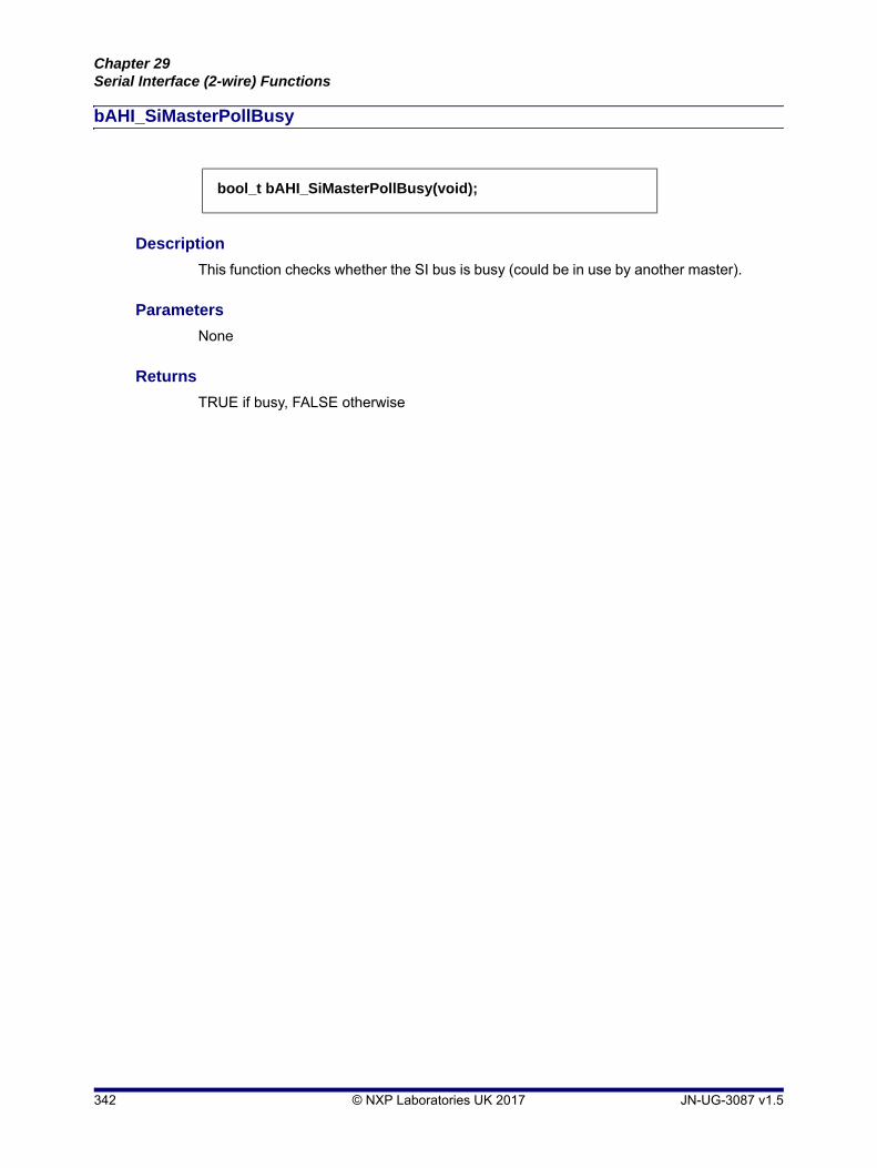
Chapter 29Serial Interface (2-wire) Functions
bAHI_SiMasterPollBusy
Description
This function checks whether the SI bus is busy (could be in use by another master).
Parameters
None
Returns
TRUE if busy, FALSE otherwise
bool_t bAHI_SiMasterPollBusy(void);
342 © NXP Laboratories UK 2017 JN-UG-3087 v1.5

JN516x Integrated Peripherals APIUser Guide
bAHI_SiMasterPollTransferInProgress
Description
This function checks whether a transfer is in progress on the SI bus.
Parameters
None
Returns
TRUE if a transfer is in progress, FALSE otherwise
bool_t bAHI_SiMasterPollTransferInProgress(void);
JN-UG-3087 v1.5 © NXP Laboratories UK 2017 343

Chapter 29Serial Interface (2-wire) Functions
bAHI_SiMasterCheckRxNack
Description
This function checks whether a NACK or an ACK has been received from the slave device. If a NACK has been received, this indicates that the SI master should stop sending data to the slave.
Parameters
None
Returns
TRUE if NACK has occurred
FALSE if ACK has occurred
bool_t bAHI_SiMasterCheckRxNack(void);
344 © NXP Laboratories UK 2017 JN-UG-3087 v1.5
JN516x Integrated Peripherals APIUser Guide
bAHI_SiMasterPollArbitrationLost
Description
This function checks whether arbitration has been lost (by the local master) on the SI bus.
Parameters
None
Returns
TRUE if arbitration loss has occurred, FALSE otherwise
bool_t bAHI_SiMasterPollArbitrationLost(void);
JN-UG-3087 v1.5 © NXP Laboratories UK 2017 345

Chapter 29Serial Interface (2-wire) Functions
29.2 SI Slave Functions
This section details the functions for controlling a 2-wire Serial Interface (SI) slave on the JN516x microcontroller.
As in the case of an SI master, the SI slave uses DIO14 as a clock and DIO15 as a bi-directional data line (but does not supply the clock). These signals can be moved to DIO16 and DIO17, respectively.
The SI Slave functions are listed below, along with their page references:
Function Page
vAHI_SiSlaveConfigure 347
vAHI_SiSlaveDisable 349
vAHI_SiSlaveWriteData8 350
u8AHI_SiSlaveReadData8 351
vAHI_SiSlaveAddressMask (JN5169 Only) 352
vAHI_SiSlaveWriteSlaveSecondryAddr (JN5169 Only) 353
eAHI_SiSlaveAddressStatus (JN5169 Only) 354
bAHI_SiSlavePollBusy (JN5169 Only) 355
346 © NXP Laboratories UK 2017 JN-UG-3087 v1.5
JN516x Integrated Peripherals APIUser Guide
vAHI_SiSlaveConfigure
Description
This function is used to configure and enable the 2-wire Serial Interface (SI) slave. This function must be called before any other SI Slave function. To later disable the interface, the function vAHI_SiSlaveDisable() must be used.
You must specify the address of the slave to be configured and enabled. A 7-bit or 10-bit slave address can be used. The address size must also be specified through bExtendAddr.
The function allows SI slave interrupts to be enabled on an individual basis using an 8-bit bitmask specified through u8InMaskEnable. The SI slave interrupts are enumerated as follows:
To obtain the bitmask for u8InMaskEnable, the enumerations for the interrupts to be enabled can be bitwise ORed together.
A pulse suppression filter can be enabled to suppress any spurious pulses (high or low) with a pulse width less than 62.5ns on the clock and data lines.
Parameters
u16SlaveAddress Slave address (7-bit or 10-bit, as defined by bExtendAdd)
bExtendAddr Size of slave address (specified through u16SlaveAddress):TRUE - 10-bit addressFALSE - 7-bit address
void vAHI_SiSlaveConfigure(uint16 u16SlaveAddress,bool_t bExtendAddr,bool_t bPulseSuppressionEnable,uint8 u8InMaskEnable,bool_t bFlowCtrlMode);
Bit Enumeration Interrupt Description
0 E_AHI_SIS_DATA_RR_MASK Data buffer must be written with data to be read by SI master
1 E_AHI_SIS_DATA_RTKN_MASK Data taken from buffer by SI master - buffer free for next data
2 E_AHI_SIS_DATA_WA_MASK Data buffer contains data from SI master to be read by SI slave
3 E_AHI_SIS_LAST_DATA_MASK Last data transferred (end of burst)
4 E_AHI_SIS_ERROR_MASK I2C protocol error
JN-UG-3087 v1.5 © NXP Laboratories UK 2017 347

Chapter 29Serial Interface (2-wire) Functions
bPulseSuppressionEnable Enable/disable pulse suppression filter:TRUE - enableFALSE - disable
u8InMaskEnable Bitmask of SI slave interrupts to be enabled (see above)
bFlowCtrlMode Flow control mode:TRUE - not valid (reserved for future use)FALSE - NACK (default)
Returns
None
348 © NXP Laboratories UK 2017 JN-UG-3087 v1.5

JN516x Integrated Peripherals APIUser Guide
vAHI_SiSlaveDisable
Description
This function disables (and powers down) the SI slave, if it has been previously enabled using the function vAHI_SiSlaveConfigure().
Parameters
None
Returns
None
void vAHI_SiSlaveDisable(void);
JN-UG-3087 v1.5 © NXP Laboratories UK 2017 349
Chapter 29Serial Interface (2-wire) Functions
vAHI_SiSlaveWriteData8
Description
This function writes a single byte of output data to the data buffer of the SI slave, ready to be read by the SI master.
Parameters
u8Out 8 bits of output data
Returns
None
void vAHI_SiSlaveWriteData8(uint8 u8Out);
350 © NXP Laboratories UK 2017 JN-UG-3087 v1.5
JN516x Integrated Peripherals APIUser Guide
u8AHI_SiSlaveReadData8
Description
This function reads a single byte of input data from the buffer of the SI slave (where this data byte has been received from the SI master).
Parameters
None
Returns
Input data-byte read from buffer of SI slave
uint8 u8AHI_SiSlaveReadData8(void);
JN-UG-3087 v1.5 © NXP Laboratories UK 2017 351

Chapter 29Serial Interface (2-wire) Functions
vAHI_SiSlaveAddressMask (JN5169 Only)
Description
This function can be used on the JN5169 device to specify the methods that can be employed to address the SI Slave. Normally, the interface would be addressed using its primary address, but it can also be addressed by one or both of the following methods:
Secondary address: This is an alternative 7-bit address which must (first) be specified using the function vAHI_SiSlaveWriteSlaveSecondryAddr()
General call: This is a broadcast for which the address is zero
Thus, any combination of the above addresses can be enabled in this function and the interface will then accept communications made to those addresses.
Parameters
bGeneralCall Boolean value which enables (TRUE) or disables (FALSE) use of ‘general calls’ (broadcasts)
bSecondaryAddress Boolean value which enables (TRUE) or disables (FALSE) use of a secondary address
bPrimaryAddress Boolean value which enables (TRUE) or disables (FALSE) use of a primary address
Returns
None
void vAHI_SiSlaveAddressMask(bool_t bGeneralCall,bool_t bSecondaryAddress,bool_t bPrimaryAddress);
352 © NXP Laboratories UK 2017 JN-UG-3087 v1.5
JN516x Integrated Peripherals APIUser Guide
vAHI_SiSlaveWriteSlaveSecondryAddr (JN5169 Only)
Description
This function can be used on a JN5169 device to specify a secondary address for the SI Slave. This is a 7-bit address and the most significant bit (bit 7) of the specified uint8 value must be set to ‘0’.
If required, use of the secondary address must subsequently be enabled through a call to the functon vAHI_SiSlaveAddressMask().
Parameters
u8SlaveSecondaryAddress 7-bit secondary address to use (set bit 7 to ‘0’)
Returns
None
void vAHI_SiSlaveWriteSlaveSecondryAddr(uint8 u8SlaveSecondaryAddress);
JN-UG-3087 v1.5 © NXP Laboratories UK 2017 353

Chapter 29Serial Interface (2-wire) Functions
eAHI_SiSlaveAddressStatus (JN5169 Only)
Description
This function can be used on a JN5169 device to obtain the status of the SI Slave access that is currently in progress. The return code indicates both the access type (read or write) and the addressing method used for the access (primary address, secondary address, general call):
Write using primary address
Write using secondary address
Write as a general call (broadcast)
Read using primary address
Read using secondary address
Parameters
None
Returns
SIS_ADDR_STATUS_PRIMARY_WR_TRANSFER (0)
SIS_ADDR_STATUS_SECONDARY_WR_TRANSFER (2)
SIS_ADDR_STATUS_GENERAL_CALL_WR_TRANSFER (4)
SIS_ADDR_STATUS_PRIMARY_RD_TRANSFER (8)
SIS_ADDR_STATUS_SECONDARY_RD_TRANSFER (16)
teSISAddrStatus eAHI_SiSlaveAddressStatus(void);
354 © NXP Laboratories UK 2017 JN-UG-3087 v1.5
JN516x Integrated Peripherals APIUser Guide
bAHI_SiSlavePollBusy (JN5169 Only)
Description
This function can be used on a JN5169 device to poll the ‘Busy’ flag of the SI Slave to determine whether a data transfer to or from the interface is in progress.
Parameters
None
Returns
TRUE (data transfer in progress) or FALSE (data transfer not in progress)
bool_t bAHI_SiSlavePollBusy(void);
JN-UG-3087 v1.5 © NXP Laboratories UK 2017 355

Chapter 29Serial Interface (2-wire) Functions
29.3 General SI Functions
This section describes the General SI functions that can be used for both an SI master and SI slave on the JN516x microcontroller.
The functions are listed below, along with their page references:
Function Page
vAHI_SiSetLocation 357
vAHI_SiRegisterCallback 358
356 © NXP Laboratories UK 2017 JN-UG-3087 v1.5
JN516x Integrated Peripherals APIUser Guide
vAHI_SiSetLocation
Description
This function can be used to select the pair of DIOs on which the Serial Interface (SI) will operate: either DIO14-15 or DIO16-17. By default, DIO14-15 are used, so the function only needs to be called if DIO16-17 are preferred.
The function can be used on an SI master or an SI slave.
Parameters
bLocation DIOs on which interface will operate:TRUE - DIO16-17FALSE - DIO14-15 (default)
Returns
None
void vAHI_SiSetLocation(bool_t bLocation);
JN-UG-3087 v1.5 © NXP Laboratories UK 2017 357

Chapter 29Serial Interface (2-wire) Functions
vAHI_SiRegisterCallback
Description
This function registers a user-defined callback function that will be called when a Serial Interface interrupt is triggered on an SI master or on an SI slave.
Note that this function can be used to register the callback function for the SI master or for a SI slave, but both callback functions cannot exist in the application at the same time.
The registered callback function is only preserved during sleep modes in which RAM remains powered. If RAM is powered off during sleep and interrupts are required, the callback function must be re-registered before calling u32AHI_Init() on waking.
Interrupt handling is described in Appendix A.
Parameters
prSiCallback Pointer to callback function to be registered
Returns
None
void vAHI_SiRegisterCallback(PR_HWINT_APPCALLBACK prSiCallback);
358 © NXP Laboratories UK 2017 JN-UG-3087 v1.5

JN516x Integrated Peripherals APIUser Guide
30. SPI Master Functions
This chapter details the functions for controlling the Serial Peripheral Interface (SPI) master on the JN516x microcontroller. The SPI allows high-speed synchronous data transfer between the microcontroller and peripheral devices. When JN516x device operates as the master on the SPI bus, all other devices connected to the bus are expected to be slave devices under the control of the microcontroller’s CPU.
The SPI Master functions are listed below, along with their page references:
Function Page
vAHI_SpiConfigure 360
vAHI_SpiReadConfiguration 362
vAHI_SpiRestoreConfiguration 363
vAHI_SpiSelSetLocation 364
vAHI_SpiSelect 365
vAHI_SpiStop 366
vAHI_SpiDisable 367
vAHI_SpiStartTransfer 368
u32AHI_SpiReadTransfer32 369
u16AHI_SpiReadTransfer16 370
u8AHI_SpiReadTransfer8 371
vAHI_SpiContinuous 372
bAHI_SpiPollBusy 373
vAHI_SpiWaitBusy 374
vAHI_SetDelayReadEdge 375
vAHI_SpiRegisterCallback 376
Note 1: For information on the SPI master and guidance on using the SPI Master functions in JN516x application code, refer to Chapter 14.
Note 2: SPI Slave functions are detailed in Chapter 31.
Note 3: On a JN516x device, the SPI Master is disabled by default and shares its pins with other functions - this is unlike a JN514x device that uses dedicated pins for the SPI Master, which is enabled from reset in order to boot from an external Flash device.
JN-UG-3087 v1.5 © NXP Laboratories UK 2017 359

Chapter 30SPI Master Functions
vAHI_SpiConfigure
Description
This function configures and enables the SPI master.
The function allows the number of SPI slaves (of the master) to be set. Up to three slave-select lines can be set, which use DIO19, DIO0 and DIO1 (but the last two lines can be moved to DIO14 and DIO15, respectively). Note that once reserved for SPI use, DIO lines cannot be subsequently released by calling this function again (and specifying a smaller number of SPI slaves).
The following features are also configurable using this function:
Data transfer order - whether the least significant bit is transferred first or last
Clock polarity and phase, which together determine the SPI mode (0, 1, 2 or 3) and therefore the clock edge on which data is latched:
SPI Mode 0: polarity=0, phase=0
SPI Mode 1: polarity=0, phase=1
SPI Mode 2: polarity=1, phase=0
SPI Mode 3: polarity=1, phase=1
Clock divisor - the value used to derive the SPI clock from the peripheral clock
SPI interrupt - generated when an API transfer has completed (note that interrupts are only worth using if the SPI clock frequency is much less than 16MHz)
Automatic slave selection - enable the programmed slave-select line or lines (see vAHI_SpiSelect()) to be automatically asserted at the start of a transfer and de-asserted when the transfer completes. If not enabled, the slave-select lines will reflect the value set by vAHI_SpiSelect() directly.
Parameters
u8SlaveEnable Number of SPI slaves to control. Valid values are 0-3 (higher values are truncated to 3)
bLsbFirst Enable/disable data transfer with the least significant bit (LSB) transferred first:TRUE - enableFALSE - disable
bPolarity Clock polarity:FALSE - unchangedTRUE - inverted
void vAHI_SpiConfigure(uint8 u8SlaveEnable, bool_t bLsbFirst, bool_t bPolarity, bool_t bPhase, uint8 u8ClockDivider, bool_t bInterruptEnable, bool_t bAutoSlaveSelect);
360 © NXP Laboratories UK 2017 JN-UG-3087 v1.5

JN516x Integrated Peripherals APIUser Guide
bPhase Phase: FALSE - latch data on leading edge of clockTRUE - latch data on trailing edge of clock
u8ClockDivider Clock divisor in the range 0 to 63. Peripheral clock is divided by 2 x u8ClockDivider, but 0 is a special value used when no clock division is required
bInterruptEnable Enable/disable interrupt when an SPI transfer has completed:TRUE - enableFALSE - disable
bAutoSlaveSelect Enable/disable automatic slave selection:TRUE - enableFALSE - disable
Note that the parameters bPolarity and bPhase are named differently in the library header file.
Returns
None
JN-UG-3087 v1.5 © NXP Laboratories UK 2017 361
Chapter 30SPI Master Functions
vAHI_SpiReadConfiguration
Description
This function obtains the current configuration of the SPI bus.
This function is intended to be used in a system where the SPI bus is used in multiple configurations to allow the state to be restored later using the function vAHI_SpiRestoreConfiguration(). Therefore, no knowledge is needed of the configuration details.
Parameters
*ptConfiguration Pointer to location to receive obtained SPI configuration
Returns
None
void vAHI_SpiReadConfiguration( tSpiConfiguration *ptConfiguration);
362 © NXP Laboratories UK 2017 JN-UG-3087 v1.5

JN516x Integrated Peripherals APIUser Guide
vAHI_SpiRestoreConfiguration
Description
This function restores the SPI bus configuration using the configuration previously obtained using vAHI_SpiReadConfiguration().
Parameters
*ptConfiguration Pointer to SPI configuration to be restored
Returns
None
void vAHI_SpiRestoreConfiguration(tSpiConfiguration *ptConfiguration);
JN-UG-3087 v1.5 © NXP Laboratories UK 2017 363

Chapter 30SPI Master Functions
vAHI_SpiSelSetLocation
Description
This function can be used to select the DIO on which the specified SPI slave select line will operate. The DIO for slave select line SPISEL1 or SPISEL2 can be configured using this function:
SPISEL1 can use DIO0 (default) or alternatively DIO14
SPISEL2 can use DIO1 (default) or alternatively DIO15
The function only needs to be called if the alternative DIO is preferred.
Parameters
u8SpiSel Slave select line to be configured:E_AHI_SPISEL_1 - Slave select 1E_AHI_SPISEL_2 - Slave select 2
bLocation DIO on which specified slave select line will operate:TRUE - DIO14 (SPISEL1) or DIO15 (SPISEL2)FALSE - DIO0 (SPISEL1) or DIO1 (SPISEL2)
Returns
None
void vAHI_SpiSelSetLocation(uint8 u8SpiSel, bool_t bLocation);
364 © NXP Laboratories UK 2017 JN-UG-3087 v1.5
JN516x Integrated Peripherals APIUser Guide
vAHI_SpiSelect
Description
This function sets the active slave-select line(s) to use.
The slave-select lines are asserted immediately if “automatic slave selection” is disabled, or otherwise only during data transfers. The number of valid bits in u8SlaveMask depends on the setting of u8SlaveEnable in a previous call to vAHI_SpiConfigure(), as follows:
Parameters
u8SlaveMask Bitmap - one bit per slave-select line
Returns
None
void vAHI_SpiSelect(uint8 u8SlaveMask);
u8SlaveEnable Valid bits in u8SlaveMask
0 Bit 0
1 Bits 0, 1
2 Bits 0, 1, 2
3 Bits 0, 1, 2, 3
4 Bits 0, 1, 2, 3, 4
JN-UG-3087 v1.5 © NXP Laboratories UK 2017 365

Chapter 30SPI Master Functions
vAHI_SpiStop
Description
This function clears any active slave-select lines. It has the same effect as vAHI_SpiSelect(0).
Parameters
None
Returns
None
void vAHI_SpiStop(void);
366 © NXP Laboratories UK 2017 JN-UG-3087 v1.5

JN516x Integrated Peripherals APIUser Guide
vAHI_SpiDisable
Description
This function disables the SPI Master.
Parameters
None
Returns
None
void vAHI_SpiDisable(void);
JN-UG-3087 v1.5 © NXP Laboratories UK 2017 367
Chapter 30SPI Master Functions
vAHI_SpiStartTransfer
Description
This function can be used to start a data transfer to selected slave(s). The data length for the transfer can be specified in the range 1 to 32 bits.
It is assumed that vAHI_SpiSelect() has been called to set the slave(s) to communicate with. If interrupts are enabled for the SPI master, an interrupt will be generated when the transfer has completed.
The function u32AHI_SpiReadTransfer32() should be used to read the transferred data, with the data aligned to the right (lower bits).
Parameters
u8CharLen Value in range 0-31 indicating data length for transfer:0 - 1-bit data1 - 2-bit data2 - 3-bit data: 31 - 32-bit data
u32Out Data to transmit, aligned to the right(e.g. for an 8-bit transfer, store the data in bits 0-7)
Returns
None
void vAHI_SpiStartTransfer(uint8 u8CharLen, uint32 u32Out);
368 © NXP Laboratories UK 2017 JN-UG-3087 v1.5

JN516x Integrated Peripherals APIUser Guide
u32AHI_SpiReadTransfer32
Description
This function obtains the received data after a SPI transfer has completed that was started using vAHI_SpiStartTransfer() or vAHI_SpiSetContinuous(). The read data is aligned to the right (lower bits).
Parameters
None
Returns
Received data (32 bits)
uint32 u32AHI_SpiReadTransfer32(void);
JN-UG-3087 v1.5 © NXP Laboratories UK 2017 369

Chapter 30SPI Master Functions
u16AHI_SpiReadTransfer16
Description
This function obtains the received data after a 16-bit SPI transfer has completed.
Parameters
None
Returns
Received data (16 bits)
uint16 u16AHI_SpiReadTransfer16(void);
370 © NXP Laboratories UK 2017 JN-UG-3087 v1.5

JN516x Integrated Peripherals APIUser Guide
u8AHI_SpiReadTransfer8
Description
This function obtains the received data after a 8-bit SPI transfer has completed.
Parameters
None
Returns
Received data (8 bits)
uint8 u8AHI_SpiReadTransfer8(void);
JN-UG-3087 v1.5 © NXP Laboratories UK 2017 371

Chapter 30SPI Master Functions
vAHI_SpiContinuous
Description
This function can be used to enable/disable continuous read mode. The function allows continuous data transfers to the SPI master and facilitates back-to-back reads of the received data. In this mode, incoming data transfers are automatically controlled by hardware - data is received and the hardware then waits for this data to be read by the software before allowing the next data transfer.
The data length for an individual transfer can be specified in the range 1 to 32 bits.
If used to enable continuous mode, the function will start the transfers (so there is no need to call a SPI start transfer function. If used to disable continuous mode, the function will stop any existing transfers (following the function call, one more transfer is made before the transfers are stopped).
To determine when data is ready to be read, the application should check whether the interface is busy by calling the function bAHI_SpiPollBusy(). If it is not busy receiving data, the data from the previous transfer can be read by calling u32AHI_SpiReadTransfer32(), with the data aligned to the right (lower bits). Once the data has been read, the next transfer will automatically occur.
Parameters
bEnable Enable/disable continuous read mode and start/stop transfers:TRUE - enable mode and start transfersFALSE - stop transfers and disable mode
u8CharLen Value in range 0-31 indicating data length for transfer:0 - 1-bit data1 - 2-bit data2 - 3-bit data: 31 - 32-bit data
Returns
None
void vAHI_SpiContinuous(bool_t bEnable, uint8 u8CharLen);
372 © NXP Laboratories UK 2017 JN-UG-3087 v1.5
JN516x Integrated Peripherals APIUser Guide
bAHI_SpiPollBusy
Description
This function polls the SPI master to determine whether it is currently busy performing a data transfer.
Parameters
None
Returns
TRUE if the SPI master is performing a transfer, FALSE otherwise
bool_t bAHI_SpiPollBusy(void);
JN-UG-3087 v1.5 © NXP Laboratories UK 2017 373

Chapter 30SPI Master Functions
vAHI_SpiWaitBusy
Description
This function waits for the SPI master to complete a transfer and then returns.
Parameters
None
Returns
None
void vAHI_SpiWaitBusy(void);
374 © NXP Laboratories UK 2017 JN-UG-3087 v1.5

JN516x Integrated Peripherals APIUser Guide
vAHI_SetDelayReadEdge
Description
This function can be used to introduce a delay to the SCLK edge used to sample received data. The delay is by half a SCLK period relative to the normal position (so is the same edge used by the slave device to transmit the next data bit).
The function should be used when the round-trip delay of SCLK out to MISO IN is large compared with half a SCLK period (e.g. fast SCLK, low voltage, slow slave device), to allow a faster transfer rate to be used than would otherwise be possible.
Parameters
bSetDreBit Enable/disable read edge delay:TRUE - enableFALSE - disable
Returns
None
void vAHI_SpiSetDelayReadEdge(bool_t bSetDreBit);
JN-UG-3087 v1.5 © NXP Laboratories UK 2017 375
Chapter 30SPI Master Functions
vAHI_SpiRegisterCallback
Description
This function registers an application callback that will be called when the SPI interrupt is triggered.
The registered callback function is only preserved during sleep modes in which RAM remains powered. If RAM is powered off during sleep and interrupts are required, the callback function must be re-registered before calling u32AHI_Init() on waking.
Interrupt handling is described in Appendix A.
Parameters
prSpiCallback Pointer to callback function to be registered
Returns
None
void vAHI_SpiRegisterCallback(PR_HWINT_APPCALLBACK prSpiCallback);
376 © NXP Laboratories UK 2017 JN-UG-3087 v1.5

JN516x Integrated Peripherals APIUser Guide
31. SPI Slave Functions
This chapter details the functions for controlling the Serial Peripheral Interface (SPI) slave on the JN516x microcontroller.
The SPI Slave functions are listed below, along with their page references:
Function Page
bAHI_SpiSlaveEnable 378
vAHI_SpiSlaveDisable 379
vAHI_SpiSlaveReset 380
vAHI_SpiSlaveTxWriteByte 381
u8AHI_SpiSlaveRxReadByte 382
u8AHI_SpiSlaveTxFillLevel 383
u8AHI_SpiSlaveRxFillLevel 384
u8AHI_SpiSlaveStatus 385
vAHI_SpiSlaveRegisterCallback 386
Note 1: For information on the SPI slave and guidance on using the SPI Slave functions in JN516x application code, refer to Chapter 15.
Note 2: SPI Master functions are detailed in Chapter 30.
Note 3: For more details of the data message format, refer to the data sheet for your microcontroller.
JN-UG-3087 v1.5 © NXP Laboratories UK 2017 377

Chapter 31SPI Slave Functions
bAHI_SpiSlaveEnable
Description
This function initialises and configures the SPI Slave.
Parameters
bPinLocation Configures pin location of SPISMISO and SPISMOSI:TRUE - SPISMISO : DIO17, SPISMOSI : DIO16FALSE - SPISMISO : DIO13, SPISMOSI : DIO12
bLsbFirst Configures serial bit-order:TRUE - SPI data byte transferred LSB firstFALSE - SPI data byte transferred MSB first
*pu8TxBuffer Pointer to start of Transmit buffer in RAM
u8TxBufferLength Length of Transmit buffer, in bytes (1 to 255)
u8TxBufferThreshold Fill threshold of Transmit buffer, in bytes (0 to 255)
*pu8RxBuffer Pointer to start of Receive buffer in RAM
u8RxBufferLength Length of Receive buffer, in bytes (1 to 255)
u8RxBufferThreshold Fill threshold of Receive buffer, in bytes (0 to 255)
u16RxTimeOut Receive timeout duration, in microseconds (0 to 4095)
u16InterruptEnableMask Interrupt enable mask (bit): †E_AHI_SPIS_INT_RX_FIRST_MASK (0)E_AHI_SPIS_INT_TX_LAST_MASK (1)E_AHI_SPIS_INT_RX_CLIMB_MASK (2)E_AHI_SPIS_INT_TX_FALL_MASK (3)E_AHI_SPIS_INT_RX_OVER_MASK (4)E_AHI_SPIS_INT_TX_OVER_MASK (5)E_AHI_SPIS_INT_RX_UNDER_MASK (6)E_AHI_SPIS_INT_TX_UNDER_MASK (7)E_AHI_SPIS_INT_RX_TIMEOUT_MASK (8)
† Refer to Table 17 in Appendix B.2 for a description of each mask bit enumeration.
Returns
TRUE if successfully configured, FALSE otherwise (i.e. invalid input parameters)
bool_t bAHI_SpiSlaveEnable(bool_t bPinLocation,bool_t bLsbFirst,uint8 *pu8TxBuffer,uint8 u8TxBufferLength,uint8 u8TxBufferThreshold,uint8 *pu8RxBuffer,uint8 u8RxBufferLength,uint8 u8RxBufferThreshold,uint16 u16RxTimeOut,uint16 u16InterruptEnableMask);
378 © NXP Laboratories UK 2017 JN-UG-3087 v1.5
JN516x Integrated Peripherals APIUser Guide
vAHI_SpiSlaveDisable
Description
This function can be used to disable the SPI Slave.
Parameters
None
Returns
None
void vAHI_SpiSlaveDisable(void);
JN-UG-3087 v1.5 © NXP Laboratories UK 2017 379
Chapter 31SPI Slave Functions
vAHI_SpiSlaveReset
Description
This function can be used to reset the Transmit and/or Receive FIFO buffers. Following a reset, the internal buffer pointers are re-initialised, the fill-level is reset to zero and the buffer contents remain unchanged.
Parameters
bTxReset Transmit buffer reset:TRUE - Reset bufferFALSE - Do not reset buffer
bRxReset Receive buffer reset:TRUE - Reset bufferFALSE - Do not reset buffer
Returns
None
void vAHI_SpiSlaveReset(bool_t bTxReset,bool_t bRxReset);
380 © NXP Laboratories UK 2017 JN-UG-3087 v1.5

JN516x Integrated Peripherals APIUser Guide
vAHI_SpiSlaveTxWriteByte
Description
This function writes a byte of data to the Transmit FIFO buffer of the SPI Slave.
Parameters
u8Byte Data byte to write to the Transmit FIFO buffer
Returns
None
void vAHI_SpiSlaveTxWriteByte(uint8 u8Byte);
JN-UG-3087 v1.5 © NXP Laboratories UK 2017 381

Chapter 31SPI Slave Functions
u8AHI_SpiSlaveRxReadByte
Description
This function reads a byte of data from the Receive FIFO of the SPI Slave.
Parameters
None
Returns
Data byte read from the Receive FIFO buffer
uint8 u8AHI_SpiSlaveRxReadByte(void);
382 © NXP Laboratories UK 2017 JN-UG-3087 v1.5
JN516x Integrated Peripherals APIUser Guide
u8AHI_SpiSlaveTxFillLevel
Description
This function returns the fill-level of the Transmit FIFO buffer of the SPI Slave.
Parameters
None
Returns
Fill-level of Transmit FIFO buffer
uint8 u8AHI_SpiSlaveTxFillLevel(void);
JN-UG-3087 v1.5 © NXP Laboratories UK 2017 383
Chapter 31SPI Slave Functions
u8AHI_SpiSlaveRxFillLevel
Description
This function returns the fill-level of the Receive FIFO buffer of the SPI Slave.
Parameters
None
Returns
Fill-level of Receive FIFO buffer
uint8 u8AHI_SpiSlaveRxFillLevel(void);
384 © NXP Laboratories UK 2017 JN-UG-3087 v1.5

JN516x Integrated Peripherals APIUser Guide
u8AHI_SpiSlaveStatus
Description
This function returns a bitmap indicating the status of the SPI Slave.
Parameters
None
Returns
SPI Slave status bitmap which can be bitwise ANDed with the following masks:
E_AHI_SPIS_STAT_RX_AVAIL_MASK (0x1) Receive buffer not empty
E_AHI_SPIS_STAT_TX_PENDING_MASK (0x2) Transmit buffer not empty
E_AHI_SPIS_STAT_RX_ABOVE_MASK (0x4) Receive buffer fill-level abovethreshold
E_AHI_SPIS_STAT_TX_ABOVE_MASK (0x8) Transmit buffer fill-level abovethreshold
uint8 u8AHI_SpiSlaveStatus(void);
JN-UG-3087 v1.5 © NXP Laboratories UK 2017 385

Chapter 31SPI Slave Functions
vAHI_SpiSlaveRegisterCallback
Description
This function registers an application callback that will be called when the SPI Slave interrupt is triggered.
The registered callback function is only preserved during sleep modes in which RAM remains powered. If RAM is powered off during sleep and interrupts are required, the callback function must be re-registered before calling u32AHI_Init() on waking.
Interrupt handling is described in Appendix A.
Parameters
prSpiCallback Pointer to callback function to be registered
Returns
None
void vAHI_SpiSlaveRegisterCallback(PR_HWINT_APPCALLBACK prSpiCallback);
386 © NXP Laboratories UK 2017 JN-UG-3087 v1.5

JN516x Integrated Peripherals APIUser Guide
32. Flash Memory Functions
This chapter describes functions for erasing and programming a sector of a Flash memory device. The Flash memory can be the on-chip device or an external device.
Functions are supplied that can be used to interact with any compatible Flash device (detailed in Section 16.1). They are able to access any sector of Flash memory - the application is stored from the first sector (0) and application data is normally stored in the final sector.
The Flash Memory functions are listed below, along with their page references:
Function Page
bAHI_FlashInit 388
bAHI_FlashEraseSector 390
bAHI_FullFlashProgram 391
bAHI_FullFlashRead 392
vAHI_FlashPowerDown 393
vAHI_FlashPowerUp 394
bAHI_FlashEECerrorInterruptSet 395
vAHI_ExtendedTemperatureOperation 396
Note 1: To access sectors other than the final sector, you should refer to the data sheet for the Flash device to obtain the necessary sector details. However, be careful not to erase essential data such as application code. The application is stored from Sector 0 of the on-chip Flash memory.
Note 2: All Flash addresses specified in these functions are offsets from the start of Flash memory and not absolute addresses.
Note 3: For guidance on using the Flash memory functions in JN516x application code, refer to Chapter 16.
JN-UG-3087 v1.5 © NXP Laboratories UK 2017 387

Chapter 32Flash Memory Functions
bAHI_FlashInit
Description
This function selects the type of Flash memory device to be used.
The Flash memory device can be one of the supported device types or a custom device. In the latter case, a custom table of functions must be supplied for interaction with the device.
For information on the Flash memory devices supported by each JN516x microcontroller, refer to Section 16.1.
Parameters
flashType Type of Flash memory device, one of:E_FL_CHIP_ATMEL_AT25F512 (Atmel AT25F512)E_FL_CHIP_ST_M25P05_A (ST M25P05A)E_FL_CHIP_ST_M25P10_A (ST M25P10A)E_FL_CHIP_ST_M25P20_A (ST M25P20 /
Winbond W25X20B) †E_FL_CHIP_ST_M25P40_A (ST M25P40)E_FL_CHIP_SST_25VF010 (Microchip SST25VF010A) ††E_FL_CHIP_CUSTOM (custom external device)E_FL_CHIP_INTERNAL (on-chip Flash memory)E_FL_CHIP_AUTO (on-chip Flash memory)
*pCustomFncTable Pointer to the function table for a custom Flash device (E_FL_CHIP_CUSTOM) - see below. If a supported Flash device is used, set to NULL.
† The Winbond W25X20B device is similar to the ST M25P20 device and should be specified as the latter (E_FL_CHIP_ST_M25P20_A).
†† The Microchip SST25VF010A device is supported using 4x32KB overlay blocks instead of 32x4KB sectors.
bool_t bAHI_FlashInit(teFlashChipType flashType, tSPIflashFncTable *pCustomFncTable);
Note: If you wish to use both internal (on-chip) and external Flash memory devices, you will need to call bAHI_FlashInit() when switching between them.
388 © NXP Laboratories UK 2017 JN-UG-3087 v1.5

JN516x Integrated Peripherals APIUser Guide
Custom Flash Functions
If a custom Flash memory device is to be used, a set of custom Flash functions (that will be invoked by the supplied Flash functions to access the custom device) must be provided via the following structure pointed to by the pCustomFncTable parameter:
typedef struct tagSPIflashFncTable {
uint32 u32Signature;
uint16 u16FlashId;
uint16 u16Reserved;
tpfvZSPIflashInit vZSPIflashInit;
tpfvZSPIflashSetSlaveSel vZSPIflashSetSlaveSel;
tpfvZSPIflashWREN vZSPIflashWREN;
tpfvZSPIflashEWRSR vZSPIflashEWRSR;
tpfu8ZSPIflashRDSR u8ZSPIflashRDSR;
tpfu16ZSPIflashRDID u16ZSPIflashRDID;
tpfvZSPIflashWRSR vZSPIflashWRSR;
tpfvZSPIflashPP vZSPIflashPP;
tpfvZSPIflashRead vZSPIflashRead;
tpfvZSPIflashBE vZSPIflashBE;
tpfvZSPIflashSE vZSPIflashSE;
} tSPIflashFncTable;
The custom function protypes are listed below:
typedef void (*tpfvZSPIflashInit)(int iDivisor, uint8 u8SlaveSel);
typedef void (*tpfvZSPIflashSetSlaveSel)(uint8 u8SlaveSel);
typedef void (*tpfvZSPIflashWREN)(void);
typedef void (*tpfvZSPIflashEWRSR)(void);
typedef uint8 (*tpfu8ZSPIflashRDSR)(void);
typedef uint16 (*tpfu16ZSPIflashRDID)(void);
typedef void (*tpfvZSPIflashWRSR)(uint8 u8Data);
typedef void (*tpfvZSPIflashPP)(uint32 u32Addr, uint16 u16Len, uint8* pu8Data);
typedef void (*tpfvZSPIflashRead)(uint32 u32Addr, uint16 u16Len, uint8* pu8Data);
typedef void (*tpfvZSPIflashBE)(void);
typedef void (*tpfvZSPIflashSE)(uint8 u8Sector);
Returns
TRUE if initialisation was successful
FALSE if failed
JN-UG-3087 v1.5 © NXP Laboratories UK 2017 389

Chapter 32Flash Memory Functions
bAHI_FlashEraseSector
Description
This function erases the specified sector of Flash memory by setting all bits to 1.
The function can be used with any compatible Flash memory device with up to 8 sectors. Refer to the data sheet of the Flash memory device for details of its sectors.
Parameters
u8Sector Number of the sector to be erased (in the range 0 to 7)
Returns
TRUE if sector erase was successful, FALSE if erase failed
bool_t bAHI_FlashEraseSector(uint8 u8Sector);
Caution: Be careful not to erase essential data such as application code. The application is stored from the start of the on-chip Flash memory (starting in Sector 0).
390 © NXP Laboratories UK 2017 JN-UG-3087 v1.5

JN516x Integrated Peripherals APIUser Guide
bAHI_FullFlashProgram
Description
This function programs a block of Flash memory by clearing the appropriate bits from 1 to 0. The function can be used to access any sector of a compatible Flash memory device. This function must only be used to write a block of data containing a multiple of 16 bytes and this block must be written to a 16-byte boundary.
This mechanism does not allow bits to be set from 0 to 1. It is only possible to set bits to 1 by erasing the entire sector - therefore, before using this function, you must call the function bAHI_FlashEraseSector().
Parameters
u32Addr Address offset from start of Flash memory of first byte to be programmed (must be on a 16-byte boundary)
u16Len Number of bytes to be programmed (must be a multiple of 16 up to 0x8000)
*pu8Data Pointer to start of data block to be written to Flash memory
Returns
TRUE if write was successful
FALSE if write failed
bool_t bAHI_FullFlashProgram(uint32 u32Addr, uint16 u16Len, uint8 *pu8Data);
Caution: Each sector of the internal Flash memory in the JN516x device is divided into 16-byte pagewords. A write to a non-blank pageword must not be performed - the sector containing the non-blank pageword should first be erased using bAHI_FlashEraseSector() before writing to the pageword. If the user omits the sector-erase operation, a subsequent error will likely result when reading from the pageword - this read-error will trigger an interrupt and execute the callback function registered using bAHI_FlashEECerrorInterruptSet().
Caution: The internal Flash memory of the JN516x device has an endurance limit of 10000 write/erase cycles per sector. Refer to the device-specific data sheet for the endurance limit of the external Flash memory.
JN-UG-3087 v1.5 © NXP Laboratories UK 2017 391
Chapter 32Flash Memory Functions
bAHI_FullFlashRead
Description
This function reads data from the application data area of Flash memory. The function can be used to access any sector of a compatible Flash memory device.
If the function parameters are invalid (e.g. by trying to read beyond end of sector), the function returns without reading anything.
Parameters
u32Addr Address offset from start of Flash memory of first byte to be read
u16Len Number of bytes to be read: integer in range 1 to 0x8000
*pu8Data Pointer to start of buffer to receive read data.
Returns
TRUE (always)
bool_t bAHI_FullFlashRead(uint32 u32Addr, uint16 u16Len, uint8 *pu8Data);
392 © NXP Laboratories UK 2017 JN-UG-3087 v1.5

JN516x Integrated Peripherals APIUser Guide
vAHI_FlashPowerDown
Description
This function sends a ‘power down’ command to an external Flash memory device attached to the JN516x device. This allows further power savings to be made when the microcontroller is put into a sleep mode (including Deep Sleep).
The following Flash devices are supported by this function:
STM25P05A
STM25P10A
STM25P20
STM25P40
If the function is called for an unsupported Flash device, the function will return without doing anything.
The application on a JN516x device is responsible for managing the power to external Flash memory for all sleep modes (including Deep Sleep). If the external Flash device is to be unpowered while the JN516x device is sleeping, this function must be called before vAHI_Sleep() is called to put the CPU into Sleep mode. You must subsequently power up the device using vAHI_FlashPowerUp() after waking and before attempting to access the Flash memory.
Parameters
None
Returns
None
void vAHI_FlashPowerDown(void);
Caution: This function must not be called when using the JN516x on-chip Flash memory device - that is, when bAHI_FlashInit() has been called with the Flash device type E_FL_CHIP_INTERNAL or E_FL_CHIP_AUTO specified. Note that when using the JenOS Persistent Data Manager (PDM), the E_FL_CHIP_AUTO option is used by default, in which case the on-chip Flash memory device will be detected.
JN-UG-3087 v1.5 © NXP Laboratories UK 2017 393

Chapter 32Flash Memory Functions
vAHI_FlashPowerUp
Description
This function sends a ‘power up’ command to an external Flash memory device attached to the JN516x device.
The following Flash devices are supported by this function:
STM25P05A
STM25P10A
STM25P20
STM25P40
If the function is called for an unsupported Flash device, the function will return without doing anything.
The application on a JN516x device is responsible for managing the power to external Flash memory for all sleep modes (including Deep Sleep). This function must be called when the JN516x device wakes from sleep if the Flash device was powered down using vAHI_FlashPowerDown() before the device entered Sleep mode.
Parameters
None
Returns
None
void vAHI_FlashPowerUp(void);
Caution: This function must not be called when using the JN516x on-chip Flash memory device - that is, when bAHI_FlashInit() has been called with the Flash device type E_FL_CHIP_INTERNAL or E_FL_CHIP_AUTO specified. Note that when using the JenOS Persistent Data Manager (PDM), the E_FL_CHIP_AUTO option is used by default, in which case the on-chip Flash memory device will be detected.
394 © NXP Laboratories UK 2017 JN-UG-3087 v1.5

JN516x Integrated Peripherals APIUser Guide
bAHI_FlashEECerrorInterruptSet
Description
This function can be used to enable or disable interrupts that are generated when an error occurs in the on-chip Flash memory device. A user-defined callback function must be specified which will be invoked when an interrupt of this type occurs.
Note that the callback function will be executed in interrupt context. You must therefore ensure that it returns to the main program in a timely manner.
The registered callback function is only preserved during sleep modes in which RAM remains powered. If RAM is powered off during sleep and interrupts are required, the callback function must be re-registered and the interrupts re-enabled before calling u32AHI_Init() on waking.
Interrupt handling is described in Appendix A.
Parameters
bEnable Enable or disable internal Flash memory interrupts:TRUE - enableFALSE - disable
prFlashEECCallback Pointer to callback function to be registered
Returns
None
bool_t bAHI_FlashEECerrorInterruptSet(bool_t bEnable, PR_HWINT_APPCALLBACK prFlashEECCallback);
JN-UG-3087 v1.5 © NXP Laboratories UK 2017 395

Chapter 32Flash Memory Functions
vAHI_ExtendedTemperatureOperation
Description
This function can be used to enable/disable a ‘high temperature’ feature which is used by some Flash functions. For systems that may operate above the standard temperature limit of 85oC, this feature ensures that the required voltages are applied to the Flash device for correct programming/erasing at these high temperatures. If required, the function should be called soon after a cold-start or warm-start.
Parameters
bEnable Enable or disable ‘high temperature’ feature:TRUE - enableFALSE - disable
Returns
None
void vAHI_ExtendedTemperatureOperation(bool_t bEnable);
396 © NXP Laboratories UK 2017 JN-UG-3087 v1.5

JN516x Integrated Peripherals APIUser Guide
33. EEPROM Functions
This chapter describes functions for accessing the EEPROM device on the JN516x microcontroller - that is, to read from, write to and erase a segment of EEPROM.
The EEPROM functions are listed below, along with their page references:
Function Page
u16AHI_InitialiseEEP 398
iAHI_WriteDataIntoEEPROMsegment 399
iAHI_ReadDataFromEEPROMsegment 400
iAHI_EraseEEPROMsegment 401
Note 1: Although the functions described in this chapter provide direct access to the EEPROM device, it is recommended that the JenOS Persistent Data Manager (PDM) is normally used to access this memory. PDM is supplied in the NXP JenNet-IP and ZigBee SDKs, and is described in the JenOS User Guide (JN-UG-3075).
Note 2: For guidance on using the EEPROM functions in JN516x application code, refer to Chapter 17.
JN-UG-3087 v1.5 © NXP Laboratories UK 2017 397

Chapter 33EEPROM Functions
u16AHI_InitialiseEEP
Description
This function initialises the EEPROM for access and returns the following values:
The number of bytes in each memory segment is returned in the location pointed to by pu8SegmentDatalength
The number of available memory segments in the device is the return value of the function
Parameters
*pu8SegmentDatalength Pointer to a location to receive the number of bytes per segment
Returns
Number of available memory segments in the device
uint16 u16AHI_InitialiseEEP(uint8 *pu8SegmentDatalength);
Note: The final segment of EEPROM is reserved for production data and cannot be written to or erased.
398 © NXP Laboratories UK 2017 JN-UG-3087 v1.5

JN516x Integrated Peripherals APIUser Guide
iAHI_WriteDataIntoEEPROMsegment
Description
This function can be used to write a block of data into a segment of EEPROM.
The data block can be written starting at any point (byte address) within the segment. The data length must not be greater than the amount of memory space up to the end of the segment. The function will not allow an attempt to write data beyond the end of the segment (an overflow) and will return a ‘failure’ status.
Parameters
u16SegmentIndex Index of EEPROM segment to be written to (segments are numbered from zero)
u8SegmentByteAddress Byte address within the segment of the start location for writing data (offset from beginning of segment)
*pu8DataBuffer Pointer to start of data block in RAM to be written to EEPROM
u8Datalength Length of data block to be written, in bytes
Returns
0 - Success
1 - Failure (parameter values were out of range)
int iAHI_WriteDataIntoEEPROMsegment(uint16 u16SegmentIndex,uint8 u8SegmentByteAddress,uint8 *pu8DataBuffer,uint8 u8Datalength);
JN-UG-3087 v1.5 © NXP Laboratories UK 2017 399

Chapter 33EEPROM Functions
iAHI_ReadDataFromEEPROMsegment
Description
This function can be used to read a block of data from a segment of EEPROM.
The data block to be read can start at any point (byte address) within the segment. The length of the data block must be specified and must not be greater than the amount of memory space up to the end of the segment. The function will not allow an attempt to read data beyond the end of the segment and will return a ‘failure’ status.
Parameters
u16SegmentIndex Index of EEPROM segment to be read (segments are numbered from zero)
u8SegmentByteAddress Byte address within the segment of the start location for reading data (offset from beginning of segment)
*pu8DataBuffer Pointer to start location in RAM where the read data is to be written
u8Datalength Length of data block to be read, in bytes
Returns
0 - Success
1 - Failure (parameter values were out of range)
int iAHI_ReadDataFromEEPROMsegment(uint16 u16SegmentIndex,uint8 u8SegmentByteAddress,uint8 *pu8DataBuffer,uint8 u8Datalength);
400 © NXP Laboratories UK 2017 JN-UG-3087 v1.5
JN516x Integrated Peripherals APIUser Guide
iAHI_EraseEEPROMsegment
Description
This function can be used to erase the specified segment of EEPROM.
Parameters
u16SegmentIndex Index of segment to erase (segments are numbered from zero)
Returns
0 - Success
1 - Failure (parameter values were out of range)
int iAHI_EraseEEPROMsegment(uint16 u16SegmentIndex);
JN-UG-3087 v1.5 © NXP Laboratories UK 2017 401

Chapter 33EEPROM Functions
402 © NXP Laboratories UK 2017 JN-UG-3087 v1.5
JN516x Integrated Peripherals APIUser Guide
Part III: Appendices
JN-UG-3087 v1.5 © NXP Laboratories UK 2017 403

404 © NXP Laboratories UK 2017 JN-UG-3087 v1.5

JN516x Integrated Peripherals APIUser Guide
A. Interrupt Handling
Interrupts from the on-chip peripherals are handled by a set of peripheral-specific callback functions. These user-defined functions can be introduced using the appropriate callback registration functions of the Integrated Peripherals API. For example, you can write your own interrupt handler for UART0 and then register this callback function using the vAHI_Uart0RegisterCallback() function. The full list of peripheral interrupt sources and the corresponding callback registration functions is provided in the table below.
* Includes DIO, comparator, wake timer, pulse counter, random number and brownout interrupts
** Used for both SI master and SI slave interrupts
Interrupt Source Callback Registration Function
System Controller * vAHI_SysCtrlRegisterCallback()
Analogue Peripherals (ADC) vAHI_APRegisterCallback()
UART 0 vAHI_Uart0RegisterCallback()
UART 1 vAHI_Uart1RegisterCallback()
Timer 0 vAHI_Timer0RegisterCallback()
Timer 1 vAHI_Timer1RegisterCallback()
Timer 2 vAHI_Timer2RegisterCallback()
Timer 3 vAHI_Timer3RegisterCallback()
Timer 4 vAHI_Timer4RegisterCallback()
Tick Timer vAHI_TickTimerRegisterCallback()
Serial Interface (2-wire) vAHI_SiRegisterCallback() **
SPI Master vAHI_SpiRegisterCallback()
SPI Slave vAHI_SpiSlaveRegisterCallback()
Internal Flash Memory bAHI_FlashEECerrorInterruptSet()
Infra-Red Transmitter vAHI_InfraredRegisterCallback()
Encryption Engine Refer to AES Coprocessor API Reference Manual (JN-RM-2013)
Table 7: Interrupt Sources and Callback Registration Functions
Note 1: A callback function is executed in interrupt context. You must therefore ensure that the function returns to the main program in a timely manner.
Note 2: The priorities of interrupts from the various interrupt sources can be set using the function vAHI_InterruptSetPriority().
JN-UG-3087 v1.5 © NXP Laboratories UK 2017 405

Appendices
A.1 Callback Function Prototype and Parameters
The user-defined callback functions for all peripherals must be designed according to the following prototype:
The parameters of this function prototype are as follows:
u32DeviceId identifies the peripheral that generated the interrupt. The list of possible sources is given in Table 7. Enumerations for these sources are provided in the API and are detailed in Appendix B.1.
u32ItemBitmap is a bitmap that identifies the specific cause of the interrupt within the peripheral block identified through u32DeviceId above. Masks are provided in the API that allow particular interrupt causes to be checked for. The UART interrupts are an exception as, in their case, an enumerated value is passed via this parameter instead of a bitmap. The masks and enumerations are detailed in Appendix B.2.
A.2 Callback Behaviour
Before invoking one of the callback functions, the API clears the source of the interrupt, so that there is no danger of the same interrupt causing the processor to enter a state of permanently trying to handle the same interrupt (due to a poorly written callback function). This also means that it is possible to have a NULL callback function.
The UARTs are the exception to this rule. When generating a 'receive data available' or 'time-out indication' interrupt, the UARTs will only clear the interrupt once the data has been read from the UART receive buffer. It is therefore vital that if UART interrupts are to be enabled, the callback function handles the 'receive data available' and 'time-out indication' interrupts by reading the data from the UART before returning.
Caution: Registered callback functions are only preserved during sleep modes in which RAM remains powered. If RAM is powered off during sleep and interrupts are required, any callback functions must be re-registered before calling u32AHI_Init() on waking.
void vHwDeviceIntCallback(uint32 u32DeviceId,uint32 u32ItemBitmap);
Note: If the Application Queue API is being used, the above issue with the UART interrupts is handled by this API, so the application does not need to deal with it. For more information on this API, refer to the IEEE 802.15.4 Stack User Guide (JN-UG-3024).
406 © NXP Laboratories UK 2017 JN-UG-3087 v1.5
JN516x Integrated Peripherals APIUser Guide
A.3 Handling Wake Interrupts
A JN516x microcontroller can be woken from sleep by any of the following sources:
Wake timer
DIO
Comparator
Pulse counter
For the device to be woken by one of the above wake sources, interrupts must be enabled for that source at some point before the device goes to sleep.
Interrupts from all of the above sources are handled by the user-defined System Controller callback function which is registered using the function vAHI_SysCtrlRegisterCallback(). The callback function must be registered before the device goes to sleep. However, in the case of sleep without RAM held, the registered callback function will be lost during sleep and must therefore be re-registered on waking, as part of the cold start routine before the initialisation function u32AHI_Init() is called. If there are any System Controller interrupts pending, the call to u32AHI_Init() will result in the callback function being invoked and the interrupts being cleared. An interrupt bitmap u32ItemBitmap is passed into the callback function and the particular source of the interrupt (DIO, wake timer, etc) can be obtained from this bitmap by bitwise ANDing it with masks provided in the API and detailed in Appendix A.1.
The above wake sources are outlined below.
Wake Timer
There are two wake timers (0 and 1) on the JN516x microcontroller. These timers run at a nominal 32kHz and are able to operate during sleep periods. When a running wake timer expires during sleep, an interrupt can be generated which wakes the device. Control of the wake timers is described in Chapter 8.
Note 1: As an alternative, for some wake sources ‘Status’ functions are available which can be used to determine whether a particular source was responsible for a wake-up event (see below). However, if used, these functions must be called before any pending interrupts are cleared and therefore before u32AHI_Init() is called.
Note 2: If using the JenNet protocol, do not call these functions to obtain the interrupt status on waking from sleep. At wake-up, JenNet calls u32AHI_Init() internally and clears the interrupt status before passing control to the application. The System Controller callback function must be used to obtain the interrupt status, if required.
JN-UG-3087 v1.5 © NXP Laboratories UK 2017 407
Appendices
Interrupts for a wake timer can be enabled using vAHI_WakeTimerEnable(). The timed period for a wake timer is set when the wake timer is started.
The function u8AHI_WakeTimerFiredStatus() is provided to indicate whether a particular wake timer has fired. If used to determine whether a wake timer caused a wake-up event, this function must be called before u32AHI_Init() - see Note above.
DIO
There are 20 DIO lines (0-19) on the JN516x microcontroller. A JN516x device can be woken from sleep on the change of state of any DIOs that have been configured as inputs and as wake sources. Control of the DIOs is described in Chapter 5.
The directions of the DIOs (input or output) are configured using the function vAHI_DioSetDirection(). Wake interrupts can then be enabled on DIO inputs using the function vAHI_DioWakeEnable(). The change of state (rising or falling edge) on which each DIO interrupt will be generated is configured using the function vAHI_DioWakeEdge().
The function u32AHI_DioWakeStatus() is provided to indicate whether a DIO caused a wake-up event. If used, this function must be called before u32AHI_Init() - see Note above.
Comparator
There is one comparator (numbered 1) on the JN516x microcontroller. A JN516x device can be woken from sleep by a comparator interrupt when either of the following events occurs:
The comparator’s input voltage rises above the reference voltage.
The comparator’s input voltage falls below the reference voltage.
Control of the comparator is described in Section 4.3.
Interrupts for a comparator are configured and enabled using the function vAHI_ComparatorIntEnable().
A function u8AHI_ComparatorWakeStatus() is provided to indicate whether a comparator caused a wake-up event. If used, this function must be called before u32AHI_Init() - see Note above.
Pulse Counter
There are two pulse counters (0 and 1) on the JN516x microcontroller. These counters are able to run during sleep periods. When a running pulse counter reaches its reference count during sleep, an interrupt can be generated which wakes the device. Control of the pulse counters is described in Chapter 11.
Interrupts for a pulse counter can be enabled when the pulse counter is configured using the function bAHI_PulseCounterConfigure().
408 © NXP Laboratories UK 2017 JN-UG-3087 v1.5

JN516x Integrated Peripherals APIUser Guide
B. Interrupt Enumerations and Masks
This appendix details the enumerations and masks used in the parameters of the interrupt callback function described in Appendix A.1.
B.1 Peripheral Interrupt Enumerations (u32DeviceId)
The device ID, u32DeviceId, is an enumerated value indicating the peripheral that generated the interrupt. The enumerations are detailed in Table 8 below.
* Used for both SI master and SI slave interrupts
Enumeration Interrupt Source Callback Registration Function
E_AHI_DEVICE_SYSCTRL System Controller vAHI_SysCtrlRegisterCallback()
E_AHI_DEVICE_ANALOGUE Analogue Peripherals vAHI_APRegisterCallback()
E_AHI_DEVICE_UART0 UART 0 vAHI_Uart0RegisterCallback()
E_AHI_DEVICE_UART1 UART 1 vAHI_Uart1RegisterCallback()
E_AHI_DEVICE_TIMER0 Timer 0 vAHI_Timer0RegisterCallback()
E_AHI_DEVICE_TIMER1 Timer 1 vAHI_Timer1RegisterCallback()
E_AHI_DEVICE_TIMER2 Timer 2 vAHI_Timer2RegisterCallback()
E_AHI_DEVICE_TIMER3 Timer 3 vAHI_Timer3RegisterCallback()
E_AHI_DEVICE_TIMER4 Timer 4 vAHI_Timer4RegisterCallback()
E_AHI_DEVICE_TICK_TIMER Tick Timer vAHI_TickTimerRegisterCallback()vAHI_TickTimerInit()
E_AHI_DEVICE_SI * Serial Interface (2-wire) vAHI_SiRegisterCallback() *
E_AHI_DEVICE_SPIM SPI Master vAHI_SpiRegisterCallback()
E_AHI_DEVICE_SPIS SPI Slave vAHI_SpiSlaveRegisterCallback()
E_AHI_DEVICE_FEC Internal Flash Memory bAHI_FlashEECerrorInterruptSet()
E_AHI_DEVICE_INFRARED Infra-Red Transmitter vAHI_InfraredRegisterCallback()
E_AHI_DEVICE_AES Encryption Engine Refer to AES Coprocessor API Refer-ence Manual (JN-RM-2013)
Table 8: u32DeviceId Enumerations
JN-UG-3087 v1.5 © NXP Laboratories UK 2017 409
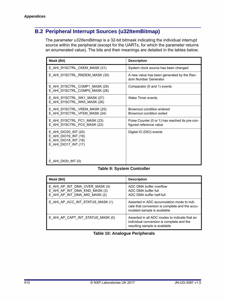
Appendices
B.2 Peripheral Interrupt Sources (u32ItemBitmap)
The parameter u32ItemBitmap is a 32-bit bitmask indicating the individual interrupt source within the peripheral (except for the UARTs, for which the parameter returns an enumerated value). The bits and their meanings are detailed in the tables below.
Mask (Bit) Description
E_AHI_SYSCTRL_CKEM_MASK (31) System clock source has been changed
E_AHI_SYSCTRL_RNDEM_MASK (30) A new value has been generated by the Ran-dom Number Generator
E_AHI_SYSCTRL_COMP1_MASK (29)E_AHI_SYSCTRL_COMP0_MASK (28)
Comparator (0 and 1) events
E_AHI_SYSCTRL_WK1_MASK (27)E_AHI_SYSCTRL_WK0_MASK (26)
Wake Timer events
E_AHI_SYSCTRL_VREM_MASK (25) E_AHI_SYSCTRL_VFEM_MASK (24)
Brownout condition enteredBrownout condition exited
E_AHI_SYSCTRL_PC1_MASK (23) E_AHI_SYSCTRL_PC0_MASK (22)
Pulse Counter (0 or 1) has reached its pre-con-figured reference value
E_AHI_DIO20_INT (20)E_AHI_DIO19_INT (19)E_AHI_DIO18_INT (18)E_AHI_DIO17_INT (17)...E_AHI_DIO0_INT (0)
Digital IO (DIO) events
Table 9: System Controller
Mask (Bit) Description
E_AHI_AP_INT_DMA_OVER_MASK (4)E_AHI_AP_INT_DMA_END_MASK (3)E_AHI_AP_INT_DMA_MID_MASK (2)
ADC DMA buffer overflowADC DMA buffer fullADC DMA buffer half-full
E_AHI_AP_ACC_INT_STATUS_MASK (1) Asserted in ADC accumulation mode to indi-cate that conversion is complete and the accu-mulated sample is available
E_AHI_AP_CAPT_INT_STATUS_MASK (0) Asserted in all ADC modes to indicate that an individual conversion is complete and the resulting sample is available
Table 10: Analogue Peripherals
410 © NXP Laboratories UK 2017 JN-UG-3087 v1.5
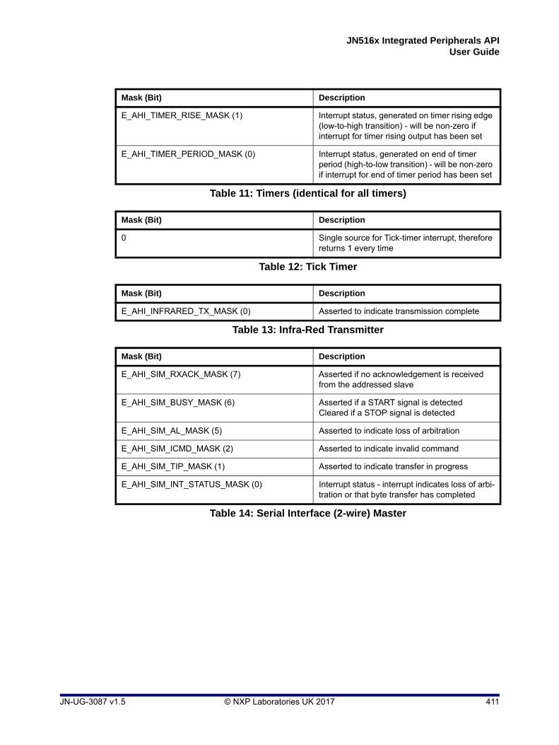
JN516x Integrated Peripherals APIUser Guide
Mask (Bit) Description
E_AHI_TIMER_RISE_MASK (1) Interrupt status, generated on timer rising edge (low-to-high transition) - will be non-zero if interrupt for timer rising output has been set
E_AHI_TIMER_PERIOD_MASK (0) Interrupt status, generated on end of timer period (high-to-low transition) - will be non-zero if interrupt for end of timer period has been set
Table 11: Timers (identical for all timers)
Mask (Bit) Description
0 Single source for Tick-timer interrupt, therefore returns 1 every time
Table 12: Tick Timer
Mask (Bit) Description
E_AHI_INFRARED_TX_MASK (0) Asserted to indicate transmission complete
Table 13: Infra-Red Transmitter
Mask (Bit) Description
E_AHI_SIM_RXACK_MASK (7) Asserted if no acknowledgement is received from the addressed slave
E_AHI_SIM_BUSY_MASK (6) Asserted if a START signal is detectedCleared if a STOP signal is detected
E_AHI_SIM_AL_MASK (5) Asserted to indicate loss of arbitration
E_AHI_SIM_ICMD_MASK (2) Asserted to indicate invalid command
E_AHI_SIM_TIP_MASK (1) Asserted to indicate transfer in progress
E_AHI_SIM_INT_STATUS_MASK (0) Interrupt status - interrupt indicates loss of arbi-tration or that byte transfer has completed
Table 14: Serial Interface (2-wire) Master
JN-UG-3087 v1.5 © NXP Laboratories UK 2017 411

Appendices
Mask (Bit) Description
E_AHI_SIS_ERROR_MASK (4) I2C protocol error
E_AHI_SIS_LAST_DATA_MASK (3) Last data transferred (end of burst)
E_AHI_SIS_DATA_WA_MASK (2) Buffer contains data to be read by SI slave
E_AHI_SIS_DATA_RTKN_MASK (1) Data taken from buffer by SI master (buffer free for next data to be loaded)
E_AHI_SIS_DATA_RR_MASK (0) Buffer needs loading with data for SI master
Table 15: Serial Interface (2-wire) Slave
Mask (Bit) Description
E_AHI_SPIM_TX_MASK (0) Transfer has completed
Table 16: SPI Master
Mask (Bit) Description
E_AHI_SPIS_INT_RX_FIRST_MASK (0) Data has been received in the Receive FIFO, which was previously empty
E_AHI_SPIS_INT_TX_LAST_MASK (1) Last remaining byte in Transmit FIFO has been transmitted, leaving the buffer empty
E_AHI_SPIS_INT_RX_CLIMB_MASK (2) Fill-level of Receive FIFO has risen beyond the configured threshold level
E_AHI_SPIS_INT_TX_FALL_MASK (3) Fill-level of Transmit FIFO has fallen below the configured threshold level
E_AHI_SPIS_INT_RX_OVER_MASK (4) Data was received but Receive FIFO was full or busy (so data was discarded)
E_AHI_SPIS_INT_TX_OVER_MASK (5) Transmit FIFO was written to but was full
E_AHI_SPIS_INT_RX_UNDER_MASK (6) Receive FIFO was read but was empty
E_AHI_SPIS_INT_TX_UNDER_MASK (7) Transmission was attempted but Transmit FIFO was empty or not ready (so 0x00 was transmitted over the SPI bus)
E_AHI_SPIS_INT_RX_TIMEOUT_MASK (8) A Receive timeout has occurred (no further data has been received within this period)
Table 17: SPI Slave
412 © NXP Laboratories UK 2017 JN-UG-3087 v1.5

JN516x Integrated Peripherals APIUser Guide
For the UART interrupts, u32ItemBitmap returns the following enumerated values:
Table 18 lists the UART interrupts from highest priority to lowest priority.
Enumerated Value Description (and Priority)
E_AHI_UART_INT_RXLINE (3) Receive line status (highest priority)
E_AHI_UART_INT_RXDATA (2) Receive data available (next highest priority)
E_AHI_UART_INT_TIMEOUT (6) Time-out indication (next highest priority)
E_AHI_UART_INT_TX (1) Transmit FIFO empty (next highest priority)
E_AHI_UART_INT_MODEM (0) Modem status (lowest priority)
Table 18: UART (identical for both UARTs)
JN-UG-3087 v1.5 © NXP Laboratories UK 2017 413

Appendices
414 © NXP Laboratories UK 2017 JN-UG-3087 v1.5

JN516x Integrated Peripherals APIUser Guide
Revision History
Version Date Comments
1.0 22-Nov-2012 First release
1.1 22-Aug-2013 EEPROM functions added and various other modifications/correc-tions made
1.2 22-Apr-2015 Updated for JN5169 and various modifications/corrections made
1.3 2-June-2015 Added function vAHI_RadioSetReducedInputPower() for JN5169
1.4 3-Feb-2016 Minor modifications/corrections made, including NXP web address updates
1.5 26-Apr-2017 Signals corrected in description of vAHI_ComparatorEnable()
JN-UG-3087 v1.5 © NXP Laboratories UK 2017 415

JN516x Integrated Peripherals APIUser Guide
Important Notice
Limited warranty and liability - Information in this document is believed to be accurate and reliable. However, NXP Semiconductors does not give any representations or warranties, expressed or implied, as to the accuracy or completeness of such information and shall have no liability for the consequences of use of such information. NXP Semiconductors takes no responsibility for the content in this document if provided by an information source outside of NXP Semiconductors.
In no event shall NXP Semiconductors be liable for any indirect, incidental, punitive, special or consequential damages (including - without limitation - lost profits, lost savings, business interruption, costs related to the removal or replacement of any products or rework charges) whether or not such damages are based on tort (including negligence), warranty, breach of contract or any other legal theory.
Notwithstanding any damages that customer might incur for any reason whatsoever, NXP Semiconductors' aggregate and cumulative liability towards customer for the products described herein shall be limited in accordance with the Terms and conditions of commercial sale of NXP Semiconductors.
Right to make changes - NXP Semiconductors reserves the right to make changes to information published in this document, including without limitation specifications and product descriptions, at any time and without notice. This document supersedes and replaces all information supplied prior to the publication hereof.
Suitability for use - NXP Semiconductors products are not designed, authorized or warranted to be suitable for use in life support, life-critical or safety-critical systems or equipment, nor in applications where failure or malfunction of an NXP Semiconductors product can reasonably be expected to result in personal injury, death or severe property or environmental damage. NXP Semiconductors and its suppliers accept no liability for inclusion and/or use of NXP Semiconductors products in such equipment or applications and therefore such inclusion and/or use is at the customer's own risk.
Applications - Applications that are described herein for any of these products are for illustrative purposes only. NXP Semiconductors makes no representation or warranty that such applications will be suitable for the specified use without further testing or modification.
Customers are responsible for the design and operation of their applications and products using NXP Semiconductors products, and NXP Semiconductors accepts no liability for any assistance with applications or customer product design. It is customer's sole responsibility to determine whether the NXP Semiconductors product is suitable and fit for the customer's applications and products planned, as well as for the planned application and use of customer's third party customer(s). Customers should provide appropriate design and operating safeguards to minimize the risks associated with their applications and products.
NXP Semiconductors does not accept any liability related to any default, damage, costs or problem which is based on any weakness or default in the customer's applications or products, or the application or use by customer's third party customer(s). Customer is responsible for doing all necessary testing for the customer's applications and products using NXP Semiconductors products in order to avoid a default of the applications and the products or of the application or use by customer's third party customer(s). NXP does not accept any liability in this respect.
Export control - This document as well as the item(s) described herein may be subject to export control regulations. Export might require a prior authorization from competent authorities.
NXP Semiconductors
For online support resources and contact details of your local NXP office or distributor, refer to:
www.nxp.com
416 © NXP Laboratories UK 2017 JN-UG-3087 v1.5