ISTANBUL TECHNICAL UNIVERSITY F GRADUATE SCHOOL OF …
142
ISTANBUL TECHNICAL UNIVERSITY F GRADUATE SCHOOL OF SCIENCE ENGINEERING AND TECHNOLOGY BANDWIDTH ENHANCEMENT TECHNIQUES FOR CMOS TRANSIMPEDANCE AMPLIFIER Ph.D. THESIS Jawdat ABU TAHA Department of Electronics and Communication Engineering Electronics Engineering Programme FEBRUARY 2016
Transcript of ISTANBUL TECHNICAL UNIVERSITY F GRADUATE SCHOOL OF …

ISTANBUL TECHNICAL UNIVERSITY F GRADUATE SCHOOL OF SCIENCE
ENGINEERING AND TECHNOLOGY
BANDWIDTH ENHANCEMENT TECHNIQUESFOR CMOS TRANSIMPEDANCE AMPLIFIER
Ph.D. THESIS
Jawdat ABU TAHA
Department of Electronics and Communication Engineering
Electronics Engineering Programme
FEBRUARY 2016


ISTANBUL TECHNICAL UNIVERSITY F GRADUATE SCHOOL OF SCIENCE
ENGINEERING AND TECHNOLOGY
BANDWIDTH ENHANCEMENT TECHNIQUESFOR CMOS TRANSIMPEDANCE AMPLIFIER
Ph.D. THESIS
Jawdat ABU TAHA(504112206)
Department of Electronics and Communication Engineering
Electronics Engineering Programme
Thesis Advisor: Associate Prof. Dr. Metin YAZGI
FEBRUARY 2016


ISTANBUL TEKNIK ÜNIVERSITESI F FEN BILIMLERI ENSTITÜSÜ
CMOS TRANSFEREMPEDANS KUVVETLENDIRICININBANTGENISLIGI BASARIMINI GELISTIRMEYE YÖNELIK TEKNIKLER
DOKTORA TEZI
Jawdat ABU TAHA(504112206)
Elektronik ve Haberlesme Mühendisligi Anabilim Dalı
Elektronik Mühendisligi Programı
Tez Danısmanı: Associate Prof. Dr. Metin YAZGI
SUBAT 2016


Jawdat ABU TAHA, a Ph.D. student of ITU Graduate School of Science Engineer-ing and Technology 504112206 successfully defended the thesis entitled “BAND-WIDTH ENHANCEMENT TECHNIQUES FOR CMOS TRANSIMPEDANCE AM-PLIFIER”, which he/she prepared after fulfilling the requirements specified in the as-sociated legislations, before the jury whose signatures are below.
Thesis Advisor : Associate Prof. Dr. Metin YAZGI ..............................Istanbul Technical University
Jury Members : Prof. Dr. Mustafa Karaman ..............................Istanbul Technical University
Prof. Dr. Ismail Serdar Özoguz ..............................Istanbul Technical University
Assistant Prof. Dr. Merih Yıldız ..............................Dogus University
Assistant Prof. Dr. Ramazan Köprü ..............................ISIK University
Date of Submission : 26 January 2016Date of Defense : 17 February 2016
v

vi

To my spouse and children,
vii

viii

FOREWORD
First and foremost, I give a big thanks to God Almighty for giving me this opportunityto do this thesis and as well granting me the capability and strength to finishsuccessfully. This thesis appears in its current form due to the assistance and guidanceof several people whom I would profoundly like to offer my sincere appreciation
My sincere appreciation highly goes to my supervisor Doç. Dr. Metin YAZGI,who, from the start of this research gave his full support for my research and as wellprovided the computational resources and scientific basis that made this work possibleand also to thank him for being always available for open discussions. His personalguidance, constructive and criticizing comments with broaden knowledge have gone along way to helping me reach greater heights throughout my research and during thewriting of this thesis.
I am deeply grateful to Prof. Dr. Mustafa Karaman for giving me the opportunity tojoin their team, and for giving me access to the laboratory and other research facilities.Without their precious supports, it would not have been possible to conduct thisresearch. I also want to thank him for his encouragements, helps, and providing mewith all the necessary facilities for the research.
I would like to thank the rest of my thesis committee: Prof. Mustafa Karaman,Yrd.Doç.Dr. Merih Yıldız, Prof. Dr. Ismail Serdar Özoguz , and Yrd.Doç.Dr.Ramazan Köprü, for their encouragement, insightful comments, and questionableimprovements.
Finally, and most importantly, I would love to express my greatest gratitude to myfamily and friends, especially my wife Najwa, for their permanent support, greatencouragement, infinite patience and meticulous care, which played a very importantrole in the completion of this thesis.Thank you all, I am indebted to you all and will forever remain grateful.
FEBRUARY 2016 Jawdat ABU TAHA
ix

x

TABLE OF CONTENTS
Page
FOREWORD........................................................................................................... ixTABLE OF CONTENTS........................................................................................ xiABBREVIATIONS ................................................................................................. xiiiLIST OF TABLES .................................................................................................. xvLIST OF FIGURES ................................................................................................xviiSUMMARY ............................................................................................................. xxiÖZET ....................................................................................................................... xxv1. INTRODUCTION .............................................................................................. 1
1.1 CMOS transimpedance amplifier (TIA)......................................................... 31.2 Literature summery of CMOS TIAs............................................................... 41.3 Research motivation ....................................................................................... 81.4 Objectives and contributions .......................................................................... 101.5 Organization of the thesis ............................................................................... 11
2. BACKGROUND THEORY OF THE TRANSIMPEDANCE AMPLIFIER 132.1 Important specifications.................................................................................. 132.2 TIA topologies ............................................................................................... 14
2.2.1 Open loop topologies ............................................................................. 142.2.1.1 Single resistor TIA........................................................................... 142.2.1.2 Common gate TIA ........................................................................... 15
2.2.2 Closed loop topologies ........................................................................... 162.2.2.1 Regulated-cascode TIA ................................................................... 162.2.2.2 Shunt-shunt feedback TIA............................................................... 18
3. BANDWIDTH ENHANCEMENT TECHNIQUES FOR CMOS TIAs ........ 213.1 Cherry Hooper amplifier................................................................................. 213.2 Capacitive peaking ......................................................................................... 243.3 Source degeneration ....................................................................................... 253.4 Inductive peaking ........................................................................................... 26
3.4.1 Shunt peaking ......................................................................................... 263.4.2 Series peaking......................................................................................... 283.4.3 Shunt–series peaking circuit................................................................... 303.4.4 T-coil peaking technique ........................................................................ 303.4.5 π-type inductor peaking (PIP) ................................................................ 34
3.5 Current-mode signaling .................................................................................. 353.6 Distributed amplification ................................................................................ 363.7 Chapter summary............................................................................................ 37
xi

4. IMPROVE THE BANDWIDTH OF TRANSIMPEDANCE AMPLIFIERUSING NEGATIVE IMPEDANCE CIRCUIT .................................................... 39
4.1 Introduction .................................................................................................... 394.2 Principle of negative impedance circuit ......................................................... 404.3 The negative impedance (NI) circuit .............................................................. 434.4 Configuration of the proposed TIA with negative impedance NI circuit ....... 454.5 Active inductor (AI) ....................................................................................... 464.6 Noise analysis of the proposed transimpedance amplifier ............................. 484.7 Simulation results .......................................................................................... 504.8 Conclusion...................................................................................................... 54
5. IMPROVE THE BANDWIDTH OF TRANSIMPEDANCE AMPLIFIERUSING MATCHING TECHNIQUE..................................................................... 57
5.1 Introduction .................................................................................................... 575.2 The proposed TIA design .............................................................................. 585.3 Input matching analysis ................................................................................. 595.4 Output matching analysis .............................................................................. 605.5 Input noise analysis ........................................................................................ 625.6 Design example and simulation results .......................................................... 645.7 Conclusion...................................................................................................... 68
6. IMPROVE THE BANDWIDTH OF TRANSIMPEDANCE AMPLIFIERBY MODIFICATION THE INPUT CIRCUIT.................................................... 69
6.1 Introduction .................................................................................................... 696.2 Regulated common gate (RCG) input stage ................................................... 70
6.2.1 Conventional RCG input stage ............................................................... 706.2.2 Modified RCG input stage...................................................................... 71
6.3 The capacitance degeneration......................................................................... 726.4 The proposed TIA........................................................................................... 746.5 Noise analysis ................................................................................................. 756.6 Simulation results ........................................................................................... 776.7 Conclusion...................................................................................................... 79
7. IMPROVING THE BANDWIDTH PERFORMANCE BY USING ACASCODE CURRENT MIRROR WITH RESISTIVE COMPENSATIONTECHNIQUE AND A LADDER MATCHING NETWORK............................. 81
7.1 Introduction .................................................................................................... 817.2 Regulated common gate (RCG) TIA with ladder matching network............. 827.3 Cascode current mirror with resistive compensation technique .................... 857.4 The proposed TIA ......................................................................................... 867.5 Noise analysis ................................................................................................. 877.6 Simulation results ........................................................................................... 887.7 Conclusion...................................................................................................... 91
8. CONCLUSIONS AND RECOMMENDATIONS ........................................... 938.1 Future works ................................................................................................... 97
REFERENCES........................................................................................................ 99CURRICULUM VITAE......................................................................................... 112
xii

ABBREVIATIONS
EMI : Electromagnetic InterferenceOC : Optical CommunicationLED : Light Emitting DiodeTIA : Transimpedance AmplifierMUX : MultiplexerDMUX : DemultiplexerLA : Limiting AmplifierTX : TransmitterRX : ReceiverGbps : GegabitsPLL : Phase Locked LoopCDR : Clock and Data RecoveryAGC : Automatic Gain ControlISI : Inter Symbol InterferenceFoM : Figure of MeritBW : BandwidthCMOS : Complementary Metal Oxide SemiconductorCpd : Photodiode CapacitanceQ : Gain PeakingC : CapacitorL : InductorR : ResistorGm : TransconductanceRGC : Regulated CascodeCHRT : Chartered Semiconductor ManufacturingRTRN : Reverse Triple Resonance NetworkVLSI : Very Large Scale IntegrationIC : Integrated CircuitSOC : System On ChipZT IA : Transimpedance Gainτg( f ) : Group Delayi2n : Input Referred Noise CurrentCG : Common GateCS : Common SourceA : DC Voltage GainCHT : Cherry Hooper Topologyω : Cut-Off Frequencyη : Bandwidth Improvement Factor
xiii

LM : Mutual Inductanceτ : Time ConstantDA : Distributed AmplifierNI : Negative Impedancep : PoleCgs : Gate-Source CapacitanceAI : Active Inductorg : ConductanceT : Temperature (Kelvin)γ : Bias Dependent FactorkB : Boltzmann’s Constantgd0 : Zero Bias of Transconductance
δ : Gate Noise FactorRF : Radio Frequency
xiv

LIST OF TABLES
Page
Table 4.1 : Performance Comparison of Recent CMOS TIAs.............................. 54Table 5.1 : Performance Comparison of Recent CMOS TIAs.............................. 68Table 6.1 : Performance summary and comparison with the other works using
0.18µm CMOS technology. ................................................................ 80Table 7.1 : Performance Comparison of Recent CMOS TIAs. ............................ 91Table 8.1 : Summary of TIA bandwidth enhancement techniques. ...................... 94
xv

xvi

LIST OF FIGURES
Page
Figure 1.1 : (a) Simple optical system, (b) addition of driver and amplifier [1]. .. 2Figure 1.2 : Basic Optical Communication System [1]. ....................................... 3Figure 2.1 : Input Referred Noise Current. ........................................................... 14Figure 2.2 : (a) Circuit diagram of a single resistor TIA b) A single resistor
with Photodiode Model....................................................................... 15Figure 2.3 : Common-gate TIA............................................................................. 16Figure 2.4 : Regulated Common Gate TIA. .......................................................... 17Figure 2.5 : A shunt-shunt feedback TIA.............................................................. 18Figure 3.1 : The fundamental structure Cherry-Hooper topology [2]................... 22Figure 3.2 : A modified Cherry-Hooper TIA with a common gate input stage [2]. 22Figure 3.3 : Capacitive peaking [3]. ...................................................................... 24Figure 3.4 : Source degeneration [3, 4]. ................................................................ 25Figure 3.5 : Shunt Peaking [3, 5, 6]. ...................................................................... 27Figure 3.6 : Shunt peaking circuit with three poles and two zeros. ...................... 27Figure 3.7 : Series Peaking Circuit. ...................................................................... 28Figure 3.8 : Series peaking circuit with three poles. ............................................. 29Figure 3.9 : The shunt–series peaking circuit. ...................................................... 30Figure 3.10: a) The basic T-coil circuit. b) an equivalent circuit, with no
magnetic coupling between the coils c) a simplified impedancecircuit. ................................................................................................. 31
Figure 3.11: a) The basic T-coil circuit. b) an equivalent circuit, with nomagnetic coupling between the coils c) a simplified impedancecircuit. ................................................................................................. 31
Figure 3.12: T-coil network with three poles. ........................................................ 33Figure 3.13: T-coil network with three poles. ........................................................ 34Figure 3.14: The frequency response of the published inductive peaking
techniques [5, 7]. ................................................................................ 34Figure 3.15: Small-signal equivalent circuit of the PIP model [8]......................... 34Figure 3.16: The normalized frequency response of the inductor peaking (PIP)
[9]........................................................................................................ 35Figure 3.17: Distributed amplifiers [10]................................................................. 36Figure 4.1 : Block diagram for the traditional resistive feedback TIA with NI
circuit. ................................................................................................. 41Figure 4.2 : Small signal equivalent circuit of TIA............................................... 43Figure 4.3 : (a) Negative impedance (NI) circuit. (b) Small signal equivalent
model of the NI. .................................................................................. 44Figure 4.4 : The real component of the input impedance of ZNI . ......................... 45Figure 4.5 : The imaginary component of the input impedance of ZNI . ............... 45
xvii

Figure 4.6 : Variation of NI capacitance over the frequency................................. 46Figure 4.7 : A proposed circuit digram of the T IA. .............................................. 46Figure 4.8 : Circuit schematic of floating active inductor. .................................... 47Figure 4.9 : (a) equivalent small-signal of half-circuit of Floating active
inductor (b) Simplified model of active inductor. ............................... 48Figure 4.10: (a) Noise model of MOS transistor, (b) Noise model of a resistor. .. 48Figure 4.11: TIA realization................................................................................... 50Figure 4.12: Simulation results comparison of the frequency response of TIA
with and without NI. ........................................................................... 51Figure 4.13: Frequency response of the proposed TIA for four different values
of Cpd . ................................................................................................. 51Figure 4.14: Spectral density of the input noise current as function of frequency. 52Figure 4.15: Measured group delay variation of TIA for different values of Cpd .. 52Figure 4.16: The frequency response of the TIA (schematic and extracted). ........ 53Figure 4.17: Monte Carlo simulation results for the frequency response for 100
samples................................................................................................ 53Figure 4.18: Transient response of the TIA under different corners...................... 54Figure 4.19: Layout of the TIA. ............................................................................. 54Figure 5.1 : Schematic of proposed TIA with matching networks. ...................... 59Figure 5.2 : Small signal model of the input matching of Figure 5.1. .................. 59Figure 5.3 : Simplified small signal model to calculate of Zin. ............................. 59Figure 5.4 : (a) The small signal model to calculate Zout (b) The small
signal model to calculate Yind1′ at drain of M′1. ................................... 61Figure 5.5 : Small signal noise model of the TIA. ................................................ 62Figure 5.6 : The frequency response for Cpd = 50 f F . ......................................... 65Figure 5.7 : The frequency response for different values of Cpd . ......................... 65Figure 5.8 : The input noise current spectral density against the photodiode
capacitance Cpd . .................................................................................. 66Figure 5.9 : The group delay variation of the TIA. .............................................. 66Figure 5.10: Monte Carlo simulation results for the frequency response for 100
samples................................................................................................ 67Figure 5.11: Transient response of the TIA under different corners. .................... 67Figure 5.12: Layout of the TIA. ............................................................................ 67Figure 6.1 : Regulated common gate (RCG) TIA................................................. 71Figure 6.2 : The input part of a narrow band RCG TIA........................................ 71Figure 6.3 : The input part of RCG TIA with two input branches........................ 73Figure 6.4 : Configuration of capacitive degeneration. ......................................... 73Figure 6.5 : The proposed configuration of capacitive degeneration. ................... 74Figure 6.6 : Schematic of proposed RCG TIA...................................................... 75Figure 6.7 : Modified RCG TIA with noise sources. ............................................ 76Figure 6.8 : The layout of the proposed TIA. ....................................................... 77Figure 6.9 : Frequency response results of the TIA. ............................................. 78Figure 6.10: Spectral density of the input noise current. ....................................... 78Figure 6.11: The group delay variation of TIA...................................................... 79Figure 6.12: Transient response of the TIA at different process corners. .............. 79Figure 7.1 : Regulated common gate (RCG) TIA................................................. 82
xviii

Figure 7.2 : RCG TIA configuration with ladder network.................................... 84Figure 7.3 : Simplified model of RCG with ladder network................................. 84Figure 7.4 : Cascode current mirror with resistive compensation......................... 85Figure 7.5 : Simplified model of compensated cascode current mirror. ............... 85Figure 7.6 : Schematic of proposed RCG TIA...................................................... 86Figure 7.7 : Layout of TIA.................................................................................... 88Figure 7.8 : The frequency response results of the TIA........................................ 89Figure 7.9 : Spectral density of the input noise current as a function of frequency. 89Figure 7.10: The group delay variation of TIA...................................................... 89Figure 7.11: Monte Carlo simulation results for frequency response for 100
samples................................................................................................ 90Figure 7.12: Transient response of the TIA under different corners...................... 90Figure 8.1 : Performances comparison of TIA bandwidth enhancement
techniques. .......................................................................................... 95
xix

xx

BANDWIDTH ENHANCEMENT TECHNIQUESFOR CMOS TRANSIMPEDANCE AMPLIFIER
SUMMARY
The accelerated development of integrated systems in the communication technologyand their application are among the significant technologies that have developedthe information era by empowering high-speed computation and communicationtechnique besides high-speed access to stored data. The continuous growth demandfor high-speed transport of information has rekindled optical communications, leadingto derived research on high-speed device and integrated circuit design. Among theavailable medium to transfer the data, optical fibers have the best performance. Opticalfibers are very common these days to transport very high rate digital data. Suchhigh speed data rates can be transported over kilometers of optical fiber and withoutsignificant loss. Normally loss is very low when the signal is transmitted using lightrather than electrical signal. These fibers also have the advantage of being low costin addition to improvement of performance. In state-of-the-art technology, fiber opticdevices and systems are evidently employed to realize very high data rates. Fiber opticcommunication is a solution because high data rates can be transmitted through thishigh capacity cable with high performance.
Traditionally, analog circuits used in optical communication systems are implementedusing Gallium Arsenide (GaAs) or Indium Phosphide (InP) technologies. Theseprocesses are designed for high speed circuits, and have been traditionally theonly technologies able to produce the high bandwidth circuits required in opticalcommunication systems. However, due to the aggressive scaling of the CMOS process,it is now becoming possible to design high performance analog circuits in CMOS. Theprimary advantage of moving to a CMOS process is a dramatic reduction in cost due toits widespread use in high volume digital circuits. Another advantage of using CMOSis its ability to integrate digital and analog circuits onto the same substrate.
Transimpedance amplifier (TIAs) is the first building block in the opticalcommunication receiver that converts the small signal current to a correspondingoutput voltage signal. The important requirements of a typical TIA are largebandwidth, high transimpedance gain, low noise, low power consumption, and smallgroup delay variation.
Current developments in nanoscale technologies made it economically feasible todesign CMOS transimpedance amplifier (TIA) that satisfies the stringent performancesnecessary for the front-end optical transceivers applications such as low power, lowcost and high integration which offers the most economical solution in the consumerapplication market.
In designing of TIA, the two major factors that must be considered are the bandwidthand the input sensitivity. The bandwidth of TIA is usually limited by the parasitic
xxi

capacitance at the input stage, and it can be calculated by its RC time constantcontributed by photodiode capacitance, parasitic capacitance and input resistance ofthe amplifier. The sensitivity is affected by the input current noise of the TIA.Therefore it is challenge to choose the suitable circuit topology that provides anoptimal trade-off between bandwidth and input signal sensitivity for TIA.
This thesis is an attempt toward providing novel techniques to extend the bandwidth ofthe transimpedance amplifier using CMOS technology. Different approaches used toimprove the bandwidth of CMOS TIAs are covered. Moreover, this research providesthe necessary background knowledge to fully understand the analysis and design of thetransimpedance amplifier (TIA).
Bridging the gap between system and circuit design is done by: Understanding thebandwidth expansion by mathematical analysis. Introducing new circuit architecturesthat can be realized. Demonstrating implementation of the proposed designs usingextensive simulations in CMOS technology.
It is shown in this thesis that, using a negative impedance NI circuit can be used forbandwidth extension. In our application, the negative impedance is incorporated intothe output pole of TIA. The bandwidth can be improved by increasing the gain (A =gmRout) and by maintaining the same time constant at the output pole. A better gain Acan be obtained if the output resistance Rout is increased. Increasing Rout can be doneby placing a negative resistance RIN in parallel with the output resistance Rout . In orderto maintain the same time constant at the output node, a negative capacitance can beused. It have been reported that, the shunt feedback architecture is used to improvethe bandwidth of TIA. Increasing the gain A effectively decreases the input resistanceand hence increase the frequency of the input pole due to feedback. As a result, animprovement of the bandwidth can be obtained. Using the proposed topology, a wideband transimpedance amplifier with a bandwidth of 7 GHz and transimpedance gainof 54.3 dBΩ is achieved. The total power consumption of the proposed TIA from the1.8 V power supply is 29 mW . The TIA is designed in 0.18 µm CMOS technology.The simulated input referred noise current spectral density is 5.9 pA/
√Hz and the TIA
occupies 230µm×45µm of area.
Furthermore, a wide band TIA is designed using the matching technique. It is shownthat by simultaneously using of series input matching topology and T-output matchingnetwork, the bandwidth of the TIA can be obviously improved. This methodologyis supported by a design example in a 0.18 µm CMOS technology. The post layoutsimulation results show a bandwidth of 20 GHz with 50 f F photodiode capacitance, atransimpedance gain of 52.6 dBΩ, 11 pA/
√Hz input referred noise and group delay
less than 8.3 ps. The TIA dissipates 1.3 mW from a 1.8 V supply voltage.
In addition, a new design possessing to extend the bandwidth of the TIA is presented.This TIA employs a parallel combination of two series resonate circuits withdifferent resonate frequencies on the conventional regulated common gate (RGC)architecture. In the proposed TIA, a capacitance degeneration and series inductivepeaking technique are used for pole-zero elimination. The TIA is implemented in a0.18 µm CMOS process, where a 100 f F photodiode is considered. The post layoutsimulation results show a transimpedance gain of 53 dBΩ transimpedance gain alongwith a 13 GHz bandwidth. The designed TIA consumes 11 mW from a 1.8 V supply,and its group-delay variation is 5 ps with 24 pA/
√Hz input referred noise.
xxii

In the last phase of the work, a technique to enhance the bandwidth of the regulatedcommon gate (RCG) transimpedance amplifier is described. The technique is basedon using a cascode current mirror with resistive compensation technique and a laddermatching network. In order to verify the operation and the performance of the proposedtechnique, a CMOS design example is designed using the 0.18µm CMOS processtechnology. The post layout simulation results show that, the proposed TIA achieveda bandwidth of 8.4 GHz, a transimpedance gain of 51.3 dBΩ and input referred noisecurrent spectral density of 20 pA/
√Hz. The average group-delay variation is 4 ps over
the bandwidth and the TIA consumes 17.8 mW from a 1.8 V supply.
To sum up, this thesis focuses on various design techniques of transimpedanceamplifier (TIA) that improves the bandwidth performance. We believe that, ourapproaches and techniques exhibit a path which other future researchers can followand as well refer to as their researching domain and also could be used in their researchapplications.
xxiii

xxiv
CMOS TRANSFEREMPEDANS KUVVETLENDIRICININBANTGENISLIGI BASARIMINI GELISTIRMEYE YÖNELIK TEKNIKLER
ÖZET
Bandwidth Enhancment techniques for CMOS Transimpedance amplifier
CMOS Transferempedans Kuvvetlendiricinin bandgenisligi basarımını gelistirmeyeyönelik teknikler haberlesme teknolojisinde ve uygulamalarında ortaya çıkan hızlıgelismeler ve uygulamalar verilere hızlı erisim avantajı yanında hızlı hesaplama vehaberlesme tekniklerine imkan veren bir bilgi çagını ortaya çıkarmıstır. Sürekli artanhızlı bilgi transferi ihtiyacı, hızlı elemanların ve tümdevrelerin tasarımına yönelikarastırmalara liderlik eden optik haberlesme teknigini dogurmustur.
Veri iletimi için mevcut ortamlar arasında optik fiber yapıları en iyi basarımısunmaktadır. Günümüzde optik fiberler çok yogun sayısal veri transferinde geniskullanım alanı bulmaktadır. Yogun veri aktarımı kilometrelerce uzunlukta optikfiberler üzerinde önemli bir kayıp olmaksızın yapılabilmektedir. Normal sartlarda,isaret aktarımının ısık ile yapılması durumunda ortaya çıkan kayıp elektriksel yollayapılan aktarıma gore daha düsüktür. Optik fiberler genel basarımı iyilestirmeninyanında düsük maliyet avantajını da sunmaktadır. En yüksek teknolojilerde, optik fiberelemanları ve sistemleri çok yogun veri aktarımı amacıyla kullanılmaktadır. Sonuçolarak optik fiber teknolojisi düsük kayıpla çok yogun veri aktarımını az maliyetlesunabilen bir teknoloji olarak günümüzde çok önemli bir konuma sahiptir.
Genel olarak, optik haberlesme sistemlerinde kullanılan analog devreler GalyumArsenik (GaAs) veya Indiyum Fosfid (InP) teknolojileri ile üretilmektedir. Buprosesler yüksek hızlı devreler için olusturulmakta olup optik haberlesme sistemlerininihtiyaç duydugu yüksek band genisligine sahip devreleri üretmek için genellikle tekalternatif olarak karsımıza çıkmaktadırlar. Bununla birlikte, CMOS proseslerindeortaya çıkan hızlı gelismeler sayesinde daha yüksek basarımlara sahip analog devreleriCMOS proses kullanarak tasarlama ve gerçeklestirme imkanları gittikçe artmaktadır.CMOS prosesin tercih edilmesine sebep olan en önemli avantaj maliyetlerde ortayaçıkan büyük düsüstür. CMOS proseslerin maliyetinin düsük olmasının sebebi, büyükalan kullanımı gerektiren sayısal devre gerçeklestirmelerinde çok genis bir kullanımasahip olmasıdır. CMOS prosesin diger bir avantajı sayısal ve analog devrelerin aynıtaban üzerinde gerçeklestirilmesine imkan vermesidir.
Transferempedans kuvvetlendirici (TIA) optik haberlesme alıcılarındaki ilk blok olupgirisindeki akımı çıkısında gerilime dönüstürmektedir. Tipik bir TIA’nın önemlibasarım ihtiyaçları genis bandgenisligi, yüksek transferempedans kazancı, düsükgürültü, düsük güç tüketimi ve küçük grup geçikme degisim aralıgıdır.
Nano teknolojilerdeki güncel gelismeler, optik alıcıların giris katı uygulamalarındagerekli kolay bir sekilde elde edilemeyen basarımları saglayabilen CMOS Transfer-empedans Kuvvetlendiricinin (TIA) tasarımını ekonomik hale getirmistir.
xxv
TIA tasarımında dikkat edilmesi gereken iki önemli mesele bandgenisligi ve girishassasiyetidir. TIA’nın bandgenisligi genellikle giristeki parasitic kapasite tarafındansınırlanmaktadır. TIA’nın bandgenisligi fotodiyot kapasitesi, transistor giris kapasitesive transistor giris direncinin belirledigi RC zaman sabiti ile bulunabilir. Girishassasiyeti ise TIA’nın giris gürültü akımından etkilenmektedir. Bundan dolayıTIA’nın bandgenisligi ve giris isareti hassasiyeti basarımlarını optimum bir sekildetemin eden uygun devre topolojisinin belirlenmesi önemli bir meseledir.
Bu tez, CMOS teknolojisi kullanan Transferempedans Kuvvetlendiricinin band-genisligi basarımını gelistirmeye yönelik yeni teknikler sunan bir çalısmadır. CMOSTIA’nın bandgenisligi basarımını iyilestirmeye yönelik farklı yaklasımlar tez içerisindegösterilmektedir.
Bundan baska, bu çalısma transferempedansı kuvvetlendiricinin analizini ve tasarımınıtam olarak anlamak için gerekli altyapı bilgisini de sunmaktadır. Bu tezde, sistemledevre tasarımı arasındaki boslugu doldurmak için sunlar yapılmıstır: - Band genisligibasarımının arttırılmasının matematiksel analizlerle anlasılması. - Gerçeklestirilebiliryeni devre yapılarının tanıtılması. - Teklif edilen tasarımların CMOS teknolojisiylegerçeklestirilebilirliginin kapsamlı ve detaylı simülasyonlar kullanılarak gösterilmesi.
Sunulan yeni devre yapılarının ilki olarak, negatif empedans devresinin bandgenisligiartısı için kullanılabilecegi bu tezde gösterilmis olup bu teknik bu tezde TIA’nınçıkıs kutpu için uygulanmaktadır. Bandgenisligi, kazancı (gmRout) arttırarak veçıkısta aynı zaman sabiti korunarak arttırılabilir. Çıkıs direnci arttırılarak kazanç(A) yükseltilebilir. Çıkıs direnci çıkısa uygulanacak bir negative direnç devresiile arttırılabilir. Çıkısta aynı zaman sabitini korumak için ise negatif kapasitedevresi kullanılabilir. Daha yüksek kazanç degeri (A) rezistif geribesleme sayesindegiris direncini azaltarak giris kutbunun yükselmesini saglamaktadır. Sonuç olarak,bandgenisligi basarımında bir iyilestirme elde edilebilmektedir. Teklif edilen topolojiile 7GHz bandgenisligine ve 54.3dB’lik kazanca sahip bir TIA tasarlanmıstır. Teklifedilen TIA’nın 1.8V’luk besleme kaynagından çektigi toplam güç 29mW’tır. Teklifedilen TIA’nın 0.18um CMOS proses ile post-serimi yapılmıstır. Benzetimle eldeedilmis giris gürültü akım yogunlugu 5.9pA/ Hz olup kapladıgı alan 230umX45umolmustur.
Tezde bir sonraki çalısmada eslestirme teknigi kullanılarak genis bantlı bsr TIAtasarlanmıstır. Giriste seri empedans eslestirme teknigi ve çıkısta T tipi eslestirmeyapısı birlikte kullanılarak TIA’nın bandgenisligi basarımının iyi bir düzeydeiyilestirilebilecegi gösterilmistir. Bu yaklasım 0.18um CMOS teknolojisi ile yapılmısbir tasarım örnegi ile desteklenmistir. Post serim sonuçları 50fF’lık bir fotodiyotkapasitesi için 20GHz’lik bandgenisligi, 52.6dB’lik transferdirenci kazancı, 8.7pA/Hz ‘lik giris gürültü akımı ve 3pS’den daha az grup geçikmesi basarımılarını vermistir.Bu TIA uygulaması 1.8V’luk besleme kaynagından 1.3mW güç çekmistir.
Tezin üçüncü asamasında TIA band genisligi basarımını arttırmaya yönelik baska biryapı sunulmaktadır. Bu yapı, literatürde bilinen regule edilmis ortak geçitli mimari ilebirlikte farklı rezonans frekanslarına sahip iki rezonans devresinin paralel kullanımınıiçermektedir. Teklif edilen TIA devresinde, kapasite dejenarasyon ve seri endüktiftepe teknikleri kutup-sıfır kompanzasyonu için kullanılmıstır. 100fF’lık fotodiyotkapasitesine sahip bir TIA 0.18um CMOS prosesi ili tasarlanmıstır. Post-serimsonuçları 13GHz’lik bandgenisligi, 53dB’lik transferdirenci kazancı, 24pA/ Hz ‘lik
xxvi

giris gürültü akımı ve 5pS’den daha az grup geçikmesi basarımılarını vermistir. BuTIA uygulaması 1.8V’luk besleme kaynagından 11mW güç çekmistir.
Tezin dördüncü asamasında, regule edilmis ortak geçitli mimari kullanan TIA’nınbandgenisligi basarımını arttırmaya yönelik bir teknik tanıtılmıstır. Bu teknik, resistifkompanzasyon teknigini ve merdiven eslestirme yapısını bir kaskod akım kaynagıile birlikte kullanmaya dayanmaktadır. Bu yapının basarımını göstermek amacıyla,0.18um CMOS prosesi ile bir tasarım yapılmıstır. Post-serim sonuçları 8.4GHz’likbandgenisligi, 51.3dB’lik transferdirenci kazancı, 20pA/ Hz ‘lik giris gürültü akımı ve4pS’den daha az grup geçikmesi basarımılarını vermistir. Bu TIA uygulaması 1.8V’lukbesleme kaynagından 17.8mW güç çekmistir.
Tezin son asamasında, tezde sunulan teknikler ve yapıların kendi aralarındakarsılastırılması verilmektedir. Karsılastırma öncelikli olarak band genisligi,transferempedansı kazancı, gürültü, güç tüketimi, grup geçikme degisim aralıgı vekapladıgı alan için yapılmaktadır. Bunlara ek olarak, sunulan yapıların kullandıgıtekniklerin avantajlı yanları ile birlikte (kararlılık üzerinde olusabilecek negatif etkilergibi) dezavantajlı tarafları da tezin son asamasında verilmektedir.
Tezin son asamasında yapılan karsılastırmalar, en iyi bant genisligi basarımınıneslestirme teknigini kullanan yapıdan elde edildigini göstermektedir. Bununla birliktediger yapıların da band genisligi basarımı üzerinde önemli iyilestirmeler yaptıgı ortayakonulmaktadır. Gürültü açısından ise en yüksek basarımın negatif empedans tekniginikullanan yapıda elde edildigi görülmektedir. Bu yapı aynı zamanda düsük alankullanımı imkanı da sunmaktadır. Tezde sunulan diger iki yapı ise özellikle yüksekdegerli fotodiyot kapasiteleri için incelenmis olup band genisligi basarımı üzerindeönemli iyilestirmeler yaptıkları gösterilmektedir.
Sonuç olarak, bu tezde transferempedans kuvvetlendiricinin bandgenisligi basarımınıiyilestiren farklı teknikler sunulmakta olup bu teknikler ayrıntılı ve karsılastırmalıolarak incelenmektedir. Tezde verilen sonuçlar sunulan yeni tekniklerin basarımlarınınyüksek oldugunu ve literature yeni ve güçlü alternatfiler sunuldugunu göstermektedir.Tezde sunulan yaklasımların ve tekniklerin gelecekte yapılacak benzer arastırmalarahem yardımcı olacak hem de referans olacak nitelikte oldugu düsünülmektedir.
xxvii

xxviii
1. INTRODUCTION
Integrated systems are among the significant technologies that have developed the
information era by empowering high-speed computation and communication technique
besides high-speed access to stored data. The continuous growth demand for
high-speed transport of information has rekindled optical communications, leading to
derived research on high-speed device and integrated circuit design [11].
Nowadays, improvement of faster communication channels is driven by propagation
of the Internet, high-speed microprocessors, and low-cost memory. Moreover, optical
fiber communication also has enormous attraction because of its advantages over
electrical communication, such as data transmission capacity, smaller and lighter
which reduces the cost of laying of the cable, low power consumption, more safety
, better security, less cross-talk, and lower electromagnetic interference (EMI) [12].
Optical communication systems have been used to transfer data in past decades and are
still dominant today due to the creation and development of wideband semiconductor
lasers, low-loss fibers, fast photodetectors, and other high quality optoelectronic
elements [13].
The main objective of an optical communication (OC) network is to transmit a huge
data over a long distance from a transmitter to a receiver by sending pulses of light
through an optical fiber. The simple OC system composes of three main blocks: a
transmitter, an optical fiber, and a receiver as shown in Figure1.1.
• The transmitter generates the optical signal by converting the electrical signal to
optical information as light pulses. The light-emitting diodes (LEDs) and laser
diodes are most commonly devices used as transmitter.
• The receiver converts the light pulses back to electrical current pulses. The
photodetector is the main device of the optical receiver.
• Optical fiber transports the optical data over the significant distance.
1

Figure 1.1 : (a) Simple optical system, (b) addition of driver and amplifier [1].
Due to long or low quality optical fiber, the optical signal attenuates significantly,
as it transfers from one end to the other end and large a part of the optical power
disappears. Therefore, to obtain better performance of an OC, auxiliary building blocks
are used such as laser driver, transimpedance amplifier (TIA), multiplexer (MUX),
demultiplexer (DMUX) , phase locked loop [1].
A laser driver is used to provide large current to the laser and to amplify the laser
output. A transimpedance amplifier (TIA ) amplifies the electrical current with
sufficient bandwidth, converting it to a voltage for further signal processing in the
subsequent stages, with small noise as possible.
Generally, the TIA output signal is smaller than the logic level (approximately
500 mV p− p). So extra amplification is placed in the form of a limiting amplifier (LA).
After boosting the received signal to detectable logic levels, the noise is removed by a
decision circuit. The decision circuit is triggered by a clock and data recovery circuit
which creates a clock signal from the received data.
The complete optical communication system is shown in Figure1.2. The MUX is
used in the transmitter (TX) to convert low speed “parallel” channels to a high speed
serial data stream. Meanwhile, The DMUX is used in the receiver (RX) to regenerate
received serial data stream from original parallel channels. The phase locked loop
(PLL) creates a number of clock pulses to control the MUX.
At the receiver end limiting amplifier (LA) follows the TIA is used to amplify the
output voltage of the TIA to the logical level. In additional, over, a clean-up flip-flop is
placed between the LA and the DMUX to minimize the corruption of received signal
2

Figure 1.2 : Basic Optical Communication System [1].
and circuit noise. The clock and data recovery” (CDR) is used to generate the clock
from the received signal. An automatic gain control (AGC) is employed to obtain
better performance of the TIA.
1.1 CMOS transimpedance amplifier (TIA)
Wideband amplifiers are one of the most important building blocks of any optical
communication system mainly, all amplifiers in the signal path, as the transimpedance
amplifier (TIA) which typically affects cost and determines the overall optical link
performance as speed, signal-to-noise ratio, and sensitivity [14, 15].
The main purpose of TIA is to amplify the small current received from the photodiode
and convert it to a voltage signal. There are important parameters in the design of
transimpedance amplifiers such as bandwidth, gain, noise, power, and supply voltage.
The TIA should have high bandwidth to avoid inter symbol interference (ISI). The
input current to the TIA is very small and therefore the gain should be high enough
to be able to produce an acceptable voltage level for the limiting amplifier. This
voltage is in the level of few mili-volts. Since the input current of TIA is very low,
in order to achieve high signal to noise ratio, the input referred noise of TIA must
be low. So that, the TIA is a wideband, high gain, and low noise amplifier with low
power consumption and low supply voltage [16, 17]. In conclusion, design of TIA
requires the trade-off a number of contradictory performance metrics including gain,
bandwidth, noise, and power consumption which is a big challenge for analog circuit
designers. In current to voltage amplifiers (TIAs), the figure of merit (FoM) is the
3

tansimpedance bandwidth product (ZBW ). This means that the ZBW is traded off
against the bandwidth (BW ). Bandwidth is defined as the upper frequency for which
the transimpedance gain rolls off 3dB below its midband value. Bandwidth is usually
determined by the total capacitance contributed by the photodiode, the transimpedance
amplifier and other parasitic elements present at the optical front-end [18].
Equally important as a large output impedance for amplifier circuits is a small input
impedance. This is because a low input impedance reduces the loading-induced current
error [19]. Also, in applications such as data links over wire channels, a low input
impedance of the receivers is critical to increase the pole frequency at the input as the
channels often have a large capacitance. Reduction of the input-capacitance helps to
improve the bandwidth.
1.2 Literature summery of CMOS TIAs
Current developments in nanoscale technologies made it economically feasible to
design CMOS transimpedance amplifier (TIA) that satisfies the stringent performances
necessary for the front-end optical transceivers applications [20].
The bandwidth requirements of such transimpedance amplifiers continuously improve
following the drive for higher speed systems. While device scaling maintains to deliver
faster transistors with higher cut-off frequencies, it is still necessary to expand the
bandwidth of amplifiers using circuit techniques that allow us to do so for a given
process technology. For the CMOS TIA, the circuit bandwidth is basically limited
by the intrinsic capacitances of the transistors. Over the last few decades; several
bandwidth extension techniques have been developed to improve the bandwidth of
TIAs. The main design concept in these techniques is all related to how to reduce the
impact of the parasitic capacitances on the circuit.
Three approaches, namely current-mode signaling, inductive peaking, and distributed
amplification, are widely used to improve the bandwidth of circuits [21]. Current
mode circuits offer an improved bandwidth because it has low nodal impedances which
decreases time constants of the circuits. In addition the low voltage swing reduces the
time required to charge and discharge the nodes of the circuits [21, 22].
4

The bandwidth or speed of a circuit is set by the time constant of the critical node of the
circuit. An effective way to minimize the effect of the large shunt capacitance of the
critical node is to break the large shunt capacitor into several smaller shunt capacitors
and separate them with inductors such that the large shunt capacitor is replaced with a
distributed LC network or a transmission line [21, 22].
Analui [23] has proposed a technique to isolate between different stages of an amplifier
by using a passive matching networks at the input and output, as well as between the
gain stages of the amplifier to enhance the bandwidth. The proposed passive network is
an inductor and it forms a ladder filter with the parasitic capacitances of devices. The
TIA achieves a 3-dB bandwidth of 9.2 GHz, transimpedance gain of 54dB Ω. This
circuit has been implemented in 0.18 µm BICMOS process using CMOS transistors.
The amount of PD capacitance has been considered 500 f F .
Chien and Chan [24, 25] proposed a bandwidth enhancement of TIA by a
capacitive-peaking design. This technique uses a gain peaking effect of the frequency
response by carefully controlling the capacitance CL loaded at the output node of a
preamplifier, thereby increasing the bandwidth. For many practical applications for
broadening the bandwidth value of Q ranges from 1/2 to 5/6, which corresponds
to the 0− 10% overshoot. Measurement shows that the maximally flat gain curve
(Butterworth response) is obtained at Q = 0.707. The amount of the required gain
peaking (Q) is determined by the capacitance CL.
Tanabe et al. and Yoon et al. [6,26,27] proposed another way to broaden the frequency
response is to degenerate the input transistors, so that their effective transconductance
Gm increases at the high frequency to compensate for the reduced gain beyond the
cutoff frequency. The capacitor Cs is to bypass the degeneration resistor Rs at high
frequencies, providing the peaking behavior that extends the bandwidth. Here the
input poles frequency is increased by a factor of (1+ gmRs) implying that the load
impedance seen be the preceding stage is reduced. This has an advantage over a direct
trade off of a gain-bandwidth product without degeneration.
The idea of inductive peaking is to use the capacitive load, which usually limits
bandwidth, to resonate with an inductor, thus increasing speed without additional
power dissipation or loss of gain.
5

Shunt-peaking [5, 28, 29] can be realized by placing the inductor in series with the
load resistor of an amplifier. If the dominant pole of the amplifier is at the output, the
inductor adds a pole and a zero to the frequency response.
Shunt peaking has been used to design a 3.5 Gbps TIA in 0.5 µm CMOS in [5] shows
that the bandwidth of this type of circuit could be extended as much as 85%. For
a maximally at frequency response it was shown that a 72% increase in bandwidth
could be achieved. The advantage of shunt inductive peaking is that the Q value of
the on-chip inductor is not important since the series resistance of the inductor can be
incorporated by adjusting the value of the resistor RD. It is important to minimize the
size of the inductor to reduce the parasitic capacitance. A number of TIAs have been
designed using shunt inductive peaking [30–32].
Series inductive peaking has been used to design a 10 Gbps TIA in 0.18 µm CMOS
technology in [33]. For TIA with a multi-stage amplifier, the series inductors between
the stages increase the bandwidth of each individual stage. Each gain stage consists of
a CMOS inverter with resistive feedback. The series inductors absorb the parasitic
capacitance between the stages and increase the bandwidth. The series inductors
combine with the parasitic capacitances to create a 3rd order LC ladder filter structure.
A simulation was done to show that the five stage amplifier was able to produce
a bandwidth three times higher than the amplifier with no inductive peaking. The
TIA reported in [33] achieved a transimpedance gain of 61 dBΩ with a bandwidth of
7.2 GHz.
A combination of shunt and series peaking can be used to further extend the bandwidth
of a circuit. This principle has been demonstrated in [7]. The inductors create multiple
resonant structures that improve the bandwidth of the circuit.
Razavi proposed a novel TIA in this work that cascaded 5 differential pair gain stages
using shunt and series inductive peaking. The bandwidth of the amplifier with shunt
and series inductive peaking was approximately 3.5 times larger than the bandwidth
of the amplifier without inductive peaking. The final amplifier was able to achieve
a differential gain of 15 dBΩ and a bandwidth of 22 GHz using 0.18 µm CMOS
technology.
6

Jin and HSu [8] have proposed PIP technique to reduce the effect of the parasitic
capacitances using the combination of a number of inductors. The configuration of
the inductors shapes a π and hence it is called a Pi-type inductor peaking (PIP). A
40 Gb/s TIA was implemented in 0.18 µm CMOS technology. Measurement results
shows a transimpedance gain of 51 dBΩ and 3-dB bandwidth up to 30.5 GHz.
Chalvatzis [34] has used the inductive feedback technique to extend the bandwidth
of CMOS TIA. Inverter based TIA and common source based TIA using inductive
feedback have been introduced. These circuits have been used as building blocks for
40 Gb/s system. These circuits have been presented in this work but the bandwidth
improvement is explained by resonance method. Meanwhile, the required inductor has
been selected based on trial.
Chan and Chen [35] reported an inductor-less CMOS TIA. The proposed technique
used a source-follower, regulated cascode and double active feedback schemes based
on the 0.18 µm CMOS technology. The project only compensates input capacitance
of the photodiode and input bonding pad but also avert the headroom effect. The TIA
was implemented using the supply voltage of 1.8 V to achieve a 7.7 GHz bandwidth
with an input capacitance of 300 f F and a transimpedance gain of 1.12 kΩ.
Lu et al. [36] offered a novel bandwidth enhancement method based on the
combination of capacitive degeneration, broad-band matching network, and the
regulated cascode (RGC) input stage which curves the TIA design into a fifth-order
low pass filter with Butterworth response. The TIA realizes a 3-dB bandwidth of about
8 GHz with 0.25 pF photodiode capacitance.
Ngo et al [37] reported a topology of TIA, using the combination of the shunt-feedback
configuration with the RGC input stage and broad-band matching network, in a
0.13 µm CMOS technology. The TIA provides a 3-dB bandwidth of 7.5 GHz and
transimpedance gain of 50 dBΩ for 300 f F photodiode capacitance.
A novel current-mode TIA was proposed by Lu et al [38]. The common source with
active feed backed as input stage. It was realized using Chartered Semiconductor
Manufacturing (CHRT) 0.18 µm-1.8 V RF CMOS technology. The proposed TIA is
able to achieve low input impedance similar to the regulated cascode (RGC) topology.
The TIA design also uses series inductive peaking and capacitive degeneration
7

techniques to enhance the bandwidth and the gain. Results show, a 3-dB bandwidth
of about 7 GHz, transimpedance gain of 54.6 dBΩ for a photodiode capacitance of
0.3 pF .
Modification of RGC TIA to get improved frequency response and lower input referred
noise is proposed by Bashiri et al. [39]. Using feedback path creates two real poles as
two complex conjugate poles that can be used to expand the bandwidth. The proposed
TIA achieves bandwidth of 21.6 GHz and 46.7 dBΩ transimpedance gain for an input
capacitance of 200 f F using 65 nm CMOS technology.
Reverse triple resonance networks (RTRNs) is a novel bandwidth extension technique.
RTRNs is proposed by Liao and Liu [40]. The results show that the RTRN method
increases the bandwidth more than the shunt-series peaking technique, mainly when
the parasitic capacitance is dominated by the subsequent stage.
A push-pull or “inverter” amplifier with shunt resistive feedback technique is reported
by Kim and Buckwalter [41]. The proposed TIA provides a transimpedance gain of
55 dBΩ and group-delay variation of± 3.9ps over a 30 GHz. The power consumption
is 9 mW power and the supply is 1 V . The benefit of this technique is to reuse the
drain current and realize the intrinsic gain of both devices while decreasing the power
dissipation.
To obtain wideband operation, nested feedback TIA and an inserting post amplifier
with split series peaking are offered in [42]. The proposed TIA composes of three
cascaded transconductance with dual feedback. The TIA achieves transimpedance gain
of 92 dBΩ over 3-dB bandwidth of 35 GHz.
1.3 Research motivation
As demand for the use of optics in computing growths, integration of optoelectronic
devices, interface circuitry and other digital VLSI circuits is having more consideration
as a topology of realizing systems that can execute highly complex processing tasks.
The accelerated development in the communication technology and their application
present new design issues and challenges, such as the wide bandwidth, high gain, low
noise, low power consumption, low cost and small size. The driving force behind this
development is the wideband system. With recent developments in CMOS technology,
8
CMOS Integrated Circuit (IC) design offers a possible solution for System-On-Chip
(SOC).
On the other side, CMOS technology have some advantages such as low power
consumption, high integration degree and low the fabrication cost but, it have not
performed well enough to continue in such a noisy environment without affecting other
important characteristics. This performance limitation is primarily due to the nature of
silicon CMOS devices that have limited gain, limited bandwidth, and large parasitic
capacitances as well. Moreover the low-voltage headroom is an obstacle to design
broadband TIA in CMOS technologies [6, 43, 44]. However, the complication of the
models requested to precisely describe the performance of CMOS nanoscale transistors
avoids the derivation of closed-form analytical expression that could be powerfully
used in the design optimization of even the simplest circuits. In the literature, the lack
of mathematical analysis of the bandwidth extension mechanism of TIA takes several
iterations and hand modification of the design before converging toward the desired
circuit.
Motivation of the thesis is to provide a mathematical framework to fill this empty
gap. In additional, since the technique has shown a prodigious possible to expand the
bandwidth of CMOS TIAs. The impetus exists to study the possibility to propose a
novel technique to improve the bandwidth of the CMOS TIAs. Moreover, explore the
validity of this technique by applying it to the design of a wideband TIA. The challenge
of TIA design is to implement it by meeting the bandwidth and transimpedance gain
at the same time.
In designing of TIA, the two major factors that must be considered are the bandwidth
and the input sensitivity. The bandwidth of TIA is usually limited by the parasitic
capacitance at the input stage, and it can be calculated by its RC time constant
contributed by photodiode capacitance, parasitic capacitance and input resistance of
the amplifier. The sensitivity is affected by the input current noise of the TIA.
Therefore it is challenge to choose the suitable circuit topology that provides an
optimal trade-off between bandwidth and input signal sensitivity for TIA.
9

In this thesis, several aspects that affect the performance of TIA are investigated. The
work is focused on the design of TIA with high-gain, low noise, and low power TIA in
a 180 nm standard CMOS technology.
1.4 Objectives and contributions
The main target of the research is to cover different approaches used to improve
the bandwidth of CMOS TIAs. Also, to explore the possibilities for providing a
new technique to improve the bandwidth for CMOS TIAs. In addition to explain
mathematically the process of bandwidth extension. The objectives of this project
are summarized as follows:
• To explore the mechanism of bandwidth extension of CMOS TIAs.
• To explain mathematically the process of bandwidth extension technique for in
different topologies
• To investigate the possibilities for providing a novel topology to improve the
bandwidth of the TIA using CMOS technology.
Based on the objectives; contributions of the research are:
• Propose a novel circuit design techniques to achieve high-performance CMOS
integrated amplifiers for wireless/line communications at microwave frequencies.
• Develop a CMOS TIA that can satisfy performance, compatibility, and cost issues.
• Obtain a simple design without significant complication with respect to the case of
a conventional TIA topology.
• In order to show the system performance of the proposed TIA configurations, for
each design, the simulation results has been shown and the details noise analysis
are discussed.
10

1.5 Organization of the thesis
In chapter 1, optical receivers and TIAs as one of the main parts of the optical receivers
are discussed. Then the literature survey on different methods for achieving high
bandwidth transimpedance amplifiers is given. As a result objective and contributions
of the thesis are detailed.
In chapter 2, the most important specifications of a TIA are discussed. Moreover,
the most common TIA topologies are investigated. Both open-loop topologies and
closed-loop topologies are studied and the trade-off between the important TIA
specifications are explained.
In chapter 3, existing techniques in the literature to extend the bandwidth of the TIAs
are detailed. Some insight about the background of these techniques is given. In
this chapter the focus is on techniques using spiral inductors to extend the bandwidth
of transimpedance amplifiers. The discussion of inductive feedback technique using
zero pole cancellation to extend the bandwidth of inverter based CMOS TIAs has been
done. The small signal analysis for the circuits are given. The techniques are discussed
analytically.
In chapter 4, the discussion of negative impedance technique to extend the bandwidth
of CMOS transimpedance amplifier for the case of small photodiode capacitance
(50 f F) is done. Simulation results and comparison with other previous works are
shown in this chapter.
In Chapter 5, bandwidth extension using matching technique is applied. Different
topologies can be used to implement the matching networks. Series input matching
topology and T-output matching network are explained.The methodology is supported
by a design example in a 0.18 µm CMOS technology.
In Chapter 6, a new transimpedance amplifier design possessing to improve the
bandwidth is discussed. This TIA employs a parallel combination of two series
resonate circuits with different resonate frequencies on the conventional regulated
common gate (RGC) architecture. In the proposed TIA, we employ the capacitance
degeneration and series inductive peaking for pole-zero elimination.
11

In Chapter 7, a technique to enhance the bandwidth of the regulated common gate
(RCG) transimpedance amplifier is described. The technique is based on using a
cascode current mirror with resistive compensation technique and a ladder matching
network. To verify the feasibility of the proposed technique, a CMOS design example
is implemented using a 0.18 µm RF CMOS technology.
In Chapter 8, conclusions and directions for future work are discussed.
12
2. BACKGROUND THEORY OF THE TRANSIMPEDANCE AMPLIFIER
In optical communication system, after converting the optical signal to the electrical
domain by the photodiode, the TIA converts the small photodiode current into a
voltage. The TIA building block will be treated extensively in this chapter. The
TIA circuit is characterized by important specifications including transimpedance
gain, bandwidth, input capacitance, input referred noise current and the group delay.
Since the TIA is the critical block in an optical receiver, these parameters limit the
performance of whole receiver system. The most important specifications of a TIA
are discussed. In additional, the most common TIA topologies are investigated. Both
open-loop topologies and closed-loop topologies are studied and the trade-off between
the important TIA specifications are explained.
2.1 Important specifications
• Transimpedance gain ZT IA: it is the ratio between the output voltage of the
amplifier to the input current. It is determined as:
ZT IA =vout
iindB.Ω (2.1)
The transimpedance gain can be expressed using magnitude and phase
representation by:
|ZT IA( f )|= |Z(T IA,DC)|e jφT IA( f ) (2.2)
where Z(T IA,DC) is the magnitude of DC gain and φT IA is the phase of the
transimpedance. The DC gain Z(T IA,DC) should be chosen properly .When Z(T IA,DC)
is small, the noise of the next stages will have a serious effect on the SNR of the
system. Also, when Z(T IA,DC) is too high, a distortion of the signal may occur due
to the nonlinearity [45, 46].
• Group delay τg( f ): it is the delay of the output voltage vout with respect to the
input current iin. It is calculated as:
τg( f ) =− 12π
(d∠ZT IA( f )
d f
)(2.3)
13

Figure 2.1 : Input Referred Noise Current.
In order to avoid the distortions in the output signal , the variations of the group
delay have to be small.
• Bandwidth BW: Bandwidth is defined as the upper frequency where the gain
drops 3dB below its midband value. In general, Bandwidth is limited by the total
capacitance contributed by the photodiode and other parasitic elements existing at
the optical front-end [47]. The TIA should have wide bandwidth to avoid inter
symbol interference (ISI). The figure of merit (FoM) of the TIA the transimpedance
bandwidth product (ZBW). That means that the ZBW is traded off against the
bandwidth (BW).
• Input-Referred Noise Current: Generally, the input-referred noise current is
controls all other noise sources and determines the sensitivity of the receiver. As
shown in Figure 2.1, it is defined as, the noise current that could be added to the
equivalent noiseless TIA to produce an equal output noise voltage to that of the
original noisy circuit [48]. The input referred noise current is determined by:
|iin|2 =|vin|2
|ZTIA|2(2.4)
2.2 TIA topologies
2.2.1 Open loop topologies
2.2.1.1 Single resistor TIA
The basic goal of a TIA is to convert a current into a voltage that can be done by
a resistor. The simplest TIA configuration is shown in in Figure 2.2(a), where the
TIA is a simple resistor RL. Figure 2.2(b) shows the equivalent circuit with the
photodiode model. The photodiode is replace by an ideal current source ipd and a
14

Figure 2.2 : (a) Circuit diagram of a single resistor TIA b) A single resistor withPhotodiode Model.
parasitic capacitance Cpd . When the current ipd passes through the resistor RL, it is
converted to a voltage Vout .
The transimpedance of the single-resistor TIA is written as :
ZT IA =RL
1+ j2π f RL(Cpd +CL)(2.5)
where CL is the load capacitance of the TIA, which is typically significantly smaller
than Cpd .
The DC transimpedance gain |Z(T IA,DC)| and the bandwidth are given by:
|Z(T IA,DC)|= RL (2.6)
BWT IA =1
2π f RL(Cpd +CL)(2.7)
One problem with this single resistor TIA is that it has a fundamental trade-off between
Gain and bandwidth. To achieve wider bandwidth, the resistor RL must be reduced, that
reduces the transimpedance gain.
2.2.1.2 Common gate TIA
The main problem of the single resistor TIA is the limited bandwidth that caused
by the photodiode capacitance at the input node. The common-gate TIA improves
the trade-off between transimpedance gain and bandwidth. Figure 2.3 shows the
common-gate TIA. The photodiode current ipd is converted into a voltage by resistor
RD.
By ignoring the output impedance of the transistors , the transimpedance gain of the
common-gate TIA is given by (2.8):
ZT IA =RD
(1+ j2π f CinRin
)(1+ j2π f RDCl)(2.8)
15

Figure 2.3 : Common-gate TIA.
where Cin ≈ Cpd +Cgs,M1 is the total input parasitic capacitance and the input
impedance Rin is given by,
Rin =1+gds1RD
gm1(gds1 +gds2)≈ 1
gm1(2.9)
If we assume , Cin/gm,M1 RDCl , the dominant pole is located at the input node,
while the non-dominant pole is at the output node. Then transimpedance gain and the
bandwidth can be expressed as:
|Z(T IA,DC)|= RD (2.10)
BWT IA =gm,M1
2πCin(2.11)
2.2.2 Closed loop topologies
2.2.2.1 Regulated-cascode TIA
Feedback is used to improve the performance of the common gate TIA . The regulated
common gate (RCG) is shown Figure 2.4. Using a local feedback reduces the input
impedance which improves the bandwidth by increasing the location of the input pole
to higher frequencies .
The approximated expression of transimpedance is given as:
ZT IA =−RD
(1+ j2π f Cin1+|A3|)(1+ j2π f R1Cl)
(2.12)
where |A3| is the dc voltage gain of transistor M3 that given by:
|A3|= gm,M3R2 (2.13)
16

Figure 2.4 : Regulated Common Gate TIA.
gm,M3 is the transconductance of transistor M3 and Cin is total input capacitance
which is determined by the photodiode capacitance and the parasitic capacitances of
transistors M1 and M3. The input capacitance Cin can be calculated as:
Cin =Cpd +Cgs,M3 +(1+ |A3|)(Cgs,M1 +Cgd,M3) (2.14)
If we assume that the dominant pole is placed at the input, the transimpedance gain
and the bandwidth can be expressed as:
|Z(T IA,DC)|= R1 (2.15)
BWT IA =gm,M1(1+ |A3|)
2πCin(2.16)
Compared with the common-gate TIA, the bandwidth is improved by a factor of (1+
|A3|) for the same transconductance of M1. Since RGC TIA has a feedback loop, the
stability of the amplifier should be guaranteed. For stability in this case , the loop gain
must be smaller than unity when the phase has shifted by 180. As seen in equation
(2.12), the transimpedance function has two poles, at the input and output. In reality
a third pole can be traced back to the gate of M1 that adds another 90 phase shift.
To keep the system stable, the third pole has to be in a frequency at least three times
higher than the frequency where the magnitude of the loop gain is lower than unity.
This provides a phase margin of 72, which does not produce any overshoot in the
time domain [45, 49].
17

Figure 2.5 : A shunt-shunt feedback TIA.
2.2.2.2 Shunt-shunt feedback TIA
The shunt feedback TIA, which is basically a current-to-voltage converter with a
negative resistive feedback, is the most commonly used circuit topology in optical
fiber applications. This shunt feedback configuration provides a wide bandwidth by
reducing the input-impedance while keeping a large resistor value in the feedback loop
to enhance noise behavior [50, 51].
Figure 2.5 shows a schematic of a shunt- shunt feedback TIA where, RF is the feedback
resistor and A represents an ideal operational amplifier. The transimpedance of the
shunt-shunt feedback TIA is given as:
ZT IA =ARF −Rout
(1+A+ j2π f (RFCpd +Rout(Cin +Cl))−4π2 f 2RFRoutCinCl(2.17)
where Rout is the output resistance of amplifier with gain A and Cl is the load
capacitance . Assuming A 1 and Rout RF , then the transimpedance from (2.17)
can be approximated as:
ZT IA =RF
(1+ j2π f f racRFCinA)(1+ j2π f Rout)(2.18)
If we assume that the dominant pole is placed at the input, the transimpedance gain
and the bandwidth can be expressed as:
|Z(T IA,DC)|= RF (2.19)
BWT IA =A
2πCinRF(2.20)
To keep the system stable , the the non-dominant pole of (2.18) pole has to be in a
frequency at least three times higher then the frequency where the magnitude of the
loop gain is lower than unity [45,49]. By assuming the dominant pole is located at the
18

input node due to the large value of photodiode capacitance, the non-dominant pole
fnd should satisfy the following condition:
fnd =1
2πRoutCl≥ 3∗ A
2πRFCin(2.21)
19

20

3. BANDWIDTH ENHANCEMENT TECHNIQUES FOR CMOS TIAs
The rapid down-scale of the feature size of MOS devices, the aggressive decrease in the
supply voltage, and the moderate reduction in the threshold voltage of recent CMOS
technologies have greatly exaggerated the performance of CMOS TIAs, represented by
wide bandwidth , high gain, and low noise amplifier with low power consumption and
low supply voltage [52]. Bandwidth is of a serious alarm in wideband communications,
like optical front-ends receiver and data communications. The bandwidth of a circuit
is controlled by the time constant of the critical node, i.e. the node that has the highest
time constant, of the circuit. [40].
The chapter covers different approaches used to improve the bandwidth of CMOS
TIAs. Also, it provides some important calculations, which are done by pencil and
paper. The chapter is organized as follows : Section 3.1 looks into Cherry Hooper
amplifier technique. Section 3.2 investigates the capacitve peaking method. Section
3.3 examines the degeneration inductive procedure. The inductive topologies are
examined is section 3.4. Section 3.5 focuses on the principles of the current mode
signaling technique . Section 3.6 looks into the realization of distributed amplifier
topology and the chapter is shortened in Section 3.7.
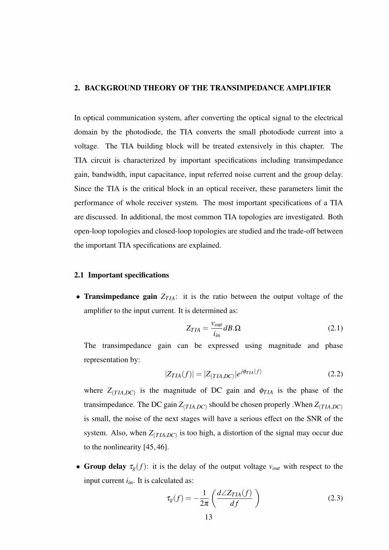
3.1 Cherry Hooper amplifier
The Cherry-Hooper topology was designed to sanction the gain and bandwidth of
an amplifier to be tuned independently of each other. Figure 3.1 shows the simplest
structure of Cherry Hooper topology. It is composed of a transconductance stage gm1
followed by transadmittance stage gm [53]. The first stage converts the input signal to
a current and the second stage with a shunt feedback resistor convert the current ix into
the output voltage.
ix = vingm1 (3.1)
21
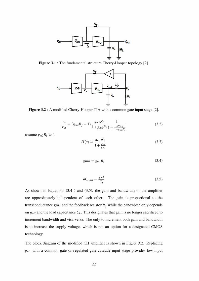
Figure 3.1 : The fundamental structure Cherry-Hooper topology [2].
Figure 3.2 : A modified Cherry-Hooper TIA with a common gate input stage [2].
vo
vin= (gm2R f −1)
gm1Rl
1+gm2Rl
1
1+ sRlCl1+gm2Rl
(3.2)
assume gm2Rl 1
H(s)∼=gm1R1
1+ sClgm2
(3.3)
gain = gm1Rl (3.4)
ω−3dB =gm2
Cl(3.5)
As shown in Equations (3.4 ) and (3.5), the gain and bandwidth of the amplifier
are approximately independent of each other. The gain is proportional to the
transconductance gm1 and the feedback resistor R f while the bandwidth only depends
on gm2 and the load capacitance CL. This designates that gain is no longer sacrificed to
increment bandwidth and visa-versa. The only to increment both gain and bandwidth
is to increase the supply voltage, which is not an option for a designated CMOS
technology.
The block diagram of the modified CH amplifier is shown in Figure 3.2. Replacing
gm1 with a common gate or regulated gate cascade input stage provides low input
22

impedance. That helps avoid the parasitic capacitance from the photodiode. This
configuration leads to enhancement of the amplifier’s gain.
vx = voutRl
Rl +R2(3.6)
vy =−vout
gm(Rl +R2)(3.7)
vy− vx = R f iin (3.8)
ZT =vout
iin= R f (
R1 +R2
R1 +1/gm) (3.9)
assume 1/gm R1
ZT = R f (1+R2
R1) (3.10)
The modified Cherry-Hooper TIA must be frozen as two poles system. The two high
impedance nodes are at Vy and Vout . The output pole is well-defined in Equation (3.11),
while the pole at Vy is determined by Equation (3.12). The quality factor, Q, and the
center frequency of the amplifier are given in Equations (3.13) and (3.14). When Q is
high the modified amplifier offers a wider bandwidth. with more peaking and ringing at
the output. For low Q value it will produce an over damped system. Having Q = 0.707
will deliver the maximally flat response while O = 1/√
3 as designated in [54] will
provide the ideal compromise between peaking and bandwidth.
ωp1 =−1
(R1 +R2)Cl(3.11)
ωp2 =−[1+gm(R1 +R2)]
R fCy) (3.12)
Q =R fCyCL(R1 +R2)(1+gmR1)
R fCy +[CL(R1 +R2)(1+gmR1)](3.13)
The center frequency ω is given by:
ω =
√1+gmR1
R f (R1 +R2)ClCy) (3.14)
23

Figure 3.3 : Capacitive peaking [3].
3.2 Capacitive peaking
Capacitive Peaking technique uses a gain peaking effect of the frequency response by
carefully controlling the capacitance CL loaded at the output node of a preamplifier,
thereby increasing the bandwidth [55–57].
By reanalyzing the feedback preamplifier circuit with the total output capacitance CL
attached, as shown in Figure 3.3, the transfer function can be expressed in second order
form as follows:
ZT =ZT 0ω2
0
s2 + ω0Q s+ω2
0(3.15)
Q =
√ω1ω2
ω1 +ω2(3.16)
ω0 =√
ω1ω2 (3.17)
ω1 =1
RINCT(3.18)
ω2 =1
RoutCL(3.19)
In general, the value of Q ranges from 1/2 to 5/6, which corresponds to the 0−10%
overshoot, for many practical applications for broadening the bandwidth [5]. For
Butterworth response, the maximally flat gain curve is obtained at Q = 0.707. The
bandwidth of the preamplifier can be estimated by setting the magnitude of Equation
(3.15) 0.707 times its low frequency gain ZT 0. That is,∣∣∣∣∣ ZT 0ω20
−ω2−3dB + j
√2ω0ω−3dB +ω2
0
∣∣∣∣∣= 1√2
ZT 0 (3.20)
24

Figure 3.4 : Source degeneration [3, 4].
therefore, ω0 = ω3dB. Thus, once the amount of the required gain peaking (Q) is
determined, the capacitance CL could be easily estimated by Equation (3.16), (3.17)
and (3.18).
3.3 Source degeneration
Another way to broaden the frequency response is to degenerate the input transistors.
The effective transconductance Gm increases at the high frequency to compensate gain
reducing at the cutoff frequency [26, 27, 58].
The capacitor Cs is to bypass the degeneration resistor Rs at high frequencies, providing
the peaking behavior that extends the bandwidth. The RG represents the output
resistance of the preceding stage. Neglecting the body effect, the equivalent transfer
function is given by:
vout
vin= Gm
RD
1+ sRDCL(3.21)
=
(gm(1+ sRsCs)
s2RGCGSRsCs + s(RGCGS +RsCs +RsCGS)+(1+gmRs)
)RD
1+ sRDCL
If the zero at 1/RsCs cancels out the output pole 1/RDCL at the drain, then,
vout
vin=
GmRD
s2RGCGSRsCs + s(RGCGS +RsCs +RsCGS)+(1+gmRs)(3.22)
Assume that the low frequency pole ω1 is much close to the origin, it can be also shown
that,
ω1 =1+gmRs
RGCGS +RsCs +RsCGS≈ 1+gmRs
RsCs(3.23)
25

if RLCGS Rs(Cs +CGS). Hence the input pole frequency is increased by a factor of
(1+ gmRs) implying that the load impedance seen by the preceding stage is reduced.
This has an advantage over a direct trade-off of a gain-bandwidth product without
degeneration.
3.4 Inductive peaking
Inductive characteristics are most important in high-speed applications to enhance the
bandwidth. Oliver Heaviside’s begun used the inductive peaking in 1890s to extend
the bandwidth [59]. The idea of inductive peaking is to use the capacitive load, which
usually limits bandwidth, to resonate with an inductor, thus increasing speed without
additional power dissipation or loss of gain [5], [28] and [29]. Now we will discuss
various forms of inductive peaking circuits with explanation of peaking with poles and
zeros.
3.4.1 Shunt peaking
Shunt peaking is the common technique to expand bandwidth of wide band amplifiers.
It utilizes a resonant peaking at the output of the circuit. It extends the BW by
integrating an inductor to the output load. It introduces a resonant peaking at the
output as the amplitude commences to roll off at high frequencies. At high frequencies
capacitive reactance decreases so the inductor It increments the efficacious load
impedance [60]. Figure 3.5 shows the common source amplifier with shunt peaking
[5, 30].
The transfer function for the shunt-peaking circuit is given by:
vout
vin=−gm
sL+Rs2LC+ sRC+1
=−gmRω0Q
s2 + sω0Q ω2
0ω0Q (3.24)
where,
Q =1R
√LC
(3.25)
ω0 =1√LC
(3.26)
As seen Equation (3.24) can be assumed as a composition of two function that
low-pass function and a band-pass function. In this case, the zero is mainly control
26

Figure 3.5 : Shunt Peaking [3, 5, 6].
Figure 3.6 : Shunt peaking circuit with three poles and two zeros.
the bandwidth improvement and the circuit provides more overshoot than other
second-order configurations. The maximally flat response is obtained when the value
of Q = 0.64, the bandwidth expands by 72%. [61]. By assuming the self capacitance
CL of the inductor, that adds one pole then the circuit has three poles and two- zero [5].
The input impedance is given by:
Z(ω) =R+ jωL−ω2LCLR
jωRC(1−ω2LCL)−ω2L(C+CL)+1(3.27)
= R1−mn( ω
ω0)2 + jm ω
ω0
1−m(1+n)( ω
ω0)2 + j( ω
ω0[1−mn( ω
ω0)2])
where, mR2C , ω0 =1
RC and CL = nC
27

Figure 3.7 : Series Peaking Circuit.
3.4.2 Series peaking
Since the inductive peaking circuits are used mostly as drain load circuit [61]. To
simplify the analysis we can remove the transistor symbol and assume the input current
Ii flowing into the network which is written as :
Ii = ID + IL =Vi
(jωC+
1jωL+R
)(3.28)
The output voltage is:
Vo = ILR =Vi
(1
jωL+R
)(3.29)
So that the transimpedance gain ZT is :
ZT =Vo
Ii=
R−ω2LC+ jωRC+1
(3.30)
Assuming that Ii =1VR and L = mR2C , so that output voltage Vo can be written as:
Vo =1
s2 + smRC + 1
mR2C2
(3.31)
We see that the denominator has two roots. For an efficient peaking the roots should be
complex conjugates. To calculate the cut-off frequency (−3dB frequency), we assume
that the output Vo drops to VODC√2
;
|Vo(ω−3dB)|=σ2
1 +ω21√
σ21 +(ω−3dB +ω1)2)(σ2
1 +(ω−3dB−ω1)2=
1√2
(3.32)
The bandwidth improvement factor η is determined by the ratio between the cut-off
frequency and the maximum non-peaking frequency ωh.
ηb =ω−3dB
ωh(3.33)
28

Figure 3.8 : Series peaking circuit with three poles.
To calculate the input impedance of the circuit:
Zi =1
jωC+1/( jωL+R)=
jωL+R1−2ωLC+ jωRC
(3.34)
The simplified expression of Zi is:
Zi = R1+m( jω
ω0)
1−m( jωω0)2 + jω
ω0
(3.35)
where ω0 =1
RC .
Since when device is connected to the output will have at least some capacitance.
Therefore the series peaking circuit becomes three independent reactive elements
(two capacitors and one inductor), so the circuit has three poles. To have maximum
bandwidth, the value of the input capacitor Ci must be smaller than the loading
capacitance C.
The input impedance is:
Zi =R(1−ω2LC)
(1+ jωRCi)(1−ω2LC)+ jωCL)−ωCR(3.36)
and the output voltage is:
Vo = IiR
(1+ jωR(Ci +C)−ω2LC)+ jω3LRCCi(3.37)
By assuming,
L = mR2(C+Ci)n =C
C+Ciω =
1R(Ci +C)
(3.38)
thereby the transimpedance gain ZT is:
ZT =1
1+ j( ω
ω0)−mn( ω
ω0)2− jmn(1−n) ω
ω0
(3.39)
Since the denominator is a 3rd -order polynomial we have three poles, one of them
should be real and the others two must be complex conjugated. For a series peaking
29

Figure 3.9 : The shunt–series peaking circuit.
circuit the calculation of ω−3dB is relatively easy. The calculation becomes more
difficult, where more poles and sometimes even zeros are introduced. In such cases
it is better to use a computer to calculate response functions.
3.4.3 Shunt–series peaking circuit
Both the shunt and the series peaking can be combined to form a circuit, shown in
Figure 3.9. Here the bandwidth this topology is increased more than the other inductive
topologies [7].
The transimpedance is given by:
ZT (s) =L1
L1L2CCi(s+ R
L1)
s4 + s3 RL1+ s2 L2C+L1Ci+L1C
L1L2CCi+ sR(Ci+C)
L1L2CCi+ 1
L1L2CCi
(3.40)
3.4.4 T-coil peaking technique
T − coil peaking network is shown in Figure 3.10. The circuit uses one transformer
which is bridged by the capacitance Cb [58].The relation R =√
LC must maintain
constant to obtain a constant input impedance Zi = R at any frequency [8].
The inductance L of the center tapped coil can be written as:
L = L1 +L2 +2LM (3.41)
Where L1 and L2 are self inductance and LM is mutual inductance which can be
determined by:
LM = k√
L1L2 (3.42)
In symmetrical case,the values of L1 = L2 case can be determined by:
L1 = L2 =L
2(1+ k)(3.43)
30
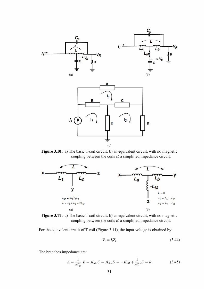
(a) (b)
(c)
Figure 3.10 : a) The basic T-coil circuit. b) an equivalent circuit, with no magneticcoupling between the coils c) a simplified impedance circuit.
(a) (b)
Figure 3.11 : a) The basic T-coil circuit. b) an equivalent circuit, with no magneticcoupling between the coils c) a simplified impedance circuit.
For the equivalent circuit of T-coil (Figure 3.11), the input voltage is obtained by:
Vi = IiZi (3.44)
The branches impedance are:
A =1
sCb,B = sLa,C = sLb,D =−sLM +
1sC
,E = R (3.45)
31

As the result of the hand calculation, we can write the equations of the loop as:Vi00
=
(B+D) x−D −B−B (C+D+E) −CB −C −(A+B+C)
=
I1I2I3
(3.46)
The simplified expression can be written as:
ACD+BDA+BEA+DVA−ECA−E2A−E2B−E2C = 0 (3.47)
Let La = Lb, so that we can rewrite equation as:
sK1 + s−1K2 = 0 (3.48)
where,
K1 =L2
aCb− LLM
Cb−R2LK2 =
LCCb− R2
Cb(3.49)
Assuming both K1 = K2 = 0, so that, we obtain:
L = R2CLM =L4−R2Cb = R2(
C4−Cb) (3.50)
Finally we get the expression of the transimpedance that given by:
ZT =Vo
Ii=
1sC
CA+EA+EB+ECCA+CB+DA+DB+DC+EA+EB+EC
(3.51)
=R
s2R2CCb + sRC/2+1
We see that the denominator has two complex conjugates roots, are given by:
s1,2 = σ1± jω1 =−1
4RCb±
√1
4RCb
2− 1
R2CCb(3.52)
Comparing, the responses for the same kind of poles,the realization show that the -3dB
frequency of the T − coil is exactly twice as much as it is for the two-pole series
peaking circuit and the bandwidth improvement factor is 2.83 [62].
When an input capacitance Ci is connected to the input of the two-pole T − coil, the
circuit becomes has three poles as shown in Figure 3.12.
To simplify the analysis, we assume that the basic two-pole T − coil circuit has a
constant impedance R that unrelated to frequency. So we can determine the transfer
function of the circuit by adding the third pole s3 = 1/RCi to the two-pole network. So
the transimpedance can be written as:
ZT =Vo
Ii=
1(s+ 1
RCi)(s2R2CCb + sRC/2+1)
(3.53)
32

Figure 3.12 : T-coil network with three poles.
For wideband applications, we must have two complex conjugate poles and one real
pole [63]. By adding another inductor between Ci and the T − coil, the bandwidth
can be enhanced by 2.75 times of the two pole T coil circuit. To do that, the coupling
factor k must be improved to be greater than 0.5 [64]. The transfer function of the L+T
network (Figure 3.13) can be determined by multiplication both the transfer functions
of a two-pole series peaking circuit and a two pole T −coil circuit as follows: The two
poles of T-coil section can be expressed as:
s1,2 = σ1± jω1 =−1
4RCb±
√1
4RCb
2− 1
R2CCb(3.54)
and the two poles of section L are written as:
s3,4 = σ3± jω4 =−1
2mRCi±
√1
(2mR2Ci)
2− 1
mR2Ci(3.55)
To obtain better improvement of the bandwidth of L + T configuration, the input
capacitance Ci must be smaller than C. The bandwidth improvement factor η can be
achieved 4.46. Figure 3.14 shows the bandwidth enhancement of different methods.
Curve (a) shows frequency response in the normalization case. Curve (b) represents
the gain peaking of the shunt peaking, curve (c) for the T − coil peaking normalized
frequency, and curve (d) shows the frequency response of the shunt- series peaking
[5, 7].
F(s) =
1mR2C2
i
s2 + smRCi
+ 1mR2Ci
( RR2CCb
s2 + sRCb
+ 1R2CCb
)(3.56)
33

Figure 3.13 : T-coil network with three poles.
Figure 3.14 : The frequency response of the published inductive peakingtechniques [5, 7].
3.4.5 π-type inductor peaking (PIP)
Inductor Peaking (PIP) is an effective bandwidth extension technique. It improves the
bandwidth using several inductors to resonate with the intrinsic capacitance [8].
Figure 3.15 : Small-signal equivalent circuit of the PIP model [8].
34

Figure 3.16 : The normalized frequency response of the inductor peaking (PIP) [9].
Without any inductors, the bandwidth ω0 is limited by the resistive and capacitive
loads. By connecting Ld2 in series with Rd2, the transient current into Rd2 is
delayed and more current is forced to pass to the capacitance load which results an
improvement the bandwidth. In addition, the bandwidth can be further enhanced
by adding Ls1 makes resonance with Cg at higher frequencies. Also adding another
inductor Ld1, Cd and Cg creates resonance at even higher frequencies to get better
enhanced bandwidth.
Figure 3.16 shows the normalized frequency response of the inductor peaking (PIP)
circuit .The bandwidth extension is shown by placing the three peaking inductors one
by one [9].
3.5 Current-mode signaling
When branch currents of the circuit are carriers of the information, the circuit is known
as current-mode circuit. The nodal impedance is low for current-mode circuits and high
for voltage mode networks. Current mode circuits offer an improved bandwidth due to
the following reasons:
• Low nodal impedances decreases time constants of the circuits.
• Low voltage swing reduces the time required to charge and discharge the nodes of
the circuits [65].
35

Figure 3.17 : Distributed amplifiers [10].
In this case, the improvement of the speed is often moderate. At the same time,
decreasing the node impedance increases the node capacitance. Because each node
is assumed to be a first-order RC network that have time constant, τ = RnCn, where Rn
and Cn are the resistance and capacitance of the node.
3.6 Distributed amplification
The bandwidth or speed of a circuit is set by the time constant of the critical node of
the circuit. An effective way to minimize the effect of large shunt capacitance of the
critical node is to break the large shunt capacitor into several smaller shunt capacitors
and separate them with inductors such that the large shunt capacitor is replaced with a
distributed LC network or a transmission line [10, 66].
Shown in Figure 3.17, a common-source amplifier where an shunt peaking inductor is
employed at the drain of the transistor to offset the effect of the large output capacitance
C arising from the large width of the transistor. The equivalent of the original transistor
can be obtained by parallel connecting of N smaller transistors whose width is 1/N.
Inductors is used to separate the transistors and creates two transmission lines, one at
the drain and the other at the source. Resistors R1−4 are used for impedance matching.
36

3.7 Chapter summary
Increasing the bandwidth is critical concern in broadband communications. Several
CMOS TIA technique has been covered. Three topologies, inductive peaking,
current-mode signaling and distributed amplification are the most used to enhance the
bandwidth of circuits.
37

38

4. IMPROVE THE BANDWIDTH OF TRANSIMPEDANCE AMPLIFIERUSING NEGATIVE IMPEDANCE CIRCUIT
This chapter describes a compact Transimpedance amplifier (TIA). Based on the
principle of negative impedance NI circuit, the proposed TIA provides high gain and
wide bandwidth. The schematics and characteristics of negative impedance circuit
NI have been explained. The inductor behavior is synthesized by gyrator C circuit.
The TIA is implemented in 180nm RF MOS transistors in a HV CMOS technology
with 1.8 V supply voltage technology. It reaches −3dB bandwidth of 7 GHz and
transimpedance gain of 54.3 dBΩ in the presence of a 50 f F photodiode capacitance.
The simulated input referred noise current spectral density is 5.9 pA/√
Hz. The power
consumption is 29 mW. The TIA occupies 230µm×45µm of area.
4.1 Introduction
In the receiver of optical communication system, the transimpedance amplifier (TIA)
is the first electrical building block that converts the induced photodiode current
(ipd) into a large voltage signal to be used in the digital processing unit. TIA is
required to have high gain and wide bandwidth at the same time with low power
dissipation. It is well known that, the main challenge to implement wideband TIA
lies in the large photodiode parasitic capacitance at the input node that deteriorate
the performance of the complete receiver system such as speed, sensitivity, and
signal-to-noise ratio. Hence, it is necessary for VLSI designers to improve original
circuit approach in order to reduce the input parasitic effects and to better enhance
the performance in bandwidth, gain, noise, and power consumption [67]. To obtain
high gain, cascode amplifier configuration is not appropriate in low power due to small
voltage swings. Moreover, a multistage amplifiers suffer from stability issue because
of the existence of multiple poles [68]. There are several works that have been reported
to improve the bandwidth of TIA. Inductive peaking has been extensively used to
improve the bandwidth and decrease parasitic capacitance effects [8, 69]. Moreover to
overcome this drawback, a bandwidth enhancement technique using parallel sections
39
of series-peaked stages is described in [70]. However, an extreme size of the inductor
makes the chip large and costly. An inductorless regulated cascode (RGC) topology
reported in [67] decreases the input impedance of the TIA, therefore improving the
bandwidth. Another approach in [71] used several shunt feedback TIAs in parallel in
order to enhance the bandwidth. In that method, there is a strict trade-off between
the number of stages and step-response damping ratio. The effect of the photodiode
capacitance can be more professionally reduced from the bandwidth limitation by
using regulated cascode (RGC) in [72–74]. Furthermore, a negative capacitance circuit
can be used to decrease critical node capacitance to improve the bandwidth of the
amplifier. In this chapter, the design and simulation results of 7GHz transimpedance
amplifier is presented using 180nm CMOS technology. A negative impedance NI
configuration is used as compensation circuit to enhance the frequency response of
the T IA.
This chapter is organized as follows. Section 4.2 and Section 4.3 discuss the basic
principle of negative impedance NI circuit and illustrates a technique to improve
the bandwidth. An implementation of CMOS transimpedance amplifier as a design
example follows in section 4.4. The active inductor is discussed in Section 4.5. The
mathematical model for illustrating the noise of the proposed T IA is introduced in
section 4.6. The simulation results are shown in Section 4.7 and finally conclusions
are summarized in Section 5.7.
4.2 Principle of negative impedance circuit
Merits for using transimpedance amplifier T IA comprise its ability to provide a high
transimpedance gain with wide bandwidth. T IA can be designed as a single ended
voltage amplifier with a feedback resistor RF . Figure 4.1 demonstrates the block
diagram of the proposed transimpedance amplifier T IA. Since a photodiode operates as
current source, it can be replaced by a current source Iin in parallel with the photodiode
capacitance Cpd .
Using Miller effect, if we assume that Rout RF and Rout(Cout +CF) RFCin then, it
can be shown easily that the simplified expression of transimpedance gain ZT is given
40

Figure 4.1 : Block diagram for the traditional resistive feedback TIA with NI circuit.
as:
ZT =Vout
Iin=≈ RF
(1+ sRFCinA )(1+ sRoutCout)
(4.1)
where A is the amplifier gain , RF is the feedback resistor , Cin is the total input
capacitance that includes the photodiode’s capacitance Cpd , the input capacitance of the
amplifier Cg and feedback parasitic capacitance CF(1−A). The output capacitance of
Cout is sum of the amplifier output capacitance and the feedback parasitic capacitance
CF(1− 1/A). The transimpedance gain at low frequencies Zdc equals RF for high
value of A and small value of Rout . As shown in Equation (4.1), the transimpedance
gain function have two real poles p1 and p2 that are given as:
p1,in =A
RFCin(4.2)
p2,out =1
RoutCout
Due to high capacitance of the photodiode capacitance Cpd , the total input capacitance
Cin is larger than the total output capacitance Cout . Besides, feedback resistor RF is
larger than the output resistance Rout . Hence, the dominant pole is suited on the input
node and the output pole can be located at a sufficiently higher frequency than the input
pole. From (4.2), the bandwidth can be improved by increasing the gain (A = gmRout)
and by maintaining the same time constant at the output pole. A better gain A can
be obtained if the output resistance Rout is increased. Increasing Rout can be done by
placing a negative resistance RIN in parallel with the output resistance Rout . In order to
maintain the same time constant at the output node, a negative capacitance can be used.
Increasing the gain A effectively decreases the input resistance and hence increase the
41

frequency of the input pole. As a result, an improvement of the bandwidth can be
obtained.
As shown in Figure 4.1, a first-order amplifier with a negative impedance (NI) circuit
is created at the output node. Both the equivalent output resistance Rout and equivalent
output capacitance Cout are given as:
Rout =RNICRout
RNIC−Rout(4.3)
Cout =Cout−CNIC
Equation (4.3) shows that output capacitance Cout becomes smaller than Cout and the
output resistance Rout becomes greater than Rout . This leads to increase in the voltage
gain A = gmRout , which reduces the input resistance at the input node, while the time
constant at the output node remains approximately the same.
For stability, the pole must be in the left half-plane when choosing the value of RNI to
be larger than Rout and CNI <Cout . NI circuit could be realized by adding active circuit
to output node.
From the point of theory, this technique could be applied at the input node also.
When placing the negative impedance components at the input node, the input resistor
increases and the input capacitance decreases. The large photodiode capacitance still
limits the bandwidth because the value of the negative capacitance does not provide the
effective reduction of the input capacitance to expand the bandwidth. In order to show
the bandwidth improvement, a large value of negative capacitance is required which is
very complex to implement using active devices.
In order to simplify our discussion, the principle of the proposed TIA is explained using
Miller effect as mentioned above. However, to address the fundamental problem of the
TIA design, an alternative analysis can be used. Figure 4.2 shows the small signal
equivalent circuit at high frequencies using single MOS transistor amplifier stage. The
transimpedance gain is given as:
Vout
Iin=
(sRFCin +1−gmRF)Rout
RFRoutx2s2 +(RF(1+gmRout)CF +RoutCout +(RF +Rout)Cin)s+1+gmRout(4.4)
42

Figure 4.2 : Small signal equivalent circuit of TIA.
where x = CFCout +CoutCin +CinCF . For dc case (s = 0), Equation (4.4) can be
simplified as:Vout
Iin=
(gmRF −1)1+gmRout
Rout ≈−RF (4.5)
As shown in Equation (4.4), the circuit contains one zero and two poles. By ignoring
the effect of the zero, fz =1−gmRF
2πRFCF=−gm
CF, which is greater than f−3B [1], the
bandwidth can be approximately given as:
f−3db ≈1
2π
1√RFA Cin(Cout +CF)Rout
(4.6)
where A = gmRout and gm is the transconductance of the amplifier. As seen in Equation
(4.6), in order to boost the bandwidth of the TIA, the gain A should be large during
the design process and the output capacitance should be small. The main goal of using
negative impedance (NI) circuit is increasing the gain A and decreasing the output
capacitance Cout as mentioned previously.
4.3 The negative impedance (NI) circuit
The negative impedance (NI) circuit for single-ended transceiver can be realized with
active devices as shown in Figure 4.3.(a). The circuit consists of NMOS transistor M1
and NMOS transistor M2 in diode configuration. The source of the diode is connected
in series resistance Rs and inductor Ls. The equivalent small signal model of the
negative impedance (NI) circuit is shown in Figure 4.3.(b). The input impedance Zin
is given as:
Zin ≈ Rs + sLs +1
sCgs1+
1gm2 + sCgs2
+gm1
sCgs1
(Rs + sLs +
1gm2 + sCgs2
)(4.7)
where gm1 and gm2 are the transconductance of the transistors and Cgs1 and Cgs2 are the
gate-source capacitances. Better bandwidth improvement can be obtained by inserting
43

Figure 4.3 : (a) Negative impedance (NI) circuit. (b) Small signal equivalent modelof the NI.
series inductor Ls between Cout and CNI . Because it resembles as a third order LC
ladder filter [33]. Equation (4.8), represents the real part of the input impedance.
ReZin ≈ Rs +gm1Ls
Cgs1+
gm2
g2m2 +ω2C2
gs2−
gm1(Cgs2/Cgs1)
g2m2 +ω2C2
gs2(4.8)
As pointed out in (4.8), to obtain a negative resistance, the total value of ReZin
should be negative. The value of the negative resistance is limited by the size of the
transistors, the series inductor Ls and the series resistor Rs . The imaginary part of the
input impedance of ImZin can be expressed as:
ImZin ≈ ωLs−1
ωCgs1− gm1Rs
ωCgs1−
ωCgs2
g2m2 +ω2C2
gs2−
gm1gm2/(ωCgs1)
g2m2 +ω2C2
gs2(4.9)
Assuming that both transistors have identical transconductance (gm1 = gm2) ,
ω2LsCgs1 < 1 and ω2C2gs < g2
m, then ImZin can be simplified as:
ImZin ≈ −1
ωCgs1(ωLsCgs1−gm1Rs)<
1ωCgs1
(4.10)
Figure 4.4 and 4.5 show the plots of the real and the imaginary components of the
negative impedance NI circuit. From the simulation results, we see that the real part
represents a negative resistance that varies with the frequency. The NI circuit provides
an enough negative resistance at frequencies up to7 GHz. The imaginary component
acts as a negative capacitance.
Figure 4.6 illustrates the variation of the capacitance value over the frequency
capacitance value at the frequency of 7 GHz as −5 f F .
44

Figure 4.4 : The real component of the input impedance of ZNI .
Figure 4.5 : The imaginary component of the input impedance of ZNI .
4.4 Configuration of the proposed TIA with negative impedance NI circuit
The simplified diagram of the proposed transimpedance amplifier (T IA) is shown in
Figure 4.7. It is a single-ended design including NMOS transistor Mx, feedback resistor
RF connecting the output to the input in order to decrease the dominant effect of the
input pole, and negative impedance (NI) circuit. The output of TIA is taken at the drain
of transistor Mx. In the proposed TIA, between the drain capacitance of Mx and the gate
capacitance of M1, a small series inductor L1 can improve the bandwidth further.
45
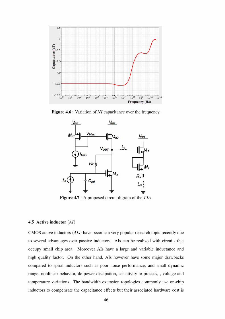
Figure 4.6 : Variation of NI capacitance over the frequency.
Figure 4.7 : A proposed circuit digram of the T IA.
4.5 Active inductor (AI)
CMOS active inductors (AIs) have become a very popular research topic recently due
to several advantages over passive inductors. AIs can be realized with circuits that
occupy small chip area. Moreover AIs have a large and variable inductance and
high quality factor. On the other hand, AIs however have some major drawbacks
compared to spiral inductors such as poor noise performance, and small dynamic
range, nonlinear behavior, dc power dissipation, sensitivity to process, , voltage and
temperature variations. The bandwidth extension topologies commonly use on-chip
inductors to compensate the capacitance effects but their associated hardware cost is
46

very high. As a result, decreasing the area of required inductors for a TIA design is
very important. Most AIs reported in [75–79] were based on the knowledge of gyrator
C topology. As we need to design a floating active inductors to implement the negative
admittance circuit (NI), the architecture of active inductors in [80, 81] could be used
to obtain several nH of inductance operating at a few GHz region as shown in Figure
4.8. The gyrator is implemented by connection of two differential transconductance
amplifiers back to back. The cross coupled NMOS transistors M7 and M8 provide a
negative resistance to reducing the total series resistance of the active inductor network
which provides a high quality factor Q of the active inductor. For simplicity, the circuit
can be separated into two identical half-circuit. Figure 4.9(a) displays the small-signal
equivalent circuit of half-circuit [82]. The input impedance can by simplified as:
Figure 4.8 : Circuit schematic of floating active inductor.
Zin ≈ 2g2 + sC2
s2C1C2 + s(g1C2 + s(g1C2 +g2C1))+gm1gm2g1g2(4.11)
where C1 and C2 are the total capacitance of the drain nodes, g1 and g2 are the total
conductance at the drain nodes [82].
Figure 4.9(b) shows the simplified model of the active inductor. The elements value L,
R, G, and C can be calculated thus:
L =2C2
gm1gm2,L =
2g2
gm1gm2,G =
g1
2,C =
C1
2(4.12)
47

Figure 4.9 : (a) equivalent small-signal of half-circuit of Floating active inductor (b)Simplified model of active inductor.
Equation (4.12) shows that the desired inductance value can be obtained by decreasing
gm1 and gm2 or increasing C2.
4.6 Noise analysis of the proposed transimpedance amplifier
The proper characterization of noise of the T IA is important for the receiver due to the
small current of the photodiode. Replacing the passive inductors by active elements
produce some noise in the response of the proposed T IA. So, in order to operate at
high sensitivity, the noise level must be very small [83]. The main noise sources of the
TIA are the thermal noise of the resistor, the noise of MOS transistor and the flicker
that can be neglected because it is not dominant.
Figure 4.10 : (a) Noise model of MOS transistor, (b) Noise model of a resistor.
Both the transistor and resistor noise models are shown in Figure 4.10, where ¯v2ng =
¯i2ndg2
m.
Both noises sources of the gate and the source can be modeled by shunt current
source with noise powers of ¯i2ng = 4kBT δ∆ f (ω2C2gs/5gd0) and ¯i2nd = 4kBT γgd0∆ f ,
respectively, where T is the temperature (Kelvin) , γ is the bias dependent factor, kB
is the Boltzmann’s constant (Joule/Kelvin), Cgs is the gate-source capacitance, δ is the
gate noise factor and gd0 is the zero bias of transconductance of the transistor [84,85].
48

From the T IA circuit in Figure 4.7, the equivalent input referred current noise of Mx is
given as:¯i2ngx = 2qkBIGx +ω
2C2gsx
¯v2ngx (4.13)
where q is the electron charge, IGx is the gate induced current that can be neglected and
v2ngx is given as:
¯v2ngx =
¯i2ngx
g2mx
=
¯i2RF + ¯i2nx +¯i2ngL1 +
¯v2ng− ¯v2
ngxR + ¯i2nL1
g2mx
(4.14)
where ¯i2nL1 is the equivalent input noise of active inductor L1. The simplified expression
of the equivalent input noise of active inductor L1 can be written as:
¯i2nL1 =¯i2ng +
¯i2dn +¯i2d p +2g2
mp¯v2gp +g2
mnZ2gn2 ¯i2gn +2 ¯i2dn +2 ¯i2d p +2g2
mp¯v2gp (4.15)
=2 ¯i2gn(1+g2mnZ2
gn)+2 ¯i2dn(1+g2mnZ2
gn)+2 ¯i2d p(1+g2mnZ2
gn)
+4g4mn
¯v2gnZ2
gn +2g2mp
¯v2gp(1+g2
gmnZ2gn)
Note that Z2gn =
1ω2C2
gn[86], then the input noise of serial active inductor ¯i2nLs is derived
as:
¯i2nL1 = 8kBT ∆ f
(1+
g2mn
ω2C2gsn
)(δn
ω2C2gsn
5gd0n+ γngd0n + γpgd0p +δp
g2mp
5gd0p
)(4.16)
+8kBT ∆ f δpg4
mn5gd0pω2C2
gsn.
then total input noise ¯i2in,total becomes:
¯i2in,total =¯i2n f +
¯i2nL1 +
(1
R2f+ω
2C2in
)¯v2ngx (4.17)
where ¯i2n f is the thermal noise of diode resistance R f which is given by:
¯i2n f =4kBT
R f(4.18)
Substituting Equations (4.14), (4.15), (4.16) and (4.18) into Equation (4.17), the
simplified expression of total input noise ¯i2in,total can be written as:
¯i2in,total ≈4kBT
R f+
1g2
mx
(1
R2f+ω
2C2in
)(4.19)
4kBTRF
+ kBT γgd0∆ f +4kBT δ∆ fω2C2
gs
5gd0+8kBT ∆ f
(1+
g2mn
ω2C2gsn
)(
δnω2C2
gs
5gd0n+ γngd0 + γpgd0p +δp
g2mp
5gd0f
ω2C2gs
5gd0
)+8kBT δp∆ f
g4mn
5gd0ω2C2gsn
49

As seen in Equation (4.19), the total noise can be minimized by choosing RF and gmx
to be as large as possible. Improving gmx can be done by increasing bias current or
expanding the aspect ratio W/L of the transistor. High power consumption is induced
when bias current increases. Moreover, using a large transistor aspect ratio increases
the capacitance Cgs and Cgsn which generates more noise. As a result, we have to select
the proper ratio W/L and bias current to optimize the noise performance.
4.7 Simulation results
In order to evaluate the performance of the proposed T IA as shown in Figure 4.11,
the T IA was implemented using 180 nm RF MOS transistors in a HV CMOS process
technology. All post layout simulation results have been performed by using cadence
software tools.
Figure 4.11 : TIA realization.
Figure 4.12 shows the simulated transimpedance gain versus frequency for 50 f F
photodiode capacitance for the proposed TIA with and without the negative impedance
NI circuit. The proposed TIA with NI is described as having a transimpedance gain of
54.3 dBΩ and bandwidth of 7 GHz. The simulation results shows that the bandwidth
is improved by 6 GHz compared to the TIA without negative impedance NI circuit
and without scarifying the gain. As a result, the overall bandwidth of the TIA with
NI is extended 7 times more. Simulations resulted in considerable increase of gain
50

bandwidth product (GBP) by a factor of 5. The T IA consumes 29 mW from 1.8 V
supply.
Figure 4.12 : Simulation results comparison of the frequency response of TIA withand without NI.
Figure 4.13 shows the frequency response of the T IA for different photodiode
capacitances varying from 50 f F to 200 f F . For photodiode capacitance 200 f F , the
−3dB bandwidth is above 2.5 GHz and it is above 3.5 GHz with a value of photodiode
capacitance 100 f F .
Figure 4.13 : Frequency response of the proposed TIA for four different values ofCpd .
Figure 4.14 illustrates the simulation of input noise current spectral density. Simulation
results shows an equivalent input noise current spectral density below 5.9 pA/√
Hz
51
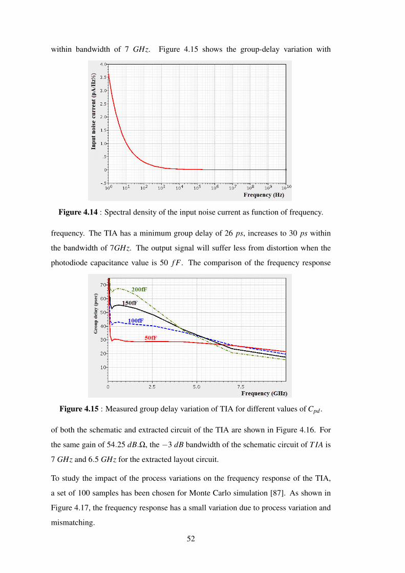
within bandwidth of 7 GHz. Figure 4.15 shows the group-delay variation with
Figure 4.14 : Spectral density of the input noise current as function of frequency.
frequency. The TIA has a minimum group delay of 26 ps, increases to 30 ps within
the bandwidth of 7GHz. The output signal will suffer less from distortion when the
photodiode capacitance value is 50 f F . The comparison of the frequency response
Figure 4.15 : Measured group delay variation of TIA for different values of Cpd .
of both the schematic and extracted circuit of the TIA are shown in Figure 4.16. For
the same gain of 54.25 dB.Ω, the −3 dB bandwidth of the schematic circuit of T IA is
7 GHz and 6.5 GHz for the extracted layout circuit.
To study the impact of the process variations on the frequency response of the TIA,
a set of 100 samples has been chosen for Monte Carlo simulation [87]. As shown in
Figure 4.17, the frequency response has a small variation due to process variation and
mismatching.
52

Figure 4.16 : The frequency response of the TIA (schematic and extracted).
Figure 4.17 : Monte Carlo simulation results for the frequency response for 100samples.
Corner analysis is used to make the design more realistic by simulating the circuit in
different operational conductions, such as different temperatures and altered process
corners. Figure 4.18 shows the transient response of the TIA at different process
corners for 10µA(p−p). As a result, the merits of proposed TIA shows that the TIA
can work normally at different process corners with a small input current for wide
bandwidth. Figure 4.19 shows layout of the TIA. The occupied area of the layout is
230µm×43µm.
Table 4.1 shows a comparison of the proposed TIA performance with other works.
From Table 4.1, it can be seen that the noise of the proposed TIA is smaller than
53

Figure 4.18 : Transient response of the TIA under different corners.
Figure 4.19 : Layout of the TIA.
Table 4.1 : Performance Comparison of Recent CMOS TIAs.
Cpd Gain BW Power NoiseRef. ( f F) (dBΩ) (GHz) (mW ) (pA/
√Hz) Area
This work a 50 54.3 7 29 5.9 230µm×45µm[88] a 50 54.3 5.35 3.5 8.2 ——[8] b 50 51 30.5 60.1 34.3 1.17mm×0.46mm
[89] b – 60 6.9 16.9 – 0.051mm2
[90] b – 50 7.5 4.1 – 42mm×0.17mm[91] a – 51.7 8.5 14 – –[92] a 200 64.8 4.5 3.5 13.7 97µm×53µm
a: Simulation results, b: Measurement results
the other TIA configurations, where the active inductors have been used. The power
consumption is comparatively higher than the other TIA circuits.
4.8 Conclusion
This paper presents a compact transimpedance amplifier T IA. The effects of using the
negative impedance NI circuit are demonstrated through a proposed transimpedance
54

amplifier. The TIA is implemented in 180 nm RF MOS transistors in a HV CMOS
technology with 1.8 V supply voltage technology. Cadence tools is used in analyzing
the performance of the T IA. It is observed that the T IA provides -3dB bandwidth
at 7 GHz, transimpedance gain of 54.3 dB.Ω in the presence of a 50 fF photodiode
capacitance and input referred noise current spectral density of 5.9pA/√
Hz . The
power consumption is 29 mW . The TIA occupies 230µm×45µm of area. Simulation
results show that the TIA is very proficient for applications in optical transceivers.
55

56

5. IMPROVE THE BANDWIDTH OF TRANSIMPEDANCE AMPLIFIERUSING MATCHING TECHNIQUE
This chapter describes a matching technique to improve the bandwidth of multi-GHz
frequency ranges for the transimpedance amplifier. It is shown that by simultaneously
using of series input matching topology and T-output matching network, the bandwidth
of the TIA can be obviously improved. This methodology is supported by a design
example in a 0.18 µm CMOS technology. The post layout simulation results show a
-3dB bandwidth of 20 GHz with 50 f F photodiode capacitance, a transimpedance gain
of 52.6 dBΩ, 11 pA/√
Hz input referred noise and group delay less than 8.3 ps. The
TIA dissipates 1.3 mW from a 1.8 V supply voltage.
5.1 Introduction
The continuous growth in the commercial wireless telecommunications market has
been driving to satisfy the demands of high speed, low cost and high integration of
radio-frequency (RF) broad-band receivers [93]. Recently, it is reported that, every
ten years, the speed of analog CMOS circuits increases by one order of magnitude.
Moreover, the integration and cost advantages of CMOS technologies encouraged
extensive work on developing the optical communication system [94].
One of the main challenges in the receiver system is the design of a wideband
transimpedance amplifier TIA. In CMOS technology, common source (CS) and
common gate (CG) are the most used transistor configurations in TIA topologies. CS
TIA has high gain and superior good noise performance. CG configuration provides
low power, less parasitic stable circuit, and less noise performance [92, 95, 96].
Furthermore, the inductive source degenerated technique is used to improve both the
gain and noise performance of TIA [97].
The input matching mechanism is conceivable for CG configuration so that, it
is extensively used in wideband TIA circuits [98, 99]. On the other hand, CS
configuration may be used in wideband TIAs using feedback network or matching
circuits.
57

Cascode stage is generally used in CMOS RF circuits. It composes of a CS stage
followed by a CG stage. Cascode configuration provides high power gain, better
noise performance and low power consumption [100]. For low frequencies, the noise
sources of the upper transistor is degenerated by the output impedance of the lower
transistor. Therefore cascode stage configuration has better noise performance. In
high frequencies, the admittance parasitic of common node (drain-source) increases as
frequency increases. As a result, when the source impedance of upper transistor is low,
its drain noise performs in the output [95,101]. It is possible to improve the bandwidth
of cascode stage using feedback technique [102, 103] and matching networks [104].
In this chapter, a matching technique is applied to improve the bandwidth of the
transimpedance amplifier based on using cascode topology. The rest of this paper
is organized as follows: Section 5.2 demonstrates the proposed TIA design. The
matching technique to improve bandwidth is presented in Section 5.3 and Section 5.4.
The noise analysis is discussed in Section 5.5. To demonstrate the practicality of this
technique, the simulation results of a design example is followed in Section 5.6.
5.2 The proposed TIA design
Applying proper matching networks at the input and the output nodes are the strategic
phases in improving the bandwidth of the TIA. For cascode topology, the input
impedance is pure capacitive (in very low frequencies) so that a resistive part must
be added to the input impedance. That can be done by connecting a degenerating
inductance in the source of CS transistor. On the other hand, CG configuration offers
wideband matching possibility.
It has been explored that combination of CS configuration in the first stage and cascode
configuration in the second stage provides good noise performance of CS stage and
high gain of cascode stage [105, 106]. The noise is small because of capacitances
and parasitic admittances existence at the cascode node. So that, the best topology of
the proposed TIA design is cascading stages of CS cascode configuration as shown in
Figure 5.1. Both the input and output matching techniques will be explained in the
next sections.
58

Figure 5.1 : Schematic of proposed TIA with matching networks.
5.3 Input matching analysis
There are different topologies which could be used to implement the input matching.
Probably the simplest matching network is using a series inductor at the gate of the
input transistor as shown in Figure 5.1. Figure 5.2 shows the small signal model of the
input matching circuit. Neglecting the effect of the feedback capacitance Cgd1 of the
input transistor M1 and the drain-source conductance go1, The input impedance Zing1
can be represented as the parallel of a resistance Rp with the capacitor Cgs. Thus, the
small signal model to calculate the input impedance Zin has to be redrawn as shown in
Figure 5.3.
Figure 5.2 : Small signal model of the input matching of Figure 5.1.
Figure 5.3 : Simplified small signal model to calculate of Zin.
59

The input impedance Zin is given by:
Zin =Rp
1+ω2R2pC2
T(5.1)
+ jω
(Lg−R2
pCT (1−ω2LgCT )
1+ω2R2pC2
T
)
where Ls is the degeneration inductor at the source of M1 and gm1 is the
transconductance of transistor M1. Both of Rp and CT are given by:
Rp =1
ω2LsCgs1gm1(5.2)
CT =Cgs1 +Cgb
In order to realize a conjugate matching of the transimpdance amplifier , the real part
of ReZin must be equal the diode resistance RD and the imaginary competent of
ImZin have to be complex conjugate of photodiode impedance Xs. That means :
RD =Rp
1+ω2R2pC2
T, (5.3)
−ω
(Lg−R2
pCT (1−ω2LgCT )
1+ω2R2pC2
T
)=
1ωCpd
where Cpd is the photodiode capacitance .
From Equation (5.3), matching conductions can be satisfied by using the proper values
of the inductances Ls and Lg. Supposing that ω2R2pC2
T 1, then Ls can be given by:
Ls =RD
ω
(CT
Cgs1
),Lg =
1Cpd
+ 1Cgs1
ωRDg2m1
(5.4)
where ω is cut- off frequency.
5.4 Output matching analysis
As shown in Figure 5.4, we choose the T configuration to implement the output
matching. In order to calculate the output impedance Zout , first of all, we have to
determine the admittance Yins2 at the source of M2. From the small signal circuit shown
in Figure 5.4(a), we have:
Yins2 = Ydb2−(gm2 +go2)(Cgs2go2 +Cgd2Yss2)
Yss2Cgs2(5.5)
+(gm2 +go2)Cgd2
Cgs2+( jωCgd2 +go2)
60

where, Yss2 =Ys2+Ysb2+ jωCgs2+gm2+go2 , Ys2 is the load at the source of transistor
M2 that given by (Ys2 = Ysb2 +Yind1) , and Ysb2 is source-substrate admittance of M2 ,
Ydb2 is drain-substrate admittance of M2 and Yind1 is the input admittance to the drain
of M1.
Yind1 =Ydb1 +jω(Cgs1go1 +Cgd1Yss1)
jωCgs1(− jωCgs1−gm1)+Yss1Ygg1(5.6)
×(− jωCgd1 +gm1−
(gm1 +go1)Ygg1
jωCgs1
)+( jωCgd1 +go1)(gm1 +go1)
Cgd1
Cgs1
where Yss1 = Ys1 +Ysb1 + jωCgs1 +gm1 +go1 and Ygg1 =Yg1
1+RgYg1+ jωCgd1 + jωCgs1.
Yg1 is the input admittance at the gate transistor M1, and Ys1 is the load at the source of
M1 which is given by : Ys1 = Ysb+ generation admittance at the source of M′1".
Figure 5.4 : (a) The small signal model to calculate Zout (b) The small signalmodel to calculate Yind1′ at drain of M′1.
61
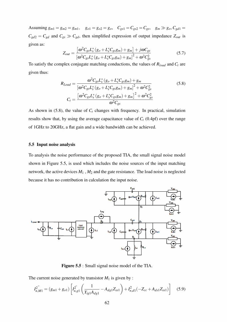
Assuming gm1 = gm2 = gm1, go1 = go2 = go, Cgs1 =Cgs2 =Cgs, gm go, Cgd1 =
Cgd2 = Cgd and Cgs Cgd , then simplified expression of output impedance Zout is
given as:
Zout =
[ω2CgsL∗s (go +L∗sCgsgm)+gm
]+ jωCgs
[ω2CgsL∗s (go +L∗sCgsgm)+gm]2+ω2C2
gs
(5.7)
To satisfy the complex conjugate matching conductions, the values of Rload and Ct are
given thus:
RLoad =ω2CgsL∗s (go +L∗sCgsgm)+gm
[ω2CgsL∗s (go +L∗sCgsgm)+gm]2+ω2C2
gs
(5.8)
Ct =
[ω2CgsL∗s (go +L∗sCgsgm)+gm
]2+ω2C2
gs
ω2Cgs
As shown in (5.8), the value of Ct changes with frequency. In practical, simulation
results show that, by using the average capacitance value of Ct (0.4pf) over the range
of 1GHz to 20GHz, a flat gain and a wide bandwidth can be achieved.
5.5 Input noise analysis
To analysis the noise performance of the proposed TIA, the small signal noise model
shown in Figure 5.5, is used which includes the noise sources of the input matching
network, the active devices M1 , M2 and the gate resistance. The load noise is neglected
because it has no contribution in calculation the input noise.
Figure 5.5 : Small signal noise model of the TIA.
The current noise generated by transistor M1 is given by :
¯I2n,M1 = (gm1 +go1)
[¯I2
n,g1
(1
Yig1Adg1−Adg1Zss1
)+ I2
n,d1(−Zcc +Ads1Zss1)
](5.9)
62

where ¯I2n,g1 is the gate noise of M1 and is given by [107]:
¯I2n,g1 = 4kBT δgg, δ = 4/3 and gg =
ω2Cgs1
5gd0(5.10)
where gg is the equivalent conductance at the gate , gd0 is the drain-source conductance
when Vds = 0 , and δ is bias dependent noise factor.
Yig1 is the admittance of gate node of M1 and is given by :
Yig1 =(1+RgYinm)(1+RgYing1)
Yinm(1−RgYing1)+Ying1(1+RgYinm)(5.11)
Yinm is the input admittance of the input matching circuit. Adg1 is the transfer function
between the drain and gate of M1. It is calculated as:
Adg1 =(gm1 +go1)(gm1 + jωCgs1)−Yss1(gm1− jωCgd1)
Yss1Ydd1−go1(gm1 +go1)(5.12)
where,
Yss1 = gm1 + jωCgs1 +go1 +Ys1 +Ysb1
Ydd1 = go1 + jωCgd1 +Yd1 +Ydb1
Yds1 is the transfer function between the drain and source of M1 . It is calculated as :
Ads1 =ygg1(gm1 +go1)+ jωCgs1( jωCgd1−gm1)
jω(gm1−go1)+Ygg1Ydd1(5.13)
where Ygg1 = jωCgs1 + jωCgd1 +Yg1
1+RgYg1Yg1 is the equivalent admittance of the input
matching circuit at the gate node of M1. Zss1 is the nodal impedance of the source of
M1 and is calculated as :
Zss1 =1
Yins1 +1
ωLs( j+1/QLs)
(5.14)
where Yins1 is the equivalent admittance at the source node of M1 and is given by:
Yins1 =jωCgd1x+ jωCgs1Yddx+Ygggo1(gm1 +go1)+
Cgs1Cgd1
go1YggYdd
jωCgd1( jωCgs1−gm1)−YddYgg +Cgs1Cgd1
go1 +Yss(5.15)
where
Ygg =Yg1 + jωCgs1 + jωgo1
Yss =go1 + jωCgs1 +gm1 +Ysb1
Ydd =go1 + jωCgd1 +Yd1 +Ydb1
63

Zcc is the equivalent admittance at cascode and is given by:
Zcc =1
Yind1 +Yins2(5.16)
both Yind1 and Yins2 are calculated by using equation (5.6) and equation (5.5).
The current noise generated by transistor M2 is given by :
¯I2n,M2 = (gm1 +go1)
(− ¯I2
n,g2 +¯I2
n,g2
)Zcc− ¯I2
n,d2 (5.17)
The noise outcome by gate resistor ¯I2n,ORg is given by:
¯I2n,ORg = (gm1 +go1)×
(Zing1Adg1−Zgg1Agi1Agdi1
)¯In,Rg (5.18)
where, Zing1 is the impedance at the gate of M1 . Adgi1 is the transfer function between
the drain and gate of M1 and Agi1 can be determine by Agi1 = 1−Ying1Rg .
The input matching network is modeled by two port noise model with two current
noise sources ¯I2n,1 and ¯I2
n,2 , where,
I2n,1 = 4kBT ∆ f
(RLg
RLg +Rs + jωLg +1
jωCpd
)(5.19)
I2n,2 = 0
Hence current noise generated by input matching network is given by :
¯I2n,m = (gm1 +go1)
(¯I2n,1Zii1Ainm1Aig1Adg1
)(5.20)
where Zii is the equivalent input impedance, Ainm is the transfer function of the input
matching circuit. Finally, the total input current noise is given by:
¯I2n,total =
¯I2n,M1 +
¯I2n,M2 +
¯I2n,ORg +
¯I2n,m (5.21)
5.6 Design example and simulation results
To demonstrate the effectiveness of the matching methodology, a design example was
implemented using 0.18 µm HV CMOS process. Simulations are done with a single
supply (i.e.1.8V) and the presence of a 50 f F photodiode capacitance. As shown in in
Figure 5.6, the frequency response of the provides a transimpdance gain of 53.7 dBΩ
and bandwidth range of 1 KHz−15 GHz for schematic circuit and 20 GHz bandwidth
64

Figure 5.6 : The frequency response for Cpd = 50 f F .
with 52.6 dBΩtransimpedance gain for the extracted TIA. The power consumption is
in the range of 1.3 mW .
Figure 5.7 shows the frequency response against the input capacitance Cpd . For the
photodiode capacitance of 100 f F , the gain is 55 dBΩ and bandwidth is 4.5 GHz
and it is above 3 GHz for Cpd = 200 f F with gain of 57 dBΩ. For large value of
photodiode capacitance 500 f F , the gain becomes 61 dBΩ and 400 MHz bandwidth.
Figure 5.7 : The frequency response for different values of Cpd .
The simulation of input noise current spectral density against the input capacitance Cpd
is depicted in Figure 5.8. It shows that the noise is maximum at low frequencies then
it decreases at high frequencies over the desired bandwidth. The average input noise
of the TIA is 11 pA/√
Hz for input capacitance Cpd = 50 f F and 38 pA/√
Hz when
Cpd = 500 f F .
The group-delay variation is a significant parameter of a TIA. Even with large enough
bandwidth, distortions of the output may take place if the phase linearity of the TIA
65

Figure 5.8 : The input noise current spectral density against the photodiodecapacitance Cpd .
is insufficient. It can be observed in Figure 5.9, within the bandwidth of 20 GHz, the
TIA circuit has a group delay variation of less than 8.3 ps when Cpd = 50 f F .
Figure 5.9 : The group delay variation of the TIA.
To study the impact of the process variations on the frequency response of the TIA,
a set of 100 samples has been chosen for Monte Carlo simulation. As shown in
Figure 5.10, the frequency response has a small variation due to process variation and
mismatching.
Corner analysis is used to make the design more realistic by simulating the circuit in
different operational conductions, such as different temperatures and altered process
corners. Figure 5.11 shows the transient response of the TIA at different process
corners for 10µA(p−p). As a result, the merits of proposed TIA shows that the TIA
can work normally at different process corners with a small input current for wide
bandwidth.
66
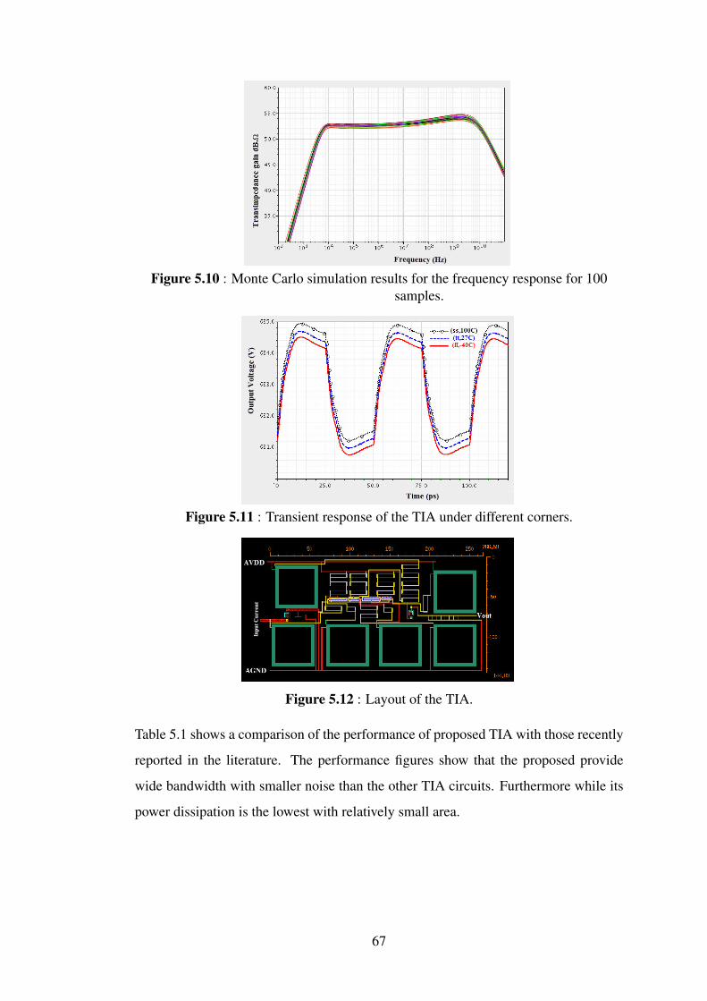
Figure 5.10 : Monte Carlo simulation results for the frequency response for 100samples.
Figure 5.11 : Transient response of the TIA under different corners.
Figure 5.12 : Layout of the TIA.
Table 5.1 shows a comparison of the performance of proposed TIA with those recently
reported in the literature. The performance figures show that the proposed provide
wide bandwidth with smaller noise than the other TIA circuits. Furthermore while its
power dissipation is the lowest with relatively small area.
67

Table 5.1 : Performance Comparison of Recent CMOS TIAs.
Cpd Gain BW Power Noise Group dealyRef. ( f F) (dBΩ) (GHz) (mW ) (pA/
√Hz) (ps) Area
This worka 50 52.6 20 1.3 11 8.3 140µm×266µm[92]b 200 64.8 4.5 3.5 13.7 — 97µm×53µm[89]b — 60 6.9 16.9 — — 0.051mm2
[90]a — 50 7.5 4.1 — — 42mm×0.17mm[91]a — 51.7 8.5 14 — —
[108]a 50 54.3 7 29 5.9 26 230µm×45µm[88]a 50 54.3 5.35 3.48 8.2 — —[8]b 50 51 30.5 60.1 34.3 — 1.17mm×0.46mm
a: Simulation results, b: Measurement results
5.7 Conclusion
This work demonstrates the performance of a transimpedance amplifier TIA using
matching networks technique with cascode configuration. The proposed TIA provides
wide bandwidth and low noise. The TIA is designed in a 0.18 µ m CMOS technology.
The post layout simulation results shows that the proposed TIA achieves a bandwidth
performance of 20 GHz, 52.6 dB.Ω transimpedance gain, 11 pA/√
Hz input referred
noise and a group variation of less than 8.3 ps within the pass band. The power
dissipation is 1.3 mW from a 1.8 V supply voltage.
68
6. IMPROVE THE BANDWIDTH OF TRANSIMPEDANCE AMPLIFIER BYMODIFICATION THE INPUT CIRCUIT
We present a new transimpedance amplifier (TIA) design possessing an improved
bandwidth. This TIA employs a parallel combination of two series resonate circuits
with different resonate frequencies on the conventional regulated common gate (RGC)
architecture. In the proposed TIA, we employ the capacitance degeneration and series
inductive peaking for pole-zero elimination. We implemented the layout of proposed
TIA in a 0.18 µm CMOS process, where a 100 f F photodiode is considered. Our
post-simulation test results show that the TIA provides 53 dBΩ transimpedance gain
and 24 pA/√
Hz input referred noise. The designed TIA consumes 11 mW from a
1.8 V supply, and its group-delay variation is 5 ps over 13 GHz3−dB bandwidth.
6.1 Introduction
Continuous growth in the wireless telecommunication has evolved to high level of
chip integration and focused research studies towards the field of high frequency
applications [109]. The accelerated CMOS technology is the only candidate that can
satisfy the demands for low-cost and high integration with reasonable speed for analog
applications in the Giga-Hertz range [110].
The transimpedance amplifier (TIA) is the critical block in the optical communication
system that converts the induced photodiode current into an amplified voltage signal to
be used in the digital processing unit. The bandwidth is considered as the highest
priority in TIA design. The challenge in TIA design lies in the large photodiode
parasitic capacitance Cpd , the input node that degrades the performances of the TIA.
Therefore, it is required to decrease the input parasitic effects and prior to focusing on
the compromise between the bandwidth and the noise [67].
There have been two commonly used topologies in designing wideband CMOS TIAs:
the common gate (CG) amplifier and the shunt feedback amplifier [48]. Several
bandwidth enhancement efforts have been reported in published literature which were
69

based on isolation of the input capacitance of the photodiode to minimize its effect on
the bandwidth calculation. Inductive peaking is one of the commonly used techniques
to improve the bandwidth and decrease parasitic capacitance effects [111]. Placing
an inductor in a strategic location of the amplifier circuit provides a resonance with
parasitic capacitances, which expands the bandwidth of the TIA [5,28,29]. Capacitive
peaking has been used for bandwidth extension by using a capacitor to control the pole
locations of a feedback amplifier [56,112]. Multiple shunt parallel feedback is another
approach for enhancing the bandwidth [71]. The effect of the photodiode capacitance
can be more professionally reduced from the bandwidth limitation by using regulated
cascode (RGC) [67]. In this chapter, we have propose a new TIA design with
improved bandwidth. The proposed TIA is based on modification of the input part
of the conventional RGC TIA architecture by using parallel arrangement of two series
resonate circuits with different resonate frequencies. Capacitance degeneration and
series inductive peaking networks are used for pole-zero elimination to improve the
bandwidth.
The paper is organized as follows: in Section 6.2, we present an overview of the
traditional RCG input stage and we introduce the concept of modified RCG input
stage and the analysis of the architecture of parallel arrangement of two series resonate
circuits with different resonate frequencies. We present the capacitance degeneration
architecture and proposed TIA design in Section 6.3 and Section 6.4, respectively. We
present the noise analysis in Section 6.5, demonstrative simulation results in Section
6.6, and the conclusions in Section 6.7.
6.2 Regulated common gate (RCG) input stage
6.2.1 Conventional RCG input stage
Among all the building blocks in an optical communication system, the TIA is the one
of the most critical blocks in receiver design. It is a well-known fact that RGC input
configuration can attain better isolation within the large photodiode capacitance Cpd by
local feedback topology. Figure 6.1 shows the schematic diagram of the conventional
RGC with a PD, which converts the incoming optical signal to a small signal current
Ipd . The common-source (CS) amplifier consists of M1 and RD operates as a local
70

feedback technique and regulates the CG. As a result of the small-signal analysis, the
input resistance of the RGC circuit is given by [113, 114].
Zi,RCG =1
gm2(1+gm1RD), (6.1)
where gm1 and gm2 are the transconductance of M1 and M2 respectively. It is
clearly seen that the input resistance decreased because the transconductance Gm is
(1+gm1RD) times larger than that of CG amplifier input stage, where (1+gm1RD) is
the DC gain of the local feedback. Therefore, RGC stage acts as a buffer between the
PD and the TIA stage and decreases the effect of the photodiode capacitance Cpd [114].
Figure 6.1 : Regulated common gate (RCG) TIA.
6.2.2 Modified RCG input stage
In the design of ultra-wideband TIAs, the wideband input stage plays very critical
role. The design methodology of the narrow-band TIA is our first focus followed by
demonstration of how to extend its input bandwidth.
Figure 6.2 : The input part of a narrow band RCG TIA.
Figure 6.2 shows the input part of a typical narrow band TIA topology. The RGC
TIA topology improves the bandwidth limitation due to the input pole that consists of
71

the gate-source capacitance Cgs and the input resistance Zi . Nevertheless, the large
parasitic capacitance of photodiode Cpd still reduces both the bandwidth and the noise
performance of the TIA. The series inductive peaking technique is used to overcome
this problem. The inductor L is placed between Cgs and of Cpd , which creates an
inductive π network [114]. The expression used to analyze the performance of the
current transfer function is derived from the small-signal mode circuit shown in Figure
6.2(b).
Ii
Ipd=
1s3RCpdCgs + s2RLCgs + sR(Cpd +Cgs)+1
(6.2)
=1(
sω0
)3km(1− k)
(s
ω0
)21−k
m + sω0
+1
where R = (1/gm)//RS , k =Cgs
Cpd+Cgs, m =
R2(Cpd+Cgs)L and the cutoff frequencyω0 =
1(Cpd+Cgs)R
. Inductive-peaking technique provides significant bandwidth extension ratio
(BWER) by selecting different values for variables k and m [115]. To improve the
input-bandwidth, we use a parallel combination of two series resonate circuits with
different resonate frequencies, as shown in Figure 6.3. The input impedance is given
by,
Zi = Z1 \\Z2 (6.3)
where
Z j =R j
1+ω2j C
2gs jR
2j+ j
(ω3
j L jC2gs jR
2j −ω jL jCgs jR2
j +ω jL j
1+ω2j C
2gs jR
2j
)(6.4)
Cgs j, L j and R j are the gate –source capacitance , serial inductor and equivalent input
resistance of transistor M j, respectively ( j = 1,2).
In equation (6.4), one should note that, if the reactive elements are accurately selected,
then the input impedance become purely resistive. Moreover when the gate of M(1−1)
and M(1−2) have the same bias voltages, M(1−1) and M(1−2) have identical cutoff
frequency ω0. As a result the circuit can realize a wide bandwidth.
6.3 The capacitance degeneration
Modification of RGC input stage can be augmented through the possibility of
achieving a broadband frequency response through the increment of the effective
transconductance Gm of the circuit at high frequencies [36,48]. To emphasize more on
72

Figure 6.3 : The input part of RCG TIA with two input branches.
the above stated point, we can compensate the dominant pole of the overall circuit with
a zero, which can be reached through capacitive degeneration configuration [114].
Figure 6.4 : Configuration of capacitive degeneration.
For the capacitive degeneration topology shown in Figure 6.4, the transconductance
equivalency is calculated as [116]:
Av =gmRD
1+gmRs
1+ sRsCs
1+ s RsCs1+gmRs
(6.5)
which introduces a zero (z1) at (RsCs)−1 and a pole at (1+gmRs)/(RsCs. The dominant
pole can be compensated by the zero. As a result the bandwidth is limited by the second
lowest pole of the circuit.
73

Figure 6.5 : The proposed configuration of capacitive degeneration.
The proposed capacitive degeneration topology shown in Figure 6.5 is employed to
provide capacitive and resistive degeneration. Therefore extra gain and bandwidth
enhancement can be achieved at the same time. The transconductance equivalency of
half of the circuit in Figure 6.5 is expressed as:
Gm =gm(1+ sRC)
1+gmR/2+ sRsCs(6.6)
Note that in (6.6), the transconductance introduces a zero (z1) at (RsCs)−1 and brings
an additional polep2 at (1+gmR/2)/RsCs. The dominant pole p1 = 1/(RDCL) appears
at the drain node. If RsCs = RDCL, then the zero z1 cancels the pole p1 , therefore the
bandwidth is extended to the second pole of the circuit p2 = (1+ gmR/2)/(RsCs). In
pole-zero elimination technique, if the zero is moved to a lower frequency (C large),
the frequency response displays a source peaking so that the capacitor should be small
to avoid the gain peaking. This is an important advantage of the intended circuit stems
from the variation of the amplifier’s input impedance and thus the proceeding stage
load is seen.
6.4 The proposed TIA
We present the proposed wideband TIA based on RCG in Figure 6.6. The modification
of the input network of RCG TIA provides better enhancement of bandwidth and
decreases the input-referred noise current. A 100 f F photodiode capacitor is used at
the input of the TIA. The gain stage is composed of two common source amplifiers
with capacitance degeneration technique.
74

Figure 6.6 : Schematic of proposed RCG TIA.
Refereeing to Miller theorem [117], the shunt impedance Z = (R\\(1/sC)) connected
between the drain nodes of M3 and M4 can be separated into a couple of grounded
impedances. If A is the voltage gain between the two terminals of Z in Figure 6.5, then
the equivalent split impedances are −(A− 1)Z and [(1−1/A)Z] . These impedances
produce zeros with Rs3 and Rs4 to make perfect cancellation of the poles at the drain
of M3 and M4. Therefore, the bandwidth is further improved [114].
The source follower consisting of M5 and Rs5 as a buffer is used to evade affecting the
frequency response of the TIA due to input parasitic capacitances of the succeeding
stage in the receiver system namely, the Limiting amplifier (LA).
6.5 Noise analysis
In the proposed TIA of Figure 6.6, we consider the thermal noise generated by the
active devices M1−1, M1−2 and M2 and thermal noises of resistors RB,Rs1, Rs2 and RD.
The flicker noise(1/ f ) is ignored because it is not dominant in MOS transistor. The
noise contribution of RD is neglected due to the parasitic capacitance in parallel with
RD which makes its noise impact non dominant. The noise analysis is performed based
on the noise model shown in Figure 6.7.
The thermal noise in MOS transistor is modeled by a noise current source between the
drain and source terminals with spectral noise of [118],
¯i2nd = 4qkBT γgm, (6.7)
where kB is the Boltzmann’s constant (J/K), T is the absolute temperature (K) and
γ is the complex function of transistor parameters and bias conduction. The equivalent
75

Figure 6.7 : Modified RCG TIA with noise sources.
input noise current spectral density can be given as:
¯i2n,in =¯i2n,Rx2 [(1−ω
2L1Cpd)2 +(1−ω
2L2Cpd)2] (6.8)
+ω2Cpd(
¯i2n,M1−1 +¯i2n,M1−2 +
¯i2n,M2),
where ¯i2n,R is the thermal noise of the resistors given by:
¯i2n,R ≈ 4kBT[
1Rs1
+1
Rs2+
(γgm2 +1/RB)
(gm2 +1/RB)2 ×(
1R2
s1+
1R2
s2
)](6.9)
and
x = 1−ω2 L1 +L2
1+gm2RB
(Cgd2 +
Cgs2
1+gm2RB
)(6.10)
¯i2n,M1− j =4kBT
(γgm1− j +1/RD
)g2
m1− j( j = 1,2)
¯i2n,M2 =4kBT (γgm2 +1/RB)
(gm2 +1/RB)2
For half circuit of the capacitive degeneration stage, the input noise current spectral
density ( ¯i2n,HCDEG) is given by:
¯i2n,HCDEG =4kBT ω2C2
D j,eq
1+ω2R2s j,eqC2
s j,eq
([γgd0, j +
1RD j
][1+gm j +Rs j,eq
gmi
])+Rs j,eq2
(6.11)
where CD j,eq and CD j,eq are the equivalent parasitic capacitance at drain and source
nodes respectively, Rs j,eq is the equivalent resistance at source node and gd0, j is the
zero-bias drain conductance. Because the main deliberation is given to the modified
RCG input stage and the capacitive degeneration stage, the contribution noise of the
76

buffer is ignored, As shown in (6.8), the resistors noise is the main noise at low
frequencies and the impact noise of M1 and M2 becomes dominant at high frequencies.
Note that the input noise current reduces appreciably at high frequencies using L1 and
L2 at the input of the TIA. Furthermore the minimum noise can be realized by boosting
the transconductance gm2.
6.6 Simulation results
We performed simulation analysis of the proposed TIA circuit using 0.18 µm CMOS
technology with a 1.8 V single supply and a 100 f F photodiode capacitance. Figure
6.8 shows the layout of the proposed TIA with 147 µm× 230 µm of area cost. The
frequency responses of the conventional RCG and the proposed TIAs are presented in
Figure 6.9. The RCG TIA provides a bandwidth of 3.5 GHz, whereas the bandwidth of
proposed TIA extends up to 13 GHz. Transimpedance gains of the conventional RCG
and proposed TIAs are 47.7 dB.Ω and 53.2 dB.Ω, respectively. While the total power
consumption of the conventional RCG TIA is 5 mW , the proposed TIA consumes only
11 mW .
Figure 6.8 : The layout of the proposed TIA.
Figure 6.10 shows the simulation results of input noise current spectral densities of the
RCG and the proposed TIA. As shown, the proposed TIA has less input referred noise
current than the RGC configuration. It shows an average input noise current spectral
density below 24 pA/√
Hz within the bandwidth.
Figure 6.11 shows the group-delay variation with frequency. As shown, the proposed
TIA provides smaller group-delay variation than the RGC configuration. The TIA has
77

Figure 6.9 : Frequency response results of the TIA.
Figure 6.10 : Spectral density of the input noise current.
a minimum group delay of 4 ps, increases to 14 ps within the bandwidth of 13 GHz.
This small variation means that output signal will not suffer from distortion as RGC
TIA.
The transient response of the TIA is shown in Figure 6.12 at different process corners.
The width of the input current pulse is 10 ps with a rise and fall time of 1 ps and the
peak-to-peak current is 50 µA. The simulation result shows that, at different process
corners, the output swing variations is very small. This depicts that the transient
response of the TIA is fast enough even for small input current.
78

Figure 6.11 : The group delay variation of TIA.
Figure 6.12 : Transient response of the TIA at different process corners.
6.7 Conclusion
The proposed TIA design improves the performance of the RGC TIA. Use of
parallel combination of two series resonate circuits with different resonate frequencies
improves the bandwidth and minimizes the equivalent input noise current density of
RCG TIA. The capacitance degeneration and series inductive peaking networks are
used for pole-zero elimination. The proposed design is implemented in a 0.18 µm
CMOS process in the presence of a 100 f F photodiode capacitance. It is observed that
the TIA achieves a -3dB bandwidth at 13 GHz and transimpedance gain of 53.2 dBΩ
79

Table 6.1 : Performance summary and comparison with the other works using0.18µm CMOS technology.
Cpd Gain BW Power NoiseRef. ( f F) (dBΩ) (GHz) (mW ) (pA/
√Hz)
This worka 100 53.2 13 11 24[119]b 150 59 8.6 18 25[36]b 250 53 8 13.5 18[38]b 300 54 7 18.6 18[64]a 150 62.3 9 108 –[8]b 50 51 30.5 60.1 55.7
[108]a 50 54.3 7 29 5.9a: Simulation results, b: Measurement results
The input referred noise current spectral density is 24 pA/√
Hz and the average
group-delay variation is 5 ps over the bandwidth and the TIA consumes11 mW from a
1.8 V supply. Simulation results show that the TIA displays a broadband flat response,
provides an ultra-low noise performance, and hence it is proficient for applications in
optical transceivers.
80
7. IMPROVING THE BANDWIDTH PERFORMANCE BY USING ACASCODE CURRENT MIRROR WITH RESISTIVE COMPENSATIONTECHNIQUE AND A LADDER MATCHING NETWORK
In this work, a technique to enhance the bandwidth of the regulated common gate
(RCG) transimpedance amplifier is described. The technique is based on using a
cascode current mirror with resistive compensation technique and a ladder matching
network. To verify the feasibility of the proposed technique, a CMOS design example
is implemented using a 0.18µm RF CMOS technology. The simulation results show
that, the propose TIA achieved a bandwidth of 8.4 GHz, a transimpedance gain of
51.3 dBΩ and input referred noise current spectral density of 20 pA/√
Hz . The
average group-delay variation is 4 ps over the−3dB bandwidth and the TIA consumes
17.8 mW from a 1.8 V supply.
7.1 Introduction
One of the most critical building blocks for the optical communication system
is transimpedance amplifier (TIA). It is widely used as the front-end of optical
communication receivers. In the design of a TIA , the important parameters are wide
bandwidth, high transimpedance gain, low noise, low power consumption, and small
group delay variation [120].
Since CMOS becomes the most economical technology for designing such large-scale
integrated systems, numerous research efforts have been devoted to implement TIAs
using CMOS technology. Until now, CMOS TIAs tends to be dominated by two
different topologies: the common gate (CG) amplifier and the shunt feedback amplifier.
Many different architectures have been reported to improve the bandwidth of CMOS
TIA. The concept of these techniques is how to isolate the large input capacitance of
the photodiode from bandwidth calculation. In this manner, regular cascade (RCG)
configuration [33], CG feed forward topology with negative feedback [111] and
inductive peaking technique [121] are the important methods.
81

Matching circuit becomes an essential concern in the design of high-speed electronic
circuits to offer an initial solution of broadband matching issues. In this technique,
the effect of parasitic element can be controlled over the bandwidth. By introducing
a matching network between the TIA amplifier and photodiode (PD), the equivalent
input noise current density can be reduced for a certain bandwidth [122]. A cascode
current mirror is one of the effective and simple current mirrors. It delivers low input
impedance and high output impedance [109]. The bandwidth of cascode current
mirror has been improved by Gupta et al. in [123] by using resistive compensation
method. In this work, a broadband TIA is described. A cascode current mirror with
resistive compensation technique and a ladder matching network are used to improve
the bandwidth of the conventional regulated common gate (RCG) TIA using 0.18µm
CMOS technology.
The remainder of the paper organized as follows: In section 7.2, a TIA based on
RCG circuit with ladder- matching network is investigated. Section 7.3 introduces
architecture of the cascode current mirror using resistive compensation technique.
In Section 7.4, the proposed TIA is presented; in Section 7.5, the noise analysis is
discussed. Section 7.6 demonstrates the simulation results and finally, the conclusion
is summarized in Section 7.7.
7.2 Regulated common gate (RCG) TIA with ladder matching network
The basic configuration of RCG-TIA shown in Figure 7.1 has been extensively studied
in [67, 124, 125].
Figure 7.1 : Regulated common gate (RCG) TIA.
82

The RCG input impedance TIA has already been derived as [31],
Zi,RGC =1
1/Rs +(1+A0)[gm1 +(Cgs1 +Cgd2)
]+ sCgs2
(7.1)
where A0 = gm2RB is the DC gain of CS amplifier, Cgs2 and Cgd2 are the gate-source and
gate-drain parasitic capacitances of M2 respectively. Generally, the two poles affecting
the bandwidth of RCG TIA are the input pole ωi,RGC and the output pole ωo,RGC = 1RDCo
where Co is the output capacitance. The dominant pole that limits the bandwidth of
RCG TIA ωi,RGC is given by:
ωi,RGC =1+(1+A0)gm1Rs
Rs[(1+A0)(Cgs1 +Cgd2)+Cpd +Cgs2
] (7.2)
where Cpd is the photodiode capacitance .
Assuming 1/gm1 Rs, then
ωi,RGC =gm1
Cgs1 +Cpd
(Cgd2Cpd
+1+Cgs2/Cpd
1+A0
) (7.3)
In order to obtain a flat frequency response and minimum input referred noise current
spectral density, the width of M1 should be small [67]. To achieve high gain CS
amplifier, the size of M2 must be chosen large. As a result the parasitic capacitances
of M2 will increase. It can be noticed from (7.3), these parasitic capacitances add
limitation to RCG bandwidth.
Matching networks had been very widely used for broadband analog circuit design
to reduce the effects of parasitic capacitances [33, 115, 126]. In this technique, the
effect of parasitic element can be controlled over the bandwidth. Using a ladder
matching network at input of RCG TIA configuration provides better improvement
of bandwidth and reduces its input-referred noise current. In order to nullify the
photodiode capacitance impact at the input of the RCG TIA configuration, it is not only
crucial to have very low input impedance, but also this impedance must be resistive at
the chosen bandwidth.
Figure 7.2 shows RCG TIA configuration with ladder matching network at the input.
To simplify the analysis of the frequency behavior, the effect of Cgs1 is neglected. The
CS amplifier is modeled by a first order amplifier with input impedance of Cgs2, zero
output impedance and transfer function of
A(s) =−A0
1+ s/ω0(7.4)
83

Figure 7.2 : RCG TIA configuration with ladder network.
where ω0 is the -3dB cutoff frequency of the CS amplifier. The input impedance can
be written as:
Zi(s) =1
1−A(s)(sL2 +
1gm1 + sCgs1
)//1
Ci,CS(7.5)
Ci,CS =Cgs2 +(1+A0)Cgd2
where Ci,CS is the total input parasitic capacitance of the CS amplifier.
Figure 7.3 : Simplified model of RCG with ladder network.
Figure 7.3 shows the equivalent model of the circuit in Figure 7.2, where ZT (s) is given
by:
ZT (s) =RD
1+ sRDCo(7.6)
According to [127] Z1 and Z2 are expressed by:
Z1(s) =sL2
1+A0
(1+
sω0
)(7.7)
Z2(s) =1
gm1(1+A0)
(1+
sω0
)(7.8)
84

Referring to the analysis in [57], in order to reach a wideband TIA with Butterworth
response, the impedances of Z1 and Z2 must be inductive and resistive respectively.
So the bandwidth of M2 amplifier ω0 must be large. The cascode current mirror with
resistive compensation technique is used to improve the bandwidth of M2.
7.3 Cascode current mirror with resistive compensation technique
Figure 7.4 shows the cascade current mirror. In this circuit, a compensating resistance
R is placed between the gates of main pair transistors M1 and M2 to boost the
bandwidth. Figure 7.5 shows the small signal equivalent circuit model of cascade
current mirror with resistor where, Cgsi and gmi are the gate to source capacitance and
transconductance of transistor, respectively (where i = 1 to 4).
Figure 7.4 : Cascode current mirror with resistive compensation.
Figure 7.5 : Simplified model of compensated cascode current mirror.
By assuming gm1 = gm2 = gm3 = gm4 = gm and Cgs1 = Cgs3 = Cgs4 = Cgs , then the
simplified expression of the current gain Ai(s) is given as:
Ai(s) =ioiin
=gm
Cgs
s+1/CgsR
s2 + s( 2CgsR
+ gmCgs
)+ 2gmC2
gsR
(7.9)
85

It is evident from (7.9) that, the current gain has one zero (z1) and two poles (p1, p2)
where,
z1 =−1
CgsR, p1 =−
gm
Cgs, p2 =−
2CgsR
(7.10)
A maximum bandwidth is obtained when R = 1/gm because one pole-zero is canceled
and the current gain function becomes low pass function with one pole. Hence, the
bandwidth of the system is calculated by:
ω0 =2gm
Cgs(7.11)
It is observed that in compensated current mirror, the transconductance (gm) becomes
double which will improve the bandwidth also. The resistor R essentially delays the
response but also generates a zero which eliminates this problem.
7.4 The proposed TIA
Figure 7.6 demonstrates the proposed wideband RCG TIA. The ladder matching
network at input of RCG TIA offers better improvement of bandwidth and reduces
the input-referred noise current. The source follower consisting of M4 and Rs4 as a
buffer is used to evade affecting the frequency response of the RCG stage duo to input
parasitic capacitances of the next stage in the receiver system.
Figure 7.6 : Schematic of proposed RCG TIA.
86

7.5 Noise analysis
A TIA is usually the first block of the receiver of optical communication system and it
requests to have adequate gain while introducing minimum input noise level should be
low enough to confirm that the receiver operates at high sensitivity for a low bit-error-
rate [83]. Since the flicker noise is not dominant in MOS transistor so that it can be
ignored. The main noise sources of the TIA shown in Figure 7.1 are the thermal noise
of the resistors ¯i2n,R and the noise of MOS transistors ¯i2n,M1 and ¯i2n,M2. The total input
referred noise of TIA circuit can be calculated by:
¯i2n,in ≈¯i2n,M1 +
¯i2n,M2 +¯i2n,R (7.12)
where,
¯i2n,M1 = ω2C2
gs14kBT (γgm1 +1/RD)
g2m1
(7.13)
¯i2n,M2 = ω2(C2
gs2 +C2pd)
2 4kBT (γgm2 +1/RB)
(gm2 +1/RB)2
¯i2n,R = 4kBT[
1RD
+1Rs
+(γgm2 +1/RB)
R2s (gm2 +1/RB)2
]where kB is the Boltzmann’s constant (Joule/ Kelvin), T is the absolute temperature
(Kelvin) and γ is the complex function of basic transistor parameters and bias
conduction . As shown in (7.13), the resistor noise is the foremost noise at low
frequencies and the noise form M1 and M2 becomes dominant at high frequencies.
In order to reduce the total noise, gm1 and gm2 should be as large as possible and the
parasitic capacitances Cgs1 and Cgs2 must be as small as possible. Isolation of parasitic
capacitances using the matching network decreases the noise contribution form M1 and
M2. Using ladder matching circuit at the input of TIA reduces the input referred noise
current to be [127]:
¯i2n,M1 = ω2C2
pd4kBT (γgm1 +1/RD)
g2m1
¯i2n,M2 = ω2C2
pd4kBT (γgm2 +1/RB)
g2m21/RB
¯i2n,R = (1−ω2L1Cpd)
2[
1−ω2 L2
1+gm2RB
(Cgd2 +
Cgs2
1+gm2RB
)]2
4kBT[
1RD
+1Rs
+(γgm2 +1/RB)
R2s (gm2 +1/RB)2
](7.14)
87
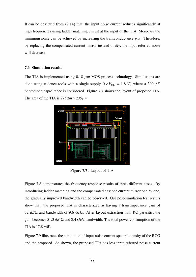
It can be observed from (7.14) that, the input noise current reduces significantly at
high frequencies using ladder matching circuit at the input of the TIA. Moreover the
minimum noise can be achieved by increasing the transconductance gm2. Therefore,
by replacing the compensated current mirror instead of M2, the input referred noise
will decrease.
7.6 Simulation results
The TIA is implemented using 0.18 µm MOS process technology. Simulations are
done using cadence tools with a single supply (i.e.VDD = 1.8 V ) where a 300 f F
photodiode capacitance is considered. Figure 7.7 shows the layout of proposed TIA.
The area of the TIA is 275µm×235µm.
Figure 7.7 : Layout of TIA.
Figure 7.8 demonstrates the frequency response results of three different cases. By
introducing ladder matching and the compensated cascode current mirror one by one,
the gradually improved bandwidth can be observed. Our post-simulation test results
show that, the proposed TIA is characterized as having a transimpedance gain of
52 dBΩ and bandwidth of 9.6 GHz. After layout extraction with RC parasitic, the
gain becomes 51.3 dB.Ω and 8.4 GHz bandwidth. The total power consumption of the
TIA is 17.8 mW .
Figure 7.9 illustrates the simulation of input noise current spectral density of the RCG
and the proposed. As shown, the proposed TIA has less input referred noise current
88

Figure 7.8 : The frequency response results of the TIA.
than the RGC configuration. The simulation result shows an equivalent input noise
current spectral density below 20p A/√
Hz within the bandwidth.
Figure 7.10 shows the group-delay variation with frequency. The TIA has a minimum
group delay of −6ps, increases to 13 ps within the bandwidth of 8.4 GHz.
Figure 7.9 : Spectral density of the input noise current as a function of frequency.
Figure 7.10 : The group delay variation of TIA.
89

To study the impact of the process variations on the frequency response of the TIA,
a set of 100 samples has been chosen for Monte Carlo simulation. As shown in
Figure 7.11, the frequency response has a small variation due to process variation and
mismatching. To make the design more realistic, corner analysis is used to simulate the
circuit in different operational conductions, such as different temperatures and altered
process corners.
Figure 7.11 : Monte Carlo simulation results for frequency response for 100 samples.
Figure 7.12 shows the transient response of the TIA at different process corners for
10 µAp−p input current pulse. The simulation results show that, the proposed TIA can
operate normally at various process corners for wide bandwidth. Table 7.1 shows a
Figure 7.12 : Transient response of the TIA under different corners.
comparison of the performance of proposed TIA with those recently reported in the
literature. The performance figures show that the bandwidth of the proposed TIA for
a high photodiode capacitance is higher than the other TIA circuits while its power
dissipation is the lowest.
90

Table 7.1 : Performance Comparison of Recent CMOS TIAs.
Ref. Cpd Gain BW Power Noise( f F) (dBΩ) (GHz) (mW ) (pA/
√Hz)
This worka 300 51.3 8.4 17.8 20[128]b 200 58.7 2.6 47 13[129]a 300 56.7 5.0 27.3 21[33]b 250 61.0 7.2 70.2 8.2[130]a 200 59.8 2.9 25.4 13.1[36]b 250 53 8.0 135 18[38]b 300 54 7.0 18.6 18
a: Simulation results, b: Measurement results
7.7 Conclusion
The proposed TIA design offers a good technique to improve the input noise and
bandwidth performances of the conventional RCG TIA. The technique is based using
cascode current mirror with resistive compensation technique and a ladder matching
network. The TIA is implemented in TSMC 180 nm CMOS technology with 1.8 V
supply voltage. It is observed that the TIA provides -3 dB bandwidth of 8.4GHz,
transimpedance gain of 51.3 dBΩ in the presence of a 300 f F photodiode capacitance
and input referred noise current spectral density of 20 pA/√
Hz. TIA consumes
17.8 mW . Simulation results show that the TIA displays a broadband flat response and
an ultra-low noise performance with lower power in comparison with other techniques.
Therefore, it is very proficient for applications in optical transceivers.
91

92

8. CONCLUSIONS AND RECOMMENDATIONS
All over this thesis, the most significant results and main conclusions have been
encapsulate in the final section of each chapter. In this final chapter, the most
remarkable contributions will be presented to provide a general synopsis of the whole
work. First, the main objectives presented in the first chapter will be considered,
confirming their achievement and leading to the conformable conclusions. Finally,
further works will be pointed out.
The major need for today’s optical communication devices is to operate at wider
band such as to support high speed Internet, multimedia communication and similarly
many more broadband services. Due to integration and cost advantages of CMOS
technologies, CMOS has encouraged extensive work on developing the optical
communication system.
This thesis has covered in-depth the design of the first building block in the optical
receiver system: the transimpedance amplifier (TIA). The goal of TIA consists of
converting the small photodiode current into a voltage as efficiently as possible. This
research provides the necessary background knowledge to fully understand the analysis
and design of the transimpedance amplifier (TIA). Due to which many studies and
researches are being done throughout the globe, the two most serious limitations of the
TIA design are its transimpedance gain and bandwidth.
Bridging the gap between system and circuit design is done by:
• Understanding the bandwidth expansion by mathematical analysis.
• Introducing new circuit architectures that can be realized.
• Demonstrating implementation of the proposed designs using extensive simulations
in CMOS technology.
93

Tabl
e8.
1:S
umm
ary
ofT
IAba
ndw
idth
enha
ncem
entt
echn
ique
s.
no.
Tech
niqu
eIm
prov
emen
ttec
hniq
ues
Adv
anta
ges
Dra
wba
cks
/Iss
ues
1N
egat
ive
Impe
danc
eIn
crea
seth
ega
in,
de-
crea
seth
ein
put
resi
s-ta
nce
and
mai
ntai
nth
esa
me
time
ofth
eou
tput
pole
.
The
band
wid
thdi
rect
lyde
pend
son
the
gain
Aof
the
ampl
ifier
.It
has
ahi
ghpr
iori
tyin
pres
ence
ofla
rge
phot
odio
deca
paci
tanc
e.T
hesi
zeof
the
chip
usin
gis
smal
ler
than
that
ofth
ech
ips
usin
gpa
ssiv
ede
vice
s.T
heT
IAdo
esno
tde
pend
onQ
-val
uebe
caus
eit
uses
only
activ
ede
vice
san
dre
sist
ors.
Cou
ldno
tbe
appl
ied
atth
ein
put
node
.Itc
onsu
mes
high
pow
er.
2M
atch
ing
netw
orks
Elim
inat
eor
min
imiz
eth
eun
wan
ted
reac
tanc
eth
roug
ha
rang
eof
fre-
quen
cies
.
Lar
geph
otod
iode
para
sitic
capa
cita
nce
can
beis
olat
edan
dit
isgo
odfo
rno
ise
perf
orm
ance
and
low
pow
erco
nsum
p-tio
n.
Itha
sth
etr
ade-
off
betw
een
the
band
wid
than
dco
mpl
exity
.T
hech
ipar
eaoc
cupi
edla
rge
size
.Itbe
com
esm
ore
tric
kyw
hen
real
part
sof
the
term
inat
ions
are
inco
mm
ensu
rate
,or
whe
nth
eyha
veco
mpl
exim
peda
nces
.Ith
asm
ore
nois
eso
urce
s.
3M
odifi
catio
nin
put
stag
eL
ower
impe
danc
ecu
rren
tam
plifi
erin
put
stag
e.
The
band
wid
thca
nbe
optim
ized
be-
caus
eit
isin
depe
nden
tof
the
phot
odi-
ode
capa
cita
nce.
larg
ech
ipar
ea,C
Gha
slo
wtr
an-
sim
peda
nce
gain
,m
ore
nois
eso
urce
s.
4
Usi
nga
casc
ode
curr
ent
mir
ror
with
Res
ista
nce
com
pens
atio
n
Zer
o-po
leca
ncel
latio
nSi
mpl
ede
sign
.,It
boot
sth
eba
ndw
idth
ofcu
rren
tm
irro
rsch
angi
ngth
eD
Cch
arac
teri
stic
sof
the
orig
inal
circ
uits
.
Lar
geg m
isre
quir
edw
hich
cost
lyin
term
sof
pow
erco
nsum
ptio
n.T
heT
IAbe
com
esun
stab
ledu
eto
the
inco
rrec
tzer
o-po
leca
ncel
-la
tion,
Indu
ctor
area
and
CG
has
low
tran
sim
peda
nce
gain
,m
ore
nois
eso
urce
s.
94

In this thesis, in order to fulfill the transimpedance amplifier requirements, various
bandwidth enhancement techniques been proposed to improve the bandwidth of
CMOS TIAs in this study as shown in Table 8.1. Figure 8.1 shows the performances
comparison of TIA bandwidth enhancement techniques.
(a) Bandwidth (b) Power
(c) Noise (d) Area
Figure 8.1 : Performances comparison of TIA bandwidth enhancement techniques.
First, we provided the principle of the negative impedance circuit. We developed a
theory that analytically related to the bandwidth extension. We proposed a new TIA
topology based on employing a negative impedance circuit. We demonstrated the
proposed TIA in 0.18 µm CMOS technology that was successfully simulated up to
7 GHz and provides up to 54.3 dBΩ transimpedance amplifier.
One major advantage of negative impedance technique is its priority in presence
of large photodiode capacitance because the bandwidth directly depends on the
gain A of the amplifier. Furthermore, this technique uses only active devices and
resistors which makes the TIA does not depend on Q-value and parasitic effect of
on-chip components, unlike the inductive-peaking and capacitive-peaking techniques.
Moreover, the size of the chip using this topology is smaller than that of the chips
using passive devices. The major disadvantage of negative impedance technique is its
95

higher power dissipation.
Second, we proposed a wide band transimpedance amplifier using the matching
technique. It is shown that by simultaneously using of series input matching topology
and T-output matching network, the bandwidth of the TIA can be obviously improved.
We demonstrated a CMOS 0.18 µm CMOS TIA that operates up to bandwidth of
20 GHz with a transimpedance gain of 52.6 dBΩ. The matching technique gives us
several advantages. First we can avoid large photodiode parasitic capacitance. Second,
it is good for noise performance. Third it has low power consumption. The drawback
of this approach is the trade-off between the bandwidth and complexity. Another
disadvantage of using passive inductors is that makes the chip area occupied large size.
Third, we introduced a novel architecture to extend the bandwidth of the TIA. This
TIA employs a parallel combination of two series resonate circuits with different
resonate frequencies on the conventional regulated common gate (RGC) architecture.
This methodology is supported by a design example in a 0.18 µm CMOS process .
The proposed TIA is founded to have a 53 dBΩ transimpedance gain over 13 GHz
bandwidth and less noise than RCG topology. The main advantage of this topology
is that photodiode capacitance is decoupled from the TIA input by the common
base stage. Hence the bandwidth can be optimized because it is independent of the
photodiode capacitance. Furthermore, it has an additional significant noise source,
what is the main obstacle of this technique. Also the power consumption will be
higher because more devices are used in the modification input stage.
Finally, we developed a novel TIA architecture that enables to achieve a bandwidth of
8.4 GHz . The technique is based on using a cascode current mirror with resistive
compensation technique and a ladder matching network. The simulation results show
that, the propose TIA achieved a bandwidth of 8.4 GHz, a transimpedance gain of
51.3 dBΩ and input referred noise current spectral density of 20 pA/√
Hz . The
average group-delay variation is 4 ps over the −3dB bandwidth and the TIA consumes
17.8 mW from a 1.8 V supply. The primary benefits of this technique are its simple
design, that can be designed independently of the main TIA to reduce input impedance.
96

Also, the resistive compensation technique boots the bandwidth of current mirrors
without changing the DC characteristics of the original circuits. There are also two
major drawbacks associated with this technique. When the load capacitance is large,
a large gm is required which costly in terms of power consumption. Moreover, the
passive resistance has a large tolerance and it varies with process and temperature
which does not track transconductance of the MOS transistor because. This will add
extra noise source, power consumption and increase the chip area.
8.1 Future works
Overall, this thesis provides insight and proposes useful techniques to improve the
bandwidth of the transimpedance amplifier. It presents exhaustive understanding of
the methodology to enhance the bandwidth bandwidth of the transimpedance amplifier
and highlights on basic concepts which have been usually ignored in the literature. An
accurate and deep understanding of these mechanisms offers many opportunities to
extend this research to new areas and further on transimpedance amplifiers.
• Commonly, the impact of bandwidth enhancement techniques on the other
parameters has been unheeded in the literature. Further research can begin to
consider the effect of the bandwidth extension techniques on other parameters
focusing on phase, group delay, etc with these types of TIAs.
• The next step would be moving on the need for a more comprehensive of the
noise analysis to investigate way to further minimize the noise while improving
the bandwidth. In the proposed topologies, it was shown that once the noise source
and procedure was understood, necessary techniques could be taken to reduce the
source of the noise which is in itself a huge topic.
Moreover the noise generated by a huge number of transistor could affect the
sensitivity of the receiver . This problem can be solved by isolate the core of
the transimpedance amplifier. So that, more research on isolation technique are
mandatory.
Furthermore, the noise analysis can also be done that includes a model for the bond
wire. It has been reported that, the bond wire has a serious impact on the TIA
97

bandwidth and noise performance. It should be possible obtain better performance
by optimizing the TIA performance with the bond wire.
• As previously mentioned the usage of negative impedance circuit at the output
node of the TIA allows to improve the bandwidth of the TIA. Using the negative
impedance circuit can be more generalized in many RF building blocks whose
frequency response or bandwidth is determined by one or two dominant poles .
More research is needed to investigate alternate structures for the design of negative
resistance circuits with high efficiency in the gain and the bandwidth
• Despite the fact that inductors are believed to be area inefficient, inductors do not
presuppose high quality factors. Therefore, a new technique inspired to implement
the inductor in an area-efficient fashion. The active inductors is used to reduce the
chip area of the TIA circuits . However, active inductors have several drawbacks
including: high power consumption and high noise, this work focuses on reducing
the large chip area required to fabricate spiral inductor by using active devices and
reducing the cost. More research is needed to investigate alternate structures of the
active inductor to reduce the power consumption.
98

REFERENCES
[1] Razavi, B. (2012). Design of integrated circuits for optical communications, JohnWiley & Sons.
[2] LaFevre, K., (2011), Design of a Modified Cherry-Hooper TransimpedanceAmplifier with DC Offset Cancellation, (Ph.D. Thesis), Arizona StateUniversity.
[3] Song, I., (2004), Multi-Gbit/s Transimpedance Amplifier with IntegratedPhotodetector for Optional Interconnects, (Ph.D. Thesis), Citeseer.
[4] Razavi, B. (2001). Design of Analog CMOS Integrated Circuits, McGraw-Hill,Inc., New York, NY, USA, 1 edition.
[5] Mohan, S.S., Hershenson, M.D.M., Boyd, S.P. and Lee, T.H. (2000). Bandwidthextension in CMOS with optimized on-chip inductors, Solid-StateCircuits, IEEE Journal of, 35(3), 346–355.
[6] Razavi, B. (2002). Prospects of CMOS technology for high-speed opticalcommunication circuits, Solid-State Circuits, IEEE Journal of, 37(9),1135–1145.
[7] Galal, S. and Razavi, B. (2004). 40-Gb/s amplifier and ESD protection circuitin 0.18um CMOS technology, IEEE J. Solid-State Circuits, 39(12),2389–2396.
[8] Jin, J.D. and Hsu, S.S. (2008). A 40-Gb/s transimpedance amplifier in0.18-m CMOS technology, Solid-State Circuits, IEEE Journal of, 43(6),1449–1457.
[9] Jin, J.D. and Hsu, S.S. (2008). A 75-dB 10-Gb/s Transimpedance Amplifier in0.18-m CMOS Technology, Photonics Technology Letters, IEEE, 20(24),2177–2179.
[10] Ahn, H.T. and Allstot, D.J. (2002). A 0.5-8.5 GHz fully differential CMOSdistributed amplifier, Solid-State Circuits, IEEE Journal of, 37(8),985–993.
[11] Gupta, M., Singh, U. and Srivastava, R. (2014). Bandwidth extension of highcompliance current mirror by using compensation methods, Active andPassive Electronic Components, 2014.
[12] Agrawal, G.P. (2012). Fiber-optic communication systems, volume222, JohnWiley & Sons.
99

[13] Gao, J. (2011). Optoelectronic integrated circuit design and device modeling, JohnWiley & Sons.
[14] Talarico, C., Agrawal, G., Wang-Roveda, J. and Lashgari, H. (2015). DesignOptimization of a Transimpedance Amplifier for a Fiber Optic Receiver,Circuits, Systems, and Signal Processing, 1–16.
[15] Li, C. and Palermo, S. (2013). A low-power 26-GHz transformer-based regulatedcascode SiGe BiCMOS transimpedance amplifier, Solid-State Circuits,IEEE Journal of, 48(5), 1264–1275.
[16] Palais, J.C. (1988). Fiber optic communications, Prentice Hall Englewood Cliffs.
[17] Dutta, N.K. and Wang, Q. (2013). Semiconductor optical amplifiers, Worldscientific.
[18] Hossain, M. and Carusone, A.C. (2010). Multi-Gb/s bit-by-bit receiverarchitectures for 1-D partial-response channels, Circuits and Systems I:Regular Papers, IEEE Transactions on, 57(1), 270–279.
[19] Donati, S. (2001). Photodetectors: devices, circuits, and applications, Measure-ment Science and Technology, 12(5), 653.
[20] Yang, J.T., Lee, Y.H., Wu, M.J., Huang, Y.Y., Mu, Y.M., Lin, Q., Chen,S. and Xu, A. (2008). A CMOS multi-band low noise amplifier usinghigh-Q active inductors, WSEAS International Conference. Proceedings.Mathematics and Computers in Science and Engineering, 8, WorldScientific and Engineering Academy and Society.
[21] Yuan, F. (2007). CMOS current-mode circuits for data communications, SpringerScience & Business Media.
[22] Wu, M., Lee, Y., Huang, Y., Mu, Y. and Yang, J. (2007). A CMOS multi-bandlow noise amplifier using high-Q active inductors, Int. J. Circuits Syst.Signal Process, 2(2), 199–202.
[23] Analui, B. and Hajimiri, A. (2002). Multi-pole bandwidth enhancementtechnique for trans-impedance amplifiers, Solid-State Circuits Conference,2002. ESSCIRC 2002. Proceedings of the 28th European, IEEE,pp.303–306.
[24] Chien, F.T. and Chan, Y.J. (1999). Bandwidth enhancement of transimpedanceamplifier by a capacitive-peaking design, Solid-State Circuits, IEEEJournal of, 34(8), 1167–1170.
[25] Kuo, C.W., Hsiao, C.C., Yang, S.C. and Chan, Y.J. (2001). 2 Gbit/stransimpedance amplifier fabricated by 0.35 µm CMOS technologies,Electronics letters, 37(19), 1158–1160.
[26] Tanabe, A., Soda, M., Nakahara, Y., Tamura, T., Yoshida, K. and Furukawa,A. (1998). A single-chip 2.4-Gb/s CMOS optical receiver IC with lowsubstrate cross-talk preamplifier, Solid-State Circuits, IEEE Journal of,33(12), 2148–2153.
100
[27] Yoon, T. and Jalali, B. (1998). Front-end CMOS chipset for fiber-basedgigabit Ethernet, VLSI Circuits, 1998. Digest of Technical Papers. 1998Symposium on, IEEE, pp.188–191.
[28] Säckinger, E. and Fischer, W.C. (2000). A 3-GHz 32-dB CMOS limitingamplifier for SONET OC-48 receivers, Solid-State Circuits, IEEE Journalof, 35(12), 1884–1888.
[29] Kim, S.E., Song, S.J., Park, S.M. and Yoo, H.J. (2003). CMOS opticalreceiver chipset for gigabit Ethernet applications, Circuits and Systems,2003. ISCAS’03. Proceedings of the 2003 International Symposium on,volume 1, IEEE, pp.I–29.
[30] Mohan, S.S., del Mar Hershenson, M., Boyd, S.P. and Lee, T.H. (1999). Simpleaccurate expressions for planar spiral inductances, Solid-State Circuits,IEEE Journal of, 34(10), 1419–1424.
[31] Kromer, C., Sialm, G., Morf, T., Schmatz, M.L., Ellinger, F., Erni, D.and Jäckel, H. (2004). A low-power 20-GHz 52-dBΩ transimpedanceamplifier in 80-nm CMOS, Solid-State Circuits, IEEE Journal of, 39(6),885–894.
[32] Hasan, S.R. (2005). Design of a low-power 3.5-GHz broad-band CMOStransimpedance amplifier for optical transceivers, Circuits and Systems I:Regular Papers, IEEE Transactions on, 52(6), 1061–1072.
[33] Wu, C.H., Lee, C.H., Chen, W.S. and Liu, S.I. (2005). CMOS widebandamplifiers using multiple inductive-series peaking technique, Solid-StateCircuits, IEEE Journal of, 40(2), 548–552.
[34] Chalvatzis, T., Yau, K.H., Aroca, R., Schvan, P., Yang, M.T., Voinigescu, S.P.et al. (2007). Low-voltage topologies for 40-Gb/s circuits in nanoscaleCMOS, Solid-State Circuits, IEEE Journal of, 42(7), 1564–1573.
[35] Chan, C.T. and Chen, O.T. (2006). Inductor-less 10Gb/s CMOS transimpedanceamplifier using source-follower regulated cascode and double three-orderactive feedback, Circuits and Systems, 2006. ISCAS 2006. Proceedings.2006 IEEE International Symposium on, IEEE, pp.4–pp.
[36] Lu, Z., Yeo, K.S., Ma, J., Do, M.A., Lim, W.M. and Chen, X. (2007).Broad-band design techniques for transimpedance amplifiers, Circuits andSystems I: Regular Papers, IEEE Transactions on, 54(3), 590–600.
[37] Ngo, T.H., Lee, T.W. and Park, H.H. (2010). Design of transimpedance amplifierfor optical receivers in 0.13 µm CMOS, Optical Internet (COIN), 20109th International Conference on, IEEE, pp.1–3.
[38] Lu, Z., Yeo, K.S., Lim, W.M., Do, M.A. and Boon, C.C. (2010). Design of aCMOS broadband transimpedance amplifier with active feedback, VeryLarge Scale Integration (VLSI) Systems, IEEE Transactions on, 18(3),461–472.
101

[39] Bashiri, S., Plett, C., Aguirre, J. and Schvan, P. (2010). A 40 Gb/stransimpedance amplifier in 65 nm CMOS, Circuits and Systems(ISCAS), Proceedings of 2010 IEEE International Symposium on, IEEE,pp.757–760.
[40] Chan, C.Y., Chen, S.C., Tsai, M.H. and Hsu, S.S. (2008). Wiring effectoptimization in 65-nm low-power NMOS, Electron Device Letters, IEEE,29(11), 1245–1248.
[41] Kim, J. and Buckwalter, J.F. (2012). A 40-Gb/s optical transceiver front-end in45 nm SOI CMOS, Solid-State Circuits, IEEE Journal of, 47(3), 615–626.
[42] Chou, S.T., Huang, S.H., Hong, Z.H. and Chen, W.Z. (2012). A 40 Gbps opticalreceiver analog front-end in 65 nm CMOS, Circuits and Systems (ISCAS),2012 IEEE International Symposium on, IEEE, pp.1736–1739.
[43] Burlando, P. (1993). Forecasting of short-term rainfall using ARMA models,Journal of Hydrology, 144, 193–211.
[44] Davari, B. (1999). CMOS technology: Present and future, VLSI Circuits, 1999.Digest of Technical Papers. 1999 Symposium on, IEEE, pp.5–10.
[45] Tavernier, F. and Steyaert, M. (2011). High-speed optical receivers withintegrated photodiode in nanoscale CMOS, volume 5, Springer Science& Business Media.
[46] Tavernier, F. and Steyaert, M.S. (2009). High-speed optical receivers withintegrated photodiode in 130 nm CMOS, Solid-State Circuits, IEEEJournal of, 44(10), 2856–2867.
[47] Hossain, M. and Carusone, A.C. (2010). Multi-Gb/s bit-by-bit receiverarchitectures for 1-D partial-response channels, Circuits and Systems I:Regular Papers, IEEE Transactions on, 57(1), 270–279.
[48] Razavi, B. (2012). Design of integrated circuits for optical communications, JohnWiley & Sons.
[49] Sansen, W.M. (2007). Analog design essentials, volume859, Springer Science &Business Media.
[50] Hullett, J. and Muoi, T. (1976). A feedback receive amplifier for opticaltransmission systems, IEEE Transactions on Communications, 24,1180–1185.
[51] Williams, G.F. and LeBlanc, H.P. (1986). Active feedback lightwave receivers,Lightwave Technology, Journal of, 4(10), 1502–1508.
[52] Horowitz, M. (2008). Scaling, power, and the future of CMOS technology, DeviceResearch Conference, 2008, IEEE, pp.7–8.
[53] Cherry, E.M. and Hooper, D. (1963). The design of wide-band transistorfeedback amplifiers, Proceedings of the Institution of Electrical Engineers,volume110, IET, pp.375–389.
102
[54] Holdenried, C.D., Haslett, J.W. and Lynch, M.W. (2004). Analysis and designof HBT Cherry-Hooper amplifiers with emitter-follower feedback foroptical communications, Solid-State Circuits, IEEE Journal of, 39(11),1959–1967.
[55] Chan, Y.J., Chien, F.T., Shin, T.T. and Ho, W.J., (2002), Bandwidthenhancement of transimpedance amplifier by capacitive peaking design,uS Patent 6,353,366.
[56] Kuo, C.W., Hsiao, C.C., Yang, S.C. and Chan, Y.J. (2001). 2 Gbit/stransimpedance amplifier fabricated by 0.35 µm CMOS technologies,Electronics letters, 37(19), 1158–1160.
[57] Analui, B. and Hajimiri, A. (2004). Bandwidth enhancement for transimpedanceamplifiers, Solid-State Circuits, IEEE Journal of, 39(8), 1263–1270.
[58] Galal, S. and Razavi, B. (2003). 10-Gb/s limiting amplifier and laser/modulatordriver in 0.18-µm CMOS technology, Solid-State Circuits, IEEE Journalof, 38(12), 2138–2146.
[59] Nahin, P.J. (1983). Among the giants: Oliver Heaviside: Genius andcurmudgeon: He called establishment mathematicianswoodenheaded,when his powerful new methods perplexed them. His fellow EEs didn’tknow what to make of him either, Spectrum, IEEE, 20(7), 63–69.
[60] Analui, B. and Hajimiri, A. (2004). Bandwidth enhancement for transimpedanceamplifiers, Solid-State Circuits, IEEE Journal of, 39(8), 1263–1270.
[61] Staric, P. and Margan, E. (2007). Wideband amplifiers, Springer Science &Business Media.
[62] Scott, D.E. (1987). An introduction to circuit analysis, McGraw-Hill New Yorketc.
[63] Suárez, A. (2009). Analysis and design of autonomous microwave circuits,volume190, John Wiley & Sons.
[64] Peterson, A., Kiziloglu, K., Yoon, T., Williams Jr, F. and Sander, M. (2003).Front-end CMOS chipset for 10 Gb/s communication, IEEE RFIC Symp,Dig., Seattle, 93A96.
[65] Yuan, F. (2007). CMOS current-mode circuits for data communications, SpringerScience & Business Media.
[66] Ballweber, B.M., Gupta, R. and Allstot, D.J. (2000). A fully integrated 0.5-5.5GHz CMOS distributed amplifier, Solid-State Circuits, IEEE Journal of,35(2), 231–239.
[67] Park, S.M. and Yoo, H.J. (2004). 1.25-Gb/s regulated cascode CMOStransimpedance amplifier for gigabit ethernet applications, Solid-StateCircuits, IEEE Journal of, 39(1), 112–121.
103
[68] Lee, H. and Mok, P.K. (2003). Active-feedback frequency-compensationtechnique for low-power multistage amplifiers, Solid-State Circuits, IEEEJournal of, 38(3), 511–520.
[69] Han, J., Choi, B., Seo, M., Yun, J., Lee, D., Kim, T., Eo, Y. and Park, S.M.(2010). A 20-Gb/s transformer-based current-mode optical receiver in0.13-CMOS, Circuits and Systems II: Express Briefs, IEEE Transactionson, 57(5), 348–352.
[70] Taghavi, M., Belostotski, L. and Haslett, J. (2012). A bandwidth enhancementtechnique for CMOS TIAs driven by large photodiodes, New Circuits andSystems Conference (NEWCAS), 2012 IEEE 10th International, IEEE,pp.433–436.
[71] Momeni, O., Hashemi, H. and Afshari, E. (2010). A 10-Gb/s inductorlesstransimpedance amplifier, Circuits and Systems II: Express Briefs, IEEETransactions on, 57(12), 926–930.
[72] Park, S.M. and Toumazou, C. (2000). A packaged low-noise high-speedregulated cascode transimpedance amplifier using a 0.6 µm N-wellCMOS technology, Solid-State Circuits Conference, 2000. ESSCIRC’00.Proceedings of the 26rd European, IEEE, pp.431–434.
[73] Lee, J., Song, S.J., Park, S.M., Nam, C.M., Kwon, Y.S. and Yoo, H.J.(2002). A multichip on oxide of 1 Gb/s 80 dB fully-differential CMOStransimpedance amplifier for optical interconnect applications, Solid-StateCircuits Conference, 2002. Digest of Technical Papers. ISSCC. 2002 IEEEInternational, volume 1, IEEE, pp.80–447.
[74] Zand, B., Phang, K., Johns, D.A. et al. (2001). A transimpedance amplifierwith DC-coupled differential photodiode current sensing for wirelessoptical communications, PROCEEDINGS OF THE IEEE CUSTOMINTEGRATED CIRCUITS CONFERENCE, IEEE; 1999, pp.455–458.
[75] Thanachayanont, A. and Payne, A. (1996). VHF CMOS integrated activeinductor, Electronics Letters, 32(11), 999–1000.
[76] Wu, Y., Ding, X., Ismail, M. and Olsson, H. (2003). RF bandpass filter designbased on CMOS active inductors, Circuits and Systems II: Analog andDigital Signal Processing, IEEE Transactions on, 50(12), 942–949.
[77] Gao, Z., Yu, M., Ye, Y. and Ma, J. (2005). Wide tuning range of a CMOS RFbandpass filter for wireless applications, Electron Devices and Solid-StateCircuits, 2005 IEEE Conference on, IEEE, pp.53–56.
[78] Sae-Ngow, S. and Thanachayanont, A. (2003). A low-voltage, wide dynamicrange CMOS floating active inductor, TENCON 2003. Conference onConvergent Technologies for the Asia-Pacific Region, volume 4, IEEE,pp.1460–1463.
[79] Thanachayanont, A. (2002). CMOS transistor-only active inductor for IF/RFapplications, Industrial Technology, 2002. IEEE ICIT’02. 2002 IEEEInternational Conference on, volume 2, IEEE, pp.1209–1212.
104
[80] Akbari-Dilmaghani, R., Payne, A. and Toumazou, C. (1998). A high Q RFCMOS differential active inductor, Electronics, Circuits and Systems,1998 IEEE International Conference on, volume 3, IEEE, pp.157–160.
[81] Thanachayanont, A. and Payne, A. (2000). CMOS floating active inductorand its applications to bandpass filter and oscillator designs, IEEProceedings-Circuits, Devices and Systems, 147(1), 42–48.
[82] Grozing, M., Pascht, A. and Berroth, M. (2001). A 2.5 V CMOS differentialactive inductor with tunable L and Q for frequencies up to 5GHz, Microwave Symposium Digest, 2001 IEEE MTT-S International,volume 1, IEEE, pp.575–578.
[83] Beiju, H., Xu, Z. and Hongda, C. (2009). 1-Gb/zero-pole cancellation CMOStransimpedance amplifier for Gigabit Ethernet applications, Journal ofSemiconductors, 30(10), 105005.
[84] Chong, Z.Y. and Sansen, W. (2013). Low-noise wide-band amplifiers in bipolarand CMOS technologies, volume117, Springer Science & Business Media.
[85] Abu-Taha, J. and Yazgi, M. (2015). A 6.03 GHz Low Power TransimpedanceAmplifier TIA in CMOS 0.18µm Technology, IJETAE InternationalJournal of Emerging Technology and Advanced Engineering, 5(2), 37–46.
[86] Aitchison, C.S. (1985). The intrinsic noise figure of the MESFET distributedamplifier, Microwave Theory and Techniques, IEEE Transactions on,33(6), 460–466.
[87] Liu, L., Zou, J., Ma, N., Zhu, Z. and Yang, Y. (2015). A CMOS transimpedanceamplifier with high gain and wide dynamic range for optical fiber sensingsystem, Optik-International Journal for Light and Electron Optics,126(15), 1389–1393.
[88] Raut, R. and Ghasemi, O. (2008). A power efficient wide band trans-impedanceamplifier in sub-micron CMOS integrated circuit technology, Circuits andSystems and TAISA Conference, 2008. NEWCAS-TAISA 2008. 2008 Joint6th International IEEE Northeast Workshop on, IEEE, pp.113–116.
[89] Sangirov, J., Ukaegbu, I.A., Nguyen, N.T., Lee, T.W., Cho, M.H. and Park,H.H. (2014). Design of small-area transimpedance optical receiver modulefor optical interconnects, Advanced Communication Technology (ICACT),2014 16th International Conference on, IEEE, pp.283–289.
[90] Ngo, T.H., Lee, T.W. and Park, H.H. (2011). 4.1 mW 50 dBΩ 10 Gbpstransimpedance amplifier for optical receivers in 0.13 µm CMOS,Microwave and Optical Technology Letters, 53(2), 448–451.
[91] Zhenghao, L., Dandan, C. and Seng, Y.K. (2009). An inductor-less broadbanddesign technique for transimpedance amplifiers, Integrated Circuits,ISIC’09. Proceedings of the 2009 12th International Symposium on, IEEE,pp.232–235.
105

[92] Seng, C.W., Sern, T.Y. and Seng, Y.K. (2013). A low power widebanddifferential transimpedance amplifier for optical receivers in 0.18-µmCMOS, New Circuits and Systems Conference (NEWCAS), 2013 IEEE11th International, IEEE, pp.1–4.
[93] Oh, Y.H. and Lee, S.G. (2004). An inductance enhancement technique and itsapplication to a shunt-peaked 2.5 Gb/s transimpedance amplifier design,Circuits and Systems II: Express Briefs, IEEE Transactions on, 51(11),624–628.
[94] Yu, Y., Baltus, P.G. and Van Roermund, A.H. (2011). Integrated 60 GHz RFbeamforming in CMOS, Springer Science & Business Media.
[95] Fan, X., Zhang, H. and Sánchez-Sinencio, E. (2008). A noise reductionand linearity improvement technique for a differential cascode LNA,Solid-State Circuits, IEEE Journal of, 43(3), 588–599.
[96] Abidi, A.A. (2004). RF-CMOS comes of age, IEICE transactions on electronics,87(6), 840–853.
[97] Marzuki, A. (2011). Advances in Monolithic Microwave Integrated Circuits forWireless Systems: Modeling and Design Technologies: Modeling andDesign Technologies, IGI Global.
[98] Chen, W.H., Liu, G., Zdravko, B. and Niknejad, A.M. (2008). A highly linearbroadband CMOS LNA employing noise and distortion cancellation,Solid-State Circuits, IEEE Journal of, 43(5), 1164–1176.
[99] Chen, K.H., Lu, J.H., Chen, B.J. and Liu, S.I. (2007). An ultra-wide-band0.4–10-GHz LNA in 0.18-µm CMOS, Circuits and Systems II: ExpressBriefs, IEEE Transactions on, 54(3), 217–221.
[100] Govind, V., Dalmia, S. and Swaminathan, M. (2004). Design of integrated lownoise amplifiers (LNA) using embedded passives in organic substrates,Advanced Packaging, IEEE Transactions on, 27(1), 79–89.
[101] Samavati, H., Rategh, H.R. and Lee, T.H. (2000). A 5-GHz CMOS wirelessLAN receiver front end, Solid-State Circuits, IEEE Journal of, 35(5),765–772.
[102] Wadatsumi, J., Kousai, S., Miyashita, D. and Hamada, M. (2008). A 1.2V, 0.1-6.0 GHz, two-stage differential LNA using gain compensationscheme, Silicon Monolithic Integrated Circuits in RF Systems, 2008. SiRF2008. IEEE Topical Meeting on, IEEE, pp.175–178.
[103] Perumana, B.G., Zhan, J.H.C., Taylor, S.S., Carlton, B.R. and Laskar,J. (2008). A 9.2 mW, 4-8 GHz resistive feedback CMOS LNA with24.4 dB gain, 2 dB noise figure, and 21.5 dBm output IP3, SiliconMonolithic Integrated Circuits in RF Systems, 2008. SiRF 2008. IEEETopical Meeting on, IEEE, pp.34–37.
106

[104] Ragheb, T., Nieuwoudt, A. and Massoud, Y. (2006). Modeling of 3.1-10.6ghz cmos filter-based low noise amplifier for ultra-wideband receivers,Wireless and Microwave Technology Conference, 2006. WAMICON’06.IEEE Annual, IEEE, pp.1–5.
[105] Egels, M., Gaubert, J. and Pannier, P. (2006). High frequency LNA designin standard CMOS process, Circuits and Systems, 2006 IEEE North-EastWorkshop on, IEEE, pp.5–8.
[106] Adabi, E., Heydari, B., Bohsali, M. and Niknejad, A.M. (2007). 30 GHzCMOS low noise amplifier, Radio Frequency Integrated Circuits (RFIC)Symposium, 2007 IEEE, IEEE, pp.625–628.
[107] Kiyota, Y., Chen, C.H., Kubodera, T., Nakamura, A., Takeshita, K. and Deen,M. (2007). A new approach of high frequency noise modeling for 70-nmNMOS transistors by accurate noise source extraction, Radio FrequencyIntegrated Circuits (RFIC) Symposium, 2007 IEEE, IEEE, pp.635–638.
[108] Abu-Taha J., Y.M. (2016). A 7 GHz compact transimpedance amplifier TIAin CMOS 0.18µm technology, ANALOG INTEGRATED CIRCUITS ANDSIGNAL PROCESSING, 86(3), pp.429–438.
[109] Gupta, M., Singh, U. and Srivastava, R. (2014). Bandwidth extension of highcompliance current mirror by using compensation methods, Active andPassive Electronic Components, 2014.
[110] Ravikumar, S., (2015), Circuit architectures for high speed CMOS clockand data recovery circuits, (Ph.D. Thesis), University of Illinois atUrbana-Champaign.
[111] Li, C. and Palermo, S. (2013). A low-power 26-GHz transformer-basedregulated cascode SiGe BiCMOS transimpedance amplifier, Solid-StateCircuits, IEEE Journal of, 48(5), 1264–1275.
[112] Hsu, S.S., Cho, W.H., Chen, S.W. and Jin, J.D. (2011). CMOS broad-band amplifiers for optical communications and optical interconnects,Radio-Frequency Integration Technology (RFIT), 2011 IEEE Interna-tional Symposium on, IEEE, pp.105–108.
[113] Mekky, R.H., Cicek, P.V. and El-Gamal, M.N. (2013). Ultra low-powerlow-noise transimpedance amplifier for MEMS-based reference oscil-lators, Electronics, Circuits, and Systems (ICECS), 2013 IEEE 20thInternational Conference on, IEEE, pp.345–348.
[114] Qiwei, S., Luhong, M., Sheng, X. and Yuzhuo, K. (2015). Novelpre-equalization transimpedance amplifier for 10 Gb/s optical intercon-nects, Journal of Semiconductors, 36(7), 075002.
[115] Kim, J. and Buckwalter, J.F. (2010). Bandwidth enhancement with lowgroup-delay variation for a 40-Gb/s transimpedance amplifier, Circuitsand Systems I: Regular Papers, IEEE Transactions on, 57(8), 1964–1972.
107

[116] Al-Juaid, M.S., (1998), Design of variable gain transimpedance preamplifier,(Ph.D. Thesis), King Fahd University of Petroleum and Minerals.
[117] Sedra, S. (2014). Microelectronic Circuits, Oxford University Press.
[118] Levinzon, F., (2015). Comparison of 1/f Noise and Thermal Noise in JFETsand MOSFETs, Piezoelectric Accelerometers with Integral Electronics,Springer, pp.93–106.
[119] Wang, C.Y., Wang, C.S. and Wang, C.K. (2007). An 18-mW two-stage CMOStransimpedance amplifier for 10 Gb/s optical application, Solid-StateCircuits Conference, 2007. ASSCC’07. IEEE Asian, IEEE, pp.412–415.
[120] Säckinger, E. (2010). The transimpedance limit, Circuits and Systems I: RegularPapers, IEEE Transactions on, 57(8), 1848–1856.
[121] Chen, D., Yeo, K.S., Shi, X., Do, M.A., Boon, C.C. and Lim, W.M. (2013).Cross-coupled current conveyor based CMOS transimpedance amplifierfor broadband data transmission, Very Large Scale Integration (VLSI)Systems, IEEE Transactions on, 21(8), 1516–1525.
[122] Greaves, S.D. and Unwin, R.T. (1996). The design of tuned front-end GaAsMMIC optical receivers, Microwave Theory and Techniques, IEEETransactions on, 44(4), 591–597.
[123] Gupta, M., Malhotra, A. and Malik, A. (2012). Low-voltage current mirror withextended bandwidth, Power Electronics (IICPE), 2012 IEEE 5th IndiaInternational Conference on, IEEE, pp.1–5.
[124] Oliveira, L.B., Leitão, C.M. and Silva, M.M. (2012). Noise performanceof a regulated cascode transimpedance amplifier for radiation detectors,Circuits and Systems I: Regular Papers, IEEE Transactions on, 59(9),1841–1848.
[125] de Medeiros Silva, M. and Oliveira, L.B. (2014). Regulated Common-GateTransimpedance Amplifier Designed to Operate With a SiliconPhoto-Multiplier at the Input, Circuits and Systems I: Regular Papers,IEEE Transactions on, 61(3), 725–735.
[126] Kim, J. and Buckwalter, J.F. (2010). A 40-Gb/optical transceiver front-endin 45nm SOI CMOS technology, Custom Integrated Circuits Conference(CICC), 2010 IEEE, IEEE, pp.1–4.
[127] Seifouri, M., Amiri, P. and Rakide, M. (2015). Design of broadbandtransimpedance amplifier for optical communication systems, Microelec-tronics Journal, 46(8), 679–684.
[128] Beaudoin, F. and El-Gamal, M. (2002). A 5-Gbit/CMOS optical receiverfrontend, Circuits and Systems, 2002. MWSCAS-2002. The 2002 45thMidwest Symposium on, volume 3, IEEE, pp.III–168.
[129] Kim, Y.H., Jung, E.S. and Lee, S.S. (2014). Bandwidth enhancement techniquefor CMOS RGC transimpedance amplifier, Electronics Letters, 50(12),882–884.
108

[130] Talarico, C., Agrawal, G. and Wang Roveda, J. (2014). A 60dBO 2.9 GHz 0.18µm CMOS transimpedance amplifier for a fiber optic receiver application,Circuits and Systems (MWSCAS), 2014 IEEE 57th International MidwestSymposium on, IEEE, pp.181–184.
109

110

CURRICULUM VITAE
Name Surname: Jawdat ABU TAHAPlace and Date of Birth: Rafah-Gaza Strip , 1968
Address: Islamic University of Gaza
E-Mail: [email protected]; [email protected]
B.Sc.: University of Science and Technology of Oran - ALGERIA
M.Sc.: ISUFI- University of Lecce ITALY
List of Publications and Patents:
PUBLICATIONS/PRESENTATIONS ON THE THESIS
ABU TAHA J., Yazgi M., A 6.03 GHz Low Power Transimpedance Amplifier TIAin CMOS 0.18µm Technology., International Journal of Emerging Technology andAdvanced Engineering (IJETAE),February 37-46, 2015.
ABU TAHA J., Yazgi M., Broadband Transimpedance Amplifier TIA in CMOS0.18µm Technology Using Matching Technique., ELECO 2015, Proceeding of the2015 9th International Conference on Electrical and Electronics Engineering, ELECO2015, February 26-28, Bursa, Turkey.
ABU TAHA J., Yazgi M., A 7 GHz compact transimpedance amplifier TIA inCMOS 0.18µm technology., Analog Integrated Circuits and Signal Processing, 2016,86(3), pp.429–438.
111

112