
ISSN 1755-4535 Buck half-bridge input-series two … 1755-4535 Buck/half-bridge input-series...
12
Published in IET Power Electronics Received on 21st January 2009 Revised on 8th October 2009 doi: 10.1049/iet-pel.2009.0189 ISSN 1755-4535 Buck/half-bridge input-series two-stage converter T. Qian 1 B. Lehman 2 1 Texas Instruments, Warwick, RI, USA 2 Department of Electrical and Computer Engineering, Northeastern University, Boston, MA 02115, USA E-mail: [email protected] Abstract: This study presents a concept of connecting two-stage DC –DC converters in an input-series connection. An application example is discussed in detail where the first stage utilises two series connected buck converters that have reduced voltage stress. A single second stage is a half-bridge converter and is able to regulate the charge balance of the first stage. The benefits of the topology include: reduced primary switch voltage stress, simple self-driven synchronous rectification for wide input voltage range, self-voltage balancing on intermediate bus capacitors and simple housekeeping power supply. Further, the topology exhibits an unusual ripple match concept that can be utilised to suppress the current ripple of the second stage. Based on the detailed analysis, prototypes with 500–700 V input and 5 V/30 A output are built. Experimental results verify the principle and performance of the new topology. 1 Introduction Although a formal framework for connecting the inputs in DC–DC converters in series was presented in the early 1990s [1, 2], it is only recently that widespread applications are being seen of these topologies [3–12]. When using an input-series connection, a high-voltage input can be shared among different power supplies, thereby reducing voltage stress on the input switches. For example, in [3] input-series connection for an electric train with a 700 V DC bus is used to reduce the switch stress on series connected full-bridge converters, thereby allowing the replacement of the IGBTs with MOSFETs. This had the benefit of permitting higher switching frequency to reduce magnetic size, as well as improve power efficiency. Similar benefits are noted in series (‘stacked’) connections in electric trains in [9]. Other high- voltage bus applications that benefit from input-series and output-parallel connections include converters utilised in hybrid-electric vehicles (300–600 V DC bus) [10, 11],a second step-down DC–DC converter (for traditional AC/ DC converter) that is connected with single-phase power factor correction (PFC) (400 V DC bus) or three-phase PFC (800 V DC bus). Of course, conventional topologies, such as zero voltage switching (ZVS) phase-shifted full bridge [13, 14] are favourable when the voltage stress is not too high, because of their high efficiency and lower part count. However, it is often desirable to have voltage stresses of the main switches to be less than or equal to half of the input voltage, which cannot be achieved by such topologies. Further, there has been intriguing discovery that the input-series connections [12] lead to reduction of total MOSFET switch losses, particularly in Class E converters. This is primarily because of the fact that the R on C oss figure of merit is proportional to non-linear term (V BR ) 4/3 , where V BR is the substantially reduced blocking voltage of the individual MOSFET. The benefit of the series input is that as breakdown voltage decreases, C oss gets bigger for a given die area, but Ron gets smaller faster than C oss gets bigger. In fact, this has led to the utilisation of input-series connections in very high frequency (VHF) converters at the 30 – 300 MHz band. The purpose of this paper is to explore a new topology of input series and self-balanced DC – DC converters. Our original motivation was for the development of a V in ¼ 600 V, V out ¼ 28 V, 100 W driver for IGBT inside an electric vehicle, such as those being investigated by the US Army [10, 11]. Our approach is to combine the ideas of input-series output-parallel converters with two-stage converters [15–20]. At the same time, we borrow concepts from multi-level DC –DC converters and inverters to solve IET Power Electron., 2010, Vol. 3, Iss. 6, pp. 965–976 965 doi: 10.1049/iet-pel.2009.0189 & The Institution of Engineering and Technology 2010 www.ietdl.org
Transcript of ISSN 1755-4535 Buck half-bridge input-series two … 1755-4535 Buck/half-bridge input-series...

IEdo
www.ietdl.org
Published in IET Power ElectronicsReceived on 21st January 2009Revised on 8th October 2009doi: 10.1049/iet-pel.2009.0189
ISSN 1755-4535
Buck/half-bridge input-seriestwo-stage converterT. Qian1 B. Lehman2
1Texas Instruments, Warwick, RI, USA2Department of Electrical and Computer Engineering, Northeastern University, Boston, MA 02115, USAE-mail: [email protected]
Abstract: This study presents a concept of connecting two-stage DC–DC converters in an input-series connection.An application example is discussed in detail where the first stage utilises two series connected buck convertersthat have reduced voltage stress. A single second stage is a half-bridge converter and is able to regulate thecharge balance of the first stage. The benefits of the topology include: reduced primary switch voltage stress,simple self-driven synchronous rectification for wide input voltage range, self-voltage balancing onintermediate bus capacitors and simple housekeeping power supply. Further, the topology exhibits an unusualripple match concept that can be utilised to suppress the current ripple of the second stage. Based on thedetailed analysis, prototypes with 500 –700 V input and 5 V/30 A output are built. Experimental results verifythe principle and performance of the new topology.
Ti
1 IntroductionAlthough a formal framework for connecting the inputs inDC–DC converters in series was presented in the early1990s [1, 2], it is only recently that widespread applicationsare being seen of these topologies [3–12]. When using aninput-series connection, a high-voltage input can be sharedamong different power supplies, thereby reducing voltagestress on the input switches. For example, in [3] input-seriesconnection for an electric train with a 700 V DC bus is usedto reduce the switch stress on series connected full-bridgeconverters, thereby allowing the replacement of the IGBTswith MOSFETs. This had the benefit of permitting higherswitching frequency to reduce magnetic size, as well asimprove power efficiency. Similar benefits are noted in series(‘stacked’) connections in electric trains in [9]. Other high-voltage bus applications that benefit from input-series andoutput-parallel connections include converters utilised inhybrid-electric vehicles (�300–600 V DC bus) [10, 11], asecond step-down DC–DC converter (for traditional AC/
DC converter) that is connected with single-phase powerfactor correction (PFC) (�400 V DC bus) or three-phasePFC (�800 V DC bus).
Of course, conventional topologies, such as zero voltageswitching (ZVS) phase-shifted full bridge [13, 14] are
Power Electron., 2010, Vol. 3, Iss. 6, pp. 965–976: 10.1049/iet-pel.2009.0189
favourable when the voltage stress is not too high, becauseof their high efficiency and lower part count. However, it isoften desirable to have voltage stresses of the main switchesto be less than or equal to half of the input voltage, whichcannot be achieved by such topologies. Further, there hasbeen intriguing discovery that the input-series connections[12] lead to reduction of total MOSFET switch losses,particularly in Class E converters. This is primarily becauseof the fact that the RonCoss figure of merit is proportionalto non-linear term (VBR)4/3, where VBR is the substantiallyreduced blocking voltage of the individual MOSFET. Thebenefit of the series input is that as breakdown voltagedecreases, Coss gets bigger for a given die area, but Rongets smaller faster than Coss gets bigger. In fact, this has ledto the utilisation of input-series connections in very highfrequency (VHF) converters at the 30–300 MHz band.
The purpose of this paper is to explore a new topology ofinput series and self-balanced DC–DC converters. Ouroriginal motivation was for the development of aVin ¼ 600 V, Vout ¼ 28 V, 100 W driver for IGBT insidean electric vehicle, such as those being investigated by theUS Army [10, 11]. Our approach is to combine the ideasof input-series output-parallel converters with two-stageconverters [15–20]. At the same time, we borrow conceptsfrom multi-level DC–DC converters and inverters to solve
965
& The Institution of Engineering and Technology 2010
966
&
www.ietdl.org
the capacitor self-balancing voltage problem for input-seriesconnections. That is, whenever the inputs of two convertersare connected in series, their input capacitors may havevoltage imbalances that may lead to transformer saturation,increased losses because of ringing and difficult controlregulation [3, 12, 21–24]. To achieve voltage balancing,both active and passive balancing circuits are often added,unless the specific topology has self-balancing properties[22], which we claim for our proposed topology. Someother interesting performance features of the topology include:
† Lower switch stress: When two buck circuits are connectedin series for the first stage, the voltage stress is reduced to halfof the input voltage. The voltage stress of the switches in thesecond stage is also lower than half of the input voltage whenthe duty ratio of each buck is below 50%. Thus, the approachmaintains the advantages of traditional input-series (or‘stacked’) output-parallel converters [1–12].
† Output-inductorless half-bridge can be utilised for the secondstage: As in traditional two-stage converters, this leads to thebenefits of reduced board space, simple self-drivensynchronous rectifier (SR) driving for wide input voltagerange and simple design of housekeeping power supply[15–20].
† No charge balance consideration is needed since the secondstage can regulate the balance: This eliminates the need forauxiliary charge balance circuits for multilevel circuits [21–24].
† The voltage ripple across the intermediate capacitors can bereduced because synchronised operation of the two stages:Reducing output capacitors and size of the magnetic coresis beneficial for the cost and volume reduction of high-density power supplies. By synchronising the switching ofthe two stages, the voltage ripple across the intermediatecapacitors can be decreased, which leads to reduced currentand voltage ripple of the second stage. This is a novelproperty of the proposed topology, and as a result, the
The Institution of Engineering and Technology 2010
output capacitor and size of the magnetic cores is reducedaccordingly. The voltage ripple across the intermediatecapacitors can be significantly suppressed with properdiscontinuous mode operation, which is analysed in Section3 and verified in Section 4.
Of course, a primary disadvantage of input-series output-parallel and/or two-stage DC–DC converters is theirincreased switch component count and their complexitycompared to conventional topologies for high-input voltageapplication. So, there are design trade-offs to be considered.
1.1 Relation of proposed topology toexisting state of the art
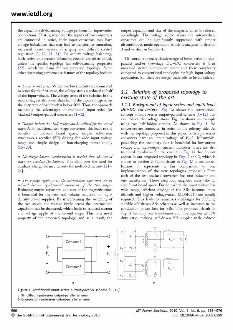
1.1.1 Background of input-series and multi-levelDC–DC converters: Fig. 1a shows the conventionalconcept of input-series output-parallel scheme [1–12] thatcan reduce the voltage stress. Fig. 1b shows an exampleusing two half-bridge circuits. As shown in Fig. 1, theconverters are connected in series on the primary side. Aswith the topology proposed in this paper, both input-seriesconverters have an input voltage of Vin/2. Meanwhile,paralleling the secondary side is beneficial for low-outputvoltage and high-output current. However, there are alsotechnical drawbacks for the circuit in Fig. 1b that do notappear in our proposed topology in Figs. 2 and 3, which isshown in Section 2. (This circuit in Fig. 1b is mentionedbecause it represents a fair comparison to oneimplementation of the new topologies proposed.) First,each of the two stacked converters has one inductor andone transformer. These total four magnetic cores take upsignificant board space. Further, when the input voltage haswide range, efficient driving of the SRs becomes moredifficult and higher voltage-rated MOSFETs are usuallyrequired. This leads to numerous challenges for fulfillingsuitable self-driven SRs schemes as well as increases in theconduction power loss for SRs. The proposed circuit inFig. 3 has only one transformer and this operates at 50%duty ratio, making self-driven SR simpler with reduced
Figure 1 Traditional input-series output-parallel scheme [1–12]
a Simplified input-series output-parallel schemeb Example of input-series output-parallel scheme
IET Power Electron., 2010, Vol. 3, Iss. 6, pp. 965–976doi: 10.1049/iet-pel.2009.0189
IETdo
www.ietdl.org
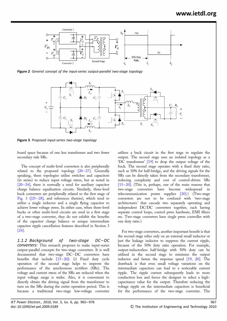
Figure 3 Proposed input-series two-stage topology
Figure 2 General concept of the input-series output-parallel two-stage topology
i
board space because of one less transformer and two fewersecondary side SRs.
The concept of multi-level converters is also peripherallyrelated to the proposed topology [20–27]. Generallyspeaking, these topologies utilise switches and capacitors(in series) to reduce input voltage stress, but as noted in[20–24], there is normally a need for auxiliary capacitorcharge balance equalisation circuits. Similarly, three-levelbuck converters are peripherally related to the first stage ofFig. 3 ([25–28], and references therein), which tend toutilise a single inductor and a single flying capacitor toachieve lower voltage stress. In either case, when three-levelbucks or other multi-level circuits are used in a first stageof a two-stage converter, they do not exhibit the benefitsof the capacitor charge balance or unique intermediatecapacitor ripple cancellation features described in Section 3[24].
1.1.2 Background of two-stage DC – DCconverters: This research proposes to make input-seriesoutput-parallel concepts for two-stage converters. It is welldocumented that two-stage DC–DC converters havebenefits that include [15–20]: (i) Fixed duty cycleoperation of the second stage helps to improve theperformance of the synchronous rectifiers (SRs). Thevoltage and current stress of the SRs are reduced when theinput voltage range is wider. Also, it is convenient todirectly obtain the driving signal from the transformer toturn on the SRs during the entire operation period. This isbecause a traditional two-stage low-voltage converter
Power Electron., 2010, Vol. 3, Iss. 6, pp. 965–976: 10.1049/iet-pel.2009.0189
utilises a buck circuit in the first stage to regulate theoutput. The second stage uses an isolated topology as a‘DC transformer’ [19] to drop the output voltage of thebuck. The second stage operates with a fixed duty ratio,such as 50% for half-bridge, and the driving signals for theSRs can be directly taken from the secondary transformer,reducing complexity and cost of control-driven SRs[15–20]. (This is, perhaps, one of the main reasons thattwo-stage converters have become widespread intelecommunication power supplies [20].) (Two-stageconverters are not to be confused with ‘two-stagearchitectures ’ that cascade two separately operating andindependent DC/DC converters together, each havingseparate control loops, control pwm hardware, EMI filtersetc. Two-stage converters have single pwm controller withone duty ratio.)
For two-stage converters, another important benefit is thatthe second stage relies only on an external small inductor orjust the leakage inductor to suppress the current ripple,because of the 50% duty ratio operation. For example,output-inductorless half-bridge with 50% duty can beutilised in the second stage to minimise the outputinductor and fasten the response speed [19, 20]. Thedrawback is that even small voltage variations on theintermediate capacitors can lead to a noticeable currentripple. The ripple current subsequently leads to moreconduction loss and forces the designer to select a high-capacitance value for the output. Therefore reducing thevoltage ripple on the intermediate capacitors is beneficialfor the performance of the two-stage converter. The
967
& The Institution of Engineering and Technology 2010

96
&
www.ietdl.org
proposed topology in Fig. 3 maintains the benefits of two-stage converters but also has lower voltage ripple because ofthe ripple cancellation benefits discussed in Section 3.
Finally, it is important to mention that neither traditionalinput-series output-parallel converters nor two-stageconverters necessarily claim improved power efficiency overtraditional topologies, such as full bridge. Further, there isincreased component count because of more switches.Thus, there are design trade-offs to consider when using allthese topologies. The benefits of reduced input voltagestress with self-driven SR for wide and high-input voltagerange seem to be the important application area for Fig. 3.
2 Operation principles and design2.1 General principle
Fig. 2 describes the concept of the proposed input-series two-stage topology. Any two non-isolated converters (buck,boost, buck–boost etc.) are input-series connected for thefirst stage to regulate the output voltage, shown in thefigure as Converter 1 and Converter 2 (each with the sameduty ratio). Because of the input-series connection, eachnon-isolated converter in the first stage shares half of theinput voltage. Therefore lower voltage stress is achieved.Interleaved operation is used for the first stage, and voltageripple on the intermediate capacitors can be reduced, asdiscussed in Section 3.
A symmetrically driven transformer is utilised for the secondstage operating at 50% duty ratio, as shown in Fig. 1. Vc is thevoltage across the intermediate capacitors in Fig. 1. Thecandidate topologies of the second stage typically have twoinput capacitors connected in series, such as half-bridge ordual input-series output-parallel. Each intermediate capacitoris connected to the primary winding of the transformer for50% of the time, that is the primary transformer voltage, Vp,is equal to +Vc 50% of the time and 2Vc the other 50% ofthe time. As a result, the voltage balance of the twointermediate capacitors can be automatically regulated by themagnetising inductance of the transformer because ofvoltage-second balance of the inductor. This is a benefit ofthe proposed approach over most multi-level switchingconverters. As noted in [21–24], most multi-level topologiesrequire external circuitry to balance intermediate capacitorvoltages. Further, there are also additional documentedbenefits (from two-stage converters [17–20]) of transformerwaveforms that we further discuss in Section 4.
2.2 Specific series buck + half-bridgeimplementation
For the purpose of illustration, we now focus on one specificimplementation of the concept, as shown in Fig. 3. Fig. 4illustrates the circuit’s related waveforms. Vgs1, Vgs2, Vgs3 andVgs4 are the driving signals for the switches on the primaryside. As can be seen in the figure, the first stage contains
8The Institution of Engineering and Technology 2010
dual interleaved buck converters. One channel consists ofC1, C3, S1, D1 and L1; the other consists of C2, C4, S2, D2
and L2. The intermediate capacitors (C3 and C4) supplythe dual outputs of the first stage, which for this topologywill have self-regulating charge balance. The second stageis an isolated output-inductorless half-bridge, whichconsists of C3, C4, S3, S4, T1, S5, S6 and Lk, with fixedoperation (50% duty ratio). Lk can be an external smallinductor or just the leakage inductance of the transformer.
The purpose of using output-inductorless half-bridge is toreduce the converter’s size as well as improve the response ofthe converter. Since the primary switches of the second stageoperate complementarily, by utilising the energy stored in theleakage inductance (or adding small external inductance),zero-voltage turn-on can be realised for S3 and S4. Fixedduty ratio helps to achieve high efficiency for SRs (S5 andS6). It is convenient to directly obtain the driving signalfrom the transformer to turn on the SRs during the entireoperation period as traditional two-stage circuit does. Also,taking the advantage of the half-bridge circuit, the secondstage keeps the charge balance of the dual intermediatecapacitors. As a result, charge balance of C1 and C2 are alsomaintained. Interval t0−t4 is defined as the switchingperiod T. The lengths of t02t1 and t22t3 are defined asDT, which represents the duty ratio, and thus, the dutyratio D will always be less than one-half.
For the purpose of reducing the voltage ripple across theintermediate capacitors, the first stage operates atdiscontinuous mode. As a result, S1 and S2 have zero-current turn-on. Fig. 5 shows different operation modes ofthe circuit during different periods in one switching cycle.
Figure 4 Waveforms of the proposed topology
IET Power Electron., 2010, Vol. 3, Iss. 6, pp. 965–976doi: 10.1049/iet-pel.2009.0189

Id
www.ietdl.org
Figure 5 Detailed description of the operation principle of the proposed topology
a Interval 1 (t0 –t1)b Interval 2 (t1 –t2)c Interval 3 (t2 – t3)d Interval 4 (t3 –t4)
Eo
For the convenience of description, the short transitiontime of the second stage is not included. Obviously,ZVS for S3 and S4 can be fulfilled during the transitiontime just as traditional circuits [15–20]. The followingdescription explains the detailed operation principle of thistopology.
The length of t0−t1 and t2−t3 are defined as DT, where Drepresents the duty ratio.
Interval 1 (t02t1): The condition of this period is shown inFig. 5a. In this interval, S1 is turned on. The upper buckcircuit transfers energy from C1 to C3 through L1. Thecharging current IL1, which is shown in Fig. 5, increaseslinearly according to L1(dIL1/dt) = (Vin/2) − V1. (V1 is thevoltage across the intermediate capacitors.) At the sametime, the current of the bottom buck circuit, which is IL2,flows through the freewheeling diode D2 and charges C4.The current decreases according to L2(dIL2/dt) = −V1
until zero during this interval. For the second stage, S3 isturned on. The transformer current IT flows through S3.The intermediate capacitor C3 transfers power, the loadthrough the transformer and S6.
Interval 2 (t1–t2): As shown in Fig. 5b, S1 is turned off duringthis interval. Therefore current IL1 goes through thefreewheeling diode D1 and starts to decrease linearlyaccording to L1(dIL1/dt) = −V1, which is shown in Fig. 8.Also, the current of the bottom buck is zero because of thediscontinuous mode operation. The second stage still transfersenergy from C3 to the load through the transformer and S6.
Interval 3 (t2– t3): The condition of this interval, which isshown in Fig. 5c, is similar to interval 1. The two buck
T Power Electron., 2010, Vol. 3, Iss. 6, pp. 965–976i: 10.1049/iet-pel.2009.0189
circuits switch the conditions. During this interval, S2 isturned on. The bottom buck transfers energy from C2 toC4 through L2. Its output current, which is IL2, starts toincrease linearly according to L2(dIL2/dt) = (Vin/2) − V1
through S2 and L2. Also, the current of the upper buck,which is IL1, still flows through the freewheeling diode anddecreases linearly according to L1(dIL1/dt) = −V1 untilzero. In this case, S3 is turned off. The transformer currentIT flows through S4. The power is transferred from C4 tothe secondary side through transformer and S5.
Interval 4 (t3– t4): Fig. 5d shows the condition of the lastinterval. In this case, S2 is turned off. IL2 transfers to thefreewheeling diode and decreases linearly. The current ofthe upper buck is zero because discontinuous modeoperation. Current IT still circulates through S4. Thesecond stage continues transferring energy from C4 to thesecondary side through transformer and S5.
The first stage buck converters operate in discontinuousconduction mode. Thus, their duty ratios are given as
D =������������������������
2L(Id/2)V1
(Vin/2)(Vin/2 − V1)T
√
[16], where Id = (ns/np)Iout; np and ns are the turn number ofthe primary and secondary windings. Ignoring the shorttransition time, the duty ratio of the entire proposed two-stage topology is
D =��������������������������
4L Iout Vo
Vin[Vin − 2Vo(np/ns)]T
√
969
& The Institution of Engineering and Technology 2010
97
&
www.ietdl.org
The non-linear relation between duty ratio and output voltageindicates that control design will be more complicated. In fact,the difficulty of modelling and controlling two-stageconverters is demonstrated in [19, 20] and robust controllerdesign for circuits in Figs. 2 and 3 is an open research topic.
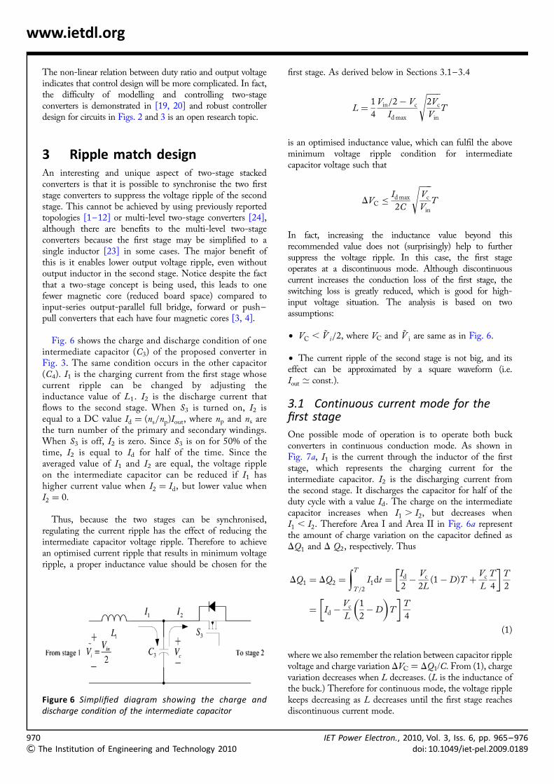
3 Ripple match designAn interesting and unique aspect of two-stage stackedconverters is that it is possible to synchronise the two firststage converters to suppress the voltage ripple of the secondstage. This cannot be achieved by using previously reportedtopologies [1–12] or multi-level two-stage converters [24],although there are benefits to the multi-level two-stageconverters because the first stage may be simplified to asingle inductor [23] in some cases. The major benefit ofthis is it enables lower output voltage ripple, even withoutoutput inductor in the second stage. Notice despite the factthat a two-stage concept is being used, this leads to onefewer magnetic core (reduced board space) compared toinput-series output-parallel full bridge, forward or push–pull converters that each have four magnetic cores [3, 4].
Fig. 6 shows the charge and discharge condition of oneintermediate capacitor (C3) of the proposed converter inFig. 3. The same condition occurs in the other capacitor(C4). I1 is the charging current from the first stage whosecurrent ripple can be changed by adjusting theinductance value of L1. I2 is the discharge current thatflows to the second stage. When S3 is turned on, I2 isequal to a DC value Id = (ns/np)Iout, where np and ns arethe turn number of the primary and secondary windings.When S3 is off, I2 is zero. Since S3 is on for 50% of thetime, I2 is equal to Id for half of the time. Since theaveraged value of I1 and I2 are equal, the voltage rippleon the intermediate capacitor can be reduced if I1 hashigher current value when I2 = Id, but lower value whenI2 = 0.
Thus, because the two stages can be synchronised,regulating the current ripple has the effect of reducing theintermediate capacitor voltage ripple. Therefore to achievean optimised current ripple that results in minimum voltageripple, a proper inductance value should be chosen for the
Figure 6 Simplified diagram showing the charge anddischarge condition of the intermediate capacitor
0The Institution of Engineering and Technology 2010
first stage. As derived below in Sections 3.1–3.4
L = 1
4
Vin/2 − Vc
Id max
����2Vc
Vin
√T
is an optimised inductance value, which can fulfil the aboveminimum voltage ripple condition for intermediatecapacitor voltage such that
DVC ≤ Id max
2C
����Vc
Vin
√T
In fact, increasing the inductance value beyond thisrecommended value does not (surprisingly) help to furthersuppress the voltage ripple. In this case, the first stageoperates at a discontinuous mode. Although discontinuouscurrent increases the conduction loss of the first stage, theswitching loss is greatly reduced, which is good for high-input voltage situation. The analysis is based on twoassumptions:
† VC , V i/2, where VC and V i are same as in Fig. 6.
† The current ripple of the second stage is not big, and itseffect can be approximated by a square waveform (i.e.Iout ≃ const.).
3.1 Continuous current mode for thefirst stage
One possible mode of operation is to operate both buckconverters in continuous conduction mode. As shown inFig. 7a, I1 is the current through the inductor of the firststage, which represents the charging current for theintermediate capacitor. I2 is the discharging current fromthe second stage. It discharges the capacitor for half of theduty cycle with a value Id. The charge on the intermediatecapacitor increases when I1 . I2, but decreases whenI1 , I2. Therefore Area I and Area II in Fig. 6a representthe amount of charge variation on the capacitor defined asDQ1 and D Q2, respectively. Thus
DQ1 = DQ2 =∫T
T/2
I1dt = Id
2− Vc
2L(1 − D)T + Vc
L
T
4
[ ]T
2
= Id −Vc
L
1
2− D
( )T
[ ]T
4
(1)
where we also remember the relation between capacitor ripplevoltage and charge variation DVC ¼ DQ1/C. From (1), chargevariation decreases when L decreases. (L is the inductance ofthe buck.) Therefore for continuous mode, the voltage ripplekeeps decreasing as L decreases until the first stage reachesdiscontinuous current mode.
IET Power Electron., 2010, Vol. 3, Iss. 6, pp. 965–976doi: 10.1049/iet-pel.2009.0189

IETdo
www.ietdl.org
Figure 7 Currents from the circuit in Fig. 6
a Continuous current mode for first stageb Discontinuous current mode I for the first stagec Discontinuous current mode II for the first staged Discontinuous current mode III for the first stage
3.2 Discontinuous current mode I for thefirst stage
Fig. 7b shows the discontinuous current mode I. In this caseI1 . I2 at t = T/2. Similar to the continuous current mode,the charge variation is
DQ1 = DQ2 = LId
V i − Vc
Id
2= LI 2
d
2(V i − Vc)(2)
where V i = Vin/2 is the input voltage to the buck converter.From (2), the voltage ripple still keeps decreasing with thedecreasing of L until the first stage reaches discontinuouscurrent mode II. Thus, lower voltage ripple is obtained inthis mode when compared with continuous current mode.
3.3 Discontinuous current mode II for thefirst stage
Fig. 7c shows the discontinuous current mode II. In this case,Area I or Area II determines the maximum charge variationin one duty cycle. By computing the charge variationseparately, the following equations are obtained
DQ1 = LId
V i − Vc
Id
2= LI 2
d
2(V i − Vc)(3)
DQ2 = 1/(D1 + D2) − 1
1/(D1 + D2)(D1 + D2)T
1
2
Id
D1 + D2
− Id
( )
= 1
2(1 − D1 − D2)2IdT
(4)
From the above equations, DQ1 decreases with the decreasingof L, whereas DQ2 increase when L decreases. Therefore
Power Electron., 2010, Vol. 3, Iss. 6, pp. 965–976i: 10.1049/iet-pel.2009.0189
minimal voltage ripple is obtained when DQ1 = DQ2. Atthat time, DQ3 = DQ4. Since
D1
D1 + D2
= Vc
V i
(5)
V i − Vc
LD1T = Id
D1 + D2
(6)
The value of L can be represented as
L = V i − Vc
Id
D1(D1 + D2)T (7)
Combining (3), (4) and (7), let DQ1 = DQ2, minimal voltageripple is realised when
D1(D1 + D2) = (1 − D1 − D2)2 (8)
3.4 Discontinuous current mode III forthe first stage
Also, the discontinuous current mode III, which is shown inFig. 7d, is checked. This time, Area II determines themaximum charge variation in one duty cycle. Similar to thediscontinuous current mode II, the value of D Q2 can beobtained from (4). DQ2 decreases when L increases. Thus,this mode has higher voltage ripple than discontinuouscurrent mode II has.
3.4.1 Derivation of optimal inductance value:Based on the above analysis, for a constant input voltageand load current, the minimal intermediate voltage ripplecan be obtained when the converter operates indiscontinuous mode II and (8) is satisfied.
971
& The Institution of Engineering and Technology 2010
97
&
www.ietdl.org
If only considering the full load condition, the value of Lcan be obtained by combining (5)–(7)
Lopt =V i Vc
(V i − Vc)Id max
1 −���Vc
V i
√( )2
T (9)
where V i = Vin/2. But considering the total load range (9) isnot the inductance value for minimal ripple.
For a constant L, DQ1 has the maximum value at full loadby using (3). At that time
DQ1 max =LI 2
d max
2(V i − Vc)(10)
On the other hand, DQ2 does not obtain maximum value atfull load. By combining (4)–(6)
DQ2 = 1
2
(V i − Vc)Vc
V iL(1 − D1 − D2)2(D1 + D2)2T (11)
Thus, the maximal Q2 happens when D1 + D2 = (1/2)
DQ2 max =1
32
(V i − Vc)Vc
V iLT 2 (12)
Since the increasing of L results in the increasing of DQ1 max
and the decreasing of DQ2 max, minimal voltage ripple occurswhen DQ1 max = DQ2 max. Thus, the optimised inductancevalue is achieved for a total load range
Lopt =1
4
V i − Vc
Id max
���Vc
V i
√T (13)
If the input voltage Vin has a variation range, the valueof L should be chosen based on the condition of different
2The Institution of Engineering and Technology 2010
Vin. A simple consideration is to determine L when Vin isin the mid-point or perhaps on the nominal input voltageconduction. The implication of using (13) is that thevoltage ripple on the intermediate capacitors can besignificantly reduced. This also leads to the significantreduction of the current ripple on the second stage. As aresult, the size for the output filtering inductor isminimised and the transient response is improved.Specifically, substituting (13) into (10) and using the factthat C . V ¼ Q leads to the capacitor voltage ripple
DVC ≤ Id max
2C·���V
√c
Vin
· T
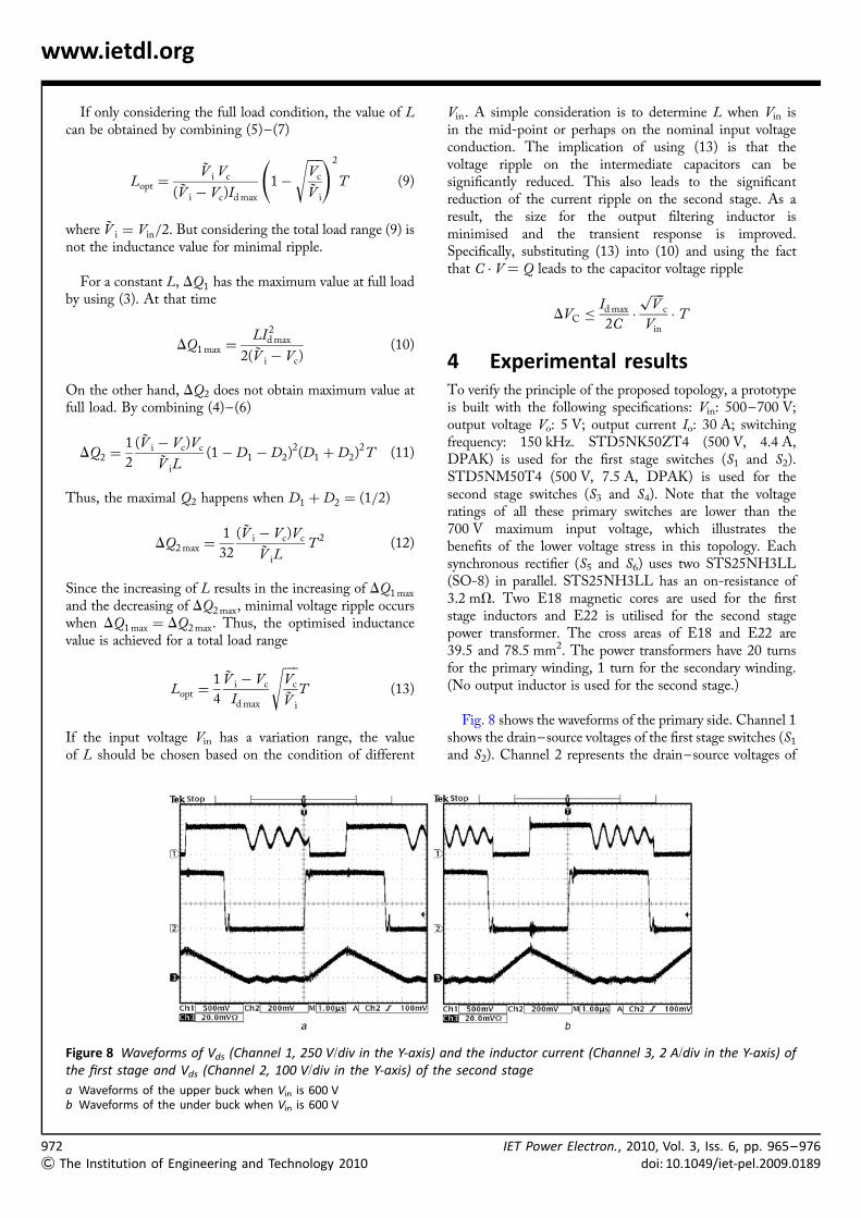
4 Experimental resultsTo verify the principle of the proposed topology, a prototypeis built with the following specifications: Vin: 500–700 V;output voltage Vo: 5 V; output current Io: 30 A; switchingfrequency: 150 kHz. STD5NK50ZT4 (500 V, 4.4 A,DPAK) is used for the first stage switches (S1 and S2).STD5NM50T4 (500 V, 7.5 A, DPAK) is used for thesecond stage switches (S3 and S4). Note that the voltageratings of all these primary switches are lower than the700 V maximum input voltage, which illustrates thebenefits of the lower voltage stress in this topology. Eachsynchronous rectifier (S5 and S6) uses two STS25NH3LL(SO-8) in parallel. STS25NH3LL has an on-resistance of3.2 mV. Two E18 magnetic cores are used for the firststage inductors and E22 is utilised for the second stagepower transformer. The cross areas of E18 and E22 are39.5 and 78.5 mm2. The power transformers have 20 turnsfor the primary winding, 1 turn for the secondary winding.(No output inductor is used for the second stage.)
Fig. 8 shows the waveforms of the primary side. Channel 1shows the drain–source voltages of the first stage switches (S1
and S2). Channel 2 represents the drain–source voltages of
Figure 8 Waveforms of Vds (Channel 1, 250 V/div in the Y-axis) and the inductor current (Channel 3, 2 A/div in the Y-axis) ofthe first stage and Vds (Channel 2, 100 V/div in the Y-axis) of the second stage
a Waveforms of the upper buck when Vin is 600 Vb Waveforms of the under buck when Vin is 600 V
IET Power Electron., 2010, Vol. 3, Iss. 6, pp. 965–976doi: 10.1049/iet-pel.2009.0189

IETdo
www.ietdl.org
Figure 9 Waveforms of Vds (Channel 1, 250 V/div in theY-axis), Vp (Channel 2, 250 V/div in the Y-axis) and theprimary current Ip (Channel 3, 2 A/div in the Y-axis) of thesecond stage and Vds (Channel 4, 20 V/div in the Y-axis) ofthe secondary SR (Vin is 600 V)
Power Electron., 2010, Vol. 3, Iss. 6, pp. 965–976i: 10.1049/iet-pel.2009.0189
the second stage switch (S4). Channel 3 shows the current (I1
or I2) flowing through the first stage inductor. As designed andseen in Fig. 8, the first stage has discontinuous inductorcurrent at full load. As previously explained, this bothreduces the size of the inductor and the switching powerloss. By choosing the optimal inductance value derived as(13), the voltage ripple on the intermediate capacitor can bereduced. Also, it can be clearly seen that the drain–sourcevoltages of S3 and S4 drop to zero before the currents startto increase. Therefore zero-voltage turn-on is fulfilled for thesecond stage switches (S3 and S4). Fig. 9 shows the drain–source voltages of the second stage switch (S4), the voltageacross the primary winding of the transformer, the currentthrough the primary winding of the transformer and thedrain–source voltage of the secondary synchronous rectifier(S5). The current ripple of the second stage is suppressed toa reasonable value although only leakage inductor of thetransformer is utilised for filtering.
We will now experimentally demonstrate the benefits ofoperating the converter in discontinuous mode II, astheoretically demonstrated in Section 3 for the ripple match
Figure 10 Waveforms of Vds (Channel 1, 100 V/div in the Y-axis) of the second stage, voltage ripple on the intermediatecapacitor C3 (Channel 2, 5 V/div in the Y-axis) and the inductor current (Channel 3, 2 A/div in the Y-axis) of the first stage(Vin is 600 V)
a Waveforms in continuous current modeb Waveforms in discontinuous current mode Ic Waveforms in discontinuous current mode IId Waveforms in discontinuous current mode IIINotice how the voltage ripples in Channel 2 are smaller in discontinuous current mode II
973
& The Institution of Engineering and Technology 2010
97
&
www.ietdl.org
design. For the different modes of operation, Fig. 10 showsthe drain–source voltages of the second stage switch (S4),voltage ripple on the intermediate capacitor (C3), thecurrent through the primary winding of the transformerand the inductor current of the first stage. Fig. 10c showsthe lowest ripple voltage across the intermediate capacitorcompared to the three other modes. Using (13), aninductance value of 128 mH is obtained. In thisexperiment, the values of the inductors in the first stage areapproximately: 450 mH for continuous current mode,240 mH for discontinuous current mode I, 128 mH fordiscontinuous current mode II and 68 mH fordiscontinuous current mode III. By comparing the voltageripple across the intermediate capacitor, it can be clearlyseen that minimal voltage ripple is achieved indiscontinuous current mode II. Specifically, even thoughcontinuous current mode inductor is 3.5 times the value asthe 128 mH inductance for discontinuous current mode II,its capacitor peak-to-peak ripple voltage is more than threetimes as much (8 V against 2.5 V). In other words, for thisexample, it would take over three times the inductancevalue to keep the operation in the continuous conductionmode to have the same intermediate bus voltage ripple eventhough the inductance value is already much larger. (Thisvoltage ripple subsequently reflected through thetransformer to the output voltage.) These experimentalresults are in accordance with the (unique to this topology)detailed theoretical analysis on ripple cancellation inSection 3 and demonstrate clear benefits of the approachover prior state of the art, as previously discussed.
Although the conduction loss of the first stage increaseswhen using discontinuous current because of the increasedac current components, the switching loss of the first stageare reduced, since the switches are turned on with zerocurrent. Also, ignoring the effect of the short transitiontime, the size of secondary voltage ripple is directlydetermined by the voltage ripple on the intermediatecapacitors. Since the second stage relies only on the leakageinductor of the transformer to suppress the secondarycurrent ripple, even small voltage variations can lead to anoticeable current ripple. Therefore by operating at theproposed discontinuous current mode II to suppress thevoltage ripple, the conduction power loss of the secondstage (especially the secondary side) can be significantly
4The Institution of Engineering and Technology 2010
reduced. An additional benefit of discontinuous operationis that the first stage has smaller size and quicker transientresponse. By applying the proposed topology in the builtprototype, an efficiency of 88.3% at 600 V input and 5 V/
30 A output is obtained. The efficiency is higher at lowline (89.5% at 500 V input) and decreases to its lowestvalue at high line (87.25% at 700 V input). Although themajor benefits of this topology proposed in this paper arefor reduced voltage ripple and low switch stress, we remarkthat the power efficiency compares favourably to previouslyreported (80–90% in the literature [1–16]) two-stage orseries input power converters – particularly for high-voltageinputs. In summary, the experimental results verify theprinciple and performance of the topology.
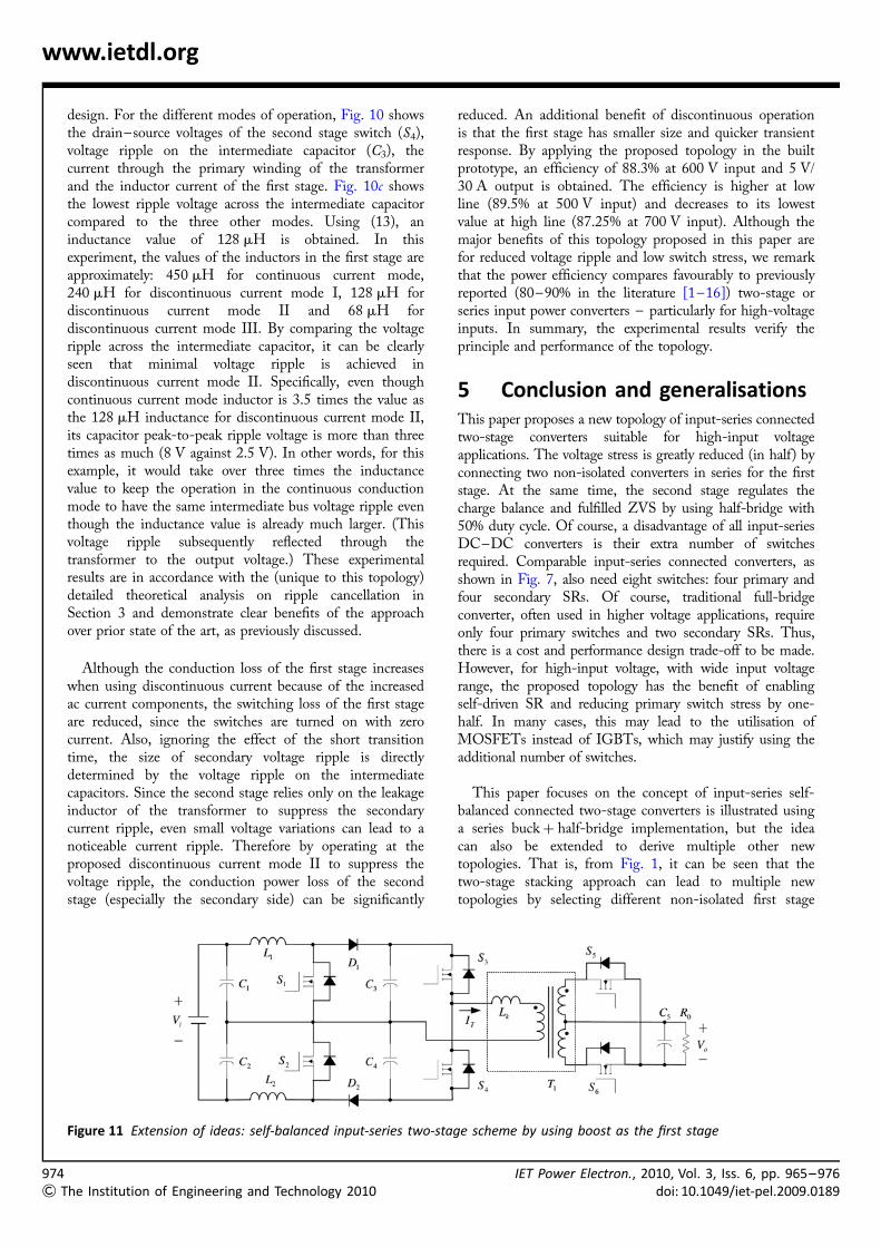
5 Conclusion and generalisationsThis paper proposes a new topology of input-series connectedtwo-stage converters suitable for high-input voltageapplications. The voltage stress is greatly reduced (in half) byconnecting two non-isolated converters in series for the firststage. At the same time, the second stage regulates thecharge balance and fulfilled ZVS by using half-bridge with50% duty cycle. Of course, a disadvantage of all input-seriesDC–DC converters is their extra number of switchesrequired. Comparable input-series connected converters, asshown in Fig. 7, also need eight switches: four primary andfour secondary SRs. Of course, traditional full-bridgeconverter, often used in higher voltage applications, requireonly four primary switches and two secondary SRs. Thus,there is a cost and performance design trade-off to be made.However, for high-input voltage, with wide input voltagerange, the proposed topology has the benefit of enablingself-driven SR and reducing primary switch stress by one-half. In many cases, this may lead to the utilisation ofMOSFETs instead of IGBTs, which may justify using theadditional number of switches.
This paper focuses on the concept of input-series self-balanced connected two-stage converters is illustrated usinga series buck + half-bridge implementation, but the ideacan also be extended to derive multiple other newtopologies. That is, from Fig. 1, it can be seen that thetwo-stage stacking approach can lead to multiple newtopologies by selecting different non-isolated first stage
Figure 11 Extension of ideas: self-balanced input-series two-stage scheme by using boost as the first stage
IET Power Electron., 2010, Vol. 3, Iss. 6, pp. 965–976doi: 10.1049/iet-pel.2009.0189

IETdoi
www.ietdl.org
converters combined with various second stage dual endedisolated converters, such as dual ended forward convertersor push–pull topologies. Also, any non-isolated converterscan be used as the input-series converters, as demonstratedin Fig. 11 with boost converters. Future research willexamine the detailed operation and benefits of these otherspecific topologies. However, conceptually, their methodsare derived from the same concepts presented in this paperderived from Fig. 1: the input voltage is divided into halfby the series capacitor connection. The two boostconverters are connected in such a way that the secondstage half-bridge would operate at 50% duty ratio, whilethe boost converter outputs are regulated.
6 References
[1] GLASER J., WITULSKI A.: ‘Application of a constant-output-power converter in multiple-module converter systems’.IEEE Power Electronics Specialist Conf., June 1992,pp. 909–916
[2] GLASER J., WITULSKI A.: ‘Output plane analysis of load-sharing in multiple-module converter systems, applicationof a constant-output-power converter in multiple-moduleconverter systems’, IEEE Trans. Power Electron., 1994, 9,(1), pp. 43–50
[3] KIM J.-W., YON J.-S., CHO B.H.: ‘Modeling, control, and designof input-series-output-parallel-connected converter forhigh-speed-train power system’, IEEE Trans. Ind. Electron.,2001, 48, (3), pp. 536–544
[4] WANG L., HE X.: ‘Input-series and output-parallelconnection modular DC – DC converters with interleavedconstant duty cycle control strategy’. 33rd Conf. IEEEIndustrial Electronic Society, November 2007,pp. 1901–1906
[5] AYYANAR R., GIRI R., MOHAN N.: ‘Active input-voltage andload-current sharing in input-series and output-parallelconnected modular DC – DC converters using dynamicinput-voltage reference scheme’, IEEE Trans. PowerElectron., 2004, 19, (6), pp. 1462–1473
[6] GIRI R., CHOUDHARY V., AYYANAR R., MOHAN N.: ‘Common-duty-ratio control of input-series connected modular DC – DCconverters with active input voltage and load-currentsharing’, IEEE Trans. Power Electron., 2006, 42, (4),pp. 1101–1111
[7] GRBOVIC P.J.: ‘Master/slave control of input-series- andoutput-parallel-connected converters: concept for low-cost high-voltage auxiliary power supplies’, IEEE Trans.Power Electron., 2009, 24, (2), pp. 316–328
[8] KIMBALL J., MOSSOBA J., KREIN P.: ‘A stabilizing, high-performance controller for input series-output parallel
Power Electron., 2010, Vol. 3, Iss. 6, pp. 965–976: 10.1049/iet-pel.2009.0189
converters’, IEEE Trans. Power Electron., 2008, 23, (3),pp. 1416–1427
[9] VORPERIAN V.: ‘Synthesis of medium voltage dc-to-dcconverters from low-voltage, high-frequency PWMswitching converters’, IEEE Trans. Power Electron., 2007,22, (5), pp. 1619–1635
[10] QIAN T., LEHMAN B.: ‘Dual interleaved active-clampforward with automatic charge balance regulation forhigh input voltage application’, IEEE Trans. PowerElectron., 2008, 23, (1), pp. 38–44
[11] QIAN T., LEHMAN B.: ‘Coupled input-series and output-parallel dual interleaved flyback converter for high inputvoltage application’, IEEE Trans. Power Electron., 2008, 23,(1), pp. 88–95
[12] GLASER J., NASADOSKI J.: ‘A 900 W, 300 V to 50 V dc – dcpower converter with a 30 MHz switching frequency’. IEEEApplied Power Electronics Conf. and Exposition, 2009,pp. 1121–1128
[13] KOO G.-B., MOON G.-W., YOUN M.-J.: ‘Analysis and design ofphase shift full bridge converter with series-connectedtwo transformers’, IEEE Trans. Power Electron., 2004, 19,(2), pp. 411–419
[14] BAGGIO J., HEY H., GRUNDLING H., PINHEIRO H., PINHEIRO J.:‘Isolated interleaved-phase-shift-PWM DC – DC ZVSconverter’, IEEE Trans. Ind. Appl., 2003, 39, (6), pp. 1795–1802
[15] ABE S., YAMAMOTO J., ZAITSU T., NINOMIYA T.: ‘Extension ofbandwidth of two-stage DC – DC converter with low-voltage/high-current output’. IEEE Power ElectronicsSpecialist Conf., 2003, vol. 4, pp. 1593–1598
[16] REN Y., XU M., YAO K., LEE F.: ‘Two-stage 48 V power podexploration for 64-bit microprocessor’. IEEE Applied PowerElectronics Conf. and Exposition, 2003, vol. 1, pp. 426–431
[17] ALOU P., OLIVER J., COBOS J., GARCIA O., UCEDA J.: ‘Buck + halfbridge (d ¼ 50%) topology applied to very low voltagepower converters’. IEEE Applied Power Electronics Conf.and Exposition, 2001, vol. 2, pp. 715–721
[18] MAO H., ABU-QAHOUQ J., LUO S., BATARSEH I.: ‘Zero-voltage-switching (ZVS) two-stage approaches with output currentsharing for 48 V input DC–DC converter’. IEEE Applied PowerElectronics Conf. and Exposition, 2004, vol. 2, pp. 1078–1082
[19] ZHU Y., LEHMAN B.: ‘Control loop design for two-stageDC – DC converters with low voltage/high current output’,IEEE Trans. Power Electron., 2005, 20, (1), pp. 44–55
[20] WANG X., XIAO S., BATARSEH I.: ‘A novel control for two-stageDC/DC converter with fast dynamic response’. IEEE PowerElectronics Specialists Conf., 2004, vol. 1, pp. 43–48
975
& The Institution of Engineering and Technology 2010

97
&
www.ietdl.org
[21] RODRIGUEZ J., LAI J.-S., PENG F.: ‘Multilevel inverters:a survey of topologies, controls, and applications’, IEEETrans. Ind. Electron., 2002, 49, pp. 724–738
[22] PENG F.: ‘A generalized multilevel inverter topology withself voltage balancing’. IEEE Industrial Applications Conf.,2000, pp. 2024–2031
[23] RUAN X., LI B., CHEN Q., TAN S.-C., TSE C.K.: ‘Fundamentalconsiderations of three-level DC – DC converters:topologies, analyses and control’, IEEE Trans. CircuitsSyst.-1, 2008, 55, pp. 3733–3743
[24] ZHU Y., LEHMAN B.: ‘Three-level switching cell for lowvoltage/high-current DC – DC converters’, IEEE Trans.Power Electron., 2007, 22, (5), pp. 1997–2007
6The Institution of Engineering and Technology 2010
[25] YOUSEFZADEH V., ALARCON E., MAKSIMOVIC D.: ‘Three-levelbuck converter for envelope tracking applications’, IEEETrans. Power Electron., 2006, 21, (2), pp. 549–552
[26] MEYNARD T.A., FOCH H.: ‘Multi-level conversion: highvoltage choppers and voltage-source inverters’. IEEE PowerElectronics Specialist Conf., 1992, vol. 1, pp. 397–403
[27] RODRIGUES J.P., BARBI I., PERIN A.J.: ‘Buck converter with ZVSthree level buck clamping’. IEEE Power ElectronicsSpecialists Conf., 2008, pp. 2184–2190
[28] PEREZ-GUERRERO F.F., VENKATESAN K., PATTERSON R.L.: ‘Optimalcontrol of a three level DC to DC buck converter’. IEEEApplied Power Electronics Conf. and Exposition, 14 – 18March 1999, vol. 2, pp. 1006–1009
IET Power Electron., 2010, Vol. 3, Iss. 6, pp. 965–976doi: 10.1049/iet-pel.2009.0189


![ISSN 1755-4535 Three-phase hybrid multilevel … inverter with one high-voltage input dc source and six ... Neutral point clamped ... +1]=127 voltage vectors. 3 Space vector modulation](https://static.fdocuments.net/doc/165x107/5ae44bbd7f8b9a7b218e35a3/issn-1755-4535-three-phase-hybrid-multilevel-inverter-with-one-high-voltage.jpg)


