
ISO154x Low-Power Bidirectional I C Isolators · VCC1 1 8 VCC2 SDA1 2 7 SDA2 SCL1 3 6 SCL2 GND1 4 5...
34
Isolation Capacitor VCC2 VCC1 SDA2 or SCL2 SDA1 or SCL1 GND1 GND2 VREF Product Folder Sample & Buy Technical Documents Tools & Software Support & Community Reference Design An IMPORTANT NOTICE at the end of this data sheet addresses availability, warranty, changes, use in safety-critical applications, intellectual property matters and other important disclaimers. PRODUCTION DATA. ISO1540, ISO1541 SLLSEB6D – JULY 2012 – REVISED DECEMBER 2016 ISO154x Low-Power Bidirectional I 2 C Isolators 1 1 Features 1• Isolated Bidirectional, I 2 C Compatible, Communication • Supports up to 1-MHz Operation • 3-V to 5.5-V Supply Range • Open-Drain Outputs With 3.5-mA Side 1 and 35- mA Side 2 Sink Current Capability • –40°C to +125°C Operating Temperature • ±50-kV/μs Transient Immunity (Typical) • HBM ESD Protection of 4 kV on All Pins; 8 kV on Bus Pins • Safety-Related Certifications: – 4242-V PK Isolation per DIN V VDE V 0884-10 (VDE V 0884-10): 2006-12 – 2500-V RMS Isolation for 1 Minute per UL 1577 – CSA Component Acceptance Notice 5A, IEC 60950-1 and IEC 61010-1 End Equipment Standards – CQC Basic Insulation per GB4943.1-2011 2 Applications • Isolated I 2 C Buses • SMBus and PMBus Interfaces • Open-Drain Networks • Motor Control Systems • Battery Management • I 2 C Level Shifting 3 Description The ISO1540 and ISO1541 devices are low-power, bidirectional isolators that are compatible with I 2 C interfaces. These devices have logic input and output buffers that are separated by Texas Instruments Capacitive Isolation technology using a silicon dioxide (SiO 2 ) barrier. When used with isolated power supplies, these devices block high voltages, isolate grounds, and prevent noise currents from entering the local ground and interfering with or damaging sensitive circuitry. This isolation technology provides for function, performance, size, and power consumption advantages when compared to optocouplers. The ISO1540 and ISO1541 devices enable a complete isolated I 2 C interface to be implemented within a small form factor. The ISO1540 has two isolated bidirectional channels for clock and data lines while the ISO1541 has a bidirectional data and a unidirectional clock channel. The ISO1541 is useful in applications that have a single master while the ISO1540 is suitable for multi- master applications. For applications where clock stretching by the slave is possible, the ISO1540 device should be used. Isolated bidirectional communication is accomplished within these devices by offsetting the low-level output voltage on side 1 to a value greater than the high- level input voltage on side 1, thus preventing an internal logic latch that otherwise would occur with standard digital isolators. Device Information (1) PART NUMBER PACKAGE BODY SIZE (NOM) ISO1540 ISO1541 SOIC (8) 4.90 mm × 3.91 mm (1) For all available packages, see the orderable addendum at the end of the data sheet. Simplified Schematic
Transcript of ISO154x Low-Power Bidirectional I C Isolators · VCC1 1 8 VCC2 SDA1 2 7 SDA2 SCL1 3 6 SCL2 GND1 4 5...

Isol
atio
n C
apac
itor
VCC2VCC1
SDA2or SCL2
SDA1or SCL1
GND1 GND2
VREF
Product
Folder
Sample &Buy
Technical
Documents
Tools &
Software
Support &Community
ReferenceDesign
An IMPORTANT NOTICE at the end of this data sheet addresses availability, warranty, changes, use in safety-critical applications,intellectual property matters and other important disclaimers. PRODUCTION DATA.
ISO1540, ISO1541SLLSEB6D –JULY 2012–REVISED DECEMBER 2016
ISO154x Low-Power Bidirectional I2C Isolators
1
1 Features1• Isolated Bidirectional, I2C Compatible,
Communication• Supports up to 1-MHz Operation• 3-V to 5.5-V Supply Range• Open-Drain Outputs With 3.5-mA Side 1 and 35-
mA Side 2 Sink Current Capability• –40°C to +125°C Operating Temperature• ±50-kV/µs Transient Immunity (Typical)• HBM ESD Protection of 4 kV on All Pins;
8 kV on Bus Pins• Safety-Related Certifications:
– 4242-VPK Isolation per DIN V VDE V 0884-10(VDE V 0884-10): 2006-12
– 2500-VRMS Isolation for 1 Minute per UL 1577– CSA Component Acceptance Notice 5A, IEC
60950-1 and IEC 61010-1 End EquipmentStandards
– CQC Basic Insulation per GB4943.1-2011
2 Applications• Isolated I2C Buses• SMBus and PMBus Interfaces• Open-Drain Networks• Motor Control Systems• Battery Management• I2C Level Shifting
3 DescriptionThe ISO1540 and ISO1541 devices are low-power,bidirectional isolators that are compatible with I2Cinterfaces. These devices have logic input and outputbuffers that are separated by Texas InstrumentsCapacitive Isolation technology using a silicon dioxide(SiO2) barrier. When used with isolated powersupplies, these devices block high voltages, isolategrounds, and prevent noise currents from entering thelocal ground and interfering with or damagingsensitive circuitry.
This isolation technology provides for function,performance, size, and power consumptionadvantages when compared to optocouplers. TheISO1540 and ISO1541 devices enable a completeisolated I2C interface to be implemented within asmall form factor.
The ISO1540 has two isolated bidirectional channelsfor clock and data lines while the ISO1541 has abidirectional data and a unidirectional clock channel.The ISO1541 is useful in applications that have asingle master while the ISO1540 is suitable for multi-master applications. For applications where clockstretching by the slave is possible, the ISO1540device should be used.
Isolated bidirectional communication is accomplishedwithin these devices by offsetting the low-level outputvoltage on side 1 to a value greater than the high-level input voltage on side 1, thus preventing aninternal logic latch that otherwise would occur withstandard digital isolators.
Device Information(1)
PART NUMBER PACKAGE BODY SIZE (NOM)ISO1540ISO1541 SOIC (8) 4.90 mm × 3.91 mm
(1) For all available packages, see the orderable addendum atthe end of the data sheet.
Simplified Schematic

2
ISO1540, ISO1541SLLSEB6D –JULY 2012–REVISED DECEMBER 2016 www.ti.com
Product Folder Links: ISO1540 ISO1541
Submit Documentation Feedback Copyright © 2012–2016, Texas Instruments Incorporated
Table of Contents1 Features .................................................................. 12 Applications ........................................................... 13 Description ............................................................. 14 Revision History..................................................... 25 Pin Configuration and Functions ......................... 46 Specifications......................................................... 5
6.1 Absolute Maximum Ratings ...................................... 56.2 ESD Ratings.............................................................. 66.3 Recommended Operating Conditions....................... 66.4 Thermal Information .................................................. 66.5 Power Ratings........................................................... 66.6 Insulation Specifications............................................ 76.7 Safety-Related Certifications..................................... 86.8 Safety Limiting Values .............................................. 86.9 Electrical Characteristics........................................... 96.10 Supply Current Characteristics ............................. 106.11 Timing Requirements ............................................ 106.12 Switching Characteristics ...................................... 116.13 Insulation Characteristics Curves ......................... 126.14 Typical Characteristics .......................................... 13
7 Parameter Measurement Information ................ 168 Detailed Description ............................................ 18
8.1 Overview ................................................................. 188.2 Functional Block Diagrams ..................................... 188.3 Feature Description................................................. 198.4 Isolator Functional Principle.................................... 198.5 Device Functional Modes........................................ 20
9 Application and Implementation ........................ 219.1 Application Information............................................ 219.2 Typical Application .................................................. 23
10 Power Supply Recommendations ..................... 2511 Layout................................................................... 25
11.1 Layout Guidelines ................................................. 2511.2 Layout Example .................................................... 25
12 Device and Documentation Support ................. 2612.1 Documentation Support ........................................ 2612.2 Related Links ........................................................ 2612.3 Receiving Notification of Documentation Updates 2612.4 Community Resources.......................................... 2612.5 Trademarks ........................................................... 2612.6 Electrostatic Discharge Caution............................ 2612.7 Glossary ................................................................ 26
13 Mechanical, Packaging, and OrderableInformation ........................................................... 27
4 Revision HistoryNOTE: Page numbers for previous revisions may differ from page numbers in the current version.
Changes from Revision C (June 2015) to Revision D Page
• Deleted the Device Comparison Table; see the Features List table for device comparison ................................................ 4• Changed the status of CQC certification from planned to certified ....................................................................................... 8• Changed the Regulatory Information table to Safety-Related Certifications and updated content........................................ 8• Changed formatting of supply current parameters to combine device and sides. Moved parameters to separate table ... 10• Added the Receiving Notification of Documentation Updates section ................................................................................ 26
Changes from Revision B (May 2013) to Revision C Page
• Added Pin Configuration and Functions section, ESD Ratings table, Feature Description section, Device FunctionalModes, Application and Implementation section, Power Supply Recommendations section, Layout section, Deviceand Documentation Support section, and Mechanical, Packaging, and Orderable Information section .............................. 1
• VDE Standard changed to DIN V VDE V 0884-10 (VDE V 0884-10): 2006-12 .................................................................... 1• Changed minimum air gap (Clearance) parameter, L(I01), to external clearance, CLR, and minimum external
tracking (creepage) parameter, L(I02), to external creepage................................................................................................. 7• Changed values and test conditions in the Insulation Specifications table ............................................................................ 7• Changed the descriptions of VDE and CSA information ....................................................................................................... 8
Changes from Revision A (October 2012) to Revision B Page
• Change Safety Feature From: (VDE 0884 Part 2) (Pending) To: (VDE 0884 Part 2) (Approved)......................................... 1• Changed, VDE column From: File number: 40016131 (pending) To: File number: 40016131.............................................. 8

3
ISO1540, ISO1541www.ti.com SLLSEB6D –JULY 2012–REVISED DECEMBER 2016
Product Folder Links: ISO1540 ISO1541
Submit Documentation FeedbackCopyright © 2012–2016, Texas Instruments Incorporated
Changes from Original (July 2012) to Revision A Page
• Changed From: CSA Component Acceptance Notice 5A (Pending) To: CSA Component Acceptance Notice 5A(Approved) .............................................................................................................................................................................. 1
• Changed From: IEC 60950-1 and IEC 61010-1 End Equipment Standards (Pending) To: IEC 60950-1 and IEC61010-1 End Equipment Standards (Approved)..................................................................................................................... 1
• Changed Safety-Related Certifications, CSA column From: File number: 220991 (pending) To: File number: 220991....... 8

1VCC1 8 VCC2
2SDA1 7 SDA2
3SCL1 6 SCL2
4GND1 5 GND2
Not to scale
Isol
atio
n
Side 2Side 1
4
ISO1540, ISO1541SLLSEB6D –JULY 2012–REVISED DECEMBER 2016 www.ti.com
Product Folder Links: ISO1540 ISO1541
Submit Documentation Feedback Copyright © 2012–2016, Texas Instruments Incorporated
5 Pin Configuration and Functions
ISO1540 D Package8-Pin SOICTop View
Pin Functions—ISO1540PIN
I/O DESCRIPTIONNAME NO.GND1 4 — Ground, side 1GND2 5 — Ground, side 2SCL1 3 I/O Serial clock input / output, side 1SCL2 6 I/O Serial clock input / output, side 2SDA1 2 I/O Serial data input / output, side 1SDA2 7 I/O Serial data input / output, side 2VCC1 1 — Supply voltage, side 1VCC2 8 — Supply voltage, side 2

1VCC1 8 VCC2
2SDA1 7 SDA2
3SCL1 6 SCL2
4GND1 5 GND2
Not to scale
Isol
atio
n
Side 2Side 1
5
ISO1540, ISO1541www.ti.com SLLSEB6D –JULY 2012–REVISED DECEMBER 2016
Product Folder Links: ISO1540 ISO1541
Submit Documentation FeedbackCopyright © 2012–2016, Texas Instruments Incorporated
ISO1541 D Package8-Pin SOICTop View
Pin Functions—ISO1541PIN
I/O DESCRIPTIONNAME NO.GND1 4 — Ground, side 1GND2 5 — Ground, side 2SCL1 3 I Serial clock input, side 1SCL2 6 O Serial clock output, side 2SDA1 2 I/O Serial data input / output, side 1SDA2 7 I/O Serial data input / output, side 2VCC1 1 — Supply voltage, side 1VCC2 8 — Supply voltage, side 2
(1) Stresses beyond those listed under Absolute Maximum Ratings may cause permanent damage to the device. These are stress ratingsonly, which do not imply functional operation of the device at these or any other conditions beyond those indicated under RecommendedOperating Conditions. Exposure to absolute-maximum-rated conditions for extended periods may affect device reliability.
(2) All voltage values here within are with respect to the local ground pin (GND1 or GND2) and are peak voltage values.(3) Maximum voltage must not exceed 6 V.
6 Specifications
6.1 Absolute Maximum Ratingsover operating free-air temperature range (unless otherwise noted) (1) (2)
MIN MAX UNIT
VoltageVCC1, VCC2 –0.5 6
VSDA1, SCL1 –0.5 VCC1 + 0.5 (3)
SDA2, SCL2 –0.5 VCC2 + 0.5 (3)
IO Output currentSDA1, SCL1 –20 20
mASDA2, SCL2 –100 100
TJ(MAX) Maximum junction temperature 150 °CTstg Storage temperature –65 150 °C

6
ISO1540, ISO1541SLLSEB6D –JULY 2012–REVISED DECEMBER 2016 www.ti.com
Product Folder Links: ISO1540 ISO1541
Submit Documentation Feedback Copyright © 2012–2016, Texas Instruments Incorporated
(1) JEDEC document JEP155 states that 500-V HBM allows safe manufacturing with a standard ESD control process.(2) JEDEC document JEP157 states that 250-V CDM allows safe manufacturing with a standard ESD control process.
6.2 ESD RatingsVALUE UNIT
V(ESD) Electrostatic discharge
Human body model (HBM), per ANSI/ESDA/JEDECJS-001 (1)
Bus pins ±8000
VAll pins ±4000
Charged-device model (CDM), per JEDEC specification JESD22-C101 (2)
±1500
Machine Model JEDEC JESD22-A115-A, all pins ±200
(1) This represents the maximum frequency with the maximum bus load (C) and the maximum current sink (IO). If the system has less buscapacitance, then higher frequencies can be achieved.
6.3 Recommended Operating ConditionsMIN MAX UNIT
VCC1, VCC2 Supply voltage 3 5.5 VVSDA1, VSCL1 Input and output signal voltages, side 1 0 VCC1 VVSDA2, VSCL2 Input and output signal voltages, side 2 0 VCC2 VVIL1 Low-level input voltage, side 1 0 0.5 VVIH1 High-level input voltage, side 1 0.7 × VCC1 VCC1 VVIL2 Low-level input voltage, side 2 0 0.3 × VCC2 VVIH2 High-level input voltage, side 2 0.7 × VCC2 VCC2 VIOL1 Output current, side 1 0.5 3.5 mAIOL2 Output current, side 2 0.5 35 mAC1 Capacitive load, side 1 40 pFC2 Capacitive load, side 2 400 pFfMAX Operating frequency (1) 1 MHzTA Ambient temperature –40 125 °CTJ Junction temperature –40 136 °CTSD Thermal shutdown 139 171 °C
(1) For more information about traditional and new thermal metrics, see the Semiconductor and IC Package Thermal Metrics applicationreport (SPRA953).
6.4 Thermal Information
THERMAL METRIC (1)ISO154x
UNITD (SOIC)8 PINS
RθJA Junction-to-ambient thermal resistance 114.6 °C/WRθJC(top) Junction-to-case (top) thermal resistance 69.6 °C/WRθJB Junction-to-board thermal resistance 55.3 °C/WψJT Junction-to-top characterization parameter 27.2 °C/WψJB Junction-to-board characterization parameter 54.7 °C/WRθJC(bot) Junction-to-case (bottom) thermal resistance N/A °C/W
6.5 Power RatingsPARAMETER TEST CONDITIONS MIN TYP MAX UNIT
PD Maximum power dissipation (both sides) VCC1 = VCC2 = 5.5 V, TJ = 150 °C, C1 =40 pF, C2 = 400 pF;Input a 1-MHz 50% duty cycle clock signal
85 mWPD1 Maximum power dissipation (side-1) 34 mWPD2 Maximum power dissipation (side-2) 51 mW

7
ISO1540, ISO1541www.ti.com SLLSEB6D –JULY 2012–REVISED DECEMBER 2016
Product Folder Links: ISO1540 ISO1541
Submit Documentation FeedbackCopyright © 2012–2016, Texas Instruments Incorporated
(1) Creepage and clearance requirements should be applied according to the specific equipment isolation standards of an application. Careshould be taken to maintain the creepage and clearance distance of a board design to ensure that the mounting pads of the isolator onthe printed-circuit board do not reduce this distance. Creepage and clearance on a printed-circuit board become equal in certain cases.Techniques such as inserting grooves and/or ribs on a printed circuit board are used to help increase these specifications.
(2) This coupler is suitable for basic electrical insulation only within the maximum operating ratings. Compliance with the safety ratings shallbe ensured by means of suitable protective circuits.
(3) Apparent charge is electrical discharge caused by a partial discharge (pd).(4) All pins on each side of the barrier tied together creating a two-terminal device
6.6 Insulation SpecificationsPARAMETER TEST CONDITIONS VALUE UNIT
GENERALCLR External clearance (1) Shortest terminal-to-terminal distance through air >4 mm
CPG External creepage (1) Shortest terminal-to-terminal distance across thepackage surface >4 mm
DTI Distance through the insulation Minimum internal gap (internal clearance) 0.014 mmCTI Comparative tracking index DIN EN 60112 (VDE 0303-11); IEC 60112 >400 V
Material group II
Overvoltage categoryRated mains voltage ≤ 150 VRMS I–IVRated mains voltage ≤ 300 VRMS I–III
DIN V VDE V 0884-10 (VDE V 0884-10):2006-12 (2)
VIORM Maximum repetitive peak isolation voltage AC voltage (bipolar) 566 VPK
VIOTM Maximum transient isolation voltageVTEST = VIOTMt = 60 s (qualification)t = 1 s (100% production)
4242 VPK
qpd Apparent charge (3)
Method a: After I/O safety test subgroup 2/3, Vini =VIOTM, tini = 60 s; Vpd(m) = 1.2 × VIORM = 680 VPK, tm= 10 s
<5
pCMethod a: After environmental tests subgroup 1,Vini = VIOTM, tini = 60 s; Vpd(m) = 1.6 × VIORM = 906VPK, tm = 10 s
<5
Method b1: At routine test (100% production) andpreconditioning (type test) Vini = VIOTM, tini = 1 s;Vpd(m) = 1.875 × VIORM = 1062 VPK, tm = 1 s
<5
CIO Barrier capacitance, input to output (4) VIO = 0.4 sin (2πft), f = 1 MHz ~1 pF
RIO Isolation resistance, input to output (4)
VIO = 500 V, TA = 25°C >1012
ΩVIO = 500 V, 100°C ≤ TA ≤ 125°C >1011
VIO = 500 V at TS = 150°C >109
Pollution degree 2Climatic category 40/125/21
UL 1577
VISO Withstand isolation voltageVTEST = VISO = 2500 VRMS, t = 60 s (qualification);VTEST = 1.2 × VISO = 3000 VRMS, t = 1 s (100%production)
2500 VRMS

8
ISO1540, ISO1541SLLSEB6D –JULY 2012–REVISED DECEMBER 2016 www.ti.com
Product Folder Links: ISO1540 ISO1541
Submit Documentation Feedback Copyright © 2012–2016, Texas Instruments Incorporated
6.7 Safety-Related CertificationsVDE CSA UL CQC
Certified according to DIN V VDE V0884-10 (VDE V 0884-10):2006-12and DIN EN 61010-1
Approved under CSAComponent Acceptance Notice5A, CSA/IEC 60950-1, andCSA/IEC 61010-1
Recognized under UL 1577Component RecognitionProgram
Certified according to GB4943.1-2011
Basic InsulationMaximum Transient Overvoltage,4242 VPK;Maximum Repetitive Peak Voltage,566 VPK
2.8-kVRMS Insulation Rating; 400VRMS Basic Insulation workingvoltage per CSA 60950-1-07+A1+A2 and IEC 60950-1 2ndEd.+A1+A2;300 VRMS Basic, 150 VRMSReinforced Insulation workingvoltage per CSA 61010-1-12 andIEC 61010-1 3rd Ed.,
Single protection, 2500 VRMS
Basic Insulation, Altitude ≤ 5000m, Tropical Climate, 250 VRMSmaximum working voltage
Certificate number: 40016131 Master contract number: 220991 File number: E181974 Certificate number:CQC14001109540
6.8 Safety Limiting ValuesSafety limiting intends to minimize potential damage to the isolation barrier upon failure of input or output circuitry. A failure ofthe I/O can allow low resistance to ground or the supply and, without current limiting, dissipate sufficient power to overheatthe die and damage the isolation barrier, potentially leading to secondary system failures.
PARAMETER TEST CONDITIONS MIN TYP MAX UNIT
ISSafety input, output, or supplycurrent
RθJA = 114.6°C/W, VI = 5.5 V, TJ = 150°C, TA = 25°C,see Figure 1 198
mARθJA = 114.6°C/W, VI = 3.6 V, TJ = 150°C, TA = 25°C,see Figure 1 303
TS Safety temperature 150 °C
The safety-limiting constraint is the maximum junction temperature specified in the data sheet. The powerdissipation and junction-to-air thermal impedance of the device installed in the application hardware determinesthe junction temperature. The assumed junction-to-air thermal resistance in the Thermal Information table is thatof a device installed on a high-K test board for leaded surface-mount packages. The power is the recommendedmaximum input voltage times the current. The junction temperature is then the ambient temperature plus thepower times the junction-to-air thermal resistance.

9
ISO1540, ISO1541www.ti.com SLLSEB6D –JULY 2012–REVISED DECEMBER 2016
Product Folder Links: ISO1540 ISO1541
Submit Documentation FeedbackCopyright © 2012–2016, Texas Instruments Incorporated
(1) This parameter does not apply to the ISO1541 SCL1 line as it is unidirectional.(2) ∆VOIT1 = VOL1 – VIHT1. This represents the minimum difference between a Low-Level Output Voltage and a High-Level Input Voltage
Threshold to prevent a permanent latch condition that would otherwise exist with bidirectional communication.(3) Any VCC voltages, on either side, less than the minimum will ensure device lockout. Both VCC voltages greater than the maximum will
prevent device lockout.
6.9 Electrical Characteristicsover recommended operating conditions, unless otherwise noted
PARAMETER TEST CONDITIONS MIN TYP MAX UNITSIDE 1 (ONLY)
VILT1Voltage input threshold low, SDA1and SCL1 500 550 660 mV
VIHT1Voltage input threshold high, SDA1and SCL1 540 610 700 mV
VHYST1 Voltage input hysteresis VIHT1 –VILT1 40 60 mV
VOL1Low-level output voltage, SDA1and SCL1 (1) 0.5 mA ≤ (ISDA1 and ISCL1) ≤ 3.5 mA 650 800 mV
ΔVOIT1
Low-level output voltage to high-level input voltage thresholddifference, SDA1 and SCL1 (1) (2)
0.5 mA ≤ (ISDA1 and ISCL1) ≤ 3.5 mA 50 mV
SIDE 2 (ONLY)
VILT2Voltage input threshold low, SDA2and SCL2 0.3 × VCC2 0.4 × VCC2 V
VIHT2Voltage input threshold high, SDA2and SCL2 0.4 × VCC2 0.5 × VCC2 V
VHYST2 Voltage input hysteresis VIHT2 – VILT2 0.05 × VCC2 V
VOL2Low-level output voltage, SDA2and SCL2 0.5 mA ≤ (ISDA2 and ISCL2) ≤ 35 mA 0.4 V
BOTH SIDES
|II|Input leakage currents, SDA1,SCL1, SDA2, and SCL2
VSDA1, VSCL1 = VCC1;VSDA2, VSCL2 = VCC2 0.01 10 µA
CIInput capacitance to local ground,SDA1, SCL1, SDA2, and SCL2 VI = 0.4 × sin(2E6πt) + 2.5 V 7 pF
CMTI Common-mode transient immunity See Figure 21 25 50 kV/µs
VCCUVVCC undervoltage lockoutthreshold (3) 2.1 2.5 2.8 V

10
ISO1540, ISO1541SLLSEB6D –JULY 2012–REVISED DECEMBER 2016 www.ti.com
Product Folder Links: ISO1540 ISO1541
Submit Documentation Feedback Copyright © 2012–2016, Texas Instruments Incorporated
6.10 Supply Current Characteristicsover recommended operating conditions, unless otherwise noted. For more information, see Figure 19.
PARAMETER TEST CONDITIONS MIN TYP MAX UNIT3 V ≤ VCC1, VCC2 ≤ 3.6 V
ICC1 Supply current, side 1
ISO1540
VSDA1, VSCL1 = GND1; VSDA2, VSCL2 = GND2;R1, R2 = Open; C1, C2 = Open 2.4 3.6
mA
VSDA1, VSCL1 = VCC1; VSDA2, VSCL2 = VCC2;R1, R2 = Open; C1, C2 = Open 2.5 3.8
ISO1541
VSDA1, VSCL1 = GND1; VSDA2, VSCL2 = GND2;R1, R2 = Open; C1, C2 = Open 2.1 3.3
VSDA1, VSCL1 = VCC1; VSDA2, VSCL2 = VCC2;R1, R2 = Open; C1, C2 = Open 2.3 3.6
ICC2 Supply current, side 2 ISO1540 andISO1541
VSDA1, VSCL1 = GND1; VSDA2, VSCL2 = GND2;R1, R2 = Open; C1, C2 = Open 1.7 2.7
mAVSDA1, VSCL1 = VCC1; VSDA2, VSCL2 = VCC2;R1, R2 = Open; C1, C2 = Open 1.9 3.1
4.5 V ≤ VCC1, VCC2 ≤ 5.5 V
ICC1 Supply current, side 1
ISO1540
VSDA1, VSCL1 = GND1; VSDA2, VSCL2 = GND2;R1,R2 = Open; C1,C2 = Open 3.1 4.7
mA
VSDA1, VSCL1 = VCC1; VSDA2, VSCL2 = VCC2;R1, R2 = Open; C1, C2 = Open 3.1 4.7
ISO1541
VSDA1, VSCL1 = GND1; VSDA2, VSCL2 = GND2;R1, R2 = Open; C1, C2 = Open 2.8 4.4
VSDA1, VSCL1 = VCC1; VSDA2, VSCL2 = VCC2;R1, R2 = Open; C1, C2 = Open 2.9 4.5
ICC2 Supply current, side 2 ISO1540 andISO1541
VSDA1, VSCL1 = GND1; VSDA2, VSCL2 = GND2;R1, R2 = Open; C1, C2 = Open 2.3 3.7
mAVSDA1, VSCL1 = VCC1; VSDA2, VSCL2 = VCC2;R1, R2 = Open; C1, C2 = Open 2.5 4
6.11 Timing RequirementsMIN NOM MAX UNIT
tSP Input noise filter 5 12 nstUVLO Time to recover from UVLO 2.7 V to 0.9 V; See Figure 22 30 50 110 µs

11
ISO1540, ISO1541www.ti.com SLLSEB6D –JULY 2012–REVISED DECEMBER 2016
Product Folder Links: ISO1540 ISO1541
Submit Documentation FeedbackCopyright © 2012–2016, Texas Instruments Incorporated
(1) This parameter does not apply to the ISO1541 SCL1 line as it is unidirectional.
6.12 Switching Characteristicsover recommended operating conditions, unless otherwise noted
PARAMETER TEST CONDITIONS MIN TYP MAX UNIT3 V ≤ VCC1, VCC2 ≤ 3.6 V
tf1Output Signal Fall Time(SDA1, SCL1)
See Figure 19R1 = 953 Ω,C1 = 40 pF
0.7 × VCC1 to 0.3 × VCC1 8 17 29ns
0.9 × VCC1 to 900 mV 16 29 48
tf2Output Signal Fall Time(SDA2, SCL2)
See Figure 19R2 = 95.3 Ω,C2 = 400 pF
0.7 × VCC2 to 0.3 × VCC2 14 23 47ns
0.9 × VCC2 to 400 mV 35 50 100
tpLH1-2Low-to-High PropagationDelay, Side 1 to Side 2
See Figure 19R1 = 953 Ω,R2 = 95.3 Ω,C1, C2 = 10 pF
0.55 V to 0.7 × VCC2 33 65 ns
tPHL1-2High-to-Low PropagationDelay, Side 1 to Side 2 0.7 V to 0.4 V 90 181 ns
PWD1-2Pulse Width Distortion|tpHL1-2 – tpLH1-2| 55 123 ns
tPLH2-1(1) Low-to-High Propagation
Delay, Side 2 to Side 1 0.4 × VCC2 to 0.7 × VCC1 47 68 ns
tPHL2-1(1) High-to-Low Propagation
Delay, Side 2 to Side 1 0.4 × VCC2 to 0.9 V 67 109 ns
PWD2-1(1) Pulse Width Distortion
|tpHL2-1 – tpLH2-1| 20 49 ns
tLOOP1(1) Round-trip propagation
delay on Side 1
See Figure 20;R1 = 953 Ω, C1 = 40 pFR2 = 95.3 Ω, C2 = 400 pF
0.4 V to 0.3 × VCC1 100 165 ns
4.5 V ≤ VCC1, VCC2 ≤ 5.5 V
tf1Output Signal Fall Time(SDA1, SCL1)
See Figure 19R1 = 1430 Ω,C1 = 40 pF
0.7 × VCC1 to 0.3 × VCC1 6 11 20ns
0.9 × VCC1 to 900 mV 13 21 39
tf2Output Signal Fall Time(SDA2, SCL2)
See Figure 19R2 = 143 Ω,C2 = 400 pF
0.7 × VCC2 to 0.3 × VCC2 10 18 35ns
0.9 × VCC2 to 400 mV 28 41 76
tpLH1-2Low-to-High PropagationDelay, Side 1 to Side 2
See Figure 19R1 = 1430 Ω,R2 = 143 Ω,C1,2 = 10 pF
0.55 V to 0.7 × VCC2 31 62 ns
tPHL1-2High-to-Low PropagationDelay, Side 1 to Side 2 0.7 V to 0.4 V 70 139 ns
PWD1-2Pulse Width Distortion|tpHL1-2 – tpLH1-2| 38 80 ns
tPLH2-1(1) Low-to-high propagation
delay, side 2 to side 1 0.4 × VCC2 to 0.7 × VCC1 55 80 ns
tPHL2-1(1) High-to-low propagation
delay, Side 2 to side 1 0.4 × VCC2 to 0.9 V 47 85 ns
PWD2-1(1) Pulse Width Distortion
|tpHL2-1 – tpLH2-1| 8 21 ns
tLOOP1(1) Round-trip propagation
delay on side 1
See Figure 20;R1 = 1430 Ω, C1 = 40 pFR2 = 143 Ω, C2 = 400 pF
0.4 V to 0.3 × VCC1 110 180 ns

Ambient Temperature (qC)
Saf
ety
Lim
iting
Cur
rent
(m
A)
0 50 100 150 2000
50
100
150
200
250
300
350VCC1 = VCC2 = 3.6 VVCC1 = VCC2 = 5.5 V
12
ISO1540, ISO1541SLLSEB6D –JULY 2012–REVISED DECEMBER 2016 www.ti.com
Product Folder Links: ISO1540 ISO1541
Submit Documentation Feedback Copyright © 2012–2016, Texas Instruments Incorporated
6.13 Insulation Characteristics Curves
Figure 1. Thermal Derating Curve for Limiting Current per VDE

Free-Air Temperature (qC)
Fal
l Tim
e t f2
(ns
)
-40 -25 -10 5 20 35 50 65 80 95 110 1250
5
10
15
20
25
30
D003
R2 = 95.3 :R2 = 2.2 k:
Free-Air Temperature (qC)
Fal
l Tim
e t f2
(ns
)
-40 -25 -10 5 20 35 50 65 80 95 110 1250
5
10
15
20
25
30
D004
R2 = 143 :R2 = 2.2 k:
Free-Air Temperature (qC)
Fal
l Tim
e, t f
1 (n
s)
-40 -25 -10 5 20 35 50 65 80 95 110 1250
2
4
6
8
10
12
14
16
18
20
D001
R1= 953 :R1= 2.2 k:
Free-Air Temperature (qC)
Fal
l Tim
e, t f
1 (n
s)
-40 -25 -10 5 20 35 50 65 80 95 110 1250
2
4
6
8
10
12
14
16
18
20
D002
R1 = 1430 :R1 = 2.2 k:
Ou
tpu
t V
olta
ge
, V
(V)
OL
1
0.780
0.740
0.800
0.720
0.680
0.760
0.660
0.640
0.600
0.700
0.620
I = 3.5 mAOL1
I = 0.5 mAOL1
−40 −25 −10 5 20 35 50 65 80 95 110 125
Free−Air Temperature (°C)
0 0.3 0.6 0.9
Outp
ut C
urr
ent, I
(mA
)O
L1
Applied Voltage, V , V (V)SDA1 SCL1
0.1 0.2 0.4 0.5 0.7 0.8
-0.5
1.0
0.0
2.0
0.5
3.0
1.5
2.5
13
ISO1540, ISO1541www.ti.com SLLSEB6D –JULY 2012–REVISED DECEMBER 2016
Product Folder Links: ISO1540 ISO1541
Submit Documentation FeedbackCopyright © 2012–2016, Texas Instruments Incorporated
6.14 Typical Characteristics
Figure 2. Side 1: Output Low Voltage vs Free-AirTemperature
TA = 25°C
Figure 3. Side 1: Output Low Current vs SDA1 or SCL1Applied Voltage
VCC1 = 3.3 V C1 = 40 pFFall time measured from 70% to 30% VCC1
Figure 4. Side 1: Output Fall Time vs Free-Air Temperature
VCC1 = 5 V C1 = 40 pFFall time measured from 70% to 30% VCC1
Figure 5. Side 1: Output Fall Time vs Free-air Temperature
VCC2 = 3.3 V C2 = 400 pFFall time measured from 70% to 30% VCC2
Figure 6. Side 2: Output Fall Time vs Free-Air Temperature
VCC2 = 5 V C2 = 400 pFFall time measured from 70% to 30% VCC2
Figure 7. Side 2: Output Fall Time vs Free-Air Temperature

Free-Air Temperature (qC)
Pro
paga
tion
Del
ay, t
PH
L2-1
(ns
)
-40 -25 -10 5 20 35 50 65 80 95 110 1250
10
20
30
40
50
60
70
D009
VCC1 and VCC2 = 3.3 V, R1 = 953 :VCC1 and VCC2 = 5 V, R1 = 1430 :
Free-Air Temperature (qC)
Pro
paga
tion
Del
ay, t
PH
L2-1
(ns
)
-40 -25 -10 5 20 35 50 65 80 95 110 1250
10
20
30
40
50
60
70
80
D010
VCC1 and VCC2 = 3.3 V, R1 = 953 :VCC1 and VCC2 = 5 V, R1 = 1430 :
Free-Air Temperature (qC)
Pro
paga
tion
Del
ay, t
PLH
1-2
(ns)
-40 -25 -10 5 20 35 50 65 80 95 110 1251000
1005
1010
1015
1020
1025
1030
1035
1040
1045
1050
D007
VCC1 and VCC2 = 3.3 VVCC1 and VCC2 = 5 V
Free-Air Temperature (qC)
Pro
paga
tion
Del
ay, t
PH
L1-2
(ns
)
-40 -25 -10 5 20 35 50 65 80 95 110 1250
10
20
30
40
50
60
70
80
90
D008
VCC1 and VCC2 = 3.3 VVCC1 and VCC2 = 5 V
Free-Air Temperature (qC)
Pro
paga
tion
Del
ay, t
PLH
1-2 (
ns)
-40 -25 -10 5 20 35 50 65 80 95 110 1250
5
10
15
20
25
30
35
40
45
D005
VCC1 and VCC2 = 3.3 V, R2 = 95.3 :VCC1 and VCC2 = 5 V, R2 = 143 :
Free-Air Temperature (qC)
Pro
paga
tion
Del
ay, t
PH
L1-2
(ns
)
-40 -25 -10 5 20 35 50 65 80 95 110 1250
20
40
60
80
100
120
D006
VCC1 and VCC2 = 3.3 V, R2 = 95.3 :VCC1 and VCC2 = 5 V, R2 = 143 :
14
ISO1540, ISO1541SLLSEB6D –JULY 2012–REVISED DECEMBER 2016 www.ti.com
Product Folder Links: ISO1540 ISO1541
Submit Documentation Feedback Copyright © 2012–2016, Texas Instruments Incorporated
Typical Characteristics (continued)
C2 = 10 pF
Figure 8. tPLH1-2 Propagation Delay vs Free-Air Temperature
C2 = 10 pF
Figure 9. tPHL1-2 Propagation Delay vs Free-Air Temperature
R2 = 2.2 kΩ C2 = 400 pF
Figure 10. tPLH1-2 Propagation Delay vs Free-AirTemperature
R2 = 2.2 kΩ C2 = 400 pF
Figure 11. tPHL1-2 Propagation Delay vs Free-AirTemperature
C1 = 10 pF
Figure 12. tPLH2-1 Propagation Delay vs Free-AirTemperature
C1 = 10 pF
Figure 13. tPHL2-1 Propagation Delay vs Free-AirTemperature

Free-Air Temperature (qC)
Com
mon
-Mod
e T
rans
ient
Imm
unity
(kV
/Ps)
-40 -25 -10 5 20 35 50 65 80 95 110 1250
10
20
30
40
50
60
70
D015
VCC1 and VCC2 = 3.3 VVCC1 and VCC2 = 5 V
Free-Air Temperature (qC)
t LO
OP
1 (n
s)
-40 -25 -10 5 20 35 50 65 80 95 110 1250
20
40
60
80
100
120
140
D013
VCC1 and VCC2 = 3.3 V, R1 = 953 :, R2 = 95.3 :VCC1 and VCC2 = 5 V, R1 = 1430 :, R2 = 143 :
Free-Air Temperature (qC)
t LO
OP
1 (n
s)
-40 -25 -10 5 20 35 50 65 80 95 110 125575
580
585
590
595
600
D014
VCC1 and VCC2 = 3.3 VVCC1 and VCC2 = 5 V
0
10
20
30
40
50
60
70
80
−40 −25 −10 5 20 35 50 65 80 95 110 125
Free-Air Temperature (°C)
Pro
pa
ga
tio
n D
ela
y,t P
HL2-1
(ns)
VCC1 and VCC2 = 3.3 V
VCC1 and VCC2 = 5 V
Free-Air Temperature (qC)
Pro
paga
tion
Del
ay, t
PLH
2-1
(ns)
-40 -25 -10 5 20 35 50 65 80 95 110 125132
134
136
138
140
142
144
146
148
D011
VCC1 and VCC2 = 3.3 VVCC1 and VCC2 = 5 V
15
ISO1540, ISO1541www.ti.com SLLSEB6D –JULY 2012–REVISED DECEMBER 2016
Product Folder Links: ISO1540 ISO1541
Submit Documentation FeedbackCopyright © 2012–2016, Texas Instruments Incorporated
Typical Characteristics (continued)
R1 = 2.2 kΩ C1 = 40 pF
Figure 14. tPLH2-1 Propagation Delay vs Free-AirTemperature
R1 = 2.2 kΩ C1 = 40 pF
Figure 15. tPHL2-1 Propagation Delay vs Free-AirTemperature
C1 = 40 pF C2 = 400 pF
Figure 16. tLOOP1 vs Free-Air Temperature
C1 = 40 pF C2 = 400 pFR1 = 2.2 kΩ R2 = 2.2 kΩ
Figure 17. tLOOP1 vs Free-Air Temperature
Figure 18. CMTI vs Free-Air Temperature

VCMTI
Input
+
Output
GNDx GNDy
VCCx VCCy
Isol
atio
n
2 k 2 k
±
GND1VCC1 R1
VCC1
C1
GND1
SDA1 or SCL1Output
Isol
atio
n
VCC2
0.4 V
0.3 VCC1tLOOP1
SDA1SCL1 (ISO1540 Only)
Copyright © 2016, Texas Instruments Incorporated
SDA1
SCL1SCL2
SDA2
C1 C1 C2 C2
R1 R1 R2 R2
±
+ ±
+ VCC2VCC1
ISO1540ISO1541
Copyright © 2016, Texas Instruments Incorporated
16
ISO1540, ISO1541SLLSEB6D –JULY 2012–REVISED DECEMBER 2016 www.ti.com
Product Folder Links: ISO1540 ISO1541
Submit Documentation Feedback Copyright © 2012–2016, Texas Instruments Incorporated
7 Parameter Measurement Information
Figure 19. Test Diagram
Figure 20. tLoop1 Setup and Timing Diagram
Figure 21. Common-Mode Transient Immunity Test Circuit

Isola
tio
n
+
Output
-
GNDx GNDy
VCCx
Ry
VCCy
Isola
tion
SDAx or
SCLx
+
Output
GNDx GNDy
VCCx
Ry
VCCy
0 V
Side x, Side y VCCx,VCCy Ry
1, 2 3.3 V, 3.3 V 95.3 Ω
2, 1 3.3 V, 3.3 V 953 Ω
or
SDAx or
SCLx
VCCx or
VCCy
Output
2 .7 V
0.9 V
tUVLO
VCCy
0 V
VCCx
17
ISO1540, ISO1541www.ti.com SLLSEB6D –JULY 2012–REVISED DECEMBER 2016
Product Folder Links: ISO1540 ISO1541
Submit Documentation FeedbackCopyright © 2012–2016, Texas Instruments Incorporated
Parameter Measurement Information (continued)
Figure 22. tUVLO Test Circuit and Timing Diagrams
SDA2
SCL1 SCL2
GND2GND1
VCC2VCC1
SDA1
VREF
Isol
atio
n C
apac
itor
VREF
18
ISO1540, ISO1541SLLSEB6D –JULY 2012–REVISED DECEMBER 2016 www.ti.com
Product Folder Links: ISO1540 ISO1541
Submit Documentation Feedback Copyright © 2012–2016, Texas Instruments Incorporated
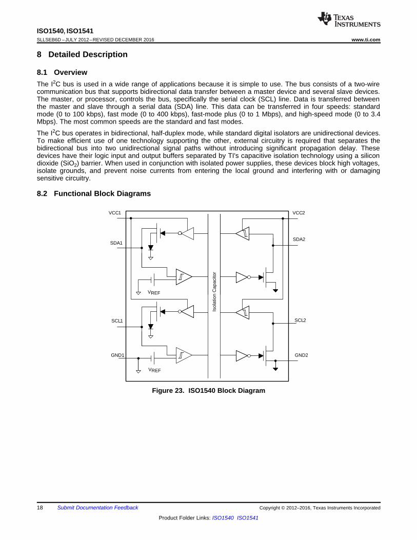
8 Detailed Description
8.1 OverviewThe I2C bus is used in a wide range of applications because it is simple to use. The bus consists of a two-wirecommunication bus that supports bidirectional data transfer between a master device and several slave devices.The master, or processor, controls the bus, specifically the serial clock (SCL) line. Data is transferred betweenthe master and slave through a serial data (SDA) line. This data can be transferred in four speeds: standardmode (0 to 100 kbps), fast mode (0 to 400 kbps), fast-mode plus (0 to 1 Mbps), and high-speed mode (0 to 3.4Mbps). The most common speeds are the standard and fast modes.
The I2C bus operates in bidirectional, half-duplex mode, while standard digital isolators are unidirectional devices.To make efficient use of one technology supporting the other, external circuitry is required that separates thebidirectional bus into two unidirectional signal paths without introducing significant propagation delay. Thesedevices have their logic input and output buffers separated by TI's capacitive isolation technology using a silicondioxide (SiO2) barrier. When used in conjunction with isolated power supplies, these devices block high voltages,isolate grounds, and prevent noise currents from entering the local ground and interfering with or damagingsensitive circuitry.
8.2 Functional Block Diagrams
Figure 23. ISO1540 Block Diagram

VSDA1
VC-out
VILT1 VIHT1 VOL1
40 mV
RPU1 RPU2
VCC1 VCC2
SDA1
GND1GND2
SDA2
VREF
A
B
D
C
ISO1540
50 mVCbus
Cnode
Copyright © 2016, Texas Instruments Incorporated
SDA2
SCL1 SCL2
GND2GND1
VCC2VCC1
SDA1
VREF
Isol
atio
n C
apac
itor
19
ISO1540, ISO1541www.ti.com SLLSEB6D –JULY 2012–REVISED DECEMBER 2016
Product Folder Links: ISO1540 ISO1541
Submit Documentation FeedbackCopyright © 2012–2016, Texas Instruments Incorporated
Functional Block Diagrams (continued)
(1) See Safety-Related Certifications for detailed Isolation specifications.
Figure 24. ISO1541 Block Diagram
8.3 Feature DescriptionThe device enables a complete isolated I2C interface to be implemented within a small form factor having thefeatures listed in Table 1.
Table 1. Features ListPART NUMBER CHANNEL DIRECTION RATED ISOLATION (1) MAXIMUM FREQUENCY
ISO1540 Bidirectional (SCL)Bidirectional (SDA) 2500 VRMS
4242 VPK1 MHz
ISO1541 Unidirectional (SCL)Bidirectional (SDA)
8.4 Isolator Functional PrincipleTo isolate a bidirectional signal path (SDA or SCL), the ISO1540 internally splits a bidirectional line into twounidirectional signal lines, each of which is isolated through a single-channel digital isolator. Each channel outputis made open-drain to comply with the open-drain technology of I2C. Side 1 of the ISO1540 connects to a low-capacitance I2C node, while side 2 is designed for connecting to a fully loaded I2C bus with up to 400 pF ofcapacitance.
Figure 25. SDA Channel Design and Voltage Levels at SDA1

VOL1
VIHT1
SDA1
SDA2
SDA2
SDA1
TransmitDelay
TransmitDelay
ReceiveDelay
VIHT2
50%
50%
30%
30%
ReceiveDelay
ReceiveDelay
VCC1VCC1VCC2VCC2
VCC1 VCC1 VCC2 VCC2
20
ISO1540, ISO1541SLLSEB6D –JULY 2012–REVISED DECEMBER 2016 www.ti.com
Product Folder Links: ISO1540 ISO1541
Submit Documentation Feedback Copyright © 2012–2016, Texas Instruments Incorporated
Isolator Functional Principle (continued)At first sight, the arrangement of the internal buffers suggests a closed signal loop that is prone to latch-up.However, this loop is broken by implementing an output buffer (B) whose output low-level is raised by a diodedrop to approximately 0.75 V, and the input buffer (C) that consists of a comparator with defined hysteresis. Thecomparator’s upper and lower input thresholds then distinguish between the proper low-potential of 0.4 V(maximum) driven directly by SDA1 and the buffered output low-level of B.
Figure 26 demonstrate the switching behavior of the I2C isolator, ISO1540, between a master node at SDA1 anda heavy loaded bus at SDA2.
Figure 26. SDA Channel Timing in Receive and Transmit Directions
8.4.1 Receive Direction (Left Diagram of Figure 26)When the I2C bus drives SDA2 low, SDA1 follows after a certain delay in the receive path. The output low is thebuffered output of VOL1 = 0.75 V, which is sufficiently low to be detected by Schmitt-trigger inputs with a minimuminput-low voltage of VIL = 0.9 V at 3 V supply levels.
When SDA2 is released, its voltage potential increases towards VCC2 following the time-constant formed byRPU2 and Cbus. After the receive delay, SDA1 is released and also rises towards VCC1, following the time-constant RPU1 × Cnode. Because of the significant lower time-constant, SDA1 may reach VCC1 before SDA2reaches VCC2 potential.
8.4.2 Transmit Direction (Right Diagram of Figure 26)When a master drives SDA1 low, SDA2 follows after a certain delay in the transmit direction. When SDA2 turnslow it also causes the output of buffer B to turn low but at a higher 0.75 V level. This level cannot be observedimmediately as it is overwritten by the lower low-level of the master.
However, when the master releases SDA1, the voltage potential increases and first must pass the upper inputthreshold of the comparator, VIHT1, to release SDA2. SDA1 then increases further until it reaches the bufferedoutput level of VOL1 = 0.75 V, maintained by the receive path. When comparator C turns high, SDA2 is releasedafter the delay in transmit direction. It takes another receive delay until B’s output turns high and fully releasesSDA1 to move toward VCC1 potential.
8.5 Device Functional ModesTable 2 lists the ISO154x functional modes.
(1) H = High Level; L = Low Level; Z = High Impedance or Float; X = Irrelevant; ? = Indeterminate(2) Invalid input condition as an I2C system requires that a pullup resistor to VCC is connected.
Table 2. Function Table (1)
POWER STATE INPUT OUTPUTVCC1 or VCC2 < 2.1 V X Z
VCC1 and VCC2 > 2.8 V L LVCC1 and VCC2 > 2.8 V H ZVCC1 and VCC2 > 2.8 V Z (2) ?

SDA
SCL
VDD
RPU RPU RPU RPU RPU RPU RPU RPU
�CMaster
�CSlave
GND GND GND
SDA SCL
GND
SDA SCL SDA SCL SDA SCL
DACSlave
ADCSlave
21
ISO1540, ISO1541www.ti.com SLLSEB6D –JULY 2012–REVISED DECEMBER 2016
Product Folder Links: ISO1540 ISO1541
Submit Documentation FeedbackCopyright © 2012–2016, Texas Instruments Incorporated
9 Application and Implementation
NOTEInformation in the following applications sections is not part of the TI componentspecification, and TI does not warrant its accuracy or completeness. TI’s customers areresponsible for determining suitability of components for their purposes. Customers shouldvalidate and test their design implementation to confirm system functionality.
9.1 Application Information
9.1.1 I2C Bus OverviewThe inter-integrated circuit (I2C) bus is a single-ended, multi-master, 2-wire bus for efficient inter-ICcommunication in half-duplex mode.
I2C uses open-drain technology, requiring two lines, serial data (SDA) and serial clock (SCL), to be connected toVDD by resistors (see Figure 27). Pulling the line to ground is considered a logic zero while letting the line float isa logic one. This logic is used as a channel access method. Transitions of logic states must occur while the SCLpin is low. Transitions while the SCL pin is high indicate START and STOP conditions. Typical supply voltagesare 3.3 V and 5 V, although systems with higher or lower voltages are allowed.
Figure 27. I2C Bus
I2C communication uses a 7-bit address space with 16 reserved addresses, so a theoretical maximum of 112nodes can communicate on the same bus. In praxis, however, the number of nodes is limited by the specified,total bus capacitance of 400 pF, which restricts communication distances to a few meters.
The specified signaling rates for the ISO1540 and ISO1541 devices are 100 kbps (standard mode), 400 kbps(fast mode), 1 Mbps (fast mode plus).
The bus has two roles for nodes: master and slave. A master node issues the clock and slave addresses, andalso initiates and ends data transactions. A slave node receives the clock and addresses and responds torequests from the master. Figure 28 shows a typical data transfer between master and slave.

From Master to Slave
From Slave to Master
S Slave Address R A DATA A DATA A P
S Slave Address W A DATA A DATA A P
Master Transmitter writing to Slave Receiver
Master Receiver reading from Slave Transmitter
A = acknowledge
A = not acknowledge
S = Start
P = Stop
R = Read
W = Write
1 - 7 1 - 88 9 9 1 - 8 9
SDA
SCL
S P
START
Condition
STOP
condition
7-bit
ADDRESS
8-bit
DATA
8-bit
DATAR/W
ACK /
NACKACK ACK
22
ISO1540, ISO1541SLLSEB6D –JULY 2012–REVISED DECEMBER 2016 www.ti.com
Product Folder Links: ISO1540 ISO1541
Submit Documentation Feedback Copyright © 2012–2016, Texas Instruments Incorporated
Application Information (continued)
Figure 28. Timing Diagram of a Complete Data Transfer
The master initiates a transaction by creating a START condition, following by the 7-bit address of the slave itwishes to communicate with. This is followed by a single read and write (R/W) bit, representing whether themaster wishes to write to 0, or to read from 1 the slave. The master then releases the SDA line to allow the slaveto acknowledge the receipt of data.
The slave responds with an acknowledge bit (ACK) by pulling the SDA pin low during the entire high time of the9th clock pulse on the SCL signal, after which the master continues in either transmit or receive mode (accordingto the R/W bit sent), while the slave continues in the complementary mode (receive or transmit, respectively).
The address and the 8-bit data bytes are sent most significant bit (MSB) first. The START bit is indicated by ahigh-to-low transition of SDA while SCL is high. The STOP condition is created by a low-to-high transition of SDAwhile SCL is high.
If the master writes to a slave, it repeatedly sends a byte with the slave sending an ACK bit. In this case, themaster is in master-transmit mode and the slave is in slave-receive mode.
If the master reads from a slave, it repeatedly receives a byte from the slave, while acknowledging (ACK) thereceipt of every byte but the last one (see Figure 29). In this situation, the master is in master-receive mode andthe slave is in slave-transmit mode.
The master ends the transmission with a STOP bit, or may send another START bit to maintain bus control forfurther transfers.
Figure 29. Transmit or Receive Mode Changes During a Data Transfer
When writing to a slave, a master mainly operates in transmit-mode and only changes to receive-mode whenreceiving acknowledgment from the slave.
When reading from a slave, the master starts in transmit-mode and then changes to receive-mode after sendinga READ request (R/W bit = 1) to the slave. The slave continues in the complementary mode until the end of atransaction.
NOTEThe master ends a reading sequence by not acknowledging (NACK) the last bytereceived. This procedure resets the slave state machine and allows the master to sendthe STOP command.

VCC1 VCC2
GND1 GND2
8
7
4 54
XOUT
XIN
5
6
2
MSP430
G2132
1
2
3
DVss
DVcc
0.1 μF0.1 μF 0.1 μF
6
SDA
SCL
9
8
10 μF
VS
0.1 μF
MBR0520L
MBR0520L
1:2.20.1 μF
3
1
D2
SN6501
D1
Vcc
4,5
2
GND
3.3V
IN
ON GND
OUT1 5
23
LP2981-50 10 μF
10 μF
SDA2SDA1
SCL1 SCL2
1.5 kΩ 1.5 kΩ 1. kΩ5 1. kΩ5
0.1 μF
8
VDD
GND
AIN0
2
1
9
10
SDA
SCL
4
ADDR
ADS 1115
AIN3RDY
3
4 Analog
Inputs
7
VIN
GND
VOUT
26
4REF5040
1μF22 μF
4
VDD
V AOUT
V DOUT
V HREF
V LREF
11
10
SDA
SCL
1
DAC8574
8GND
6
12 3
A2
15
IOVDD
5
4 Analog
Outputs
A3
16
A0
13
9
14
LDAC
A1
0.1 μF
5VISO
5VISO
5VISO5VISO
SD
A
SC
LISO-BARRIER
1Ω
Copyright © 2016, Texas Instruments Incorporated
ISO1541
23
ISO1540, ISO1541www.ti.com SLLSEB6D –JULY 2012–REVISED DECEMBER 2016
Product Folder Links: ISO1540 ISO1541
Submit Documentation FeedbackCopyright © 2012–2016, Texas Instruments Incorporated
9.2 Typical ApplicationIn Figure 30, the ultra low-power microcontroller, MSP430G2132, controls the I2C data traffic of configurationdata and conversion results for the analog inputs and outputs. Low-power data converters build the analoginterface to sensors and actuators. The ISO1541 device provides the required isolation between different groundpotentials of the system controller, remote sensor, and actuator circuitry to prevent ground loop currents thatotherwise may falsify the acquired data.
The entire circuit operates from a single 3.3-V supply. A low-power push-pull converter, SN6501, drives a center-tapped transformer with an output that is rectified and linearly regulated to provide a stable 5-V supply for thedata converter.
Figure 30. Isolated I2C Data Acquisition System
9.2.1 Design RequirementsThe recommended power supply voltages (VCC1 and VCC2) must be from 3 V to 5.5 V. A recommendeddecoupling capacitor with a value of 0.1 µF is required between both the VCC1 and GND1 pins, and the VCC2and GND2 pins to support of power supply voltages transient and to ensure reliable operation at all data rates.
9.2.2 Detailed Design ProcedureThe power-supply capacitor with a value of 0.1-µF must be placed as close to the power supply pins as possible.The recommended placement of the capacitors must be 2-mm maximum from input and output power supplypins (VCC1 and VCC2).
The maximum load permissible on the input lines, SDA1 and SCL1, is ≤ 40 pF and on the output lines, SDA2and SCL2, is ≤ 400 pF.
The minimum pullup resistors on the input lines, SDA1 and SCL1 to VCC1 must be selected in such a way thatinput current drawn is ≤ 3.5 mA. The minimum pullup resistors on the input lines, SDA2 and SCL2, to VCC2 mustbe selected in such a way that output current drawn is ≤ 35 mA. The maximum pullup resistors on the input lines(SDA1 and SCL1) to VCC1 and on output lines (SDA1 and SCL1) to VCC2, depends on the load and rise timerequirements on the respective lines.

T = 25 C
VCC1 = 3.6 V
A
o
Time - 50 ns/div
50
0 m
V/d
iv
900 mV
VOL1
GND1
1
ISO1541
SDA2
SCL2SCL1
GND2GND1
VCC2VCC1
SDA1
Isol
atio
n C
apac
itor
4
Side 1 Side 2
2mm maximum
2 mm maximum
8
7
6
5
2
3
1
1 k 10 �F 10 �F
1 k 1 k 1 k
Copyright © 2016, Texas Instruments Incorporated
1
ISO1540
SDA2
SCL2SCL1
GND2GND1
VCC2VCC1
SDA1
Isol
atio
n C
apac
itor
4
Side 1 Side 2
2mm maximum
2 mm maximum
8
7
6
5
2
3
1
1 k 10 �F 10 �F
1 k 1 k 1 k
Copyright © 2016, Texas Instruments Incorporated
24
ISO1540, ISO1541SLLSEB6D –JULY 2012–REVISED DECEMBER 2016 www.ti.com
Product Folder Links: ISO1540 ISO1541
Submit Documentation Feedback Copyright © 2012–2016, Texas Instruments Incorporated
Typical Application (continued)
Figure 31. Typical ISO1540 Circuit Hookup
Figure 32. Typical ISO1541 Circuit Hookup
9.2.3 Application Curve
Figure 33. Side 1: Low-to-High Transition

10 mils
10 mils
40 milsFR-4
0r ~ 4.5
Keep this
space free
from planes,
traces, pads,
and vias
Ground plane
Power plane
Low-speed traces
High-speed traces
25
ISO1540, ISO1541www.ti.com SLLSEB6D –JULY 2012–REVISED DECEMBER 2016
Product Folder Links: ISO1540 ISO1541
Submit Documentation FeedbackCopyright © 2012–2016, Texas Instruments Incorporated
10 Power Supply RecommendationsTo help ensure reliable operation at data rates and supply voltages, TI recommends connecting a 0.1-µF bypasscapacitor at the input and output supply pins (VCC1 and VCC2). The capacitors should be placed as close to thesupply pins as possible. If only a single, primary-side power supply is available in an application, isolated powercan be generated for the secondary-side with the help of a transformer driver such as TI's SN6501 device. Forsuch applications, detailed power supply design and transformer selection recommendations are available inSN6501 Transformer Driver for Isolated Power Supplies. (SLLSEA0).
11 Layout
11.1 Layout GuidelinesA minimum of four layers is required to accomplish a low EMI PCB design (see Figure 34). Layer stacking shouldbe in the following order (top-to-bottom): high-speed signal layer, ground plane, power plane and low-frequencysignal layer.• Routing the high-speed traces on the top layer avoids the use of vias (and the introduction of their
inductances) and allows for clean interconnects between the isolator and the transmitter and receiver circuitsof the data link.
• Placing a solid ground plane next to the high-speed signal layer establishes controlled impedance fortransmission line interconnects and provides an excellent low-inductance path for the return current flow.
• Placing the power plane next to the ground plane creates additional high-frequency bypass capacitance ofapproximately 100 pF/in2.
• Routing the slower speed control signals on the bottom layer allows for greater flexibility as these signal linksusually have margin to tolerate discontinuities such as vias.
If an additional supply voltage plane or signal layer is needed, add a second power or ground plane system tothe stack to keep it symmetrical. This makes the stack mechanically stable and prevents it from warping. Also thepower and ground plane of each power system can be placed closer together, thus increasing the high-frequencybypass capacitance significantly.
For detailed layout recommendations, see the Digital Isolator Design Guide (SLLA284)
11.1.1 PCB MaterialFor digital circuit boards operating at less than 150 Mbps, (or rise and fall times greater than 1 ns), and tracelengths of up to 10 inches, use standard FR-4 UL94V-0 printed circuit board. This PCB is preferred over cheaperalternatives because of lower dielectric losses at high frequencies, less moisture absorption, greater strength andstiffness, and the self-extinguishing flammability-characteristics.
11.2 Layout Example
Figure 34. Recommended Layer Stack

26
ISO1540, ISO1541SLLSEB6D –JULY 2012–REVISED DECEMBER 2016 www.ti.com
Product Folder Links: ISO1540 ISO1541
Submit Documentation Feedback Copyright © 2012–2016, Texas Instruments Incorporated
12 Device and Documentation Support
12.1 Documentation Support
12.1.1 Related DocumentationFor related documentation see the following:• Digital Isolator Design Guide (SLLA284)• ISO154xEVM Low-Power Bidirectional I2C Isolators Evaluation Module (SLLU166)• TI Isolation Glossary (SLLA353)• SN6501 Transformer Driver for Isolated Power Supplies. (SLLSEA0)
12.2 Related LinksThe table below lists quick access links. Categories include technical documents, support and communityresources, tools and software, and quick access to sample or buy.
Table 3. Related Links
PARTS PRODUCT FOLDER SAMPLE & BUY TECHNICALDOCUMENTS
TOOLS &SOFTWARE
SUPPORT &COMMUNITY
ISO1540 Click here Click here Click here Click here Click hereISO1541 Click here Click here Click here Click here Click here
12.3 Receiving Notification of Documentation UpdatesTo receive notification of documentation updates, navigate to the device product folder on ti.com. In the upperright corner, click on Alert me to register and receive a weekly digest of any product information that haschanged. For change details, review the revision history included in any revised document.
12.4 Community ResourcesThe following links connect to TI community resources. Linked contents are provided "AS IS" by the respectivecontributors. They do not constitute TI specifications and do not necessarily reflect TI's views; see TI's Terms ofUse.
TI E2E™ Online Community TI's Engineer-to-Engineer (E2E) Community. Created to foster collaborationamong engineers. At e2e.ti.com, you can ask questions, share knowledge, explore ideas and helpsolve problems with fellow engineers.
Design Support TI's Design Support Quickly find helpful E2E forums along with design support tools andcontact information for technical support.
12.5 TrademarksE2E is a trademark of Texas Instruments.All other trademarks are the property of their respective owners.
12.6 Electrostatic Discharge CautionThis integrated circuit can be damaged by ESD. Texas Instruments recommends that all integrated circuits be handled withappropriate precautions. Failure to observe proper handling and installation procedures can cause damage.
ESD damage can range from subtle performance degradation to complete device failure. Precision integrated circuits may be moresusceptible to damage because very small parametric changes could cause the device not to meet its published specifications.
12.7 GlossarySLYZ022 — TI Glossary.
This glossary lists and explains terms, acronyms, and definitions.

27
ISO1540, ISO1541www.ti.com SLLSEB6D –JULY 2012–REVISED DECEMBER 2016
Product Folder Links: ISO1540 ISO1541
Submit Documentation FeedbackCopyright © 2012–2016, Texas Instruments Incorporated
13 Mechanical, Packaging, and Orderable InformationThe following pages include mechanical, packaging, and orderable information. This information is the mostcurrent data available for the designated devices. This data is subject to change without notice and revision ofthis document. For browser-based versions of this data sheet, refer to the left-hand navigation.

PACKAGE OPTION ADDENDUM
www.ti.com 15-Apr-2017
Addendum-Page 1
PACKAGING INFORMATION
Orderable Device Status(1)
Package Type PackageDrawing
Pins PackageQty
Eco Plan(2)
Lead/Ball Finish(6)
MSL Peak Temp(3)
Op Temp (°C) Device Marking(4/5)
Samples
HPA02222DR ACTIVE SOIC D 8 2500 Green (RoHS& no Sb/Br)
CU NIPDAU Level-2-260C-1 YEAR -40 to 125 IS1540
ISO1540D ACTIVE SOIC D 8 75 Green (RoHS& no Sb/Br)
CU NIPDAU Level-2-260C-1 YEAR -40 to 125 IS1540
ISO1540DR ACTIVE SOIC D 8 2500 Green (RoHS& no Sb/Br)
CU NIPDAU Level-2-260C-1 YEAR -40 to 125 IS1540
ISO1541D ACTIVE SOIC D 8 75 Green (RoHS& no Sb/Br)
CU NIPDAU Level-2-260C-1 YEAR -40 to 125 IS1541
ISO1541DR ACTIVE SOIC D 8 2500 Green (RoHS& no Sb/Br)
CU NIPDAU Level-2-260C-1 YEAR -40 to 125 IS1541
(1) The marketing status values are defined as follows:ACTIVE: Product device recommended for new designs.LIFEBUY: TI has announced that the device will be discontinued, and a lifetime-buy period is in effect.NRND: Not recommended for new designs. Device is in production to support existing customers, but TI does not recommend using this part in a new design.PREVIEW: Device has been announced but is not in production. Samples may or may not be available.OBSOLETE: TI has discontinued the production of the device.
(2) Eco Plan - The planned eco-friendly classification: Pb-Free (RoHS), Pb-Free (RoHS Exempt), or Green (RoHS & no Sb/Br) - please check http://www.ti.com/productcontent for the latest availabilityinformation and additional product content details.TBD: The Pb-Free/Green conversion plan has not been defined.Pb-Free (RoHS): TI's terms "Lead-Free" or "Pb-Free" mean semiconductor products that are compatible with the current RoHS requirements for all 6 substances, including the requirement thatlead not exceed 0.1% by weight in homogeneous materials. Where designed to be soldered at high temperatures, TI Pb-Free products are suitable for use in specified lead-free processes.Pb-Free (RoHS Exempt): This component has a RoHS exemption for either 1) lead-based flip-chip solder bumps used between the die and package, or 2) lead-based die adhesive used betweenthe die and leadframe. The component is otherwise considered Pb-Free (RoHS compatible) as defined above.Green (RoHS & no Sb/Br): TI defines "Green" to mean Pb-Free (RoHS compatible), and free of Bromine (Br) and Antimony (Sb) based flame retardants (Br or Sb do not exceed 0.1% by weightin homogeneous material)
(3) MSL, Peak Temp. - The Moisture Sensitivity Level rating according to the JEDEC industry standard classifications, and peak solder temperature.
(4) There may be additional marking, which relates to the logo, the lot trace code information, or the environmental category on the device.
(5) Multiple Device Markings will be inside parentheses. Only one Device Marking contained in parentheses and separated by a "~" will appear on a device. If a line is indented then it is a continuationof the previous line and the two combined represent the entire Device Marking for that device.

PACKAGE OPTION ADDENDUM
www.ti.com 15-Apr-2017
Addendum-Page 2
(6) Lead/Ball Finish - Orderable Devices may have multiple material finish options. Finish options are separated by a vertical ruled line. Lead/Ball Finish values may wrap to two lines if the finishvalue exceeds the maximum column width.
Important Information and Disclaimer:The information provided on this page represents TI's knowledge and belief as of the date that it is provided. TI bases its knowledge and belief on informationprovided by third parties, and makes no representation or warranty as to the accuracy of such information. Efforts are underway to better integrate information from third parties. TI has taken andcontinues to take reasonable steps to provide representative and accurate information but may not have conducted destructive testing or chemical analysis on incoming materials and chemicals.TI and TI suppliers consider certain information to be proprietary, and thus CAS numbers and other limited information may not be available for release.
In no event shall TI's liability arising out of such information exceed the total purchase price of the TI part(s) at issue in this document sold by TI to Customer on an annual basis.
OTHER QUALIFIED VERSIONS OF ISO1540, ISO1541 :
• Automotive: ISO1540-Q1, ISO1541-Q1
NOTE: Qualified Version Definitions:
• Automotive - Q100 devices qualified for high-reliability automotive applications targeting zero defects

TAPE AND REEL INFORMATION
*All dimensions are nominal
Device PackageType
PackageDrawing
Pins SPQ ReelDiameter
(mm)
ReelWidth
W1 (mm)
A0(mm)
B0(mm)
K0(mm)
P1(mm)
W(mm)
Pin1Quadrant
ISO1540DR SOIC D 8 2500 330.0 12.4 6.4 5.2 2.1 8.0 12.0 Q1
ISO1541DR SOIC D 8 2500 330.0 12.4 6.4 5.2 2.1 8.0 12.0 Q1
PACKAGE MATERIALS INFORMATION
www.ti.com 21-Nov-2016
Pack Materials-Page 1

*All dimensions are nominal
Device Package Type Package Drawing Pins SPQ Length (mm) Width (mm) Height (mm)
ISO1540DR SOIC D 8 2500 367.0 367.0 38.0
ISO1541DR SOIC D 8 2500 367.0 367.0 38.0
PACKAGE MATERIALS INFORMATION
www.ti.com 21-Nov-2016
Pack Materials-Page 2


IMPORTANT NOTICE
Texas Instruments Incorporated (TI) reserves the right to make corrections, enhancements, improvements and other changes to itssemiconductor products and services per JESD46, latest issue, and to discontinue any product or service per JESD48, latest issue. Buyersshould obtain the latest relevant information before placing orders and should verify that such information is current and complete.TI’s published terms of sale for semiconductor products (http://www.ti.com/sc/docs/stdterms.htm) apply to the sale of packaged integratedcircuit products that TI has qualified and released to market. Additional terms may apply to the use or sale of other types of TI products andservices.Reproduction of significant portions of TI information in TI data sheets is permissible only if reproduction is without alteration and isaccompanied by all associated warranties, conditions, limitations, and notices. TI is not responsible or liable for such reproduceddocumentation. Information of third parties may be subject to additional restrictions. Resale of TI products or services with statementsdifferent from or beyond the parameters stated by TI for that product or service voids all express and any implied warranties for theassociated TI product or service and is an unfair and deceptive business practice. TI is not responsible or liable for any such statements.Buyers and others who are developing systems that incorporate TI products (collectively, “Designers”) understand and agree that Designersremain responsible for using their independent analysis, evaluation and judgment in designing their applications and that Designers havefull and exclusive responsibility to assure the safety of Designers' applications and compliance of their applications (and of all TI productsused in or for Designers’ applications) with all applicable regulations, laws and other applicable requirements. Designer represents that, withrespect to their applications, Designer has all the necessary expertise to create and implement safeguards that (1) anticipate dangerousconsequences of failures, (2) monitor failures and their consequences, and (3) lessen the likelihood of failures that might cause harm andtake appropriate actions. Designer agrees that prior to using or distributing any applications that include TI products, Designer willthoroughly test such applications and the functionality of such TI products as used in such applications.TI’s provision of technical, application or other design advice, quality characterization, reliability data or other services or information,including, but not limited to, reference designs and materials relating to evaluation modules, (collectively, “TI Resources”) are intended toassist designers who are developing applications that incorporate TI products; by downloading, accessing or using TI Resources in anyway, Designer (individually or, if Designer is acting on behalf of a company, Designer’s company) agrees to use any particular TI Resourcesolely for this purpose and subject to the terms of this Notice.TI’s provision of TI Resources does not expand or otherwise alter TI’s applicable published warranties or warranty disclaimers for TIproducts, and no additional obligations or liabilities arise from TI providing such TI Resources. TI reserves the right to make corrections,enhancements, improvements and other changes to its TI Resources. TI has not conducted any testing other than that specificallydescribed in the published documentation for a particular TI Resource.Designer is authorized to use, copy and modify any individual TI Resource only in connection with the development of applications thatinclude the TI product(s) identified in such TI Resource. NO OTHER LICENSE, EXPRESS OR IMPLIED, BY ESTOPPEL OR OTHERWISETO ANY OTHER TI INTELLECTUAL PROPERTY RIGHT, AND NO LICENSE TO ANY TECHNOLOGY OR INTELLECTUAL PROPERTYRIGHT OF TI OR ANY THIRD PARTY IS GRANTED HEREIN, including but not limited to any patent right, copyright, mask work right, orother intellectual property right relating to any combination, machine, or process in which TI products or services are used. Informationregarding or referencing third-party products or services does not constitute a license to use such products or services, or a warranty orendorsement thereof. Use of TI Resources may require a license from a third party under the patents or other intellectual property of thethird party, or a license from TI under the patents or other intellectual property of TI.TI RESOURCES ARE PROVIDED “AS IS” AND WITH ALL FAULTS. TI DISCLAIMS ALL OTHER WARRANTIES ORREPRESENTATIONS, EXPRESS OR IMPLIED, REGARDING RESOURCES OR USE THEREOF, INCLUDING BUT NOT LIMITED TOACCURACY OR COMPLETENESS, TITLE, ANY EPIDEMIC FAILURE WARRANTY AND ANY IMPLIED WARRANTIES OFMERCHANTABILITY, FITNESS FOR A PARTICULAR PURPOSE, AND NON-INFRINGEMENT OF ANY THIRD PARTY INTELLECTUALPROPERTY RIGHTS. TI SHALL NOT BE LIABLE FOR AND SHALL NOT DEFEND OR INDEMNIFY DESIGNER AGAINST ANY CLAIM,INCLUDING BUT NOT LIMITED TO ANY INFRINGEMENT CLAIM THAT RELATES TO OR IS BASED ON ANY COMBINATION OFPRODUCTS EVEN IF DESCRIBED IN TI RESOURCES OR OTHERWISE. IN NO EVENT SHALL TI BE LIABLE FOR ANY ACTUAL,DIRECT, SPECIAL, COLLATERAL, INDIRECT, PUNITIVE, INCIDENTAL, CONSEQUENTIAL OR EXEMPLARY DAMAGES INCONNECTION WITH OR ARISING OUT OF TI RESOURCES OR USE THEREOF, AND REGARDLESS OF WHETHER TI HAS BEENADVISED OF THE POSSIBILITY OF SUCH DAMAGES.Unless TI has explicitly designated an individual product as meeting the requirements of a particular industry standard (e.g., ISO/TS 16949and ISO 26262), TI is not responsible for any failure to meet such industry standard requirements.Where TI specifically promotes products as facilitating functional safety or as compliant with industry functional safety standards, suchproducts are intended to help enable customers to design and create their own applications that meet applicable functional safety standardsand requirements. Using products in an application does not by itself establish any safety features in the application. Designers mustensure compliance with safety-related requirements and standards applicable to their applications. Designer may not use any TI products inlife-critical medical equipment unless authorized officers of the parties have executed a special contract specifically governing such use.Life-critical medical equipment is medical equipment where failure of such equipment would cause serious bodily injury or death (e.g., lifesupport, pacemakers, defibrillators, heart pumps, neurostimulators, and implantables). Such equipment includes, without limitation, allmedical devices identified by the U.S. Food and Drug Administration as Class III devices and equivalent classifications outside the U.S.TI may expressly designate certain products as completing a particular qualification (e.g., Q100, Military Grade, or Enhanced Product).Designers agree that it has the necessary expertise to select the product with the appropriate qualification designation for their applicationsand that proper product selection is at Designers’ own risk. Designers are solely responsible for compliance with all legal and regulatoryrequirements in connection with such selection.Designer will fully indemnify TI and its representatives against any damages, costs, losses, and/or liabilities arising out of Designer’s non-compliance with the terms and provisions of this Notice.
Mailing Address: Texas Instruments, Post Office Box 655303, Dallas, Texas 75265Copyright © 2017, Texas Instruments Incorporated


![Aperiodic tilings [1ex]and substitutions - univ-orleans.fr€¦ · Aperiodic tilings and substitutions Nicolas Ollinger LIFO, Université d’Orléans Journées SDA2, ... Tilings](https://static.fdocuments.net/doc/165x107/5f1071477e708231d4492197/aperiodic-tilings-1exand-substitutions-univ-aperiodic-tilings-and-substitutions.jpg)


