ISL71218M Datasheet - · PDF file+125°C. Applications •Low Earth orbit ......
29
FN8921 Rev.1.00 Page 1 of 29 Mar 9, 2018 FN8921 Rev.1.00 Mar 9, 2018 ISL71218M Dual 36V Precision Single-Supply, Rail-to-Rail Output, Low-Power Operational Amplifier DATASHEET The ISL71218M is a radiation tolerant dual, low-power precision amplifier optimized for single-supply applications. This op amp features a common-mode input voltage range extending to 0.5V below the V - rail, a rail-to-rail differential input voltage range, and rail-to-rail output voltage swing, which makes it ideal for single-supply applications where input operation at ground is important. This op amp features low-power, low-offset voltage, and low-temperature drift, making it ideal for applications requiring both high DC accuracy and AC performance. It is designed to operate over a single supply range of 3V to 36V, or a split supply voltage range of +1.8V/-1.2V to ±18V. The combination of precision and small footprint provides the user with outstanding value and flexibility relative to similar competitive parts. Applications for these amplifiers include precision instrumentation, data acquisition, and precision power supply controls. The ISL71218M is available in an 8 Ld SOIC and operates across the extended temperature range of -55°C to +125°C. Applications • Low Earth orbit • High altitude avionics • Precision instruments • Data acquisition • Power supply control Features • Passes NASA low outgassing specifications • Wide single and dual supply range: 3V to 30V (±10%) • Low current consumption: 850µA, typical • Low input offset voltage: 40µV, typical • Rail-to-rail output: <10mV • NiPdAu-Ag lead finish • Dielectrically isolated PR40 process • Rail-to-rail input differential voltage range for comparator applications • Operating temperature range: -55°C to +125°C • Below-ground (V - ) input capability to -0.5V • Low noise voltage: 5.6nV/Hz, typical • Low noise current: 355fA/Hz, typical • Offset voltage temperature drift: 0.3µV/°C, typical • No phase reversal • Characterized radiation levels • Low dose rate (<10mrad(Si)): 30krad(Si) • Single event burnout LET: 43MeV•cm 2 /mg Related Literature For a full list of related documents, visit our website • ISL71218M product page Figure 1. Typical Application: Single-Supply, Low-Side Current Sense Amplifier Figure 2. Input Offset Voltage vs Input Common-Mode Voltage, V S = ±15V IN- IN+ R F R REF + ISL71218M +3V V - V + R IN - 10kΩ R IN + 10kΩ - + 100kΩ V REF 100kΩ V OUT LOAD R SENSE GAIN = 10 TO 36V |V OS (µV)| Input Common-Mode Voltage (V) -400 -300 -200 -100 0 100 200 300 400 -16 -15 -14 -13 13 14 15 16 +125°C -40°C +25°C -55°C
Transcript of ISL71218M Datasheet - · PDF file+125°C. Applications •Low Earth orbit ......
FN8921Rev.1.00
Mar 9, 2018
ISL71218MDual 36V Precision Single-Supply, Rail-to-Rail Output, Low-Power Operational Amplifier
DATASHEET
The ISL71218M is a radiation tolerant dual, low-power precision amplifier optimized for single-supply applications. This op amp features a common-mode input voltage range extending to 0.5V below the V- rail, a rail-to-rail differential input voltage range, and rail-to-rail output voltage swing, which makes it ideal for single-supply applications where input operation at ground is important.
This op amp features low-power, low-offset voltage, and low-temperature drift, making it ideal for applications requiring both high DC accuracy and AC performance. It is designed to operate over a single supply range of 3V to 36V, or a split supply voltage range of +1.8V/-1.2V to ±18V. The combination of precision and small footprint provides the user with outstanding value and flexibility relative to similar competitive parts.
Applications for these amplifiers include precision instrumentation, data acquisition, and precision power supply controls.
The ISL71218M is available in an 8 Ld SOIC and operates across the extended temperature range of -55°C to +125°C.
Applications• Low Earth orbit
• High altitude avionics
• Precision instruments
• Data acquisition
• Power supply control
Features• Passes NASA low outgassing specifications
• Wide single and dual supply range: 3V to 30V (±10%)
• Low current consumption: 850µA, typical
• Low input offset voltage: 40µV, typical
• Rail-to-rail output: <10mV
• NiPdAu-Ag lead finish
• Dielectrically isolated PR40 process
• Rail-to-rail input differential voltage range for comparator applications
• Operating temperature range: -55°C to +125°C
• Below-ground (V-) input capability to -0.5V
• Low noise voltage: 5.6nV/Hz, typical
• Low noise current: 355fA/Hz, typical
• Offset voltage temperature drift: 0.3µV/°C, typical
• No phase reversal
• Characterized radiation levels
• Low dose rate (<10mrad(Si)): 30krad(Si)
• Single event burnout LET: 43MeV•cm2/mg
Related LiteratureFor a full list of related documents, visit our website
• ISL71218M product page
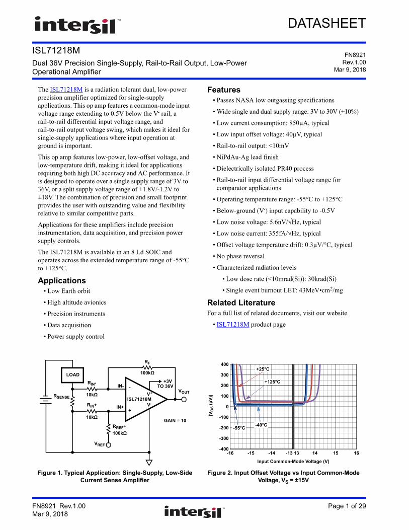
Figure 1. Typical Application: Single-Supply, Low-Side Current Sense Amplifier
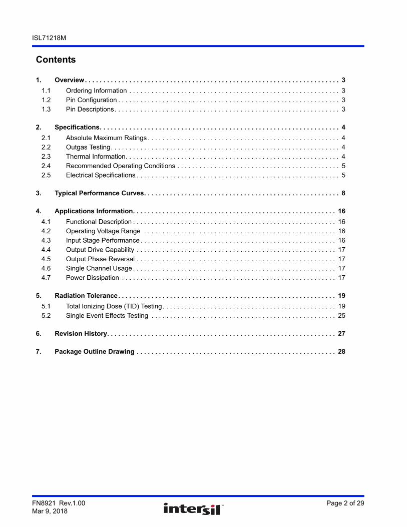
Figure 2. Input Offset Voltage vs Input Common-Mode Voltage, VS = ±15V
IN-
IN+
RF
RREF+
ISL71218M
+3V
V-
V+
RIN-
10kΩ
RIN+
10kΩ
-
+
100kΩ
VREF
100kΩ
VOUT
LOAD
RSENSE
GAIN = 10
TO 36V
|VO
S (
µV
)|
Input Common-Mode Voltage (V)
-400
-300
-200
-100
0
100
200
300
400
-16 -15 -14 -13 13 14 15 16
+125°C
-40°C
+25°C
-55°C
FN8921 Rev.1.00 Page 1 of 29Mar 9, 2018
ISL71218M
Contents
1. Overview. . . . . . . . . . . . . . . . . . . . . . . . . . . . . . . . . . . . . . . . . . . . . . . . . . . . . . . . . . . . . . . . . . . . . 3
1.1 Ordering Information . . . . . . . . . . . . . . . . . . . . . . . . . . . . . . . . . . . . . . . . . . . . . . . . . . . . . . . . . 3
1.2 Pin Configuration . . . . . . . . . . . . . . . . . . . . . . . . . . . . . . . . . . . . . . . . . . . . . . . . . . . . . . . . . . . . 3
1.3 Pin Descriptions. . . . . . . . . . . . . . . . . . . . . . . . . . . . . . . . . . . . . . . . . . . . . . . . . . . . . . . . . . . . . 3
2. Specifications. . . . . . . . . . . . . . . . . . . . . . . . . . . . . . . . . . . . . . . . . . . . . . . . . . . . . . . . . . . . . . . . . 4
2.1 Absolute Maximum Ratings . . . . . . . . . . . . . . . . . . . . . . . . . . . . . . . . . . . . . . . . . . . . . . . . . . . . 4
2.2 Outgas Testing. . . . . . . . . . . . . . . . . . . . . . . . . . . . . . . . . . . . . . . . . . . . . . . . . . . . . . . . . . . . . . 4
2.3 Thermal Information. . . . . . . . . . . . . . . . . . . . . . . . . . . . . . . . . . . . . . . . . . . . . . . . . . . . . . . . . . 4
2.4 Recommended Operating Conditions . . . . . . . . . . . . . . . . . . . . . . . . . . . . . . . . . . . . . . . . . . . . 5
2.5 Electrical Specifications . . . . . . . . . . . . . . . . . . . . . . . . . . . . . . . . . . . . . . . . . . . . . . . . . . . . . . . 5
3. Typical Performance Curves. . . . . . . . . . . . . . . . . . . . . . . . . . . . . . . . . . . . . . . . . . . . . . . . . . . . . 8
4. Applications Information. . . . . . . . . . . . . . . . . . . . . . . . . . . . . . . . . . . . . . . . . . . . . . . . . . . . . . . 16
4.1 Functional Description . . . . . . . . . . . . . . . . . . . . . . . . . . . . . . . . . . . . . . . . . . . . . . . . . . . . . . . 16
4.2 Operating Voltage Range . . . . . . . . . . . . . . . . . . . . . . . . . . . . . . . . . . . . . . . . . . . . . . . . . . . . 16
4.3 Input Stage Performance . . . . . . . . . . . . . . . . . . . . . . . . . . . . . . . . . . . . . . . . . . . . . . . . . . . . . 16
4.4 Output Drive Capability . . . . . . . . . . . . . . . . . . . . . . . . . . . . . . . . . . . . . . . . . . . . . . . . . . . . . . 17
4.5 Output Phase Reversal . . . . . . . . . . . . . . . . . . . . . . . . . . . . . . . . . . . . . . . . . . . . . . . . . . . . . . 17
4.6 Single Channel Usage . . . . . . . . . . . . . . . . . . . . . . . . . . . . . . . . . . . . . . . . . . . . . . . . . . . . . . . 17
4.7 Power Dissipation . . . . . . . . . . . . . . . . . . . . . . . . . . . . . . . . . . . . . . . . . . . . . . . . . . . . . . . . . . 17
5. Radiation Tolerance. . . . . . . . . . . . . . . . . . . . . . . . . . . . . . . . . . . . . . . . . . . . . . . . . . . . . . . . . . . 19
5.1 Total Ionizing Dose (TID) Testing. . . . . . . . . . . . . . . . . . . . . . . . . . . . . . . . . . . . . . . . . . . . . . . 19
5.2 Single Event Effects Testing . . . . . . . . . . . . . . . . . . . . . . . . . . . . . . . . . . . . . . . . . . . . . . . . . . 25
6. Revision History. . . . . . . . . . . . . . . . . . . . . . . . . . . . . . . . . . . . . . . . . . . . . . . . . . . . . . . . . . . . . . 27
7. Package Outline Drawing . . . . . . . . . . . . . . . . . . . . . . . . . . . . . . . . . . . . . . . . . . . . . . . . . . . . . . 28
FN8921 Rev.1.00 Page 2 of 29Mar 9, 2018
ISL71218M
1. Overview
1.1 Ordering Information
1.2 Pin ConfigurationISL71218M(8 Ld SOIC)
Top View
1.3 Pin Descriptions
Part Number (Notes 2, 3)
PartMarking
Temp Range(°C)
Tape and Reel(Units)
Package(RoHS Compliant)
Pkg. Dwg. #
ISL71218MBZ 71218 MBZ -55 to +125 - 8 Ld SOIC M8.15
ISL71218MBZ-T (Note 1) 71218 MBZ -55 to +125 1k 8 Ld SOIC M8.15
ISL71218MBZ-T7A (Note 1) 71218 MBZ -55 to +125 250 8 Ld SOIC M8.15
ISL71218MEVAL1Z Evaluation Board
Notes:1. Refer to TB347 for details about reel specifications. 2. These Pb-free plastic packaged products employ special Pb-free material sets; molding compounds/die attach materials and
NiPdAu-Ag plate - e4 termination finish, which is RoHS compliant and compatible with both SnPb and Pb-free soldering operations. Pb-free products are MSL classified at Pb-free peak reflow temperatures that meet or exceed the Pb-free requirements of IPC/JEDEC J STD-020.
3. For Moisture Sensitivity Level (MSL), refer to the ISL71218M product information page. For more information about MSL, refer to TB363.
Pin Number Pin Name Equivalent Circuit Description
1 OUT_A Circuit 2 Amplifier A output
2 -IN_A Circuit 1 Amplifier A inverting input
3 +IN_A Circuit 1 Amplifier A non-inverting input
4 V- Circuit 1, 2, 3 Negative power supply
5 +IN_B Circuit 1 Amplifier B non-inverting input
6 -IN_B Circuit 1 Amplifier B inverting input
7 OUT_B Circuit 2 Amplifier B output
8 V+ Circuit 1, 2, 3 Positive power supply
OUT_A
-IN_A
+IN_A
V-
1
2
3
4
8
7
6
5
V+
OUT_B
-IN_B
+IN_B
+-
+ -
V+
V-
OUT
Circuit 2Circuit 1
V+
V-
Circuit 3
IN-
V+
V-
IN+Capacitively
Triggered ESD Clamp
FN8921 Rev.1.00 Page 3 of 29Mar 9, 2018

ISL71218M
2. Specifications
2.1 Absolute Maximum Ratings
CAUTION: Do not operate at or near the maximum ratings listed for extended periods of time. Exposure to such conditions may adversely impact product reliability and result in failures not covered by warranty.
2.2 Outgas Testing
2.3 Thermal Information
Parameter Minimum Maximum Unit
Maximum Supply Voltage 42 V
Maximum Supply Voltage (Note 4) 36 V
Maximum Differential Input Current 20 mA
Maximum Differential Input Voltage V- - 0.5 V+ + 0.5 V
Minimum/Maximum Input Voltage V- - 0.5 V+ + 0.5 V
Minimum/Maximum Input Current ±20 mA
Output Short-Circuit Duration (1 output at a time) Indefinite
ESD Rating Value Unit
Human Body Model (Tested per JS-001-2014) 5.5 kV
Machine Model (Tested per JESD22-A115-C) 300 V
Charged Device Model (Tested per JS-002-2014) 2 kV
Latch-Up (Tested per JESD78E; Class 2, Level A) 100 at +125°C mA
Note:4. Tested in a heavy ion environment at LET = 43MeV•cm2/mg at +125°C (TC) for SEB.
Specification(Tested per ASTM E595, 1.5) Value Unit
Total Mass Lost (Note 5) 0.06 %
Collected Volatile Condensible Material (Note 5) <0.01 %
Water Vapor Recovered 0.03 %
Note:5. Outgassing results meet NASA requirements of total mass loss <1% and collected volatile condensible material of <0.1%.
Thermal Resistance (Typical) JA (°C/W) JC (°C/W)
8 Ld SOIC Package (Notes 6, 7) 105 50
Notes:6. JA is measured with the component mounted on a high-effective thermal conductivity test board in free air. See TB379.7. For JC, the “case temp” location is the package top center.
Parameter Minimum Maximum Unit
Storage Temperature Range -65 +150 °C
Pb-Free Reflow Profile Refer to TB493
FN8921 Rev.1.00 Page 4 of 29Mar 9, 2018
ISL71218M
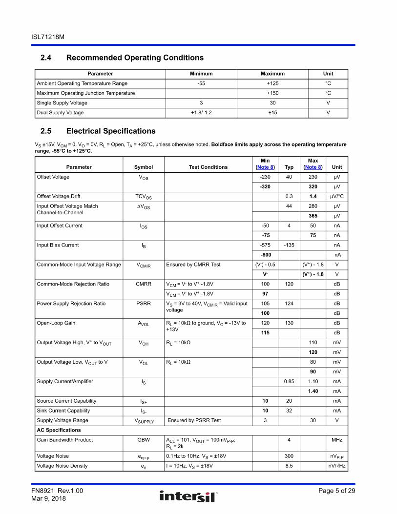
2.4 Recommended Operating Conditions
2.5 Electrical Specifications
Parameter Minimum Maximum Unit
Ambient Operating Temperature Range -55 +125 °C
Maximum Operating Junction Temperature +150 °C
Single Supply Voltage 3 30 V
Dual Supply Voltage +1.8/-1.2 ±15 V
VS ±15V, VCM = 0, VO = 0V, RL = Open, TA = +25°C, unless otherwise noted. Boldface limits apply across the operating temperature range, -55°C to +125°C.
Parameter Symbol Test ConditionsMin
(Note 8) TypMax
(Note 8) Unit
Offset Voltage VOS -230 40 230 µV
-320 320 µV
Offset Voltage Drift TCVOS 0.3 1.4 µV/°C
Input Offset Voltage Match Channel-to-Channel
VOS 44 280 µV
365 µV
Input Offset Current IOS -50 4 50 nA
-75 75 nA
Input Bias Current IB -575 -135 nA
-800 nA
Common-Mode Input Voltage Range VCMIR Ensured by CMRR Test (V-) - 0.5 (V+) - 1.8 V
V- (V+) - 1.8 V
Common-Mode Rejection Ratio CMRR VCM = V- to V+ -1.8V 100 120 dB
VCM = V- to V+ -1.8V 97 dB
Power Supply Rejection Ratio PSRR VS = 3V to 40V, VCMIR = Valid input voltage
105 124 dB
100 dB
Open-Loop Gain AVOL RL = 10kΩ to ground, VO = -13V to +13V
120 130 dB
115 dB
Output Voltage High, V+ to VOUT VOH RL = 10kΩ 110 mV
120 mV
Output Voltage Low, VOUT to V- VOL RL = 10kΩ 80 mV
90 mV
Supply Current/Amplifier IS 0.85 1.10 mA
1.40 mA
Source Current Capability IS+ 10 20 mA
Sink Current Capability IS- 10 32 mA
Supply Voltage Range VSUPPLY Ensured by PSRR Test 3 30 V
AC Specifications
Gain Bandwidth Product GBW ACL = 101, VOUT = 100mVP-P; RL = 2k
4 MHz
Voltage Noise enp-p 0.1Hz to 10Hz, VS = ±18V 300 nVP-P
Voltage Noise Density en f = 10Hz, VS = ±18V 8.5 nV/Hz
FN8921 Rev.1.00 Page 5 of 29Mar 9, 2018
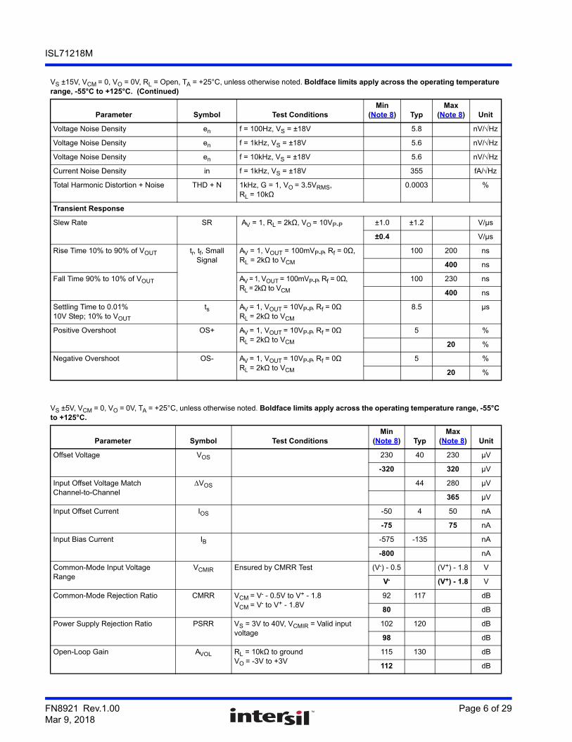
ISL71218M
Voltage Noise Density en f = 100Hz, VS = ±18V 5.8 nV/Hz
Voltage Noise Density en f = 1kHz, VS = ±18V 5.6 nV/Hz
Voltage Noise Density en f = 10kHz, VS = ±18V 5.6 nV/Hz
Current Noise Density in f = 1kHz, VS = ±18V 355 fA/Hz
Total Harmonic Distortion + Noise THD + N 1kHz, G = 1, VO = 3.5VRMS, RL = 10kΩ
0.0003 %
Transient Response
Slew Rate SR AV = 1, RL = 2kΩ, VO = 10VP-P ±1.0 ±1.2 V/µs
±0.4 V/µs
Rise Time 10% to 90% of VOUT tr, tf, Small Signal
AV = 1, VOUT = 100mVP-P, Rf = 0Ω, RL = 2kΩ to VCM
100 200 ns
400 ns
Fall Time 90% to 10% of VOUT AV = 1, VOUT = 100mVP-P, Rf = 0ΩRL = 2kΩto VCM
100 230 ns
400 ns
Settling Time to 0.01%10V Step; 10% to VOUT
ts AV = 1, VOUT = 10VP-P, Rf = 0ΩRL = 2kΩ to VCM
8.5 µs
Positive Overshoot OS+ AV = 1, VOUT = 10VP-P, Rf = 0ΩRL = 2kΩ to VCM
5 %
20 %
Negative Overshoot OS- AV = 1, VOUT = 10VP-P, Rf = 0ΩRL = 2kΩ to VCM
5 %
20 %
VS ±5V, VCM = 0, VO = 0V, TA = +25°C, unless otherwise noted. Boldface limits apply across the operating temperature range, -55°C to +125°C.
Parameter Symbol Test ConditionsMin
(Note 8) TypMax
(Note 8) Unit
Offset Voltage VOS 230 40 230 µV
-320 320 µV
Input Offset Voltage Match Channel-to-Channel
VOS 44 280 µV
365 µV
Input Offset Current IOS -50 4 50 nA
-75 75 nA
Input Bias Current IB -575 -135 nA
-800 nA
Common-Mode Input Voltage Range
VCMIR Ensured by CMRR Test (V-) - 0.5 (V+) - 1.8 V
V- (V+) - 1.8 V
Common-Mode Rejection Ratio CMRR VCM = V- - 0.5V to V+ - 1.8VCM = V- to V+ - 1.8V
92 117 dB
80 dB
Power Supply Rejection Ratio PSRR VS = 3V to 40V, VCMIR = Valid input voltage
102 120 dB
98 dB
Open-Loop Gain AVOL RL = 10kΩ to groundVO = -3V to +3V
115 130 dB
112 dB
VS ±15V, VCM = 0, VO = 0V, RL = Open, TA = +25°C, unless otherwise noted. Boldface limits apply across the operating temperature range, -55°C to +125°C. (Continued)
Parameter Symbol Test ConditionsMin
(Note 8) TypMax
(Note 8) Unit
FN8921 Rev.1.00 Page 6 of 29Mar 9, 2018

ISL71218M
Output Voltage High,V+ to VOUT
VOH RL = 10kΩ 36 65 mV
70 mV
Output Voltage Low,VOUT to V-
VOL RL = 10kΩ 28 45 mV
50 mV
Supply Current/Amplifier IS 0.74 1.10 mA
1.40 mA
Source Current Capability IS+ TA = +25°C, +125°C 10 13 mA
TA = -55°C 6 mA
Sink Current Capability IS- 10 23 mA
AC Specifications
Gain Bandwidth Product GBW 3.2 MHz
Voltage Noise enp-p 0.1Hz to 10Hz 320 nVP-P
Voltage Noise Density en f = 10Hz 9 nV/Hz
Voltage Noise Density en f = 100Hz 5.7 nV/Hz
Voltage Noise Density en f = 1kHz 5.5 nV/Hz
Voltage Noise Density en f = 10kHz 5.5 nV/Hz
Current Noise Density in f = 1kHz 380 fA/Hz
Total Harmonic Distortion + Noise THD + N 1kHz, G = 1, VO = 1.25VRMS, RL = 10kΩ
0.0003 %
Transient Response
Slew Rate SR AV = 1, RL = 2kΩVO = 4VP-P ±1 V/µs
Rise Time 10% to 90% of VOUT tr, tf, Small Signal
AV = 1, VOUT = 100mVP-P , Rf = 0Ω, RL = 2kΩ to VCM
100 ns
Fall Time 90% to 10% of VOUT AV = 1, VOUT = 100mVP-P, Rf = 0Ω, RL = 2kΩ to VCM
100 ns
Settling Time to 0.01%4V Step; 10% to VOUT
ts AV = 1, VOUT = 4VP-P, Rf = 0ΩRL = 2kΩ to VCM
4 µs
Positive Overshoot OS+ AV = 1, VOUT = 10VP-P, Rf = 0ΩRL = 2kΩ to VCM
5 %
Negative Overshoot OS- AV = 1, VOUT = 10VP-P, Rf = 0ΩRL = 2kΩ to VCM
5 %
Note:8. Compliance to datasheet limits is assured by one or more methods: production test, characterization, and/or design.
VS ±5V, VCM = 0, VO = 0V, TA = +25°C, unless otherwise noted. Boldface limits apply across the operating temperature range, -55°C to +125°C. (Continued)
Parameter Symbol Test ConditionsMin
(Note 8) TypMax
(Note 8) Unit
FN8921 Rev.1.00 Page 7 of 29Mar 9, 2018

ISL71218M
3. Typical Performance CurvesVS = ±15V, VCM = 0V, RL = Open, TA = +25°C, unless otherwise specified. (Continued)
Figure 3. VOS vs Temperature Figure 4. Input Offset Voltage vs Input Common-Mode Voltage, VS = ±15V
Figure 5. IBIAS vs VS Figure 6. IBIAS vs Temperature vs Supply
Figure 7. CMRR vs Temperature, VS = ±15V Figure 8. CMRR vs Temperature, VS = ±5V
0
10
20
30
40
50
60
70
80
90
100
-60 -40 -20 0 20 40 60 80 100 120 140 160
VO
S (
µV
)
Temperature (°C)
VS = ±5V
VS = ±15V
|VO
S (
µV
)|
Input Common-Mode Voltage (V)
-400
-300
-200
-100
0
100
200
300
400
-16 -15 -14 -13 13 14 15 16
+125°C
-40°C
+25°C
-55°C
I BIA
S (
nA
)
-500
-450
-400
-350
-300
-250
-200
-150
-100
-50
0
2 4 6 8 10 12 14 16 18 20 22 24 26 28 30 32 34 36 38 40
VS (V)
I BIA
S (
nA
)
-400
-350
-300
-250
-200
-150
Temperature (°C)
-60 -20 0 20 40 60 80 100 120
VS = +40V
-40 140
VS = +3.0V
VS = +4.5VVS = +10V
VS = +30V
Temperature (°C)
CM
RR
(d
B)
110
112
114
116
118
120
122
124
126
128
130
132
-60 -40 -20 0 20 40 60 80 100 120 140 160
Channel-A
Channel-B
Temperature (°C)
CM
RR
(d
B)
110
112
114
116
118
120
122
124
126
128
130
132
-60 -40 -20 0 20 40 60 80 100 120 140 160
Channel-A
Channel-B
FN8921 Rev.1.00 Page 8 of 29Mar 9, 2018

ISL71218M
Figure 9. CMRR vs Frequency, VS = ±15V Figure 10. PSRR vs Temperature, VS = ±15V
Figure 11. PSRR vs Frequency, VS = ±15V Figure 12. PSRR vs Frequency, VS = ±5V
Figure 13. Open-Loop Gain, Phase vs Frequency, VS = ±15V
Figure 14. Frequency Response vs Closed-Loop Gain
CM
RR
(d
B)
Frequency (Hz)
0102030405060708090
100110120130140
1m 1 10 100 1k 10k 100k 1M 10M 100M 1G0.10.01
VS = ±15VSimulation
-60 -40 -20 0 20 40 60 80 100 120 140 160Temperature (°C)
100
105
110
115
120
125
130
135
140
PS
RR
(d
B)
10 100 1k 10k 100k 1M 10M
PS
RR
(d
B)
Frequency (Hz)
-100
102030405060708090
100110120130140
VS = ±15V
CL = 4pF
VCM = 1VP-P
RL = 10k
AV = 1
PSRR-
PSRR+
10 100 1k 10k 100k 1M 10M
PS
RR
(d
B)
Frequency (Hz)
-100
102030405060708090
100110120130140
VS = ±5V
CL = 4pF
VCM = 1VP-P
RL = 10k
AV = 1
PSRR-
PSRR+
-100-80-60-40-20
020406080
100120140160180200
1m 1 10 100 1k 10k 100k 1M 10M 100M 1G
Ga
in (
dB
)
Frequency (Hz)
0.1
VS = ±15VRL = 1MΩ
0.01
Gain
Phase
-10
0
10
20
30
40
50
60
70
1k 10k 100k 1M 10M
Ga
in (
dB
)
Frequency (Hz)
ACL = 1
ACL = 10
ACL = 100
ACL = 1000
100
VS = ±5V and ±15VCL = 4pF, RL = 2kVOUT = 100mVP-P
RF = 10kΩ, RG = 100Ω
RF = 10kΩ, RG = 1kΩ
RF = 0, RG = ∞
RF = 10kΩ, RG = 10Ω
FN8921 Rev.1.00 Page 9 of 29Mar 9, 2018
ISL71218M
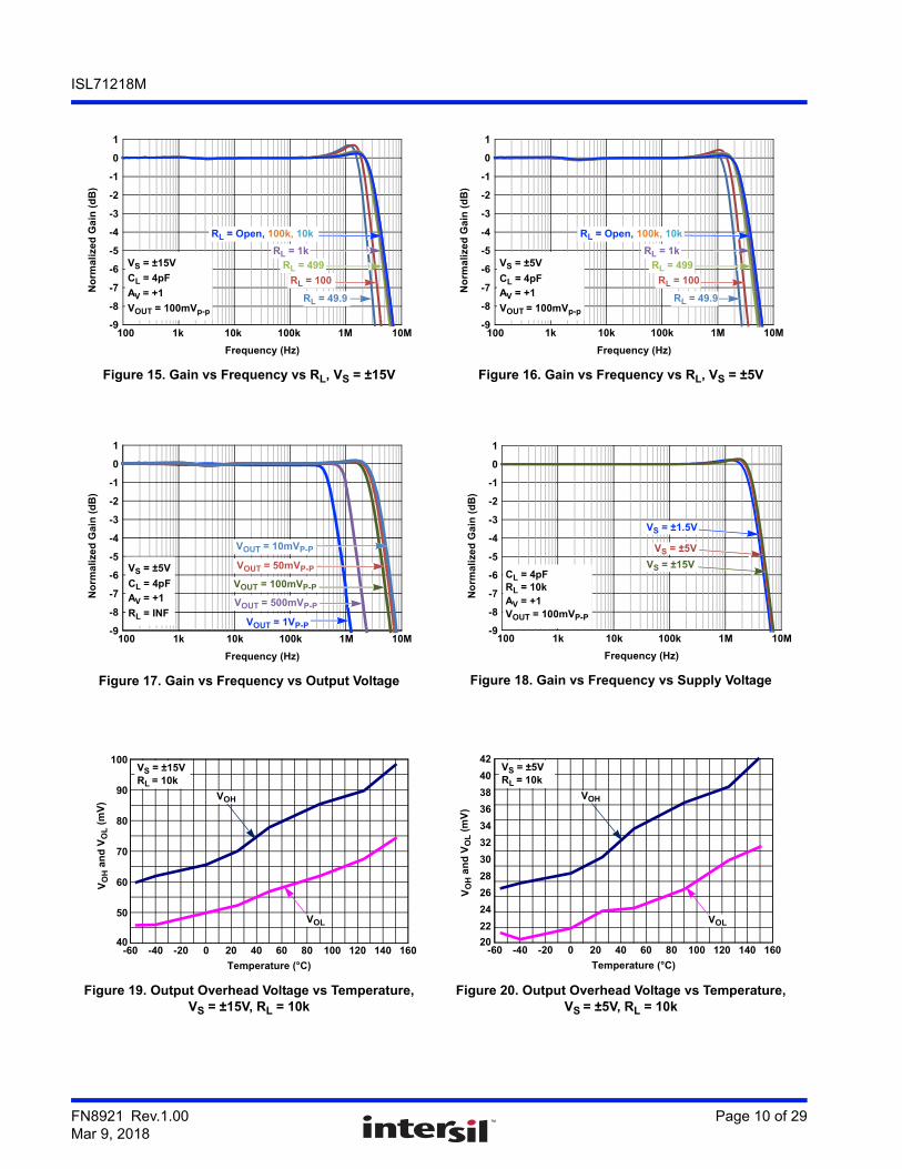
Figure 15. Gain vs Frequency vs RL, VS = ±15V Figure 16. Gain vs Frequency vs RL, VS = ±5V
Figure 17. Gain vs Frequency vs Output Voltage Figure 18. Gain vs Frequency vs Supply Voltage
Figure 19. Output Overhead Voltage vs Temperature, VS = ±15V, RL = 10k
Figure 20. Output Overhead Voltage vs Temperature, VS = ±5V, RL = 10k
Frequency (Hz)
No
rmal
ized
Gai
n (
dB
)
100k 1M 10M10k1k-9
-8
-7
-6
-5
-4
-3
-2
-1
0
1
100
VS = ±15V
AV = +1
VOUT = 100mVp-p
CL = 4pF
RL = 1k
RL = 499
RL = 100
RL = 49.9
RL = Open, 100k, 10k
Frequency (Hz)
100k 1M 10M10k1k-9
-8
-7
-6
-5
-4
-3
-2
-1
0
1
100
VS = ±5V
AV = +1
VOUT = 100mVp-p
CL = 4pF
RL = Open, 100k, 10k
RL = 1k
RL = 499
RL = 100
RL = 49.9
No
rma
lize
d G
ain
(d
B)
Frequency (Hz)
No
rma
lize
d G
ain
(d
B)
100k 1M 10M10k1k-9
-8
-7
-6
-5
-4
-3
-2
-1
0
1
100
VOUT = 1VP-P
VOUT = 500mVP-P
VOUT = 10mVP-P
VOUT = 50mVP-P
VOUT = 100mVP-P
VS = ±5V
AV = +1
RL = INF
CL = 4pF
No
rma
lize
d G
ain
(d
B)
Frequency (Hz)
-9
-8
-7
-6
-5
-4
-3
-2
-1
0
1
100 1k 10k 100k 1M 10M
CL = 4pFRL = 10kAV = +1VOUT = 100mVP-P
VS = ±15V
VS = ±1.5V
VS = ±5V
40
50
60
70
80
90
100
-60 -40 -20 0 20 40 60 80 100 120 140 160
VO
H a
nd
VO
L (
mV
)
Temperature (°C)
VOH
VS = ±15VRL = 10k
VOL
-60 -40 -20 0 20 40 60 80 100 120 140 160
VO
H a
nd
VO
L (
mV
)
Temperature (°C)
VOH
VS = ±5VRL = 10k
VOL
20
22
24
26
28
30
32
34
36
38
40
42
FN8921 Rev.1.00 Page 10 of 29Mar 9, 2018
ISL71218M
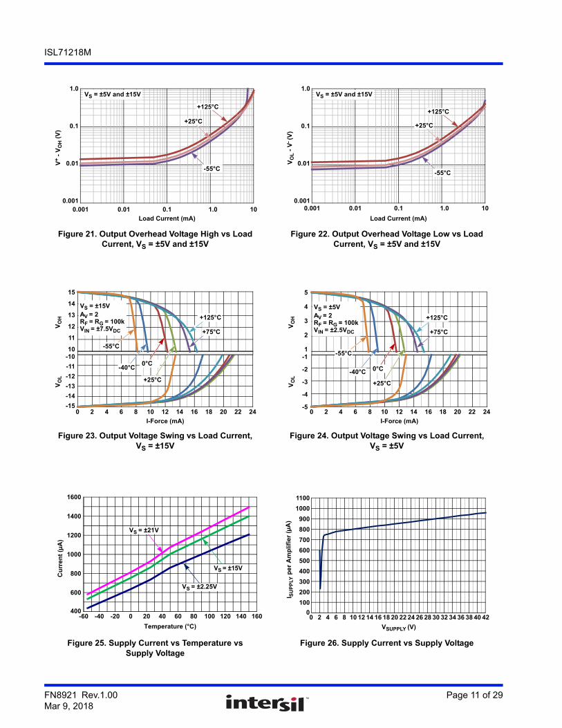
Figure 21. Output Overhead Voltage High vs Load Current, VS = ±5V and ±15V
Figure 22. Output Overhead Voltage Low vs Load Current, VS = ±5V and ±15V
Figure 23. Output Voltage Swing vs Load Current, VS = ±15V
Figure 24. Output Voltage Swing vs Load Current, VS = ±5V
Figure 25. Supply Current vs Temperature vs Supply Voltage
Figure 26. Supply Current vs Supply Voltage
V+ -
VO
H (
V)
Load Current (mA)
0.001
0.01
0.1
1.0
0.001 0.01 0.1 1.0 10
VS = ±5V and ±15V
+125°C
+25°C
-55°C
Load Current (mA)
0.001
0.01
0.1
1.0
0.001 0.01 0.1 1.0 10
VS = ±5V and ±15V
VO
L -
V- (V
)
+125°C
+25°C
-55°C
VO
H
0
VO
L
I-Force (mA)
11
12
13
14
15
-15
-14
-13
-12
-11
2218161412108642
10-10
0°C-40°C
+25°C
+75°C
+125°C
20 24
-55°C
VS = ±15VAV = 2
VIN = ±7.5VDC
RF = RG = 100k
VO
HV
OL
I-Force (mA)
1
2
3
4
5
-5
-4
-3
-2
-1
VS = ±5VAV = 2
VIN = ±2.5VDC
RF = RG = 100k
0°C-40°C
+25°C
+75°C
+125°C
-55°C
0 2218161412108642 20 24
Temperature (°C)
Cu
rre
nt
(µA
)
400
600
800
1000
1200
1400
1600
-60 -40 -20 0 20 40 60 80 100 120 140 160
VS = ±2.25V
VS = ±15V
VS = ±21V
VSUPPLY (V)
0 2 4 6 8 10 12 14 16 18 20 22 24 26 28 30 32 34 36 38 40 420
100
200
300
400
500
600
700
800
900
1000
1100
I SU
PP
LY p
er
Am
pli
fie
r (µ
A)
FN8921 Rev.1.00 Page 11 of 29Mar 9, 2018
ISL71218M
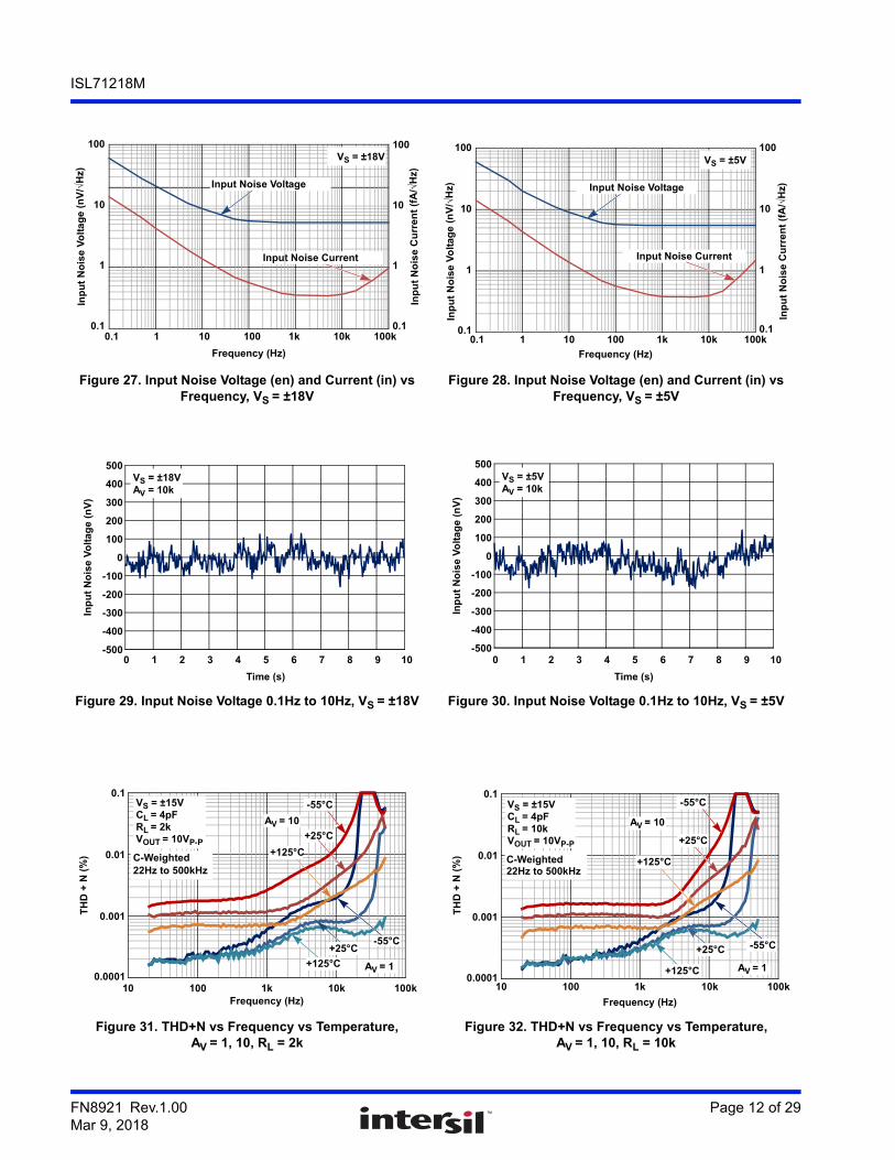
Figure 27. Input Noise Voltage (en) and Current (in) vs Frequency, VS = ±18V
Figure 28. Input Noise Voltage (en) and Current (in) vs Frequency, VS = ±5V
Figure 29. Input Noise Voltage 0.1Hz to 10Hz, VS = ±18V Figure 30. Input Noise Voltage 0.1Hz to 10Hz, VS = ±5V
Figure 31. THD+N vs Frequency vs Temperature,AV = 1, 10, RL = 2k
Figure 32. THD+N vs Frequency vs Temperature,AV = 1, 10, RL = 10k
0.1
1
10
100
0.1
1
10
100
0.1 1 10 100 1k 10k 100k
Inp
ut
No
ise
Vo
lta
ge
(n
V/√
Hz)
Frequency (Hz)
Inp
ut
No
ise
Cu
rre
nt
(fA
/√H
z)
VS = ±18V
Input Noise Voltage
Input Noise Current
0.1
1
10
100
0.1
1
10
100
0.1 1 10 100 1k 10k 100k
Inp
ut
No
ise
Vo
ltag
e (
nV
/√H
z)
Frequency (Hz)
Inp
ut
No
ise
Cu
rre
nt
(fA
/√H
z)
Input Noise Current
VS = ±5V
Input Noise Voltage
Inp
ut
No
ise
Vo
ltag
e (n
V)
0 1 2 3 4 5 6 7 8 9 10
Time (s)
-500
-400
-300
-200
-100
0
100
200
300
400
500VS = ±18VAV = 10k
Inp
ut
No
ise
Vo
ltag
e (n
V)
0 1 2 3 4 5 6 7 8 9 10
Time (s)
-500
-400
-300
-200
-100
0
100
200
300
400
500VS = ±5VAV = 10k
0.0001
0.001
0.01
0.1
10 100 1k 10k 100k
TH
D +
N (
%)
Frequency (Hz)
AV = 1
AV = 10
VS = ±15VCL = 4pF
VOUT = 10VP-P
RL = 2k
C-Weighted22Hz to 500kHz
+25°C
-55°C+25°C
+125°C
-55°C
+125°C
0.0001
0.001
0.01
0.1
10 100 1k 10k 100k
TH
D +
N (
%)
Frequency (Hz)
AV = 10
VS = ±15VCL = 4pF
VOUT = 10VP-P
RL = 10k
C-Weighted22Hz to 500kHz
+125°C
+25°C
-55°C
AV = 1
-55°C+25°C
+125°C
FN8921 Rev.1.00 Page 12 of 29Mar 9, 2018
ISL71218M
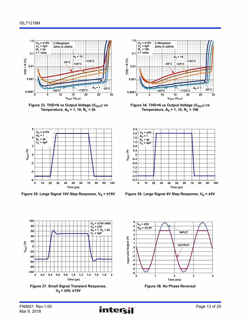
Figure 33. THD+N vs Output Voltage (VOUT) vs Temperature, AV = 1, 10, RL = 2k
Figure 34. THD+N vs Output Voltage (VOUT) vs Temperature, AV = 1, 10, RL = 10k
Figure 35. Large Signal 10V Step Response, VS = ±15V Figure 36. Large Signal 4V Step Response, VS = ±5V
Figure 37. Small Signal Transient Response,VS = ±5V, ±15V
Figure 38. No Phase Reversal
0.0001
0.001
0.01
0.1
1.0
0 5 10 15 20 25 30VOUT (VP-P)
TH
D +
N (
%)
AV = 1
C-Weighted22Hz to 22kHz
AV = 10
-55°C
VS = ±15VCL = 4pF
f = 1kHzRL = 2k
-55°C+125°C+25°C
+125°C+25°C
0.0001
0.001
0.01
0.1
1.0
0 5 10 15 20 25 30VOUT (VP-P)
TH
D +
N (
%)
AV = 1
AV = 10
C-Weighted22Hz to 22kHz
VS = ±15VCL = 4pF
f = 1kHzRL = 10k
+125°C+25°C -55°C
+25°C-55°C+125°C
-6
-4
-2
0
2
4
6
0 10 20 30 40 50 60 70 80 90 100
VO
UT (
V)
Time (µs)
VS = ±15VAV = 1RL = 2kCL = 4pF
0 10 20 30 40 50 60 70 80 90 100
VO
UT (
V)
Time (µs)
-2.4-2.0
-1.6
-1.2
-0.8
-0.4
0
0.4
0.8
1.2
1.6
2.0
2.4VS = ±5VAV = 1RL = 2kCL = 4pF
VO
UT (
V)
Time (µs)
-100
-80
-60
-40
-20
0
20
40
60
80
100
0 0.2 0.4 0.6 0.8 1.0 1.2 1.4 1.6 1.8 2
VS = ±15V AND
AV = 1, RL = 2kCL = 4pF
VS = ±5V
-6
-5
-4
-3
-2
-1
0
1
2
3
4
5
6
0 1 2 3 4
Inp
ut
an
d O
utp
ut
(V)
Time (ms)
VS = ±5VVIN = ±5.9V
INPUT
OUTPUT
FN8921 Rev.1.00 Page 13 of 29Mar 9, 2018

ISL71218M
Figure 39. Positive Output Overload Response Time,VS = ±15V
Figure 40. Negative Output Overload Response Time,VS = ±15V
Figure 41. Positive Output Overload Response Time,VS = ±5V
Figure 42. Negative Output Overload Response Time,VS = ±5V
Figure 43. Output Impedance vs Frequency, VS = ±15V Figure 44. Output Impedance vs Frequency, VS = ±5V
Ou
tpu
t (V
)
Inp
ut
(mV
)
Time (µs)
0
4
8
12
16
20
0
40
80
120
160
200
0 4 8 12 16 20 24 28 32 36 40
VS = ±15VAV = 100
VIN = 100mVP-POverdrive = 1V
RL = 10k
Output
Input
Ou
tpu
t (V
)
Inp
ut
(mV
)
Time (µs)
-20
-16
-12
-8
-4
0
-200
-160
-120
-80
-40
0
0 4 8 12 16 20 24 28 32 36 40
VS = ±15VAV = 100
VIN = 100mVP-POverdrive = 1V
RL = 10k
Output
Input
Ou
tpu
t (V
)
Inp
ut
(mV
)
Time (µs)
0
1
2
3
4
5
6
0
10
20
30
40
50
60
0 4 8 12 16 20 24 28 32 36 40
VS = ±5VAV = 100
VIN = 50mVP-POverdrive = 1V
RL = 10kInput
Output
Ou
tpu
t (V
)
Inp
ut
(mV
)
Time (µs)
0 4 8 12 16 20 24 28 32 36 40-6
-5
-4
-3
-2
-1
0
-60
-50
-40
-30
-20
-10
0
VS = ±5VAV = 100
VIN = 50mVP-POverdrive = 1V
RL = 10k
Output
Input
0.01
0.10
1
10
100
10 100 1k 10k 100k 1M 10M
ZO
UT (
Ω)
Frequency (Hz)
1
VS = ±15V
AV = 1
AV = 10
AV = 100
0.01
0.10
1
10
100
10 100 1k 10k 100k 1M 10M
ZO
UT (
Ω)
Frequency (Hz)
1
VS = ±5V
AV = 1
AV = 10
AV = 100
FN8921 Rev.1.00 Page 14 of 29Mar 9, 2018
ISL71218M
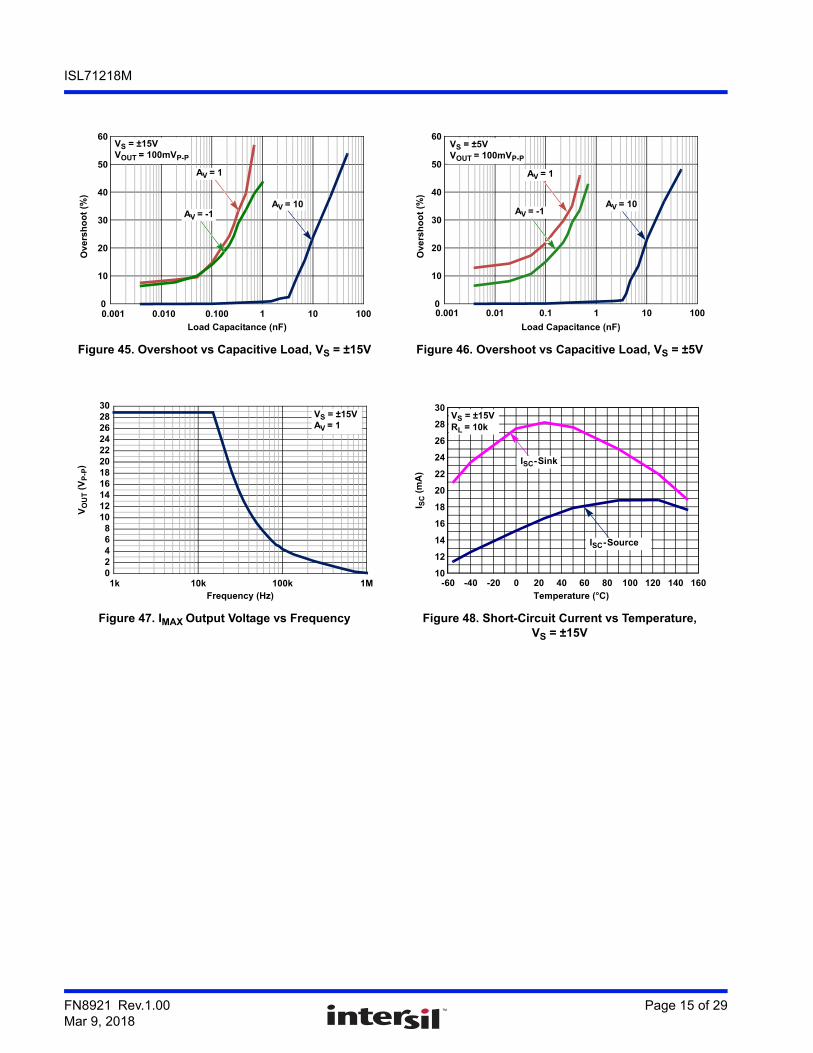
Figure 45. Overshoot vs Capacitive Load, VS = ±15V Figure 46. Overshoot vs Capacitive Load, VS = ±5V
Figure 47. IMAX Output Voltage vs Frequency Figure 48. Short-Circuit Current vs Temperature, VS = ±15V
Ov
ers
ho
ot
(%)
Load Capacitance (nF)
0
10
20
30
40
50
60
0.001 0.010 0.100 1 10 100
VS = ±15VVOUT = 100mVP-P
AV = 10
AV = 1
AV = -1
Ove
rsh
oo
t (%
)
Load Capacitance (nF)
0
10
20
30
40
50
60
0.001 0.01 0.1 1 10 100
VS = ±5VVOUT = 100mVP-P
AV = 10
AV = 1
AV = -1
02468
1012141618202224262830
1k 10k 100k 1M
VO
UT (
VP
-P)
Frequency (Hz)
VS = ±15VAV = 1
-60 -40 -20 0 20 40 60 80 100 120 140 160Temperature (°C)
10
12
14
16
18
20
22
24
26
28
30I S
C (
mA
)
ISC-Source
VS = ±15VRL = 10k
ISC-Sink
FN8921 Rev.1.00 Page 15 of 29Mar 9, 2018
ISL71218M
4. Applications Information
4.1 Functional DescriptionThe ISL71218M is a dual, 3.2MHz, single or dual supply, rail-to-rail output amplifier with a common-mode input voltage range extending to a range of 0.5V below the V- rail. The input stage is optimized for precision sensing of ground-referenced signals in single-supply applications. The input stage is able to handle large input differential voltages without phase inversion, making this amplifier suitable for high-voltage comparator applications. The bipolar design features high open-loop gain and excellent DC input and output temperature stability. This op amp features very low quiescent current of 850µA, and low temperature drift. The device is fabricated in a new precision 40V complementary bipolar DI process and is immune from latch-up for up to a 36V supply range.
4.2 Operating Voltage RangeThe op amp is designed to operate over a single supply range of 3V to 36V, or a split supply voltage range of +1.8V/-1.2V to ±18V. The device is fully characterized at 30V (±15V). Both DC and AC performance remain virtually unchanged over the complete operating voltage range. Parameter variation with operating voltage is shown in the “Typical Performance Curves” on page 8.
The input common-mode voltage to the V+ rail (V+ - 1.8V across the full temperature range) may limit amplifier operation when operating from split V+ and V- supplies. Figure 4 on page 8 shows the common-mode input voltage range variation over temperature.
4.3 Input Stage Performance The ISL71218M PNP input stage has a common-mode input range extending up to 0.5V below ground at +25°C. Full amplifier performance is ensured for input voltage down to ground (V-) across the -55°C to +125°C temperature range. For common-mode voltages down to -0.5V below ground (V-), the amplifiers are fully functional, but performance degrades slightly over the full temperature range. This feature provides excellent CMRR, AC performance, and DC accuracy when amplifying low-level, ground-referenced signals. The input stage has a maximum input differential voltage equal to a diode drop greater than the supply voltage and does not contain the back-to-back input protection diodes found on many similar amplifiers. This feature enables the device to function as a precision comparator by maintaining very high input impedance for high-voltage differential input comparator voltages. The high differential input impedance also enables the device to operate reliably in large signal pulse applications, without the need for anti-parallel clamp diodes required on MOSFET and most bipolar input stage op amps. Thus, input signal distortion caused by nonlinear clamps under high slew rate conditions is avoided.
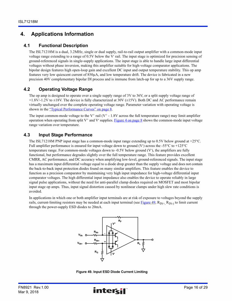
In applications in which one or both amplifier input terminals are at risk of exposure to voltages beyond the supply rails, current-limiting resistors may be needed at each input terminal (see Figure 49, RIN+, RIN-) to limit current through the power-supply ESD diodes to 20mA.
Figure 49. Input ESD Diode Current Limiting
-
+
RIN-
RL
VIN-
V+
V-
RIN+VIN+
RF
RG
FN8921 Rev.1.00 Page 16 of 29Mar 9, 2018
ISL71218M
4.4 Output Drive CapabilityThe bipolar rail-to-rail output stage features low saturation levels that enable an output voltage swing to less than 15mV when the total output load (including feedback resistance) is held below 50µA (Figures 21 and 22). With ±15V supplies, this can be achieved by using feedback resistor values >300kΩ.
The output stage is internally current limited. Output current limit over temperature is shown in Figures 23 and 24 on page 11. The amplifiers can withstand a short-circuit to either rail as long as the power dissipation limits are not exceeded. This applies to only one amplifier at a time for the dual op amp. Continuous operation under these conditions may degrade long-term reliability.
The amplifiers perform well when driving capacitive loads (Figures 45 and 46 on page 15). The unity gain, voltage follower (buffer) configuration provides the highest bandwidth, but is also the most sensitive to ringing produced by load capacitance found in BNC cables. Unity gain overshoot is limited to 35% at capacitance values to 0.33nF. At gains of 10 and higher, the device is capable of driving more than 10nF without significant overshoot.
4.5 Output Phase Reversal Output phase reversal is a change of polarity in the amplifier transfer function when the input voltage exceeds the supply voltage. The ISL71218M is immune to output phase reversal out to 0.5V beyond the rail (VABS MAX) limit (see Figure 38 on page 13).
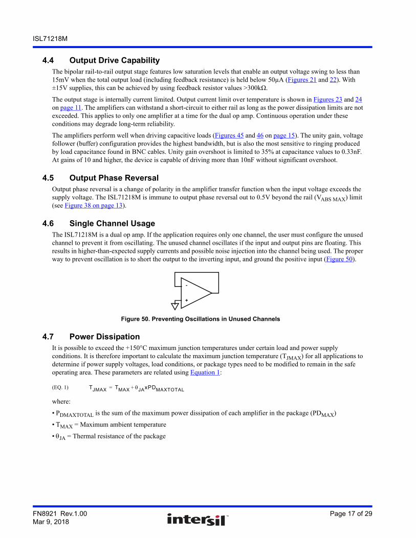
4.6 Single Channel UsageThe ISL71218M is a dual op amp. If the application requires only one channel, the user must configure the unused channel to prevent it from oscillating. The unused channel oscillates if the input and output pins are floating. This results in higher-than-expected supply currents and possible noise injection into the channel being used. The proper way to prevent oscillation is to short the output to the inverting input, and ground the positive input (Figure 50).
Figure 50. Preventing Oscillations in Unused Channels
4.7 Power DissipationIt is possible to exceed the +150°C maximum junction temperatures under certain load and power supply conditions. It is therefore important to calculate the maximum junction temperature (TJMAX) for all applications to determine if power supply voltages, load conditions, or package types need to be modified to remain in the safe operating area. These parameters are related using Equation 1:
where:
• PDMAXTOTAL is the sum of the maximum power dissipation of each amplifier in the package (PDMAX)
• TMAX = Maximum ambient temperature
• JA = Thermal resistance of the package
-
+
TJMAX TMAX JAxPDMAXTOTAL+=(EQ. 1)
FN8921 Rev.1.00 Page 17 of 29Mar 9, 2018

ISL71218M
PDMAX for each amplifier can be calculated using Equation 2:
where:
• PDMAX = Maximum power dissipation of one amplifier
• VS = Total supply voltage
• IqMAX = Maximum quiescent supply current of one amplifier
• VOUTMAX = Maximum output voltage swing of the application
• RL = Load resistance
PDMAX VS IqMAX VS - VOUTMAX VOUTMAX
RL----------------------------+=(EQ. 2)
FN8921 Rev.1.00 Page 18 of 29Mar 9, 2018
ISL71218M
5. Radiation ToleranceThe ISL71218M is a radiation tolerant device for commercial space applications, Low Earth Orbits (LEO) applications, high altitude avionics, launch vehicles, and other harsh environments. This device’s response to Total Ionizing Dose (TID) radiation effects, and Single Event Effects (SEE) has been measured, characterized, and reported in the proceeding sections. However, TID performance is not guaranteed through radiation acceptance testing, nor is the characterized SEE characterized performance guaranteed.
5.1 Total Ionizing Dose (TID) Testing
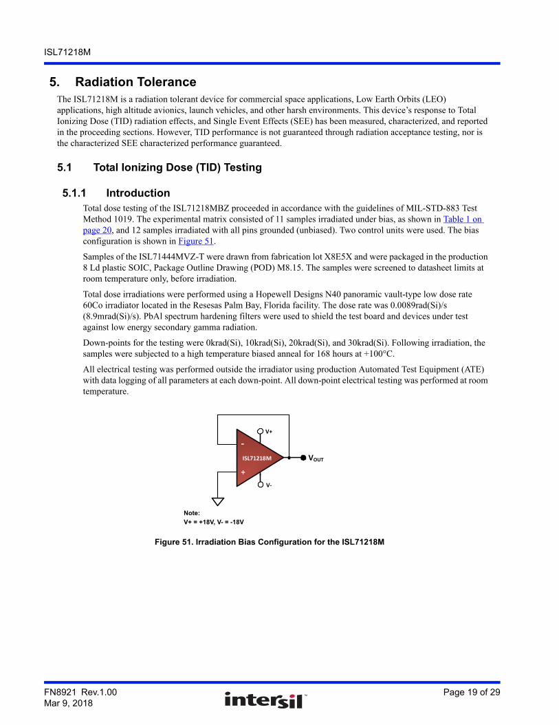
5.1.1 IntroductionTotal dose testing of the ISL71218MBZ proceeded in accordance with the guidelines of MIL-STD-883 Test Method 1019. The experimental matrix consisted of 11 samples irradiated under bias, as shown in Table 1 on page 20, and 12 samples irradiated with all pins grounded (unbiased). Two control units were used. The bias configuration is shown in Figure 51.
Samples of the ISL71444MVZ-T were drawn from fabrication lot X8E5X and were packaged in the production 8 Ld plastic SOIC, Package Outline Drawing (POD) M8.15. The samples were screened to datasheet limits at room temperature only, before irradiation.
Total dose irradiations were performed using a Hopewell Designs N40 panoramic vault-type low dose rate 60Co irradiator located in the Resesas Palm Bay, Florida facility. The dose rate was 0.0089rad(Si)/s (8.9mrad(Si)/s). PbAl spectrum hardening filters were used to shield the test board and devices under test against low energy secondary gamma radiation.
Down-points for the testing were 0krad(Si), 10krad(Si), 20krad(Si), and 30krad(Si). Following irradiation, the samples were subjected to a high temperature biased anneal for 168 hours at +100°C.
All electrical testing was performed outside the irradiator using production Automated Test Equipment (ATE) with data logging of all parameters at each down-point. All down-point electrical testing was performed at room temperature.
Figure 51. Irradiation Bias Configuration for the ISL71218M
Note:
V+ = +18V, V- = -18V
VOUT
+
‐
ISL71218M
V+
V‐
FN8921 Rev.1.00 Page 19 of 29Mar 9, 2018
ISL71218M
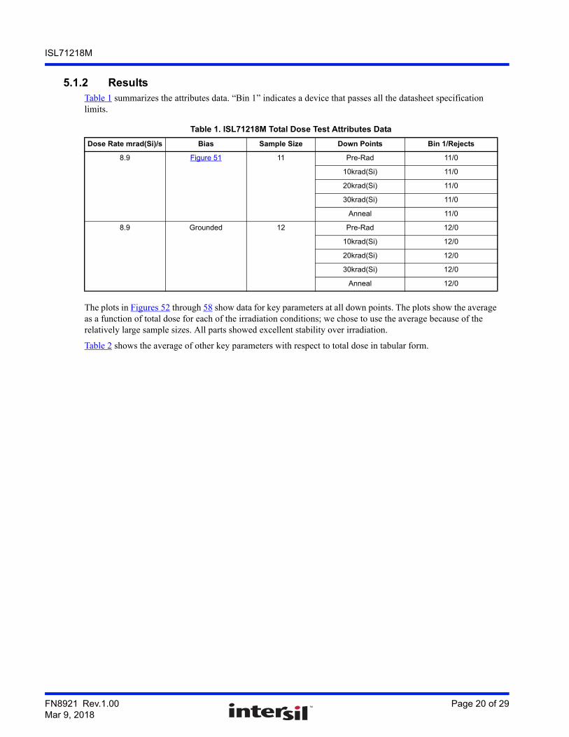
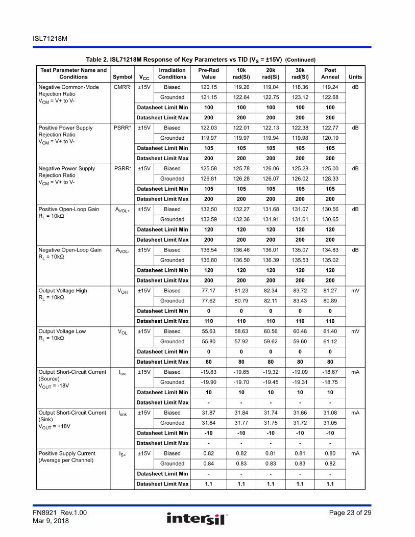
5.1.2 Results Table 1 summarizes the attributes data. “Bin 1” indicates a device that passes all the datasheet specification limits.
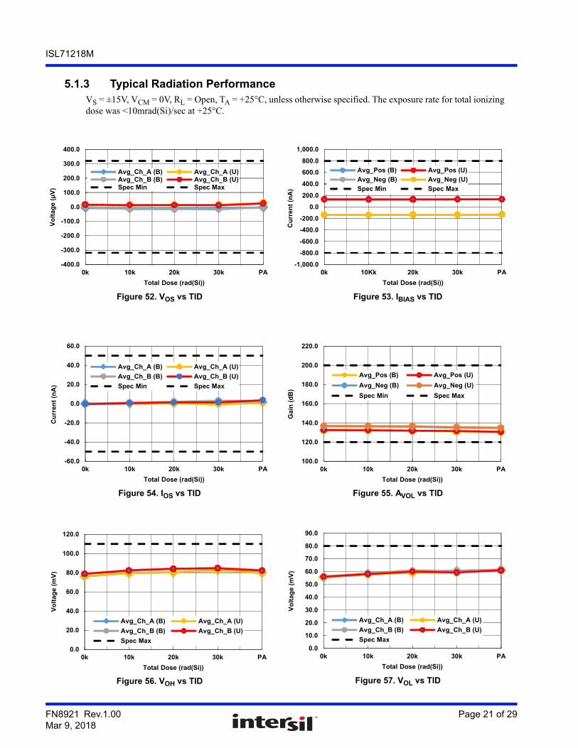
The plots in Figures 52 through 58 show data for key parameters at all down points. The plots show the average as a function of total dose for each of the irradiation conditions; we chose to use the average because of the relatively large sample sizes. All parts showed excellent stability over irradiation.
Table 2 shows the average of other key parameters with respect to total dose in tabular form.
Table 1. ISL71218M Total Dose Test Attributes Data
Dose Rate mrad(Si)/s Bias Sample Size Down Points Bin 1/Rejects
8.9 Figure 51 11 Pre-Rad 11/0
10krad(Si) 11/0
20krad(Si) 11/0
30krad(Si) 11/0
Anneal 11/0
8.9 Grounded 12 Pre-Rad 12/0
10krad(Si) 12/0
20krad(Si) 12/0
30krad(Si) 12/0
Anneal 12/0
FN8921 Rev.1.00 Page 20 of 29Mar 9, 2018
ISL71218M
5.1.3 Typical Radiation PerformanceVS = ±15V, VCM = 0V, RL = Open, TA = +25°C, unless otherwise specified. The exposure rate for total ionizing dose was <10mrad(Si)/sec at +25°C.
Figure 52. VOS vs TID Figure 53. IBIAS vs TID
Figure 54. IOS vs TID Figure 55. AVOL vs TID
Figure 56. VOH vs TID Figure 57. VOL vs TID
-400.0
-300.0
-200.0
-100.0
0.0
100.0
200.0
300.0
400.0
0k 10k 20k 30k PA
Total Dose (rad(Si))
Avg_Ch_A (B) Avg_Ch_A (U)Avg_Ch_B (B) Avg_Ch_B (U)Spec Min Spec Max
Vo
lta
ge
(µ
V)
-1,000.0
-800.0
-600.0
-400.0
-200.0
0.0
200.0
400.0
600.0
800.0
1,000.0
0k 10Kk 20k 30k PA
Total Dose (rad(Si))
Avg_Pos (B) Avg_Pos (U)
Avg_Neg (B) Avg_Neg (U)
Spec Min Spec Max
Cu
rren
t (n
A)
-60.0
-40.0
-20.0
0.0
20.0
40.0
60.0
0k 10k 20k 30k PA
Total Dose (rad(Si))
Avg_Ch_A (B) Avg_Ch_A (U)
Avg_Ch_B (B) Avg_Ch_B (U)
Spec Min Spec Max
Cu
rren
t (n
A)
100.0
120.0
140.0
160.0
180.0
200.0
220.0
0k 10k 20k 30k PA
Total Dose (rad(Si))
Avg_Pos (B) Avg_Pos (U)
Avg_Neg (B) Avg_Neg (U)
Spec Min Spec Max
Ga
in (
dB
)
0.0
20.0
40.0
60.0
80.0
100.0
120.0
0k 10k 20k 30k PA
Total Dose (rad(Si))
Avg_Ch_A (B) Avg_Ch_A (U)
Avg_Ch_B (B) Avg_Ch_B (U)
Spec Max
Vo
ltag
e (m
V)
0.0
10.0
20.0
30.0
40.0
50.0
60.0
70.0
80.0
90.0
0k 10k 20k 30k PA
Total Dose (rad(Si))
Avg_Ch_A (B) Avg_Ch_A (U)
Avg_Ch_B (B) Avg_Ch_B (U)
Spec Max
Vo
lta
ge
(m
V)
FN8921 Rev.1.00 Page 21 of 29Mar 9, 2018
ISL71218M
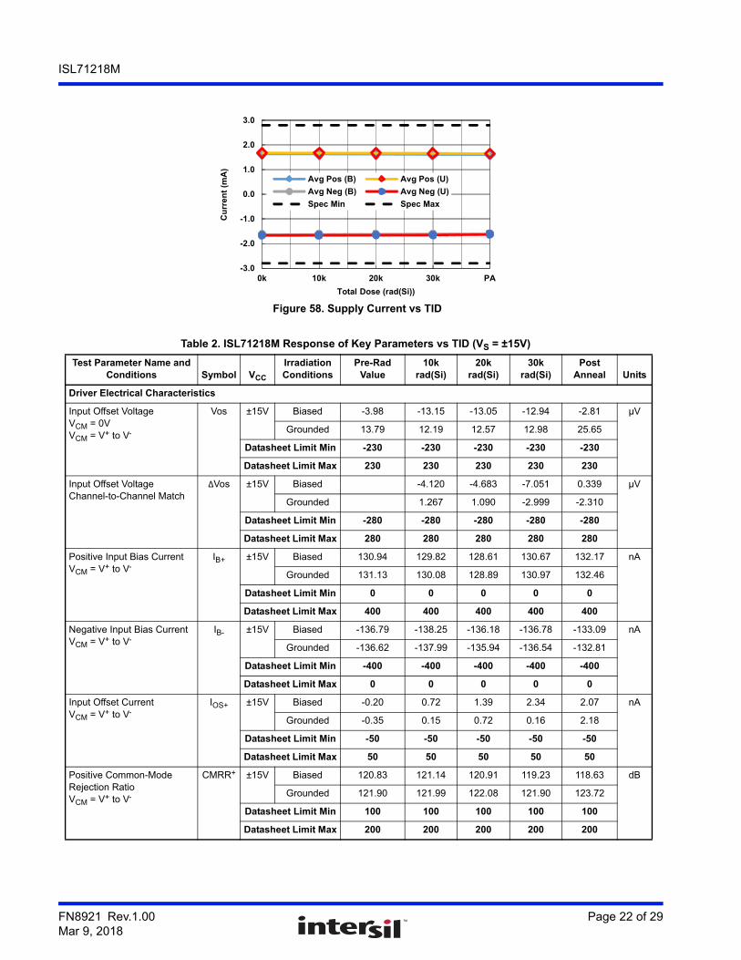
Figure 58. Supply Current vs TID
Table 2. ISL71218M Response of Key Parameters vs TID (VS = ±15V)
Test Parameter Name and Conditions Symbol VCC
Irradiation Conditions
Pre-Rad Value
10k rad(Si)
20k rad(Si)
30k rad(Si)
Post Anneal Units
Driver Electrical Characteristics
Input Offset VoltageVCM = 0VVCM = V+ to V-
Vos ±15V Biased -3.98 -13.15 -13.05 -12.94 -2.81 µV
Grounded 13.79 12.19 12.57 12.98 25.65
Datasheet Limit Min -230 -230 -230 -230 -230
Datasheet Limit Max 230 230 230 230 230
Input Offset Voltage Channel-to-Channel Match
∆Vos ±15V Biased -4.120 -4.683 -7.051 0.339 µV
Grounded 1.267 1.090 -2.999 -2.310
Datasheet Limit Min -280 -280 -280 -280 -280
Datasheet Limit Max 280 280 280 280 280
Positive Input Bias CurrentVCM = V+ to V-
IB+ ±15V Biased 130.94 129.82 128.61 130.67 132.17 nA
Grounded 131.13 130.08 128.89 130.97 132.46
Datasheet Limit Min 0 0 0 0 0
Datasheet Limit Max 400 400 400 400 400
Negative Input Bias CurrentVCM = V+ to V-
IB- ±15V Biased -136.79 -138.25 -136.18 -136.78 -133.09 nA
Grounded -136.62 -137.99 -135.94 -136.54 -132.81
Datasheet Limit Min -400 -400 -400 -400 -400
Datasheet Limit Max 0 0 0 0 0
Input Offset CurrentVCM = V+ to V-
IOS+ ±15V Biased -0.20 0.72 1.39 2.34 2.07 nA
Grounded -0.35 0.15 0.72 0.16 2.18
Datasheet Limit Min -50 -50 -50 -50 -50
Datasheet Limit Max 50 50 50 50 50
Positive Common-Mode Rejection RatioVCM = V+ to V-
CMRR+ ±15V Biased 120.83 121.14 120.91 119.23 118.63 dB
Grounded 121.90 121.99 122.08 121.90 123.72
Datasheet Limit Min 100 100 100 100 100
Datasheet Limit Max 200 200 200 200 200
-3.0
-2.0
-1.0
0.0
1.0
2.0
3.0
0k 10k 20k 30k PA
Total Dose (rad(Si))
Avg Pos (B) Avg Pos (U)
Avg Neg (B) Avg Neg (U)
Spec Min Spec Max
Cu
rre
nt
(mA
)
FN8921 Rev.1.00 Page 22 of 29Mar 9, 2018
ISL71218M
Negative Common-Mode Rejection RatioVCM = V+ to V-
CMRR- ±15V Biased 120.15 119.26 119.04 118.36 119.24 dB
Grounded 121.15 122.64 122.75 123.12 122.68
Datasheet Limit Min 100 100 100 100 100
Datasheet Limit Max 200 200 200 200 200
Positive Power Supply Rejection RatioVCM = V+ to V-
PSRR+ ±15V Biased 122.03 122.01 122.13 122.38 122.77 dB
Grounded 119.97 119.97 119.94 119.98 120.19
Datasheet Limit Min 105 105 105 105 105
Datasheet Limit Max 200 200 200 200 200
Negative Power Supply Rejection RatioVCM = V+ to V-
PSRR- ±15V Biased 125.58 125.78 126.06 125.28 125.00 dB
Grounded 126.81 126.28 126.07 126.02 128.33
Datasheet Limit Min 105 105 105 105 105
Datasheet Limit Max 200 200 200 200 200
Positive Open-Loop GainRL = 10kΩ
AVOL+ ±15V Biased 132.50 132.27 131.68 131.07 130.56 dB
Grounded 132.59 132.36 131.91 131.61 130.65
Datasheet Limit Min 120 120 120 120 120
Datasheet Limit Max 200 200 200 200 200
Negative Open-Loop GainRL = 10kΩ
AVOL- ±15V Biased 136.54 136.46 136.01 135.07 134.83 dB
Grounded 136.80 136.50 136.39 135.53 135.02
Datasheet Limit Min 120 120 120 120 120
Datasheet Limit Max 200 200 200 200 200
Output Voltage HighRL = 10kΩ
VOH ±15V Biased 77.17 81.23 82.34 83.72 81.27 mV
Grounded 77.62 80.79 82.11 83.43 80.89
Datasheet Limit Min 0 0 0 0 0
Datasheet Limit Max 110 110 110 110 110
Output Voltage LowRL = 10kΩ
VOL ±15V Biased 55.63 58.63 60.56 60.48 61.40 mV
Grounded 55.80 57.92 59.62 59.60 61.12
Datasheet Limit Min 0 0 0 0 0
Datasheet Limit Max 80 80 80 80 80
Output Short-Circuit Current (Source)VOUT = -18V
Isrc ±15V Biased -19.83 -19.65 -19.32 -19.09 -18.67 mA
Grounded -19.90 -19.70 -19.45 -19.31 -18.75
Datasheet Limit Min 10 10 10 10 10
Datasheet Limit Max - - - - -
Output Short-Circuit Current (Sink)VOUT = +18V
Isnk ±15V Biased 31.87 31.84 31.74 31.66 31.08 mA
Grounded 31.84 31.77 31.75 31.72 31.05
Datasheet Limit Min -10 -10 -10 -10 -10
Datasheet Limit Max - - - - -
Positive Supply Current(Average per Channel)
IS+ ±15V Biased 0.82 0.82 0.81 0.81 0.80 mA
Grounded 0.84 0.83 0.83 0.83 0.82
Datasheet Limit Min - - - - -
Datasheet Limit Max 1.1 1.1 1.1 1.1 1.1
Table 2. ISL71218M Response of Key Parameters vs TID (VS = ±15V) (Continued)
Test Parameter Name and Conditions Symbol VCC
Irradiation Conditions
Pre-Rad Value
10k rad(Si)
20k rad(Si)
30k rad(Si)
Post Anneal Units
FN8921 Rev.1.00 Page 23 of 29Mar 9, 2018

ISL71218M
5.1.4 ConclusionAs shown in Table 2, and the selected graphs (Figures 52 through 58), all parameters showed excellent stability over irradiation, with no observed bias sensitivity. Although, for brevity, only the ±15V results are shown; the ±5V results were just as stable.
Negative Supply Current(Average per channel)
IS- ±15V Biased -0.82 -0.82 -0.81 -0.81 -0.80 mA
Grounded -0.84 -0.83 -0.83 -0.83 -0.82
Datasheet Limit Min -1.1 -1.1 -1.1 -1.1 -1.1
Datasheet Limit Max - - - - -
Large Signal Slew Rate(Rising)VOUT = +18V
SR+ ±15V Biased 1.17 1.17 1.17 1.17 1.14 V/µs
Grounded 1.18 1.18 1.18 1.16 1.15
Datasheet Limit Min 1 1 1 1 1
Datasheet Limit Max 2.5 2.5 2.5 2.5 2.5
Large Signal Slew Rate(Falling)VOUT = +18V
SR- ±15V Biased 1.25 1.24 1.23 1.22 1.20 V/µs
Grounded 1.26 1.25 1.24 1.24 1.21
Datasheet Limit Min 1 1 1 1 1
Datasheet Limit Max 2.5 2.5 2.5 2.5 2.5
Output Rise TimeRL = 2kΩ
Tr ±15V Biased 65.68 69.73 67.45 72.76 75.46 ns
Grounded 63.49 68.43 67.01 64.70 73.23
Datasheet Limit Min - - - - -
Datasheet Limit Max 200 200 200 200 200
Output Fall TimeRL = 2kΩ
Tf ±15V Biased 70.25 68.95 72.29 72.40 71.30 ns
Grounded 70.18 68.26 72.11 71.71 69.84
Datasheet Limit Min - - - - -
Datasheet Limit Max 230 230 230 230 230
Positive OvershootRL = 2kΩ
OS+ ±15V Biased 0.05 0.04 0.04 0.05 0.03 %
Grounded 0.05 0.04 0.04 0.04 0.03
Datasheet Limit Min -20 -20 -20 -20 -20
Datasheet Limit Max 20 20 20 20 20
Negative OvershootRL = 2kΩ
OS- ±15V Biased 0.14 0.19 0.16 0.14 0.10 %
Grounded 0.12 0.14 0.18 0.13 0.09
Datasheet Limit Min -20 -20 -20 -20 -20
Datasheet Limit Max 20 20 20 20 20
Table 2. ISL71218M Response of Key Parameters vs TID (VS = ±15V) (Continued)
Test Parameter Name and Conditions Symbol VCC
Irradiation Conditions
Pre-Rad Value
10k rad(Si)
20k rad(Si)
30k rad(Si)
Post Anneal Units
FN8921 Rev.1.00 Page 24 of 29Mar 9, 2018

ISL71218M
5.2 Single Event Effects TestingThe intense heavy ion environment encountered in space applications can cause a variety of Single Event Effects (SEE). SEE can lead to system-level performance issues including disruption, degradation, and destruction. For predictable and reliable space system operation, individual electronic components should be characterized to determine their SEE response. The following is a summary of the SEE testing of the ISL71218M.
5.2.1 SEE Test FacilityTesting was performed at the Texas A&M University (TAMU) Cyclotron Institute heavy ion facility. This facility is coupled to a K500 superconducting cyclotron, which is capable of generating a wide range of test particles with the various energy, flux, and fluence level needed for advanced radiation testing.
5.2.2 SEE Test SetupThe part was tested for Single Event Burnout and Latch-up (SEB/L), using Au ions (LET = 43MeV•cm2/mg) and Single Event Transient (SET) using Kr ions. The Device Under Test (DUT) was mounted in the beam line and irradiated with heavy ions of the appropriate species. The parts were assembled in 10 Ld dual in-line packages with the metal lid removed for beam exposure. The beam was directed onto the exposed die and the beam flux, beam fluence and errors in the device outputs were measured.
The tests were controlled remotely from the control room. All input power was supplied from portable power supplies connected using cable to the DUT. The supply currents were monitored along with the device outputs. All currents were measured with digital ammeters, while all the output waveforms were monitored on a digital oscilloscope for ease of identifying the different types of SEE, which the part displayed. Events were captured by triggering on changes in the output.
A schematic of the evaluation board is shown in Figure 59. Each op amp was set up in a gain of 11V/V. The IN- inputs were grounded and the input signal was applied to the IN+ pin.
Figure 59. Simplified SEE Schematic
Table 3. ISL71218M Oscilloscope Setup for SEE Testing
Scope CH1 CH2 CH3 CH4 Trigger/Measurements
1 OUTA OUTB OUTA OUTB Trigger: OUTA, ±80mV window
2 OUTA OUTB OUTA OUTB Trigger: OUTB, ±80mV window
IN-
IN+
RF
VREF
IN -
IN +
GND
100k
RREF+
VOUT
ISL71218MBZ (1/2)
VP
V-
0
VMVCM
IN-
IN+
VREF
V+
RIN-
10kRIN+
10k
-
+
100k
FN8921 Rev.1.00 Page 25 of 29Mar 9, 2018

ISL71218M
5.2.3 SEB/SEL ResultsA failure due to burnout was indicated by a permanent change to the part’s supply current after the beam was turned off. If the part’s supply current reverted back to its pre-exposure value after a power cycle, the event was deemed as latch-up. A failure for burnout was indicated by a ±5% delta (which would allow for measurement repeatability) in supply current. The ISL71218M units did not exceed the aforementioned limit with VS = ±20V at an LET of 43MeV•cm2/mg and therefore are deemed as passing.
5.2.4 SET ResultsFigure 60 and Figure 61 show the typical SET performance of the ISL71218M at an LET of 28MeV•cm2/mg with a fluence at 2x10⁶/cm2. In all cases the voltage deviations were within ±200mV of VOUT. Transients were within 100µs and 600µs for VS = ±18V and VS = ±4.5V, respectively.
Table 4. ISL71218M SEB/L Results (VS = 20V, LET = 43MeV•cm2/mg)
Unit Temp (°C)
Supply CurrentPre-Exposure
Supply CurrentPost-Exposure
SEB/LI+ (mA) I- (mA) I+ (mA) I- (mA)
1 +125°C 2.833 2.796 2.840 2.799 Pass
2 +125°C 3.036 2.998 3.042 3.001 Pass
3 +125°C 3.057 2.580 3.062 2.579 Pass
4 +125°C 2.888 2.410 2.892 2.413 Pass
Figure 60. Typical Capture at LET of 28MeV•cm2/mg(VS = ±18V)
Figure 61. Typical Capture at LET of 28MeV•cm2/mg(VS = ±4.5V)
FN8921 Rev.1.00 Page 26 of 29Mar 9, 2018

ISL71218M
6. Revision History
Rev. Date Description
1.00 Mar 9, 2018 Features, page 1, added “Passes NASA Low Outgassing Specifications”.Ordering Information table, page 3, added Tape and Reel quantity column. Added tape and reel parts, and updated Note 1.Removed About Intersil section. Updated Disclaimer.
0.00 Sept 6, 2017 Initial release
FN8921 Rev.1.00 Page 27 of 29Mar 9, 2018

ISL71218M
.
7. Package Outline DrawingM8.158 Lead Narrow Body Small Outline Plastic PackageRev 4, 1/12DETAIL "A"
TOP VIEW
INDEX
AREA
1 2 3
-C-
SEATING PLANE
x 45°
NOTES:1. Dimensioning and tolerancing per ANSI Y14.5M-1994.2. Package length does not include mold flash, protrusions or gate burrs.
Mold flash, protrusion and gate burrs shall not exceed 0.15mm (0.006inch) per side.
3. Package width does not include interlead flash or protrusions. Interlead flash and protrusions shall not exceed 0.25mm (0.010 inch) per side.
4. The chamfer on the body is optional. If it is not present, a visual indexfeature must be located within the crosshatched area.
5. Terminal numbers are shown for reference only.6. The lead width as measured 0.36mm (0.014 inch) or greater above the
seating plane, shall not exceed a maximum value of 0.61mm (0.024 inch).7. Controlling dimension: MILLIMETER. Converted inch dimensions are not
necessarily exact.8. This outline conforms to JEDEC publication MS-012-AA ISSUE C.
SIDE VIEW “A
SIDE VIEW “B”
1.27 (0.050)
6.20 (0.244)5.80 (0.228)
4.00 (0.157)3.80 (0.150)
0.50 (0.20)0.25 (0.01)
5.00 (0.197)4.80 (0.189)
1.75 (0.069)1.35 (0.053)
0.25(0.010)0.10(0.004)
0.51(0.020)0.33(0.013)
8°0°
0.25 (0.010)0.19 (0.008)
1.27 (0.050)
0.40 (0.016)
1.27 (0.050)
5.20(0.205)
1
2
3
4 5
6
7
8
TYPICAL RECOMMENDED LAND PATTERN
2.20 (0.087)
0.60 (0.023)
For the most recent package outline drawing, see M8.15
FN8921 Rev.1.00 Page 28 of 29Mar 9, 2018
http://www.renesas.comRefer to "http://www.renesas.com/" for the latest and detailed information.
Renesas Electronics America Inc.1001 Murphy Ranch Road, Milpitas, CA 95035, U.S.A.Tel: +1-408-432-8888, Fax: +1-408-434-5351Renesas Electronics Canada Limited9251 Yonge Street, Suite 8309 Richmond Hill, Ontario Canada L4C 9T3Tel: +1-905-237-2004Renesas Electronics Europe LimitedDukes Meadow, Millboard Road, Bourne End, Buckinghamshire, SL8 5FH, U.KTel: +44-1628-651-700, Fax: +44-1628-651-804Renesas Electronics Europe GmbHArcadiastrasse 10, 40472 Düsseldorf, Germany Tel: +49-211-6503-0, Fax: +49-211-6503-1327Renesas Electronics (China) Co., Ltd.Room 1709 Quantum Plaza, No.27 ZhichunLu, Haidian District, Beijing, 100191 P. R. ChinaTel: +86-10-8235-1155, Fax: +86-10-8235-7679Renesas Electronics (Shanghai) Co., Ltd.Unit 301, Tower A, Central Towers, 555 Langao Road, Putuo District, Shanghai, 200333 P. R. China Tel: +86-21-2226-0888, Fax: +86-21-2226-0999Renesas Electronics Hong Kong LimitedUnit 1601-1611, 16/F., Tower 2, Grand Century Place, 193 Prince Edward Road West, Mongkok, Kowloon, Hong KongTel: +852-2265-6688, Fax: +852 2886-9022Renesas Electronics Taiwan Co., Ltd.13F, No. 363, Fu Shing North Road, Taipei 10543, TaiwanTel: +886-2-8175-9600, Fax: +886 2-8175-9670Renesas Electronics Singapore Pte. Ltd.80 Bendemeer Road, Unit #06-02 Hyflux Innovation Centre, Singapore 339949Tel: +65-6213-0200, Fax: +65-6213-0300Renesas Electronics Malaysia Sdn.Bhd.Unit 1207, Block B, Menara Amcorp, Amcorp Trade Centre, No. 18, Jln Persiaran Barat, 46050 Petaling Jaya, Selangor Darul Ehsan, MalaysiaTel: +60-3-7955-9390, Fax: +60-3-7955-9510Renesas Electronics India Pvt. Ltd.No.777C, 100 Feet Road, HAL 2nd Stage, Indiranagar, Bangalore 560 038, IndiaTel: +91-80-67208700, Fax: +91-80-67208777Renesas Electronics Korea Co., Ltd.17F, KAMCO Yangjae Tower, 262, Gangnam-daero, Gangnam-gu, Seoul, 06265 KoreaTel: +82-2-558-3737, Fax: +82-2-558-5338
SALES OFFICES
© 2018 Renesas Electronics Corporation. All rights reserved.Colophon 7.0
(Rev.4.0-1 November 2017)
Notice
1. Descriptions of circuits, software and other related information in this document are provided only to illustrate the operation of semiconductor products and application examples. You are fully responsible for
the incorporation or any other use of the circuits, software, and information in the design of your product or system. Renesas Electronics disclaims any and all liability for any losses and damages incurred by
you or third parties arising from the use of these circuits, software, or information.
2. Renesas Electronics hereby expressly disclaims any warranties against and liability for infringement or any other claims involving patents, copyrights, or other intellectual property rights of third parties, by or
arising from the use of Renesas Electronics products or technical information described in this document, including but not limited to, the product data, drawings, charts, programs, algorithms, and application
examples.
3. No license, express, implied or otherwise, is granted hereby under any patents, copyrights or other intellectual property rights of Renesas Electronics or others.
4. You shall not alter, modify, copy, or reverse engineer any Renesas Electronics product, whether in whole or in part. Renesas Electronics disclaims any and all liability for any losses or damages incurred by
you or third parties arising from such alteration, modification, copying or reverse engineering.
5. Renesas Electronics products are classified according to the following two quality grades: “Standard” and “High Quality”. The intended applications for each Renesas Electronics product depends on the
product’s quality grade, as indicated below.
"Standard": Computers; office equipment; communications equipment; test and measurement equipment; audio and visual equipment; home electronic appliances; machine tools; personal electronic
equipment; industrial robots; etc.
"High Quality": Transportation equipment (automobiles, trains, ships, etc.); traffic control (traffic lights); large-scale communication equipment; key financial terminal systems; safety control equipment; etc.
Unless expressly designated as a high reliability product or a product for harsh environments in a Renesas Electronics data sheet or other Renesas Electronics document, Renesas Electronics products are
not intended or authorized for use in products or systems that may pose a direct threat to human life or bodily injury (artificial life support devices or systems; surgical implantations; etc.), or may cause
serious property damage (space system; undersea repeaters; nuclear power control systems; aircraft control systems; key plant systems; military equipment; etc.). Renesas Electronics disclaims any and all
liability for any damages or losses incurred by you or any third parties arising from the use of any Renesas Electronics product that is inconsistent with any Renesas Electronics data sheet, user’s manual or
other Renesas Electronics document.
6. When using Renesas Electronics products, refer to the latest product information (data sheets, user’s manuals, application notes, “General Notes for Handling and Using Semiconductor Devices” in the
reliability handbook, etc.), and ensure that usage conditions are within the ranges specified by Renesas Electronics with respect to maximum ratings, operating power supply voltage range, heat dissipation
characteristics, installation, etc. Renesas Electronics disclaims any and all liability for any malfunctions, failure or accident arising out of the use of Renesas Electronics products outside of such specified
ranges.
7. Although Renesas Electronics endeavors to improve the quality and reliability of Renesas Electronics products, semiconductor products have specific characteristics, such as the occurrence of failure at a
certain rate and malfunctions under certain use conditions. Unless designated as a high reliability product or a product for harsh environments in a Renesas Electronics data sheet or other Renesas
Electronics document, Renesas Electronics products are not subject to radiation resistance design. You are responsible for implementing safety measures to guard against the possibility of bodily injury, injury
or damage caused by fire, and/or danger to the public in the event of a failure or malfunction of Renesas Electronics products, such as safety design for hardware and software, including but not limited to
redundancy, fire control and malfunction prevention, appropriate treatment for aging degradation or any other appropriate measures. Because the evaluation of microcomputer software alone is very difficult
and impractical, you are responsible for evaluating the safety of the final products or systems manufactured by you.
8. Please contact a Renesas Electronics sales office for details as to environmental matters such as the environmental compatibility of each Renesas Electronics product. You are responsible for carefully and
sufficiently investigating applicable laws and regulations that regulate the inclusion or use of controlled substances, including without limitation, the EU RoHS Directive, and using Renesas Electronics
products in compliance with all these applicable laws and regulations. Renesas Electronics disclaims any and all liability for damages or losses occurring as a result of your noncompliance with applicable
laws and regulations.
9. Renesas Electronics products and technologies shall not be used for or incorporated into any products or systems whose manufacture, use, or sale is prohibited under any applicable domestic or foreign laws
or regulations. You shall comply with any applicable export control laws and regulations promulgated and administered by the governments of any countries asserting jurisdiction over the parties or
transactions.
10. It is the responsibility of the buyer or distributor of Renesas Electronics products, or any other party who distributes, disposes of, or otherwise sells or transfers the product to a third party, to notify such third
party in advance of the contents and conditions set forth in this document.
11. This document shall not be reprinted, reproduced or duplicated in any form, in whole or in part, without prior written consent of Renesas Electronics.
12. Please contact a Renesas Electronics sales office if you have any questions regarding the information contained in this document or Renesas Electronics products.
(Note 1) “Renesas Electronics” as used in this document means Renesas Electronics Corporation and also includes its directly or indirectly controlled subsidiaries.
(Note 2) “Renesas Electronics product(s)” means any product developed or manufactured by or for Renesas Electronics.
![Neuerwerbungen Bibliothek Januar bis Juni 2020...7 C 125 / 62 C 125 / 63 Beethoven, Ludwig van: [Op. 125 – Henle, 9819] Symphonie Nr. 9 d-moll, d minor, ré mineur Opus 125 / Beethoven.](https://static.fdocuments.net/doc/165x107/60d76ba5466f641c337950f6/neuerwerbungen-bibliothek-januar-bis-juni-2020-7-c-125-62-c-125-63-beethoven.jpg)