Investigation of Gold Embrittlement in Connector Solder … · NATIONAL AERONAUTICS AND SPACE...
28
NATIONAL AERONAUTICS AND SPACE 4/71.._ _" _'._ ..1. ADMINISTRATION Technical Memorandum 33-533 Investigation of Gold Embrittlement in Connector Solder Joints s_ Frank L. Lane JET PROPULSION LABORATORY CALIFORNIA INSTITUTE OF TECHNOLOGY PASADENA, CALIFORNIA April 1, 1972 https://ntrs.nasa.gov/search.jsp?R=19720017872 2018-07-08T18:00:54+00:00Z
Transcript of Investigation of Gold Embrittlement in Connector Solder … · NATIONAL AERONAUTICS AND SPACE...
NATIONAL AERONAUTICS AND SPACE
4/71.._ _" _'._ ..1.ADMINISTRATION
Technical Memorandum 33-533
Investigation of Gold Embrittlement
in Connector Solder Joints
s_
Frank L. Lane
JET PROPULSION LABORATORY
CALIFORNIA INSTITUTE OF TECHNOLOGY
PASADENA, CALIFORNIA
April 1, 1972
https://ntrs.nasa.gov/search.jsp?R=19720017872 2018-07-08T18:00:54+00:00Z


NATIONAL AERONAUTICS AND SPACE ADMINISTRATION
Technical Memorandum 33-533
Investigation of Gold Embrittlement
in Connector Solder Joints
Frank L. Lane
JET PROPULSION LABORATORY
CALIFORNIA INSTITUTE OF TECHNOLOGY
PASADENA, CALIFORNIA
April 1, 1972
Prepared Under Contract No. NAS 7-100
National Aeronautics and Space Administration
..... 1 Ii _

PREFACE
The work described in this report was performed by the Engineering
Mechanics Division of the Jet Propulsion Eaboratory.
JPL Technical Memorandum 33-533 ill
rl-li

CONTENTS
I. Introduction ..................................... 1
II. Test Procedures .................................. 2
A. Electron Microprobe Mapping ..................... Z
B. Mechanical Testing ............................ 3
III. Discussion ...................................... 5
A. Electron Microprobe Mapping ..................... 5
B. Mechanical Testing ............................ 5
IV. Conclusion ...................................... 7
References .......................................... 8
TAB LES
I.
2.
FIGURES
I.
2.
Electron microprobe gold mappings of joints ...........
,
,
5.
,
9
Tensile strength of solder joints .................... II
Sectional view of solder joint ...................... 12
Typical solder structure of tinned and wicked
solder joints used for electron microprobe
mappings ................................... 13
Typical solder structure of untinned and unwicked
solder joints used for electron microprobe
mappings ................................... 1 3
Harnesses mounted on vibration fixtures .............. 14
Typical solder structure of solder in tinned and
and wicked solder joints in mechanically testedharness .................................... 15
Typical solder structure of solder in untinned andunwicked solder joints in mechanically tested
harness .................................... 15
JPL Technical Memorandum 33-533 V
/-

ABSTRACT
An investigation was performed to determine to what extent, if any,
typical flight connector solder joints may be embrittled by the presence of
gold. in addition to mappings of gold content in connector solder joints by
an electron microprobe analyzer, metallographic examinations and mech-
anical tests (thermal shock, vibration, impact and tensile strength) were
also conducted. This report presents a description of the specimens and
tests, a discussion of the data, and some conclusions.
vi JPL Technical Memorandum 33-533
1-I i-q
I. INTRODUCTION
Since 1965, the soldering procedures at the Jet Propulsion Laboratory
(JPL) have included provisions for wicking solder out of the solder cup area
of electrical connector contacts after tinning and prior to assembly of wires
and actual joint soldering. A reason that has been given for wicking is that
it is a means to decrease the amount of gold in the solder joint, since em-
brittlement of joints is a possibility in any solder joint with a gold content
greater than approximately 5% (Refs. 1-3). A cursory analysis of JlmL flight
connector solder joints indicates the possibility of 8.9% gold in a joint con-
sisting of a Z0-gauge wire in a 20-gauge solder cup.
In order to justify the elimination of further wicking of connector solder
cups at JPL because of possible solder joint embrittlement by high gold con-
tent, it was decided that the following should be done:
(I) Determine the elemental constituents of selected areas of typical
wicked and unwicked connector solder joints.
(2) Examine sectioned solder joints of both wicked and unwicked
joints for the presence of AuSn 4, the white acicular crystals that
are reported to be a cause of embrittled solder joints.
(3) Subject two harnesses (one with wicked connector solder joints
and the other with unwicked joints) to thermal shock, vibration
and mechanical shock.
The objective of the investigation reported here was to determine to
what extent, if any, typical flight connector solder joints may be embrittled
by the presence of gold.
JPL Technical Memorandum 33-533 l

If. TEST PROCEDURES
A. Electron Microprobe Mapping
After a detailed discussion of the problem with Dr. Arthur A. Chodos
of the Geological and Planetary Science Department at the California Institute
of Technology, it was decided that an analysis by an electron probe X-ray
microanalyzer could provide data adequate to aid in determining the extent of
gold embrittlement in soldered joints.
The electron microprobe at Caltech is computerized, and Dr. Chodos
performed all of the electron microprobe work. S. P. Vango (Section 382,
JPL) prepared the pure reference samples that were used by Dr. Chodos.
The JPL Cable Fabrication Shop (Section 732) prepared and soldered joints,
and Section 358 personnel prepared the mounts of the sectioned solder joints
used for both the electron microprobe analysis and metallograph examina-
tions.
There were a total of four mounts prepared, with each mount contain-
ing 10 longitudinally sectioned electrical connector contact solder joints.
Two of these mounts contained sectioned solder joints prepared by a process
consisting of soldering dip-tinned wires directly into untinned and unwicked
solder cups. The other two mounts contained sectioned joints prepared by
first tinning and wicking the solder cups and then soldering dip-tinned wires
into the solder cups. Each sectioned solder joint of each mount was mapped
by the electron microprobe in five selected areas for weight percentages of
gold. The diameter of the microprobe beam was l micron. The areas
mapped are shown in Fig. I.
After the data was analyzed, it was decided that perhaps a beam diam-
eter of I micron was not giving a true average of the constituents, since the
beam diameter was small compared to the typical solder joint width. The
percentages could range from high to low with only a slight change in beam
location. A change in location corresponding to Z or 3 diameters of the beam
could change a gold data reading from Z2% to perhaps I%. In other words,
it was believed that because the solder matrix was a solid solution containing
solid precipitates of a size comparable to the beam, the reading of a given
constituent would be high when the beam is covering a precipitate and then
low in that same constituent when the beam is not covering the precipitate.
JPL Technical Memorandum 33-533
]-] l_

Under this condition, the l-_m-diameter beam appears to be too small to
obtain a true average in the joints tested.
Magnified pictures of the sectioned solder joints were scaled, and it
was decided that a 20-_m beam should provide a more accurate average of
constituent percentages for the selected number of areas to be mapped in
joints of this size. During this testing, Dr. Chodos had also suggested im-
provement in specimen preparations that could influence the ease and accu-
racy of the determination.
Four completely new mounts were prepared and tested using a beam
diameter of 20 _m. Tabulation of the gold data is presented in Table I. The
20-_m-diameter beam was adequate for all of the areas of each of the speci-
mens tested without being too large to overlap into other than the solder joint
itself.
Since the reports by Foster (Refs. 1 and 3) indicate that white acicular
crystals of AuSn 4 are the cause of embrittlement in solder joints due to gold
in excess of 5% , any area of a mounted contact that corresponded to an elec-
tron microprobe gold data point greater than 4.5% was etched with FeC13
and examined for the presence of AuSn 4 at approximately 1000X magnifica-
tion. Figures 2 and 3 are typical photomicrographs of areas of wicked and
unwicked solder joints which were in the mounts used for the electron micro-
probe mappings.
B. Mechanical Testing
Two harnesses were fabricated by the Cable Shop (Section 732) on a
vibration test fixture (see Fig. 4). One harness contained four 25-contact
rectangular connectors per JPL Specification 20045/200, with solder joints
that were produced by first tinning and wicking the solder cups and then
soldering dip-tinned wires into the cups. Two of the four connectors of the
one harness contained 20-gauge flight wires per JPL specification ZPH-
2239-0940; the other two connectors of this harness contained 22-gauge flight
wires. The other harness contained solder joints which were produced by
soldering dip-tinned wires into the connector contact cups without first
tinning and wicking the cups. Both harnesses contained the same numbers
and types of connectors and wires.
JPE Technical Memorandum 33-533 3

Environmental Facility (Section 374) personnel subjected the harnesses
and test fixture, at ambient pressure, to I0 cycles of thermal shock from-100 to 130°C. The fixture was then mounted on a vibration table, with the
connector contacts horizontal to the table (one axis only), and subjected to
sine vibration at a sweep rate of l octave/minute. The first run was from
50 Hz to 2 kHz at 15 peak gts. The second run was from I00 Hz to 2 kHz at
50 peak gts, and the third and final run was from ]00 Hz to 2kHz at 100 peak
gWs. Each solder joint received a complete inspection at 10× magnification
after each cycle of thermal shock, vibration and mechanical shock.
Next, the harnesses were removed from the vibration test fixture, and
the solder joints in each connector were radiographed before removal ofcontact numbers 8, 10, II, 12, 15, 16, 17 and 19. Contacts II and 16 from
each connector were mounted and sectioned with all wicked joints in one
mount and all unwicked solder joints in a separate mount. Figures 5 and 6are photomicrographs of typical areas of the wicked and unwicked solder
joints from the mechanically tested harnesses.
The solder joints in contacts 8, I0, IZ, 15, 17 and 19 of each connector
were tested in the Cable Shop by pulling the wires in straight (axial) tensile
at a crosshead travel rate of 5.08 cm/min (2 in./min). Table Z shows the
results of these tensile strength tests of both 20- and 24-gauge wires in
wicked and unwicked solder joints taken from the mechanically tested har-
nesses.
JPL Technical Memorandum 33- 533
U l[i
III. DISCUSSION
A. Electron Microprobe Mapping
According to the microprobe data in Table l, there is a discernible
difference between the amount of gold in the various areas mapped which is
dependent upon the process used to prepare the solder joint. The tinned and
wicked joints were very low in gold content, and metallographic examination
at 1000× magnification did not disclose signs ofAuSn 4 in the solder joint
areas of any contact tested. Figure 2 shows the typical structure of all
solder areas of each tinned and wicked solder joint. The highest weight
percentage microprobe reading of gold in the tinned and wicked specimens
was 4.6_0, with the average being 0.6°/0.
The highest gold reading in the untinned and unwicked contacts was
10.3%, with the average being 2.8_/0. Figure 3 is typical of the solder joint
areas of all untinned and unwicked contacts. Even though the solder joint
areas of the untinned and unwicked contacts show the presence of the white
acicular crystals of AuSn 4, the highest average gold content of an individual
joint was 3.9%, with the lowest being 1.0% and an average of 2. 8%. Three
untinned and unwicked contacts each contained two mapped areas of gold
exceeding 4. 5%. Of these, the highest total joint gold content was 3.0%.
The solder joints mapped by the electron microprobe constitute the
worst case, since the majority (99%) of the flight connector solder joints con-
tain wires of smaller diameter in a 20-gauge contact solder cup and there-
fore have a larger amount of solder present in the joint as compared to the
closer fitting 20-gauge wire/20-gauge cups tested for the same amount of
gold.
B. Mechanical Te sting
Each solder joint in the harness assembly was inspected for possible
cracks after each cycle of thermal shock, vibration and mechanical shock.
There were no visible cracks in any of the solder joints. The radiographs
showed the solder joints to be typical of those produced on flight connectors.
Straight tensile pulls resulted in average values for all joints, with
20-gauge wires breaking at 14.97 to 16. 78 kg (33 to 37 Ib) and 24-gauge
wires breaking at approximately 9.52 to 9.98 kg (Zl to 2Z Ib). Table 2 shows
JPL Technical Memorandum 33-533 5

the results of the solder joint tensile strength tests. Of the three joints that
experienced wire pullout rather than wire breakage external of the joint, itwas concluded that each was poorly prepared and incapable of offering data
on gold embrittlement.
Metallographic examinations at a magnification of 1000× failed to show
any signs of AuSn4 in any tinned and wicked joints. However, the white
acicular AuSn4 crystals are present in all areas of each untinned and un-wicked solder joint. Since electron microprobe data showed low average
gold content and there were no mechanical failures, the conclusion can be
made that even though AuSn4 is present, it is not in concentrations sufficientto cause embrittlement.
JPL Technical Memorandum 33-533
I |li
IV. CONCLUSION
Since the maximum average gold content of all solder joints mapped by
the electron microprobe was Z. 8%, with one joint having a maximum average
of only 3.9%, and there were no cracks in any joint after thermal shock
(-100 to +130°C), vibration (up to 100 g peak) and mechanical shook (200
peak g), it is concluded that untinned and unwicked JImL connector solder
joints do not contain gold in quantities sufficient to cause embrittlement.
JP.L Technical Memorandum 33-533 7

REFERENCES
I ,
,
Foster, F. G., "How to Avoid Embrittlement of Gold-Plated Solder
Joints," Product Eng. , August 19, 1963.
Harding, W. B., and Pressly, H. G., 'ISoldering to Gold Plating,"
50th Annual Technical Proceedings of the American Electroplaters w
Society, 1963.
Foster, F. G. , "Embrittlement of Solder by Gold from Plated Surfaces,
Papers on Soldering, STP 319, American Society for Testing and
Materials, June 24, 1962.
[
JPL Technical Memorandum 33-533

@
D"
O
i
%4
Table I. Electron microprobe gold mappings of joints
SPECB4EN LEGEND
ELECTRICAL
PRESOLDERING M_-'rALLOGRAPH CONNECTOR
CONDITION MOUNT CONTACT NO.
TWS = TIN, WICK, SOLDER JS = NO TIN, NO WICK, SOLDER / __/
EXAMPLE: _B_
ELECTRON MICRO-
PROBE MAPPING
LOCATION (PER
FIGURE/.)
NO TIN & NO WICK
SPECZ_N WEIOHT AVO.C,Om_n_ PERCEm'(_) P_Can
oF c_m (_)IN JoLw
SA-I-I
2
3455
SA-2-1
2
3455
SA-3-12
345
" SA-4-1
2
345
SA-5-12
345
SA-6-1
22
345
SA-7-1
SA-8-1
2
345
SA-9-12
345
3.20
5.862.22
1.714.340.28
4.21
8.36
3.841.18
i.OO0.42
1.735.19
2.9_1.270.04
3.353.76
3.993.74
0.37
0.36
0.712.560.40
1.08
3.28
10.34'4.54
1.63
O.OO
3.01
4.976.04
0.73
0.00
'4.73
4.69
2.70o.o4
2.275.743.910.760.26
2.93
3.16
2.2_
$.04
i.O2
3,95
2.95
3.04
OVERALLAVG. GOLD
TIN & WICK
SPECIMEN
NUMBER
TWSA-I-I
21
345
TWSA-2-12
345
TWSA-3-12
345
TWSA-4-1
2
345
TWSa-5-12
34
5
TW_%-6-12
3
5
_WSA-7-12
345
TWSA-8-1
2
3
5
"_sA-9-1
"WEIGHT AVG. GOLD
PERCENT(_) PERCENTOF ooLD (_)IN JOINT
1.08
0.580.270.64
0.Ii
• o.>_1.990.130.82
1.15O.15
0.84
0.56
0.53
0.390.50
o_0.61
0.541.89
O.710.32
0,860.26o.4o0.48 .O.580.34
O._i
0.22
0.280.22
0.460.06
O.2'41.18
0.52
0.390.47
0.64
0.53O._8
0.23
0.80
0.000_26
O. 730.48
0.200.44
0.00
0.37
OVERALL
AVG. GOI_
(_)
Fou I
_#SA-IO-I 0.592 O.5'4

1 I!

-,D
r- Si-9-t23
5
SA-IO-1234
5
SB-I-I2
34
5
SB-2-12
34
5
SB-3-12
34
5
SB-4-1234
5
SB-5-1234
5
SB-6-123h
5
SB-7-1234
5
SB-8-12
34
5
SB-9-12
34
5
SB-IO-I2345
2.275.743.910.760.26
h.so4.06
1.382.26
o._o.556,85o.o72.31
1.033.914.862.830.87
3.144.7_6.330.600.04
1.208.622.26
1.722.48
3.722.952.193.762.20
1.594.78
3.48
O.07
2.311.063.941.932.14
4.322.484.581.280.06
4.654.19
6.370.00
i0.013.05
2.26o.oo
2,58
3.12
2.10
. 2,70
2.96
3.25
2._
2.48
2.27
2.54
3.8O
3.83 2.86
_SA-10-i2
344
5
TWSB-I-I2334
5
TWSB-2-12
34
5
TWSB-3-1
"T_SB-4-1
TWSB-5-1
'TWSB-6-12345
TWSB-7-12345
%WSB-8-1
_'WSB-9-i2
3
! 554SB-I0-I
o.440.00
0.590.54
1.882.i0
o.13
.630.571.931.80
o.910.06
1.210.76
1.200.10
1.00'
O.370.651.27o.51
2.141.290.93(.291.45
o.110.470.270.450.37
0.58o.23o.240.580.30
3.390.08
0.21
0.16
0.610.520.201.180.08
0.500.640.710,330.06
0.540.22
0.620.22
0.37
1.0_
1.$8
0.81
0.76
1.22
0.33
_o.38
O.51
o.44
0.40
-OLO0 .%

!I l i

Table 2. Tensile strength of solder joints
(crosshead travel rate: 5.08 cm/min, 2 in./min)
Connecto r
number
Wire size, TensileContact Presoldering
AWG strength,number cup condition
number kg (lb)
Remarks
741-71
741-134
741-285
741-51
8 20
I0 20
iZ 20
15 20
17 20
19 20
8 24
i0 24
12 24
15 24
17 24
19 24
8 20
10 20
l2 20
15 ZO
17 20
19 20
8 24
i0 24
12 24
15 24
17 24
19 24
Tin and wick
Tin and wick
15.19 (33.5)
16.55 (36.5)
16. 33 (36.0)15.87 (35.0)15.87 (35.0)
15.87 (35.0)
9.98 (22.0)9.98 (22. O}9.98 (ZZ. O)9.98 (22. O)
9.98 (22. O)9.98 (22. O)
15.87 (35.0)15.42 (34.0)15.65 (34.5)
15.65 (34.5)15.87 (35.0)15.19 (33.5)
9.98 (22.0)9. 98 (22.0)9. 30 (20. 5)9.98 (22.0)
9.98 (2Z. 0)9.98 (22.0)
Wire pulled out aWire broke
741-311
741-423
741-37
741-35
8 ZO
i0 20
12 ZO
15 20
17 20
19 20
8 24
10 24
12 24
15 24
17 24
19 24
8 20
i0 20
12 20
15 20
17 20
19 20
8 2410 2412 24
15 2417 2419 24
No tin and no wick
No tin and no wick
16.55 {36.16.33 (36.16.33 (36.
16.79 {37.16. 55 (36.16.55 (36.
9.98 (22,
9.98 (22.9.98 (22.9.98 (22.9.98 (22.9.98 (22.
5)0)0)
0)5)5)
0)0)
0)0)0)0)
16. 55 (36.5)
16. 55 {36.5)16. 55 (36.5)16. 33 {36.0)16. 55 (36.5)15. 65 (34. 5)
Wire broke
Wire pulled out a
10. 20 (22. 5) Wire broke9.98 (Z2. O) Wire broke9.52 (21.0) Wire broke9.98 (22. O) _gire pulled out a
10. 20 (Z2. 5) Wire broke10. 20 (22. 5) Wire broke
aAfter a thorough inspection of both the wire and the solder cup, it has been concluded that the joint waspoorly prepared and meaningful results concerning embrittlement cannot be inferred from the partic-
ular joint.
JPL Technical Memorandum 33-533 II

( STRANDED )
SOLDER
JOINT_
CO NTACT J
Fig.
I THROUGH 5 ARE AREAS OF
JOINT THAT WERE PROBED
2 MILLED-CUT LIP
SOLDER CUP ENDOF CONTACT
I. Sectioned view of soldered joint
IZ JPL Technical Memorandum 33-533
7 li

Fig. Typical solder structure of tinned and wicked
solder joints used for electron microprobe
mappings (magnification lO00×)
Fig. 3. Typical solder structure of untinned and unwicked
solder joints used for electron microprobe
mappings (magnification 1000×)
JPL Technical Memorandum 33-533 13
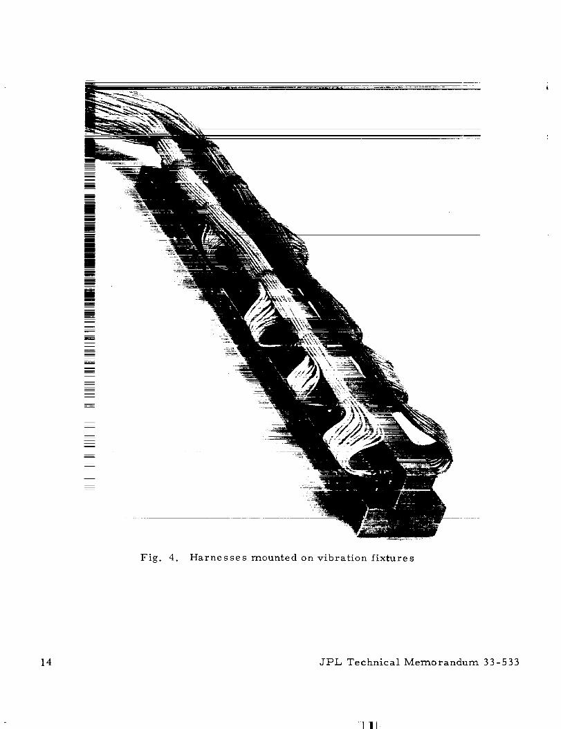
Fig. 4. Harnesses mounted on vibration fixtures
14 JPL Technical Memorandum 33-533
I li
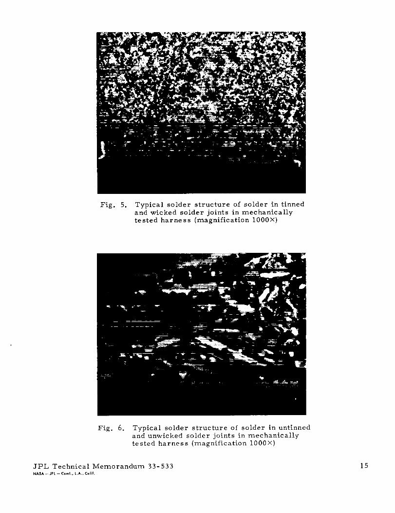
Fig. , Typical solder structure of solder in tinned
and wicked solder joints in mechanically
tested harness (magnification 1000×)
Fig. 6. Typical solder structure of solder in untinnedand unwicked solder joints in mechanically
tested harness (magnification 1000×)
JPL Technical Memorandum 33-533
NASA -- JPL -- Coral., L.A., Cal|f.
15

71F


!'FIi-