Introduction to Organic...
38
Introduction to Organic Electronics Introduction to Organic Electronics Marcus Halik Organic Materials & Devices www.omd.uni-erlangen.de University Erlangen-Nürnberg Martensstrasse 07 91058 Erlangen (GERMANY)
Transcript of Introduction to Organic...

Introduction to Organic ElectronicsIntroduction to Organic Electronics
Marcus Halik
Organic Materials & Deviceswww.omd.uni-erlangen.de
University Erlangen-NürnbergMartensstrasse 07
91058 Erlangen (GERMANY)

"Normally most people don't think of plastic as an electrical
conductor or semiconductor, but certain organic materials have amazing electronic properties"
Bengt
Nordén
-
Chairman of the Nobel Committee for Chemistry 2000
Alan J. Heeger, Alan G. MacDiarmid and Hideki ShirakawaNobel Prize in Chemistry 2000
Conductivity in Plastics

Ene
rgy
conduction band
valence band
Conductor –band overlap
metals (Cu, Al,…)
Semiconductor –small band gap
(Si: 1.12 eV)
tunable by doping
Insulator –large band gap
(diamond: 5.2 eV)
most organic materials
ΔE
Conductor, Semiconductor, Insulator

= e-
ΔE
valenceband
conduction band
ground state(charge compensated
by nuclear charge)
excitation charge transport
each electron leaves a hole in the valence bandelectrons and holes are movable by applying an external field
+ -
Generation and Transport of Charge

Structures in Organic MaterialsPolyethylene PE
(coiled 3D structure)Polyacetylene
(flat chain structure)
90°
C-C single bondtetrahedral geometry
C-C double bondplanar geometry

Extended Systems
binding energy (σ
-
bond) =
347 kJ/molbinding energy (π
–
bond) = 260 kJ/mol
Increasing the number of double bonds
Ethylene Butadiene
E
ΔE
LUMO
HOMO
~ 2 eV
Pentacene

n = 1 n = 2 n = 3 … n
HOMO
LUMO
valence band
π
π∗
Ener
gy Orbitals “BAND”
ΔE
Organic Semiconductors
Hydrocarbons with delocalized electrons –π-conjugation
**
n
conduction band

Organic Electronics
OFET (TFT)OLED solar cell OPV memory
molecular memory, diodes, transistors etc.
thin film devices
molecular devices

Organics vs. Silicon Technology
• independent from single crystalline substrates• low temperature processing• low complexity
• low performance• new technology - new processing required
Intel© Xenon PhiTM chip – 201262 core CPU – 22nm pitch(> 5.000.000.000 transistors)
first point contact Ge-transistor (Bell Labs - 1947)

Trends in Organic Electronics
molecular electronicsthin film electronics
large feature size – flexible substratesspecialties - limited volume
large volume – low performance
supplementary products
few nanometer feature size(e.g. Green et al. Nature 445 414 (2007)
“next generation” products
Samsung 2013

Examples
OFET (TFT)
OLED
solar cell OPV
flexible memory
electrochromic cellspolymer battery

Historic Milestones
1906: Photoconductivity in anthracene single-crystals discovered
1960: TCNQ with conductivity of 100 S/cm synthesized
1963: Electroluminescence in anthracene discovered
1973: Synthesis of the first true organic metal (TTF-TCNQ) reported
1977: Doping of polyacetylene demonstrated (2000 Nobel Prize)
1982: Organic thin film light emitting diode (OLED) demonstrated
1986: Organic field effect transistor demonstrated
1986: First efficient organic solar cell demonstrated
1995: Organic integrated circuits demonstrated
2004: Seiko-Epson demonstrates 40-inch OLED panel
2004 Graphene (Nobel Prize 2010)
2009 Samsung Galaxy with AMOLED
2009 Konarka OPV bagEpson

Cathode Anode
Tang et al., APL 51, 913 (1987)
hole transport layer
electrontransport
layer
Organic Light Emitting Diodes (1987)

Organic Solar Cell (1986)
Tang et al., APL 48, 183 (1986)
hole transportlayer electron transport
layer

Tsumura et al., APL 49, 1210 (1986)
Organic semiconductor
Heavily doped silicon wafer
Thermally grown SiO2 gate dielectric
Au Source Au Drain
Organic Field Effect Transistors (1986)
Transport on Different Length Scales
pixel devices(OLED, solar cell)
5 -100 nm
μm -
cm 1-
500 μm
< 5 nm
interface devices(transistor)
charge transport on nm-scalelow charier mobility required
charge transport on μm-scalelarge charier mobility required

Polymers vs. Small Molecules
Pentacene (twice sublimed)
Poly-3-hexylthiophene (regio-regular)
• charge transport along chain and by inter-chain hopping (lattice)
• deposition from solution (pot. printing)
• charge transport through ππ- stacking overlap
• deposition from vapor phase or solution
Polymers Small Molecules

0.8 nm
Poly-3-hexylthiopheneMn ~ 30.000 g/mollength (stretched) ~ 70 nmlength (coiled) ~ 20nm
mismatches in (3,5 or 3,4 position)average conjugation length is~ 10 - 15 repeat units (6 nm!!!)
Molecular Chain and Morphology
How can we transport charge over long distances (μm-range)????
~ 70 nm
~ 20 nm

μ
= 0.1 cm2/Vs μ
= 0.0002 cm2/Vs
Orientation - P3HT
Sirringhaus
et al. Nature 401,
685 (1999)
Lattice orientation dominates the polymer performancePerformance is limited by semi-crystalline behavior
Orientation depends on:• surface (treatment)• temperature• deposition method, …

• micron-size grains with terracing• efficient ππ-interaction (HOMO overlap)
Gundlach
et al., IEEE Electr. Dev. Lett. 18, 87 (1997) Knipp
et al., J. Appl. Phys. 93, 347 (2003)Troisi
et al. JCPB 109, 1849 (2005)
side top
E
How to Assemble Molecules ?
π-systems tend to self-organize (ππ-stacking)poly-crystalline films

“Order” as General Rule for Transport
H. Faber,, Adv. Mater. 21 (2009) 3099-3104
monolayer of Zink Oxide nanoparticles (diameter 5 nm)

x
y
Molecular Order and Charge Transport
amorphous polymer semi-crystalline polymer
thin film (small molecules)
organic single crystal
week interactionsome “contact points”un-isotropic transport
poor mobility
10-4 cm2/Vs
partial order ( , )coexistence crystallineand amorphous fraction
statistically un-isotropic transport
low mobility
~ 1
cm2/Vs
strong orderbreak in orientation(grain boundaries)
un-isotropic transportgood mobility
10
cm2/Vs
very strong orderno grain boundaries
strong isotropictransport
very good mobility
> 10
cm2/Vs

OLED - Display
(press release 27.06.2013: Samsungs first OLED TV- 1.40 m diagonal curved screen- ~ $ 9.000,-

Galaxy S4 full HD
OLED - Display
RGB – mixing (green down sized)smaller feature size 50 μm (resolution limit human eye)Full HD speedpower consumption

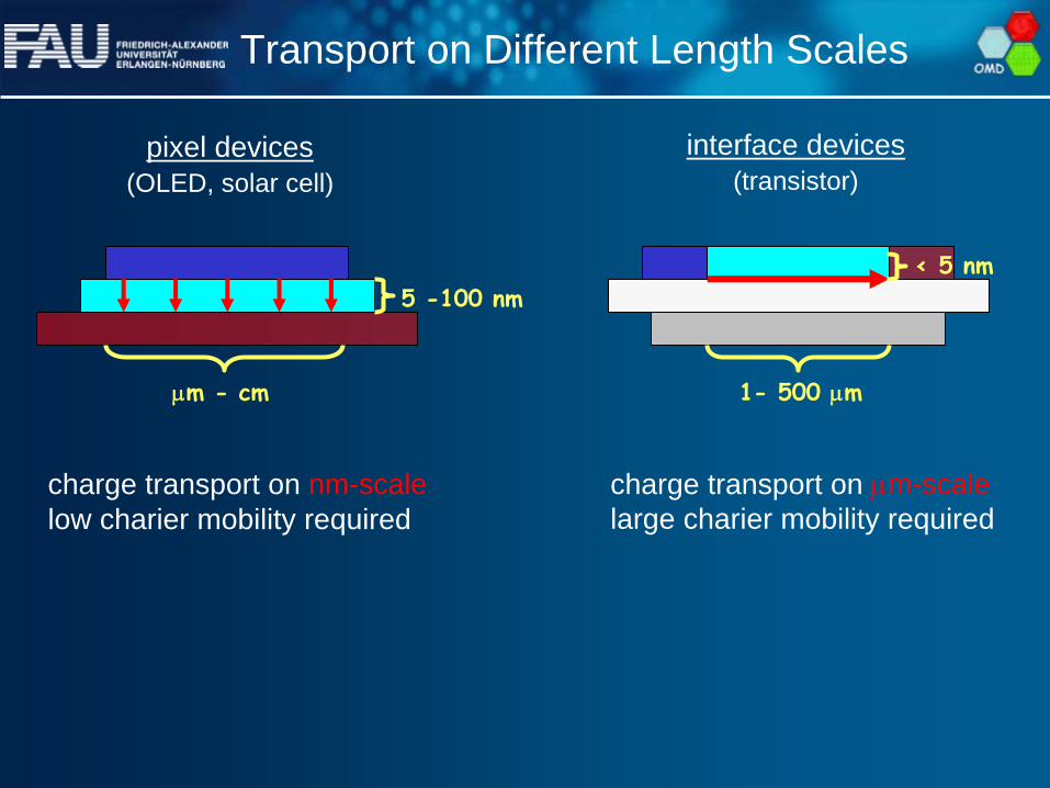
OLED - lighting
Mesta et al. Nature Materials 12, 652–658 (2013)
OLED - lighting
complex stack precise control of layer thicknesstunable colorlarge area, flexible substrateslong term stabilitypower consumption

OPV Approaches

cathode
anode
e--donor e--acceptor
dark currentlight current
h+ e-
I
V
VOC
•
••
ISC
MPP
FF
~ VOC
OPV – Bulk Hetero Junction
P = U x I PerformanceFF = PMPP /(VOC x ISC ) Fill Factor

OPV in a Contest

OPV – Future / Challenges
significant contribution to global energy demand (15 TW / year = 15 x 1012 W)
Heliatek
Modul-Efficiency !!!!! (VOC , ISC , FF)Cost/Watt – Price!!!!Stability, CO2 - footprint transparency

0 1 20
2x10⁻¹⁰
4x10⁻¹⁰
6x10⁻¹⁰
8x10⁻¹⁰
VGS = 0V to 1.5V (0.125V steps)
Drain-source voltage (V)D
rain
curr
ent(
A)
VGS
VDS
ID
Source Drain
Gate dielectric
Substrate
Organic semiconductor
Gate electrode
Channel
OTFT - electronic switch modulated by gate voltagedigital “0” and “1” state
ICs (RFID), backplanes (diplays, sensors)
electrical output characteristics
Organic Thin Film Transistor
“0”
“1”

Important Electrical Parameter
a) Carrier mobility μ
= 0.5 cm2/Vsb) Threshold Voltage VTH = -3 Vc) Subthreshold slope 0.2 V/decaded) On/off current ratio 108a
b•
c d
transfer characteristics
“0”
“1” W/L (100μm/10μm) = 10
W/L (1000μm/10μm)= 100
ID
=1
2μeff
Ci
W
L(VG
-VT
)2

Flexible backplanes for OLED, E-Ink
homogeneous large currentsYield = 100 %
Application Fields
Sensor backplanes with integrated memory
homogeneous large currentsLong retention
Sekitani Science 2009

ICs – Dice (Simple Game)
Full logic &graphics driver in
organic electronics on plastics
Application board
Input - “start” game
Gate Count3 D-FlipFlops = 27 NANDs1 OR = 3 NANDs1 NAND = 1 NANDTotal = 31 NANDs
= 155 TFTs
Device
Circuit layout
Output - LED
Operation -
Game

Current - Mobility Speed – Mobility, Dimensions
Large mobility > 10 cm2/VsDisplay backplane
Speed larger 200 kHz (display)13.56 MHz (ICs e.g. RFID)
OTFT Challenges

Performance: a) film thickness control and homogeneityb) spatial resolution
extremely high:multilayer,interfaces,contact doping,carrier balance (< 3 nm)uncritical to high:large area devicesPixel x0 μm2 440ppiLighting cm2/m2
OLED TFTs OPV NVM
extremely high:interfaces,driving voltage,order(~ 5 nm)
high:channel length ~ speedS/G overlap few μm
uncritical:blendself-organizedinterfaces,absorption
uncritical:large area devicessupply/draincm2
high:write-erase-read voltage,signal ratio
uncritical –extremely high:integration density
Boundary Conditions
Suitable performance depends critically on control of dimensions and interfaces on nanometer scale
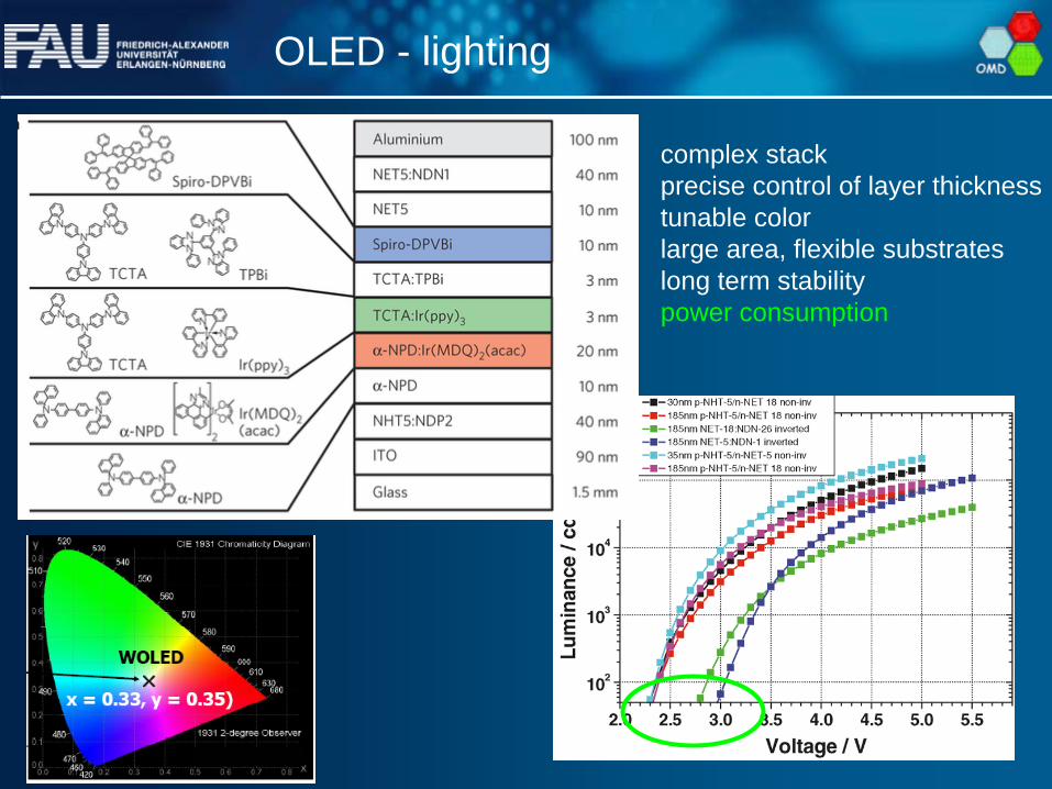
Technical Approaches in Thin Film Processing
throughput/expensesfilm homogeneity/ spatial resolution
approach
spin coating/spray coating excellent/ poor batch/
large area
printing (μ-CP, ink jet)
resolution ~ speed-1
medium area
PVD, CVD
critical/ good
excellent/ poor good / complex
T. Sekitani
et al. PNAS. 105, (2008) 4976-4980

Polyethylene terephthalate (PET)• Tg ~ 80°C, Tm ~ 250°C
Paper• multi component substrate• ∅
fiber ~ 10 – 20 mm
Polyethylene naphthalate (PEN)• Tg ~ 120°C, Tm ~ 265°C
Glass• smooth surface, rigid
Electronics everywhere
Sounds good – but (thermal, mechanical, solvent, optical stability;barrier properties, adhesion, costs)
Also: stainless steel, textiles
20 μm