Introduction to FPGA Design Illustrating the FPGA design process using Quartus II design software...
30
Introduction to FPGA Design Illustrating the FPGA design process using Quartus II design software and the Cyclone II FPGA Starter Board. Physics 536 – Spring 2009
-
Upload
gavin-neal -
Category
Documents
-
view
241 -
download
3
Transcript of Introduction to FPGA Design Illustrating the FPGA design process using Quartus II design software...

Introduction to FPGA Design
Illustrating the FPGA design process using Quartus II design software and the Cyclone II
FPGA Starter Board.
Physics 536 – Spring 2009

Why FPGA’s?• Digital logic:
– Equivalent to a large number of discrete logic elements– NOT a microprocessor (although microprocessors can be
implemented in an FPGA design)
• High density:– All the logic is inside a single chip– No need for interconnecting traces on PCB between logic
circuits
• Reprogrammable:– Designs can be changed after the hardware has been
manufactured– High-level design software optimizes the usage of limited
resources

FPGA Resources
• Both companies produce competitive products – neither is endorsed. Other companies exist...
• We use Altera tools to demonstrate the design process.
• Xilinx has a similar set of tools.• Conceptually, the design process is the same.
Cyclone II FPGA Starter BoardAltera
EP2C20F484C7N
$56.30 from Digi-Key
Configuration device – stores the design that is automatically downloaded when power is applied.
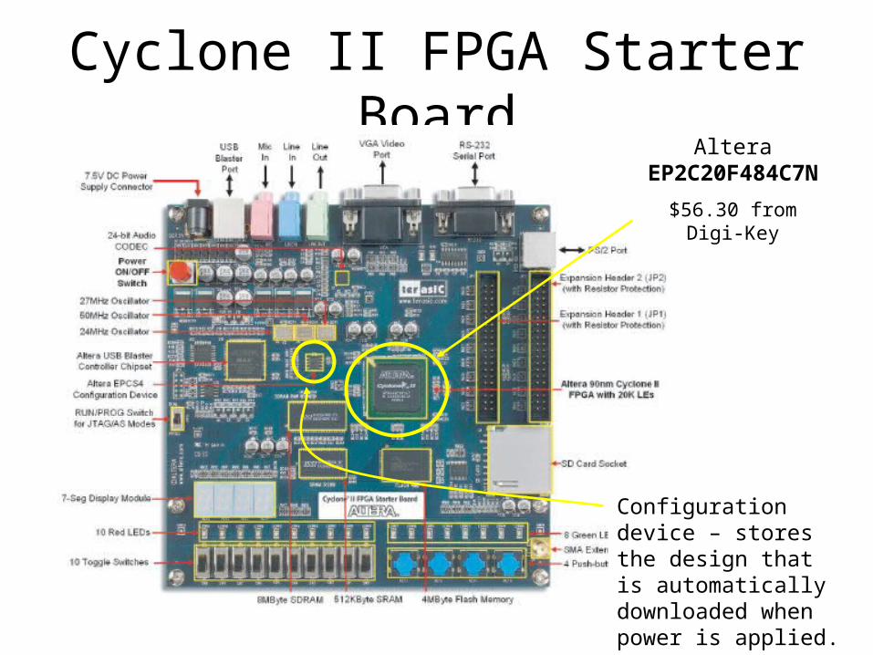
Example Design Problem
• Implement a 4-input XOR function:– Output will be high only when exactly one
input is high.– Use KEY[0..3] as inputs.– Show output on green LED.
• Boolean algebra:
• We could simplify this, but choose not to.
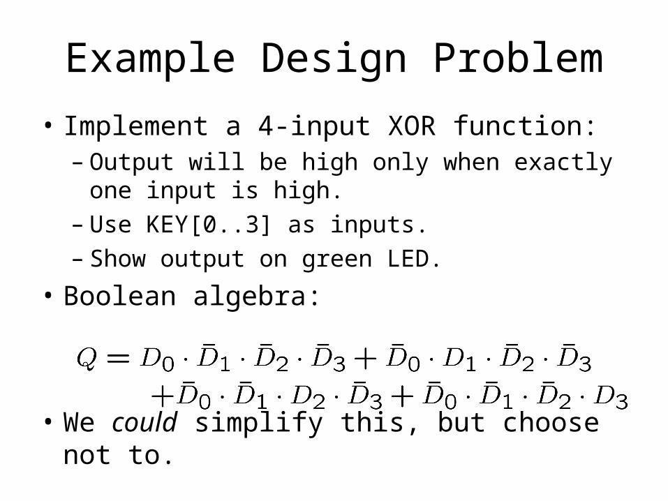
Design Flow
• Design entry:– Schematic entry– High level language
• Synthesis:– Translating design into
logic elements
• Simulation:– Validate design logic
• Fitting:– Implementing logic using
FPGA resources
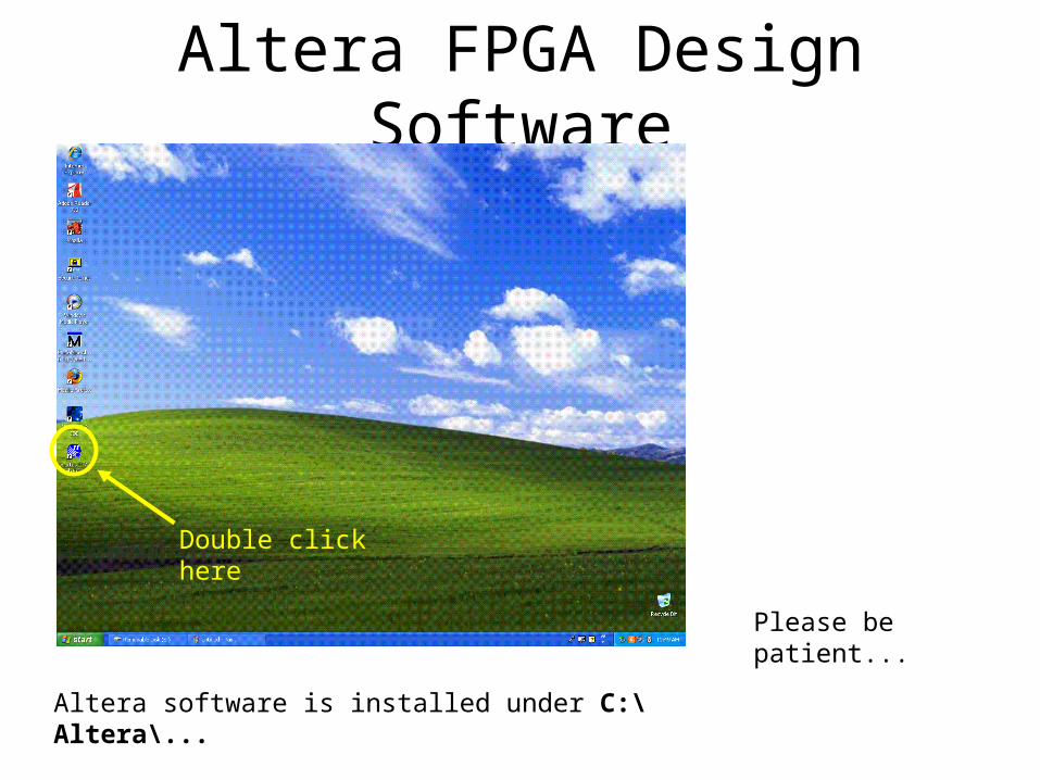
Altera FPGA Design Software
Double click here
Altera software is installed under C:\Altera\...
Please be patient...
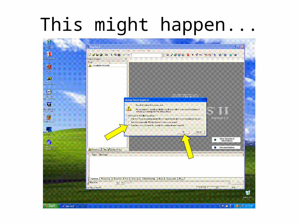
This might happen...
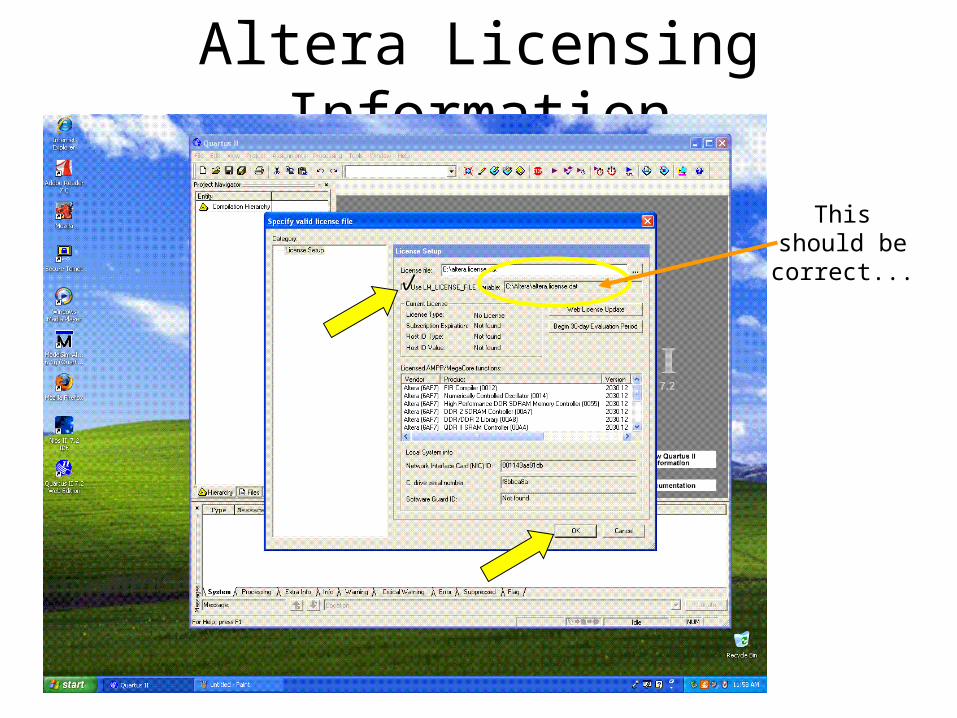
Altera Licensing Information
This should be correct...
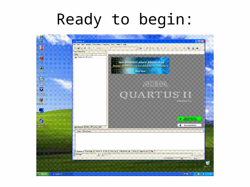
Ready to begin:
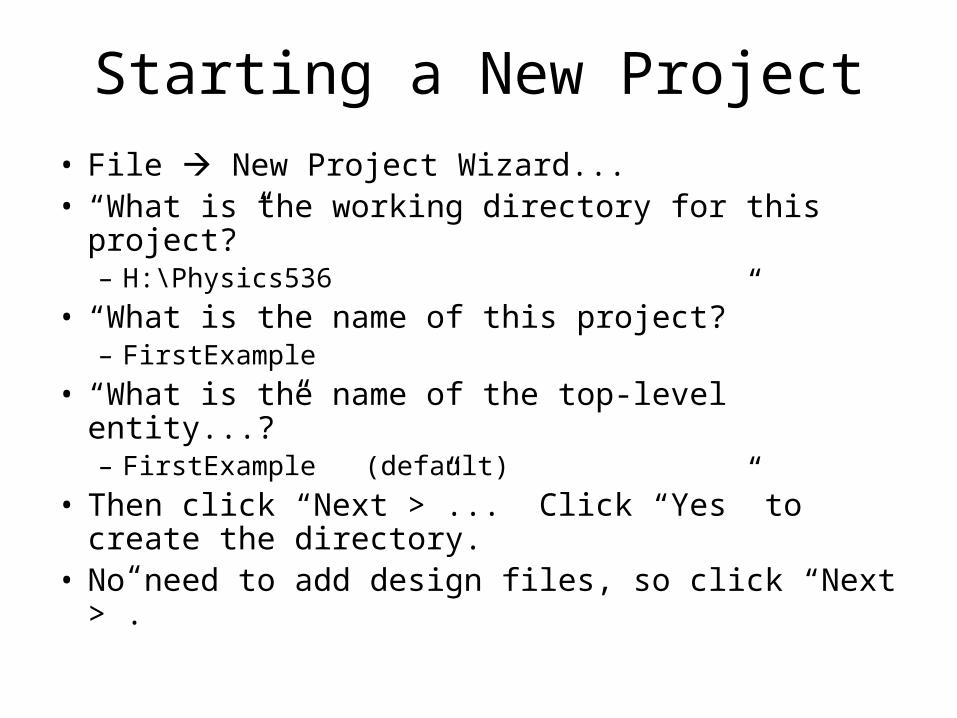
Starting a New Project
• File New Project Wizard...• “What is the working directory for this project?”
– H:\Physics536
• “What is the name of this project?”– FirstExample
• “What is the name of the top-level entity...?”– FirstExample (default)
• Then click “Next >”... Click “Yes” to create the directory.
• No need to add design files, so click “Next >”.
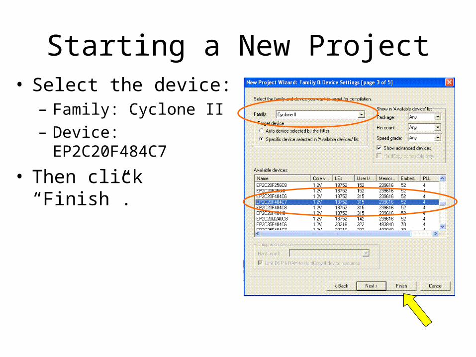
Starting a New Project• Select the device:
– Family: Cyclone II– Device: EP2C20F484C7
• Then click “Finish”.
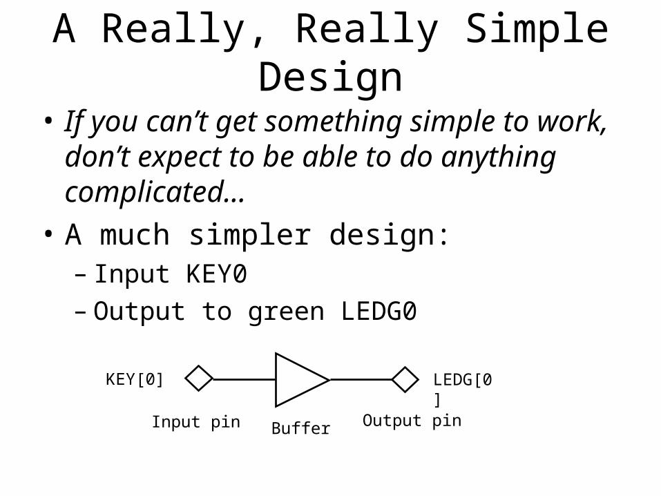
A Really, Really Simple Design
• If you can’t get something simple to work, don’t expect to be able to do anything complicated...
• A much simpler design:– Input KEY0– Output to green LEDG0
KEY[0] LEDG[0]
Input pin Output pinBuffer
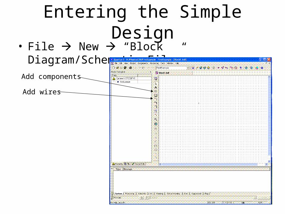
Entering the Simple Design• File New “Block Diagram/Schematic File”
Add components
Add wires
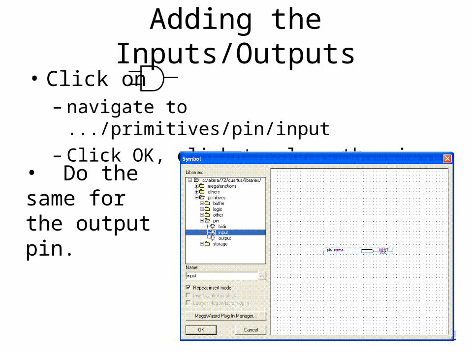
Adding the Inputs/Outputs• Click on
– navigate to .../primitives/pin/input– Click OK, click to place the pin.
• Do the same for the output pin.
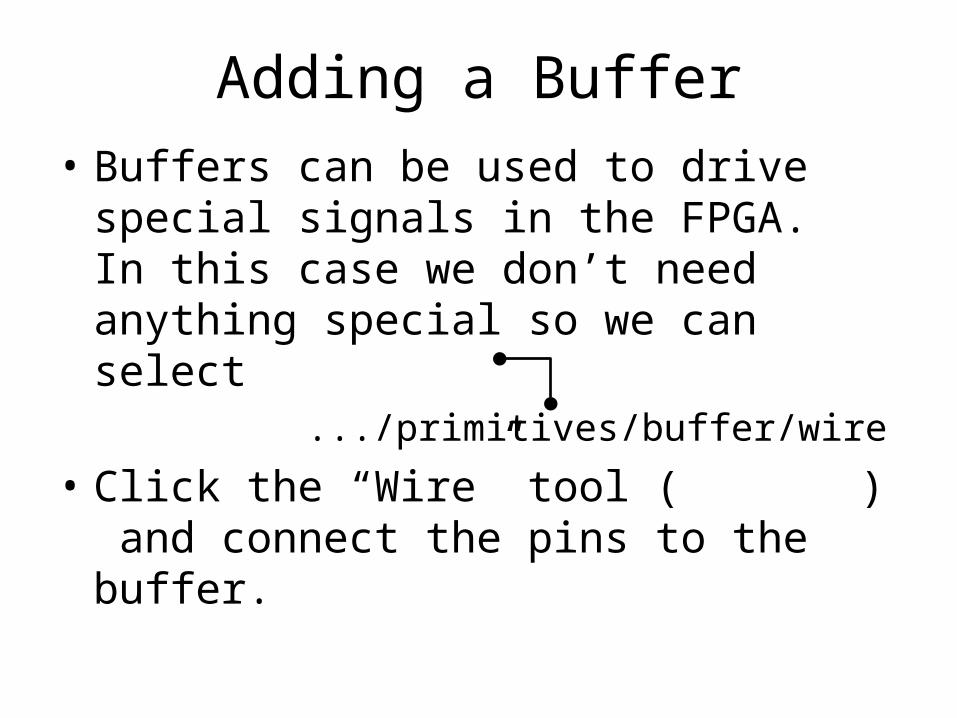
Adding a Buffer• Buffers can be used to drive special
signals in the FPGA. In this case we don’t need anything special so we can select .../primitives/buffer/wire
• Click the “Wire” tool ( ) and connect the pins to the buffer.
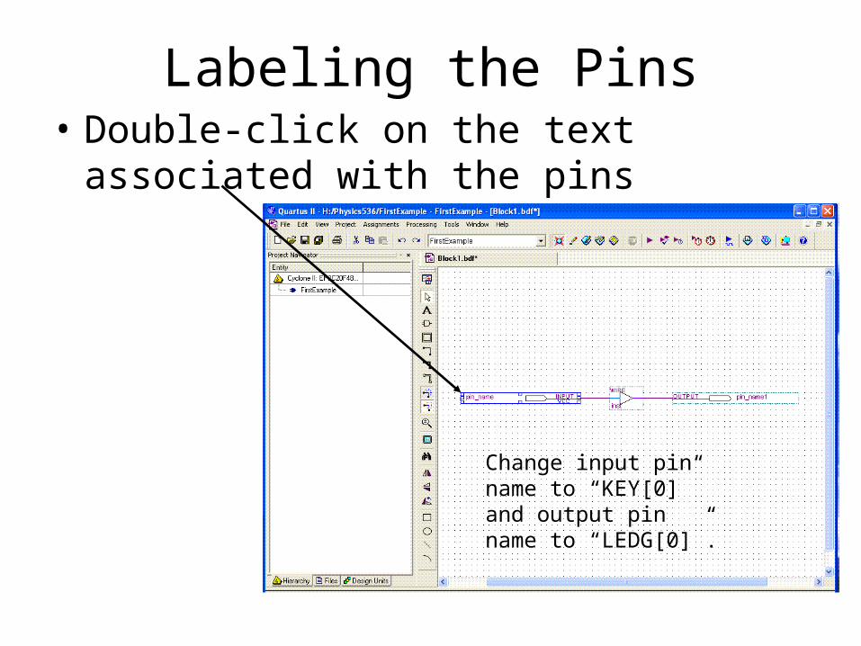
Labeling the Pins• Double-click on the text associated with
the pins
Change input pin name to “KEY[0]” and output pin name to “LEDG[0]”.
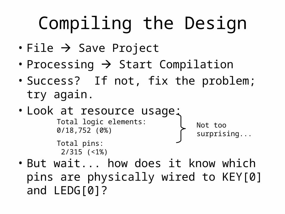
Compiling the Design• File Save Project
• Processing Start Compilation
• Success? If not, fix the problem; try again.
• Look at resource usage:
• But wait... how does it know which pins are physically wired to KEY[0] and LEDG[0]?
Total logic elements: 0/18,752 (0%)
Total pins: 2/315 (<1%)Not too surprising...
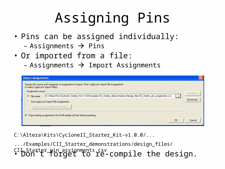
Assigning Pins• Pins can be assigned individually:
– Assignments Pins
• Or imported from a file:– Assignments Import Assignments
• Don’t forget to re-compile the design.
C:\Altera\Kits\CycloneII_Starter_Kit-v1.0.0/...
.../Examples/CII_Starter_demonstrations/design_files/CII_Starter_pin_assignments.csv
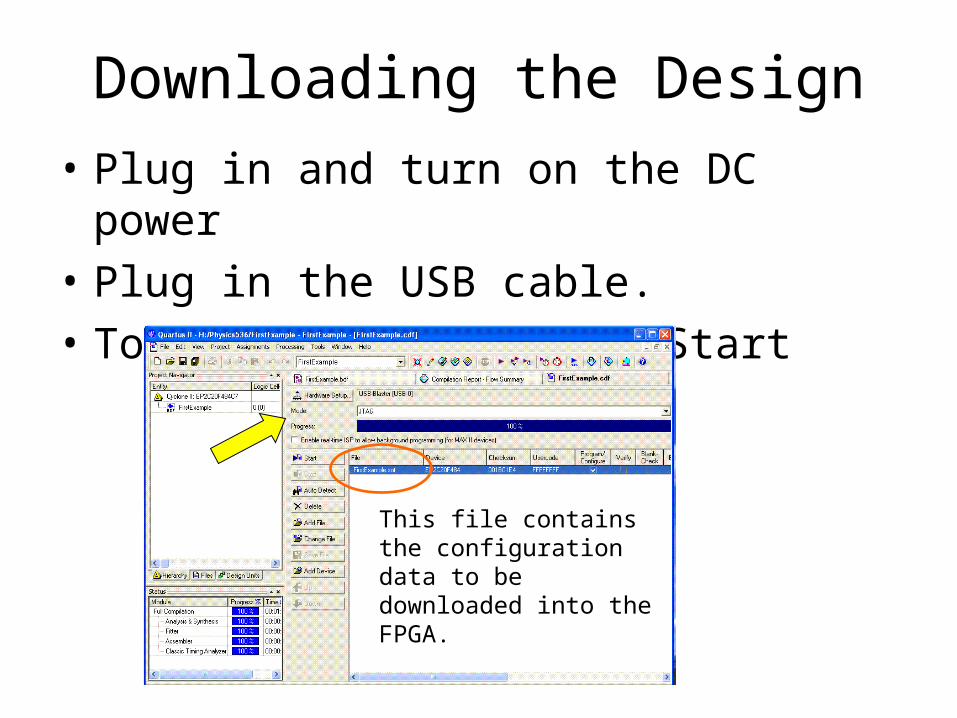
Downloading the Design
• Plug in and turn on the DC power
• Plug in the USB cable.
• Tools Programmer Start
This file contains the configuration data to be downloaded into the FPGA.
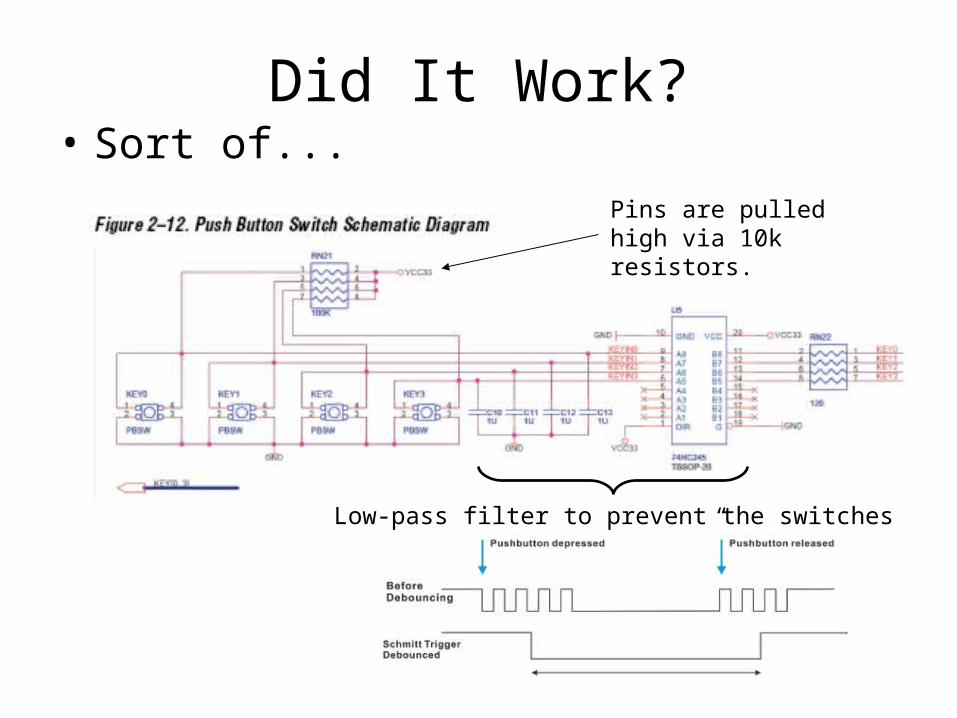
Did It Work?• Sort of...
Pins are pulled high via 10k resistors.
Low-pass filter to prevent the switches from “bouncing”.

4-Input XOR
• Invert the KEY[0..3] inputs before assigning them to D0, D1, D2, D3.
• Use .../primitives/logic/not for inverter• Implement the logic:
• Use 4-input AND and 4-input OR gates:– .../primitives/logic/and4– .../primitives/logic/or4
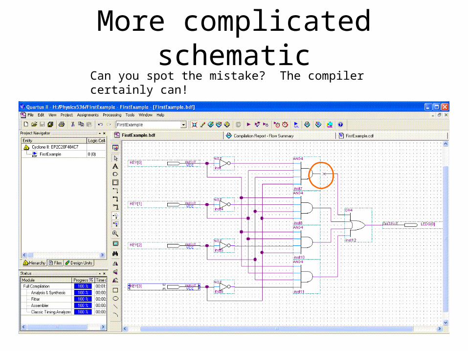
More complicated schematicCan you spot the mistake? The compiler certainly can!
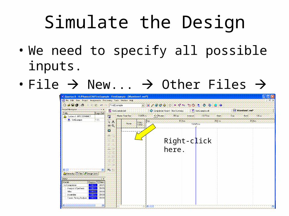
Simulate the Design
• We need to specify all possible inputs.
• File New... Other Files Waveform Vector File
Right-click here.
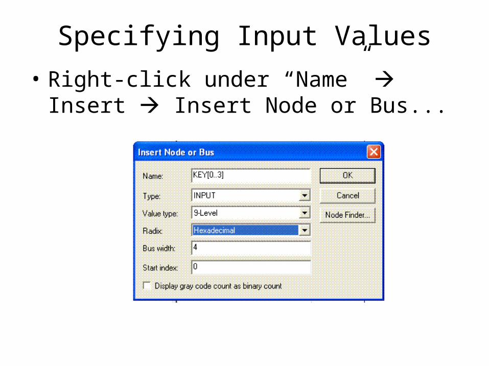
Specifying Input Values
• Right-click under “Name” Insert Insert Node or Bus...
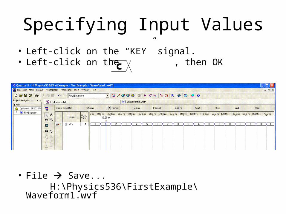
Specifying Input Values
• Left-click on the “KEY” signal.• Left-click on the , then OK
• File Save... H:\Physics536\FirstExample\Waveform1.wvf
c
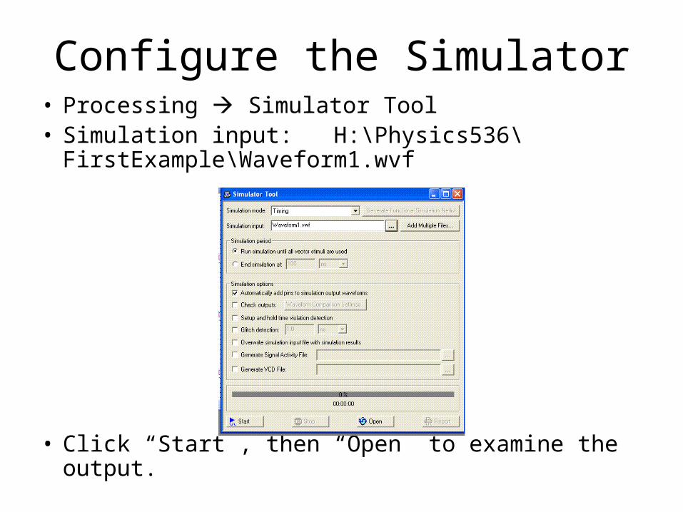
Configure the Simulator• Processing Simulator Tool• Simulation input: H:\Physics536\FirstExample\
Waveform1.wvf
• Click “Start”, then “Open” to examine the output.
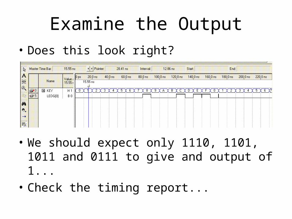
Examine the Output
• Does this look right?
• We should expect only 1110, 1101, 1011 and 0111 to give and output of 1...
• Check the timing report...
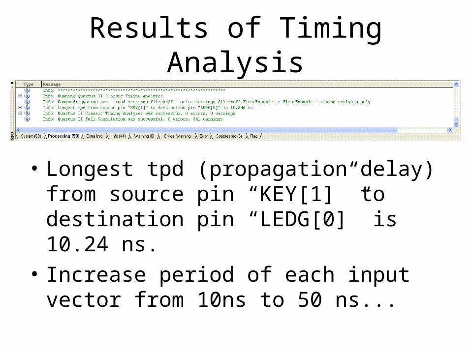
Results of Timing Analysis
• Longest tpd (propagation delay) from source pin “KEY[1]” to destination pin “LEDG[0]” is 10.24 ns.
• Increase period of each input vector from 10ns to 50 ns...
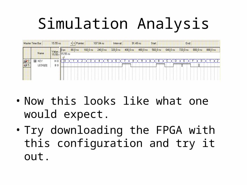
Simulation Analysis
• Now this looks like what one would expect.
• Try downloading the FPGA with this configuration and try it out.