Introduction to Circuit Components -...
238
Advanced Design System 2011.01 - Introduction to Circuit Components 1 Advanced Design System 2011.01 Feburary 2011 Introduction to Circuit Components
Transcript of Introduction to Circuit Components -...

Advanced Design System 2011.01 - Introduction to Circuit Components
1
Advanced Design System 2011.01
Feburary 2011Introduction to Circuit Components

Advanced Design System 2011.01 - Introduction to Circuit Components
2
© Agilent Technologies, Inc. 2000-20115301 Stevens Creek Blvd., Santa Clara, CA 95052 USANo part of this documentation may be reproduced in any form or by any means (includingelectronic storage and retrieval or translation into a foreign language) without prioragreement and written consent from Agilent Technologies, Inc. as governed by UnitedStates and international copyright laws.
AcknowledgmentsMentor Graphics is a trademark of Mentor Graphics Corporation in the U.S. and othercountries. Mentor products and processes are registered trademarks of Mentor GraphicsCorporation. * Calibre is a trademark of Mentor Graphics Corporation in the US and othercountries. "Microsoft®, Windows®, MS Windows®, Windows NT®, Windows 2000® andWindows Internet Explorer® are U.S. registered trademarks of Microsoft Corporation.Pentium® is a U.S. registered trademark of Intel Corporation. PostScript® and Acrobat®are trademarks of Adobe Systems Incorporated. UNIX® is a registered trademark of theOpen Group. Oracle and Java and registered trademarks of Oracle and/or its affiliates.Other names may be trademarks of their respective owners. SystemC® is a registeredtrademark of Open SystemC Initiative, Inc. in the United States and other countries and isused with permission. MATLAB® is a U.S. registered trademark of The Math Works, Inc..HiSIM2 source code, and all copyrights, trade secrets or other intellectual property rightsin and to the source code in its entirety, is owned by Hiroshima University and STARC.FLEXlm is a trademark of Globetrotter Software, Incorporated. Layout Boolean Engine byKlaas Holwerda, v1.7 http://www.xs4all.nl/~kholwerd/bool.html . FreeType Project,Copyright (c) 1996-1999 by David Turner, Robert Wilhelm, and Werner Lemberg.QuestAgent search engine (c) 2000-2002, JObjects. Motif is a trademark of the OpenSoftware Foundation. Netscape is a trademark of Netscape Communications Corporation.Netscape Portable Runtime (NSPR), Copyright (c) 1998-2003 The Mozilla Organization. Acopy of the Mozilla Public License is at http://www.mozilla.org/MPL/ . FFTW, The FastestFourier Transform in the West, Copyright (c) 1997-1999 Massachusetts Institute ofTechnology. All rights reserved.
The following third-party libraries are used by the NlogN Momentum solver:
"This program includes Metis 4.0, Copyright © 1998, Regents of the University ofMinnesota", http://www.cs.umn.edu/~metis , METIS was written by George Karypis([email protected]).
Intel@ Math Kernel Library, http://www.intel.com/software/products/mkl
SuperLU_MT version 2.0 - Copyright © 2003, The Regents of the University of California,through Lawrence Berkeley National Laboratory (subject to receipt of any requiredapprovals from U.S. Dept. of Energy). All rights reserved. SuperLU Disclaimer: THISSOFTWARE IS PROVIDED BY THE COPYRIGHT HOLDERS AND CONTRIBUTORS "AS IS"AND ANY EXPRESS OR IMPLIED WARRANTIES, INCLUDING, BUT NOT LIMITED TO, THEIMPLIED WARRANTIES OF MERCHANTABILITY AND FITNESS FOR A PARTICULAR PURPOSEARE DISCLAIMED. IN NO EVENT SHALL THE COPYRIGHT OWNER OR CONTRIBUTORS BELIABLE FOR ANY DIRECT, INDIRECT, INCIDENTAL, SPECIAL, EXEMPLARY, ORCONSEQUENTIAL DAMAGES (INCLUDING, BUT NOT LIMITED TO, PROCUREMENT OFSUBSTITUTE GOODS OR SERVICES; LOSS OF USE, DATA, OR PROFITS; OR BUSINESSINTERRUPTION) HOWEVER CAUSED AND ON ANY THEORY OF LIABILITY, WHETHER INCONTRACT, STRICT LIABILITY, OR TORT (INCLUDING NEGLIGENCE OR OTHERWISE)ARISING IN ANY WAY OUT OF THE USE OF THIS SOFTWARE, EVEN IF ADVISED OF THE

Advanced Design System 2011.01 - Introduction to Circuit Components
3
POSSIBILITY OF SUCH DAMAGE.
7-zip - 7-Zip Copyright: Copyright (C) 1999-2009 Igor Pavlov. Licenses for files are:7z.dll: GNU LGPL + unRAR restriction, All other files: GNU LGPL. 7-zip License: This libraryis free software; you can redistribute it and/or modify it under the terms of the GNULesser General Public License as published by the Free Software Foundation; eitherversion 2.1 of the License, or (at your option) any later version. This library is distributedin the hope that it will be useful,but WITHOUT ANY WARRANTY; without even the impliedwarranty of MERCHANTABILITY or FITNESS FOR A PARTICULAR PURPOSE. See the GNULesser General Public License for more details. You should have received a copy of theGNU Lesser General Public License along with this library; if not, write to the FreeSoftware Foundation, Inc., 59 Temple Place, Suite 330, Boston, MA 02111-1307 USA.unRAR copyright: The decompression engine for RAR archives was developed using sourcecode of unRAR program.All copyrights to original unRAR code are owned by AlexanderRoshal. unRAR License: The unRAR sources cannot be used to re-create the RARcompression algorithm, which is proprietary. Distribution of modified unRAR sources inseparate form or as a part of other software is permitted, provided that it is clearly statedin the documentation and source comments that the code may not be used to develop aRAR (WinRAR) compatible archiver. 7-zip Availability: http://www.7-zip.org/
AMD Version 2.2 - AMD Notice: The AMD code was modified. Used by permission. AMDcopyright: AMD Version 2.2, Copyright © 2007 by Timothy A. Davis, Patrick R. Amestoy,and Iain S. Duff. All Rights Reserved. AMD License: Your use or distribution of AMD or anymodified version of AMD implies that you agree to this License. This library is freesoftware; you can redistribute it and/or modify it under the terms of the GNU LesserGeneral Public License as published by the Free Software Foundation; either version 2.1 ofthe License, or (at your option) any later version. This library is distributed in the hopethat it will be useful, but WITHOUT ANY WARRANTY; without even the implied warranty ofMERCHANTABILITY or FITNESS FOR A PARTICULAR PURPOSE. See the GNU LesserGeneral Public License for more details. You should have received a copy of the GNULesser General Public License along with this library; if not, write to the Free SoftwareFoundation, Inc., 51 Franklin St, Fifth Floor, Boston, MA 02110-1301 USA Permission ishereby granted to use or copy this program under the terms of the GNU LGPL, providedthat the Copyright, this License, and the Availability of the original version is retained onall copies.User documentation of any code that uses this code or any modified version ofthis code must cite the Copyright, this License, the Availability note, and "Used bypermission." Permission to modify the code and to distribute modified code is granted,provided the Copyright, this License, and the Availability note are retained, and a noticethat the code was modified is included. AMD Availability:http://www.cise.ufl.edu/research/sparse/amd
UMFPACK 5.0.2 - UMFPACK Notice: The UMFPACK code was modified. Used by permission.UMFPACK Copyright: UMFPACK Copyright © 1995-2006 by Timothy A. Davis. All RightsReserved. UMFPACK License: Your use or distribution of UMFPACK or any modified versionof UMFPACK implies that you agree to this License. This library is free software; you canredistribute it and/or modify it under the terms of the GNU Lesser General Public Licenseas published by the Free Software Foundation; either version 2.1 of the License, or (atyour option) any later version. This library is distributed in the hope that it will be useful,but WITHOUT ANY WARRANTY; without even the implied warranty of MERCHANTABILITYor FITNESS FOR A PARTICULAR PURPOSE. See the GNU Lesser General Public License formore details. You should have received a copy of the GNU Lesser General Public Licensealong with this library; if not, write to the Free Software Foundation, Inc., 51 Franklin St,Fifth Floor, Boston, MA 02110-1301 USA Permission is hereby granted to use or copy this

Advanced Design System 2011.01 - Introduction to Circuit Components
4
program under the terms of the GNU LGPL, provided that the Copyright, this License, andthe Availability of the original version is retained on all copies. User documentation of anycode that uses this code or any modified version of this code must cite the Copyright, thisLicense, the Availability note, and "Used by permission." Permission to modify the codeand to distribute modified code is granted, provided the Copyright, this License, and theAvailability note are retained, and a notice that the code was modified is included.UMFPACK Availability: http://www.cise.ufl.edu/research/sparse/umfpack UMFPACK(including versions 2.2.1 and earlier, in FORTRAN) is available athttp://www.cise.ufl.edu/research/sparse . MA38 is available in the Harwell SubroutineLibrary. This version of UMFPACK includes a modified form of COLAMD Version 2.0,originally released on Jan. 31, 2000, also available athttp://www.cise.ufl.edu/research/sparse . COLAMD V2.0 is also incorporated as a built-infunction in MATLAB version 6.1, by The MathWorks, Inc. http://www.mathworks.com .COLAMD V1.0 appears as a column-preordering in SuperLU (SuperLU is available athttp://www.netlib.org ). UMFPACK v4.0 is a built-in routine in MATLAB 6.5. UMFPACK v4.3is a built-in routine in MATLAB 7.1.
Qt Version 4.6.3 - Qt Notice: The Qt code was modified. Used by permission. Qt copyright:Qt Version 4.6.3, Copyright (c) 2010 by Nokia Corporation. All Rights Reserved. QtLicense: Your use or distribution of Qt or any modified version of Qt implies that you agreeto this License. This library is free software; you can redistribute it and/or modify it undertheterms of the GNU Lesser General Public License as published by the Free SoftwareFoundation; either version 2.1 of the License, or (at your option) any later version. Thislibrary is distributed in the hope that it will be useful,but WITHOUT ANY WARRANTY; without even the implied warranty of MERCHANTABILITYor FITNESS FOR A PARTICULAR PURPOSE. See the GNU Lesser General Public License formore details. You should have received a copy of the GNU Lesser General Public Licensealong with this library; if not, write to the Free Software Foundation, Inc., 51 Franklin St,Fifth Floor, Boston, MA 02110-1301 USA Permission is hereby granted to use or copy thisprogram under the terms of the GNU LGPL, provided that the Copyright, this License, andthe Availability of the original version is retained on all copies.Userdocumentation of any code that uses this code or any modified version of this code mustcite the Copyright, this License, the Availability note, and "Used by permission."Permission to modify the code and to distribute modified code is granted, provided theCopyright, this License, and the Availability note are retained, and a notice that the codewas modified is included. Qt Availability: http://www.qtsoftware.com/downloads PatchesApplied to Qt can be found in the installation at:$HPEESOF_DIR/prod/licenses/thirdparty/qt/patches. You may also contact BrianBuchanan at Agilent Inc. at [email protected] for more information.
The HiSIM_HV source code, and all copyrights, trade secrets or other intellectual propertyrights in and to the source code, is owned by Hiroshima University and/or STARC.
Errata The ADS product may contain references to "HP" or "HPEESOF" such as in filenames and directory names. The business entity formerly known as "HP EEsof" is now partof Agilent Technologies and is known as "Agilent EEsof". To avoid broken functionality andto maintain backward compatibility for our customers, we did not change all the namesand labels that contain "HP" or "HPEESOF" references.
Warranty The material contained in this document is provided "as is", and is subject tobeing changed, without notice, in future editions. Further, to the maximum extentpermitted by applicable law, Agilent disclaims all warranties, either express or implied,

Advanced Design System 2011.01 - Introduction to Circuit Components
5
with regard to this documentation and any information contained herein, including but notlimited to the implied warranties of merchantability and fitness for a particular purpose.Agilent shall not be liable for errors or for incidental or consequential damages inconnection with the furnishing, use, or performance of this document or of anyinformation contained herein. Should Agilent and the user have a separate writtenagreement with warranty terms covering the material in this document that conflict withthese terms, the warranty terms in the separate agreement shall control.
Technology Licenses The hardware and/or software described in this document arefurnished under a license and may be used or copied only in accordance with the terms ofsuch license. Portions of this product include the SystemC software licensed under OpenSource terms, which are available for download at http://systemc.org/ . This software isredistributed by Agilent. The Contributors of the SystemC software provide this software"as is" and offer no warranty of any kind, express or implied, including without limitationwarranties or conditions or title and non-infringement, and implied warranties orconditions merchantability and fitness for a particular purpose. Contributors shall not beliable for any damages of any kind including without limitation direct, indirect, special,incidental and consequential damages, such as lost profits. Any provisions that differ fromthis disclaimer are offered by Agilent only.
Restricted Rights Legend U.S. Government Restricted Rights. Software and technicaldata rights granted to the federal government include only those rights customarilyprovided to end user customers. Agilent provides this customary commercial license inSoftware and technical data pursuant to FAR 12.211 (Technical Data) and 12.212(Computer Software) and, for the Department of Defense, DFARS 252.227-7015(Technical Data - Commercial Items) and DFARS 227.7202-3 (Rights in CommercialComputer Software or Computer Software Documentation).
Advanced Design System 2011.01 - Introduction to Circuit Components
6
Circuit Components . . . . . . . . . . . . . . . . . . . . . . . . . . . . . . . . . . . . . . . . . . . . . . . . . . . . . . 9 Introduction . . . . . . . . . . . . . . . . . . . . . . . . . . . . . . . . . . . . . . . . . . . . . . . . . . . . . . . . . . 10 Bin Model (Bin Model for Automatic Model Selection) . . . . . . . . . . . . . . . . . . . . . . . . . . . . . . 11 FORMAT A, B, C, D, E Drawing Formats . . . . . . . . . . . . . . . . . . . . . . . . . . . . . . . . . . . . . . . 14 Ground (Ground Component) . . . . . . . . . . . . . . . . . . . . . . . . . . . . . . . . . . . . . . . . . . . . . . 15 Multiplicity Parameter _M . . . . . . . . . . . . . . . . . . . . . . . . . . . . . . . . . . . . . . . . . . . . . . . . . 16 Series IV or MDS Product Migration Components . . . . . . . . . . . . . . . . . . . . . . . . . . . . . . . . . 18 Term (Port Impedance for S-parameters) . . . . . . . . . . . . . . . . . . . . . . . . . . . . . . . . . . . . . . 21
Data File Components . . . . . . . . . . . . . . . . . . . . . . . . . . . . . . . . . . . . . . . . . . . . . . . . . . . . . 22 DataAccessComponent (Data Access Component) . . . . . . . . . . . . . . . . . . . . . . . . . . . . . . . . 23 De_Embed/De_EmbedSnP (2-Port to 12-Port De-Embed Data File) . . . . . . . . . . . . . . . . . . . . 37 Deembed1 (1-Port De-Embed Data File) . . . . . . . . . . . . . . . . . . . . . . . . . . . . . . . . . . . . . . 46 Deembed2 (2-Port De-Embed File) . . . . . . . . . . . . . . . . . . . . . . . . . . . . . . . . . . . . . . . . . . 48 Deembed4 (4-Port De-Embed Data File) . . . . . . . . . . . . . . . . . . . . . . . . . . . . . . . . . . . . . . 50 Deembed6 (6-Port De-Embed Data File) . . . . . . . . . . . . . . . . . . . . . . . . . . . . . . . . . . . . . . 52 Deembed8 (8-Port De-Embed Data File) . . . . . . . . . . . . . . . . . . . . . . . . . . . . . . . . . . . . . . 54 Deembed12 (12-Port De-Embed Data File) . . . . . . . . . . . . . . . . . . . . . . . . . . . . . . . . . . . . . 56 NetlistInclude (Netlist File Include Component) . . . . . . . . . . . . . . . . . . . . . . . . . . . . . . . . . . 58 S1P (1-Port S-parameter File) . . . . . . . . . . . . . . . . . . . . . . . . . . . . . . . . . . . . . . . . . . . . . . 62 S2P (2-Port S-parameter File) . . . . . . . . . . . . . . . . . . . . . . . . . . . . . . . . . . . . . . . . . . . . . . 64 S2P Conn (2-Port S-parameter File; connector artwork) . . . . . . . . . . . . . . . . . . . . . . . . . . . . 67 S2PMDIF (Multi-Dimensional 2-Port S-parameter File) . . . . . . . . . . . . . . . . . . . . . . . . . . . . . 69 S2P_Pad3 (2-Port S-parameter File; pad artwork) . . . . . . . . . . . . . . . . . . . . . . . . . . . . . . . . 71 S2P_Spac (2-Port S-parameter File) . . . . . . . . . . . . . . . . . . . . . . . . . . . . . . . . . . . . . . . . . 73 S3P (3-Port S-parameter File) . . . . . . . . . . . . . . . . . . . . . . . . . . . . . . . . . . . . . . . . . . . . . . 75 S4P (4-Port S-parameter File) . . . . . . . . . . . . . . . . . . . . . . . . . . . . . . . . . . . . . . . . . . . . . . 78 S5P to S9P (5-Port to 9-Port S-parameter File) . . . . . . . . . . . . . . . . . . . . . . . . . . . . . . . . . . 81 S10P to S20P (10-Port to 20-Port S-parameter File) . . . . . . . . . . . . . . . . . . . . . . . . . . . . . . 84 S21P to S99P (21-Port to 99-Port S-parameter File) . . . . . . . . . . . . . . . . . . . . . . . . . . . . . . 87 SnP component (n>99) . . . . . . . . . . . . . . . . . . . . . . . . . . . . . . . . . . . . . . . . . . . . . . . . . . 90 SnP_Diff component . . . . . . . . . . . . . . . . . . . . . . . . . . . . . . . . . . . . . . . . . . . . . . . . . . . . 93 VAR (Variables and Equations Component) . . . . . . . . . . . . . . . . . . . . . . . . . . . . . . . . . . . . . 96 W_Element (Multi-Conductor Transmission Lines) . . . . . . . . . . . . . . . . . . . . . . . . . . . . . . . . 101 XnP Components (X1P - X10P) . . . . . . . . . . . . . . . . . . . . . . . . . . . . . . . . . . . . . . . . . . . . . 107
Equation-Based Linear Components . . . . . . . . . . . . . . . . . . . . . . . . . . . . . . . . . . . . . . . . . . . 112 Chain (2-Port User-Defined Linear Chain) . . . . . . . . . . . . . . . . . . . . . . . . . . . . . . . . . . . . . . 113 Hybrid (2-Port User-Defined Linear Hybrid) . . . . . . . . . . . . . . . . . . . . . . . . . . . . . . . . . . . . 114 S1P_Eqn to S6P_Eqn (1- to 6-Port S-parameters, Equation-Based) . . . . . . . . . . . . . . . . . . . . 115 Y1P_Eqn to Y6P_Eqn (1- to 6-Port Y-parameters, Equation-Based) . . . . . . . . . . . . . . . . . . . . 117 Z1P_Eqn to Z6P_Eqn (1- to 6-Port Z-parameters, Equation-Based) . . . . . . . . . . . . . . . . . . . . 119
Lumped Components . . . . . . . . . . . . . . . . . . . . . . . . . . . . . . . . . . . . . . . . . . . . . . . . . . . . . 121 C (Capacitor) . . . . . . . . . . . . . . . . . . . . . . . . . . . . . . . . . . . . . . . . . . . . . . . . . . . . . . . . . 122 CAPP2_Conn (Chip Capacitor (Connector Artwork)) . . . . . . . . . . . . . . . . . . . . . . . . . . . . . . . 125 CAPP2_Pad1 (Chip Capacitor (Pad Artwork)) . . . . . . . . . . . . . . . . . . . . . . . . . . . . . . . . . . . 126 CAPP2_Space (Chip Capacitor (Space Artwork)) . . . . . . . . . . . . . . . . . . . . . . . . . . . . . . . . . 128 CAPQ (Capacitor with Q) . . . . . . . . . . . . . . . . . . . . . . . . . . . . . . . . . . . . . . . . . . . . . . . . . 130 C_Conn (Capacitor (Connector Artwork)) . . . . . . . . . . . . . . . . . . . . . . . . . . . . . . . . . . . . . . 132 C_dxdy (Capacitor (Delta X - Delta Y)) . . . . . . . . . . . . . . . . . . . . . . . . . . . . . . . . . . . . . . . 133 C_Model (Capacitor Model) . . . . . . . . . . . . . . . . . . . . . . . . . . . . . . . . . . . . . . . . . . . . . . . . 134 C_Pad1 (Capacitor (Pad Artwork)) . . . . . . . . . . . . . . . . . . . . . . . . . . . . . . . . . . . . . . . . . . . 136 CQ_Conn (Capacitor with Q (Connector Artwork)) . . . . . . . . . . . . . . . . . . . . . . . . . . . . . . . . 137 CQ_Pad1 (Capacitor with Q (Pad Artwork)) . . . . . . . . . . . . . . . . . . . . . . . . . . . . . . . . . . . . 138 CQ_Space (Capacitor with Q (Space Artwork)) . . . . . . . . . . . . . . . . . . . . . . . . . . . . . . . . . . 140
Advanced Design System 2011.01 - Introduction to Circuit Components
7
C_Space (Capacitor (Space Artwork)) . . . . . . . . . . . . . . . . . . . . . . . . . . . . . . . . . . . . . . . . 142 DC_Block (DC Block) . . . . . . . . . . . . . . . . . . . . . . . . . . . . . . . . . . . . . . . . . . . . . . . . . . . . 143 DC_Feed (DC Feed) . . . . . . . . . . . . . . . . . . . . . . . . . . . . . . . . . . . . . . . . . . . . . . . . . . . . . 144 DICAP (Dielectric Laboratories Di-cap Capacitor) . . . . . . . . . . . . . . . . . . . . . . . . . . . . . . . . . 145 DILABMLC (Dielectric Laboratories Multi-Layer Chip Capacitor) . . . . . . . . . . . . . . . . . . . . . . . 146 InDQ2 (Inductor with Q) . . . . . . . . . . . . . . . . . . . . . . . . . . . . . . . . . . . . . . . . . . . . . . . . . 148 INDQ (Inductor with Q) . . . . . . . . . . . . . . . . . . . . . . . . . . . . . . . . . . . . . . . . . . . . . . . . . . 150 L (Inductor) . . . . . . . . . . . . . . . . . . . . . . . . . . . . . . . . . . . . . . . . . . . . . . . . . . . . . . . . . . 152 L_Conn (Inductor (Connector Artwork)) . . . . . . . . . . . . . . . . . . . . . . . . . . . . . . . . . . . . . . . 154 L_Model (Inductor Model) . . . . . . . . . . . . . . . . . . . . . . . . . . . . . . . . . . . . . . . . . . . . . . . . . 155 L_Pad1 (Inductor (Pad Artwork)) . . . . . . . . . . . . . . . . . . . . . . . . . . . . . . . . . . . . . . . . . . . . 157 LQ_Conn (Inductor with Q (Connector Artwork)) . . . . . . . . . . . . . . . . . . . . . . . . . . . . . . . . . 158 LQ_Pad1 (Inductor with Q (Pad Artwork)) . . . . . . . . . . . . . . . . . . . . . . . . . . . . . . . . . . . . . 159 LQ_Space (Inductor with Q (Space Artwork)) . . . . . . . . . . . . . . . . . . . . . . . . . . . . . . . . . . . 161 L_Space (Inductor (Space Artwork)) . . . . . . . . . . . . . . . . . . . . . . . . . . . . . . . . . . . . . . . . . 162 Mutual (Mutual Inductor) . . . . . . . . . . . . . . . . . . . . . . . . . . . . . . . . . . . . . . . . . . . . . . . . . 163 PLC (Parallel Inductor-Capacitor) . . . . . . . . . . . . . . . . . . . . . . . . . . . . . . . . . . . . . . . . . . . 165 PLCQ (Parallel Inductor-Capacitor with Q) . . . . . . . . . . . . . . . . . . . . . . . . . . . . . . . . . . . . . 166 PRC (Parallel Resistor-Capacitor) . . . . . . . . . . . . . . . . . . . . . . . . . . . . . . . . . . . . . . . . . . . . 168 PRL (Parallel Resistor-Inductor) . . . . . . . . . . . . . . . . . . . . . . . . . . . . . . . . . . . . . . . . . . . . 169 PRLC (Parallel Resistor-Inductor-Capacitor) . . . . . . . . . . . . . . . . . . . . . . . . . . . . . . . . . . . . 170 R (Resistor) . . . . . . . . . . . . . . . . . . . . . . . . . . . . . . . . . . . . . . . . . . . . . . . . . . . . . . . . . . 171 R_Conn (Resistor (Connector Artwork)) . . . . . . . . . . . . . . . . . . . . . . . . . . . . . . . . . . . . . . . 173 R_dxdy (Resistor (Delta X - Delta Y)) . . . . . . . . . . . . . . . . . . . . . . . . . . . . . . . . . . . . . . . . 174 reluctance . . . . . . . . . . . . . . . . . . . . . . . . . . . . . . . . . . . . . . . . . . . . . . . . . . . . . . . . . . . 175 R_Model (Resistor Model) . . . . . . . . . . . . . . . . . . . . . . . . . . . . . . . . . . . . . . . . . . . . . . . . . 177 R_Pad1 (Resistor (Pad Artwork)) . . . . . . . . . . . . . . . . . . . . . . . . . . . . . . . . . . . . . . . . . . . . 181 R_Space (Resistor (Space Artwork)) . . . . . . . . . . . . . . . . . . . . . . . . . . . . . . . . . . . . . . . . . 182 Short (Short) . . . . . . . . . . . . . . . . . . . . . . . . . . . . . . . . . . . . . . . . . . . . . . . . . . . . . . . . . 183 SLC (Series Inductor-Capacitor) . . . . . . . . . . . . . . . . . . . . . . . . . . . . . . . . . . . . . . . . . . . . 184 SLCQ (Series Inductor-Capacitor with Q) . . . . . . . . . . . . . . . . . . . . . . . . . . . . . . . . . . . . . . 185 SMT_Pad (SMT Bond Pad) . . . . . . . . . . . . . . . . . . . . . . . . . . . . . . . . . . . . . . . . . . . . . . . . 187 SRC (Series Resistor-Capacitor) . . . . . . . . . . . . . . . . . . . . . . . . . . . . . . . . . . . . . . . . . . . . 188 SRL (Series Resistor-Inductor) . . . . . . . . . . . . . . . . . . . . . . . . . . . . . . . . . . . . . . . . . . . . . 189 SRLC (Series Resistor-Inductor-Capacitor) . . . . . . . . . . . . . . . . . . . . . . . . . . . . . . . . . . . . . 190 TF3 (3-Port Transformer) . . . . . . . . . . . . . . . . . . . . . . . . . . . . . . . . . . . . . . . . . . . . . . . . . 191 TF (Transformer) . . . . . . . . . . . . . . . . . . . . . . . . . . . . . . . . . . . . . . . . . . . . . . . . . . . . . . . 192
Miscellaneous Circuit Components . . . . . . . . . . . . . . . . . . . . . . . . . . . . . . . . . . . . . . . . . . . . 193 CAPP2 (Chip Capacitor) . . . . . . . . . . . . . . . . . . . . . . . . . . . . . . . . . . . . . . . . . . . . . . . . . . 194 CIND (Ideal Torroidal Inductor) . . . . . . . . . . . . . . . . . . . . . . . . . . . . . . . . . . . . . . . . . . . . . 196 RIND (Rectangular Inductor) . . . . . . . . . . . . . . . . . . . . . . . . . . . . . . . . . . . . . . . . . . . . . . 197 XFERP (Physical Transformer) . . . . . . . . . . . . . . . . . . . . . . . . . . . . . . . . . . . . . . . . . . . . . . 199 XFERRUTH (Ruthroff Transformer) . . . . . . . . . . . . . . . . . . . . . . . . . . . . . . . . . . . . . . . . . . . 201 XFERTAP (Tapped Secondary Ideal Transformer) . . . . . . . . . . . . . . . . . . . . . . . . . . . . . . . . 203
Probe Components . . . . . . . . . . . . . . . . . . . . . . . . . . . . . . . . . . . . . . . . . . . . . . . . . . . . . . . 204 Counter (Counter Component) . . . . . . . . . . . . . . . . . . . . . . . . . . . . . . . . . . . . . . . . . . . . . 205 EyeDiff_Probe (Differential Eye Measurement Probe) . . . . . . . . . . . . . . . . . . . . . . . . . . . . . . 206 Eye_Probe (Eye Measurement Probe) . . . . . . . . . . . . . . . . . . . . . . . . . . . . . . . . . . . . . . . . 207 I_Probe (Current Probe) . . . . . . . . . . . . . . . . . . . . . . . . . . . . . . . . . . . . . . . . . . . . . . . . . . 216 OscPort2 (Differential Oscillator Port) . . . . . . . . . . . . . . . . . . . . . . . . . . . . . . . . . . . . . . . . 217 OscPort (Grounded Oscillator Port) . . . . . . . . . . . . . . . . . . . . . . . . . . . . . . . . . . . . . . . . . . 222 OscTest (Grounded Oscillator Test) . . . . . . . . . . . . . . . . . . . . . . . . . . . . . . . . . . . . . . . . . . 224 P_Probe2 (Differential Power Probe) . . . . . . . . . . . . . . . . . . . . . . . . . . . . . . . . . . . . . . . . . 226

Advanced Design System 2011.01 - Introduction to Circuit Components
8
P_Probe (Grounded Power Probe) . . . . . . . . . . . . . . . . . . . . . . . . . . . . . . . . . . . . . . . . . . . 227 SP_Probe(S-Parameter Probe) . . . . . . . . . . . . . . . . . . . . . . . . . . . . . . . . . . . . . . . . . . . . . 228 SProbe2 (SProbe2 Component) . . . . . . . . . . . . . . . . . . . . . . . . . . . . . . . . . . . . . . . . . . . . . 230 SProbePair2 (SProbePair2 Component) . . . . . . . . . . . . . . . . . . . . . . . . . . . . . . . . . . . . . . . 231 TimeDelta (Time Delta Component) . . . . . . . . . . . . . . . . . . . . . . . . . . . . . . . . . . . . . . . . . . 232 TimeFrq (Time Frequency Component) . . . . . . . . . . . . . . . . . . . . . . . . . . . . . . . . . . . . . . . 233 TimePeriod (Time Period Component) . . . . . . . . . . . . . . . . . . . . . . . . . . . . . . . . . . . . . . . . 234 TimeStamp (Time Stamp Component) . . . . . . . . . . . . . . . . . . . . . . . . . . . . . . . . . . . . . . . . 235 WaveformStats (WaveformStats Component) . . . . . . . . . . . . . . . . . . . . . . . . . . . . . . . . . . . 236

Advanced Design System 2011.01 - Introduction to Circuit Components
9
Circuit Components

Advanced Design System 2011.01 - Introduction to Circuit Components
10
IntroductionThe Circuit Components catalog provides component information. Sections in thisdocument are organized by component types; components are arranged alphabeticallywithin each section.This section provides information for these common items:
BinModel (ccsim) component for automatic model selectionGround (Ground Component) (ccsim)Term (Port Impedance for S-parameters) (ccsim)Drawing Formats (ccsim) (design sheets)Multiplicity parameter _M (ccsim) to scale components or entire sub-circuitscontaining multiple components and sub-circuitsSeries IV and MDS components (ccsim) that can be used in ADS

Advanced Design System 2011.01 - Introduction to Circuit Components
11
Bin Model (Bin Model for Automatic Model Selection)
Symbol
Parameters
None
Notes/Equations
This feature is available for use with the BJT, Diode, GaAs, JFET, and MOS models1.and is provided in the library for each respective model.BinModel allows you to sweep a parameter (usually a geometry, such as gate length),2.then enable the simulator to automatically select between different model cards. If acircuit contains nonlinear devices for circuit simulation, each device should beassociated with one device model through schematic or netlist editing. However,modern processes require multiple models for different device sizes to improvesimulation accuracy. For example, as illustrated here, a model (Model 2) that isaccurate for a 4u channel length MOSFET is not necessarily a good model (Model 1)for a 1u channel length. If mixed analog and digital circuits are combined in a singlepart, multiple models are the easiest way to create high accuracy over a wide rangeof device sizes.
Depending on device size, one of the multiple models should be selected for a device3.at simulation time. If device size needs to be varied over a certain range, manualmodel change for each new device size would be very cumbersome. The modelbinning feature automatically searches for a model with the size range that coversthe device size and uses this model in simulation.Following is a generalized example of the use of Bin Model.4.The BinModel window appears when you click the BinModel instance placed in adesign in the Schematic window. In this example, the value Area was typed into the

Advanced Design System 2011.01 - Introduction to Circuit Components
12
Param box of the dialog box, as shown here, and two BJT devices instances from thesame schematic design were entered in the tabular listing, with desired minimum andmaximum values for Area also identified.
In the corresponding BJTM1 instance in the schematic, the Bf parameter was set to5.100, and in BJTM2 it was set to 50.In the device model placed in the schematic (for example, BJT_NPN), the first bin6.model to be used for simulation was identified ( Model = BinModel1 ) and the AREAparameter was set to 25.The design was simulated, then the command Simulate > Annotate DC Solution7.was selected. In the Schematic window, the value 100uA appeared near the devicesymbol in the schematic.The process was repeated for the BJTM2 model, with Model=BinModel2, and the8.AREA parameter set to 35. The design was simulated, then the command Simulate> Annotate DC Solution was selected. In the Schematic window, the value 50.0uAappeared near the device symbol in the schematic. The data display window wasopened, with a List chart chosen, and I_Probe1.i measurement selected, allowing usto compare the results of the bin models associated with the separate simulations ofBinModel1 and BinModel2.Bin I-Probe1.i
25.000 100.0uA
35.000 50.0uA
Two more BJT models were added to the schematic, with Bf parameter set to 25 and9.10, respectively. We allowed the third and fourth models to be selected for a devicewith Area from 40 to 50 and 50 to 60.

Advanced Design System 2011.01 - Introduction to Circuit Components
13
The circuit was simulated to perform parameter sweep over Area from 25 to 55 with10.steps of 10.The four results were then compared in the data display window.11.Bin I_Probe1.i
25.000 100.0uA
35.000 50.0uA
45.00 25.0uA
55.00 10.0uA
Buttons beneath the table function as follows:12.Add Model adds additional rows to the Model column for specification of moremodelsAdd Param adds additional entry boxes to the Param field for specification of moreparametersDelete Model deletes a selected modelDelete Param deletes a selected parameter

Advanced Design System 2011.01 - Introduction to Circuit Components
14
FORMAT A, B, C, D, E Drawing Formats Drawing
Notes/Equations
The Drawing Formats library provides popular sheet sizes (in inches): A (8.511), B1.(1117), C (1722), D (2234), E (3444).Turn on Drawing Format filter through Options > Preferences > Select. You can2.then move or delete the drawing sheet. Turn off the filter when not needed.

Advanced Design System 2011.01 - Introduction to Circuit Components
15
Ground (Ground Component)
Symbol
Parameters
None
Notes/Equations
When you place a ground, position the pin directly on the end of the pin or wire to1.which you are connecting.

Advanced Design System 2011.01 - Introduction to Circuit Components
16
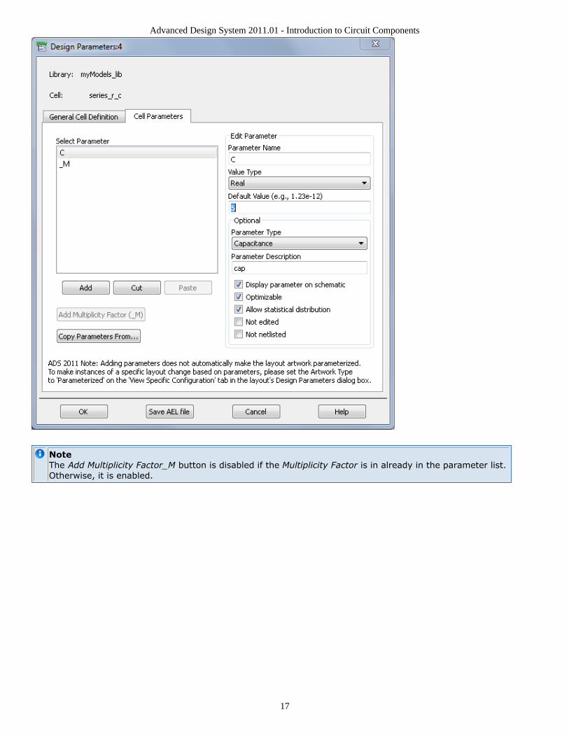
Multiplicity Parameter _MThe multiplicity feature provides a way to scale components or entire sub-circuitscontaining many components and sub-circuits. Given a component with a multiplicityvalue M , the simulator treats this component as if there were M such components allconnected in parallel. Sub-circuits within sub-circuits will be appropriately scaled.
The _M parameter is available at the component level as shown here. (For componentsthat don't explicitly have a Multiplicity parameter, the same functionality can be achievedby placing the component in a sub-circuit and using the sub-circuit's Multiplicityparameter, as described next.)
For sub-circuits, the parameter is enabled by selecting File > Design Parameters fromthe Schematic window. In the dialog box, select the Parameters tab. To add theMultiplicity parameter, choose Add Multiplicity Factor_M.
Advanced Design System 2011.01 - Introduction to Circuit Components
17
NoteThe Add Multiplicity Factor_M button is disabled if the Multiplicity Factor is in already in the parameter list.Otherwise, it is enabled.

Advanced Design System 2011.01 - Introduction to Circuit Components
18
Series IV or MDS Product Migration ComponentsOlder Series IV or MDS components can still be placed in ADS designs. While they are notaccessible from the component library, they can be placed in a Schematic window byentering the exact component name in the Component History field above the designarea, pressing Enter, and moving the cursor into the design area. Documentation is notprovided for these components.
Series IV Components
GAINPULSE_TRAIN
Spectral Sources
GMSK_SOURCEPIQPSK_SOURCEQAM16_SOURCEQPSK_SOURCE
Wideband Modems
AM_DemodBroadAM_ModBroadFM_DemodBroadFM_ModBroadIQ_ModBroadQAM_ModBroadQPSK_ModBroadPM_DemodBroadPM_ModBroad
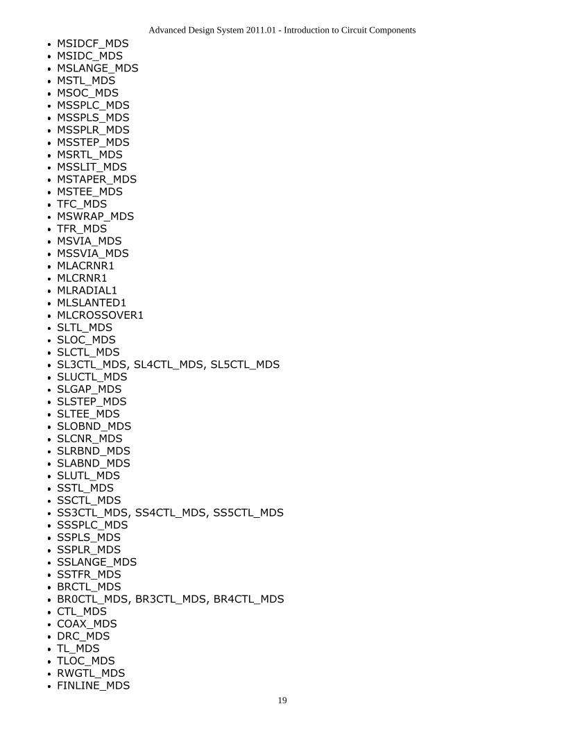
MDS Components
CPWTL_MDSGCPWTL_MDSCPWCTL_MDSACPW_MDSACPWTL_MDSCPWTLFG_MDSMSACTL_MDSMS3CTL_MDS, MS4CTL_MDS, MS5CTL_MDSMSABND_MDSMSBEND_MDSMSOBND_MDSMSCRNR_MDSMSTRL2_MDSMSCTL_MDSMSCROSS_MDSMSRBND_MDSMSGAP_MDSMSAGAP_MDS
Advanced Design System 2011.01 - Introduction to Circuit Components
19
MSIDCF_MDSMSIDC_MDSMSLANGE_MDSMSTL_MDSMSOC_MDSMSSPLC_MDSMSSPLS_MDSMSSPLR_MDSMSSTEP_MDSMSRTL_MDSMSSLIT_MDSMSTAPER_MDSMSTEE_MDSTFC_MDSMSWRAP_MDSTFR_MDSMSVIA_MDSMSSVIA_MDSMLACRNR1MLCRNR1MLRADIAL1MLSLANTED1MLCROSSOVER1SLTL_MDSSLOC_MDSSLCTL_MDSSL3CTL_MDS, SL4CTL_MDS, SL5CTL_MDSSLUCTL_MDSSLGAP_MDSSLSTEP_MDSSLTEE_MDSSLOBND_MDSSLCNR_MDSSLRBND_MDSSLABND_MDSSLUTL_MDSSSTL_MDSSSCTL_MDSSS3CTL_MDS, SS4CTL_MDS, SS5CTL_MDSSSSPLC_MDSSSPLS_MDSSSPLR_MDSSSLANGE_MDSSSTFR_MDSBRCTL_MDSBR0CTL_MDS, BR3CTL_MDS, BR4CTL_MDSCTL_MDSCOAX_MDSDRC_MDSTL_MDSTLOC_MDSRWGTL_MDSFINLINE_MDS

Advanced Design System 2011.01 - Introduction to Circuit Components
20
ETAPER_MDSSLOTTL_MDSRIBBONG_MDSRIBBONS_MDSWIREG_MDSWIRES_MDS

Advanced Design System 2011.01 - Introduction to Circuit Components
21
Term (Port Impedance for S-parameters)
Symbol
Parameters
Name Description Units Default
Num Port number Integer 1
Z Reference impedance, use 1+j*0 for complex Ohm 50
Noise Enable/disable port thermal noise: yes, no (for AC or harmonic balance analysis only;not for S-parameter analysis)
None yes
Vdc Open circuit DC voltage None
Temp Temperature °C None
Notes/Equations
Term can be used in all simulations. For S-parameter simulations it is used to define1.the impedance and location of the ports. When not in use, it is treated as animpedance with the value R + JX. The reactance is ignored for dc simulations.

Advanced Design System 2011.01 - Introduction to Circuit Components
22
Data File ComponentsDataAccessComponent (Data Access Component) (ccsim)De_Embed and De_EmbedSnP (2-Port to 12-Port De-Embed Data File) (ccsim)Deembed1 (1-Port De-Embed Data File) (ccsim)Deembed2 (2-Port De-Embed File) (ccsim)Deembed4 (4-Port De-Embed Data File) (ccsim)Deembed6 (6-Port De-Embed Data File) (ccsim)Deembed8 (8-Port De-Embed Data File) (ccsim)Deembed12 (12-Port De-Embed Data File) (ccsim)NetlistInclude (Netlist File Include Component) (ccsim)S1P (1-Port S-parameter File) (ccsim)S2P (2-Port S-parameter File) (ccsim)S2P Conn (2-Port S-parameter File connector artwork) (ccsim)S2PMDIF (Multi-Dimensional 2-Port S-parameter File) (ccsim)S2P Pad3 (2-Port S-parameter File pad artwork) (ccsim)S2P Spac (2-Port S-parameter File) (ccsim)S3P (3-Port S-parameter File) (ccsim)S4P (4-Port S-parameter File) (ccsim)S5P to S9P (5-Port to 9-Port S-parameter File) (ccsim)S10P to S20P (10-Port to 20-Port S-parameter File) (ccsim)S21P to S99P (21-Port to 99-Port S-parameter File) (ccsim)SnP component (n99) (ccsim)SnP Diff component (ccsim)VAR (Variables and Equations Component) (ccsim)W_Element (Multi-Conductor Transmission Lines) (ccsim)XnP Components (X1P - X10P) (ccsim)
Advanced Design System 2011.01 - Introduction to Circuit Components
23
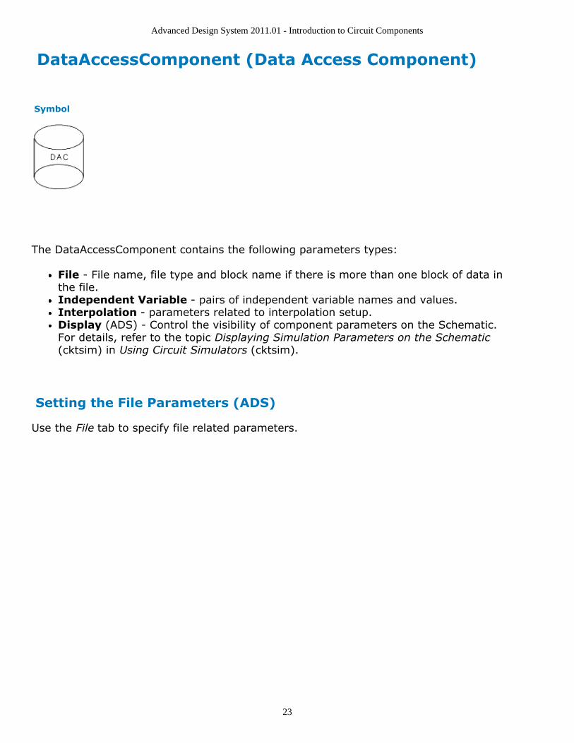
DataAccessComponent (Data Access Component)
Symbol
The DataAccessComponent contains the following parameters types:
File - File name, file type and block name if there is more than one block of data inthe file.Independent Variable - pairs of independent variable names and values.Interpolation - parameters related to interpolation setup.Display (ADS) - Control the visibility of component parameters on the Schematic.For details, refer to the topic Displaying Simulation Parameters on the Schematic(cktsim) in Using Circuit Simulators (cktsim).
Setting the File Parameters (ADS)
Use the File tab to specify file related parameters.

Advanced Design System 2011.01 - Introduction to Circuit Components
24
Parameters
Name Description Units Default
FileName
File name None None
FileType
Discrete, model MDIF, S2PMDIF, Dataset, Touchstone, CITIfile, P2D MDIF, S2DMDIF, IMT MDIF, GCOMP MDIF, FIR MDIF, SPW, TIM MDIF, SPE MDIF, SDF, GenericMDIF, COD MDIF, LAS MDIF, Value
None Discrete
BlockName
Block name None None
File Name
The file name can be defined in either Data filename entry mode or File Based entrymode. When Data filename entry mode is selected, file name can be given as a stringwhich represents explicit file name or assigned through a variable as @variable_name .

Advanced Design System 2011.01 - Introduction to Circuit Components
25
Select Edit to display the file or modify its contents.Select Copy Template to copy a data file of a specific format for use as a template.Select Data files list to select a data file in the current workspace.
File Type
Provides a drop down list of available file types.
Block
If you do not specify a block name, the block of data contained in the dataset file is used.The Block parameter is required when the generic MDIF file has multiple blocks.Here is an example of a generic MDIF file with multiple blocks. A DAC which referencesthis file should have Block set to "VB" or "IQ". Note that the outer independent variablesVc1 and Vb1 will only apply to block VB; they will have no relation to block IQ.VAR Vc1(1) = 0.2
VAR Vb1(1) = 0.3
BEGIN VB
% Index_a(1) Vbase(1)
0 0.3
1 0.4

Advanced Design System 2011.01 - Introduction to Circuit Components
26
END
BEGIN IQ
% Index_b(1) Ib_A(1) Ic_A(1)
0 1.0E-005 0.002
1 2.0E-005 0.003
END
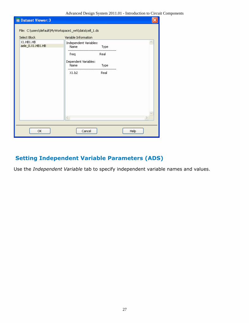
DataSet Viewer
The View Dataset button is only enabled when an explicit file name is given and the filetype is dataset . If a file name is given with a relative path, <cur_wrk>/data/ is pre-appended to the file name by ADS. Click View Dataset to open a new window displayingthe data blocks contained in the file and information about the independent anddependent variables in the selected block. ADS automatically sets up Block and iVar*(independent variable names) if a block is selected and OK is chosen in the datasetviewing window.
When no data block is specified, the Dataset Viewer defaults to the first data block in thefile. If there is more than one block of data, you can click another block to select it andview its variable information.
Advanced Design System 2011.01 - Introduction to Circuit Components
27
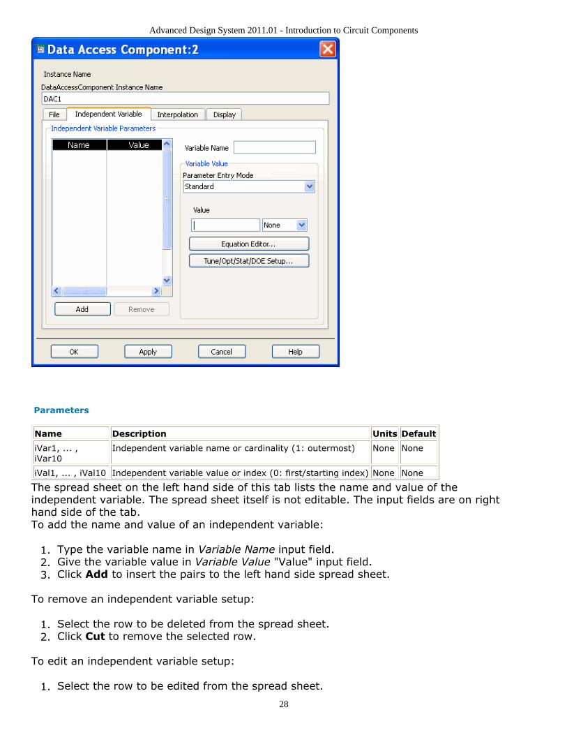
Setting Independent Variable Parameters (ADS)
Use the Independent Variable tab to specify independent variable names and values.
Advanced Design System 2011.01 - Introduction to Circuit Components
28
Parameters
Name Description Units Default
iVar1, ... ,iVar10
Independent variable name or cardinality (1: outermost) None None
iVal1, ... , iVal10 Independent variable value or index (0: first/starting index) None None
The spread sheet on the left hand side of this tab lists the name and value of theindependent variable. The spread sheet itself is not editable. The input fields are on righthand side of the tab.To add the name and value of an independent variable:
Type the variable name in Variable Name input field.1.Give the variable value in Variable Value "Value" input field.2.Click Add to insert the pairs to the left hand side spread sheet.3.
To remove an independent variable setup:
Select the row to be deleted from the spread sheet.1.Click Cut to remove the selected row.2.
To edit an independent variable setup:
Select the row to be edited from the spread sheet.1.
Advanced Design System 2011.01 - Introduction to Circuit Components
29
Modify the name or value on the right hand side input fields.2.
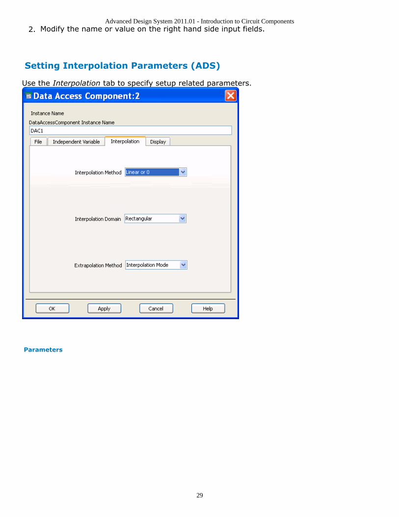
Setting Interpolation Parameters (ADS)
Use the Interpolation tab to specify setup related parameters.
Parameters

Advanced Design System 2011.01 - Introduction to Circuit Components
30
Name Description Units Default
InterpolationMethod(InterpMode)
Interpolation mode: Index Lookup Specifies that iVal n represents theinteger indices (beginning with 0) of the independent variables in thedata file. Real iVal values are truncated first for index lookup. Note Ifyou use the Index Lookup interpolation mode, you can access and/orinterpolate the "indices" of the independent variable in the file. In thiscontext the first data row of the file will have an index of 0, the secondrow will have an index of 1 and so on.Value Lookup For real/integer independent variable, accesses thepoint in the data file closest to the specified value. If midway, theaverage of the bracketing points is used.Ceiling Value Lookup For a real independent variable, accesses thenearest point in the data file not less than the specified value.Floor Value Lookup For a real independent variable, accesses thenearest point in the data file not greater than the specified value.Linear, Cubic, Cubic Spline Specifies the interpolation mode in eachdimension (except for splines, where only the innermost variable isspline-interpolated).Value This is provided if the interpolation mode is variable orunknown, for example, as a passed parameter of a subnetwork. Theresulting value should be a string (or integer) from the following set:
{"linear"(0), "spline"(1), "cubic"(2), "index_lookup"(3),
"value_lookup"(4), "ceiling_value_lookup"(5), "floor_value_lookup"(6)}
None Index Lookupor 3
InterpolationDomain(InterpDom)
Interpolation domain: Rectangular Interpolates real and imaginaryparts separately; recommended for emittances. Polar (arcinterpolation) Interpolates magnitude and angle separately;recommended for S-parameters. DB Interpolates in dB and angleformat.Value This is provided if the interpolation domain is a variable orunknown; for example as a passed parameter of a subnetwork. Theresulting value should be a string (or integer) from the following set:
{"ri" (0), "ma" (1), "db" (3) }
None Rectangular
ExtrapolationMethod(ExtrapMode)
Extrapolation mode: Interpolation Mode: when extrapolation occurs,the interpolation mode specified by InterpMode is used forextrapolation.Constant Extrapolation: when extrapolation occurs, no interpolationis performed. The value of the nearest data point is returned.An extrapolation warning is issued when an extrapolation occurs onfreq in an S-parameter simulation. For all other analysis types, statuslevel in the analysis controller must be set to 3 or higher to seeextrapolation warnings.
None InterpretationMode
Notes/Equations
This component can be used to extract/interpolate multidimensional dependent1.variables as a function of up to 10 independent variables. By setting the DAC Fileparameter to the desired filename, and setting the parameter of the component ofinterest to point to the DAC (by Instance ID), the data in the specified file can beaccessed. (Refer to Example 1)
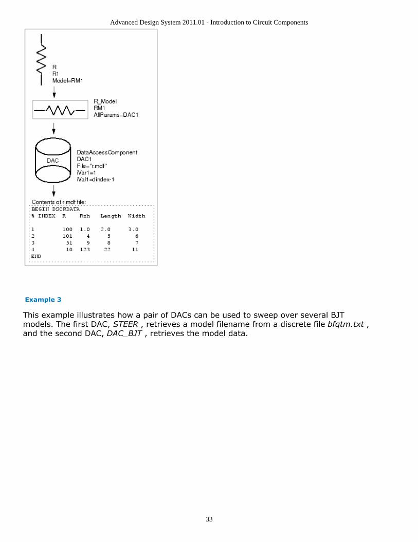
You can quickly set all parameters (with matching names) of a device model bysetting the model's AllParams parameter to the DAC's Instance ID, which inturn, references the data file. Parameter names in a data file that are not devicemodel parameters are ignored. A device model parameter value that is explicitly

Advanced Design System 2011.01 - Introduction to Circuit Components
31
specified will override the value set by an AllParams association. (Refer toExample 2)You can also sweep over several BJT models using two DAC components. (Referto Example 3)S-parameter data can be read directly from a Touchstone file using a DAC.(Refer to Example 4).Discrete data can be read directly from a Discrete data type file using a DAC inan ADS Ptolemy simulation. (Refer to Example 5).Multi-dimensional data can be read directly from a Generalized Multi-dimensional data type file using a DAC in an ADS Ptolemy simulation. (Refer toExample 6).Ptolemy simulation examples using DAC are located in the Controllers_wrk; toaccess the example from the ADS Main window, click on File > Open >Example > PtolemyDocExamples > Controllers_wrk , then open theRead_DAC_DSCR and Read_DAC_MDIF designs.
For a complex dependent variable, the two parts (real/imag, mag/degree, or2.dB/degree) are interpolated separately. For arc-like data (for example S-parametersvs. frequency), it may be more appropriate to interpolate in the mag/degree domain.This component is actually a special subnetwork whose expressions can be used3.outside. In particular, one of these expressions is _TREE (the multi-dimensionaltable). The following example shows using this expression with the get_max_points{{}} function.Example: get_max_points(DAC1._TREE, "freq")where:DAC1._TREE represents the Instance ID of the DAC{{"freq" }} represents the name of the independent variableIt returns the maximum # of points (over all sweeps of that variable) of theindependent variable (for discrete files with implicit row #, use 1 for the secondargument)
The Type parameter specifies the format of the disk file, which includes Touchstone,4.CITIfile, several MDIF types, SPW and binary datasets (possibly from a previoussimulation or via instrument server).The files displayed in the Browser represent all files found based on the search pathsspecified by the DATA_FILES configuration variable.For information on data file formats, refer to Working with Data Files (cktsim).The Block name specifies which table to use when the file contains two or more5.multidimensional tables, (e.g., "ACDATA", "NDATA" in an MDIF file, "HB1.HB","HB1.HB_NOISE" in a harmonic balance analysis dataset). A unique prefix issufficient; it can also be the sequence number (starting with 1) of the table, forexample, 1 for an "ACDATA" table and 2 for "NDATA". Note that the " at " symbol(@) should be used to suppress quotes when using a variable to identify a table asthe independent variable for making DAC parameter assignments.Each iVar is either the name of an independent variable in the file (e.g., Vgs) or is an6.integer representing the cardinality or nesting order of the independent variable (1being outermost). A cardinal value must be used when an independent variable isimplicit; for example, row index in discrete files is the innermost independentvariable. Note that @ must be used to suppress quotes when using a variable, for
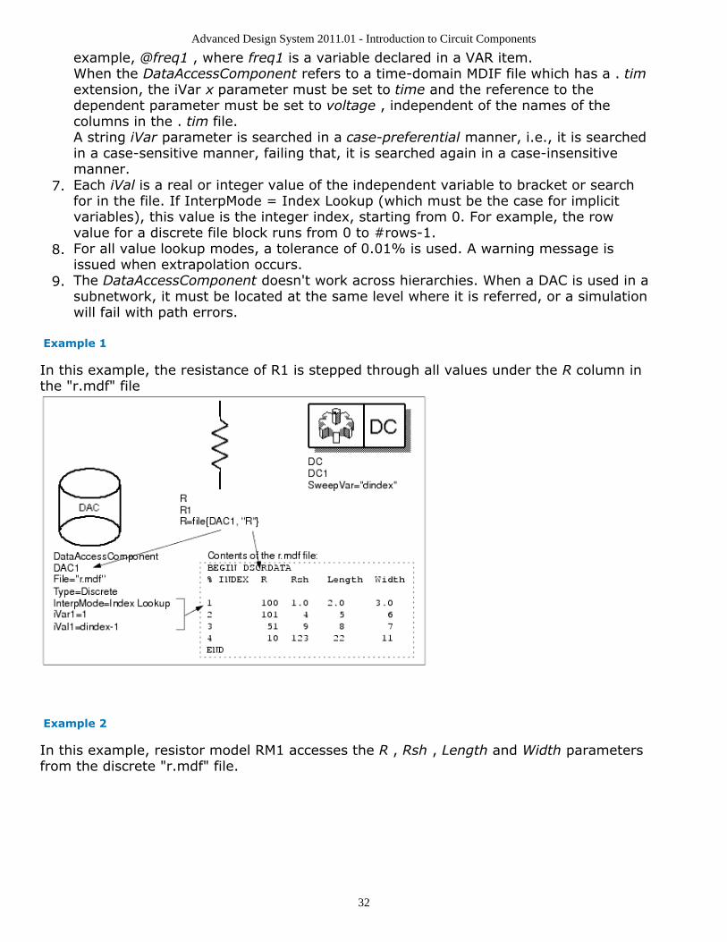
Advanced Design System 2011.01 - Introduction to Circuit Components
32
example, @freq1 , where freq1 is a variable declared in a VAR item.When the DataAccessComponent refers to a time-domain MDIF file which has a . timextension, the iVar x parameter must be set to time and the reference to thedependent parameter must be set to voltage , independent of the names of thecolumns in the . tim file.A string iVar parameter is searched in a case-preferential manner, i.e., it is searchedin a case-sensitive manner, failing that, it is searched again in a case-insensitivemanner.Each iVal is a real or integer value of the independent variable to bracket or search7.for in the file. If InterpMode = Index Lookup (which must be the case for implicitvariables), this value is the integer index, starting from 0. For example, the rowvalue for a discrete file block runs from 0 to #rows-1.For all value lookup modes, a tolerance of 0.01% is used. A warning message is8.issued when extrapolation occurs.The DataAccessComponent doesn't work across hierarchies. When a DAC is used in a9.subnetwork, it must be located at the same level where it is referred, or a simulationwill fail with path errors.
Example 1
In this example, the resistance of R1 is stepped through all values under the R column inthe "r.mdf" file
Example 2
In this example, resistor model RM1 accesses the R , Rsh , Length and Width parametersfrom the discrete "r.mdf" file.
Advanced Design System 2011.01 - Introduction to Circuit Components
33
Example 3
This example illustrates how a pair of DACs can be used to sweep over several BJTmodels. The first DAC, STEER , retrieves a model filename from a discrete file bfqtm.txt ,and the second DAC, DAC_BJT , retrieves the model data.

Advanced Design System 2011.01 - Introduction to Circuit Components
34
NoteAn assignment of the type: R1=file{DAC1, ''Rnom''}, is equivalent to the expressionR1=dep_data(DAC1._DAC, '' Rnom '').
Example 4
This example illustrates reading S-parameter data from a Touchstone file using theDataAccessComponent.

Advanced Design System 2011.01 - Introduction to Circuit Components
35
Example 5
This example illustrates reading discrete data from the file data_DSCR.mdf using theDataAccessComponent (DAC) in an ADS Ptolemy design.
Example 6

Advanced Design System 2011.01 - Introduction to Circuit Components
36
This example illustrates reading generalized multi-dimensional data from the filedata_MDIF.mdf using the DataAccessComponent (DAC) in an ADS Ptolemy design.
Advanced Design System 2011.01 - Introduction to Circuit Components
37
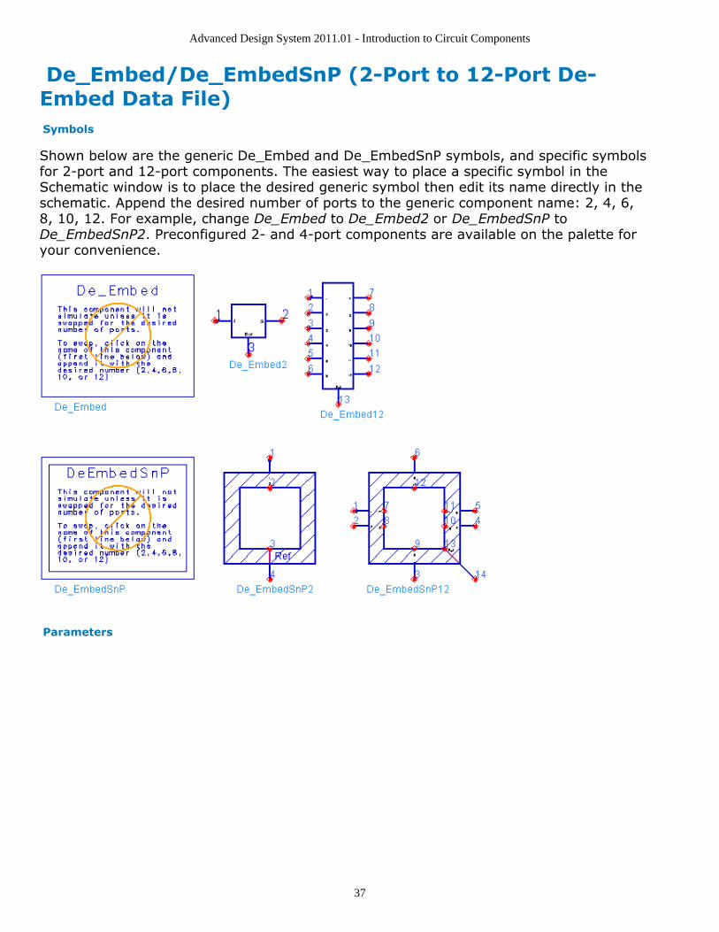
De_Embed/De_EmbedSnP (2-Port to 12-Port De-Embed Data File) Symbols
Shown below are the generic De_Embed and De_EmbedSnP symbols, and specific symbolsfor 2-port and 12-port components. The easiest way to place a specific symbol in theSchematic window is to place the desired generic symbol then edit its name directly in theschematic. Append the desired number of ports to the generic component name: 2, 4, 6,8, 10, 12. For example, change De_Embed to De_Embed2 or De_EmbedSnP toDe_EmbedSnP2. Preconfigured 2- and 4-port components are available on the palette foryour convenience.
Parameters

Advanced Design System 2011.01 - Introduction to Circuit Components
38
Setup DialogName
ParameterName
Description Units Default
File Name File Name of the data file containing S-, G-, H-, Y-, orZ-parameters for this component; the fileextension and directory path are optional. Defaultdirectory is <wrk>/data where <wrk> is yourcurrent workspace directory.
None None
File Type Type File type: Touchstone, Dataset, CITIfile, Value None Touchstone
Block Name Block (for Type=Dataset) Name of S-parameter datablock
None None
InterpolationMethod
InterpMode Interpolation method: Linear or 0, Cubic Spline or1, Cubic or 2, Value Lookup or 4, Ceiling ValueLookup or 5, Floor Value Lookup or 6
None Linear or 0
InterpolationDomain
InterpDom Interpolation domain: Data Based, Rectangular,Polar, DB
None Data Based
ExtrapolationMethod
ExtrapMode Extrapolation method: Interpolation Mode,Constant Extrapolation
None ConstantExtrapolation
Pin-to-portmapping Type
PortMappingType Standard (1), Custom (2) None Standard
Pin-to portmapping
PortMapping[n] Integer array of fixture port mapping with respectto the reference (standard) pin arrangement;default is: 1,2,3,...
None Standard
Display Display parameter on schematic: File, Type,Block, InterpMode, InterpDom, ExtrapMode,PortMappingType, PortMapping
None File,PortMappingType
Range of Usage
The De_Embed/De_EmbedSnP components should be used within the frequency1.range of the S-, G-, H-, Y-, or Z-parameter data.The De_Embed/DeEmbedSnP components are not intended for, and should not be2.used in transient simulations.For proper de-embeding operation, the S-, G-, H-, Y-, or Z data must represent a bi-3.lateral (not necessarily reciprocal) behavior between the corresponding input andoutput ports at all simulation frequencies.
Notes
The data file, identified by the parameter File, must contain p-port data in the form of1.p×p S, Y, G, H or Z matrices. Only even numbers of ports p = 2n are allowed. In thecase of S parameters, the use of different port reference impedances for differentports is supported. Also, complex reference impedances are supported provided thatthe definition of the S parameters is consistent with that of ADS (i.e., the powerdefinition).For information on data file formats, refer to Working with Data Files (cktsim), in the2.Using Circuit Simulators (cktsim) documentation.Block is used only when Type=Dataset. Specify the name of an S-parameter data3.block if there are multiple S-parameter data blocks in a dataset file. If Block remainsblank, the first S-parameter data block in the dataset file will be used.InterpDom defines the domains in which two parts of a complex dependent variable4.are interpolated:
Rectangular: transform to (real, imag) before interpolationPolar: transform to (mag, angle) before interpolation

Advanced Design System 2011.01 - Introduction to Circuit Components
39
DB: transform to (dB, angle) before interpolationData Based: (Series IV compatibility) uses Polar for S-parameters, Rectangularfor Y- and Z-parameters
ExtrapMode specifies the extrapolation mode:5.Interpolation Mode: when extrapolation occurs, the interpolation mode specifiedby InterpMode is used for extrapolation.Constant Extrapolation: when extrapolation occurs, no interpolation isperformed; the value of the nearest data point is returned.
This component does not generate any noise.6.
Usage/Terminology
As shown at the top, there are two symbols for each number of ports p: De_Embed1.and De_EmbedSnP. De_Embed is a universal symbol with the input (the first n ports)on the left and with the output (the remaining n ports) on the right. Thisarrangement reflects the cascaded nature of the de-embeding process.De_EmbedSnP is specifically designed for the prevailing case of the embedded DUTbeing an SnP component. It enforces the cascaded connection by snapping the SnPsymbol to the inside of the De_EmbedSnP symbol.The available connection nodes include p (2n) pins and a reference pin Ref, and thus2.the total number of connection nodes is 2n + 1. The reference pin is numbered as2n + 1 in the universal symbol. The SnP type symbols have two reference nodes,namely 2n + 1 and 2n + 2, which are short-circuited internally. Node 2n + 2 isintended for external connections.The ports of the component are established by pairs of nodes with one of the first 2n3.pins as the "+" node and with the reference pin as the "-" node. The numbering ofthe ports of the De-Embed components follow that of the pin numbering: the kth portis established between the pins k and Ref.The first n ports are termed the input ports. The ports n + 1, ..., 2n are termed the4.output ports.The connection (hook-up) of the De-Embed components to the embedded DUT5.(eDUT) is described in the section Connecting De_Embed Component to eDUT.The section Fixture Pin/Port Mapping describes how to handle non-standard fixture6.data.
Embeded DUT (eDUT)
The purpose of the De_Embed components is to undo the effect of taking measurementsat some externally available ports instead of the ports of interest: the ports of DUT(Device Under Test).

Advanced Design System 2011.01 - Introduction to Circuit Components
40
As shown in the diagram above, a measurement fixture is present between the points ofactually taken measurements and DUT, and thus the measurement data is that of theembedded DUT (eDUT). The underlying assumption here is that the pins of eDUTcorrespond to the same numbered pins of DUT (the ports are established with respect tothe Ref node and numbered consistently with the pins).
Connecting De_Embed Component to eDUT
There are two ways to connect the De_Embed component to eDUT. The first one isdescribed here and the other in the next section. The first of the two connections followsan intuitive placement and wiring as shown in the following figure. The shape of theDe_EmbedSnP components enforces the same pin-to-pin connection as for the universalcomponent shown. The electrical behavior of eDUT is described by n-port parameters ofthe emebeded DUT, i.e., of DUT plus the fixture. The electrical behavior of the De_Embedcomponent is described by 2n-port parameters of the fixture.
The underlying motivation in this connection is for the input pins of the De_Embedcomponent to represent the same numbered pins of eDUT, and therefore the samenumbered pins of DUT. Note that an additional requirement in this hook-up is that theoutput (n+k)th pin of the De_Embed component is to be connected to the kth pin of eDUT.Examples of actual schematic connections are as follows.

Advanced Design System 2011.01 - Introduction to Circuit Components
41
By combining the diagrams of Embeded DUT and of the above connection of theDe_Embed component to eDUT we have the following reference diagram.
Reference De-embeding Diagram
This diagram shows a reference connection of the fixture to DUT, resulting in a standardcascade connection of the De_Embed component and the fixture. Here, the term standardcascade refers to the fact that the input of one is connected to the output of the other.The cascade connection is the foundation of the de-embeding process as it is to providetransparent connections from the inputs of the De_Embed component to thecorresponding inputs of DUT.
The simulation results of cascading the De_Embed component and the fixture can beaffected by port ordering of the fixture. To facilitate the desired transparency of theDe_Embed/fixture cascade the 2n-port data of the fixture (used by the De_Embedcomponent) must have the port numbering consistent with the pin numbering of thefixture shown above. If it is not the case, please see the section Fixture Pin/Port Mapping.
Alternative Connection at the Output Side
If you want to place the De_Embed component on the right-hand side of eDUT, one way isto follow the mirror images of the preceding diagrams. However, you may prefer to usethe following, alternative connection.
This alternative hook-up, shown in the Alternative Reference De-embeding Diagram, alsouses the standard cascade connection of the fixture and the De_Embed component, just inthe opposite order. Here the output of the fixture is connected to the input of theDe_Embed component.
In this hook-up the port associated with the (n+k)th pin of the De_Embed component

Advanced Design System 2011.01 - Introduction to Circuit Components
42
represents the kth port of DUT.
Alternative Reference De-embeding Diagram
Again, to facilitate the desired transparency of the fixture/De_Embed cascade the 2n-portdata of the fixture (used by the De_Embed component) must have the port numberingconsistent with the pin numbering of the fixture shown above. If it is not the case, pleaserefer to the section Fixture Pin/Port Mapping.
Fixture Pin/Port Mapping
The port mapping feature of the De_Embed component helps to accommodate the caseswhere the fixture 2n-port data (which is the input data for the De_Embed component)does not conform to the standard cascade configurations shown either in the ReferenceDe-embeding Diagram or the Alternative Reference De-embeding Diagram, respectively. Ifthe fixture measurement setup is such that the port ordering is not consistent with thereference pin ordering then you can set Pin-to-port mapping Type to Custom and enterthe actual port numbers for each of the 2n pins.
For example, for the following fixture measurement setup
the corresponding entries for Pin-to-port mapping in the UI are as follows.

Advanced Design System 2011.01 - Introduction to Circuit Components
43
Duplicate entries are invalid and the entered port numbers must be between 1 and 2n.
Multiple Fixtures and Half-Fixtures
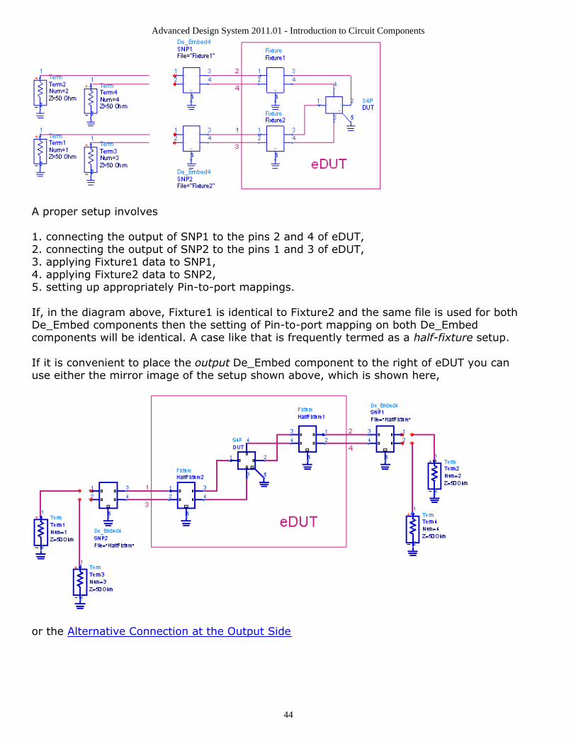
Depending on whether there exist couplings or not, the entire fixture may be split into twoor more fixtures. Instead of combining the individual fixture data into one 2n×2n matrix,two or more De_Embed components may be used. Then the universal symbols must beused.
Note that the ports of DUT are split accordingly and thus the reference numbering of DUTpins for individual fixtures is no longer applicable. For example, one fixture may beconnected to pins 1 and 3 of DUT, and another to pins 2 and 4, as shown in the followingschematic.
Advanced Design System 2011.01 - Introduction to Circuit Components
44
A proper setup involves
1. connecting the output of SNP1 to the pins 2 and 4 of eDUT,2. connecting the output of SNP2 to the pins 1 and 3 of eDUT,3. applying Fixture1 data to SNP1,4. applying Fixture2 data to SNP2,5. setting up appropriately Pin-to-port mappings.
If, in the diagram above, Fixture1 is identical to Fixture2 and the same file is used for bothDe_Embed components then the setting of Pin-to-port mapping on both De_Embedcomponents will be identical. A case like that is frequently termed as a half-fixture setup.
If it is convenient to place the output De_Embed component to the right of eDUT you canuse either the mirror image of the setup shown above, which is shown here,
or the Alternative Connection at the Output Side
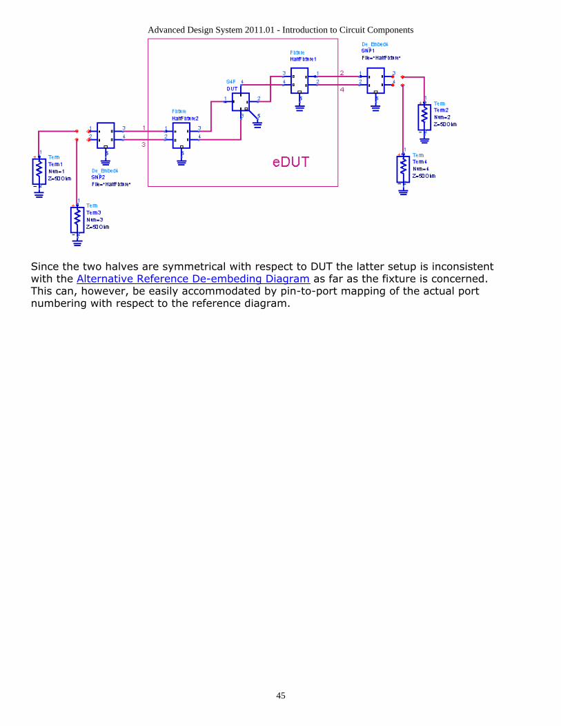
Advanced Design System 2011.01 - Introduction to Circuit Components
45
Since the two halves are symmetrical with respect to DUT the latter setup is inconsistentwith the Alternative Reference De-embeding Diagram as far as the fixture is concerned.This can, however, be easily accommodated by pin-to-port mapping of the actual portnumbering with respect to the reference diagram.

Advanced Design System 2011.01 - Introduction to Circuit Components
46
Deembed1 (1-Port De-Embed Data File)
Symbol
Parameters
Name Description Units Default
File Name Name of data file containing 1-port S-, Y-, or Z-parameters for thiscomponent. The file extension and directory path are optional.Default extension is .s1p and the default directory is <wrk>/datawhere <wrk> is your current workspace directory.
None None
File Type File type: Touchstone, Dataset, CITIfile, Value None Touchstone
Block Name (for Type=Dataset) Name of S-parameter data block None None
InterpolationMethod (orInterpMode)
Interpolation method: Linear or 0, Cubic Spline or 1, Cubic or 2,Floor Value Lookup or 4, Ceiling Value Lookup or 5, Floor ValueLookup or 6
None Linear or 0
InterpolationDomain (orInterpDom)
Interpolation domain: Data Based, Rectangular, Polar, DB None Data Based
ExtrapolationMethod (orExtrapMode)
Extrapolation method: Interpolation Mode, Constant Extrapolation None ConstantExtrapolation
Temp Physical temperature °C 27.0
Display Display parameter on schematic: File, Type, Block, InterpMode,InterpDom, ExtrapMode, Temp, UseLogFreq
None File
Range of Usage
Within the frequency range of the S-, Y-, or Z-parameter file
Notes/Equations
For information on data file formats, refer to Working with Data Files (cktsim).1.One of the Deembed1 data file applications is to negate the 1-port subcircuit by using2.this data file.In the following example, the BJT emitter's parasitics leads are de-embedded to3.obtain just the chip BJT. This ideal short and open behavior is not guaranteed if thedeembed circuit has one or more frequency bands where a stop behavior is observed.

Advanced Design System 2011.01 - Introduction to Circuit Components
47
Block is used only when Type=Dataset. Specify the name of an S-parameter data4.block when there are multiple S-parameter data blocks in a dataset file. If Blockremains blank, the first S-parameter data block in the dataset file will be used.InterpDom defines the domains in that the two parts of a complex dependent5.variable are interpolated.Rectangular: transform to (real, imag) before interpolationPolar: transform to (mag, angle) before interpolationDB: transform to (dB, angle) before interpolationData Based: (Series IV compatibility) uses Polar for S-parameters, Rectangular for Y-and Z-parametersExtrapMode specifies the extrapolation mode.6.Interpolation Mode: when extrapolation occurs, the interpolation mode specified byInterpMode is used for extrapolation.Constant Extrapolation: when extrapolation occurs, no interpolation is performed; thevalue of the nearest data point is returned.This component does not generate any noise.7.For time-domain analysis, the impulse response used for transient will be noncausal.8.This model should not be used for transient or circuit envelope analysis.This component has no default artwork associated with it.9.

Advanced Design System 2011.01 - Introduction to Circuit Components
48
Deembed2 (2-Port De-Embed File)
NoteThis component is obsolete, and has been replaced by the De_Embed/De_EmbedSnP (ccsim) component.
Symbol
Parameters
Name Description Units Default
File Name Name of data file containing 1-port S-, Y-, or Z-parameters for thiscomponent. The file extension and directory path are optional.Default extension is .s2p and the default directory is <wrk>/datawhere <wrk> is your current workspace directory.
None None
File Type File type: Touchstone, Dataset, CITIfile, Value None Touchstone
Block Name (for Type=Dataset) Name of S-parameter data block None None
InterpolationMethod (orInterpMode)
Interpolation method: Linear or 0, Cubic Spline or 1, Cubic or 2,Floor Value Lookup or 4, Ceiling Value Lookup or 5, Floor ValueLookup or 6
None Linear or 0
InterpolationDomain (orInterpDom)
Interpolation domain: Data Based, Rectangular, Polar, DB None Data Based
ExtrapolationMethod (orExtrapMode)
Extrapolation method: Interpolation Mode, Constant Extrapolation None ConstantExtrapolation
Temp physical temperature °C 27.0
Display Display parameter on schematic: File, Type, Block, InterpMode,InterpDom, ExtrapMode, Temp, UseLogFreq
None File
Range of Usage
Within the frequency range of the S-, G-, H-, Y-, or Z-parameter file
Notes/Equations
For information on data file formats, refer to Working with Data Files (cktsim).1.One of the Deembed2 data file applications is to negate the 2-port subcircuit by using2.this data file.When this component is connected in series with the sub-circuit being negated, and3.
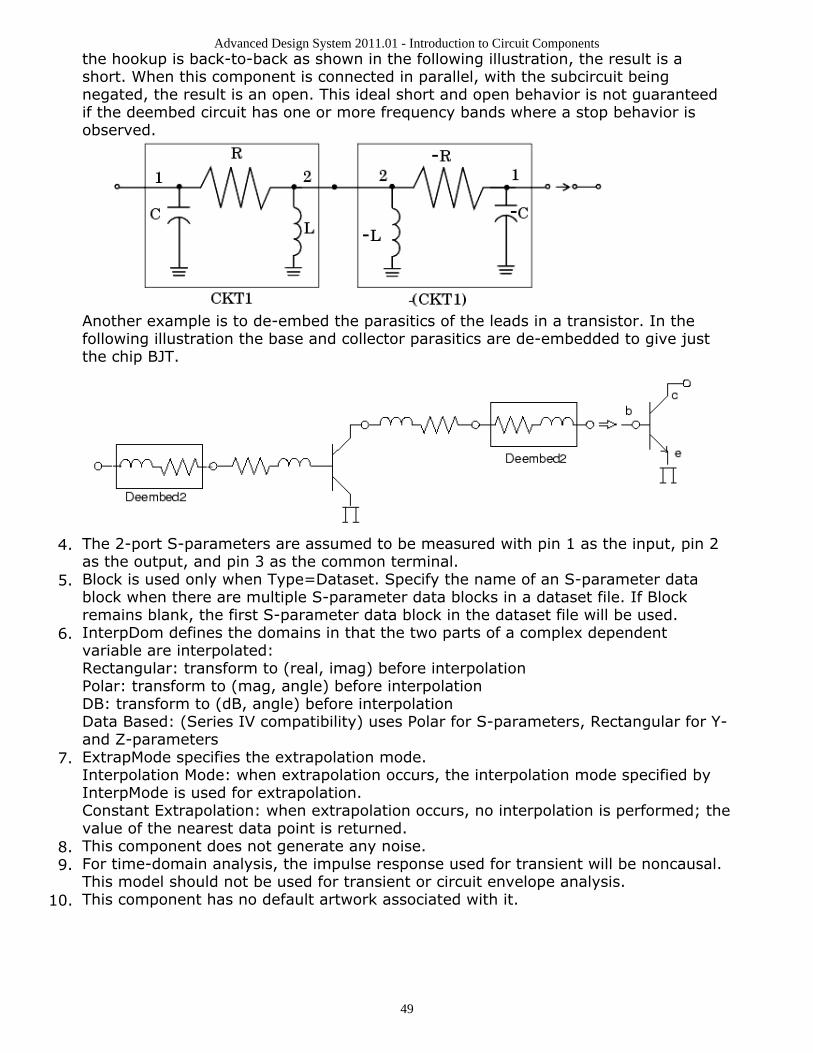
Advanced Design System 2011.01 - Introduction to Circuit Components
49
the hookup is back-to-back as shown in the following illustration, the result is ashort. When this component is connected in parallel, with the subcircuit beingnegated, the result is an open. This ideal short and open behavior is not guaranteedif the deembed circuit has one or more frequency bands where a stop behavior isobserved.
Another example is to de-embed the parasitics of the leads in a transistor. In thefollowing illustration the base and collector parasitics are de-embedded to give justthe chip BJT.
The 2-port S-parameters are assumed to be measured with pin 1 as the input, pin 24.as the output, and pin 3 as the common terminal.Block is used only when Type=Dataset. Specify the name of an S-parameter data5.block when there are multiple S-parameter data blocks in a dataset file. If Blockremains blank, the first S-parameter data block in the dataset file will be used.InterpDom defines the domains in that the two parts of a complex dependent6.variable are interpolated:Rectangular: transform to (real, imag) before interpolationPolar: transform to (mag, angle) before interpolationDB: transform to (dB, angle) before interpolationData Based: (Series IV compatibility) uses Polar for S-parameters, Rectangular for Y-and Z-parametersExtrapMode specifies the extrapolation mode.7.Interpolation Mode: when extrapolation occurs, the interpolation mode specified byInterpMode is used for extrapolation.Constant Extrapolation: when extrapolation occurs, no interpolation is performed; thevalue of the nearest data point is returned.This component does not generate any noise.8.For time-domain analysis, the impulse response used for transient will be noncausal.9.This model should not be used for transient or circuit envelope analysis.This component has no default artwork associated with it.10.

Advanced Design System 2011.01 - Introduction to Circuit Components
50
Deembed4 (4-Port De-Embed Data File)
NoteThis component is obsolete, and has been replaced by the De_Embed/De_EmbedSnP (ccsim) component.
Symbol
Parameters
Name Description Units Default
File Name Name of data file containing 1-port S-, Y-, or Z-parameters for thiscomponent. The file extension and directory path are optional.Default extension is .s4p and the default directory is <wrk>/datawhere <wrk> is your current workspace directory.
None None
File Type File type: Touchstone, Dataset, CITIfile, Value None Touchstone
Block Name (for Type=Dataset) Name of S-parameter data block None None
InterpolationMethod (orInterpMode)
Interpolation method: Linear or 0, Cubic Spline or 1, Cubic or 2,Value Lookup or 4, Ceiling Value Lookup or 5, Floor Value Lookupor 6
None Linear or 0
InterpolationDomain (orInterpDom)
Interpolation domain: Data Based, Rectangular, Polar, DB None Data Based
ExtrapolationMethod (orExtrapMode)
Extrapolation method: Interpolation Mode, Constant Extrapolation None ConstantExtrapolation
Temp Physical temperature °C 27.0
Display Display parameter on schematic: File, Type, Block, InterpMode,InterpDom, ExtrapMode, Temp
None File
Range of Usage
Within the frequency range of the S-parameter file.
Notes/Equations

Advanced Design System 2011.01 - Introduction to Circuit Components
51
For information on data file formats, refer to Working with Data Files (cktsim).1.One of the Deembed4 data file applications is to negate the 4-port subcircuit by using2.this data file.When this component is connected in series with the sub-circuit being negated, and3.the hookup is back-to-back, the result is a short. When this component is connectedin parallel, with the subcircuit being negated, the result is an open. This ideal shortand open behavior is not guaranteed if the deembed circuit has one or morefrequency bands where a stop behavior is observed.Block is used only when Type = Dataset. Specify the name of an S-parameter data4.block when there are multiple S-parameter data blocks in a dataset file. If Blockremains blank, the first S-parameter data block in the dataset file will be used.InterpDom defines the domains in that the two parts of a complex dependent5.variable are interpolated:Rectangular: transform to (real, imag) before interpolationPolar: transform to (mag, angle) before interpolationDB: transform to (dB, angle) before interpolationData Based: (Series IV compatibility) uses Polar for S-parameters, Rectangular for Y-and Z-parametersExtrapMode specifies the extrapolation mode.6.Interpolation Mode: when extrapolation occurs, the interpolation mode specified byInterpMode is used for extrapolation.Constant Extrapolation: when extrapolation occurs, no interpolation is performed; thevalue of the nearest data point is returned.This component does not generate any noise.7.For time-domain analysis, the impulse response used for transient will be noncausal.8.This model should not be used for transient or circuit envelope analysis.This component has no default artwork associated with it.9.
Advanced Design System 2011.01 - Introduction to Circuit Components
52
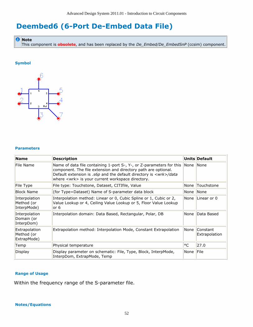
Deembed6 (6-Port De-Embed Data File)
NoteThis component is obsolete, and has been replaced by the De_Embed/De_EmbedSnP (ccsim) component.
Symbol
Parameters
Name Description Units Default
File Name Name of data file containing 1-port S-, Y-, or Z-parameters for thiscomponent. The file extension and directory path are optional.Default extension is .s6p and the default directory is <wrk>/datawhere <wrk> is your current workspace directory.
None None
File Type File type: Touchstone, Dataset, CITIfile, Value None Touchstone
Block Name (for Type=Dataset) Name of S-parameter data block None None
InterpolationMethod (orInterpMode)
Interpolation method: Linear or 0, Cubic Spline or 1, Cubic or 2,Value Lookup or 4, Ceiling Value Lookup or 5, Floor Value Lookupor 6
None Linear or 0
InterpolationDomain (orInterpDom)
Interpolation domain: Data Based, Rectangular, Polar, DB None Data Based
ExtrapolationMethod (orExtrapMode)
Extrapolation method: Interpolation Mode, Constant Extrapolation None ConstantExtrapolation
Temp Physical temperature °C 27.0
Display Display parameter on schematic: File, Type, Block, InterpMode,InterpDom, ExtrapMode, Temp
None File
Range of Usage
Within the frequency range of the S-parameter file.
Notes/Equations
Advanced Design System 2011.01 - Introduction to Circuit Components
53
For information on data file formats, refer to Working with Data Files (cktsim).1.One of the Deembed6 data file applications is to negate the 6-port subcircuit by using2.this data file.When this component is connected in series with the sub-circuit being negated, and3.the hookup is back-to-back, the result is a short. When this component is connectedin parallel, with the subcircuit being negated, the result is an open. This ideal shortand open behavior is not guaranteed if the deembed circuit has one or morefrequency bands where a stop behavior is observed.Block is used only when Type = Dataset. Specify the name of an S-parameter data4.block when there are multiple S-parameter data blocks in a dataset file. If Blockremains blank, the first S-parameter data block in the dataset file will be used.InterpDom defines the domains in that the two parts of a complex dependent5.variable are interpolated:Rectangular: transform to (real, imag) before interpolationPolar: transform to (mag, angle) before interpolationDB: transform to (dB, angle) before interpolationData Based: (Series IV compatibility) uses Polar for S-parameters, Rectangular for Y-and Z-parametersExtrapMode specifies the extrapolation mode.6.Interpolation Mode: when extrapolation occurs, the interpolation mode specified byInterpMode is used for extrapolation.Constant Extrapolation: when extrapolation occurs, no interpolation is performed; thevalue of the nearest data point is returned.This component does not generate any noise.7.For time-domain analysis, the impulse response used for transient will be noncausal.8.This model should not be used for transient or circuit envelope analysis.This component has no default artwork associated with it.9.
Advanced Design System 2011.01 - Introduction to Circuit Components
54
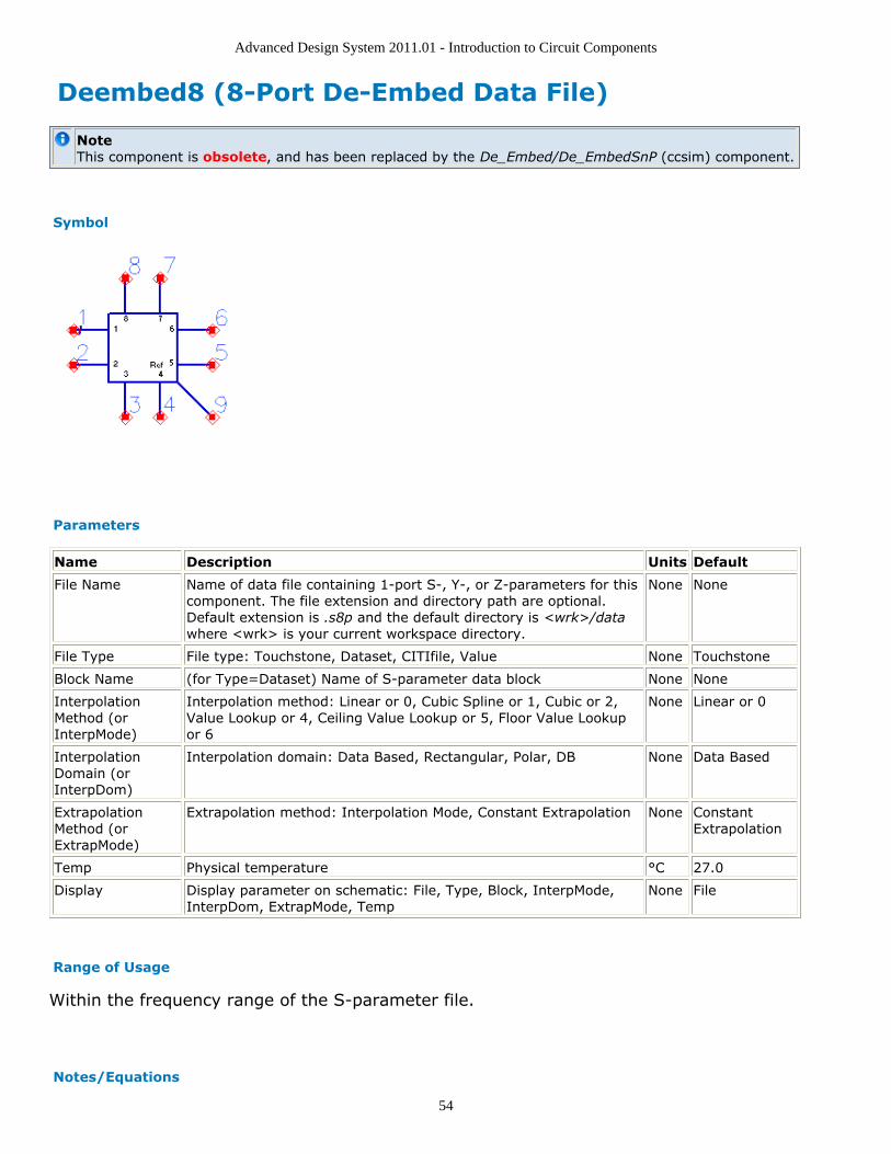
Deembed8 (8-Port De-Embed Data File)
NoteThis component is obsolete, and has been replaced by the De_Embed/De_EmbedSnP (ccsim) component.
Symbol
Parameters
Name Description Units Default
File Name Name of data file containing 1-port S-, Y-, or Z-parameters for thiscomponent. The file extension and directory path are optional.Default extension is .s8p and the default directory is <wrk>/datawhere <wrk> is your current workspace directory.
None None
File Type File type: Touchstone, Dataset, CITIfile, Value None Touchstone
Block Name (for Type=Dataset) Name of S-parameter data block None None
InterpolationMethod (orInterpMode)
Interpolation method: Linear or 0, Cubic Spline or 1, Cubic or 2,Value Lookup or 4, Ceiling Value Lookup or 5, Floor Value Lookupor 6
None Linear or 0
InterpolationDomain (orInterpDom)
Interpolation domain: Data Based, Rectangular, Polar, DB None Data Based
ExtrapolationMethod (orExtrapMode)
Extrapolation method: Interpolation Mode, Constant Extrapolation None ConstantExtrapolation
Temp Physical temperature °C 27.0
Display Display parameter on schematic: File, Type, Block, InterpMode,InterpDom, ExtrapMode, Temp
None File
Range of Usage
Within the frequency range of the S-parameter file.
Notes/Equations
Advanced Design System 2011.01 - Introduction to Circuit Components
55
For information on data file formats, refer to Working with Data Files (cktsim).1.One of the Deembed8 data file applications is to negate the 8-port subcircuit by using2.this data file.When this component is connected in series with the sub-circuit being negated, and3.the hookup is back-to-back, the result is a short. When this component is connectedin parallel, with the subcircuit being negated, the result is an open. This ideal shortand open behavior is not guaranteed if the deembed circuit has one or morefrequency bands where a stop behavior is observed.Block is used only when Type = Dataset. Specify the name of an S-parameter data4.block when there are multiple S-parameter data blocks in a dataset file. If Blockremains blank, the first S-parameter data block in the dataset file will be used.InterpDom defines the domains in that the two parts of a complex dependent5.variable are interpolated:Rectangular: transform to (real, imag) before interpolationPolar: transform to (mag, angle) before interpolationDB: transform to (dB, angle) before interpolationData Based: (Series IV compatibility) uses Polar for S-parameters, Rectangular for Y-and Z-parametersExtrapMode specifies the extrapolation mode.6.Interpolation Mode: when extrapolation occurs, the interpolation mode specified byInterpMode is used for extrapolation.Constant Extrapolation: when extrapolation occurs, no interpolation is performed; thevalue of the nearest data point is returned.This component does not generate any noise.7.For time-domain analysis, the impulse response used for transient will be noncausal.8.This model should not be used for transient or circuit envelope analysis.This component has no default artwork associated with it.9.

Advanced Design System 2011.01 - Introduction to Circuit Components
56
Deembed12 (12-Port De-Embed Data File)
NoteThis component is obsolete, and has been replaced by the De_Embed/De_EmbedSnP (ccsim) component.
Symbol
Parameters
Name Description Units Default
File Name Name of data file containing 1-port S-, Y-, or Z-parameters for thiscomponent. The file extension and directory path are optional.Default extension is .s1p and the default directory is <wrk>/datawhere <wrk> is your current workspace directory.
None None
File Type File type: Touchstone, Dataset, CITIfile, Value None Touchstone
Block Name (for Type=Dataset) Name of S-parameter data block None None
InterpolationMethod (orInterpMode)
Interpolation method: Linear or 0, Cubic Spline or 1, Cubic or 2,Value Lookup or 4, Ceiling Value Lookup or 5, Floor Value Lookupor 6
None Linear or 0
InterpolationDomain (orInterpDom)
Interpolation domain: Data Based, Rectangular, Polar, DB None Data Based
ExtrapolationMethod (orExtrapMode)
Extrapolation method: Interpolation Mode, Constant Extrapolation None ConstantExtrapolation
Temp Physical temperature °C 27.0
Display Display parameter on schematic: File, Type, Block, InterpMode,InterpDom, ExtrapMode, Temp
None File
Range of Usage
Within the frequency range of the S-parameter file.
Advanced Design System 2011.01 - Introduction to Circuit Components
57
Notes/Equations
For information on data file formats, refer to Working with Data Files (cktsim).1.One of the Deembed12 data file applications is to negate the 12-port subcircuit by2.using this data file.When this component is connected in series with the sub-circuit being negated, and3.the hookup is back-to-back, the result is a short. When this component is connectedin parallel, with the subcircuit being negated, the result is an open. This ideal shortand open behavior is not guaranteed if the deembed circuit has one or morefrequency bands where a stop behavior is observed.Block is used only when Type = Dataset. Specify the name of an S-parameter data4.block when there are multiple S-parameter data blocks in a dataset file. If Blockremains blank, the first S-parameter data block in the dataset file will be used.InterpDom defines the domains in that the two parts of a complex dependent5.variable are interpolated:Rectangular: transform to (real, imag) before interpolationPolar: transform to (mag, angle) before interpolationDB: transform to (dB, angle) before interpolationData Based: (Series IV compatibility) uses Polar for S-parameters, Rectangular for Y-and Z-parametersExtrapMode specifies the extrapolation mode.6.Interpolation Mode: when extrapolation occurs, the interpolation mode specified byInterpMode is used for extrapolation.Constant Extrapolation: when extrapolation occurs, no interpolation is performed; thevalue of the nearest data point is returned.This component does not generate any noise.7.For time-domain analysis, the impulse response used for transient will be noncausal.8.This model should not be used for transient or circuit envelope analysis.

Advanced Design System 2011.01 - Introduction to Circuit Components
58
NetlistInclude (Netlist File Include Component) Symbol
Parameters
Name Description Units Default
IncludePath Space-delimited search path for included files None None
IncludeFiles List of files to include None None
UsePreprocessor Use preprocessor: yes to use an #include directive; no to copy the full textof the file
None yes
Notes/Equations
The NetlistInclude component provides a mechanism for the ADS simulator to use an1.external file.Previous versions of built-in netlist include components (spiceInclude, geminiIncludeand idfInclude) can be placed on a schematic by typing their names into theComponent History field in the schematic window; for these components, you mustmanually enter the name of the included file. Beginning with ADS 2002,NetlistInclude is the recommended mechanism for including external files, though thedeprecated components may continue to work.The NetlistInclude component can directly read a Spectre file.2.The IncludePath parameter is a space-delimited search path that locates included3.files. Using the Browse button to select values for IncludeFiles will automatically addto IncludePath as needed. Note that, in directory names, path prefixes such as thedot (.), dot-dot (..), tilde (), and dollar sign ($) all have their usual UNIXinterpretation. The forward slash should be used as the directory delimiter, even onWindows.The IncludeFiles parameter enables you to build a list of netlist files that you want to4.include in the simulation. Use the Add button to include more than one file with asingle NetlistInclude component.Each included file may have an optional Section designator. This enables you toinclude only a portion of a file, provided that the file has been set up properly.Establishing sections within a file requires bracketing the sections using #ifdef<section> and #endif directives. As an example, this file defines a subcircuit and twosections, SelectR and SelectC:
define RCsub ( in out )
#ifdef SelectR
R:R1 in out R=50 Ohm
#endif
#ifdef SelectC
C:C1 in out C=1.0 pF
#endif
end RCsub
If this file is included with the SelectR section designated, the simulator will read thefile as:
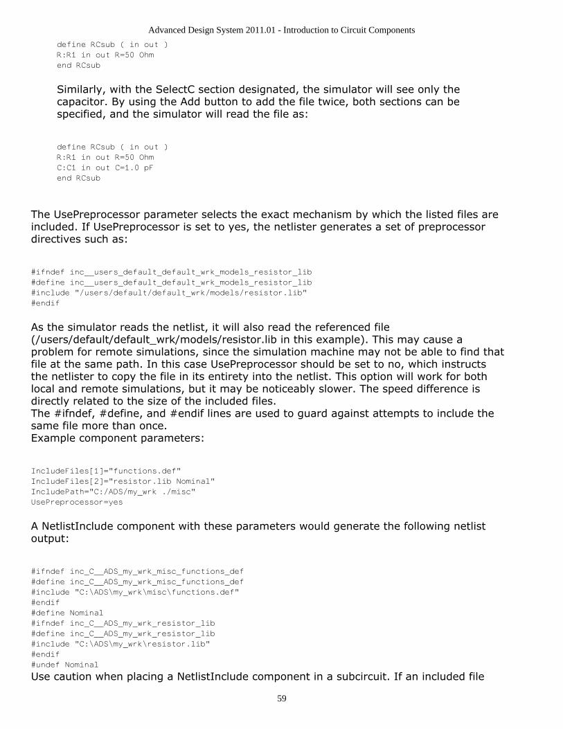
Advanced Design System 2011.01 - Introduction to Circuit Components
59
define RCsub ( in out )
R:R1 in out R=50 Ohm
end RCsub
Similarly, with the SelectC section designated, the simulator will see only thecapacitor. By using the Add button to add the file twice, both sections can bespecified, and the simulator will read the file as:
define RCsub ( in out )
R:R1 in out R=50 Ohm
C:C1 in out C=1.0 pF
end RCsub
The UsePreprocessor parameter selects the exact mechanism by which the listed files areincluded. If UsePreprocessor is set to yes, the netlister generates a set of preprocessordirectives such as:
#ifndef inc__users_default_default_wrk_models_resistor_lib
#define inc__users_default_default_wrk_models_resistor_lib
#include "/users/default/default_wrk/models/resistor.lib"
#endif
As the simulator reads the netlist, it will also read the referenced file(/users/default/default_wrk/models/resistor.lib in this example). This may cause aproblem for remote simulations, since the simulation machine may not be able to find thatfile at the same path. In this case UsePreprocessor should be set to no, which instructsthe netlister to copy the file in its entirety into the netlist. This option will work for bothlocal and remote simulations, but it may be noticeably slower. The speed difference isdirectly related to the size of the included files.The #ifndef, #define, and #endif lines are used to guard against attempts to include thesame file more than once.Example component parameters:
IncludeFiles[1]="functions.def"
IncludeFiles[2]="resistor.lib Nominal"
IncludePath="C:/ADS/my_wrk ./misc"
UsePreprocessor=yes
A NetlistInclude component with these parameters would generate the following netlistoutput:
#ifndef inc_C__ADS_my_wrk_misc_functions_def
#define inc_C__ADS_my_wrk_misc_functions_def
#include "C:\ADS\my_wrk\misc\functions.def"
#endif
#define Nominal
#ifndef inc_C__ADS_my_wrk_resistor_lib
#define inc_C__ADS_my_wrk_resistor_lib
#include "C:\ADS\my_wrk\resistor.lib"
#endif
#undef Nominal
Use caution when placing a NetlistInclude component in a subcircuit. If an included file
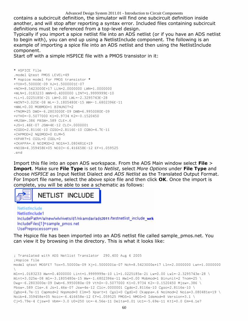
Advanced Design System 2011.01 - Introduction to Circuit Components
60
contains a subcircuit definition, the simulator will find one subcircuit definition insideanother, and will stop after reporting a syntax error. Included files containing subcircuitdefinitions must be referenced from a top-level design.Typically if you import a spice netlist file into an ADS netlist (or if you have an ADS netlistto begin with), you can end up using a NetlistInclude component. The following is anexample of importing a spice file into an ADS netlist and then using the NetlistIncludecomponent.Start off with a simple HSPICE file with a PMOS transistor in it:
* HSPICE file
.model Qtest PMOS LEVEL=49
* Hspice model for PMOS transistor *
+TOX=5.50000E-09 XJ=1.5000001E-07
+NCH=8.5423000E+17 LLN=2.0000000 LWN=1.0000000
+WLN=1.0183233 WWN=0.4000000 LINT=1.9999999E-10
+LL=1.0225185E-21 LW=0.00 LWL=-2.3295743E-28
+WINT=3.025E-08 WL=-3.1805480E-15 WW=-1.6802396E-11
+WWL=0.00 MOBMOD=1 BINUNIT=2
+TNOM=25 DWG=-6.2803000E-09 DWB=6.9950080E-09
+VTH0=-0.5077000 K1=0.9734 K2=-0.1520450
+MJSW=.386 PBSW=.589 CLE=.6
+JS=1.46E-07 JSW=4E-12 CLC=.0000001
+CGDO=2.8116E-10 CGSO=2.8116E-10 CGBO=4.7E-11
+CAPMOD=2 NQSMOD=0 ELM=5
+XPART=1 CGSL=0 CGDL=0
+CKAPPA=.6 NOIMOD=2 NOIA=3.080481E+19
+NOIB=4.359458E+05 NOIC=-6.416658E-12 EF=1.059525
.end
Import this file into an open ADS workspace. From the ADS Main window select File >Import. Make sure File Type is set to Netlist, select More Options under File Type andchoose HSPICE as Input Netlist Dialect and ADS Netlist as the Translated Output Format.For Import file name, select the above spice file and then click OK. Once the import iscomplete, you will be able to see a schematic as follows:
The Hspice file has been imported into an ADS netlist file called sample_pmos.net. Youcan view it by browsing in the directory. This is what it looks like:
; Translated with ADS Netlist Translator 290.400 Aug 6 2005
;Hspice file
model qtest MOSFET Tox=5.50000e-09 Xj=1.5000001e-07 Nch=8.5423000e+17 Lln=2.0000000 Lwn=1.0000000
\
Wln=1.0183233 Wwn=0.4000000 Lint=1.9999999e-10 Ll=1.0225185e-21 Lw=0.00 Lwl=-2.3295743e-28 \
Wint=3.025e-08 Wl=-3.1805480e-15 Ww=-1.6802396e-11 Wwl=0.00 Mobmod=1 Binunit=2 Tnom=25 \
Dwg=-6.2803000e-09 Dwb=6.9950080e-09 Vth0=-0.5077000 K1=0.9734 K2=-0.1520450 Mjsw=.386 \
Pbsw=.589 Cle=.6 Js=1.46e-07 Jsw=4e-12 Clc=.0000001 Cgdo=2.8116e-10 Cgso=2.8116e-10 \
Cgbo=4.7e-11 Capmod=2 Nqsmod=0 Elm=5 Xpart=1 Cgsl=0 Cgdl=0 Ckappa=.6 Noimod=2 Noia=3.080481e+19 \
Noib=4.359458e+05 Noic=-6.416658e-12 Ef=1.059525 PMOS=1 NMOS=0 Idsmod=8 Version=3.1 \
Cj=5.79e-4 Cjsw=0 Vbm=-3.0 U0=250 Uc=-4.56e-11 Delta=0.01 Uc1=-5.69e-11 Kt1=0.0 Em=4.1e7
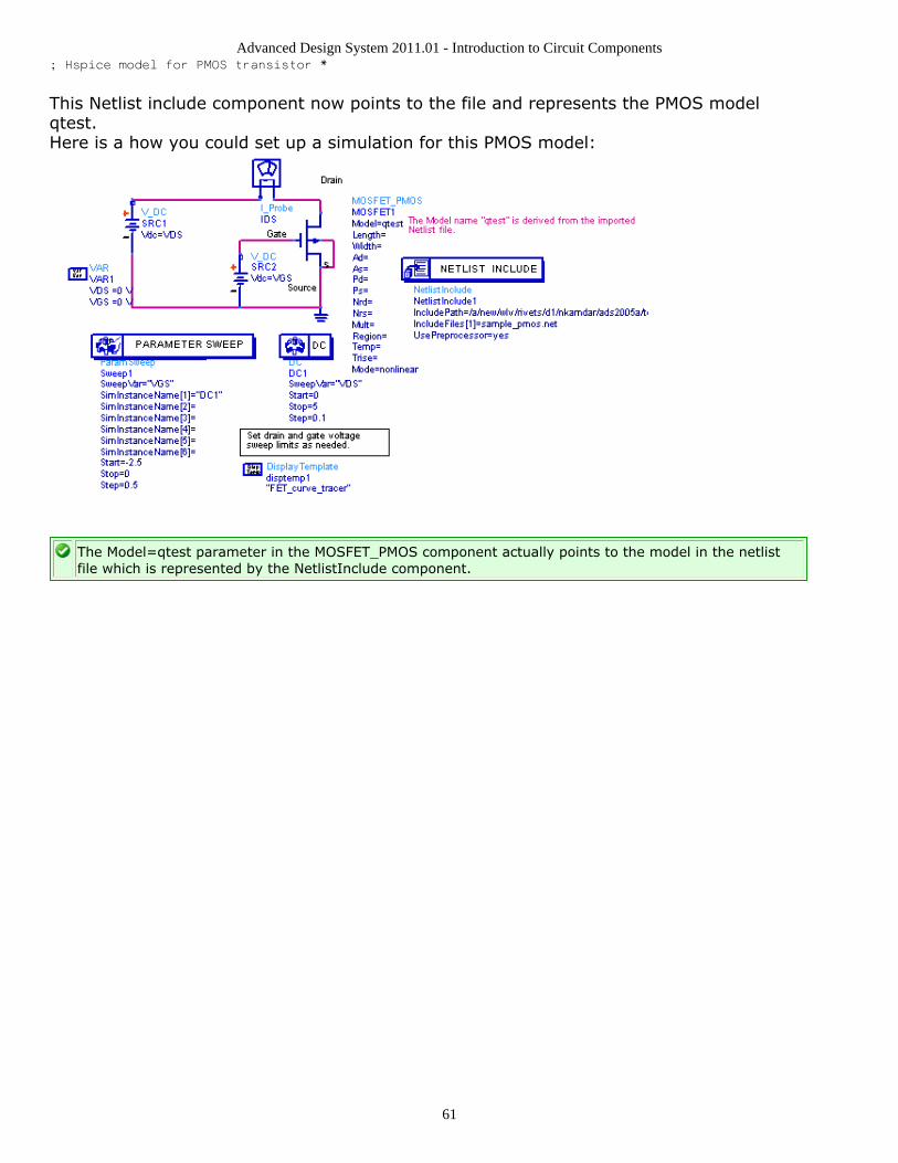
Advanced Design System 2011.01 - Introduction to Circuit Components
61
; Hspice model for PMOS transistor *
This Netlist include component now points to the file and represents the PMOS modelqtest.Here is a how you could set up a simulation for this PMOS model:
The Model=qtest parameter in the MOSFET_PMOS component actually points to the model in the netlistfile which is represented by the NetlistInclude component.

Advanced Design System 2011.01 - Introduction to Circuit Components
62
S1P (1-Port S-parameter File) Symbol
Parameters
Name Description Units Default
File Name Name of data file containing 1-port S-, Y-, or Z-parameters forthis component. The file extension and directory path areoptional. Default extension is .s1p and the default directory is<wrk>/data where <wrk> is your current workspace directory.
None None
File Type File type: Touchstone, Dataset, CITIfile None Touchstone
Block Name (for Type=Dataset) name of S-parameter data block None None
Interpolation Method(or InterpMode)
Interpolation method: Linear or 0, Cubic Spline or 1, Cubic or2, Floor Value Lookup or 4, Ceiling Value Lookup or 5, FloorValue Lookup or 6
None 0
Interpolation Domain(or InterpDom)
Interpolation domain: Data Based, Rectangular, Polar, DB None Data Based
Extrapolation Method(or ExtrapMode)
Extrapolation method: Interpolation Mode, ConstantExtrapolation
None ConstantExtrapolation
Temp Physical temperature °C 27.0
CheckPassivity Check passivity or not. Yes=check; No=do not check None no
ImpNoncausalLength Non-causal function impulse response order Integer None
ImpMode Convolution mode (value type: integer) Integer None
ImpMaxFreq Maximum frequency to which device is evaluated None
ImpDeltaFreq Sample spacing in frequency None
ImpMaxOrder Maximum impulse response order Integer None
ImpWindow Smoothing window Integer None
ImpRelTol Relative impulse response truncation factor Integer None
ImpAbsTol Absolute impulse response truncation factor Integer None
EnforcePassivity Sets passivity enforcement for S-parameters intransient/convolution simulations. If Yes is selected, passivityin this particular component is enforced. If No is selected,passivity is not enforced. If Auto is selected, the decisionfollows the setting of ImpEnforcePassivity in the Transientcontroller. This setting overwrites ImpEnforcePassivity in theTransient controller for only this component.
None Auto
Display Display parameter on schematic: File, Type, Block,InterpMode, InterpDom, extrapMode, Temp, UseLogFreq,CheckPassivity, ImpNoncausalLength, ImpMode, ImpMaxFreq,ImpDeltaFreq, ImpMaxOrder, ImpWindow, ImpRelTol,ImpAbsTol
None File
Notes/Equations
For information on data file formats, refer to Working with Data Files (cktsim).1.When an SnP component references a CITIfile, and there is more than one data block2.in the CITIfile, the simulator picks the first data block as S-parameter data. If thefirst data block is not S-parameter data, an error message might be reported by

Advanced Design System 2011.01 - Introduction to Circuit Components
63
SNPC_COMPONENT_NAME.CMP1.Block is used only when Type=Dataset. Specify the name of an S-parameter data3.block when there are multiple S-parameter data blocks in a dataset file. If Blockremains blank, the first S-parameter data block in the dataset file will be used.For the InterpMode parameter: interpolation of S-, Y-, or Z-parameters, PortZ4.reference impedance (and noise parameters for S2P) vs. simulation variable freq canbe linear, cubic spline, cubic, or lookup by actual freq value. The two parts of eachcomplex parameter (RI, MA, dBA) are interpolated independently.InterpDom defines the domains in that the two parts of a complex dependent5.variable are interpolated:Rectangular: transform to (real, imag) before interpolationPolar: transform to (mag, angle) before interpolationDB: transform to (dB, angle) before interpolationData Based: (Series IV compatibility) uses Polar for S-parameters, Rectangular for Y-and Z-parametersExtrapMode specifies the extrapolation mode. An extrapolation warning is issued6.when an extrapolation occurs on freq in an S-parameter simulation. For all otheranalysis types, status level in the analysis controller must be set to 3 or higher to seeextrapolation warnings.Interpolation Mode: when extrapolation occurs, the interpolation mode specified byInterpMode is used for extrapolation.Constant Extrapolation: when extrapolation occurs, no interpolation is performed; thevalue of the nearest data point is returned.If the component temperature Temp is less than -273°C, then the component does7.not generate any noise. If the S-parameters describe a passive device, then Tempand Twiss's theorem are used to calculate its noise performance. If the S-parametersdescribe an active device, no noise is generated.Allowed values for ImpMode are 1 (Discrete) and 2 (PWL Continuous).8.Allowed values for ImpWindow are 0 (Rectangle) and 1 (Hanning).If these values are not specified, they default to the corresponding global parametervalues specified by the transient analysis controller item.Ref pin 2 is the common terminal; it is normally grounded, but can be used in non-9.grounded mode.For time-domain analysis, the frequency-domain S-parameters are used.10.This component has no default artwork associated with it.11.

Advanced Design System 2011.01 - Introduction to Circuit Components
64
S2P (2-Port S-parameter File)
Symbol
Parameters

Advanced Design System 2011.01 - Introduction to Circuit Components
65
Name Description Units Default
File Name Name of data file containing 2-port S-, Y-, or Z-parameters forthis component. The file extension and directory path areoptional. Default extension is .s2p and the default directory is<wrk>/data where <wrk> is your current workspace directory.
None None
File Type File type: Touchstone, Dataset, CITIfile None Touchstone
Block Name (for Type=Dataset) Name of S-parameter data block None None
Interpolation Method(or InterpMode)
Interpolation method: Linear or 0, Cubic Spline or 1, Cubic or 2,Floor Value Lookup or 4, Ceiling Value Lookup or 5, Floor ValueLookup or 6
None 0
Interpolation Domain(or InterpDom)
Interpolation domain: Data Based, Rectangular, Polar, DB None Data Based
Extrapolation Method(or ExtrapMode)
Extrapolation method: Interpolation Mode, ConstantExtrapolation
None ConstantExtrapolation
Temp Physical temperature °C 27.0
CheckPassivity Check passivity or not. Yes=check; No=do not check None no
ImpNoncausalLength Non-causal function impulse response order (value type:integer)
None None
ImpMode Convolution mode (value type: integer) None None
ImpMaxFreq Maximum frequency to which device is evaluated None
ImpDeltaFreq Sample spacing in frequency None
ImpMaxOrder Maximum impulse response order (value type: integer) None None
ImpWindow Smoothing window (value type: integer) None None
ImpRelTol Relative impulse response truncation factor None None
ImpAbsTol Absolute impulse response truncation factor None None
EnforcePassivity Sets passivity enforcement for S-parameters intransient/convolution simulations. If Yes is selected, passivity inthis particular component is enforced. If No is selected,passivity is not enforced. If Auto is selected, the decision followsthe setting of ImpEnforcePassivity in the Transient controller.This setting overwrites ImpEnforcePassivity in the Transientcontroller for only this component.
None Auto
Display Display parameter on schematic: File, Type, Block, InterpMode,InterpDom, extrapMode, Temp, UseLogFreq, CheckPassivity,ImpNoncausalLength, ImpMode, ImpMaxFreq, ImpDeltaFreq,ImpMaxOrder, ImpWindow, ImpRelTol, ImpAbsTol
None File
Notes/Equations
For information on data file formats, refer to Working with Data Files (cktsim).1.The 2-port S-parameters are assumed to be measured with pin 1 as the input, pin 22.as the output, and pin 3 (Ref) as the common terminal.The Ref node (common terminal) is normally grounded; but can also be used in non-grounded mode under special circumstances. For example, an Inductor in series withref port before ground (that is, other end of inductor grounded) can be used in a BJTmodel S-parameter file to convert the amplifier to an oscillator.When an SnP component references a CITIfile, and there is more than one data block3.in the CITIfile, the simulator picks the first data block as S-parameter data. If thefirst data block is not S-parameter data, an error message might be reported bySNPC_COMPONENT_NAME.CMP1.Block is used only when Type=Dataset. Specify the name of an S-parameter data4.block when there are multiple S-parameter data blocks in a dataset file. If Block

Advanced Design System 2011.01 - Introduction to Circuit Components
66
remains blank, the first S-parameter data block in the dataset file will be used.For the InterpMode parameter: interpolation of S-, Y-, or Z-parameters, PortZ5.reference impedance (and noise parameters for S2P) vs. simulation variable freq canbe linear, cubic spline, cubic, or lookup by actual freq value. The two parts of eachcomplex parameter (RI, MA, dBA) are interpolated independently.InterpDom defines the domains in that the two parts of a complex dependent6.variable are interpolated:Rectangular: transform to (real, imag) before interpolationPolar: transform to (mag, angle) before interpolation.DB: transform to (dB, angle) before interpolationData Based: (Series IV compatibility) uses Polar for S-parameters, Rectangular for Y-and Z-parametersExtrapMode specifies the extrapolation mode. An extrapolation warning is issued7.when an extrapolation occurs on freq in an S-parameter simulation. For all otheranalysis types, status level in the analysis controller must be set to 3 or higher to seeextrapolation warnings.Interpolation Mode: when extrapolation occurs, the interpolation mode specified byInterpMode is used for extrapolation.Constant Extrapolation: when extrapolation occurs, no interpolation is performed; thevalue of the nearest data point is returned.If the component temperature Temp is less than -273°C, then the component does8.not generate any noise. If the file contains the noisy 2-port parameters (minimumnoise figure NFmin, optimum source reflection coefficient Sopt and effective noisesource resistance Rn), these parameters are used to calculate the devices noiseperformance, independent of Temp. If the S-parameters describe a passive device,then Temp and Twiss's theorem are used to calculate its noise performance. If the S-parameters describe an active device, no noise is generated.Allowed values for ImpMode are 1 (Discrete) and 2 (PWL Continuous).9.Allowed values for ImpWindow are 0 (Rectangle) and 1 (Hanning).If these values are not specified, they default to the corresponding global parametervalues specified by the transient analysis controller item.For time-domain analysis, the frequency-domain S-parameters are used.10.This component has no default artwork associated with it.11.

Advanced Design System 2011.01 - Introduction to Circuit Components
67
S2P Conn (2-Port S-parameter File; connectorartwork) Symbol
Parameters
Name Description Units Default
File Name Name of data file containing 2-port S-, Y-, or Z-parameters for thiscomponent. The file extension and directory path are optional. Defaultextension is .s2p and the default directory is <wrk>/data where <wrk> is yourcurrent workspace directory.
None None
File Type File type: Touchstone, Dataset. CITIfile, Value None Touchstone
InterpMode Interpolation mode: Linear, Cubic Spline, Cubic, Value Lookup, Ceiling ValueLookup, Floor Value Lookup, Value
None Linear
InterpDom Interpolation domain: Data Based (polar for S and rectangular for Y and Z),Rectangular, Polar, DB
None DataBased
Temp Physical temperature °C 27.0
Range of Usage
S-, G-, Y-, or Z-parameters
Notes/Equations
For information on data file formats, refer to Working with Data Files (cktsim).1.The 2-port S-parameters are assumed to be measured with pin 1 as the input, pin 22.as the output, and pin 3 (Ref) as the common terminal.The Ref node (common terminal) is normally grounded; but can also be used in non-grounded mode under special circumstances. For example, an Inductor in series withref port before ground (that is, other end of inductor grounded) can be used in a BJTmodel S-parameter file to convert the amplifier to an oscillator.When an SnP component references a CITIfile, and there is more than one data block3.in the CITIfile, the simulator picks the first data block as S-parameter data. If thefirst data block is not S-parameter data, an error message might be reported bySNPC_COMPONENT_NAME.CMP1.InterpDom defines the domains in that the two parts of a complex dependent4.variable are interpolated:Rectangular: transform to (real, imag) before interpolationPolar: transform to (mag, angle) before interpolation.DB: transform to (dB, angle) before interpolationData Based: (Series IV compatibility) uses Polar for S-parameters, Rectangular forY- and Z-parametersFor the InterpMode parameter: interpolation of S-, Y-, or Z-parameters, PortZ5.reference impedance (and noise parameters for S2P) vs. simulation variable freq canbe linear, cubic spline, cubic, or lookup by actual freq value. The two parts of each

Advanced Design System 2011.01 - Introduction to Circuit Components
68
complex parameter (RI, MA, dBA) are interpolated independently.If the component temperature Temp is less than -273°C, then the component does6.not generate any noise. If the file contains the noisy 2-port parameters (minimumnoise figure NFmin, optimum source reflection coefficient Sopt and effective noisesource resistance Rn), these parameters are used to calculate the devices noiseperformance, independent of Temp. If the S-parameters describe a passive device,then Temp and Twiss's theorem are used to calculate its noise performance. If the S-parameters describe an active device, no noise is generated.Allowed values for ImpMode are 1 (Discrete) and 2 (PWL Continuous).7.Allowed values for ImpWindow are 0 (Rectangle) and 1 (Hanning).If these values are not specified, they default to the corresponding global parametervalues specified by the transient analysis controller item.For transient analysis, pins 1 and 2 are shorted together.8.For convolution analysis, the frequency-domain S-parameters are used.9.

Advanced Design System 2011.01 - Introduction to Circuit Components
69
S2PMDIF (Multi-Dimensional 2-Port S-parameterFile)
Symbol
Parameters
Name Description Units Default
File Name Name of MDIF file containing 2-port S-, G-, H-, Y-, or Z-parameters for this component, with optional noiseparameters. The file extension and directory path areoptional. Default extension is .s2p and the default directory is<wrk>/data where < wrk > is your current workspacedirectory.
None None
File Type File type: S2PMDIF, Touchstone, Dataset, CITIfile None S2PMDIF
Block Name (for Type=Dataset) Name of S-parameter data block None None
Interpolation Method(or InterpMode)
Interpolation method: Linear or 0, Cubic Spline or 1, Cubic or2, Floor Value Lookup or 4, Ceiling Value Lookup or 5, FloorValue Lookup or 6
None Linear or 0
Interpolation Domain(or InterpDom)
Interpolation domain: Data Based, Rectangular, Polar, DB None Data Based
Extrapolation Method(or ExtrapMode)
Extrapolation method: Interpolation Mode, ConstantExtrapolation
None ConstantExtrapolation
Temp Physical temperature °C
CheckPassivity Check passivity or not: Yes=check; No=do not check None no
ImpNoncausalLength Non-causal function impulse response order Integer None
ImpMode convolution mode Integer None
ImpMaxFreq maximum frequency to which device is evaluated Hz None
ImpDeltaFreq sample spacing in frequency Hz None
ImpMaxOrder Maximum impulse response order Integer None
ImpWindow Smoothing window Integer None
ImpRelTol Relative impulse response truncation factor None None
ImpAbsTol Absolute impulse response truncation factor None None
Display Display parameter on schematic: File, Type, Block,InterpMode, InterpDom, extrapMode, Temp, UseLogFreq,CheckPassivity, ImpNoncausalLength, ImpMode,ImpMaxFreq, ImpDeltaFreq, ImpMaxOrder, ImpWindow,ImpRelTol, ImpAbsTol
None File
Note For more information on interpolation refer to Setting Interpolation Parameters (ADS) (ccsim)

Advanced Design System 2011.01 - Introduction to Circuit Components
70
Notes/Equations
For information on data file formats, refer to Working with Data Files (cktsim).1.When an SnP component references a CITIfile, and there is more than one data block2.in the CITIfile, the simulator picks the first data block as S-parameter data. If thefirst data block is not S-parameter data, an error message might be reported bySNPC_COMPONENT_NAME.CMP1.Block is used only when Type=Dataset. Specify the name of an S-parameter data3.block when there are multiple S-parameter data blocks in a dataset file. If Blockremains blank, the first S-parameter data block in the dataset file will be used.For the InterpMode parameter: interpolation of S-, Y-, or Z-parameters, PortZ4.reference impedance (and noise parameters for S2P) vs. simulation variable freq canbe linear, cubic spline, cubic, or lookup by actual freq value. The two parts of eachcomplex parameter (RI, MA, dBA) are interpolated independently.InterpDom defines the domains in that the two parts of a complex dependent5.variable are interpolated:Rectangular: transform to (real, imag) before interpolationPolar: transform to (mag, angle) before interpolationDB: transform to (dB, angle) before interpolationData Based: (Series IV compatibility) uses Polar for S-parameters, Rectangular for Y-and Z-parametersNote that no matter in which format the data is given, it is stored in Real/imag. If theinterpDom is DB, the data is transformed to DB/angle before the interpolation isperformed.ExtrapMode specifies the extrapolation mode. An extrapolation warning is issued6.when an extrapolation occurs on freq in an S-parameter simulation. For all otheranalysis types, status level in the analysis controller must be set to 3 or higher to seeextrapolation warnings.Interpolation Mode: when extrapolation occurs, the interpolation mode specified byInterpMode is used for extrapolation.Constant Extrapolation: when extrapolation occurs, no interpolation is performed; thevalue of the nearest data point is returned.If the component temperature Temp is less than -273°C, then the component does7.not generate any noise. If the file contains the noisy 2-port parameters (minimumnoise figure NFmin, optimum source reflection coefficient Sopt and effective noisesource resistance Rn), these parameters are used to calculate the devices noiseperformance, independent of Temp. If the S-parameters describe a passive device,then Temp and Twiss's theorem are used to calculate its noise performance. If the S-parameters describe an active device, no noise is generated.Allowed values for ImpMode are 1 (Discrete) and 2 (PWL Continuous).8.Allowed values for ImpWindow are 0 (Rectangle) and 1 (Hanning).If these values are not specified, they default to the corresponding global parametervalues specified by the transient analysis controller item.For time-domain analysis, the frequency-domain S-parameters are used.9.Note that a string iVar parameter is searched in a case-preferential manner, i.e., it is10.searched in a case-sensitive manner, failing that, it is searched again in a case-insensitive manner.This component has no default artwork associated with it.11.

Advanced Design System 2011.01 - Introduction to Circuit Components
71
S2P_Pad3 (2-Port S-parameter File; pad artwork) Symbol
Parameters
Name Description Units Default
File Name Name of data file containing 2-port S-, Y-, or Z-parameters for thiscomponent. The file extension and directory path are optional. Defaultextension is .s2p and the default directory is <wrk>/data where <wrk> is yourcurrent workspace directory.
None None
File Type File type: Touchstone, Dataset, CITIfile, Value None Touchstone
InterpMode Interpolation mode: Linear, Cubic Spline, Cubic, Value Lookup, Ceiling ValueLookup, Floor Value Lookup, Value
None Linear
InterpDom Interpolation domain: Data Based (polar for S and rectangular for Y and Z),Rectangular, Polar, DB
None DataBased
Temp Physical temperature °C 27.0
W1 (ADS Layout option) Width of line at pins 1 and 2 mil 5.0
W2 (ADS Layout option) Width of line at pin 3 mil 25.0
S (ADS Layout option) Spacing (length from pin1 to pin 2 mil 10.0
L1 (ADS Layout option) Length from pin 1 to pin 2 mil 50.0
L2 (ADS Layout option) Length between pin 3 to pins 1 and 2 mil 50.0
Range of Usage
S-, G-, H-, Y-, or Z-parameters
Notes/Equations
For information on data file formats, refer to Working with Data Files (cktsim).1.The 2-port S-parameters are assumed to be measured with pin 1 as the input, pin 22.as the output, and pin 3 (Ref) as the common terminal.The Ref node (common terminal) is normally grounded; but can also be used in non-grounded mode under special circumstances. For example, an Inductor in series withref port before ground (that is, other end of inductor grounded) can be used in a BJTmodel S-parameter file to convert the amplifier to an oscillator.When an SnP component references a CITIfile, and there is more than one data block3.in the CITIfile, the simulator picks the first data block as S-parameter data. If thefirst data block is not S-parameter data, an error message might be reported bySNPC_COMPONENT_NAME.CMP1.InterpDom defines the domains in that the two parts of a complex dependent4.variable are interpolated:Rectangular: transform to (real, imag) before interpolationPolar: transform to (mag, angle) before interpolation.DB: transform to (dB, angle) before interpolationData Based: (Series IV compatibility) uses Polar for S-parameters, Rectangular for
Advanced Design System 2011.01 - Introduction to Circuit Components
72
Y- and Z-parametersFor the InterpMode parameter: interpolation of S-, Y-, or Z-parameters, PortZ5.reference impedance (and noise parameters for S2P) vs. simulation variable freq canbe linear, cubic spline, cubic, or lookup by actual freq value. The two parts of eachcomplex parameter (RI, MA, dBA) are interpolated independently.If the component temperature Temp is less than -273°C, then the component does6.not generate any noise. If the file contains the noisy 2-port parameters (minimumnoise figure NFmin, optimum source reflection coefficient Sopt and effective noisesource resistance Rn), these parameters are used to calculate the devices noiseperformance, independent of Temp. If the S-parameters describe a passive device,then Temp and Twiss's theorem are used to calculate its noise performance. If the S-parameters describe an active device, no noise is generated.Allowed values for ImpMode are 1 (Discrete) and 2 (PWL Continuous).7.Allowed values for ImpWindow are 0 (Rectangle) and 1 (Hanning).If these values are not specified, they default to the corresponding global parametervalues specified by the transient analysis controller item.For transient analysis, pins 1 and 2 are shorted together.8.For convolution analysis, the frequency-domain S-parameters are used.9.

Advanced Design System 2011.01 - Introduction to Circuit Components
73
S2P_Spac (2-Port S-parameter File) Symbol
Parameters
Name Description Units Default
File Name of data file containing 2-port S-, Y-, or Z-parameters for thiscomponent. The file extension and directory path are optional. Defaultextension is .s2p and the default directory is <wrk>/data where <wrk> is yourcurrent workspace directory.
None None
Type File type: Touchstone, Dataset, CITIfile, Value None Touchstone
InterpMode Interpolation mode: Linear, Cubic Spline, Cubic, Value Lookup, Ceiling ValueLookup, Floor Value Lookup, Value
None Linear
InterpDom Interpolation domain: Data Based (polar for S and rectangular for Y and Z),Rectangular, Polar, DB
None DataBased
Temp Physical temperature °C 27.0
L Length mil 50.0
Range of Usage
S-, G-, H-, Y-, or Z-parameters
Notes/Equations
For information on data file formats, refer to Working with Data Files (cktsim).1.The 2-port S-parameters are assumed to be measured with pin 1 as the input, pin 22.as the output, and pin 3 (Ref) as the common terminal.The Ref node (common terminal) is normally grounded; but can also be used in non-grounded mode under special circumstances. For example, an Inductor in series withref port before ground (that is, other end of inductor grounded) can be used in a BJTmodel S-parameter file to convert the amplifier to an oscillator.When an SnP component references a CITIfile, and there is more than one data block3.in the CITIfile, the simulator picks the first data block as S-parameter data. If thefirst data block is not S-parameter data, an error message might be reported bySNPC_COMPONENT_NAME.CMP1.InterpDom defines the domains in that the two parts of a complex dependent4.variable are interpolated:Rectangular: transform to (real, imag) before interpolationPolar: transform to (mag, angle) before interpolation.DB: transform to (dB, angle) before interpolationData Based: (Series IV compatibility) uses Polar for S-parameters, Rectangular forY- and Z-parametersFor the InterpMode parameter: interpolation of S-, Y-, or Z-parameters, PortZ5.reference impedance (and noise parameters for S2P) vs. simulation variable freq canbe linear, cubic spline, cubic, or lookup by actual freq value. The two parts of eachcomplex parameter (RI, MA, dBA) are interpolated independently.

Advanced Design System 2011.01 - Introduction to Circuit Components
74
If the component temperature Temp is less than -273°C, then the component does6.not generate any noise. If the file contains the noisy 2-port parameters (minimumnoise figure NFmin, optimum source reflection coefficient Sopt and effective noisesource resistance Rn), these parameters are used to calculate the devices noiseperformance, independent of Temp. If the S-parameters describe a passive device,then Temp and Twiss's theorem are used to calculate its noise performance. If the S-parameters describe an active device, no noise is generated.Allowed values for ImpMode are 1 (Discrete) and 2 (PWL Continuous).7.Allowed values for ImpWindow are 0 (Rectangle) and 1 (Hanning).If these values are not specified, they default to the corresponding global parametervalues specified by the transient analysis controller item.For time-domain analysis, the frequency-domain S-parameters are used.8.This component has no default artwork associated with it.9.For transient analysis, pins 1 and 2 are shorted together.10.For convolution analysis, the frequency-domain S-parameters are used.11.This component is represented as a connected gap in layout – into which a custom12.artwork object can be inserted.
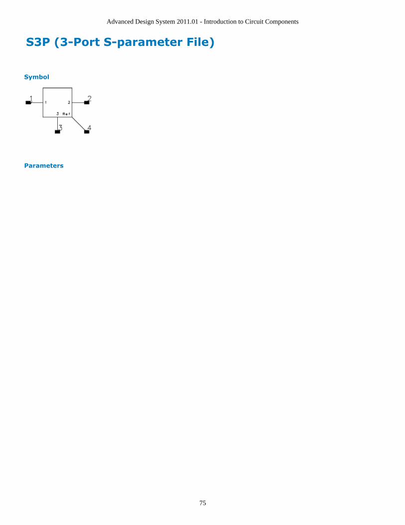
Advanced Design System 2011.01 - Introduction to Circuit Components
75
S3P (3-Port S-parameter File)
Symbol
Parameters

Advanced Design System 2011.01 - Introduction to Circuit Components
76
Name Description Units Default
File Name Name of data file containing 3-port S-, Y-, or Z-parameters forthis component. The file extension and directory path areoptional. Default extension is .s3p and the default directory is<wrk>/data where <wrk> is your current workspace directory.
None None
File Type File type: Touchstone, Dataset, CITIfile None Touchstone
Block Name (for Type=Dataset) Name of S-parameter data block None None
Interpolation Method(or InterpMode)
Interpolation method: Linear or 0, Cubic Spline or 1, Cubic or 2,Floor Value Lookup or 4, Ceiling Value Lookup or 5, Floor ValueLookup or 6
None 0
Interpolation Domain(or InterpDom)
Interpolation domain: Data Based, Rectangular, Polar, DB None Data Based
Extrapolation Method(or ExtrapMode)
Extrapolation method: Interpolation Mode, ConstantExtrapolation
None ConstantExtrapolation
Temp Physical temperature °C 27.0
CheckPassivity Check passivity or not. Yes=check; No=do not check None no
ImpNoncausalLength Non-causal function impulse response order (value type:integer)
None None
ImpMode Convolution mode (value type: integer) None None
ImpMaxFreq Maximum frequency to which device is evaluated None
ImpDeltaFreq Sample spacing in frequency None
ImpMaxOrder Maximum impulse response order (value type: integer) None None
ImpWindow Smoothing window (value type: integer) None None
ImpRelTol Relative impulse response truncation factor None None
ImpAbsTol Absolute impulse response truncation factor None None
EnforcePassivity Sets passivity enforcement for S-parameters intransient/convolution simulations. If Yes is selected, passivity inthis particular component is enforced. If No is selected,passivity is not enforced. If Auto is selected, the decision followsthe setting of ImpEnforcePassivity in the Transient controller.This setting overwrites ImpEnforcePassivity in the Transientcontroller for only this component.
None Auto
Display Display parameter on schematic: File, Type, Block, InterpMode,InterpDom, extrapMode, Temp, UseLogFreq, CheckPassivity,ImpNoncausalLength, ImpMode, ImpMaxFreq, ImpDeltaFreq,ImpMaxOrder, ImpWindow, ImpRelTol, ImpAbsTol
None File
Notes/Equations
For information on data file formats, refer to Working with Data Files (cktsim).1.When an SnP component references a CITIfile, and there is more than one data block2.in the CITIfile, the simulator picks the first data block as S-parameter data. If thefirst data block is not S-parameter data, an error message might be reported bySNPC_COMPONENT_NAME.CMP1.Block is used only when Type=Dataset. Specify the name of an S-parameter data3.block when there are multiple S-parameter data blocks in a dataset file. If Blockremains blank, the first S-parameter data block in the dataset file will be used.For the InterpMode parameter: interpolation of S-, Y-, or Z-parameters, PortZ4.reference impedance (and noise parameters for S2P) vs. simulation variable freq canbe linear, cubic spline, cubic, or lookup by actual freq value. The two parts of eachcomplex parameter (RI, MA, dBA) are interpolated independently.InterpDom defines the domains in that the two parts of a complex dependent5.

Advanced Design System 2011.01 - Introduction to Circuit Components
77
variable are interpolated:Rectangular: transform to (real, imag) before interpolationPolar: transform to (mag, angle) before interpolationDB: transform to (dB, angle) before interpolationData Based: (Series IV compatibility) uses Polar for S-parameters, Rectangular for Y-and Z-parametersExtrapMode specifies the extrapolation mode. An extrapolation warning is issued6.when an extrapolation occurs on freq in an S-parameter simulation. For all otheranalysis types, status level in the analysis controller must be set to 3 or higher to seeextrapolation warnings.Interpolation Mode: when extrapolation occurs, the interpolation mode specified byInterpMode is used for extrapolation.Constant Extrapolation: when extrapolation occurs, no interpolation is performed; thevalue of the nearest data point is returned.If the component temperature Temp is less than -273°C, then the component does7.not generate any noise. If the S-parameters describe a passive device, then Tempand Twiss's theorem are used to calculate its noise performance. If the S-parametersdescribe an active device, no noise is generated.Allowed values for ImpMode are 1 (Discrete) and 2 (PWL Continuous).8.Allowed values for ImpWindow are 0 (Rectangle) and 1 (Hanning).If these values are not specified, they default to the corresponding global parametervalues specified by the transient analysis controller item.Ref pin 4 is the common terminal; it is normally grounded, but can be used in non-9.grounded mode.For time-domain analysis, the frequency-domain S-parameters are used.10.This component has no default artwork associated with it.11.

Advanced Design System 2011.01 - Introduction to Circuit Components
78
S4P (4-Port S-parameter File)
Symbol
Parameters
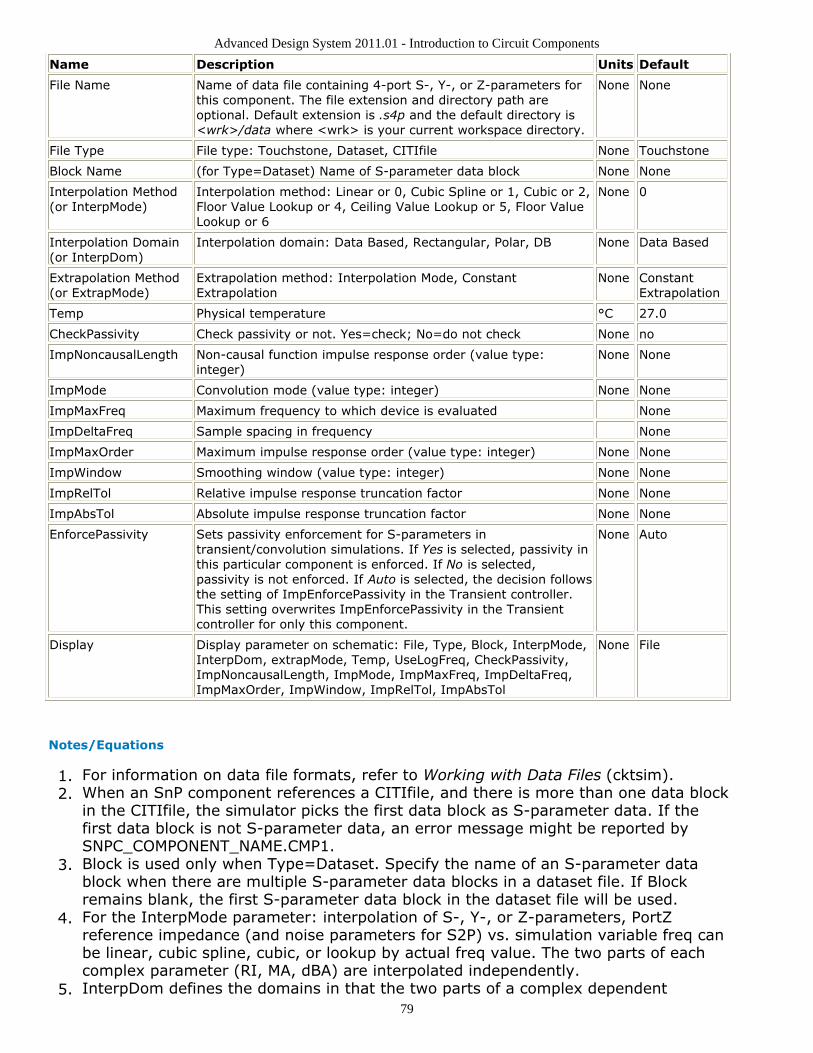
Advanced Design System 2011.01 - Introduction to Circuit Components
79
Name Description Units Default
File Name Name of data file containing 4-port S-, Y-, or Z-parameters forthis component. The file extension and directory path areoptional. Default extension is .s4p and the default directory is<wrk>/data where <wrk> is your current workspace directory.
None None
File Type File type: Touchstone, Dataset, CITIfile None Touchstone
Block Name (for Type=Dataset) Name of S-parameter data block None None
Interpolation Method(or InterpMode)
Interpolation method: Linear or 0, Cubic Spline or 1, Cubic or 2,Floor Value Lookup or 4, Ceiling Value Lookup or 5, Floor ValueLookup or 6
None 0
Interpolation Domain(or InterpDom)
Interpolation domain: Data Based, Rectangular, Polar, DB None Data Based
Extrapolation Method(or ExtrapMode)
Extrapolation method: Interpolation Mode, ConstantExtrapolation
None ConstantExtrapolation
Temp Physical temperature °C 27.0
CheckPassivity Check passivity or not. Yes=check; No=do not check None no
ImpNoncausalLength Non-causal function impulse response order (value type:integer)
None None
ImpMode Convolution mode (value type: integer) None None
ImpMaxFreq Maximum frequency to which device is evaluated None
ImpDeltaFreq Sample spacing in frequency None
ImpMaxOrder Maximum impulse response order (value type: integer) None None
ImpWindow Smoothing window (value type: integer) None None
ImpRelTol Relative impulse response truncation factor None None
ImpAbsTol Absolute impulse response truncation factor None None
EnforcePassivity Sets passivity enforcement for S-parameters intransient/convolution simulations. If Yes is selected, passivity inthis particular component is enforced. If No is selected,passivity is not enforced. If Auto is selected, the decision followsthe setting of ImpEnforcePassivity in the Transient controller.This setting overwrites ImpEnforcePassivity in the Transientcontroller for only this component.
None Auto
Display Display parameter on schematic: File, Type, Block, InterpMode,InterpDom, extrapMode, Temp, UseLogFreq, CheckPassivity,ImpNoncausalLength, ImpMode, ImpMaxFreq, ImpDeltaFreq,ImpMaxOrder, ImpWindow, ImpRelTol, ImpAbsTol
None File
Notes/Equations
For information on data file formats, refer to Working with Data Files (cktsim).1.When an SnP component references a CITIfile, and there is more than one data block2.in the CITIfile, the simulator picks the first data block as S-parameter data. If thefirst data block is not S-parameter data, an error message might be reported bySNPC_COMPONENT_NAME.CMP1.Block is used only when Type=Dataset. Specify the name of an S-parameter data3.block when there are multiple S-parameter data blocks in a dataset file. If Blockremains blank, the first S-parameter data block in the dataset file will be used.For the InterpMode parameter: interpolation of S-, Y-, or Z-parameters, PortZ4.reference impedance (and noise parameters for S2P) vs. simulation variable freq canbe linear, cubic spline, cubic, or lookup by actual freq value. The two parts of eachcomplex parameter (RI, MA, dBA) are interpolated independently.InterpDom defines the domains in that the two parts of a complex dependent5.

Advanced Design System 2011.01 - Introduction to Circuit Components
80
variable are interpolated:Rectangular: transform to (real, imag) before interpolationPolar: transform to (mag, angle) before interpolationDB: transform to (dB, angle) before interpolationData Based: (Series IV compatibility) uses Polar for S-parameters, Rectangular for Y-and Z-parametersExtrapMode specifies the extrapolation mode. An extrapolation warning is issued6.when an extrapolation occurs on freq in an S-parameter simulation. For all otheranalysis types, status level in the analysis controller must be set to 3 or higher to seeextrapolation warnings.Interpolation Mode: when extrapolation occurs, the interpolation mode specified byInterpMode is used for extrapolation.Constant Extrapolation: when extrapolation occurs, no interpolation is performed; thevalue of the nearest data point is returned.If the component temperature Temp is less than -273°C, then the component does7.not generate any noise. If the S-parameters describe a passive device, then Tempand Twiss's theorem are used to calculate its noise performance. If the S-parametersdescribe an active device, no noise is generated.Allowed values for ImpMode are 1 (Discrete) and 2 (PWL Continuous).8.Allowed values for ImpWindow are 0 (Rectangle) and 1 (Hanning).If these values are not specified, they default to the corresponding global parametervalues specified by the transient analysis controller item.Ref pin 5 is the common terminal; it is normally grounded, but can be used in non-9.grounded mode.For time-domain analysis, the frequency-domain S-parameters are used.10.This component has no default artwork associated with it.11.

Advanced Design System 2011.01 - Introduction to Circuit Components
81
S5P to S9P (5-Port to 9-Port S-parameter File)
Symbol
Parameters

Advanced Design System 2011.01 - Introduction to Circuit Components
82
Name Description Units Default
File Name Name of data file containing 5 to 9-port S-, Y-, or Z-parametersfor this component. The file extension and directory path areoptional. Default extension is .s<#>p where # ranges from 5 to9 and the default directory is <wrk>/data where <wrk> is yourcurrent workspace directory.
None None
File Type File type: Touchstone, Dataset, CITIfile None Touchstone
Block Name (for Type=Dataset) Name of S-parameter data block None None
Interpolation Method(or InterpMode)
Interpolation method: Linear or 0, Cubic Spline or 1, Cubic or 2,Floor Value Lookup or 4, Ceiling Value Lookup or 5, Floor ValueLookup or 6
None 0
Interpolation Domain(or InterpDom)
Interpolation domain: Data Based, Rectangular, Polar, DB None Data Based
Extrapolation Method(or ExtrapMode)
Extrapolation method: Interpolation Mode, ConstantExtrapolation
None ConstantExtrapolation
Temp Physical temperature °C 27.0
CheckPassivity Check passivity or not. Yes=check; No=do not check None no
ImpNoncausalLength Non-causal function impulse response order (value type:integer)
None None
ImpMode Convolution mode (value type: integer) None None
ImpMaxFreq Maximum frequency to which device is evaluated None
ImpDeltaFreq Sample spacing in frequency None
ImpMaxOrder Maximum impulse response order (value type: integer) None None
ImpWindow Smoothing window (value type: integer) None None
ImpRelTol Relative impulse response truncation factor None None
ImpAbsTol Absolute impulse response truncation factor None None
EnforcePassivity Sets passivity enforcement for S-parameters intransient/convolution simulations. If Yes is selected, passivity inthis particular component is enforced. If No is selected,passivity is not enforced. If Auto is selected, the decision followsthe setting of ImpEnforcePassivity in the Transient controller.This setting overwrites ImpEnforcePassivity in the Transientcontroller for only this component.
None Auto
Display Display parameter on schematic: File, Type, Block, InterpMode,InterpDom, extrapMode, Temp, UseLogFreq, CheckPassivity,ImpNoncausalLength, ImpMode, ImpMaxFreq, ImpDeltaFreq,ImpMaxOrder, ImpWindow, ImpRelTol, ImpAbsTol
None File
Notes/Equations
For information on data file formats, refer to Working with Data Files (cktsim).1.The number of terminals increases sequentially from 5 to 9, and is equal to the2.number of ports of the component.Ref is the common terminal; it is normally grounded, but can be used in non-grounded mode.If no extension is supplied with the file name, then a default value of ".s(#)p" is3.used, where (#) is the number of ports of the component.When an SnP component references a CITIfile, and there is more than one data block4.in the CITIfile, the simulator picks the first data block as S-parameter data. If thefirst data block is not S-parameter data, an error message might be reported bySNPC_COMPONENT_NAME.CMP1.Block is used only when Type=Dataset. Specify the name of an S-parameter data5.

Advanced Design System 2011.01 - Introduction to Circuit Components
83
block when there are multiple S-parameter data blocks in a dataset file. If Blockremains blank, the first S-parameter data block in the dataset file will be used.For the InterpMode parameter: interpolation of S-, Y-, or Z-parameters, PortZ6.reference impedance (and noise parameters for S2P) vs. simulation variable freq canbe linear, cubic spline, cubic, or lookup by actual freq value. The two parts of eachcomplex parameter (RI, MA, dBA) are interpolated independently.InterpDom defines the domains in that the two parts of a complex dependent7.variable are interpolated:Rectangular: transform to (real, imag) before interpolationPolar: transform to (mag, angle) before interpolation.DB: transform to (dB, angle) before interpolationData Based: (Series IV compatibility) uses Polar for S-parameters, Rectangular for Y-and Z-parametersExtrapMode specifies the extrapolation mode. An extrapolation warning is issued8.when an extrapolation occurs on freq in an S-parameter simulation. For all otheranalysis types, status level in the analysis controller must be set to 3 or higher to seeextrapolation warnings.Interpolation Mode: when extrapolation occurs, the interpolation mode specified byInterpMode is used for extrapolation.Constant Extrapolation: when extrapolation occurs, no interpolation is performed; thevalue of the nearest data point is returned.If the component temperature Temp is less than -273°C, then the component does9.not generate any noise. If the S-parameters describe a passive device, then Tempand Twiss's theorem are used to calculate its noise performance. If the S-parametersdescribe an active device, no noise is generated.Allowed values for ImpMode are 1 (Discrete) and 2 (PWL Continuous).10.Allowed values for ImpWindow are 0 (Rectangle) and 1 (Hanning).If these values are not specified, they default to the corresponding global parametervalues specified by the transient analysis controller item.For time-domain analysis, the frequency-domain S-parameters are used.11.This component has no default artwork associated with it.12.

Advanced Design System 2011.01 - Introduction to Circuit Components
84
S10P to S20P (10-Port to 20-Port S-parameter File)
Symbol
Parameters

Advanced Design System 2011.01 - Introduction to Circuit Components
85
Name Description Units Default
File Name Name of data file containing 10 to 20-port S-, Y-, or Z-parameters for this component. The file extension and directorypath are optional. Default extension is .s<#>p where # rangesfrom 10 to 20 and the default directory is <wrk>/data where<wrk> is your current workspace directory.
None None
File Type File type: Touchstone, Dataset, CITIfile None Touchstone
Block Name (for Type=Dataset) Name of S-parameter data block None None
Interpolation Method(or InterpMode)
Interpolation method: Linear or 0, Cubic Spline or 1, Cubic or 2,Floor Value Lookup or 4, Ceiling Value Lookup or 5, Floor ValueLookup or 6
None 0
Interpolation Domain(or InterpDom)
Interpolation domain: Data Based, Rectangular, Polar, DB None Data Based
Extrapolation Method(or ExtrapMode)
Extrapolation method: Interpolation Mode, ConstantExtrapolation
None ConstantExtrapolation
Temp Physical temperature °C 27.0
CheckPassivity Check passivity or not. Yes=check; No=do not check None no
ImpNoncausalLength Non-causal function impulse response order (value type:integer)
None None
ImpMode Convolution mode (value type: integer) None None
ImpMaxFreq Maximum frequency to which device is evaluated None
ImpDeltaFreq Sample spacing in frequency None
ImpMaxOrder Maximum impulse response order (value type: integer) None None
ImpWindow Smoothing window (value type: integer) None None
ImpRelTol Relative impulse response truncation factor None None
ImpAbsTol Absolute impulse response truncation factor None None
EnforcePassivity Sets passivity enforcement for S-parameters intransient/convolution simulations. If Yes is selected, passivity inthis particular component is enforced. If No is selected,passivity is not enforced. If Auto is selected, the decision followsthe setting of ImpEnforcePassivity in the Transient controller.This setting overwrites ImpEnforcePassivity in the Transientcontroller for only this component.
None Auto
Display Display parameter on schematic: File, Type, Block, InterpMode,InterpDom, extrapMode, Temp, UseLogFreq, CheckPassivity,ImpNoncausalLength, ImpMode, ImpMaxFreq, ImpDeltaFreq,ImpMaxOrder, ImpWindow, ImpRelTol, ImpAbsTol
None File
Notes/Equations
The items S11P through S99P cannot be selected from the component palette. They1.are accessed by typing the appropriate name (such as S12P or S98P) into the rightentry box (directly above the viewing area), pressing Enter , then moving the cursorto the viewing area to place the item.The number of terminals increases sequentially from 10 to 20, and is equal to the2.number of ports of the component.Ref is the common terminal; it is normally grounded, but can be used in non-grounded mode.For information on data file formats, refer to Working with Data Files (cktsim).3.If no extension is supplied with the File name, then a default value of .s( # )p is4.used, where (#) is the number of ports of the component.When an SnP component references a CITIfile, and there is more than one data block5.
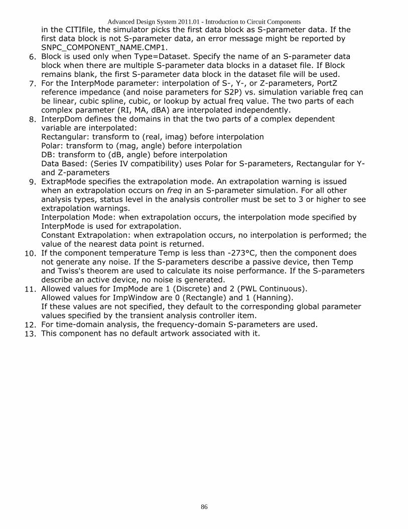
Advanced Design System 2011.01 - Introduction to Circuit Components
86
in the CITIfile, the simulator picks the first data block as S-parameter data. If thefirst data block is not S-parameter data, an error message might be reported bySNPC_COMPONENT_NAME.CMP1.Block is used only when Type=Dataset. Specify the name of an S-parameter data6.block when there are multiple S-parameter data blocks in a dataset file. If Blockremains blank, the first S-parameter data block in the dataset file will be used.For the InterpMode parameter: interpolation of S-, Y-, or Z-parameters, PortZ7.reference impedance (and noise parameters for S2P) vs. simulation variable freq canbe linear, cubic spline, cubic, or lookup by actual freq value. The two parts of eachcomplex parameter (RI, MA, dBA) are interpolated independently.InterpDom defines the domains in that the two parts of a complex dependent8.variable are interpolated:Rectangular: transform to (real, imag) before interpolationPolar: transform to (mag, angle) before interpolationDB: transform to (dB, angle) before interpolationData Based: (Series IV compatibility) uses Polar for S-parameters, Rectangular for Y-and Z-parametersExtrapMode specifies the extrapolation mode. An extrapolation warning is issued9.when an extrapolation occurs on freq in an S-parameter simulation. For all otheranalysis types, status level in the analysis controller must be set to 3 or higher to seeextrapolation warnings.Interpolation Mode: when extrapolation occurs, the interpolation mode specified byInterpMode is used for extrapolation.Constant Extrapolation: when extrapolation occurs, no interpolation is performed; thevalue of the nearest data point is returned.If the component temperature Temp is less than -273°C, then the component does10.not generate any noise. If the S-parameters describe a passive device, then Tempand Twiss's theorem are used to calculate its noise performance. If the S-parametersdescribe an active device, no noise is generated.Allowed values for ImpMode are 1 (Discrete) and 2 (PWL Continuous).11.Allowed values for ImpWindow are 0 (Rectangle) and 1 (Hanning).If these values are not specified, they default to the corresponding global parametervalues specified by the transient analysis controller item.For time-domain analysis, the frequency-domain S-parameters are used.12.This component has no default artwork associated with it.13.

Advanced Design System 2011.01 - Introduction to Circuit Components
87
S21P to S99P (21-Port to 99-Port S-parameter File) Symbol
Parameters

Advanced Design System 2011.01 - Introduction to Circuit Components
88
Name Description Units Default
File Name Name of data file containing 21 to 99-port S-, Y-, or Z-parameters for this component. The file extension and directorypath are optional. Default extension is .s<#>p where # rangesfrom 21 to 99 and the default directory is <wrk>/data where<wrk> is your current workspace directory.
None None
File Type File type: Touchstone, Dataset, CITIfile None Touchstone
Block Name (for Type=Dataset) Name of S-parameter data block None None
Interpolation Method(or InterpMode)
Interpolation method: Linear or 0, Cubic Spline or 1, Cubic or 2,Floor Value Lookup or 4, Ceiling Value Lookup or 5, Floor ValueLookup or 6
None 0
Interpolation Domain(or InterpDom)
Interpolation domain: Data Based, Rectangular, Polar, DB None Data Based
Extrapolation Method(or ExtrapMode)
Extrapolation method: Interpolation Mode, ConstantExtrapolation
None ConstantExtrapolation
Temp Physical temperature °C 27.0
CheckPassivity Check passivity or not. Yes=check; No=do not check None no
ImpNoncausalLength Non-causal function impulse response order (value type:integer)
None None
ImpMode Convolution mode (value type: integer) None None
ImpMaxFreq Maximum frequency to which device is evaluated None
ImpDeltaFreq Sample spacing in frequency None
ImpMaxOrder Maximum impulse response order (value type: integer) None None
ImpWindow Smoothing window (value type: integer) None None
ImpRelTol Relative impulse response truncation factor None None
ImpAbsTol Absolute impulse response truncation factor None None
EnforcePassivity Sets passivity enforcement for S-parameters intransient/convolution simulations. If Yes is selected, passivity inthis particular component is enforced. If No is selected, passivityis not enforced. If Auto is selected, the decision follows thesetting of ImpEnforcePassivity in the Transient controller. Thissetting overwrites ImpEnforcePassivity in the Transientcontroller for only this component.
None Auto
Display Display parameter on schematic: File, Type, Block, InterpMode,InterpDom, extrapMode, Temp, UseLogFreq, CheckPassivity,ImpNoncausalLength, ImpMode, ImpMaxFreq, ImpDeltaFreq,ImpMaxOrder, ImpWindow, ImpRelTol, ImpAbsTol
None File
Notes/Equations
S11P through S99P support up to 99-port networks. They cannot be selected from1.the component palette; they are accessed by typing the appropriate name (such asS11P or S99P) into the field above the viewing area, pressing Enter, then moving thecursor to the viewing area to place the item.Ref is the common terminal; it is normally grounded, but can be used in non-2.grounded mode.The S, Y, Z, and N matrix measurements are allowed for up to 99-port networks. In3.addition, single measurements are applicable:SIJ, for example (S(29,28))VSWR, for example (S(29,29))These components primarily support electromagnetic simulation results of circuits4.with a large number of ports, such as antenna feed networks.When an SnP component references a CITIfile, and there is more than one data block5.in the CITIfile, the simulator picks the first data block as S-parameter data. If the

Advanced Design System 2011.01 - Introduction to Circuit Components
89
first data block is not S-parameter data, an error message might be reported bySNPC_COMPONENT_NAME.CMP1.Block is used only when Type=Dataset. Specify the name of an S-parameter data6.block when there are multiple S-parameter data blocks in a dataset file. If Blockremains blank, the first S-parameter data block in the dataset file will be used.For the InterpMode parameter: interpolation of S-, Y-, or Z-parameters, PortZ7.reference impedance (and noise parameters for S2P) vs. simulation variable freq canbe linear, cubic spline, cubic, or lookup by actual freq value. The two parts of eachcomplex parameter (RI, MA, dBA) are interpolated independently.InterpDom defines the domains in that the two parts of a complex dependent8.variable are interpolated:Rectangular: transform to (real, imag) before interpolationPolar: transform to (mag, angle) before interpolationDB: transform to (dB, angle) before interpolationData Based: (Series IV compatibility) uses Polar for S-parameters, Rectangular for Y-and Z-parametersExtrapMode specifies the extrapolation mode. An extrapolation warning is issued9.when an extrapolation occurs on freq in an S-parameter simulation. For all otheranalysis types, status level in the analysis controller must be set to 3 or higher to seeextrapolation warnings.Interpolation Mode: when extrapolation occurs, the interpolation mode specified byInterpMode is used for extrapolation.Constant Extrapolation: when olation occurs, no interpolation is performed; the valueof the nearest data point is returned.If the component temperature Temp is less than -273°C, then the component does10.not generate any noise. If the S-parameters describe a passive device, then Tempand Twiss's theorem are used to calculate its noise performance. If the S-parametersdescribe an active device, no noise is generated.Allowed values for ImpMode are 1 (Discrete) and 2 (PWL Continuous).11.Allowed values for ImpWindow are 0 (Rectangle) and 1 (Hanning).If these values are not specified, they default to the corresponding global parametervalues specified by the transient analysis controller item.For time-domain analysis, the frequency-domain S-parameters are used.12.This component has no default artwork associated with it.13.

Advanced Design System 2011.01 - Introduction to Circuit Components
90
SnP component (n>99) Symbol
Parameters

Advanced Design System 2011.01 - Introduction to Circuit Components
91
Name Description Units Default
File Name Name of data file containing 1-port S-, Y-, or Z-parameters forthis component. The file extension and directory path areoptional. Default extension is .s1p and the default directory is<wrk>/data where <wrk> is your current workspace directory.
None None
File Type File type: Touchstone, Dataset, CITIfile None Touchstone
Block Name (for Type=Dataset) Name of S-parameter data block None None
Interpolation Method(or InterpMode)
Interpolation method: Linear or 0, Cubic Spline or 1, Cubic or 2,Floor Value Lookup or 4, Ceiling Value Lookup or 5, Floor ValueLookup or 6
None 0
Interpolation Domain(or InterpDom)
Interpolation domain: Data Based, Rectangular, Polar, DB None Data Based
Extrapolation Method(or ExtrapMode)
Extrapolation method: Interpolation Mode, ConstantExtrapolation
None ConstantExtrapolation
Temp Physical temperature °C 27.0
CheckPassivity Check passivity of the S-parameter data or not. Yes=check;No=do not check
None no
ImpNoncausalLength Non-causal function impulse response order (value type:integer)
None None
ImpMode Convolution mode (value type: integer) None None
ImpMaxFreq Maximum frequency to which device is evaluated None
ImpDeltaFreq Sample spacing in frequency None
ImpMaxOrder Maximum impulse response order (value type: integer) None None
ImpWindow Smoothing window (value type: integer) None None
ImpRelTol Relative impulse response truncation factor None None
ImpAbsTol Absolute impulse response truncation factor None None
EnforcePassivity Sets passivity enforcement for S-parameters intransient/convolution simulations. If Yes is selected, passivity inthis particular component is enforced. If No is selected, passivityis not enforced. If Auto is selected, the decision follows thesetting of ImpEnforcePassivity in the Transient controller. Thissetting overwrites ImpEnforcePassivity in the Transientcontroller for only this component.
None Auto
Display Display parameter on schematic: File, Type, Block, InterpMode,InterpDom, extrapMode, Temp, UseLogFreq, CheckPassivity,ImpNoncausalLength, ImpMode, ImpMaxFreq, ImpDeltaFreq,ImpMaxOrder, ImpWindow, ImpRelTol, ImpAbsTol
None File
Notes/Equations
SnP component (n>99) is used to create SnP components with a port number larger1.than 99.SnP(n>99) component is not a built-in component. SnP(n>99) components cannot2.be selected from the Data Items component library palette (which is the case forn=1:10), nor can they be typed into the field above the design viewing area (which isthe case for n=10:99). Instead, for n>99, you must create SnP components byfollowing the procedure given in the Example section below.

Advanced Design System 2011.01 - Introduction to Circuit Components
92
TipWhen an SnP component references a CITIfile, and there is more than one data block in the1.CITIfile, the simulator picks the first data block as S-parameter data. If the first data block isnot S-parameter data, an error message might be reported bySNPC_COMPONENT_NAME.CMP1.An extrapolation warning is issued when an extrapolation occurs on freq in an S-parameter2.simulation. For all other analysis types, status level in the analysis controller must be set to 3or higher to see extrapolation warnings.
Example
Procedure for ADS2011
From the Main window select Tools > Command Line and type:1.generate_snp_component(112 , "MyLibrary")where:112 is the number of the ports."MyLibrary" is the name of the library you want the new component to be created in.This generates all the required files including a new cell S112P in the specified libraryand a file S112P in the workspace directory and loads the device into ADS.Type the name of the component (e.g., S112P) in the schematic component history2.list to place it into the Schematic window.
To delete a SnP component, all the files generated using the procedures described aboveneed to be deleted.These are the Cell SnP and the file <curr_wrk>/SnP.

Advanced Design System 2011.01 - Introduction to Circuit Components
93
SnP_Diff component Description
Unlike SnP components which have one global reference node and only the "plus"terminals for each port, SnP_Diff components are SnP Data Items which have twoterminals (plus/minus) per port models.
NoteThe SnP_Diff component is not a differential (or mixed-mode) SnP component. Since the minus terminalsof an SnP_Diff component can be connected to nodes other than Ground, caution must be taken whenusing the component. Incoming current through the plus terminals must be the same as the currentleaving through the minus terminals. If this requirement is violated, S-parameter data will be useless.
Symbol
Parameters
Advanced Design System 2011.01 - Introduction to Circuit Components
94
Name Description Units Default
File Name Name of data file containing # - port S-, Y-, or Z-parameters for thiscomponent. The file extension and directory path are optional. Defaultextension is .s#p and the default directory is <wrk>/data where<wrk> is your current workspace directory.
None None
File Type File type: Touchstone, Dataset, CITIfile None None
Block Name (for Type=Dataset) Name of S-parameter data block None None
InterpMode Interpolation mode: Linear, Cubic Spline, Cubic, Value Lookup None None
InterpDom Interpolation domain: Data Based (polar for S and rectangular for Yand Z), Rectangular, Polar, DB
None None
ExtrapMode Extrapolation mode: Interpolation Mode, Constant Extrapolation None None
Temp Physical temperature °C Celsius
ImpNoncausalLength Non-causal function impulse response order Integer None
ImpMode Convolution mode Integer None
ImpMaxFreq Maximum frequency to which device is evaluated None
ImpDeltaFreq Sample spacing in frequency None
ImpMaxOrder Maximum impulse response order Integer None
ImpWindow Smoothing window Integer None
ImpRelTol Relative impulse response truncation factor None None
ImpAbsTol Absolute impulse response truncation factor None None
EnforcePassivity Sets passivity enforcement for S-parameters in transient/convolutionsimulations. If Yes is selected, passivity in this particular component isenforced. If No is selected, passivity is not enforced. If Auto isselected, the decision follows the setting of ImpEnforcePassivity in theTransient controller. This setting overwrites ImpEnforcePassivity in theTransient controller for only this component.
None Auto
Notes/Equations
SnP_Diff components cannot be selected from the component palette; they are1.accessed by typing the appropriate name (such as S12P_Diff) into the field above theviewing area and press Enter, then moving the cursor to the viewing area to placethe itemSnP_Diff component is not a built-in component. You must create this component by2.following the procedure given below
Procedure for ADS2011
From the Main window select Tools > Command Line and type:1.generate_snp_diff_component(12 , "MyLibrary")where:12 is the number of the ports."MyLibrary" is the name of the library you want the new component to be created in.This generates all the required files including a new cell S12P_Diff in the specifiedlibrary and a file S12P_Diff in the workspace directory and loads the device into ADS.Type the name of the component (e.g., S12P_Diff) in the schematic component2.history list to place it into the Schematic window.
To delete a SnP_Diff component, all the files generated using the procedures describedabove need to be deleted.These are the Cell SnP_Diff and the file <curr_wrk>/SnP_Diff

Advanced Design System 2011.01 - Introduction to Circuit Components
95
HintAn extrapolation warning is issued when an extrapolation occurs on freq in an S-parameter simulation. Forall other analysis types, status level in the analysis controller must be set to 3 or higher to seeextrapolation warnings.

Advanced Design System 2011.01 - Introduction to Circuit Components
96
VAR (Variables and Equations Component) Symbol
Parameters
Name Description Units Default
X Name of variable or equation None 1.0
Notes/Equations
A schematic can include any number of VAR items. A VAR item can define multiple1.variables or equations.All variables and equations have the form LHS=RHS, where LHS is the name of thevariable or equation to the left of the equality symbol = ; RHS is the value orexpression to the right of the equality symbol. Variable and equation names (LHS)must begin with a letter and cannot exceed 32 characters. Names cannot begin withan underscore (_) unless it is one of the program-reserved variables explained later.Names are case sensitive; for example, X and x are different names.
NoteThere is a limitation of 1800 characters in a variable equation. Using more than 1800 charactersmay cause ADS to crash.
Variable or Equation Entry Mode2.Name=Value. Equations are defined when Variable or Equation Entry Mode is set toName=Value and multiple variables and equations can be entered into the fieldprovided. Equation values (RHS) must be an expression that equates to a numeric ora string value. An equation numeric value can be complex and the complex operator jis recognized; for example, z = x + j*y, where x and y can be real or complexnumbers or functions. The equation value can use built-in constants (refer to note 3)and functions (refer to note 4).

Advanced Design System 2011.01 - Introduction to Circuit Components
97
Standard. Variables are defined when the Variable or Equation Entry Mode is set toStandard, a single variable can be entered into the fields provided. Variable Valuemust be a numeric value (2.567, for example) or a string value enclosed in double-quote symbols. For example, the string value for a precision type of parameter canbe defined as 2.14 for Signal Processing, or "MSUB1" for Circuit. Variable values canalso be defined as a nominal value with associated optimization range.
File Based. To use variable or equation data from a file, reference aDataAccessComponent placed in your currently active design. For more informationon the use of DAC data files, refer to DataAccessComponent.Name is the name of the variable to be created, as identified in theDataAccessComponent. Data Access Component Instance is the instance name of the
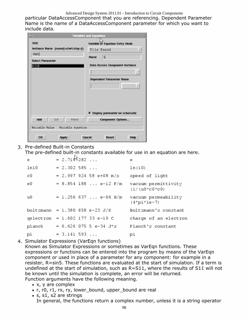
Advanced Design System 2011.01 - Introduction to Circuit Components
98
particular DataAccessComponent that you are referencing. Dependent ParameterName is the name of a DataAccessComponent parameter for which you want toinclude data.
Pre-defined Built-in Constants3.The pre-defined built-in constants available for use in an equation are here.
Simulator Expressions (VarEqn functions)4.Known as Simulator Expressions or sometimes as VarEqn functions. Theseexpressions or functions can be entered into the program by means of the VarEqncomponent or used in place of a parameter for any component: for example in aresister, R=sin5. These functions are evaluated at the start of simulation. If a term isundefined at the start of simulation, such as R=S11, where the results of S11 will notbe known until the simulation is complete, an error will be returned.Function arguments have the following meaning.
x, y are complexr, r0, r1, rx, ry, lower_bound, upper_bound are reals, s1, s2 are stringsIn general, the functions return a complex number, unless it is a string operator
Advanced Design System 2011.01 - Introduction to Circuit Components
99
as noted. Refer to Introduction to Simulator Expressions (expsim) for a completelist of simulator expressions. A function that returns a real value effectively hasa zero value imaginary term.
Equation Editor Syntax5.Mathematical expressions entered equations can include the following items.
Blank spaces Blank spaces within an expression are ignored; they can be usedto improve readability. For example,4 * (x + .1) evaluates the same as4*(x+.1)Numerical constants Real numbers such as 12.68, exponential notation numberssuch as 1e6 or 25.1e3, pi can be used, and complex numbers can be defined.For example, z = x + j*y.LHS form assignment The LHS assignment takes the form of integer, double,complex or string dependent on what form is associated with the RHS. Forexample,X=4, Y=4.0, W=1.0+j*3.0, Z="4"associates the form of integer, double, complex and string to X, Y, W and Z,respectively. The LHS form is important when subsequently used in followingexpressions.Mathematical operators Standard operators are available:
** exponentiation
exponentiation
* multiplication
/ division
+ addition
- subtraction
NoteTo avoid returning incorrect results when using ** with very large integers, convert integersto real numbers first.
In evaluating an expression, operator precedence is: ** * / + - .Operators at the same level (for example * / ) are evaluated left to right.Any number of parentheses pairs can be used to modify an expression in theusual way. For exampleC10 * (1 + .005) evaluates differently thanC10 *1 + .005
Parameters of a parametric subnetwork Any formal parameters that are passed into aparametric subnetwork can be included in equations defined in that subnetwork.These parameters are defined for a schematic view using the File > DesignParameters menu selection.Use of if...then...else...endif statements An equation can use a conditional statement:if ( conditional expression) then ( expression1) else (expression2) endif. Forexample,X = 1Y = if ( X>0) then ( cos( pi/8) ) else ( sin( pi/8) ) endifThe conditional expression can be a simple or complex numeric conditionalexpression with arguments separated by the standard symbols:< > <= >= = != &&Each expression can be any valid numeric expression. The entireif...then...else...endif expression must be on one line.
Scope: Nested or Global

Advanced Design System 2011.01 - Introduction to Circuit Components
100
When referencing VAR items in hierarchical designs, set the Scope option to indicate thelevels, from a hierarchical standpoint, that recognize the expressions defined in the VAR.To set Scope, click Component Options.Nested sets the scope so VAR item expressions are recognized within the designcontaining the VAR item, as well as within any subnetworks (designs at lower levels)referenced by the design containing the VAR item. This is the default.Global sets the scope so VAR item expressions are recognized throughout the entiredesign, no matter what level in the design hierarchy the VAR item is placed.
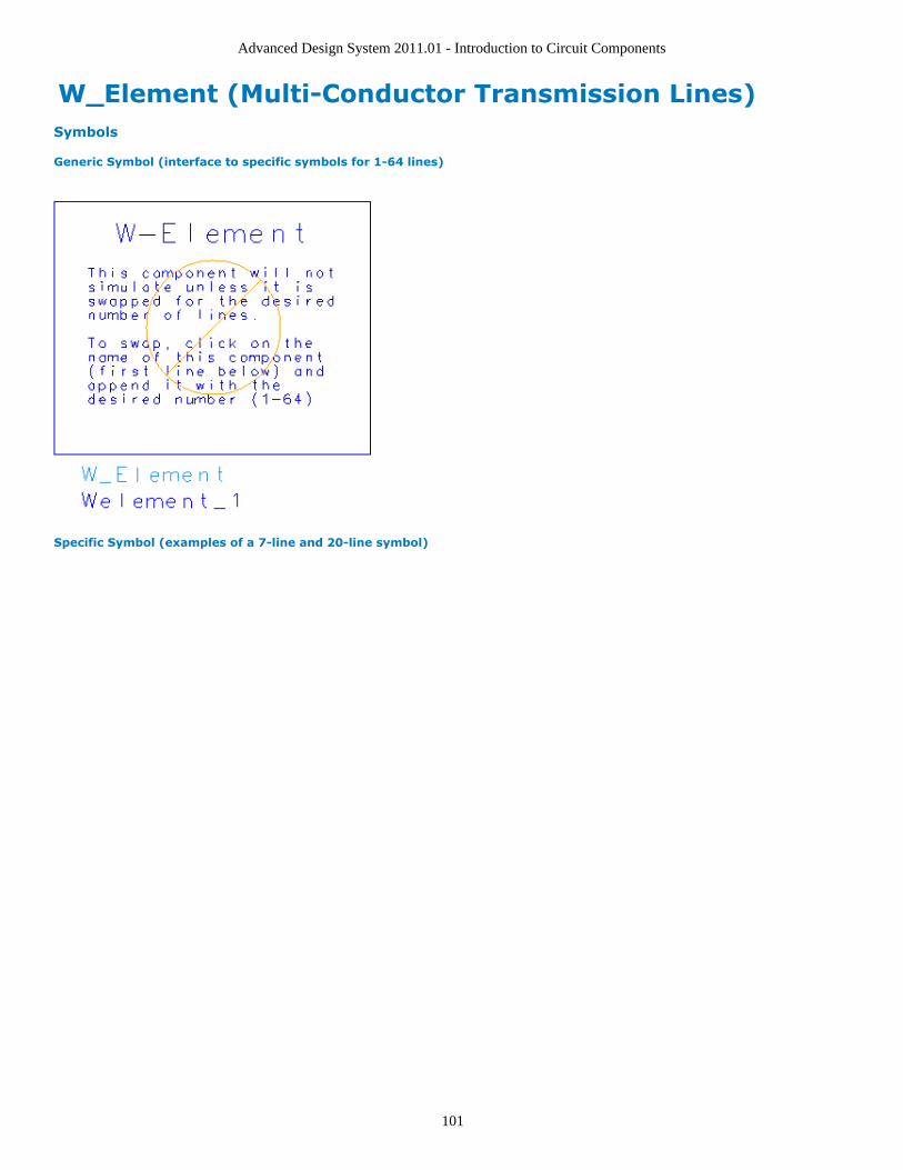
Advanced Design System 2011.01 - Introduction to Circuit Components
101
W_Element (Multi-Conductor Transmission Lines) Symbols
Generic Symbol (interface to specific symbols for 1-64 lines)
Specific Symbol (examples of a 7-line and 20-line symbol)

Advanced Design System 2011.01 - Introduction to Circuit Components
102
Signal line numbers, as shown in the symbols, are relevant to the data ordering (rows andcolumns of the RLGC matrices). Please note that the easiest way to place a specificsymbol in the Schematic window is to drop a generic symbol and edit (on screen) itsname. The generic component name "W_Element" needs to be appended with the desirednumber of lines, for example changing it to "W_Element7" or "W_Element20".
W_Element components are supported for HSPICE compatibility. For more information, see CompatibleFeatures and Limitations (hspice).
Library: Analog/RF Network > Data Items
Parameters

Advanced Design System 2011.01 - Introduction to Circuit Components
103
Parameters
Name Description Units Default
N number of transmission lines none 1
Length length of all transmission lines m 0.001
Model_type model type: 0 – analytical (static matrices) model, 1- tabular model(frequency dependent matrices)
none 0
RLGCfile name of the file containing static RLGC data (for Model_type=0) none none
Lfile name of the file containing frequency dependent L matrix (for Model_type=1) none none
Cfile name of the file containing frequency dependent C matrix (for Model_type=1) none none
Rfile name of the file containing frequency dependent R matrix (for Model_type=1) none none
Gfile name of the file containing frequency dependent G matrix (for Model_type=1) none none
Ldata array defining the L matrix (either static for Model_type=0 or frequencydependent for Model_type=1)
H/m none
Cdata array defining the C matrix (either static for Model_type=0 or frequencydependent for Model_type=1)
F/m none
Rdata array defining the R matrix (either static DC matrix Rdc for Model_type=0 orfrequency dependent matrix R for Model_type=1)
Ohm/m 0.0
Gdata array defining the G matrix (either static DC matrix Gdc for Model_type=0 orfrequency dependent matrix G for Model_type=1)
S/m 0.0
RSdata array defining the Rs matrix (applies to Model_type=0) Ohm/m 0.0
GDdata array defining the Gd matrix (applies to Model_type=0) S/m 0.0
Fgd cut-off frequency of dielectric loss (applies to Model_type=0) – zero meansinfinity
Hz infinity
LfreqSweep type of frequency sweep in Ldata array or in Lfile: 0 – linearFromTo, 1 –logFromTo, 2 – logPtsPerDec, 3 – logPtsPerOct, 4 – points (applies toModel_type=1)
none 0
LfreqStart frequency of the first dataset in the Ldata list or in Lfile (applies toModel_type=1)
Hz 0.0
LfreqStop frequency of the last dataset in the Ldata list or in Lfile (applies toModel_type=1)
Hz none
LfreqsPerDec starting from LfreqStart, the number of frequencies per decade correspondingto the subsequent datasets in Ldata or in Lfile (applies to Model_type=1)
none 10
LfreqsPerOct starting from LfreqStart, the number of frequencies per octave correspondingto the subsequent datasets in Ldata or in Lfile (applies to Model_type=1)
none 10
CfreqSweep type of frequency sweep in Cdata array or in Cfile: 0 – linearFromTo, 1 –logFromTo, 2 – logPtsPerDec, 3 – logPtsPerOct, 4 – points (applies toModel_type=1)
none 0
CfreqStart frequency of the first dataset in the Cdata list or in Cfile (applies toModel_type=1)
Hz 0.0
CfreqStop frequency of the last dataset in the Cdata list or in Cfile (applies toModel_type=1)
Hz none
CfreqsPerDec starting from CfreqStart, the number of frequencies per decade correspondingto the subsequent datasets in Cdata or in Cfile (applies to Model_type=1)
none 10
CfreqsPerOct starting from CfreqStart, the number of frequencies per octave correspondingto the subsequent datasets in Cdata or in Cfile (applies to Model_type=1)
none 10
RfreqSweep type of frequency sweep in Rdata array or in Rfile: 0 – linearFromTo, 1 –logFromTo, 2 – logPtsPerDec, 3 – logPtsPerOct, 4 – points (applies toModel_type=1)
none 0
RfreqStart frequency of the first dataset in the Rdata list or in Rfile (applies toModel_type=1)
Hz 0.0
RfreqStop frequency of the last dataset in the Rdata list or in Rfile (applies to Hz none
Advanced Design System 2011.01 - Introduction to Circuit Components
104
Model_type=1)
RfreqsPerDec starting from RfreqStart, the number of frequencies per decade correspondingto the subsequent datasets in Rdata or in Rfile (applies to Model_type=1)
none 10
RfreqsPerOct starting from RfreqStart, the number of frequencies per octave correspondingto the subsequent datasets in Rdata or in Rfile (applies to Model_type=1)
none 10
GfreqSweep type of frequency sweep in Gdata array or in Gfile: 0 – linearFromTo, 1 –logFromTo, 2 – logPtsPerDec, 3 – logPtsPerOct, 4 – points (applies toModel_type=1)
none 0
GfreqStart frequency of the first dataset in the Gdata list or in Gfile (applies toModel_type=1)
Hz 0.0
GfreqStop frequency of the last dataset in the Gdata list or in Gfile (applies toModel_type=1)
Hz none
GfreqsPerDec starting from GfreqStart, the number of frequencies per decade correspondingto the subsequent datasets in Gdata or in Gfile (applies to Model_type=1)
none 10
GfreqsPerOct starting from GfreqStart, the number of frequencies per octave correspondingto the subsequent datasets in Gdata or in Gfile (applies to Model_type=1)
none 10
Range of Usage
The diagonal entries of the L and C matrices must be positive. The off-diagonal elementsof the C, G and Gd matrices must be non-positive. The diagonal entries of R and Gmatrices must be non-negative. See Notes/Equations for further details.
Notes/Equations
The available connection nodes include a reference line, and thus the total number of1.connection nodes is 2(N+1).The matrices can be static (Model_type=0, default) or tabular frequency dependent2.(Model_type=1). For Model_type=0, all the matrices are specified either directly, orin a file. For Model_type=1, the data format can be set independently for eachmatrix.All the matrices are assumed to be symmetric and real-valued. Each matrix must be3.specified using the lower triangular part only, which contains the diagonal and sub-diagonal elements. The order is row centric, that is the first element of the first row,followed by the first two elements of the second row, then the first three elements ofthe third row, etc. The total number of the matrix element specified must be exactlyN(N+1)/2.If a file name parameter is specified, any corresponding, directly specified data will4.be ignored. For example, if RLGCfile is specified and Model_type=0 then all of Ldata,Cdata, Rdata, Gdata, RSdata and GDdata arrays, even if specified will be ignored. Ifany of the optional matrices are missing in the file, their default zero values will beused.Any of the matrices specified directly using the parameters Ldata, Cdata, Rdata,5.Gdata, RSdata and GDdata need to use the list() function with an appropriatenumber of entries (size of the array). For further details see Notes 6, 7 and 8.For Model_type=0, the size of the arrays Ldata, Cdata, Rdata, Gdata, RSdata and6.GDdata arrays must be exactly N(N+1)/2.For Model_type=1, the frequency dependent tabular data consists of a number of7.matrices (datasets). The corresponding frequencies are implicitly defined by the typeand the details of the frequency sweep. These sweeps are set individually for each ofthe matrices. For linear and logarithmic sweeps, the first entry in the data list, or inthe data file, is the number K of datasets to follow. Thus the total number of numericentries must be exactly 1+K*N*(N+1)/2.For Model_type=1 and for the "points" type of the sweep, the data consists of pairs,8.where each pair is formed by a frequency value followed by the matrix entries at that

Advanced Design System 2011.01 - Introduction to Circuit Components
105
frequency. The first data entry in the data list (or a file) is the number of such pairs(the number of points). Thus, for K points the data must contain exactly1+K*(1+N*(N+1)/2) numeric entries.The format of the data files is restricted. The files may only contain comment lines9.(or partial lines) starting with the asterisk character "*", and the numeric datawithout any units or scaling factors. The data can be delimited by one or more of thefollowing characters: " \t\n,;()[]{}". For further details see Notes 10 and 11.For Model_type=0, only the RLGCfile parameter is relevant. The first numeric entry in10.an RLGCfile must be an integer N specifying the number of lines and thus the size ofall the matrices. Only the L and C matrices are required and thus the total number ofnumeric entries must be 1+K*N*(N+1)/2 where K is an integer between 2 and 6.The order of the matrices is L, C, Rdc, Gdc, Rs and Gd.For Model_type=1, only Lfile, Cfile, Rfile and Gfile parameters are relevant. Each file11.contains frequency dependent data for one matrix type only. The number and themeaning of numeric entries in any of such files is exactly the same as in a directlyspecified array for the specified type of the frequency sweep, as in Notes 7 and 8,respectively.All parameters defining frequency sweeps are relevant to Model_type=1 tabular data12.only.For all types of log sweeps the start frequency must be specified and positive.13.Stop frequency must be specified for the linear and for the "logFromTo" sweep types.14.A positive integer number of points per decade, or per octave must be specified for15.the "logPtsPerDec" or "logPtsPerOct" type of sweeps, respectively.
Equations
R, L, G and C are N-dimensional matrices representing the per-unit-length parameters ofthe N coupled transmission lines. These parameters enter the telegrapher's equationsdescribing the coupled lines. In the W-element model these matrices can be frequencydependent. Frequency scaling is applied differently for different model types.
Analytical model (Model_type=0)
For the static RLGC matrices (Model_type=0) the frequency dependence is analyticallypredefined, as follows.At the frequency f, the resulting matrix R is defined as:
where the first term models the ohmic resistances and the second term models the skineffect. Similarly, the resulting matrix G is defined as:
where the first term models the dielectric leakage and the second term models dipolerotation related dielectric losses. Rdc, Rs, Gdc and Gd matrices are defined by the Rdata,RSdata, Gdata and GDdata parameters, respectively, or are given in the RLGCfile. Fgd is acomponent parameter. The L and C matrices are static and do not vary with frequency.
Tabular model (Model_type=1)
For the tabular data, the R, L, G and C matrices are determined by interpolation from thegiven data in Rdata, Ldata, Gdata and Cdata arrays, respectively (or in the Rfile, Lfile,

Advanced Design System 2011.01 - Introduction to Circuit Components
106
Gfile or Cfile). The interpolator assumes that the data represents the frequency pointsestablished by the frequency sweep parameters.
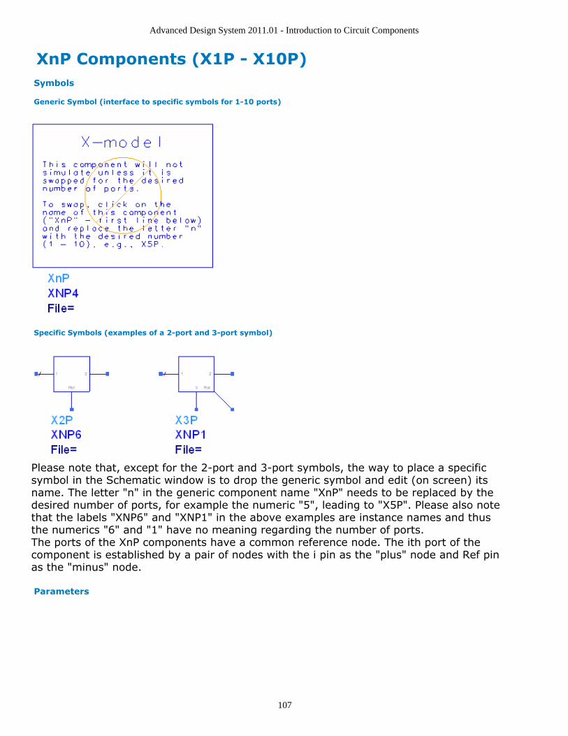
Advanced Design System 2011.01 - Introduction to Circuit Components
107
XnP Components (X1P - X10P) Symbols
Generic Symbol (interface to specific symbols for 1-10 ports)
Specific Symbols (examples of a 2-port and 3-port symbol)
Please note that, except for the 2-port and 3-port symbols, the way to place a specificsymbol in the Schematic window is to drop the generic symbol and edit (on screen) itsname. The letter "n" in the generic component name "XnP" needs to be replaced by thedesired number of ports, for example the numeric "5", leading to "X5P". Please also notethat the labels "XNP6" and "XNP1" in the above examples are instance names and thusthe numerics "6" and "1" have no meaning regarding the number of ports.The ports of the XnP components have a common reference node. The ith port of thecomponent is established by a pair of nodes with the i pin as the "plus" node and Ref pinas the "minus" node.
Parameters
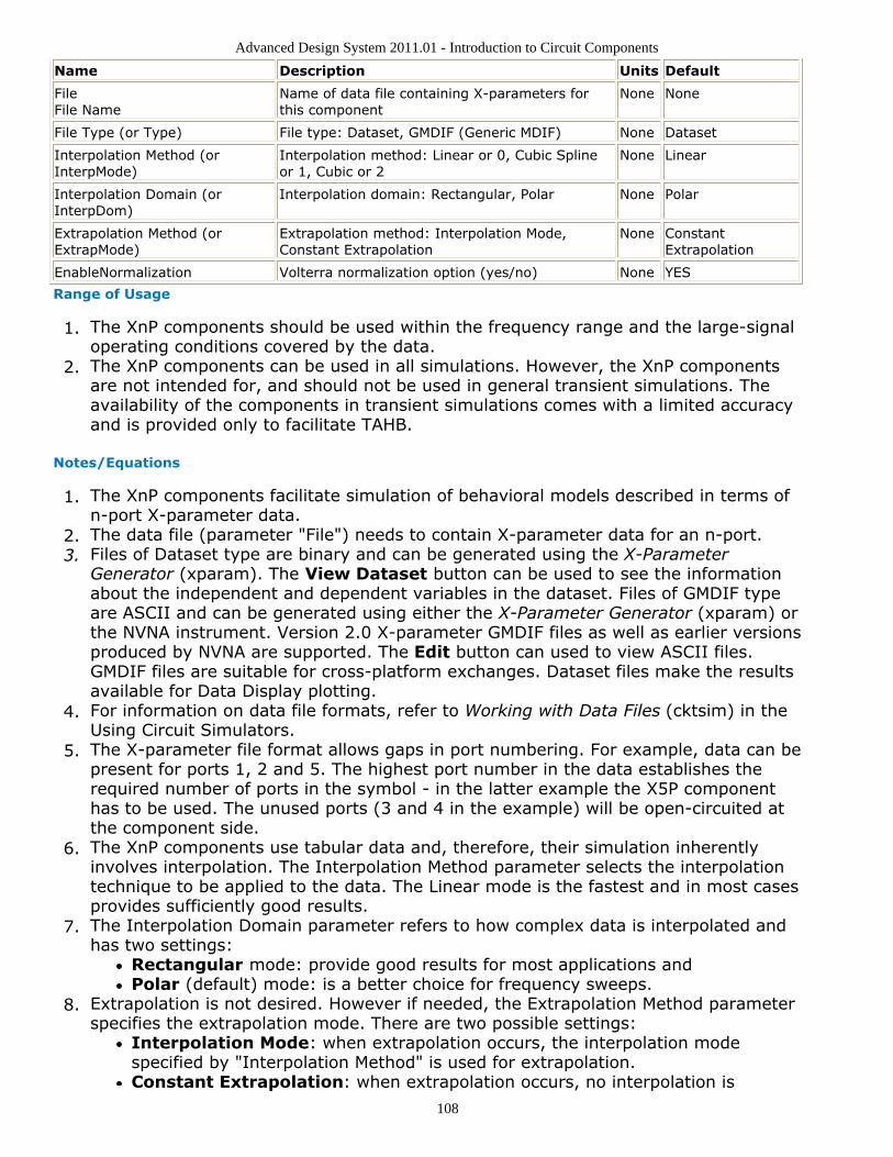
Advanced Design System 2011.01 - Introduction to Circuit Components
108
Name Description Units Default
FileFile Name
Name of data file containing X-parameters forthis component
None None
File Type (or Type) File type: Dataset, GMDIF (Generic MDIF) None Dataset
Interpolation Method (orInterpMode)
Interpolation method: Linear or 0, Cubic Splineor 1, Cubic or 2
None Linear
Interpolation Domain (orInterpDom)
Interpolation domain: Rectangular, Polar None Polar
Extrapolation Method (orExtrapMode)
Extrapolation method: Interpolation Mode,Constant Extrapolation
None ConstantExtrapolation
EnableNormalization Volterra normalization option (yes/no) None YES
Range of Usage
The XnP components should be used within the frequency range and the large-signal1.operating conditions covered by the data.The XnP components can be used in all simulations. However, the XnP components2.are not intended for, and should not be used in general transient simulations. Theavailability of the components in transient simulations comes with a limited accuracyand is provided only to facilitate TAHB.
Notes/Equations
The XnP components facilitate simulation of behavioral models described in terms of1.n-port X-parameter data.The data file (parameter "File") needs to contain X-parameter data for an n-port.2.Files of Dataset type are binary and can be generated using the X-Parameter3.Generator (xparam). The View Dataset button can be used to see the informationabout the independent and dependent variables in the dataset. Files of GMDIF typeare ASCII and can be generated using either the X-Parameter Generator (xparam) orthe NVNA instrument. Version 2.0 X-parameter GMDIF files as well as earlier versionsproduced by NVNA are supported. The Edit button can used to view ASCII files.GMDIF files are suitable for cross-platform exchanges. Dataset files make the resultsavailable for Data Display plotting.For information on data file formats, refer to Working with Data Files (cktsim) in the4.Using Circuit Simulators.The X-parameter file format allows gaps in port numbering. For example, data can be5.present for ports 1, 2 and 5. The highest port number in the data establishes therequired number of ports in the symbol - in the latter example the X5P componenthas to be used. The unused ports (3 and 4 in the example) will be open-circuited atthe component side.The XnP components use tabular data and, therefore, their simulation inherently6.involves interpolation. The Interpolation Method parameter selects the interpolationtechnique to be applied to the data. The Linear mode is the fastest and in most casesprovides sufficiently good results.The Interpolation Domain parameter refers to how complex data is interpolated and7.has two settings:
Rectangular mode: provide good results for most applications andPolar (default) mode: is a better choice for frequency sweeps.
Extrapolation is not desired. However if needed, the Extrapolation Method parameter8.specifies the extrapolation mode. There are two possible settings:
Interpolation Mode: when extrapolation occurs, the interpolation modespecified by "Interpolation Method" is used for extrapolation.Constant Extrapolation: when extrapolation occurs, no interpolation is
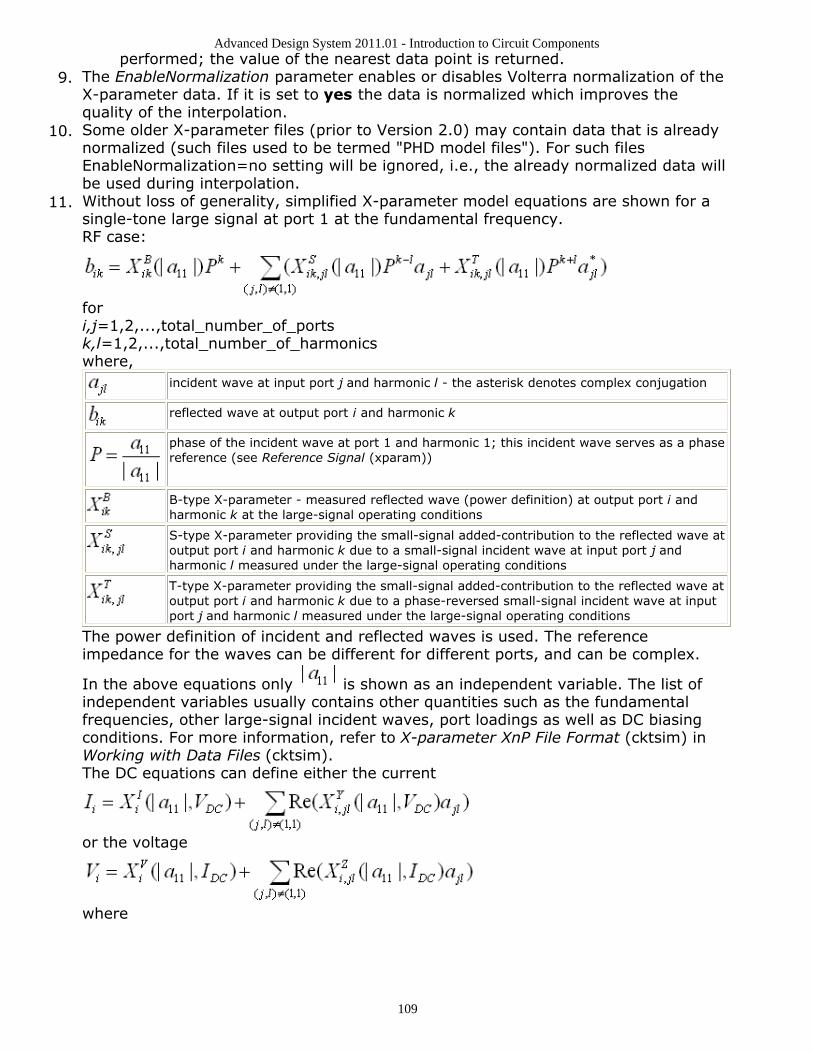
Advanced Design System 2011.01 - Introduction to Circuit Components
109
performed; the value of the nearest data point is returned.The EnableNormalization parameter enables or disables Volterra normalization of the9.X-parameter data. If it is set to yes the data is normalized which improves thequality of the interpolation.Some older X-parameter files (prior to Version 2.0) may contain data that is already10.normalized (such files used to be termed "PHD model files"). For such filesEnableNormalization=no setting will be ignored, i.e., the already normalized data willbe used during interpolation.Without loss of generality, simplified X-parameter model equations are shown for a11.single-tone large signal at port 1 at the fundamental frequency.RF case:
fori,j=1,2,...,total_number_of_portsk,l=1,2,...,total_number_of_harmonicswhere,
incident wave at input port j and harmonic l - the asterisk denotes complex conjugation
reflected wave at output port i and harmonic k
phase of the incident wave at port 1 and harmonic 1; this incident wave serves as a phasereference (see Reference Signal (xparam))
B-type X-parameter - measured reflected wave (power definition) at output port i andharmonic k at the large-signal operating conditions
S-type X-parameter providing the small-signal added-contribution to the reflected wave atoutput port i and harmonic k due to a small-signal incident wave at input port j andharmonic l measured under the large-signal operating conditions
T-type X-parameter providing the small-signal added-contribution to the reflected wave atoutput port i and harmonic k due to a phase-reversed small-signal incident wave at inputport j and harmonic l measured under the large-signal operating conditions
The power definition of incident and reflected waves is used. The referenceimpedance for the waves can be different for different ports, and can be complex.
In the above equations only is shown as an independent variable. The list ofindependent variables usually contains other quantities such as the fundamentalfrequencies, other large-signal incident waves, port loadings as well as DC biasingconditions. For more information, refer to X-parameter XnP File Format (cktsim) inWorking with Data Files (cktsim).The DC equations can define either the current
or the voltage
where
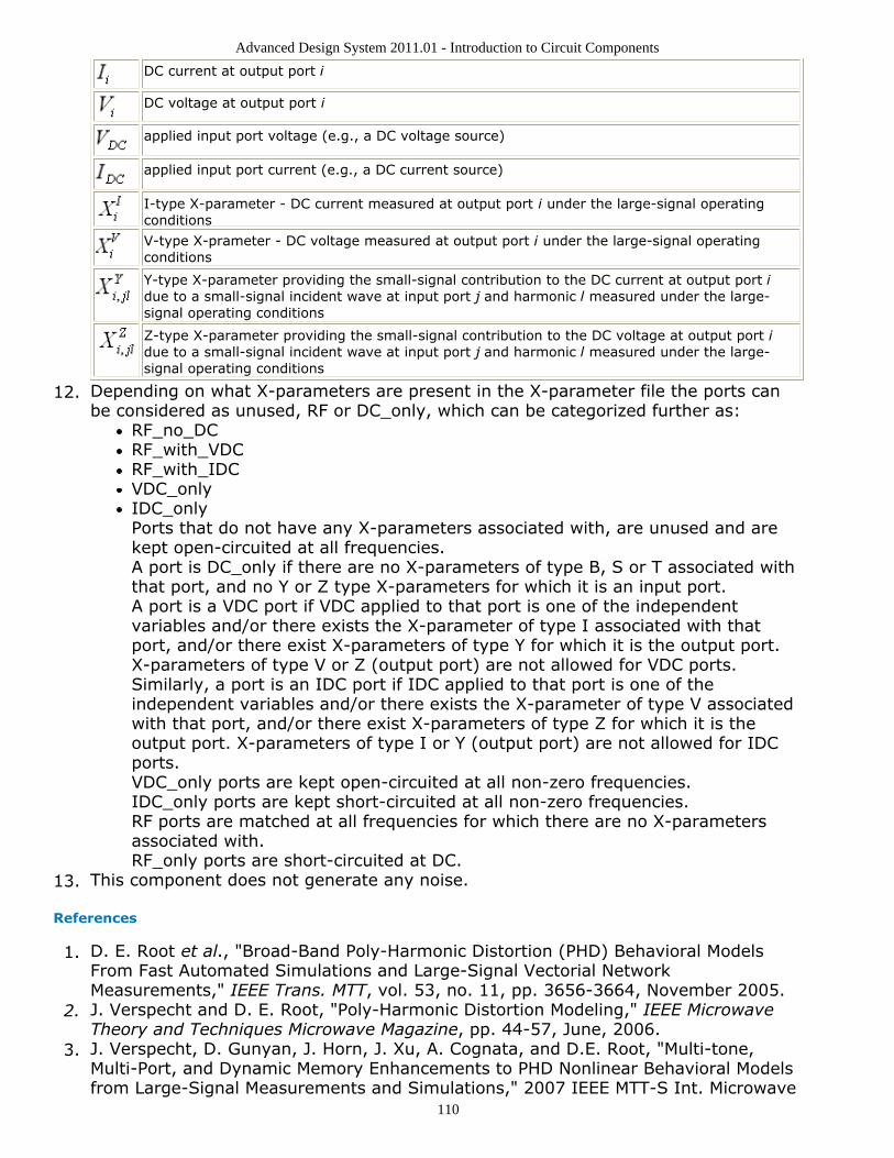
Advanced Design System 2011.01 - Introduction to Circuit Components
110
DC current at output port i
DC voltage at output port i
applied input port voltage (e.g., a DC voltage source)
applied input port current (e.g., a DC current source)
I-type X-parameter - DC current measured at output port i under the large-signal operatingconditions
V-type X-prameter - DC voltage measured at output port i under the large-signal operatingconditions
Y-type X-parameter providing the small-signal contribution to the DC current at output port idue to a small-signal incident wave at input port j and harmonic l measured under the large-signal operating conditions
Z-type X-parameter providing the small-signal contribution to the DC voltage at output port idue to a small-signal incident wave at input port j and harmonic l measured under the large-signal operating conditions
Depending on what X-parameters are present in the X-parameter file the ports can12.be considered as unused, RF or DC_only, which can be categorized further as:
RF_no_DCRF_with_VDCRF_with_IDCVDC_onlyIDC_onlyPorts that do not have any X-parameters associated with, are unused and arekept open-circuited at all frequencies.A port is DC_only if there are no X-parameters of type B, S or T associated withthat port, and no Y or Z type X-parameters for which it is an input port.A port is a VDC port if VDC applied to that port is one of the independentvariables and/or there exists the X-parameter of type I associated with thatport, and/or there exist X-parameters of type Y for which it is the output port.X-parameters of type V or Z (output port) are not allowed for VDC ports.Similarly, a port is an IDC port if IDC applied to that port is one of theindependent variables and/or there exists the X-parameter of type V associatedwith that port, and/or there exist X-parameters of type Z for which it is theoutput port. X-parameters of type I or Y (output port) are not allowed for IDCports.VDC_only ports are kept open-circuited at all non-zero frequencies.IDC_only ports are kept short-circuited at all non-zero frequencies.RF ports are matched at all frequencies for which there are no X-parametersassociated with.RF_only ports are short-circuited at DC.
This component does not generate any noise.13.
References
D. E. Root et al., "Broad-Band Poly-Harmonic Distortion (PHD) Behavioral Models1.From Fast Automated Simulations and Large-Signal Vectorial NetworkMeasurements," IEEE Trans. MTT, vol. 53, no. 11, pp. 3656-3664, November 2005.J. Verspecht and D. E. Root, "Poly-Harmonic Distortion Modeling," IEEE Microwave2.Theory and Techniques Microwave Magazine, pp. 44-57, June, 2006.J. Verspecht, D. Gunyan, J. Horn, J. Xu, A. Cognata, and D.E. Root, "Multi-tone,3.Multi-Port, and Dynamic Memory Enhancements to PHD Nonlinear Behavioral Modelsfrom Large-Signal Measurements and Simulations," 2007 IEEE MTT-S Int. Microwave

Advanced Design System 2011.01 - Introduction to Circuit Components
111
Symp. Dig., (Honolulu, HI), pp. 969-972, June 2007.J. Horn et al., "X-parameter Measurement and Simulation of a GSM Handset4.Amplifier", Proc. 3rd European Microwave Integrated Circuits Conf., (Amsterdam, TheNetherlands), pp. 135-138, October 2008.

Advanced Design System 2011.01 - Introduction to Circuit Components
112
Equation-Based Linear ComponentsChain (2-Port User-Defined Linear Chain) (ccsim)Hybrid (2-Port User-Defined Linear Hybrid) (ccsim)S1P Eqn to S6P Eqn (1- to 6-Port S-parameters, Equation-Based) (ccsim)Y1P Eqn to Y6P Eqn (1- to 6-Port Y-parameters, Equation-Based) (ccsim)Z1P Eqn to Z6P Eqn (1- to 6-Port Z-parameters, Equation-Based) (ccsim)

Advanced Design System 2011.01 - Introduction to Circuit Components
113
Chain (2-Port User-Defined Linear Chain)
Symbol
Parameters
Name Description Units Default
A Reverse voltage gain (v1/v2 with i2=0) None None
B Reverse transresistance (v1/i2 with v2=0) Ohm None
C Reverse transconductance (i1/v2 with i2=0) S None
D Reverse current gain (i1/i2 with v2=0) None None
ImpNoncausalLength Non-causal function impulse response order Integer None
ImpMode cOnvolution mode Integer None
ImpMax Freq Maximum frequency to which device is evaluated None
ImpDeltaFreq Sample spacing in frequency None
ImpMaxOrder Maximum impulse response order Integer None
ImpWindow Smoothing window Integer None
ImpRelTol Relative impulse response truncation factor None None
ImpAbsTol Absolute impulse response truncation factor None None
Notes/Equations
Port polarity is indicated by a minus (-) and a plus sign (+) on each port. Chain1.parameters are used when cascading a number of networks.Any chain parameter that is not defined initially is set to a default value of zero and2.cannot be modified later. Any chain parameter that is defined initially, even if it is setto zero, can be modified and swept. It can also be swept indirectly by sweeping avariable that it depends on. State current is available for port 2.Allowed values for ImpMode are 1 (Discrete) and 2 (PWL Continuous).3.Allowed values for ImpWindow are 0 (Rectangle) and 1 (Hanning).If these values are not specified, they default to the corresponding global parametervalues specified by the transient analysis controller item.Parameters A, B, C, and D can be made dependent on frequency by using the global4.variable freq.
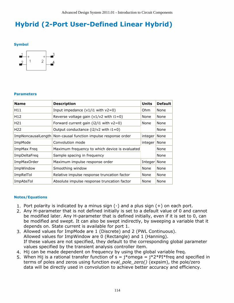
Advanced Design System 2011.01 - Introduction to Circuit Components
114
Hybrid (2-Port User-Defined Linear Hybrid)
Symbol
Parameters
Name Description Units Default
H11 Input impedance (v1/i1 with v2=0) Ohm None
H12 Reverse voltage gain (v1/v2 with i1=0) None None
H21 Forward current gain (i2/i1 with v2=0) None None
H22 Output conductance (i2/v2 with i1=0) None
ImpNoncausalLength Non-causal function impulse response order integer None
ImpMode Convolution mode integer None
ImpMax Freq Maximum frequency to which device is evaluated None
ImpDeltaFreq Sample spacing in frequency None
ImpMaxOrder Maximum impulse response order Integer None
ImpWindow Smoothing window None None
ImpRelTol Relative impulse response truncation factor None None
ImpAbsTol Absolute impulse response truncation factor None None
Notes/Equations
Port polarity is indicated by a minus sign (-) and a plus sign (+) on each port.1.Any H-parameter that is not defined initially is set to a default value of 0 and cannot2.be modified later. Any H-parameter that is defined initially, even if it is set to 0, canbe modified and swept. It can also be swept indirectly, by sweeping a variable that itdepends on. State current is available for port 1.Allowed values for ImpMode are 1 (Discrete) and 2 (PWL Continuous).3.Allowed values for ImpWindow are 0 (Rectangle) and 1 (Hanning).If these values are not specified, they default to the corresponding global parametervalues specified by the transient analysis controller item.Hij can be made dependent on frequency by using the global variable freq.4.When Hij is a rational transfer function of s = j*omega = j*2*PI*freq and specified in5.terms of poles and zeros using function eval_pole_zero() (expsim), the pole/zerodata will be directly used in convolution to achieve better accuracy and efficiency.

Advanced Design System 2011.01 - Introduction to Circuit Components
115
S1P_Eqn to S6P_Eqn (1- to 6-Port S-parameters,Equation-Based) Symbol
Parameters
Name Description Units Default
S[i, j] S-parameter in real and imaginary format None None
Z[i] Port i reference impedance None
NFmin Minimum noise figure (obsolete-not used) None None
Rn Noise resistance (obsolete-not used) None None
Sopt Optimum noise match (obsolete-not used) None None
Temp Device noise temperature °C
ImpNoncausalLength Non-causal function impulse response order Integer None
ImpMode Convolution mode Integer None
ImpMax Freq Maximum frequency to which device is evaluated None
ImpDeltaFreq Sample spacing in frequency None
ImpMaxOrder Maximum impulse response order Integer None
ImpWindow Smoothing window Integer None
ImpRelTol Relative impulse response truncation factor None None
ImpAbsTol Absolute impulse response truncation factor None None
Range of Usage
1 ≤ i, j ≤ port number
Notes/Equations
To enter a value for S[i,j], use the syntax a+j*b or complex (a,b). Expressions can1.be used as an entry, and the first syntax is in fact a special case with j being areserved symbol representing complex(0,1). Thus, the first syntax can be furthersimplified if either real or imaginary part is zero. For example, you can enter justS[1,1]=3 instead of S[1,1]=3+j*0. Also, subtraction, negative numbers andparentheses can be used as desired. The following four entries S[1,1]=0+j*2,S[1,1]=j*2, S[1,1]=0-j*(-2) S[1,1]=-j*(-2) are all supported and represent thesame value. Similarly, the entries S[1,1]=-j*j and S[1,1]=1.0 represent the same

Advanced Design System 2011.01 - Introduction to Circuit Components
116
value.If a value is not entered for S[i,j], it is set to a zero default value (0, 0) and cannot2.be modified later. If S[i,j] is initially defined (even as zero), it can be modified andswept. It can also be swept indirectly, by sweeping a variable that it depends on.State currents are available for the port.Port polarity is indicated by a minus (-) and a plus sign (+) on each port. The port3.can be made reciprocal by setting Recip=YES. By declaring the device to bereciprocal, S[i,j]] is always forced to equal S[j,i]. Only one of the two can be defined.If NFmin, Sopt, and Rn are used to characterize noise in S2P_Eqn, the following4.relation must be satisfied for a realistic model.
A warning message will be issued if Rn does not meet this criterion. If the noiseparameters attempt to describe a system that requires negative noise (due to Rnbeing too small), the negative part of the noise will be set to zero and a warningmessage will be issued.If the component temperature Temp is < -273°C, the component does not generate5.any noise. For S2P_Eqn only, if noisy 2-port parameters (minimum noise figureNFmin, optimum source reflection coefficient Sopt and effective noise sourceresistance Rn) are specified, these parameters are used to calculate the device'snoise performance, independent of Temp. If the S-parameters describe a passivedevice, Temp and Twiss's theorem are used to calculate noise performance; if the S-parameters describe an active device, (i.e., the S-parameters are not passive), non-real noise is generated resulting in meaningless noise data. Further, if the network isnot passive, a warning is issued to the Simulation Status window.Allowed values for ImpMode are 1 (Discrete) and 2 (PWL Continuous).6.Allowed values for ImpWindow are 0 (Rectangle) and 1 (Hanning).If these values are not specified, they default to the corresponding global parametervalues specified by the transient analysis controller item.S[i,j] can be made dependent on frequency by using the global variable freq. For7.example, you can use a brick wall lowpass filter by using S21=if(freq<1 GHz), then 1else 0.

Advanced Design System 2011.01 - Introduction to Circuit Components
117
Y1P_Eqn to Y6P_Eqn (1- to 6-Port Y-parameters,Equation-Based) Symbol
Parameters
Name Description Units Default
Y[i,j] Y-parameter in real and imaginary format
Temp Temperature °C
ImpNoncausalLength Non-causal function impulse response order Integer None
ImpMode Convolution mode Integer None
ImpMax Freq Maximum frequency to which device is evaluated None
ImpDeltaFreq Sample spacing in frequency None
ImpMaxOrder Maximum impulse response order Integer None
ImpWindow Smoothing window Integer None
ImpRelTol Relative impulse response truncation factor None None
ImpAbsTol Absolute impulse response truncation factor None None
Range of Usage
1 ≤ i, j ≤ port number
Notes/Equations
To enter a value for Y[i,j], use the syntax a+j*b or complex (a,b). Expressions can1.be used as an entry, and the first syntax is in fact a special case with j being areserved symbol representing complex(0,1). Thus, the first syntax can be furthersimplified if either real or imaginary part is zero. For example, you can enter justY[1,1]=3 instead of Y[1,1]=3+j*0. Also, subtraction, negative numbers andparentheses can be used as desired. The following four entries Y[1,1]=0+j*2,Y[1,1]=j*2, Y[1,1]=0-j*(-2) Y[1,1]=-j*(-2) are all supported and represent the samevalue. Similarly, the entries Y[1,1]=-j*j and Y[1,1]=1.0 represent the same value.If a value is not entered for Y[i,j], it is set to a zero default value (0, 0) and cannot2.be modified later. If Y[i,j] is initially defined (even as zero), it can be modified andswept. It can also be swept indirectly, by sweeping a variable that it depends on.State currents are available for the port.

Advanced Design System 2011.01 - Introduction to Circuit Components
118
Port polarity is indicated by a minus (-) and a plus sign (+) on each port. The port3.can be made reciprocal by setting Recip=YES. By declaring the device to bereciprocal, Y[i,j]] is always forced to equal Y[j,i]. Only one of the two can be defined.Allowed values for ImpMode are 1 (Discrete) and 2 (PWL Continuous).4.Allowed values for ImpWindow are 0 (Rectangle) and 1 (Hanning).If ImpMode, ImpMaxFreq, or ImpMaxOrder are not specified, they default to theglobal ImpMode specified by the transient analysis controller item.Y[i,j] can be made dependent on frequency by using the global variable freq.5.When Y[i,j] is a rational transfer function of s = j*omega = j*2*PI*freq and specified6.in terms of poles and zeros using function eval_pole_zero() (expsim), the pole/zerodata will be directly used in convolution to achieve better accuracy and efficiency.

Advanced Design System 2011.01 - Introduction to Circuit Components
119
Z1P_Eqn to Z6P_Eqn (1- to 6-Port Z-parameters,Equation-Based) Symbol
Parameters
Name Description Units Default
Z[i,j] Z-parameter in real and imaginary format None None
C[i] Port 1 controlling current (refer to Notes) None None
Temp Temperature °C
ImpNoncausalLength Non-causal function impulse response order Integer None
ImpMode Convolution mode Integer None
ImpMax Freq Maximum frequency to which device is evaluated None
ImpDeltaFreq Sample spacing in frequency None
ImpMaxOrder Maximum impulse response order Integer None
ImpWindow Smoothing window Integer None
ImpRelTol Relative impulse response truncation factor None None
ImpAbsTol Absolute impulse response truncation factor None None
Range of Usage
1 ≤ i, j ≤ port number
Notes/Equations
To enter a value for Z[i,j], use the syntax a+j*b or complex (a,b). Expressions can1.be used as an entry, and the first syntax is in fact a special case with j being areserved symbol representing complex(0,1). Thus, the first syntax can be furthersimplified if either real or imaginary part is zero. For example, you can enter justZ[1,1]=3 instead of Z[1,1]=3+j*0. Also, subtraction, negative numbers andparentheses can be used as desired. The following four entries Z[1,1]=0+j*2,Z[1,1]=j*2, Z[1,1]=0-j*(-2) Z[1,1]=-j*(-2) are all supported and represent thesame value. Similarly, the entries Z[1,1]=-j*j and Z[1,1]=1.0 represent the samevalue.If a value is not entered for Z[i,j], it is set to a zero default value (0, 0) and cannot2.be modified later. If Z[i,j] is initially defined (even as zero), it can be modified and
Advanced Design System 2011.01 - Introduction to Circuit Components
120
swept. It can also be swept indirectly, by sweeping a variable that it depends on.State currents are available for the port.Port polarity is indicated by a minus (-) and a plus sign (+) on each port. The port3.can be made reciprocal by setting Recip=YES. By declaring the device to bereciprocal, Z[i,j]] is always forced to equal Z[j,i]. Only one of the two can be defined.Allowed values for ImpMode are 1 (Discrete) and 2 (PWL Continuous).4.Allowed values for ImpWindow are 0 (Rectangle) and 1 (Hanning).If these values are not specified, they default to the corresponding global parametervalues specified by the transient analysis controller item.The C[i] parameter can be used to model the mutual coupling between ZnP_Eqn and5.other components in the circuit. For example, Z1P_Eqn_A is used to model a one-port block and Z1P_Eqn_B is used to model another one-port block. C[1] can be usedto model the mutual coupling between Z1P_Eqn_A and Z1P_Eqn_B.Z[i,j] can be made dependent on frequency by using the global variable freq.6.
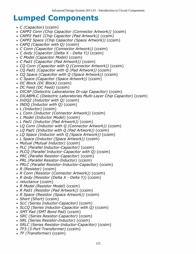
Advanced Design System 2011.01 - Introduction to Circuit Components
121
Lumped ComponentsC (Capacitor) (ccsim)CAPP2 Conn (Chip Capacitor (Connector Artwork)) (ccsim)CAPP2 Pad1 (Chip Capacitor (Pad Artwork)) (ccsim)CAPP2 Space (Chip Capacitor (Space Artwork)) (ccsim)CAPQ (Capacitor with Q) (ccsim)C Conn (Capacitor (Connector Artwork)) (ccsim)C dxdy (Capacitor (Delta X - Delta Y)) (ccsim)C Model (Capacitor Model) (ccsim)C Pad1 (Capacitor (Pad Artwork)) (ccsim)CQ Conn (Capacitor with Q (Connector Artwork)) (ccsim)CQ Pad1 (Capacitor with Q (Pad Artwork)) (ccsim)CQ Space (Capacitor with Q (Space Artwork)) (ccsim)C Space (Capacitor (Space Artwork)) (ccsim)DC Block (DC Block) (ccsim)DC Feed (DC Feed) (ccsim)DICAP (Dielectric Laboratories Di-cap Capacitor) (ccsim)DILABMLC (Dielectric Laboratories Multi-Layer Chip Capacitor) (ccsim)InDQ2 (Inductor with Q) (ccsim)INDQ (Inductor with Q) (ccsim)L (Inductor) (ccsim)L Conn (Inductor (Connector Artwork)) (ccsim)L Model (Inductor Model) (ccsim)L Pad1 (Inductor (Pad Artwork)) (ccsim)LQ Conn (Inductor with Q (Connector Artwork)) (ccsim)LQ Pad1 (Inductor with Q (Pad Artwork)) (ccsim)LQ Space (Inductor with Q (Space Artwork)) (ccsim)L Space (Inductor (Space Artwork)) (ccsim)Mutual (Mutual Inductor) (ccsim)PLC (Parallel Inductor-Capacitor) (ccsim)PLCQ (Parallel Inductor-Capacitor with Q) (ccsim)PRC (Parallel Resistor-Capacitor) (ccsim)PRL (Parallel Resistor-Inductor) (ccsim)PRLC (Parallel Resistor-Inductor-Capacitor) (ccsim)R (Resistor) (ccsim)R Conn (Resistor (Connector Artwork)) (ccsim)R dxdy (Resistor (Delta X - Delta Y)) (ccsim)reluctance (ccsim)R Model (Resistor Model) (ccsim)R Pad1 (Resistor (Pad Artwork)) (ccsim)R Space (Resistor (Space Artwork)) (ccsim)Short (Short) (ccsim)SLC (Series Inductor-Capacitor) (ccsim)SLCQ (Series Inductor-Capacitor with Q) (ccsim)SMT Pad (SMT Bond Pad) (ccsim)SRC (Series Resistor-Capacitor) (ccsim)SRL (Series Resistor-Inductor) (ccsim)SRLC (Series Resistor-Inductor-Capacitor) (ccsim)TF3 (3-Port Transformer) (ccsim)TF (Transformer) (ccsim)

Advanced Design System 2011.01 - Introduction to Circuit Components
122

Advanced Design System 2011.01 - Introduction to Circuit Components
123
C (Capacitor)
Symbol
Parameters
Name Description Units Default
C Capacitance pF 1.0
Temp Temperature °C None
Trise Temperature rise over ambient °C None
Tnom Nominal temperature °C 25
TC1 Temperature coefficient; per degree Celsius 1/°C None
TC2 Temperature coefficient; per degree Celsius squared 1/°C2 None
wBV Breakdown voltage warning None
InitCond Initial condition for transient analysis None None
Model Name of a capacitor model to use None None
Width Physical width for use with a model None
Length Physical length for use with a model None
_M Number of capacitors in parallel None 1
Notes/Equations
The capacitor value can be made a function of temperature by setting Tnom and1.either TC1 or TC2 or both. Tnom specifies the nominal temperature at which C isgiven. Tnom defaults to 25°C. If Temp≠Tnom, then the simulated capacitance valueis given by:
If Temp is not explicitly specified, it defaults to the global temperature specified in2.the options item.wBV is used by the overload alert feature. It sets a limit on the maximum voltage3.across the capacitor. If this limit is specified, the simulator will issue a warning thefirst time it is exceeded during a dc, harmonic balance or transient simulation.Simulation results are not affected by this parameter.If a model name is given, then values that are not specified on the capacitor instance4.are taken from the model values. Typical values that can be defaulted arecapacitance, length and width, nominal temperature, temperature coefficients, andoverload alert parameters.If a model is used, the capacitance value to be simulated (before temperature scalingis applied) is calculated as:

Advanced Design System 2011.01 - Introduction to Circuit Components
124
_M is used to represent the number of capacitors in parallel and defaults to 1. If a5.capacitor model is used, an optional scaling parameter Scale can also be defined onthe model; it defaults to 1. The effective capacitance that will be simulated isC × Scale × M.When InitCond is explicitly specified, the check-box Use user-specified initial6.conditions must be turned on in the Convergence tab of the Tran transient simulationcontroller for the parameter setting to take effect.The postive polarity of the initial conditions is applied to pin 1 (reference capacitor7.symbol above), therefore the terminal with the curved line is positive for a positivevoltage.DC Operating Point Information lists the DC operating point parameters that can be8.sent to the dataset.
DC Operating Point Information
Name Description Units
C Capacitance F

Advanced Design System 2011.01 - Introduction to Circuit Components
125
CAPP2_Conn (Chip Capacitor (Connector Artwork)) Symbol
Parameters
Name Description Units Default
C Capacitance pF 1.0
TanD Dielectric loss tangent None 0.001
Q Quality factor None 50.0
FreQ Resistance frequency for Q MHz 300.0
FreqRes Resistance frequency MHz 500.0
Exp Exponent for frequency dependence ofQ
None 2.0
Temp Temperature °C 25
Range of Usage
C, Q, FreqQ, FreqRes ≥ 0
Notes/Equations
The series resistance Rs is determined by the Q and the parallel resistance Rp is1.determined by TanD.The frequency-dependence of Q is given byQ (f) = Q (FQ) (FreqQ/f)Expwhere f is the simulation frequency and Q(FreqQ) is the specified value of Q atFreqQ.If Q or FreqQ are set to 0, Q is assumed to be infinite.2.For time-domain analysis, the frequency-domain analytical model is used.3.This component has no default artwork associated with it.4.
References
C. Bowick, RF Circuit Design, Howard Sams & Co., 1987.1.The RF Capacitor Handbook, American Technical Ceramics Corp., September 1983.2.
Equivalent Circuit

Advanced Design System 2011.01 - Introduction to Circuit Components
126
CAPP2_Pad1 (Chip Capacitor (Pad Artwork)) Symbol
Parameters
Name Description Units Default
C Capacitance pF 1.0
TanD Dielectric loss tangent None 0.001
Q Quality factor None 50.0
FreqQ Resistance frequency for Q MHz 300.0
FreqRes Resonance frequency MHz 500.0
Exp Exponent for frequency dependence ofQ
None 2.0
W (ADS Layout option) Width of pad mil 25.0
S (ADS Layout option) Spacing mil 10.0
L1 (ADS Layout option) Pin-to-pin distance mil 50.0
Temp Temperature °C 25
Range of Usage
C, Q, FreqQ, FreqRes ≥ 0
Notes/Equations
The series resistance Rs is determined by the Q and the parallel resistance Rp is1.determined by TanD.The frequency-dependence of Q is given byQ (f) = Q (FreqQ) (FreqQ/f)Expwhere f is the simulation frequency and Q(FreqQ) is the specified value of Q atFreqQ.If Q or FreqQ are set to 0, Q is assumed to be infinite.2.For time-domain analysis, the frequency-domain analytical model is used.3.This component's artwork is composed of two rectangular pads with pins on the outer4.edges.
References
Bowick, Cris. RF Circuit Design, Howard Sams & Co., 1987.1.

Advanced Design System 2011.01 - Introduction to Circuit Components
127
The RF Capacitor Handbook, American Technical Ceramics Corp., September 1983.2.
Equivalent Circuit

Advanced Design System 2011.01 - Introduction to Circuit Components
128
CAPP2_Space (Chip Capacitor (Space Artwork)) Symbol
Parameters
Name Description Units Default
C Capacitance pF 1.0
TanD Dielectric loss tangent None 0.001
Q Quality factor None 50.0
FreQ Resistance frequency for Q MHz 300.0
FreqRes Resistance frequency MHz 500.0
Exp Exponent for frequency dependence ofQ
None 2.0
L1 (ADS Layout option) Pin-to-pin distance mil 50.0
Temp Temperature °C 25
Range of Usage
C, Q, FreqQ, FR ≥ 0
Notes/Equations
The series resistance Rs is determined by the Q and the parallel resistance Rp is1.determined by TanD.The frequency-dependence of Q is given byQ (f) = Q (FreqQ) (FreqQ/f)Expwhere f is the simulation frequency and Q(FreqQ) is the specified value of Q atFreqQ.If Q or FreqQ are set to 0, Q is assumed to be infinite.2.For time-domain analysis, the frequency-domain analytical model is used.3.This component is represented as a connected gap in layout into which a custom4.artwork object can be inserted.
References
C. Bowick, RF Circuit Design, Howard Sams & Co., 1987.1.The RF Capacitor Handbook, American Technical Ceramics Corp., September 1983.2.
Equivalent Circuit

Advanced Design System 2011.01 - Introduction to Circuit Components
129
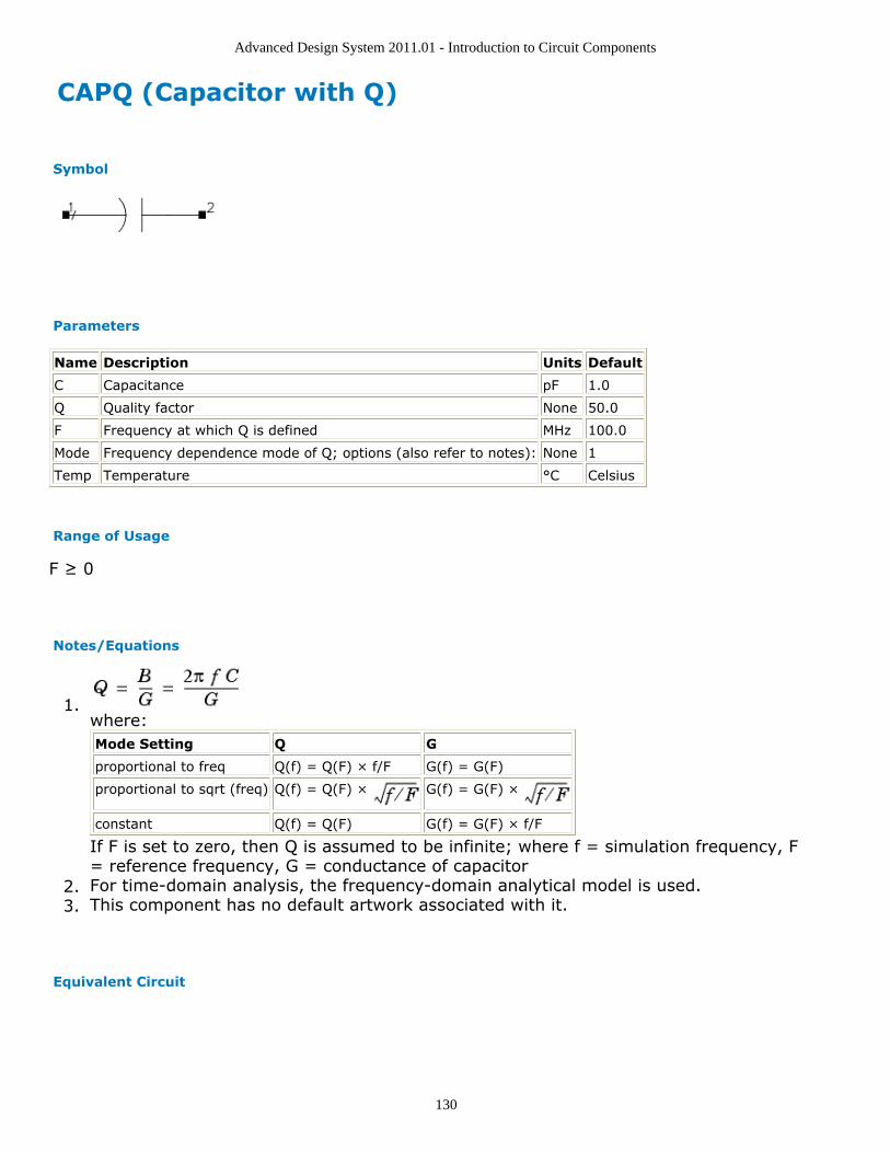
Advanced Design System 2011.01 - Introduction to Circuit Components
130
CAPQ (Capacitor with Q)
Symbol
Parameters
Name Description Units Default
C Capacitance pF 1.0
Q Quality factor None 50.0
F Frequency at which Q is defined MHz 100.0
Mode Frequency dependence mode of Q; options (also refer to notes): None 1
Temp Temperature °C Celsius
Range of Usage
F ≥ 0
Notes/Equations
1.where:Mode Setting Q G
proportional to freq Q(f) = Q(F) × f/F G(f) = G(F)
proportional to sqrt (freq) Q(f) = Q(F) × G(f) = G(F) ×
constant Q(f) = Q(F) G(f) = G(F) × f/F
If F is set to zero, then Q is assumed to be infinite; where f = simulation frequency, F= reference frequency, G = conductance of capacitorFor time-domain analysis, the frequency-domain analytical model is used.2.This component has no default artwork associated with it.3.
Equivalent Circuit

Advanced Design System 2011.01 - Introduction to Circuit Components
131

Advanced Design System 2011.01 - Introduction to Circuit Components
132
C_Conn (Capacitor (Connector Artwork)) Symbol
Parameters
Name Description Units Default
C Capacitance pF 1.0
Notes/Equations
This component is a single connection in layout. For example, it can be used to1.represent parasitics.
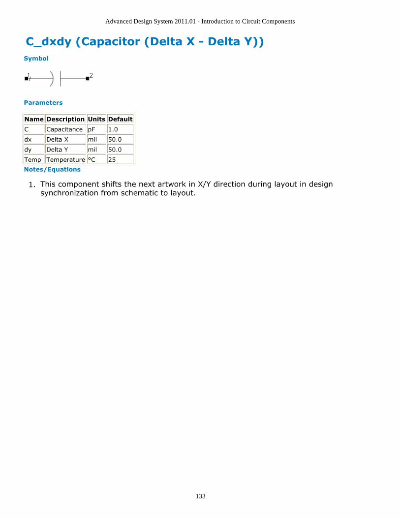
Advanced Design System 2011.01 - Introduction to Circuit Components
133
C_dxdy (Capacitor (Delta X - Delta Y)) Symbol
Parameters
Name Description Units Default
C Capacitance pF 1.0
dx Delta X mil 50.0
dy Delta Y mil 50.0
Temp Temperature °C 25
Notes/Equations
This component shifts the next artwork in X/Y direction during layout in design1.synchronization from schematic to layout.

Advanced Design System 2011.01 - Introduction to Circuit Components
134
C_Model (Capacitor Model)
Symbol
Parameters
Name Description Units Default
C (Cap) Capacitance pF 1.0
Cj Capacitance per area None
Cjsw (Capsw) Sidewall or periphery capacitance None
Length (L) † Length None
Width (W) † Width None
Narrow (Etch) Length and width narrowing due to etching None
Tnom Nominal temperature °C 25
Trise Temperature rise over ambient °C None
TC1 Temperature coefficient; per degree Celsius 1/°C None
TC2 Temperature coefficient; per degree Celsius squared 1/°C2 None
wBV Breakdown voltage (warning) None
Scale (Scalec) Capacitance scaling factor None 1
Coeffs Nonlinear capacitor polynomial coefficients (syntax:list(c1,c2,...))
None None
AllParams Data Access Component (DAC) Based Parameters None None
† Each instance parameter whose dimension contains a power of meter will be multiplied by the Scale tothe same power. For example, a parameter with a dimension of m will be multiplied by scale1 and aparameter with a dimension of m2 will be multiplied by scale2 . Note that only parameters whose dimensionscontain meter are scaled. For example, a parameter whose dimension contains cm instead of meter is notscaled.
Netlist Format
Model statements for the ADS circuit simulator may be stored in an external file. This istypically done with foundry model kits. For more information on how to set up and usefoundry model kits, refer to Design Kit Development (dkarch).
model modelname C_Model [parm=value]*
The model statement starts with the required keyword model . It is followed by themodelname that will be used by capacitor components to refer to the model. The thirdparameter indicates the type of model; for this model it is _C_Model_ . The rest of the

Advanced Design System 2011.01 - Introduction to Circuit Components
135
model contains pairs of model parameters and values, separated by an equal sign. Thename of the model parameter must appear exactly as shown in the parameters table-these names are case sensitive. Some model parameters have aliases, which are listed inparentheses after the main parameter name; these are parameter names that can beused instead of the primary parameter name. Model parameters may appear in any orderin the model statement. Model parameters that are not specified take the default valueindicated in the parameters table. For more information about the ADS circuit simulatornetlist format, refer to ADS Simulator Input Syntax (cktsim).Example:
model mimCap C_Model \
Cje=1e-3 Cjsw=1e-10 Tc1=-1e-3 \
Coeffs=list(1,2)
Notes/Equations
This model supplies values for a capacitor C. This allows physically-based capacitors1.to be modeled based on length and width.Use AllParams with a DataAccessComponent to specify file-based parameters (refer2.to DataAccessComponent). Note that model parameters that are explicitly specifiedtake precedence over those specified via AllParams.The capacitor value can be made a nonlinear function of the applied voltage V by3.specifying the polynomial coefficients list (Coeffs = list(c1, c2, c3, ...) ). Thecapacitance value C ( V ) is then given by:
where C is the capacitance of the instance, and ck is the k -th entry in the Coeffs list.If C for the instance is not given, C for the model will be used.The charge as a function of the applied voltage is:
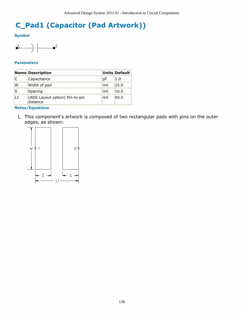
Advanced Design System 2011.01 - Introduction to Circuit Components
136
C_Pad1 (Capacitor (Pad Artwork)) Symbol
Parameters
Name Description Units Default
C Capacitance pF 1.0
W Width of pad mil 25.0
S Spacing mil 10.0
L1 (ADS Layout option) Pin-to-pindistance
mil 50.0
Notes/Equations
This component's artwork is composed of two rectangular pads with pins on the outer1.edges, as shown:

Advanced Design System 2011.01 - Introduction to Circuit Components
137
CQ_Conn (Capacitor with Q (Connector Artwork)) Symbol
Parameters
Name Description Units Default
C Capacitance pF 1.0
Q Quality factor None 50.0
F Frequency at which Q is defined MHz 100.0
Mode Frequency dependence mode of Q; options (also refer to notes): 1=proportional tofreq 2=proportional to sqrt(freq) 3=constant
None 1
Temp Temperature °C 25
Range of Usage
F ≥ 0
Notes/Equations
1.where:Mode Setting Q G
proportional to freq Q(f) = Q(F) f/F G(f) = G(F)
proportional to sqrt (freq) Q(f) = Q(F) G(f) = G(F)
constant Q(f) = Q(F) G(f) = G(F) f/F
If F is set to zero, then Q is assumed to be infinitewhere, f = simulation frequencyF = reference frequencyG = conductance of capacitorFor time-domain analysis, the frequency-domain analytical model is used.2.This component is a single connection in layout. For example, it can be used to3.represent parasitics.
Equivalent Circuit

Advanced Design System 2011.01 - Introduction to Circuit Components
138
CQ_Pad1 (Capacitor with Q (Pad Artwork)) Symbol
Parameters
Name Description Units Default
C Capacitance pF 1.0
Q Quality factor None 50.0
F Frequency at which Q is defined MHz 100.0
Mode Frequency dependence mode of Q; options (also refer to notes):
1=proportional to freq2=proportional to sqrt(freq)3=constant
None 1
W (ADS Layout option) Width of pad mil 25.0
S (ADS Layout option) Spacing mil 10.0
L1 (ADS Layout option) Pin-to-pin distance mil 50.0
Temp Temperature °C 25
Range of Usage
F ≥ 0
Notes/Equations
1.where:Mode Setting Q G
proportional to freq Q(f) = Q(F) f/F G(f) = G(F)
proportional to sqrt (freq) Q(f) = Q(F) G(f) = G(F)
constant Q(f) = Q(F) G(f) = G(F) f/F
If F is set to zero, then Q is assumed to be infinite. where f = simulation frequencyF = reference frequencyG = conductance of capacitorFor time-domain analysis, the frequency-domain analytical model is used.2.This component's artwork is composed of two rectangular pads with pins on the outer3.edges, as shown:

Advanced Design System 2011.01 - Introduction to Circuit Components
139
Equivalent Circuit

Advanced Design System 2011.01 - Introduction to Circuit Components
140
CQ_Space (Capacitor with Q (Space Artwork)) Symbol
Parameters
Name Description Units Default
C Capacitance pF 1.0
Q Quality factor None 50.0
F Frequency at which Q is defined MHz 100.0
Mode Frequency dependence mode of Q; options (also refer to notes):
1=proportional to freq2=proportional to sqrt(freq)3=constant
None 1
L1 (ADS Layout option) Pin-to-pin distance mil 50.0
Temp Temperature °C 25
Range of Usage
F ≥ 0
Notes/Equations
1.where:Mode Setting Q G
proportional to freq Q(f) = Q(F) f/F G(f) = G(F)
proportional to sqrt (freq) Q(f) = Q(F) G(f) = G(F)
constant Q(f) = Q(F) G(f) = G(F) f/F
If F is set to zero, then Q is assumed to be infinite. where f = simulation frequencyF = reference frequencyG = conductance of capacitorFor time-domain analysis, the frequency-domain analytical model is used.2.This component is represented as a connected gap in layout---into which a custom3.artwork object can be inserted.
Equivalent Circuit

Advanced Design System 2011.01 - Introduction to Circuit Components
141

Advanced Design System 2011.01 - Introduction to Circuit Components
142
C_Space (Capacitor (Space Artwork)) Symbol
Parameters
Name Description Units Default
C Capacitance pF 1.0
L1 (ADS Layout option) Pin-to-pindistance
mil 50.0
Notes/Equations
This component is represented as a connected gap in layout into which a custom1.artwork object can be inserted.

Advanced Design System 2011.01 - Introduction to Circuit Components
143
DC_Block (DC Block)
Symbol
Parameters
Name Description Units Default
Mode Integer values denote functionality:-1=blocks AC but feeds DC0=feeds both AC andDC1=blocks DC but feeds AC
Integer 1 †
C DC block capacitance None
L DC feed inductance None
Gain Current gain None None
wImax Maximum current (warning) None
† Refer to DC_Feed and Short components for other default settings.
Notes/Equations
The C and L parameters are used for transient simulation only because open for1.DC_Block is non-causal for Transient simulation.The dc block in Transient is not an infinite C; it defaults to 1 µf.Reasonable C and L values (especially for Transient and Circuit Envelope simulation)are strongly recommended wherever possible.

Advanced Design System 2011.01 - Introduction to Circuit Components
144
DC_Feed (DC Feed)
Symbol
Parameters
Name Description Units Default
Mode Integer values denote functionality:-1=blocks AC but feeds DC0=feeds both AC andDC1=blocks DC but feeds AC
None -1 †
C DC block capacitance None
L DC feed inductance None
Gain Current gain None None
wImax Maximum current (warning) None
† Refer to DC_Block and Short components for other default settings.
Notes/Equations
The C and L parameters are used for transient simulation only because short for1.DC_Feed is non-causal for transient simulation.

Advanced Design System 2011.01 - Introduction to Circuit Components
145
DICAP (Dielectric Laboratories Di-cap Capacitor) Symbol
Illustration
Parameters
Name Description Units Default
W Width of metal plates and dielectric mil 25.0
L Length of metal plates and dielectric mil 25.0
T Thickness of dielectric mil 4.0
Er Dielectric constant None 2.50
TanDeL Dielectric loss tangent value at 1 MHz None 0.001
R0 Series resistance at 1 GHz Ohm 0.01
Cond1_Layer (for Layout option) Layer on which the bottom plate is drawn select from layeroptions
cond
Diel_Layer (for Layout option) Layer on which the dielectric is drawn select from layeroptions
diel
Cond2_Layer (for Layout option) Layer on which the airbridge is drawn select from layeroptions
cond2
Temp Temperature °C 25
Notes/Equations
This is the Di-cap capacitor model by Dielectric Laboratories Incorporated; for the1.parameter values, please contact Dielectric Laboratories.DICAP is a single-layer capacitor that behaves as lossy parallel plate transmission2.lines. Pin 1 is on the bottom metal plate; pin 2 is on the top metal plate. Theconnection (such as Wire or Ribbon) from the top metal plate (pin 2) to theconnecting transmission line is not included in the model---the user must connect itseparately.For time-domain analysis, the frequency-domain analytical model is used.3.In the layout, the top metal will be drawn on layer cond2; the bottom metal on layer4.cond; and, the capacitor dielectric on layer diel.

Advanced Design System 2011.01 - Introduction to Circuit Components
146
DILABMLC (Dielectric Laboratories Multi-Layer ChipCapacitor) Symbol
Illustration
Parameters
Name Description Units Default
C0 Nominal capacitance pF 1.0
TanDel Dielectric loss tangent value at 1 MHz None 0.001
RO Bulk resistivity of termination at 1 MHz Ohm 0.01
Rt Termination loss resistance at 1 MHz Ohm 0.01
Re Electrode loss resistance per electrode at 1 GHz Ohm 0.01
Mount Mounting orientation: flat or edge None flat
W Width of dielectric mil 30.0
L Length of dielectric mil 60.0
H Height of dielectric mil 30.0
Cond1_Layer (for Layout option) Layer on which the bottom plate is drawn select from layeroptions
cond
Diel_Layer (for Layout option) Layer on which the dielectric is drawn select from layeroptions
diel
Cond2_Layer (for Layout option) Layer on which the airbridge is drawn select from layeroptions
cond2
Temp Temperature °C 25
Notes/Equations
This is the multi-layer chip capacitor model by Dielectric Laboratories Incorporated;1.for the parameter values, please contact Dielectric Laboratories.DILABMLC behaves as an open-ended transmission line. Pins 1 and 2 are at the2.edges of the capacitor's solder leads. The connections (such as Wire or Ribbon) fromthe solder leads to the connecting transmission line are not included in the model---the user must connect them separately.For transient analysis, the DILABMLC is modelled as a series RLC equivalent circuit.3.

Advanced Design System 2011.01 - Introduction to Circuit Components
147
For convolution analysis, the frequency domain analytical model is used.4.Attention should be given on the mounting orientation of the DILABMLC capacitor5.(whether it is flat or edge-mounted). The orientation of the capacitor relative to thegap in the microstrip affects the sequence of resonances.When the internal electrodes are parallel to the plane of the microstrip (flat mounted)parallel resonances occur when the equivalent line length is either an even or oddmultiple of a half wave-length.When the internal electrodes are normal to the substrate (edge mounted),resonances occur only when the multiple is even. This suppression of odd-orderedresonances it the result of exciting the equivalent line at its center rather than at oneend. Consequently, resonance occurs at higher frequencies when edge mounted.

Advanced Design System 2011.01 - Introduction to Circuit Components
148
InDQ2 (Inductor with Q)
Symbol
Parameters
Name Description Units Default
L Inductance nH 1.0
Q Quality factor None 50.0
F Frequency at which Q is given MHz 100.0
Mode Mode loss mode for this device: None 1
Rdc Series constant resistance associated with the device, for Mode=2, 3, and 4 only Ohm 0.0
Range of Usage
F ≥ 0
Notes/Equations
Rdc is the value of R at dc; that is, 0 Hz. It can be thought of as the starting value1.for R . In Mode 1, the value of Rdc is ignored; in modes 2, 3, and 4 it is used in thecalculations.The equivalent circuit for the INDQ2 component can be thought of as a complex2.impedance with the valueZ = r1 + j × x1where r1 and x1 are calculated using the following equations:herefreq = simulation frequencyF = reference frequencyRdc = dc resistance
For Mode 1:ω = 2 × π × freqw_q = 2 × π × Fr1 = w_q × L/Q + Rdcx1 = ω × LFor Mode 2:ω = 2 × π × freqw_q = 2 × π × Frt1 = w_q × L/Q - Rdcqt1 = w_q × L/rt1rac = sqrt(ω × w_q) × L/qt1r1 = Rdc + rac
Advanced Design System 2011.01 - Introduction to Circuit Components
149
x1 = rac + ω × L × (1-1/qt1)For Mode 3:ω = 2 × π × freqw_q = 2 × π × Frq1 = w_q × L/Qrq2 = sqrt(rq1 × rq1 - Rdc × Rdc)qt = w_q × L/rq2rac = ω × L/qtr1 = sqrt(Rdc × Rdc + rac × rac)x1 = ω × LindqFor Mode 4:ω = 2 × π × freqw_q = 2 × π × Frt1 = w_q × L/Q - Rdcqt1 = w_q × L/rt1rac = sqrt(ω × w_q) × L/qt1r1 = Rdc + racx1 = ω × LThus using r1 and x1 from the above calculations, we can say the finalequivalent circuit is a Resistor and Inductor in series, where the resistance valueis set by r1 and the inductance value would be x1/(2 × π × freq)
For time-domain analysis, the frequency-domain analytical model is used.3.This component has no default artwork associated with it.4.This component does not generates noise.5.

Advanced Design System 2011.01 - Introduction to Circuit Components
150
INDQ (Inductor with Q)
Symbol
Parameters
Name Description Units Default
L Inductance nH 1.0
Q Quality factor None 50
F Frequency at which Q is given MHz 100.0
Mode Loss mode for this device: None 1
Rdc Resistance for modes 2 and 3 Ohm 0.0
Temp Temperature °C 25
Range of Usage
F ≥ 0
Notes/Equations
Rdc is the value of R at dc; that is, 0 Hz. It can be thought of as the starting value1.for R . In Mode 1, the value of Rdc is ignored; in modes 2 and 3 it is used in thecalculations.The equivalent circuit for the INDQ component can be thought of as a complex2.impedance with the valueZ = r1 + j × x1where r1 and x1 are calculated using the following equations:wherefreq = simulation frequencyF =reference frequencyRdc = dc resistance (used in modes 2 and 3 only)
For Mode 1:ω = 2 × π × freqw_q = 2 × π × Fr1 = w_q × L/Qx1 = ω × LFor Mode 2:ω = 2 × π × freqw_q = 2 × π × Frt1 = w_q × L/Q - Rdcqt1 = w_q × L/rt1

Advanced Design System 2011.01 - Introduction to Circuit Components
151
rac = sqrt(ω × w_q) × L/qt1r1 = Rdc + racx1 = rac + ω × L × (1-1/qt1)For Mode 3:ω = 2 × π × freqw_q = 2 × π × Frq1 = w_q × L/Qrq2 = sqrt(rq1 × rq1 - Rdc × Rdc)qt = w_q × L/rq2rac = ω × L/qtr1 = sqrt(Rdc × Rdc + rac × rac)x1 = ω × LindqThus using r1 and x1 from the above calculations, we can say the finalequivalent circuit is a Resistor and Inductor in series, where the resistance valueis set by r1 and the inductance value would be x1/(2 × π × freq)
For time-domain analysis, the frequency-domain analytical model is used.3.This component has no default artwork associated with it.4.For an inductor model with Q proportional to frequency, refer to InDQ2 (Inductor with5.Q) (ccsim).
Equivalent Circuit

Advanced Design System 2011.01 - Introduction to Circuit Components
152
L (Inductor)
Symbol
Parameters
Name Description Units Default
L Inductance nH 1.0
R Series resistance None
Temp Nominal temperature °C 25
Trise Temperature rise over ambient °C None
Tnom Nominal temperature; see Notes °C None
TC1 Temperature coefficient; per degree Celsius 1/°C None
TC2 Temperature coefficient; per degree Celsius squared 1/°C2 None
InitCond Initial condition for transient analysis None None
Noise Noise generation option: yes=1, no=0 None yes
Model Model instance name None None
_M Number of inductors in parallel None 1
Notes/Equations
The inductor value can be made a function of temperature by setting Tnom and1.either TC1 or TC2 or both. Tnom specifies the nominal temperature at which L isgiven. Tnom defaults to 25°C. If Temp≠Tnom, then the simulated inductance value isgiven by:L′ = L × [1 + TC1 (Temp − Tnom) + TC2 (Temp − Tnom)2 ]The resistance, if specified, is not temperature scaled.If Temp is not explicitly specified, it defaults to the global temperature specified in2.the options item.If the series resistance is specified, it always generates thermal noise:3.<i2> = 4kT/R.If a model name is given, then values that are not specified on the inductor instance4.are taken from the model values. Typical values that can be defaulted are theinductance, series resistance, nominal temperature and temperature coefficients.When InitCond is explicitly specified, the check-box Use user-specified initial5.conditions must be turned on in the Convergence tab of the Tran transientsimulation controller for the parameter setting to take effect._M is used to represent the number of inductors in parallel and defaults to 1. M6.cannot be zero. If an inductor model is used, an optional scaling parameter Scale canalso be defined on the model; it defaults to 1. The effective inductance that will besimulated is L × Scale/M; the effective resistance is R × Scale/M.

Advanced Design System 2011.01 - Introduction to Circuit Components
153
DC Operating Point Information lists the DC operating point parameters that can be7.sent to the dataset.
Name Description Units
I Current A
L Inductance H

Advanced Design System 2011.01 - Introduction to Circuit Components
154
L_Conn (Inductor (Connector Artwork)) Symbol
Parameters
Name Description Units Default
L Inductance nH 1.0
Notes/Equations
This component is a single connection in layout. For example, it can be used to1.represent parasitics.

Advanced Design System 2011.01 - Introduction to Circuit Components
155
L_Model (Inductor Model)
Symbol
Parameters
Name Description Units Default
L Inductance nH 1.0
R Series resistance None
Tnom Nominal temperature °C None
Trise Temperature rise over ambient °C None
TC1 Temperature coefficient; per degree Celsius 1/°C None
TC2 Temperature coefficient; per degree Celsius squared 1/°C2 None
Scale (Scalei) Scaling factor None 1
Kf Flicker noise coefficient None 0.0
Af Flicker noise exponent None 0.0
Coeffs Nonlinear inductor polynomial coefficients (syntax:list(c1,c2,...))
None None
All Params Data Access Component (DAC) based parameters None None
Netlist Format
Model statements for the ADS circuit simulator may be stored in an external file. This istypically done with foundry model kits. For more information on how to set up and usefoundry model kits, refer to Design Kit Development (dkarch).
model modelname L_Model [parm=value]*
The model statement starts with the required keyword model . It is followed by themodelname that will be used by inductor components to refer to the model. The thirdparameter indicates the type of model; for this model it is _L_Model_ . The rest of themodel contains pairs of model parameters and values, separated by an equal sign. Thename of the model parameter must appear exactly as shown in the parameters table-these names are case sensitive. Some model parameters have aliases, which are listed inparentheses after the main parameter name; these are parameter names that can beused instead of the primary parameter name. Model parameters may appear in any orderin the model statement. Model parameters that are not specified take the default valueindicated in the parameters table. For more information about the ADS circuit simulatornetlist format, refer to ADS Simulator Input Syntax (cktsim).Example:
model bondWire L_Model
Advanced Design System 2011.01 - Introduction to Circuit Components
156
Tc1=20e-6
Coeffs=list(1,2)
Notes/Equations
This model supplies values for an inductor L. This allows some common inductor1.values to be specified in a model.Kf and Af add flicker noise using the equation:2.
The inductor value can be made a nonlinear function of the inductor current I by3.specifying the polynomial coefficients list (Coeffs =list (c1, c2, c3, ...) ). Theinductance value L ( I ) is then given by:
where L is the inductance of the instance, and ck is the k -th entry in the Coeffs list.If L for the instance is not given, L for the model will be used.The branch flux as a function of the inductor current is:
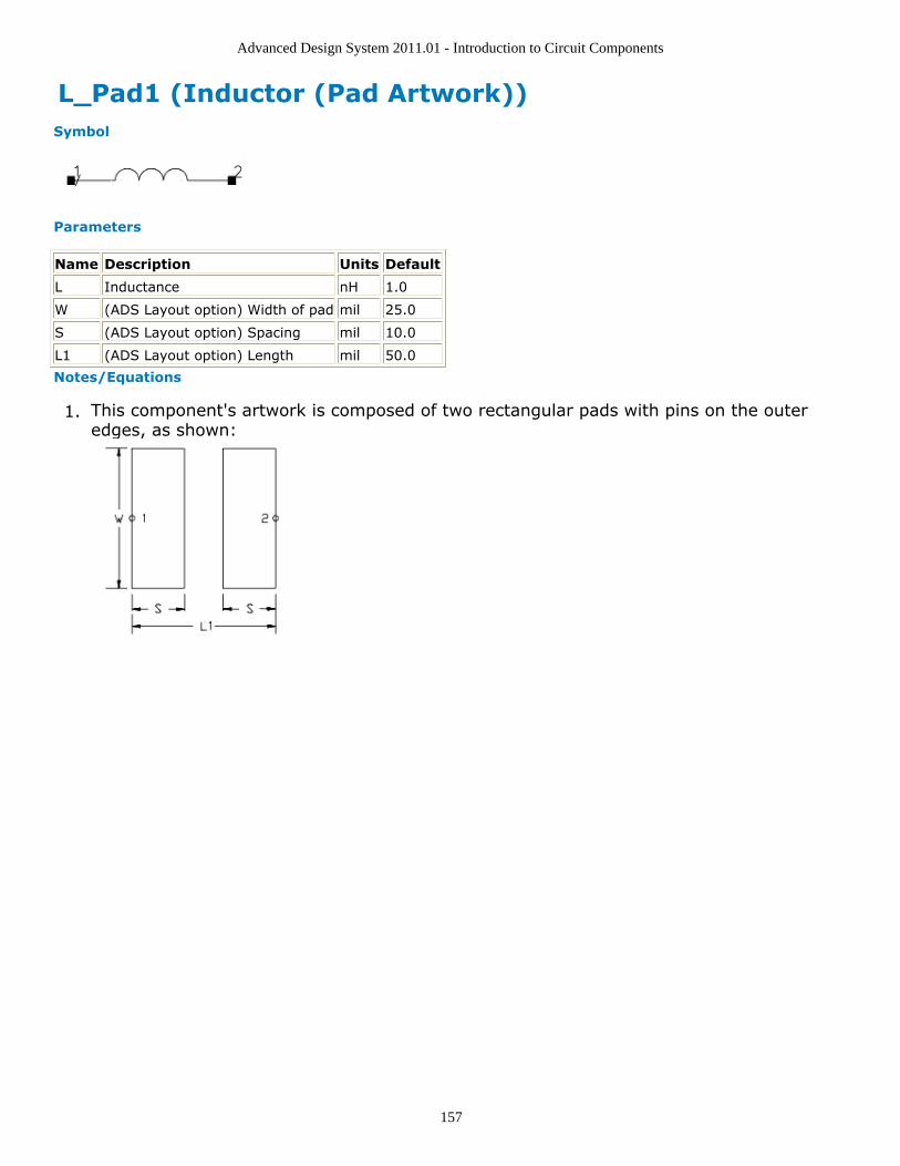
Advanced Design System 2011.01 - Introduction to Circuit Components
157
L_Pad1 (Inductor (Pad Artwork)) Symbol
Parameters
Name Description Units Default
L Inductance nH 1.0
W (ADS Layout option) Width of pad mil 25.0
S (ADS Layout option) Spacing mil 10.0
L1 (ADS Layout option) Length mil 50.0
Notes/Equations
This component's artwork is composed of two rectangular pads with pins on the outer1.edges, as shown:

Advanced Design System 2011.01 - Introduction to Circuit Components
158
LQ_Conn (Inductor with Q (Connector Artwork)) Symbol
Parameters
Name Description Units Default
L Inductance nH 1.0
Q Quality factor None 50.0
F Reference frequency for Q MHz 100.0
Mode Frequency dependence mode of Q; options (also refer to notes):
1=proportional to freq2=proportional to sqrt(freq)3=constant
None 1
Temp Temperature °C 25
Range of Usage
F ≥ 0
Notes/Equations
1.where:Mode Setting Q G
proportional to freq Q(f) = Q(F) f/F G(f) = G(F)
proportional to sqrt (freq) Q(f) = Q(F) G(f) = G(F)
constant Q(f) = Q(F) G(f) = G(F) f/F
If F is set to zero, then Q is assumed to be infinite. where f = simulation frequencyF = reference frequencyG = conductance of capacitorFor time-domain analysis, the frequency-domain analytical model is used.2.This component is a single connection in layout. For example, it can be used to3.represent parasitics.
Equivalent Circuit

Advanced Design System 2011.01 - Introduction to Circuit Components
159
LQ_Pad1 (Inductor with Q (Pad Artwork)) Symbol
Parameters
Name Description Units Default
L Inductance nH 1.0
Q Quality factor None 50.0
F Reference frequency for Q MHz 100.0
Mode Loss mode for this device; options (also refer to notes):1=proportional to freq2=proportional to sqrt(freq)3=constant
None 1
Temp Temperature °C 25
W (ADS Layout option) Width of pad mil 25.0
S (ADS Layout option) Spacings mil 10.0
L1 (ADS Layout option) Pin-to-pin distance mil 50.0
Range of Usage
F ≥ 0
Notes/Equations
1.where:Mode Setting Q G
proportional to freq Q(f) = Q(F) f/F G(f) = G(F)
proportional to sqrt (freq) Q(f) = Q(F) G(f) = G(F)
constant Q(f) = Q(F) G(f) = G(F) f/F
If F is set to zero, then Q is assumed to be infinite. where f = simulation frequencyF = reference frequencyG = conductance of capacitorFor time-domain analysis, the frequency-domain analytical model is used.2.This component's artwork is composed of two rectangular pads with pins on the outer3.edges, as shown:

Advanced Design System 2011.01 - Introduction to Circuit Components
160
Equivalent Circuit

Advanced Design System 2011.01 - Introduction to Circuit Components
161
LQ_Space (Inductor with Q (Space Artwork)) Symbol
Parameters
Name Description Units Default
L Inductance nH 1.0
Q Quality factor None 50.0
F Reference frequency for Q MHz 100.0
Mode Loss mode for this device; options (also refer to notes):1=proportional to freq2=proportional to sqrt(freq)3=constant
None 1
Temp Temperature °C 25
L1 (ADS Layout option) Pin-to-pin distance mil 50
Range of Usage
F ≥ 0
Notes/Equations
where: 1.Mode Setting Q G
proportional to freq Q(f) = Q(F) f/F G(f) = G(F)
proportional to sqrt (freq) Q(f) = Q(F) G(f) = G(F)
constant Q(f) = Q(F) G(f) = G(F) f/F
If F is set to zero, then Q is assumed to be infinite. where f = simulation frequencyF = reference frequencyG = conductance of capacitorFor time-domain analysis, the frequency-domain analytical model is used.2.This component is represented as a connected gap in layout---into which a custom3.artwork object can be inserted.
Equivalent Circuit
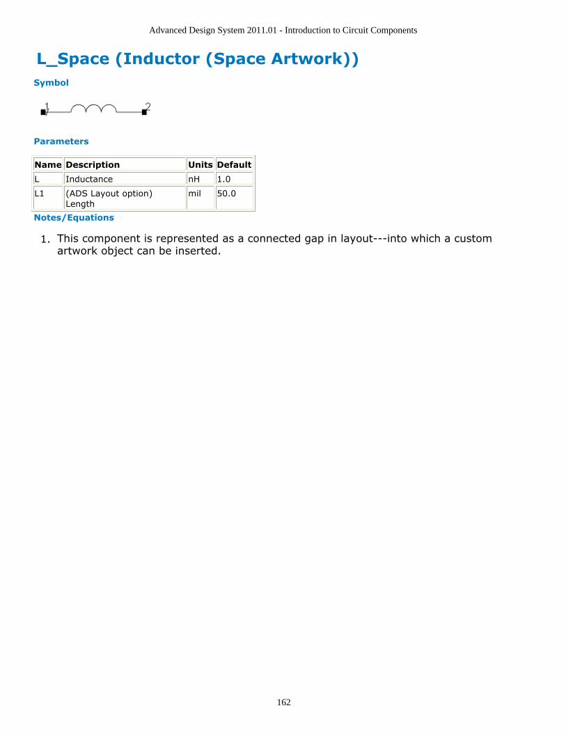
Advanced Design System 2011.01 - Introduction to Circuit Components
162
L_Space (Inductor (Space Artwork)) Symbol
Parameters
Name Description Units Default
L Inductance nH 1.0
L1 (ADS Layout option)Length
mil 50.0
Notes/Equations
This component is represented as a connected gap in layout---into which a custom1.artwork object can be inserted.
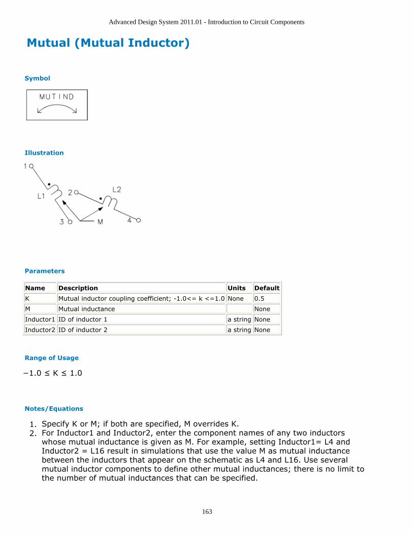
Advanced Design System 2011.01 - Introduction to Circuit Components
163
Mutual (Mutual Inductor)
Symbol
Illustration
Parameters
Name Description Units Default
K Mutual inductor coupling coefficient; -1.0<= k <=1.0 None 0.5
M Mutual inductance None
Inductor1 ID of inductor 1 a string None
Inductor2 ID of inductor 2 a string None
Range of Usage
−1.0 ≤ K ≤ 1.0
Notes/Equations
Specify K or M; if both are specified, M overrides K.1.For Inductor1 and Inductor2, enter the component names of any two inductors2.whose mutual inductance is given as M. For example, setting Inductor1= L4 andInductor2 = L16 result in simulations that use the value M as mutual inductancebetween the inductors that appear on the schematic as L4 and L16. Use severalmutual inductor components to define other mutual inductances; there is no limit tothe number of mutual inductances that can be specified.

Advanced Design System 2011.01 - Introduction to Circuit Components
164
Note To edit string parameters on a schematic, highlight the parameter and enter a value enclosedwith double quote symbols.
The ends of the inductors that are in-phase are identified by a small open circle on3.the schematic symbol for the inductors.Mutual inductor components can be placed anywhere on the schematic; they do not4.effect auto-layout.DC Operating Point Information lists the DC operating point parameters that can be5.sent to the dataset.
Name Description Units
M Mutual inductance H

Advanced Design System 2011.01 - Introduction to Circuit Components
165
PLC (Parallel Inductor-Capacitor)
Symbol
Parameters
Name Description Units Default
L Inductance nH 1.0
C Capacitance pF 1.0
Notes/Equations
Use for high Q circuits rather than individual components in parallel.1.This component has no default artwork associated with it.2.
Equivalent Circuit

Advanced Design System 2011.01 - Introduction to Circuit Components
166
PLCQ (Parallel Inductor-Capacitor with Q)
Symbol
Parameters
Name Description Units Default
L Capacitance nH 120.0
Ql Quality factor of inductor None 50.0
Fl Frequency at which Q is defined MHz 100.0
Mode Frequency dependence mode of inductor Q; options (also refer to notes): None 1
C Capacitance pF 21.0
Qc Quality factor of capacitor None 100.0
Fc Frequency at which capacitor Q is given MHz 100.0
ModC Frequency dependence mode of capacitor Q; options (also refer tonotes):
None 1
Rdc Resistance for modes 2 and 3 Ohm 0.0
Temp Temperature °C 25
Notes/Equations
Use for high Q circuits, rather than individual components in parallel.1.
(for inductors) (for capacitors) where 2.ModL Setting Ql ModC Setting Ql Qc
proportional to freq Ql(Fl) fs/Fl proportional to freq Qc(Fc) fs/Fc
proportional to sqrt (freq) Q(f) = Q(F) G(f) = G(F) proportional to sqrt (freq)
constant Ql(Fl) constant Qc(Fc)
where R = resistance of inductor G= conductance of capacitor fs = simulation frequency Fc, Fl = specified Qfrequencies
For time-domain analysis, the frequency-domain analytical model is used.3.This component has no default artwork associated with it.4.

Advanced Design System 2011.01 - Introduction to Circuit Components
167
Equivalent Circuit

Advanced Design System 2011.01 - Introduction to Circuit Components
168
PRC (Parallel Resistor-Capacitor)
Symbol
Parameters
Name Description Units Default
R Resistance Ohm 1.0
C Capacitance pF 1.0
Temp Temperature °C 25
Notes/Equations
This component has no default artwork associated with it.1.
Equivalent Circuit
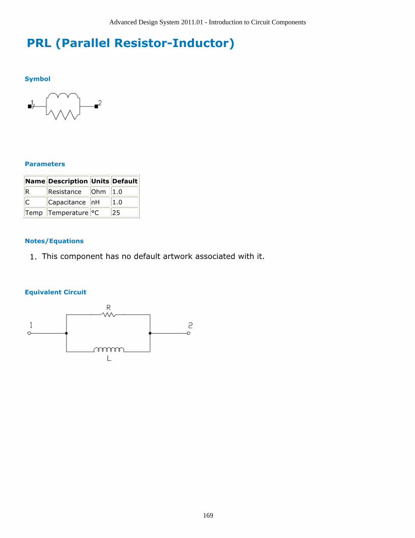
Advanced Design System 2011.01 - Introduction to Circuit Components
169
PRL (Parallel Resistor-Inductor)
Symbol
Parameters
Name Description Units Default
R Resistance Ohm 1.0
C Capacitance nH 1.0
Temp Temperature °C 25
Notes/Equations
This component has no default artwork associated with it.1.
Equivalent Circuit
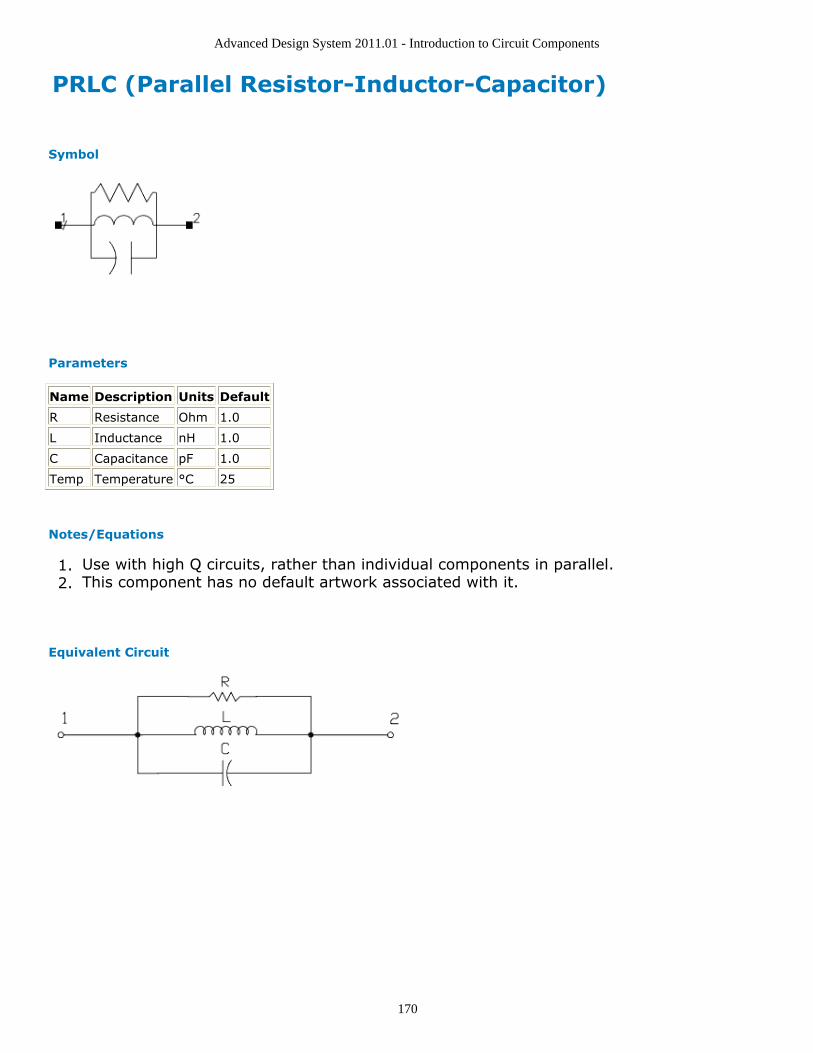
Advanced Design System 2011.01 - Introduction to Circuit Components
170
PRLC (Parallel Resistor-Inductor-Capacitor)
Symbol
Parameters
Name Description Units Default
R Resistance Ohm 1.0
L Inductance nH 1.0
C Capacitance pF 1.0
Temp Temperature °C 25
Notes/Equations
Use with high Q circuits, rather than individual components in parallel.1.This component has no default artwork associated with it.2.
Equivalent Circuit

Advanced Design System 2011.01 - Introduction to Circuit Components
171
R (Resistor)
Symbol
Parameters
Name Description Units Default
R Resistance Ohm 50
Temp Temperature °C 25
Trise Temperature rise above ambient °C None
Tnom Nominal temperature; see Note °C None
TC1 Temperature coefficient; per degree Celsius 1/°C None
TC2 Temperature coefficient; per degree Celsius squared 1/°C2 None
Noise Resistor thermal noise option: yes=enable;no=disable
None yes
wPmax Maximum power dissipation (warning) None
wImax Maximum current (warning) None
Model Name of a resistor model to use None None
Width Physical width for use with a model None
Length Physical length for use with a model None
_M Number of resistors in parallel None 1
C Capacitance F 0.0
Notes/Equations
The resistor value can be made a function of temperature by setting Tnom and TC11.or TC2 or both. Tnom specifies the nominal temperature at which R is given. Tnomdefaults to 25°C. If TempTnom, then the simulated resistance value is given by:R′ = R [1 + TC1 (Temp - Tnom) + TC2 (Temp - Tnom)2]If Temp is not explicitly specified, it defaults to the global temperature specified in2.the options item.The resistor generates thermal noise:3.<i2> = 4kT/RNoise generation can be disabled by setting Noise=no.wPmax and wImax are used by the overload alert feature. They set limits on the4.maximum instantaneous power dissipated by the resistor and maximum currentthrough the resistor. If these limits are specified, the simulator will issue a warningthe first time they are exceeded during a dc, harmonic balance or transientsimulation. Simulation results are not affected by this parameter.For a transient simulation, the resistance can vary with time. The resistance value5.

Advanced Design System 2011.01 - Introduction to Circuit Components
172
should be assigned an expression that is a function of the reserved variable time,which is the simulation time in seconds.If a model name is given, then values that are not specified on the resistor instance6.are taken from the model values. Typical values that can be defaulted are resistance,length and width, nominal temperature, temperature coefficients, and overload alertparameters.If a model is used, the resistance value to be simulated (before temperature scalingis applied) is calculated as:
_M is used to represent the number of resistors in parallel and defaults to 1. M7.cannot be zero. If a resistor model is used, an optional scaling parameter Scale canalso be defined on the model; it defaults to 1. The effective resistance that will besimulated is R Scale/M.DC Operating Point Information lists the DC operating point parameters that can be8.sent to the dataset.
Name Description Units
I Current A
Power DC powerdissipated
W
R Resistance Ohms
V Resistor voltage V
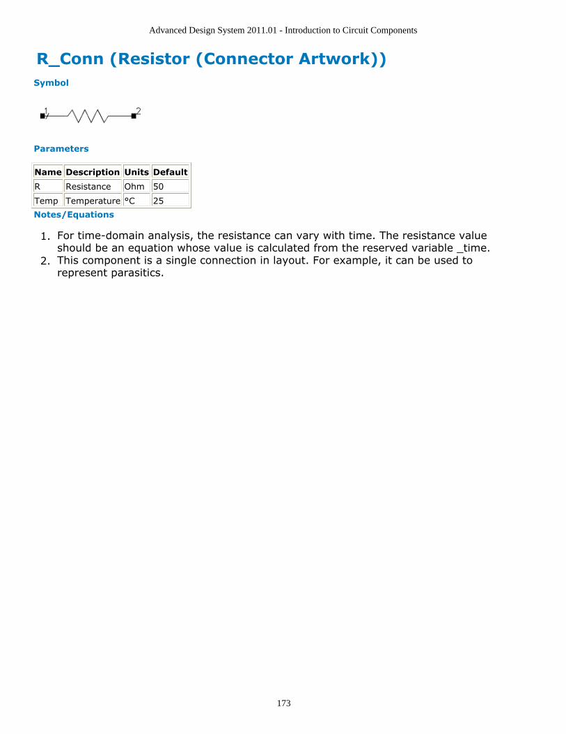
Advanced Design System 2011.01 - Introduction to Circuit Components
173
R_Conn (Resistor (Connector Artwork)) Symbol
Parameters
Name Description Units Default
R Resistance Ohm 50
Temp Temperature °C 25
Notes/Equations
For time-domain analysis, the resistance can vary with time. The resistance value1.should be an equation whose value is calculated from the reserved variable _time.This component is a single connection in layout. For example, it can be used to2.represent parasitics.

Advanced Design System 2011.01 - Introduction to Circuit Components
174
R_dxdy (Resistor (Delta X - Delta Y)) Symbol
Parameters
Name Description Units Default
R Resistance Ohm 0
dx Delta X mil 50.0
dy Delta Y mil 50.0
Temp Temperature °C 25
Notes/Equations
This component shifts the next artwork in X/Y direction during layout in design1.synchronization from schematic to layout.

Advanced Design System 2011.01 - Introduction to Circuit Components
175
reluctance
Parameters
Name Description Units Default
reluctance Reluctance matrix data. In general, K will be sparse and only non-zerovalues in the matrix need be given. Each matrix entry is represented by atriplet (r,c,val). See Note 4, 5, 6, 7.
H-1 no valueunless set byuser
file The data files should contain three columns of data. Each row shouldcontain an (r,c,value) triplet separated by white space. See Note 4, 5, 6, 7.
no valueunless set byuser
Netlist Format
Inline form:
reluctance: <InstanceName> n1p n1n [n2p n2n ....... nNp nNn]
reluctance=list(r1, c1, val1 [, r2, c2, val2, ......] )
External file reference form:
reluctance: <InstanceName> n1p n1n [n2p n2n ....... nNp nNn]
file="<Filename>"
For more information about the ADS circuit simulator netlist format, refer to ADSSimulator Input Syntax (cktsim).
Notes/Equations
The reluctance element is used to model the parasitic inductive effect of1.interconnects, which is a must for the accurate simulation of high-speed digital,analog and RF designs.The parasitic inductive effect is traditionally modeled by the inductance matrix. The2.reluctance matrix is the inverse of the inductance matrix. This new approach of usingthe reluctance matrix has the following advantages over the traditional one:
The reluctance matrix is easier to extract in a stable manner.The reluctance matrix is much sparser than the inductance matrix and allows formore efficient simulation.
The reluctance element is a linear N-Port network, the relationship between the port3.voltages and currents is governed by the following matrix equation:

Advanced Design System 2011.01 - Introduction to Circuit Components
176
The value r and c are integers referring to a pair of inductors from the list of terminal4.nodes. If there are 2*N terminal nodes, there will be N inductors, and the r and cvalues must be in the range [1,N]. The val value is a reluctance value for the ( r , c )matrix location.Only terms along and above the diagonal are specified for the reluctance matrix. The5.simulator fills in the lower triangle to ensure symmetry. If you specify lower diagonalterms, the simulator converts that entry to the appropriate upper diagonal term. Ifmultiple entries are supplied for the same ( r , c ) location, only the first one is used,and a warning will be issued indicating some entries are ignored.All diagonal entries of the reluctance matrix must be assigned a positive value.6.Otherwise, a warning will be issued to point out the non-positive diagonal entries.The simulation will still proceed with the values specified by the user.The reluctance matrix should be positive definite. The simulator checks that off-7.diagonal terms should be smaller in magnitude than the diagonal term in the samerow/column.

Advanced Design System 2011.01 - Introduction to Circuit Components
177
R_Model (Resistor Model)
Symbol
Parameters
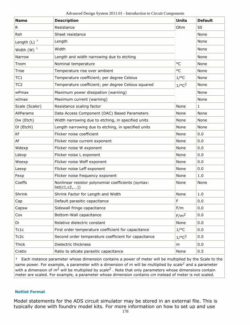
Advanced Design System 2011.01 - Introduction to Circuit Components
178
Name Description Units Default
R Resistance Ohm 50
Rsh Sheet resistance None
Length (L) † Length None
Width (W) † Width None
Narrow Length and width narrowing due to etching None
Tnom Nominal temperature °C None
Trise Temperature rise over ambient °C None
TC1 Temperature coefficient; per degree Celsius 1/°C None
TC2 Temperature coefficient; per degree Celsius squared 1/°C2 None
wPmax Maximum power dissipation (warning) None
wImax Maximum current (warning) None
Scale (Scaler) Resistance scaling factor None 1
AllParams Data Access Component (DAC) Based Parameters None None
Dw (Etch) Width narrowing due to etching, in specified units None None
Dl (Etchl) Length narrowing due to etching, in specified units None None
Kf Flicker noise coefficient None 0.0
Af Flicker noise current exponent None 0.0
Wdexp Flicker noise W exponent None 0.0
Ldexp Flicker noise L exponent None 0.0
Weexp Flicker noise Weff exponent None 0.0
Leexp Flicker noise Leff exponent None 0.0
Fexp Flicker noise frequency exponent None 1.0
Coeffs Nonlinear resistor polynomial coefficients (syntax:list(c1,c2,...))
None None
Shrink Shrink Factor for Length and Width None 1.0
Cap Default parasitic capacitance F 0.0
Capsw Sidewall fringe capacitance F/m 0.0
Cox Bottom-Wall capacitance F/m2 0.0
Di Relative dielectric constant None 0.0
Tc1c First order temperature coefficient for capacitance 1/°C 0.0
Tc2c Second order temperature coefficient for capacitance 1/°C2 0.0
Thick Dielectric thickness m 0.0
Cratio Ratio to allcate parasitic capacitance None 0.5
† Each instance parameter whose dimension contains a power of meter will be multiplied by the Scale to thesame power. For example, a parameter with a dimension of m will be multiplied by scale1 and a parameterwith a dimension of m2 will be multiplied by scale2 . Note that only parameters whose dimensions containmeter are scaled. For example, a parameter whose dimension contains cm instead of meter is not scaled.
Netlist Format
Model statements for the ADS circuit simulator may be stored in an external file. This istypically done with foundry model kits. For more information on how to set up and use

Advanced Design System 2011.01 - Introduction to Circuit Components
179
foundry model kits, refer to Design Kit Development (dkarch).
model modelname R_Model [parm=value]*
The model statement starts with the required keyword model . It is followed by themodelname that will be used by resistor components to refer to the model. The thirdparameter indicates the type of model; for this model it is _R_Model_ . The rest of themodel contains pairs of model parameters and values, separated by an equal sign. Thename of the model parameter must appear exactly as shown in the parameters table-these names are case sensitive. Some model parameters have aliases, which are listed inparentheses after the main parameter name; these are parameter names that can beused instead of the primary parameter name. Model parameters may appear in any orderin the model statement. Model parameters that are not specified take the default valueindicated in the parameters table. For more information about the ADS circuit simulatornetlist format, refer to ADS Simulator Input Syntax (cktsim).Example:
model polyRes R_Model \
Rsh=100 Etch=2.5e-8 TC1=50e-6 \
Coeffs=list(1,2)
Notes/Equations
R_Model supplies model parameters for use with a resistor R. This allows physically-1.based resistors to be modeled based on length and width.When the physical parameters Rsh, Width and Length are specified, wImax is the2.current limit in amperes/meter:
If the physical parameters Rsh, Width and Length are not specified, wImax is thecurrent limit in amperes.Use AllParams with a DataAccessComponent to specify file-based parameters (refer3.to DataAccessComponent). Note that model parameters that are explicitly specifiedtake precedence over those specified via AllParams.Flicker noise is modeled using the equation:4.
The resistor value can be made a nonlinear function of the applied voltage V by5.specifying the polynomial coefficients list (Coeffs = list(c1, c2, c3, ...) ). Theresistance value R ( V ) is then given by:Leexp
where R is the resistance of the instance, and ck is the k -th entry in the Coeffs list.The branch current as a function of the applied voltage is:

Advanced Design System 2011.01 - Introduction to Circuit Components
180
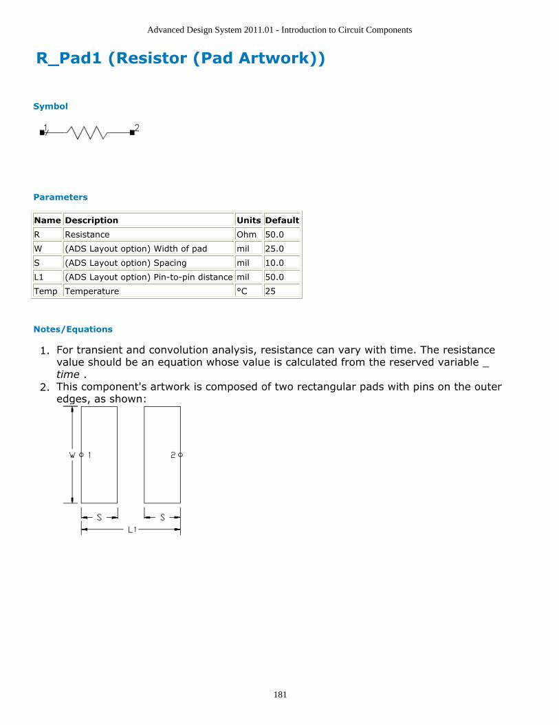
Advanced Design System 2011.01 - Introduction to Circuit Components
181
R_Pad1 (Resistor (Pad Artwork))
Symbol
Parameters
Name Description Units Default
R Resistance Ohm 50.0
W (ADS Layout option) Width of pad mil 25.0
S (ADS Layout option) Spacing mil 10.0
L1 (ADS Layout option) Pin-to-pin distance mil 50.0
Temp Temperature °C 25
Notes/Equations
For transient and convolution analysis, resistance can vary with time. The resistance1.value should be an equation whose value is calculated from the reserved variable _time .This component's artwork is composed of two rectangular pads with pins on the outer2.edges, as shown:

Advanced Design System 2011.01 - Introduction to Circuit Components
182
R_Space (Resistor (Space Artwork)) Symbol
Parameters
Name Description Units Default
R Resistance Ohm 50
L1 (ADS Layout option) Pin-to-pindistance
mil 50.0
Temp Temperature °C 25
Notes/Equations
For time-domain analysis, the resistance can vary with time. The resistance value1.should be an equation whose value is calculated from the reserved variable _time.This component is represented as a connected gap in layout---into which a custom2.artwork object can be inserted.

Advanced Design System 2011.01 - Introduction to Circuit Components
183
Short (Short)
Symbol
Parameters
Name Description Units Default
Mode Integer values denote functionality: None 0
C DC block capacitance None
L DC feed inductance None
Gain Current gain None None
SaveCurrent Save branch current: yes or no None no
wImax Maximum current (warning) None
Notes/Equations
This component behaves like a current probe. It can be used to measure the current1.anywhere in the circuit.The variable name for the current is label.i , where label is the label of this2.component.DC Operating Point Information lists the DC operating point parameters that can be3.sent to the dataset.
Name Description Units
I Current A

Advanced Design System 2011.01 - Introduction to Circuit Components
184
SLC (Series Inductor-Capacitor)
Symbol
Parameters
Name Description Units Default
L Inductance nH 1.0
C Capacitance pF 1.0
Notes/Equations
Use when modeling high Q circuits as opposed to two individual components1.This component has no default artwork associated with it.2.
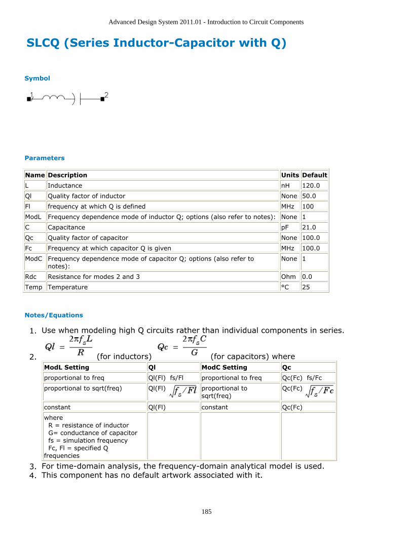
Advanced Design System 2011.01 - Introduction to Circuit Components
185
SLCQ (Series Inductor-Capacitor with Q)
Symbol
Parameters
Name Description Units Default
L Inductance nH 120.0
Ql Quality factor of inductor None 50.0
Fl frequency at which Q is defined MHz 100
ModL Frequency dependence mode of inductor Q; options (also refer to notes): None 1
C Capacitance pF 21.0
Qc Quality factor of capacitor None 100.0
Fc Frequency at which capacitor Q is given MHz 100.0
ModC Frequency dependence mode of capacitor Q; options (also refer tonotes):
None 1
Rdc Resistance for modes 2 and 3 Ohm 0.0
Temp Temperature °C 25
Notes/Equations
Use when modeling high Q circuits rather than individual components in series.1.
(for inductors) (for capacitors) where2.ModL Setting Ql ModC Setting Qc
proportional to freq Ql(Fl) fs/Fl proportional to freq Qc(Fc) fs/Fc
proportional to sqrt(freq) Ql(Fl) proportional tosqrt(freq)
Qc(Fc)
constant Ql(Fl) constant Qc(Fc)
where R = resistance of inductor G= conductance of capacitor fs = simulation frequency Fc, Fl = specified Qfrequencies
For time-domain analysis, the frequency-domain analytical model is used.3.This component has no default artwork associated with it.4.

Advanced Design System 2011.01 - Introduction to Circuit Components
186
Equivalent Circuit

Advanced Design System 2011.01 - Introduction to Circuit Components
187
SMT_Pad (SMT Bond Pad) Symbol
Illustration
Parameters
Name Description Units Default
W Width of pad mil 10.0
L Length of pad mil 25.0
PadLayer Layer of pad select from layeroptions
bond
SMO Solder mask overlap mil 5.0
SM_Layer Solder mask layer select from layeroptions
solder_mask
PO Pad offset from connection pin mil 0
Range of Usage
W ≥ 0L ≥ 0
Notes/Equations
This component is required for layout of SMT library parts.1.For any library item to which this component is attached, the PO parameter specifies2.the offset of the bond pad center from the position of pin connections designated forthat item's package artwork. An offset of 0 centers the pad around the location of thepins. A positive value shifts the pad away from the package body; a negative valueshifts the pad toward the package body.A positive value for SMO increases the area of the solder mask; a negative value3.decreases it.
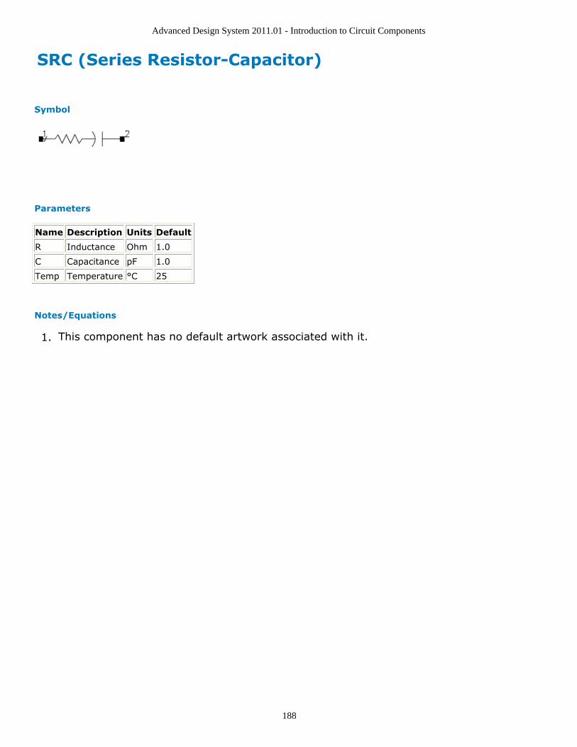
Advanced Design System 2011.01 - Introduction to Circuit Components
188
SRC (Series Resistor-Capacitor)
Symbol
Parameters
Name Description Units Default
R Inductance Ohm 1.0
C Capacitance pF 1.0
Temp Temperature °C 25
Notes/Equations
This component has no default artwork associated with it.1.
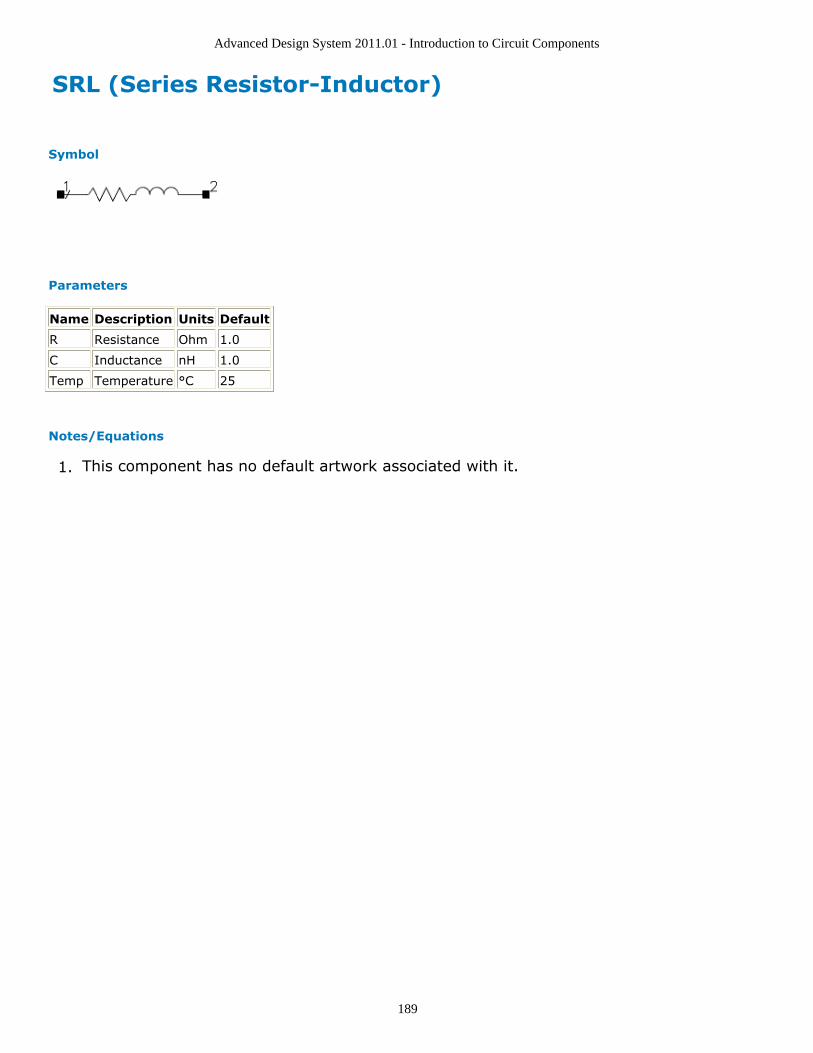
Advanced Design System 2011.01 - Introduction to Circuit Components
189
SRL (Series Resistor-Inductor)
Symbol
Parameters
Name Description Units Default
R Resistance Ohm 1.0
C Inductance nH 1.0
Temp Temperature °C 25
Notes/Equations
This component has no default artwork associated with it.1.
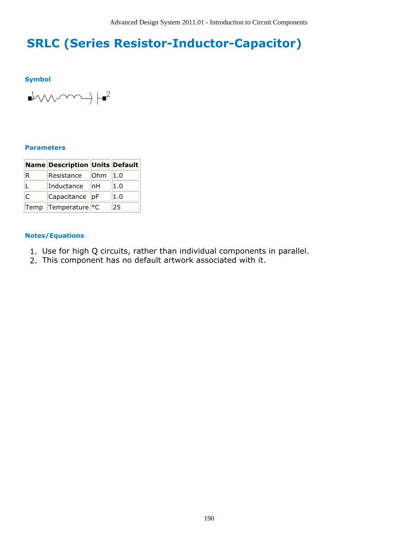
Advanced Design System 2011.01 - Introduction to Circuit Components
190
SRLC (Series Resistor-Inductor-Capacitor)
Symbol
Parameters
Name Description Units Default
R Resistance Ohm 1.0
L Inductance nH 1.0
C Capacitance pF 1.0
Temp Temperature °C 25
Notes/Equations
Use for high Q circuits, rather than individual components in parallel.1.This component has no default artwork associated with it.2.

Advanced Design System 2011.01 - Introduction to Circuit Components
191
TF3 (3-Port Transformer)
Symbol
Parameters
Name Description Units Default
T1 Turn 1 None 1.00
T2 Turn 2 None 1.00
Notes/Equations
The turns ratio T is the ratio of turns in the secondary to turns in the primary:1.
A turns ratio less than 1 describes a transformer in which there are more turns in the2.secondary than in the primary. Parasitic inductances of the primary and secondaryare not modeled; to do this, use the component for mutual inductance (M).The ends that are in phase are identified by a small open circle on the schematic3.symbol.DC voltages are also converted.4.

Advanced Design System 2011.01 - Introduction to Circuit Components
192
TF (Transformer)
Symbol
Parameters
Name Description Units Default
T Turns ratio T1/T2 None 1.00
Notes/Equations
The turns ratio T is the ratio of turns in the primary to turns in the secondary (T:1).1.A turns ratio less than 1 describes a transformer in which there are more turns in thesecondary than in the primary.The TF component is a Hybrid component with the parameters H12=T and H21=-T.2.For more information on Hybrid components, refer to "Hybrid (2-Port User-DefinedLinear Hybrid)".Parasitic inductances of the primary and secondary are not modeled. To do this, use3.the mutual inductance component "Mutual" located on the Lumped-Componentspalette. The ends that are in phase are identified by a small open circle on theschematic symbol.Because this is an ideal transformer, the impedance transformation is the same at DC4.as it is at nonzero frequencies.This component passes DC.5.

Advanced Design System 2011.01 - Introduction to Circuit Components
193
Miscellaneous Circuit ComponentsCAPP2 (Chip Capacitor) (ccsim)CIND (Ideal Torroidal Inductor) (ccsim)RIND (Rectangular Inductor) (ccsim)XFERP (Physical Transformer) (ccsim)XFERRUTH (Ruthroff Transformer) (ccsim)XFERTAP (Tapped Secondary Ideal Transformer) (ccsim)

Advanced Design System 2011.01 - Introduction to Circuit Components
194
CAPP2 (Chip Capacitor)
Symbol
Parameters
Name Description Units Default
C Capacitance pF 1.0
TanD Dielectric loss tangent None 0.001
Q Quality factor None 50.0
FreqQ Reference frequency for Q MHz 300.0
FreqRes Resonance frequency MHz 500.0
Exp Exponent for frequency dependence of Q None 2.0
Temp Temperature °C 25
Range of Usage
C, Q, FreqQ, FreqRes ≥ 0
Notes/Equations
The series resistance Rs is determined by the Q and the parallel resistance Rp is1.
determined by TanD.The frequency-dependence of Q is given byQ (f) = Q (FreqQ) × (FreqQ/f)EXP
where f is the simulation frequency and Q(FreqQ) is the specified value of Q atFreqQ.If Q or FreqQ are set to 0, Q is assumed to be infinite.2.For time-domain analysis, the frequency-domain analytical model is used.3.This component has no default artwork associated with it.4.
References
C. Bowick, RF Circuit Design , Howard Sams & Co., 1987.1.The RF Capacitor Handbook , American Technical Ceramics Corp., September 1983.2.

Advanced Design System 2011.01 - Introduction to Circuit Components
195
Equivalent Circuit

Advanced Design System 2011.01 - Introduction to Circuit Components
196
CIND (Ideal Torroidal Inductor)
Symbol
Illustration
Parameters
Name Description Units Default
N Number of units None 10.0
AL Inductance index nH 0.15
Range of Usage
N, AL > 0
Notes/Equations
The inductance is given by1.L = N2 × ALThis component has no default artwork associated with it.2.

Advanced Design System 2011.01 - Introduction to Circuit Components
197
RIND (Rectangular Inductor)
Symbol
Illustration
Parameters
Name Description Units Default
N Number of turns (need not be an integer) None 3.0
L1 Length of second outermost segment mil 30.0
L2 Length of outermost segment mil 20.0
W Conductor width mil 1.0
S Conductor spacing mil 1.0
T Conductor thickness mil 0.2
Rho Conductor resistivity (relative to copper) None 1.0
FR Resonant frequency MHz 10.0
Temp Physical temperature °C 25
Range of Usage
N must be such that all segments fit given L1, L2, W, and S.
Notes/Equations

Advanced Design System 2011.01 - Introduction to Circuit Components
198
Notes/Equations
For time-domain analysis, an impulse response obtained from the frequency-domain1.analytical model is used.This component has no default artwork associated with it.2.
References
H. M. Greenhouse, "Design of Planar Rectangular Microelectronic Inductors," IEEE1.Transactions as Parts, Hybrids, and Packaging, Vol. PHP-10, No. 2, June 1974, pp.101-109.
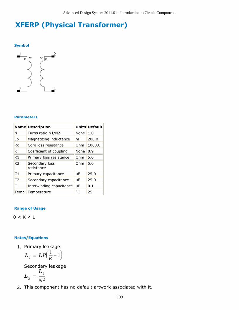
Advanced Design System 2011.01 - Introduction to Circuit Components
199
XFERP (Physical Transformer)
Symbol
Parameters
Name Description Units Default
N Turns ratio N1/N2 None 1.0
Lp Magnetizing inductance nH 200.0
Rc Core loss resistance Ohm 1000.0
K Coefficient of coupling None 0.9
R1 Primary loss resistance Ohm 5.0
R2 Secondary lossresistance
Ohm 5.0
C1 Primary capacitance uF 25.0
C2 Secondary capacitance uF 25.0
C Interwinding capacitance uF 0.1
Temp Temperature °C 25
Range of Usage
0 < K < 1
Notes/Equations
Primary leakage:1.
Secondary leakage:
This component has no default artwork associated with it.2.

Advanced Design System 2011.01 - Introduction to Circuit Components
200
Equivalent Circuit

Advanced Design System 2011.01 - Introduction to Circuit Components
201
XFERRUTH (Ruthroff Transformer)
Symbol
Parameters
Name Description Units Default
N Number of turns None 1.0
AL Inductance index nH 1.0
Z Characteristic impedance of transmission line Ohm 50.0
E Electrical length of transmission line deg 90
F Reference frequency for electrical length MHz 1.0
Range of Usage
N > 0AL > 0
Notes/Equations
Inductance: L = N2 × AL1.This component has no default artwork associated with it.2.
References
H. L. Krauss and C. W. Allen. "Designing torroidal transformers to optimize wideband1.performance," Electronics, pp. 113-116, August 16, 1973.O. Pitzalis, Jr. and T. P. Couse. "Practical Design Information for Broadband2.Transmission Line Transformers," Proceedings of the IEEE , Vol. 56, No. 4(Proceedings Letters), April 1968, pp. 738-739.C. L. Ruthroff. "Some Broadband Transformers," Proceedings of the IRE, Vol. 47, No.3.8, August 1959, pp. 1337-1342 (Fig. 3, page 1338, in particular).
Equivalent Circuit

Advanced Design System 2011.01 - Introduction to Circuit Components
202
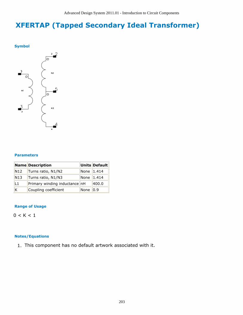
Advanced Design System 2011.01 - Introduction to Circuit Components
203
XFERTAP (Tapped Secondary Ideal Transformer)
Symbol
Parameters
Name Description Units Default
N12 Turns ratio, N1/N2 None 1.414
N13 Turns ratio, N1/N3 None 1.414
L1 Primary winding inductance nH 400.0
K Coupling coefficient None 0.9
Range of Usage
0 < K < 1
Notes/Equations
This component has no default artwork associated with it.1.

Advanced Design System 2011.01 - Introduction to Circuit Components
204
Probe ComponentsCounter (Counter Component) (ccsim)EyeDiff Probe (Differential Eye Measurement Probe) (ccsim)Eye Probe (Eye Measurement Probe) (ccsim)I Probe (Current Probe) (ccsim)OscPort2 (Differential Oscillator Port) (ccsim)OscPort (Grounded Oscillator Port) (ccsim)OscTest (Grounded Oscillator Test) (ccsim)P Probe2 (Differential Power Probe) (ccsim)P Probe (Grounded Power Probe) (ccsim)SP Probe (S-Parameter Probe) (ccsim)SProbe2 (SProbe2 Component) (ccsim)SProbePair2 (SProbePair2 Component) (ccsim)TimeDelta (Time Delta Component) (ccsim)TimeFrq (Time Frequency Component) (ccsim)TimePeriod (Time Period Component) (ccsim)TimeStamp (Time Stamp Component) (ccsim)WaveformStats (WaveformStats Component) (ccsim)

Advanced Design System 2011.01 - Introduction to Circuit Components
205
Counter (Counter Component) Symbol
Parameters
Name Description Units Default
Direction Direction one None 1
Thresh Threshold one V 0
Notes/Equations
This time counter model generates an output voltage equal to the number of times1.that the user-specified trigger has occurred. The trigger point is defined by setting athreshold voltage and a slope. The slope can be specified as either rising or falling bysetting the direction parameter to a 1 or -1. A direction parameter value of 0 is usedif a trigger for either slope is desired.Only the baseband component of the input voltages is used to generate the trigger,2.so the model may be used in either envelope or transient time domain analysismodes. Linear interpolation is used to estimate the actual trigger crossing time to afiner resolution than the simulation time step.The input impedance is infinite. The output impedance is 1 ohm. The open circuit3.output voltage is equal to n, the number of triggers that have occurred up thepresent simulation time. This count does not change until a trigger event occurs, andis held constant until another event occurs.

Advanced Design System 2011.01 - Introduction to Circuit Components
206
EyeDiff_Probe (Differential Eye Measurement Probe) Symbol
Parameters
Name Description Units Default
Data Rate Signal data rate Gbps 1
Number of time points per UI Number of time points for eye histogram binning None 1000
Amplitude resolution Voltage resolution for eye histogram binning V 0.001
Lower boundary (%) Lower boundary for eye level computation None 40
Upper boundary (%) Upper boundary for eye level computation None 60
Lower threshold (%) Lower amplitude threshold for rise/fall time computation None 20
Upper threshold (%) Upper amplitude threshold for rise/fall time computation None 80
Disable transient analysis output Disables storage of transient waveforms to save diskspace
None yes
Notes/Equations
Provides a differential input for designs requiring use of the Eye_Probe component.1.For details about parameters and measurements, see Eye Probe (ccsim).The component is located on the Simulation-Transient palette.2.

Advanced Design System 2011.01 - Introduction to Circuit Components
207
Eye_Probe (Eye Measurement Probe) Symbol
Parameters
Name Description Units Default
Data Rate Signal data rate Gbps 1
BER width and height The bit error rate of a probability contour for WidthAtBERand HeightAtBER measurements
None 1e-12
BER contour List of bit error rates for computing probability contours None list(1e-12, 1e-11,1e-10)
Extrapolate in bit-by-bit mode
Enables BER extrapolation in bit-by-bit mode None no
Use eye mask Enables the eye mask specification and outputs the eyemask to dataset
None no
Disable transientanalysis output
Disables storage of transient waveforms to save diskspace
None yes
Number of time points Number of time points per 2 UI for eye histogram binning None 400
Amplitude resolution Voltage resolution for eye histogram binning V 0.001
Lower boundary (%) Lower boundary for eye level computation None 40
Upper boundary (%) Upper boundary for eye level computation None 60
Lower threshold (%) Lower amplitude threshold for rise/fall time computation None 20
Upper threshold (%) Upper amplitude threshold for rise/fall time computation None 80
Position from crossinglevel
Offset from eye crossing level for timing bathtubmeasurement
V 0.0
Position from crossingtime
Offset from eye crossing time for amplitude bathtubmeasurement
None(UI)
0.5
Notes/Equations
Description1.The Eye_Probe component displays eye diagrams and extracts statistical eye diagrammetrics such as probability bathtubs, BER contours, eye width, eye height, RMS jitterand rise/fall time. For many of the measurements, it uses the same algorithms as theEye Diagram FrontPanel (data) utility. Unlike the Eye Diagram FrontPanel, Eye_Probedoes not require stored circuit waveforms and does not rely on waveform post-processing in the data display. As a result, Eye_Probe measurements are significantlyfaster, require little disk space, and consume far less computer memory.
Eye_Probe components work with the Transient and Convolution (cktsimtrans) andChannel (cktsimchan) simulation controllers. They produce no output in any othersimulation analysis. In all cases, Eye_Probe components are open-circuited, whichmeans they do not have any electrical effect on the circuit.Eye_Probe component can only be attached to the Rx component in a Channel2.Simulation.

Advanced Design System 2011.01 - Introduction to Circuit Components
208
Location3.The Eye_Probe is located on the Simulation-Transient and Simulation-ChannelSimcomponent palettes, and uses the following icon:
Example Circuit4.After placing the Eye_Probe on the schematic, connect the probe to a circuit node asshown in the following figure. Two Eye_Probe components are shown in this example,but any number of probes may be placed in a circuit:
Parameters Setup Dialog5.To set Eye_Probe parameters, double-click on the symbol to open the componentsetup dialog box. There are two tabs:
Parameters: Sets Eye_Probe parameters common to all measurements.Measurements: Sets specific measurements for output to the data display.
By default, the Parameters tab shows a subset of commonly used parameters.To access all of the available parameters, click More to expand the parameterstab.
Setting Up the Parameters TabThe following table describes how parameter settings interact:

Advanced Design System 2011.01 - Introduction to Circuit Components
209
Parameter Description
Data rate This parameter should be set to the data rate of the incoming datastream. In transient simulation, Data rate is a required parameter. Inchannel simulation, this parameter is automatically synchronized to theBit rate parameter of the TX source.
BER width and height,BER contour
These parameters control the output of Contour, WidthAtBER andHeightAtBER measurements, as discussed below.
Use Eye Mask This parameter let you specify an eye mask and view it in the dataset, asdescribed in detail in section Eye Masks below.
Number of time pointsper UI,Amplitude resolution
These parameters set the horizontal and vertical resolution of the eyehistogram. Using finer resolution increases measurement accuracy at theexpense of larger disk storage and run-time memory requirements.
Lower boundary (%),Upper boundary (%)
Boundary parameters define the eye diagram boundary for thecomputation of quantities such as amplitude, height, and SNR. Lower andupper limits are defined as a percentage of a UI.
Lower threshold (%),Upper threshold (%)
Threshold parameters define the amplitude swing for rise and fall timecomputation.
Disable transientanalysis output
Use this parameter to prevent the output of transient waveforms to thedata display. By default, simulation controllers save all waveforms in ahierarchical design up to a specified level of hierarchy (see SelectivelySaving and Controlling Simulation Data (cktsim)). Waveform storagerequires a large amount of disk space in long transient simulations. Thisoption saves disk space by preventing default waveform storage fromtransient simulations. If the waveform at the node to which the probe isconnected is required, Eye_Probes provide an optional waveformmeasurement, to be discussed later.
Setting Up the Measurements TabThe Measurements tab offers a selection of measurements to be processed andsent to the data display. To move a measurement into the list of Selectedmeasurements, click a measurement name in the Available list, then click Add.The default selection includes Density, Height, Level1, Level0, and Width. Theavailable measurements are described in the following section.
Eye Histogram Measurement Equations6.Eye measurements are computed from the statistical properties of the 3-dimensionaleye histogram. The eye histogram is computed by counting the number of signalcrossings in the time-voltage plane. Histogram resolution is defined by the resolutionparameters on the Eye_Probe's setup dialog box on the Parameters tab.
Eye measurements can be loosely characterized as shown in the following table:Characterization Measurements
Vertical measurements Amplitude, Height, HeightDB, Level1, Level0, LevelMean, SNR
Horizontal measurements FallTime, JitterPP, JitterRMS, RiseTime, Width
BER measurements Contour, Bathtub, WidthAtBER, HeightAtBER
Miscellaneous measurements Density, Waveform, CheckMaskViolation
Vertical measurements are computed from the properties of the eye histogram inthe region defined by the Eye Level Boundaries parameters, as shown in followingfigure:

Advanced Design System 2011.01 - Introduction to Circuit Components
210
VerticalMeasurement
Description
Amplitude Computed as the difference between Level1 and Level0.
Height The distance between the 3-sigma points of the logic-1 and logic-0 histograms,measured across the eye level boundary.Height is calculated according to the formula:Height=(Level1-3*sigmalevel1) - (Level0+3*sigmalevel0)
HeightDB Calculated as 10log10(Height).
Level1 The mean of the eye vertical histogram in the upper half of the eye levelboundary.
Level0 The mean of the eye vertical histogram in the lower half of the eye levelboundary.
LevelMean Defined as the average of Level1 and Level0.
SNR SNR (signal-to-noise ratio) is calculated as SNR=Amplitude/(sigmalevel1 + sigma
level0).
Horizontal measurements are computed from the statistics of the crossinghistogram at certain amplitude thresholds as shown in the following figure:

Advanced Design System 2011.01 - Introduction to Circuit Components
211
HorizontalMeasurement
Description
JitterPP The peak-to-peak value, or width, of the crossing time histogram.
JitterRMS The standard deviation of the crossing time histogram.
RiseTime andFallTime
These measurements calculate the time between the mean crossings of the upperand lower amplitude thresholds. The upper and lower thresholds default to 80% and20%, respectively, and are controlled by the Amplitude Threshold parameters locatedon the Eye_Probe's Parameters tab. The thresholds are a percentage of the eyeAmplitude, defined above as Amplitude = Level1 - Level0.
Width Width is calculated according to the formula: Width=(t2 - 3*sigmat2) - (t1 + 3*sigma
t1).
t2 and t1 are the mean values of the crossing time histograms.
BER measurements are described in the following table:
BERMeasurement
Description
Contour This measurement computes contours of constant error probability and outputs themto dataset as BERContour. Any number of contours may be specified using the eyeprobe BER contour parameter. The contours are computed over 1 UI. If a contourdoesn't exist because its BER is below the system's minimum BER, a warning isprinted in the status window and the contour is not output to the dataset.
Bathtub This measurement computes the timing and amplitude bathtubs and outputs them todataset as TimingBathtub and VoltageBathtub, respectively. The voltage reference forthe timing bathtub is automatically set at the eye crossing level. Similarly, the timingreference for the voltage bathtub is automatically set at 0.5 UI offset from the eyecrossing. The timing and amplitude references may be changed using the eye probeparameters Position from crossing level and Position from crossing time.
WidthAtBER andHeightAtBER
Computes the maximum width and height of a contour at a BER specified using theBER width and height parameter
Miscellaneous measurements are described in the following table:
MiscellaneousMeasurement
Description
Density A temperature view of the 3-dimensional eye histogram. The eye isautomatically centered and displayed over 2UI on the horizontal axis. Colorindicates the number of crossings of a segment in the time-voltage plane. Blueareas are cold, whereas red indicates comparatively more crossings.
Waveform Stores the waveform at the node to which the probe is connected. By default,Eye_Probe components suppress standard waveform output from the transientsimulation controller. This option gives access to the waveform at the probenode, while suppressing default transient output and therefore preserving diskspace.
CheckMaskViolation Compares the Density measurement to the specified eye mask and reportsresults as MaskViolated in the data display. If the mask is violated by the eyedensity plot, MaskViolated is set to 1.
Output7.The Eye_Probe stores the chosen measurements in a dataset for viewing in the datadisplay as shown in the following figure:

Advanced Design System 2011.01 - Introduction to Circuit Components
212
In addition to the chosen measurements, a Summary table is available to display allof the measurements in a convenient format, as shown in the following figure. Incase of multiple probes, the measurement is prefixed by the Eye_Probe's instancename.
Measurement availability in transient and channel simulations8.The eye probe component works with transient and channel simulations (both bit-by-bit and statistical). Some measurements are not available in all three analysis modes.This table summarizes the availability of eye probe measurements as a function ofanalysis type:

Advanced Design System 2011.01 - Introduction to Circuit Components
213
Measurement Transient Bit-by-bit Channel Simulation Statistical Channel Simulation
LevelMean X X X
HeightAtBER X X
JitterRMS X X X
RiseTime X X X
CheckMaskViolation X X X
SNR X X X
Amplitude X X X
HeightDB X X X
FallTime X X X
WidthAtBER X X
JitterPP X X X
Bathtub X X
Waveform X X
Contour X X
Level1 X X X
Density X X X
Height X X X
Level0 X X X
Width X X X
Eye Masks9.Eye_Probe has features that help define, edit and display eye masks. Optionally, theeye probe automatically checks and reports eye density violations of the specifiedmask. The mask may be viewed by selecting the Mask measurement in the datadisplay.
Eye mask definition and displayEye masks are specified in text files compatible with Agilent oscilloscope maskdefinitions, as shown below:
1 /* This is the first polygon index */4 /* This is the number of vertices */0.25,0.250.5,0.350.75,0.250.5,0.15
2 /* This is the second polygon index */4 /* This is the number of vertices */0.25, 0.50.25, 0.60.75,0.60.75,0.5
The mask file consists of sections specifying mask polygons. Any number of polygonsmay be specified. The first entry in the polygon definition section is the polygonindex. The second entry specifies the number of polygon vertices. The vertices arespecified as comma-delimited time-voltage coordinates of the mask. The voltage

Advanced Design System 2011.01 - Introduction to Circuit Components
214
coordinate specifies absolute amplitude in Volts; the time coordinate is relative to theeye crossing, a value of 0.0 corresponds to the first crossing point of the eye and avalue of 1.0 corresponds to the second crossing point. C-language-style commentsare permitted, as shown in the example.
To view a mask, copy-and-paste the example mask shown above and save it to a file.In this example, the file is named mask.msk. Save the file to the data directory ofyour ADS workspace. On the eye probe Parameters tab, enable Use Eye Mask andclick Browse to select mask.msk, as shown below:
If you wish to edit or view the mask, click View/Edit to bring up the mask editingdialog box, as shown below:
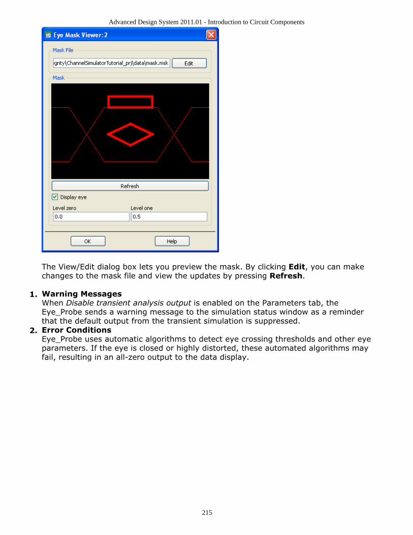
Advanced Design System 2011.01 - Introduction to Circuit Components
215
The View/Edit dialog box lets you preview the mask. By clicking Edit, you can makechanges to the mask file and view the updates by pressing Refresh.
Warning Messages1.When Disable transient analysis output is enabled on the Parameters tab, theEye_Probe sends a warning message to the simulation status window as a reminderthat the default output from the transient simulation is suppressed.Error Conditions2.Eye_Probe uses automatic algorithms to detect eye crossing thresholds and other eyeparameters. If the eye is closed or highly distorted, these automated algorithms mayfail, resulting in an all-zero output to the data display.

Advanced Design System 2011.01 - Introduction to Circuit Components
216
I_Probe (Current Probe) Symbol
Parameters
Name Description Units Default
Mode Mode: 0 => short; (not used) None (0)
C DC block capacitance (transient only) None
L DC feed inductance (transient only) None
Gain Current gain None None
SaveCurrent Save branch current: yes or no None yes
wImax Maximum current (warning) None
Notes/Equations
The positive current flow direction is assumed to be from pin 1 to pin 2.1.To measure a branch current, an ammeter must be connected in that branch before2.performing the analysis.The following table lists the DC operating point parameters that can be sent to the3.dataset.Name Description Units
I Current A
The current sampled by I_Probe will have the following name in the dataset:4.<instance name>.i; for example: I_Probe1.i.This component has no default artwork associated with it.5.

Advanced Design System 2011.01 - Introduction to Circuit Components
217
OscPort2 (Differential Oscillator Port)
Symbol
Parameters
Name Description Units Default
Mode Oscillator mode: automatic, small signal loop gain, or large signal loopgain
None Automatic
V Initial guess at fundamental voltage (automatic mode only) None
Z Initial value for Z0, in ohms (all modes) Ohm 1.1
NumOctaves Number of octaves to search (automatic mode only) None 2
Steps Number of steps per search octave (automatic mode only) None 10
FundIndex Fundamental number for oscillator (automatic mode only) None 1
Harm Harmonic or fundamental for oscillator None 1
MaxLoopGainStep Maximum arc length continuation step size during loop-gain search(automatic mode only)
None None
FreqPlan Sweep plan for frequency (small and large signal loop gain modes only) None None
VinjPlan Sweep plan for injected loop voltage (large signal loop gain mode only) None None
Notes/Equations
This is a special device used for an oscillator analysis. Do not use more than one1.oscillator test element (OscTest, OscPort, OscPort2) in a circuit.NumOctaves specifies the total number of octaves over which the oscillator search is2.done. Half of the octaves are below the initial frequency and half are above. Forexample, if NumOctaves is 2, then the frequency search goes from Freq/2 to Freq 2.Steps sets the number of frequency points per octave that are used in the search. Fora high-Q oscillator, a large number of steps might be required.If a fundamental voltage V is not specified, the simulator first performs a small-signal3.AC analysis to determine the actual frequency and oscillation voltage.If V is specified, it represents an initial guess at the fundamental oscillator voltage atthe point where the OscPort is inserted. The initial guess for V should be as close tothe actual value as possible. An inaccurate value increases the simulation time andmight prevent convergence. If it is not known, don't specify it.This device can operate in one of three different modes. In automatic mode, it is4.similar to the OscPort device, and is used with the harmonic balance oscillatoranalysis to determine the oscillator frequency, large signal solution and optionallyphase noise. In small signal loop gain mode, it is similar to the OscTest device, and isused to perform a small signal analysis of the oscillator loop gain versus frequency.

Advanced Design System 2011.01 - Introduction to Circuit Components
218
In large signal loop gain mode, it is used to simulate the large signal nonlinear loopgain of the oscillator versus frequency and injected loop voltage.This device can be used for both single-ended and differential oscillator topologies.5.For single-ended oscillators, the negative pins of this element should be grounded.For differential oscillators, it should be connected differentially into the oscillator loop.Provided the circuit produces at least one complex conjugate pole pair in the right-6.half-plane over the frequency range tested, the analysis will determine the oscillationwaveform and amplitude. Proper probe placement and impedance can reduce theanalysis time significantly and help ensure accurate oscillator analysis results. Toreduce the probability of a failed analysis, place the probe and set the initialimpedance in a manner consistent with the following guidelines:Feedback Oscillators (such as Colpitts)
Insert probe at a point in the feedback loop where the signal is contained to asingle path.Point the arrow of the probe in the direction of positive gain around the loop.Insert probe at a point in the feedback loop where source impedance is muchsmaller than load impedance (at least a factor of 10; a factor of 100 or more ispreferable).Point the arrow of the probe at the high impedance (load) node.Set the initial probe impedance (Z0) to a value approximately half-way betweenthe source and load impedances presented by the circuit at the point ofinsertion.To minimize the analysis time, set the probe impedance to a factor of 10 belowthe load impedance, and a factor of 10 above the source impedance (providedthe source and load impedances are sufficiently far apart). Doing this effectivelyreduces to zero the dependence of the small signal loop gain on Z0.
Negative Resistance OscillatorsInsert probe between a negative and positive impedance in the circuit. Thereshould be no other signal paths between these two parts of the circuit. Typically,the probe is inserted between the resonator and the effective negativeresistance.You can point the arrow of the probe at either the negative impedance node orthe positive impedance node.Set the initial probe impedance to any reasonable value. To minimize theanalysis time, it should be at least a factor of two higher or lower than themagnitude of the passive load impedance.The frequency is specified on the harmonic balance analysis component. Thevalue for Z is chosen based on impedance levels in the circuit and the degree ofnon-linearity in the circuit. Do not use either 1 or 0 for Z as this will causeconvergence problems.If the oscillator analysis fails, and this test indicates that the circuit shouldoscillate, the failure may be due to the fact that the circuit is too nonlinear. Thisproblem can sometimes be solved by trying different impedance values ofOscPort (determined by the Z attribute). Lower impedance values usually seemto work better. Also try reversing the OscPort direction.Another approach is to try to get the oscillator to oscillate at some nicerparameter value and then to sweep the parameter value to the desired value.The parameter may be bias, self-bias impedance, some gain controlling value,or another factor. In short, anything that will make the oscillator more linear,yet still let it oscillate.FundIndex is used for selecting which fundamental tone is considered theunknown frequency during oscillator analysis.The FundIndex default is 1, which means that Freq[1] on the Harmonic Balance
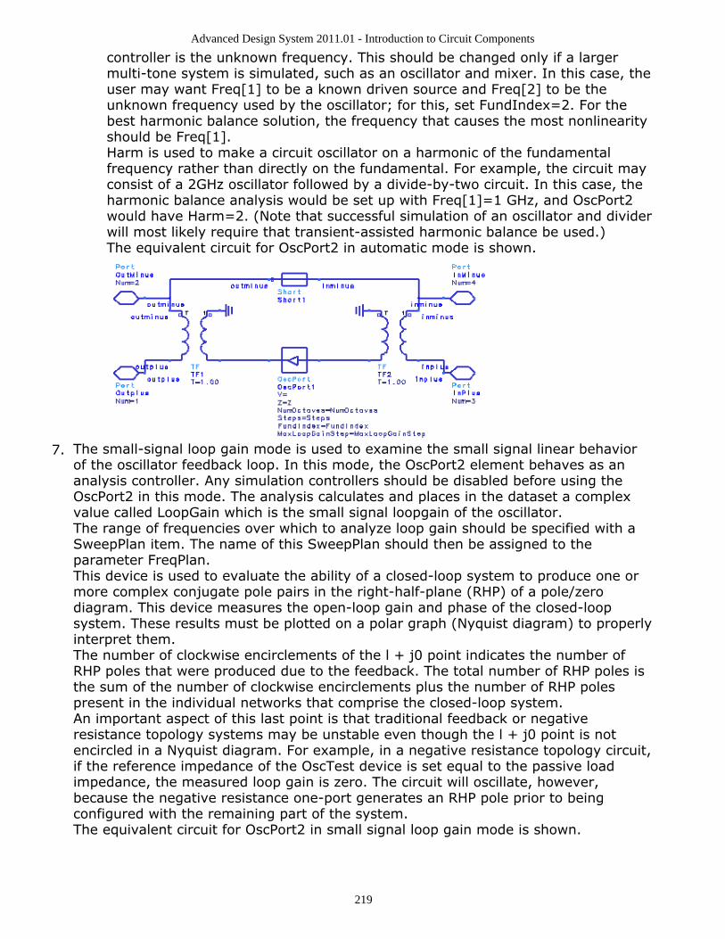
Advanced Design System 2011.01 - Introduction to Circuit Components
219
controller is the unknown frequency. This should be changed only if a largermulti-tone system is simulated, such as an oscillator and mixer. In this case, theuser may want Freq[1] to be a known driven source and Freq[2] to be theunknown frequency used by the oscillator; for this, set FundIndex=2. For thebest harmonic balance solution, the frequency that causes the most nonlinearityshould be Freq[1].Harm is used to make a circuit oscillator on a harmonic of the fundamentalfrequency rather than directly on the fundamental. For example, the circuit mayconsist of a 2GHz oscillator followed by a divide-by-two circuit. In this case, theharmonic balance analysis would be set up with Freq[1]=1 GHz, and OscPort2would have Harm=2. (Note that successful simulation of an oscillator and dividerwill most likely require that transient-assisted harmonic balance be used.)The equivalent circuit for OscPort2 in automatic mode is shown.
The small-signal loop gain mode is used to examine the small signal linear behavior7.of the oscillator feedback loop. In this mode, the OscPort2 element behaves as ananalysis controller. Any simulation controllers should be disabled before using theOscPort2 in this mode. The analysis calculates and places in the dataset a complexvalue called LoopGain which is the small signal loopgain of the oscillator.The range of frequencies over which to analyze loop gain should be specified with aSweepPlan item. The name of this SweepPlan should then be assigned to theparameter FreqPlan.This device is used to evaluate the ability of a closed-loop system to produce one ormore complex conjugate pole pairs in the right-half-plane (RHP) of a pole/zerodiagram. This device measures the open-loop gain and phase of the closed-loopsystem. These results must be plotted on a polar graph (Nyquist diagram) to properlyinterpret them.The number of clockwise encirclements of the l + j0 point indicates the number ofRHP poles that were produced due to the feedback. The total number of RHP poles isthe sum of the number of clockwise encirclements plus the number of RHP polespresent in the individual networks that comprise the closed-loop system.An important aspect of this last point is that traditional feedback or negativeresistance topology systems may be unstable even though the l + j0 point is notencircled in a Nyquist diagram. For example, in a negative resistance topology circuit,if the reference impedance of the OscTest device is set equal to the passive loadimpedance, the measured loop gain is zero. The circuit will oscillate, however,because the negative resistance one-port generates an RHP pole prior to beingconfigured with the remaining part of the system.The equivalent circuit for OscPort2 in small signal loop gain mode is shown.

Advanced Design System 2011.01 - Introduction to Circuit Components
220
The large-signal loop gain mode is used to examine the behavior of the oscillator8.feedback loop as a function of frequency and injected voltage. It can be used toobserve the compression of loop gain as the loop voltage is increased. In this mode,the OscPort2 element behaves as an analysis controller. Any simulation controllersshould be disabled before using the OscPort2 in this mode. The analysis calculatesand places in the dataset a complex value called LoopGain which is the large signalloop gain of the oscillator. The circuit will sustain oscillation at the point at which themagnitude of LoopGain equals one and the phase of LoopGain equals zero.The range of frequencies over which to analyze loop gain should be specified with aSweepPlan item. The name of this SweepPlan should then be assigned to theparameter FreqPlan.The range of voltages over which to analyze loop gain should be specified with aSweepPlan item. The name of this SweepPlan should then be assigned to theparameter VinjPlan. Initially the sweep should be done with a logarithmic sweep todetermine where the oscillator loop goes into compression. Once this range isestimated, a linear sweep can be done to zero in north injected voltage that causesoscillation to be sustained.A useful way to interpret results from this analysis is to plot the phase of LoopGainagainst LoopGain in decibels. Lines of constant frequency will be plotted with valuesat each voltage value. The circuit will oscillate at the frequency and voltageassociated with the (0,0) point on the graph.The equivalent circuit for OscPort2 in large signal loop gain mode is shown.
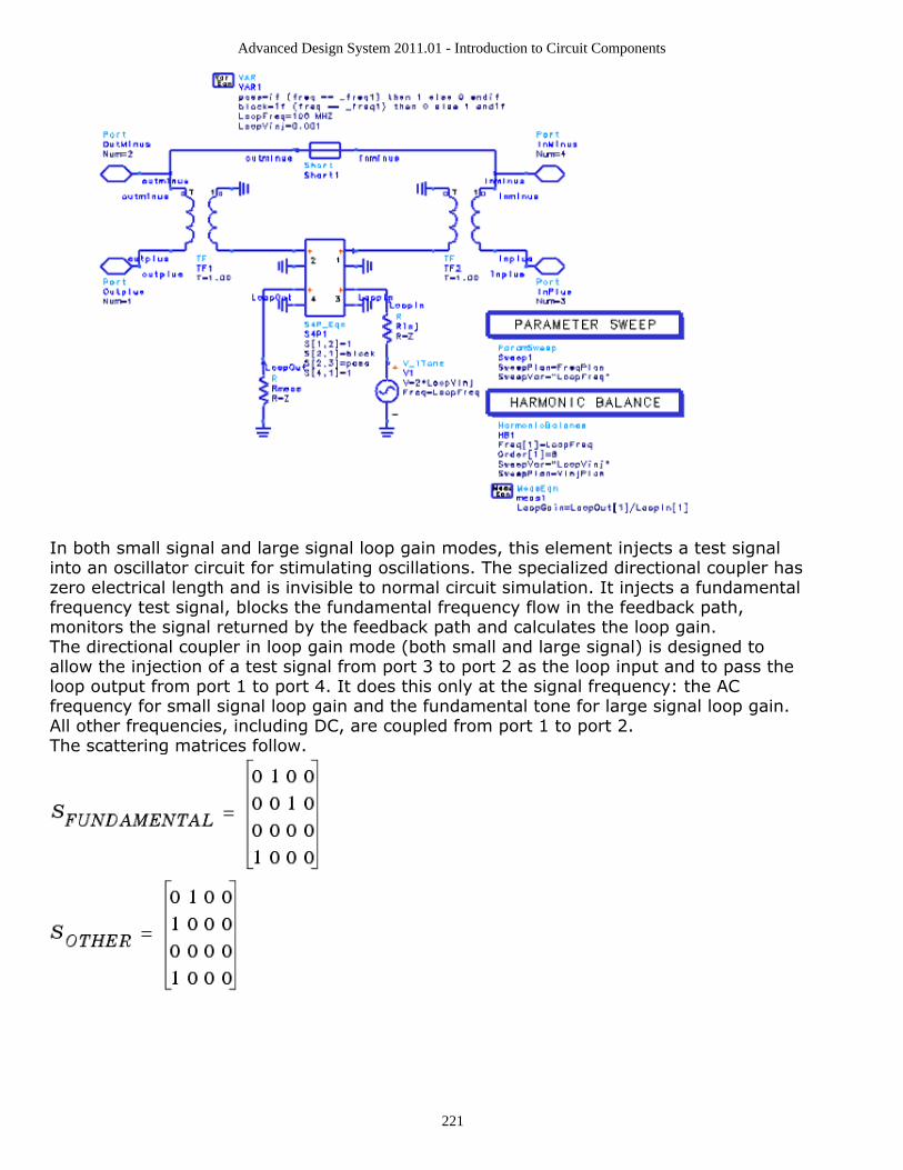
Advanced Design System 2011.01 - Introduction to Circuit Components
221
In both small signal and large signal loop gain modes, this element injects a test signalinto an oscillator circuit for stimulating oscillations. The specialized directional coupler haszero electrical length and is invisible to normal circuit simulation. It injects a fundamentalfrequency test signal, blocks the fundamental frequency flow in the feedback path,monitors the signal returned by the feedback path and calculates the loop gain.The directional coupler in loop gain mode (both small and large signal) is designed toallow the injection of a test signal from port 3 to port 2 as the loop input and to pass theloop output from port 1 to port 4. It does this only at the signal frequency: the ACfrequency for small signal loop gain and the fundamental tone for large signal loop gain.All other frequencies, including DC, are coupled from port 1 to port 2.The scattering matrices follow.

Advanced Design System 2011.01 - Introduction to Circuit Components
222
OscPort (Grounded Oscillator Port)
Symbol
Parameters
Name Description Units Default
V Initial guess at fundamental voltage None
Z Initial value for Z0 Ohm 1.1
NumOctaves Number of octaves to search None 2
Steps Number of steps per search octave None 10
FundIndex Fundamental number for oscillator None 1
Harm Harmonic or fundamental for oscillator None 1
MaxLoopGainStep Maximum arc length continuation step size during loop-gain search None None
Notes/Equations
This is a special device used for an oscillator analysis. Do not use more than one1.oscillator port in a circuit.NumOctaves specifies the total number of octaves over which the oscillator search is2.done. Half of the octaves are below the initial frequency and half are above. Forexample, if NumOctaves is 2, then the frequency search goes from Freq/2 toFreq × 2. Steps sets the number of frequency points per octave that are used in thesearch. For a high-Q oscillator, a large number of steps might be required.If fundamental voltage V is not specified, the simulator first performs a small-signal3.AC analysis to determine the actual frequency and oscillation voltage.If V is specified, it represents an initial guess at the fundamental oscillator voltage atthe point where the OscPort is inserted. The initial guess for V should be as close tothe actual value as possible. An inaccurate value increases the simulation time andmight prevent convergence. If it is not known, don't specify it.Provided the circuit produces at least one complex conjugate pole pair in the right-4.half-plane over the frequency range tested, the analysis will determine the oscillationwaveform and amplitude. Proper probe placement and impedance can reduce theanalysis time significantly and help ensure accurate oscillator analysis results. Toreduce the probability of a failed analysis, place the probe and set the initialimpedance in a manner consistent with the following guidelines:Feedback Oscillators (such as Colpitts)
Insert probe at a point in the feedback loop where the signal is contained to asingle path.Point the arrow of the probe in the direction of positive gain around the loop.Insert probe at a point in the feedback loop where source impedance is much

Advanced Design System 2011.01 - Introduction to Circuit Components
223
smaller than load impedance (at least a factor of 10; a factor of 100 or more ispreferable).Point the arrow of the probe at the high impedance (load) node.Set the initial probe impedance (Z0 ) to a value approximately half-way between
the source and load impedances presented by the circuit at the point ofinsertion.To minimize the analysis time, set the probe impedance to a factor of 10 belowthe load impedance, and a factor of 10 above the source impedance (providedthe source and load impedances are sufficiently far apart). Doing this effectivelyreduces to zero the dependence of the small signal loop gain on Z0.
Negative Resistance OscillatorsInsert probe between a negative and positive impedance in the circuit. Thereshould be no other signal paths between these two parts of the circuit. Typically,the probe is inserted between the resonator and the effective negativeresistance.You can point the arrow of the probe at either the negative impedance node orthe positive impedance node.Set the initial probe impedance to any reasonable value. To minimize theanalysis time, it should be at least a factor of two higher or lower than themagnitude of the passive load impedance.The frequency is specified on the harmonic balance analysis component. Thevalue for Z is chosen based on impedance levels in the circuit and the degree ofnon-linearity in the circuit. Do not use either 1 or 0 for Z as this will causeconvergence problems.If the oscillator analysis fails, and this test indicates that the circuit shouldoscillate, the failure may be due to the fact that the circuit is too nonlinear. Thisproblem can sometimes be solved by trying different impedance values ofOscPort (determined by the Z attribute). Lower impedance values usually seemto work better. Also try reversing the OscPort direction.Another approach is to try to get the oscillator to oscillate at some nicerparameter value and then to sweep the parameter value to the desired value.The parameter may be bias, self-bias impedance, some gain controlling value,or another factor. In short, anything that will make the oscillator more linear,yet still let it oscillate.FundIndex is used for selecting which fundamental tone is considered theunknown frequency during oscillator analysis.The FundIndex default is 1, which means that Freq[1] on the Harmonic Balancecontroller is the unknown frequency. This should be changed only if a largermulti-tone system is simulated, such as an oscillator and mixer. In this case, theuser may want Freq[1] to be a known driven source and Freq[2] to be theunknown frequency used by the oscillator; for this, set FundIndex=2. For thebest harmonic balance solution, the frequency that causes the most nonlinearityshould be Freq[1].Harm is used to make a circuit oscillator on a harmonic of the fundamentalfrequency rather than directly on the fundamental. For example, the circuit mayconsist of a 2GHz oscillator followed by a divide-by-two circuit. In this case, theharmonic balance analysis would be set up with Freq[1]=1 GHz, and OscPort2would have Harm=2. (Note that successful simulation of an oscillator and dividerwill most likely require that transient-assisted harmonic balance be used.)

Advanced Design System 2011.01 - Introduction to Circuit Components
224
OscTest (Grounded Oscillator Test)
Symbol
Parameters
Name Description Units Default
Port_Number Port number None 1
Z Port impedance Ohm 1.1
Start Start frequency GHz 1.0
Stop Stop frequency GHz 10.0
Points Number of frequency points None 101
Notes/Equations
This component performs an S-parameter analysis to evaluate the closed loop, small1.signal gain of a potential oscillator. It contains an analysis controller and sweeps thefrequency from Start to Stop. S(1,1) is the loop gain.This device is used to evaluate the ability of a closed-loop system to produce one or2.more complex conjugate pole pairs in the right-half-plane (RHP) of a pole/zerodiagram. This device measures the open-loop gain and phase of the closed-loopsystem. These results must be plotted on a polar graph (Nyquist diagram) to properlyinterpret them.The number of clockwise encirclements of the l + j0 point indicates the number ofRHP poles that were produced due to the feedback. The total number of RHP poles isthe sum of the number of clockwise encirclements plus the number of RHP polespresent in the individual networks that comprise the closed-loop system.An important aspect of this last point is that traditional feedback or negativeresistance topology systems may be unstable even though the l + j0 point is notencircled in a Nyquist diagram. For example, in a negative resistance topology circuit,if the reference impedance of the OscTest device is set equal to the passive loadimpedance, the measured loop gain is zero. The circuit will oscillate, however,because the negative resistance one-port generates an RHP pole prior to beingconfigured with the remaining part of the system.Another way of looking for potential oscillations is to look for the point(s) where the3.magnitude of the loop gain is greater than 1, phase is 0, and the phase is decreasingwith increasing frequency.If Port is set to 1 and S11 never goes outside the unity circle, the circuit will not4.
oscillate and the frequency search will fail. The circuit must be redesigned, or it willbe entered incorrectly. For the circuit to oscillate, the simulated loop gain must begreater than unity (1) when the phase is 0. If Port is set to 2, S22 is the S-parameter
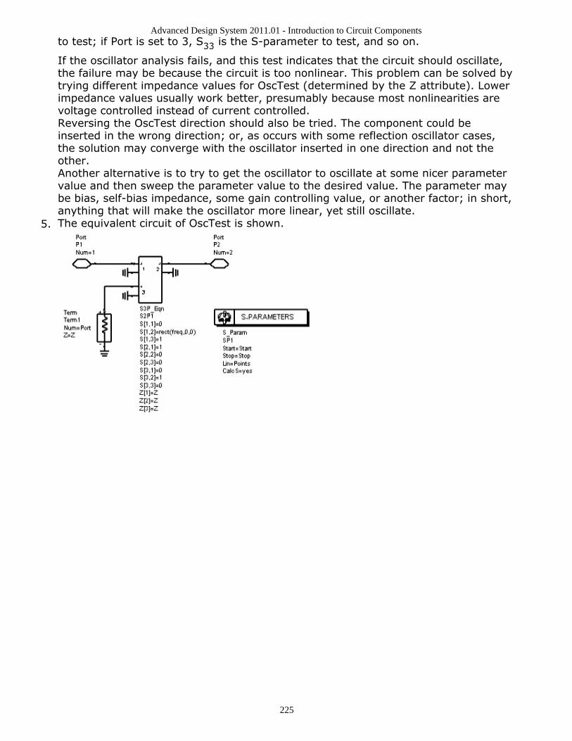
Advanced Design System 2011.01 - Introduction to Circuit Components
225
to test; if Port is set to 3, S33 is the S-parameter to test, and so on.
If the oscillator analysis fails, and this test indicates that the circuit should oscillate,the failure may be because the circuit is too nonlinear. This problem can be solved bytrying different impedance values for OscTest (determined by the Z attribute). Lowerimpedance values usually work better, presumably because most nonlinearities arevoltage controlled instead of current controlled.Reversing the OscTest direction should also be tried. The component could beinserted in the wrong direction; or, as occurs with some reflection oscillator cases,the solution may converge with the oscillator inserted in one direction and not theother.Another alternative is to try to get the oscillator to oscillate at some nicer parametervalue and then sweep the parameter value to the desired value. The parameter maybe bias, self-bias impedance, some gain controlling value, or another factor; in short,anything that will make the oscillator more linear, yet still oscillate.The equivalent circuit of OscTest is shown.5.

Advanced Design System 2011.01 - Introduction to Circuit Components
226
P_Probe2 (Differential Power Probe)
Symbol
Parameters
N/A
Notes/Equations
P_Probe2 measures dissipated power in DC, Transient, AC, HB, and Circuit Envelopesimulations. The probe samples current Ip through the terminal designated by the arrowsign and voltage Vp between the + and - terminals. Please refer to P Probe (GroundedPower Probe) (ccsim) for details about power computation.

Advanced Design System 2011.01 - Introduction to Circuit Components
227
P_Probe (Grounded Power Probe)
Symbol
Parameters
N/A
Notes/Equations
P_Probe measures dissipated power in DC, Transient, AC, HB, and Circuit Envelope. Theprobe samples current Ip through the pair of terminals designated by the arrow sign, andvoltage Vp from either of the terminals to ground.
For DC, AC, and HB simulations, the probe computes average power at each analysisfrequency f as:
If (f>0)
P = ½*Vp*conj(Ip) (1)
If (f=0)
P(0) = Vp*Ip (2)For transient simulations, the probe computes instantaneous power given by
p(t) = v(t)*i(t) (3)For Circuit Envelope, the probe computes instantaneous envelope power at eachharmonic, as given by eq. (1)-(2).The probe outputs 0 in SP simulations but it doesn't affect simulation results.The following table lists the measurement result that can be sent to the datasetName Description Units
p Power W

Advanced Design System 2011.01 - Introduction to Circuit Components
228
SP_Probe(S-Parameter Probe)
Symbol
Parameters
Name Description Units Default
Z Termination impedance Ohms 50.0
UsePorts Enables or disables the use of the ports specified using the L_Port and R_Portparameters. When this parameter is set to a value of 'no', the simulator will onlycalculate the S11 looking to the left and to the right of the probe. In other words allthe other ports will be ignored. When this parameter is set to a value of 'yes' thesimulator will calculate the S-Parameters taking into account the ports specified inthe parameters L_Port and R_Port.
None no
L_Port Left Looking Port (repeatable) None 1
R_Port Right Looking Port (repeatable) None 2
Notes/Equations
This component probes for the network parameters of the circuit when an S-1.Parameter analysis is performed.An example showing how to use the SP_Probe in S-parameter simulations is located2.in the SP_Probe_how_to_wrk. To access the example from the ADS Main window,select File > Open > Example > Tutorial > SP_Probe_how_to_wrk, then open thedesign A_readme. For information about this example, see Using SP_Probe in ADS(examples) in the Examples Documentation.When the initial DC operating point is performed, this component behaves like a3.short.Similarly when any other analysis besides the small signal S-Parameters is being4.performed, this component behaves just like a short.The network parameters that are computed are the S, Y and Z parameters.5.When the small signal noise analysis is performed, this component computes the6.Sopt, Rn, NF, NFmin, Te and Icor for the network.There will be 2 sets of network parameters, the first are the parameters looking to7.the left of the component and the second set are the parameters looking right.The port terminations used when computing the left looking parameters are specified8.using the parameter L_Port, and the termination numbers specified in the R_Portparameter will be used when computing the right looking parameters.The parameters L_Port and R_Port will only be used when the parameter UsePorts is9.set to yes.To clarify how the network parameters are saved, it is best to use the following10.
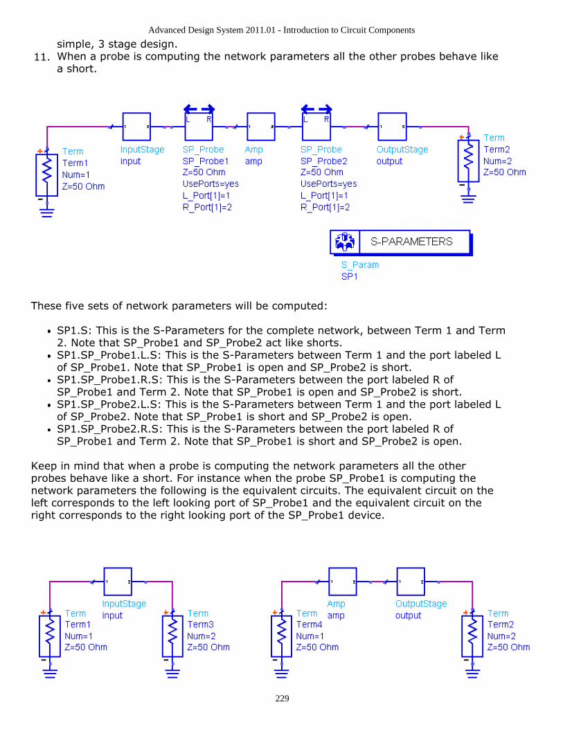
Advanced Design System 2011.01 - Introduction to Circuit Components
229
simple, 3 stage design.When a probe is computing the network parameters all the other probes behave like11.a short.
These five sets of network parameters will be computed:
SP1.S: This is the S-Parameters for the complete network, between Term 1 and Term2. Note that SP_Probe1 and SP_Probe2 act like shorts.SP1.SP_Probe1.L.S: This is the S-Parameters between Term 1 and the port labeled Lof SP_Probe1. Note that SP_Probe1 is open and SP_Probe2 is short.SP1.SP_Probe1.R.S: This is the S-Parameters between the port labeled R ofSP_Probe1 and Term 2. Note that SP_Probe1 is open and SP_Probe2 is short.SP1.SP_Probe2.L.S: This is the S-Parameters between Term 1 and the port labeled Lof SP_Probe2. Note that SP_Probe1 is short and SP_Probe2 is open.SP1.SP_Probe2.R.S: This is the S-Parameters between the port labeled R ofSP_Probe1 and Term 2. Note that SP_Probe1 is short and SP_Probe2 is open.
Keep in mind that when a probe is computing the network parameters all the otherprobes behave like a short. For instance when the probe SP_Probe1 is computing thenetwork parameters the following is the equivalent circuits. The equivalent circuit on theleft corresponds to the left looking port of SP_Probe1 and the equivalent circuit on theright corresponds to the right looking port of the SP_Probe1 device.

Advanced Design System 2011.01 - Introduction to Circuit Components
230
SProbe2 (SProbe2 Component) Symbol
Parameters
Name Description Units Default
Z0 Portimpedance
None 50
Notes/Equations
The SProbe2 component is used to determine small-signal impedances or reflection1.coefficients looking both directions (Z1 and Z2). These impedances may be used todetermine whether the conditions for oscillation are satisfied at any simulatedfrequency.This component can be inserted anywhere into a circuit without loading it.2.SProbe2 is intended to be used with the template SProbeT, which includes the3.SProbe2 component (in a Schematic, click Insert > Template > SProbeT).Do not combine the SProbe2 with other simulations that require Term components,4.including sources that have built-in Terms (e. g., P_1Tone).The equivalent circuit of SProbe2 is shown. When compared to the obsolete SProbe5.component, the SProbe2 circuit does not include the S-parameters and Sweep Plancontrollers. This is the only difference between them. It is intended that the S-parameters and Sweep Plan controllers be placed at the same level as the SProbe2component.

Advanced Design System 2011.01 - Introduction to Circuit Components
231
SProbePair2 (SProbePair2 Component) Symbol
Parameters
Name Description Units Default
Z0 Portimpedance
None 50
Notes/Equations
The SProbePair2 component is used to determine small-signal impedances or1.reflection coefficients looking both directions at the input and output planes of adevice or circuit. These impedances may be used to determine whether theconditions for oscillation are satisfied at any simulated frequency.This component can be inserted anywhere into a circuit without loading it.2.The SProbePair2 component is intended to be used with the template SProbePairT,3.which includes the SProbePair 2 component (in a Schematic, click Insert >Template > SProbePairT).Do not combine the SProbePair2 with other simulations that require Term4.components, including sources that have built-in Terms (e.g., P_1Tone).SProbePair2 is used in the following example:5.$HPEESOF_DIR/examples/MW_Ckts/MMIC_Amp_wrk/TwoStgAmpInZ_TBThe equivalent circuit of SProbePair2 is shown below. When compared to the obsolete6.SProbePair component, the SProbePair2 circuit does not include the S-parametersand Sweep Plan controllers. This is the only difference. It is intended that the S-parameters and Sweep Plan controllers be placed at the same level as theSProbePair2 component.

Advanced Design System 2011.01 - Introduction to Circuit Components
232
TimeDelta (Time Delta Component) Symbol
Parameters
Name Description Units Default
Direction1 Direction one None 1
Direction2 Direction two None 1
Thresh1 Threshold one V 0
Thresh2 Threshold two V 0
Scale Scale factor None 1e+6
Notes/Equations
TimeDelta generates an output voltage proportional to the time difference between1.two trigger points on two different baseband input voltage waveforms. The triggerpoints are user-defined by setting a threshold voltage and a slope. The slope can bespecified as either rising or falling by setting the direction parameter to a 1 or -1. Adirection parameter value of 0 is used if a trigger for either slope is desired.Only the baseband component of the input voltages are used to generate the2.triggers, so this model can be used in either envelope or transient time domainanalysis modes. Linear interpolation is used to estimate the actual trigger crossingtime to a finer resolution than the simulation time step.The input impedances are infinite. The output impedance is 1 ohm. The open circuit3.output voltage is equal to the time difference between the trigger2 and trigger1events, multiplied by the scaling factor. The output does not change until a trigger2event occurs and is held constant until another trigger2 event occurs. The scalingfactor is used so that the output voltages can be set to reasonable values (i.e., notnanovolts) which would often be less than the simulator's absolute convergencecriteria.Several example measurements possible with this model might be the input to output4.propagation delay of a circuit, the -40 to +20 dBm rise time of a demodulated RFpulse, various fall times, pulse widths, etc. The output voltage can be used for otherbehavioral models, for optimization, or for output to presentations.

Advanced Design System 2011.01 - Introduction to Circuit Components
233
TimeFrq (Time Frequency Component) Symbol
Parameters
Name Description Units Default
Direction Trigger Direction None 1
Thresh Trigger Threshold V 0
Scale Scale factor None 1e-6
Notes/Equations
TimeFrq generates an output voltage proportional to the inverse of the time between1.two consecutive triggers, which is basically the frequency of the triggering event. Thetrigger point is defined by setting a threshold voltage and a slope. The slope can bespecified as either rising or falling by setting the direction parameter to 1 or -1. Adirection parameter value of 0 is used if a trigger for either slope is desired.Only the baseband component of the input voltages is used to generate the trigger,2.so this model may be used in either envelope or transient time domain analysismodes. Linear interpolation is used to estimate the actual trigger crossing time to asignificantly higher resolution than the simulation time step.The input impedance is infinite. The output impedance is 1 ohm. The open circuit3.output voltage is equal to the inverse of the time difference between the last twotrigger events (i.e. the triggering frequency) multiplied by the scaling factor. Theoutput does not change until a trigger event occurs and is held constant until anotherevent occurs. The scaling factor is used so that the output voltage can be set toreasonable value which might otherwise be too large and affect the simulationaccuracy.
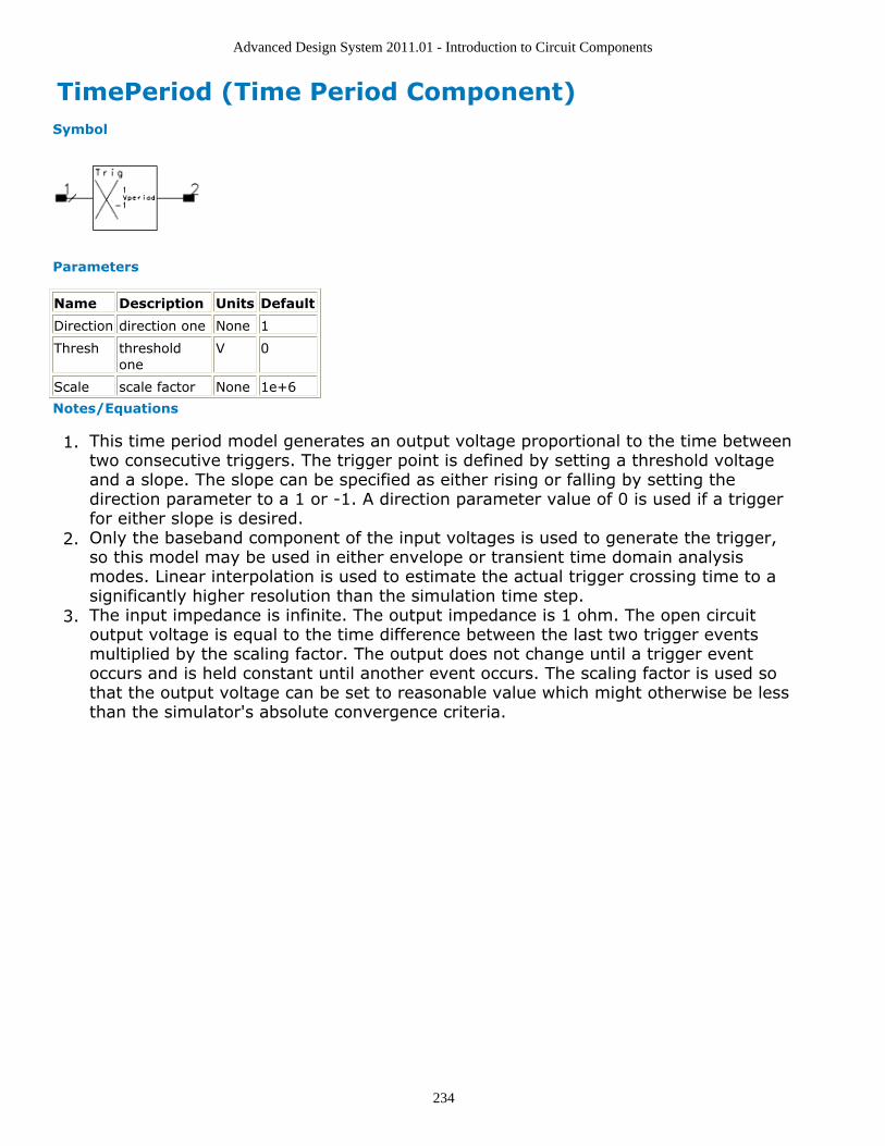
Advanced Design System 2011.01 - Introduction to Circuit Components
234
TimePeriod (Time Period Component) Symbol
Parameters
Name Description Units Default
Direction direction one None 1
Thresh thresholdone
V 0
Scale scale factor None 1e+6
Notes/Equations
This time period model generates an output voltage proportional to the time between1.two consecutive triggers. The trigger point is defined by setting a threshold voltageand a slope. The slope can be specified as either rising or falling by setting thedirection parameter to a 1 or -1. A direction parameter value of 0 is used if a triggerfor either slope is desired.Only the baseband component of the input voltages is used to generate the trigger,2.so this model may be used in either envelope or transient time domain analysismodes. Linear interpolation is used to estimate the actual trigger crossing time to asignificantly higher resolution than the simulation time step.The input impedance is infinite. The output impedance is 1 ohm. The open circuit3.output voltage is equal to the time difference between the last two trigger eventsmultiplied by the scaling factor. The output does not change until a trigger eventoccurs and is held constant until another event occurs. The scaling factor is used sothat the output voltage can be set to reasonable value which might otherwise be lessthan the simulator's absolute convergence criteria.

Advanced Design System 2011.01 - Introduction to Circuit Components
235
TimeStamp (Time Stamp Component) Symbol
Parameters
Name Description Units Default
Direction Direction one None 1
Thresh Threshold one V 0
Scale Scale factor None 1e+6
Notes/Equations
TimeStamp generates an output voltage proportional to the time that the last user-1.defined trigger occurred. The trigger point is defined by setting a threshold voltageand a slope. The slope can be specified as either rising or falling by setting thedirection parameter to a 1 or -1. A direction parameter value of 0 is used if a triggerfor either slope is desired.Only the baseband component of the input voltages is used to generate the trigger,2.so the model may be used in either envelope or transient time analysis modes. Linearinterpolation is used to estimate the actual trigger crossing time to a significantlyhigher resolution than the simulation time step domain.The input impedance is infinite. The output impedance is 1 ohm. The open circuit3.output voltage is equal to the time of the last trigger event multiplied by the scalingfactor. The output does not change until a trigger event occurs and is held constantuntil another event occurs. The scaling factor is used so that the output voltage canbe set to a reasonable value which might otherwise be less than the simulator'sabsolute convergence criteria.

Advanced Design System 2011.01 - Introduction to Circuit Components
236
WaveformStats (WaveformStats Component) Symbol
Parameters
none
Notes/Equations
This behavioral model can be used to measure the statistics of the baseband1.component of the input voltage. The inputs all have infinite input impedance; alloutputs are ideal voltage sources with zero output impedance.It calculates the running statistics of the signal since the last time reset went to 0;2.the reset signal should be high (1) for normal operation. The enable signal must behigh (1) for normal operation; it can be put in hold mode temporarily by bringing theenable signal to 0. The calculated running statistics are mean, standard deviation,minimum, maximum, sum, and number of samples of the input signal.If the enable is low during a reset, the accumulators are reset to 0; if the enable is3.high, then N is set to 1, and Sum is set equal to the input.In addition to making gated, statistical measurements for use in optimizations or4.presentations, you can use this device to model circuits such as ideal integrate-and-dump circuits or peak detector circuits.To measure the statistics of an RF carrier in circuit envelope mode, the correct5.demodulator must first be used to create a baseband voltage that can then be usedas an input to this device.This model operates in transient and envelope time domain analysis modes.6.The schematic example shows how this component works and a plot of the signals7.after simulating it.

Advanced Design System 2011.01 - Introduction to Circuit Components
237

Advanced Design System 2011.01 - Introduction to Circuit Components
238


![Circuit Components 1 G6 - CIRCUIT COMPONENTS [3 exam question - 3 groups] G6AResistors; capacitors; inductors G6BRectifiers; solid state diodes and transistors;](https://static.fdocuments.net/doc/165x107/56649ddc5503460f94ad3e5c/circuit-components-1-g6-circuit-components-3-exam-question-3-groups-g6aresistors.jpg)


![G6 - CIRCUIT COMPONENTS [3 exam question - 3 groups]](https://static.fdocuments.net/doc/165x107/56814a88550346895db79b3e/g6-circuit-components-3-exam-question-3-groups.jpg)

![G6 - Circuit Components 1 G6 - CIRCUIT COMPONENTS [3 exam question - 3 groups] G6A - Resistors; capacitors; inductors G6B - Rectifiers; solid state diodes.](https://static.fdocuments.net/doc/165x107/56649e755503460f94b75dea/g6-circuit-components-1-g6-circuit-components-3-exam-question-3-groups.jpg)