MANUFACTURING TECHNOLOGY UNIT – IV GEAR MANUFACTURING PROCESS.
Upload
vuongquynhCategory
view
217download
1
INTERNATIONAL TECHNOLOGY ROADMAP
FOR SEMICONDUCTORS
2001 EDITION
FACTORY INTEGRATION

TABLE OF CONTENTS Scope ....................................................................................................................... 1 Difficult Challenges ................................................................................................ 2
Complexity Management ................................................................................................. 3 Factory Optimization ........................................................................................................ 3 Extendibility, Flexibility, and Scalability (EFS) .................................................................. 3 Post Bulk CMOS Manufacturing....................................................................................... 5 450 mm Wafer Size Conversion....................................................................................... 5
Technology Requirements ..................................................................................... 6 Factory Operations .......................................................................................................... 6 Factory Operations Technology Requirements ................................................................ 7 Production Equipment...................................................................................................... 9 Production Equipment Technology Requirements...........................................................10 Material Handling Systems..............................................................................................13 Factory Information and Control Systems .......................................................................16 Facilities..........................................................................................................................19 Probe/Test Manufacturing...............................................................................................22
Potential Solutions ............................................................................................... 24 Factory Operations .........................................................................................................24 Production Equipment.....................................................................................................25 Material Handling Systems..............................................................................................26 Factory Information and Control Systems .......................................................................28 Facilities..........................................................................................................................29 Probe/Test Manufacturing...............................................................................................30
Crosscut Issues .................................................................................................... 30 Environmental, Safety and Health...................................................................................30 Assembly and Packaging................................................................................................31 Yield Management ..........................................................................................................31 Metrology Integration ......................................................................................................32 Static Charge Control......................................................................................................32 Factory Interface Standards Requirements .....................................................................33

LIST OF FIGURES Figure 44 a) Factory Integration Scope and b) Relationship between Thrusts and Difficult Challenges................................................ 2 Figure 45 Factory Operations Potential Solutions ........................................................ 24 Figure 46 Production Equipment Potential Solutions.................................................... 25 Figure 47 Material Handling Systems Potential Solutions............................................. 26 Figure 48 Factory Information and Control Systems (FICS) Potential Solutions ........... 28 Figure 49 Facilities Potential Solutions......................................................................... 29 Figure 50 Probe/Test Manufacturing Potential Solutions .............................................. 30 Figure 51 Integrated Factory Interface Standards ......................................................... 33
LIST OF TABLES Table 65 Factory Integration Difficult Challenges ............................................................ 4 Table 66a Factory Operations Technology Requirements—Near-term ........................... 7 Table 66b Factory Operations Technology Requirements—Long-term ........................... 8 Table 67a Production Equipment Technology Requirements—Near-term..................... 10 Table 67b Production Equipment Technology Requirements—Long-term .................... 11 Table 68a Material Handling Systems Technology Requirements—Near-term ............. 14 Table 68b Material Handling Systems Technology Requirements—Long-term ............. 15 Table 69a Factory Information and Control Systems Technology Requirements— Near-term[1]................................................................................................................... 18 Table 69b Factory Information and Control Systems Technology Requirements— Long-term[1]................................................................................................................... 18 Table 70a Facilities Technology Requirements—Near-term[1]...................................... 20 Table 70b Facilities Technology Requirements—Long-term[1] ..................................... 21 Table 71a Probe/Test Manufacturing Technology Requirements—Near-term............... 23 Table 71b Probe/Test Manufacturing Technology Requirements—Long-term............... 23 Table 72 Assembly and Packaging Potential Solutions ................................................. 31 Table 73 Yield Management Potential Solutions ........................................................... 32


Factory Integration 1
THE INTERNATIONAL TECHNOLOGY ROADMAP FOR SEMICONDUCTORS: 2001
FACTORY INTEGRATION1 SCOPE Realizing the potential of Moore’s Law requires taking full advantage of device feature size reductions, yield improvement to near 100%, wafer size increases, and other manufacturing productivity improvements. This in turn requires a factory that can fully integrate the production equipment that is the foundation to realizing Moore’s law and the ITRS with other factory components needed to efficiently produce the right products in the right volumes on schedule. Preserving the decades-long trend of 30% per year reduction in cost per function also requires capturing all possible cost reduction opportunities. To continue this pace requires the vigorous pursuit of the following fundamental manufacturing attributes: maintaining cost per unit area of silicon, decreasing factory ramp time, and increasing factory flexibility to changing technology and business needs. Contributors to this section
Moore’s Law and industry trends
Continuation of this remarkable record now faces several challenges that threaten to slow the industry’s growth, including:
1. Integrating increasingly complex factories—Rapid changes in semiconductor technologies, business requirements, and market conditions are making effective and timely factory integration to meet accelerated ramp and yield targets more difficult over time. The factory now must integrate an even larger number of new and different equipment types and software applications to meet multiple business objectives and customer requirements. Additional information on disruptive technology introductions
2. Production equipment OEE performance and extendibility—Production equipment is not keeping up with Overall Equipment Efficiency (OEE) and Availability targets which has an enormous impact on capital and operating costs. The industry is unable to effectively reuse equipment or skills due to the rapid introduction of new equipment (157 nm lithography) and materials (SOI, copper, high κ gate stack, low κ dielectrics, etc.).
3. Realizing 300 mm conversion efficiencies—The industry must quickly ramp 300 mm factory production to high volumes while achieving the efficiency targets that it has set. Some of these efficiencies include >2.25 more die per wafer than 200mm, >30% cost per die reduction, 100% AMHS interbay and intrabay systems for operational flexibility and cost improvements, and the ability to track and run different recipes for each wafer within a carrier for operational flexibility.
4. Post Bulk CMOS and 450 mm wafer manufacturing paradigms—The conversion to novel devices and 450 mm wafers represent key inflection points for semiconductor manufacturing. Novel devices beyond Bulk CMOS and their potential impacts to equipment and manufacturing are not well defined, but are expected to be significant. Conversion to 450 mm wafers represents another change opportunity to improve manufacturing cost effectiveness and will be an important factor in the semiconductor industry’s ability to continue realizing Moore’s law.
Key industry challenges
Dealing with these challenges means that some fundamental attributes of semiconductor manufacturing must be improved: maintaining or reducing cost per area of processed silicon, decreasing time to ramp a factory to high volume production with high yield, and increasing flexibility to adapt to new business conditions and models.
Cost per unit area of silicon - Manufacturing cost per unit area of silicon is a measure of productivity. The capital cost of a factory has grown significantly each year, from $50M in the 1980s to $2.7B in 2001.2 Improvements in equipment performance, continued high line and die yields, successful conversion to 300 mm wafer high volume production, continuous operating cost reductions, and cost effective incorporation of technology advancements will assure we continue this trend.
1 Factory integration is the combination of factory operations, production equipment, facilities, material handling, factory information and control systems, and probe/test manufacturing working in a synchronized way to profitably produce complex products for a time-sensitive market. 2 Strategies for determining or dealing with the upper limit of factory cost are beyond the scope of this chapter.

2 Factory Integration
THE INTERNATIONAL TECHNOLOGY ROADMAP FOR SEMICONDUCTORS: 2001
Time to ramp a factory to high volume production with high yields - Decreasing time to ramp a factory to high volume production and high yield has more economic impact than reducing operating costs. (For more information on Factory Ramp, Cost, and Yield model, view the supplemental files.) New factories must be built and ramped to mature production at a much faster rate as reflected in Tables 66 and 70. Existing factories must be upgraded faster without impacting ongoing production.
Increasing flexibility to accommodate technology and business changes - Technology advances and the globalization of manufacturing enterprises has led to a decrease in cost for electronic components. This enables new markets to open and creates the need to increase the pace of new product introduction. The flexibility to accommodate these changes in business expectations must improve without significant cost impacts.
High-volume factories historically push the manufacturing technology envelope and are the focus of the factory integration chapter. The differing requirements between high-product-mix and low-product-mix factories are also addressed.
As shown in Figure 44(a), a semiconductor factory extends across several manufacturing domains, which include wafer manufacturing or fabrication, chip manufacturing which includes probe/e-test, backgrind, and singulation, and finally product manufacturing where the final package is assembled and tested. Silicon substrate manufacturing and product distribution are outside the scope of factory integration.
While the integrated factory must meet the requirements stated above, these are more easily dealt with if partitioned into 5 thrusts, or functional areas, required to perform semiconductor manufacturing. The six thrusts are Factory Operations, Production Equipment, Material Handling, Factory Information and Control Systems, Facilities and Probe/Test Manufacturing. Factory Operations, and its associated factory business model, is a key driver of requirements and actions for the other thrusts. Overall, these thrusts are used to clarify how difficult challenges translate into technology requirements and potential solutions.
Figure 44 a) Factory Integration Scope and b) Relationship between Thrusts and Difficult Challenges
DIFFICULT CHALLENGES Difficult challenges associated with factory integration span multiple technology nodes and cut across the six factory thrust areas. Responses to these challenges are often linked to the technology introductions as a matter of industry convenience to minimize disruptions to operating factories. Near term difficult challenges for the factory include managing increasing complexity, continuously optimizing the factory as requirements change, and increasing its extendibility, flexibility, and scalability (EFS). Figure 44(b) illustrates the relationships between thrust areas and difficult challenges. Complexity Management is portrayed as a context for Factory Optimization and EFS.
Management of factory complexity - Complexity management means dealing with different factory process and product elements and their inter-relationships. As the number of these elements increases rapidly, management of factory complexity is becoming increasingly critical and more difficult.
(b) Relationship between Thrusts and Near Term Difficult Challenges
FactoryOperations FacilitiesProduction
EquipmentMaterialHandling
FactoryInformation
& ControlSystems
Maintain/reduce cost per unit areaAchieve ramp time reduction
Accommodate different business models
Probe/TestMfg
Complexity Management
Factory Optimization
Extendibility, Flexibility, Scalability
FactoryOperations FacilitiesFacilitiesProduction
EquipmentMaterialHandling
FactoryInformation
& ControlSystems
Maintain/reduce cost per unit areaAchieve ramp time reduction
Accommodate different business models
Maintain/reduce cost per unit areaAchieve ramp time reduction
Accommodate different business models
Probe/TestMfg
Complexity Management
Factory Optimization
Extendibility, Flexibility, Scalability
(a) Factory Integration Scope
WaferMfg
ChipMfg
ProductMfg
Dis
trib
utio
n
SiSu
bstr
ate
Mfg
The Factory
• Transistor Formation
• Interconnect
• Probe/Test• Backgrind• Singulation
• Packaging• Test
2001 Factory IntegrationRoadmap Scope
WaferMfg
ChipMfg
ProductMfg
Dis
trib
utio
n
SiSu
bstr
ate
Mfg
The Factory
• Transistor Formation
• Interconnect
• Probe/Test• Backgrind• Singulation
• Packaging• Test
2001 Factory IntegrationRoadmap Scope

Factory Integration 3
THE INTERNATIONAL TECHNOLOGY ROADMAP FOR SEMICONDUCTORS: 2001
Factory Optimization - Refers to the processes and procedures that enable sound and timely business decisions to be made in a resource-constrained environment. Such an environment demands rapid tradeoff decisions to optimize performance in the face of rapidly changing and uncertain business and technology conditions.
Factory extendibility, flexibility and scalability (EFS) - These relate to maximizing capital productivity and prolonging useful factory life. Factory extendibility (leveraging factory usage across several technology nodes), factory flexibility (adaptability to change), and factory scalability (inherent ability to increase the factory capacity) refer to the need for continuous and non-disruptive factory operation in the face of significant operational changes.
A summary of issues corresponding to these three near term Difficult Challenges is found in Table 65, with additional details discussed below. Refer to the supplemental links for more information on the Factory Integration Difficult Challenges.
COMPLEXITY MANAGEMENT Complexity is a measure of the combinations of interrelated physical and operational steps and interfaces required for the fabrication and delivery of semiconductor components. Such complexity arises from both external influences such as business and economic climate, and competitive pressures and internal influences such as decisions based on prevailing business models, technology opportunities, and legacy systems.
External factors include globalization of facilities and suppliers; changing business demands and business models; introduction of new technologies; and increasingly segmented and uncertain semiconductor markets. Internal factors include more complex processes; larger factories; integration of more process steps; and a higher degree of process and product mix within the factories. For example, the number of process steps needed to fabricate an IC is projected to more than double by 2012.
FACTORY OPTIMIZATION Factory operations optimization means meeting customer on-time delivery and product quality and reliability, while maintaining overall factory efficiency. This means minimizing variation, product cost per layer, and waste, scrap, and environmental impact. In addition, the factory must continue to provide a safe work environment; satisfy all local, state, and federal regulations; and demonstrate continuous improvement. Very often, such optimization requires choosing options that may conflict with one another.
Operational variance is a significant obstacle to optimizing factory operations. For example, reducing variation in equipment performance is a central issue as it affects yield, product reliability, planning, cycle time, customer delivery, overall factory effectiveness, and wafer cost. If equipment performance is inadequate then the risk of scrap or equipment unavailability increases, which results in an increase in on-time delivery variation and schedule slippage. Hence, one needs to identify, understand, evaluate, and minimize sources of variation to improve factory optimization capability.
Other factors inhibiting optimization include legacy system management, the lack of adequate data management capabilities and understanding of important cause-effect relationships, inadequate decision-making time, and conflicting polices or procedures.
Given a business model, a factory manager must make decisions involving tradeoffs and compromises under resource and time constraints. This is the fundamental reality of factory optimization, since there is never enough time, resources, nor information to eliminate the risk involved to make these choices.
EXTENDIBILITY, FLEXIBILITY, AND SCALABILITY (EFS) EFS relates to the need to extend the useful life of facilities, equipment and factory information and control systems under a widely varying set of business conditions.
Extendibility—Extendibility refers to prolonging the useful life of the factory across several process generations. The challenge is to introduce new technologies or business models into older factories with a minimum of new capital equipment, learning and training, while limiting major retrofits, re-engineering, and factory disruption.

4 Factory Integration
THE INTERNATIONAL TECHNOLOGY ROADMAP FOR SEMICONDUCTORS: 2001
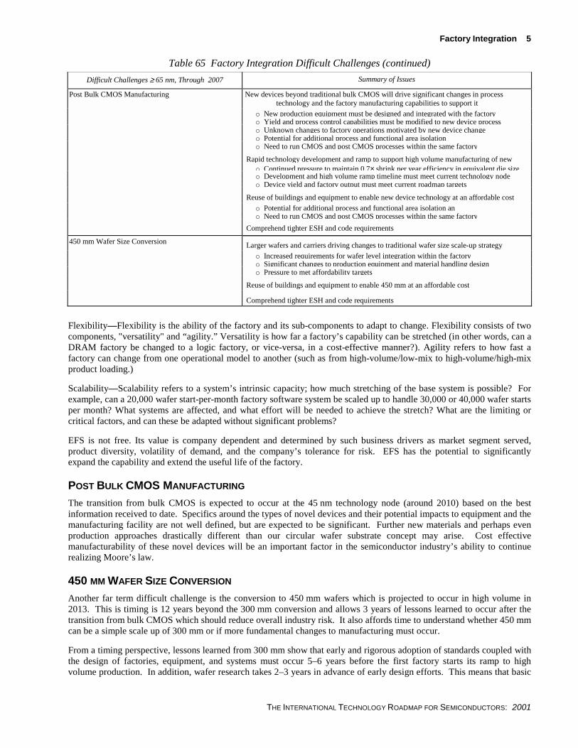
Table 65 Factory Integration Difficult Challenges Difficult Challenges=≥=65 nm, Through 2007 Summary of Issues
Complexity Management Rapid changes to business needs, demand, and globalization trends o Increasing rate of new product and technology introductions o Globally disparate factories run as single “virtual factory” o Need to meet regulations in different geographical areas o Effectively manage complex supply chains Increasing process and product complexity o Explosive growth of data collection/analysis requirements o Increasing number of processing steps including material movements o Multiple lots in a carrier and single wafer control/transport for an equipment group o Multiple Products on a wafer o Multiple package form factors Larger wafers and carriers driving ergonomic solutions o Increasing expectations for integrated material handling and software control systems Increased reliance on factory information and control systems o Multiple information and control system interdependencies o Standalone and Integrated Reliability required to keep factories operating o Co-existence of new factory information and control systems with existing (legacy) Pace of standards definition and implementation is not meeting factory integration needs Addressing complexity while keeping costs in perspective Factory Optimization Increased customer expectation to meet on time delivery o Balanced throughput and cycle time o Reduce time to ramp factories, products, and processes Increased urgency for improved factory effectiveness o Ability to measure effectiveness and adjust/optimize factory output High factory yield at startup o Reduce effects of parametric variation Reduce wafer and product cost Satisfy all domestic and international regulations Extendibility, Flexibility, and Scalability Reuse of building, production and support equipment, and factory information and control
systems o Across multiple technology nodes and wafer size conversions Factory designs that support rapid process and technology changes and retrofits o Understand up-front costs to incorporate EFS o Determine which EFS features to include and not to include o Minimize downtime to on-going operations Comprehend tighter ESH/Code requirements Comprehend increased purity requirements for process and materials
Factory Integration 5
THE INTERNATIONAL TECHNOLOGY ROADMAP FOR SEMICONDUCTORS: 2001
Table 65 Factory Integration Difficult Challenges (continued) Difficult Challenges=≥=65 nm, Through 2007 Summary of Issues
Post Bulk CMOS Manufacturing New devices beyond traditional bulk CMOS will drive significant changes in process technology and the factory manufacturing capabilities to support it
o New production equipment must be designed and integrated with the factory o Yield and process control capabilities must be modified to new device process o Unknown changes to factory operations motivated by new device change o Potential for additional process and functional area isolation o Need to run CMOS and post CMOS processes within the same factory Rapid technology development and ramp to support high volume manufacturing of new o Continued pressure to maintain 0.7× shrink per year efficiency in equivalent die size o Development and high volume ramp timeline must meet current technology node o Device yield and factory output must meet current roadmap targets Reuse of buildings and equipment to enable new device technology at an affordable cost o Potential for additional process and functional area isolation an o Need to run CMOS and post CMOS processes within the same factory Comprehend tighter ESH and code requirements
450 mm Wafer Size Conversion Larger wafers and carriers driving changes to traditional wafer size scale-up strategy o Increased requirements for wafer level integration within the factory o Significant changes to production equipment and material handling design o Pressure to met affordability targets Reuse of buildings and equipment to enable 450 mm at an affordable cost Comprehend tighter ESH and code requirements Flexibility—Flexibility is the ability of the factory and its sub-components to adapt to change. Flexibility consists of two components, "versatility" and “agility.” Versatility is how far a factory’s capability can be stretched (in other words, can a DRAM factory be changed to a logic factory, or vice-versa, in a cost-effective manner?). Agility refers to how fast a factory can change from one operational model to another (such as from high-volume/low-mix to high-volume/high-mix product loading.)
Scalability—Scalability refers to a system’s intrinsic capacity; how much stretching of the base system is possible? For example, can a 20,000 wafer start-per-month factory software system be scaled up to handle 30,000 or 40,000 wafer starts per month? What systems are affected, and what effort will be needed to achieve the stretch? What are the limiting or critical factors, and can these be adapted without significant problems?
EFS is not free. Its value is company dependent and determined by such business drivers as market segment served, product diversity, volatility of demand, and the company’s tolerance for risk. EFS has the potential to significantly expand the capability and extend the useful life of the factory.
POST BULK CMOS MANUFACTURING The transition from bulk CMOS is expected to occur at the 45 nm technology node (around 2010) based on the best information received to date. Specifics around the types of novel devices and their potential impacts to equipment and the manufacturing facility are not well defined, but are expected to be significant. Further new materials and perhaps even production approaches drastically different than our circular wafer substrate concept may arise. Cost effective manufacturability of these novel devices will be an important factor in the semiconductor industry’s ability to continue realizing Moore’s law.
450 MM WAFER SIZE CONVERSION Another far term difficult challenge is the conversion to 450 mm wafers which is projected to occur in high volume in 2013. This is timing is 12 years beyond the 300 mm conversion and allows 3 years of lessons learned to occur after the transition from bulk CMOS which should reduce overall industry risk. It also affords time to understand whether 450 mm can be a simple scale up of 300 mm or if more fundamental changes to manufacturing must occur.
From a timing perspective, lessons learned from 300 mm show that early and rigorous adoption of standards coupled with the design of factories, equipment, and systems must occur 5–6 years before the first factory starts its ramp to high volume production. In addition, wafer research takes 2–3 years in advance of early design efforts. This means that basic

6 Factory Integration
THE INTERNATIONAL TECHNOLOGY ROADMAP FOR SEMICONDUCTORS: 2001
work must start around 2004 to hit a 2013 conversion timeline. Refer to the supplemental material for additional details on 450 mm wafer size conversion]
TECHNOLOGY REQUIREMENTS To evaluate the technology requirements needed to achieve the primary goals described above, and subsequently to identify potential solutions to the difficult challenges that must be met, one can regard the factory as comprising six integrated and complementary functional areas.
• = Factory operations cover the set of policies and procedures that are used to plan, monitor and control production within a factory.
• = Production equipment covers process and metrology equipment (including embedded controllers) and their interfaces to other factory elements.
• = Material handling systems covers transport, storage, identification, tracking and control of direct and indirect materials.
• = Factory information and control systems includes computer hardware and software, manufacturing execution and decision support systems, factory scheduling, control of equipment and material handling systems, and process control.
• = Facilities include the infrastructure of buildings, utilities, and monitoring systems.
• = Probe/Test manufacturing includes equipment and manufacturing processes to test wafers and chips Refer to this link for more information regarding the relationship between difficult challenges; technology requirements; and factory integration thrusts
FACTORY OPERATIONS Factory operations refers to the effective application of resources and integration of other facets of manufacturing such as, information system, material handling, equipment and ESH in order to maximize throughput, minimize cycle time, WIP and maintain lower operating cost.
The Factory Operations Technology Requirements table lists the high-level production metrics and their required improvement targets through time in order for a semiconductor factory to achieve competitive performance characteristics. The factory operational metrics are cycle time per mask level for hot lots and non-hot lots, lots per carrier, and wafer layers per day per headcount. These metrics are further segmented to differentiate between two kinds of factories: high volume, high mix and high volume, low mix. In addition, there are a set of factory ramp-up metrics: ground breaking to first tool move-in, first tool move-in to first full loop wafer out, technology node to technology node change over, and floor space effectiveness.
The performance characteristics of a factory that best defines its competitive posture will depend on a number of factors. For example, there is a well-established trade-off between cycle time and asset utilization, with higher asset utilization leading to higher cycle times. Thus, each factory must balance the value of lowering cycle time for the business segment(s) in which it participates versus the cost of the lower asset utilization. Similarly, a factory that has high mix and low volume will have operational characteristics and will need decision support tools that will be different than those for a factory that is low mix and high volume. Asset utilization is captured in the form of OEE and the guidance to OEE improvement is given in the Production Equipment technology requirement table.
Once the fundamental performance characteristics have been established for a factory, there is a continuing need for increased productivity. This increased productivity is reflected either in lower cycle times or in increased throughput for the same capacity investment.
These requirements are meant to provide guidance so that research can be better focused toward the innovations required to achieve these objectives. These innovations are envisioned to be in the form of new concepts, policies, models, algorithms, etc. These will be expressed in the form of software applications that would be developed and released to manufacturing. These software applications will be integrated into the overall factory information and control systems, either as decision support tools or as execution tools. These tools will help to drive factory productivity improvements to achieve Factory Operations objectives.

Factory Integration 7
THE INTERNATIONAL TECHNOLOGY ROADMAP FOR SEMICONDUCTORS: 2001
The Factory Operations potential solutions are classified into planning decision support (DS) tools at the strategic level and tools for running the factory at the tactical or execution level. The solution components for these two levels are quite different. The tactical tools need quick access to transactional data where as the DS tools need large sets of data with several analysis/ reporting options. Some of the potential solutions are common to both 300 mm and 450 mm wafers.
One potential solution is tools (algorithms, models) for demand planning. Demand planning has become one of the most critical challenges facing semiconductor manufacturers. Demand information propagated over the factory network (Fab/Sort/Assembly/Test) is neither accurate nor responsive, which results in poor factory and supply chain planning. Successful determination of where, when and in what quantities the products are needed is essential for improving manufacturing productivity. The cost of capital equipment is significantly increasing and now constitutes more than 75% of wafer fab capital cost and via depreciation a significant fraction of the fixed operating costs as well. Reducing the impact of these increasing costs on overall wafer costs requires improvements in overall equipment efficiencies (OEE). Effective factory scheduling also plays a key role in improving OEE and it also leads to improved cycle time and On-Time-Delivery (OTD). In order to effectively utilize the expensive production equipment, it is imperative that effective scheduling and dispatching tools be utilized. Several factors complicate fab scheduling. These include AMHS that is not fully integrated with lot scheduling tools as well as scheduling policies that are not effectively integrated into lot scheduling tools. A real-time scheduling and dispatching tool integrated with AMHS and incorporating PM scheduling, and resource scheduling policies is required to reduce WIP, improve OTD and increase OEE. (Refer to additional details on Factory Operations technology requirements and potential solutions).
FACTORY OPERATIONS TECHNOLOGY REQUIREMENTS Table 66a Factory Operations Technology Requirements—Near-term
YEAR OF PRODUCTION 2001 2002 2003 2004 2005 2006 2007
DRAM ½ PITCH (nm) 130 115 100 90 80 70 65 MPU / ASIC ½ PITCH (nm) 150 130 107 90 80 70 65 MPU PRINTED GATE LENGTH (nm) 90 75 650 53 45 40 35 MPU PHYSICAL GATE LENGTH (nm) 65 53 45 37 32 28 25 WAFER DIAMETER 300 mm 300 mm 300 mm 300 mm 300 mm 300 mm 300 mm
High Volume / Low Mix Factory Requirements [4, 5]
Factory cycle time per mask layer (non-hot lot) [1,2] (days) 1.4 1.4 1.4 1.3 1.3 1.3 1.2
Factory cycle time per mask layer (hot lot) [1,2,7] (days) 1 1 1 0.9 0.9 0.9 0.8
Number of lots per carrier (lot) One One One One One One One Wafer layers/day/head count 55 55 55 61 61 61 67 High Volume / High Mix Factory Requirements [4, 5, 6]
Factory cycle time per mask layer (non-hot lot) [2,3] (days) 1.2 1.2 1.2 1.1 1.1 1.1 1
Factory cycle time per mask layer (hot lot) [2,3,7] (days) 0.75 0.75 0.75 0.65 0.65 0.65 0.55
Number of lots per carrier (lot) Multiple Multiple Multiple Multiple Multiple Multiple MultipleWafer layers/day/head count 37 37 37 41 41 41 45

8 Factory Integration
THE INTERNATIONAL TECHNOLOGY ROADMAP FOR SEMICONDUCTORS: 2001
Table 66a Factory Operations Technology Requirements—Near-term (continued) YEAR OF PRODUCTION 2001 2002 2003 2004 2005 2006 2007
DRAM ½ PITCH (nm) 130 115 100 90 80 70 65 MPU / ASIC ½ PITCH (nm) 150 130 107 90 80 70 65 MPU PRINTED GATE LENGTH (nm) 90 75 650 53 45 40 35 MPU PHYSICAL GATE LENGTH (nm) 65 53 45 37 32 28 25 WAFER DIAMETER 300 mm 300 mm 300 mm 300 mm 300 mm 300 mm 300 mm
Common requirements across Both Factory Types
Groundbreaking to first tool move-in (months) 9 9 9 8 8 8 7
First tool move-in to first full loop wafer out (months) 4 3.5 3.5 3 3 2.5 2.5
Node to Node change-over (weeks) 13 13 13 12 12 12 11 Floor space effectiveness 1X 1X 1X 1X 1X 1X 1X
Table 66b Factory Operations Technology Requirements—Long-term YEAR OF PRODUCTION 2010 2013 2016
DRAM ½ PITCH (nm) 45 32 22 MPU / ASIC ½ PITCH (nm) 45 32 22 MPU PRINTED GATE LENGTH (nm) 25 18 13 MPU PHYSICAL GATE LENGTH (nm) 18 13 9 WAFER DIAMETER 300 mm 450 mm 450 mm
High Volume / Low Mix Factory Requirements [4, 5]
Factory cycle time per mask layer (non-hot lot) [1,2] (days) 1.1 1.05 1
Factory cycle time per mask layer (hot lot) [1,2,7] (days) 0.7 0.65 0.6
Number of lots per carrier (lot) One One One Wafer layers/day/head count 73 81 89 High Volume / High Mix Factory Requirements [4, 5, 6]
Factory cycle time per mask layer (non-hot lot) [2,3] (days) 0.9 0.95 0.8
Factory cycle time per mask layer (hot lot) [2,3,7] (days) 0.45 0.4 0.35
Number of lots per carrier (lot) Multiple Multiple Multiple Wafer layers/day/head count 49 54 60 Common requirements across Both Factory Types
Groundbreaking to first tool move-in (months) 6 5.5 5
First tool move-in to first full loop wafer out (months) 2 1.5 1
Node to Node change-over (weeks) 10 9.5 9 Floor space effectiveness 1X 1X 1X
White—Manufacturable Solutions Exist, and Are Being Optimized
Yellow—Manufacturable Solutions are Known
Red—Manufacturable Solutions are NOT Known

Factory Integration 9
THE INTERNATIONAL TECHNOLOGY ROADMAP FOR SEMICONDUCTORS: 2001
Notes for Table 66a and b: [1] Assume number of hot lots in the factory is less than 2% of all lots
[2] Average number of wafers per hot lot ranges between 5 and 10
[3] Assume number of hot lots in the factory is less than 10% of all lots
[4] Assumes variable number of wafers per lot
[5] High volume is ~ 20K WSPM (all product wafers combined)
[6] High mix is at least 5 large volume products (product flows) with no one product has >50% of production volume
[7] Hot lot cycle time at 50% of non hot lot Explanation of Items for Factory Operations Technology Requirements: Explanation of Items Item Explanation Factory cycle time per mask layer (non-hot lot) [1,2]
Assume 25 (variable) wafers per lot. For example, if a process has 20 masking layers, and cycle time per mask layer is 1.5, then total factory (fabrication) cycle time is 20x1.5 = 30 days. A key metric of time to money.
Factory cycle time per mask layer (hot lot) [1,2,7]
Same definition as of above. Factories typically prioritize these lots over conventional lots, sometimes hold tools downstream to rapidly move them through the process flow and may also reduce metrology steps and sampling rates. As a result, the cycle time for hot lots are < 50% of non-hot lots. Assume 5-10 wafers per lot.
Number of lots per carrier Number of lots in each carrier that needs to be tracked, monitored, and processed at each production equipment. It impacts the extent of "recipe cascading" which enables production equipment to run in a continuous (non-stop) mode between lots in the same carrier and between sequential carriers.
Wafer layers/day/head count Measure of productivity which includes equipment output and direct labor staffing .Equation = total wafer processed per day in the factory x # of litho mask layers/total # of direct labor employees per day.
Groundbreaking to first full tool move-in
Time in months measured from groundbreaking to first move-in to the fab. Assumes site availability and all contract permits approved
First tool move-in to first full loop wafer out
A key metric of new factory ramp-up time. This is the time elapsed in months from first tool move-in to first full loop wafer out.
Node to Node change-over time The time in weeks for a new product or process to be implemented in a working factory (production equipment move-in to first lot out). About 80% of the current equipment is reused and 20% is new. Equipment already in place or available and may need to be qualified. Furnace and wet process equipment are not replaced. Not serial #1 equipment.
Floor space effectiveness This is a measure of equipment installation density in the cleanroom, and drives the requirement for the smallest footprint and the fastest run rate for production equipment. Equation = (# of Processing steps in the fab * WSPM/(Floor space area*30days). For every major node, one additional metal layer is added, and assuming a 4% increased run-rate improvement each year (by reduced processing time per wafer), the best that can be mathematically achieved is getting the same output per sq. meters of cleanroom for each new node.
PRODUCTION EQUIPMENT The scope of production equipment section includes all process and metrology equipment in the factory. Also included are tool embedded controllers, front-end module (EFEM) and loadports for carrier and wafer handling, software and firmware interfaces to host systems, and all facilities interfaces of the equipment.
Effective design and control of production equipment is central to controlling the cost of processing each unit area of silicon. The industry’s growth rate will not be sustainable in the future, if increasing capitalization cost trends continue without significant improvement in productivity. There are several factors which impact productivity of the equipment. They include: 1. Finding breakthrough solutions for increasing equipment reliability, availability and utilization, and overall
equipment effectiveness (OEE) 2. Reducing variation within and between equipment and attaining chamber and tool matching 3. Improving inter-operability and exchangeability by improving compliance to physical and data interface standards 4. Extending equipment lifetime to support multiple technology generations or nodes 5. Achieving more effective use of utilities and consumables, including reduction of non-product wafers, while
simultaneously reducing environmental impacts 6. Reducing “relative or normalized equipment capital cost” (rate at which equipment cost increases vis-à-vis
requirements for process capability) by speeding up the processing rate. This will drive reduced Cost of Ownership.

10 Factory Integration
THE INTERNATIONAL TECHNOLOGY ROADMAP FOR SEMICONDUCTORS: 2001
The Production Equipment potential solutions are prioritized towards attaining the improvements listed above. Equipment standards and interoperability solutions directly enable cost reduction of tools. OEE improvements can be achieved by innovative solutions in the area of in-situ monitoring, advance process control capability, smarter embedded controllers, self- diagnostics, remote diagnostic capability, and single wafer level tracking and control. More efficient equipment designs are achieved through the use of higher efficiency power distributions systems within the tool, more efficient tool heat load removal methods, and optimized recycling and reuse of water. Another high priority area is finding ways to extend the life of the equipment to support multiple technology nodes. Potential solutions to improve flexibility of the equipment to reduce cycle time and increase tool utilization will deliver much needed capabilities in carrier-level and wafer level integrated flow and controls. Other important areas are finding innovative solutions for ramp-up cycle time reduction and spares cost reduction. (Refer to additional details on Production Equipment technology requirements and potential solutions. Link to additional details on Agile Manufacturing and e-Manufacturing potential solutions.)
PRODUCTION EQUIPMENT TECHNOLOGY REQUIREMENTS Table 67a Production Equipment Technology Requirements—Near-term
YEAR OF PRODUCTION 2001 2002 2003 2004 2005 2006 2007 DRAM ½ PITCH (nm) 130 115 100 90 80 70 65 MPU / ASIC ½ PITCH (nm) 150 130 107 90 80 70 65 MPU PRINTED GATE LENGTH (nm) 90 75 650 53 45 40 35 MPU PHYSICAL GATE LENGTH (nm) 65 53 45 37 32 28 25 WAFER DIAMETER 300 mm 300 mm 300 mm 300 mm 300 mm 300 mm 300 mm
Throughput improvement (run-rate) per year (reduced process time per wafer) Base
4% faster than
previous year
4% faster than
previous year
New base
4% faster than
previous year
4% faster than
previous year
New base
Relative consumables, gases, chemicals, exhaust, emissions, and utilities
<1.0×××× of 200mm →→→→[8] →→→→
10% less of
previous node
→→→→ →→→→ 10% less
of previous
node Bottleneck production equipment OEE [3] 75% 78% 80% 82% 84% 87% 88% Average production equipment OEE [3] 55% 58% 60% 63% 65% 67% 70%
Relative maintenance and spares cost <1.0×××× of 200mm →→→→ →→→→
<98% of previous
node →→→→ →→→→
<98% of previous
node Overall factory non-product wafer usage (per wafer start) as a % of production <16% <15% <14% <13% <12% <11% <11%
% capital equipment reused from previous node Limited reuse [7] >90% >90% >90% >90% >90% >90%
Wafer edge exclusion [4] 2mm 2mm 2mm 2mm 2mm 2mm 2mm Production equipment lead time [5] from:
- Order to move-in (Litho)
12 mos 12 mos 12 mos 12 mos 12 mos 12 mos 12 mos
- Order to move-in (all others tools)
6 mos 6 mos 6 mos 6 mos 6 mos 6 mos 6 mos
- Setup to full throughput capable 4 wks 4 wks 4 wks 4 wks 4 wks 4 wks 4 wks Process/product changeover time (weeks) 4 4 4 3 3 3 2 Production equipment install and qualification cost as % of its capital cost 10% 8% 8% 6% 6% 6% 6%
Process equipment availability [6] >85% >88% >90% >92% >94% >95% >95% Metrology equipment availability [6] >90% 92% 94% >95% 95% >96% >97% Number of process recipes per wafer 1 1 1 1 1 1 1 Maximum allowable electrostatic field on wafer and mask surfaces (V/cm) 150 150 100 100 75 75 50
Relative capital cost [1] of production equipment <1.3x of 200mm
[2] → →→→→ New
base →→→→ →→→→ New base

Factory Integration 11
THE INTERNATIONAL TECHNOLOGY ROADMAP FOR SEMICONDUCTORS: 2001
Table 67b Production Equipment Technology Requirements—Long-term YEAR OF PRODUCTION 2010 2013 2016 DRAM ½ PITCH (nm) 45 32 22 MPU / ASIC ½ PITCH (nm) 45 32 22 MPU PRINTED GATE LENGTH (nm) 25 18 13 MPU PHYSICAL GATE LENGTH (nm) 18 13 9 WAFER DIAMETER 300 mm 450 mm 450 mm
Throughput improvement (run-rate) per year (reduced process time per wafer)
10–12% faster than
previous node
10–12% faster than
previous node
10–12% faster than
previous node
Relative consumables, gases, chemicals, exhaust, emissions, and utilities
10% less than
previous node
10% less than
previous node
10% less than
previous node
Bottleneck production equipment OEE [3] 90% 91% 92% Average production equipment OEE [3] 72% 74% 75%
Relative maintenance and spares cost <98% of previous
node
<120% of
previous node
<98% of previous
node
Overall factory non-product wafer usage (per wafer start) as a % of production <10% <9% <9%
% capital equipment reused from previous node >70% Limited reuse [7] >70%
Wafer edge exclusion [4] 2mm 2mm 2mm Production equipment lead time [5] from:
- Order to move-in (Litho)
12 mos 12 mos 12 mos
- Order to move-in (all others tools)
6 mos 6 mos 6 mos
- Setup to full throughput capable 4 wks 4 wks 4 wks Process/product changeover time (weeks) 2 2 2 Production equipment install and qualification cost as % of its capital cost 6% 8% 6%
Process equipment availability [6] >95% >95% >95% Metrology equipment availability [6] >98% >98% >98% Number of process recipes per wafer 1 1 1 Maximum allowable electrostatic field on wafer and mask surfaces (V/cm) 50 25 25
Relative capital cost [1] of production equipment New base
<1.3x of 300 mm
New base
White—Manufacturable Solutions Exist, and Are Being Optimized
Yellow—Manufacturable Solutions are Known
Red—Manufacturable Solutions are NOT Known
Notes for Table 67a and b: [1] Moore’s law implies 29% cost reduction per function per year. Lithography improvements contribute 15 to 20 % cost reduction per year. A significant part of the remainder must be made up by improvements in factory productivity through better operational efficiency, lower costs and cycle time reductions. This is very important for production equipment since it is the largest component of factory cost. [2] See References for a discussion of the basis for the 1.3 ratio. 3,4.
3 SEMATECH. I300I Factory Guidelines: Version 4.1. 97063311E-ENG. Austin, TX: SEMATECH. July 15, 1999.

12 Factory Integration
THE INTERNATIONAL TECHNOLOGY ROADMAP FOR SEMICONDUCTORS: 2001
[3] This is reused from 1998 Roadmap. 5
[4] This is relevant to basic equipment processing capability only. Exclusion includes both front and rear side of wafer. [5] This line is intended to drive increasingly better awareness of supply chain management. [6] Equipment availability includes all components. Examples: process chambers, load ports, wafer- handling systems, embedded controllers, mini-environment. [7] Reuse is extremely limited due to 200mm to 300 mm conversion at the 130 nm node. The same applies to the 300 mm to 450 mm at the 32 nm node.
[8] →= means that there is no change in the absolute value across the technology node.
Explanation of Items for Production Equipment Requirements Item Explanation Target throughput improvement (run-rate) per year (or reduced processing time per wafer)
Throughput improvements are achieved by reducing the processing time per wafer, and optimizing non-value added wafer handling and wafer-staging steps inside the equipment and by increasing the efficiency of the equipment embedded controller. Also eliminate any dead time between sequential wafer processing steps. E.g.,: if current run-rate is 100 wafers/hour, the required run-rate next year is (100 x 1.04) = 104 wafers/hour and (104 x 1.04)=108 wafers/hour the following year.
Relative consumables, exhaust, emissions, and utilities
For the 130 nm node, relative consumables are a ratio of (300 mm consumables/300 mm throughput in wafers per hour) divided by (200 mm consumables/200 mm throughput in wafers per hour). The same methodology applies for gases, chemicals, exhaust, emissions, and utilities. For the 90 nm node and beyond consumables is 90% of previous node assuming the same throughput. Global warming and general ESH initiatives may force additional tightening of this requirement.
Bottleneck production equipment OEE Overall equipment efficiency of the bottleneck production equipment. (Refer to SEMI E79 for OEE definition.) Bottleneck refers to the most constraint (limiting output) equipment in the factory.
Average production equipment OEE Overall equipment efficiency of the average production equipment. (Refer to SEMI E79 for OEE definition.) Relative equipment footprint For the 130 nm node, it is ratio of (300 mm equipment footprint/300 mm throughput in wafers per hour) divided
by (200 mm equipment footprint/200 mm throughput in wafers per hour). For the 90 nm node and beyond, footprint is 98% of previous node assuming the same throughput. [ Refer to SEMI E72. 6 The footprint used here infers to the cost footprint in the SEMI standard.]
Relative maintenance and spares cost For the 130 nm node, it is ratio of (300 mm maintenance and spares cost/300 mm throughput in wafers per hour) divided by (200 mm maintenance and spares cost/200 mm throughput in wafers per hour). For the 90 nm node and beyond it is 98% of previous node assuming the same throughput.
Overall factory non-product wafer usage (per wafer start)
Ratio of total non-production wafer consumption divided by total production wafer started for the same period. Typical non-product wafers include test wafers, monitor wafers, calibration wafers, dummy wafers. Consumption quantity includes both new and reused (reclaimed) non-product wafers.
% Capital equipment reused from previous technology node
% of capital (production) equipment quantity that is reused from node N to N+1. Example: if X number of production equipment of node N can be reused for node N+1 and the total number of production equipment for node N+1 is Y, then equipment reuse % is defined as X/Y.
Wafer edge exclusion Dimension in millimeters measured from wafer edge that is not used for printing saleable chips. Includes front and rear sides of wafer.
Production equipment lead time Time elapsed between when a purchase order has been placed for production equipment till the time the equipment has been qualified to run wafers at the quoted throughput (wafers per hour). Assume it is repeat order equipment, suppliers have sufficient mfg capacity, and learning achieved for fast install/qualification. For tools with long-lead items, risk reduction for equipment suppliers from order cancellation exposure may be mitigated by creative down-payment schemes.
Process/Product changeover time (in weeks)
Total time elapsed for old equipment move-out, new equipment move-in, install/hook-up and supplier qualification complete. Also assumes new equipment has space to move-in and major utility laterals are in place. Assume same wafer size, factory does not shut down and > 90% of existing equipment is reused.
Production equipment install & qualification cost as a % of capital equipment cost
Ratio of production equipment (installation cost + hook-up cost + qualification cost) divided by its upfront capital cost, expressed as a percentage. Equipment and facilities hook-up standardization will reduce this cost.
Process equipment availability Availability is 100% minus (scheduled downtime % + unscheduled downtime %) of the process (non-metrology) equipment. Scheduled downtime and unscheduled downtimes are defined in SEMI E10.
Metrology equipment availability Availability is 100% minus (scheduled downtime % + unscheduled downtime %) of the metrology equipment. Scheduled downtime and unscheduled downtimes are defined in SEMI E10.
4 Daniel Seligson, “The Economics of 300 mm Processing,” Semiconductor International, vol. 21, number 1, January 1998, pages 52-58. 5 Semiconductor Industry Association. “National Technology Roadmap for Semiconductors: 1998 Update.” Austin, TX:SEMATECH, 1999. 6 SEMI. E72-0699 – Provisional Specification and Guide for 300 mm Equipment Footprint, Height, and Weight.

Factory Integration 13
THE INTERNATIONAL TECHNOLOGY ROADMAP FOR SEMICONDUCTORS: 2001
Number of process recipes per carrier Indicates a requirement on all single wafer processing equipment to incorporate the ability to automatically change recipe and process parameters between any two wafers in a carrier and to do so in a continuous manner without interruption or manual intervention. Indicates the ability to process each wafer differently.
Maximum allowable electro static field on wafer and mask surfaces (V/cm)
Wafer and mask surface electric fields measured when they are removed from their carriers. Refer SEMI standards E78 and E43 for measurement methods.
Relative capital cost of production equipment
For 130 nm nodes, it is the ratio of (300 mm equipment capital cost/300 mm throughput in wafers per hour) divided by (200 mm equipment capital cost/200 mm throughput in wafers per hour). For the 90 nm node and beyond, capital cost is a new baseline, positively influenced by run-rate(wafers/hour) increases at each year.
MATERIAL HANDLING SYSTEMS Ergonomic and safety issues coupled with the need for efficient and rapid material transport will be the major drivers in defining material handling systems for the 300 mm wafer generation and beyond. The automated material handling systems must have acceptable Return on Investment (ROI) and must interface directly with all inline (i.e., used in normal process flow) production equipment. With the increase in 300 mm production equipment size, the utilization of floor space in the factory must improve. Solutions to provide higher wafer storage densities, short lead and install times, and better utilization of floor space through integration of process and metrology equipment must be developed.
Table 68 is based on the premise that as demands on the material handling system continues to increase, the drive toward combining interbay and intrabay transport function into one integrated capability, known as a direct or tool-to-tool transport system will be a reality. Over the next four years, material handling equipment/component failures must be reduced by 50%, while the time to repair each failure is similarly reduced. Throughput must be increased substantially and achieved with reduced delivery time. Furthermore, the material handling system needs to be designed so that it can accommodate the extendibility, flexibility, and scalability demands on the factory. New technology requirements were added to the roadmap this year to support the need for better wafer storage density, shorter lead and install times for material handling equipment, and increase in ease of extending an existing automated material handling system.
Concurrent with the drive towards direct transportation systems in 300 mm factories to transport WIP, IC makers, running high volume/high mix production will require automated transport for reticles in Reticle SMIF pods. For efficient production in such an environment, there will be a need to integrate WIP scheduling and dispatching systems with reticle storage and transport systems. It is expected that automated material handling systems for WIP and reticles will need to demonstrate similar performance characteristics. IC makers may choose different storage schemes in a reticle stocker. One case calls for bare reticle storage in the stocker and the other being stored in Reticle SMIF pods. Potential solutions for reticle transport systems must not negatively impact the litho equipment's footprint, run rate, and ease of installation or de-installation. The adoption of automated reticle transport systems by IC makers will depend on the business model employed at the factory. (Link to the Material Handling potential solutions table.) (Refer to supplemental files for additional details on Material Handling technology requirements and potential solutions.)

14 Factory Integration
THE INTERNATIONAL TECHNOLOGY ROADMAP FOR SEMICONDUCTORS: 2001
Table 68a Material Handling Systems Technology Requirements—Near-term YEAR OF PRODUCTION 2001 2002 2003 2004 2005 2006 2007 DRAM ½ PITCH (nm) 130 115 100 90 80 70 65 MPU / ASIC ½ PITCH (nm) 150 130 107 90 80 70 65 MPU PRINTED GATE LENGTH (nm) 90 75 650 53 45 40 35 MPU PHYSICAL GATE LENGTH (nm) 65 53 45 37 32 28 25 Material handling total capital cost as a % of total capital cost
< 3% [1]
< 3%
< 3%
< 2% [2]
< 2%
< 2%
< 2%
# Of transport system types within a factory 2 [3] 2 2 Some 1
and some 2
1 [4] 1 1
MTTR (minutes) (SEMI E10) 4 20 18 15 15 15 15 Failures per 24-hour day over total system (SEMI E10) <1 <1 <0.75 <0.5 <0.5 <0.5 <0.5
System throughput
• = Interbay transport (moves/hour) 1200 1300 1400 1500
• = Intrabay transport (moves/hour) 170 180 190 200
1625 [4] 1750 1875
Stocker cycle time (seconds) 15 15 14 12 12 10 10 Average factory wide carrier delivery time (in minutes) 10 10 10 8 5 5 5
Maximum factory wide carrier delivery time 20 20 20 15 15 15 15 Stocker storage density (% Total WIP carrier volume / Total stocker volume) [5]
Small stocker (%) >25 >30 >30 >40 >40 >40 >50
Nominal stocker (%) >30 >35 >35 >45 >50 >50 >60 Material handling equipment lead time (weeks) <16 <14 <12 <11 <10 <9 <8
Material handling equipment installation time (weeks) <8 <8 <7 <7 <6 <5 <4
System downtime required to extend system capacity when previously planned (minutes) [6]
<180 <90 <90 <60 <30 <30 <15
White—Manufacturable Solutions Exist, and Are Being Optimized
Yellow—Manufacturable Solutions are Known
Red—Manufacturable Solutions are NOT Known

Factory Integration 15
THE INTERNATIONAL TECHNOLOGY ROADMAP FOR SEMICONDUCTORS: 2001
Table 68b Material Handling Systems Technology Requirements—Long-term YEAR OF PRODUCTION 2010 2013 2016 DRAM ½ PITCH (nm) 45 32 22 MPU / ASIC ½ PITCH (nm) 45 32 22 MPU PRINTED GATE LENGTH (nm) 25 18 13 MPU PHYSICAL GATE LENGTH (nm) 18 13 9 Material handling total capital cost as a % of total capital cost
< 2%
< 3%
< 3%
# Of transport system types within a factory 1 1 1 MTTR (minutes) (SEMI E10) 12 10 8
Failures per 24-hour day over total system (SEMI E10) <0.5 <0.5 <0.3
System throughput
• = Interbay transport (moves/hour)
• = Intrabay transport (moves/hour)
2000 2000 2000
Stocker cycle time (seconds) 8 10 10
Average factory wide carrier delivery time (in minutes) 5 5 5
Maximum factory wide carrier delivery time 12 10 8 Stocker storage density (% Total WIP carrier volume / Total stocker volume) [5]
Small stocker (%)>50 >50 >50
Nominal stocker (%) >60 >60 >60 Material handling equipment lead time (weeks) <8 <8 <8 Material handling equipment installation time (weeks) <4 <4 <4 System downtime required to extend system capacity when previously planned (minutes) [6] 30 30 30
White—Manufacturable Solutions Exist, and Are Being Optimized
Yellow—Manufacturable Solutions are Known
Red—Manufacturable Solutions are NOT Known
Notes for Table 68a and b: [1] Year 2002—High throughput transportation [2] Year 2005—Direct transportation and fewer stockers [3] Interbay and intrabay transport system types [4] Single direct transport system [5] Required external maintenance access space is not included in these values. However, it is expected that required maintenance access, except for electrical power distribution access on the back, should be designed for internal to the stocker, with the proper clearance for entering/exiting the stocker. [6] These values are do not include downtimes associated with software upgrades, which are addressed by the Factory Information and Control Systems requirements (see Table 69) for unavailability of a mission critical application in a working factory due to install/upgrade (minutes) Explanation of Items for Material Handling Systems Requirements Item Explanation Material handling total capital cost as a % of total capital cost
Ratio of total capital cost of material (wafer and reticle, inter and intrabay) handling hardware divided by the total capital cost for production equipment and the building, expressed a percentage. For example, if the material handling cost is $30M, and the factory (capital equipment and building cost) is $1000M, then this ratio is 30/1000 = 3%.
Transport system types within a factory
Transport system types used in a factory for handling wafer carriers. Typically, today these are interbay and intrabay transport systems. In the future, there is a need to have one system that performs both the interbay and the intrabay transport functions. This does not mean one system from one supplier. This system maybe composed of interoperable sub-systems from multiple (best of breed) suppliers.
16 Factory Integration
THE INTERNATIONAL TECHNOLOGY ROADMAP FOR SEMICONDUCTORS: 2001
MTTR Mean Time To Repair, in minutes, for the fully integrated system. This means the mean unscheduled downtime (defined by SEMI E10) while repairing any system component.
Failures per 24 hour day (over total system)
Number of system component failures allowed throughout the system in a 24 hour day (or period). (Refer to SEMI E10 for more details on failure definition.)
System throughput Number of material handling moves per hour by the sub-system as defined below. Note that stocker robot moves from/to load ports are not assumed concurrent with nor included in system throughput moves
Interbay transport (moves/hour) Number of material handling moves per hour performed by the interbay transport system. An interbay transport move is defined as a carrier move from the loading of an interbay vehicle at a stocker interbay port to the unloading of the same vehicle at the destination stocker.
Intrabay transport (moves/hour) Number of material handling moves per hour performed by an intrabay transport loop. An intrabay transport move is defined as a carrier move from a stocker storage bin to a production equipment load port.
Stocker cycle time Time required, in seconds, for the stocker internal robot to move to a carrier at a port or storage bin, pickup the carrier, and deliver it to another port or storage bin within the same stocker.
Factory-wide carrier delivery time Time required, in minutes, to transport a carrier from one production equipment to any other production equipment in the factory. The time begins at the request for carrier movement and ends when the carrier arrives at the load port of the receiving equipment. Maximum delivery time is considered the peak performance capability defined as the average plus two standard deviations.
Stocker storage density (% Total WIP Carrier Volume/Total Stocker Volume)
Total WIP carrier volume that can be stored in a stocker divided by the total volume enclosed by the stocker, expressed as a percent (%). Carrier volume represented as a rectangular box enclosing all carrier handling features.
Small Stocker (%) Total WIP carrier volume that can be stored in a small stocker (defined as a stocker with capacity of 50 carriers or less) divided by the total volume enclosed by the small stocker, expressed as a percent.
Nominal Stocker (%) Total WIP carrier volume that can be stored in a Nominal stocker (defined as a stocker with capacity of 100 carriers) divided by the total volume enclosed by the nominal stocker, expressed as a percent.
Material Handling Equipment lead time (Weeks from order to move in)
Time elapsed, in weeks, between when a purchase order has been placed for a material handling system until the time the final system component is FOB at supplier’s dock. Based on size fab of approximately 200 meters by 80 meters, with 15-20 short bays. This lead time should not be affected by market demand on supplier.
Material Handling Equipment Installation time (Weeks from installation to full throughput capability)
Time elapsed, in weeks, between when the first component of the system is moved in from the dock until the final component is fully installed, started up, and tested to meet full designed through capability. Assume new factory and uninterrupted installation of the material handling system. Based on size fab of approximately 200 meters by 80 meters, with 15-20 short bays.
Ease of extending capacity Impact to material handling system, in terms of downtime minutes required for making connections to track extension or a new stocker. Adding new AMHS vehicles should require no system downtime.
System downtime required to extend system capacity when previously planned (minutes)
Impact to material handling system in terms of downtime, in minutes, of the material handling system, required for making connections to system track extensions or a new stocker when previsions for this expansion were incorporated in the original design.
FACTORY INFORMATION AND CONTROL SYSTEMS The scope of Factory Information and Control Systems (FICS) includes computer hardware and software, manufacturing execution and decision support systems, factory scheduling, control of equipment and material handling systems, and process control. FICS applications are essential to enabling potential solutions that meet Technology Requirements in several functional areas, including Factory Operations, Production Equipment, and Material Handling System solutions.
Production Equipment places a strong reliance on FICS applications to drive both OEE and throughput improvements. Cycle time and utilization tracking must be embedded in FICS solutions. Active monitoring of equipment health is required to improve Mean Time Between Failure (MTBF) and Mean Time To Repair (MTTR) on bottleneck equipment. Solutions are needed to actively route material to equipment, so the equipment does not remain idle. The application of Equipment Engineering Systems E-diagnostic and E-manufacturing capabilities will allow increased data collection and analysis, monitoring of equipment health, remote diagnostic capabilities, and prediction of future failures to minimize unscheduled repairs and equipment downtime, improving MTTR and MTBF. Other FICS solutions include integration of scheduler, dispatcher, and run-to-run process control applications. Additionally, a Real-time Dispatching solution will enable a Direct Transport integrated scheduling system that understands load port states and equipment states, allowing a continuous feed of material to decrease equipment idle time.
Yield improvements also rely heavily on FICS solutions. FICS Potential solutions will provide data acquisition and interact with advanced process control systems to prevent process excursions, improve yield, reduce non-product runs, reduce cycle time due to rework, and reduce equipment calibration and maintenance. FICS solutions include an Equipment Engineering System (EES), which includes fault detection and classification (FDC), run-to-run control at both

Factory Integration 17
THE INTERNATIONAL TECHNOLOGY ROADMAP FOR SEMICONDUCTORS: 2001
a lot and wafer level, and integrated metrology capabilities. Further integration with yield management systems enables optimized routing of material to tools that produce maximum yield.
Cycle time reduction requirements from Factory Operations drive additional AMHS requirements and potential solutions, including integrated delivery, and direct transport of material to tools, without return to a stocker. This shift in manufacturing methodology will require detailed knowledge of chamber-level equipment status to be integrated with the scheduler, dispatcher, and material handling system to ensure the right material is available at the right time.
Achieving these goals will require conformance to industry interface standards. Specific tool- and/or manufacturing-defined proprietary interfaces will not be acceptable. Open, standardized interfaces are required to avoid custom solutions, which increase implementation time with an added cost to both the IC manufacturer and the FICS supplier. New standards will be required to support agile manufacturing and process control initiatives. Time to develop these new standards must be decreased, through collaboration between IC makers and FICS suppliers. Lead time for FICS conformance to standards will need to decrease through parallel development of standardized FICS with development of new standards, to ensure that standards-based FICS applications are available to meet factory requirements. ITRS factory and university groups will need to conduct research to determine time to develop and integrate factory-wide applications and control systems applications, and identify additional opportunities for improvement. Ultimately, the improved time-to-market for standards-compliant applications will reduce time and cost of integration, allowing IC makers and suppliers to focus on improved capabilities rather than customized integration, and decreasing the risk introduced with integrating new applications into an existing factory.
Software flexibility and extendibility is required to permit very high levels of reuse when processes and technologies are upgraded in the factory. When semiconductor manufacturers develop new technologies, processes, or products, or bring up new tools or factories, it is desirable to reuse factory information and control systems. Note that the reusability targets are not intended to inhibit new suppliers, nor the adoption of new ideas, systems, or technologies. Rather, the targets are intended to insure modularity and extendibility of software systems from one technology node to the next, in order to reduce the risk and additional cost resulting from the introduction of new applications.
The difficult challenge of increased complexity leads to an increase in the amount of data produced by production equipment and AMHS systems. Production equipment will be providing increased volumes of data: sensor data required for fault detection, advanced process control data, tool performance data, and wafer level information required for 300 mm processing. Factory Information and Control Systems must be scalable to manage the collection and storage/retrieval of this increase in data collection. Additionally, FICS must support the ability to filter through the magnitude of data, to identify the specific set of information required to make decisions for factory operation and business-level decisions. Integration of FICS applications with business-level software systems provides accurate factory floor data for supply management, and improved product tracking. Potential solutions will require the standardization of technologies (e.g. XML) that enable this level of integration.
As shown in Table 69, increased reliance on factory information and control systems places greater emphasis on system reliability. Mean time between failure (MTBF) for mission critical applications will be increased from six months to two years. Increased factory complexity leads to increased integration of factory information and control systems. Because of this, there will be added attention to decreasing the occurrence of full fab downtime incidents caused by a failure of a single application. Furthermore, scheduled downtime to install or upgrade mission critical systems and databases must have minimal impact on the factory operations. Potential solutions include software applications and databases that are capable of dynamic upgrades, and backup systems that eliminate recovery time when a failure occurs. (Link to Factory Information and Controls potential solutions table.) Refer to these links for more information on Agile Manufacturing and e-Manufacturing potential solutions and for additional details on FICS technology requirements and potential solutions.

18 Factory Integration
THE INTERNATIONAL TECHNOLOGY ROADMAP FOR SEMICONDUCTORS: 2001
Table 69a Factory Information and Control Systems Technology Requirements—Near-term[1] YEAR OF PRODUCTION 2001 2002 2003 2004 2005 2006 2007 DRAM ½ PITCH (nm) 130 115 100 90 80 70 65 MPU / ASIC ½ PITCH (nm) 150 130 107 90 80 70 65 MPU PRINTED GATE LENGTH (nm) 90 75 650 53 45 40 35 MPU PHYSICAL GATE LENGTH (nm) 65 53 45 37 32 28 25 MTBF for mission critical applications (months) >6 >7 >8 >8 >9 >9 >10 Mean Time to Recover for mission critical applications (minutes) <90 <45 <45 <30 <30 <30 <15
Maximum long full fab down incidents due to unscheduled downtime of a mission critical application (per year)
4 4 4 2 2 2 0
Peak number of AMHS transport moves supported by material control system (moves/hr) 8,000 8200 8400 8600 8850 9150 9450
% Factory information and control systems reusable for next node
>93% of previous
year
>93% of previous
year
>93% of previous
year
>93% of previous
year
>93% of previous
year
>93% of previous
year
>93% of previous
year Time to create FICS interface standard (months) <12 <12 <6 <6 <6 <6 <6 Lead time for software to conform to standards >18 <9 <9 <6 <6 <6 <6 FICS cost including integration as a % of capital <2% <2% <2% <2% <2% <2% <2%
Table 69b Factory Information and Control Systems Technology Requirements—Long-term[1] YEAR OF PRODUCTION 2010 2013 2016 DRAM ½ PITCH (nm) 45 32 22 MPU / ASIC ½ PITCH (nm) 45 32 22 MPU PRINTED GATE LENGTH (nm) 25 18 13 MPU PHYSICAL GATE LENGTH (nm) 18 13 9 MTBF for mission critical applications (months) >12 >12 >24 Mean Time to Recover for mission critical applications (minutes) 15 10 5
Maximum long full fab down incidents due to unscheduled downtime of a mission critical application (per year) 0 0 0
Peak number of AMHS transport moves supported by material control system (moves/hr) 9700 9700 9700
% Factory information and control systems reusable for next node
>80% of previous
node
>80% of previous
node
>80% of previous
node Time to create FICS interface standard (months) <6 <6 4 Lead time for software to conform to standards <4 <4 <4 FICS cost including integration as a % of capital <2% <2% <2%
White—Manufacturable Solutions Exist, and Are Being Optimized
Yellow—Manufacturable Solutions are Known
Red—Manufacturable Solutions are NOT Known
Notes for Table 69a and b: [1] Standardization for 450 mm must occur five years prior to high volume production (one year for Global Joint Guidelines (GJG), two years for standards, and two years for development and validation.* ** * International 300 mm Initiative and Japan 300 mm Semiconductor Technology Conference (J300). “Global Joint Guidance for 300 mm Semiconductor Factories, version 1.” July 1997. ** SEMATECH. CIM Global Joint Guidance for 300 mm Semiconductor Factories: Release Four. 98063534-ENG. Austin, TX:SEMATECH, declassed, July 30, 1999.

Factory Integration 19
THE INTERNATIONAL TECHNOLOGY ROADMAP FOR SEMICONDUCTORS: 2001
Explanation of Items for Factory Operations Requirements Item Explanation MTBF for mission critical applications (months)
Mean Time Between Failure (MTBF) for mission critical applications (unscheduled) downtime. Mission critical applications within the factory information and control systems are those that are required to keep the entire waferfactory operational (documented in the supplemental material). MTBF is measured in months and on a per installation basis.
Mean Time to Recover for mission critical applications (minutes)
Mean time to recover a mission critical application following an unscheduled downtime. Mission critical applications within the factory information and control systems are those that are required to keep the entire waferfactory operational. Mean time to recover is measured in minutes per incident.
Unavailability of a mission critical application in a working factory due to install/upgrade (minutes)
Scheduled downtime, in minutes, to install or upgrade a mission critical application while the factory is in production. This includes the time to upgraded hardware, software, and database portions of an overall factory application. Database upgrades include changes to database schema and updates to the database contents.
Maximum long full fab down incidents due to unscheduled downtime of a mission critical application (per year)
Number of full factory downtime incidents > 60 minute due to unscheduled downtime of a mission critical application (e.g. MES, MCS, etc)
Peak number of AMHS transport moves supported by Material Control System (moves/hr)
Maximum number of transport moves per hour supported by Material Control System (MCS). Able to support [ 2 x (average number of interbay moves/hr) + (average number of intrabay moves/ hour)]
% Factory and Information Control Systems reusable for next node
Percentage of factory information and control systems (both computer hardware and software) that is reused from process technology node to process technology node, measured in cost.
Time to integrate new FICS application into existing factory Factory-wide system (weeks) Equipment control system (weeks)
Time to integrate a new FICS application into an existing factory and/or add additional capability to existing FICS system. Factory-wide systems include MES integration, MCS integration, APC Framework integration, etc. Equipment control systems include development and integration of equipment host controller systems, FDC rules, APC algorithms, etc.
Time to create interface standard (months)
Time to create a new FICS interface standard required for open inter-process communication. Time is measured in months from initiation to published standard.
Lead time for FICS to conform to standards (months)
Time for factory information and control systems to comply with defined industry standard interfaces for open inter-process communication.
Factory Information and Control Systems cost (% of capital)
Percentage of overall factory cost spent on factory information and control systems. Initial investment for factory only. Does not include software maintenance and yearly operating costs. Includes computer hardware, software application development, software license, network, and integration. FICS cost does not include cost of control systems software internal to production or AMHS equipment.
FACILITIES Facilities include the overall physical buildings, cleanroom, and facility infrastructure systems, up to and surrounding the production equipment, directly associated with semiconductor manufacturing operations. Production equipment requirements, manufacturing goals, environmental, safety and health (ESH) requirements, building codes and defect-reduction targets will affect the facility and supporting facility infrastructure systems requirements.
Facilities must be increasingly flexible, extendable, and reliable, come on line more quickly, and be more cost effective. However, the increasing size and complexity of the factory and the pressure to reduce time to market will make maintaining many of the current requirements a challenge (as described in Table 70). Increasing complexity of production equipment and material handling systems drives facility infrastructure systems specifications, time, and cost.
Factory size is increasing with more complex, larger, and heavier production and support equipment. New and different process steps are increasing cleanroom size faster than production output increases. Collaboration with equipment designers is required to reduce equipment size and to implement modular equipment to minimize aisle space size for equipment move-in.
Relaxed cleanroom cleanliness requirements, through use of mini-environments and isolation technology (SMIF, FOUPS), will be offset by thermal energy management and production equipment backside maintenance issues. This will further constrain cleanliness class and airflow reduction. Closely matching production equipment operating loads to installed facility infrastructure system capacities will improve system utilization and reduce facility capital and operating costs. Facility complexity and costs are rising from more variety in gases/chemicals, more stringent ESH regulations and more requirements for control of the electrostatic and electromagnetic environment. This will require early collaboration with production equipment designers to provide innovative, cost effective, point of use and/or factory wide delivery, abatement and reclaim/recycle technologies.

20 Factory Integration
THE INTERNATIONAL TECHNOLOGY ROADMAP FOR SEMICONDUCTORS: 2001
Demands to reduce factory construction time while increasing production equipment complexity and operational flexibility, and variation in global code regulations require improved collaboration between the IC manufacturer and the factory designers/builders. Standardized design concepts, improved change management, and off site fabrication will help relieve construction congestion, reduce cost, and reduce construction time.
Increasing facility capital costs are driven by production equipment requirements, ESH compliance and factory operational flexibility. Standard design concepts and earlier involvement with production equipment designers can help reduce the capital cost of the facility. Production equipment installation costs continue to be driven up by a lack of installation consistency and constantly changing design, inaccurate documentation, more gas/chemical connections and ESH compliance. Earlier awareness of new and production equipment designs, and standard and consistent production equipment connections will allow for a base construction “design for production equipment install” emphasis. Factory operating costs are driven by higher construction depreciation, higher consumption of utilities, and higher labor costs. Reduced exhaust/makeup air requirements and higher voltage power for production equipment will result in both lower construction and operating costs.
Reliability of facility infrastructure systems, which is well above 99% uptime for most factories, is currently sufficient to support manufacturing. However, much of this reliability is achieved through costly redundancy. Continuous improvement is needed in individual systems and in individual factories, as evidenced by an ongoing need to reduce the manufacturing interruptions caused by both off-site and on-site electrical systems.
Finally, any significant change in the production equipment set (such as new chemistries or wafer environment requirements), either for post CMOS or 450 mm, should be carefully monitored for potential impact to factory specifications, schedules, and cost. Link to the Facilities potential solutions table. For more information and details on Facilities technology requirements and potential solutions, refer to the supplemental files.
Table 70a Facilities Technology Requirements—Near-term[1] YEAR OF PRODUCTION 2001 2002 2003 2004 2005 2006 2007 DRAM ½ PITCH (nm) 130 115 100 90 80 70 65 MPU / ASIC ½ PITCH (nm) 150 130 107 90 80 70 65 MPU PRINTED GATE LENGTH (nm) 90 75 650 53 45 40 35 MPU PHYSICAL GATE LENGTH (nm) 65 53 45 37 32 28 25 WAFER DIAMETER 300 mm 300 mm 300 mm 300 mm 300 mm 300 mm 300 mm Cleanroom area as a % of total site building area 17% 17% 17% 17% 17% 17% 17% Cleanroom area (m2) / wafer starts per month 1.5 1.5 1.5 1.5 1.5 1.5 1.5
Classification of air cleanliness in the manufacturing (cleanroom) area
ISO Class 5 (Fed Class
100) or better
ISO Class 5 (Fed Class
100) or better
ISO Class 5 (Fed Class
100) or better
ISO Class 6 (Fed Class
1000 or worse)
ISO Class 6 (Fed Class
1000 or worse)
ISO Class 6 (Fed Class
1000 or worse)
ISO Class 6 (Fed Class
1000 or worse)
Power utilization (demand/installed) 60% 60% 60% 70% 70% 70% 80%
Gas and chemical purity Performance requirements enabling facilities to prevent defects and maintain process critical fluids and materials purity requirements are discussed in the Yield Enhancement Chapter.
Power and water consumption Performance requirements affecting facilities involving natural resources conservation are discussed in the ESH chapter and involving gases, chemicals, exhaust, emissions, and utilities usage are discussed in the Process Equipment section of this chapter.
Factory construction time from ground break to all facility systems operational (months) 12 12 12 10 10 10 10
Facility capital cost as a % of total factory capital cost (includes equipment) 15% 15% 15% 15% 15% 15% 15%
Production equipment install and qualification cost as a % of capital cost 10% 8% 8% 6% 6% 6% 6%
Facility operating cost including utilities as a % of total operating cost 13% 13% 13% 13% 13% 13% 13%
Utility cost per total factory operating cost (%) 3% 3% 3% 3% 3% 3% 3% Maximum allowable electrostatic field on facility surfaces (V/cm) 150 150 100 100 75 75 50

Factory Integration 21
THE INTERNATIONAL TECHNOLOGY ROADMAP FOR SEMICONDUCTORS: 2001
Table 70b Facilities Technology Requirements—Long-term[1] YEAR OF PRODUCTION 2010 2013 2016 DRAM ½ PITCH (nm) 45 32 22 MPU / ASIC ½ PITCH (nm) 45 32 22 MPU PRINTED GATE LENGTH (nm) 25 18 13 MPU PHYSICAL GATE LENGTH (nm) 18 13 9 WAFER DIAMETER 300 mm 450 mm 450 mm
Cleanroom area as a % of total site building area 17% 17% 17%
Cleanroom area (m2) / wafer starts per month 1.5 1.5 1.5
Classification of air cleanliness in the manufacturing (cleanroom) area ISO Class 6 (Fed Class 1000 or worse)
ISO Class 6 (Fed Class 1000 or worse)
ISO Class 6 (Fed Class 1000 or worse)
Power utilization (demand/installed) 80% 70% 80%
Gas and chemical purity Performance requirements enabling facilities to prevent defects and maintain process critical fluids and materials purity requirements are discussed in the Defect Reduction Chapter.
Power and water consumption
Performance requirements affecting facilities involving natural resources conservation are discussed in the ESH chapter and involving gases, chemicals, exhaust, emissions, and utilities usage are discussed in the Process Equipment section of this chapter.
Factory construction time from ground break to all facility systems operational (months) 10 10 10
Facility capital cost as a % of total factory capital cost (includes equipment) 15% 15% 15%
Production equipment install and qualification cost as a % of capital cost 6% 8% 6%
Facility operating cost including utilities as a % of total operating cost 13% 13% 13%
Utility cost per total factory operating cost (%) 3% 3% 3%
Maximum allowable electrostatic field on facility surfaces (V/cm) 50 25 25
White—Manufacturable Solutions Exist, and Are Being Optimized
Yellow—Manufacturable Solutions are Known
Red—Manufacturable Solutions are NOT Known
Explanation of Items for Facilities requirements:
Item Explanation Manufacturing (Cleanroom) Area (m2) Manufacturing (Cleanroom) area is defined as the space in square meters containing the process
and metrology equipment used for direct manufacturing processes such as photolithograph, diffusion, etch, thin films, CMP, excluding subfab spaces containing support equipment and facility infrastructure systems.
Total site building Area (m2) Total site building area is defined as the total constructed factory including building shell, office space, factory cleanroom, support spaces, central utility pad or building.
Wafer start per month ($/WSPM) Wafer starts per month is defined as the number of new 300 mm wafers introduced into production for processing during a given seven day work week.
Classification of Air Cleanliness Cleanliness classification of wafer factory manufacturing (cleanroom) area as defined by ISO 14644-1 (and Fed Std. 209E).
Power Utilization (percent) Power utilization is defined as the real time utility consumption for the entire tool set divided by the design and operating capacity of the utility infrastructure support system.
Factory Construction Time from Groundbreaking to all Facility Systems Operational
Factory construction time is defined as the period of time in months from first concrete placement to the time that all the facility infrastructure systems are functional, i.e., have passed inspection, and are capable of providing services required to run the complete set of production equipment necessary for processing the first full loop wafer out.

22 Factory Integration
THE INTERNATIONAL TECHNOLOGY ROADMAP FOR SEMICONDUCTORS: 2001
Facility Capital Cost Factory Capital Cost is defined as all labor and material costs necessary to complete factory design, site work, construction and construction management to build a new semiconductor factory. This includes construction of the factory building shell, office space, manufacturing (cleanroom) areas, support spaces, central utility pad or building, mechanical systems, ultrapure water systems, wastewater treatment systems, bulk gas and chemical systems, life-safety systems, control systems, and electrical systems. This excludes costs for land, production equipment, and gas/chemical distribution systems provided by the production equipment supplier.
Total Factory Capital Cost Total factory Capital Cost is defined as all labor and material costs necessary to complete a new semiconductor factory including production equipment and facility capital cost. This excludes costs for land.
Production Equipment Install and Qualification Cost as a % of capital cost
Production Equipment Installation Cost is defined as the cost of all labor and materials necessary to accept, move-in, and connect production equipment to the facility infrastructure systems to make the production equipment operational. This includes qualification, but excludes facility infrastructure systems and upgrades, and the cost of the production equipment.
Production Equipment Capital Cost Production Equipment Capital Cost is defined as actual cost paid for production equipment including all support systems provided by the supplier. This excludes installation and qualification costs.
Facility Operating Cost Facility Operating Cost is defined as all facility expenses directly related to supporting manufacturing including depreciation, utility, labor and maintenance costs.
Utility Cost Utility cost is defined as the cost of power, water, gases and chemicals required to support manufacturing, including the factory material and consumables.
Total Factory Operating Cost Total Factory Operating cost is defined as the total annual operating expenses necessary for operating the factory including depreciation, materials, maintenance, and labor.
Maximum allowable electrostatic field on facility surfaces (V/cm)
Facility surface electric field limits apply to all factory materials-construction materials, furniture, people, equipment and carriers Refer to SEMI standards E78 and E43 for measurement methods.
PROBE/TEST MANUFACTURING Probe/Test manufacturing includes the equipment, manufacturing processes, material handling, and factory information and control systems to test wafers and chips. The ability to integrate these elements has been challenged by the rapid introduction of new equipment to addresses shifts to improve industry test cost, capabilities, and cycle time (i.e. structural test, test during burn-in, etc). This has been exacerbated by the industry’s conversion to 300 mm wafers for the probe area and the introduction of many new chip form factors in the post assembly test area.
Demand in software automation for probe and test areas has increased dramatically as the desire to trace units throughout their production cycle are coupled with the desire to have the data and control that increases capital equipment productivity. Improving Overall Equipment Effectiveness and utilization for production output for testers is a key goal.
Currently, there are multiple, proprietary equipment communication interfaces and behavioral models for tester, prober and handler equipment control and test result data collection. Industry standards for test equipment control are in place but are not in widespread use. Industry standards for test result data collection are non-existent. In addition, the size, complexity and development time of test programs are trending upwards (especially for complex, general purpose IC testing). Industry standards for test program format and test program control are non-existent.
This lack of relevant standards results in costly and lengthy equipment integration cycles from both IC manufacturer and equipment supplier perspectives. Increased IC and test equipment product segmentation is exacerbating these issues. Additionally, IC Manufacturer driven product setup changes are lengthy and increasingly restrictive in terms of manufacturing flexibility and output.
Applying the roadmap process to identify common test equipment control, data collection and test program format/interface requirements and the implementation of relevant standards are potential solutions to these challenges. (Click here to go to the Probe and Test manufacturing potential solutions table.) Refer to the supplemental files for additional details on Probe and Test manufacturing technology requirements and potential solutions.
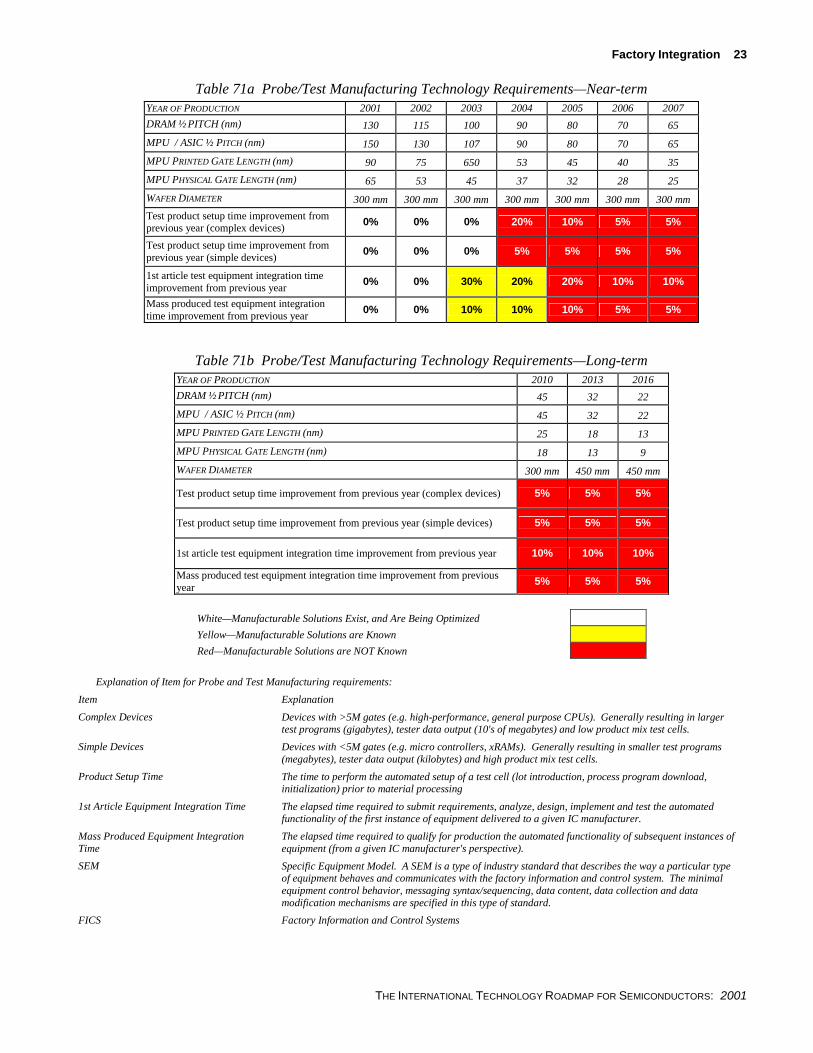
Factory Integration 23
THE INTERNATIONAL TECHNOLOGY ROADMAP FOR SEMICONDUCTORS: 2001
Table 71a Probe/Test Manufacturing Technology Requirements—Near-term YEAR OF PRODUCTION 2001 2002 2003 2004 2005 2006 2007 DRAM ½ PITCH (nm) 130 115 100 90 80 70 65 MPU / ASIC ½ PITCH (nm) 150 130 107 90 80 70 65 MPU PRINTED GATE LENGTH (nm) 90 75 650 53 45 40 35 MPU PHYSICAL GATE LENGTH (nm) 65 53 45 37 32 28 25 WAFER DIAMETER 300 mm 300 mm 300 mm 300 mm 300 mm 300 mm 300 mm Test product setup time improvement from previous year (complex devices) 0% 0% 0% 20% 10% 5% 5%
Test product setup time improvement from previous year (simple devices) 0% 0% 0% 5% 5% 5% 5%
1st article test equipment integration time improvement from previous year 0% 0% 30% 20% 20% 10% 10%
Mass produced test equipment integration time improvement from previous year 0% 0% 10% 10% 10% 5% 5%
Table 71b Probe/Test Manufacturing Technology Requirements—Long-term YEAR OF PRODUCTION 2010 2013 2016 DRAM ½ PITCH (nm) 45 32 22 MPU / ASIC ½ PITCH (nm) 45 32 22 MPU PRINTED GATE LENGTH (nm) 25 18 13 MPU PHYSICAL GATE LENGTH (nm) 18 13 9 WAFER DIAMETER 300 mm 450 mm 450 mm
Test product setup time improvement from previous year (complex devices) 5% 5% 5%
Test product setup time improvement from previous year (simple devices) 5% 5% 5%
1st article test equipment integration time improvement from previous year 10% 10% 10%
Mass produced test equipment integration time improvement from previous year 5% 5% 5%
White—Manufacturable Solutions Exist, and Are Being Optimized
Yellow—Manufacturable Solutions are Known
Red—Manufacturable Solutions are NOT Known
Explanation of Item for Probe and Test Manufacturing requirements: Item Explanation Complex Devices Devices with >5M gates (e.g. high-performance, general purpose CPUs). Generally resulting in larger
test programs (gigabytes), tester data output (10's of megabytes) and low product mix test cells. Simple Devices Devices with <5M gates (e.g. micro controllers, xRAMs). Generally resulting in smaller test programs
(megabytes), tester data output (kilobytes) and high product mix test cells. Product Setup Time The time to perform the automated setup of a test cell (lot introduction, process program download,
initialization) prior to material processing 1st Article Equipment Integration Time The elapsed time required to submit requirements, analyze, design, implement and test the automated
functionality of the first instance of equipment delivered to a given IC manufacturer. Mass Produced Equipment Integration Time
The elapsed time required to qualify for production the automated functionality of subsequent instances of equipment (from a given IC manufacturer's perspective).
SEM Specific Equipment Model. A SEM is a type of industry standard that describes the way a particular type of equipment behaves and communicates with the factory information and control system. The minimal equipment control behavior, messaging syntax/sequencing, data content, data collection and data modification mechanisms are specified in this type of standard.
FICS Factory Information and Control Systems

24 Factory Integration
THE INTERNATIONAL TECHNOLOGY ROADMAP FOR SEMICONDUCTORS: 2001
POTENTIAL SOLUTIONS The principal goals of factory integration are maintaining cost per unit area of silicon, decreasing factory ramp time, and increasing factory flexibility to changing technology and business needs. The three difficult challenges of complexity management, factory optimization, and extendibility, flexibility and scalability must be addressed to achieve these goals. Potential solutions are identified for Factory Operations, Production Equipment, Material Handling Systems, Factory Information and Control Systems, Facilities, and Probe/Test Manufacturing. Note that the bars containing wafer diameter data represent potential solutions that are wafer-size specific.
Potential solutions are shown as Research required, Development underway, and Qualification/ pre-production. The purpose is to provide guidance to researchers, suppliers and IC makers on the timing required to successfully implementing solutions into factories. For simplicity, these activities are serial in each table; however, they overlap each other in practice.
FACTORY OPERATIONS
Figure 45 Factory Operations Potential Solutions
2003 2005 20072001 2011 2013 20152009 2017
Research Required Development Underway Qualification/Pre-Production
This legend indicates the time during which research, development, and qualification/pre-production should be taking place for the solution.
First Year of IC Production2004 2006 20082002 2012 2014 20162010
DECISION SUPPORT TOOLS FOROPERATIONAL IMPROVEMENT
Tools for understanding components of cycle time and trade-off between cycle time and equipment utilization and hot lotsTools/algorithms/models for wafer release (start) policies based on bottleneck monitoringTools/algorithms/models for forecasting demand and capacity-demand integrationTools to accurately predict and analyze individual lot cycle times to ensure On-Time-Delivery (OTD)Tools/algorithms/models for optimized operator and technician staffing levels and developing optimal training/cross-training plansIntegrated techniques for coordination with supply chain management efforts (fab/sort/assy/test/distribution)Tools for determining optimum quantities and timings of operations resources (such as Reticle and Spares quantities)Tools for determining optimal Non-product wafer plansTools/algorithms/models to measure actual capacity loss components due to operators and technicians
EXECUTION TOOLS FOROPERATIONAL IMPROVEMENT
Real-time scheduling and dispatching algorithms integrated with AMHS - must consider operations resources, labor, Non product wafer, status of equipment (PM) and factoryPlanning systems integrated with real-time scheduling and dispatching systemsReal-time optimization of operator and technician activitiesSpares usage optimization and tracking and control capabilityReal-time factory supply chain management & real-time control capability
300 mm 450 mm
300 mm 450 mm
300 mm 450 mm
300 mm 450 mm
300 mm Applies for 450 mm
300 mm 450 mm
300 mm 450 mm
300 mm 450 mm
300 mm 450 mm
300 mm 450 mm
300 mm 450 mm
300 mm 450 mm
300 mm Applies for 450 mm
300 mm 450 mm
2003 2005 20072001 2011 2013 20152009 20172003 2005 20072001 2011 2013 20152009 2017
Research Required Development Underway Qualification/Pre-Production
This legend indicates the time during which research, development, and qualification/pre-production should be taking place for the solution.
First Year of IC Production2004 2006 20082002 2012 2014 201620102004 2006 20082002 2012 2014 20162010
DECISION SUPPORT TOOLS FOROPERATIONAL IMPROVEMENT
Tools for understanding components of cycle time and trade-off between cycle time and equipment utilization and hot lotsTools/algorithms/models for wafer release (start) policies based on bottleneck monitoringTools/algorithms/models for forecasting demand and capacity-demand integrationTools to accurately predict and analyze individual lot cycle times to ensure On-Time-Delivery (OTD)Tools/algorithms/models for optimized operator and technician staffing levels and developing optimal training/cross-training plansIntegrated techniques for coordination with supply chain management efforts (fab/sort/assy/test/distribution)Tools for determining optimum quantities and timings of operations resources (such as Reticle and Spares quantities)Tools for determining optimal Non-product wafer plansTools/algorithms/models to measure actual capacity loss components due to operators and technicians
EXECUTION TOOLS FOROPERATIONAL IMPROVEMENT
Real-time scheduling and dispatching algorithms integrated with AMHS - must consider operations resources, labor, Non product wafer, status of equipment (PM) and factoryPlanning systems integrated with real-time scheduling and dispatching systemsReal-time optimization of operator and technician activitiesSpares usage optimization and tracking and control capabilityReal-time factory supply chain management & real-time control capability
300 mm300 mm 450 mm450 mm
300 mm300 mm 450 mm450 mm
300 mm 450 mm300 mm300 mm 450 mm450 mm
300 mm 450 mm300 mm300 mm 450 mm450 mm
300 mm Applies for 450 mm300 mm300 mm Applies for 450 mmApplies for 450 mm
300 mm 450 mm300 mm300 mm 450 mm450 mm
300 mm 450 mm300 mm300 mm 450 mm450 mm
300 mm 450 mm300 mm300 mm 450 mm450 mm
300 mm 450 mm300 mm300 mm 450 mm450 mm
300 mm 450 mm300 mm300 mm 450 mm450 mm
300 mm 450 mm300 mm300 mm 450 mm450 mm
300 mm 450 mm300 mm300 mm 450 mm450 mm
300 mm Applies for 450 mm300 mm300 mm Applies for 450 mmApplies for 450 mm
300 mm 450 mm300 mm300 mm 450 mm450 mm

Factory Integration 25
THE INTERNATIONAL TECHNOLOGY ROADMAP FOR SEMICONDUCTORS: 2001
PRODUCTION EQUIPMENT
Figure 46 Production Equipment Potential Solutions
2003 2005 20072001 2011 2013 20152009 2017
Research Required Development Underway Qualification/Pre-Production
This legend indicates the time during which research, development, and qualification/pre-production should be taking place for the solution.
First Year of IC Production2004 2006 20082002 2012 2014 20162010
Cost Reduction by Standards & InteroperabilityStandard interfaces for wafer and carrier handling, communications interfaces, material handling, facilities systems (utilities, drains and exhaust), operations and equipment maintenance.Equipment manuals, schematics, drawings, and specifications accessible and browseable using mainstream Internet technology, internet standards, and user-interfaces.
OEE ImprovementProliferation of in-situ monitoring and recipe adjustable parameters.Statistical analysis and feedback control improvements, enable all logs & parameter related data to leave tool in an orderly manner; permit controlled remote interruption of processes at a step/recipe level; allow remote systems to take chambers in the middle of lot processing without impacting other chamber’s process.Smarter embedded tool controller, precise wafer handling & particulate control, eliminate dwell-time between wafer handling moves and increase processing wafer/hour rate.Self-diagnostic & remote diagnostic supported by fault detection/classification, run to run control and integrated metrologySingle-wafer level tracking and control.
More Efficient Equipment DesignsRecycle/re-use more waterSeparate waste streams at the toolHeat load removal from tool by usage of process cooling water versus HVAC systems
High efficiency power distributions systems in the tool (usehigher voltage, not current)
Spares Cost ReductionIncreased modularization, permit change out and remote service to minimize downtime, optimized PM frequency, consumables modular system components
Ramp-up Cycle-time ReductionQualification period reduction (more pre-qualification at supplier site)
Installation period reduction (quicker assembly on-site)
Multiple-Generation (node) UpgradabilityHigh exchangeability of chamber modules, parts and fittings
Common equipment base, frame and modules, Modular equipment control systems
Carrier level and Wafer level integrated Flow and ControlsType1: Sorter and Metrology integrated with StockersType 2-1: Connected EFEM type equipmentType 2-2: Expanded EFEM type equipment
Type 2-3: Continuous EFEM type equipment
300mm
300mm 450mm
300mm 450mm
300mm 450mm
300mm 450mm
300mm 450mm
300mm 300mm 450mm
300mm 300mm 450mm
300mm 300mm 450mm
300mm 450mm
300mm 450mm
300mm 450mm
300mm 450mm
300mm 450mm
300mm 450mm
300mm 450mm
300mm 450mm
300mm 450mm
300mm 450mm
300mm 450mm
2003 2005 20072001 2011 2013 20152009 20172003 2005 20072001 2011 2013 20152009 2017
Research Required Development Underway Qualification/Pre-Production
This legend indicates the time during which research, development, and qualification/pre-production should be taking place for the solution.
First Year of IC Production2004 2006 20082002 2012 2014 201620102004 2006 20082002 2012 2014 20162010
Cost Reduction by Standards & InteroperabilityStandard interfaces for wafer and carrier handling, communications interfaces, material handling, facilities systems (utilities, drains and exhaust), operations and equipment maintenance.Equipment manuals, schematics, drawings, and specifications accessible and browseable using mainstream Internet technology, internet standards, and user-interfaces.
OEE ImprovementProliferation of in-situ monitoring and recipe adjustable parameters.Statistical analysis and feedback control improvements, enable all logs & parameter related data to leave tool in an orderly manner; permit controlled remote interruption of processes at a step/recipe level; allow remote systems to take chambers in the middle of lot processing without impacting other chamber’s process.Smarter embedded tool controller, precise wafer handling & particulate control, eliminate dwell-time between wafer handling moves and increase processing wafer/hour rate.Self-diagnostic & remote diagnostic supported by fault detection/classification, run to run control and integrated metrologySingle-wafer level tracking and control.
More Efficient Equipment DesignsRecycle/re-use more waterSeparate waste streams at the toolHeat load removal from tool by usage of process cooling water versus HVAC systems
High efficiency power distributions systems in the tool (usehigher voltage, not current)
Spares Cost ReductionIncreased modularization, permit change out and remote service to minimize downtime, optimized PM frequency, consumables modular system components
Ramp-up Cycle-time ReductionQualification period reduction (more pre-qualification at supplier site)
Installation period reduction (quicker assembly on-site)
Multiple-Generation (node) UpgradabilityHigh exchangeability of chamber modules, parts and fittings
Common equipment base, frame and modules, Modular equipment control systems
Carrier level and Wafer level integrated Flow and ControlsType1: Sorter and Metrology integrated with StockersType 2-1: Connected EFEM type equipmentType 2-2: Expanded EFEM type equipment
Type 2-3: Continuous EFEM type equipment
300mm 300mm
300mm 450mm 300mm 450mm
300mm 450mm 300mm 450mm
300mm 450mm 300mm 450mm
300mm 450mm 300mm 450mm
300mm 450mm 300mm 450mm
300mm 300mm 450mm 300mm 300mm 450mm
300mm 300mm 450mm 300mm 300mm 450mm
300mm 300mm 450mm 300mm 300mm 450mm
300mm 450mm 450mm
300mm 450mm 300mm 450mm
300mm 450mm 300mm 450mm
300mm 450mm 300mm 450mm
300mm 450mm 300mm 450mm
300mm 450mm 300mm 450mm
300mm 450mm 300mm 450mm
300mm 450mm 300mm 450mm
300mm 450mm 300mm 450mm
300mm 450mm 300mm 450mm
300mm 450mm 300mm 450mm

26 Factory Integration
THE INTERNATIONAL TECHNOLOGY ROADMAP FOR SEMICONDUCTORS: 2001
MATERIAL HANDLING SYSTEMS
[1] For software integration solutions, see Factory Information and Control Systems
Figure 47 Material Handling Systems Potential Solutions
2003 2005 20072001 2011 2013 20152009 20172003 2005 20072001 2011 2013 20152009 2017
Research Required Development Underway Qualification/Pre-Production
This legend indicates the time during which research, development, and qualification/pre-production should be taking place for the solution.
First Year of IC Production2004 2006 20082002 2012 2014 201620102004 2006 20082002 2012 2014 20162010
EASE OF IMPLEMENTATION/QUICK RAMPUP / MAINTENANCE
Simple system component modules with automated or zero field hardware alignment and positioning capability (cleanroom support structure, teaching, and adjustment not required) Easily extended transport system rail
Automated software configuration (HW independent structure and parameter setting)Dynamic (high volume transfer load) simulation test and automatic transfer capability estimation (throughput and carrierdelivery time)Automated preventive/predictive maintenance, calibration, fine tuning, software upgrade (uninterrupted) and e-Diagnostics
MATERIAL TRANSPORTSYSTEM CONFIGURATIONS
High throughput vehicle based direct transport system with by-pass capability Large scale, high throughput conveyors and next generation vehicles
MATERIAL HANDLING STORAGESYSTEM CONFIGURATIONS
Central storage systems for low use non-production lots using zero fab floor space. Conveyor based storage system for using zero fab floor space.Modular field upgradeable stockers which are expandable to very large capacity
TRANSPORT LOADIDENTIFICATION & TRACKINGMETHODS
Carrier identification system for separate tracking of empty carrier and lidWafer ID reading to support 450mm wafer tracking
MATERIAL HANDLING CONTROLCAPABILITY
Integrated material control system for interbay and intrabay controlIntelligent vehicle traffic management control for direct transport system and advanced reticle transportation integration Flexible lot size transport, capable of handling split and merge. (Note: same size carrier with variety of multiple lots)
450 mm
300 mm300 mm
300 mm
300 mm
300 mm
300 mm
300 mm
300 mm
450 mm300 mm300 mm
300 mm
300 mm
450 mm
300 mm300 mm
450 mm
300 mm300 mm

Factory Integration 27
Research R equired Development Underway Qualification/Pre-Production
This legend indicates the ti me during which research, development, and qualification/pre-pr oduction shoul d be taking place for the sol ution.
INTEGRATED FLOW AND CONTROLSYSTEMS (continued)Wafer Level (Extended EFEMs)
Extended EFEMs with high-speed waf er transf er robot and standard equipment hardware and sof tware interf aces f or easy equipment and load port add-onsIntegrated operational model; using equipment throughput matching algorithms and including robust waf er dispatcher and exception handling
Wafer Level (Continuous EFEMs)Ultra high speed waf er transport sy stem and stockers with high speed waf er sorting capability (lot to waf er transition between stocker and transport) and standard interf acesSystem lev el controller with waf er lev el dispatcher
450 mm INTERFACE STANDARDSDEVELOPMENT
Interf ace standards dev elopment f or storage, transport, carriers, and equipment
450 mm
300 mm
450 mm
2004 20072001 2013 20162010First Year of IC Production
300 mm
450 mm
Research R equired Development Underway Qualification/Pre-Production
This legend indicates the ti me during which research, development, and qualification/pre-pr oduction shoul d be taking place for the sol ution.
Research R equired Development Underway Qualification/Pre-Production
This legend indicates the ti me during which research, development, and qualification/pre-pr oduction shoul d be taking place for the sol ution.
INTEGRATED FLOW AND CONTROLSYSTEMS (continued)Wafer Level (Extended EFEMs)
Extended EFEMs with high-speed waf er transf er robot and standard equipment hardware and sof tware interf aces f or easy equipment and load port add-onsIntegrated operational model; using equipment throughput matching algorithms and including robust waf er dispatcher and exception handling
Wafer Level (Continuous EFEMs)Ultra high speed waf er transport sy stem and stockers with high speed waf er sorting capability (lot to waf er transition between stocker and transport) and standard interf acesSystem lev el controller with waf er lev el dispatcher
450 mm INTERFACE STANDARDSDEVELOPMENT
Interf ace standards dev elopment f or storage, transport, carriers, and equipment
450 mm450 mm
300 mm300 mm
450 mm450 mm
2004 20072001 2013 20162010First Year of IC Production 2004 20072001 2013 20162010First Year of IC Production
300 mm300 mm
450 mm450 mm
[1] For software integration solutions, see Factory Information and Control Systems Section
THE INTERNATIONAL TECHNOLOGY ROADMAP FOR SEMICONDUCTORS: 2001
Figure 47 Material Handling Systems Potential Solutions (continued)

28 Factory Integration
THE INTERNATIONAL TECHNOLOGY ROADMAP FOR SEMICONDUCTORS: 2001
FACTORY INFORMATION AND CONTROL SYSTEMS
Figure 48 Factory Information and Control Systems (FICS) Potential Solutions
2003 2005 20072001 2011 2013 20152009 20172003 2005 20072001 2011 2013 20152009 2017
Research Required Development Underway Qualification/Pre-Production
This legend indicates the time during which research, development, and qualification/pre-production should be taking place for the solution.* Includes development of Standards and Standards-Based Solutions
Research Required Development Underway Qualification/Pre-Production
This legend indicates the time during which research, development, and qualification/pre-production should be taking place for the solution.* Includes development of Standards and Standards-Based Solutions
First Year of IC Production2004 2006 20082002 2012 2014 201620102004 2006 20082002 2012 2014 20162010
Improve Factory EffectivenessCycle Time and Throughput
Real-time dispatching and direct transport with integration of Dispatcher, MES, AMHS, equipment availability and yield dataFICS that support multiple recipes/lots per carrierE-Diagnostics to support automated preventative/predictive maintenance, calibration, fine tuning, software upgrades for production and AMHS equipment
Highly Reliable SystemsFault tolerant computer systems with transparent hardware switching for failures (minimal to no impact)Software application fault detection & monitoring
Low Maintenance SystemsSoftware applications capable of dynamic upgrades (minimal to no impact)Databases capable of dynamic upgrades (minimal to no impact)Automatic/Dynamic AMHS software (MCS) reconfigurationIntegration testing and volume testing of overall factory systems (incl AMHS) through simulators or emulators
Flexible Manufacturing SystemsScalable system performanceWeb capable interfaces for factory systemsWireless/portable user interfaces
IMPROVE FACTORY YIELDRecipe management for all assembly production equipmentEquipment Engineering Fault Detection and Control (FDC)
Standardized historical and summary data storage/analysis*Standardized detailed wafer and chamber data tracking*Standardized configurable/downloadable FDC models*Standardized FDC signals from equipment to host*Standardized Host-issued FDC control commands*
Equipment Engineering (EE) Run-to-Run Control Standardized Modular Applications with Open Interfaces*Standardized MES recipe interaction*Standardized Recipe Adjustment (process/control job)*Standardized Metrology data collection via EE interface*Standardized Wafer-level and Chamber-level data collection via EE interface*
Equipment Engineering (EE) Integrated MetrologyStandardized Metrology/process data collection via EE interface*Standardized GEM interface for integrated process/metrology control*Standardized Recipe and Model selection/download for integrated process/metrology*
Real-time yield management systems to correlate test/probe and process data to automatically determine process problems
ACCOMMODATE PROCESS AND PRODUCT COMPLEXITY
Integrated FICS to facilitate data searches and information correlation on process and operational dataIntegrated MCS for interbay/intrabay controlIntegrated FICS to support cross-site processingBusiness-level software systems integrated with FICS
FACTORY SYSTEMS (FS) REUSEReplace SECS/GEM with mainstream-based standardsCollaboration/Prototyping to decrease Standards cycle time
INCREASING PURITY REQUIREMENTS FOR PROCESS AND MATERIALImprove systems to monitor and control chemical, safety and environmental items
300mm
300mm 300mm300mm
300mm 300mm 300mm
300mm300mm
450mm 450mm 300mm
300mm300mm
300mm300mm
300mm300mm
300mm 300mm
300mm 300mm
300mm300mm
300mm 300mm
300mm 300mm
300mm 300mm
300mm 300mm
300mm 300mm
300mm300mm
300mm 300mm
300mm
300mm 300mm
300mm 300mm 300mm
300mm300mm
300mm300mm
300mm300mm
300mm300mm
300mm300mm
300mm300mm
300mm300mm
300mm300mm
300mm300mm
300mm300mm
300mm 300mm 300mm
300mm 300mm 300mm
300mm 300mm 300mm
450mm 450mm
450mm 450mm

Factory Integration 29
THE INTERNATIONAL TECHNOLOGY ROADMAP FOR SEMICONDUCTORS: 2001
FACILITIES
Figure 49 Facilities Potential Solutions
2003 2005 20072001 2011 2013 2015 2009 2017
Research Required Development Underway Qualification/Pre - Production This legend indicates the time during which research, developmen t, and qualification/pre -production should be taking place for the solution.
First Year of IC Production 2004 2006 20082002 2012 2014 20162010
Facility Cost Reduction Use benchmarking to develop standard performance metrics and best practices for facility construction, operation, reliabi lity and equipment installation Develop Standard facility designs and specifications that reduce unique custom factory designs allowing earlier design packages for construction Develop more robust design tools Provide better quality utility requirements for production equipment Design tools for clean maintenance to ensure isolation is maintained during routine maintenance operationsDevelop Power and water reduction protocols in conjunction with production equipment manufacturers Reduce move - in size of production equipment to minimize aisle widths Improve factory layout density/ vertical layout optimizationStandardize measuring and reporting of utility utilization at production equipment
Efficient Production Equipment InstallationDevelop More Accurate Factory Models Develop Flexible Factory Designs that allow installation, removal, and reconfiguration of production equipment over the life of the factory Develop Production Equipment Installation Standards using Predictable/Consistent tool connection for utilities, drains, exhaust and interconnects Ensure early and accurate identification of production equipment installation demand requirements ( eg. pressure, loads, flows, connection size) Design Production Equipment to operate within facility infrastructure systems capabilities Design support equipment to fit production equipment footprint determined by prime manufacturing area Improve production equipment documentation and change management Reduce makeup air & exhaust requirements
Facility Solutions for ESH RequirementsTransition to higher efficiency (voltage) power distributionMaintain or reduce radiation exposure in the facility (EUV Impact) Recycle/Retreat water and waste streams Investigate ROI and incentives for alternative power solutionsTransition from air to more efficient liquid cooling systems in cooperation with production equipment manufacturesDevelop Risk Assessment tools for understanding economic impact to EHS design and measurement incentivesProvide cost effective point of use and/or factory wide abatement technologies
300mm
300mm
300mm
300mm
300mm
300mm
300mm
300mm
300mm
300mm
300mm
300mm
300mm
300mm
300mm
300mm
300mm
300mm
300mm 450mm
450mm 450mm
450mm
450mm
450mm
450mm
450mm
450mm
450mm
300mm
300mm
300mm
300mm
300mm
450mm 450mm
450mm
450mm
2003 2005 20072001 2011 2013 2015 2009 20172003 2005 20072001 2011 2013 2015 2009 2017
Research Required Development Underway Qualification/Pre - Production This legend indicates the time during which research, developmen t, and qualification/pre -production should be taking place for the solution.
First Year of IC Production 2004 2006 20082002 2012 2014 20162010 2004 2006 20082002 2012 2014 20162010
Facility Cost Reduction Use benchmarking to develop standard performance metrics and best practices for facility construction, operation, reliabi lity and equipment installation Develop Standard facility designs and specifications that reduce unique custom factory designs allowing earlier design packages for construction Develop more robust design tools Provide better quality utility requirements for production equipment Design tools for clean maintenance to ensure isolation is maintained during routine maintenance operationsDevelop Power and water reduction protocols in conjunction with production equipment manufacturers Reduce move - in size of production equipment to minimize aisle widths Improve factory layout density/ vertical layout optimizationStandardize measuring and reporting of utility utilization at production equipment
Efficient Production Equipment InstallationDevelop More Accurate Factory Models Develop Flexible Factory Designs that allow installation, removal, and reconfiguration of production equipment over the life of the factory Develop Production Equipment Installation Standards using Predictable/Consistent tool connection for utilities, drains, exhaust and interconnects Ensure early and accurate identification of production equipment installation demand requirements ( eg. pressure, loads, flows, connection size) Design Production Equipment to operate within facility infrastructure systems capabilities Design support equipment to fit production equipment footprint determined by prime manufacturing area Improve production equipment documentation and change management Reduce makeup air & exhaust requirements
Facility Solutions for ESH RequirementsTransition to higher efficiency (voltage) power distributionMaintain or reduce radiation exposure in the facility (EUV Impact) Recycle/Retreat water and waste streams Investigate ROI and incentives for alternative power solutionsTransition from air to more efficient liquid cooling systems in cooperation with production equipment manufacturersDevelop Risk Assessment tools for understanding economic impact to EHS design and measurement incentivesProvide cost effective point of use and/or factory wide abatement technologies
300mm
300mm
300mm
300mm
300mm
300mm
300mm
300mm
300mm
300mm
300mm
300mm
300mm
300mm
300mm
300mm
300mm
300mm
300mm 450mm
450mm 450mm
450mm
450mm
450mm
450mm
450mm
450mm
450mm
300mm
300mm
300mm
300mm
300mm
450mm 450mm
450mm
450mm

30 Factory Integration
THE INTERNATIONAL TECHNOLOGY ROADMAP FOR SEMICONDUCTORS: 2001
PROBE/TEST MANUFACTURING
Figure 50 Probe/Test Manufacturing Potential Solutions
CROSSCUT ISSUES
ENVIRONMENTAL, SAFETY AND HEALTH ESH continues to play a very important role in factory design and operation. Decisions made at the earliest stages of factory planning will have a dramatic impact on the ability of that factory to economically meet rigorous safety and environmental requirements. Early consideration of safe and environmentally responsible design is essential to develop factories that comply with ESH requirements while achieving rapid start-up schedules and avoiding costly redesigns and retrofits.
New facilities designs and retrofits of existing ones are much more impacted by such changes as 200 mm to 300 mm conversion, introduction of factory-wide mini-environment based equipment, copper processing, and reticle purging requirements when compared to facilities changes needed when moving from one technology node to the next. Equipment suppliers have made good progress integrating point of use abatement devices and the tool. However, tool footprint in the sub-fab has increased significantly as a result. An immediate challenge therefore is to find an efficient tool design that incorporates point of use devices without an overall increase in footprint both in the fab as well as in the sub-fab.
A plan for continuous improvement of safety in future factories must be established. A thorough understanding of safety risks associated with automated equipment will lead to standards that assure safe working conditions for both people and product. These standards must be directed at the integrity of automated systems, the tools with which they interface, and the interfaces as well.
Our industry faces increasing environmental limitations. The availability of adequate water supply already places restrictions on the size and location of factories. The goal is to build factories that minimize resource consumption and maximize resource reclamation. Effluents of environmentally toxic materials need to be reduced to near zero—perhaps to zero levels.
Conservation of energy is very critical, more than ever before. The constraint to this is the size of the factory, which then puts a very large potential pollution burden on the energy provider and the wafer fabrication plant.
While much of the responsibility for ESH programs rests with the equipment suppliers, application of advanced resource management programs will have a significant impact. International ESH standardization and design programs can be greatly enhanced through training programs established for and by the industry. Consideration of ESH standards in
2003 2005 20072001 2011 2013 20152009 2017
Research Required Development Underway Qualification/Pre-Production
This legend indicates the time during which research, development, and qualification/pre-production should be taking place for the solution.
First Year of IC Production2004 2006 20082002 2012 2014 20162010
Standards Based Equipment and FICSTest equipment and FICS solutions with standardized software control interfaces (Revised SEM)Prober equipment and FICS solutions with standardized software control interfaces (Revised SEM)Handler equipment and FICS solutions with standardized software control interfaces (Revised SEM)Test equipment and FICS solutions with standardized result dataTest equipment and FICS solutions with standardized test program formats and interfaces
300mm
300mm
300mm
300mm
300mm
450mm
450mm
450mm
450mm
450mm
2003 2005 20072001 2011 2013 20152009 20172003 2005 20072001 2011 2013 20152009 2017
Research Required Development Underway Qualification/Pre-Production
This legend indicates the time during which research, development, and qualification/pre-production should be taking place for the solution.
First Year of IC Production2004 2006 20082002 2012 2014 201620102004 2006 20082002 2012 2014 20162010
Standards Based Equipment and FICSTest equipment and FICS solutions with standardized software control interfaces (Revised SEM)Prober equipment and FICS solutions with standardized software control interfaces (Revised SEM)Handler equipment and FICS solutions with standardized software control interfaces (Revised SEM)Test equipment and FICS solutions with standardized result dataTest equipment and FICS solutions with standardized test program formats and interfaces
300mm
300mm
300mm 300mm
300mm 300mm
300mm 300mm
450mm
450mm
450mm
450mm
450mm

Factory Integration 31
THE INTERNATIONAL TECHNOLOGY ROADMAP FOR SEMICONDUCTORS: 2001
equipment design, maintenance, de-commissioning and final disposition will reap substantial rewards in ESH performance as well as cost.
ASSEMBLY AND PACKAGING Process flow complexity and the proliferation of form factors in recent years have resulted in increased use of materials handling and software automation in the assembly and packaging phase of semiconductor manufacturing, leading to higher costs and flexibility challenges.
Material handling costs are driven by indirect materials such as carts, magazines, carriers, and trays, which are used to transport product between tools and transfer product within tools. Other material handling costs result from capital equipment used to load and/or transfer product.
Equipment automation software costs are driven by the lack of relevant standards, and/or the lack of adherence to existing standards. This requires the development of custom software interface. Demand in this software automation in the assembly and packaging areas has increased dramatically as the desire to trace units throughout their production cycle are coupled with the desire to have the data and control that increases capital equipment productivity.
To meet industry trends of declining average selling prices and increased market segmentation, significant cost reductions and flexibility improvements are needed in the areas of material handling and equipment communications. Applying the roadmap process to identify requirements and implement standards for carriers, media and hardware/software equipment interfaces in assembly and packaging manufacturing are potential solutions to these cost issues. (Refer to supplemental files for additional backup material on assembly and packaging.)
Table 72 Assembly and Packaging Potential Solutions KEY ISSUES POTENTIAL SOLUTIONS Material Handling Costs Carrier and Media standards
Production equipment load/unload interface standards
Equipment Communication Costs Adherence to existing proven standards Standard behavioral Models across equipment types Use of mainstream computing standards for equipment to host communication to
reduce cost and complexity
YIELD MANAGEMENT Development of good yield management strategies reduces costs and investment risks. A factory yield model defines typical operational performance and permits a Pareto of performance and yield detractors. A factory model based on experimental mapping of process parameters and process control strategies reduces the need for increased metrology tools and monitor wafers. It is also critical to determine tolerance variations for process parameters and interactions between processes to reduce reliance on end-of-line inspections. Factory models should also be capable of handling defect reduction inputs to assure efficient factory designs for rapid construction, rapid yield ramp, high equipment utilization, and extendibility to future technology nodes. Table 73 outlines defect reduction needs.
Yield Management systems (YMS) must be developed that can access and correlate information from multiple data sources. YMS should also work with measurement/metrology equipment from multiple suppliers using pre-competitive standards based data formats.

32 Factory Integration
THE INTERNATIONAL TECHNOLOGY ROADMAP FOR SEMICONDUCTORS: 2001
Table 73 Yield Management Potential Solutions Key Issues Potential Solutions Tolerance Variations for Critical Process Parameters Process control enablers and extendibility Root cause analysis of performance detractors
Experimental mapping of the parameter space for each process and correlation to device performance
Process Interactions Wafer state analysis Initial equipment state consistency Impact of contamination on OEE
Short loop modeling and experimental mapping of parameter state variations Component wear and lifetime studies
Process Critical Fluids and Materials Purity Requirements Point of Use contamination monitoring Materials reliability and consistency
Industry test structure for each node on roadmap Process parameter studies
Reduce End Of Line Inspection And Monitor Wafers Non-visual defect detection Metrology for <.08 µm defects
In situ process control
Yield Management System Flexibility Interoperability of equipment and data sources with YMS Standards for equipment data formats Rapid Yield Ramp Process specific yield models Process control
Inline inspection metrology Correlation of parameter space variation and defects
Facilities Impact to Yield Electromagnetic interference Vibration Molecular contamination
Short loop models Data/metrics standards
METROLOGY INTEGRATION Metrology systems must be fully integrated into the factory information and control systems to facilitate run-to-run process control, yield analysis, material tracking through manufacturing, and other off-line analyses. The scope of measurement data sources will extend from key suppliers (masks and silicon wafers) through fab, probe, assembly, final test and be linked to business enterprise level information. This data-to-information capability should exist as early as possible in a factory’s history to minimize the time spent qualifying equipment and ramping the factory to production. Data volumes and data rates will continue to increase dramatically due to wafer size increases and process technology shrinks. Analysis of this data will require connectivity and correlation to multiple data sources across the factory (fab, probe, etc.). In 300 mm factories, review and classification tools may eventually appear in clusters or integrated clusters to create a more efficient factory interface. Some 300 mm process equipment will include integrated measurement (IM) capabilities to reduce cycle time and wafer-to-wafer process variance. Integrated metrology must be fully integrated to the process equipment embedded control system and not add to the process equipment footprint, and be selected carefully by IC makers to balance. IM costs must be carefully balanced against benefits to make specific implementation decisions that improve the overall factory productivity.
STATIC CHARGE CONTROL Electrostatic charge adversely impacts every phase of semiconductor manufacturing, causing three basic problems. Electrostatic attracted (ESA) contamination increases as particle size decreases, making defect density targets more difficult to attain. Electrostatic discharge (ESD) causes damage to devices and photomasks. Shrinking device feature size means less energy is required in an ESD event to cause device or mask damage. Low humidity in 157 nm lithography results in higher charge levels increasing ESD risks to masks. Equipment malfunctions due to ESD-related electromagnetic interference (EMI) reduce OEE, and have become more frequent as equipment microprocessor operating speeds increase. These problems occur where bare wafers and reticles are produced, where devices are produced in wafer fabs, and where individual devices are produced in backend packaging, assembly, and test. (Link to supplemental material for additional details on ESD technology requirements and potential solutions.)

Factory Integration 33
THE INTERNATIONAL TECHNOLOGY ROADMAP FOR SEMICONDUCTORS: 2001
FACTORY INTERFACE STANDARDS REQUIREMENTS Standards work best when applied to pre-competitive areas, and when there is a benefit to all participants. Successful development, implementation, and testing of non-proprietary standards have major ramifications on the factory ability to rapidly come online and ramp to full volume in a cost-effective manner. Standardization of inter-operating elements, especially interfaces between different systems in a factory, improves the industry’s ability to manage rising factory complexity.
Global cooperation among IC manufacturers and equipment suppliers for 300 mm factories has resulted in the definition and implementation of many non-proprietary factory integration standards. This has provided enormous industry benefits by minimizing equipment development time, reducing the cost and risk of development, and has helped reduce factory complexity.
Figure 51 shows industry progress toward the development and implementation of 300 mm standards. It also identifies areas of future work where standards do not exist, but are needed. This is shown with respect to four critical areas of the factory, which have maximum benefits from global cooperation—production equipment, facility systems, material handling systems, and factory information and control systems. Refer to the supplemental file link for additional details on industry standards.)
Figure 51 Integrated Factory Interface Standards
Utility, fluids,exhaust, drains hook-upstandards
Factory Information andControl Systems
Production EquipmentIntegratedmini-environmentstandards
Rear user-interfacestandards
PGV dockingstandards
Loadportstandards
Wafer & carrierstandards
Carrier IDstandards
Buffering standardsfor continuousoperation
Standards forsafety counter-measures
Carrierenvironmentstandards
Equipment footprint& height managementstandards
Reticle carrier &loadport standards
ProductionEquipment(side view)
Enhanced parallelI/O standard for groundbased transporters
Enhanced parallel I/O standard for ceiling basedtransporters
FactoryNetwork
SECS-IIGEMHSMS
Utilization trackingstandard
Enhanced parallelI/O standards
Carrier mgtstandard
Process Job,Control Jobstandards
Wafer level tracking &control standards
CarrierID standard
Mainstream Computer Communications stds
ManufacturingExecutionSystems
DecisionSupportSystems
Productionequipment
ProcessControlstandards
User Interfaces
OtherSystems
Standard for dataformats, data access, and inter applicationinterfaces
Facilities Systems
Rear of productionequipment
Fab levels
Maximummove-in size stds
Sub-fab standards
Raised floorheight standards
Wall interfacestandards
RearU/I
Maxweightstandard
Standards for facilities systems safety counter-measures
Materials supplycontainer standards
Standards for installpedestals, jigs/fixturefor alignment
Work accessstandards to eliminateErgo issues
Cleanroom NoiseCriteria standards
Vibration stds
Global ConstructionCodes
Isolation standards forequipment maintenance
Material Handling Systems
Sub-fab level
Bay ceiling
Stoc
ker
Tall
Stoc
ker
Stoc
ker
Standards for integrated transport systems that perform both interbayand intrabay transport functions
Stocker to transporterinterface standards
Transporter to loadportinterface standards
Standards for safetycounter-measures
TransportSEM
StockerSEM
Dee
p St
ocke
r
Fab level
Floor runningtransport systems
Reticle transportsystems
APC, Fault Detection& Classification,
Integrated metrology,EES, e-Diagnostics
Equip Eng I/F
Facility electrostaticlevels stds
Legend:-> Standards Exist-> Standards Are Under Development-> Standards Are Needed
Legend:-> Standards Exist-> Standards Are Under Development-> Standards Are Needed
Cleanroom heightstandards
CleanroomTemperature& RH ranges
Environment/stds
Sub-fab level
Ceiling level