International Journal of Advancements in Research ... · PDF fileInternational Journal of...
6
International Journal of Advancements in Research & Technology (IJoART), Volume 2, Issue 1 , ber-2013 ISSN 2278-7763 Copyright © 2013 SciResPub. Design and Implementation of PWM Based Switching Regulators for DC Motor Speed Control Vinay Divakar Vinay Divakar is currently pursuing M.sc (Engg) degree program in Electronic System Design Engineering in M.S Ramaiah School of Advanced Studies Affliated to Conventry University, U.K. PH-+91- 9449835011, E-mail: [email protected] ABSTRACT This paper deals with details of PWM switching circuit, H- bridge operation and a design for the PWM switching circuit and the H-bridge is simulated and integrated for controlling the speed of DC motor using the Pulse Width Modulation (PWM) tech- nique. A hardware construction for the integrated circuit is implemented and tested for different speeds. Keywords : H-Bridge, PWM, motor speed control, PWM technique, MOSFET, duty cycle variation, 555 timer, astable multivi- brator 1 INTRODUCTION The direction control of the motor drives can be controlled using the H-bridge and the speed of the motor is controlled by the Pulse Width Modulation techniques (PWM) by varying the duty cycle. One such H-bridge is designed and simulated us- ing the software tool Proteous and a PWM switching circuit is designed using a 555 timer to control the speed of the motor. The H-bridge software implementation is done using thyris- tors, whereas the hardware implementation is done using the MOSFET’s. Power MOSFET’s have high switching speed and low switching losses hence it is suitable device that can be used for high frequency rather than low frequency applica- tion. Therefore even today power MOSFET’s are considered the more suitable device to be used in high frequency applica- tions. 2 DESIGN AND SIMULATION OF PWM SWITCHING CIRCUIT Pulse Width Modulation is a technique used to vary the width or duration on the pulses generated representing the amplitude of the analog input signal. The duration of the pulse width or the conducting time of the pulse can be varied by varying the duty cycle (D). PWM switching circuit is used to control the switching period of the power devices or the on state of the devices. In this case we are using a NE555 timer to generate the pulses. An astable based multivibrator is de- signed using the 555 timer, which generates a stream of puls- es, while the output bounces between the Vcc and the Ground (GND) generating a series of pulses. The Fig (1) shows the pin configuration of the NE555 timer IC. This timer consists of an RS flip-flop, whose inputs are with the output of the compara- tors. FIGURE 1:555 PIN CONFIGURATION The comparator connected to the R input is set with a thresh- old value, when the control voltage exceeds the threshold val- ue, a positive edge of a pulse id triggered and for lesser the threshold value, a negative edge of a pulse is triggered, thus a series of pulses is generated. Figure 2: Astable Multivibrator The Fig (2) shows the circuit design of an astable multivibra- tor. In the figure, the pin 2 (Trigger) and the pin 6 (threshold) is shorted and the pin 2 triggers depending on the threshold voltage. The capacitor C1 charges through resistors R1 and R2, but discharges only through resistor R2. The resistor R1 can be 226 IJOART
Transcript of International Journal of Advancements in Research ... · PDF fileInternational Journal of...
International Journal of Advancements in Research & Technology (IJoART), Volume 2, Issue 1ƕ, -ÖÝÌÔber-2013 ISSN 2278-7763
Copyright © 2013 SciResPub.
Design and Implementation of PWM Based Switching
Regulators for DC Motor Speed Control
Vinay Divakar
Vinay Divakar is currently pursuing M.sc (Engg) degree program in Electronic System Design Engineering in M.S Ramaiah School of Advanced Studies Affliated to Conventry University, U.K. PH-+91- 9449835011, E-mail: [email protected]
ABSTRACT
This paper deals with details of PWM switching circuit, H- bridge operation and a design for the PWM switching circuit and the H-bridge is simulated and integrated for controlling the speed of DC motor using the Pulse Width Modulation (PWM) tech-nique. A hardware construction for the integrated circuit is implemented and tested for different speeds.
Keywords : H-Bridge, PWM, motor speed control, PWM technique, MOSFET, duty cycle variation, 555 timer, astable multivi-brator
1 INTRODUCTION
The direction control of the motor drives can be controlled using the H-bridge and the speed of the motor is controlled by the Pulse Width Modulation techniques (PWM) by varying the duty cycle. One such H-bridge is designed and simulated us-ing the software tool Proteous and a PWM switching circuit is designed using a 555 timer to control the speed of the motor. The H-bridge software implementation is done using thyris-tors, whereas the hardware implementation is done using the MOSFET’s. Power MOSFET’s have high switching speed and low switching losses hence it is suitable device that can be used for high frequency rather than low frequency applica-tion. Therefore even today power MOSFET’s are considered the more suitable device to be used in high frequency applica-tions.
2 DESIGN AND SIMULATION OF PWM SWITCHING CIRCUIT
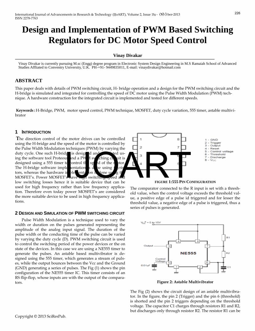
Pulse Width Modulation is a technique used to vary the width or duration on the pulses generated representing the amplitude of the analog input signal. The duration of the pulse width or the conducting time of the pulse can be varied by varying the duty cycle (D). PWM switching circuit is used to control the switching period of the power devices or the on state of the devices. In this case we are using a NE555 timer to generate the pulses. An astable based multivibrator is de-signed using the 555 timer, which generates a stream of puls-es, while the output bounces between the Vcc and the Ground (GND) generating a series of pulses. The Fig (1) shows the pin configuration of the NE555 timer IC. This timer consists of an RS flip-flop, whose inputs are with the output of the compara-tors.
FIGURE 1:555 PIN CONFIGURATION
The comparator connected to the R input is set with a thresh-old value, when the control voltage exceeds the threshold val-ue, a positive edge of a pulse id triggered and for lesser the threshold value, a negative edge of a pulse is triggered, thus a series of pulses is generated.
Figure 2: Astable Multivibrator
The Fig (2) shows the circuit design of an astable multivibra-tor. In the figure, the pin 2 (Trigger) and the pin 6 (threshold) is shorted and the pin 2 triggers depending on the threshold voltage. The capacitor C1 charges through resistors R1 and R2, but discharges only through resistor R2. The resistor R1 can be
226
IJOART
International Journal of Advancements in Research & Technology, Volume 2, Issue ƕƕȮɯ-ÖÝÌÔÉÌÙɪƖƔƕƗ ISSN 2278-7763
Copyright © 2013 SciResPub.
assumed to be a certain value based on which the value of R2 can be set to obtain the particular duty cycle by varying the resistance using a potentiometer.
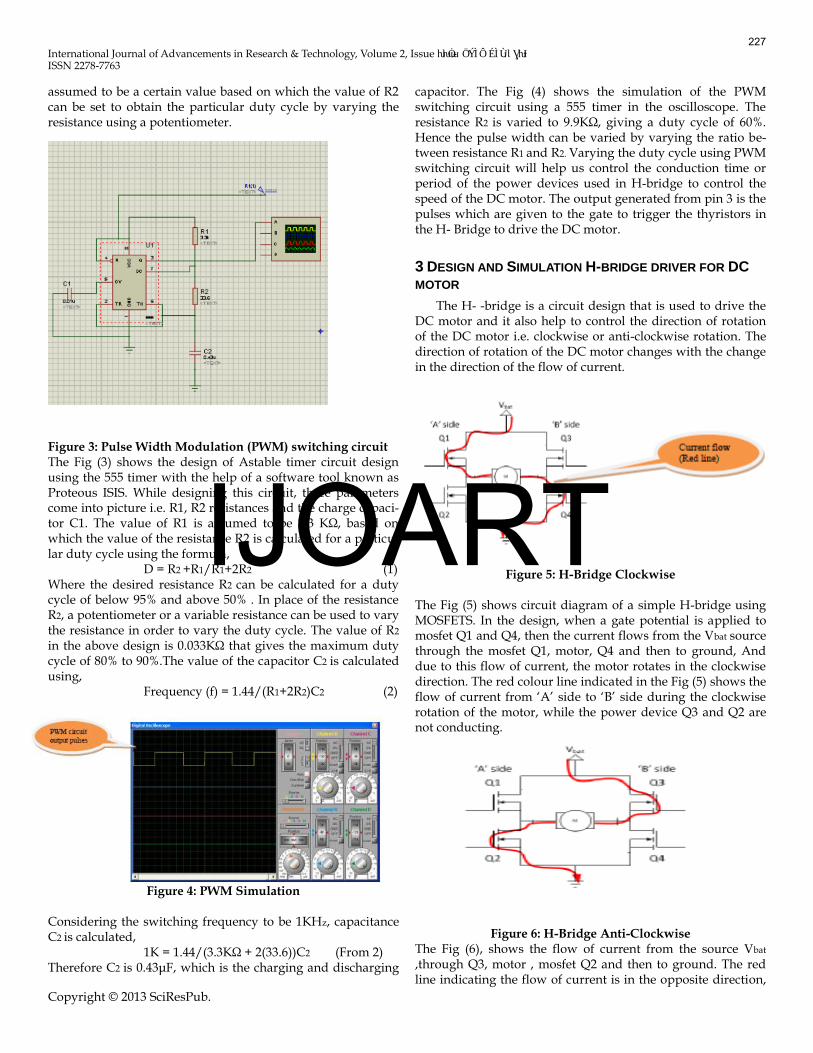
Figure 3: Pulse Width Modulation (PWM) switching circuit The Fig (3) shows the design of Astable timer circuit design using the 555 timer with the help of a software tool known as Proteous ISIS. While designing this circuit, three parameters come into picture i.e. R1, R2 resistances and the charge capaci-tor C1. The value of R1 is assumed to be 3.3 KΩ, based on which the value of the resistance R2 is calculated for a particu-lar duty cycle using the formula,
D = R2 +R1/R1+2R2 (1)
Where the desired resistance R2 can be calculated for a duty cycle of below 95% and above 50% . In place of the resistance R2, a potentiometer or a variable resistance can be used to vary the resistance in order to vary the duty cycle. The value of R2
in the above design is 0.033KΩ that gives the maximum duty cycle of 80% to 90%.The value of the capacitor C2 is calculated using,
Frequency (f) = 1.44/(R1+2R2)C2 (2)
Figure 4: PWM Simulation Considering the switching frequency to be 1KHz, capacitance C2 is calculated,
1K = 1.44/(3.3KΩ + 2(33.6))C2 (From 2)
Therefore C2 is 0.43μF, which is the charging and discharging
capacitor. The Fig (4) shows the simulation of the PWM switching circuit using a 555 timer in the oscilloscope. The resistance R2 is varied to 9.9KΩ, giving a duty cycle of 60%. Hence the pulse width can be varied by varying the ratio be-tween resistance R1 and R2. Varying the duty cycle using PWM switching circuit will help us control the conduction time or period of the power devices used in H-bridge to control the speed of the DC motor. The output generated from pin 3 is the pulses which are given to the gate to trigger the thyristors in the H- Bridge to drive the DC motor.
3 DESIGN AND SIMULATION H-BRIDGE DRIVER FOR DC
MOTOR
The H- -bridge is a circuit design that is used to drive the DC motor and it also help to control the direction of rotation of the DC motor i.e. clockwise or anti-clockwise rotation. The direction of rotation of the DC motor changes with the change in the direction of the flow of current.
Figure 5: H-Bridge Clockwise
The Fig (5) shows circuit diagram of a simple H-bridge using MOSFETS. In the design, when a gate potential is applied to mosfet Q1 and Q4, then the current flows from the Vbat source through the mosfet Q1, motor, Q4 and then to ground, And due to this flow of current, the motor rotates in the clockwise direction. The red colour line indicated in the Fig (5) shows the flow of current from ‘A’ side to ‘B’ side during the clockwise rotation of the motor, while the power device Q3 and Q2 are not conducting.
Figure 6: H-Bridge Anti-Clockwise The Fig (6), shows the flow of current from the source Vbat
,through Q3, motor , mosfet Q2 and then to ground. The red line indicating the flow of current is in the opposite direction,
227
IJOART
International Journal of Advancements in Research & Technology, Volume 2, Issue ƕƕȮɯ-ÖÝÌÔÉÌÙɪƖƔƕƗ ISSN 2278-7763
Copyright © 2013 SciResPub.
thus the motor rotates in the anti-clock wise direction. In this case a get potential is applied to the Q3 and Q2, which con-ducts the current, while the mosfet’s Q1 and Q4 do not con-duct.
Figure 7: H-Bridge Simulation (Clockwise)
The Fig (7) shows the design of an H- bridge using thyristors or silicon controlled rectifiers (SCR) using the software tool proteous ISIS. In the Fig (7), the gates of the thyristors U3 and U5 are shorted, while the gates of the thyristors U4 and U2 are shorted and connected to a diode along with a pull down re-sistor. A pulse generator is used to apply pulses to the gate of the thyristors of U3 and U5, they start conducting, therefore current flows through the DC motor through the switches U3 and U5, thus rotating the motor in clock wise direction. In the Fig (7), diodes D1 and D2 are connected to the gate of the thy-ristors U3 and U2 along with a pull down resistors in order to turn off the SCR and the pull down resistor draws the current to the ground , since once the SCR’s are triggered, it starts conducting even when the gate potential is removed, therefore when the gate potential goes to zero, then if any current flow-ing is grounded by the pull down resistor and a negative spike potential is generated at the falling pulse, in which the poten-tial goes to zero and due to the pull down resistor a negative potential which turns off the SCR’s.
Figure 8: H-Bridge Simulation (Anti-Clockwise)
The Fig (8) shows the spinning of the motor in anti clockwise direction, when the pulse is applied to the gate of the thyris-
tors U2, thus U2 and U4 starts conducting while the thyristors U3 and U5 are reverse biased, hence they are open switch. In this case the current flows in the reverse direction across the load (motor) rotating the motor in opposite direction. There-fore an H-bridge can be modeled and simulated using prote-ous in order to change the spinning direction of the motor and to control its speed using the Astable multivibrator pwm switching.
4 DETERMINATION OF DUTY CYCLES
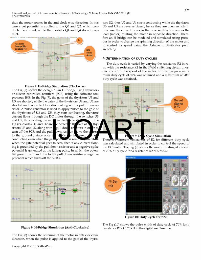
The duty cycle is varied by varying the resistance R2 in ra-tio with the resistance R1 in the PWM switching circuit in or-der to control the speed of the motor. In this design a mini-mum duty cycle of 50% was obtained and a maximum of 90% duty cycle was obtained.
Figure 9: Duty Cycle Simulation Therefore different resistances of R2 for different duty cycle was calculated and simulated in order to control the speed of the DC motor. The Fig (9) shows the motor rotating at a speed of 70% duty cycle for a resistance R2 of 5.75KΩ.
Figure 10: Duty Cycle for 70%
The Fig (10) shows the pulse width of duty cycle of 70% for a resistance R2 of 5.75KΩ in the digital oscilloscope.
228
IJOART
International Journal of Advancements in Research & Technology, Volume 2, Issue ƕƕȮɯ-ÖÝÌÔÉÌÙɪƖƔƕƗ ISSN 2278-7763
Copyright © 2013 SciResPub.
Figure 11: Duty Cycle for 60%
The Fig (11), shows the pulse width of duty cycle of 60% for a resistance R2 of 9.9KΩ or 10KΩ in ratio to the resistance R1 i.e. 3.3KΩ.
Figure 12: Duty Cycle for 90%
The Fig (12) shows the simulation of the pulse width of maxi-mum duty cycle of 90% for a resistance of 0.033KΩ. At this stage the motor was seen to rotate the fastest and beyond which the increase in the duty cycle by varying the variable resistance R2 did not show any increase or difference in the speed of the motor.
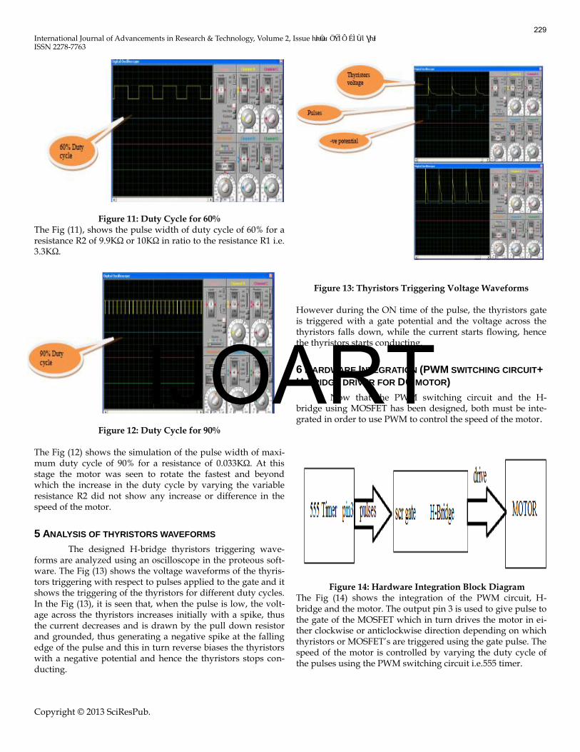
5 ANALYSIS OF THYRISTORS WAVEFORMS
The designed H-bridge thyristors triggering wave-forms are analyzed using an oscilloscope in the proteous soft-ware. The Fig (13) shows the voltage waveforms of the thyris-tors triggering with respect to pulses applied to the gate and it shows the triggering of the thyristors for different duty cycles. In the Fig (13), it is seen that, when the pulse is low, the volt-age across the thyristors increases initially with a spike, thus the current decreases and is drawn by the pull down resistor and grounded, thus generating a negative spike at the falling edge of the pulse and this in turn reverse biases the thyristors with a negative potential and hence the thyristors stops con-ducting.
Figure 13: Thyristors Triggering Voltage Waveforms However during the ON time of the pulse, the thyristors gate is triggered with a gate potential and the voltage across the thyristors falls down, while the current starts flowing, hence the thyristors starts conducting.
6 HARDWARE INTEGRATION (PWM SWITCHING CIRCUIT+
H-BRIDGE DRIVER FOR DC MOTOR)
Now that the PWM switching circuit and the H-bridge using MOSFET has been designed, both must be inte-grated in order to use PWM to control the speed of the motor.
Figure 14: Hardware Integration Block Diagram The Fig (14) shows the integration of the PWM circuit, H-bridge and the motor. The output pin 3 is used to give pulse to the gate of the MOSFET which in turn drives the motor in ei-ther clockwise or anticlockwise direction depending on which thyristors or MOSFET’s are triggered using the gate pulse. The speed of the motor is controlled by varying the duty cycle of the pulses using the PWM switching circuit i.e.555 timer.
229
IJOART
International Journal of Advancements in Research & Technology, Volume 2, Issue ƕƕȮɯ-ÖÝÌÔÉÌÙɪƖƔƕƗ ISSN 2278-7763
Copyright © 2013 SciResPub.
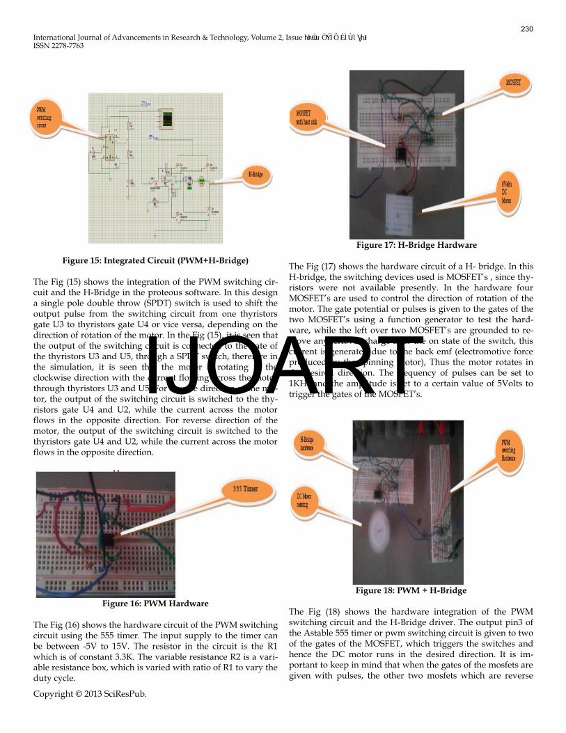
Figure 15: Integrated Circuit (PWM+H-Bridge)
The Fig (15) shows the integration of the PWM switching cir-cuit and the H-Bridge in the proteous software. In this design a single pole double throw (SPDT) switch is used to shift the output pulse from the switching circuit from one thyristors gate U3 to thyristors gate U4 or vice versa, depending on the direction of rotation of the motor. In the Fig (15), it is seen that the output of the switching circuit is connected to the gate of the thyristors U3 and U5, through a SPDT switch, therefore in the simulation, it is seen that the motor is rotating in the clockwise direction with the current flowing across the motor through thyristors U3 and U5. For reverse direction of the mo-tor, the output of the switching circuit is switched to the thy-ristors gate U4 and U2, while the current across the motor flows in the opposite direction. For reverse direction of the motor, the output of the switching circuit is switched to the thyristors gate U4 and U2, while the current across the motor flows in the opposite direction.
Figure 16: PWM Hardware The Fig (16) shows the hardware circuit of the PWM switching circuit using the 555 timer. The input supply to the timer can be between -5V to 15V. The resistor in the circuit is the R1 which is of constant 3.3K. The variable resistance R2 is a vari-able resistance box, which is varied with ratio of R1 to vary the duty cycle.
Figure 17: H-Bridge Hardware
The Fig (17) shows the hardware circuit of a H- bridge. In this H-bridge, the switching devices used is MOSFET’s , since thy-ristors were not available presently. In the hardware four MOSFET’s are used to control the direction of rotation of the motor. The gate potential or pulses is given to the gates of the two MOSFET’s using a function generator to test the hard-ware, while the left over two MOSFET’s are grounded to re-move any leftover charge after the on state of the switch, this current is generated due to the back emf (electromotive force produced by the spinning motor), Thus the motor rotates in the desired direction. The frequency of pulses can be set to 1KHz and the amplitude is set to a certain value of 5Volts to trigger the gates of the MOSFET’s.
Figure 18: PWM + H-Bridge The Fig (18) shows the hardware integration of the PWM switching circuit and the H-Bridge driver. The output pin3 of the Astable 555 timer or pwm switching circuit is given to two of the gates of the MOSFET, which triggers the switches and hence the DC motor runs in the desired direction. It is im-portant to keep in mind that when the gates of the mosfets are given with pulses, the other two mosfets which are reverse
230
IJOART
International Journal of Advancements in Research & Technology, Volume 2, Issue ƕƕȮɯ-ÖÝÌÔÉÌÙɪƖƔƕƗ ISSN 2278-7763
Copyright © 2013 SciResPub.
biased or in off state has to be grounded.
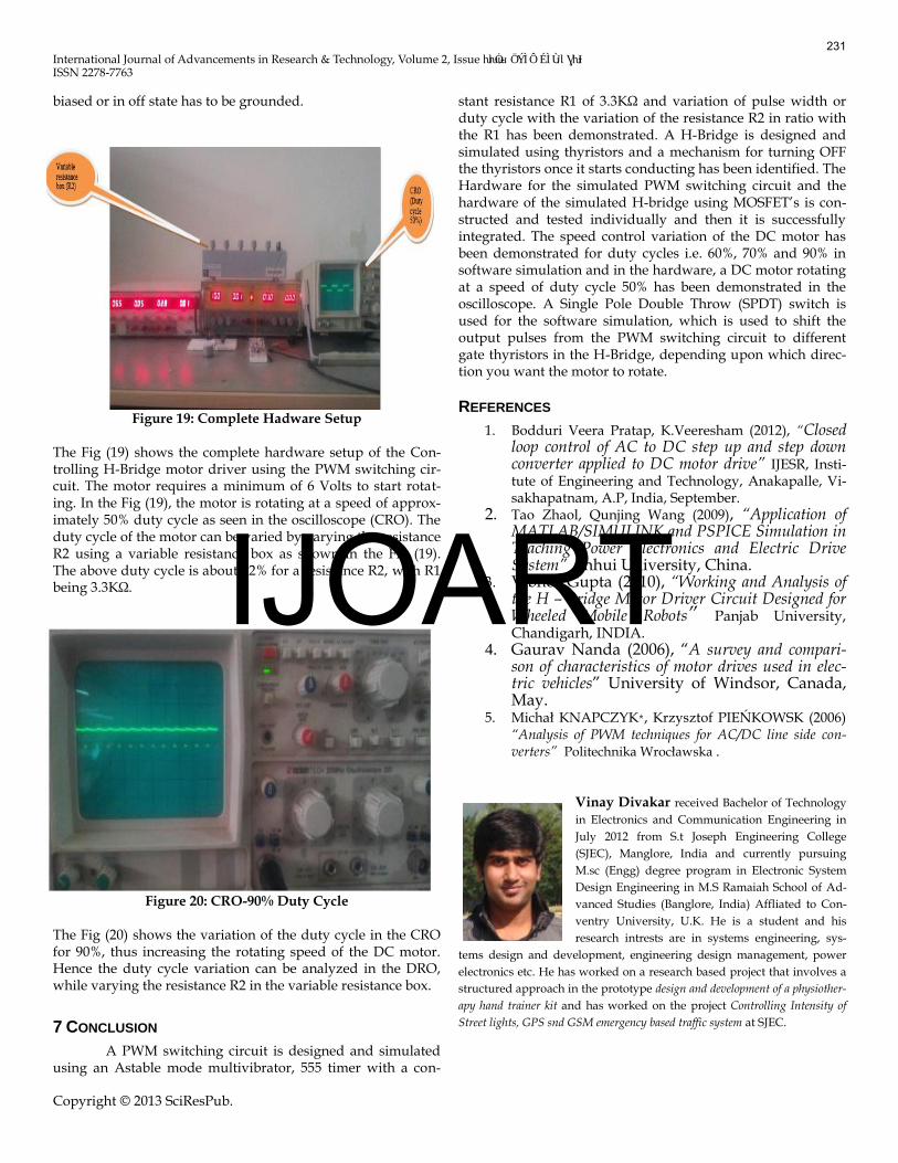
Figure 19: Complete Hadware Setup The Fig (19) shows the complete hardware setup of the Con-trolling H-Bridge motor driver using the PWM switching cir-cuit. The motor requires a minimum of 6 Volts to start rotat-ing. In the Fig (19), the motor is rotating at a speed of approx-imately 50% duty cycle as seen in the oscilloscope (CRO). The duty cycle of the motor can be varied by varying the resistance R2 using a variable resistance box as shown in the Fig (19). The above duty cycle is about 52% for a resistance R2, with R1 being 3.3KΩ.
Figure 20: CRO-90% Duty Cycle The Fig (20) shows the variation of the duty cycle in the CRO for 90%, thus increasing the rotating speed of the DC motor. Hence the duty cycle variation can be analyzed in the DRO, while varying the resistance R2 in the variable resistance box.
7 CONCLUSION
A PWM switching circuit is designed and simulated using an Astable mode multivibrator, 555 timer with a con-
stant resistance R1 of 3.3KΩ and variation of pulse width or duty cycle with the variation of the resistance R2 in ratio with the R1 has been demonstrated. A H-Bridge is designed and simulated using thyristors and a mechanism for turning OFF the thyristors once it starts conducting has been identified. The Hardware for the simulated PWM switching circuit and the hardware of the simulated H-bridge using MOSFET’s is con-structed and tested individually and then it is successfully integrated. The speed control variation of the DC motor has been demonstrated for duty cycles i.e. 60%, 70% and 90% in software simulation and in the hardware, a DC motor rotating at a speed of duty cycle 50% has been demonstrated in the oscilloscope. A Single Pole Double Throw (SPDT) switch is used for the software simulation, which is used to shift the output pulses from the PWM switching circuit to different gate thyristors in the H-Bridge, depending upon which direc-tion you want the motor to rotate.
REFERENCES
1. Bodduri Veera Pratap, K.Veeresham (2012), “Closed loop control of AC to DC step up and step down converter applied to DC motor drive” IJESR, Insti-tute of Engineering and Technology, Anakapalle, Vi-sakhapatnam, A.P, India, September.
2. Tao Zhaol, Qunjing Wang (2009), “Application of MATLAB/SIMULINK and PSPICE Simulation in Teaching Power Electronics and Electric Drive System” Anhui University, China.
3. Vibhor Gupta (2010), “Working and Analysis of the H – Bridge Motor Driver Circuit Designed for Wheeled Mobile Robots” Panjab University, Chandigarh, INDIA.
4. Gaurav Nanda (2006), “A survey and compari-son of characteristics of motor drives used in elec-tric vehicles” University of Windsor, Canada, May.
5. Michał KNAPCZYKF* F, Krzysztof PIEŃKOWSK (2006) “Analysis of PWM techniques for AC/DC line side con-verters” Politechnika Wrocławska .
Vinay Divakar received Bachelor of Technology
in Electronics and Communication Engineering in
July 2012 from S.t Joseph Engineering College
(SJEC), Manglore, India and currently pursuing
M.sc (Engg) degree program in Electronic System
Design Engineering in M.S Ramaiah School of Ad-
vanced Studies (Banglore, India) Affliated to Con-
ventry University, U.K. He is a student and his
research intrests are in systems engineering, sys-
tems design and development, engineering design management, power
electronics etc. He has worked on a research based project that involves a
structured approach in the prototype design and development of a physiother-
apy hand trainer kit and has worked on the project Controlling Intensity of
Street lights, GPS snd GSM emergency based traffic system at SJEC.
231
IJOART