Intel® X38 Express Chipset Datasheet · PDF fileCorporation. No computer system can...
342
Document Number: 317610-001 Intel ® X38 Express Chipset Datasheet — For the Intel ® 82X38 Memory Controller Hub (MCH) October 2007
Transcript of Intel® X38 Express Chipset Datasheet · PDF fileCorporation. No computer system can...

Document Number: 317610-001
Intel® X38 Express Chipset Datasheet
— For the Intel® 82X38 Memory Controller Hub (MCH)
October 2007

2 Datasheet
INFORMATION IN THIS DOCUMENT IS PROVIDED IN CONNECTION WITH INTEL® PRODUCTS. NO LICENSE, EXPRESS OR IMPLIED, BY ESTOPPEL OR OTHERWISE, TO ANY INTELLECTUAL PROPERTY RIGHTS IS GRANTED BY THIS DOCUMENT. EXCEPT AS PROVIDED IN INTEL'S TERMS AND CONDITIONS OF SALE FOR SUCH PRODUCTS, INTEL ASSUMES NO LIABILITY WHATSOEVER, AND INTEL DISCLAIMS ANY EXPRESS OR IMPLIED WARRANTY, RELATING TO SALE AND/OR USE OF INTEL PRODUCTS INCLUDING LIABILITY OR WARRANTIES RELATING TO FITNESS FOR A PARTICULAR PURPOSE, MERCHANTABILITY, OR INFRINGEMENT OF ANY PATENT, COPYRIGHT OR OTHER INTELLECTUAL PROPERTY RIGHT. Intel products are not intended for use in medical, life saving, life sustaining, critical control or safety systems, or in nuclear facility applications.
Intel may make changes to specifications and product descriptions at any time, without notice.
Designers must not rely on the absence or characteristics of any features or instructions marked "reserved" or "undefined." Intel reserves these for future definition and shall have no responsibility whatsoever for conflicts or incompatibilities arising from future changes to them.
The Intel® 82X38Memory Controller Hub (MCH) may contain design defects or errors known as errata, which may cause the product to deviate from published specifications. Current characterized errata are available on request.
Contact your local Intel sales office or your distributor to obtain the latest specifications and before placing your product order.
I2C is a two-wire communications bus/protocol developed by Philips. SMBus is a subset of the I2C bus/protocol and was developed by Intel. Implementations of the I2C bus/protocol may require licenses from various entities, including Philips Electronics N.V. and North American Philips Corporation.
No computer system can provide absolute security under all conditions. Intel® Trusted Execution Technology (Intel® TXT) is a security technology under development by Intel and requires for operation a computer system with Intel® Virtualization Technology, a Intel® Trusted Execution Technology-enabled Intel processor, chipset, BIOS, Authenticated Code Modules, and an Intel or other Intel® Trusted Execution Technology compatible measured virtual machine monitor. In addition, Intel® Trusted Execution Technology requires the system to contain a TPMv1.2 as defined by the Trusted Computing Group and specific software for some uses.
Intel, Pentium, Xeon, and the Intel logo are trademarks or registered trademarks of Intel Corporation or its subsidiaries in the United States and other countries.
*Other names and brands may be claimed as the property of others.
Copyright© 2007, Intel Corporation

Datasheet 3
Contents
1 Introduction ............................................................................................................ 151.1 Terminology ..................................................................................................... 161.2 MCH Overview .................................................................................................. 19
1.2.1 Host Interface........................................................................................ 191.2.2 System Memory Interface ....................................................................... 191.2.3 Direct Media Interface (DMI).................................................................... 201.2.4 PCI Express* Interface............................................................................ 211.2.5 MCH Clocking ........................................................................................ 221.2.6 Power Management ................................................................................ 221.2.7 Thermal Sensor ..................................................................................... 22
2 Signal Description ................................................................................................... 232.1 Host Interface Signals........................................................................................ 242.2 System Memory (DDR2/DDR3) Interface Signals ................................................... 27
2.2.1 System Memory Channel A Interface Signals.............................................. 272.2.2 System Memory Channel B Interface Signals.............................................. 282.2.3 System Memory Miscellaneous Signals ...................................................... 29
2.3 PCI Express* Interface Signals............................................................................ 302.4 Controller Link Interface Signals.......................................................................... 302.5 Clocks, Reset, and Miscellaneous......................................................................... 312.6 Direct Media Interface........................................................................................ 322.7 Power and Grounds ........................................................................................... 32
3 System Address Map ............................................................................................... 333.1 Legacy Address Range ....................................................................................... 36
3.1.1 DOS Range (0h – 9_FFFFh) ..................................................................... 363.1.2 Expansion Area (C_0000h-D_FFFFh) ......................................................... 373.1.3 Extended System BIOS Area (E_0000h–E_FFFFh)....................................... 373.1.4 System BIOS Area (F_0000h–F_FFFFh) ..................................................... 383.1.5 PAM Memory Area Details........................................................................ 38
3.2 Main Memory Address Range (1MB – TOLUD)........................................................ 383.2.1 ISA Hole (15 MB –16 MB)........................................................................ 393.2.2 TSEG.................................................................................................... 403.2.3 Pre-allocated Memory ............................................................................. 40
3.3 PCI Memory Address Range (TOLUD – 4 GB) ........................................................ 413.3.1 APIC Configuration Space (FEC0_0000h–FECF_FFFFh)................................. 433.3.2 HSEG (FEDA_0000h–FEDB_FFFFh) ........................................................... 433.3.3 FSB Interrupt Memory Space (FEE0_0000–FEEF_FFFF)................................ 433.3.4 High BIOS Area...................................................................................... 43
3.4 Main Memory Address Space (4 GB to TOUUD)...................................................... 443.4.1 Memory Re-claim Background.................................................................. 453.4.2 Memory Reclaiming ................................................................................ 45
3.5 PCI Express* Configuration Address Space ........................................................... 453.6 PCI Express* Address Space ............................................................................... 463.7 System Management Mode (SMM)....................................................................... 47
3.7.1 SMM Space Definition ............................................................................. 473.7.2 SMM Space Restrictions .......................................................................... 483.7.3 SMM Space Combinations........................................................................ 483.7.4 SMM Control Combinations ...................................................................... 493.7.5 SMM Space Decode and Transaction Handling ............................................ 493.7.6 Processor WB Transaction to an Enabled SMM Address Space....................... 49

4 Datasheet
3.7.7 SMM Access Through TLB.........................................................................493.8 Memory Shadowing............................................................................................503.9 I/O Address Space .............................................................................................50
3.9.1 PCI Express* I/O Address Mapping............................................................51
4 MCH Register Description.........................................................................................534.1 Register Terminology .........................................................................................544.2 Configuration Process and Registers .....................................................................55
4.2.1 Platform Configuration Structure...............................................................554.3 Configuration Mechanisms ..................................................................................56
4.3.1 Standard PCI Configuration Mechanism......................................................564.3.2 PCI Express Enhanced Configuration Mechanism .........................................57
4.4 Routing Configuration Accesses ...........................................................................584.4.1 Internal Device Configuration Accesses......................................................594.4.2 Bridge Related Configuration Accesses.......................................................60
4.4.2.1 PCI Express Configuration Accesses .............................................604.4.2.2 DMI Configuration Accesses ........................................................60
4.5 I/O Mapped Registers.........................................................................................614.5.1 CONFIG_ADDRESS—Configuration Address Register ....................................614.5.2 CONFIG_DATA—Configuration Data Register ..............................................62
5 DRAM Controller Registers (D0:F0) ..........................................................................635.1 Configuration Register Details..............................................................................65
5.1.1 VID—Vendor Identification .......................................................................655.1.2 DID—Device Identification .......................................................................655.1.3 PCICMD—PCI Command ..........................................................................665.1.4 PCISTS—PCI Status ................................................................................675.1.5 RID—Revision Identification .....................................................................685.1.6 CC—Class Code ......................................................................................685.1.7 MLT—Master Latency Timer......................................................................685.1.8 HDR—Header Type .................................................................................695.1.9 SVID—Subsystem Vendor Identification .....................................................695.1.10 SID—Subsystem Identification..................................................................695.1.11 CAPPTR—Capabilities Pointer....................................................................705.1.12 PXPEPBAR—PCI Express* Egress Port Base Address ....................................705.1.13 MCHBAR—MCH Memory Mapped Register Range Base .................................715.1.14 DEVEN—Device Enable ............................................................................725.1.15 PCIEXBAR—PCI Express* Register Range Base Address ...............................735.1.16 DMIBAR—Root Complex Register Range Base Address .................................755.1.17 PAM0—Programmable Attribute Map 0.......................................................765.1.18 PAM1—Programmable Attribute Map 1.......................................................775.1.19 PAM2—Programmable Attribute Map 2.......................................................785.1.20 PAM3—Programmable Attribute Map 3.......................................................795.1.21 PAM4—Programmable Attribute Map 4.......................................................805.1.22 PAM5—Programmable Attribute Map 5.......................................................815.1.23 PAM6—Programmable Attribute Map 6.......................................................825.1.24 LAC—Legacy Access Control .....................................................................835.1.25 REMAPBASE—Remap Base Address Register...............................................835.1.26 REMAPLIMIT—Remap Limit Address Register ..............................................845.1.27 SMRAM—System Management RAM Control................................................855.1.28 ESMRAMC—Extended System Management RAM Control ..............................865.1.29 TOM—Top of Memory ..............................................................................875.1.30 TOUUD—Top of Upper Usable Dram ..........................................................875.1.31 BSM—Base of Stolen Memory ...................................................................885.1.32 TSEGMB—TSEG Memory Base ..................................................................885.1.33 TOLUD—Top of Low Usable DRAM .............................................................895.1.34 ERRSTS—Error Status .............................................................................905.1.35 ERRCMD—Error Command .......................................................................925.1.36 SMICMD—SMI Command .........................................................................93

Datasheet 5
5.1.37 SKPD—Scratchpad Data .......................................................................... 935.1.38 CAPID0—Capability Identifier ................................................................... 94
5.2 MCHBAR .......................................................................................................... 975.2.1 CHDECMISC—Channel Decode Misc .......................................................... 995.2.2 C0DRB0—Channel 0 DRAM Rank Boundary Address 0 ............................... 1005.2.3 C0DRB1—Channel 0 DRAM Rank Boundary Address 1 ............................... 1015.2.4 C0DRB2—Channel 0 DRAM Rank Boundary Address 2 ............................... 1025.2.5 C0DRB3—Channel 0 DRAM Rank Boundary Address 3 ............................... 1025.2.6 C0DRA01—Channel 0 DRAM Rank 0,1 Attribute ........................................ 1035.2.7 C0DRA23—Channel 0 DRAM Rank 2,3 Attribute ........................................ 1045.2.8 C0CYCTRKPCHG—Channel 0 CYCTRK PCHG ............................................. 1045.2.9 C0CYCTRKACT—Channel 0 CYCTRK ACT .................................................. 1055.2.10 C0CYCTRKWR—Channel 0 CYCTRK WR.................................................... 1065.2.11 C0CYCTRKRD—Channel 0 CYCTRK READ ................................................. 1075.2.12 C0CYCTRKREFR—Channel 0 CYCTRK REFR............................................... 1075.2.13 C0CKECTRL—Channel 0 CKE Control ....................................................... 1085.2.14 C0REFRCTRL—Channel 0 DRAM Refresh Control ....................................... 1095.2.15 C0ECCERRLOG—Channel 0 ECC Error Log................................................ 1115.2.16 C0ODTCTRL—Channel 0 ODT Control ...................................................... 1125.2.17 C1DRB0—Channel 1 DRAM Rank Boundary Address 0 ............................... 1125.2.18 C1DRB1—Channel 1 DRAM Rank Boundary Address 1 ............................... 1135.2.19 C1DRB2—Channel 1 DRAM Rank Boundary Address 2 ............................... 1135.2.20 C1DRB3—Channel 1 DRAM Rank Boundary Address 3 ............................... 1145.2.21 C1DRA01—Channel 1 DRAM Rank 0,1 Attributes....................................... 1145.2.22 C1DRA23—Channel 1 DRAM Rank 2,3 Attributes....................................... 1145.2.23 C1CYCTRKPCHG—Channel 1 CYCTRK PCHG ............................................. 1155.2.24 C1CYCTRKACT—Channel 1 CYCTRK ACT .................................................. 1155.2.25 C1CYCTRKWR—Channel 1 CYCTRK WR.................................................... 1165.2.26 C1CYCTRKRD—Channel 1 CYCTRK READ ................................................. 1175.2.27 C1CKECTRL—Channel 1 CKE Control ....................................................... 1185.2.28 C1REFRCTRL—Channel 1 DRAM Refresh Control ....................................... 1195.2.29 C1ECCERRLOG—Channel 1 ECC Error Log................................................ 1205.2.30 C1ODTCTRL—Channel 1 ODT Control ...................................................... 1215.2.31 EPC0DRB0—EP Channel 0 DRAM Rank Boundary Address 0........................ 1225.2.32 EPC0DRB1—EP Channel 0 DRAM Rank Boundary Address 1........................ 1225.2.33 EPC0DRB2—EP Channel 0 DRAM Rank Boundary Address 2........................ 1225.2.34 EPC0DRB3—EP Channel 0 DRAM Rank Boundary Address 3........................ 1235.2.35 EPC0DRA01—EP Channel 0 DRAM Rank 0,1 Attribute ................................ 1235.2.36 EPC0DRA23—EP Channel 0 DRAM Rank 2,3 Attribute ................................ 1245.2.37 EPDCYCTRKWRTPRE—EPD CYCTRK WRT PRE ........................................... 1245.2.38 EPDCYCTRKWRTACT—EPD CYCTRK WRT ACT ........................................... 1255.2.39 EPDCYCTRKWRTWR—EPD CYCTRK WRT WR............................................. 1255.2.40 EPDCYCTRKWRTREF—EPD CYCTRK WRT REF ........................................... 1265.2.41 EPDCYCTRKWRTRD—EPD CYCTRK WRT READ .......................................... 1265.2.42 EPDCKECONFIGREG—EPD CKE Related Configuration................................ 1275.2.43 EPDREFCONFIG—EP DRAM Refresh Configuration ..................................... 1285.2.44 TSC1—Thermal Sensor Control 1............................................................ 1305.2.45 TSC2—Thermal Sensor Control 2............................................................ 1315.2.46 TSS—Thermal Sensor Status ................................................................. 1335.2.47 TSTTP—Thermal Sensor Temperature Trip Point ....................................... 1345.2.48 TCO—Thermal Calibration Offset ............................................................ 1355.2.49 THERM1—Thermal Hardware Protection................................................... 1365.2.50 TIS—Thermal Interrupt Status ............................................................... 1365.2.51 TSMICMD—Thermal SMI Command......................................................... 1385.2.52 PMSTS—Power Management Status ........................................................ 139
5.3 EPBAR ........................................................................................................... 1405.3.1 EPESD—EP Element Self Description ....................................................... 1405.3.2 EPLE1D—EP Link Entry 1 Description....................................................... 1415.3.3 EPLE1A—EP Link Entry 1 Address ........................................................... 1415.3.4 EPLE2D—EP Link Entry 2 Description....................................................... 142

6 Datasheet
5.3.5 EPLE2A—EP Link Entry 2 Address............................................................1425.3.6 EPLE3D—EP Link Entry 3 Description .......................................................1435.3.7 EPLE3A—EP Link Entry 3 Address............................................................144
6 Host-Primary PCI Express* Bridge Registers (D1:F0) ............................................1456.1 VID1—Vendor Identification ..............................................................................1476.2 DID1—Device Identification...............................................................................1486.3 PCICMD1—PCI Command .................................................................................1486.4 PCISTS1—PCI Status........................................................................................1506.5 RID1—Revision Identification ............................................................................1516.6 CC1—Class Code .............................................................................................1516.7 CL1—Cache Line Size .......................................................................................1526.8 HDR1—Header Type.........................................................................................1526.9 PBUSN1—Primary Bus Number ..........................................................................1526.10 SBUSN1—Secondary Bus Number ......................................................................1536.11 SUBUSN1—Subordinate Bus Number..................................................................1536.12 IOBASE1—I/O Base Address .............................................................................1546.13 IOLIMIT1—I/O Limit Address.............................................................................1546.14 SSTS1—Secondary Status.................................................................................1556.15 MBASE1—Memory Base Address ........................................................................1566.16 MLIMIT1—Memory Limit Address .......................................................................1576.17 PMBASE1—Prefetchable Memory Base Address ....................................................1586.18 PMLIMIT1—Prefetchable Memory Limit Address....................................................1596.19 PMBASEU1—Prefetchable Memory Base Address Upper .........................................1606.20 PMLIMITU1—Prefetchable Memory Limit Address Upper ........................................1616.21 CAPPTR1—Capabilities Pointer ...........................................................................1616.22 INTRLINE1—Interrupt Line................................................................................1626.23 INTRPIN1—Interrupt Pin ...................................................................................1626.24 BCTRL1—Bridge Control ...................................................................................1626.25 PM_CAPID1—Power Management Capabilities ......................................................1646.26 PM_CS1—Power Management Control/Status ......................................................1656.27 SS_CAPID—Subsystem ID and Vendor ID Capabilities ..........................................1666.28 SS—Subsystem ID and Subsystem Vendor ID......................................................1666.29 MSI_CAPID—Message Signaled Interrupts Capability ID........................................1676.30 MC—Message Control .......................................................................................1676.31 MA—Message Address ......................................................................................1686.32 MD—Message Data ..........................................................................................1686.33 PE_CAPL—PCI Express* Capability List ...............................................................1686.34 PE_CAP—PCI Express* Capabilities ....................................................................1696.35 DCAP—Device Capabilities ................................................................................1696.36 DCTL—Device Control.......................................................................................1706.37 DSTS—Device Status .......................................................................................1716.38 LCAP—Link Capabilities.....................................................................................1726.39 LCTL—Link Control...........................................................................................1746.40 LSTS—Link Status............................................................................................1766.41 SLOTCAP—Slot Capabilities ...............................................................................1776.42 SLOTCTL—Slot Control .....................................................................................1786.43 SLOTSTS—Slot Status ......................................................................................1806.44 RCTL—Root Control..........................................................................................1816.45 RSTS—Root Status ..........................................................................................1826.46 PELC—PCI Express Legacy Control .....................................................................1826.47 VCECH—Virtual Channel Enhanced Capability Header............................................1836.48 PVCCAP1—Port VC Capability Register 1 .............................................................1836.49 PVCCAP2—Port VC Capability Register 2 .............................................................1846.50 PVCCTL—Port VC Control ..................................................................................1846.51 VC0RCAP—VC0 Resource Capability ...................................................................1856.52 VC0RCTL—VC0 Resource Control .......................................................................1866.53 VC0RSTS—VC0 Resource Status ........................................................................1876.54 RCLDECH—Root Complex Link Declaration Enhanced ............................................1876.55 ESD—Element Self Description ..........................................................................188

Datasheet 7
6.56 LE1D—Link Entry 1 Description ......................................................................... 1886.57 LE1A—Link Entry 1 Address .............................................................................. 1896.58 PESSTS—PCI Express* Sequence Status ............................................................ 189
7 Intel Manageability Engine Subsystem PCI (D3:F0,F3) .......................................... 1917.1 HECI Function in ME Subsystem (D3:F0) ............................................................ 191
7.1.1 ID—Identifiers ..................................................................................... 1927.1.2 CMD—Command .................................................................................. 1927.1.3 STS—Device Status .............................................................................. 1937.1.4 RID—Revision ID.................................................................................. 1937.1.5 CC—Class Code.................................................................................... 1937.1.6 CLS—Cache Line Size............................................................................ 1947.1.7 MLT—Master Latency Timer ................................................................... 1947.1.8 HTYPE—Header Type ............................................................................ 1947.1.9 HECI_MBAR—HECI MMIO Base Address................................................... 1957.1.10 SS—Sub System Identifiers ................................................................... 1957.1.11 CAP—Capabilities Pointer....................................................................... 1967.1.12 INTR—Interrupt Information .................................................................. 1967.1.13 MGNT—Minimum Grant ......................................................................... 1967.1.14 MLAT—Maximum Latency ...................................................................... 1977.1.15 HFS—Host Firmware Status ................................................................... 1977.1.16 PID—PCI Power Management Capability ID .............................................. 1977.1.17 PC—PCI Power Management Capabilities ................................................. 1987.1.18 PMCS—PCI Power Management Control And Status................................... 1987.1.19 MID—Message Signaled Interrupt Identifiers ............................................ 1997.1.20 MC—Message Signaled Interrupt Message Control..................................... 1997.1.21 MA—Message Signaled Interrupt Message Address.................................... 2007.1.22 MUA—Message Signaled Interrupt Upper Address (Optional) ...................... 2007.1.23 MD—Message Signaled Interrupt Message Data........................................ 2007.1.24 HIDM—HECI Interrupt Delivery Mode ...................................................... 201
7.2 KT IO/ Memory Mapped Device Specific Registers [D3:F3] .................................... 2027.2.1 KTRxBR—KT Receive Buffer .................................................................. 2027.2.2 KTTHR—KT Transmit Holding ................................................................ 2037.2.3 KTDLLR—KT Divisor Latch LSB .............................................................. 2037.2.4 KTIER—KT Interrupt Enable .................................................................. 2047.2.5 KTDLMR—KT Divisor Latch MSB ............................................................. 2047.2.6 KTIIR—KT Interrupt Identification .......................................................... 2057.2.7 KTFCR—KT FIFO Control ....................................................................... 2067.2.8 KTLCR—KT Line Control ....................................................................... 2077.2.9 KTMCR—KT Modem Control .................................................................. 2087.2.10 KTLSR—KT Line Status ......................................................................... 2097.2.11 KTMSR—KT Modem Status ................................................................... 2107.2.12 KTSCR—KT Scratch ............................................................................. 210
8 Host-Secondary PCI Express* Bridge Registers (D6:F0) ....................................... 2118.1 VID1—Vendor Identification.............................................................................. 2138.2 DID1—Device Identification .............................................................................. 2148.3 PCICMD1—PCI Command ................................................................................. 2148.4 PCISTS1—PCI Status ....................................................................................... 2168.5 RID1—Revision Identification ............................................................................ 2178.6 CC1—Class Code ............................................................................................. 2178.7 CL1—Cache Line Size....................................................................................... 2188.8 HDR1—Header Type ........................................................................................ 2188.9 PBUSN1—Primary Bus Number.......................................................................... 2188.10 SBUSN1—Secondary Bus Number...................................................................... 2198.11 SUBUSN1—Subordinate Bus Number ................................................................. 2198.12 IOBASE1—I/O Base Address ............................................................................. 2208.13 IOLIMIT1—I/O Limit Address ............................................................................ 2208.14 SSTS1—Secondary Status ................................................................................ 2218.15 MBASE1—Memory Base Address........................................................................ 222
8 Datasheet
8.16 MLIMIT1—Memory Limit Address .......................................................................2238.17 PMBASE1—Prefetchable Memory Base Address Upper ...........................................2248.18 PMLIMIT1—Prefetchable Memory Limit Address....................................................2258.19 PMBASEU1—Prefetchable Memory Base Address Upper .........................................2268.20 PMLIMITU1—Prefetchable Memory Limit Address Upper ........................................2278.21 CAPPTR1—Capabilities Pointer ...........................................................................2288.22 INTRLINE1—Interrupt Line................................................................................2288.23 INTRPIN1—Interrupt Pin ...................................................................................2288.24 BCTRL1—Bridge Control ...................................................................................2298.25 PM_CAPID1—Power Management Capabilities ......................................................2308.26 PM_CS1—Power Management Control/Status ......................................................2318.27 SS_CAPID—Subsystem ID and Vendor ID Capabilities ..........................................2328.28 SS—Subsystem ID and Subsystem Vendor ID......................................................2328.29 MSI_CAPID—Message Signaled Interrupts Capability ID........................................2338.30 MC—Message Control .......................................................................................2338.31 MA—Message Address ......................................................................................2348.32 MD—Message Data ..........................................................................................2348.33 PE_CAPL—PCI Express* Capability List ...............................................................2348.34 PE_CAP—PCI Express* Capabilities ....................................................................2358.35 DCAP—Device Capabilities ................................................................................2358.36 DCTL—Device Control.......................................................................................2368.37 DSTS—Device Status .......................................................................................2378.38 LCAP—Link Capabilities.....................................................................................2388.39 LCTL—Link Control...........................................................................................2408.40 LSTS—Link Status............................................................................................2428.41 SLOTCAP—Slot Capabilities ...............................................................................2438.42 SLOTCTL—Slot Control .....................................................................................2448.43 SLOTSTS—Slot Status ......................................................................................2468.44 RCTL—Root Control..........................................................................................2478.45 RSTS—Root Status ..........................................................................................2488.46 PELC—PCI Express Legacy Control .....................................................................2488.47 VCECH—Virtual Channel Enhanced Capability Header............................................2498.48 PVCCAP1—Port VC Capability Register 1 .............................................................2498.49 PVCCAP2—Port VC Capability Register 2 .............................................................2508.50 PVCCTL—Port VC Control ..................................................................................2508.51 VC0RCAP—VC0 Resource Capability ...................................................................2518.52 VC0RCTL—VC0 Resource Control .......................................................................2528.53 VC0RSTS—VC0 Resource Status ........................................................................2538.54 RCLDECH—Root Complex Link Declaration Enhanced ............................................2538.55 ESD—Element Self Description ..........................................................................2548.56 LE1D—Link Entry 1 Description..........................................................................2558.57 LE1A—Link Entry 1 Address ..............................................................................255
9 Direct Media Interface (DMI) RCRB........................................................................2579.1 DMIVCECH—DMI Virtual Channel Enhanced Capability ..........................................2589.2 DMIPVCCAP1—DMI Port VC Capability Register 1 .................................................2589.3 DMIPVCCTL—DMI Port VC Control ......................................................................2599.4 DMIVC0RCAP—DMI VC0 Resource Capability .......................................................2599.5 DMIVC0RCTL0—DMI VC0 Resource Control .........................................................2609.6 DMIVC0RSTS—DMI VC0 Resource Status ............................................................2619.7 DMIVC1RCAP—DMI VC1 Resource Capability .......................................................2619.8 DMIVC1RCTL1—DMI VC1 Resource Control .........................................................2629.9 DMIVC1RSTS—DMI VC1 Resource Status ............................................................2639.10 DMILCAP—DMI Link Capabilities ........................................................................2639.11 DMILCTL—DMI Link Control...............................................................................2649.12 DMILSTS—DMI Link Status ...............................................................................264

Datasheet 9
10 Functional Description ........................................................................................... 26510.1 Host Interface................................................................................................. 265
10.1.1 FSB IOQ Depth .................................................................................... 26510.1.2 FSB OOQ Depth ................................................................................... 26510.1.3 FSB GTL+ Termination.......................................................................... 26510.1.4 FSB Dynamic Bus Inversion ................................................................... 26510.1.5 APIC Cluster Mode Support.................................................................... 266
10.2 System Memory Controller ............................................................................... 26710.2.1 System Memory Organization Modes....................................................... 267
10.2.1.1 Single Channel Mode ............................................................... 26710.2.1.2 Dual Channel Modes................................................................ 267
10.2.2 System Memory Technology Supported ................................................... 26910.2.3 Error Checking and Correction................................................................ 270
10.3 PCI Express* .................................................................................................. 27310.3.1 PCI Express* Architecture ..................................................................... 273
10.3.1.1 Transaction Layer ................................................................... 27310.3.1.2 Data Link Layer ...................................................................... 27310.3.1.3 Physical Layer ........................................................................ 273
10.4 Thermal Sensor............................................................................................... 27410.4.1 PCI Device 0, Function 0 ....................................................................... 27410.4.2 MCHBAR Thermal Sensor Registers......................................................... 274
10.5 Power Management ......................................................................................... 27510.6 Clocking......................................................................................................... 275
11 Electrical Characteristics ....................................................................................... 27711.1 Absolute Minimum and Maximum Ratings ........................................................... 27711.2 Current Consumption....................................................................................... 27911.3 Signal Groups ................................................................................................. 28011.4 Buffer Supply and DC Characteristics ................................................................. 283
11.4.1 I/O Buffer Supply Voltages .................................................................... 28311.4.2 General DC Characteristics .................................................................... 284
12 Ballout and Package Information........................................................................... 28712.1 Ballout Information.......................................................................................... 28712.2 Package Information........................................................................................ 311
13 Testability ............................................................................................................. 31313.1 XOR Test Mode Initialization ............................................................................. 31313.2 XOR Chain Definition ....................................................................................... 31413.3 XOR Chains .................................................................................................... 315
13.3.1 XOR Chains for DDR2 (No ECC).............................................................. 31613.3.2 XOR Chains for DDR2 (ECC) .................................................................. 32513.3.3 XOR Chains for DDR3 (No ECC).............................................................. 334

10 Datasheet
Figures1 Intel® X38 Express Chipset System Diagram Example ...................................................162 System Address Ranges ............................................................................................353 DOS Legacy Address Range .......................................................................................364 Main Memory Address Range .....................................................................................395 Pre-allocated Memory Example for 64 MB DRAM, 1 MB stolen and 1 MB TSEG...................406 PCI Memory Address Range ......................................................................................427 Conceptual Platform PCI Configuration Diagram............................................................558 Memory Map to PCI Express Device Configuration Space................................................589 MCH Configuration Cycle Flow Chart............................................................................5910 System Clocking Diagram........................................................................................27611 MCH Ballout Diagram (Top View Left – Columns 45–31) ..............................................28812 MCH Ballout Diagram (Top View Middle – Columns 30–16)...........................................28913 MCH Ballout Diagram (Top View Left – Columns 15–1) ................................................29014 MCH Package Drawing ............................................................................................31115 XOR Test Mode Initialization Cycles...........................................................................313
Tables1 Intel Specification.....................................................................................................182 Expansion Area Memory Segments .............................................................................373 Extended System BIOS Area Memory Segments ...........................................................374 System BIOS Area Memory Segments .........................................................................385 Transaction Address Ranges – Compatible, High, and TSEG............................................476 SMM Space Table .....................................................................................................487 SMM Control Table....................................................................................................498 DRAM Controller Register Address Map........................................................................639 MCHBAR Register Address Map...................................................................................9710 DRAM Rank Attribute Register Programming ..............................................................10311 EPBAR Address Map................................................................................................14012 Host-PCI Express Bridge Register Address Map (D1:F0) ...............................................14513 HECI Function in ME Subsystem (D3:F0) Register Address Map ....................................19114 KT IO/Memory Mapped Register Address Map.............................................................20215 Host-Secondary PCI Express* Bridge Register Address Map (D6:F0)..............................21116 Direct Media Interface Register Address Map ..............................................................25717 Host Interface 4X, 2X, and 1X Signal Groups..............................................................26618 Sample System Memory Dual Channel Symmetric Organization Mode............................26719 Sample System Memory Dual Channel Asymmetric Organization Mode with
Intel® Flex Memory Mode Enabled ............................................................................26820 Sample System Memory Dual Channel Asymmetric Organization Mode with
Intel® Flex Memory Mode Disabled ...........................................................................26821 Supported DIMM Module Configurations.....................................................................26922 Syndrome Bit Values...............................................................................................27023 Absolute Minimum and Maximum Ratings ..................................................................27724 Current Consumption in S0......................................................................................27925 Signal Groups ........................................................................................................28126 I/O Buffer Supply Voltage........................................................................................28327 DC Characteristics ..................................................................................................28428 MCH Ballout Sorted By Name ...................................................................................29129 MCH Ballout Sorted By Ball ......................................................................................30130 XOR Chain 14 Functionality......................................................................................31431 XOR Chain Outputs.................................................................................................31532 XOR Chain 0 (DDR2, NoECC) ...................................................................................31633 XOR Chain 1 (DDR2, NoECC) ...................................................................................31634 XOR Chain 2 (DDR2, NoECC) ...................................................................................317
Datasheet 11
35 XOR Chain 3 (DDR2, NoECC) ................................................................................... 31736 XOR Chain 4 (DDR2, NoECC) ................................................................................... 31837 XOR Chain 5 (DDR2, NoECC) ................................................................................... 31838 XOR Chain 6 (DDR2, NoECC) ................................................................................... 31839 XOR Chain 7 (DDR2, NoECC) ................................................................................... 31940 XOR Chain 8 (DDR2, NoECC) ................................................................................... 32041 XOR Chain 9 (DDR2, NoECC) ................................................................................... 32042 XOR Chain 10 (DDR2, NoECC) ................................................................................. 32043 XOR Chain 11 (DDR2, NoECC) ................................................................................. 32144 XOR Chain 12 (DDR2, NoECC) ................................................................................. 32245 XOR Chain 13 (DDR2, NoECC) ................................................................................. 32246 XOR Chain 14 (DDR2, NoECC) ................................................................................. 32347 XOR Chain 0 (DDR2, ECC)....................................................................................... 32548 XOR Chain 1 (DDR2, ECC)....................................................................................... 32649 XOR Chain 2 (DDR2, ECC)....................................................................................... 32650 XOR Chain 3 (DDR2, ECC)....................................................................................... 32651 XOR Chain 4 (DDR2, ECC)....................................................................................... 32752 XOR Chain 5 (DDR2, ECC)....................................................................................... 32753 XOR Chain 6 (DDR2, ECC)....................................................................................... 32854 XOR Chain 7 (DDR2, ECC)....................................................................................... 32955 XOR Chain 8 (DDR2, ECC)....................................................................................... 32956 XOR Chain 9 (DDR2, ECC)....................................................................................... 32957 XOR Chain 10 (DDR2, ECC) ..................................................................................... 33058 XOR Chain 11 (DDR2, ECC) ..................................................................................... 33159 XOR Chain 12 (DDR2, ECC) ..................................................................................... 33160 XOR Chain 13 (DDR2, ECC) ..................................................................................... 33161 XOR Chain 14 (DDR2, ECC) ..................................................................................... 33262 XOR Chain 0 (DDR3, NoECC) ................................................................................... 33463 XOR Chain 1 (DDR3, NoECC) ................................................................................... 33464 XOR Chain 2 (DDR3, NoECC) ................................................................................... 33565 XOR Chain 3 (DDR3, NoECC) ................................................................................... 33566 XOR Chain 4 (DDR3, NoECC) ................................................................................... 33667 XOR Chain 5 (DDR3, NoECC) ................................................................................... 33668 XOR Chain 6 (DDR3, NoECC) ................................................................................... 33669 XOR Chain 7 (DDR3, NoECC) ................................................................................... 33770 XOR Chain 8 (DDR3, NoECC) ................................................................................... 33871 XOR Chain 9 (DDR3, NoECC) ................................................................................... 33872 XOR Chain 10 (DDR3, NoECC) ................................................................................. 33873 XOR Chain 11 (DDR3, NoECC) ................................................................................. 33974 XOR Chain 12 (DDR3, NoECC) ................................................................................. 34075 XOR Chain 13 (DDR3, NoECC) ................................................................................. 34076 XOR Chain 14 (DDR3, NoECC) ................................................................................. 341

12 Datasheet
Revision History
Revision Number Description Revision Date
-001 • Initial release October 2007

Datasheet 13
Intel® 82X38 MCH Features
§
• Processor/Host Interface (FSB) — Supports Intel® Core™2 Duo desktop processor— Supports Intel® Core™2 Quad desktop processor— 800/1067/1333 MT/s (200/266/333 MHz) FSB— Hyper-Threading Technology (HT Technology)— FSB Dynamic Bus Inversion (DBI)— 36-bit host bus addressing— 12-deep In-Order Queue — 1-deep Defer Queue— GTL+ bus driver with integrated GTL termination resistors— Supports cache Line Size of 64 bytes
• System Memory Interface — One or two channels (each channel consisting of 64 data lines)— Single or Dual Channel memory organization— DDR2-800/667 frequencies— DDR3-1066/800 frequencies — Unbuffered, ECC and non-ECC DDR2 or non-ECC DDR3 DIMMs— Supports 1-Gb, 512-Mb DDR2 or DDR3 technologies for x8 and
x16 devices— 8 GB maximum memory
• Direct Media Interface (DMI)— Chip-to-chip connection interface to Intel ICH9 — 2 GB/s point-to-point DMI to ICH9 (1 GB/s each direction)— 100 MHz reference clock (shared with PCI Express graphics
attach)— 32-bit downstream addressing— Messaging and Error Handling
• PCI Express* Interface— Two x16 PCI Express ports — Compatible with the PCI Express Base Specification,
Revision 2.0— Raw bit rate on data pins of 5 Gb/s resulting in a real
bandwidth per pair of 500 MB/s • Thermal Sensor
— Catastrophic Trip Point support — Hot Trip Point support for SMI generation
• Power Management— PC99 suspend to DRAM support (“STR”, mapped to
ACPI state S3)— ACPI Revision 2.0 compatible power management— Supports processor states: C0, C1, C2— Supports System states: S0, S1, S3 (Cold), and S5— Supports processor Thermal Management 2
• Package— FC-BGA— 40 mm × 40 mm package size— 1300 balls, located in a non-grid pattern

14 Datasheet

Datasheet 15
Introduction
1 Introduction
The Intel® X38 Express Chipset is designed for use with the Intel® CoreTM2 Duo processor and Intel® Core™2 Quad processor in high-end desktop and workstation platforms. The chipset contains two components: 82X38 MCH for the host bridge and I/O Controller Hub 9 (ICH9) for the I/O subsystem. The ICH9 is the ninth generation I/O Controller Hub and provides a multitude of I/O related functions. Figure 1 shows an example system block diagram for the Intel® X38 Express Chipset.
This document is the datasheet for the Intel® 82X38 Memory Controller Hub (MCH). Topics covered include; signal description, system memory map, PCI register description, a description of the MCH interfaces and major functional units, electrical characteristics, ballout definitions, and package characteristics.
Note: Unless otherwise specified, ICH9 refers to the Intel® 82801IB ICH9 and Intel® 82801IR ICH9R I/O Controller Hub 9 components.
Note: The term ICH9 refers to the ICH9 and ICH9R components.
Introduction
16 Datasheet
1.1 TerminologyFigure 1. Intel® X38 Express Chipset System Diagram Example
Term Description
Chipset / Root – Complex
Used in this specification to refer to one or more hardware components that connect processor complexes to the I/O and memory subsystems. The chipset may include a variety of integrated devices.
CLinkController Link is a proprietary chip-to-chip connection between the MCH and ICH. The chipset requires that Clink is connected in the platform.
Core The internal base logic in the MCH
DBI Dynamic Bus Inversion
DDR2 A second generation Double Data Rate SDRAM memory technology
DDR3 A third generation Double Data Rate SDRAM memory technology
C Link – Still connect on non-
AMT systemDMI
PCI ExpressPCI Express x16
USB 2. 0 12 Ports
GPIO
SATA 6 Ports
Firmware
SIO
Power Management
Clock Generation
SMBus 2.0 / I2C
SST/PECI (Fan Speed Control)
Gb LAN
WLAN
PCIe Bus
6 PCIe x1 Slots
PCI Bus4 PCI Masters
Intel® ICH 9
Intel® 82X38MCH
Processor
SPIFlash
SPI
LPC
PCI ExpressPCI Express x16
DDR2/3DDR2 /DDR3
DDR2/3
System Memory
CH A
CH B DDR2 /DDR3

Datasheet 17
Introduction
DMIDirect Media Interface is a proprietary chip-to-chip connection between the MCH and ICH. This interface is based on the standard PCI Express* specification.
DomainA collection of physical, logical or virtual resources that are allocated to work together. Domain is used as a generic term for virtual machines, partitions, etc.
EP PCI Express Egress Port
FSB Front Side Bus. Synonymous with Host or processor bus
Full ResetFull reset is when PWROK is de-asserted. Warm reset is when both RSTIN# and PWROK are asserted.
MCHMemory Controller Hub component that contains the processor interface, DRAM controller, and PCI Express port. It communicates with the I/O controller hub (Intel® ICH9) over the DMI interconnect. .
Host This term is used synonymously with processor
INTx An interrupt request signal where X stands for interrupts A, B, C and D
Intel® ICH9Ninth generation I/O Controller Hub component that contains the primary PCI interface, LPC interface, USB2.0, SATA, and other I/O functions. For this MCH, the term ICH refers to the ICH9.
IOQ In Order Queue
MSIMessage Signaled Interrupt. A transaction conveying interrupt information to the receiving agent through the same path that normally carries read and write commands.
OOQ Out of Order Queueing
PCI Express*A high-speed serial interface whose configuration is software compatible with the legacy PCI specifications.
Primary PCI The physical PCI bus that is driven directly by the Intel® ICH9. Communication between Primary PCI and the MCH occurs over DMI. The Primary PCI bus is not PCI Bus 0 from a configuration standpoint.
RankA unit of DRAM corresponding to eight x8 SDRAM devices in parallel or four x16 SDRAM devices in parallel, ignoring ECC. These devices are usually, but not always, mounted on a single side of a DIMM.
SCI System Control Interrupt. Used in ACPI protocol.
SERRSystem Error. An indication that an unrecoverable error has occurred on an I/O bus.
SMI
System Management Interrupt. Used to indicate any of several system conditions such as thermal sensor events, throttling activated, access to System Management RAM, chassis open, or other system state related activity.
Intel® TXTIntel® Trusted Execution Technology (TXT) defines platform level enhancements that provide the building blocks for creating trusted platforms.
VCO Voltage Controlled Oscillator
Term Description
Introduction
18 Datasheet
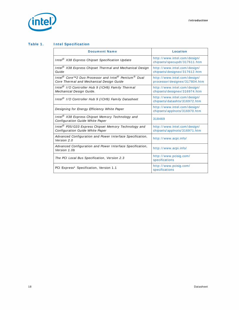
Table 1. Intel Specification
Document Name Location
Intel® X38 Express Chipset Specification Updatehttp://www.intel.com/design/chipsets/specupdt/317611.htm
Intel® X38 Express Chipset Thermal and Mechanical Design Guide
http://www.intel.com/design/chipsets/designex/317612.htm
Intel® Core™2 Duo Processor and Intel® Pentium® Dual Core Thermal and Mechanical Design Guide
http://www.intel.com/design/processor/designex/317804.htm
Intel® I/O Controller Hub 9 (ICH9) Family Thermal Mechanical Design Guide.
http://www.intel.com/design/chipsets/designex/316974.htm
Intel® I/O Controller Hub 9 (ICH9) Family Datasheethttp://www.intel.com/design/chipsets/datashts/316972.htm
Designing for Energy Efficiency White Paperhttp://www.intel.com/design/chipsets/applnots/316970.htm
Intel® X38 Express Chipset Memory Technology and Configuration Guide White Paper
318469
Intel® P35/G33 Express Chipset Memory Technology and Configuration Guide White Paper
http://www.intel.com/design/chipsets/applnots/316971.htm
Advanced Configuration and Power Interface Specification, Version 2.0
http://www.acpi.info/
Advanced Configuration and Power Interface Specification, Version 1.0b
http://www.acpi.info/
The PCI Local Bus Specification, Version 2.3 http://www.pcisig.com/specifications
PCI Express* Specification, Version 1.1http://www.pcisig.com/specifications

Datasheet 19
Introduction
1.2 MCH Overview
The role of a MCH in a system is to manage the flow of information between its four interfaces: the processor interface, the system memory interface, the PCI Express interface, and the I/O Controller through DMI interface. This includes arbitrating between the four interfaces when each initiates transactions. It supports one or two channels of DDR2 or DDR3 SDRAM. It also supports the PCI Express based external device attach. The Intel X38 Express Chipset platform supports the ninth generation I/O Controller Hub (Intel ICH9) to provide I/O related features.
1.2.1 Host Interface
The MCH supports a single LGA775 socket processor. The MCH supports a FSB frequency of 800/1066/1333 MHz. Host-initiated I/O cycles are decoded to PCI Express, DMI, or the MCH configuration space. Host-initiated memory cycles are decoded to PCI Express, DMI or system memory. PCI Express device accesses to non-cacheable system memory are not snooped on the host bus. Memory accesses initiated from PCI Express using PCI semantics and from DMI to system SDRAM will be snooped on the host bus.
Processor/Host Interface (FSB) Details
• Supports the Intel® CoreTM2 Duo processor and Intel® Core™2 Quad processor
• Supports Front Side Bus (FSB) at the following Frequency Ranges:
— 800/1066/1333MT/s
• Supports FSB Dynamic Bus Inversion (DBI)
• Supports 36-bit host bus addressing, allowing the processor to access the entire 64 GB of the host address space.
• Has a 12-deep In-Order Queue to support up to twelve outstanding pipelined address requests on the host bus
• Has a 1-deep Defer Queue
• Uses GTL+ bus driver with integrated GTL termination resistors
• Supports a Cache Line Size of 64 bytes
1.2.2 System Memory Interface
The MCH integrates a system memory DDR2/DDR3 controller with two, 64-bit wide interfaces. The buffers support both SSTL_1.8 (Stub Series Terminated Logic for 1.8 V) and SSTL_1.5 (Stub Series Terminated Logic for 1.5 V) signal interfaces. The memory controller interface is fully configurable through a set of control registers.
System Memory Interface Details
• Directly supports one or two channels of DDR2 or DDR3 memory with a maximum of two DIMMs per channel.
• Supports single and dual channel memory organization modes.
• Supports a data burst length of eight for all memory organization modes.
• Supports memory data transfer rates of 667 and 800 MHz for DDR2 and 800, 1066, and 1333 MHz for DDR3.
• I/O Voltage of 1.8 V for DDR2 and 1.5 V for DDR3.
• Supports both un-buffered ECC and non-ECC DDR2 or non-ECC DDR3 DIMMs.

Introduction
20 Datasheet
• Supports maximum memory bandwidth of 6.4 GB/s in single-channel mode or 12.8 GB/s in dual-channel mode assuming DDR2 800 MHz.
• Supports maximum memory bandwidth of 10.6GB/s in single-channel mode or 21 GB/s in dual-channel mode assuming DDR3 1333 MHz.
• Supports 512-Mb and 1-Gb DDR2 or DDR3 DRAM technologies for x8 and x16 devices.
• Using 512 Mb device technologies, the smallest memory capacity possible is 256 MB, assuming Single Channel Mode with a single x16 single sided un-buffered non-ECC DIMM memory configuration.
• Using 1 Gb device technologies, the largest memory capacity possible is 8 GB, assuming Dual Channel Mode with four x8 double sided un-buffered non-ECC or ECC DIMM memory configurations. Note: The ability to support greater than the largest memory capacity is subject to availability of higher density memory devices.
• Supports up to 32 simultaneous open pages per channel (assuming 4 ranks of 8 bank devices)
• Supports opportunistic refresh scheme
• Supports Partial Writes to memory using Data Mask (DM) signals
• Supports a memory thermal management scheme to selectively manage reads and/or writes. Memory thermal management can be triggered either by on-die thermal sensor, or by preset limits. Management limits are determined by weighted sum of various commands that are scheduled on the memory interface.
1.2.3 Direct Media Interface (DMI)
Direct Media Interface (DMI) is the chip-to-chip connection between the MCH and ICH9. This high-speed interface integrates advanced priority-based servicing allowing for concurrent traffic and true isochronous transfer capabilities. Base functionality is completely software transparent permitting current and legacy software to operate normally.
To provide for true isochronous transfers and configurable Quality of Service (QoS) transactions, the ICH9 supports two virtual channels on DMI: VC0 and VC1. These two channels provide a fixed arbitration scheme where VC1 is always the highest priority. VC0 is the default conduit of traffic for DMI and is always enabled. VC1 must be specifically enabled and configured at both ends of the DMI link (i.e., the ICH9 and MCH).
• A chip-to-chip connection interface to Intel ICH9 • 2 GB/s point-to-point DMI to ICH9 (1 GB/s each direction)• 100 MHz reference clock (shared with PCI Express)• 32-bit downstream addressing• APIC and MSI interrupt messaging support. Will send Intel-defined “End Of
Interrupt” broadcast message when initiated by the processor.• Message Signaled Interrupt (MSI) messages• SMI, SCI, and SERR error indication

Datasheet 21
Introduction
1.2.4 PCI Express* Interface
The MCH supports two 16-lane (x16) PCI Express ports. The PCI Express ports are compliant to the PCI Express* Base Specification revision 2.0. The x16 ports operate at a frequency of 5 Gb/s on each lane while employing 8b/10b encoding, and support a maximum theoretical bandwidth of 8.0 GB/s in each direction.
The PCI Express interface includes:
• Two, 16-lane PCI Express ports intended for external device attach, compatible to the PCI Express* Base Specification, Revision 2.0.
• PCI Express frequency of 2.5 GHz resulting in 5.0 Gb/s each direction per lane.
• Raw bit-rate on the data pins of 5.0 Gb/s, resulting in a real bandwidth per pair of 500 MB/s given the 8b/10b encoding used to transmit data across this interface
• Maximum theoretical realized bandwidth on the interface of 8 GB/s in each direction simultaneously, for an aggregate of 16 GB/s when x16.
• PCI Express Enhanced Addressing Mechanism allows for accessing the device configuration space in a flat memory mapped fashion.
• Automatic discovery, negotiation, and training of link out of reset.
• Supports traditional PCI style traffic (asynchronous snooped, PCI ordering)
• Supports traditional AGP style traffic (asynchronous non-snooped, PCI Express-relaxed ordering)
• Hierarchical PCI-compliant configuration mechanism for downstream devices (i.e., normal PCI 2.3 Configuration space as a PCI-to-PCI bridge).
• Supports “static” lane numbering reversal. This method of lane reversal is controlled by a Hardware Reset strap, and reverses both the receivers and transmitters for all lanes (e.g., TX[15]->TX[0], RX[15]->RX[0]). This method is transparent to all external devices and is different than lane reversal as defined in the PCI Express Specification. In particular, link initialization is not affected by static lane reversal.
• When two, 16-lane PCI Express ports are used, the second port supports either PCI Express Gen1.1 I/O cards with x8, x4 or x1 lanes or PCI Express Gen1/Gen2 Graphics cards with x16 or x1 lanes.
Introduction
22 Datasheet
1.2.5 MCH Clocking
• Differential host clock of 200/266/333 MHz. Supports FSB transfer rates of 800/1066/1333 MT/s.
• Differential memory clocks of 333/400/533 MHz. Supports memory transfer rates of DDR2-667, DDR2-800, DDR3-800, and DDR3-1067.
• The PCI Express* PLL of 100 MHz Serial Reference Clock generates the PCI Express core clock of 250 MHz.
• All of the above clocks are capable of tolerating Spread Spectrum clocking.
• Host, memory, and PCI Express PLLs are disabled until PWROK is asserted.
1.2.6 Power Management
MCH Power Management support includes:
• PC99 suspend to DRAM support (“STR”, mapped to ACPI state S3)
• SMRAM space remapping to A0000h (128 KB)
• Supports extended SMRAM space above 256 MB, and cacheable (cacheability controlled by processor)
• ACPI Rev 1.0b compatible power management
• Supports processor states: C0, C1, and C2
• Supports System states: S0, S1, S3 (Cold), and S5
• Supports processor Thermal Management 2 (TM2)
• Supports Manageability states M0, M1–S3, M1–S5, Moff–S3, Moff–S5, Moff-M1
1.2.7 Thermal Sensor
MCH Thermal Sensor support includes:
• Catastrophic Trip Point support for emergency clock gating for the MCH
• Hot Trip Point support for SMI generation
§ §

Datasheet 23
Signal Description
2 Signal Description
This chapter provides a detailed description of MCH signals. The signals are arranged in functional groups according to their associated interface.
The following notations are used to describe the signal type.
Signal Type Description
PCI Express*
PCI Express interface signals. These signals are compatible with PCI Express 2.0 Signaling Environment AC Specifications and are AC coupled. The buffers are not 3.3 V tolerant. Differential voltage spec = (|D+ – D-|) * 2 = 1.2 Vmax. Single-ended maximum = 1.25 V. Single-ended minimum = 0 V.
DMI
Direct Media Interface signals. These signals are compatible with PCI Express 1.1 Signaling Environment AC Specifications, but are DC coupled. The buffers are not 3.3 V tolerant. Differential voltage spec = (|D+ - D-|) * 2 = 1.2 Vmax. Single-ended maximum = 1.25 V. Single-ended minimum = 0 V.
CMOS CMOS buffers. 1.5 V tolerant.
COD CMOS Open Drain buffers. 3.3 V tolerant.
HVCMOS High Voltage CMOS buffers. 3.3 V tolerant.
HVIN High Voltage CMOS input-only buffers. 3.3 V tolerant.
SSTL_1.8Stub Series Termination Logic. These are 1.8 V output capable buffers. 1.8 V tolerant.
SSTL_1.5Stub Series Termination Logic. These are 1.5 V output capable buffers. 1.5 V tolerant
AAnalog reference or output. May be used as a threshold voltage or for buffer compensation.
GTL+Gunning Transceiver Logic signaling technology. Implements a voltage level as defined by VTT of 1.2 V and/or 1.1 V.

Signal Description
24 Datasheet
2.1 Host Interface Signals
Note: Unless otherwise noted, the voltage level for all signals in this interface is tied to the termination voltage of the Host Bus (VTT).
Signal Name Type Description
FSB_ADSBI/O
GTL+
Address Strobe: The processor bus owner asserts FSB_ADSB to indicate the first of two cycles of a request phase. The MCH can assert this signal for snoop cycles and interrupt messages.
FSB_BNRBI/O
GTL+
Block Next Request: Used to block the current request bus owner from issuing new requests. This signal is used to dynamically control the processor bus pipeline depth.
FSB_BPRIBO
GTL+
Priority Agent Bus Request: The MCH is the only Priority Agent on the processor bus. It asserts this signal to obtain the ownership of the address bus. This signal has priority over symmetric bus requests and will cause the current symmetric owner to stop issuing new transactions unless the FSB_LOCKB signal was asserted.
FSB_BREQ0BO
GTL+
Bus Request 0: The MCH pulls the processor bus’ FSB_BREQ0B signal low during FSB_CPURSTB. The processors sample this signal on the active-to-inactive transition of FSB_CPURSTB. The minimum setup time for this signal is 4 HCLKs. The minimum hold time is 2 HCLKs and the maximum hold time is 20 HCLKs. FSB_BREQ0B should be tri-stated after the hold time requirement has been satisfied.
FSB_CPURSTBO
GTL+
CPU Reset: The FSB_CPURSTB pin is an output from the MCH. The MCH asserts FSB_CPURSTB while RSTINB (PCIRST# from the ICH) is asserted and for approximately 1 ms after RSTINB is de-asserted. The FSB_CPURSTB allows the processors to begin execution in a known state.
FSB_DBSYBI/O
GTL+Data Bus Busy: Used by the data bus owner to hold the data bus for transfers requiring more than one cycle.
FSB_DEFERBO
GTL+
Defer: Signals that the MCH will terminate the transaction currently being snooped with either a deferred response or with a retry response.
FSB_DINVB_[3:0]I/O
GTL+ 4x
Dynamic Bus Inversion: Driven along with the FSB_DB_[63:0] signals. Indicates if the associated signals are inverted or not. FSB_DINVB_[3:0] are asserted such that the number of data bits driven electrically low (low voltage) within the corresponding 16 bit group never exceeds 8.FSB_DINVB_x Data BitsFSB_DINVB_3 FSB_DB_[63:48]FSB_DINVB_2 FSB_DB_[47:32]FSB_DINVB_1 FSB_DB_[31:16]FSB_DINVB_0 FSB_DB_[15:0]
FSB_DRDYBI/O
GTL+Data Ready: Asserted for each cycle that data is transferred.

Datasheet 25
Signal Description
FSB_AB_[35:3]I/O
GTL+ 2x
Host Address Bus: FSB_AB_[35:3] connect to the processor address bus. During processor cycles, the FSB_AB_[35:3] are inputs. The MCH drives FSB_AB_[35:3] during snoop cycles on behalf of DMI and PCI Express initiators. FSB_AB_[35:3] are transferred at 2x rate. Note that the address is inverted on the processor bus. The values are driven by the MCH between PWROK assertion and FSB_CPURSTINB deassertion to allow processor configuration.
FSB_ADSTBB_[1:0]I/O
GTL+ 2x
Host Address Strobe: The source synchronous strobes used to transfer FSB_AB_[31:3] and FSB_REQB_[4:0] at the 2x transfer rate.Strobe Address BitsFSB_ADSTBB_0 FSB_AB_[16:3], FSB_REQB_[4:0]FSB_ADSTBB_1 FSB_AB_[31:17]
FSB_DB_[63:0]I/O
GTL+ 4x
Host Data: These signals are connected to the processor data bus. Data on FSB_DB_[63:0] is transferred at a 4x rate. Note that the data signals may be inverted on the processor bus, depending on the FSB_DINVB_[3:0] signals.
FSB_DSTBPB_[3:0]FSB_DSTBNB_[3:0]
I/OGTL+ 4x
Differential Host Data Strobes: The differential source synchronous strobes used to transfer FSB_DB_[63:0] and FSB_DINVB_[3:0] at the 4x transfer rate.Named this way because they are not level sensitive. Data is captured on the falling edge of both strobes. Hence, they are pseudo-differential, and not true differential.
Strobe Data BitsFSB_DSTB[P,N]B_3 FSB_DB_[63:48], HDINVB_3FSB_DSTB[P,N]B_2 FSB_DB_[47:32], HDINVB_2FSB_DSTB[P,N]B_1 FSB_DB_[31:16], HDINVB_1FSB_DSTB[P,N]B_0 FSB_DB_[15:0], HDINVB_0
FSB_HITBI/O
GTL+
Hit: Indicates that a caching agent holds an unmodified version of the requested line. Also, driven in conjunction with FSB_HITMB by the target to extend the snoop window.
FSB_HITMBI/O
GTL+
Hit Modified: Indicates that a caching agent holds a modified version of the requested line and that this agent assumes responsibility for providing the line. Also, driven in conjunction with FSB_HITB to extend the snoop window.
FSB_LOCKBI
GTL+
Host Lock: All processor bus cycles sampled with the assertion of FSB_LOCKB and FSB_ADSB, until the negation of FSB_LOCKB must be atomic, i.e. no DMI or PCI Express access to DRAM are allowed when FSB_LOCKB is asserted by the processor.
FSB_REQB_[4:0]I/O
GTL+2x
Host Request Command: Defines the attributes of the request. FSB_REQB_[4:0] are transferred at 2x rate. Asserted by the requesting agent during both halves of Request Phase. In the first half the signals define the transaction type to a level of detail that is sufficient to begin a snoop request. In the second half the signals carry additional information to define the complete transaction type.The transactions supported by the MCH Host Bridge are defined in the Host Interface section of this document.
Signal Name Type Description

Signal Description
26 Datasheet
FSB_TRDYBO
GTL+Host Target Ready: Indicates that the target of the processor transaction is able to enter the data transfer phase.
FSB_RSB_[2:0]O
GTL+
Response Signals: Indicates type of response according to the table at left:Encoding Response Type000 Idle state001 Retry response010 Deferred response011 Reserved (not driven by MCH)100 Hard Failure (not driven by MCH)101 No data response110 Implicit Writeback111 Normal data response
FSB_RCOMPI/OA
Host RCOMP: Used to calibrate the Host GTL+ I/O buffers. This signal is powered by the Host Interface termination rail (VTT). Connects to FSB_XRCOMP1IN in the package.
FSB_SCOMPI/OA
Slew Rate Compensation: Compensation for the Host Interface for rising edges.
FSB_SCOMPBI/OA
Slew Rate Compensation: Compensation for the Host Interface for falling edges.
FSB_SWINGI/OA
Host Voltage Swing: These signals provide reference voltages used by the FSB RCOMP circuits. FSB_XSWING is used for the signals handled by FSB_XRCOMP.
FSB_DVREFI/OA
Host Reference Voltage: Reference voltage input for the Data signals of the Host GTL interface.
FSB_ACCVREFI/OA
Host Reference Voltage: Reference voltage input for the Address signals of the Host GTL interface.
Signal Name Type Description

Datasheet 27
Signal Description
2.2 System Memory (DDR2/DDR3) Interface Signals
2.2.1 System Memory Channel A Interface Signals
Signal Name Type Description
DDR_A_CKO
SSTL-1.8/1.5
SDRAM Differential Clocks:— DDR2: Three per DIMM— DDR3: Two per DIMM
DDR_A_CKBO
SSTL-1.8/1.5
SDRAM Inverted Differential Clocks:— DDR2: Three per DIMM— DDR3: Two per DIMM
DDR_A_CSB_3DDR_A_CSB_2DDR_A_CSB_0
OSSTL-1.8/1.5
DDR2/DDR3 Device Rank 3, 2, and 0 Chip Selects
DDR_A_CSB_1O
SSTL-1.8DDR2 Device Rank 1 Chip Select
DDR3_A_CSB_1O
SSTL-1.5DDR3 Device Rank 1 Chip Select
DDR_A_CKE_[3:0]O
SSTL-1.8/1.5DDR2/DDR3 Clock Enable:(1 per Device Rank)
DDR_A_ODT_[3:0]O
SSTL-1.8/1.5DDR2/DDR3 On Die Termination:(1 per Device Rank)
DDR_A_MA_[14:1]O
SSTL-1.8/1.5DDR2/DDR3 Address Signals [14:1]
DDR_A_MA_0O
SSTL-1.8DDR2 Address Signal 0
DDR3_A_MA_0O
SSTL-1.5DDR3 Address Signal 0
DDR_A_BS_[2:0]O
SSTL-1.8/1.5DDR2/DDR3 Bank Select
DDR_A_RASBO
SSTL-1.8/1.5DDR2/DDR3 Row Address Select signal
DDR_A_CASBO
SSTL-1.8/1.5DDR2/DDR3 Column Address Select signal
DDR_A_WEBO
SSTL-1.8DDR2 Write Enable signal
DDR3_A_WEBO
SSTL-1.5DDR3 Write Enable signal
DDR_A_DQ_[63:0]I/O
SSTL-1.8/1.5DDR2/DDR3 Data Lines
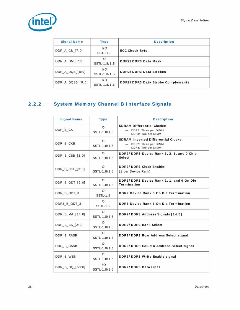
Signal Description
28 Datasheet
2.2.2 System Memory Channel B Interface Signals
DDR_A_CB_[7:0]I/O
SSTL-1.8ECC Check Byte
DDR_A_DM_[7:0]O
SSTL-1.8/1.5DDR2/DDR3 Data Mask
DDR_A_DQS_[8:0]I/O
SSTL-1.8/1.5DDR2/DDR3 Data Strobes
DDR_A_DQSB_[8:0]I/O
SSTL-1.8/1.5DDR2/DDR3 Data Strobe Complements
Signal Name Type Description
DDR_B_CKO
SSTL-1.8/1.5
SDRAM Differential Clocks:— DDR2: Three per DIMM— DDR3: Two per DIMM
DDR_B_CKBO
SSTL-1.8/1.5
SDRAM Inverted Differential Clocks:— DDR2: Three per DIMM— DDR3: Two per DIMM
DDR_B_CSB_[3:0]O
SSTL-1.8/1.5DDR2/DDR3 Device Rank 3, 2, 1, and 0 Chip Select
DDR_B_CKE_[3:0]O
SSTL-1.8/1.5DDR2/DDR3 Clock Enable:(1 per Device Rank)
DDR_B_ODT_[2:0]O
SSTL-1.8/1.5DDR2/DDR3 Device Rank 2, 1, and 0 On Die Termination
DDR_B_ODT_3O
SSTL-1.8DDR2 Device Rank 3 On Die Termination
DDR3_B_ODT_3O
SSTL-1.5DDR3 Device Rank 3 On Die Termination
DDR_B_MA_[14:0]O
SSTL-1.8/1.5DDR2/DDR3 Address Signals [14:0]
DDR_B_BS_[2:0]O
SSTL-1.8/1.5DDR2/DDR3 Bank Select
DDR_B_RASBO
SSTL-1.8/1.5DDR2/DDR3 Row Address Select signal
DDR_B_CASBO
SSTL-1.8/1.5DDR2/DDR3 Column Address Select signal
DDR_B_WEBO
SSTL-1.8/1.5DDR2/DDR3 Write Enable signal
DDR_B_DQ_[63:0]I/O
SSTL-1.8/1.5DDR2/DDR3 Data Lines
Signal Name Type Description

Datasheet 29
Signal Description
2.2.3 System Memory Miscellaneous Signals
DDR_B_CB_[7:0]I/O
SSTL-1.8ECC Check Byte
DDR_B_DM_[7:0]O
SSTL-1.8/1.5DDR2/DDR3 Data Mask
DDR_B_DQS_[8:0]I/O
SSTL-1.8/1.5DDR2/DDR3 Data Strobes
DDR_B_DQSB_[8:0]
I/OSSTL-1.8/1.5
DDR2/DDR3 Data Strobe Complements
Signal Name Type Description
DDR_RCOMPXPDI/OA
System Memory Pull-down RCOMP
DDR_RCOMPXPUI/OA
System Memory Pull-up RCOMP
DDR_RCOMPYPDI/OA
System Memory Pull-down RCOMP
DDR_RCOMPYPUI/OA
System Memory Pull-up RCOMP
DDR_VREFIA
System Memory Reference Voltage
DDR_RCOMPVOHIA
System Memory Pull-up Reference Signal
DDR_RCOMPVOLIA
System Memory Pull-down Reference Signal
DDR3_DRAM_PWROKIA
DDR3 VCC_DDR Power OK
DDR3_DRAMRSTBO
SSTL-1.5DDR3 Reset Signal
Signal Name Type Description

Signal Description
30 Datasheet
2.3 PCI Express* Interface Signals
2.4 Controller Link Interface Signals
Signal Name Type Description
PEG_RXN_[15:0]PEG_RXP_[15:0]
I/OPCIE
Primary PCI Express Receive Differential PairThe MCH supports a maximum width of x16 where all lanes are used.
PEG_TXN_[15:0]PEG_TXP_[15:0]
OPCIE
Primary PCI Express Transmit Differential PairThe MCH supports a maximum width of x16 where all lanes are used.
PEG2_RXN_[15:0]PEG2_RXP_[15:0]
I/OPCIE
Secondary PCI Express Receive Differential Pair. The MCH supports a maximum width of x16 where all lanes are used.
PEG2_TXN_[15:0]PEG2_TXP_[15:0]
OPCIE
Secondary PCI Express Transmit Differential Pair. The MCH supports a maximum width of x16 where all lanes are used.
EXP_COMPOIA
Primary PCI Express Output Current Compensation
EXP_COMPII
APrimary PCI Express Input Current Compensation
EXP2_COMPOIA
Secondary PCI Express Output Current Compensation
EXP2_COMPIIA
Secondary PCI Express Input Current Compensation
Signal Name Type Description
CL_DATAI/O
CMOSController Link Data (Bi-directional)
CL_CLKI/O
CMOSController Link Clock (Bi-directional)
CL_VREFI
CMOSController Link VREF
CL_RST#I
CMOSController Link Reset (Active low)

Datasheet 31
Signal Description
2.5 Clocks, Reset, and Miscellaneous
Signal Name Type Description
HPL_CLKINPHPL_CLKINN
ICMOS
Differential Host Clock In: These pins receive a differential host clock from the external clock synthesizer. This clock is used by all of the MCH logic that is in the Host clock domain.
EXP_CLKINPEXP_CLKINN
ICMOS
Differential Primary PCI Express Clock In: These pins receive a differential 100 MHZ Serial Reference clock from the external clock synthesizer. This clock is used to generate the clocks necessary for the support of Primary PCI Express and DMI.
EXP2_CLKINPEXP2_CLKINN
ICMOS
Differential Secondary PCI Express Clock In: These pins receive a differential 100 MHZ Serial Reference clock from the external clock synthesizer. This clock is used to generate the clocks necessary for the support of Secondary PCI Express.
RSTINBI
SSTL
Reset In: When asserted this signal will asynchronously reset the MCH logic. This signal is connected to the PCIRST# output of the ICH. All PCI Express output signals and DMI output signals will also tri-state compliant to PCI Express Rev 2.0 specification.
This input should have a Schmitt trigger to avoid spurious resets.This signal is required to be 3.3 V tolerant.
CL_PWROKI/O
SSTL
CL Power OK: When asserted, CL_PWROK is an indication to the MCH that core power (VCC_CL) has been stable for at least 10 us.
EXP_SLRI
CMOS
PCI Express* Static Lane Reversal/Form Factor Selection: MCH’s PCI Express lane numbers are reversed to differentiate BTX and ATX form factors0 = MCH PCI Express lane numbers are reversed (BTX)1 = Normal operation (ATX)
BSEL[2:0]I
CMOS
Bus Speed Select: At the deassertion of PWROK, the value sampled on these pins determines the expected frequency of the bus.
MTYPEI
GTL+
Memory Type: Determines DDR2 or DDR3 board0 = DDR31 = DDR2
PWROKI/O
SSTLPower OK: When asserted, PWROK is an indication to the MCH that core power has been stable for at least 10 us.
ICH_SYNCBO
HVCMOSICH Sync: This signal synchronizes the MCH with the ICH.
ALLZTESTI
GTL+All Z Test: This signal is used for chipset Bed of Nails testing to execute All Z Test. It is used as output for XOR Chain testing.
XORTESTI
GTL+XOR Chain Test: This signal is used for chipset Bed of Nails testing to execute XOR Chain Test.
TEST[3:0]I/OA
In Circuit Test: These pins should be connected to test points on the motherboard. They are internally shorted to the package ground and can be used to determine if the corner balls on the MCH are correctly soldered down to the motherboard. These pins should NOT connect to ground on the motherboard. If TEST[3:0] are not going to be used, they should be left as no connects.

Signal Description
32 Datasheet
2.6 Direct Media Interface
2.7 Power and Grounds
§ §
Signal Name Type Description
DMI_RXP_[3:0]DMI_RXN_[3:0]
IDMI
Direct Media Interface: Receive differential pair (RX). MCH-ICH serial interface input
DMI_TXP_[3:0]DMI_TXN_[3:0]
ODMI
Direct Media Interface: Transmit differential pair (TX). MCH-ICH serial interface output
Name Voltage Description
VCC 1.25 V Core Power
VTT 1.1 V/1.2 V Processor System Bus Power
VCC_EXP 1.25 V PCI Express* and DMI Power
VCC_DDR 1.8 V/1.5V DDR2/DDR3 System Memory Power
VCC_CKDDR 1.8V/1.5V DDR2/DDR3 System Clock Memory Power
VCC3_3 3.3 V 3.3 V CMOS Power
VCCAPLL_EXP 1.25 V Primary PCI Express PLL Analog Power
VCCAPLL_EXP2 1.25 V Secondary PCI Express PLL Analog Power
VCCA_hplL 1.25 V Host PLL Analog Power
VCCA_mpl 1.25 V System Memory PLL Analog Power
VCCABG_EXP 3.3 V PCI Express* Analog Power
VCC_CL 1.25 V Controller Link Aux Power
VSS 0 V Ground

Datasheet 33
System Address Map
3 System Address Map
The MCH supports 64 GB (36 bit) of host address space and 64 KB+3 of addressable I/O space. There is a programmable memory address space under the 1 MB region which is divided into regions which can be individually controlled with programmable attributes such as Disable, Read/Write, Write Only, or Read Only. Attribute programming is described in the Register Description section. This section focuses on how the memory space is partitioned and what the separate memory regions are used for. I/O address space has simpler mapping and is explained near the end of this section.
The MCH supports PCI Express* upper pre-fetchable base/limit registers. This allows the PCI Express unit to claim IO accesses above 36 bit, complying with the PCI Express Specification. Addressing of greater than 8 GB is allowed on either the DMI Interface or PCI Express interface. The MCH supports a maximum of 8 GB of DRAM. No DRAM memory will be accessible above 8 GB.
In the following sections, it is assumed that all of the compatibility memory ranges reside on the DMI Interface. The MCH does not remap APIC or any other memory spaces above TOLUD (Top of Low Usable DRAM). The TOLUD register is set to the appropriate value by BIOS. The reclaim base/reclaim limit registers remap logical accesses bound for addresses above 4 GB onto physical addresses that fall within DRAM.
The Address Map includes a number of programmable ranges:
• Device 0
— PXPEPBAR – Egress port registers. Necessary for setting up VC1 as an isochronous channel using time based weighted round robin arbitration. (4 KB window)
— MCHBAR – Memory mapped range for internal MCH registers. For example, memory buffer register controls. (16 KB window)
— PCIEXBAR – Flat memory-mapped address spaced to access device configuration registers. This mechanism can be used to access PCI configuration space (0–FFh) and Extended configuration space (100h–FFFh) for PCI Express devices. This enhanced configuration access mechanism is defined in the PCI Express specification. (64 MB, 128 MB, or 256 MB window).
— DMIBAR –This window is used to access registers associated with the Direct Media Interface (DMI) register memory range. (4 KB window)
• Device 1
— MBASE1/MLIMIT1 – PCI Express port non-prefetchable memory access window.
— PMBASE1/PMLIMIT1 – PCI Express port prefetchable memory access window.
— PMUBASE/PMULIMIT – PCI Express port upper prefetchable memory access window
— IOBASE1/IOLIMIT1 – PCI Express port I/O access window.

System Address Map
34 Datasheet
• Device 3
— ME Control
• Device 6, Function 0
— MBASE1/MLIMIT1 – PCI Express port non-prefetchable memory access window.
— PMBASE1/PMLIMIT1 – PCI Express port prefetchable memory access window.
— PMUBASE/PMULIMIT – PCI Express port upper prefetchable memory access window
— IOBASE1/IOLIMIT1 – PCI Express port I/O access window.
The rules for the above programmable ranges are:
1. ALL of these ranges MUST be unique and NON-OVERLAPPING. It is the BIOS or system designers' responsibility to limit memory population so that adequate PCI, PCI Express, High BIOS, and PCI Express Memory Mapped space, and APIC memory space can be allocated.
2. In the case of overlapping ranges with memory, the memory decode will be given priority. This is an Intel Trusted Execution Technology requirement. It is necessary to get Intel TET protection checks, avoiding potential attacks.
3. There are NO Hardware Interlocks to prevent problems in the case of overlapping ranges.
4. Accesses to overlapped ranges may produce indeterminate results.
5. The only peer-to-peer cycles allowed below the top of Low Usable memory (register TOLUD) are DMI Interface to PCI Express range writes.
Figure 2 represents system memory address map in a simplified form.

Datasheet 35
System Address Map
NOTE: Do not follow the EP UMA requirement.
Figure 2. System Address Ranges
Mai
n M
emor
y Ad
dres
s Ra
nge
Mai
n M
emor
y Ad
dres
s Ra
nge
4G
Mai
n M
emor
y Re
clai
m
Addr
ess
Rang
e
64G
RECL
AIM
BAS
E
RECL
AIM
LIM
IT =
RECL
AIM
BAS
E + x
OS
VISI
BLE
< 4 GB
PCI
Mem
ory
Addr
ess
Rang
e (s
ubtra
ctiv
ely
deco
ded
to
DMI)
OS
INVI
SIBL
E RE
CLAI
M
OS
VISI
BLE
> 4 GB
ST
OLE
N ( 0 - 2
56 M
B )
EP - UM
A ( 1 - 6
4 MB )
TOM
HOST
/SYS
TEM
VIE
WPH
YSIC
AL M
EMO
RY
(DRA
M C
ONT
ROLL
ER V
IEW
)
TSEG
TSEG
( 0 - 8
MB )
X
00
PCI
Mem
ory
Addr
ess
Rang
e (s
ubtra
ctiv
ely
deco
ded
to
DMI)
TSEG
BAS
E
EP S
tole
n BA
SE
1 MB a
ligne
d
1 MB a
ligne
d
64 MB
alig
ned
1 MB a
ligne
d
64M
B al
igne
d
64M
B al
igne
d
64 MB
alig
ned
for r
ecla
im
0 MB - 63
MB W
aste
d 64 MB
alig
ned
TOLU
D BA
SE64
MB
alig
ned
TOUU
D BA
SE
Lega
cy
Addr
ess
Rang
e
1MB
Inde
pend
ently
Pro
gram
mab
le No
n - Overla
ppin
g W
indo
ws
Devi
ce 0
Bars
( PXPEP
BAR ,
MCH
BAR ,
PCIE
XBAR ,
DMIB
AR )
Devi
ce 1
Bars
( MBASE 1 /
MLI
MIT 1 ,
PMBA
SE 1 /
PMLI
MIT 1 )
Devi
ce0
(Sto
len
Mem
ory )
Devi
ce 3
( EPHEC
IBAR ,
EPHE
CI 2 BAR
, E
PKTB
AR )
Inde
pend
ently
Pro
gram
mab
le No
n - Overla
ppin
g W
indo
ws
Devi
ce 0
Bars
( PXPEP
BAR ,
MCH
BAR ,
PCIE
XBAR ,
DMIB
AR )
Devi
ce 1
Bars
( PMUBA
SE 1 /
PMUL
IMIT 1 )
Devi
ce 3
( EPHEC
IBAR ,
EPHE
CI 2 BAR
)
MC HBA
R ( GFX
VTBA
R , DM
IVC 1 BAR
, VT
MEB
AR ,
VTDP
VC 0 BAR
)
Stol
en B
ASE
Devi
ce 6
Bars
( MBASE 1 /
MLI
MIT 1 ,
PMBA
SE 1 /
PMLI
MIT 1 )

System Address Map
36 Datasheet
3.1 Legacy Address Range
This area is divided into the following address regions:
• 0 - 640 KB – DOS Area
• 640 - 768 KB – Legacy Video Buffer Area
• 768 - 896 KB in 16 KB sections (total of 8 sections) – Expansion Area
• 896 -960 KB in 16 KB sections (total of 4 sections) – Extended System BIOS Area
• 960 KB - 1 MB Memory – System BIOS Area
3.1.1 DOS Range (0h – 9_FFFFh)
The DOS area is 640 KB (0000_0000h – 0009_FFFFh) in size and is always mapped to the main memory controlled by the MCH.
Figure 3. DOS Legacy Address Range
Expansion Area128 KB (16 KB x 8)
000C_0000h
000D_FFFFh896 KB
Extended System BIOS (Lower) 64 KB (16 KB x 4)000E_0000h
000E_FFFFh960 KB
Legacy Video Area(SMM Memory)
128 KB000A_0000h
000B_FFFFh768 KB
DOS Area
0000_0000h
0009_FFFFh640 KB
System BIOS (Upper)64 KB000F_0000h
000F_FFFFh1 MB
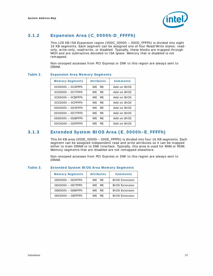
Datasheet 37
System Address Map
3.1.2 Expansion Area (C_0000h-D_FFFFh)
This 128 KB ISA Expansion region (000C_0000h – 000D_FFFFh) is divided into eight 16 KB segments. Each segment can be assigned one of four Read/Write states: read-only, write-only, read/write, or disabled. Typically, these blocks are mapped through MCH and are subtractive decoded to ISA space. Memory that is disabled is not remapped.
Non-snooped accesses from PCI Express or DMI to this region are always sent to DRAM.
3.1.3 Extended System BIOS Area (E_0000h–E_FFFFh)
This 64 KB area (000E_0000h – 000E_FFFFh) is divided into four 16 KB segments. Each segment can be assigned independent read and write attributes so it can be mapped either to main DRAM or to DMI Interface. Typically, this area is used for RAM or ROM. Memory segments that are disabled are not remapped elsewhere.
Non-snooped accesses from PCI Express or DMI to this region are always sent to DRAM.
Table 2. Expansion Area Memory Segments
Memory Segments Attributes Comments
0C0000h – 0C3FFFh WE RE Add-on BIOS
0C4000h – 0C7FFFh WE RE Add-on BIOS
0C8000h – 0CBFFFh WE RE Add-on BIOS
0CC000h – 0CFFFFh WE RE Add-on BIOS
0D0000h – 0D3FFFh WE RE Add-on BIOS
0D4000h – 0D7FFFh WE RE Add-on BIOS
0D8000h – 0DBFFFh WE RE Add-on BIOS
0DC000h – 0DFFFFh WE RE Add-on BIOS
Table 3. Extended System BIOS Area Memory Segments
Memory Segments Attributes Comments
0E0000h – 0E3FFFh WE RE BIOS Extension
0E4000h – 0E7FFFh WE RE BIOS Extension
0E8000h – 0EBFFFh WE RE BIOS Extension
0EC000h – 0EFFFFh WE RE BIOS Extension

System Address Map
38 Datasheet
3.1.4 System BIOS Area (F_0000h–F_FFFFh)
This area is a single 64 KB segment (000F_0000h – 000F_FFFFh). This segment can be assigned read and write attributes. It is by default (after reset) Read/Write disabled and cycles are forwarded to DMI Interface. By manipulating the Read/Write attributes, the MCH can “shadow” BIOS into the main DRAM. When disabled, this segment is not remapped.
Non-snooped accesses from PCI Express or DMI to this region are always sent to DRAM.
3.1.5 PAM Memory Area Details
The 13 sections from 768 KB to 1 MB comprise what is also known as the PAM Memory Area.
The MCH does not handle IWB (Implicit Write-Back) cycles targeting DMI. Since all memory residing on DMI should be set as non-cacheable, there will normally not be IWB cycles targeting DMI. However, DMI becomes the default target for processor and DMI originated accesses to disabled segments of the PAM region. If the MTRRs covering the PAM regions are set to WB or RD it is possible to get IWB cycles targeting DMI. This may occur for processor originated cycles (in a DP system) and for DMI originated cycles to disabled PAM regions.
For example, say that a particular PAM region is set for “Read Disabled” and the MTRR associated with this region is set to WB. A DMI master generates a memory read targeting the PAM region. A snoop is generated on the FSB and the result is an IWB. Since the PAM region is “Read Disabled” the default target for the Memory Read becomes DMI. The IWB associated with this cycle will cause the MCH to hang.
Non-snooped accesses from PCI Express or DMI to this region are always sent to DRAM.
3.2 Main Memory Address Range (1MB – TOLUD)
This address range extends from 1 MB to the top of Low Usable physical memory that is permitted to be accessible by the MCH (as programmed in the TOLUD register). All accesses to addresses within this range will be forwarded by the MCH to the DRAM unless it falls into the optional TSEG, or optional ISA Hole.
Table 4. System BIOS Area Memory Segments
Memory Segments Attributes Comments
0F0000h – 0FFFFFh WE RE BIOS Area
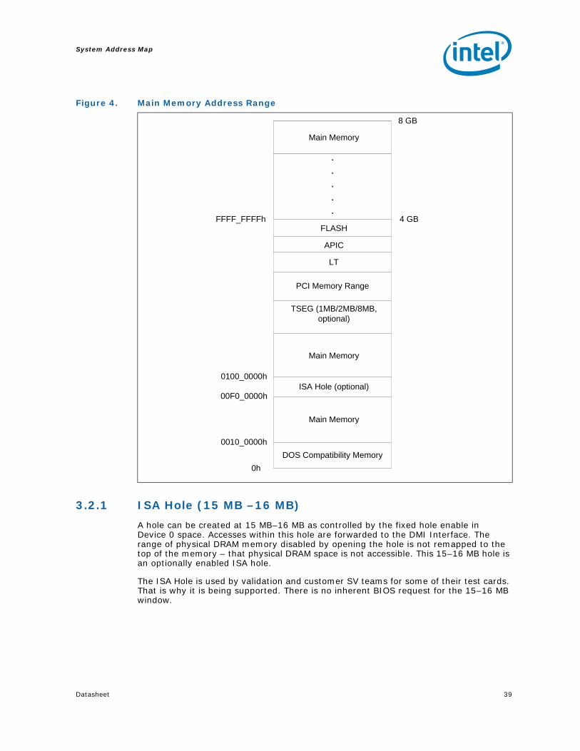
Datasheet 39
System Address Map
3.2.1 ISA Hole (15 MB –16 MB)
A hole can be created at 15 MB–16 MB as controlled by the fixed hole enable in Device 0 space. Accesses within this hole are forwarded to the DMI Interface. The range of physical DRAM memory disabled by opening the hole is not remapped to the top of the memory – that physical DRAM space is not accessible. This 15–16 MB hole is an optionally enabled ISA hole.
The ISA Hole is used by validation and customer SV teams for some of their test cards. That is why it is being supported. There is no inherent BIOS request for the 15–16 MB window.
Figure 4. Main Memory Address Range
DOS Compatibility Memory
Main Memory
ISA Hole (optional)
Main Memory
Main Memory
TSEG (1MB/2MB/8MB, optional)
PCI Memory Range
LT
FLASH
APIC
4 GB
0h
0010_0000h
00F0_0000h
0100_0000h
8 GB
FFFF_FFFFh
.
.
.
.
.

System Address Map
40 Datasheet
3.2.2 TSEG
TSEG is optionally 1 MB, 2 MB, or 8 MB in size. TSEG is below stolen memory, which is at the top of Low Usable physical memory (TOLUD). SMM-mode processor accesses to enabled TSEG access the physical DRAM at the same address. Non-processor originated accesses are not allowed to SMM space. PCI Express, and DMI originated cycles to enabled SMM space are handled as invalid cycle type with reads and writes to location 0 and byte enables turned off for writes. When the extended SMRAM space is enabled, processor accesses to the TSEG range without SMM attribute or without WB attribute are also forwarded to memory as invalid accesses (see table 8). Non-SMM-mode Write Back cycles that target TSEG space are completed to DRAM for cache coherency. When SMM is enabled the maximum amount of memory available to the system is equal to the amount of physical DRAM minus the value in the TSEG register which is fixed at 1 MB, 2 MB, or 8 MB.
3.2.3 Pre-allocated Memory
Voids of physical addresses that are not accessible as general system memory and reside within system memory address range (< TOLUD) are created for SMM-mode, and stolen memory. It is the responsibility of BIOS to properly initialize these regions. The following table details the location and attributes of the regions. Enabling/Disabling these ranges are described in the MCH Control Register Device 0 (GCC).
Figure 5. Pre-allocated Memory Example for 64 MB DRAM, 1 MB stolen and 1 MB TSEG
Memory Segments Attributes Comments
0000_0000h – 03CF_FFFFh R/W Available System Memory 61 MB
03D0_0000h – 03DF_FFFFhSMM Mode Only - processor Reads
TSEG Address Range & Pre-allocated memory

Datasheet 41
System Address Map
3.3 PCI Memory Address Range (TOLUD – 4 GB)
This address range, from the top of low usable DRAM (TOLUD) to 4 GB is normally mapped to the DMI Interface.
Device 0 exceptions are:
• Addresses decoded to the egress port registers (PXPEPBAR)
• Addresses decoded to the memory mapped range for internal MCH registers (MCHBAR)
• Addresses decoded to the flat memory-mapped address spaced to access device configuration registers (PCIEXBAR)
• Addresses decoded to the registers associated with the Direct Media Interface (DMI) register memory range. (DMIBAR)
With PCI Express port, there are two exceptions to this rule.
• Addresses decoded to the PCI Express Memory Window defined by the MBASE1, MLIMIT1, registers are mapped to PCI Express.
• Addresses decoded to the PCI Express prefetchable Memory Window defined by the PMBASE1, PMLIMIT1, registers are mapped to PCI Express.
In an Intel ME configuration, there are exceptions to this rule:
1. Addresses decoded to the ME Keyboard and Text MMIO range (EPKTBAR)
2. Addresses decoded to the ME HECI MMIO range (EPHECIBAR)
3. Addresses decoded to the ME HECI2 MMIO range (EPHECI2BAR)
Some of the MMIO Bars may be mapped to this range or to the range above TOUUD.
There are sub-ranges within the PCI Memory address range defined as APIC Configuration Space, FSB Interrupt Space, and High BIOS Address Range. The exceptions listed above for the PCI Express ports MUST NOT overlap with these ranges.

System Address Map
42 Datasheet
Figure 6. PCI Memory Address Range
DMI Interface(subtractive decode)
FEF0_0000h
4 GB – 2 MB
FSB InterruptsFEE0_0000h
PCI Express Configuration Space
E000_0000h
High BIOSFFE0_0000h
FFFF_FFFFh 4 GB
4 GB – 17 MB
DMI Interface(subtractive decode)FED0_0000h
4 GB – 18 MB
Local (CPU) APICFEC8_0000h
4 GB – 19 MB
I/O APICFEC0_0000h 4 GB – 20 MB
DMI Interface(subtractive decode)
F000_0000h4 GB – 256 MB
Possible address range/size (not
ensured)
4 GB – 512 MB
DMI Interface(subtractive decode)
TOLUD
Optional HSEG FEDA_0000h to FEDB_FFFFh
BARs and PCI Express Port could be
here.

Datasheet 43
System Address Map
3.3.1 APIC Configuration Space (FEC0_0000h–FECF_FFFFh)
This range is reserved for APIC configuration space. The I/O APIC(s) usually reside in the ICH portion of the chipset.
The IOAPIC spaces are used to communicate with IOAPIC interrupt controllers that may be populated in the system. Since it is difficult to relocate an interrupt controller using plug-and-play software, fixed address decode regions have been allocated for them. Processor accesses to the default IOAPIC region (FEC0_0000h to FEC7_FFFFh) are always forwarded to DMI.
The MCH optionally supports additional I/O APICs behind the PCI Express port. When enabled via the PCI Express Configuration register (Device 1 Offset 200h), the PCI Express port will positively decode a subset of the APIC configuration space – specifically FEC8_0000h thru FECF_FFFFh. Memory request to this range would then be forwarded to the PCI Express port. When disabled, any access within entire APIC Configuration space (FEC0_0000h to FECF_FFFFh) is forwarded to DMI.
3.3.2 HSEG (FEDA_0000h–FEDB_FFFFh)
This optional segment from FEDA_0000h to FEDB_FFFFh provides a remapping window to SMM Memory. It is sometimes called the High SMM memory space. SMM-mode processor accesses to the optionally enabled HSEG are remapped to 000A_0000h – 000B_FFFFh. Non-SMM-mode processor accesses to enabled HSEG are considered invalid and are terminated immediately on the FSB. The exceptions to this rule are Non-SMM-mode Write Back cycles which are remapped to SMM space to maintain cache coherency. PCI Express and DMI originated cycles to enabled SMM space are not allowed. Physical DRAM behind the HSEG transaction address is not remapped and is not accessible. All cacheline writes with WB attribute or Implicit write backs to the HSEG range are completed to DRAM like an SMM cycle.
3.3.3 FSB Interrupt Memory Space (FEE0_0000–FEEF_FFFF)
The FSB Interrupt space is the address used to deliver interrupts to the FSB. Any device on PCI Express or DMI may issue a Memory Write to 0FEEx_xxxxh. The MCH will forward this Memory Write along with the data to the FSB as an Interrupt Message Transaction. The MCH terminates the FSB transaction by providing the response and asserting HTRDYB. This Memory Write cycle does not go to DRAM.
3.3.4 High BIOS Area
The top 2 MB (FFE0_0000h – FFFF_FFFFh) of the PCI Memory Address Range is reserved for System BIOS (High BIOS), extended BIOS for PCI devices, and the A20 alias of the system BIOS. The processor begins execution from the High BIOS after reset. This region is mapped to DMI Interface so that the upper subset of this region aliases to 16 MB–256 KB range. The actual address space required for the BIOS is less than 2 MB but the minimum processor MTRR range for this region is 2 MB so that full 2 MB must be considered.

System Address Map
44 Datasheet
3.4 Main Memory Address Space (4 GB to TOUUD)
The MCH supports 36 bit addressing. The maximum main memory size supported is 8 GB total DRAM memory. A hole between TOLUD and 4 GB occurs when main memory size approaches 4 GB or larger. As a result, TOM, and TOUUD registers and RECLAIMBASE/RECLAIMLIMIT registers become relevant.
The new reclaim configuration registers exist to reclaim lost main memory space. The greater than 32 bit reclaim handling will be handled similar to other MCHs.
Upstream read and write accesses above 36-bit addressing will be treated as invalid cycles by PCI Express and DMI.
Top of Memory
The “Top of Memory” (TOM) register reflects the total amount of populated physical memory. This is NOT necessarily the highest main memory address (holes may exist in main memory address map due to addresses allocated for memory-mapped I/O above TOM). TOM is used to allocate the Intel Management Engine's stolen memory. The Intel ME stolen size register reflects the total amount of physical memory stolen by the Intel ME. The ME stolen memory is located at the top of physical memory. The ME stolen memory base is calculated by subtracting the amount of memory stolen by the Intel ME from TOM.
The Top of Upper Usable Dram (TOUUD) register reflects the total amount of addressable DRAM. If reclaim is disabled, TOUUD will reflect TOM minus Intel ME stolen size. If reclaim is enabled, then it will reflect the reclaim limit. Also, the reclaim base will be the same as TOM minus ME stolen memory size to the nearest 64 MB alignment.
TOLUD register is restricted to 4 GB memory (A[31:20]), but the MCH can support up to 16 GB, limited by DRAM pins. For physical memory greater than 4 GB, the TOUUD register helps identify the address range in between the 4 GB boundary and the top of physical memory. This identifies memory that can be directly accessed (including reclaim address calculation) which is useful for memory access indication, early path indication, and trusted read indication. When reclaim is enabled, TOLUD must be 64 MB aligned, but when reclaim is disabled, TOLUD can be 1 MB aligned.
C1DRB3 cannot be used directly to determine the effective size of memory as the values programmed in the DRBs depend on the memory mode (stacked, interleaved). The Reclaim Base/Limit registers also can not be used because reclaim can be disabled. The C0DRB3 register is used for memory channel identification (channel 0 vs. channel 1) in the case of stacked memory.

Datasheet 45
System Address Map
3.4.1 Memory Re-claim Background
The following are examples of Memory Mapped IO devices are typically located below 4 GB:
• High BIOS
• HSEG
• TSEG
• XAPIC
• Local APIC
• FSB Interrupts
• Mbase/Mlimit
• Memory Mapped IO space that supports only 32 B addressing
The MCH provides the capability to re-claim the physical memory overlapped by the Memory Mapped I/O logical address space. The MCH re-maps physical memory from the Top of Low Memory (TOLUD) boundary up to the 4 GB boundary to an equivalent sized logical address range located just below the Intel ME's stolen memory.
3.4.2 Memory Reclaiming
An incoming address (referred to as a logical address) is checked to see if it falls in the memory re-map window. The bottom of the re-map window is defined by the value in the RECLAIMBASE register. The top of the re-map window is defined by the value in the RECLAIMLIMIT register. An address that falls within this window is reclaimed to the physical memory starting at the address defined by the TOLUD register. The TOLUD register must be 64M aligned when RECLAIM is enabled, but can be 1M aligned when reclaim is disabled.
3.5 PCI Express* Configuration Address Space
There is a device 0 register, PCIEXBAR, which defines the base address for the configuration space associated with all devices and functions that are potentially a part of the PCI Express root complex hierarchy. The size of this range will be programmable for the MCH. BIOS must assign this address range such that it will not conflict with any other address ranges.
See the configuration portion of this document for more details.

System Address Map
46 Datasheet
3.6 PCI Express* Address Space
The MCH can be programmed to direct memory accesses to the PCI Express interface when addresses are within either of two ranges specified via registers in MCH’s Device 1 configuration space.
• The first range is controlled via the Memory Base Register (MBASE) and Memory Limit Register (MLIMIT) registers.
• The second range is controlled via the Pre-fetchable Memory Base (PMBASE) and Pre-fetchable Memory Limit (PMLIMIT) registers.
Conceptually, address decoding for each range follows the same basic concept. The top 12 bits of the respective Memory Base and Memory Limit registers correspond to address bits A[31:20] of a memory address . For the purpose of address decoding, the MCH assumes that address bits A[19:0] of the memory base are zero and that address bits A[19:0] of the memory limit address are FFFFFh. This forces each memory address range to be aligned to 1MB boundary and to have a size granularity of 1 MB.
The MCH positively decodes memory accesses to PCI Express memory address space as defined by the following equations:
Memory_Base_Address ≤ Address ≤ Memory_Limit_Address
Prefetchable_Memory_Base_Address ≤ Address ≤ Prefetchable_Memory_Limit_Address
The window size is programmed by the plug-and-play configuration software. The window size depends on the size of memory claimed by the PCI Express device. Normally these ranges will reside above the Top-of-Low Usable-DRAM and below High BIOS and APIC address ranges. They MUST reside above the top of low memory (TOLUD) if they reside below 4 GB and MUST reside above top of upper memory (TOUUD) if they reside above 4 GB or they will steal physical DRAM memory space.
It is essential to support a separate Pre-fetchable range in order to apply USWC attribute (from the processor point of view) to that range. The USWC attribute is used by the processor for write combining.
Note that the MCH Device 1 memory range registers described above are used to allocate memory address space for any PCI Express devices sitting on PCI Express that require such a window.
The PCICMD1 register can override the routing of memory accesses to PCI Express. In other words, the memory access enable bit must be set in the device 1 PCICMD1 register to enable the memory base/limit and pre-fetchable base/limit windows.
For the MCH, the upper PMUBASE1/PMULIMIT1 registers have been implemented for PCI Express Spec compliance. The MCH locates MMIO space above 4 GB using these registers.

Datasheet 47
System Address Map
3.7 System Management Mode (SMM)
System Management Mode uses main memory for System Management RAM (SMM RAM). The MCH supports: Compatible SMRAM (C_SMRAM), High Segment (HSEG), and Top of Memory Segment (TSEG). System Management RAM space provides a memory area that is available for the SMI handlers and code and data storage. This memory resource is normally hidden from the system OS so that the processor has immediate access to this memory space upon entry to SMM. MCH provides three SMRAM options:
• Below 1 MB option that supports compatible SMI handlers.
• Above 1 MB option that allows new SMI handlers to execute with write-back cacheable SMRAM.
• Optional TSEG area of 1 MB, 2 MB, or 8 MB in size. The TSEG area lies below stolen memory.
The above 1 MB solutions require changes to compatible SMRAM handlers code to properly execute above 1 MB.
Note: DMI Interface and PCI Express masters are not allowed to access the SMM space.
3.7.1 SMM Space Definition
SMM space is defined by its addressed SMM space and its DRAM SMM space. The addressed SMM space is defined as the range of bus addresses used by the processor to access SMM space. DRAM SMM space is defined as the range of physical DRAM memory locations containing the SMM code. SMM space can be accessed at one of three transaction address ranges: Compatible, High, and TSEG. The Compatible and TSEG SMM space is not remapped and therefore the addressed and DRAM SMM space is the same address range. Since the High SMM space is remapped the addressed and DRAM SMM space is a different address range. Note that the High DRAM space is the same as the Compatible Transaction Address space. Table 5 describes three unique address ranges.
• Compatible Transaction Address
• High Transaction Address
• TSEG Transaction Address
Table 5. Transaction Address Ranges – Compatible, High, and TSEG
SMM Space Enabled Transaction Address Space DRAM Space (DRAM)
Compatible 000A_0000h to 000B_FFFFh 000A_0000h to 000B_FFFFh
High FEDA_0000h to FEDB_FFFFh 000A_0000h to 000B_FFFFh
TSEG (TOLUD–STOLEN–TSEG) to
TOLUD–STOLEN(TOLUD–STOLEN–TSEG) to
TOLUD–STOLEN
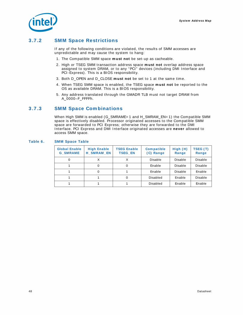
System Address Map
48 Datasheet
3.7.2 SMM Space Restrictions
If any of the following conditions are violated, the results of SMM accesses are unpredictable and may cause the system to hang:
1. The Compatible SMM space must not be set-up as cacheable.
2. High or TSEG SMM transaction address space must not overlap address space assigned to system DRAM, or to any “PCI” devices (including DMI Interface and PCI-Express). This is a BIOS responsibility.
3. Both D_OPEN and D_CLOSE must not be set to 1 at the same time.
4. When TSEG SMM space is enabled, the TSEG space must not be reported to the OS as available DRAM. This is a BIOS responsibility.
5. Any address translated through the GMADR TLB must not target DRAM from A_0000–F_FFFFh.
3.7.3 SMM Space Combinations
When High SMM is enabled (G_SMRAME=1 and H_SMRAM_EN=1) the Compatible SMM space is effectively disabled. Processor originated accesses to the Compatible SMM space are forwarded to PCI Express; otherwise they are forwarded to the DMI Interface. PCI Express and DMI Interface originated accesses are never allowed to access SMM space.
Table 6. SMM Space Table
Global Enable G_SMRAME
High Enable H_SMRAM_EN
TSEG Enable TSEG_EN
Compatible (C) Range
High (H) Range
TSEG (T) Range
0 X X Disable Disable Disable
1 0 0 Enable Disable Disable
1 0 1 Enable Disable Enable
1 1 0 Disabled Enable Disable
1 1 1 Disabled Enable Enable

Datasheet 49
System Address Map
3.7.4 SMM Control Combinations
The G_SMRAME bit provides a global enable for all SMM memory. The D_OPEN bit allows software to write to the SMM ranges without being in SMM mode. BIOS software can use this bit to initialize SMM code at powerup. The D_LCK bit limits the SMM range access to only SMM mode accesses. The D_CLS bit causes SMM (both CSEG and TSEG) data accesses to be forwarded to the DMI Interface or PCI Express. The SMM software can use this bit to write to video memory while running SMM code out of DRAM.
3.7.5 SMM Space Decode and Transaction Handling
Only the processor is allowed to access SMM space. PCI Express and DMI Interface originated transactions are not allowed to SMM space.
3.7.6 Processor WB Transaction to an Enabled SMM Address Space
Processor Writeback transactions (REQa[1]# = 0) to enabled SMM Address Space must be written to the associated SMM DRAM even though D_OPEN=0 and the transaction is not performed in SMM mode. This ensures SMM space cache coherency when cacheable extended SMM space is used.
3.7.7 SMM Access Through TLB
Accesses through TLB address translation to enabled SMM DRAM space are not allowed. Writes will be routed to Memory address 000C_0000h with byte enables de-asserted and reads will be routed to Memory address 000C_0000h. If a TLB translated address hits enabled SMM DRAM space, an error is recorded.
PCI Express and DMI Interface originated accesses are never allowed to access SMM space directly or through the TLB address translation. If a TLB translated address hits enabled SMM DRAM space, an error is recorded.
PCI Express and DMI Interface write accesses through GMADR range will be snooped. Assesses to GMADR linear range (defined via fence registers) are supported. PCI Express and DMI Interface tileY and tileX writes to GMADR are not supported. If, when translated, the resulting physical address is to enabled SMM DRAM space, the request will be remapped to address 000C_0000h with de-asserted byte enables.
Table 7. SMM Control Table
G_SMRAME D_LCK D_CLS D_OPENProcessor
in SMM Mode
SMM Code Access
SMM Data Access
0 x X x x Disable Disable
1 0 X 0 0 Disable Disable
1 0 0 0 1 Enable Enable
1 0 0 1 x Enable Enable
1 0 1 0 1 Enable Disable
1 0 1 1 x Invalid Invalid
1 1 X x 0 Disable Disable
1 1 0 x 1 Enable Enable
1 1 1 x 1 Enable Disable

System Address Map
50 Datasheet
PCI Express and DMI Interface read accesses to the GMADR range are not supported therefore will have no address translation concerns. PCI Express and DMI Interface reads to GMADR will be remapped to address 000C_0000h. The read will complete with UR (unsupported request) completion status.
Fetches are always decoded (at fetch time) to ensure not in SMM (actually, anything above base of TSEG or 640 K–1 M). Thus, they will be invalid and go to address 000C_0000h, but that isn’t specific to PCI Express or DMI; it applies to processor. Also, since the GMADR snoop would not be directly to the SMM space, there wouldn’t be a writeback to SMM. In fact, the writeback would also be invalid (because it uses the same translation) and go to address 000C_0000h.
3.8 Memory Shadowing
Any block of memory that can be designated as read-only or write-only can be “shadowed” into MCH DRAM memory. Typically this is done to allow ROM code to execute more rapidly out of main DRAM. ROM is used as a read-only during the copy process while DRAM at the same time is designated write-only. After copying, the DRAM is designated read-only so that ROM is shadowed. Processor bus transactions are routed accordingly.
3.9 I/O Address Space
The MCH does not support the existence of any other I/O devices beside itself on the processor bus. The MCH generates either DMI Interface or PCI Express bus cycles for all processor I/O accesses that it does not claim. Within the host bridge, the MCH contains two internal registers in the processor I/O space, Configuration Address Register (CONFIG_ADDRESS) and the Configuration Data Register (CONFIG_DATA). These locations are used to implement configuration space access mechanism.
The processor allows 64 K+3 bytes to be addressed within the I/O space. The MCH propagates the processor I/O address without any translation on to the destination bus and therefore provides addressability for 64K+3 byte locations. Note that the upper 3 locations can be accessed only during I/O address wrap-around when processor bus HAB_16 address signal is asserted. HAB_16 is asserted on the processor bus whenever an I/O access is made to 4 bytes from address 0FFFDh, 0FFFEh, or 0FFFFh. HAB_16 is also asserted when an I/O access is made to 2 bytes from address 0FFFFh.
The I/O accesses (other than ones used for configuration space access) are forwarded normally to the DMI Interface bus unless they fall within the PCI Express I/O address range as defined by the mechanisms explained below. I/O writes are NOT posted. Memory writes to ICH or PCI Express are posted. The PCICMD1 register can disable the routing of I/O cycles to the PCI Express.
The MCH responds to I/O cycles initiated on PCI Express or DMI with an UR status. Upstream I/O cycles and configuration cycles should never occur. If one does occur, the request will route as a read to Memory address 000C_0000h so a completion is naturally generated (whether the original request was a read or write). The transaction will complete with an UR completion status.
I/O reads that lie within 8-byte boundaries but cross 4-byte boundaries are issued from the processor as 1 transaction. The MCH will break this into 2 separate transactions. I/O writes that lie within 8-byte boundaries but cross 4-byte boundaries are assumed to be split into 2 transactions by the processor.

Datasheet 51
System Address Map
3.9.1 PCI Express* I/O Address Mapping
The MCH can be programmed to direct non-memory (I/O) accesses to the PCI Express bus interface when processor initiated I/O cycle addresses are within the PCI Express I/O address range. This range is controlled via the I/O Base Address (IOBASE) and I/O Limit Address (IOLIMIT) registers in MCH Device 1 configuration space.
Address decoding for this range is based on the following concept. The top 4 bits of the respective I/O Base and I/O Limit registers correspond to address bits A[15:12] of an I/O address. For the purpose of address decoding, the MCH assumes that lower 12 address bits A[11:0] of the I/O base are zero and that address bits A[11:0] of the I/O limit address are FFFh. This forces the I/O address range alignment to 4 KB boundary and produces a size granularity of 4 KB.
The MCH positively decodes I/O accesses to PCI Express I/O address space as defined by the following equation:
I/O_Base_Address ≤ Processor I/O Cycle Address ≤ I/O_Limit_Address
The effective size of the range is programmed by the plug-and-play configuration software and it depends on the size of I/O space claimed by the PCI Express device.
Note that the MCH Device 1 and/or Device 6 I/O address range registers defined above are used for all I/O space allocation for any devices requiring such a window on PCI Express.
The PCICMD1 register can disable the routing of I/O cycles to PCI Express.
§ §

System Address Map
52 Datasheet

Datasheet 53
MCH Register Description
4 MCH Register Description
The MCH contains two sets of software accessible registers, accessed via the Host processor I/O address space: Control registers and internal configuration registers.
• Control registers are I/O mapped into the processor I/O space, which control access to PCI and PCI Express configuration space (see Chapter 6).
• Internal configuration registers residing within the MCH are partitioned into two logical device register sets (“logical” since they reside within a single physical device). The first register set is dedicated to Host Bridge functionality (i.e., DRAM configuration, other chipset operating parameters and optional features). The second register block is dedicated to Host-to-PCI Express Bridge functions (controls PCI Express interface configurations and operating parameters).
The MCH internal registers (I/O Mapped, Configuration and PCI Express Extended Configuration registers) are accessible by the processor. The registers that reside within the lower 256 bytes of each device can be accessed as Byte, Word (16-bit), or DWord (32-bit) quantities, with the exception of CONFIG_ADDRESS, which can only be accessed as a DWord. All multi-byte numeric fields use “little-endian” ordering (i.e., lower addresses contain the least significant parts of the field). Registers that reside in bytes 256 through 4095 of each device may only be accessed using memory-mapped transactions in DWord (32-bit) quantities.
Some of the MCH registers described in this section contain reserved bits. These bits are labeled “Reserved”. Software must deal correctly with fields that are reserved. On reads, software must use appropriate masks to extract the defined bits and not rely on reserved bits being any particular value. On writes, software must ensure that the values of reserved bit positions are preserved. That is, the values of reserved bit positions must first be read, merged with the new values for other bit positions and then written back. Note the software does not need to perform read, merge, and write operation for the Configuration Address Register.
In addition to reserved bits within a register, the MCH contains address locations in the configuration space of the Host Bridge entity that are marked either “Reserved” or “Intel Reserved”. The MCH responds to accesses to “Reserved” address locations by completing the host cycle. When a “Reserved” register location is read, a zero value is returned. (“Reserved” registers can be 8-, 16-, or 32-bits in size). Writes to “Reserved” registers have no effect on the MCH. Registers that are marked as “Intel Reserved” must not be modified by system software. Writes to “Intel Reserved” registers may cause system failure. Reads from “Intel Reserved” registers may return a non-zero value.
Upon a Full Reset, the MCH sets its entire set of internal configuration registers to predetermined default states. Some register values at reset are determined by external strapping options. The default state represents the minimum functionality feature set required to successfully bringing up the system. Hence, it does not represent the optimal system configuration. It is the responsibility of the system initialization software (usually BIOS) to properly determine the DRAM configurations, operating parameters and optional system features that are applicable, and to program the MCH registers accordingly.

MCH Register Description
54 Datasheet
4.1 Register TerminologyThe following table shows the register-related terminology that is used.
Item Description
RO Read Only bit(s). Writes to these bits have no effect.
RO/S Read Only / Sticky. Writes to these bits have no effect. These are status bits only. Bits are not returned to their default values by “warm” reset, but will be reset with a cold/complete reset (for PCI Express related bits, a cold reset is “Power Good Reset” as defined in the PCI Express specification).
RS/WC Read Set / Write Clear bit(s). These bits are set to ‘1’ when read and then will continue to remain set until written. A write of ‘1’ clears (sets to ‘0’) the corresponding bit(s) and a write of ‘0’ has no effect.
R/W Read / Write bit(s). These bits can be read and written.
R/WC Read / Write Clear bit(s). These bits can be read. Internal events may set this bit. A write of ‘1’ clears (sets to ‘0’) the corresponding bit(s) and a write of ‘0’ has no effect.
R/WC/S Read / Write Clear / Sticky bit(s). These bits can be read. Internal events may set this bit. A write of ‘1’ clears (sets to ‘0’) the corresponding bit(s) and a write of ‘0’ has no effect. Bits are not cleared by "warm" reset, but will be reset with a cold/complete reset (for PCI Express related bits a cold reset is “Power Good Reset” as defined in the PCI Express Specification).
R/W/L Read / Write / Lockable bit(s). These bits can be read and written. Additionally, there is a bit (which may or may not be a bit marked R/W/L) that, when set, prohibits this bit field from being writeable (bit field becomes Read Only).
R/W/K Read / Write / Key bit(s). These bits can be read and written by software. Additionally this bit when set, prohibits some other bit field(s) from being writeable (bit fields become Read Only).
R/W/L Read / Write / Lockable bit(s). These bits can be read and written. Additionally there is a bit (which may or may not be a bit marked R/W/L) that, when set, prohibits this bit field from being writeable (bit field becomes Read Only).
R/W/S Read / Write / Sticky bit(s). These bits can be read and written. Bits are not cleared by "warm" reset, but will be reset with a cold/complete reset (for PCI Express related bits a cold reset is “Power Good Reset” as defined in the PCI Express Specification).
R/WSC Read / Write Self Clear bit(s). These bits can be read and written. When the bit is ‘1’, hardware may clear the bit to ‘0’ based upon internal events, possibly sooner than any subsequent read could retrieve a ‘1’.
R/WSC/L Read / Write Self Clear / Lockable bit(s). These bits can be read and written. When the bit is ‘1’, hardware may clear the bit to ‘0’ based upon internal events, possibly sooner than any subsequent read could retrieve a ‘1’. Additionally there is a bit (which may or may not be a bit marked R/W/L) that, when set, prohibits this bit field from being writeable (bit field becomes Read Only).
R/WO Write Once bit(s). Once written, bits with this attribute become Read Only. These bits can only be cleared by a Reset.
W Write Only. Whose bits may be written, but will always-return zeros when read. They are used for write side effects. Any data written to these registers cannot be retrieved.

Datasheet 55
MCH Register Description
4.2 Configuration Process and Registers
4.2.1 Platform Configuration Structure
The DMI physically connects the MCH and the Intel ICH9; thus, from a configuration standpoint, the DMI is logically PCI bus 0. As a result, all devices internal to the MCH and the ICH appear to be on PCI bus 0.
Note: The ICH9 internal LAN controller does not appear on bus 0 – it appears on the external PCI bus and this number is configurable.
The system’s primary PCI expansion bus is physically attached to the ICH and from a configuration perspective, appears to be a hierarchical PCI bus behind a PCI-to-PCI bridge; therefore, it has a programmable PCI Bus number. The PCI Express interface appears to system software to be a real PCI bus behind a PCI-to-PCI bridge that is a device resident on PCI bus 0.
Note: A physical PCI bus 0 does not exist; DMI and the internal devices in the MCH and ICH logically constitute PCI Bus 0 to configuration software (see Figure 7).
Figure 7. Conceptual Platform PCI Configuration Diagram
CPU
PCI Configuration Window in I/O Space
Manageability Engine Device
Bus 0 Device 3
Bus 0
Direct Media Interface
DRAM Controller Interface Device
Bus 0 Device 0
MCH
Secondary Host-PCI Express Bridge
Bus 0 Device 6
Primary Host-PCI Express Bridge Bus 0 Device 1
MCH Register Description
56 Datasheet
The MCH contains four PCI devices within a single physical component. The configuration registers for the four devices are mapped as devices residing on PCI bus 0.
• Device 0: Host Bridge/DRAM Controller. Logically this appears as a PCI device residing on PCI bus 0. Device 0 contains the standard PCI header registers, PCI Express base address register, DRAM control (including thermal/throttling control), and configuration for the DMI and other MCH specific registers.
• Device 1: Primary Host-PCI Express Bridge. Logically this appears as a “virtual” PCI-to-PCI bridge residing on PCI bus 0 and is compliant with PCI Express Specification Rev 1.0. Device 1 contains the standard PCI-to-PCI bridge registers and the standard PCI Express/PCI configuration registers (including the PCI Express memory address mapping). It also contains Isochronous and Virtual Channel controls in the PCI Express extended configuration space.
• Device 3: Manageability Engine Device. Logically, this appears as a PCI device residing on PCI bus 0. Physically, device 3.
• Device 6: Secondary Host-PCI Express Bridge. Logically this appears as a “virtual” PCI-to-PCI bridge residing on PCI bus 0 and is compliant with PCI Express Specification Rev 1.0. Device 6 contains the standard PCI-to-PCI bridge registers and the standard PCI Express/PCI configuration registers (including the PCI Express memory address mapping). It also contains Isochronous and Virtual Channel controls in the PCI Express extended configuration space.
4.3 Configuration MechanismsThe processor is the originator of configuration cycles so the FSB is the only interface in the platform where these mechanisms are used. The MCH translates transactions received through both configuration mechanisms to the same format.
4.3.1 Standard PCI Configuration Mechanism
The following is the mechanism for translating processor I/O bus cycles to configuration cycles.
The PCI specification defines a slot based "configuration space" that allows each device to contain up to 8 functions with each function containing up to 256 8-bit configuration registers. The PCI specification defines two bus cycles to access the PCI configuration space: Configuration Read and Configuration Write. Memory and I/O spaces are supported directly by the processor. Configuration space is supported by a mapping mechanism implemented within the MCH.
The configuration access mechanism makes use of the CONFIG_ADDRESS Register (at I/O address 0CF8h though 0CFBh) and CONFIG_DATA Register (at I/O address 0CFCh though 0CFFh). To reference a configuration register a DW I/O write cycle is used to place a value into CONFIG_ADDRESS that specifies the PCI bus, the device on that bus, the function within the device and a specific configuration register of the device function being accessed. CONFIG_ADDRESS[31] must be 1 to enable a configuration cycle. CONFIG_DATA then becomes a window into the four bytes of configuration space specified by the contents of CONFIG_ADDRESS. Any read or write to CONFIG_DATA will result in the MCH translating the CONFIG_ADDRESS into the appropriate configuration cycle.

Datasheet 57
MCH Register Description
The MCH is responsible for translating and routing the processor’s I/O accesses to the CONFIG_ADDRESS and CONFIG_DATA registers to internal MCH configuration registers, DMI or PCI Express.
4.3.2 PCI Express Enhanced Configuration Mechanism
PCI Express extends the configuration space to 4096 bytes per device/function as compared to 256 bytes allowed by PCI Specification Revision 2.3. PCI Express configuration space is divided into a PCI 2.3 compatible region, which consists of the first 256B of a logical device’s configuration space and a PCI Express extended region, which consists of the remaining configuration space.
The PCI compatible region can be accessed using either the Standard PCI Configuration Mechanism or using the PCI Express Enhanced Configuration Mechanism described in this section. The extended configuration registers may only be accessed using the PCI Express Enhanced Configuration Mechanism. To maintain compatibility with PCI configuration addressing mechanisms, system software must access the extended configuration space using 32-bit operations (32-bit aligned) only. These 32-bit operations include byte enables allowing only appropriate bytes within the DWord to be accessed. Locked transactions to the PCI Express memory mapped configuration address space are not supported. All changes made using either access mechanism are equivalent.
The PCI Express Enhanced Configuration Mechanism utilizes a flat memory-mapped address space to access device configuration registers. This address space is reported by the system firmware to the operating system. There is a register, PCIEXBAR, that defines the base address for the block of addresses below 4 GB for the configuration space associated with busses, devices and functions that are potentially a part of the PCI Express root complex hierarchy. In the PCIEXBAR register there exists controls to limit the size of this reserved memory mapped space. 256 MB is the amount of address space required to reserve space for every bus, device, and function that could possibly exist. Options for 128 MB and 64 MB exist in order to free up those addresses for other uses. In these cases the number of busses and all of their associated devices and functions are limited to 128 or 64 busses respectively.
The PCI Express Configuration Transaction Header includes an additional 4 bits (ExtendedRegisterAddress[3:0]) between the Function Number and Register Address fields to provide indexing into the 4 KB of configuration space allocated to each potential device. For PCI Compatible Configuration Requests, the Extended Register Address field must be all zeros.

MCH Register Description
58 Datasheet
As with PCI devices, each device is selected based on decoded address information that is provided as a part of the address portion of Configuration Request packets. A PCI Express device will decode all address information fields (bus, device, function and extended address numbers) to provide access to the correct register.
To access this space (steps 1, 2, 3 are done only once by BIOS),
1. Use the PCI compatible configuration mechanism to enable the PCI Express enhanced configuration mechanism by writing 1 to bit 0 of the PCIEXBAR register.
2. Use the PCI compatible configuration mechanism to write an appropriate PCI Express base address into the PCIEXBAR register.
3. Calculate the host address of the register you wish to set using (PCI Express base + (bus number * 1 MB) + (device number * 32KB) + (function number * 4 KB) + (1 B * offset within the function) = host address).
4. Use a memory write or memory read cycle to the calculated host address to write or read that register.
4.4 Routing Configuration AccessesThe MCH supports two PCI related interfaces: DMI and PCI Express. The MCH is responsible for routing PCI and PCI Express configuration cycles to the appropriate device that is an integrated part of the MCH or to one of these two interfaces. Configuration cycles to the ICH internal devices and Primary PCI (including downstream devices) are routed to the ICH via DMI. Configuration cycles to the PCI Express PCI compatibility configuration space are routed to the PCI Express port device or associated link.
Figure 8. Memory Map to PCI Express Device Configuration Space
MemMap PCIExpress
Bus 255
FFFFFFFh
Bus 1
Bus 0
1FFFFFh
FFFFFh
0h
Device 31
FFFFFh
Device 1
Device 0
FFFFh
7FFFh
Function 7
7FFFh
Function 1
Function 0
1FFFh
FFFh
FFFh
PCI Compatible
Config Space
PCI Compatible
Config Header
FFh
3Fh
PCI Express* Extended
Configuration Space
Located By PCI Express* Base
Address

Datasheet 59
MCH Register Description
4.4.1 Internal Device Configuration Accesses
The MCH decodes the Bus Number (bits 23:16) and the Device Number fields of the CONFIG_ADDRESS register. If the Bus Number field of CONFIG_ADDRESS is 0 the configuration cycle is targeting a PCI Bus #0 device.
If the targeted PCI Bus 0 device exists in the MCH and is not disabled, the configuration cycle is claimed by the appropriate device.
Figure 9. MCH Configuration Cycle Flow Chart
DW I/O Write toCONFIG_ADDRESS
with bit 31 = 1
I/O Read/Write toCONFIG_DATA
MCH Generates Type 1 Access to PCI Express
MCH allows cycle to go to DMI resulting in Master Abort
Bus# > SEC BUSBus# ≤ SUB BUS
in MCH Dev 1
Bus# = 0
Device# = 1 &Dev # 1 Enabled& Function# = 0
Device# = 0 &Function# = 0
MCH GeneratesDMI Type 1
Configuration Cycle
Bus# =SECONDARYBUS
in MCH Dev 1
MCH Claims
MCH Claims
Yes
No
Yes
Yes
No
No
Yes
Yes
No
No
Device# = 0 MCH GeneratesType 0 Accessto PCI Express
Yes
MCH GeneratesDMI Type 0
Configuration Cycle
No
MCH Register Description
60 Datasheet
4.4.2 Bridge Related Configuration Accesses
Configuration accesses on PCI Express or DMI are PCI Express Configuration TLPs (Transaction Layer Packets):
• Bus Number [7:0] is Header Byte 8 [7:0]• Device Number [4:0] is Header Byte 9 [7:3]• Function Number [2:0] is Header Byte 9 [2:0]
And special fields for this type of TLP:
• Extended Register Number [3:0] is Header Byte 10 [3:0]• Register Number [5:0] is Header Byte 11 [7:2]
See the PCI Express specification for more information on both the PCI 2.3 compatible and PCI Express Enhanced Configuration Mechanism and transaction rules.
4.4.2.1 PCI Express Configuration Accesses
When the Bus Number of a type 1 Standard PCI Configuration cycle or PCI Express Enhanced Configuration access matches the Device 1 Secondary Bus Number a PCI Express Type 0 Configuration TLP is generated on the PCI Express link targeting the device directly on the opposite side of the link. This should be Device 0 on the bus number assigned to the PCI Express link (likely Bus 1).
The device on other side of link must be Device 0. The MCH will Master Abort any Type 0 Configuration access to a non-zero Device number. If there is to be more than one device on that side of the link there must be a bridge implemented in the downstream device.
When the Bus Number of a type 1 Standard PCI Configuration cycle or PCI Express Enhanced Configuration access is within the claimed range (between the upper bound of the bridge device’s Subordinate Bus Number register and the lower bound of the bridge device’s Secondary Bus Number register) but does not match the Device 1 Secondary Bus Number, a PCI Express Type 1 Configuration TLP is generated on the secondary side of the PCI Express link.
PCI Express Configuration Writes:
• Internally the host interface unit will translate writes to PCI Express extended configuration space to configuration writes on the backbone.
• Writes to extended space are posted on the FSB, but non-posted on the PCI Express or DMI (i.e., translated to config writes)
4.4.2.2 DMI Configuration Accesses
Accesses to disabled MCH internal devices, bus numbers not claimed by the Host-PCI Express bridge, or PCI Bus #0 devices not part of the MCH will subtractively decode to the ICH and consequently be forwarded over the DMI via a PCI Express configuration TLP.
If the Bus Number is zero, the MCH will generate a Type 0 Configuration Cycle TLP on DMI. If the Bus Number is non-zero, and falls outside the range claimed by the Host-PCI Express bridge, the MCH will generate a Type 1 Configuration Cycle TLP on DMI.
The ICH routes configurations accesses in a manner similar to the MCH. The ICH decodes the configuration TLP and generates a corresponding configuration access. Accesses targeting a device on PCI Bus #0 may be claimed by an internal device. The ICH compares the non-zero Bus Number with the Secondary Bus Number and

Datasheet 61
MCH Register Description
Subordinate Bus Number registers of its PCI-to-PCI bridges to determine if the configuration access is meant for Primary PCI, or some other downstream PCI bus or PCI Express link.
Configuration accesses that are forwarded to the ICH9, but remain unclaimed by any device or bridge will result in a master abort.
4.5 I/O Mapped RegistersThe MCH contains two registers that reside in the processor I/O address space − the Configuration Address (CONFIG_ADDRESS) Register and the Configuration Data (CONFIG_DATA) Register. The Configuration Address Register enables/disables the configuration space and determines what portion of configuration space is visible through the Configuration Data window.
4.5.1 CONFIG_ADDRESS—Configuration Address Register
I/O Address: 0CF8h Accessed as a DWDefault Value: 00000000hAccess: R/WSize: 32 bits
CONFIG_ADDRESS is a 32-bit register that can be accessed only as a DW. A Byte or Word reference will "pass through" the Configuration Address Register and DMI onto the Primary PCI bus as an I/O cycle. The CONFIG_ADDRESS register contains the Bus Number, Device Number, Function Number, and Register Number for which a subsequent configuration access is intended.
BitAccess & Default
Description
31R/W0b
Configuration Enable (CFGE):0 = Disable0 = Enable.
30:24 Reserved
23:16R/W00h
Bus Number: If the Bus Number is programmed to 00h the target of the Configuration Cycle is a PCI Bus 0 agent. If this is the case and the MCH is not the target (i.e., the device number is ≥ 2), then a DMI Type 0 Configuration Cycle is generated.If the Bus Number is non-zero and does not fall within the ranges enumerated by device 1’s Secondary Bus Number or Subordinate Bus Number Register, then a DMI Type 1 Configuration Cycle is generated.If the Bus Number is non-zero and matches the value programmed into the Secondary Bus Number Register of device 1, a Type 0 PCI configuration cycle will be generated on PCI Express. If the Bus Number is non-zero, greater than the value in the Secondary Bus Number register of device 1 and less than or equal to the value programmed into the Subordinate Bus Number Register of device 1 a Type 1 PCI configuration cycle will be generated on PCI Express. This field is mapped to byte 8 [7:0] of the request header format during PCI Express Configuration cycles and A[23:16] during the DMI Type 1 configuration cycles.

MCH Register Description
62 Datasheet
4.5.2 CONFIG_DATA—Configuration Data Register
I/O Address: 0CFChDefault Value: 00000000hAccess: R/WSize: 32 bits
CONFIG_DATA is a 32-bit read/write window into configuration space. The portion of configuration space that is referenced by CONFIG_DATA is determined by the contents of CONFIG_ADDRESS.
§
15:11R/W00h
Device Number: This field selects one agent on the PCI bus selected by the Bus Number. When the Bus Number field is “00” the MCH decodes the Device Number field. The MCH is always Device Number 0 for the Host bridge entity, Device Number 1 for the Host-PCI Express entity. Therefore, when the Bus Number =0 and the Device Number equals 0, 1, or 2 the internal MCH devices are selected. This field is mapped to byte 6 [7:3] of the request header format during PCI Express Configuration cycles and A [15:11] during the DMI configuration cycles.
10:8R/W000b
Function Number: This field allows the configuration registers of a particular function in a multi-function device to be accessed. The MCH ignores configuration cycles to its internal devices if the function number is not equal to 0 or 1. This field is mapped to byte 6 [2:0] of the request header format during PCI Express Configuration cycles and A[10:8] during the DMI configuration cycles.
7:2R/W
00h
Register Number: This field selects one register within a particular Bus, Device, and Function as specified by the other fields in the Configuration Address Register.
This field is mapped to byte 7 [7:2] of the request header format during PCI Express Configuration cycles and A[7:2] during the DMI Configuration cycles.
1:0 Reserved
BitAccess & Default
Description
BitAccess & Default
Description
31:0R/W
0000 0000 h
Configuration Data Window (CDW): If bit 31 of CONFIG_ADDRESS is 1, any I/O access to the CONFIG_DATA register will produce a configuration transaction using the contents of CONFIG_ADDRESS to determine the bus, device, function, and offset of the register to be accessed.

Datasheet 63
DRAM Controller Registers (D0:F0)
5 DRAM Controller Registers (D0:F0)
The DRAM Controller registers are in Device 0 (D0), Function 0 (F0).
Warning: Address locations that are not listed are considered Intel Reserved registers locations. Reads to Reserved registers may return non-zero values. Writes to reserved locations may cause system failures.
All registers that are defined in the PCI 2.3 specification, but are not necessary or implemented in this component are simply not included in this document. The reserved/unimplemented space in the PCI configuration header space is not documented as such in this summary.
Table 8. DRAM Controller Register Address Map
Address Offset
Register Symbol
Register NameDefault Value
Access
0–1h VID Vendor Identification 8086h RO
2–3h DID Device Identification 29E0h RO
4–5h PCICMD PCI Command 0006h RO, RW
6–7h PCISTS PCI Status 0090h RO, RWC
8h RID Revision Identification 00h RO
9–Bh CC Class Code 060000h RO
Dh MLT Master Latency Timer 00h RO
Eh HDR Header Type 00h RO
2C–2Dh SVID Subsystem Vendor Identification 0000h RWO
2E–2Fh SID Subsystem Identification 0000h RWO
34h CAPPTR Capabilities Pointer E0h RO
40–47h PXPEPBAR PCI Express Egress Port Base Address0000000000
000000hRO, RW/L
48–4Fh MCHBARMCH Memory Mapped Register Range Base
0000000000000000h
RO, RW/L
54–57h DEVEN Device Enable 000023DBh RO, RW/L
60–67h PCIEXBARPCI Express Register Range Base Address
00000000E0000000h
RO, RW/L, RW/L/K
68–6Fh DMIBARRoot Complex Register Range Base Address
0000000000000000h
RO, RW/L
90h PAM0 Programmable Attribute Map 0 00h RO, RW/L
91h PAM1 Programmable Attribute Map 1 00h RO, RW/L
92h PAM2 Programmable Attribute Map 2 00h RO, RW/L
93h PAM3 Programmable Attribute Map 3 00h RO, RW/L
94h PAM4 Programmable Attribute Map 4 00h RO, RW/L
95h PAM5 Programmable Attribute Map 5 00h RO, RW/L

DRAM Controller Registers (D0:F0)
64 Datasheet
96h PAM6 Programmable Attribute Map 6 00h RO, RW/L
97h LAC Legacy Access Control 00hRW, RW/L,
RO
98–99h REMAPBASE Remap Base Address Register 03FFh RO, RW/L
9A–9Bh REMAPLIMIT Remap Limit Address Register 0000h RO, RW/L
9Dh SMRAM System Management RAM Control 02hRO, RW/L,
RW, RW/L/K
9Eh ESMRAMCExtended System Management RAM Control
38hRW/L, RWC,
RO
A0–A1h TOM Top of Memory 0001h RO, RW/L
A2–A3h TOUUD Top of Upper Usable Dram 0000h RW/L
A4–A7h BSM Base of Stolen Memory 00000000h RW/L, RO
AC–AFh TSEGMB TSEG Memory Base 00000000h RO, RW/L
B0–B1h TOLUD Top of Low Usable DRAM 0010h RW/L, RO
C8–C9h ERRSTS Error Status 0000h RWC/S, RO
CA–CBh ERRCMD Error Command 0000h RW, RO
CC–CDh SMICMD SMI Command 0000h RO, RW
DC–DFh SKPD Scratchpad Data 00000000h RW
E0–EBh CAPID0 Capability Identifier0000000181064000010C
0009hRO
Table 8. DRAM Controller Register Address Map
Address Offset
Register Symbol
Register NameDefault Value
Access

Datasheet 65
DRAM Controller Registers (D0:F0)
5.1 Configuration Register Details
5.1.1 VID—Vendor Identification
B/D/F/Type: 0/0/0/PCIAddress Offset: 0–1hDefault Value: 8086hAccess: RO Size: 16 bits
This register combined with the Device Identification register uniquely identifies any PCI device.
5.1.2 DID—Device Identification
B/D/F/Type: 0/0/0/PCIAddress Offset: 2–3hDefault Value: 29E0hAccess: RO Size: 16 bits
This register combined with the Vendor Identification register uniquely identifies any PCI device.
Bit AccessDefault Value
Description
15:0 RO 8086h Vendor Identification Number (VID): PCI standard identification for Intel.
Bit AccessDefault Value
Description
15:0 RO 29E0hDevice Identification Number (DID): This field identifier assigned to the MCH core/primary PCI device.

DRAM Controller Registers (D0:F0)
66 Datasheet
5.1.3 PCICMD—PCI Command
B/D/F/Type: 0/0/0/PCIAddress Offset: 4–5hDefault Value: 0006hAccess: RO, RW Size: 16 bits
Since MCH Device 0 does not physically reside on PCI_A many of the bits are not implemented.
Bit AccessDefault Value
Description
15:9 RO 00h Reserved
8 RW 0b
SERR Enable (SERRE): This bit is a global enable bit for Device 0 SERR messaging. The MCH does not have an SERR signal. The MCH communicates the SERR condition by sending an SERR message over DMI to the ICH. 1 = The MCH is enabled to generate SERR messages over DMI for specific
Device 0 error conditions that are individually enabled in the ERRCMD and DMIUEMSK registers. The error status is reported in the ERRSTS, PCISTS, and DMIUEST registers.
0 = The SERR message is not generated by the MCH for Device 0. Note that this bit only controls SERR messaging for the Device 0. Device 1 has its own SERRE bits to control error reporting for error conditions occurring in that device. The control bits are used in a logical OR manner to enable the SERR DMI message mechanism.
7 RO 0bAddress/Data Stepping Enable (ADSTEP): Address/data stepping is not implemented in the MCH, and this bit is hardwired to 0. Writes to this bit position have no effect.
6 RW 0b
Parity Error Enable (PERRE): Controls whether or not the Master Data Parity Error bit in the PCI Status register can bet set.0 = Master Data Parity Error bit in PCI Status register can NOT be set.1 = Master Data Parity Error bit in PCI Status register CAN be set.
5 RO 0b Reserved
4 RO 0bMemory Write and Invalidate Enable (MWIE): The MCH will never issue memory write and invalidate commands. This bit is therefore hardwired to 0. Writes to this bit position will have no effect.
3 RO 0b Reserved
2 RO 1bBus Master Enable (BME): The MCH is always enabled as a master on the backbone. This bit is hardwired to a "1". Writes to this bit position have no effect.
1 RO 1bMemory Access Enable (MAE): The MCH always allows access to main memory. This bit is not implemented and is hardwired to 1. Writes to this bit position have no effect.
0 RO 0bI/O Access Enable (IOAE): This bit is not implemented in the MCH and is hardwired to a 0. Writes to this bit position have no effect.
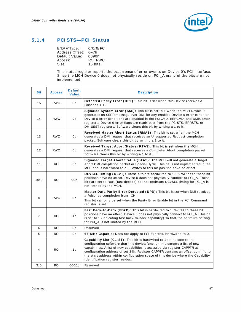
Datasheet 67
DRAM Controller Registers (D0:F0)
5.1.4 PCISTS—PCI Status
B/D/F/Type: 0/0/0/PCIAddress Offset: 6–7hDefault Value: 0090hAccess: RO, RWC Size: 16 bits
This status register reports the occurrence of error events on Device 0's PCI interface. Since the MCH Device 0 does not physically reside on PCI_A many of the bits are not implemented.
Bit AccessDefault Value
Description
15 RWC 0bDetected Parity Error (DPE): This bit is set when this Device receives a Poisoned TLP.
14 RWC 0b
Signaled System Error (SSE): This bit is set to 1 when the MCH Device 0 generates an SERR message over DMI for any enabled Device 0 error condition. Device 0 error conditions are enabled in the PCICMD, ERRCMD, and DMIUEMSK registers. Device 0 error flags are read/reset from the PCISTS, ERRSTS, or DMIUEST registers. Software clears this bit by writing a 1 to it.
13 RWC 0bReceived Master Abort Status (RMAS): This bit is set when the MCH generates a DMI request that receives an Unsupported Request completion packet. Software clears this bit by writing a 1 to it.
12 RWC 0bReceived Target Abort Status (RTAS): This bit is set when the MCH generates a DMI request that receives a Completer Abort completion packet. Software clears this bit by writing a 1 to it.
11 RO 0bSignaled Target Abort Status (STAS): The MCH will not generate a Target Abort DMI completion packet or Special Cycle. This bit is not implemented in the MCH and is hardwired to a 0. Writes to this bit position have no effect.
10:9 RO 00b
DEVSEL Timing (DEVT): These bits are hardwired to "00". Writes to these bit positions have no affect. Device 0 does not physically connect to PCI_A. These bits are set to "00" (fast decode) so that optimum DEVSEL timing for PCI_A is not limited by the MCH.
8 RWC 0b
Master Data Parity Error Detected (DPD): This bit is set when DMI received a Poisoned completion from ICH.This bit can only be set when the Parity Error Enable bit in the PCI Command register is set.
7 RO 1b
Fast Back-to-Back (FB2B): This bit is hardwired to 1. Writes to these bit positions have no effect. Device 0 does not physically connect to PCI_A. This bit is set to 1 (indicating fast back-to-back capability) so that the optimum setting for PCI_A is not limited by the MCH.
6 RO 0b Reserved
5 RO 0b 66 MHz Capable: Does not apply to PCI Express. Hardwired to 0.
4 RO 1b
Capability List (CLIST): This bit is hardwired to 1 to indicate to the configuration software that this device/function implements a list of new capabilities. A list of new capabilities is accessed via register CAPPTR at configuration address offset 34h. Register CAPPTR contains an offset pointing to the start address within configuration space of this device where the Capability Identification register resides.
3:0 RO 0000b Reserved

DRAM Controller Registers (D0:F0)
68 Datasheet
5.1.5 RID—Revision Identification
B/D/F/Type: 0/0/0/PCIAddress Offset: 8hDefault Value: 00hAccess: RO Size: 8 bits
This register contains the revision number of the MCH Device 0. These bits are read only and writes to this register have no effect.
5.1.6 CC—Class Code
B/D/F/Type: 0/0/0/PCIAddress Offset: 9–BhDefault Value: 060000hAccess: RO Size: 24 bits
This register identifies the basic function of the device, a more specific sub-class, and a register-specific programming interface.
5.1.7 MLT—Master Latency Timer
B/D/F/Type: 0/0/0/PCIAddress Offset: DhDefault Value: 00hAccess: RO Size: 8 bits
Device 0 in the MCH is not a PCI master. Therefore this register is not implemented.
Bit AccessDefault Value
Description
7:0 RO 00hRevision Identification Number (RID): This is an 8-bit value that indicates the revision identification number for the MCH Device 0.
Bit AccessDefault Value
Description
23:16 RO 06hBase Class Code (BCC): This is an 8-bit value that indicates the base class code for the MCH. This code has the value 06h, indicating a Bridge device.
15:8 RO 00hSub-Class Code (SUBCC): This is an 8-bit value that indicates the category of Bridge into which the MCH falls. The code is 00h indicating a Host Bridge.
7:0 RO 00hProgramming Interface (PI): This is an 8-bit value that indicates the programming interface of this device. This value does not specify a particular register set layout and provides no practical use for this device.
Bit AccessDefault Value
Description
7:0 RO 00h Reserved
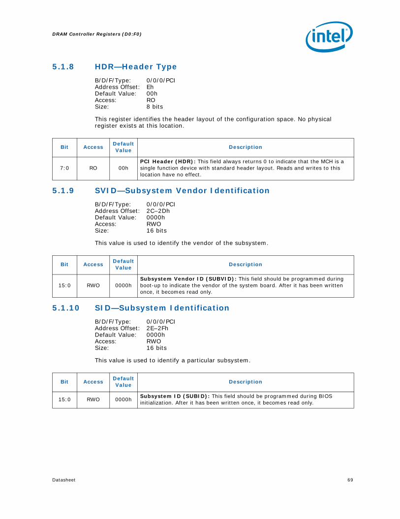
Datasheet 69
DRAM Controller Registers (D0:F0)
5.1.8 HDR—Header Type
B/D/F/Type: 0/0/0/PCIAddress Offset: EhDefault Value: 00hAccess: RO Size: 8 bits
This register identifies the header layout of the configuration space. No physical register exists at this location.
5.1.9 SVID—Subsystem Vendor Identification
B/D/F/Type: 0/0/0/PCIAddress Offset: 2C–2DhDefault Value: 0000hAccess: RWO Size: 16 bits
This value is used to identify the vendor of the subsystem.
5.1.10 SID—Subsystem Identification
B/D/F/Type: 0/0/0/PCIAddress Offset: 2E–2FhDefault Value: 0000hAccess: RWO Size: 16 bits
This value is used to identify a particular subsystem.
Bit AccessDefault Value
Description
7:0 RO 00hPCI Header (HDR): This field always returns 0 to indicate that the MCH is a single function device with standard header layout. Reads and writes to this location have no effect.
Bit AccessDefault Value
Description
15:0 RWO 0000hSubsystem Vendor ID (SUBVID): This field should be programmed during boot-up to indicate the vendor of the system board. After it has been written once, it becomes read only.
Bit AccessDefault Value
Description
15:0 RWO 0000hSubsystem ID (SUBID): This field should be programmed during BIOS initialization. After it has been written once, it becomes read only.

DRAM Controller Registers (D0:F0)
70 Datasheet
5.1.11 CAPPTR—Capabilities Pointer
B/D/F/Type: 0/0/0/PCIAddress Offset: 34hDefault Value: E0hAccess: RO Size: 8 bits
The CAPPTR provides the offset that is the pointer to the location of the first device capability in the capability list.
5.1.12 PXPEPBAR—PCI Express* Egress Port Base Address
B/D/F/Type: 0/0/0/PCIAddress Offset: 40–47hDefault Value: 0000000000000000hAccess: RO, RW/L Size: 64 bits
This is the base address for the PCI Express Egress Port MMIO Configuration space. There is no physical memory within this 4 KB window that can be addressed. The 4 KB reserved by this register does not alias to any PCI 2.3 compliant memory mapped space. On reset, the EGRESS port MMIO configuration space is disabled and must be enabled by writing a 1 to PXPEPBAREN [Dev 0, offset 40h, bit 0]
All the bits in this register are locked in Intel® TXT mode.
Bit AccessDefault Value
Description
7:0 RO E0hCapabilities Pointer (CAPPTR): Pointer to the offset of the first capability ID register block. In this case the first capability is the product-specific Capability Identifier (CAPID0).
Bit AccessDefault Value
Description
63:36 RO 0000000h Reserved
35:12 RW/L 000000h
PCI Express Egress Port MMIO Base Address (PXPEPBAR): This field corresponds to bits 35 to 12 of the base address PCI Express Egress Port MMIO configuration space. BIOS will program this register resulting in a base address for a 4 KB block of contiguous memory address space. This register ensures that a naturally aligned 4KB space is allocated within the first 64 GB of addressable memory space. System Software uses this base address to program the MCH MMIO register set. All the bits in this register are locked in Intel TXT mode.
11:1 RO 000h Reserved
0 RW/L 0b
PXPEPBAR Enable (PXPEPBAREN): 0 = PXPEPBAR is disabled and does not claim any memory1 = PXPEPBAR memory mapped accesses are claimed and decoded
appropriatelyThis register is locked by Intel TXT.

Datasheet 71
DRAM Controller Registers (D0:F0)
5.1.13 MCHBAR—MCH Memory Mapped Register Range Base
B/D/F/Type: 0/0/0/PCIAddress Offset: 48–4FhDefault Value: 0000000000000000hAccess: RO, RW/L Size: 64 bits
This is the base address for the MCH Memory Mapped Configuration space. There is no physical memory within this 16KB window that can be addressed. The 16 KB reserved by this register does not alias to any PCI 2.3 compliant memory mapped space. On reset, the MCH MMIO Memory Mapped Configuration space is disabled and must be enabled by writing a 1 to MCHBAREN [Dev 0, offset48h, bit 0]
All the bits in this register are locked in Intel TXT mode.
The register space contains memory control, initialization, timing, and buffer strength registers; clocking registers; and power and thermal management registers. The 16 KB space reserved by the MCHBAR register is not accessible during Intel TXT mode of operation or if the ME security lock is asserted (MESMLCK.ME_SM_lock at PCI device 0, function 0, offset F4h) except for the following offset ranges.
02B8h to 02BFh: Channel 0 Throttle Counter Status Registers
06B8h to 06BFh: Channel 1 Throttle Counter Status Registers
0CD0h to 0CFFh: Thermal Sensor Control Registers
3000h to 3FFFh: Unlocked registers for future expansion
Bit AccessDefault Value
Description
63:36 RO 0000000h Reserved
35:14 RW/L 000000h
MCH Memory Mapped Base Address (MCHBAR): This field corresponds to bits 35:14 of the base address MCH Memory Mapped configuration space. BIOS will program this register resulting in a base address for a 16 KB block of contiguous memory address space. This register ensures that a naturally aligned 16 KB space is allocated within the first 64 GB of addressable memory space. System Software uses this base address to program the MCH Memory Mapped register set. All the bits in this register are locked in Intel TXT mode.
13:1 RO 0000h Reserved
0 RW/L 0b
MCHBAR Enable (MCHBAREN): 0 = MCHBAR is disabled and does not claim any memory1 = MCHBAR memory mapped accesses are claimed and decoded
appropriatelyThis register is locked by Intel TXT.
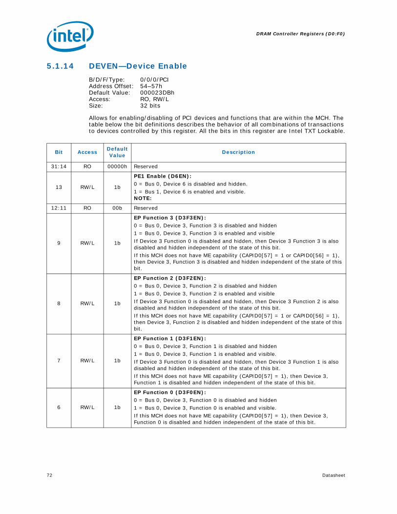
DRAM Controller Registers (D0:F0)
72 Datasheet
5.1.14 DEVEN—Device Enable
B/D/F/Type: 0/0/0/PCIAddress Offset: 54–57hDefault Value: 000023DBhAccess: RO, RW/L Size: 32 bits
Allows for enabling/disabling of PCI devices and functions that are within the MCH. The table below the bit definitions describes the behavior of all combinations of transactions to devices controlled by this register. All the bits in this register are Intel TXT Lockable.
Bit AccessDefault Value
Description
31:14 RO 00000h Reserved
13 RW/L 1b
PE1 Enable (D6EN): 0 = Bus 0, Device 6 is disabled and hidden.1 = Bus 1, Device 6 is enabled and visible. NOTE:
12:11 RO 00b Reserved
9 RW/L 1b
EP Function 3 (D3F3EN): 0 = Bus 0, Device 3, Function 3 is disabled and hidden 1 = Bus 0, Device 3, Function 3 is enabled and visible If Device 3 Function 0 is disabled and hidden, then Device 3 Function 3 is also disabled and hidden independent of the state of this bit. If this MCH does not have ME capability (CAPID0[57] = 1 or CAPID0[56] = 1), then Device 3, Function 3 is disabled and hidden independent of the state of this bit.
8 RW/L 1b
EP Function 2 (D3F2EN): 0 = Bus 0, Device 3, Function 2 is disabled and hidden 1 = Bus 0, Device 3, Function 2 is enabled and visible If Device 3 Function 0 is disabled and hidden, then Device 3 Function 2 is also disabled and hidden independent of the state of this bit. If this MCH does not have ME capability (CAPID0[57] = 1 or CAPID0[56] = 1), then Device 3, Function 2 is disabled and hidden independent of the state of this bit.
7 RW/L 1b
EP Function 1 (D3F1EN): 0 = Bus 0, Device 3, Function 1 is disabled and hidden 1 = Bus 0, Device 3, Function 1 is enabled and visible. If Device 3 Function 0 is disabled and hidden, then Device 3 Function 1 is also disabled and hidden independent of the state of this bit.If this MCH does not have ME capability (CAPID0[57] = 1), then Device 3, Function 1 is disabled and hidden independent of the state of this bit.
6 RW/L 1b
EP Function 0 (D3F0EN): 0 = Bus 0, Device 3, Function 0 is disabled and hidden 1 = Bus 0, Device 3, Function 0 is enabled and visible. If this MCH does not have ME capability (CAPID0[57] = 1), then Device 3, Function 0 is disabled and hidden independent of the state of this bit.

Datasheet 73
DRAM Controller Registers (D0:F0)
5.1.15 PCIEXBAR—PCI Express* Register Range Base Address
B/D/F/Type: 0/0/0/PCIAddress Offset: 60–67hDefault Value: 00000000E0000000hAccess: RO, RW/L, RW/L/K Size: 64 bits
This is the base address for the PCI Express configuration space. This window of addresses contains the 4 KB of configuration space for each PCI Express device that can potentially be part of the PCI Express Hierarchy associated with the MCH. There is not actual physical memory within this window of up to 256 MB that can be addressed. The actual length is determined by a field in this register. Each PCI Express Hierarchy requires a PCI Express BASE register. The MCH supports one PCI Express hierarchy. The region reserved by this register does not alias to any PCI 2.3 compliant memory mapped space.
On reset, this register is disabled and must be enabled by writing a 1 to the enable field in this register. This base address shall be assigned on a boundary consistent with the number of buses (defined by the Length field in this register), above TOLUD and still within 64 bit addressable memory space. All other bits not decoded are read only 0. The PCI Express Base Address cannot be less than the maximum address written to the Top of physical memory register (TOLUD). Software must guarantee that these ranges do not overlap with known ranges located above TOLUD. Software must ensure that the sum of Length of enhanced configuration region + TOLUD + (other known ranges reserved above TOLUD) is not greater than the 64-bit addressable limit of 64 GB. In general system implementation and number of PCI/PCI express/PCI-X buses supported in the hierarchy will dictate the length of the region.
All the Bits in this register are locked in Intel TXT mode.
5:2 RO 0s Reserved
1 RW/L 1bPCI Express Port (D1EN): 0 = Bus 0, Device 1, Function 0 is disabled and hidden. Bus 0, Device 1, Function 0 is enabled and visible.
0 RO 1bHost Bridge (D0EN): Bus 0, Device 0, Function 0 may not be disabled and is therefore hardwired to 1.
Bit AccessDefault Value
Description

DRAM Controller Registers (D0:F0)
74 Datasheet
Bit AccessDefault Value
Description
63:36 RO 0000000h Reserved
35:28 RW/L 0Eh
PCI Express Base Address (PCIEXBAR): This field corresponds to bits [35:28] of the base address for PCI Express enhanced configuration space. BIOS will program this register resulting in a base address for a contiguous memory address space; size is defined by bits [2:1] of this register.This Base address shall be assigned on a boundary consistent with the number of buses (defined by the Length field in this register) above TOLUD and still within 64-bit addressable memory space. The address bits decoded depend on the length of the region defined by this register.This register is locked by Intel TXT.The address used to access the PCI Express configuration space for a specific device can be determined as follows: PCI Express Base Address + Bus Number * 1MB + Device Number * 32KB + Function Number * 4KB The address used to access the PCI Express configuration space for Device 1 in this component would be PCI Express Base Address + 0 * 1MB + 1 * 32KB + 0 * 4KB = PCI Express Base Address + 32KB. Remember that this address is the beginning of the 4KB space that contains both the PCI compatible configuration space and the PCI Express extended configuration space.All the Bits in this register are locked in Intel TXT mode.
27 RW/L 0b128MB Base Address Mask (128ADMSK): This bit is either part of the PCI Express Base Address (R/W) or part of the Address Mask (RO, read 0b), depending on the value of bits [2:1] in this register.
26 RW/L 0b64MB Base Address Mask (64ADMSK): This bit is either part of the PCI Express Base Address (R/W) or part of the Address Mask (RO, read 0b), depending on the value of bits [2:1] in this register.
25:3 RO 000000h Reserved
2:1 RW/L/K 00b
Length (LENGTH): This Field describes the length of this region.Enhanced Configuration Space Region/Buses Decoded00 = 256 MB (buses 0-255). Bits [31:28] are decoded in the PCI Express
Base Address Field01 = 128 MB (Buses 0–127). Bits [31:27] are decoded in the PCI Express
Base Address Field.10 = 64 MB (Buses 0–63). Bits [31:26] are decoded in the PCI Express Base
Address Field.11 = ReservedThis register is locked by Intel TXT.
0 RW/L 0b
PCIEXBAR Enable (PCIEXBAREN): 0 = The PCIEXBAR register is disabled. Memory read and write transactions
proceed as if there were no PCIEXBAR register. PCIEXBAR bits [35:26] are R/W with no functionality behind them.
1 = The PCIEXBAR register is enabled. Memory read and write transactions whose address bits [35:26] match PCIEXBAR will be translated to configuration reads and writes within the MCH. These Translated cycles are routed as shown in the table above.
This register is locked by Intel TXT.

Datasheet 75
DRAM Controller Registers (D0:F0)
5.1.16 DMIBAR—Root Complex Register Range Base Address
B/D/F/Type: 0/0/0/PCIAddress Offset: 68–6FhDefault Value: 0000000000000000hAccess: RO, RW/L Size: 64 bits
This is the base address for the Root Complex configuration space. This window of addresses contains the Root Complex Register set for the PCI Express Hierarchy associated with the MCH. There is no physical memory within this 4 KB window that can be addressed. The 4 KB reserved by this register does not alias to any PCI 2.3 compliant memory mapped space. On reset, the Root Complex configuration space is disabled and must be enabled by writing a 1 to DMIBAREN [Dev 0, offset 68h, bit 0]. All the Bits in this register are locked in Intel TXT mode.
Bit AccessDefault Value
Description
63:36 RO 0000000h Reserved
35:12 RW/L 000000h
DMI Base Address (DMIBAR): This field corresponds to bits 35:12 of the base address DMI configuration space. BIOS will program this register resulting in a base address for a 4 KB block of contiguous memory address space. This register ensures that a naturally aligned 4KB space is allocated within the first 64 GB of addressable memory space. System Software uses this base address to program the DMI register set. All the Bits in this register are locked in Intel TXT mode.
11:1 RO 000h Reserved
0 RW/L 0b
DMIBAR Enable (DMIBAREN): 0 = DMIBAR is disabled and does not claim any memory1 = DMIBAR memory mapped accesses are claimed and decoded
appropriatelyThis register is locked by Intel TXT.

DRAM Controller Registers (D0:F0)
76 Datasheet
5.1.17 PAM0—Programmable Attribute Map 0
B/D/F/Type: 0/0/0/PCIAddress Offset: 90hDefault Value: 00hAccess: RO, RW/L Size: 8 bits
This register controls the read, write, and shadowing attributes of the BIOS area from 0F0000h–0FFFFFh. The MCH allows programmable memory attributes on 13 Legacy memory segments of various sizes in the 768 KB to 1 MB address range. Seven Programmable Attribute Map (PAM) Registers are used to support these features. Cacheability of these areas is controlled via the MTRR registers in the processor. Two bits are used to specify memory attributes for each memory segment. These bits apply to both host accesses and PCI initiator accesses to the PAM areas. These attributes are:
RE - Read Enable. When RE = 1, the processor read accesses to the corresponding memory segment are claimed by the MCH and directed to main memory. Conversely, when RE = 0, the host read accesses are directed to PCI_A.
WE - Write Enable. When WE = 1, the host write accesses to the corresponding memory segment are claimed by the MCH and directed to main memory. Conversely, when WE = 0, the host write accesses are directed to PCI_A.
The RE and WE attributes permit a memory segment to be Read Only, Write Only, Read/Write, or disabled. For example, if a memory segment has RE = 1 and WE = 0, the segment is Read Only. Each PAM Register controls two regions, typically 16 KB in size.
Note that the MCH may hang if a PCI Express Link Attach or DMI originated access to Read Disabled or Write Disabled PAM segments occur (due to a possible IWB to non-DRAM).
For these reasons the following critical restriction is placed on the programming of the PAM regions: At the time that a DMI or PCI Express Link Attach accesses to the PAM region may occur, the targeted PAM segment must be programmed to be both readable and writeable.
Bit AccessDefault Value
Description
7:6 RO 00b Reserved
5:4 RW/L 00b
0F0000–0FFFFF Attribute (HIENABLE): This field controls the steering of read and write cycles that address the BIOS area from 0F0000h to 0FFFFFh.00 = DRAM Disabled: All accesses are directed to DMI.01 = Read Only: All reads are sent to DRAM. All writes are forwarded to DMI.10 = Write Only: All writes are sent to DRAM. Reads are serviced by DMI.11 = Normal DRAM Operation: All reads and writes are serviced by DRAM.This register is locked by Intel TXT.
3:0 RO 0h Reserved

Datasheet 77
DRAM Controller Registers (D0:F0)
5.1.18 PAM1—Programmable Attribute Map 1
B/D/F/Type: 0/0/0/PCIAddress Offset: 91hDefault Value: 00hAccess: RO, RW/L Size: 8 bits
This register controls the read, write, and shadowing attributes of the BIOS areas from 0C0000h – 0C7FFFh.
Bit AccessDefault Value
Description
7:6 RO 00b Reserved
5:4 RW/L 00b
0C4000h–0C7FFFh Attribute (HIENABLE): This field controls the steering of read and write cycles that address the BIOS area from 0C4000h to 0C7FFFh.00 = DRAM Disabled: Accesses are directed to DMI.01 = Read Only: All reads are serviced by DRAM. All writes are forwarded to
DMI.10 = Write Only: All writes are sent to DRAM. Reads are serviced by DMI.11 = Normal DRAM Operation: All reads and writes are serviced by DRAM.This register is locked by Intel TXT.
3:2 RO 00b Reserved
1:0 RW/L 00b
0C0000h–0C3FFFh Attribute (LOENABLE): This field controls the steering of read and write cycles that address the BIOS area from 0C0000h to 0C3FFFh.00 = DRAM Disabled: Accesses are directed to DMI.01 = Read Only: All reads are serviced by DRAM. All writes are forwarded to
DMI.10 = Write Only: All writes are sent to DRAM. Reads are serviced by DMI.11 = Normal DRAM Operation: All reads and writes are serviced by DRAM.This register is locked by Intel TXT.

DRAM Controller Registers (D0:F0)
78 Datasheet
5.1.19 PAM2—Programmable Attribute Map 2
B/D/F/Type: 0/0/0/PCIAddress Offset: 92hDefault Value: 00hAccess: RO, RW/L Size: 8 bits
This register controls the read, write, and shadowing attributes of the BIOS areas from 0C8000h– 0CFFFFh.
Bit AccessDefault Value
Description
7:6 RO 00b Reserved
5:4 RW/L 00b
0CC000h–0CFFFFh Attribute (HIENABLE): 00 = DRAM Disabled: Accesses are directed to DMI.01 = Read Only: All reads are serviced by DRAM. All writes are forwarded to
DMI.10 =: Write Only: All writes are sent to DRAM. Reads are serviced by DMI.11 = Normal DRAM Operation: All reads and writes are serviced by DRAM.This register is locked by Intel TXT.
3:2 RO 00b Reserved
1:0 RW/L 00b
0C8000h–0CBFFFh Attribute (LOENABLE): This field controls the steering of read and write cycles that address the BIOS area from 0C8000h to 0CBFFFh.00 = DRAM Disabled: Accesses are directed to DMI.01 = Read Only: All reads are serviced by DRAM. All writes are forwarded to
DMI.10 = Write Only: All writes are sent to DRAM. Reads are serviced by DMI.11 = Normal DRAM Operation: All reads and writes are serviced by DRAM.This register is locked by Intel TXT.
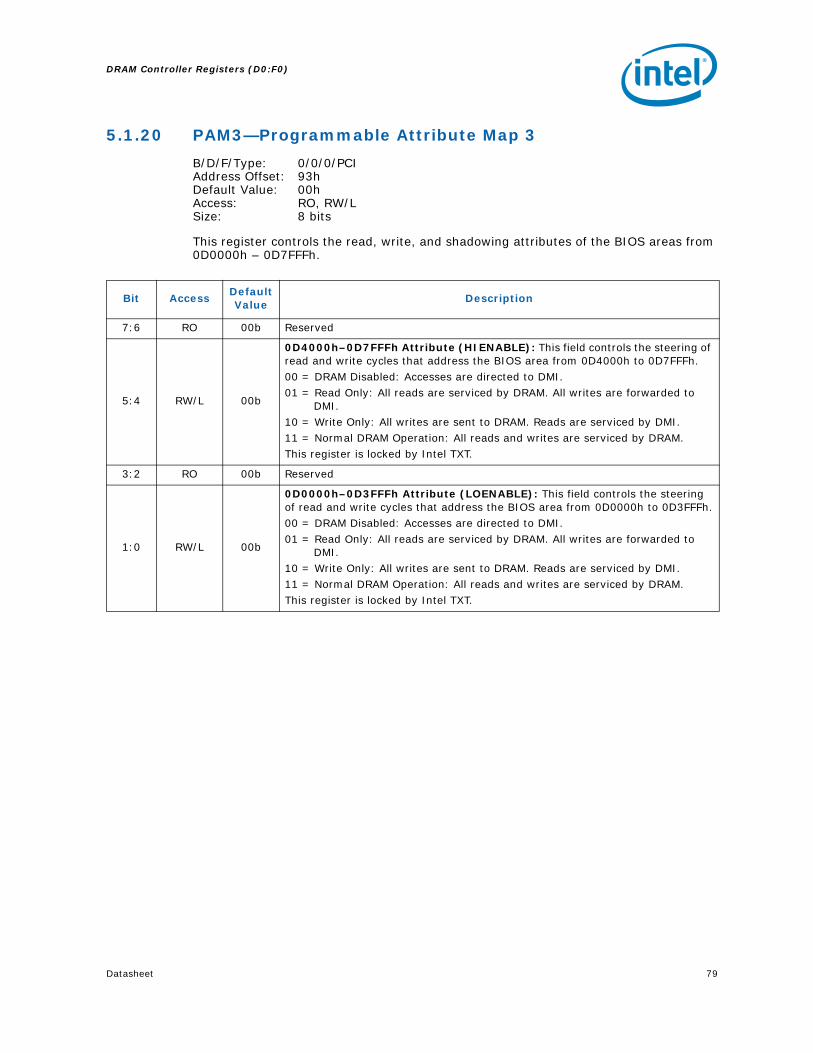
Datasheet 79
DRAM Controller Registers (D0:F0)
5.1.20 PAM3—Programmable Attribute Map 3
B/D/F/Type: 0/0/0/PCIAddress Offset: 93hDefault Value: 00hAccess: RO, RW/L Size: 8 bits
This register controls the read, write, and shadowing attributes of the BIOS areas from 0D0000h – 0D7FFFh.
Bit AccessDefault Value
Description
7:6 RO 00b Reserved
5:4 RW/L 00b
0D4000h–0D7FFFh Attribute (HIENABLE): This field controls the steering of read and write cycles that address the BIOS area from 0D4000h to 0D7FFFh.00 = DRAM Disabled: Accesses are directed to DMI.01 = Read Only: All reads are serviced by DRAM. All writes are forwarded to
DMI.10 = Write Only: All writes are sent to DRAM. Reads are serviced by DMI.11 = Normal DRAM Operation: All reads and writes are serviced by DRAM.This register is locked by Intel TXT.
3:2 RO 00b Reserved
1:0 RW/L 00b
0D0000h–0D3FFFh Attribute (LOENABLE): This field controls the steering of read and write cycles that address the BIOS area from 0D0000h to 0D3FFFh.00 = DRAM Disabled: Accesses are directed to DMI.01 = Read Only: All reads are serviced by DRAM. All writes are forwarded to
DMI.10 = Write Only: All writes are sent to DRAM. Reads are serviced by DMI.11 = Normal DRAM Operation: All reads and writes are serviced by DRAM.This register is locked by Intel TXT.

DRAM Controller Registers (D0:F0)
80 Datasheet
5.1.21 PAM4—Programmable Attribute Map 4
B/D/F/Type: 0/0/0/PCIAddress Offset: 94hDefault Value: 00hAccess: RO, RW/L Size: 8 bits
This register controls the read, write, and shadowing attributes of the BIOS areas from 0D8000h – 0DFFFFh.
Bit AccessDefault Value
Description
7:6 RO 00b Reserved
5:4 RW/L 00b
0DC000h–0DFFFFh Attribute (HIENABLE): This field controls the steering of read and write cycles that address the BIOS area from 0DC000h to 0DFFFFh.00 = DRAM Disabled: Accesses are directed to DMI.01 = Read Only: All reads are serviced by DRAM. All writes are forwarded to
DMI.
10 = Write Only: All writes are sent to DRAM. Reads are serviced by DMI.11 = Normal DRAM Operation: All reads and writes are serviced by DRAM.This register is locked by Intel TXT.
3:2 RO 00b Reserved
1:0 RW/L 00b
0D8000h–0DBFFFh Attribute (LOENABLE): This field controls the steering of read and write cycles that address the BIOS area from 0D8000h to 0DBFFFh.00 = DRAM Disabled: Accesses are directed to DMI.01 = Read Only: All reads are serviced by DRAM. All writes are forwarded to
DMI.10 = Write Only: All writes are sent to DRAM. Reads are serviced by DMI.11 = Normal DRAM Operation: All reads and writes are serviced by DRAM.This register is locked by Intel TXT.

Datasheet 81
DRAM Controller Registers (D0:F0)
5.1.22 PAM5—Programmable Attribute Map 5
B/D/F/Type: 0/0/0/PCIAddress Offset: 95hDefault Value: 00hAccess: RO, RW/L Size: 8 bits
This register controls the read, write, and shadowing attributes of the BIOS areas from 0E0000h – 0E7FFFh.
Bit AccessDefault Value
Description
7:6 RO 00b Reserved
5:4 RW/L 00b
0E4000h–0E7FFFh Attribute (HIENABLE): This field controls the steering of read and write cycles that address the BIOS area from 0E4000 to 0E7FFF.00 = DRAM Disabled: Accesses are directed to DMI.01 = Read Only: All reads are serviced by DRAM. All writes are forwarded to
DMI.10 = Write Only: All writes are sent to DRAM. Reads are serviced by DMI.11 = Normal DRAM Operation: All reads and writes are serviced by DRAM.This register is locked by Intel TXT.
3:2 RO 00b Reserved
1:0 RW/L 00b
0E0000h–0E3FFFh Attribute (LOENABLE): This field controls the steering of read and write cycles that address the BIOS area from 0E0000 to 0E3FFF.00 = DRAM Disabled: Accesses are directed to DMI.01 = Read Only: All reads are serviced by DRAM. All writes are forwarded to
DMI.10 = Write Only: All writes are sent to DRAM. Reads are serviced by DMI.11 = Normal DRAM Operation: All reads and writes are serviced by DRAM.This register is locked by Intel TXT.

DRAM Controller Registers (D0:F0)
82 Datasheet
5.1.23 PAM6—Programmable Attribute Map 6
B/D/F/Type: 0/0/0/PCIAddress Offset: 96hDefault Value: 00hAccess: RO, RW/L Size: 8 bits
This register controls the read, write, and shadowing attributes of the BIOS areas from 0E8000h–0EFFFFh.
Bit AccessDefault Value
Description
7:6 RO 00b Reserved
5:4 RW/L 00b
0EC000h–0EFFFFh Attribute (HIENABLE): This field controls the steering of read and write cycles that address the BIOS area from 0E4000h to 0E7FFFh.00 = DRAM Disabled: Accesses are directed to DMI.01 = Read Only: All reads are serviced by DRAM. All writes are forwarded to
DMI.10 = Write Only: All writes are sent to DRAM. Reads are serviced by DMI.11 = Normal DRAM Operation: All reads and writes are serviced by DRAM.This register is locked by Intel TXT.
3:2 RO 00b Reserved
1:0 RW/L 00b
0E8000h–0EBFFFh Attribute (LOENABLE): This field controls the steering of read and write cycles that address the BIOS area from 0E0000h to 0E3FFFh.00 = DRAM Disabled: Accesses are directed to DMI.01 = Read Only: All reads are serviced by DRAM. All writes are forwarded to
DMI.10 = Write Only: All writes are sent to DRAM. Reads are serviced by DMI.11 = Normal DRAM Operation: All reads and writes are serviced by DRAM.This register is locked by Intel TXT.

Datasheet 83
DRAM Controller Registers (D0:F0)
5.1.24 LAC—Legacy Access Control
B/D/F/Type: 0/0/0/PCIAddress Offset: 97hDefault Value: 00hAccess: RW/L, RO Size: 8 bits
This 8-bit register controls a fixed DRAM hole from 15–16 MB.
5.1.25 REMAPBASE—Remap Base Address Register
B/D/F/Type: 0/0/0/PCIAddress Offset: 98–99hDefault Value: 03FFhAccess: RO, RW/L Size: 16 bits
Bit AccessDefault Value
Description
7 RW/L 0b
Hole Enable (HEN): This field enables a memory hole in DRAM space. The DRAM that lies "behind" this space is not remapped.0 = No memory hole.1 = Memory hole from 15 MB to 16 MB.This bit is Intel TXT lockable.
6:0 RO 0s Reserved
Bit AccessDefault Value
Description
15:10 RO 000000b Reserved
9:0 RW/L 3FFh
Remap Base Address [35:26] (REMAPBASE): The value in this register defines the lower boundary of the Remap window. The Remap window is inclusive of this address. In the decoder A[25:0] of the Remap Base Address are assumed to be 0s. Thus the bottom of the defined memory range will be aligned to a 64MB boundary.When the value in this register is greater than the value programmed into the Remap Limit register, the Remap window is disabled.These bits are Intel TXT lockable or ME stolen Memory lockable.

DRAM Controller Registers (D0:F0)
84 Datasheet
5.1.26 REMAPLIMIT—Remap Limit Address Register
B/D/F/Type: 0/0/0/PCIAddress Offset: 9A–9BhDefault Value: 0000hAccess: RO, RW/L Size: 16 bits
Bit AccessDefault Value
Description
15:10 RO 000000b Reserved
9:0 RW/L 000h
Remap Limit Address [35:26] (REMAPLMT): The value in this register defines the upper boundary of the Remap window. The Remap window is inclusive of this address. In the decoder A[25:0] of the remap limit address are assumed to be Fs. Thus the top of the defined range will be one less than a 64 MB boundary.When the value in this register is less than the value programmed into the Remap Base register, the Remap window is disabled.These Bits are Intel TXT lockable or ME stolen Memory lockable.

Datasheet 85
DRAM Controller Registers (D0:F0)
5.1.27 SMRAM—System Management RAM Control
B/D/F/Type: 0/0/0/PCIAddress Offset: 9DhDefault Value: 02hAccess: RO, RW/L, RW, RW/L/K Size: 8 bits
The SMRAMC register controls how accesses to Compatible and Extended SMRAM spaces are treated. The Open, Close, and Lock bits function only when G_SMRAME bit is set to a 1. Also, the OPEN bit must be reset before the LOCK bit is set.
Bit AccessDefault Value
Description
7 RO 0b Reserved
6 RW/L 0b
SMM Space Open (D_OPEN): When D_OPEN=1 and D_LCK=0, the SMM space DRAM is made visible even when SMM decode is not active. This is intended to help BIOS initialize SMM space. Software should ensure that D_OPEN=1 and D_CLS=1 are not set at the same time.
5 RW 0b
SMM Space Closed (D_CLS): When D_CLS = 1 SMM space DRAM is not accessible to data references, even if SMM decode is active. Code references may still access SMM space DRAM. This will allow SMM software to reference through SMM space to update the display. Software should ensure that D_OPEN=1 and D_CLS=1 are not set at the same time.
4 RW/L/K 0b
SMM Space Locked (D_LCK): When D_LCK is set to 1 then D_OPEN is reset to 0 and D_LCK, D_OPEN, C_BASE_SEG, H_SMRAM_EN, TSEG_SZ and TSEG_EN become read only. D_LCK can be set to 1 via a normal configuration space write but can only be cleared by a Full Reset. The combination of D_LCK and D_OPEN provide convenience with security. The BIOS can use the D_OPEN function to initialize SMM space and then use D_LCK to "lock down" SMM space in the future so that no application software (or BIOS itself) can violate the integrity of SMM space, even if the program has knowledge of the D_OPEN function.
3 RW/L 0b
Global SMRAM Enable (G_SMRAME): If set to a 1, then Compatible SMRAM functions are enabled, providing 128 KB of DRAM accessible at the A0000h address while in SMM (ADSB with SMM decode). To enable Extended SMRAM function this bit has be set to 1. Refer to the section on SMM for more details. Once D_LCK is set, this bit becomes read only.
2:0 RO 010b
Compatible SMM Space Base Segment (C_BASE_SEG): This field indicates the location of SMM space. SMM DRAM is not remapped. It is simply made visible if the conditions are right to access SMM space, otherwise the access is forwarded to DMI. Since the MCH supports only the SMM space between A0000 and BFFFF, this field is hardwired to 010b.
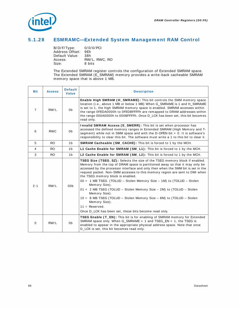
DRAM Controller Registers (D0:F0)
86 Datasheet
5.1.28 ESMRAMC—Extended System Management RAM Control
B/D/F/Type: 0/0/0/PCIAddress Offset: 9EhDefault Value: 38hAccess: RW/L, RWC, RO Size: 8 bits
The Extended SMRAM register controls the configuration of Extended SMRAM space. The Extended SMRAM (E_SMRAM) memory provides a write-back cacheable SMRAM memory space that is above 1 MB.
Bit AccessDefault Value
Description
7 RW/L 0b
Enable High SMRAM (H_SMRAME): This bit controls the SMM memory space location (i.e., above 1 MB or below 1 MB) When G_SMRAME is 1 and H_SMRAME is set to 1, the high SMRAM memory space is enabled. SMRAM accesses within the range 0FEDA0000h to 0FEDBFFFFh are remapped to DRAM addresses within the range 000A0000h to 000BFFFFh. Once D_LCK has been set, this bit becomes read only.
6 RWC 0b
Invalid SMRAM Access (E_SMERR): This bit is set when processor has accessed the defined memory ranges in Extended SMRAM (High Memory and T-segment) while not in SMM space and with the D-OPEN bit = 0. It is software's responsibility to clear this bit. The software must write a 1 to this bit to clear it.
5 RO 1b SMRAM Cacheable (SM_CACHE): This bit is forced to 1 by the MCH.
4 RO 1b L1 Cache Enable for SMRAM (SM_L1): This bit is forced to 1 by the MCH.
3 RO 1b L2 Cache Enable for SMRAM (SM_L2): This bit is forced to 1 by the MCH.
2:1 RW/L 00b
TSEG Size (TSEG_SZ): Selects the size of the TSEG memory block if enabled. Memory from the top of DRAM space is partitioned away so that it may only be accessed by the processor interface and only then when the SMM bit is set in the request packet. Non-SMM accesses to this memory region are sent to DMI when the TSEG memory block is enabled.00 = 1 MB TSEG. (TOLUD – Stolen Memory Size – 1M) to (TOLUD – Stolen
Memory Size).01 = 2 MB TSEG (TOLUD – Stolen Memory Size – 2M) to (TOLUD – Stolen
Memory Size).10 = 8 MB TSEG (TOLUD – Stolen Memory Size – 8M) to (TOLUD – Stolen
Memory Size).11 = Reserved.Once D_LCK has been set, these bits become read only.
0 RW/L 0b
TSEG Enable (T_EN): This bit is for enabling of SMRAM memory for Extended SMRAM space only. When G_SMRAME = 1 and TSEG_EN = 1, the TSEG is enabled to appear in the appropriate physical address space. Note that once D_LCK is set, this bit becomes read only.

Datasheet 87
DRAM Controller Registers (D0:F0)
5.1.29 TOM—Top of Memory
B/D/F/Type: 0/0/0/PCIAddress Offset: A0–A1hDefault Value: 0001hAccess: RO, RW/L Size: 16 bits
This Register contains the size of physical memory. BIOS determines the memory size reported to the OS using this Register.
5.1.30 TOUUD—Top of Upper Usable Dram
B/D/F/Type: 0/0/0/PCIAddress Offset: A2–A3hDefault Value: 0000hAccess: RW/L Size: 16 bits
This 16 bit register defines the Top of Upper Usable DRAM.
Configuration software must set this value to TOM minus all EP stolen memory if reclaim is disabled. If reclaim is enabled, this value must be set to reclaim limit + 1byte 64 MB aligned since reclaim limit is 64 MB aligned. Address bits 19:0 are assumed to be 000_0000h for the purposes of address comparison. The Host interface positively decodes an address towards DRAM if the incoming address is less than the value programmed in this register and greater than or equal to 4 GB.
These bits are Intel TXT lockable.
Bit AccessDefault Value
Description
15:10 RO 00h Reserved
9:0 RW/L 001h
Top of Memory (TOM): This register reflects the total amount of populated physical memory. This is NOT necessarily the highest main memory address (holes may exist in main memory address map due to addresses allocated for memory mapped IO). These bits correspond to address bits 35:26 (64MB granularity). Bits 25:0 are assumed to be 0. All the bits in this register are locked in Intel TXT mode.
Bit AccessDefault Value
Description
15:0 RW/L 0000h
TOUUD (TOUUD): This register contains bits 35:20 of an address one byte above the maximum DRAM memory above 4 GB that is usable by the operating system. Configuration software must set this value to TOM minus all EP stolen memory if reclaim is disabled. If reclaim is enabled, this value must be set to reclaim limit 64 MB aligned since reclaim limit + 1byte is 64 MB aligned. Address bits 19:0 are assumed to be 000_0000h for the purposes of address comparison. The Host interface positively decodes an address towards DRAM if the incoming address is less than the value programmed in this register and greater than 4 GB. All the Bits in this register are locked in Intel TXT mode.

DRAM Controller Registers (D0:F0)
88 Datasheet
5.1.31 BSM—Base of Stolen Memory
B/D/F/Type: 0/0/0/PCIAddress Offset: A4–A7hDefault Value: 00000000hAccess: RW/L, RO Size: 32 bits
This register contains the base address of stolen DRAM memory. BIOS determines the base of stolen memory by subtracting the stolen memory size (PCI Device 0 offset 52 bits [6:4]) from TOLUD (PCI Device 0 offset B0 bits [15:04]).
Note: This register is locked and becomes Read Only when the D_LCK bit in the SMRAM register is set.
5.1.32 TSEGMB—TSEG Memory Base
B/D/F/Type: 0/0/0/PCIAddress Offset: AC–AFhDefault Value: 00000000hAccess: RO, RW/L Size: 32 bits
This register contains the base address of TSEG DRAM memory. BIOS determines the base of TSEG memory by subtracting the TSEG size (PCI Device 0 offset 9E bits [2:1]) from stolen base (PCI Device 0 offset A4 bits [31:20]).
Once D_LCK has been set, these bits becomes read only.
Bit AccessDefault Value
Description
31:20 RW/L 000h
Base of Stolen Memory (BSM): This register contains bits 31 to 20 of the base address of stolen DRAM memory. BIOS determines the base of stolen memory by subtracting the stolen memory size (PCI Device 0, offset 52h, bits 6:4) from TOLUD (PCI Device 0, offset B0h, bits 15:4).NOTE: This register is locked and becomes Read Only when the D_LCK bit in the
SMRAM register is set.
19:0 RO 00000h Reserved
Bit AccessDefault Value
Description
31:20 RW/L 000h
TESG Memory base (TSEGMB): This register contains bits [31:20] of the base address of TSEG DRAM memory. BIOS determines the base of TSEG memory by subtracting the TSEG size (PCI Device 0 offset 9E bits [2:1]) from stolen base (PCI Device 0 offset A8 bits [31:20]). Once D_LCK has been set, these bits becomes read only.
19:0 RO 00000h Reserved
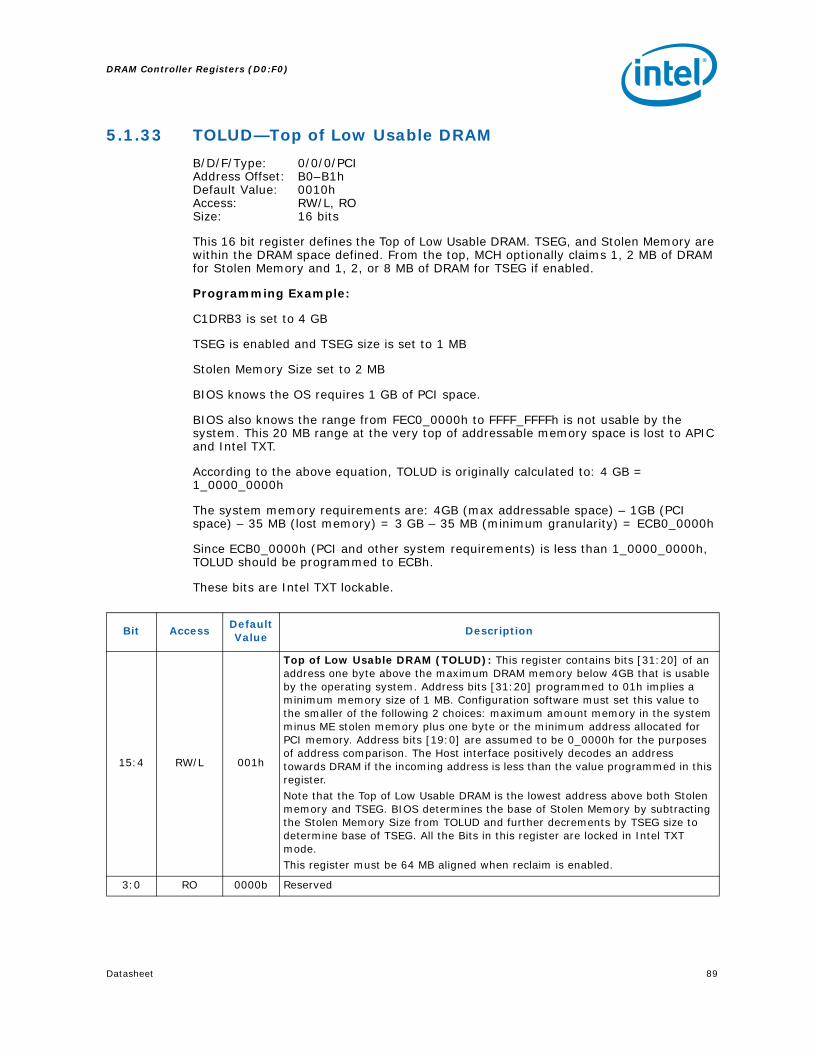
Datasheet 89
DRAM Controller Registers (D0:F0)
5.1.33 TOLUD—Top of Low Usable DRAM
B/D/F/Type: 0/0/0/PCIAddress Offset: B0–B1hDefault Value: 0010hAccess: RW/L, RO Size: 16 bits
This 16 bit register defines the Top of Low Usable DRAM. TSEG, and Stolen Memory are within the DRAM space defined. From the top, MCH optionally claims 1, 2 MB of DRAM for Stolen Memory and 1, 2, or 8 MB of DRAM for TSEG if enabled.
Programming Example:
C1DRB3 is set to 4 GB
TSEG is enabled and TSEG size is set to 1 MB
Stolen Memory Size set to 2 MB
BIOS knows the OS requires 1 GB of PCI space.
BIOS also knows the range from FEC0_0000h to FFFF_FFFFh is not usable by the system. This 20 MB range at the very top of addressable memory space is lost to APIC and Intel TXT.
According to the above equation, TOLUD is originally calculated to: 4 GB = 1_0000_0000h
The system memory requirements are: 4GB (max addressable space) – 1GB (PCI space) – 35 MB (lost memory) = 3 GB – 35 MB (minimum granularity) = ECB0_0000h
Since ECB0_0000h (PCI and other system requirements) is less than 1_0000_0000h, TOLUD should be programmed to ECBh.
These bits are Intel TXT lockable.
Bit AccessDefault Value
Description
15:4 RW/L 001h
Top of Low Usable DRAM (TOLUD): This register contains bits [31:20] of an address one byte above the maximum DRAM memory below 4GB that is usable by the operating system. Address bits [31:20] programmed to 01h implies a minimum memory size of 1 MB. Configuration software must set this value to the smaller of the following 2 choices: maximum amount memory in the system minus ME stolen memory plus one byte or the minimum address allocated for PCI memory. Address bits [19:0] are assumed to be 0_0000h for the purposes of address comparison. The Host interface positively decodes an address towards DRAM if the incoming address is less than the value programmed in this register. Note that the Top of Low Usable DRAM is the lowest address above both Stolen memory and TSEG. BIOS determines the base of Stolen Memory by subtracting the Stolen Memory Size from TOLUD and further decrements by TSEG size to determine base of TSEG. All the Bits in this register are locked in Intel TXT mode. This register must be 64 MB aligned when reclaim is enabled.
3:0 RO 0000b Reserved

DRAM Controller Registers (D0:F0)
90 Datasheet
5.1.34 ERRSTS—Error Status
B/D/F/Type: 0/0/0/PCIAddress Offset: C8–C9hDefault Value: 0000hAccess: RWC/S, RO Size: 16 bits
This register is used to report various error conditions via the SERR DMI messaging mechanism. An SERR DMI message is generated on a zero to one transition of any of these flags (if enabled by the ERRCMD and PCICMD registers).
These bits are set regardless of whether or not the SERR is enabled and generated. After the error processing is complete, the error logging mechanism can be unlocked by clearing the appropriate status bit by software writing a 1 to it.
Bit AccessDefault Value
Description
15 RO 0b Reserved
14 RWC/S 0b
Isochronous TBWRR Run Behind FIFO Full (ITCV): If set, this bit indicates a VC1 TBWRR is running behind, resulting in the slot timer to stop until the request is able to complete. If this bit is already set, then a interrupt message will not be sent on a new error event.
13 RWC/S 0b
Isochronous TBWRR Run behind FIFO Put (ITSTV): If set, this bit indicates a VC1 TBWRR request was put into the run behind. This will likely result in a resulting in a contract violation due to the MCH egress port taking too long to service the isochronous request.If this bit is already set, then a interrupt message will not be sent on a new error event.
12 RO 0b Reserved
11 RWC/S 0b
MCH Thermal Sensor Event for SMI/SCI/SERR (GTSE): This bit indicates that a MCH Thermal Sensor trip has occurred and an SMI, SCI or SERR has been generated. The status bit is set only if a message is sent based on Thermal event enables in Error command, SMI command and SCI command registers. A trip point can generate one of SMI, SCI, or SERR interrupts (two or more per event is illegal). Multiple trip points can generate the same interrupt, if software chooses this mode, subsequent trips may be lost. If this bit is already set, then an interrupt message will not be sent on a new thermal sensor event.
10 RO 0b Reserved
9 RWC/S 0bLOCK to non-DRAM Memory Flag (LCKF): When this bit is set to 1, the MCH has detected a lock operation to memory space that did not map into DRAM.
8 RO 0b Reserved
7 RWC/S 0bDRAM Throttle Flag (DTF): 1 = Indicates that a DRAM Throttling condition occurred.0 = Software has cleared this flag since the most recent throttling event.
6:2 RO 00h Reserved

Datasheet 91
DRAM Controller Registers (D0:F0)
1 RWC/S 0b
Multiple-bit DRAM ECC Error Flag (DMERR): If this bit is set to 1, a memory read data transfer had an uncorrectable multiple-bit error. When this bit is set, the address, channel number, and device number that caused the error are logged in the register. Once this bit is set, the fields are locked until the processor clears this bit by writing a 1. Software uses bits [1:0] to detect whether the logged error address is for Single or Multiple-bit error. This bit is reset on PWROK.
0 RWC/S 0b
Single-bit DRAM ECC Error Flag (DSERR): If this bit is set to 1, a memory read data transfer had a single-bit correctable error and the corrected data was sent for the access. When this bit is set the address and device number that caused the error are logged in the DEAP register. Once this bit is set the DEAP, DERRSYN, and DERRDST fields are locked to further single bit error updates until the processor clears this bit by writing a 1. A multiple bit error that occurs after this bit is set will overwrite the DEAP and DERRSYN fields with the multiple-bit error signature and the DMERR bit will also be set. A single bit error that occurs after a multi-bit error will set this bit but will not overwrite the other fields. This bit is reset on PWROK.
Bit AccessDefault Value
Description

DRAM Controller Registers (D0:F0)
92 Datasheet
5.1.35 ERRCMD—Error Command
B/D/F/Type: 0/0/0/PCIAddress Offset: CA–CBhDefault Value: 0000hAccess: RW, RO Size: 16 bits
This register controls the MCH responses to various system errors. Since the MCH does not have an SERRB signal, SERR messages are passed from the MCH to the ICH over DMI.
When a bit in this register is set, a SERR message will be generated on DMI whenever the corresponding flag is set in the ERRSTS register. The actual generation of the SERR message is globally enabled for Device 0 via the PCI Command register.
Bit AccessDefault Value
Description
15:12 RO 0h Reserved
11 RW 0b
SERR on MCH Thermal Sensor Event (TSESERR): 1 = The MCH generates a DMI SERR special cycle when bit [11] of the ERRSTS is
set. The SERR must not be enabled at the same time as the SMI for the same thermal sensor event.
0 = Reporting of this condition via SERR messaging is disabled.
10 RO 0b Reserved
9 RW 0b
SERR on LOCK to non-DRAM Memory (LCKERR): 1 = The MCH will generate a DMI SERR special cycle whenever a processor lock
cycle is detected that does not hit DRAM.0 = Reporting of this condition via SERR messaging is disabled.
8:2 RO 0s Reserved
1 RW 0b
SERR Multiple-Bit DRAM ECC Error (DMERR): 1 = The MCH generates an SERR message over DMI when it detects a multiple-
bit error reported by the DRAM controller.0 = Reporting of this condition via SERR messaging is disabled. For systems not supporting ECC this bit must be disabled.
0 RW 0b
SERR on Single-bit ECC Error (DSERR): 1 = The MCH generates an SERR special cycle over DMI when the DRAM
controller detects a single bit error.0 = Reporting of this condition via SERR messaging is disabled.For systems that do not support ECC this bit must be disabled.

Datasheet 93
DRAM Controller Registers (D0:F0)
5.1.36 SMICMD—SMI Command
B/D/F/Type: 0/0/0/PCIAddress Offset: CC–CDhDefault Value: 0000hAccess: RO, RW Size: 16 bits
This register enables various errors to generate an SMI DMI special cycle. When an error flag is set in the ERRSTS register, it can generate an SERR, SMI, or SCI DMI special cycle when enabled in the ERRCMD, SMICMD, or SCICMD registers, respectively. Note that one and only one message type can be enabled.
5.1.37 SKPD—Scratchpad Data
B/D/F/Type: 0/0/0/PCIAddress Offset: DC–DFhDefault Value: 00000000hAccess: RW Size: 32 bits
This register holds 32 writable bits with no functionality behind them. It is for the convenience of BIOS drivers.
Bit AccessDefault Value
Description
15:12 RO 0h Reserved
11 RW 0b
SMI on MCH Thermal Sensor Trip (TSTSMI): 1 = A SMI DMI special cycle is generated by MCH when the thermal sensor trip
requires an SMI. A thermal sensor trip point cannot generate more than one special cycle.
0 = Reporting of this condition via SMI messaging is disabled.
10:2 RO 000h Reserved
1 RW 0b
SMI on Multiple-Bit DRAM ECC Error (DMESMI): 1 = The MCH generates an SMI DMI message when it detects a multiple-bit error
reported by the DRAM controller.0 = Reporting of this condition via SMI messaging is disabled. For systems not
supporting ECC this bit must be disabled.
0 RW 0b
SMI on Single-bit ECC Error (DSESMI): 1 = The MCH generates an SMI DMI special cycle when the DRAM controller
detects a single bit error.0 = Reporting of this condition via SMI messaging is disabled. For systems that
do not support ECC this bit must be disabled.
Bit AccessDefault Value
Description
31:0 RW0000000
0hScratchpad Data (SKPD): 1 DWord of data storage.

DRAM Controller Registers (D0:F0)
94 Datasheet
5.1.38 CAPID0—Capability Identifier
B/D/F/Type: 0/0/0/PCIAddress Offset: E0–EBhDefault Value: 0000000181064000010C0009hAccess: RO Size: 96 bitsBIOS Optimal Default 0h
This register provides control of bits in this register are only required for customer visible component differentiation.
Bit AccessDefault Value
Description
95:78 RO 0s Reserved
77 RO 0b
Dual Channel Disable (DCD): Disables dual-channel operation0 = Dual channel operation allowed1 = Only single channel operation allowed - Only channel 0 will operate, channel
1 will be turned off and tri-stated to save power. This setting hardwires the rank population field for channel 1 to zero. (MCHBAR offset 660h, bits 20:23).
76 RO 0b
2 DIMMS per Channel Disable (2DPCD): Allows Dual-Channel operation but only supports 1 DIMM per channel.0 = 2 DIMMs per channel Enabled1 = 2 DIMMs per channel disabled. This setting hardwires bits 2 and 3 of the
rank population field for each channel to zero. (MCHBAR offset 260h, bits 22:23 for channel 0 and MCHBAR offset 660h, bits 22:23 for channel 1).
75 RO 0b Chipset Intel TXT disable (LTDIS): Chipset Intel TXT disable
74:75 RO 00b Reserved
72 RO 0b Agent Presence Disable (APD):
71 RO 0b Circuit Breaker Disable (CBD):
70 RO 0bMultiprocessor Disable (MD): 0 = MCH capable of Multiple Processors 1 = MCH capable of uni-processor only.
69 RO 0b FAN Speed Control Disable (FSCD):
68 RO 0b EastFork Disable (EFD):
67:65 RO 000b Reserved
64:62 RO 110 Reserved
61:58 RO 0000b Reserved
57 RO 0b
ME Disable (MED): 0 = ME feature is enabled1 = ME feature is disabled
56 RO 1b Reserved
55:51 RO 0s Reserved
50:49 RO 11b Reserved
48 RO 0bVT-d Disable (VTDD): 0 = Enable VT-d1 = Disable VT-d
47 RO 0b Reserved

Datasheet 95
DRAM Controller Registers (D0:F0)
46 RO 1b Reserved
45 RO 0b
Primary PCI Express Port x16 Disable (PEX16D): 0 = Capable of x16 PCI Express Port. 1 = Not Capable of x16 PCI Express port; instead PCI Express is limited to x8
and below. This causes PCI Express port to enable and train logical lanes [7:0] only. Logical lanes [15:8] are powered down, and the Max Link Width field of the Link Capability register reports x8 instead of x16. (In the case of x8 lane reversal, lanes [15:8] are active and lanes [7:0] are powered down.).
44 RO 0b
Primary PCI Express Port Disable (PEPD): 0 = There is a PCI Express Port on this MCH. Device 1 and associated memory
spaces are accessible. 1 = There is no PCI Express Port on this MCH. Device 1 and associated memory
and I/O spaces are disabled by hardwiring the D1EN field bit 1 of the Device Enable register (DEVEN Dev 0 Offset 54h). In addition, Next_Pointer = 00h, and IO cannot decode to the PCI Express interface. From a Physical Layer perspective, all 16 lanes are powered down and the link does not attempt to train.
43 RO 0b
Secondary PCI Express Port X16 Disable (PE2X16D): 0 = Capable of x16 PCI Express1 Port. 1 = Not Capable of x16 PCI Express1 port; instead PCI Express1 is limited to x8
and below. This causes PCI Express1 port to enable and train logical lanes [7:0] only. Logical lanes [15:8] are powered down, and the Max Link Width field of the Link Capability register reports x8 instead of x16. (In the case of x8 lane reversal, lanes [15:8] are active and lanes [7:0] are powered down.)
42 RO 0b
Secondary PCI Express Port Disable (PE2PD): 0 = There is a secondary PCI Express Port on this MCH. Device 6 and associated
memory spaces are accessible. 1 = There is no secondary PCI Express Port on this MCH. Device 6 and
associated memory and IO spaces are disabled by hardwiring the D6EN field bit [13] of the Device Enable register (DEVEN Dev 0 Offset 54h). All 16 lanes are powered down and the link does not attempt to train. In addition, Next_Pointer = 00h, and IO cannot decode to the PCI Express interface. From a Physical Layer perspective, all 16 lanes are powered down and the link does not attempt to train.
41 RO 0b Reserved
40 RO 0b
ECC Disable (ECCDIS): 0 = ECC capable1 = Not ECC capable. Hardwires ECC enable field, bit 7, of the CWB Control
Registers (MCHBAR Offset 243h and 643h) to "0".
39 RO 0b Reserved
38 RO 0bDDR3 Disable (DDR3D): 0 = Capable of supporting DDR3 SDRAM1 = Not Capable of supporting DDR3 SDRAM
37:35 RO 000b Reserved
34 RO 0bPrimary and Secondary PCI Express Gen 2 Disable (PEPSD): 0 = Primary and secondary PCI Express Gen 2 enabled1 = Primary and secondary PCI Express Gen 2 disabled
33:32 RO 00b Reserved
Bit AccessDefault Value
Description
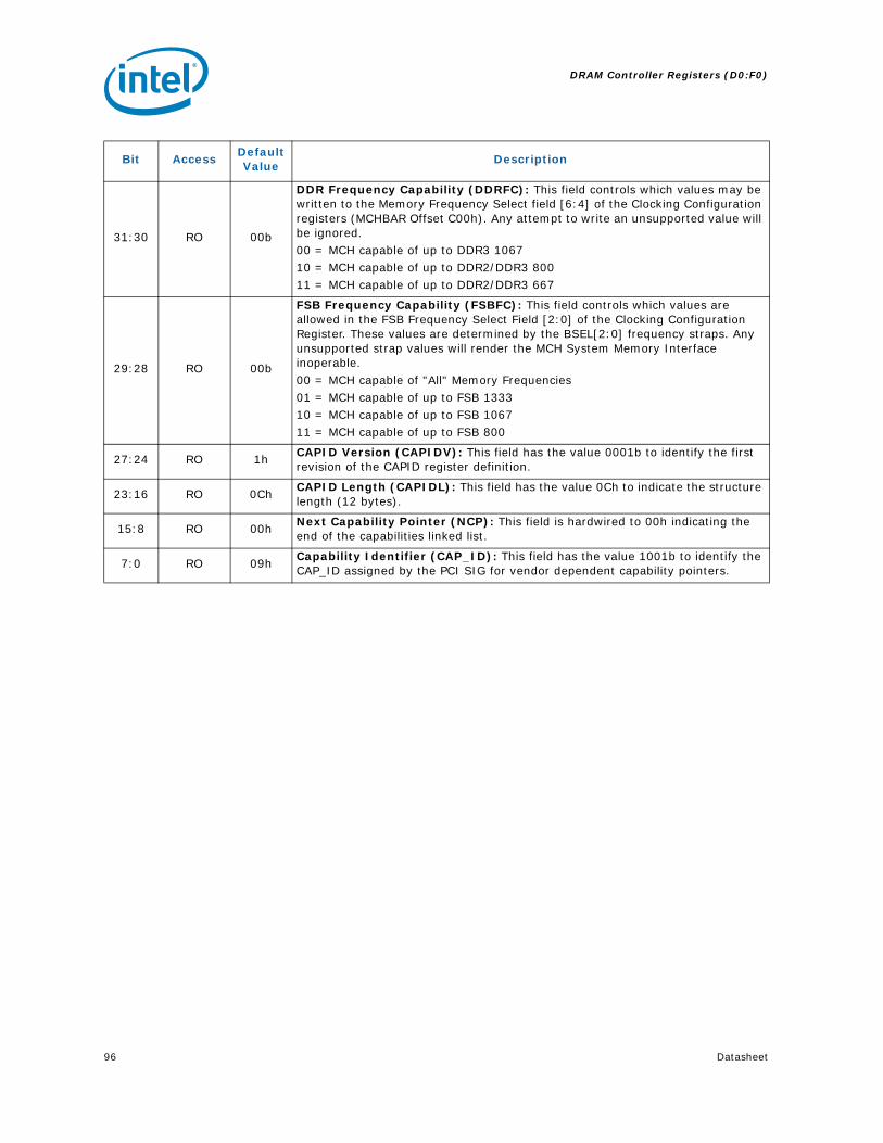
DRAM Controller Registers (D0:F0)
96 Datasheet
31:30 RO 00b
DDR Frequency Capability (DDRFC): This field controls which values may be written to the Memory Frequency Select field [6:4] of the Clocking Configuration registers (MCHBAR Offset C00h). Any attempt to write an unsupported value will be ignored.00 = MCH capable of up to DDR3 106710 = MCH capable of up to DDR2/DDR3 80011 = MCH capable of up to DDR2/DDR3 667
29:28 RO 00b
FSB Frequency Capability (FSBFC): This field controls which values are allowed in the FSB Frequency Select Field [2:0] of the Clocking Configuration Register. These values are determined by the BSEL[2:0] frequency straps. Any unsupported strap values will render the MCH System Memory Interface inoperable.00 = MCH capable of "All" Memory Frequencies01 = MCH capable of up to FSB 133310 = MCH capable of up to FSB 106711 = MCH capable of up to FSB 800
27:24 RO 1hCAPID Version (CAPIDV): This field has the value 0001b to identify the first revision of the CAPID register definition.
23:16 RO 0ChCAPID Length (CAPIDL): This field has the value 0Ch to indicate the structure length (12 bytes).
15:8 RO 00hNext Capability Pointer (NCP): This field is hardwired to 00h indicating the end of the capabilities linked list.
7:0 RO 09hCapability Identifier (CAP_ID): This field has the value 1001b to identify the CAP_ID assigned by the PCI SIG for vendor dependent capability pointers.
Bit AccessDefault Value
Description
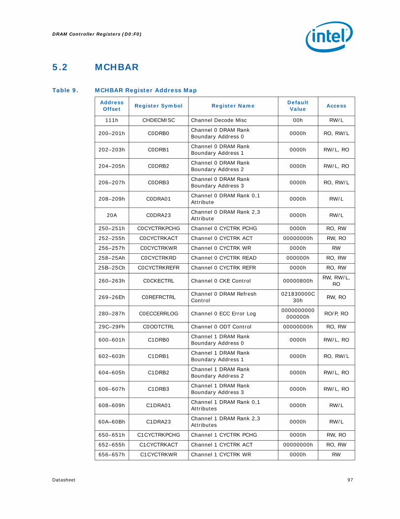
Datasheet 97
DRAM Controller Registers (D0:F0)
5.2 MCHBAR
Table 9. MCHBAR Register Address Map
Address Offset
Register Symbol Register NameDefault Value
Access
111h CHDECMISC Channel Decode Misc 00h RW/L
200–201h C0DRB0Channel 0 DRAM Rank Boundary Address 0
0000h RO, RW/L
202–203h C0DRB1Channel 0 DRAM Rank Boundary Address 1
0000h RW/L, RO
204–205h C0DRB2Channel 0 DRAM Rank Boundary Address 2
0000h RW/L, RO
206–207h C0DRB3Channel 0 DRAM Rank Boundary Address 3
0000h RO, RW/L
208–209h C0DRA01Channel 0 DRAM Rank 0,1 Attribute
0000h RW/L
20A C0DRA23Channel 0 DRAM Rank 2,3 Attribute
0000h RW/L
250–251h C0CYCTRKPCHG Channel 0 CYCTRK PCHG 0000h RO, RW
252–255h C0CYCTRKACT Channel 0 CYCTRK ACT 00000000h RW, RO
256–257h C0CYCTRKWR Channel 0 CYCTRK WR 0000h RW
258–25Ah C0CYCTRKRD Channel 0 CYCTRK READ 000000h RO, RW
25B–25Ch C0CYCTRKREFR Channel 0 CYCTRK REFR 0000h RO, RW
260–263h C0CKECTRL Channel 0 CKE Control 00000800hRW, RW/L,
RO
269–26Eh C0REFRCTRLChannel 0 DRAM Refresh Control
021830000C30h
RW, RO
280–287h C0ECCERRLOG Channel 0 ECC Error Log0000000000
000000hRO/P, RO
29C–29Fh C0ODTCTRL Channel 0 ODT Control 00000000h RO, RW
600–601h C1DRB0Channel 1 DRAM Rank Boundary Address 0
0000h RW/L, RO
602–603h C1DRB1Channel 1 DRAM Rank Boundary Address 1
0000h RO, RW/L
604–605h C1DRB2Channel 1 DRAM Rank Boundary Address 2
0000h RW/L, RO
606–607h C1DRB3Channel 1 DRAM Rank Boundary Address 3
0000h RW/L, RO
608–609h C1DRA01Channel 1 DRAM Rank 0,1 Attributes
0000h RW/L
60A–60Bh C1DRA23Channel 1 DRAM Rank 2,3 Attributes
0000h RW/L
650–651h C1CYCTRKPCHG Channel 1 CYCTRK PCHG 0000h RW, RO
652–655h C1CYCTRKACT Channel 1 CYCTRK ACT 00000000h RO, RW
656–657h C1CYCTRKWR Channel 1 CYCTRK WR 0000h RW

DRAM Controller Registers (D0:F0)
98 Datasheet
658–65Ah C1CYCTRKRD Channel 1 CYCTRK READ 000000h RW, RO
660–663h C1CKECTRL Channel 1 CKE Control 00000800hRO, RW/L,
RW
669–66Eh C1REFRCTRLChannel 1 DRAM Refresh Control
021830000C30h
RW, RO
680–687h C1ECCERRLOG Channel 1 ECC Error Log0000000000
000000hRO/P, RO
69C–69Fh C1ODTCTRL Channel 1 ODT Control 00000000h RO, RW
A00–A01h EPC0DRB0EP Channel 0 DRAM Rank Boundary Address 0
0000h RW, RO
A02–A03h EPC0DRB1EP Channel 0 DRAM Rank Boundary Address 1
0000h RW, RO
A04–A05h EPC0DRB2EP Channel 0 DRAM Rank Boundary Address 2
0000h RW, RO
A06–A07h EPC0DRB3EP Channel 0 DRAM Rank Boundary Address 3
0000h RW, RO
A08–A09h EPC0DRA01EP Channel 0 DRAM Rank 0,1 Attribute
0000h RW
A0A–A0Bh EPC0DRA23EP Channel 0 DRAM Rank 2,3 Attribute
0000h RW
A19–A1Ah EPDCYCTRKWRTPRE EPD CYCTRK WRT PRE 0000h RW, RO
A1C–A1Fh EPDCYCTRKWRTACT EPD CYCTRK WRT ACT 00000000h RO, RW
A20–A21h EPDCYCTRKWRTWR EPD CYCTRK WRT WR 0000h RW, RO
A22–A23h EPDCYCTRKWRTREF EPD CYCTRK WRT REF 0000h RO, RW
A24–A26h EPDCYCTRKWRTRD EPD CYCTRK WRT READ 000000h RW
A28–A2Ch EPDCKECONFIGREGEPD CKE related configuration registers
00E0000000h
RW
A30–A33h EPDREFCONFIG EP DRAM Refresh Configuration 40000C30h RW, RO
CD8h TSC1 Thermal Sensor Control 1 00hRW/L, RW,
RS/WC
CD9h TSC2 Thermal Sensor Control 2 00h RO, RW/L
CDAh TSS Thermal Sensor Status 00h RO
CDC–CDFh TSTTPThermal Sensor Temperature Trip Point
00000000hRO, RW, RW/L
CE2h TCO Thermal Calibration Offset 00hRW/L/K,
RW/L
CE4h THERM1 Thermal Hardware Protection 00hRW/L, RO,
RW/L/K
CEA–CEBh TIS Thermal Interrupt Status 0000h RO, RWC
CF1–CF1h TSMICMD Thermal SMI Command 00h RO, RW
F14–F17h PMSTS Power Management Status 00000000h RWC/S, RO
Table 9. MCHBAR Register Address Map
Address Offset
Register Symbol Register NameDefault Value
Access

Datasheet 99
DRAM Controller Registers (D0:F0)
5.2.1 CHDECMISC—Channel Decode Misc
B/D/F/Type: 0/0/0/MCHBARAddress Offset: 111hDefault Value: 00hAccess: RW/L Size: 8 bits
This register provides miscellaneous CHDEC/MAGEN configuration bits.
Bit AccessDefault Value
Description
7 RW/L 0b Reserved
6:5 RW/L 00b
Enhanced Mode Select (ENHMODESEL): 00 = Swap Enabled for Bank Selects and Rank Selects01 = XOR Enabled for Bank Selects and Rank Selects10 = Swap Enabled for Bank Selects only11 = XOR Enabled for Bank Select onlyThis register is locked by ME stolen Memory lock.
4 RW/L 0b Channel 2 Enhanced Mode (CH2_ENHMODE):
3 RW/L 0b Channel 1 Enhanced Mode (CH1_ENHMODE):
2 RW/L 0b Channel 0 Enhanced Mode (CH0_ENHMODE):
1 RW/L 0b Reserved
0 RW/L 0bEP Present (EPPRSNT): This bit indicates whether EP UMA is present in the system or not.This register is locked by ME stolen Memory lock.

DRAM Controller Registers (D0:F0)
100 Datasheet
5.2.2 C0DRB0—Channel 0 DRAM Rank Boundary Address 0
B/D/F/Type: 0/0/0/MCHBARAddress Offset: 200–201hDefault Value: 0000hAccess: RO, RW/L Size: 16 bits
The DRAM Rank Boundary Registers define the upper boundary address of each DRAM rank with a granularity of 64MB. Each rank has its own single-word DRB register. These registers are used to determine which chip select will be active for a given address. Channel and rank map:
ch0 rank0: 200hch0 rank1: 202hch0 rank2: 204hch0 rank3: 206hch1 rank0: 600hch1 rank1: 602hch1 rank2: 604hch1 rank3: 606h
Programming guide:
Non-stacked mode:
If Channel 0 is empty, all of the C0DRBs are programmed with 00h.
C0DRB0 = Total memory in ch0 rank0 (in 64MB increments)
C0DRB1 = Total memory in ch0 rank0 + ch0 rank1 (in 64MB increments)
and so on.
If Channel 1 is empty, all of the C1DRBs are programmed with 00h.
C1DRB0 = Total memory in ch1 rank0 (in 64MB increments)
C1DRB1 = Total memory in ch1 rank0 + ch1 rank1 (in 64MB increments)
and so on.
Stacked mode:
CODRBs:
Similar to Non-stacked mode.
C1DRB0, C1DRB1 and C1DRB2:
They are also programmed similar to non-stacked mode. Only exception is, the DRBs corresponding to the topmost populated rank and the (unpopulated) higher ranks in Channel 1 must be programmed with the value of the total Channel 1 population plus the value of total Channel 0 population (C0DRB3).
Example: If only ranks 0 and 1 are populated in Ch1 in stacked mode, then
C1DRB0 = Total memory in ch1 rank0 (in 64MB increments)

Datasheet 101
DRAM Controller Registers (D0:F0)
C1DRB1 = C0DRB3 + Total memory in ch1 rank0 + ch1 rank1 (in 64MB increments) (rank 1 is the topmost populated rank)
C1DRB2 = C1DRB1
C1DRB3 = C1DRB1
C1DRB3:
C1DRB3 = C0DRB3 + Total memory in Channel 1.
5.2.3 C0DRB1—Channel 0 DRAM Rank Boundary Address 1
B/D/F/Type: 0/0/0/MCHBARAddress Offset: 202–203hDefault Value: 0000hAccess: RW/L, RO Size: 16 bits
See C0DRB0 register.
Bit AccessDefault Value
Description
15:10 RO 000000b Reserved
9:0 RW/L 000h
Channel 0 Dram Rank Boundary Address 0 (C0DRBA0): This register defines the DRAM rank boundary for rank0 of Channel 0 (64 MB granularity)=R0R0 = Total rank0 memory size/64MBR1 = Total rank1 memory size/64MBR2 = Total rank2 memory size/64MBR3 = Total rank3 memory size/64MBThis register is locked by ME stolen Memory lock.
Bit AccessDefault Value
Description
15:10 RO 000000b Reserved
9:0 RW/L 000h
Channel 0 Dram Rank Boundary Address 1 (C0DRBA1): This field defines the DRAM rank boundary for rank1 of Channel 0 (64 MB granularity)=(R1 + R0)R0 = Total rank0 memory size/64MBR1 = Total rank1 memory size/64MBR2 = Total rank2 memory size/64MBR3 = Total rank3 memory size/64MBThis register is locked by ME stolen Memory lock.
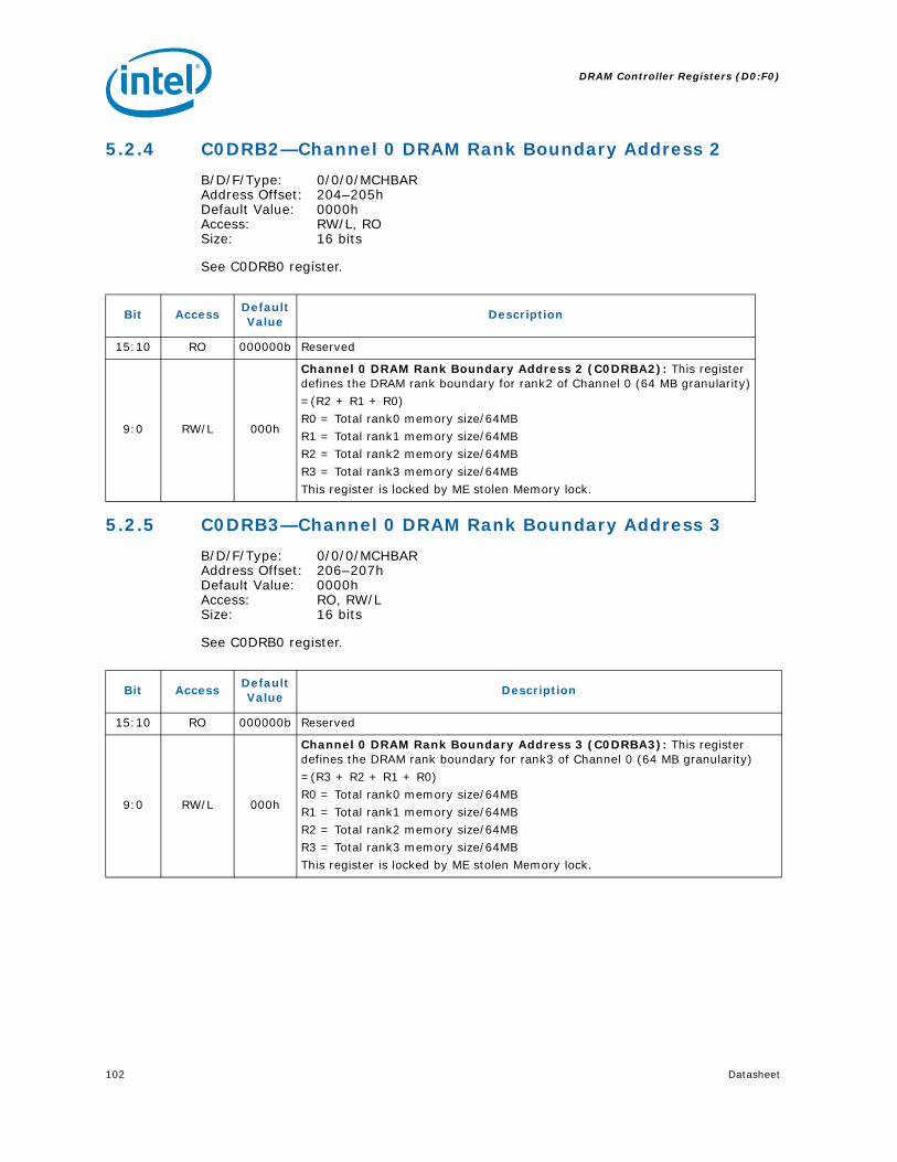
DRAM Controller Registers (D0:F0)
102 Datasheet
5.2.4 C0DRB2—Channel 0 DRAM Rank Boundary Address 2
B/D/F/Type: 0/0/0/MCHBARAddress Offset: 204–205hDefault Value: 0000hAccess: RW/L, RO Size: 16 bits
See C0DRB0 register.
5.2.5 C0DRB3—Channel 0 DRAM Rank Boundary Address 3
B/D/F/Type: 0/0/0/MCHBARAddress Offset: 206–207hDefault Value: 0000hAccess: RO, RW/L Size: 16 bits
See C0DRB0 register.
Bit AccessDefault Value
Description
15:10 RO 000000b Reserved
9:0 RW/L 000h
Channel 0 DRAM Rank Boundary Address 2 (C0DRBA2): This register defines the DRAM rank boundary for rank2 of Channel 0 (64 MB granularity)=(R2 + R1 + R0)R0 = Total rank0 memory size/64MBR1 = Total rank1 memory size/64MBR2 = Total rank2 memory size/64MB
R3 = Total rank3 memory size/64MBThis register is locked by ME stolen Memory lock.
Bit AccessDefault Value
Description
15:10 RO 000000b Reserved
9:0 RW/L 000h
Channel 0 DRAM Rank Boundary Address 3 (C0DRBA3): This register defines the DRAM rank boundary for rank3 of Channel 0 (64 MB granularity)=(R3 + R2 + R1 + R0)R0 = Total rank0 memory size/64MBR1 = Total rank1 memory size/64MBR2 = Total rank2 memory size/64MBR3 = Total rank3 memory size/64MBThis register is locked by ME stolen Memory lock.
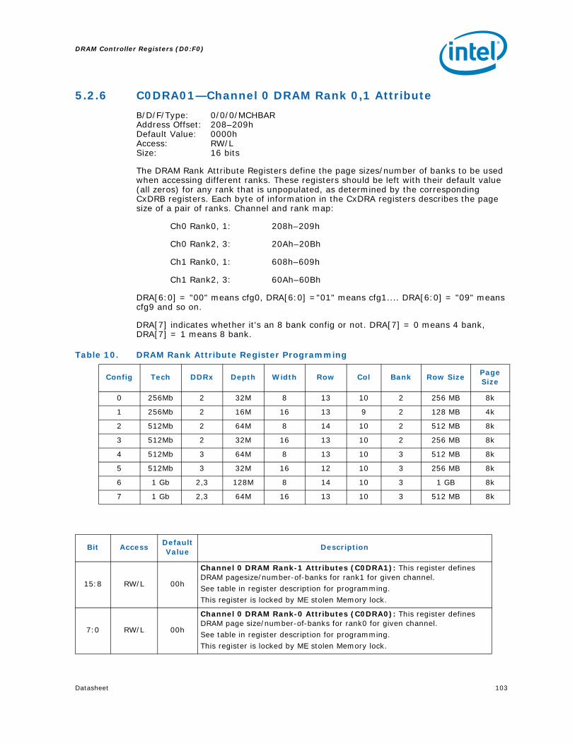
Datasheet 103
DRAM Controller Registers (D0:F0)
5.2.6 C0DRA01—Channel 0 DRAM Rank 0,1 Attribute
B/D/F/Type: 0/0/0/MCHBARAddress Offset: 208–209hDefault Value: 0000hAccess: RW/L Size: 16 bits
The DRAM Rank Attribute Registers define the page sizes/number of banks to be used when accessing different ranks. These registers should be left with their default value (all zeros) for any rank that is unpopulated, as determined by the corresponding CxDRB registers. Each byte of information in the CxDRA registers describes the page size of a pair of ranks. Channel and rank map:
Ch0 Rank0, 1: 208h–209h
Ch0 Rank2, 3: 20Ah–20Bh
Ch1 Rank0, 1: 608h–609h
Ch1 Rank2, 3: 60Ah–60Bh
DRA[6:0] = "00" means cfg0, DRA[6:0] ="01" means cfg1.... DRA[6:0] = "09" means cfg9 and so on.
DRA[7] indicates whether it's an 8 bank config or not. DRA[7] = 0 means 4 bank, DRA[7] = 1 means 8 bank.
Table 10. DRAM Rank Attribute Register Programming
Config Tech DDRx Depth Width Row Col Bank Row SizePage Size
0 256Mb 2 32M 8 13 10 2 256 MB 8k
1 256Mb 2 16M 16 13 9 2 128 MB 4k
2 512Mb 2 64M 8 14 10 2 512 MB 8k
3 512Mb 2 32M 16 13 10 2 256 MB 8k
4 512Mb 3 64M 8 13 10 3 512 MB 8k
5 512Mb 3 32M 16 12 10 3 256 MB 8k
6 1 Gb 2,3 128M 8 14 10 3 1 GB 8k
7 1 Gb 2,3 64M 16 13 10 3 512 MB 8k
Bit AccessDefault Value
Description
15:8 RW/L 00h
Channel 0 DRAM Rank-1 Attributes (C0DRA1): This register defines DRAM pagesize/number-of-banks for rank1 for given channel. See table in register description for programming. This register is locked by ME stolen Memory lock.
7:0 RW/L 00h
Channel 0 DRAM Rank-0 Attributes (C0DRA0): This register defines DRAM page size/number-of-banks for rank0 for given channel. See table in register description for programming. This register is locked by ME stolen Memory lock.

DRAM Controller Registers (D0:F0)
104 Datasheet
5.2.7 C0DRA23—Channel 0 DRAM Rank 2,3 Attribute
B/D/F/Type: 0/0/0/MCHBARAddress Offset: 20A–20BhDefault Value: 0000hAccess: RW/L Size: 16 bits
See C0DRA01 register.
5.2.8 C0CYCTRKPCHG—Channel 0 CYCTRK PCHG
B/D/F/Type: 0/0/0/MCHBARAddress Offset: 250–251hDefault Value: 0000hAccess: RO, RW Size: 16 bits
This is the Channel 0 CYCTRK Precharge registers.
Bit AccessDefault Value
Description
15:8 RW/L 00h
Channel 0 DRAM Rank-3 Attributes (C0DRA3): This register defines DRAM pagesize/number-of-banks for rank3 for given channel.See table in register description for programming.This register is locked by ME stolen Memory lock.
7:0 RW/L 00h
Channel 0 DRAM Rank-2 Attributes (C0DRA2): This register defines DRAM pagesize/number-of-banks for rank2 for given channel.See table in register description for programming.This register is locked by ME stolen Memory lock.
Bit AccessDefault Value
Description
15:11 RO 00000b Reserved
10:6 RW 00000bWrite To PRE Delayed (C0sd_cr_wr_pchg): This field indicates the minimum allowed spacing (in DRAM clocks) between the WRITE and PRE commands to the same rank-bank. This field corresponds to tWR in the DDR Specification.
5:2 RW 0000bREAD To PRE Delayed (C0sd_cr_rd_pchg): This field indicates the minimum allowed spacing (in DRAM clocks) between the READ and PRE commands to the same rank-bank
1:0 RW 00bPRE To PRE Delayed (C0sd_cr_pchg_pchg): This field indicates the minimum allowed spacing (in DRAM clocks) between two PRE commands to the same rank.

Datasheet 105
DRAM Controller Registers (D0:F0)
5.2.9 C0CYCTRKACT—Channel 0 CYCTRK ACT
B/D/F/Type: 0/0/0/MCHBARAddress Offset: 252–255hDefault Value: 00000000hAccess: RW, RO Size: 32 bits
Channel 0 CYCTRK Activate registers.
Bit AccessDefault Value
Description
31:28 RO 0h Reserved
27:22 RW 000000b
ACT Window Count (C0sd_cr_act_windowcnt): This field indicates the window duration (in DRAM clocks) during which the controller counts the # of activate commands which are launched to a particular rank. If the number of activate commands launched within this window is greater than 4, then a check is implemented to block launch of further activates to this rank for the rest of the duration of this window.
21 RW 0bMax ACT Check Disable (C0sd_cr_maxact_dischk): This field enables the check which ensures that there are no more than four activates to a particular rank in a given window.
20:17 RW 0000bACT to ACT Delayed (C0sd_cr_act_act[): This field indicates the minimum allowed spacing (in DRAM clocks) between two ACT commands to the same rank. This field corresponds to tRRD in the DDR Specification.
16:13 RW 0000b
PRE to ACT Delayed (C0sd_cr_pre_act): This field indicates the minimum allowed spacing (in DRAM clocks) between the PRE and ACT commands to the same rank-bank:12:9R/W0000bPRE-ALL to ACT Delayed. (C0sd_cr_preall_act):This field indicates the minimum allowed spacing (in DRAM clocks) between the PRE-ALL and ACT commands to the same rank. This field corresponds to tRP in the DDR Specification.
12:9 RW 0h
ALLPRE to ACT Delay (C0sd0_cr_preall_act): From the launch of a prechargeall command wait for these many # of memory clocks before launching a activate command. This field corresponds to tPALL_RP in the DDR Specification.
8:0 RW0000000
00b
REF to ACT Delayed (C0sd_cr_rfsh_act): This field indicates the minimum allowed spacing (in DRAM clocks) between REF and ACT commands to the same rank. This field corresponds to tRFC in the DDR Specification.

DRAM Controller Registers (D0:F0)
106 Datasheet
5.2.10 C0CYCTRKWR—Channel 0 CYCTRK WR
B/D/F/Type: 0/0/0/MCHBARAddress Offset: 256–257hDefault Value: 0000hAccess: RW Size: 16 bits
Channel 0 CYCTRK WR registers.
Bit AccessDefault Value
Description
15:12 RW 0hACT To Write Delay (C0sd_cr_act_wr): This field indicates the minimum allowed spacing (in DRAM clocks) between the ACT and WRITE commands to the same rank-bank. This field corresponds to tRCD_wr in the DDR Specificaiton.
11:8 RW 0hSame Rank Write To Write Delayed (C0sd_cr_wrsr_wr): This field indicates the minimum allowed spacing (in DRAM clocks) between two WRITE commands to the same rank.
7:4 RW 0h
Different Rank Write to Write Delay (C0sd_cr_wrdr_wr): This field register indicates the minimum allowed spacing (in DRAM clocks) between two WRITE commands to different ranks. This field corresponds to tWR_WR in the DDR Specification.
3:0 RW 0hREAD To WRTE Delay (C0sd_cr_rd_wr): This field indicates the minimum allowed spacing (in DRAM clocks) between the READ and WRITE commands. This field corresponds to tRD_WR.

Datasheet 107
DRAM Controller Registers (D0:F0)
5.2.11 C0CYCTRKRD—Channel 0 CYCTRK READ
B/D/F/Type: 0/0/0/MCHBARAddress Offset: 258–25AhDefault Value: 000000hAccess: RO, RW Size: 24 bits
Channel 0 CYCTRK RD registers.
5.2.12 C0CYCTRKREFR—Channel 0 CYCTRK REFR
B/D/F/Type: 0/0/0/MCHBARAddress Offset: 25B–25ChDefault Value: 0000hAccess: RO, RW Size: 16 bits
Channel 0 CYCTRK Refresh registers.
Bit AccessDefault Value
Description
23:21 RO 000b Reserved
20:17 RW 0h
Min ACT To READ Delayed (C0sd_cr_act_rd): This field indicates the minimum allowed spacing (in DRAM clocks) between the ACT and READ commands to the same rank-bank. This field corresponds to tRCD_rd in the DDR specification.
16:12 RW 00000b
Same Rank Write To READ Delayed (C0sd_cr_wrsr_rd): This field indicates the minimum allowed spacing (in DRAM clocks) between the WRITE and READ commands to the same rank. This field corresponds to tWTR in the DDR specification.
11:8 RW 0000b
Different Ranks Write To READ Delayed (C0sd_cr_wrdr_rd): This field indicates the minimum allowed spacing (in DRAM clocks) between the WRITE and READ commands to different ranks. This field corresponds to tWR_RD in the DDR specification.
7:4 RW 0000bSame Rank Read To Read Delayed (C0sd_cr_rdsr_rd): This field indicates the minimum allowed spacing (in DRAM clocks) between two READ commands to the same rank.
3:0 RW 0000bDifferent Ranks Read To Read Delayed (C0sd_cr_rddr_rd): This field indicates the minimum allowed spacing (in DRAM clocks) between two READ commands to different ranks. This field corresponds to tRD_RD.
Bit AccessDefault Value
Description
15:13 RO 000b Reserved
12:9 RW 0000bSame Rank PALL to REF Delayed (C0sd_cr_pchgall_rfsh): This field indicates the minimum allowed spacing (in DRAM clocks) between the PRE-ALL and REF commands to the same rank.
8:0 RW0000000
00b
Same Rank REF to REF Delayed (C0sd_cr_rfsh_rfsh): This field indicates the minimum allowed spacing (in DRAM clocks) between two REF commands to same ranks.

DRAM Controller Registers (D0:F0)
108 Datasheet
5.2.13 C0CKECTRL—Channel 0 CKE Control
B/D/F/Type: 0/0/0/MCHBARAddress Offset: 260–263hDefault Value: 00000800hAccess: RW, RW/L, RO Size: 32 bits
This register provides CKE controls for Channel 0.
Bit AccessDefault Value
Description
31:28 RO 0000b Reserved
27 RW 0bStart the Self-Refresh Exit Sequence (sd0_cr_srcstart): This field indicates the request to start the self-refresh exit sequence
26:24 RW 000bCKE Pulse Width Requirement in High Phase (sd0_cr_cke_pw_hl_safe): This field indicates CKE pulse width requirement in high phase. This field corresponds to tCKE (high) in the DDR specification.
23 RW/L 0b
Rank 3 Population (sd0_cr_rankpop3): 1 = Rank 3 populated0 = Rank 3 not populated This register is locked by ME stolen Memory lock.
22 RW/L 0b
Rank 2 Population (sd0_cr_rankpop2): 1 = Rank 2 populated0 = Rank 2 not populatedThis register is locked by ME stolen Memory lock.
21 RW/L 0b
Rank 1 Population (sd0_cr_rankpop1): 1 = Rank 1 populated0 = Rank 1 not populated This register is locked by ME stolen Memory lock.
20 RW/L 0b
Rank 0 Population (sd0_cr_rankpop0): 1 = Rank 0 populated0 = Rank 0 not populated This register is locked by ME stolen Memory lock.
19:17 RW 000bCKE Pulse Width Requirement in Low Phase (sd0_cr_cke_pw_lh_safe): This configuration register indicates CKE pulse width requirement in low phase.This field corresponds to tCKE (low) in the DDR specification.
16 RW 0bEnable CKE Toggle for PDN Entry/Exit (sd0_cr_pdn_enable): This bit indicates that the toggling of CKEs (for PDN entry/exit) is enabled.
15:14 RO 00b Reserved
13:10 RW 0010b
Minimum Powerdown exit to Non-Read command spacing (sd0_cr_txp): This field indicates the minimum number of clocks to wait following assertion of CKE before issuing a non-read command. 1010–1111 = Reserved. 0010–1001 = 2–9clocks. 0000–0001 = Reserved.
9:1 RW0000000
00b
Self Refresh Exit Count (sd0_cr_slfrfsh_exit_cnt): This field indicates the Self refresh exit count. (Program to 255). This field corresponds to tXSNR/tXSRD in the DDR Specification.
0 RW 0bIndicates only 1 DIMM Populated (sd0_cr_singledimmpop): This field indicates the that only 1 DIMM is populated.
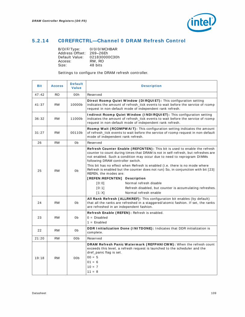
Datasheet 109
DRAM Controller Registers (D0:F0)
5.2.14 C0REFRCTRL—Channel 0 DRAM Refresh Control
B/D/F/Type: 0/0/0/MCHBARAddress Offset: 269–26EhDefault Value: 021830000C30hAccess: RW, RO Size: 48 bits
Settings to configure the DRAM refresh controller.
Bit AccessDefault Value
Description
47:42 RO 00h Reserved
41:37 RW 10000bDirect Rcomp Quiet Window (DIRQUIET): This configuration setting indicates the amount of refresh_tick events to wait before the service of rcomp request in non-default mode of independent rank refresh.
36:32 RW 11000bIndirect Rcomp Quiet Window (INDIRQUIET): This configuration setting indicates the amount of refresh_tick events to wait before the service of rcomp request in non-default mode of independent rank refresh.
31:27 RW 00110bRcomp Wait (RCOMPWAIT): This configuration setting indicates the amount of refresh_tick events to wait before the service of rcomp request in non-default mode of independent rank refresh.
26 RW 0b Reserved
25 RW 0b
Refresh Counter Enable (REFCNTEN): This bit is used to enable the refresh counter to count during times that DRAM is not in self-refresh, but refreshes are not enabled. Such a condition may occur due to need to reprogram DIMMs following DRAM controller switch.This bit has no effect when Refresh is enabled (i.e. there is no mode where Refresh is enabled but the counter does not run) So, in conjunction with bit [23] REFEN, the modes are:[REFEN:REFCNTEN] Description
[0:0] Normal refresh disable[0:1] Refresh disabled, but counter is accumulating refreshes.[1:X] Normal refresh enable
24 RW 0bAll Rank Refresh (ALLRKREF): This configuration bit enables (by default) that all the ranks are refreshed in a staggered/atomic fashion. If set, the ranks are refreshed in an independent fashion.
23 RW 0bRefresh Enable (REFEN): Refresh is enabled.0 = Disabled 1 = Enabled
22 RW 0bDDR Initialization Done (INITDONE): Indicates that DDR initialization is complete.
21:20 RW 00b Reserved
19:18 RW 00b
DRAM Refresh Panic Watermark (REFPANICWM): When the refresh count exceeds this level, a refresh request is launched to the scheduler and the dref_panic flag is set.00 = 501 = 610 = 711 = 8

DRAM Controller Registers (D0:F0)
110 Datasheet
17:16 RW 00b
DRAM Refresh High Watermark (REFHIGHWM): When the refresh count exceeds this level, a refresh request is launched to the scheduler and the dref_high flag is set.00 = 301 = 410 = 511 = 6
15:14 RW 00b
DRAM Refresh Low Watermark (REFLOWWM): When the refresh count exceeds this level, a refresh request is launched to the scheduler and the dref_low flag is set.00 = 101 = 210 = 311 = 4
13:0 RW00110000110000b
Refresh Counter Time Out Value (REFTIMEOUT): Program this field with a value that will provide 7.8 us at the memory clock frequency.At various memory clock frequencies, this results in the following values:
400 Mhz -> C30 hex (Default Value)533 Mhz -> 104B hex666 Mhz -> 1450 hex
Bit AccessDefault Value
Description

Datasheet 111
DRAM Controller Registers (D0:F0)
5.2.15 C0ECCERRLOG—Channel 0 ECC Error Log
B/D/F/Type: 0/0/0/MCHBARAddress Offset: 280–287hDefault Value: 0000000000000000hAccess: RO/P, RO Size: 64 bits
This register is used to store the error status information in ECC enabled configurations, along with the error syndrome and the rank/bank/row/column address information of the address block of main memory of which an error (single bit or multi-bit error) has occurred. Note that the address fields represent the address of the first single or the first multiple bit error occurrence after the error flag bits in the ERRSTS register have been cleared by software. A multiple bit error will overwrite a single bit error. Once the error flag bits are set as a result of an error, this bit field is locked and doesn't change as a result of a new error until the error flag is cleared by software. Same is the case with error syndrome field, but the following priority needs to be followed if more than one error occurs on one or more of the 4 QWs. MERR on QW0 MERR on QW1 MERR on QW2 MERR on QW3 CERR on QW0 CERR on QW1 CERR on QW2 CERR on QW3
Bit AccessDefault Value
Description
63:48 RO/P 0000hError Column Address (ERRCOL): Row address of the address block of main memory of which an error (single bit or multi-bit error) has occurred.
47:32 RO/P 0000hError Row Address (ERRROW): Row address of the address block of main memory of which an error (single bit or multi-bit error) has occurred.
31:29 RO/P 000bError Bank Address (ERRBANK): Rank address of the address block of main memory of which an error (single bit or multi-bit error) has occurred.
28:27 RO/P 00b
Error Rank Address (ERRRANK): Rank address of the address block of main memory of which an error (single bit or multi-bit error) has occurred.00 = rank 0 (DIMM0) 01 = rank 1 (DIMM0) 10 = rank 2 (DIMM1) 11 = rank 3 (DIMM1)
26:24 RO 0h Reserved
23:16 RO/P 00hError Syndrome (ERRSYND): Syndrome that describes the set of bits associated with the first failing quadword.
15:2 RO 0h Reserved
1 RO/P 0b
Multiple Bit Error Status (MERRSTS): This bit is set when an uncorrectable multiple-bit error occurs on a memory read data transfer. When this bit is set, the address that caused the error and the error syndrome are also logged and they are locked until this bit is cleared. This bit is cleared when it receives an indication that the processor has cleared the corresponding bit in the ERRSTS register.
0 RO/P 0b
Correctable Error Status (CERRSTS): This bit is set when a correctable single-bit error occurs on a memory read data transfer. When this bit is set, the address that caused the error and the error syndrome are also logged and they are locked to further single bit errors, until this bit is cleared. But, a multiple bit error that occurs after this bit is set will over-write the address/error syndrome info. This bit is cleared when it receives an indication that the processor has cleared the corresponding bit in the ERRSTS register.

DRAM Controller Registers (D0:F0)
112 Datasheet
5.2.16 C0ODTCTRL—Channel 0 ODT Control
B/D/F/Type: 0/0/0/MCHBARAddress Offset: 29C–29FhDefault Value: 00000000hAccess: RO, RW Size: 32 bits
This register provides ODT controls.
5.2.17 C1DRB0—Channel 1 DRAM Rank Boundary Address 0
B/D/F/Type: 0/0/0/MCHBARAddress Offset: 600–601hDefault Value: 0000hAccess: RW/L, RO Size: 16 bits
The operation of this register is detailed in the description for the C0DRB0 register.
Bit AccessDefault Value
Description
31:12 RO 00000h Reserved
11:8 RW 0hDRAM ODT for Read Commands (sd0_cr_odt_duration_rd): Specifies the duration in MDCLKs to assert DRAM ODT for Read Commands. The Async value should be used when the Dynamic Powerdown bit is set. Else use the Sync value.
7:4 RW 0hDRAM ODT for Write Commands (sd0_cr_odt_duration_wr): Specifies the duration in MDCLKs to assert DRAM ODT for Write Commands. The Async value should be used when the Dynamic Powerdown bit is set. Else use the Sync value.
3:0 RW 0hMCH ODT for Read Commands (sd0_cr_mchodt_duration): Specifies the duration in MDCLKs to assert MCH ODT for Read Commands
Bit AccessDefault Value
Description
15:10 RO 000000b Reserved
9:0 RW/L 000h
Channel 1 DRAM Rank Boundary Address 0 (C1DRBA0): See C0DRB0 register.In stacked mode, if this is the topmost populated rank in Channel 1, program this value to be cumulative of Ch0 DRB3.This register is locked by ME stolen Memory lock.

Datasheet 113
DRAM Controller Registers (D0:F0)
5.2.18 C1DRB1—Channel 1 DRAM Rank Boundary Address 1
B/D/F/Type: 0/0/0/MCHBARAddress Offset: 602–603hDefault Value: 0000hAccess: RO, RW/L Size: 16 bits
The operation of this register is detailed in the description for the C0DRB0 register.
5.2.19 C1DRB2—Channel 1 DRAM Rank Boundary Address 2
B/D/F/Type: 0/0/0/MCHBARAddress Offset: 604–605hDefault Value: 0000hAccess: RW/L, RO Size: 16 bits
The operation of this register is detailed in the description for the C0DRB0 register.
Bit AccessDefault Value
Description
15:10 RO 000000b Reserved
9:0 RW/L 000h
Channel 1 DRAM Rank Boundary Address 1 (C1DRBA1): See C0DRB1 register. In stacked mode, if this is the topmost populated rank in Channel 1, program this value to be cumulative of Ch0 DRB3.This register is locked by ME stolen Memory lock.
Bit AccessDefault Value
Description
15:10 RO 000000b Reserved
9:0 RW/L 000h
Channel 1 DRAM Rank Boundary Address 2 (C1DRBA2): See C0DRB2 register. In stacked mode, if this is the topmost populated rank in Channel 1, program this value to be cumulative of Ch0 DRB3.This register is locked by ME stolen Memory lock.

DRAM Controller Registers (D0:F0)
114 Datasheet
5.2.20 C1DRB3—Channel 1 DRAM Rank Boundary Address 3
B/D/F/Type: 0/0/0/MCHBARAddress Offset: 606–607hDefault Value: 0000hAccess: RW/L, RO Size: 16 bits
The operation of this register is detailed in the description for the C0DRB0 register.
5.2.21 C1DRA01—Channel 1 DRAM Rank 0,1 Attributes
B/D/F/Type: 0/0/0/MCHBARAddress Offset: 608–609hDefault Value: 0000hAccess: RW/L Size: 16 bits
The operation of this register is detailed in the description for register C0DRA01.
5.2.22 C1DRA23—Channel 1 DRAM Rank 2,3 Attributes
B/D/F/Type: 0/0/0/MCHBARAddress Offset: 60A–60BhDefault Value: 0000hAccess: RW/L Size: 16 bits
The operation of this register is detailed in the description for the C0DRA01 register.
Bit AccessDefault Value
Description
15:10 RO 000000b Reserved
9:0 RW/L 000h
Channel 1 DRAM Rank Boundary Address 3 (C1DRBA3): See C0DRB3 register. In stacked mode, this will be cumulative of Ch0 DRB3.This register is locked by ME stolen Memory lock.
Bit AccessDefault Value
Description
15:8 RW/L 00hChannel 1 DRAM Rank-1 Attributes (C1DRA1): See C0DRA1 register. This register is locked by ME stolen Memory lock.
7:0 RW/L 00hChannel 1 DRAM Rank-0 Attributes (C1DRA0): See C0DRA0 register. This register is locked by ME stolen Memory lock.
Bit AccessDefault Value
Description
15:8 RW/L 00hChannel 1 DRAM Rank-3 Attributes (C1DRA3): See C0DRA3 register. This register is locked by ME stolen Memory lock.
7:0 RW/L 00hChannel 1 DRAM Rank-2 Attributes (C1DRA2): See C0DRA2 register. This register is locked by ME stolen Memory lock.

Datasheet 115
DRAM Controller Registers (D0:F0)
5.2.23 C1CYCTRKPCHG—Channel 1 CYCTRK PCHG
B/D/F/Type: 0/0/0/MCHBARAddress Offset: 650–651hDefault Value: 0000hAccess: RW, RO Size: 16 bits
Channel 1 CYCTRK Precharge registers.
5.2.24 C1CYCTRKACT—Channel 1 CYCTRK ACT
B/D/F/Type: 0/0/0/MCHBARAddress Offset: 652–655hDefault Value: 00000000hAccess: RO, RW Size: 32 bits
Channel 1 CYCTRK ACT registers.
Bit AccessDefault Value
Description
15:11 RO 00000b Reserved
10:6 RW 00000bWrite To PRE Delayed (C1sd_cr_wr_pchg): This field indicates the minimum allowed spacing (in DRAM clocks) between the WRITE and PRE commands to the same rank-bank. This field corresponds to tWR in the DDR Specification.
5:2 RW 0000bREAD To PRE Delayed (C1sd_cr_rd_pchg): This field indicates the minimum allowed spacing (in DRAM clocks) between the READ and PRE commands to the same rank-bank
1:0 RW 00bPRE To PRE Delayed (C1sd_cr_pchg_pchg): This field indicates the minimum allowed spacing (in DRAM clocks) between two PRE commands to the same rank.
Bit AccessDefault Value
Description
31:28 RO 0h Reserved
27:22 RW 000000b
ACT Window Count (C1sd_cr_act_windowcnt): This field indicates the window duration (in DRAM clocks) during which the controller counts the # of activate commands which are launched to a particular rank. If the number of activate commands launched within this window is greater than 4, then a check is implemented to block launch of further activates to this rank for the rest of the duration of this window.
21 RW 0bMax ACT Check Disable (C1sd_cr_maxact_dischk):This field enables the check which ensures that there are no more than four activates to a particular rank in a given window.
20:17 RW 0000bACT to ACT Delayed (C1sd_cr_act_act[): This field indicates the minimum allowed spacing (in DRAM clocks) between two ACT commands to the same rank. This field corresponds to tRRD in the DDR specification.

DRAM Controller Registers (D0:F0)
116 Datasheet
5.2.25 C1CYCTRKWR—Channel 1 CYCTRK WR
B/D/F/Type: 0/0/0/MCHBARAddress Offset: 656–657hDefault Value: 0000hAccess: RW Size: 16 bits
Channel 1 CYCTRK WR registers.
16:13 RW 0000b
PRE to ACT Delayed (C1sd_cr_pre_act): This field indicates the minimum allowed spacing (in DRAM clocks) between the PRE and ACT commands to the same rank-bank:12:9R/W0000bPRE-ALL to ACT Delayed (C1sd_cr_preall_act):This field indicates the minimum allowed spacing (in DRAM clocks) between the PRE-ALL and ACT commands to the same rank. This field corresponds to tRP in the DDR Specification.
12:9 RW 0hALLPRE to ACT Delay (C1sd_cr_preall_act): From the launch of a prechargeall command wait for these many # of memory clocks before launching a activate command. This field corresponds to tPALL_RP.
8:0 RW0000000
00b
REF to ACT Delayed (C1sd_cr_rfsh_act): This field indicates the minimum allowed spacing (in DRAM clocks) between REF and ACT commands to the same rank. This field corresponds to tRFC in the DDR specification.
Bit AccessDefault Value
Description
Bit AccessDefault Value
Description
15:12 RW 0hACT To Write Delay (C1sd_cr_act_wr): This field indicates the minimum allowed spacing (in DRAM clocks) between the ACT and WRITE commands to the same rank-bank. This field corresponds to tRCD_wr in the DDR Specification.
11:8 RW 0hSame Rank Write To Write Delayed (C1sd_cr_wrsr_wr): This field register indicates the minimum allowed spacing (in DRAM clocks) between two WRITE commands to the same rank.
7:4 RW 0h
Different Rank Write to Write Delay (C1sd_cr_wrdr_wr): This field indicates the minimum allowed spacing (in DRAM clocks) between two WRITE commands to different ranks. This field corresponds to tWR_WR in the DDR Specification.
3:0 RW 0hREAD To WRTE Delay (C1sd_cr_rd_wr): This field indicates the minimum allowed spacing (in DRAM clocks) between the READ and WRITE commands. This field corresponds to tRD_WR.

Datasheet 117
DRAM Controller Registers (D0:F0)
5.2.26 C1CYCTRKRD—Channel 1 CYCTRK READ
B/D/F/Type: 0/0/0/MCHBARAddress Offset: 658–65AhDefault Value: 000000hAccess: RW, RO Size: 24 bits
Channel 1 CYCTRK READ registers.
Bit AccessDefault Value
Description
23:21 RO 0h Reserved
20:17 RW 0h
Min ACT To READ Delayed (C1sd_cr_act_rd): This field indicates the minimum allowed spacing (in DRAM clocks) between the ACT and READ commands to the same rank-bank. This field Corresponds to tRCD_rd in the DDR Specification
16:12 RW 00000b
Same Rank Write To READ Delayed (C1sd_cr_wrsr_rd): This field indicates the minimum allowed spacing (in DRAM clocks) between the WRITE and READ commands to the same rank. This field corresponds to tWTR in the DDR Specification.
11:8 RW 0000b
Different Ranks Write To READ Delayed (C1sd_cr_wrdr_rd): This field indicates the minimum allowed spacing (in DRAM clocks) between the WRITE and READ commands to different ranks. This field corresponds to tWR_RD in the DDR Specification.
7:4 RW 0000bSame Rank Read To Read Delayed (C1sd_cr_rdsr_rd): This field indicates the minimum allowed spacing (in DRAM clocks) between two READ commands to the same rank.
3:0 RW 0000bDifferent Ranks Read To Read Delayed (C1sd_cr_rddr_rd): This field indicates the minimum allowed spacing (in DRAM clocks) between two READ commands to different ranks. This field corresponds to tRD_RD.

DRAM Controller Registers (D0:F0)
118 Datasheet
5.2.27 C1CKECTRL—Channel 1 CKE Control
B/D/F/Type: 0/0/0/MCHBARAddress Offset: 660–663hDefault Value: 00000800hAccess: RO, RW/L, RW Size: 32 bits
Channel 1 CKE Control registers.
Bit AccessDefault Value
Description
31:28 RO 0h Reserved
27 RW 0bStart the Self-Refresh Exit Sequence (sd1_cr_srcstart): This bit indicates the request to start the self-refresh exit sequence
26:24 RW 000bCKE Pulse Width Requirement in High Phase (sd1_cr_cke_pw_hl_safe): This bit indicates CKE pulse width requirement in high phase. This field Corresponds to tCKE (high) in the DDR Specification.
23 RW/L 0b
Rank 3 Population (sd1_cr_rankpop3): 1 = Rank 3 populated0 = Rank 3 not populated This register is locked by ME stolen Memory lock.
22 RW/L 0b
Rank 2 Population (sd1_cr_rankpop2): 1 = Rank 2 populated0 = Rank 2 not populated This register is locked by ME stolen Memory lock.
21 RW/L 0b
Rank 1 Population (sd1_cr_rankpop1): 1 = Rank 1 populated0 = Rank 1 not populated This register is locked by ME stolen Memory lock.
20 RW/L 0b
Rank 0 Population (sd1_cr_rankpop0): 1 = Rank 0 populated0 = Rank 0 not populated This register is locked by ME stolen Memory lock.
19:17 RW 000bCKE Pulse Width Requirement in Low Phase (sd1_cr_cke_pw_lh_safe): This field indicates CKE pulse width requirement in low phase. This field Corresponds to tCKE (low) in the DDR Specification.
16 RW 0bEnable CKE Toggle for PDN Entry/Exit (sd1_cr_pdn_enable): This bit indicates that the toggling of CKEs (for PDN entry/exit) is enabled.
15:14 RO 00b Reserved
13:10 RW 0010b
Minimum Powerdown Exit to Non-Read Command Spacing (sd1_cr_txp): This field indicates the minimum number of clocks to wait following assertion of CKE before issuing a non-read command.1010–1111 = Reserved.0010–1001 = 2–9 clocks0000–0001 = Reserved.
9:1 RW0000000
00b
Self Refresh Exit Count (sd1_cr_slfrfsh_exit_cnt): This configuration register indicates the Self refresh exit count. (Program to 255)Corresponds to tXSNR/tXSRD in the DDR Specification.
0 RW 0bIndicates Only 1 DIMM Populated (sd1_cr_singledimmpop): This field indicates the that only 1 DIMM is populated.

Datasheet 119
DRAM Controller Registers (D0:F0)
5.2.28 C1REFRCTRL—Channel 1 DRAM Refresh Control
B/D/F/Type: 0/0/0/MCHBARAddress Offset: 669–66EhDefault Value: 021830000C30hAccess: RW, RO Size: 48 bits
Settings to configure the DRAM refresh controller.
Bit AccessDefault Value
Description
47:42 RO 00h Reserved
41:37 RW 10000bDirect Rcomp Quiet Window (DIRQUIET): This configuration setting indicates the amount of refresh_tick events to wait before the service of rcomp request in non-default mode of independent rank refresh.
36:32 RW 11000bIndirect Rcomp Quiet Window (INDIRQUIET): This configuration setting indicates the amount of refresh_tick events to wait before the service of rcomp request in non-default mode of independent rank refresh.
31:27 RW 00110bRcomp Wait (RCOMPWAIT): This configuration setting indicates the amount of refresh_tick events to wait before the service of rcomp request in non-default mode of independent rank refresh.
26 RO 0b Reserved
25 RW 0b
Refresh Counter Enable (REFCNTEN): This bit is used to enable the refresh counter to count during times that DRAM is not in self-refresh, but refreshes are not enabled. Such a condition may occur due to need to reprogram DIMMs following DRAM controller switch.This bit has no effect when Refresh is enabled (i.e. there is no mode where Refresh is enabled but the counter does not run) So, in conjunction with bit 23 REFEN, the modes are:[REFEN:REFCNTEN]Description
[0:0] Normal refresh disable[0:1] Refresh disabled, but counter is accumulating refreshes.[1:X] Normal refresh enable
24 RW 0bAll Rank Refresh (ALLRKREF): This configuration bit enables (by default) that all the ranks are refreshed in a staggered/atomic fashion. If set, the ranks are refreshed in an independent fashion.
23 RW 0bRefresh Enable (REFEN): Refresh is enabled.0 = Disabled1 = Enabled
22 RW 0bDDR Initialization Done (INITDONE): Indicates that DDR initialization is complete.
21:20 RO 00b Reserved
19:18 RW 00b
DRAM Refresh Panic Watermark (REFPANICWM): When the refresh count exceeds this level, a refresh request is launched to the scheduler and the dref_panic flag is set.00 = 501 = 610 = 711 = 8

DRAM Controller Registers (D0:F0)
120 Datasheet
5.2.29 C1ECCERRLOG—Channel 1 ECC Error Log
B/D/F/Type: 0/0/0/MCHBARAddress Offset: 680–687hDefault Value: 0000000000000000hAccess: RO/P, RO Size: 64 bits
This register is used to store the error status information in ECC enabled configurations, along with the error syndrome and the rank/bank/row/column address information of the address block of main memory of which an error (single bit or multi-bit error) has occurred. Note that the address fields represent the address of the first single or the first multiple bit error occurrence after the error flag bits in the ERRSTS register have been cleared by software. A multiple bit error will overwrite a single bit error. Once the error flag bits are set as a result of an error, this bit field is locked and does not change as a result of a new error until the error flag is cleared by software. Same is the case with error syndrome field, but the following priority needs to be followed if more than one error occurs on one or more of the 4 QWs. MERR on QW0, MERR on QW1, MERR on QW2, MERR on QW3, CERR on QW0, CERR on QW1, CERR on QW2, CERR on QW3.
17:16 RW 00b
DRAM Refresh High Watermark (REFHIGHWM): When the refresh count exceeds this level, a refresh request is launched to the scheduler and the dref_high flag is set.00 = 301 = 410 = 511 = 6
15:14 RW 00b
DRAM Refresh Low Watermark (REFLOWWM): When the refresh count exceeds this level, a refresh request is launched to the scheduler and the dref_low flag is set.00 = 101 = 210 = 311 = 4
13:0 RW00110000110000
b
Refresh Counter Time Out Value (REFTIMEOUT): Program this field with a value that will provide 7.8 us at the memory clock frequency.At various memory clock frequencies, this results in the following values:
400 Mhz -> C30 hex (Default Value)533 Mhz -> 104B hex666 Mhz -> 1450 hex
Bit AccessDefault Value
Description
Bit AccessDefault Value
Description
63:48 RO/P 0000hError Column Address (ERRCOL): Row address of the address block of main memory of which an error (single bit or multi-bit error) has occurred.
47:32 RO/P 0000hError Row Address (ERRROW): Row address of the address block of main memory of which an error (single bit or multi-bit error) has occurred.
31:29 RO/P 000bError Bank Address (ERRBANK): Rank address of the address block of main memory of which an error (single bit or multi-bit error) has occurred.

Datasheet 121
DRAM Controller Registers (D0:F0)
5.2.30 C1ODTCTRL—Channel 1 ODT Control
B/D/F/Type: 0/0/0/MCHBARAddress Offset: 69C–69FhDefault Value: 00000000hAccess: RO, RW Size: 32 bits
This register provides ODT controls.
28:27 RO/P 00b
Error Rank Address (ERRRANK): Rank address of the address block of main memory of which an error (single bit or multi-bit error) has occurred.00 = rank 0 (DIMM0) 01 = rank 1 (DIMM0) 10 = rank 2 (DIMM1) 11 = rank 3 (DIMM1)
26:24 RO 0h Reserved
23:16 RO/P 00hError Syndrome (ERRSYND): Syndrome that describes the set of bits associated with the first failing quadword.
15:2 RO 0h Reserved
1 RO/P 0b
Multiple Bit Error Status (MERRSTS): This bit is set when an uncorrectable multiple-bit error occurs on a memory read data transfer. When this bit is set, the address that caused the error and the error syndrome are also logged and they are locked until this bit is cleared. This bit is cleared when it receives an indication that the processor has cleared the corresponding bit in the ERRSTS register.
0 RO/P 0b
Correctable Error Status (CERRSTS): This bit is set when a correctable single-bit error occurs on a memory read data transfer. When this bit is set, the address that caused the error and the error syndrome are also logged and they are locked to further single bit errors, until this bit is cleared. But, a multiple bit error that occurs after this bit is set will over-write the address/error syndrome info. This bit is cleared when it receives an indication that the processor has cleared the corresponding bit in the ERRSTS register.
Bit AccessDefault Value
Description
Bit AccessDefault Value
Description
31:12 RO 00000h Reserved
11:8 RW 0hDRAM ODT for Read Commands (sd1_cr_odt_duration_rd): Specifies the duration in MDCLKs to assert DRAM ODT for Read Commands. The Async value should be used when the Dynamic Powerdown bit is set. Else use the Sync value.
7:4 RW 0hDRAM ODT for Write Commands (sd1_cr_odt_duration_wr): Specifies the duration in MDCLKs to assert DRAM ODT for Write Commands. The Async value should be used when the Dynamic Powerdown bit is set. Else use the Sync value.
3:0 RW 0hMCH ODT for Read Commands (sd1_cr_mchodt_duration): Specifies the duration in MDCLKs to assert MCH ODT for Read Commands.

DRAM Controller Registers (D0:F0)
122 Datasheet
5.2.31 EPC0DRB0—EP Channel 0 DRAM Rank Boundary Address 0
B/D/F/Type: 0/0/0/MCHBARAddress Offset: A00–A01hDefault Value: 0000hAccess: RW, RO Size: 16 bits
5.2.32 EPC0DRB1—EP Channel 0 DRAM Rank Boundary Address 1
B/D/F/Type: 0/0/0/MCHBARAddress Offset: A02–A03hDefault Value: 0000hAccess: RW, RO Size: 16 bits
See C0DRB0 register.
5.2.33 EPC0DRB2—EP Channel 0 DRAM Rank Boundary Address 2
B/D/F/Type: 0/0/0/MCHBARAddress Offset: A04–A05hDefault Value: 0000hAccess: RW, RO Size: 16 bits
See C0DRB0 register.
Bit AccessDefault Value
Description
15:10 RO 000000b Reserved
9:0 RW 000h Channel 0 Dram Rank Boundary Address 0 (C0DRBA0):
Bit AccessDefault Value
Description
15:10 RO 000000b Reserved
9:0 RW 000h Channel 0 Dram Rank Boundary Address 1 (C0DRBA1):
Bit AccessDefault Value
Description
15:10 RO 000000b Reserved
9:0 RW 000h Channel 0 DRAM Rank Boundary Address 2 (C0DRBA2):

Datasheet 123
DRAM Controller Registers (D0:F0)
5.2.34 EPC0DRB3—EP Channel 0 DRAM Rank Boundary Address 3
B/D/F/Type: 0/0/0/MCHBARAddress Offset: A06–A07hDefault Value: 0000hAccess: RW, RO Size: 16 bits
See C0DRB0 register.
5.2.35 EPC0DRA01—EP Channel 0 DRAM Rank 0,1 Attribute
B/D/F/Type: 0/0/0/MCHBARAddress Offset: A08–A09hDefault Value: 0000hAccess: RW Size: 16 bits
The DRAM Rank Attribute Registers define the page sizes/number of banks to be used when accessing different ranks. These registers should be left with their default value (all zeros) for any rank that is unpopulated, as determined by the corresponding CxDRB registers. Each byte of information in the CxDRA registers describes the page size of a pair of ranks. Channel and rank map:
Ch0 Rank0, 1: 108h–109h
Ch0 Rank2, 3: 10Ah–10Bh
Ch1 Rank0, 1: 188h–189h
Ch1 Rank2, 3: 18Ah–18Bh
Bit AccessDefault Value
Description
15:10 RO 000000b Reserved
9:0 RW 000h Channel 0 DRAM Rank Boundary Address 3 (C0DRBA3):
Bit AccessDefault Value
Description
15:8 RW 00hChannel 0 DRAM Rank-1 Attributes (C0DRA1): This register defines DRAM pagesize/number-of-banks for rank1 for given channel.
7:0 RW 00hChannel 0 DRAM Rank-0 Attributes (C0DRA0): This register defines DRAM pagesize/number-of-banks for rank0 for given channel.

DRAM Controller Registers (D0:F0)
124 Datasheet
5.2.36 EPC0DRA23—EP Channel 0 DRAM Rank 2,3 Attribute
B/D/F/Type: 0/0/0/MCHBARAddress Offset: A0A–A0BhDefault Value: 0000hAccess: RW Size: 16 bits
See C0DRA01 register.
5.2.37 EPDCYCTRKWRTPRE—EPD CYCTRK WRT PRE
B/D/F/Type: 0/0/0/MCHBARAddress Offset: A19–A1AhDefault Value: 0000hAccess: RW, RO Size: 16 bits
EPD CYCTRK WRT PRE Status registers.
Bit AccessDefault Value
Description
15:8 RW 00hChannel 0 DRAM Rank-3 Attributes (C0DRA3): This register defines DRAM pagesize/number-of-banks for rank3 for given channel.
7:0 RW 00hChannel 0 DRAM Rank-2 Attributes (C0DRA2): This register defines DRAM pagesize/number-of-banks for rank2 for given channel.
Bit AccessDefault Value
Description
15:11 RW 00000bACTTo PRE Delayed (C0sd_cr_act_pchg): This field indicates the minimum allowed spacing (in DRAM clocks) between the ACT and PRE commands to the same rank-bank
10:6 RW 00000bWrite To PRE Delayed (C0sd_cr_wr_pchg): This field indicates the minimum allowed spacing (in DRAM clocks) between the WRITE and PRE commands to the same rank-bank
5:2 RW 0000bREAD To PRE Delayed (C0sd_cr_rd_pchg): This field indicates the minimum allowed spacing (in DRAM clocks) between the READ and PRE commands to the same rank-bank
1:0 RO 00b Reserved

Datasheet 125
DRAM Controller Registers (D0:F0)
5.2.38 EPDCYCTRKWRTACT—EPD CYCTRK WRT ACT
B/D/F/Type: 0/0/0/MCHBARAddress Offset: A1C–A1FhDefault Value: 00000000hAccess: RO, RW Size: 32 bits
EPD CYCTRK WRT ACT Status registers.
5.2.39 EPDCYCTRKWRTWR—EPD CYCTRK WRT WR
B/D/F/Type: 0/0/0/MCHBARAddress Offset: A20–A21hDefault Value: 0000hAccess: RW, RO Size: 16 bits
EPD CYCTRK WRT WR Status registers.
Bit AccessDefault Value
Description
31:21 RO 000h Reserved
20:17 RW 0000bACT to ACT Delayed (C0sd_cr_act_act[): This configuration register indicates the minimum allowed spacing (in DRAM clocks) between two ACT commands to the same rank.
16:13 RW 0000b
PRE to ACT Delayed (C0sd_cr_pre_act): This field indicates the minimum allowed spacing (in DRAM clocks) between the PRE and ACT commands to the same rank-bank:12:9R/W0000bPRE-ALL to ACT Delayed (C0sd_cr_preall_act):This configuration register indicates the minimum allowed spacing (in DRAM clocks) between the PRE-ALL and ACT commands to the same rank.
12:9 RO 0h Reserved
8:0 RW0000000
00b
REF to ACT Delayed (C0sd_cr_rfsh_act): This configuration register indicates the minimum allowed spacing (in DRAM clocks) between REF and ACT commands to the same rank.
Bit AccessDefault Value
Description
15:12 RW 0hACT To Write Delay (C0sd_cr_act_wr): This field indicates the minimum allowed spacing (in DRAM clocks) between the ACT and WRITE commands to the same rank-bank
11:8 RW 0hSame Rank Write To Write Delayed (C0sd_cr_wrsr_wr): This field indicates the minimum allowed spacing (in DRAM clocks) between two WRITE commands to the same rank.
7:4 RO 0h Reserved
3:0 RW 0hSame Rank WRITE to READ Delay (C0sd_cr_rd_wr): This field indicates the minimum allowed spacing (in DRAM clocks) between the WRITE and READ commands to the same rank.

DRAM Controller Registers (D0:F0)
126 Datasheet
5.2.40 EPDCYCTRKWRTREF—EPD CYCTRK WRT REF
B/D/F/Type: 0/0/0/MCHBARAddress Offset: A22–A23hDefault Value: 0000hAccess: RO, RW Size: 16 bitsBIOS Optimal Default 0h
EPD CYCTRK WRT ACT Status registers.
5.2.41 EPDCYCTRKWRTRD—EPD CYCTRK WRT READ
B/D/F/Type: 0/0/0/MCHBARAddress Offset: A24–A26hDefault Value: 000000hAccess: RW Size: 24 bitsBIOS Optimal Default 000h
EPD CYCTRK WRT RD Status registers.
Bit AccessDefault Value
Description
15:9 RO 0s Reserved
8:0 RW0000000
00b
Different Rank REF to REF Delayed (C0sd_cr_rfsh_rfsh): This configuration register indicates the minimum allowed spacing (in DRAM clocks) between two REF commands to different ranks.
Bit AccessDefault Value
Description
23:23 RO 0h Reserved
22:20 RW 000bEPDunit DQS Slave DLL Enable to Read Safe (EPDSDLL2RD): Configuration setting for Read command safe from the point of enabling the slave DLLs.
19:18 RO 0h Reserved
17:14 RW 0hMin ACT To READ Delayed (C0sd_cr_act_rd): This field indicates the minimum allowed spacing (in DRAM clocks) between the ACT and READ commands to the same rank-bank
13:9 RW 00000bSame Rank READ to WRITE Delayed (C0sd_cr_wrsr_rd): This field indicates the minimum allowed spacing (in DRAM clocks) between the READ and WRITE commands.
8:6 RO 0h Reserved
5:3 RW 000bSame Rank Read To Read Delayed (C0sd_cr_rdsr_rd): This field indicates the minimum allowed spacing (in DRAM clocks) between two READ commands to the same rank.
2:0 RO 0h Reserved

Datasheet 127
DRAM Controller Registers (D0:F0)
5.2.42 EPDCKECONFIGREG—EPD CKE Related Configuration
B/D/F/Type: 0/0/0/MCHBARAddress Offset: A28–A2ChDefault Value: 00E0000000hAccess: RW Size: 40 bitsBIOS Optimal Default 0h
CKE related configuration registers For EPD.
Bit AccessDefault Value
Description
39:35 RW 00000bEPDunit TXPDLL Count (EPDTXPDLL): Specifies the delay from precharge power down exit to a command that requires the DRAM DLL to be operational. The commands are read/write.
34:32 RW 000bEPDunit TXP Count (EPDCKETXP): Specifies the timing requirement for Active power down exit or fast exit pre-charge power down exit to any command or slow exit pre-charge power down to Non-DLL (rd/wr/odt) command.
31:29 RW 111bMode Select (sd0_cr_sms): Mode Select register: This configuration setting indicates the mode in which the controller is operating in. 111 = Indicates normal mode of operation, else special mode of operation.
28:27 RW 00b
EPDunit EMRS Command Select. (EPDEMRSSEL): EMRS mode to select BANK address.01 = EMRS10 = EMRS211 = EMRS3
26:24 RW 000bCKE Pulse Width Requirement in High Phase (sd0_cr_cke_pw_hl_safe): This field indicates CKE pulse width requirement in high phase.
23:20 RW 0hOne-Hot Active Rank Population (ep_scr_actrank): This field indicates the active rank in a one hot manner
19:17 RW 000bCKE Pulse Width Requirement in Low Phase (sd0_cr_cke_pw_lh_safe): This field indicates CKE pulse width requirement in low phase.
16:15 RO 0h Reserved
14 RW 0b
EPDunit MPR Mode (EPDMPR): MPR Read Mode1 = MPR mode0 = Normal modeIn MPR mode, only read cycles must be issued by Firmware. Page Results are ignored by DCS and just issues the read chip select.
13 RW 0b
EPDunit Power Down enable for ODT Rank (EPDOAPDEN): Configuration to enable the ODT ranks to dynamically enter power down.1 = Enable active power down.0 = Disable active power down.
12 RW 0b
EPDunit Power Down enable for Active Rank (EPDAAPDEN): Configuration to enable the active rank to dynamically enter power down.1 = Enable active power down.0 = Disable active power down.
11:10 RO 0h Reserved
9:1 RW0000000
00bSelf Refresh Exit Count (sd0_cr_slfrfsh_exit_cnt): This field indicates the Self refresh exit count. (Program to 255)

DRAM Controller Registers (D0:F0)
128 Datasheet
5.2.43 EPDREFCONFIG—EP DRAM Refresh Configuration
B/D/F/Type: 0/0/0/MCHBARAddress Offset: A30–A33hDefault Value: 40000C30hAccess: RW, RO Size: 32 bits
Settings to configure the EPD refresh controller.
0 RW 0b
Indicates Only 1 Rank Enabled (sd0_cr_singledimmpop): This field indicates the that only 1 rank is enabled. This bit needs to be set if there is one active rank and no odt ranks, or if there is one active rank and one ODT rank and they are the same rank.
Bit AccessDefault Value
Description
Bit AccessDefault Value
Description
31 RO 0b Reserved
30:29 RW 10b
EPDunit refresh count addition for self refresh exit. (EPDREF4SR): Configuration indicating the number of additional refreshes that needs to be added to the refresh request count after exiting self refresh. Typical value is to add 2 refreshes.00 = Add 0 Refreshes01 = Add 1 Refreshes10 = Add 2 Refreshes11 = Add 3 Refreshes
28 RW 0b
Refresh Counter Enable (REFCNTEN): This bit is used to enable the refresh counter to count during times that DRAM is not in self-refresh, but refreshes are not enabled. Such a condition may occur due to need to reprogram DIMMs following DRAM controller switch.This bit has no effect when Refresh is enabled (i.e., there is no mode where Refresh is enabled but the counter does not run) So, in conjunction with bit [23] REFEN, the modes are:[REFEN:REFCNTEN] Description
[0:0] Normal refresh disable[0:1] Refresh disabled, but counter is accumulating refreshes.[1:X] Normal refresh enable
27 RW 0bRefresh Enable (REFEN): Refresh is enabled.0 = Disabled1 = Enabled
26 RW 0bDDR Initialization Done (INITDONE): Indicates that DDR initialization is complete.

Datasheet 129
DRAM Controller Registers (D0:F0)
25:22 RW 0000b
DRAM Refresh Hysterisis (REFHYSTERISIS): Hysterisis level - Useful for dref_high watermark cases. The dref_high flag is set when the dref_high watermark level is exceeded, and is cleared when the refresh count is less than the hysterisis level. This bit should be set to a value less than the high watermark level. 0000 = 00001 = 1.......1000 = 8
21:18 RW 0000b
DRAM Refresh High Watermark (REFHIGHWM): When the refresh count exceeds this level, a refresh request is launched to the scheduler and the dref_high flag is set.0000 = 00001 = 1.......1000 = 8
17:14 RW 0000b
DRAM Refresh Low Watermark (REFLOWWM): When the refresh count exceeds this level, a refresh request is launched to the scheduler and the dref_low flag is set.0000 = 00001 = 1.......1000 = 8
13:0 RW00110000110000
b
Refresh Counter Time Out Value (REFTIMEOUT): Program this field with a value that will provide 7.8 us at memory clock frequency.At various memory clock frequencies, this results in the following values:400 Mhz -> C30 hex (Default Value)533 Mhz -> 104B hex666 Mhz -> 1450 hex
Bit AccessDefault Value
Description

DRAM Controller Registers (D0:F0)
130 Datasheet
5.2.44 TSC1—Thermal Sensor Control 1
B/D/F/Type: 0/0/0/MCHBARAddress Offset: CD8hDefault Value: 00hAccess: RW/L, RW, RS/WC Size: 8 bits
This register controls the operation of the thermal sensor.
Bits 7:1 of this register are reset to their defaults by MPWROK.
Bit 0 is reset to it's default by PLTRST#.
Bit AccessDefault Value
Description
7 RW/L 0b
Thermal Sensor Enable (TSE): This bit enables power to the thermal sensor. Lockable via TCO bit [7].0 = Disabled1 = Enabled
6 RW 0b
Analog Hysteresis Control (AHC): This bit enables the analog hysteresis control to the thermal sensor. When enabled, about 1 degree of hysteresis is applied. This bit should normally be off in thermometer mode since the thermometer mode of the thermal sensor defeats the usefulness of analog hysteresis. 0 = Hysteresis disabled1 = Analog hysteresis enabled.
5:2 RW 0000b
Digital Hysteresis Amount (DHA): This bit determines whether no offset, 1 LSB, 2... 15 is used for hysteresis for the trip points. 0000 = Digital hysteresis disabled, no offset added to trip temperature0001 = Offset is 1 LSB added to each trip temperature when tripped...0110 = ~3.0 °C (Recommended setting)...1110 = Added to each trip temperature when tripped1111 = Added to each trip temperature when tripped
1 RW/L 0b
Thermal Sensor Comparator Select (TSCS): This bit multiplexes between the two analog comparator outputs. Normally Catastrophic is used. Lockable via TCO bit [7]. 0 = Catastrophic1 = Hot

Datasheet 131
DRAM Controller Registers (D0:F0)
5.2.45 TSC2—Thermal Sensor Control 2
B/D/F/Type: 0/0/0/MCHBARAddress Offset: CD9hDefault Value: 00hAccess: RO, RW/L Size: 8 bits
This register controls the operation of the thermal sensor.
All bits in this register are reset to their defaults by MPWROK.
0 RS/WC 0b
In Use (IU): Software semaphore bit. After a full MCH RESET, a read to this bit returns a 0. After the first read, subsequent reads will return a 1. A write of a 1 to this bit will reset the next read value to 0. Writing a 0 to this bit has no effect. Software can poll this bit until it reads a 0, and will then own the usage of the thermal sensor. This bit has no other effect on the hardware, and is only used as a semaphore among various independent software threads that may need to use the thermal sensor. Software that reads this register but does not intend to claim exclusive access of the thermal sensor must write a one to this bit if it reads a 0, in order to allow other software threads to claim it. See also THERM3 bit 7 and IUB, which are independent additional semaphore bits.
Bit AccessDefault Value
Description
Bit AccessDefault Value
Description
7:4 RO 0h Reserved

DRAM Controller Registers (D0:F0)
132 Datasheet
3:0 RW/L 0h
Thermometer Mode Enable and Rate (TE): If analog thermal sensor mode is not enabled by setting these bits to 0000b, these bits enable the thermometer mode functions and set the Thermometer controller rate. When the Thermometer mode is disabled and TSC1[TSE] =enabled, the analog sensor mode should be fully functional. In the analog sensor mode, the Catastrophic trip is functional, and the Hot trip is functional at the offset below the catastrophic programmed into TSC2[CHO]. The other trip points are not functional in this mode. When Thermometer mode is enabled, all the trip points (Catastrophic, Hot, Aux0) will all operate using the programmed trip points and Thermometer mode rate.Note: When disabling the Thermometer mode while thermometer running, the Thermometer mode controller will finish the current cycle. Note: During boot, all other thermometer mode registers (except lock bits) should be programmed appropriately before enabling the Thermometer Mode.Clocks are memory clocks.Note: Since prior MCHs counted the thermometer rate in terms of host clocks rather than memory clocks, the clock count for each setting listed below has been doubled from what is was on those MCHs. This should make the actual thermometer rate approximately equivalent across products.Lockable via TCO bit 7.
0000 = Thermometer mode disabled (i.e, analog sensor mode) 0001 = enabled, 512 clock mode0010 = enabled, 1024 clock mode (normal Thermometer mode operation),
provides ~3.85 us settling time @ 266 MHzprovides ~3.08 us settling time @ 333 MHzprovides ~2.56 us settling time @ 400 MHz
0011 = enabled, 1536 clock mode 0100 = enabled, 2048 clock mode 0101 = enabled, 3072 clock mode0110 = enabled, 4096 clock mode0111 = enabled, 6144 clock mode
provides ~23.1 us settling time @ 266 MHzprovides ~18.5 us settling time @ 333 MHzprovides ~15.4 us settling time @ 400 MHz
all other permutations reserved1111 = enabled, 4 clock mode (for testing digital logic)
Bit AccessDefault Value
Description

Datasheet 133
DRAM Controller Registers (D0:F0)
5.2.46 TSS—Thermal Sensor Status
B/D/F/Type: 0/0/0/MCHBARAddress Offset: CDAhDefault Value: 00hAccess: RO Size: 8 bits
This read only register provides trip point and other status of the thermal sensor.
All bits in this register are reset to their defaults by MPWROK.
Bit AccessDefault Value
Description
7 RO 0bCatastrophic Trip Indicator (CTI): A 1 indicates that the internal thermal sensor temperature is above the catastrophic setting.
6 RO 0bHot Trip Indicator (HTI): A 1 indicates that the internal thermal sensor temperature is above the Hot setting.
5 RO 0bAux0 Trip Indicator (A0TI): A 1 indicates that the internal thermal sensor temperature is above the Aux0 setting.
4 RO 0b
Thermometer Mode Output Valid (TOV): A 1 indicates the Thermometer mode is able to converge to a temperature and that the TR register is reporting a reasonable estimate of the thermal sensor temperature. A 0 indicates the Thermometer mode is off, or that temperature is out of range, or that the TR register is being looked at before a temperature conversion has had time to complete.
3:2 RO 00b Reserved
1 RO 0bDirect Catastrophic Comparator Read (DCCR): This bit reads the output of the Catastrophic comparator directly, without latching via the Thermometer mode circuit. Used for testing.
0 RO 0bDirect Hot Comparator Read (DHCR): This bit reads the output of the Hot comparator directly, without latching via the Thermometer mode circuit. Used for testing.

DRAM Controller Registers (D0:F0)
134 Datasheet
5.2.47 TSTTP—Thermal Sensor Temperature Trip Point
B/D/F/Type: 0/0/0/MCHBARAddress Offset: CDC–CDFhDefault Value: 00000000hAccess: RO, RW, RW/L Size: 32 bits
This register provides the following:
• Sets the target values for the trip points in thermometer mode. See also TST[Direct DAC Connect Test Enable].
• Reports the relative thermal sensor temperature.
All bits in this register are reset to their defaults by MPWROK.
Bit AccessDefault Value
Description
31:24 RO 00h
Relative Temperature (RELT): In Thermometer mode, the RELT field of this register report the relative temperature of the thermal sensor. Provides a two's complement value of the thermal sensor relative to the Hot Trip Point. Temperature above the Hot Trip Point will be positive.TR and HTPS can both vary between 0 and 255. But RELT will be clipped between ±127 to keep it an 8 bit number.See also TSS[Thermometer mode Output Valid]In the Analog mode, the RELT field reports HTPS value.
23:16 RW 00h Aux0 Trip point setting (A0TPS): Sets the target for the Aux0 trip point.
15:8 RW/L 00hHot Trip Point Setting (HTPS): Sets the target value for the Hot trip point. Lockable via TCO bit 7.
7:0 RW/L 00hCatastrophic Trip Point Setting (CTPS): Sets the target for the Catastrophic trip point. See also TST[Direct DAC Connect Test Enable].Lockable via TCO bit 7.

Datasheet 135
DRAM Controller Registers (D0:F0)
5.2.48 TCO—Thermal Calibration Offset
B/D/F/Type: 0/0/0/MCHBARAddress Offset: CE2hDefault Value: 00hAccess: RW/L/K, RW/L Size: 8 bits
Bit 7: reset to it's default by PLTRST#
Bits 6:0 reset to their defaults by MPWROK
Bit AccessDefault Value
Description
7 RW/L/K 0b
Lock Bit for Catastrophic (LBC): This bit, when written to a 1, locks the Catastrophic programming interface, including bits [7:0] of this register and bits [15:0] of TSTTP, bits [1],[7] of TSC 1, bits [3:0] of TSC 2, bits [4:0] of TSC 3, and bits [0],[7] of TST. This bit may only be set to a 0 by a hardware reset (PLTRST#). Writing a 0 to this bit has no effect.
6:0 RW/L 00h
Calibration Offset (CO): This field contains the current calibration offset for the Thermal Sensor DAC inputs. The calibration offset is a twos complement signed number which is added to the temperature counter value to help generate the final value going to the thermal sensor DAC.This field is Read/Write and can be modified by Software unless locked by setting bit [7] of this register. The fuses cannot be programmed via this register.Once this register has been overwritten by software, the values of the TCO fuses can be read using the Therm3 register.Note for TCO operation:While this is a seven-bit field, the 7th bit is sign extended to 9 bits for TCO operation. The range of 00h to 3fh corresponds to 0 0000 0000 to 0 0011 1111. The range of 41h to 7Fh corresponds to 1 1100 001 (i.e, negative 3Fh) to 1 1111 1111 (i.e, negative 1), respectively.
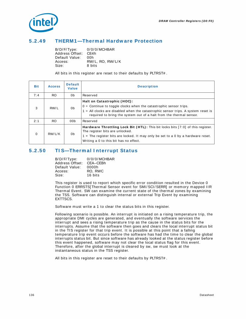
DRAM Controller Registers (D0:F0)
136 Datasheet
5.2.49 THERM1—Thermal Hardware Protection
B/D/F/Type: 0/0/0/MCHBARAddress Offset: CE4hDefault Value: 00hAccess: RW/L, RO, RW/L/K Size: 8 bits
All bits in this register are reset to their defaults by PLTRST#.
5.2.50 TIS—Thermal Interrupt Status
B/D/F/Type: 0/0/0/MCHBARAddress Offset: CEA–CEBhDefault Value: 0000hAccess: RO, RWC Size: 16 bits
This register is used to report which specific error condition resulted in the Device 0 Function 0 ERRSTS[Thermal Sensor event for SMI/SCI/SERR] or memory mapped IIR Thermal Event. SW can examine the current state of the thermal zones by examining the TSS. Software can distinguish internal or external Trip Event by examining EXTTSCS.
Software must write a 1 to clear the status bits in this register.
Following scenario is possible. An interrupt is initiated on a rising temperature trip, the appropriate DMI cycles are generated, and eventually the software services the interrupt and sees a rising temperature trip as the cause in the status bits for the interrupts. Assume that the software then goes and clears the local interrupt status bit in the TIS register for that trip event. It is possible at this point that a falling temperature trip event occurs before the software has had the time to clear the global interrupts status bit. But since software has already looked at the status register before this event happened, software may not clear the local status flag for this event. Therefore, after the global interrupt is cleared by sw, sw must look at the instantaneous status in the TSS register.
All bits in this register are reset to their defaults by PLTRST#.
Bit AccessDefault Value
Description
7:4 RO 0b Reserved
3 RW/L 0b
Halt on Catastrophic (HOC): 0 = Continue to toggle clocks when the catastrophic sensor trips.1 = All clocks are disabled when the catastrophic sensor trips. A system reset is
required to bring the system out of a halt from the thermal sensor.
2:1 RO 00b Reserved
0 RW/L/K 0b
Hardware Throttling Lock Bit (HTL): This bit locks bits [7:0] of this register. The register bits are unlocked.1 = The register bits are locked. It may only be set to a 0 by a hardware reset. Writing a 0 to this bit has no effect.

Datasheet 137
DRAM Controller Registers (D0:F0)
Bit AccessDefault Value
Description
15:10 RO 00h Reserved
9 RWC 0b
Was Catastrophic Thermal Sensor Interrupt Event (WCTSIE): 1 = Indicates that a Catastrophic Thermal Sensor trip based on a higher to lower
temperature transition thru the trip point 0 = No trip for this event
8 RWC 0b
Was Hot Thermal Sensor Interrupt Event (WHTSIE): 1 = Indicates that a Hot Thermal Sensor trip based on a higher to lower
temperature transition thru the trip point 0 = No trip for this event
7 RWC 0b
Was Aux0 Thermal Sensor Interrupt Event (WA0TSIE): 1 = Indicates that an Aux0 Thermal Sensor trip based on a higher to lower
temperature transition thru the trip point 0 = No trip for this event Software must write a 1 to clear this status bit.
6:5 RO 00b Reserved
4 RWC 0b
Catastrophic Thermal Sensor Interrupt Event (CTSIE): 1 = Indicates that a Catastrophic Thermal Sensor trip event occurred based on a
lower to higher temperature transition thru the trip point.0 = No trip for this event Software must write a 1 to clear this status bit.
3 RWC 0b
Hot Thermal Sensor Interrupt Event (HTSIE): 1 = Indicates that a Hot Thermal Sensor trip event occurred based on a lower to
higher temperature transition thru the trip point.0 = No trip for this event Software must write a 1 to clear this status bit.
2 RWC 0b
Aux0 Thermal Sensor Interrupt Event (A0TSIE): 1 = Indicates that an Aux0 Thermal Sensor trip event occurred based on a lower
to higher temperature transition thru the trip point. 0 = No trip for this event Software must write a 1 to clear this status bit.
1:0 RO 00b Reserved

DRAM Controller Registers (D0:F0)
138 Datasheet
5.2.51 TSMICMD—Thermal SMI Command
B/D/F/Type: 0/0/0/MCHBARAddress Offset: CF1hDefault Value: 00hAccess: RO, RW Size: 8 bits
This register selects specific errors to generate a SMI DMI special cycle, as enabled by the Device 0 SMI Error Command Register [SMI on MCH Thermal Sensor Trip]. The SMI must not be enabled at the same time as the SERR/SCI for the thermal sensor event.
All bits in this register are reset to their defaults by PLTRST#.
Bit AccessDefault Value
Description
7:3 RO 00h Reserved
2 RW 0b
SMI on MCH Catastrophic Thermal Sensor Trip (SMGCTST): 1 = Does not mask the generation of an SMI DMI special cycle on a catastrophic
thermal sensor trip.
0 = Disable reporting of this condition via SMI messaging.
1 RW 0b
SMI on MCH Hot Thermal Sensor Trip (SMGHTST): 1 = Does not mask the generation of an SMI DMI special cycle on a Hot thermal
sensor trip.0 = Disable reporting of this condition via SMI messaging.
0 RW 0b
SMI on MCH Aux Thermal Sensor Trip (SMGATST): 1 = Does not mask the generation of an SMI DMI special cycle on an Auxiliary
thermal sensor trip.0 = Disable reporting of this condition via SMI messaging.

Datasheet 139
DRAM Controller Registers (D0:F0)
5.2.52 PMSTS—Power Management Status
B/D/F/Type: 0/0/0/MCHBARAddress Offset: F14–F17hDefault Value: 00000000hAccess: RWC/S, RO Size: 32 bits
This register is Reset by PWROK only.
Bit AccessDefault Value
Description
31:9 RO 000000h Reserved
8 RWC/S 0b
Warm Reset Occurred (WRO): Set by the PMunit whenever a Warm Reset is received, and cleared by PWROK=0. 0 = No Warm Reset occurred.1 = Warm Reset occurred.BIOS Requirement: BIOS can check and clear this bit whenever executing POST code. This way BIOS knows that if the bit is set, then the PMSTS bits [1:0] must also be set, and if not BIOS needs to power-cycle the platform.
7:2 RO 00h Reserved
1 RWC/S 0b
Channel 1 in Self-Refresh (C1SR): Set by power management hardware after Channel 1 is placed in self refresh as a result of a Power State or a Reset Warn sequence.Cleared by Power management hardware before starting Channel 1 self refresh exit sequence initiated by a power management exit.Cleared by the BIOS by writing a "1" in a warm reset (Reset# asserted while PWROK is asserted) exit sequence.0 = Channel 1 not guaranteed to be in Self-Refresh.1 = Channel 1 in Self-Refresh.
0 RWC/S 0b
Channel 0 in Self-Refresh (C0SR): Set by power management hardware after Channel 0 is placed in self refresh as a result of a Power State or a Reset Warn sequence.Cleared by Power management hardware before starting Channel 0 self refresh exit sequence initiated by a power management exit.Cleared by the BIOS by writing a "1" in a warm reset (Reset# asserted while PWROK is asserted) exit sequence.0 = Channel 0 not guaranteed to be in Self-Refresh.1 = Channel 0 in Self-Refresh.
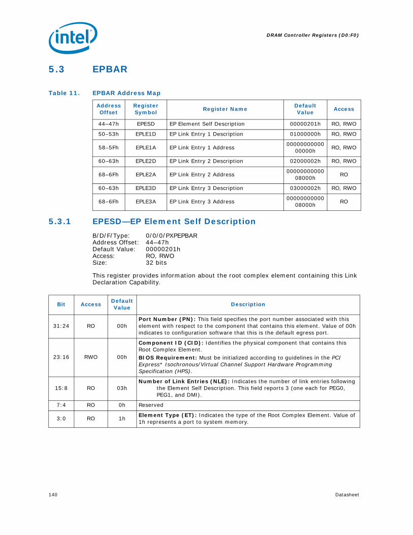
DRAM Controller Registers (D0:F0)
140 Datasheet
5.3 EPBAR
5.3.1 EPESD—EP Element Self Description
B/D/F/Type: 0/0/0/PXPEPBARAddress Offset: 44–47hDefault Value: 00000201hAccess: RO, RWO Size: 32 bits
This register provides information about the root complex element containing this Link Declaration Capability.
Table 11. EPBAR Address Map
Address Offset
Register Symbol
Register NameDefault Value
Access
44–47h EPESD EP Element Self Description 00000201h RO, RWO
50–53h EPLE1D EP Link Entry 1 Description 01000000h RO, RWO
58–5Fh EPLE1A EP Link Entry 1 Address00000000000
00000hRO, RWO
60–63h EPLE2D EP Link Entry 2 Description 02000002h RO, RWO
68–6Fh EPLE2A EP Link Entry 2 Address00000000000
08000hRO
60–63h EPLE3D EP Link Entry 3 Description 03000002h RO, RWO
68–6Fh EPLE3A EP Link Entry 3 Address00000000000
08000hRO
Bit AccessDefault Value
Description
31:24 RO 00hPort Number (PN): This field specifies the port number associated with this element with respect to the component that contains this element. Value of 00h indicates to configuration software that this is the default egress port.
23:16 RWO 00h
Component ID (CID): Identifies the physical component that contains this Root Complex Element.BIOS Requirement: Must be initialized according to guidelines in the PCI Express* Isochronous/Virtual Channel Support Hardware Programming Specification (HPS).
15:8 RO 03hNumber of Link Entries (NLE): Indicates the number of link entries following
the Element Self Description. This field reports 3 (one each for PEG0, PEG1, and DMI).
7:4 RO 0h Reserved
3:0 RO 1hElement Type (ET): Indicates the type of the Root Complex Element. Value of 1h represents a port to system memory.

Datasheet 141
DRAM Controller Registers (D0:F0)
5.3.2 EPLE1D—EP Link Entry 1 Description
B/D/F/Type: 0/0/0/PXPEPBARAddress Offset: 50–53hDefault Value: 01000000hAccess: RO, RWO Size: 32 bits
This register provides the first part of a Link Entry which declares an internal link to another Root Complex Element.
5.3.3 EPLE1A—EP Link Entry 1 Address
B/D/F/Type: 0/0/0/PXPEPBARAddress Offset: 58–5FhDefault Value: 0000000000000000hAccess: RO, RWO Size: 64 bits
This register provides the second part of a Link Entry which declares an internal link to another Root Complex Element.
Bit AccessDefault Value
Description
31:24 RO 01h
Target Port Number (TPN): Specifies the port number associated with the element targeted by this link entry (DMI). The target port number is with respect to the component that contains this element as specified by the target component ID.
23:16 RWO 00h
Target Component ID (TCID): Identifies the physical or logical component that is targeted by this link entry.BIOS Requirement: Must be initialized according to guidelines in the PCI Express* Isochronous/Virtual Channel Support Hardware Programming Specification (HPS).
15:2 RO 0000h Reserved
1 RO 0bLink Type (LTYP): Indicates that the link points to memory-mapped space (for RCRB). The link address specifies the 64-bit base address of the target RCRB.
0 RWO 0bLink Valid (LV): 0 = Link Entry is not valid and will be ignored.1 = Link Entry specifies a valid link.
Bit AccessDefault Value
Description
63:36 RO 0000000h Reserved
35:12 RWO 000000hLink Address (LA): Memory mapped base address of the RCRB that is the target element (DMI) for this link entry.
11:0 RO 000h Reserved

DRAM Controller Registers (D0:F0)
142 Datasheet
5.3.4 EPLE2D—EP Link Entry 2 Description
B/D/F/Type: 0/0/0/PXPEPBARAddress Offset: 60–63hDefault Value: 02000002hAccess: RO, RWO Size: 32 bits
This register provides the first part of a Link Entry which declares an internal link to another Root Complex Element.
5.3.5 EPLE2A—EP Link Entry 2 Address
B/D/F/Type: 0/0/0/PXPEPBARAddress Offset: 68–6FhDefault Value: 0000000000008000hAccess: RO Size: 64 bits
This register provides the second part of a Link Entry which declares an internal link to another Root Complex Element.
Bit AccessDefault Value
Description
31:24 RO 02h
Target Port Number (TPN): Specifies the port number associated with the element targeted by this link entry (PEG0). The target port number is with respect to the component that contains this element as specified by the target component ID.
23:16 RWO 00h
Target Component ID (TCID): Identifies the physical or logical component that is targeted by this link entry. A value of 0 is reserved. Component IDs start at 1. This value is a mirror of the value in the Component ID field of all elements in this component.
BIOS Requirement: Must be initialized according to guidelines in the PCI Express* Isochronous/Virtual Channel Support Hardware Programming Specification (HPS).
15:2 RO 0000h Reserved
1 RO 1b
Link Type (LTYP): Indicates that the link points to configuration space of the integrated device which controls the root port for PEG0.The link address specifies the configuration address (segment, bus, device, function) of the target root port.
0 RWO 0bLink Valid (LV): 0 = Link Entry is not valid and will be ignored.1 = Link Entry specifies a valid link.
Bit AccessDefault Value
Description
63:28 RO0000000
00hReserved
27:20 RO 00h Bus Number (BUSN):
19:15 RO 00001bDevice Number (DEVN): Target for this link is PCI Express port PEG0 (Device1).
14:12 RO 000b Function Number (FUNN):
11:0 RO 000h Reserved

Datasheet 143
DRAM Controller Registers (D0:F0)
5.3.6 EPLE3D—EP Link Entry 3 Description
B/D/F/Type: 0/0/0/PXPEPBARAddress Offset: 70–73hDefault Value: 03000002hAccess: RO, RWO Size: 32 bits
This register provides the first part of a Link Entry which declares an internal link to another Root Complex Element.
Bit AccessDefault Value
Description
31:24 RO 03h
Target Port Number (TPN): Specifies the port number associated with the element targeted by this link entry (PEG1). The target port number is with respect to the component that contains this element as specified by the target component ID.
23:16 RWO 00h
Target Component ID (TCID): Identifies the physical or logical component that is targeted by this link entry. A value of 0 is reserved. Component IDs start at 1. This value is a mirror of the value in the Component ID field of all elements in this component.BIOS Requirement: Must be initialized according to guidelines in the PCI Express* Isochronous/Virtual Channel Support Hardware Programming Specification (HPS).
15:2 RO 0000h Reserved
1 RO 1b
Link Type (LTYP): Indicates that the link points to configuration space of the integrated device which controls the root port for PEG1.The link address specifies the configuration address (segment, bus, device, function) of the target root port.
0 RWO 0bLink Valid (LV): 0 = Link Entry is not valid and will be ignored.1 = Link Entry specifies a valid link.
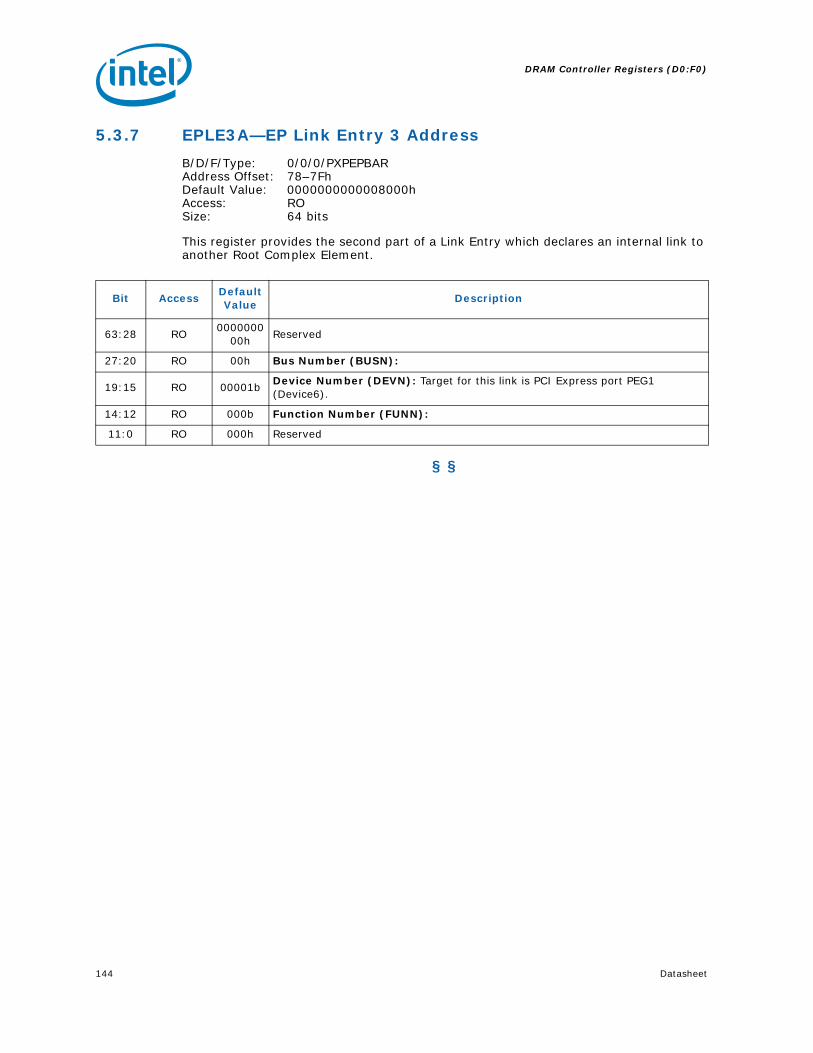
DRAM Controller Registers (D0:F0)
144 Datasheet
5.3.7 EPLE3A—EP Link Entry 3 Address
B/D/F/Type: 0/0/0/PXPEPBARAddress Offset: 78–7FhDefault Value: 0000000000008000hAccess: RO Size: 64 bits
This register provides the second part of a Link Entry which declares an internal link to another Root Complex Element.
§ §
Bit AccessDefault Value
Description
63:28 RO0000000
00hReserved
27:20 RO 00h Bus Number (BUSN):
19:15 RO 00001bDevice Number (DEVN): Target for this link is PCI Express port PEG1 (Device6).
14:12 RO 000b Function Number (FUNN):
11:0 RO 000h Reserved

Datasheet 145
Host-Primary PCI Express* Bridge Registers (D1:F0)
6 Host-Primary PCI Express* Bridge Registers (D1:F0)
Device 1 contains the controls associated with the PCI Express root port that is the intended attach point for external graphics. In addition, it also functions as the virtual PCI-to-PCI bridge. The table below provides an address map of the D1:F0 registers listed by address offset in ascending order. This chapter provides a detailed bit description of the registers.
Warning: When reading the PCI Express "conceptual" registers such as this, you may not get a valid value unless the register value is stable.
The PCI Express* Specification defines two types of reserved bits:
Reserved and Preserved:
• Reserved for future RW implementations; software must preserve value read for writes to bits.
• Reserved and Zero: Reserved for future R/WC/S implementations; software must use 0 for writes to bits.
Unless explicitly documented as Reserved and Zero, all bits marked as reserved are part of the Reserved and Preserved type, which have historically been the typical definition for Reserved.
Note: Most (if not all) control bits in this device cannot be modified unless the link is down. Software is required to first disable the link, then program the registers, and then re-enable the link (which will cause a full-retrain with the new settings).
Table 12. Host-PCI Express Bridge Register Address Map (D1:F0) (Sheet 1 of 3)
Address Offset
Register Symbol
Register NameDefault Value
Access
0–1h VID1 Vendor Identification 8086h RO
2–3h DID1 Device Identification 29E1h RO
4–5h PCICMD1 PCI Command 0000h RO, RW
6–7h PCISTS1 PCI Status 0010h RO, RWC
8h RID1 Revision Identification 00h RO
9–Bh CC1 Class Code 060400h RO
Ch CL1 Cache Line Size 00h RW
Eh HDR1 Header Type 01h RO
18h PBUSN1 Primary Bus Number 00h RO
19h SBUSN1 Secondary Bus Number 00h RW
1Ah SUBUSN1 Subordinate Bus Number 00h RW
1Ch IOBASE1 I/O Base Address F0h RO, RW
1Dh IOLIMIT1 I/O Limit Address 00h RW, RO
1E–1Fh SSTS1 Secondary Status 0000h RO, RWC
20–21h MBASE1 Memory Base Address FFF0h RW, RO

Host-Primary PCI Express* Bridge Registers (D1:F0)
146 Datasheet
22–23h MLIMIT1 Memory Limit Address 0000h RW, RO
24–25h PMBASE1 Prefetchable Memory Base Address FFF1h RW, RO
26–27h PMLIMIT1 Prefetchable Memory Limit Address 0001h RO, RW
28–2Bh PMBASEU1 Prefetchable Memory Base Address Upper 00000000h RW
2C–2Fh PMLIMITU1 Prefetchable Memory Limit Address Upper 00000000h RW
34h CAPPTR1 Capabilities Pointer 88h RO
3Ch INTRLINE1 Interrupt Line 00h RW
3Dh INTRPIN1 Interrupt Pin 01h RO
3E–3Fh BCTRL1 Bridge Control 0000h RO, RW
80–83h PM_CAPID1 Power Management Capabilities C8039001h RO
84–87h PM_CS1 Power Management Control/Status 00000008hRO, RW, RW/P
88–8Bh SS_CAPID Subsystem ID and Vendor ID Capabilities 0000800Dh RO
8C–8Fh SS Subsystem ID and Subsystem Vendor ID 00008086h RWO
90–91h MSI_CAPID Message Signaled Interrupts Capability ID A005h RO
92–93h MC Message Control 0000h RW, RO
94–97h MA Message Address 00000000h RO, RW
98–99h MD Message Data 0000h RW
A0–A1h PE_CAPL PCI Express Capability List 0010h RO
A2–A3h PE_CAP PCI Express Capabilities 0142h RO, RWO
A4–A7h DCAP Device Capabilities 00008000h RO
A8–A9h DCTL Device Control 0000h RW, RO
AA–ABh DSTS Device Status 0000h RO, RWC
AC–AFh LCAP Link Capabilities020214D02
hRO, RWO
B0–B1h LCTL Link Control 0000hRO, RW, RW/SC
B2–B3h LSTS Link Status 1000h RWC, RO
B4–B7h SLOTCAP Slot Capabilities 00040000h RWO, RO
B8–B9h SLOTCTL Slot Control 0000h RO, RW
BA–BBh SLOTSTS Slot Status 0000h RO, RWC
BC–BDh RCTL Root Control 0000h RO, RW
C0–C3h RSTS Root Status 00000000h RO, RWC
EC–EFh PELC PCI Express Legacy Control 00000000h RO, RW
100–103h VCECHVirtual Channel Enhanced Capability Header
14010002h RO
104–107h PVCCAP1 Port VC Capability Register 1 00000000h RO
108–10Bh PVCCAP2 Port VC Capability Register 2 00000000h RO
Table 12. Host-PCI Express Bridge Register Address Map (D1:F0) (Sheet 2 of 3)
Address Offset
Register Symbol
Register NameDefault Value
Access

Datasheet 147
Host-Primary PCI Express* Bridge Registers (D1:F0)
6.1 VID1—Vendor Identification
B/D/F/Type: 0/1/0/PCIAddress Offset: 0–1hDefault Value: 8086hAccess: RO Size: 16 bits
This register combined with the Device Identification register uniquely identify any PCI device.
10C–10Dh
PVCCTL Port VC Control 0000h RO, RW
110–113h VC0RCAP VC0 Resource Capability 00000001h RO
114–117h VC0RCTL VC0 Resource Control 800000FFh RO, RW
11A–11Bh VC0RSTS VC0 Resource Status 0002h RO
140–143h RCLDECH Root Complex Link Declaration Enhanced 00010005h RO
144–147h ESD Element Self Description 02000100h RO, RWO
150–153h LE1D Link Entry 1 Description 00000000h RO, RWO
158–15Fh LE1A Link Entry 1 Address0000000000000000h
RO, RWO
218–21Fh PESSTS PCI Express Sequence Status0000000000000FFFh
RO
Table 12. Host-PCI Express Bridge Register Address Map (D1:F0) (Sheet 3 of 3)
Address Offset
Register Symbol
Register NameDefault Value
Access
Bit AccessDefault Value
Description
15:0 RO 8086h Vendor Identification (VID1): PCI standard identification for Intel.

Host-Primary PCI Express* Bridge Registers (D1:F0)
148 Datasheet
6.2 DID1—Device Identification
B/D/F/Type: 0/1/0/PCIAddress Offset: 2–3hDefault Value: 29E1hAccess: RO Size: 16 bits
This register combined with the Vendor Identification register uniquely identifies any PCI device.
6.3 PCICMD1—PCI Command
B/D/F/Type: 0/1/0/PCIAddress Offset: 4–5hDefault Value: 0000hAccess: RO, RW Size: 16 bits
Bit AccessDefault Value
Description
15:8 RO 29hDevice Identification Number (DID1(UB)): Identifier assigned to the MCH device 1 (virtual PCI-to-PCI bridge, PCI Express port).
7:4 RO EhDevice Identification Number (DID1(HW)): Identifier assigned to the MCH device 1 (virtual PCI-to-PCI bridge, PCI Express port).
3:0 RO 1hDevice Identification Number (DID1(LB)): Identifier assigned to the MCH device 1 (virtual PCI-to-PCI bridge, PCI Express port).
Bit AccessDefault Value
Description
15:11 RO 00h Reserved
10 RW 0b
INTA Assertion Disable (INTAAD): 0 = This device is permitted to generate INTA interrupt messages.1 = This device is prevented from generating interrupt messages. Any INTA
emulation interrupts already asserted must be de-asserted when this bit is set.
Only affects interrupts generated by the device (PCI INTA from a PME event) controlled by this command register. It does not affect upstream MSIs, upstream PCI INTA-INTD assert and de-assert messages.
9 RO 0bFast Back-to-Back Enable (FB2B): Not Applicable or Implemented. Hardwired to 0.

Datasheet 149
Host-Primary PCI Express* Bridge Registers (D1:F0)
8 RW 0b
SERR# Message Enable (SERRE1): Controls Device 1 SERR# messaging. The MCH communicates the SERR# condition by sending an SERR message to the ICH. This bit, when set, enables reporting of non-fatal and fatal errors detected by the device to the Root Complex. Note that errors are reported if enabled either through this bit or through the PCI-Express specific bits in the Device Control Register.0 = The SERR message is generated by the MCH for Device 1 only under
conditions enabled individually through the Device Control Register.1 = The MCH is enabled to generate SERR messages which will be sent to the
ICH for specific Device 1 error conditions generated/detected on the primary side of the virtual PCI to PCI bridge (not those received by the secondary side). The status of SERRs generated is reported in the PCISTS1 register.
7 RO 0b Reserved
6 RW 0b
Parity Error Response Enable (PERRE): Controls whether or not the Master Data Parity Error bit in the PCI Status register can bet set.0 = Master Data Parity Error bit in PCI Status register can NOT be set.1 = Master Data Parity Error bit in PCI Status register CAN be set.
5:3 RO 0b Reserved
2 RW 0b
Bus Master Enable (BME): Controls the ability of the PCI Express port to forward Memory and IO Read/Write Requests in the upstream direction.0 = This device is prevented from making memory or IO requests to its primary
bus. Note that according to PCI Specification, as MSI interrupt messages are in-band memory writes, disabling the bus master enable bit prevents this device from generating MSI interrupt messages or passing them from its secondary bus to its primary bus. Upstream memory writes/reads, IO writes/reads, peer writes/reads, and MSIs will all be treated as illegal cycles. Writes are forwarded to memory address C0000h with byte enables de-asserted. Reads will be forwarded to memory address C0000h and will return Unsupported Request status (or Master abort) in its completion packet.
1 = This device is allowed to issue requests to its primary bus. Completions for previously issued memory read requests on the primary bus will be issued when the data is available.
This bit does not affect forwarding of Completions from the primary interface to the secondary interface.
1 RW 0b
Memory Access Enable (MAE): 0 = All of device 1's memory space is disabled.1 = Enable the Memory and Pre-fetchable memory address ranges defined in the
MBASE1, MLIMIT1, PMBASE1, and PMLIMIT1 registers.
0 RW 0b
I/O Access Enable (IOAE): 0 = All of device 1's I/O space is disabled.1 = Enable the I/O address range defined in the IOBASE1, and IOLIMIT1
registers.
Bit AccessDefault Value
Description

Host-Primary PCI Express* Bridge Registers (D1:F0)
150 Datasheet
6.4 PCISTS1—PCI Status
B/D/F/Type: 0/1/0/PCIAddress Offset: 6–7hDefault Value: 0010hAccess: RO, RWC Size: 16 bits
This register reports the occurrence of error conditions associated with primary side of the "virtual" Host-PCI Express bridge embedded within the MCH.
Bit AccessDefault Value
Description
15 RO 0bDetected Parity Error (DPE): Not Applicable or Implemented. Hardwired to 0. Parity (generating poisoned Transaction Layer Packets) is not supported on the primary side of this device.
14 RWC 0b
Signaled System Error (SSE): This bit is set when this Device sends an SERR due to detecting an ERR_FATAL or ERR_NONFATAL condition and the SERR Enable bit in the Command register is 1. Both received (if enabled by BCTRL1[1]) and internally detected error messages do not affect this field.
13 RO 0bReceived Master Abort Status (RMAS): Not Applicable or Implemented. Hardwired to 0. The concept of a master abort does not exist on primary side of this device.
12 RO 0bReceived Target Abort Status (RTAS): Not Applicable or Implemented. Hardwired to 0. The concept of a target abort does not exist on primary side of this device.
11 RO 0bSignaled Target Abort Status (STAS): Not Applicable or Implemented. Hardwired to 0. The concept of a target abort does not exist on primary side of this device.
10:9 RO 00bDEVSELB Timing (DEVT): This device is not the subtractively decoded device on bus 0. This bit field is therefore hardwired to 00 to indicate that the device uses the fastest possible decode.
8 RO 0b
Master Data Parity Error (PMDPE): Because the primary side of the PCI Express's virtual peer-to-peer bridge is integrated with the MCH functionality, there is no scenario where this bit will get set. Because hardware will never set this bit, it is impossible for software to have an opportunity to clear this bit or otherwise test that it is implemented. The PCI specification defines it as a R/WC, but for our implementation an RO definition behaves the same way and will meet all Microsoft testing requirements. This bit can only be set when the Parity Error Enable bit in the PCI Command register is set.
7 RO 0b Fast Back-to-Back (FB2B): Not Applicable or Implemented. Hardwired to 0.
6 RO 0b Reserved
5 RO 0b66/60MHz capability (CAP66): Not Applicable or Implemented. Hardwired to 0.
4 RO 1bCapabilities List (CAPL): Indicates that a capabilities list is present. Hardwired to 1.
3 RO 0b
INTA Status (INTAS): Indicates that an interrupt message is pending internally to the device. Only PME sources feed into this status bit (not PCI INTA-INTD assert and de-assert messages). The INTA Assertion Disable bit, PCICMD1[10], has no effect on this bit.
2:0 RO 000b Reserved

Datasheet 151
Host-Primary PCI Express* Bridge Registers (D1:F0)
6.5 RID1—Revision Identification
B/D/F/Type: 0/1/0/PCIAddress Offset: 8hDefault Value: see table belowAccess: RO Size: 8 bits
This register contains the revision number of the MCH device 1. These bits are read only and writes to this register have no effect.
6.6 CC1—Class Code
B/D/F/Type: 0/1/0/PCIAddress Offset: 9–BhDefault Value: 060400hAccess: RO Size: 24 bits
This register identifies the basic function of the device, a more specific sub-class, and a register-specific programming interface.
Bit AccessDefault Value
Description
7:0 ROsee
description
Revision Identification Number (RID1): This is an 8-bit value that indicates the revision identification number for the MCH Device 0. Refer to the Intel® X38 PCI Express Chipset Specification Update for the value of this register. Refer to the Intel® X38 Express Chipset Specification Update for the value of this register.
Bit AccessDefault Value
Description
23:16 RO 06hBase Class Code (BCC): Indicates the base class code for this device. This code has the value 06h, indicating a Bridge device.
15:8 RO 04hSub-Class Code (SUBCC): Indicates the sub-class code for this device. The code is 04h indicating a PCI to PCI Bridge.
7:0 RO 00hProgramming Interface (PI): Indicates the programming interface of this device. This value does not specify a particular register set layout and provides no practical use for this device.

Host-Primary PCI Express* Bridge Registers (D1:F0)
152 Datasheet
6.7 CL1—Cache Line Size
B/D/F/Type: 0/1/0/PCIAddress Offset: ChDefault Value: 00hAccess: RW Size: 8 bits
6.8 HDR1—Header Type
B/D/F/Type: 0/1/0/PCIAddress Offset: EhDefault Value: 01hAccess: RO Size: 8 bits
This register identifies the header layout of the configuration space. No physical register exists at this location.
6.9 PBUSN1—Primary Bus Number
B/D/F/Type: 0/1/0/PCIAddress Offset: 18hDefault Value: 00hAccess: RO Size: 8 bits
This register identifies that this "virtual" Host-PCI Express bridge is connected to PCI bus 0.
Bit AccessDefault Value
Description
7:0 RW 00hCache Line Size (Scratch pad): Implemented by PCI Express devices as a read-write field for legacy compatibility purposes but has no impact on any PCI Express device functionality.
Bit AccessDefault Value
Description
7:0 RO 01hHeader Type Register (HDR): Returns 01h to indicate that this is a single function device with bridge header layout.
Bit AccessDefault Value
Description
7:0 RO 00h
Primary Bus Number (BUSN): Configuration software typically programs this field with the number of the bus on the primary side of the bridge. Since device 1 is an internal device and its primary bus is always 0, these bits are read only and are hardwired to 0.

Datasheet 153
Host-Primary PCI Express* Bridge Registers (D1:F0)
6.10 SBUSN1—Secondary Bus Number
B/D/F/Type: 0/1/0/PCIAddress Offset: 19hDefault Value: 00hAccess: RW Size: 8 bits
This register identifies the bus number assigned to the second bus side of the "virtual" bridge. This number is programmed by the PCI configuration software to allow mapping of configuration cycles to PCI Express.
6.11 SUBUSN1—Subordinate Bus Number
B/D/F/Type: 0/1/0/PCIAddress Offset: 1AhDefault Value: 00hAccess: RW Size: 8 bits
This register identifies the subordinate bus (if any) that resides at the level below PCI Express. This number is programmed by the PCI configuration software to allow mapping of configuration cycles to PCI Express.
Bit AccessDefault Value
Description
7:0 RW 00hSecondary Bus Number (BUSN): This field is programmed by configuration software with the bus number assigned to PCI Express.
Bit AccessDefault Value
Description
7:0 RW 00h
Subordinate Bus Number (BUSN): This register is programmed by configuration software with the number of the highest subordinate bus that lies behind the device 1 bridge. When only a single PCI device resides on the PCI Express segment, this register will contain the same value as the SBUSN1 register.

Host-Primary PCI Express* Bridge Registers (D1:F0)
154 Datasheet
6.12 IOBASE1—I/O Base Address
B/D/F/Type: 0/1/0/PCIAddress Offset: 1ChDefault Value: F0hAccess: RO, RW Size: 8 bits
This register controls the processor to PCI Express I/O access routing based on the following formula:
IO_BASE ≤ address ≤ IO_LIMIT
Only upper 4 bits are programmable. For the purpose of address decode address bits A[11:0] are treated as 0. Thus the bottom of the defined I/O address range will be aligned to a 4 KB boundary.
6.13 IOLIMIT1—I/O Limit Address
B/D/F/Type: 0/1/0/PCIAddress Offset: 1DhDefault Value: 00hAccess: RW, RO Size: 8 bits
This register controls the processor to PCI Express I/O access routing based on the following formula:
IO_BASE ≤ address ≤ IO_LIMIT
Only upper 4 bits are programmable. For the purpose of address decode, address bits A[11:0] are assumed to be FFFh. Thus, the top of the defined I/O address range will be at the top of a 4 KB aligned address block.
Bit AccessDefault Value
Description
7:4 RW FhI/O Address Base (IOBASE): Corresponds to A[15:12] of the I/O addresses passed by bridge 1 to PCI Express.
3:0 RO 0h Reserved
Bit AccessDefault Value
Description
7:4 RW 0hI/O Address Limit (IOLIMIT): Corresponds to A[15:12] of the I/O address limit of device #1. Devices between this upper limit and IOBASE1 will be passed to the PCI Express hierarchy associated with this device.
3:0 RO 0h Reserved

Datasheet 155
Host-Primary PCI Express* Bridge Registers (D1:F0)
6.14 SSTS1—Secondary Status
B/D/F/Type: 0/1/0/PCIAddress Offset: 1E–1FhDefault Value: 0000hAccess: RO, RWC Size: 16 bits
SSTS1 is a 16-bit status register that reports the occurrence of error conditions associated with secondary side of the "virtual" PCI-PCI bridge embedded within MCH.
Bit AccessDefault Value
Description
15 RWC 0b
Detected Parity Error (DPE): This bit is set by the Secondary Side for a Type 1 Configuration Space header device whenever it receives a Poisoned Transaction Layer Packet, regardless of the state of the Parity Error Response Enable bit in the Bridge Control Register.
14 RWC 0bReceived System Error (RSE): This bit is set when the Secondary Side for a Type 1 configuration space header device receives an ERR_FATAL or ERR_NONFATAL.
13 RWC 0b
Received Master Abort (RMA): This bit is set when the Secondary Side for Type 1 Configuration Space Header Device (for requests initiated by the Type 1 Header Device itself) receives a Completion with Unsupported Request Completion Status.
12 RWC 0b
Received Target Abort (RTA): This bit is set when the Secondary Side for Type 1 Configuration Space Header Device (for requests initiated by the Type 1 Header Device itself) receives a Completion with Completer Abort Completion Status.
11 RO 0bSignaled Target Abort (STA): Not Applicable or Implemented. Hardwired to 0. The MCH does not generate Target Aborts (the MCH will never complete a request using the Completer Abort Completion status).
10:9 RO 00b DEVSELB Timing (DEVT): Not Applicable or Implemented. Hardwired to 0.
8 RWC 0b
Master Data Parity Error (SMDPE): When set indicates that the MCH received across the link (upstream) a Read Data Completion Poisoned Transaction Layer Packet (EP=1). This bit can only be set when the Parity Error Enable bit in the Bridge Control register is set.
7 RO 0b Fast Back-to-Back (FB2B): Not Applicable or Implemented. Hardwired to 0.
6 RO 0b Reserved
5 RO 0b66/60 MHz capability (CAP66): Not Applicable or Implemented. Hardwired to 0.
4:0 RO 00h Reserved
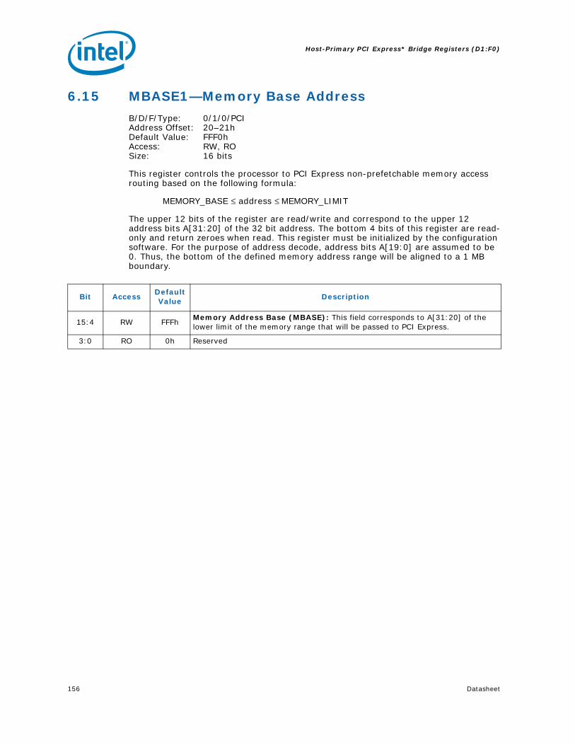
Host-Primary PCI Express* Bridge Registers (D1:F0)
156 Datasheet
6.15 MBASE1—Memory Base Address
B/D/F/Type: 0/1/0/PCIAddress Offset: 20–21hDefault Value: FFF0hAccess: RW, RO Size: 16 bits
This register controls the processor to PCI Express non-prefetchable memory access routing based on the following formula:
MEMORY_BASE ≤ address ≤ MEMORY_LIMIT
The upper 12 bits of the register are read/write and correspond to the upper 12 address bits A[31:20] of the 32 bit address. The bottom 4 bits of this register are read-only and return zeroes when read. This register must be initialized by the configuration software. For the purpose of address decode, address bits A[19:0] are assumed to be 0. Thus, the bottom of the defined memory address range will be aligned to a 1 MB boundary.
Bit AccessDefault Value
Description
15:4 RW FFFhMemory Address Base (MBASE): This field corresponds to A[31:20] of the lower limit of the memory range that will be passed to PCI Express.
3:0 RO 0h Reserved

Datasheet 157
Host-Primary PCI Express* Bridge Registers (D1:F0)
6.16 MLIMIT1—Memory Limit Address
B/D/F/Type: 0/1/0/PCIAddress Offset: 22–23hDefault Value: 0000hAccess: RW, RO Size: 16 bits
This register controls the processor to PCI Express non-prefetchable memory access routing based on the following formula:
MEMORY_BASE ≤ address ≤ MEMORY_LIMIT
The upper 12 bits of the register are read/write and correspond to the upper 12 address bits A[31:20] of the 32 bit address. The bottom 4 bits of this register are read-only and return zeroes when read. This register must be initialized by the configuration software. For the purpose of address decode address bits A[19:0] are assumed to be FFFFFh. Thus, the top of the defined memory address range will be at the top of a 1 MB aligned memory block.
Note: Memory range covered by MBASE and MLIMIT registers are used to map non-prefetchable PCI Express address ranges (typically where control/status memory-mapped I/O data structures of the controller will reside) and PMBASE and PMLIMIT are used to map prefetchable address ranges (typically device local memory). This segregation allows application of USWC space attribute to be performed in a true plug-and-play manner to the prefetchable address range for improved processor- PCI Express memory access performance.
Note: Configuration software is responsible for programming all address range registers (prefetchable, non-prefetchable) with the values that provide exclusive address ranges (i.e., prevent overlap with each other and/or with the ranges covered with the main memory). There is no provision in the MCH hardware to enforce prevention of overlap and operations of the system in the case of overlap are not ensured.
Bit AccessDefault Value
Description
15:4 RW 000hMemory Address Limit (MLIMIT): This field corresponds to A[31:20] of the upper limit of the address range passed to PCI Express.
3:0 RO 0h Reserved

Host-Primary PCI Express* Bridge Registers (D1:F0)
158 Datasheet
6.17 PMBASE1—Prefetchable Memory Base Address
B/D/F/Type: 0/1/0/PCIAddress Offset: 24–25hDefault Value: FFF1hAccess: RW, RO Size: 16 bits
This register in conjunction with the corresponding Upper Base Address register controls the processor to PCI Express prefetchable memory access routing based on the following formula:
PREFETCHABLE_MEMORY_BASE ≤ address ≤ PREFETCHABLE_MEMORY_LIMIT
The upper 12 bits of this register are read/write and correspond to address bits A[31:20] of the 40-bit address. The lower 8 bits of the Upper Base Address register are read/write and correspond to address bits A[39:32] of the 40-bit address. This register must be initialized by the configuration software. For the purpose of address decode, address bits A[19:0] are assumed to be 0. Thus, the bottom of the defined memory address range will be aligned to a 1MB boundary.
Bit AccessDefault Value
Description
15:4 RW FFFhPrefetchable Memory Base Address (MBASE): Corresponds to A[31:20] of the lower limit of the memory range that will be passed to PCI Express.
3:0 RO 1h64-bit Address Support: Indicates that the upper 32 bits of the prefetchable memory region base address are contained in the Prefetchable Memory base Upper Address register at 28h.
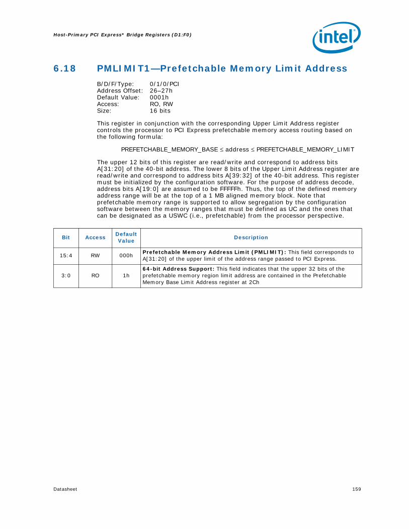
Datasheet 159
Host-Primary PCI Express* Bridge Registers (D1:F0)
6.18 PMLIMIT1—Prefetchable Memory Limit Address
B/D/F/Type: 0/1/0/PCIAddress Offset: 26–27hDefault Value: 0001hAccess: RO, RW Size: 16 bits
This register in conjunction with the corresponding Upper Limit Address register controls the processor to PCI Express prefetchable memory access routing based on the following formula:
PREFETCHABLE_MEMORY_BASE ≤ address ≤ PREFETCHABLE_MEMORY_LIMIT
The upper 12 bits of this register are read/write and correspond to address bits A[31:20] of the 40-bit address. The lower 8 bits of the Upper Limit Address register are read/write and correspond to address bits A[39:32] of the 40-bit address. This register must be initialized by the configuration software. For the purpose of address decode, address bits A[19:0] are assumed to be FFFFFh. Thus, the top of the defined memory address range will be at the top of a 1 MB aligned memory block. Note that prefetchable memory range is supported to allow segregation by the configuration software between the memory ranges that must be defined as UC and the ones that can be designated as a USWC (i.e., prefetchable) from the processor perspective.
Bit AccessDefault Value
Description
15:4 RW 000hPrefetchable Memory Address Limit (PMLIMIT): This field corresponds to A[31:20] of the upper limit of the address range passed to PCI Express.
3:0 RO 1h64-bit Address Support: This field indicates that the upper 32 bits of the prefetchable memory region limit address are contained in the Prefetchable Memory Base Limit Address register at 2Ch

Host-Primary PCI Express* Bridge Registers (D1:F0)
160 Datasheet
6.19 PMBASEU1—Prefetchable Memory Base Address Upper
B/D/F/Type: 0/1/0/PCIAddress Offset: 28–2BhDefault Value: 00000000hAccess: RW Size: 32 bits
The functionality associated with this register is present in the PCI Express design implementation.
This register in conjunction with the corresponding Upper Base Address register controls the processor to PCI Express prefetchable memory access routing based on the following formula:
PREFETCHABLE_MEMORY_BASE ≤ address ≤ PREFETCHABLE_MEMORY_LIMIT
The upper 12 bits of this register are read/write and correspond to address bits A[31:20] of the 40-bit address. The lower 8 bits of the Upper Base Address register are read/write and correspond to address bits A[39:32] of the 40-bit address. This register must be initialized by the configuration software. For the purpose of address decode, address bits A[19:0] are assumed to be 0. Thus, the bottom of the defined memory address range will be aligned to a 1MB boundary.
Bit AccessDefault Value
Description
31:0 RW0000000
0h
Prefetchable Memory Base Address (MBASEU): This field corresponds to A[63:32] of the lower limit of the prefetchable memory range that will be passed to PCI Express.
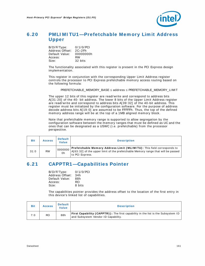
Datasheet 161
Host-Primary PCI Express* Bridge Registers (D1:F0)
6.20 PMLIMITU1—Prefetchable Memory Limit Address Upper
B/D/F/Type: 0/1/0/PCIAddress Offset: 2C–2FhDefault Value: 00000000hAccess: RW Size: 32 bits
The functionality associated with this register is present in the PCI Express design implementation.
This register in conjunction with the corresponding Upper Limit Address register controls the processor to PCI Express prefetchable memory access routing based on the following formula:
PREFETCHABLE_MEMORY_BASE ≤ address ≤ PREFETCHABLE_MEMORY_LIMIT
The upper 12 bits of this register are read/write and correspond to address bits A[31:20] of the 40- bit address. The lower 8 bits of the Upper Limit Address register are read/write and correspond to address bits A[39:32] of the 40-bit address. This register must be initialized by the configuration software. For the purpose of address decode address bits A[19:0] are assumed to be FFFFFh. Thus, the top of the defined memory address range will be at the top of a 1MB aligned memory block.
Note that prefetchable memory range is supported to allow segregation by the configuration software between the memory ranges that must be defined as UC and the ones that can be designated as a USWC (i.e. prefetchable) from the processor perspective.
6.21 CAPPTR1—Capabilities Pointer
B/D/F/Type: 0/1/0/PCIAddress Offset: 34hDefault Value: 88hAccess: RO Size: 8 bits
The capabilities pointer provides the address offset to the location of the first entry in this device's linked list of capabilities.
Bit AccessDefault Value
Description
31:0 RW0000000
0h
Prefetchable Memory Address Limit (MLIMITU): This field corresponds to A[63:32] of the upper limit of the prefetchable Memory range that will be passed to PCI Express.
Bit AccessDefault Value
Description
7:0 RO 88hFirst Capability (CAPPTR1): The first capability in the list is the Subsystem ID and Subsystem Vendor ID Capability.
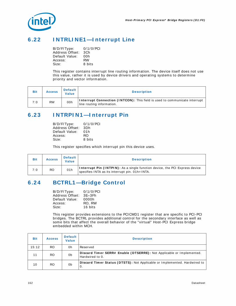
Host-Primary PCI Express* Bridge Registers (D1:F0)
162 Datasheet
6.22 INTRLINE1—Interrupt Line
B/D/F/Type: 0/1/0/PCIAddress Offset: 3ChDefault Value: 00hAccess: RW Size: 8 bits
This register contains interrupt line routing information. The device itself does not use this value, rather it is used by device drivers and operating systems to determine priority and vector information.
6.23 INTRPIN1—Interrupt Pin
B/D/F/Type: 0/1/0/PCIAddress Offset: 3DhDefault Value: 01hAccess: RO Size: 8 bits
This register specifies which interrupt pin this device uses.
6.24 BCTRL1—Bridge Control
B/D/F/Type: 0/1/0/PCIAddress Offset: 3E–3FhDefault Value: 0000hAccess: RO, RW Size: 16 bits
This register provides extensions to the PCICMD1 register that are specific to PCI-PCI bridges. The BCTRL provides additional control for the secondary interface as well as some bits that affect the overall behavior of the "virtual" Host-PCI Express bridge embedded within MCH.
Bit AccessDefault Value
Description
7:0 RW 00hInterrupt Connection (INTCON): This field is used to communicate interrupt line routing information.
Bit AccessDefault Value
Description
7:0 RO 01hInterrupt Pin (INTPIN): As a single function device, the PCI Express device specifies INTA as its interrupt pin. 01h=INTA.
Bit AccessDefault Value
Description
15:12 RO 0h Reserved
11 RO 0bDiscard Timer SERR# Enable (DTSERRE): Not Applicable or Implemented. Hardwired to 0.
10 RO 0bDiscard Timer Status (DTSTS): Not Applicable or Implemented. Hardwired to 0.

Datasheet 163
Host-Primary PCI Express* Bridge Registers (D1:F0)
9 RO 0bSecondary Discard Timer (SDT): Not Applicable or Implemented. Hardwired to 0.
8 RO 0bPrimary Discard Timer (PDT): Not Applicable or Implemented. Hardwired to 0.
7 RO 0bFast Back-to-Back Enable (FB2BEN): Not Applicable or Implemented. Hardwired to 0.
6 RW 0bSecondary Bus Reset (SRESET): Setting this bit triggers a hot reset on the corresponding PCI Express Port. This will force the LTSSM to transition to the Hot Reset state (via Recovery) from L0, L0s, or L1 states.
5 RO 0bMaster Abort Mode (MAMODE): Does not apply to PCI Express. Hardwired to 0.
4 RW 0b
VGA 16-bit Decode (VGA16D): Enables the PCI-to-PCI bridge to provide 16-bit decoding of VGA I/O address precluding the decoding of alias addresses every 1 KB. This bit only has meaning if bit 3 (VGA Enable) of this register is also set to 1, enabling VGA I/O decoding and forwarding by the bridge.0 = Execute 10-bit address decodes on VGA I/O accesses.1 = Execute 16-bit address decodes on VGA I/O accesses.
3 RW 0bVGA Enable (VGAEN): Controls the routing of processor initiated transactions targeting VGA compatible I/O and memory address ranges. See the VGAEN/MDAP table in device 0, offset 97h[0].
2 RW 0b
ISA Enable (ISAEN): Needed to exclude legacy resource decode to route ISA resources to legacy decode path. Modifies the response by the MCH to an I/O access issued by the processor that target ISA I/O addresses. This applies only to I/O addresses that are enabled by the IOBASE and IOLIMIT registers. 0 = All addresses defined by the IOBASE and IOLIMIT for processor I/O
transactions will be mapped to PCI Express. 1 = MCH will not forward to PCI Express any I/O transactions addressing the last
768 bytes in each 1KB block even if the addresses are within the range defined by the IOBASE and IOLIMIT registers.
1 RW 0b
SERR Enable (SERREN): 0 = No forwarding of error messages from secondary side to primary side that
could result in an SERR.1 = ERR_COR, ERR_NONFATAL, and ERR_FATAL messages result in SERR
message when individually enabled by the Root Control register.
0 RW 0b
Parity Error Response Enable (PEREN): Controls whether or not the Master Data Parity Error bit in the Secondary Status register is set when the MCH receives across the link (upstream) a Read Data Completion Poisoned Transaction Layer Packet.0 = Master Data Parity Error bit in Secondary Status register can NOT be set.1 = Master Data Parity Error bit in Secondary Status register CAN be set.
Bit AccessDefault Value
Description

Host-Primary PCI Express* Bridge Registers (D1:F0)
164 Datasheet
6.25 PM_CAPID1—Power Management Capabilities
B/D/F/Type: 0/1/0/PCIAddress Offset: 80–83hDefault Value: C8039001hAccess: RO Size: 32 bits
Bit AccessDefault Value
Description
31:27 RO 19h
PME Support (PMES): This field indicates the power states in which this device may indicate PME wake via PCI Express messaging. D0, D3hot & D3cold. This device is not required to do anything to support D3hot & D3cold, it simply must report that those states are supported. Refer to the PCI Power Management 1.1 specification for encoding explanation and other power management details.
26 RO 0bD2 Power State Support (D2PSS): Hardwired to 0 to indicate that the D2 power management state is NOT supported.
25 RO 0bD1 Power State Support (D1PSS): Hardwired to 0 to indicate that the D1 power management state is NOT supported.
24:22 RO 000bAuxiliary Current (AUXC): Hardwired to 0 to indicate that there are no 3.3Vaux auxiliary current requirements.
21 RO 0bDevice Specific Initialization (DSI): Hardwired to 0 to indicate that special initialization of this device is NOT required before generic class device driver is to use it.
20 RO 0b Auxiliary Power Source (APS): Hardwired to 0.
19 RO 0bPME Clock (PMECLK): Hardwired to 0 to indicate this device does NOT support PMEB generation.
18:16 RO 011bPCI PM CAP Version (PCIPMCV): A value of 011b indicates that this function complies with revision 1.2 of the PCI Power Management Interface Specification.
15:8 RO 90hPointer to Next Capability (PNC): This contains a pointer to the next item in the capabilities list. If MSICH (CAPL[0] @ 7Fh) is 0, then the next item in the capabilities list is the Message Signaled Interrupts (MSI) capability at 90h.
7:0 RO 01hCapability ID (CID): Value of 01h identifies this linked list item (capability structure) as being for PCI Power Management registers.

Datasheet 165
Host-Primary PCI Express* Bridge Registers (D1:F0)
6.26 PM_CS1—Power Management Control/Status
B/D/F/Type: 0/1/0/PCIAddress Offset: 84–87hDefault Value: 00000008hAccess: RO, RW, RW/P Size: 32 bits
Bit AccessDefault Value
Description
31:16 RO 0000h Reserved
15 RO 0bPME Status (PMESTS): Indicates that this device does not support PMEB generation from D3cold.
14:13 RO 00bData Scale (DSCALE): Indicates that this device does not support the power management data register.
12:9 RO 0hData Select (DSEL): Indicates that this device does not support the power management data register.
8 RW/P 0b
PME Enable (PMEE): Indicates that this device does not generate PMEB assertion from any D-state.0 = PMEB generation not possible from any D State1 = PMEB generation enabled from any D StateThe setting of this bit has no effect on hardware.See PM_CAP[15:11]
7:2 RO 0000b Reserved
1:0 RW 00b
Power State (PS): Indicates the current power state of this device and can be used to set the device into a new power state. If software attempts to write an unsupported state to this field, write operation must complete normally on the bus, but the data is discarded and no state change occurs.00 = D011 = D3Support of D3cold does not require any special action. While in the D3hot state, this device can only act as the target of PCI configuration transactions (for power management control). This device also cannot generate interrupts or respond to MMR cycles in the D3 state. The device must return to the D0 state in order to be fully-functional. When the Power State is other than D0, the bridge will Master Abort (i.e. not claim) any downstream cycles (with exception of type 0 configuration cycles). Consequently, these unclaimed cycles will go down DMI and come back up as Unsupported Requests, which the MCH logs as Master Aborts in Device 0 PCISTS[13]There is no additional hardware functionality required to support these Power States.

Host-Primary PCI Express* Bridge Registers (D1:F0)
166 Datasheet
6.27 SS_CAPID—Subsystem ID and Vendor ID Capabilities
B/D/F/Type: 0/1/0/PCIAddress Offset: 88–8BhDefault Value: 0000800DhAccess: RO Size: 32 bits
This capability is used to uniquely identify the subsystem where the PCI device resides. Because this device is an integrated part of the system and not an add-in device, it is anticipated that this capability will never be used. However, it is necessary because Microsoft will test for its presence.
6.28 SS—Subsystem ID and Subsystem Vendor ID
B/D/F/Type: 0/1/0/PCIAddress Offset: 8C–8FhDefault Value: 00008086hAccess: RWO Size: 32 bits
System BIOS can be used as the mechanism for loading the SSID/SVID values. These values must be preserved through power management transitions and a hardware reset.
Bit AccessDefault Value
Description
31:16 RO 0000h Reserved
15:8 RO 80hPointer to Next Capability (PNC): This contains a pointer to the next item in the capabilities list which is the PCI Power Management capability.
7:0 RO 0DhCapability ID (CID): Value of 0Dh identifies this linked list item (capability structure) as being for SSID/SSVID registers in a PCI-to-PCI Bridge.
Bit AccessDefault Value
Description
31:16 RWO 0000hSubsystem ID (SSID): Identifies the particular subsystem and is assigned by the vendor.
15:0 RWO 8086hSubsystem Vendor ID (SSVID): Identifies the manufacturer of the subsystem and is the same as the vendor ID which is assigned by the PCI Special Interest Group.

Datasheet 167
Host-Primary PCI Express* Bridge Registers (D1:F0)
6.29 MSI_CAPID—Message Signaled Interrupts Capability ID
B/D/F/Type: 0/1/0/PCIAddress Offset: 90–91hDefault Value: A005hAccess: RO Size: 16 bits
When a device supports MSI, it can generate an interrupt request to the processor by writing a predefined data item (a message) to a predefined memory address.
6.30 MC—Message Control
B/D/F/Type: 0/1/0/PCIAddress Offset: 92–93hDefault Value: 0000hAccess: RW, RO Size: 16 bits
System software can modify bits in this register, but the device is prohibited from doing so.
If the device writes the same message multiple times, only one of those messages is ensured to be serviced. If all of them must be serviced, the device must not generate the same message again until the driver services the earlier one.
Bit AccessDefault Value
Description
15:8 RO A0hPointer to Next Capability (PNC): This contains a pointer to the next item in the capabilities list which is the PCI Express capability.
7:0 RO 05hCapability ID (CID): Value of 05h identifies this linked list item (capability structure) as being for MSI registers.
Bit AccessDefault Value
Description
15:8 RO 00h Reserved
7 RO 0b64-bit Address Capable (64AC): Hardwired to 0 to indicate that the function does not implement the upper 32 bits of the Message Address register and is incapable of generating a 64-bit memory address.
6:4 RW 000b
Multiple Message Enable (MME): System software programs this field to indicate the actual number of messages allocated to this device. This number will be equal to or less than the number actually requested. The encoding is the same as for the MMC field below.
3:1 RO 000b
Multiple Message Capable (MMC): System software reads this field to determine the number of messages being requested by this device. The value of 000b equates to 1 message requested.000 = 1 message requestedAll other encodings are reserved.
0 RW 0b
MSI Enable (MSIEN): Controls the ability of this device to generate MSIs. 0 = 0MSI will not be generated. 1 = MSI will be generated when we receive PME messages. INTA will not be
generated and INTA Status (PCISTS1[3]) will not be set.

Host-Primary PCI Express* Bridge Registers (D1:F0)
168 Datasheet
6.31 MA—Message Address
B/D/F/Type: 0/1/0/PCIAddress Offset: 94–97hDefault Value: 00000000hAccess: RO, RW Size: 32 bits
6.32 MD—Message Data
B/D/F/Type: 0/1/0/PCIAddress Offset: 98–99hDefault Value: 0000hAccess: RW Size: 16 bits
6.33 PE_CAPL—PCI Express* Capability List
B/D/F/Type: 0/1/0/PCIAddress Offset: A0–A1hDefault Value: 0010hAccess: RO Size: 16 bits
This register enumerates the PCI Express capability structure.
Bit AccessDefault Value
Description
31:2 RW0000000
0h
Message Address (MA): Used by system software to assign an MSI address to the device. The device handles an MSI by writing the padded contents of the MD register to this address.
1:0 RO 00bForce DWord Align (FDWA): Hardwired to 0 so that addresses assigned by system software are always aligned on a dword address boundary.
Bit AccessDefault Value
Description
15:0 RW 0000h
Message Data (MD): Base message data pattern assigned by system software and used to handle an MSI from the device. When the device must generate an interrupt request, it writes a 32-bit value to the memory address specified in the MA register. The upper 16-bits are always set to 0. The lower 16-bits are supplied by this register.
Bit AccessDefault Value
Description
15:8 RO 00h
Pointer to Next Capability (PNC): This value terminates the capabilities list. The Virtual Channel capability and any other PCI Express specific capabilities that are reported via this mechanism are in a separate capabilities list located entirely within PCI Express Extended Configuration Space.
7:0 RO 10hCapability ID (CID): Identifies this linked list item (capability structure) as being for PCI Express registers.

Datasheet 169
Host-Primary PCI Express* Bridge Registers (D1:F0)
6.34 PE_CAP—PCI Express* Capabilities
B/D/F/Type: 0/1/0/PCIAddress Offset: A2–A3hDefault Value: 0142hAccess: RO, RWO Size: 16 bits
This register indicates PCI Express device capabilities.
6.35 DCAP—Device Capabilities
B/D/F/Type: 0/1/0/PCIAddress Offset: A4–A7hDefault Value: 00008000hAccess: RO Size: 32 bits
This register indicates PCI Express device capabilities.
Bit AccessDefault Value
Description
15:14 RO 00b Reserved
13:9 RO 00hInterrupt Message Number (IMN): Not Applicable or Implemented. Hardwired to 0.
8 RWO 1b
Slot Implemented (SI): 0 = The PCI Express Link associated with this port is connected to an integrated
component or is disabled.1 = The PCI Express Link associated with this port is connected to a slot.
7:4 RO 4hDevice/Port Type (DPT): Hardwired to 4h to indicate root port of PCI Express Root Complex.
3:0 RO 2hPCI Express Capability Version (PCIECV): Hardwired to 2h to indicate compliance to the PCI Express Capabilities Register Expansion ECN.
Bit AccessDefault Value
Description
31:16 RO 0000h Reserved
15 RO 1bRole Based Error Reporting (RBER): Role Based Error Reporting (RBER): Indicates that this device implements the functionality defined in the Error Reporting ECN as required by the PCI Express 1.1 spec.
14:6 RO 000h Reserved
5 RO 0bExtended Tag Field Supported (ETFS): Hardwired to indicate support for 5-bit Tags as a Requestor.
4:3 RO 00bPhantom Functions Supported (PFS): Not Applicable or Implemented. Hardwired to 0.
2:0 RO 000bMax Payload Size (MPS): Hardwired to indicate 128B max supported payload for Transaction Layer Packets (TLP).

Host-Primary PCI Express* Bridge Registers (D1:F0)
170 Datasheet
6.36 DCTL—Device Control
B/D/F/Type: 0/1/0/PCIAddress Offset: A8–A9hDefault Value: 0000hAccess: RW, RO Size: 16 bits
This register provides control for PCI Express device specific capabilities.
The error reporting enable bits are in reference to errors detected by this device, not error messages received across the link. The reporting of error messages (ERR_CORR, ERR_NONFATAL, ERR_FATAL) received by Root Port is controlled exclusively by Root Port Command Register.
Bit AccessDefault Value
Description
15:8 RO 0h Reserved
7:5 RW 000b
Max Payload Size (MPS): 000 = 128B max supported payload for Transaction Layer Packets (TLP). As a
receiver, the Device must handle TLPs as large as the set value; as transmitter, the Device must not generate TLPs exceeding the set value.
All other encodings are reserved.Hardware will actually ignore this field. It is writeable only to support compliance testing.
4 RO 0b Reserved.
3 RW 0b
Unsupported Request Reporting Enable (URRE): When set, this bit allows signaling ERR_NONFATAL, ERR_FATAL, or ERR_CORR to the Root Control register when detecting an unmasked Unsupported Request (UR). An ERR_CORR is signaled when an unmasked Advisory Non-Fatal UR is received. An ERR_FATAL or ERR_NONFATAL is sent to the Root Control register when an uncorrectable non-Advisory UR is received with the severity bit set in the Uncorrectable Error Severity register.
2 RW 0b
Fatal Error Reporting Enable (FERE): When set, this bit enables signaling of ERR_FATAL to the Root Control register due to internally detected errors or error messages received across the link. Other bits also control the full scope of related error reporting.
1 RW 0b
Non-Fatal Error Reporting Enable (NERE): When set, this bit enables signaling of ERR_NONFATAL to the Rool Control register due to internally detected errors or error messages received across the link. Other bits also control the full scope of related error reporting.
0 RW 0b
Correctable Error Reporting Enable (CERE): When set, this bit enables signaling of ERR_CORR to the Root Control register due to internally detected errors or error messages received across the link. Other bits also control the full scope of related error reporting.

Datasheet 171
Host-Primary PCI Express* Bridge Registers (D1:F0)
6.37 DSTS—Device Status
B/D/F/Type: 0/1/0/PCIAddress Offset: AA–ABhDefault Value: 0000hAccess: RO, RWC Size: 16 bits
Reflects status corresponding to controls in the Device Control register. The error reporting bits are in reference to errors detected by this device, not errors messages received across the link.
Bit AccessDefault Value
Description
15:6 RO 000h Reserved
5 RO 0b
Transactions Pending (TP): 0 = All pending transactions (including completions for any outstanding non-
posted requests on any used virtual channel) have been completed.1 = Indicates that the device has transaction(s) pending (including completions
for any outstanding non-posted requests for all used Traffic Classes).
4 RO 0b Reserved
3 RWC 0b
Unsupported Request Detected (URD): When set, this bit indicates that the Device received an Unsupported Request. Errors are logged in this register regardless of whether error reporting is enabled or not in the Device Control Register.Additionally, the Non-Fatal Error Detected bit or the Fatal Error Detected bit is set according to the setting of the Unsupported Request Error Severity bit. In production systems setting the Fatal Error Detected bit is not an option as support for AER will not be reported.
2 RWC 0b
Fatal Error Detected (FED): When set, this bit indicates that fatal error(s) were detected. Errors are logged in this register regardless of whether error reporting is enabled or not in the Device Control register. When Advanced Error Handling is enabled, errors are logged in this register regardless of the settings of the uncorrectable error mask register.
1 RWC 0b
Non-Fatal Error Detected (NFED): When set, this bit indicates that non-fatal error(s) were detected. Errors are logged in this register regardless of whether error reporting is enabled or not in the Device Control register.When Advanced Error Handling is enabled, errors are logged in this register regardless of the settings of the uncorrectable error mask register.
0 RWC 0b
Correctable Error Detected (CED): When set, this bit indicates that correctable error(s) were detected. Errors are logged in this register regardless of whether error reporting is enabled or not in the Device Control register. When Advanced Error Handling is enabled, errors are logged in this register regardless of the settings of the correctable error mask register.
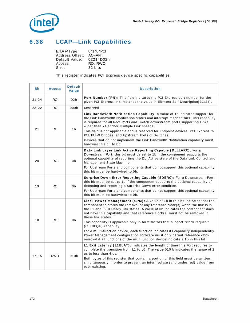
Host-Primary PCI Express* Bridge Registers (D1:F0)
172 Datasheet
6.38 LCAP—Link Capabilities
B/D/F/Type: 0/1/0/PCIAddress Offset: AC–AFhDefault Value: 02214D02hAccess: RO, RWO Size: 32 bits
This register indicates PCI Express device specific capabilities.
Bit AccessDefault Value
Description
31:24 RO 02hPort Number (PN): This field indicates the PCI Express port number for the given PCI Express link. Matches the value in Element Self Description[31:24].
23:22 RO 000b Reserved
21 RO 1b
Link Bandwidth Notification Capability: A value of 1b indicates support for the Link Bandwidth Notification status and interrupt mechanisms. This capability is required for all Root Ports and Switch downstream ports supporting Links wider than x1 and/or multiple Link speeds.
This field is not applicable and is reserved for Endpoint devices, PCI Express to PCI/PCI-X bridges, and Upstream Ports of Switches.Devices that do not implement the Link Bandwidth Notification capability must hardwire this bit to 0b.
20 RO 0b
Data Link Layer Link Active Reporting Capable (DLLLARC): For a Downstream Port, this bit must be set to 1b if the component supports the optional capability of reporting the DL_Active state of the Data Link Control and Management State Machine.For Upstream Ports and components that do not support this optional capability, this bit must be hardwired to 0b.
19 RO 0b
Surprise Down Error Reporting Capable (SDERC): For a Downstream Port, this bit must be set to 1b if the component supports the optional capability of detecting and reporting a Surprise Down error condition.For Upstream Ports and components that do not support this optional capability, this bit must be hardwired to 0b.
18 RO 0b
Clock Power Management (CPM): A value of 1b in this bit indicates that the component tolerates the removal of any reference clock(s) when the link is in the L1 and L2/3 Ready link states. A value of 0b indicates the component does not have this capability and that reference clock(s) must not be removed in these link states.This capability is applicable only in form factors that support "clock request" (CLKREQ#) capability.For a multi-function device, each function indicates its capability independently. Power Management configuration software must only permit reference clock removal if all functions of the multifunction device indicate a 1b in this bit.
17:15 RWO 010b
L1 Exit Latency (L1ELAT): Indicates the length of time this Port requires to complete the transition from L1 to L0. The value 010 b indicates the range of 2 us to less than 4 us.Both bytes of this register that contain a portion of this field must be written simultaneously in order to prevent an intermediate (and undesired) value from ever existing.

Datasheet 173
Host-Primary PCI Express* Bridge Registers (D1:F0)
14:12 RO 100b
L0s Exit Latency (L0SELAT): Indicates the length of time this Port requires to complete the transition from L0s to L0.000 = Less than 64 ns001 = 64 ns to less than 128 ns010 = 128 ns to less than 256 ns011 = 256 ns to less than 512 ns100 = 512 ns to less than 1 us101 = 1 us to less than 2 us110 = 2 us – 4 us111 = More than 4 usThe actual value of this field depends on the common Clock Configuration bit (LCTL[6])
11:10 RWO 11bActive State Link PM Support (ASLPMS): The MCH supports ASPM L0s and L1.
9:4 RO 10hMax Link Width (MLW): This field indicates the maximum number of lanes supported for this link.10h = x16
3:0 RWO 2h
Max Link Speed (MLS): Supported Link Speed - This field indicates the supported Link speed(s) of the associated Port.0001b = 2.5GT/s Link speed supported0010b = 5.0GT/s and 2.5GT/s Link speeds supportedAll other encodings are reserved.
Bit AccessDefault Value
Description

Host-Primary PCI Express* Bridge Registers (D1:F0)
174 Datasheet
6.39 LCTL—Link Control
B/D/F/Type: 0/1/0/PCIAddress Offset: B0–B1hDefault Value: 0000hAccess: RO, RW, RW/SC Size: 16 bits
This register allows control of PCI Express link.
Bit AccessDefault Value
Description
15:12 RO 0000b Reserved
11 RW 0b
Link Autonomous Bandwidth Interrupt Enable: When set, this bit enables the generation of an interrupt to indicate that the Link Autonomous Bandwidth Status bit has been set.This bit is not applicable and is reserved for Endpoint devices, PCI Express to PCI/PCI-X bridges, and Upstream Ports of Switches.Devices that do not implement the Link Bandwidth Notification capability must hardwire this bit to 0b.
10 RW 0b
Link Bandwidth Management Interrupt Enable: When set, this bit enables the generation of an interrupt to indicate that the Link Bandwidth Management Status bit has been set.This bit is not applicable and is reserved for Endpoint devices, PCI Express to PCI/PCI-X bridges, and Upstream Ports of Switches.
9 RO 0b
Hardware Autonomous Width Disable: When set, this bit disables hardware from changing the Link width for reasons other than attempting to correct unreliable Link operation by reducing Link width.Devices that do not implement the ability autonomously to change Link width are permitted to hardwire this bit to 0b.The MCH does not support autonomous width change. So, this bit is "RO".
8 RO 0b
Enable Clock Power Management (ECPM): Applicable only for form factors that support a "Clock Request" (CLKREQ#) mechanism, this enable functions as follows:0 = Clock power management is disabled and device must hold CLKREQ# signal
low1 = When this bit is set to 1 the device is permitted to use CLKREQ# signal to
power manage link clock according to protocol defined in appropriate form factor specification.
Default value of this field is 0b.Components that do not support Clock Power Management (as indicated by a 0b value in the Clock Power Management bit of the Link Capabilities Register) must hardwire this bit to 0b.
7 RW 0b
Extended Synch (ES): 0 = Standard Fast Training Sequence (FTS).1 = Forces the transmission of additional ordered sets when exiting the L0s state
and when in the Recovery state.This mode provides external devices (e.g., logic analyzers) monitoring the Link time to achieve bit and symbol lock before the link enters L0 and resumes communication.This is a test mode only and may cause other undesired side effects such as buffer overflows or underruns.

Datasheet 175
Host-Primary PCI Express* Bridge Registers (D1:F0)
6 RW 0b
Common Clock Configuration (CCC): 0 = Indicates that this component and the component at the opposite end of this
Link are operating with asynchronous reference clock.1 = Indicates that this component and the component at the opposite end of this
Link are operating with a distributed common reference clock.The state of this bit affects the L0s Exit Latency reported in LCAP[14:12] and the N_FTS value advertised during link training.
5 RW/SC 0b
Retrain Link (RL): 0 = Normal operation.1 = Full Link retraining is initiated by directing the Physical Layer LTSSM from
L0, L0s, or L1 states to the Recovery state.This bit always returns 0 when read.This bit is cleared automatically (no need to write a 0).It is permitted to write 1b to this bit while simultaneously writing modified values to other fields in this register. If the LTSSM is not already in Recovery or Configuration, the resulting Link training must use the modified values. If the LTSSM is already in Recovery or Configuration, the modified values are not required to affect the Link training that's already in progress.
4 RW 0b
Link Disable (LD): 0 = Normal operation.1 = Link is disabled. Forces the LTSSM to transition to the Disabled state (via
Recovery) from L0, L0s, or L1 states. Link retraining happens automatically on 0 to 1 transition, just like when coming out of reset.
Writes to this bit are immediately reflected in the value read from the bit, regardless of actual Link state.
3 RO 0b Read Completion Boundary (RCB): Hardwired to 0 to indicate 64 byte.
2 RO 0b Reserved
1:0 RW 00b
Active State PM (ASPM): Controls the level of active state power management supported on the given link.00 = Disabled01 = L0s Entry Supported10 = Reserved11 = L0s and L1 Entry Supported
Bit AccessDefault Value
Description
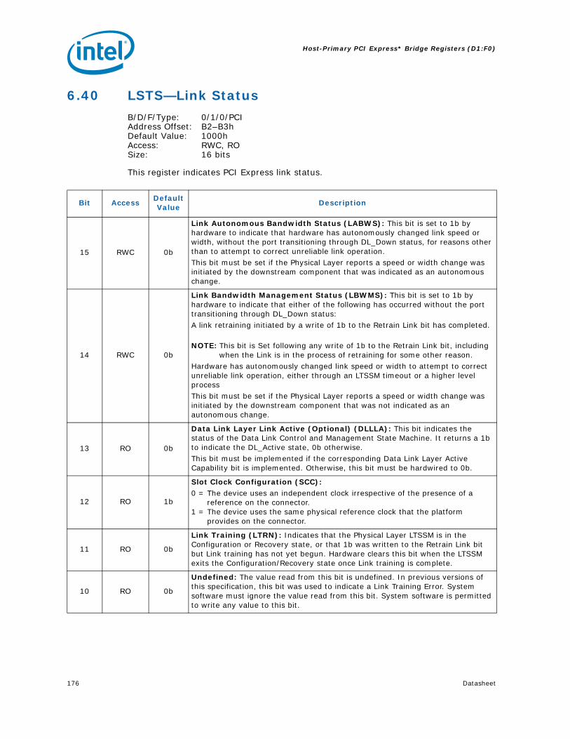
Host-Primary PCI Express* Bridge Registers (D1:F0)
176 Datasheet
6.40 LSTS—Link Status
B/D/F/Type: 0/1/0/PCIAddress Offset: B2–B3hDefault Value: 1000hAccess: RWC, RO Size: 16 bits
This register indicates PCI Express link status.
Bit AccessDefault Value
Description
15 RWC 0b
Link Autonomous Bandwidth Status (LABWS): This bit is set to 1b by hardware to indicate that hardware has autonomously changed link speed or width, without the port transitioning through DL_Down status, for reasons other than to attempt to correct unreliable link operation.This bit must be set if the Physical Layer reports a speed or width change was initiated by the downstream component that was indicated as an autonomous change.
14 RWC 0b
Link Bandwidth Management Status (LBWMS): This bit is set to 1b by hardware to indicate that either of the following has occurred without the port transitioning through DL_Down status:A link retraining initiated by a write of 1b to the Retrain Link bit has completed.
NOTE: This bit is Set following any write of 1b to the Retrain Link bit, including when the Link is in the process of retraining for some other reason.
Hardware has autonomously changed link speed or width to attempt to correct unreliable link operation, either through an LTSSM timeout or a higher level processThis bit must be set if the Physical Layer reports a speed or width change was initiated by the downstream component that was not indicated as an autonomous change.
13 RO 0b
Data Link Layer Link Active (Optional) (DLLLA): This bit indicates the status of the Data Link Control and Management State Machine. It returns a 1b to indicate the DL_Active state, 0b otherwise.This bit must be implemented if the corresponding Data Link Layer Active Capability bit is implemented. Otherwise, this bit must be hardwired to 0b.
12 RO 1b
Slot Clock Configuration (SCC): 0 = The device uses an independent clock irrespective of the presence of a
reference on the connector.1 = The device uses the same physical reference clock that the platform
provides on the connector.
11 RO 0b
Link Training (LTRN): Indicates that the Physical Layer LTSSM is in the Configuration or Recovery state, or that 1b was written to the Retrain Link bit but Link training has not yet begun. Hardware clears this bit when the LTSSM exits the Configuration/Recovery state once Link training is complete.
10 RO 0b
Undefined: The value read from this bit is undefined. In previous versions of this specification, this bit was used to indicate a Link Training Error. System software must ignore the value read from this bit. System software is permitted to write any value to this bit.

Datasheet 177
Host-Primary PCI Express* Bridge Registers (D1:F0)
6.41 SLOTCAP—Slot Capabilities
B/D/F/Type: 0/1/0/PCIAddress Offset: B4–B7hDefault Value: 00040000hAccess: RWO, RO Size: 32 bits
PCI Express Slot related registers.
9:4 RO 00h
Negotiated Link Width (NLW): Indicates negotiated link width. This field is valid only when the link is in the L0, L0s, or L1 states (after link width negotiation is successfully completed).01h = x104h = ‘x4 — This is not a supported PCIe Gen2.0 link width. Link width x4 is only
valid when PCIe Gen1.1 I/O card is used in the secondary port.08h = x8 — This is not a supported PCIe Gen2.0 link width. Link width x8 is only
valid when PCIe Gen1.1 I/O card is used in the secondary port.10h = x16All other encodings are reserved.
3:0 RO 0h
Current Link Speed (CLS): This field indicates the negotiated Link speed of the given PCI Express Link.0001b = 2.5 GT/s PCI Express Link0010b = 5 GT/s PCI Express LinkAll other encodings are reserved. The value in this field is undefined when the Link is not up.
Bit AccessDefault Value
Description
Bit AccessDefault Value
Description
31:19 RWO 0000hPhysical Slot Number (PSN): Indicates the physical slot number attached to this Port.
18 RO 1b Reserved
17 RO 0bElectromechanical Interlock Present (EIP): When set to 1b, this bit indicates that an Electromechanical Interlock is implemented on the chassis for this slot.
16:15 RWO 00b
Slot Power Limit Scale (SPLS): Specifies the scale used for the Slot Power Limit Value.00 = 1.0x01 = 0.1x10 = 0.01x11 = 0.001xIf this field is written, the link sends a Set_Slot_Power_Limit message.
14:7 RWO 00h
Slot Power Limit Value (SPLV): In combination with the Slot Power Limit Scale value, specifies the upper limit on power supplied by slot. Power limit (in Watts) is calculated by multiplying the value in this field by the value in the Slot Power Limit Scale field.If this field is written, the link sends a Set_Slot_Power_Limit message.
6:5 RO 00b Reserved

Host-Primary PCI Express* Bridge Registers (D1:F0)
178 Datasheet
6.42 SLOTCTL—Slot Control
B/D/F/Type: 0/1/0/PCIAddress Offset: B8–B9hDefault Value: 0000hAccess: RO, RW Size: 16 bits
PCI Express Slot related registers.
4 RO 0bPower Indicator Present (PIP): When set to 1b, this bit indicates that a Power Indicator is electrically controlled by the chassis for this slot.
3 RO 0bAttention Indicator Present (AIP): When set to 1b, this bit indicates that an Attention Indicator is electrically controlled by the chassis.
2 RO 0bMRL Sensor Present (MSP): When set to 1b, this bit indicates that an MRL Sensor is implemented on the chassis for this slot.
1 RO 0bPower Controller Present (PCP): When set to 1b, this bit indicates that a software programmable Power Controller is implemented for this slot/adapter (depending on form factor).
0 RO 0bAttention Button Present (ABP): When set to 1b, this bit indicates that an Attention Button for this slot is electrically controlled by the chassis.
Bit AccessDefault Value
Description
Bit AccessDefault Value
Description
15:13 RO 000b Reserved
12 RO 0b
Data Link Layer State Changed Enable (DLLSCE): If the Data Link Layer Link Active capability is implemented, when set to 1b, this field enables software notification when Data Link Layer Link Active field is changed.If the Data Link Layer Link Active capability is not implemented, this bit is permitted to be read-only with a value of 0b.
11 RO 0b
Electromechanical Interlock Control (EIC): If an Electromechanical Interlock is implemented, a write of 1b to this field causes the state of the interlock to toggle. A write of 0b to this field has no effect. A read to this register always returns a 0.
10 RO 0b
Power Controller Control (PCC): If a Power Controller is implemented, this field when written sets the power state of the slot per the defined encodings. Reads of this field must reflect the value from the latest write, unless software issues a write without waiting for the previous command to complete in which case the read value is undefined.Depending on the form factor, the power is turned on/off either to the slot or within the adapter. Note that in some cases the power controller may autonomously remove slot power or not respond to a power-up request based on a detected fault condition, independent of the Power Controller Control setting.The defined encodings are:0 = Power On1 = Power OffIf the Power Controller Implemented field in the Slot Capabilities register is set to 0b, then writes to this field have no effect and the read value of this field is undefined.

Datasheet 179
Host-Primary PCI Express* Bridge Registers (D1:F0)
9:8 RO 00b
Power Indicator Control (PIC): If a Power Indicator is implemented, writes to this field set the Power Indicator to the written state. Reads of this field must reflect the value from the latest write, unless software issues a write without waiting for the previous command to complete in which case the read value is undefined.00 = Reserved 01 = On 10 = Blink 11 = OffIf the Power Indicator Present bit in the Slot Capabilities register is 0b, this field is permitted to be read-only with a value of 00b.
7:6 RO 00b
Attention Indicator Control (AIC): If an Attention Indicator is implemented, writes to this field set the Attention Indicator to the written state.Reads of this field must reflect the value from the latest write, unless software issues a write without waiting for the previous command to complete in which case the read value is undefined. If the indicator is electrically controlled by chassis, the indicator is controlled directly by the downstream port through implementation specific mechanisms.00 = Reserved 01 = On 10 = Blink 11 = OffIf the Attention Indicator Present bit in the Slot Capabilities register is 0b, this field is permitted to be read only with a value of 00b.
5:4 RO 00b Reserved
3 RW 0bPresence Detect Changed Enable (PDCE): When set to 1b, this bit enables software notification on a presence detect changed event.
2 RO 0b
MRL Sensor Changed Enable (MSCE): When set to 1b, this bit enables software notification on a MRL sensor changed event.Default value of this field is 0b. If the MRL Sensor Present field in the Slot Capabilities register is set to 0b, this bit is permitted to be read-only with a value of 0b.
1 RO 0b
Power Fault Detected Enable (PFDE): When set to 1b, this bit enables software notification on a power fault event.Default value of this field is 0b. If Power Fault detection is not supported, this bit is permitted to be read-only with a value of 0b
0 RO 0bButton Pressed Enable (ABPE): When set to 1b, this bit enables software notification on an attention button pressed event.
Bit AccessDefault Value
Description
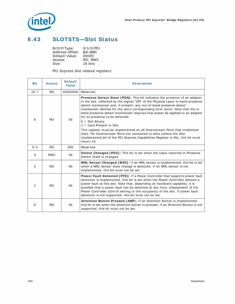
Host-Primary PCI Express* Bridge Registers (D1:F0)
180 Datasheet
6.43 SLOTSTS—Slot Status
B/D/F/Type: 0/1/0/PCIAddress Offset: BA–BBhDefault Value: 0000hAccess: RO, RWC Size: 16 bits
PCI Express Slot related registers.
Bit AccessDefault Value
Description
15:7 RO 0000000b Reserved
6 RO 0b
Presence Detect State (PDS): This bit indicates the presence of an adapter in the slot, reflected by the logical "OR" of the Physical Layer in-band presence detect mechanism and, if present, any out-of-band presence detect mechanism defined for the slot's corresponding form factor. Note that the in-band presence detect mechanism requires that power be applied to an adapter for its presence to be detected. 0 = Slot Empty1 = Card Present in SlotThis register must be implemented on all Downstream Ports that implement slots. For Downstream Ports not connected to slots (where the Slot Implemented bit of the PCI Express Capabilities Register is 0b), this bit must return 1b.
5:4 RO 00b Reserved
3 RWC 0bDetect Changed (PDC): This bit is set when the value reported in Presence Detect State is changed.
2 RO 0bMRL Sensor Changed (MSC): If an MRL sensor is implemented, this bit is set when a MRL Sensor state change is detected. If an MRL sensor is not implemented, this bit must not be set.
1 RO 0b
Power Fault Detected (PFD): If a Power Controller that supports power fault detection is implemented, this bit is set when the Power Controller detects a power fault at this slot. Note that, depending on hardware capability, it is possible that a power fault can be detected at any time, independent of the Power Controller Control setting or the occupancy of the slot. If power fault detection is not supported, this bit must not be set.
0 RO 0bAttention Button Pressed (ABP): If an Attention Button is implemented, this bit is set when the attention button is pressed. If an Attention Button is not supported, this bit must not be set.

Datasheet 181
Host-Primary PCI Express* Bridge Registers (D1:F0)
6.44 RCTL—Root Control
B/D/F/Type: 0/1/0/PCIAddress Offset: BC–BDhDefault Value: 0000hAccess: RO, RW Size: 16 bits
This register allows control of PCI Express Root Complex specific parameters. The system error control bits in this register determine if corresponding SERRs are generated when our device detects an error (reported in this device's Device Status register) or when an error message is received across the link. Reporting of SERR as controlled by these bits takes precedence over the SERR Enable in the PCI Command Register.
Bit AccessDefault Value
Description
15:4 RO 000h Reserved
3 RW 0b
PME Interrupt Enable (PMEIE): 0 = No interrupts are generated as a result of receiving PME messages.1 = Enables interrupt generation upon receipt of a PME message as reflected in
the PME Status bit of the Root Status Register. A PME interrupt is also generated if the PME Status bit of the Root Status Register is set when this bit is set from a cleared state.
2 RW 0b
System Error on Fatal Error Enable (SEFEE): Controls the Root Complex's response to fatal errors.0 = No SERR generated on receipt of fatal error.1 = Indicates that an SERR should be generated if a fatal error is reported by
any of the devices in the hierarchy associated with this Root Port, or by the Root Port itself.
1 RW 0b
System Error on Non-Fatal Uncorrectable Error Enable (SENFUEE): Controls the Root Complex's response to non-fatal errors.0 = No SERR generated on receipt of non-fatal error.1 = Indicates that an SERR should be generated if a non-fatal error is reported
by any of the devices in the hierarchy associated with this Root Port, or by the Root Port itself.
0 RW 0b
System Error on Correctable Error Enable (SECEE): Controls the Root Complex's response to correctable errors.0 = No SERR generated on receipt of correctable error.1 = Indicates that an SERR should be generated if a correctable error is reported
by any of the devices in the hierarchy associated with this Root Port, or by the Root Port itself.

Host-Primary PCI Express* Bridge Registers (D1:F0)
182 Datasheet
6.45 RSTS—Root Status
B/D/F/Type: 0/1/0/PCIAddress Offset: C0–C3hDefault Value: 00000000hAccess: RO, RWC Size: 32 bits
This register provides information about PCI Express Root Complex specific parameters.
6.46 PELC—PCI Express Legacy Control
B/D/F/Type: 0/1/0/PCIAddress Offset: EC–EFhDefault Value: 00000000hAccess: RO, RW Size: 32 bits
This register controls functionality that is needed by Legacy (non-PCI Express aware) OSs during run time.
Bit AccessDefault Value
Description
31:18 RO 0000h Reserved
17 RO 0b
PME Pending (PMEP): Indicates that another PME is pending when the PME Status bit is set. When the PME Status bit is cleared by software; the PME is delivered by hardware by setting the PME Status bit again and updating the Requestor ID appropriately. The PME pending bit is cleared by hardware if no more PMEs are pending.
16 RWC 0bPME Status (PMES): Indicates that PME was asserted by the requestor ID indicated in the PME Requestor ID field. Subsequent PMEs are kept pending until the status register is cleared by writing a 1 to this field.
15:0 RO 0000hPME Requestor ID (PMERID): Indicates the PCI requestor ID of the last PME requestor.
Bit AccessDefault Value
Description
31:3 RO0000000
0hReserved
2 RW 0b
PME GPE Enable (PMEGPE): 0 = Do not generate GPE PME message when PME is received.1 = Generate a GPE PME message when PME is received (Assert_PMEGPE and
Deassert_PMEGPE messages on DMI). This enables the MCH to support PMEs on the PCI Express port under legacy OSs.
1 RO 0b Reserved
0 RW 0b
General Message GPE Enable (GENGPE): 0 = Do not forward received GPE assert/de-assert messages.1 = Forward received GPE assert/de-assert messages. These general GPE
message can be received via the PCI Express port from an external Intel device and will be subsequently forwarded to the ICH (via Assert_GPE and Deassert_GPE messages on DMI).

Datasheet 183
Host-Primary PCI Express* Bridge Registers (D1:F0)
6.47 VCECH—Virtual Channel Enhanced Capability Header
B/D/F/Type: 0/1/0/MMRAddress Offset: 100–103hDefault Value: 14010002hAccess: RO Size: 32 bits
This register indicates PCI Express device Virtual Channel capabilities. Extended capability structures for PCI Express devices are located in PCI Express extended configuration space and have different field definitions than standard PCI capability structures.
6.48 PVCCAP1—Port VC Capability Register 1
B/D/F/Type: 0/1/0/MMRAddress Offset: 104–107hDefault Value: 00000000hAccess: RO Size: 32 bits
This register describes the configuration of PCI Express Virtual Channels associated with this port.
Bit AccessDefault Value
Description
31:20 RO 140hPointer to Next Capability (PNC): The Link Declaration Capability is the next in the PCI Express extended capabilities list.
19:16 RO 1hPCI Express Virtual Channel Capability Version (PCIEVCCV): Hardwired to 1 to indicate compliances with the 1.1 version of the PCI Express specification.Note: This version does not change for 2.0 compliance.
15:0 RO 0002hExtended Capability ID (ECID): Value of 0002 h identifies this linked list item (capability structure) as being for PCI Express Virtual Channel registers.
Bit AccessDefault Value
Description
31:7 RO 00000h Reserved
6:4 RO 000b
Low Priority Extended VC Count (LPEVCC): Indicates the number of (extended) Virtual Channels in addition to the default VC belonging to the low-priority VC (LPVC) group that has the lowest priority with respect to other VC resources in a strict-priority VC Arbitration.The value of 0 in this field implies strict VC arbitration.
3 RO 0b Reserved
2:0 RO 000bExtended VC Count (EVCC): Indicates the number of (extended) Virtual Channels in addition to the default VC supported by the device.

Host-Primary PCI Express* Bridge Registers (D1:F0)
184 Datasheet
6.49 PVCCAP2—Port VC Capability Register 2
B/D/F/Type: 0/1/0/MMRAddress Offset: 108–10BhDefault Value: 00000000hAccess: RO Size: 32 bits
This register describes the configuration of PCI Express Virtual Channels associated with this port.
6.50 PVCCTL—Port VC Control
B/D/F/Type: 0/1/0/MMRAddress Offset: 10C–10DhDefault Value: 0000hAccess: RO, RW Size: 16 bits
Bit AccessDefault Value
Description
31:24 RO 00h
VC Arbitration Table Offset (VCATO): Indicates the location of the VC Arbitration Table. This field contains the zero-based offset of the table in DQWORDS (16 bytes) from the base address of the Virtual Channel Capability Structure. A value of 0 indicates that the table is not present (due to fixed VC priority).
23:0 RO 0000h Reserved
Bit AccessDefault Value
Description
15:4 RO 000h Reserved
3:1 RW 000bVC Arbitration Select (VCAS): This field will be programmed by software to the only possible value as indicated in the VC Arbitration Capability field. Since there is no other VC supported than the default, this field is reserved.
0 RO 0b Reserved

Datasheet 185
Host-Primary PCI Express* Bridge Registers (D1:F0)
6.51 VC0RCAP—VC0 Resource Capability
B/D/F/Type: 0/1/0/MMRAddress Offset: 110–113hDefault Value: 00000001hAccess: RO Size: 32 bits
Bit AccessDefault Value
Description
31:16 RO 0000h Reserved
15 RO 0b
Reject Snoop Transactions (RSNPT): 0 = Transactions with or without the No Snoop bit set within the Transaction
Layer Packet header are allowed on this VC.1 = When Set, any transaction for which the No Snoop attribute is applicable but
is not Set within the TLP Header will be rejected as an Unsupported Request.
14:8 RO 0000h Reserved
7:0 RO 01h
Port Arbitration Capability: Indicates types of Port Arbitration supported by the VC resource. This field is valid for all Switch Ports, Root Ports that support peer-to-peer traffic, and RCRBs, but not for PCI Express Endpoint devices or Root Ports that do not support peer to peer traffic.Each bit location within this field corresponds to a Port Arbitration Capability defined below. When more than one bit in this field is Set, it indicates that the VC resource can be configured to provide different arbitration services.Software selects among these capabilities by writing to the Port Arbitration Select field (see below).Defined bit positions are:Bit[0] = Default = 01b; Non-configurable hardware-fixed arbitration
scheme, e.g., Round Robin (RR)Bit[1] = Weighted Round Robin (WRR) arbitration with 32 phasesBit[2] = WRR arbitration with 64 phasesBit[3] = WRR arbitration with 128 phasesBit[4] = Time-based WRR with 128 phasesBit[5] = WRR arbitration with 256 phasesBits[6:7] = ReservedMCH default indicates "Non-configurable hardware-fixed arbitration scheme".
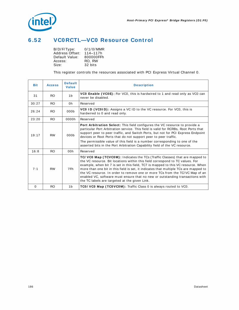
Host-Primary PCI Express* Bridge Registers (D1:F0)
186 Datasheet
6.52 VC0RCTL—VC0 Resource Control
B/D/F/Type: 0/1/0/MMRAddress Offset: 114–117hDefault Value: 800000FFhAccess: RO, RW Size: 32 bits
This register controls the resources associated with PCI Express Virtual Channel 0.
Bit AccessDefault Value
Description
31 RO 1bVC0 Enable (VC0E): For VC0, this is hardwired to 1 and read only as VC0 can never be disabled.
30:27 RO 0h Reserved
26:24 RO 000bVC0 ID (VC0ID): Assigns a VC ID to the VC resource. For VC0, this is hardwired to 0 and read only.
23:20 RO 0000h Reserved
19:17 RW 000b
Port Arbitration Select: This field configures the VC resource to provide a particular Port Arbitration service. This field is valid for RCRBs, Root Ports that support peer to peer traffic, and Switch Ports, but not for PCI Express Endpoint devices or Root Ports that do not support peer to peer traffic.The permissible value of this field is a number corresponding to one of the asserted bits in the Port Arbitration Capability field of the VC resource.
16:8 RO 00h Reserved
7:1 RW 7Fh
TC/VC0 Map (TCVC0M): Indicates the TCs (Traffic Classes) that are mapped to the VC resource. Bit locations within this field correspond to TC values. For example, when bit 7 is set in this field, TC7 is mapped to this VC resource. When more than one bit in this field is set, it indicates that multiple TCs are mapped to the VC resource. In order to remove one or more TCs from the TC/VC Map of an enabled VC, software must ensure that no new or outstanding transactions with the TC labels are targeted at the given Link.
0 RO 1b TC0/VC0 Map (TC0VC0M): Traffic Class 0 is always routed to VC0.

Datasheet 187
Host-Primary PCI Express* Bridge Registers (D1:F0)
6.53 VC0RSTS—VC0 Resource Status
B/D/F/Type: 0/1/0/MMRAddress Offset: 11A–11BhDefault Value: 0002hAccess: ROSize: 16 bits
This register reports the Virtual Channel specific status.
6.54 RCLDECH—Root Complex Link Declaration Enhanced
B/D/F/Type: 0/1/0/MMRAddress Offset: 140–143hDefault Value: 00010005hAccess: RO Size: 32 bits
This capability declares links from this element (PCI Express) to other elements of the root complex component to which it belongs. See PCI Express specification for link/topology declaration requirements.
Bit AccessDefault Value
Description
15:2 RO 0000h Reserved
1 RO 1b
VC0 Negotiation Pending (VC0NP): 0 = The VC negotiation is complete.1 = The VC resource is still in the process of negotiation (initialization or
disabling).This bit indicates the status of the process of Flow Control initialization. It is set by default on Reset, as well as whenever the corresponding Virtual Channel is Disabled or the Link is in the DL_Down state. It is cleared when the link successfully exits the FC_INIT2 state.Before using a Virtual Channel, software must check whether the VC Negotiation Pending fields for that Virtual Channel are cleared in both Components on a Link.
0 RO 0b Reserved
Bit AccessDefault Value
Description
31:20 RO 000hPointer to Next Capability (PNC): This is the last capability in the PCI Express extended capabilities list.
19:16 RO 1hLink Declaration Capability Version (LDCV): Hardwired to 1 to indicate compliances with the 1.1 version of the PCI Express specification.Note: This version does not change for 2.0 compliance.
15:0 RO 0005hExtended Capability ID (ECID): Value of 0005h identifies this linked list item (capability structure) as being for PCI Express Link Declaration Capability.

Host-Primary PCI Express* Bridge Registers (D1:F0)
188 Datasheet
6.55 ESD—Element Self Description
B/D/F/Type: 0/1/0/MMRAddress Offset: 144–147hDefault Value: 02000100hAccess: RO, RWO Size: 32 bits
This register provides information about the root complex element containing this Link Declaration Capability.
6.56 LE1D—Link Entry 1 Description
B/D/F/Type: 0/1/0/MMRAddress Offset: 150–153hDefault Value: 00000000hAccess: RO, RWO Size: 32 bits
This register provides the first part of a Link Entry which declares an internal link to another Root Complex Element.
Bit AccessDefault Value
Description
31:24 RO 02h
Port Number (PN): Specifies the port number associated with this element with respect to the component that contains this element. This port number value is utilized by the egress port of the component to provide arbitration to this Root Complex Element.
23:16 RWO 00hComponent ID (CID): Identifies the physical component that contains this Root Complex Element.
15:8 RO 01hNumber of Link Entries (NLE): Indicates the number of link entries following the Element Self Description. This field reports 1 (to Egress port only as we don't report any peer-to-peer capabilities in our topology).
7:4 RO 0h Reserved
3:0 RO 0h Element Type (ET): Indicates Configuration Space Element.
Bit AccessDefault Value
Description
31:24 RO 00h
Target Port Number (TPN): Specifies the port number associated with the element targeted by this link entry (Egress Port). The target port number is with respect to the component that contains this element as specified by the target component ID.
23:16 RWO 00hTarget Component ID (TCID): Identifies the physical or logical component that is targeted by this link entry.
15:2 RO 0000h Reserved
1 RO 0bLink Type (LTYP): Indicates that the link points to memory-mapped space (for RCRB). The link address specifies the 64-bit base address of the target RCRB.
0 RWO 0bLink Valid (LV): 0 = Link Entry is not valid and will be ignored.1 = Link Entry specifies a valid link.
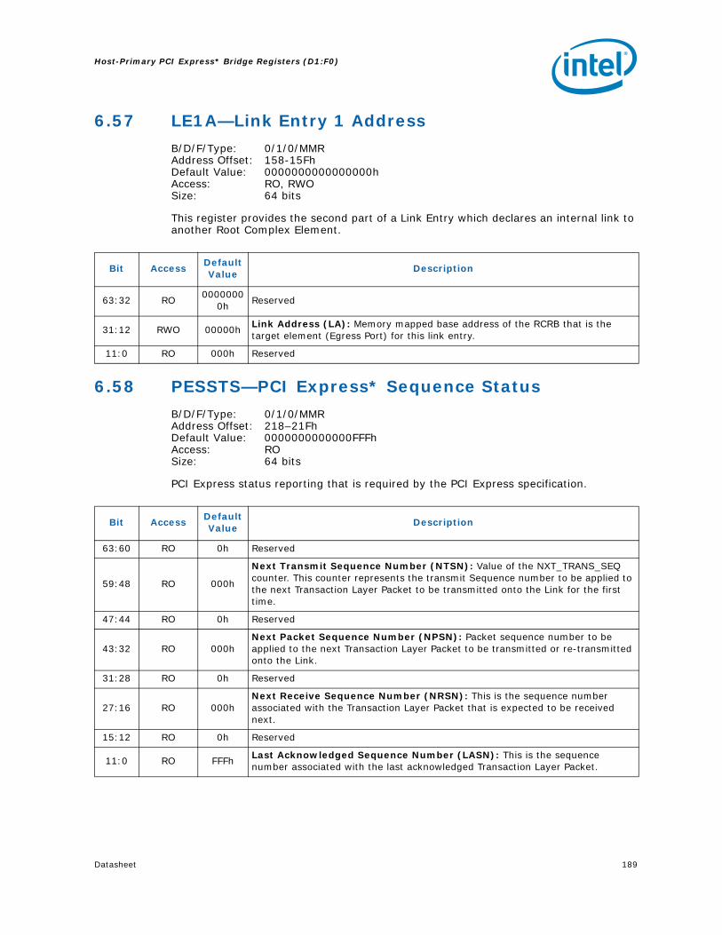
Datasheet 189
Host-Primary PCI Express* Bridge Registers (D1:F0)
6.57 LE1A—Link Entry 1 Address
B/D/F/Type: 0/1/0/MMRAddress Offset: 158-15FhDefault Value: 0000000000000000hAccess: RO, RWO Size: 64 bits
This register provides the second part of a Link Entry which declares an internal link to another Root Complex Element.
6.58 PESSTS—PCI Express* Sequence Status
B/D/F/Type: 0/1/0/MMRAddress Offset: 218–21FhDefault Value: 0000000000000FFFhAccess: RO Size: 64 bits
PCI Express status reporting that is required by the PCI Express specification.
Bit AccessDefault Value
Description
63:32 RO0000000
0hReserved
31:12 RWO 00000hLink Address (LA): Memory mapped base address of the RCRB that is the target element (Egress Port) for this link entry.
11:0 RO 000h Reserved
Bit AccessDefault Value
Description
63:60 RO 0h Reserved
59:48 RO 000h
Next Transmit Sequence Number (NTSN): Value of the NXT_TRANS_SEQ counter. This counter represents the transmit Sequence number to be applied to the next Transaction Layer Packet to be transmitted onto the Link for the first time.
47:44 RO 0h Reserved
43:32 RO 000hNext Packet Sequence Number (NPSN): Packet sequence number to be applied to the next Transaction Layer Packet to be transmitted or re-transmitted onto the Link.
31:28 RO 0h Reserved
27:16 RO 000hNext Receive Sequence Number (NRSN): This is the sequence number associated with the Transaction Layer Packet that is expected to be received next.
15:12 RO 0h Reserved
11:0 RO FFFhLast Acknowledged Sequence Number (LASN): This is the sequence number associated with the last acknowledged Transaction Layer Packet.

Host-Primary PCI Express* Bridge Registers (D1:F0)
190 Datasheet
§ §

Datasheet 191
Intel Manageability Engine Subsystem PCI (D3:F0,F3)
7 Intel Manageability Engine Subsystem PCI (D3:F0,F3)
This chapter provides the register descriptions for Device 3 (D3), Functions 0 (F0) and 3 (F3).
7.1 HECI Function in ME Subsystem (D3:F0)
Device 3 contains registers for the Intel Manageability Engine. The table below lists the PCI configuration registers in order of ascending offset address.
Note: The following sections describe Device 3 configuration registers only.
Table 13. HECI Function in ME Subsystem (D3:F0) Register Address Map
Address Offset
Symbol Register NameDefault Value
Access
0–3h ID Identifiers 29E48086h RO
4–5h CMD Command 0000h RO, RW
6–7h STS Device Status 0010h RO
8h RID Revision IDSee register description
RO
9–Bh CC Class Code 0C8001h RO
Ch CLS Cache Line Size 00h RO
Dh MLT Master Latency Timer 00h RO
Eh HTYPE Header Type 80h RO
10–17h HECI_MBAR HECI MMIO Base Address0000000000
000004hRO, RW
2C–2Fh SS Sub System Identifiers 00000000h RWO
34h CAP Capabilities Pointer 50h RO
3C–3Dh INTR Interrupt Information 0100h RO, RW
3Eh MGNT Minimum Grant 00h RO
3Fh MLAT Maximum Latency 00h RO
40–43h HFS Host Firmware Status 00000000h RO
50–51h PID PCI Power Management Capability ID 8C01h RO
52–53h PC PCI Power Management Capabilities C803h RO
54–55h PMCSPCI Power Management Control And Status
0008hRWC, RO,
RW
8C–8Dh MID Message Signaled Interrupt Identifiers 0005h RO
8E–8Fh MCMessage Signaled Interrupt Message Control
0080h RO, RW
90–93h MAMessage Signaled Interrupt Message Address
00000000h RW, RO
94–97h MUAMessage Signaled Interrupt Upper Address (Optional)
00000000h RW
98–99h MDMessage Signaled Interrupt Message Data
0000h RW
A0h HIDM HECI Interrupt Delivery Mode 00h RW

Intel Manageability Engine Subsystem PCI (D3:F0,F3)
192 Datasheet
7.1.1 ID—Identifiers
B/D/F/Type: 0/3/0/PCIAddress Offset: 0–3hDefault Value: 29E48086hAccess: RO Size: 32 bits
7.1.2 CMD—Command
B/D/F/Type: 0/3/0/PCIAddress Offset: 4–5hDefault Value: 0000hAccess: RO, RW Size: 16 bits
Bit AccessDefault Value
Description
31:16 RO 29E4hDevice ID (DID): Device ID (DID): This field indicates what device number assigned by Intel.
15:0 RO 8086hVendor ID (VID): Vendor ID (VID): This field indicates Intel is the vendor, assigned by the PCI SIG.
Bit AccessDefault Value
Description
15:11 RO 00000b Reserved
10 RW 0bInterrupt Disable (ID): Disables this device from generating PCI line based interrupts. This bit does not have any effect on MSI operation.
9:3 RO 00h Reserved
2 RW 0b
Bus Master Enable (BME): Controls the HECI host controller's ability to act as a system memory master for data transfers. When this bit is cleared, HECI bus master activity stops and any active DMA engines return to an idle condition. This bit is made visible to firmware through the H_PCI_CSR register, and changes to this bit may be configured by the H_PCI_CSR register to generate an ME MSI.0 = HECI is blocked from generating MSI to the host processor.Note that this bit does not block HECI accesses to ME-UMA, i.e. writes or reads to the host and ME circular buffers through the read window and write window registers still cause ME backbone transactions to ME-UMA.
1 RW 0bMemory Space Enable (MSE): Controls access to the HECI host controller’s memory mapped register space.
0 RO 0b Reserved

Datasheet 193
Intel Manageability Engine Subsystem PCI (D3:F0,F3)
7.1.3 STS—Device Status
B/D/F/Type: 0/3/0/PCIAddress Offset: 6–7hDefault Value: 0010hAccess: RO Size: 16 bits
7.1.4 RID—Revision ID
B/D/F/Type: 0/3/0/PCIAddress Offset: 8hDefault Value: see table belowAccess: RO Size: 8 bits
7.1.5 CC—Class Code
B/D/F/Type: 0/3/0/PCIAddress Offset: 9–BhDefault Value: 0C8001hAccess: RO Size: 24 bits
Bit AccessDefault Value
Description
15:5 RO 0h Reserved
4 RO 1bCapabilities List (CL): Indicates the presence of a capabilities list, hardwired to 1.
3 RO 0bInterrupt Status (IS): Indicates the interrupt status of the device 1 = Asserted
2:0 RO 000b Reserved
Bit AccessDefault Value
Description
7:0 ROSee
Description
Revision ID (RID): This field indicates stepping of the HECI host controller. Refer to the Intel® X38 Express Chipset Specification Update for the value of this register.
Bit AccessDefault Value
Description
23:16 RO 0chBase Class Code (BCC): Indicates the base class code of the HECI host controller device.
15:8 RO 80hSub Class Code (SCC): Indicates the sub class code of the HECI host controller device.
7:0 RO 01hProgramming Interface (PI): Indicates the programming interface of the HECI host controller device.

Intel Manageability Engine Subsystem PCI (D3:F0,F3)
194 Datasheet
7.1.6 CLS—Cache Line Size
B/D/F/Type: 0/3/0/PCIAddress Offset: ChDefault Value: 00hAccess: RO Size: 8 bits
7.1.7 MLT—Master Latency Timer
B/D/F/Type: 0/3/0/PCIAddress Offset: DhDefault Value: 00hAccess: RO Size: 8 bits
7.1.8 HTYPE—Header Type
B/D/F/Type: 0/3/0/PCIAddress Offset: EhDefault Value: 80hAccess: RO Size: 8 bits
Bit AccessDefault Value
Description
7:0 RO 00h Cache Line Size (CLS): Not implemented, hardwired to 0.
Bit AccessDefault Value
Description
7:0 RO 00h Master Latency Timer (MLT): Not implemented, hardwired to 0.
Bit AccessDefault Value
Description
7 RO 1bMulti-Function Device (MFD): Indicates the HECI host controller is part of a multi-function device.
6:0 RO 0000000bHeader Layout (HL): Indicates that the HECI host controller uses a target device layout.

Datasheet 195
Intel Manageability Engine Subsystem PCI (D3:F0,F3)
7.1.9 HECI_MBAR—HECI MMIO Base Address
B/D/F/Type: 0/3/0/PCIAddress Offset: 10–17hDefault Value: 0000000000000004hAccess: RO, RW Size: 64 bits
7.1.10 SS—Sub System Identifiers
B/D/F/Type: 0/3/0/PCIAddress Offset: 2C–2FhDefault Value: 00000000hAccess: RWO Size: 32 bits
Bit AccessDefault Value
Description
63:4 RW00000000000000
0hBase Address (BA): Base address of register memory space.
3 RO 0b Prefetchable (PF): Indicates that this range is not pre-fetchable
2:1 RO 10bType (TP): Indicates that this range can be mapped anywhere in 64-bit address space.
0 RO 0bResource Type Indicator (RTE): Indicates a request for register memory space.
Bit AccessDefault Value
Description
31:16 RWO 0000hSubsystem ID (SSID): Indicates the sub-system identifier. This field should be programmed by BIOS during boot-up. Once written, this register becomes Read Only. This field can only be cleared by PLTRST#.
15:0 RWO 0000hSubsystem Vendor ID (SSVID): Indicates the sub-system vendor identifier. This field should be programmed by BIOS during boot-up. Once written, this register becomes Read Only. This field can only be cleared by PLTRST#.
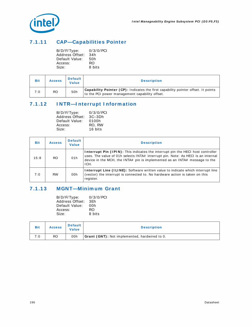
Intel Manageability Engine Subsystem PCI (D3:F0,F3)
196 Datasheet
7.1.11 CAP—Capabilities Pointer
B/D/F/Type: 0/3/0/PCIAddress Offset: 34hDefault Value: 50hAccess: RO Size: 8 bits
7.1.12 INTR—Interrupt Information
B/D/F/Type: 0/3/0/PCIAddress Offset: 3C–3DhDefault Value: 0100hAccess: RO, RW Size: 16 bits
7.1.13 MGNT—Minimum Grant
B/D/F/Type: 0/3/0/PCIAddress Offset: 3EhDefault Value: 00hAccess: RO Size: 8 bits
Bit AccessDefault Value
Description
7:0 RO 50hCapability Pointer (CP): Indicates the first capability pointer offset. It points to the PCI power management capability offset.
Bit AccessDefault Value
Description
15:8 RO 01h
Interrupt Pin (IPIN): This indicates the interrupt pin the HECI host controller uses. The value of 01h selects INTA# interrupt pin. Note: As HECI is an internal device in the MCH, the INTA# pin is implemented as an INTA# message to the ICH.
7:0 RW 00hInterrupt Line (ILINE): Software written value to indicate which interrupt line (vector) the interrupt is connected to. No hardware action is taken on this register.
Bit AccessDefault Value
Description
7:0 RO 00h Grant (GNT): Not implemented, hardwired to 0.

Datasheet 197
Intel Manageability Engine Subsystem PCI (D3:F0,F3)
7.1.14 MLAT—Maximum Latency
B/D/F/Type: 0/3/0/PCIAddress Offset: 3FhDefault Value: 00hAccess: RO Size: 8 bits
7.1.15 HFS—Host Firmware Status
B/D/F/Type: 0/3/0/PCIAddress Offset: 40–43hDefault Value: 00000000hAccess: RO Size: 32 bits
7.1.16 PID—PCI Power Management Capability ID
B/D/F/Type: 0/3/0/PCIAddress Offset: 50–51hDefault Value: 8C01hAccess: RO Size: 16 bits
Bit AccessDefault Value
Description
7:0 RO 00h Latency (LAT): Not implemented, hardwired to 0.
Bit AccessDefault Value
Description
31:0 RO0000000
0h
Firmware Status Host Access (FS_HA): Indicates current status of the firmware for the HECI controller. This field is the host's read only access to the FS field in the ME Firmware Status AUX register.
Bit AccessDefault Value
Description
15:8 RO 8ChNext Capability (NEXT): Indicates the location of the next capability item in the list. This is the Message Signaled Interrupts capability.
7:0 RO 01h Cap ID (CID): Indicates that this pointer is a PCI power management.

Intel Manageability Engine Subsystem PCI (D3:F0,F3)
198 Datasheet
7.1.17 PC—PCI Power Management Capabilities
B/D/F/Type: 0/3/0/PCIAddress Offset: 52–53hDefault Value: C803hAccess: RO Size: 16 bits
7.1.18 PMCS—PCI Power Management Control And Status
B/D/F/Type: 0/3/0/PCIAddress Offset: 54–55hDefault Value: 0008hAccess: RWC, RO, RW Size: 16 bits
Bit AccessDefault Value
Description
15:11 RO 11001bPME_Support (PSUP): Indicates the states that can generate PME#. HECI can assert PME# from any D-state except D1 or D2 which are not supported by HECI.
10 RO 0b D2_Support (D2S): The D2 state is not supported for the HECI host controller.
9 RO 0b D1_Support (D1S): The D1 state is not supported for the HECI host controller.
8:6 RO 000bAux_Current (AUXC): Reports the maximum Suspend well current required when in the D3COLD state.
5 RO 0bDevice Specific Initialization (DSI): Indicates whether device-specific initialization is required.
4 RO 0b Reserved
3 RO 0b PME Clock (PMEC): Indicates that PCI clock is not required to generate PME#.
2:0 RO 011bVersion (VS): Indicates support for Revision 1.2 of the PCI Power Management Specification.
Bit AccessDefault Value
Description
15 RWC 0b
PME Status (PMES): The PME Status bit in HECI space can be set to '1' by ME FW performing a write into AUX register to set PMES.This bit is cleared by host processor writing a '1' to it.ME cannot clear this bit.Host processor writes with value '0' have no effect on this bit.This bit is reset to '0' by MRST#
14:9 RO 000000b Reserved
8 RW 0b
PME Enable (PMEE): This bit is read/write, under control of host SW. It does not directly have an effect on PME events. However, this bit is shadowed into AUX space so ME FW can monitor it. The ME FW is responsible for ensuring that FW does not cause the PME-S bit to transition to '1' while the PMEE bit is '0', indicating that host SW had disabled PME.This bit is reset to '0' by MRST#
7:4 RO 0000b Reserved

Datasheet 199
Intel Manageability Engine Subsystem PCI (D3:F0,F3)
7.1.19 MID—Message Signaled Interrupt Identifiers
B/D/F/Type: 0/3/0/PCIAddress Offset: 8C–8DhDefault Value: 0005hAccess: RO Size: 16 bits
7.1.20 MC—Message Signaled Interrupt Message Control
B/D/F/Type: 0/3/0/PCIAddress Offset: 8E–8FhDefault Value: 0080hAccess: RO, RW Size: 16 bits
3 RO 1bNo_Soft_Reset (NSR): This bit indicates that when the HECI host controller is transitioning from D3hot to D0 due to power state command, it does not perform an internal reset.
2 RO 0b Reserved
1:0 RW 00b
Power State (PS): This field is used both to determine the current power state of the HECI host controller and to set a new power state. The values are: 00 = D0 state 11 = D3HOT state The D1 and D2 states are not supported for this HECI host controller. When in the D3HOT state, the HBA’s configuration space is available, but the register memory spaces are not. Additionally, interrupts are blocked.
Bit AccessDefault Value
Description
Bit AccessDefault Value
Description
15:8 RO 00hNext Pointer (NEXT): Indicates the next item in the list. This can be other capability pointers (such as PCI-X or PCI-Express) or it can be the last item in the list.
7:0 RO 05h Capability ID (CID): Capabilities ID indicates MSI.
Bit AccessDefault Value
Description
15:8 RO 00h Reserved
7 RO 1b64 Bit Address Capable (C64): Specifies whether capable of generating 64-bit messages.
6:4 RO 000b Multiple Message Enable (MME): Not implemented, hardwired to 0.
3:1 RO 000b Multiple Message Capable (MMC): Not implemented, hardwired to 0.
0 RW 0bMSI Enable (MSIE): If set, MSI is enabled and traditional interrupt pins are not used to generate interrupts.

Intel Manageability Engine Subsystem PCI (D3:F0,F3)
200 Datasheet
7.1.21 MA—Message Signaled Interrupt Message Address
B/D/F/Type: 0/3/0/PCIAddress Offset: 90–93hDefault Value: 00000000hAccess: RW, RO Size: 32 bits
7.1.22 MUA—Message Signaled Interrupt Upper Address (Optional)
B/D/F/Type: 0/3/0/PCIAddress Offset: 94–97hDefault Value: 00000000hAccess: RW Size: 32 bits
7.1.23 MD—Message Signaled Interrupt Message Data
B/D/F/Type: 0/3/0/PCIAddress Offset: 98–99hDefault Value: 0000hAccess: RW Size: 16 bits
Bit AccessDefault Value
Description
31:2 RW0000000
0hAddress (ADDR): Lower 32 bits of the system specified message address, always DW aligned.
1:0 RO 00b Reserved
Bit AccessDefault Value
Description
31:0 RW0000000
0hUpper Address (UADDR): Upper 32 bits of the system specified message address. This register is optional and only implemented if MC.C64=1.
Bit AccessDefault Value
Description
15:0 RW 0000hData (Data): This 16-bit field is programmed by system software if MSI is enabled. Its content is driven onto the FSB during the data phase of the MSI memory write transaction.

Datasheet 201
Intel Manageability Engine Subsystem PCI (D3:F0,F3)
7.1.24 HIDM—HECI Interrupt Delivery Mode
B/D/F/Type: 0/3/0/PCIAddress Offset: A0hDefault Value: 00hAccess: RW Size: 8 bitsBIOS Optimal Default 00h
This register is used to select interrupt delivery mechanism for HECI to Host processor interrupts.
Bit AccessDefault Value
Description
7:2 RO 0h Reserved
1:0 RW 00b
HECI Interrupt Delivery Mode (HIDM): These bits control what type of interrupt the HECI will send when ME FW writes to set the M_IG bit in AUX space. They are interpreted as follows:00 = Generate Legacy or MSI interrupt01 = Generate SCI
10 = Generate SMI

Intel Manageability Engine Subsystem PCI (D3:F0,F3)
202 Datasheet
7.2 KT IO/ Memory Mapped Device Specific Registers [D3:F3]
7.2.1 KTRxBR—KT Receive Buffer
B/D/F/Type: 0/3/3/KT MM/IOAddress Offset: 0hDefault Value: 00hAccess: RO/V Size: 8 bits
This implements the KT Receiver Data register. Host access to this address, depends on the state of the DLAB bit {KTLCR[7]). It must be 0 to access the KTRxBR.
RxBR:
Host reads this register when FW provides it the receive data in non-FIFO mode. In FIFO mode, host reads to this register translate into a read from ME memory (RBR FIFO).
Note: Reset: Host System Reset or D3->D0 transition.
Table 14. KT IO/Memory Mapped Register Address Map
Address Offset
Register Symbol
Register NameDefault Value
Access
0h KTRxBR KT Receive Buffer 00h RO/V
0h KTTHR KT Transmit Holding 00h WO
0h KTDLLR KT Divisor Latch LSB 00h RW/V
1h KTIER KT Interrupt Enable 00h RW/V, RO/V
1h KTDLMR KT Divisor Latch MSB 00h RW/V
2h KTIIR KT Interrupt Identification 01h RO
2h KTFCR KT FIFO Control 00h WO
3h KTLCR KT Line Control 03h RW
4h KTMCR KT Modem Control 00h RO, RW
5h KTLSR KT Line Status 00h RO, RO/CR
6h KTMSR KT Modem Status 00h RO, RO/CR
7h KTSCR KT Scratch 00h RW
Bit AccessDefault Value
Description
7:0 RO/V 00hReceiver Buffer Register (RBR): Implements the Data register of the Serial Interface. If the Host does a read, it reads from the Receive Data Buffer.

Datasheet 203
Intel Manageability Engine Subsystem PCI (D3:F0,F3)
7.2.2 KTTHR—KT Transmit Holding
B/D/F/Type: 0/3/3/KT MM/IOAddress Offset: 0hDefault Value: 00hAccess: WO Size: 8 bits
This implements the KT Transmit Data register. Host access to this address, depends on the state of the DLAB bit {KTLCR[7]). It must be 0 to access the KTTHR.
THR:
When host wants to transmit data in the non-FIFO mode, it writes to this register. In FIFO mode, writes by host to this address cause the data byte to be written by hardware to ME memory (THR FIFO).
Note: Reset: Host System Reset or D3->D0 transition.
7.2.3 KTDLLR—KT Divisor Latch LSB
B/D/F/Type: 0/3/3/KT MM/IOAddress Offset: 0hDefault Value: 00hAccess: RW/V Size: 8 bits
This register implements the KT DLL register. Host can Read/Write to this register only when the DLAB bit (KTLCR[7]) is 1. When this bit is 0, Host accesses the KTTHR or the KTRBR depending on Read or Write.
This is the standard Serial Port Divisor Latch register. This register is only for software compatibility and does not affect performance of the hardware.
Note: Reset: Host System Reset or D3->D0 transition.
Bit AccessDefault Value
Description
7:0 WO 00hTransmit Holding Register (THR): Implements the Transmit Data register of the Serial Interface. If Host does a write, it writes to the Transmit Holding Register.
Bit AccessDefault Value
Description
7:0 RW/V 00h Divisor Latch LSB (DLL): Implements the DLL register of the Serial Interface.

Intel Manageability Engine Subsystem PCI (D3:F0,F3)
204 Datasheet
7.2.4 KTIER—KT Interrupt Enable
B/D/F/Type: 0/3/3/KT MM/IOAddress Offset: 1hDefault Value: 00hAccess: RW/V, RO/V Size: 8 bits
This implements the KT Interrupt Enable register. Host access to this address, depends on the state of the DLAB bit {KTLCR[7]). It must be "0" to access this register. The bits enable specific events to interrupt the Host. See bit specific definition.
Note: Reset: Host System Reset or D3 -> D0 transition.
7.2.5 KTDLMR—KT Divisor Latch MSB
B/D/F/Type: 0/3/3/KT MM/IOAddress Offset: 1hDefault Value: 00hAccess: RW/V Size: 8 bits
Host can Read/Write to this register only when the DLAB bit (KTLCR[7]) is 1. When this bit is 0, Host accesses the KTIER.
This is the standard Serial interface's Divisor Latch register's MSB. This register is only for software compatibility and does not affect performance of the hardware.
Note: Reset: Host System Reset or D3->D0 transition.
Bit AccessDefault Value
Description
7:4 RO/V 0h Reserved
3 RW/V 0bMSR (IER2): When set, this bit enables bits in Modem Status register to cause an interrupt to host
2 RW/V 0bLSR (IER1): When set, this bit enables bits in Receiver Line Status Register to cause an Interrupt to Host
1 RW/V 0bTHR (IER1): When set, this bit enables interrupt to be sent to Host when the tranmit Holding register is empty
0 RW/V 0bDR (IER0): When set, Received Data Ready (or Receive FIFO Timeout) interrupts are enabled to be sent to Host.
Bit AccessDefault Value
Description
7:0 RW/V 00hDivisor Latch MSB (DLM): Implements the Divisor Latch MSB register of the Serial Interface.

Datasheet 205
Intel Manageability Engine Subsystem PCI (D3:F0,F3)
7.2.6 KTIIR—KT Interrupt Identification
B/D/F/Type: 0/3/3/KT MM/IOAddress Offset: 2hDefault Value: 01hAccess: RO Size: 8 bits
The KT IIR register prioritizes the interrupts from the function into 4 levels and records them in the IIR_STAT field of the register. When Host accesses the IIR, hardware freezes all interrupts and provides the priority to the Host. Hardware continues to monitor the interrupts but does not change its current indication until the Host read is over. Table in the Host Interrupt Generation section shows the contents.
Note: Reset: See specific Bit descriptions
Bit AccessDefault Value
Description
7 RO 0bFIFO Enable (FIEN1): This bit is connected by hardware to bit 0 in the FCR register. Reset: Host System Reset or D3->D0 transition
6 RO 0bFIFO Enable (FIEN0): This bit is connected by hardware to bit 0 in the FCR register.Reset: Host System Reset or D3->D0 transition
5:4 RO 00b Reserved
3:1 RO 000b
IIR STATUS (IIRSTS): These bits are asserted by the hardware according to the source of the interrupt and the priority level. Refer to the section on Host Interrupt Generation for a table of values.Reset: ME system Reset
0 RO 1bInterrupt Status (INTSTS): When "0" indicates pending interrupt to HostWhen "1" indicates no pending interrupt to Host. Reset: Host system Reset or D3->D0 transition

Intel Manageability Engine Subsystem PCI (D3:F0,F3)
206 Datasheet
7.2.7 KTFCR—KT FIFO Control
B/D/F/Type: 0/3/3/KT MM/IOAddress Offset: 2hDefault Value: 00hAccess: WO Size: 8 bits
When Host writes to this address, it writes to the KTFCR. The FIFO control Register of the serial interface is used to enable the FIFO's, set the receiver FIFO trigger level and clear FIFO's under the direction of the Host.
When Host reads from this address, it reads the KTIIR.
Note: Reset: Host System Reset or D3->D0 transition.
Bit AccessDefault Value
Description
7:6 WO 00b
Receiver Trigger Level (RTL): Trigger level in bytes for the RCV FIFO. Once the trigger level number of bytes is reached, an interrupt is sent to the Host.
00 = 01 01 = 0410 = 0811 = 14
5:4 WO 00b Reserved
3 WO 0b RDY Mode (RDYM): This bit has no affect on hardware performance.
2 WO 0bXMT FIFO Clear (XFIC): When the Host writes one to this bit, the hardware will clear the XMT FIFO. This bit is self-cleared by hardware.
1 WO 0bRCV FIFO Clear (RFIC): When the Host writes one to this bit the hardware will clear the RCV FIFO. This bit is self-cleared by hardware.
0 WO 0bFIFO Enable (FIE): When set, this bit indicates that the KT interface is working in FIFO node. When this bit value is changed, the RCV and XMT FIFO are cleared by hardware.
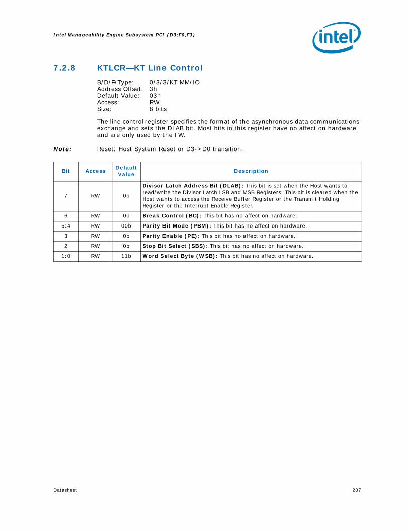
Datasheet 207
Intel Manageability Engine Subsystem PCI (D3:F0,F3)
7.2.8 KTLCR—KT Line Control
B/D/F/Type: 0/3/3/KT MM/IOAddress Offset: 3hDefault Value: 03hAccess: RW Size: 8 bits
The line control register specifies the format of the asynchronous data communications exchange and sets the DLAB bit. Most bits in this register have no affect on hardware and are only used by the FW.
Note: Reset: Host System Reset or D3->D0 transition.
Bit AccessDefault Value
Description
7 RW 0b
Divisor Latch Address Bit (DLAB): This bit is set when the Host wants to read/write the Divisor Latch LSB and MSB Registers. This bit is cleared when the Host wants to access the Receive Buffer Register or the Transmit Holding Register or the Interrupt Enable Register.
6 RW 0b Break Control (BC): This bit has no affect on hardware.
5:4 RW 00b Parity Bit Mode (PBM): This bit has no affect on hardware.
3 RW 0b Parity Enable (PE): This bit has no affect on hardware.
2 RW 0b Stop Bit Select (SBS): This bit has no affect on hardware.
1:0 RW 11b Word Select Byte (WSB): This bit has no affect on hardware.

Intel Manageability Engine Subsystem PCI (D3:F0,F3)
208 Datasheet
7.2.9 KTMCR—KT Modem Control
B/D/F/Type: 0/3/3/KT MM/IOAddress Offset: 4hDefault Value: 00hAccess: RO, RW Size: 8 bits
The Modem Control Register controls the interface with the modem. Since the FW emulates the modem, the Host communicates to the FW via this register. Register has impact on hardware when the Loopback mode is on.
Note: Reset: Host system Reset or D3->D0 transition.
Bit AccessDefault Value
Description
7:5 RO 000b Reserved
4 RW 0bLoop Back Mode (LBM): When set by Host, this bit indicates that the serial port is in loop Back mode. This means that the data that is transmitted by the host should be received. Helps in debug of the interface.
3 RW 0bOutput 2 (OUT2): This bit has no affect on hardware in normal mode. In loop back mode the value of this bit is written by hardware to Modem Status Register bit 7.
2 RW 0bOutput 1 (OUT1): This bit has no affect on hardware in normal mode. In loop back mode the value of this bit is written by hardware to Modem Status Register bit 6.
1 RW 0bRequest to Send Out (RTSO): This bit has no affect on hardware in normal mode. In loopback mode, the value of this bit is written by hardware to Modem Status Register bit 4.
0 RW 0bData Terminal Ready Out (DRTO): This bit has no affect on hardware in normal mode. In loopback mode, the value in this bit is written by hardware to Modem Status Register Bit 5.

Datasheet 209
Intel Manageability Engine Subsystem PCI (D3:F0,F3)
7.2.10 KTLSR—KT Line Status
B/D/F/Type: 0/3/3/KT MM/IOAddress Offset: 5hDefault Value: 00hAccess: RO, RO/CR Size: 8 bits
This register provides status information of the data transfer to the Host. Error indication, etc., are provided by the hardware(HW)/firmware(FW) to the host via this register.
Note: Reset: Host system reset or D3->D0 transition.
Bit AccessDefault Value
Description
7 RO 0bRX FIFO Error (RXFER): This bit is cleared in non FIFO mode. Bit is connected to the BI bit in FIFO mode.
6 RO 0bTransmit Shift Register Empty (TEMT): This bit is connected by hardware to bit 5 (THRE) of this register
5 RO 0b
Transmit Holding Register Empty (THRE): The bit is always set when the mode (FIFO/Non-FIFO) is changed by the Host. This bit is active only when the THR operation is enabled by the FW. This bit has acts differently in the different modes: • Non FIFO Mode: This bit is cleared by hardware when the Host writes to the THR
registers and set by hardware when the FW reads the THR register.• FIFO Mode: This bit is set by hardware when the THR FIFO is empty, and cleared by
hardware when the THR FIFO is not empty.
This bit is reset on Host system reset or D3->D0 transition.
4 RO/CR 0b
Break Interrupt (BI): This bit is cleared by hardware when the LSR register is being read by the Host.This bit is set by hardware in two cases: • FIFO Mode: The FW sets the BI bit by setting the SBI bit in the KTRIVR register (See
KT AUX registers)• Non FIFO Mode: the FW sets the BI bit by setting the BIA bit in the KTRxBR register
(see KT AUX registers)
3:2 RO 00b Reserved
1 RO/CR 0bOverrun Error (OE): This bit is cleared by hardware when the LSR register is being read by the Host. The FW typically sets this bit, but it is cleared by hardware when the host reads the LSR.
0 RO 0b
Data Ready (DR): • Non-FIFO Mode: This bit is set when the FW writes to the RBR register and cleared by
hardware when the RBR register is being Read by the Host.• FIFO Mode: This bit is set by hardware when the RBR FIFO is not empty and cleared by
hardware when the RBR FIFO is empty.
This bit is reset on Host System Reset or D3->D0 transition

Intel Manageability Engine Subsystem PCI (D3:F0,F3)
210 Datasheet
7.2.11 KTMSR—KT Modem Status
B/D/F/Type: 0/3/3/KT MM/IOAddress Offset: 6hDefault Value: 00hAccess: RO, RO/CR Size: 8 bits
The functionality of the Modem is emulated by the FW. This register provides the status of the current state of the control lines from the modem.
Note: Reset: Host system Reset or D3->D0 transition.
7.2.12 KTSCR—KT Scratch
B/D/F/Type: 0/3/3/KT MM/IOAddress Offset: 7hDefault Value: 00hAccess: RW Size: 8 bits
This register has no affect on hardware. This is for the programmer to hold data temporarily.
Note: Reset: Host system reset or D3->D0 transition
§ §
Bit AccessDefault Value
Description
7 RO 0bData Carrier Detect (DCD): In Loop Back mode this bit is connected by hardware to the value of MCR bit 3
6 RO 0bRing Indicator (RI): In Loop Back mode this bit is connected by hardware to the value of MCR bit 2.
5 RO 0bData Set Ready (DSR): In Loop Back mode this bit is connected by hardware to the value of MCR bit 0.
4 RO 0bClear To Send (CTS): In Loop Back mode this bit is connected by hardware to the value of MCR bit 1.
3 RO/CR 0bDelta Data Carrier Detect (DDCD): This bit is set when bit 7 is changed. This bit is cleared by hardware when the MSR register is being read by the HOST driver.
2 RO/CR 0bTrailing Edge of Read Detector (TERI): This bit is set when bit 6 is changed from 1 to 0. This bit is cleared by hardware when the MSR register is being read by the Host driver.
1 RO/CR 0bDelta Data Set Ready (DDSR): This bit is set when bit 5 is changed. This bit is cleared by hardware when the MSR register is being read by the Host driver.
0 RO/CR 0bDelta Clear To Send (DCTS): This bit is set when bit 4 is changed. This bit is cleared by hardware when the MSR register is being read by the Host driver.
Bit AccessDefault Value
Description
7:0 RW 00h Scratch Register Data (SCRD):

Datasheet 211
Host-Secondary PCI Express* Bridge Registers (D6:F0)
8 Host-Secondary PCI Express* Bridge Registers (D6:F0)
Device 6 contains the controls associated with the PCI Express root port that is the intended attach point for external devices. In addition, it also functions as the virtual PCI-to-PCI bridge. The table below provides an address map of the D1:F0 registers listed by address offset in ascending order. This chapter provides a detailed bit description of the registers.
Warning: When reading the PCI Express "conceptual" registers such as this, you may not get a valid value unless the register value is stable.
The PCI Express* Specification defines two types of reserved bits:
Reserved and Preserved:
• Reserved for future RW implementations; software must preserve value read for writes to bits.
• Reserved and Zero: Reserved for future R/WC/S implementations; software must use 0 for writes to bits.
Unless explicitly documented as Reserved and Zero, all bits marked as reserved are part of the Reserved and Preserved type, which have historically been the typical definition for Reserved.
Note: Most (if not all) control bits in this device cannot be modified unless the link is down. Software is required to first disable the link, then program the registers, and then re-enable the link (which will cause a full-retrain with the new settings).
Table 15. Host-Secondary PCI Express* Bridge Register Address Map (D6:F0) (Sheet 1 of 3)
Address Offset
Register Symbol
Register NameDefault Value
Access
0–1h VID1 Vendor Identification 8086h RO
2–3h DID1 Device Identification 29E9h RO
4–5h PCICMD1 PCI Command 0000h RO, RW
6–7h PCISTS1 PCI Status 0010h RO, RWC
8h RID1 Revision IdentificationSee register description
RO
9–Bh CC1 Class Code 060400h RO
Ch CL1 Cache Line Size 00h RW
Eh HDR1 Header Type 01h RO
18h PBUSN1 Primary Bus Number 00h RO
19h SBUSN1 Secondary Bus Number 00h RW
1Ah SUBUSN1 Subordinate Bus Number 00h RW
1Ch IOBASE1 I/O Base Address F0h RO, RW
1Dh IOLIMIT1 I/O Limit Address 00h RW, RO

Host-Secondary PCI Express* Bridge Registers (D6:F0)
212 Datasheet
1E–1Fh SSTS1 Secondary Status 0000h RO, RWC
20–21h MBASE1 Memory Base Address FFF0h RW, RO
22–23h MLIMIT1 Memory Limit Address 0000h RW, RO
24–25h PMBASE1 Prefetchable Memory Base Address FFF1h RW, RO
26–27h PMLIMIT1 Prefetchable Memory Limit Address 0001h RO, RW
28–2Bh PMBASEU1 Prefetchable Memory Base Address Upper 00000000h RW
2C–2Fh PMLIMITU1 Prefetchable Memory Limit Address Upper 00000000h RW
34h CAPPTR1 Capabilities Pointer 88h RO
3Ch INTRLINE1 Interrupt Line 00h RW
3Dh INTRPIN1 Interrupt Pin 01h RO
3E–3Fh BCTRL1 Bridge Control 0000h RO, RW
80–83h PM_CAPID1 Power Management Capabilities C8039001h RO
84–87h PM_CS1 Power Management Control/Status 00000008hRO, RW, RW/P
88–8Bh SS_CAPID Subsystem ID and Vendor ID Capabilities 0000800Dh RO
8C–8Fh SS Subsystem ID and Subsystem Vendor ID 00008086h RWO
90–91h MSI_CAPID Message Signaled Interrupts Capability ID A005h RO
92–93h MC Message Control 0000h RW, RO
94–97h MA Message Address 00000000h RO, RW
98–99h MD Message Data 0000h RW
A0–A1h PE_CAPL PCI Express Capability List 0010h RO
A2–A3h PE_CAP PCI Express Capabilities 0142h RO, RWO
A4–A7h DCAP Device Capabilities 00008000h RO
A8–A9h DCTL Device Control 0000h RW, RO
AA–ABh DSTS Device Status 0000h RO, RWC
AC–AFh LCAP Link Capabilities 03214D02h RO, RWO
B0–B1h LCTL Link Control 0000hRO, RW, RW/SC
B2–hB3 LSTS Link Status 1000h RWC, RO
B4–B7h SLOTCAP Slot Capabilities 00040000h RWO, RO
B8–B9h SLOTCTL Slot Control 0000h RO, RW
BA–BBh SLOTSTS Slot Status 0000h RO, RWC
BC–BDh RCTL Root Control 0000h RO, RW
C0–C3h RSTS Root Status 00000000h RO, RWC
EC–EFh PELC PCI Express Legacy Control 00000000h RO, RW
100–103h VCECHVirtual Channel Enhanced Capability Header
14010002h RO
Table 15. Host-Secondary PCI Express* Bridge Register Address Map (D6:F0) (Sheet 2 of 3)
Address Offset
Register Symbol
Register NameDefault Value
Access
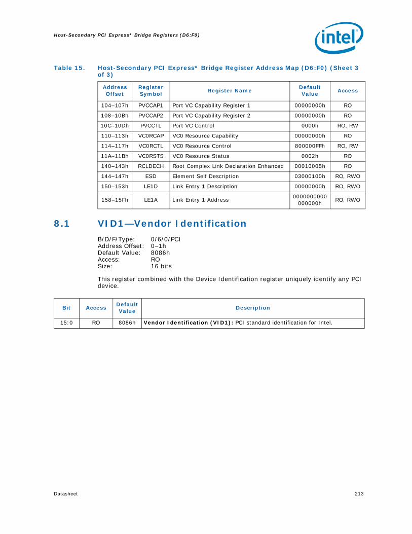
Datasheet 213
Host-Secondary PCI Express* Bridge Registers (D6:F0)
8.1 VID1—Vendor Identification
B/D/F/Type: 0/6/0/PCIAddress Offset: 0–1hDefault Value: 8086hAccess: RO Size: 16 bits
This register combined with the Device Identification register uniquely identify any PCI device.
104–107h PVCCAP1 Port VC Capability Register 1 00000000h RO
108–10Bh PVCCAP2 Port VC Capability Register 2 00000000h RO
10C–10Dh PVCCTL Port VC Control 0000h RO, RW
110–113h VC0RCAP VC0 Resource Capability 00000000h RO
114–117h VC0RCTL VC0 Resource Control 800000FFh RO, RW
11A–11Bh VC0RSTS VC0 Resource Status 0002h RO
140–143h RCLDECH Root Complex Link Declaration Enhanced 00010005h RO
144–147h ESD Element Self Description 03000100h RO, RWO
150–153h LE1D Link Entry 1 Description 00000000h RO, RWO
158–15Fh LE1A Link Entry 1 Address0000000000
000000hRO, RWO
Table 15. Host-Secondary PCI Express* Bridge Register Address Map (D6:F0) (Sheet 3 of 3)
Address Offset
Register Symbol
Register NameDefault Value
Access
Bit AccessDefault Value
Description
15:0 RO 8086h Vendor Identification (VID1): PCI standard identification for Intel.

Host-Secondary PCI Express* Bridge Registers (D6:F0)
214 Datasheet
8.2 DID1—Device Identification
B/D/F/Type: 0/6/0/PCIAddress Offset: 2–3hDefault Value: 29E9hAccess: RO Size: 16 bits
This register combined with the Vendor Identification register uniquely identifies any PCI device.
8.3 PCICMD1—PCI Command
B/D/F/Type: 0/6/0/PCIAddress Offset: 4–5hDefault Value: 0000hAccess: RO, RW Size: 16 bits
Bit AccessDefault Value
Description
15:8 RO 29hDevice Identification Number (DID1(UB)): Identifier assigned to the MCH device #6 (virtual PCI-to-PCI bridge, PCI Express port).
7:4 RO EhDevice Identification Number (DID1(HW)): Identifier assigned to the MCH device #6 (virtual PCI-to-PCI bridge, PCI Express port).
3:0 RO 9hDevice Identification Number (DID1(LB)): Identifier assigned to the MCH device #6 (virtual PCI-to-PCI bridge, PCI Express port).
Bit AccessDefault Value
Description
15:11 RO 00h Reserved
10 RW 0b
INTA Assertion Disable (INTAAD): 0 = This device is permitted to generate INTA interrupt messages.1 = This device is prevented from generating interrupt messages. Any INTA
emulation interrupts already asserted must be de-asserted when this bit is set.
This bit only affects interrupts generated by the device (PCI INTA from a PME event) controlled by this command register. It does not affect upstream MSIs, upstream PCI INTA-INTD assert and de-assert messages.
9 RO 0bFast Back-to-Back Enable (FB2B): Not Applicable or Implemented. Hardwired to 0.

Datasheet 215
Host-Secondary PCI Express* Bridge Registers (D6:F0)
8 RW 0b
SERR# Message Enable (SERRE1): This bit controls Device 6 SERR# messaging. The MCH communicates the SERR# condition by sending a SERR message to the ICH. This bit, when set, enables reporting of non-fatal and fatal errors detected by the device to the Root Complex. Note that errors are reported if enabled either through this bit or through the PCI-Express specific bits in the Device Control Register.0 = The SERR message is generated by the MCH for Device 6 only under
conditions enabled individually through the Device Control Register.1 = The MCH is enabled to generate SERR messages which will be sent to the
ICH for specific Device 6 error conditions generated/detected on the primary side of the virtual PCI to PCI bridge (not those received by the secondary side). The status of SERRs generated is reported in the PCISTS1 register.
7 RO 0b Reserved
6 RW 0b
Parity Error Response Enable (PERRE): Controls whether or not the Master Data Parity Error bit in the PCI Status register can bet set.0 = Master Data Parity Error bit in PCI Status register can NOT be set.1 = Master Data Parity Error bit in PCI Status register CAN be set.
5:3 RO 0b Reserved
2 RW 0b
Bus Master Enable (BME): Controls the ability of the PCI Express port to forward Memory and I/O Read/Write Requests in the upstream direction.0 = This device is prevented from making memory or IO requests to its primary
bus. Note that according to PCI Specification, as MSI interrupt messages are in-band memory writes, disabling the bus master enable bit prevents this device from generating MSI interrupt messages or passing them from its secondary bus to its primary bus. Upstream memory writes/reads, IO writes/reads, peer writes/reads, and MSIs will all be treated as illegal cycles. Writes are forwarded to memory address C0000h with byte enables de-asserted. Reads will be forwarded to memory address C0000h and will return Unsupported Request status (or Master abort) in its completion packet.
1 = This device is allowed to issue requests to its primary bus. Completions for previously issued memory read requests on the primary bus will be issued when the data is available.
This bit does not affect forwarding of Completions from the primary interface to the secondary interface.
1 RW 0b
Memory Access Enable (MAE): 0 = All of device #6's memory space is disabled.1 = Enable the Memory and Pre-fetchable memory address ranges defined in the
MBASE1, MLIMIT1, PMBASE1, and PMLIMIT1 registers.
0 RW 0b
IO Access Enable (IOAE): 0 = All of device #6's I/O space is disabled.1 = Enable the I/O address range defined in the IOBASE1, and IOLIMIT1
registers.
Bit AccessDefault Value
Description
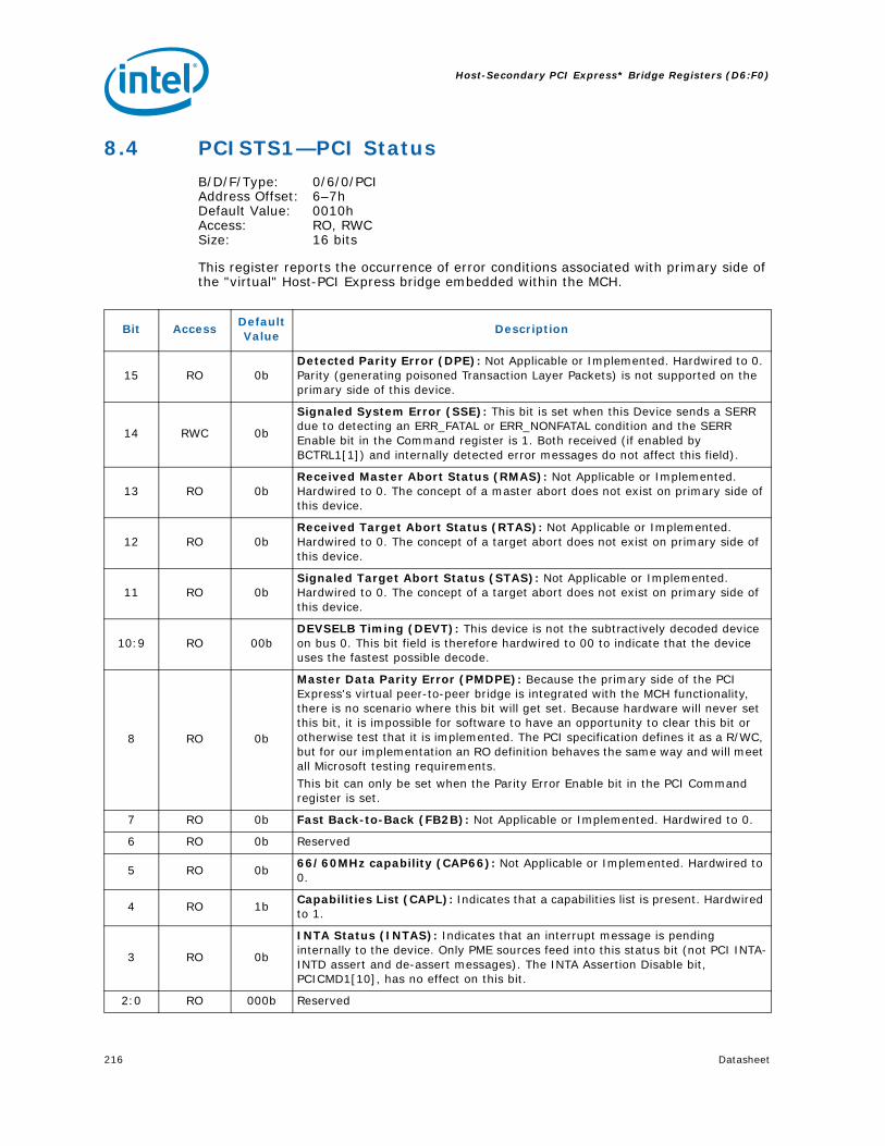
Host-Secondary PCI Express* Bridge Registers (D6:F0)
216 Datasheet
8.4 PCISTS1—PCI Status
B/D/F/Type: 0/6/0/PCIAddress Offset: 6–7hDefault Value: 0010hAccess: RO, RWC Size: 16 bits
This register reports the occurrence of error conditions associated with primary side of the "virtual" Host-PCI Express bridge embedded within the MCH.
Bit AccessDefault Value
Description
15 RO 0bDetected Parity Error (DPE): Not Applicable or Implemented. Hardwired to 0. Parity (generating poisoned Transaction Layer Packets) is not supported on the primary side of this device.
14 RWC 0b
Signaled System Error (SSE): This bit is set when this Device sends a SERR due to detecting an ERR_FATAL or ERR_NONFATAL condition and the SERR Enable bit in the Command register is 1. Both received (if enabled by BCTRL1[1]) and internally detected error messages do not affect this field).
13 RO 0bReceived Master Abort Status (RMAS): Not Applicable or Implemented. Hardwired to 0. The concept of a master abort does not exist on primary side of this device.
12 RO 0bReceived Target Abort Status (RTAS): Not Applicable or Implemented. Hardwired to 0. The concept of a target abort does not exist on primary side of this device.
11 RO 0bSignaled Target Abort Status (STAS): Not Applicable or Implemented. Hardwired to 0. The concept of a target abort does not exist on primary side of this device.
10:9 RO 00bDEVSELB Timing (DEVT): This device is not the subtractively decoded device on bus 0. This bit field is therefore hardwired to 00 to indicate that the device uses the fastest possible decode.
8 RO 0b
Master Data Parity Error (PMDPE): Because the primary side of the PCI Express's virtual peer-to-peer bridge is integrated with the MCH functionality, there is no scenario where this bit will get set. Because hardware will never set this bit, it is impossible for software to have an opportunity to clear this bit or otherwise test that it is implemented. The PCI specification defines it as a R/WC, but for our implementation an RO definition behaves the same way and will meet all Microsoft testing requirements. This bit can only be set when the Parity Error Enable bit in the PCI Command register is set.
7 RO 0b Fast Back-to-Back (FB2B): Not Applicable or Implemented. Hardwired to 0.
6 RO 0b Reserved
5 RO 0b66/60MHz capability (CAP66): Not Applicable or Implemented. Hardwired to 0.
4 RO 1bCapabilities List (CAPL): Indicates that a capabilities list is present. Hardwired to 1.
3 RO 0b
INTA Status (INTAS): Indicates that an interrupt message is pending internally to the device. Only PME sources feed into this status bit (not PCI INTA-INTD assert and de-assert messages). The INTA Assertion Disable bit, PCICMD1[10], has no effect on this bit.
2:0 RO 000b Reserved
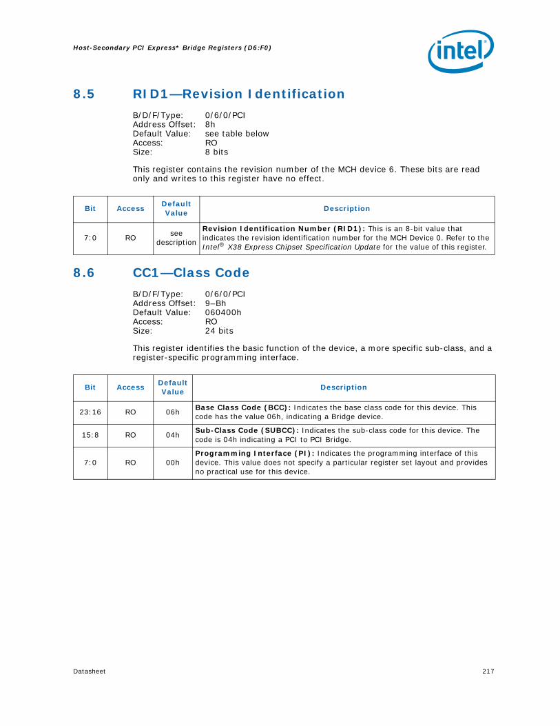
Datasheet 217
Host-Secondary PCI Express* Bridge Registers (D6:F0)
8.5 RID1—Revision Identification
B/D/F/Type: 0/6/0/PCIAddress Offset: 8hDefault Value: see table belowAccess: RO Size: 8 bits
This register contains the revision number of the MCH device 6. These bits are read only and writes to this register have no effect.
8.6 CC1—Class Code
B/D/F/Type: 0/6/0/PCIAddress Offset: 9–BhDefault Value: 060400hAccess: RO Size: 24 bits
This register identifies the basic function of the device, a more specific sub-class, and a register-specific programming interface.
Bit AccessDefault Value
Description
7:0 ROsee
description
Revision Identification Number (RID1): This is an 8-bit value that indicates the revision identification number for the MCH Device 0. Refer to the Intel® X38 Express Chipset Specification Update for the value of this register.
Bit AccessDefault Value
Description
23:16 RO 06hBase Class Code (BCC): Indicates the base class code for this device. This code has the value 06h, indicating a Bridge device.
15:8 RO 04hSub-Class Code (SUBCC): Indicates the sub-class code for this device. The code is 04h indicating a PCI to PCI Bridge.
7:0 RO 00hProgramming Interface (PI): Indicates the programming interface of this device. This value does not specify a particular register set layout and provides no practical use for this device.

Host-Secondary PCI Express* Bridge Registers (D6:F0)
218 Datasheet
8.7 CL1—Cache Line Size
B/D/F/Type: 0/6/0/PCIAddress Offset: ChDefault Value: 00hAccess: RW Size: 8 bits
8.8 HDR1—Header Type
B/D/F/Type: 0/6/0/PCIAddress Offset: EhDefault Value: 01hAccess: RO Size: 8 bits
This register identifies the header layout of the configuration space. No physical register exists at this location.
8.9 PBUSN1—Primary Bus Number
B/D/F/Type: 0/6/0/PCIAddress Offset: 18hDefault Value: 00hAccess: RO Size: 8 bits
This register identifies that this "virtual" Host-PCI Express bridge is connected to PCI bus #0.
Bit AccessDefault Value
Description
7:0 RW 00hCache Line Size (Scratch pad): Implemented by PCI Express devices as a read-write field for legacy compatibility purposes but has no impact on any PCI Express device functionality.
Bit AccessDefault Value
Description
7:0 RO 01hHeader Type Register (HDR): Returns 01h to indicate that this is a single function device with bridge header layout.
Bit AccessDefault Value
Description
7:0 RO 00h
Primary Bus Number (BUSN): Configuration software typically programs this field with the number of the bus on the primary side of the bridge. Since device #6 is an internal device and its primary bus is always 0, these bits are read only and are hardwired to 0.

Datasheet 219
Host-Secondary PCI Express* Bridge Registers (D6:F0)
8.10 SBUSN1—Secondary Bus Number
B/D/F/Type: 0/6/0/PCIAddress Offset: 19hDefault Value: 00hAccess: RW Size: 8 bits
This register identifies the bus number assigned to the second bus side of the "virtual" bridge. This number is programmed by the PCI configuration software to allow mapping of configuration cycles to PCI Express.
8.11 SUBUSN1—Subordinate Bus Number
B/D/F/Type: 0/6/0/PCIAddress Offset: 1AhDefault Value: 00hAccess: RW Size: 8 bits
This register identifies the subordinate bus (if any) that resides at the level below PCI Express. This number is programmed by the PCI configuration software to allow mapping of configuration cycles to PCI Express.
Bit AccessDefault Value
Description
7:0 RW 00hSecondary Bus Number (BUSN): This field is programmed by configuration software with the bus number assigned to PCI Express.
Bit AccessDefault Value
Description
7:0 RW 00h
Subordinate Bus Number (BUSN): This register is programmed by configuration software with the number of the highest subordinate bus that lies behind the device #6 bridge. When only a single PCI device resides on the PCI Express segment, this register will contain the same value as the SBUSN1 register.
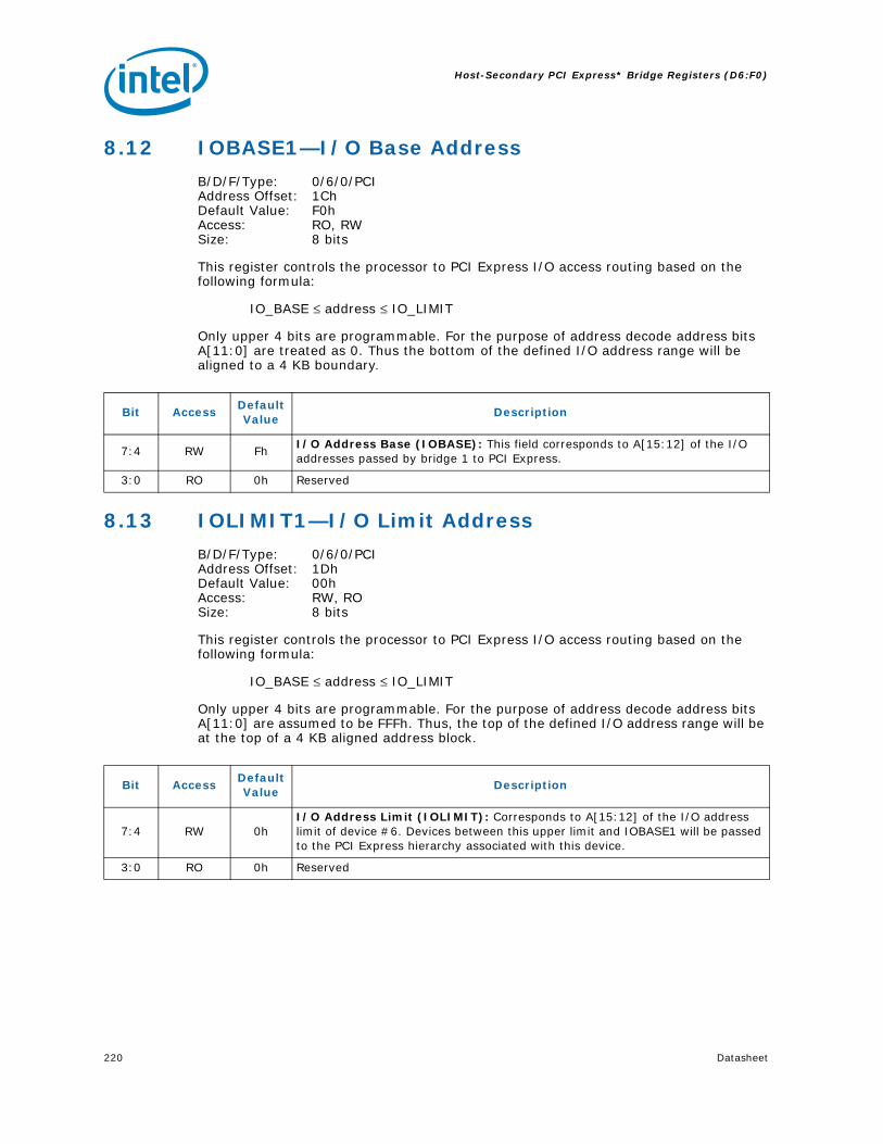
Host-Secondary PCI Express* Bridge Registers (D6:F0)
220 Datasheet
8.12 IOBASE1—I/O Base Address
B/D/F/Type: 0/6/0/PCIAddress Offset: 1ChDefault Value: F0hAccess: RO, RW Size: 8 bits
This register controls the processor to PCI Express I/O access routing based on the following formula:
IO_BASE ≤ address ≤ IO_LIMIT
Only upper 4 bits are programmable. For the purpose of address decode address bits A[11:0] are treated as 0. Thus the bottom of the defined I/O address range will be aligned to a 4 KB boundary.
8.13 IOLIMIT1—I/O Limit Address
B/D/F/Type: 0/6/0/PCIAddress Offset: 1DhDefault Value: 00hAccess: RW, RO Size: 8 bits
This register controls the processor to PCI Express I/O access routing based on the following formula:
IO_BASE ≤ address ≤ IO_LIMIT
Only upper 4 bits are programmable. For the purpose of address decode address bits A[11:0] are assumed to be FFFh. Thus, the top of the defined I/O address range will be at the top of a 4 KB aligned address block.
Bit AccessDefault Value
Description
7:4 RW FhI/O Address Base (IOBASE): This field corresponds to A[15:12] of the I/O addresses passed by bridge 1 to PCI Express.
3:0 RO 0h Reserved
Bit AccessDefault Value
Description
7:4 RW 0hI/O Address Limit (IOLIMIT): Corresponds to A[15:12] of the I/O address limit of device #6. Devices between this upper limit and IOBASE1 will be passed to the PCI Express hierarchy associated with this device.
3:0 RO 0h Reserved

Datasheet 221
Host-Secondary PCI Express* Bridge Registers (D6:F0)
8.14 SSTS1—Secondary Status
B/D/F/Type: 0/6/0/PCIAddress Offset: 1E–1FhDefault Value: 0000hAccess: RO, RWC Size: 16 bits
SSTS1 is a 16-bit status register that reports the occurrence of error conditions associated with secondary side of the "virtual" PCI-PCI bridge embedded within MCH.
Bit AccessDefault Value
Description
15 RWC 0b
Detected Parity Error (DPE): This bit is set by the Secondary Side for a Type 1 Configuration Space header device whenever it receives a Poisoned Transaction Layer Packet, regardless of the state of the Parity Error Response Enable bit in the Bridge Control Register.
14 RWC 0bReceived System Error (RSE): This bit is set when the Secondary Side for a Type 1 configuration space header device receives an ERR_FATAL or ERR_NONFATAL.
13 RWC 0b
Received Master Abort (RMA): This bit is set when the Secondary Side for Type 1 Configuration Space Header Device (for requests initiated by the Type 1 Header Device itself) receives a Completion with Unsupported Request Completion Status.
12 RWC 0b
Received Target Abort (RTA): This bit is set when the Secondary Side for Type 1 Configuration Space Header Device (for requests initiated by the Type 1 Header Device itself) receives a Completion with Completer Abort Completion Status.
11 RO 0bSignaled Target Abort (STA): Not Applicable or Implemented. Hardwired to 0. The MCH does not generate Target Aborts (the MCH will never complete a request using the Completer Abort Completion status).
10:9 RO 00b DEVSELB Timing (DEVT): Not Applicable or Implemented. Hardwired to 0.
8 RWC 0b
Master Data Parity Error (SMDPE): When set, indicates that the MCH received across the link (upstream) a Read Data Completion Poisoned Transaction Layer Packet (EP=1). This bit can only be set when the Parity Error Enable bit in the Bridge Control register is set.
7 RO 0b Fast Back-to-Back (FB2B): Not Applicable or Implemented. Hardwired to 0.
6 RO 0b Reserved
5 RO 0b66/60 MHz capability (CAP66): Not Applicable or Implemented. Hardwired to 0.
4:0 RO 00h Reserved

Host-Secondary PCI Express* Bridge Registers (D6:F0)
222 Datasheet
8.15 MBASE1—Memory Base Address
B/D/F/Type: 0/6/0/PCIAddress Offset: 20–21hDefault Value: FFF0hAccess: RW, RO Size: 16 bits
This register controls the processor to PCI Express non-prefetchable memory access routing based on the following formula:
MEMORY_BASE ≤ address ≤ MEMORY_LIMIT
The upper 12 bits of the register are read/write and correspond to the upper 12 address bits A[31:20] of the 32 bit address. The bottom 4 bits of this register are read-only and return zeroes when read. This register must be initialized by the configuration software. For the purpose of address decode address bits A[19:0] are assumed to be 0. Thus, the bottom of the defined memory address range will be aligned to a 1 MB boundary.
Bit AccessDefault Value
Description
15:4 RW FFFhMemory Address Base (MBASE): Corresponds to A[31:20] of the lower limit of the memory range that will be passed to PCI Express.
3:0 RO 0h Reserved
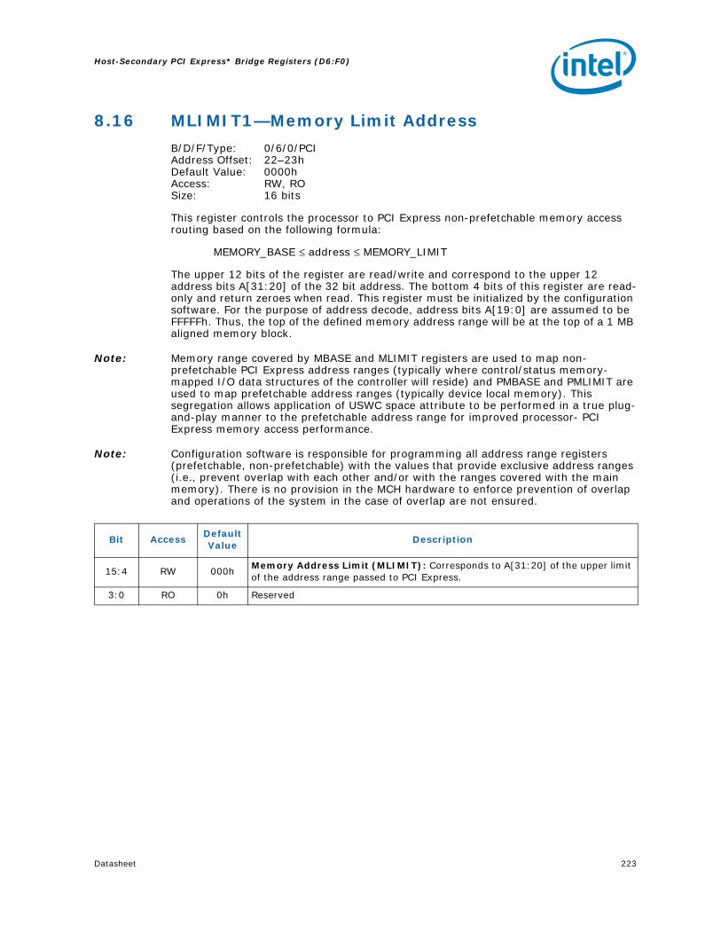
Datasheet 223
Host-Secondary PCI Express* Bridge Registers (D6:F0)
8.16 MLIMIT1—Memory Limit Address
B/D/F/Type: 0/6/0/PCIAddress Offset: 22–23hDefault Value: 0000hAccess: RW, RO Size: 16 bits
This register controls the processor to PCI Express non-prefetchable memory access routing based on the following formula:
MEMORY_BASE ≤ address ≤ MEMORY_LIMIT
The upper 12 bits of the register are read/write and correspond to the upper 12 address bits A[31:20] of the 32 bit address. The bottom 4 bits of this register are read-only and return zeroes when read. This register must be initialized by the configuration software. For the purpose of address decode, address bits A[19:0] are assumed to be FFFFFh. Thus, the top of the defined memory address range will be at the top of a 1 MB aligned memory block.
Note: Memory range covered by MBASE and MLIMIT registers are used to map non-prefetchable PCI Express address ranges (typically where control/status memory-mapped I/O data structures of the controller will reside) and PMBASE and PMLIMIT are used to map prefetchable address ranges (typically device local memory). This segregation allows application of USWC space attribute to be performed in a true plug-and-play manner to the prefetchable address range for improved processor- PCI Express memory access performance.
Note: Configuration software is responsible for programming all address range registers (prefetchable, non-prefetchable) with the values that provide exclusive address ranges (i.e., prevent overlap with each other and/or with the ranges covered with the main memory). There is no provision in the MCH hardware to enforce prevention of overlap and operations of the system in the case of overlap are not ensured.
Bit AccessDefault Value
Description
15:4 RW 000hMemory Address Limit (MLIMIT): Corresponds to A[31:20] of the upper limit of the address range passed to PCI Express.
3:0 RO 0h Reserved

Host-Secondary PCI Express* Bridge Registers (D6:F0)
224 Datasheet
8.17 PMBASE1—Prefetchable Memory Base Address Upper
B/D/F/Type: 0/6/0/PCIAddress Offset: 24–25hDefault Value: FFF1hAccess: RW, RO Size: 16 bits
This register in conjunction with the corresponding Upper Base Address register controls the processor to PCI Express prefetchable memory access routing based on the following formula:
PREFETCHABLE_MEMORY_BASE ≤ address ≤ PREFETCHABLE_MEMORY_LIMIT
The upper 12 bits of this register are read/write and correspond to address bits A[31:20] of the 40-bit address. The lower 8 bits of the Upper Base Address register are read/write and correspond to address bits A[39:32] of the 40-bit address. This register must be initialized by the configuration software. For the purpose of address decode, address bits A[19:0] are assumed to be 0. Thus, the bottom of the defined memory address range will be aligned to a 1 MB boundary.
Bit AccessDefault Value
Description
15:4 RW FFFhPrefetchable Memory Base Address (MBASE): Corresponds to A[31:20] of the lower limit of the memory range that will be passed to PCI Express.
3:0 RO 1h64-bit Address Support: Indicates that the upper 32 bits of the prefetchable memory region base address are contained in the Prefetchable Memory base Upper Address register at 28h.
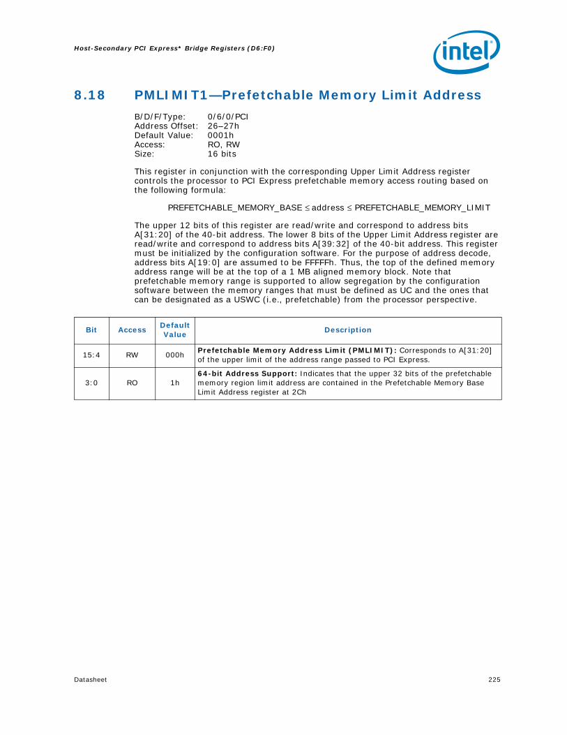
Datasheet 225
Host-Secondary PCI Express* Bridge Registers (D6:F0)
8.18 PMLIMIT1—Prefetchable Memory Limit Address
B/D/F/Type: 0/6/0/PCIAddress Offset: 26–27hDefault Value: 0001hAccess: RO, RW Size: 16 bits
This register in conjunction with the corresponding Upper Limit Address register controls the processor to PCI Express prefetchable memory access routing based on the following formula:
PREFETCHABLE_MEMORY_BASE ≤ address ≤ PREFETCHABLE_MEMORY_LIMIT
The upper 12 bits of this register are read/write and correspond to address bits A[31:20] of the 40-bit address. The lower 8 bits of the Upper Limit Address register are read/write and correspond to address bits A[39:32] of the 40-bit address. This register must be initialized by the configuration software. For the purpose of address decode, address bits A[19:0] are assumed to be FFFFFh. Thus, the top of the defined memory address range will be at the top of a 1 MB aligned memory block. Note that prefetchable memory range is supported to allow segregation by the configuration software between the memory ranges that must be defined as UC and the ones that can be designated as a USWC (i.e., prefetchable) from the processor perspective.
Bit AccessDefault Value
Description
15:4 RW 000hPrefetchable Memory Address Limit (PMLIMIT): Corresponds to A[31:20] of the upper limit of the address range passed to PCI Express.
3:0 RO 1h64-bit Address Support: Indicates that the upper 32 bits of the prefetchable memory region limit address are contained in the Prefetchable Memory Base Limit Address register at 2Ch

Host-Secondary PCI Express* Bridge Registers (D6:F0)
226 Datasheet
8.19 PMBASEU1—Prefetchable Memory Base Address Upper
B/D/F/Type: 0/6/0/PCIAddress Offset: 28–2BhDefault Value: 00000000hAccess: RW Size: 32 bits
The functionality associated with this register is present in the PCI Express design implementation.
This register in conjunction with the corresponding Upper Base Address register controls the processor to PCI Express prefetchable memory access routing based on the following formula:
PREFETCHABLE_MEMORY_BASE ≤ address ≤ PREFETCHABLE_MEMORY_LIMIT
The upper 12 bits of this register are read/write and correspond to address bits A[31:20] of the 40-bit address. The lower 8 bits of the Upper Base Address register are read/write and correspond to address bits A[39:32] of the 40-bit address. This register must be initialized by the configuration software. For the purpose of address decode, address bits A[19:0] are assumed to be 0. Thus, the bottom of the defined memory address range will be aligned to a 1 MB boundary.
Bit AccessDefault Value
Description
31:0 RW0000000
0h
Prefetchable Memory Base Address (MBASEU): Corresponds to A[63:32] of the lower limit of the prefetchable memory range that will be passed to PCI Express.
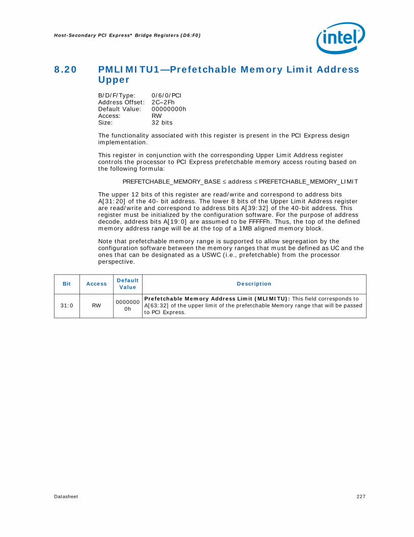
Datasheet 227
Host-Secondary PCI Express* Bridge Registers (D6:F0)
8.20 PMLIMITU1—Prefetchable Memory Limit Address Upper
B/D/F/Type: 0/6/0/PCIAddress Offset: 2C–2FhDefault Value: 00000000hAccess: RW Size: 32 bits
The functionality associated with this register is present in the PCI Express design implementation.
This register in conjunction with the corresponding Upper Limit Address register controls the processor to PCI Express prefetchable memory access routing based on the following formula:
PREFETCHABLE_MEMORY_BASE ≤ address ≤ PREFETCHABLE_MEMORY_LIMIT
The upper 12 bits of this register are read/write and correspond to address bits A[31:20] of the 40- bit address. The lower 8 bits of the Upper Limit Address register are read/write and correspond to address bits A[39:32] of the 40-bit address. This register must be initialized by the configuration software. For the purpose of address decode, address bits A[19:0] are assumed to be FFFFFh. Thus, the top of the defined memory address range will be at the top of a 1MB aligned memory block.
Note that prefetchable memory range is supported to allow segregation by the configuration software between the memory ranges that must be defined as UC and the ones that can be designated as a USWC (i.e., prefetchable) from the processor perspective.
Bit AccessDefault Value
Description
31:0 RW0000000
0h
Prefetchable Memory Address Limit (MLIMITU): This field corresponds to A[63:32] of the upper limit of the prefetchable Memory range that will be passed to PCI Express.
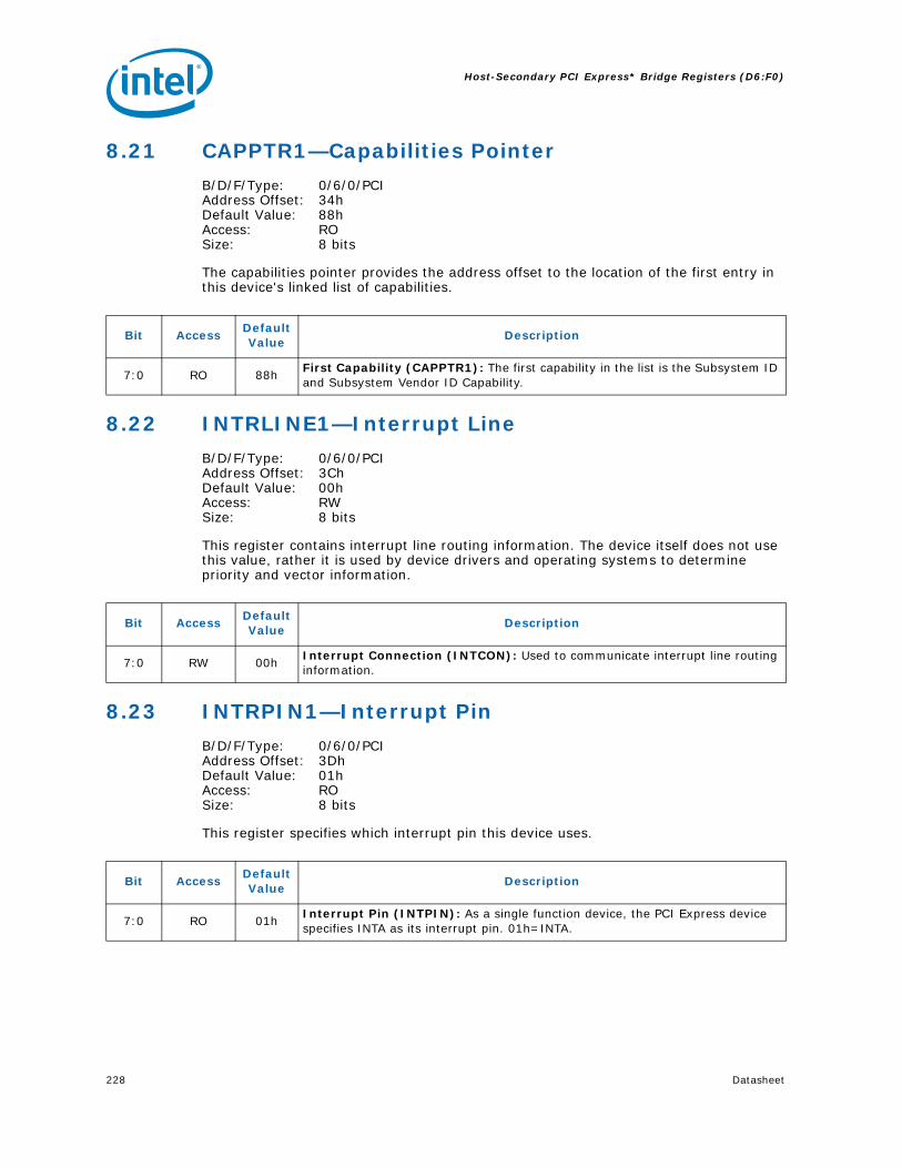
Host-Secondary PCI Express* Bridge Registers (D6:F0)
228 Datasheet
8.21 CAPPTR1—Capabilities Pointer
B/D/F/Type: 0/6/0/PCIAddress Offset: 34hDefault Value: 88hAccess: RO Size: 8 bits
The capabilities pointer provides the address offset to the location of the first entry in this device's linked list of capabilities.
8.22 INTRLINE1—Interrupt Line
B/D/F/Type: 0/6/0/PCIAddress Offset: 3ChDefault Value: 00hAccess: RW Size: 8 bits
This register contains interrupt line routing information. The device itself does not use this value, rather it is used by device drivers and operating systems to determine priority and vector information.
8.23 INTRPIN1—Interrupt Pin
B/D/F/Type: 0/6/0/PCIAddress Offset: 3DhDefault Value: 01hAccess: RO Size: 8 bits
This register specifies which interrupt pin this device uses.
Bit AccessDefault Value
Description
7:0 RO 88hFirst Capability (CAPPTR1): The first capability in the list is the Subsystem ID and Subsystem Vendor ID Capability.
Bit AccessDefault Value
Description
7:0 RW 00hInterrupt Connection (INTCON): Used to communicate interrupt line routing information.
Bit AccessDefault Value
Description
7:0 RO 01hInterrupt Pin (INTPIN): As a single function device, the PCI Express device specifies INTA as its interrupt pin. 01h=INTA.
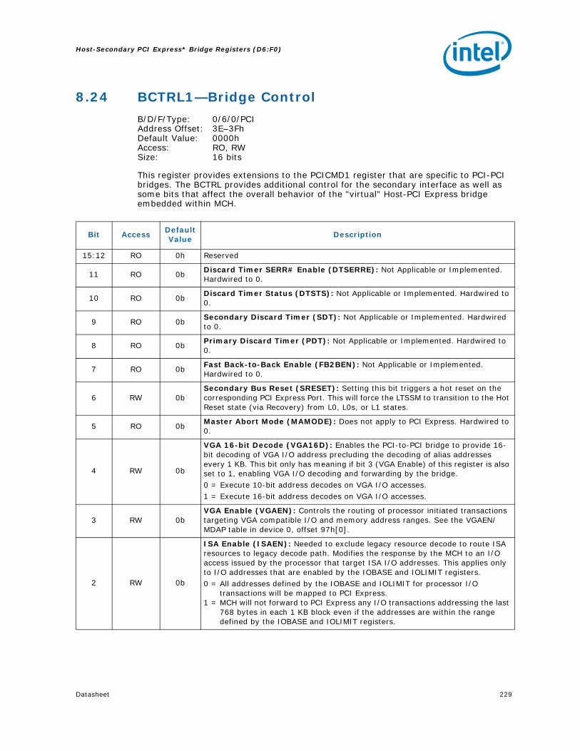
Datasheet 229
Host-Secondary PCI Express* Bridge Registers (D6:F0)
8.24 BCTRL1—Bridge Control
B/D/F/Type: 0/6/0/PCIAddress Offset: 3E–3FhDefault Value: 0000hAccess: RO, RW Size: 16 bits
This register provides extensions to the PCICMD1 register that are specific to PCI-PCI bridges. The BCTRL provides additional control for the secondary interface as well as some bits that affect the overall behavior of the "virtual" Host-PCI Express bridge embedded within MCH.
Bit AccessDefault Value
Description
15:12 RO 0h Reserved
11 RO 0bDiscard Timer SERR# Enable (DTSERRE): Not Applicable or Implemented. Hardwired to 0.
10 RO 0bDiscard Timer Status (DTSTS): Not Applicable or Implemented. Hardwired to 0.
9 RO 0bSecondary Discard Timer (SDT): Not Applicable or Implemented. Hardwired to 0.
8 RO 0bPrimary Discard Timer (PDT): Not Applicable or Implemented. Hardwired to 0.
7 RO 0bFast Back-to-Back Enable (FB2BEN): Not Applicable or Implemented. Hardwired to 0.
6 RW 0bSecondary Bus Reset (SRESET): Setting this bit triggers a hot reset on the corresponding PCI Express Port. This will force the LTSSM to transition to the Hot Reset state (via Recovery) from L0, L0s, or L1 states.
5 RO 0bMaster Abort Mode (MAMODE): Does not apply to PCI Express. Hardwired to 0.
4 RW 0b
VGA 16-bit Decode (VGA16D): Enables the PCI-to-PCI bridge to provide 16-bit decoding of VGA I/O address precluding the decoding of alias addresses every 1 KB. This bit only has meaning if bit 3 (VGA Enable) of this register is also set to 1, enabling VGA I/O decoding and forwarding by the bridge.0 = Execute 10-bit address decodes on VGA I/O accesses.1 = Execute 16-bit address decodes on VGA I/O accesses.
3 RW 0bVGA Enable (VGAEN): Controls the routing of processor initiated transactions targeting VGA compatible I/O and memory address ranges. See the VGAEN/MDAP table in device 0, offset 97h[0].
2 RW 0b
ISA Enable (ISAEN): Needed to exclude legacy resource decode to route ISA resources to legacy decode path. Modifies the response by the MCH to an I/O access issued by the processor that target ISA I/O addresses. This applies only to I/O addresses that are enabled by the IOBASE and IOLIMIT registers. 0 = All addresses defined by the IOBASE and IOLIMIT for processor I/O
transactions will be mapped to PCI Express. 1 = MCH will not forward to PCI Express any I/O transactions addressing the last
768 bytes in each 1 KB block even if the addresses are within the range defined by the IOBASE and IOLIMIT registers.

Host-Secondary PCI Express* Bridge Registers (D6:F0)
230 Datasheet
8.25 PM_CAPID1—Power Management Capabilities
B/D/F/Type: 0/6/0/PCIAddress Offset: 80–83hDefault Value: C8039001hAccess: RO Size: 32 bits
1 RW 0b
SERR Enable (SERREN): 0 = No forwarding of error messages from secondary side to primary side that
could result in an SERR.1 = ERR_COR, ERR_NONFATAL, and ERR_FATAL messages result in SERR
message when individually enabled by the Root Control register.
0 RW 0b
Parity Error Response Enable (PEREN): Controls whether or not the Master Data Parity Error bit in the Secondary Status register is set when the MCH receives across the link (upstream) a Read Data Completion Poisoned Transaction Layer Packet.0 = Master Data Parity Error bit in Secondary Status register can NOT be set.1 = Master Data Parity Error bit in Secondary Status register CAN be set.
Bit AccessDefault Value
Description
Bit AccessDefault Value
Description
31:27 RO 19h
PME Support (PMES): This field indicates the power states in which this device may indicate PME wake via PCI Express messaging. D0, D3hot & D3cold. This device is not required to do anything to support D3hot and D3cold, it simply must report that those states are supported. Refer to the PCI Power Management 1.1 specification for encoding explanation and other power management details.
26 RO 0bD2 Power State Support (D2PSS): Hardwired to 0 to indicate that the D2 power management state is NOT supported.
25 RO 0bD1 Power State Support (D1PSS): Hardwired to 0 to indicate that the D1 power management state is NOT supported.
24:22 RO 000bAuxiliary Current (AUXC): Hardwired to 0 to indicate that there are no 3.3Vaux auxiliary current requirements.
21 RO 0bDevice Specific Initialization (DSI): Hardwired to 0 to indicate that special initialization of this device is NOT required before generic class device driver is to use it.
20 RO 0b Auxiliary Power Source (APS): Hardwired to 0.
19 RO 0bPME Clock (PMECLK): Hardwired to 0 to indicate this device does NOT support PMEB generation.
18:16 RO 011bPCI PM CAP Version (PCIPMCV): A value of 011b indicates that this function complies with revision 1.2 of the PCI Power Management Interface Specification.
15:8 RO 90hPointer to Next Capability (PNC): This contains a pointer to the next item in the capabilities list. If MSICH (CAPL[0] @ 7Fh) is 0, then the next item in the capabilities list is the Message Signaled Interrupts (MSI) capability at 90h.
7:0 RO 01hCapability ID (CID): Value of 01h identifies this linked list item (capability structure) as being for PCI Power Management registers.

Datasheet 231
Host-Secondary PCI Express* Bridge Registers (D6:F0)
8.26 PM_CS1—Power Management Control/Status
B/D/F/Type: 0/6/0/PCIAddress Offset: 84–87hDefault Value: 00000008hAccess: RO, RW, RW/P Size: 32 bits
Bit AccessDefault Value
Description
31:16 RO 0000h Reserved
15 RO 0bPME Status (PMESTS): Indicates that this device does not support PMEB generation from D3cold.
14:13 RO 00bData Scale (DSCALE): Indicates that this device does not support the power management data register.
12:9 RO 0hData Select (DSEL): Indicates that this device does not support the power management data register.
8 RW/P 0b
PME Enable (PMEE): Indicates that this device does not generate PMEB assertion from any D-state.0 = PMEB generation not possible from any D State1 = PMEB generation enabled from any D StateThe setting of this bit has no effect on hardware.See PM_CAP[15:11]
7:2 RO 0000b Reserved
1:0 RW 00b
Power State (PS): Indicates the current power state of this device and can be used to set the device into a new power state. If software attempts to write an unsupported state to this field, write operation must complete normally on the bus, but the data is discarded and no state change occurs.00 = D001 = D1 (Not supported in this device.)10 = D2 (Not supported in this device.)11 = D3Support of D3cold does not require any special action. While in the D3hot state, this device can only act as the target of PCI configuration transactions (for power management control). This device also cannot generate interrupts or respond to MMR cycles in the D3 state. The device must return to the D0 state in order to be fully-functional. When the Power State is other than D0, the bridge will Master Abort (i.e. not claim) any downstream cycles (with exception of type 0 config cycles). Consequently, these unclaimed cycles will go down DMI and come back up as Unsupported Requests, which the MCH logs as Master Aborts in Device 0 PCISTS[13]There is no additional hardware functionality required to support these Power States.
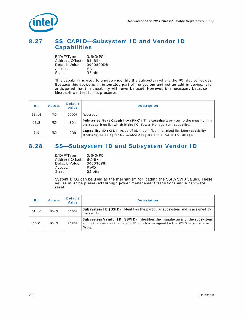
Host-Secondary PCI Express* Bridge Registers (D6:F0)
232 Datasheet
8.27 SS_CAPID—Subsystem ID and Vendor ID Capabilities
B/D/F/Type: 0/6/0/PCIAddress Offset: 88–8BhDefault Value: 0000800DhAccess: RO Size: 32 bits
This capability is used to uniquely identify the subsystem where the PCI device resides. Because this device is an integrated part of the system and not an add-in device, it is anticipated that this capability will never be used. However, it is necessary because Microsoft will test for its presence.
8.28 SS—Subsystem ID and Subsystem Vendor ID
B/D/F/Type: 0/6/0/PCIAddress Offset: 8C–8FhDefault Value: 00008086hAccess: RWO Size: 32 bits
System BIOS can be used as the mechanism for loading the SSID/SVID values. These values must be preserved through power management transitions and a hardware reset.
Bit AccessDefault Value
Description
31:16 RO 0000h Reserved
15:8 RO 80hPointer to Next Capability (PNC): This contains a pointer to the next item in the capabilities list which is the PCI Power Management capability.
7:0 RO 0DhCapability ID (CID): Value of 0Dh identifies this linked list item (capability structure) as being for SSID/SSVID registers in a PCI-to-PCI Bridge.
Bit AccessDefault Value
Description
31:16 RWO 0000hSubsystem ID (SSID): Identifies the particular subsystem and is assigned by the vendor.
15:0 RWO 8086hSubsystem Vendor ID (SSVID): Identifies the manufacturer of the subsystem and is the same as the vendor ID which is assigned by the PCI Special Interest Group.

Datasheet 233
Host-Secondary PCI Express* Bridge Registers (D6:F0)
8.29 MSI_CAPID—Message Signaled Interrupts Capability ID
B/D/F/Type: 0/6/0/PCIAddress Offset: 90–91hDefault Value: A005hAccess: RO Size: 16 bits
When a device supports MSI, it can generate an interrupt request to the processor by writing a predefined data item (a message) to a predefined memory address.
8.30 MC—Message Control
B/D/F/Type: 0/6/0/PCIAddress Offset: 92–93hDefault Value: 0000hAccess: RW, RO Size: 16 bits
System software can modify bits in this register, but the device is prohibited from doing so.
If the device writes the same message multiple times, only one of those messages is guaranteed to be serviced. If all of them must be serviced, the device must not generate the same message again until the driver services the earlier one.
Bit AccessDefault Value
Description
15:8 RO A0hPointer to Next Capability (PNC): This contains a pointer to the next item in the capabilities list which is the PCI Express capability.
7:0 RO 05hCapability ID (CID): Value of 05h identifies this linked list item (capability structure) as being for MSI registers.
Bit AccessDefault Value
Description
15:8 RO 00h Reserved
7 RO 0b64-bit Address Capable (64AC): Hardwired to 0 to indicate that the function does not implement the upper 32 bits of the Message Address register and is incapable of generating a 64-bit memory address.
6:4 RW 000b
Multiple Message Enable (MME): System software programs this field to indicate the actual number of messages allocated to this device. This number will be equal to or less than the number actually requested. The encoding is the same as for the MMC field below.
3:1 RO 000b
Multiple Message Capable (MMC): System software reads this field to determine the number of messages being requested by this device. The value of 000b equates to 1 message requested.000 = 1 message requestedAll other encodings are reserved.
0 RW 0b
MSI Enable (MSIEN): Controls the ability of this device to generate MSIs. 0 = MSI will not be generated. 1 = MSI will be generated when we receive PME messages. INTA will not be
generated and INTA Status (PCISTS1[3]) will not be set.
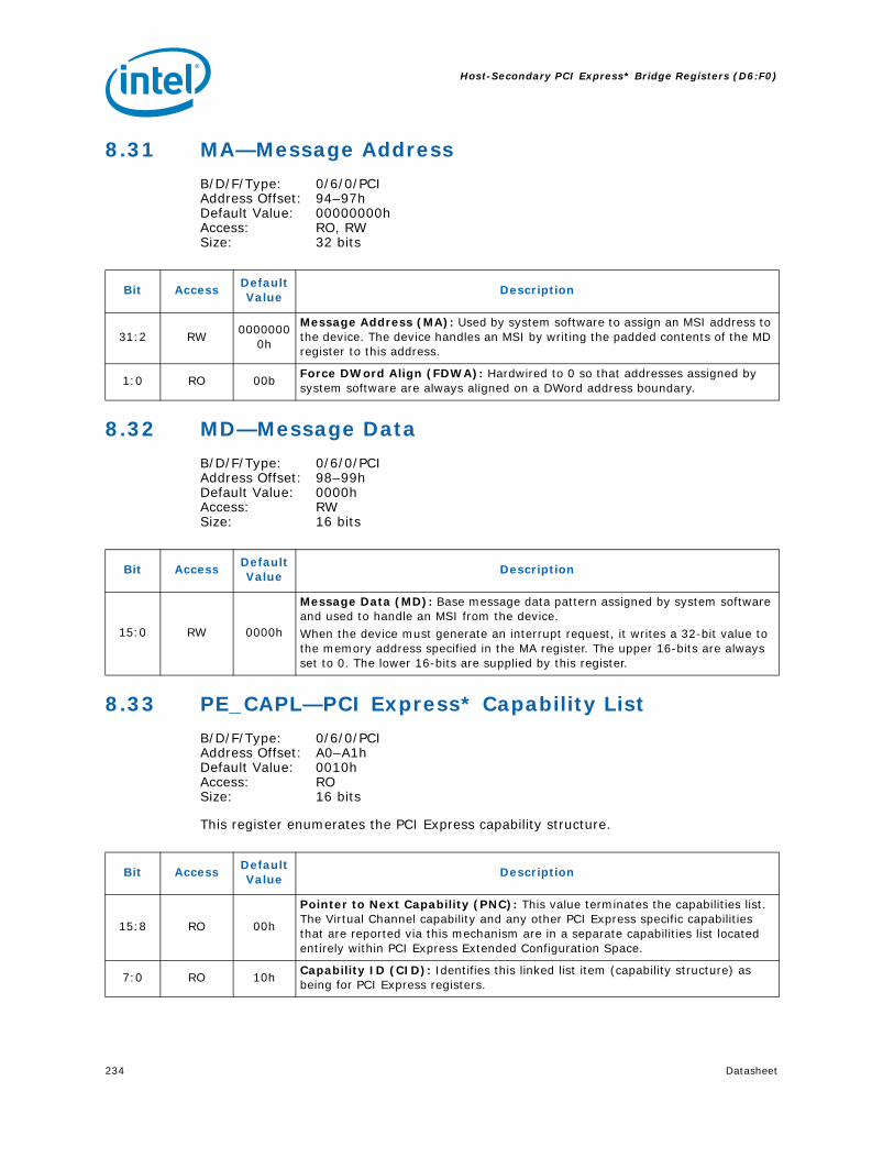
Host-Secondary PCI Express* Bridge Registers (D6:F0)
234 Datasheet
8.31 MA—Message Address
B/D/F/Type: 0/6/0/PCIAddress Offset: 94–97hDefault Value: 00000000hAccess: RO, RW Size: 32 bits
8.32 MD—Message Data
B/D/F/Type: 0/6/0/PCIAddress Offset: 98–99hDefault Value: 0000hAccess: RW Size: 16 bits
8.33 PE_CAPL—PCI Express* Capability List
B/D/F/Type: 0/6/0/PCIAddress Offset: A0–A1hDefault Value: 0010hAccess: RO Size: 16 bits
This register enumerates the PCI Express capability structure.
Bit AccessDefault Value
Description
31:2 RW0000000
0h
Message Address (MA): Used by system software to assign an MSI address to the device. The device handles an MSI by writing the padded contents of the MD register to this address.
1:0 RO 00bForce DWord Align (FDWA): Hardwired to 0 so that addresses assigned by system software are always aligned on a DWord address boundary.
Bit AccessDefault Value
Description
15:0 RW 0000h
Message Data (MD): Base message data pattern assigned by system software and used to handle an MSI from the device. When the device must generate an interrupt request, it writes a 32-bit value to the memory address specified in the MA register. The upper 16-bits are always set to 0. The lower 16-bits are supplied by this register.
Bit AccessDefault Value
Description
15:8 RO 00h
Pointer to Next Capability (PNC): This value terminates the capabilities list. The Virtual Channel capability and any other PCI Express specific capabilities that are reported via this mechanism are in a separate capabilities list located entirely within PCI Express Extended Configuration Space.
7:0 RO 10hCapability ID (CID): Identifies this linked list item (capability structure) as being for PCI Express registers.

Datasheet 235
Host-Secondary PCI Express* Bridge Registers (D6:F0)
8.34 PE_CAP—PCI Express* Capabilities
B/D/F/Type: 0/6/0/PCIAddress Offset: A2–A3hDefault Value: 0142hAccess: RO, RWO Size: 16 bits
This register indicates PCI Express device capabilities.
8.35 DCAP—Device Capabilities
B/D/F/Type: 0/6/0/PCIAddress Offset: A4–A7hDefault Value: 00008000hAccess: RO Size: 32 bits
This register indicates PCI Express device capabilities.
Bit AccessDefault Value
Description
15:14 RO 00b Reserved
13:9 RO 00hInterrupt Message Number (IMN): Not Applicable or Implemented. Hardwired to 0.
8 RWO 1b
Slot Implemented (SI): 0 = The PCI Express Link associated with this port is connected to an integrated
component or is disabled.1 = The PCI Express Link associated with this port is connected to a slot.
7:4 RO 4hDevice/Port Type (DPT): Hardwired to 4h to indicate root port of PCI Express Root Complex.
3:0 RO 2hPCI Express Capability Version (PCIECV): Hardwired to 2h to indicate compliance to the PCI Express Capabilities Register Expansion ECN.
Bit AccessDefault Value
Description
31:16 RO 0000h Reserved
15 RO 1bRole Based Error Reporting (RBER): This bit indicates that this device implements the functionality defined in the Error Reporting ECN as required by the PCI Express 1.1 specification.
14:6 RO 000h Reserved
5 RO 0bExtended Tag Field Supported (ETFS): Hardwired to indicate support for 5-bit Tags as a Requestor.
4:3 RO 00bPhantom Functions Supported (PFS): Not Applicable or Implemented. Hardwired to 0.
2:0 RO 000bMax Payload Size (MPS): Hardwired to indicate 128B max supported payload for Transaction Layer Packets (TLP).

Host-Secondary PCI Express* Bridge Registers (D6:F0)
236 Datasheet
8.36 DCTL—Device Control
B/D/F/Type: 0/6/0/PCIAddress Offset: A8–A9hDefault Value: 0000hAccess: RW, RO Size: 16 bits
This register provides control for PCI Express device specific capabilities.
The error reporting enable bits are in reference to errors detected by this device, not error messages received across the link. The reporting of error messages (ERR_CORR, ERR_NONFATAL, ERR_FATAL) received by Root Port is controlled exclusively by Root Port Command Register.
Bit AccessDefault Value
Description
15:8 RO 0h Reserved
7:5 RW 000b
Max Payload Size (MPS): 000 = 128B max supported payload for Transaction Layer Packets (TLP). As a
receiver, the Device must handle TLPs as large as the set value; as transmitter, the Device must not generate TLPs exceeding the set value.
All other encodings are reserved.Hardware will actually ignore this field. It is writeable only to support compliance testing.
4 RO 0b Reserved
3 RW 0b
Unsupported Request Reporting Enable (URRE): When set, this bit allows signaling ERR_NONFATAL, ERR_FATAL, or ERR_CORR to the Root Control register when detecting an unmasked Unsupported Request (UR). An ERR_CORR is signaled when an unmasked Advisory Non-Fatal UR is received. An ERR_FATAL or ERR_NONFATAL is sent to the Root Control register when an uncorrectable non-Advisory UR is received with the severity bit set in the Uncorrectable Error Severity register.
2 RW 0b
Fatal Error Reporting Enable (FERE): When set, this bit enables signaling of ERR_FATAL to the Root Control register due to internally detected errors or error messages received across the link. Other bits also control the full scope of related error reporting.
1 RW 0b
Non-Fatal Error Reporting Enable (NERE): When set, this bit enables signaling of ERR_NONFATAL to the Rool Control register due to internally detected errors or error messages received across the link. Other bits also control the full scope of related error reporting.
0 RW 0b
Correctable Error Reporting Enable (CERE): When set, this bit enables signaling of ERR_CORR to the Root Control register due to internally detected errors or error messages received across the link. Other bits also control the full scope of related error reporting.

Datasheet 237
Host-Secondary PCI Express* Bridge Registers (D6:F0)
8.37 DSTS—Device Status
B/D/F/Type: 0/6/0/PCIAddress Offset: AA–ABhDefault Value: 0000hAccess: RO, RWC Size: 16 bits
This register reflects status corresponding to controls in the Device Control register. The error reporting bits are in reference to errors detected by this device, not errors messages received across the link.
Bit AccessDefault Value
Description
15:6 RO 000h Reserved
5 RO 0b
Transactions Pending (TP): 0 = All pending transactions (including completions for any outstanding non-
posted requests on any used virtual channel) have been completed.1 = Indicates that the device has transaction(s) pending (including completions
for any outstanding non-posted requests for all used Traffic Classes).
4 RO 0b Reserved
3 RWC 0b
Unsupported Request Detected (URD): When set, this bit indicates that the Device received an Unsupported Request. Errors are logged in this register regardless of whether error reporting is enabled or not in the Device Control Register.Additionally, the Non-Fatal Error Detected bit or the Fatal Error Detected bit is set according to the setting of the Unsupported Request Error Severity bit. In production systems setting the Fatal Error Detected bit is not an option as support for AER will not be reported.
2 RWC 0b
Fatal Error Detected (FED): When set, this bit indicates that fatal error(s) were detected. Errors are logged in this register regardless of whether error reporting is enabled or not in the Device Control register. When Advanced Error Handling is enabled, errors are logged in this register regardless of the settings of the uncorrectable error mask register.
1 RWC 0b
Non-Fatal Error Detected (NFED): When set, this bit indicates that non-fatal error(s) were detected. Errors are logged in this register regardless of whether error reporting is enabled or not in the Device Control register.When Advanced Error Handling is enabled, errors are logged in this register regardless of the settings of the uncorrectable error mask register.
0 RWC 0b
Correctable Error Detected (CED): When set, this bit indicates that correctable error(s) were detected. Errors are logged in this register regardless of whether error reporting is enabled or not in the Device Control register. When Advanced Error Handling is enabled, errors are logged in this register regardless of the settings of the correctable error mask register.

Host-Secondary PCI Express* Bridge Registers (D6:F0)
238 Datasheet
8.38 LCAP—Link Capabilities
B/D/F/Type: 0/6/0/PCIAddress Offset: AC–AFhDefault Value: 03214D02hAccess: RO, RWO Size: 32 bits
This register indicates PCI Express device specific capabilities.
Bit AccessDefault Value
Description
31:24 RO 03hPort Number (PN): This field indicates the PCI Express port number for the given PCI Express link. Matches the value in Element Self Description[31:24].
23:22 RO 000b Reserved
21 RO 1b
Link Bandwidth Notification Capability: A value of 1b indicates support for the Link Bandwidth Notification status and interrupt mechanisms. This capability is required for all Root Ports and Switch downstream ports supporting Links wider than x1 and/or multiple Link speeds.
This field is not applicable and is reserved for Endpoint devices, PCI Express to PCI/PCI-X bridges, and Upstream Ports of Switches.Devices that do not implement the Link Bandwidth Notification capability must hardwire this bit to 0b.
20 RO 0b
Data Link Layer Link Active Reporting Capable (DLLLARC): For a Downstream Port, this bit must be set to 1b if the component supports the optional capability of reporting the DL_Active state of the Data Link Control and Management State Machine. For Upstream Ports and components that do not support this optional capability, this bit must be hardwired to 0b.
19 RO 0b
Surprise Down Error Reporting Capable (SDERC): For a Downstream Port, this bit must be set to 1b if the component supports the optional capability of detecting and reporting a Surprise Down error condition.For Upstream Ports and components that do not support this optional capability, this bit must be hardwired to 0b.
18 RO 0b
Clock Power Management (CPM): A value of 1b in this bit indicates that the component tolerates the removal of any reference clock(s) when the link is in the L1 and L2/3 Ready link states. A value of 0b indicates the component does not have this capability and that reference clock(s) must not be removed in these link states.This capability is applicable only in form factors that support "clock request" (CLKREQ#) capability.For a multi-function device, each function indicates its capability independently. Power Management configuration software must only permit reference clock removal if all functions of the multifunction device indicate a 1b in this bit.
17:15 RWO 010b
L1 Exit Latency (L1ELAT): Indicates the length of time this Port requires to complete the transition from L1 to L0. The value 010 b indicates the range of 2 us to less than 4 us.Both bytes of this register that contain a portion of this field must be written simultaneously in order to prevent an intermediate (and undesired) value from ever existing.

Datasheet 239
Host-Secondary PCI Express* Bridge Registers (D6:F0)
14:12 RO 100b
L0s Exit Latency (L0SELAT): Indicates the length of time this Port requires to complete the transition from L0s to L0.000 = Less than 64 ns001 = 64ns to less than 128ns010 = 128ns to less than 256 ns011 = 256ns to less than 512ns100 = 512ns to less than 1us101 = 1 us to less than 2 us110 = 2 us – 4 us111 = More than 4 us
11:10 RWO 11bActive State Link PM Support (ASLPMS): : The MCH supports ASPM L0s and L1.
9:4 RO 10hMax Link Width (MLW): Indicates the maximum number of lanes supported for this link.10h = x16
3:0 RO 2h
Max Link Speed (MLS): Supported Link Speed - This field indicates the supported Link speed(s) of the associated Port.0001b = 2.5GT/s Link speed supported0010b = 5.0GT/s and 2.5GT/s Link speeds supportedAll other encodings are reserved.
Bit AccessDefault Value
Description

Host-Secondary PCI Express* Bridge Registers (D6:F0)
240 Datasheet
8.39 LCTL—Link Control
B/D/F/Type: 0/6/0/PCIAddress Offset: B0–B1hDefault Value: 0000hAccess: RO, RW, RW/SC Size: 16 bits
This register allows control of PCI Express link.
Bit AccessDefault Value
Description
15:12 RO 0000000b Reserved
11 RW 0b
Link Autonomous Bandwidth Interrupt Enable: When Set, this bit enables the generation of an interrupt to indicate that the Link Autonomous Bandwidth Status bit has been set.This bit is not applicable and is reserved for Endpoint devices, PCI Express to PCI/PCI-X bridges, and Upstream Ports of Switches.Devices that do not implement the Link Bandwidth Notification capability must hardwire this bit to 0b.
10 RW 0b
Link Bandwidth Management Interrupt Enable: When Set, this bit enables the generation of an interrupt to indicate that the Link Bandwidth Management Status bit has been set.This bit is not applicable and is reserved for Endpoint devices, PCI Express to PCI/PCI-X bridges, and Upstream Ports of Switches.
9 R0 0b
Hardware Autonomous Width Disable: When Set, this bit disables hardware from changing the Link width for reasons other than attempting to correct unreliable Link operation by reducing Link width.Devices that do not implement the ability autonomously to change Link width are permitted to hardwire this bit to 0b.The MCH does not support autonomous width change. So, this bit is "RO".
8 RO 0b
Enable Clock Power Management (ECPM): Applicable only for form factors that support a "Clock Request" (CLKREQ#) mechanism, this enable functions as follows:0 = Clock power management is disabled and device must hold CLKREQ#
signal low1 = The device is permitted to use CLKREQ# signal to power manage link clock
according to protocol defined in appropriate form factor specification.Default value of this field is 0b.Components that do not support Clock Power Management (as indicated by a 0b value in the Clock Power Management bit of the Link Capabilities Register) must hardwire this bit to 0b.
7 RW 0b
Extended Synch (ES): 0 = Standard Fast Training Sequence (FTS).1 = Forces the transmission of additional ordered sets when exiting the L0s
state and when in the Recovery state.This mode provides external devices (e.g., logic analyzers) monitoring the Link time to achieve bit and symbol lock before the link enters L0 and resumes communication.This is a test mode only and may cause other undesired side effects such as buffer overflows or underruns.

Datasheet 241
Host-Secondary PCI Express* Bridge Registers (D6:F0)
6 RW 0b
Common Clock Configuration (CCC): 0 = Indicates that this component and the component at the opposite end of
this Link are operating with asynchronous reference clock.1 = Indicates that this component and the component at the opposite end of
this Link are operating with a distributed common reference clock.The state of this bit affects the L0s Exit Latency reported in LCAP[14:12] and the N_FTS value advertised during link training.
5 RW/SC 0b
Retrain Link (RL): 0 = Normal operation.1 = Full Link retraining is initiated by directing the Physical Layer LTSSM from
L0, L0s, or L1 states to the Recovery state.This bit always returns 0 when read.This bit is cleared automatically (no need to write a 0).It is permitted to write 1b to this bit while simultaneously writing modified values to other fields in this register. If the LTSSM is not already in Recovery or Configuration, the resulting Link training must use the modified values. If the LTSSM is already in Recovery or Configuration, the modified values are not required to affect the Link training that's already in progress.
4 RW 0b
Link Disable (LD): 0 = Normal operation.1 = Link is disabled. Forces the LTSSM to transition to the Disabled state (via
Recovery) from L0, L0s, or L1 states. Link retraining happens automatically on 0 to 1 transition, just like when coming out of reset.
Writes to this bit are immediately reflected in the value read from the bit, regardless of actual Link state.
3 RO 0b Read Completion Boundary (RCB): Hardwired to 0 to indicate 64 byte.
2 RW 0b Reserved
1:0 RW 00b
Active State PM (ASPM): Controls the level of active state power management supported on the given link.00 = Disabled01 = L0s Entry Supported10 = Reserved11 = L0s and L1 Entry Supported
Bit AccessDefault Value
Description

Host-Secondary PCI Express* Bridge Registers (D6:F0)
242 Datasheet
8.40 LSTS—Link Status
B/D/F/Type: 0/6/0/PCIAddress Offset: B2–B3hDefault Value: 1000hAccess: RWC, RO Size: 16 bits
This register indicates PCI Express link status.
Bit AccessDefault Value
Description
15 RWC 0b
Link Autonomous Bandwidth Status (LABWS): This bit is set to 1b by hardware to indicate that hardware has autonomously changed link speed or width, without the port transitioning through DL_Down status, for reasons other than to attempt to correct unreliable link operation.This bit must be set if the Physical Layer reports a speed or width change was initiated by the downstream component that was indicated as an autonomous change.
14 RWC 0b
Link Bandwidth Management Status (LBWMS): This bit is set to 1b by hardware to indicate that either of the following has occurred without the port transitioning through DL_Down status:A link retraining initiated by a write of 1b to the Retrain Link bit has completed.
NOTE: This bit is Set following any write of 1b to the Retrain Link bit, including when the Link is in the process of retraining for some other reason.
Hardware has autonomously changed link speed or width to attempt to correct unreliable link operation, either through an LTSSM timeout or a higher level processThis bit must be set if the Physical Layer reports a speed or width change was initiated by the downstream component that was not indicated as an autonomous change.
13 RO 0b
Data Link Layer Link Active (Optional) (DLLLA): This bit indicates the status of the Data Link Control and Management State Machine. It returns a 1b to indicate the DL_Active state, 0b otherwise.This bit must be implemented if the corresponding Data Link Layer Active Capability bit is implemented. Otherwise, this bit must be hardwired to 0b.
12 RO 1b
Slot Clock Configuration (SCC): 0 = The device uses an independent clock irrespective of the presence of a
reference on the connector.1 = The device uses the same physical reference clock that the platform
provides on the connector.
11 RO 0b
Link Training (LTRN): This bit indicates that the Physical Layer LTSSM is in the Configuration or Recovery state, or that 1b was written to the Retrain Link bit but Link training has not yet begun. Hardware clears this bit when the LTSSM exits the Configuration/Recovery state once Link training is complete.
10 RO 0b
Undefined: The value read from this bit is undefined. In previous versions of this specification, this bit was used to indicate a Link Training Error. System software must ignore the value read from this bit. System software is permitted to write any value to this bit.

Datasheet 243
Host-Secondary PCI Express* Bridge Registers (D6:F0)
8.41 SLOTCAP—Slot Capabilities
B/D/F/Type: 0/6/0/PCIAddress Offset: B4–B7hDefault Value: 00040000hAccess: RWO, RO Size: 32 bits
PCI Express Slot related registers.
9:4 RO 00h
Negotiated Link Width (NLW): Indicates negotiated link width. This field is valid only when the link is in the L0, L0s, or L1 states (after link width negotiation is successfully completed).01h = x104h = ‘x4 — This is not a supported PCIe Gen2.0 link width. Link width x4 is only
valid when PCIe Gen1.1 I/O card is used in the secondary port.08h = x8 — This is not a supported PCIe Gen2.0 link width. Link width x8 is only
valid when PCIe Gen1.1 I/O card is used in the secondary port.10h = x16All other encodings are reserved.
3:0 RO 0h
Current Link Speed (CLS): This field indicates the negotiated Link speed of the given PCI Express Link.Defined encodings are:0001b = 5.0 GT/s PCI Express Link0010b = 5 GT/s PCI Express LinkAll other encodings are reserved. The value in this field is undefined when the Link is not up.
Bit AccessDefault Value
Description
Bit AccessDefault Value
Description
31:19 RWO 0000hPhysical Slot Number (PSN): Indicates the physical slot number attached to this Port.
18 RO 1b Reserved
17 RO 0bElectromechanical Interlock Present (EIP): When set to 1b, this bit indicates that an Electromechanical Interlock is implemented on the chassis for this slot.
16:15 RWO 00b
Slot Power Limit Scale (SPLS): Specifies the scale used for the Slot Power Limit Value.00 = 1.0x01 = 0.1x10 = 0.01x11 = 0.001xIf this field is written, the link sends a Set_Slot_Power_Limit message.
14:7 RWO 00h
Slot Power Limit Value (SPLV): In combination with the Slot Power Limit Scale value, specifies the upper limit on power supplied by slot. Power limit (in Watts) is calculated by multiplying the value in this field by the value in the Slot Power Limit Scale field.If this field is written, the link sends a Set_Slot_Power_Limit message.
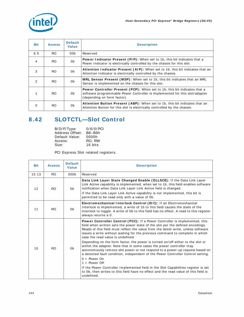
Host-Secondary PCI Express* Bridge Registers (D6:F0)
244 Datasheet
8.42 SLOTCTL—Slot Control
B/D/F/Type: 0/6/0/PCIAddress Offset: B8–B9hDefault Value: 0000hAccess: RO, RW Size: 16 bits
PCI Express Slot related registers.
6:5 RO 00b Reserved
4 RO 0bPower Indicator Present (PIP): When set to 1b, this bit indicates that a Power Indicator is electrically controlled by the chassis for this slot.
3 RO 0bAttention Indicator Present (AIP): When set to 1b, this bit indicates that an Attention Indicator is electrically controlled by the chassis.
2 RO 0bMRL Sensor Present (MSP): When set to 1b, this bit indicates that an MRL Sensor is implemented on the chassis for this slot.
1 RO 0bPower Controller Present (PCP): When set to 1b, this bit indicates that a software programmable Power Controller is implemented for this slot/adapter (depending on form factor).
0 RO 0bAttention Button Present (ABP): When set to 1b, this bit indicates that an Attention Button for this slot is electrically controlled by the chassis.
Bit AccessDefault Value
Description
Bit AccessDefault Value
Description
15:13 RO 000b Reserved
12 RO 0b
Data Link Layer State Changed Enable (DLLSCE): If the Data Link Layer Link Active capability is implemented, when set to 1b, this field enables software notification when Data Link Layer Link Active field is changed.If the Data Link Layer Link Active capability is not implemented, this bit is permitted to be read-only with a value of 0b.
11 RO 0b
Electromechanical Interlock Control (EIC): If an Electromechanical Interlock is implemented, a write of 1b to this field causes the state of the interlock to toggle. A write of 0b to this field has no effect. A read to this register always returns a 0.
10 RO 0b
Power Controller Control (PCC): If a Power Controller is implemented, this field when written sets the power state of the slot per the defined encodings. Reads of this field must reflect the value from the latest write, unless software issues a write without waiting for the previous command to complete in which case the read value is undefined.Depending on the form factor, the power is turned on/off either to the slot or within the adapter. Note that in some cases the power controller may autonomously remove slot power or not respond to a power-up request based on a detected fault condition, independent of the Power Controller Control setting.0 = Power On1 = Power OffIf the Power Controller Implemented field in the Slot Capabilities register is set to 0b, then writes to this field have no effect and the read value of this field is undefined.

Datasheet 245
Host-Secondary PCI Express* Bridge Registers (D6:F0)
9:8 RO 00b
Power Indicator Control (PIC): If a Power Indicator is implemented, writes to this field set the Power Indicator to the written state. Reads of this field must reflect the value from the latest write, unless software issues a write without waiting for the previous command to complete in which case the read value is undefined.00 = Reserved 01 = On 10 = Blink 11 = OffIf the Power Indicator Present bit in the Slot Capabilities register is 0b, this field is permitted to be read-only with a value of 00b.
7:6 RO 00b
Attention Indicator Control (AIC): If an Attention Indicator is implemented, writes to this field set the Attention Indicator to the written state.Reads of this field must reflect the value from the latest write, unless software issues a write without waiting for the previous command to complete in which case the read value is undefined. If the indicator is electrically controlled by chassis, the indicator is controlled directly by the downstream port through implementation specific mechanisms.00 = Reserved 01 = On 10 = Blink 11 = OffIf the Attention Indicator Present bit in the Slot Capabilities register is 0b, this field is permitted to be read only with a value of 00b.
5:4 RO 00b Reserved
3 RW 0bPresence Detect Changed Enable (PDCE): When set to 1b, this bit enables software notification on a presence detect changed event.
2 RO 0b
MRL Sensor Changed Enable (MSCE): When set to 1b, this bit enables software notification on a MRL sensor changed event.Default value of this field is 0b. If the MRL Sensor Present field in the Slot Capabilities register is set to 0b, this bit is permitted to be read-only with a value of 0b.
1 RO 0b
Power Fault Detected Enable (PFDE): When set to 1b, this bit enables software notification on a power fault event.Default value of this field is 0b. If Power Fault detection is not supported, this bit is permitted to be read-only with a value of 0b
0 RO 0bButton Pressed Enable (ABPE): When set to 1b, this bit enables software notification on an attention button pressed event.
Bit AccessDefault Value
Description

Host-Secondary PCI Express* Bridge Registers (D6:F0)
246 Datasheet
8.43 SLOTSTS—Slot Status
B/D/F/Type: 0/6/0/PCIAddress Offset: BA–BBhDefault Value: 0000hAccess: RO, RWC Size: 16 bits
PCI Express Slot related registers.
Bit AccessDefault Value
Description
15:7 RO 0000000b Reserved
6 RO 0b
Presence Detect State (PDS): This bit indicates the presence of an adapter in the slot, reflected by the logical "OR" of the Physical Layer in-band presence detect mechanism and, if present, any out-of-band presence detect mechanism defined for the slot's corresponding form factor. Note that the in-band presence detect mechanism requires that power be applied to an adapter for its presence to be detected. 0 = Slot Empty1 = Card Present in SlotThis register must be implemented on all Downstream Ports that implement slots. For Downstream Ports not connected to slots (where the Slot Implemented bit of the PCI Express Capabilities Register is 0b), this bit must return 1b.
5:4 RO 00b Reserved
3 RWC 0bDetect Changed (PDC): This bit is set when the value reported in Presence Detect State is changed.
2 RO 0bMRL Sensor Changed (MSC): If an MRL sensor is implemented, this bit is set when a MRL Sensor state change is detected. If an MRL sensor is not implemented, this bit must not be set.
1 RO 0b
Power Fault Detected (PFD): If a Power Controller that supports power fault detection is implemented, this bit is set when the Power Controller detects a power fault at this slot. Note that, depending on hardware capability, it is possible that a power fault can be detected at any time, independent of the Power Controller Control setting or the occupancy of the slot. If power fault detection is not supported, this bit must not be set.
0 RO 0bAttention Button Pressed (ABP): If an Attention Button is implemented, this bit is set when the attention button is pressed. If an Attention Button is not supported, this bit must not be set.

Datasheet 247
Host-Secondary PCI Express* Bridge Registers (D6:F0)
8.44 RCTL—Root Control
B/D/F/Type: 0/6/0/PCIAddress Offset: BC–BDhDefault Value: 0000hAccess: RO, RW Size: 16 bits
This register allows control of PCI Express Root Complex specific parameters. The system error control bits in this register determine if corresponding SERRs are generated when our device detects an error (reported in this device's Device Status register) or when an error message is received across the link. Reporting of SERR as controlled by these bits takes precedence over the SERR Enable in the PCI Command Register.
Bit AccessDefault Value
Description
15:4 RO 000h Reserved
3 RW 0b
PME Interrupt Enable (PMEIE): 0 = No interrupts are generated as a result of receiving PME messages.1 = Enables interrupt generation upon receipt of a PME message as reflected in
the PME Status bit of the Root Status Register. A PME interrupt is also generated if the PME Status bit of the Root Status Register is set when this bit is set from a cleared state.
2 RW 0b
System Error on Fatal Error Enable (SEFEE): Controls the Root Complex's response to fatal errors.0 = No SERR generated on receipt of fatal error.1 = Indicates that an SERR should be generated if a fatal error is reported by
any of the devices in the hierarchy associated with this Root Port, or by the Root Port itself.
1 RW 0b
System Error on Non-Fatal Uncorrectable Error Enable (SENFUEE): Controls the Root Complex's response to non-fatal errors.0 = No SERR generated on receipt of non-fatal error.1 = Indicates that an SERR should be generated if a non-fatal error is reported
by any of the devices in the hierarchy associated with this Root Port, or by the Root Port itself.
0 RW 0b
System Error on Correctable Error Enable (SECEE): Controls the Root Complex's response to correctable errors.0 = No SERR generated on receipt of correctable error.1 = Indicates that an SERR should be generated if a correctable error is reported
by any of the devices in the hierarchy associated with this Root Port, or by the Root Port itself.

Host-Secondary PCI Express* Bridge Registers (D6:F0)
248 Datasheet
8.45 RSTS—Root Status
B/D/F/Type: 0/6/0/PCIAddress Offset: C0–C3hDefault Value: 00000000hAccess: RO, RWC Size: 32 bits
This register provides information about PCI Express Root Complex specific parameters.
8.46 PELC—PCI Express Legacy Control
B/D/F/Type: 0/6/0/PCIAddress Offset: EC–EFhDefault Value: 00000000hAccess: RO, RW Size: 32 bits
This register controls functionality that is needed by Legacy (non-PCI Express aware) OSs during run time.
Bit AccessDefault Value
Description
31:18 RO 0000h Reserved
17 RO 0b
PME Pending (PMEP): Indicates that another PME is pending when the PME Status bit is set. When the PME Status bit is cleared by software; the PME is delivered by hardware by setting the PME Status bit again and updating the Requestor ID appropriately. The PME pending bit is cleared by hardware if no more PMEs are pending.
16 RWC 0bPME Status (PMES): Indicates that PME was asserted by the requestor ID indicated in the PME Requestor ID field. Subsequent PMEs are kept pending until the status register is cleared by writing a 1 to this field.
15:0 RO 0000hPME Requestor ID (PMERID): Indicates the PCI requestor ID of the last PME requestor.
Bit AccessDefault Value
Description
31:3 RO0000000
0hReserved
2 RW 0b
PME GPE Enable (PMEGPE): 0 = Do not generate GPE PME message when PME is received.1 = Generate a GPE PME message when PME is received (Assert_PMEGPE and
Deassert_PMEGPE messages on DMI). This enables the MCH to support PMEs on the PCI Express port under legacy OSs.
1 RO 0b Reserved
0 RW 0b
General Message GPE Enable (GENGPE): 0 = Do not forward received GPE assert/de-assert messages.1 = Forward received GPE assert/de-assert messages. These general GPE
message can be received via the PCI Express port from an external Intel device and will be subsequently forwarded to the ICH (via Assert_GPE and Deassert_GPE messages on DMI).

Datasheet 249
Host-Secondary PCI Express* Bridge Registers (D6:F0)
8.47 VCECH—Virtual Channel Enhanced Capability Header
B/D/F/Type: 0/6/0/MMRAddress Offset: 100–103hDefault Value: 14010002hAccess: RO Size: 32 bits
This register indicates PCI Express device Virtual Channel capabilities. Extended capability structures for PCI Express devices are located in PCI Express extended configuration space and have different field definitions than standard PCI capability structures.
8.48 PVCCAP1—Port VC Capability Register 1
B/D/F/Type: 0/6/0/MMRAddress Offset: 104–107hDefault Value: 00000000hAccess: RO Size: 32 bits
This register describes the configuration of PCI Express Virtual Channels associated with this port.
Bit AccessDefault Value
Description
31:20 RO 140hPointer to Next Capability (PNC): The Link Declaration Capability is the next in the PCI Express extended capabilities list.
19:16 RO 1hPCI Express Virtual Channel Capability Version (PCIEVCCV): Hardwired to 1 to indicate compliances with the 1.1 version of the PCI Express specification.Note: This version does not change for 2.0 compliance.
15:0 RO 0002hExtended Capability ID (ECID): Value of 0002h identifies this linked list item (capability structure) as being for PCI Express Virtual Channel registers.
Bit AccessDefault Value
Description
31:7 RO 00000h Reserved
6:4 RO 000b
Low Priority Extended VC Count (LPEVCC): This field indicates the number of (extended) Virtual Channels in addition to the default VC belonging to the low-priority VC (LPVC) group that has the lowest priority with respect to other VC resources in a strict-priority VC Arbitration.The value of 0 in this field implies strict VC arbitration.
3 RO 0b Reserved
2:0 RO 000bExtended VC Count (EVCC): This field indicates the number of (extended) Virtual Channels in addition to the default VC supported by the device.
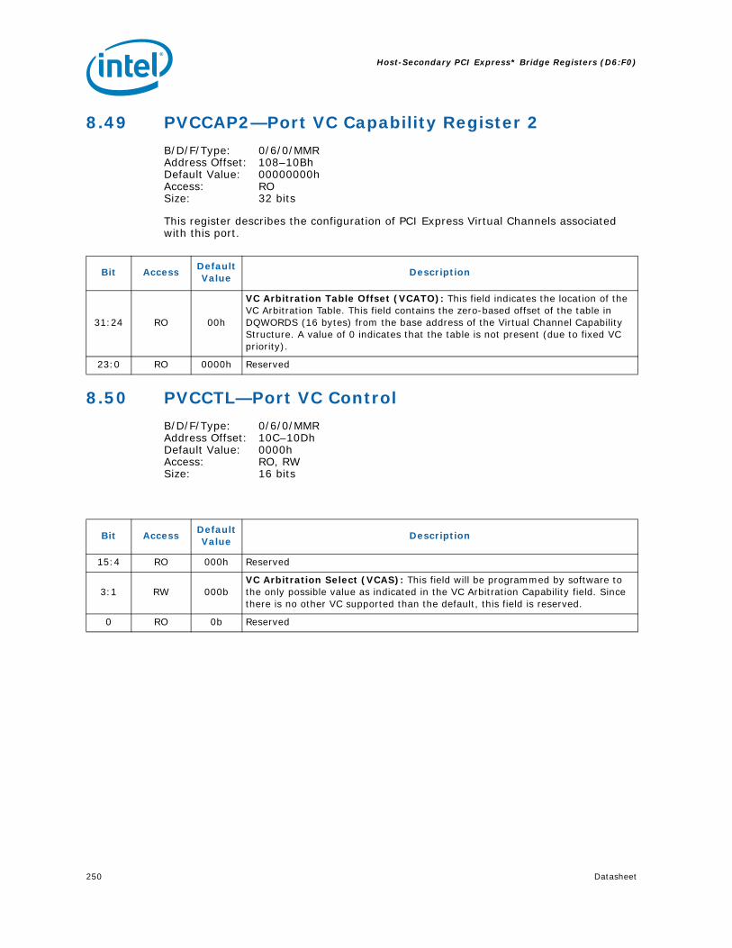
Host-Secondary PCI Express* Bridge Registers (D6:F0)
250 Datasheet
8.49 PVCCAP2—Port VC Capability Register 2
B/D/F/Type: 0/6/0/MMRAddress Offset: 108–10BhDefault Value: 00000000hAccess: RO Size: 32 bits
This register describes the configuration of PCI Express Virtual Channels associated with this port.
8.50 PVCCTL—Port VC Control
B/D/F/Type: 0/6/0/MMRAddress Offset: 10C–10DhDefault Value: 0000hAccess: RO, RW Size: 16 bits
Bit AccessDefault Value
Description
31:24 RO 00h
VC Arbitration Table Offset (VCATO): This field indicates the location of the VC Arbitration Table. This field contains the zero-based offset of the table in DQWORDS (16 bytes) from the base address of the Virtual Channel Capability Structure. A value of 0 indicates that the table is not present (due to fixed VC priority).
23:0 RO 0000h Reserved
Bit AccessDefault Value
Description
15:4 RO 000h Reserved
3:1 RW 000bVC Arbitration Select (VCAS): This field will be programmed by software to the only possible value as indicated in the VC Arbitration Capability field. Since there is no other VC supported than the default, this field is reserved.
0 RO 0b Reserved

Datasheet 251
Host-Secondary PCI Express* Bridge Registers (D6:F0)
8.51 VC0RCAP—VC0 Resource Capability
B/D/F/Type: 0/6/0/MMRAddress Offset: 110–113hDefault Value: 00000001hAccess: RO Size: 32 bits
Bit AccessDefault Value
Description
31:16 RO 0000h Reserved
15 RO 0b
Reject Snoop Transactions (RSNPT): 0 = Transactions with or without the No Snoop bit set within the Transaction
Layer Packet header are allowed on this VC.1 = When Set, any transaction for which the No Snoop attribute is applicable but
is not Set within the TLP Header will be rejected as an Unsupported Request.
14:8 RO 0000h Reserved
7:0 RO 01h
Port Arbitration Capability: Indicates types of Port Arbitrationsupported by the VC resource. This field is valid for all Switch Ports, Root Ports that support peer-to-peer traffic, and RCRBs, but not for PCI Express Endpoint devices or Root Ports that do not support peer to peer traffic.Each bit location within this field corresponds to a Port Arbitration Capability defined below. When more than one bit in this field is Set, it indicates that the VC resource can be configured to provide different arbitration services.Software selects among these capabilities by writing to the Port Arbitration Select field (see below).Bit[0] = Default = 01b; Non-configurable hardware-fixed arbitration
scheme, e.g., Round Robin (RR)Bit[1] = Weighted Round Robin (WRR) arbitration with 32 phasesBit[2] = WRR arbitration with 64 phasesBit[3] = WRR arbitration with 128 phasesBit[4] = Time-based WRR with 128 phasesBit[5] = WRR arbitration with 256 phasesBits[6:7] = ReservedMCH default indicates "Non-configurable hardware-fixed arbitration scheme".

Host-Secondary PCI Express* Bridge Registers (D6:F0)
252 Datasheet
8.52 VC0RCTL—VC0 Resource Control
B/D/F/Type: 0/6/0/MMRAddress Offset: 114–117hDefault Value: 800000FFhAccess: RO, RW Size: 32 bits
This register controls the resources associated with PCI Express Virtual Channel 0.
Bit AccessDefault Value
Description
31 RO 1bVC0 Enable (VC0E): For VC0, this is hardwired to 1 and read only as VC0 can never be disabled.
30:27 RO 0h Reserved
26:24 RO 000bVC0 ID (VC0ID): This field assigns a VC ID to the VC resource. For VC0 this is hardwired to 0 and read only.
23:20 RO 0000h Reserved
19:17 RW 000b
Port Arbitration Select: This field configures the VC resource to provide a particular Port Arbitration service. This field is valid for RCRBs, Root Ports that support peer to peer traffic, and Switch Ports, but not for PCI Express Endpoint devices or Root Ports that do not support peer to peer traffic.The permissible value of this field is a number corresponding to one of the asserted bits in the Port Arbitration Capability field of the VC resource.
16:8 RO 00h Reserved
7:1 RW 7Fh
TC/VC0 Map (TCVC0M): This field indicates the TCs (Traffic Classes) that are mapped to the VC resource. Bit locations within this field correspond to TC values. For example, when bit 7 is set in this field, TC7 is mapped to this VC resource. When more than one bit in this field is set, it indicates that multiple TCs are mapped to the VC resource. To remove one or more TCs from the TC/VC Map of an enabled VC, software must ensure that no new or outstanding transactions with the TC labels are targeted at the given Link.
0 RO 1b TC0/VC0 Map (TC0VC0M): Traffic Class 0 is always routed to VC0.

Datasheet 253
Host-Secondary PCI Express* Bridge Registers (D6:F0)
8.53 VC0RSTS—VC0 Resource Status
B/D/F/Type: 0/6/0/MMRAddress Offset: 11A–11BhDefault Value: 0002hAccess: RO Size: 16 bits
This register reports the Virtual Channel specific status.
8.54 RCLDECH—Root Complex Link Declaration Enhanced
B/D/F/Type: 0/6/0/MMRAddress Offset: 140–143hDefault Value: 00010005hAccess: RO Size: 32 bits
This capability declares links from this element (PCI Express) to other elements of the root complex component to which it belongs. See PCI Express specification for link/topology declaration requirements.
Bit AccessDefault Value
Description
15:2 RO 0000h Reserved
1 RO 1b
VC0 Negotiation Pending (VC0NP): 0 = The VC negotiation is complete.1 = The VC resource is still in the process of negotiation (initialization or
disabling).This bit indicates the status of the process of Flow Control initialization. It is set by default on Reset, as well as whenever the corresponding Virtual Channel is Disabled or the Link is in the DL_Down state. It is cleared when the link successfully exits the FC_INIT2 state.Before using a Virtual Channel, software must check whether the VC Negotiation Pending fields for that Virtual Channel are cleared in both Components on a Link.
0 RO 0b Reserved
Bit AccessDefault Value
Description
31:20 RO 000hPointer to Next Capability (PNC): This is the last capability in the PCI Express extended capabilities list.
19:16 RO 1hLink Declaration Capability Version (LDCV): Hardwired to 1 to indicate compliances with the 1.1 version of the PCI Express specification.Note: This version does not change for 2.0 compliance.
15:0 RO 0005hExtended Capability ID (ECID): Value of 0005h identifies this linked list item (capability structure) as being for PCI Express Link Declaration Capability.

Host-Secondary PCI Express* Bridge Registers (D6:F0)
254 Datasheet
8.55 ESD—Element Self Description
B/D/F/Type: 0/6/0/MMRAddress Offset: 144–147hDefault Value: 03000100hAccess: RO, RWO Size: 32 bits
This register provides information about the root complex element containing this Link Declaration Capability.
Bit AccessDefault Value
Description
31:24 RO 03h
Port Number (PN): This field specifies the port number associated with this element with respect to the component that contains this element. This port number value is used by the egress port of the component to provide arbitration to this Root Complex Element.
23:16 RWO 00hComponent ID (CID): This field indicates the physical component that contains this Root Complex Element.
15:8 RO 01hNumber of Link Entries (NLE): This field indicates the number of link entries following the Element Self Description. This field reports 1 (to Egress port only as we don't report any peer-to-peer capabilities in our topology).
7:4 RO 0h Reserved
3:0 RO 0h Element Type (ET): This field indicates Configuration Space Element.

Datasheet 255
Host-Secondary PCI Express* Bridge Registers (D6:F0)
8.56 LE1D—Link Entry 1 Description
B/D/F/Type: 0/6/0/MMRAddress Offset: 150–153hDefault Value: 00000000hAccess: RO, RWO Size: 32 bits
This register provides the first part of a Link Entry that declares an internal link to another Root Complex Element.
8.57 LE1A—Link Entry 1 Address
B/D/F/Type: 0/6/0/MMRAddress Offset: 158–15FhDefault Value: 0000000000000000hAccess: RO, RWO Size: 64 bits
This register provides the second part of a Link Entry that declares an internal link to another Root Complex Element.
§ §
Bit AccessDefault Value
Description
31:24 RO 00h
Target Port Number (TPN): This field specifies the port number associated with the element targeted by this link entry (Egress Port). The target port number is with respect to the component that contains this element as specified by the target component ID.
23:16 RWO 00hTarget Component ID (TCID): This field identifies the physical or logical component that is targeted by this link entry.
15:2 RO 0000h Reserved
1 RO 0bLink Type (LTYP): This bit indicates that the link points to memory–mapped space (for RCRB). The link address specifies the 64-bit base address of the target RCRB.
0 RWO 0bLink Valid (LV): 0 = Link Entry is not valid and will be ignored.1 = Link Entry specifies a valid link.
Bit AccessDefault Value
Description
63:32 RO0000000
0hReserved
31:12 RWO 00000hLink Address (LA): This field provides the memory mapped base address of the RCRB that is the target element (Egress Port) for this link entry.
11:0 RO 000h Reserved

Host-Secondary PCI Express* Bridge Registers (D6:F0)
256 Datasheet

Datasheet 257
Direct Media Interface (DMI) RCRB
9 Direct Media Interface (DMI) RCRB
This Root Complex Register Block (RCRB) controls the MCH-ICH9 serial interconnect. The base address of this space is programmed in DMIBAR in D0:F0 configuration space. Table 16 provides an address map of the DMI registers listed by address offset in ascending order.
Note: IMPORTANT: All RCRB register space needs to remain organized as shown here.
Table 16. Direct Media Interface Register Address Map
Address Offset
Register Symbol
Register NameDefault Value
Access
0–3h DMIVCECHDMI Virtual Channel Enhanced Capability
04010002h RO
4–7h DMIPVCCAP1 DMI Port VC Capability Register 1 00000001h RWO, RO
C–Dh DMIPVCCTL DMI Port VC Control 0000h RO, RW
10–13h DMIVC0RCAP DMI VC0 Resource Capability 00000001h RO
14–17h DMIVC0RCTL0 DMI VC0 Resource Control 800000FFh RO, RW
1A–1Bh DMIVC0RSTS DMI VC0 Resource Status 0002h RO
1C–1Fh DMIVC1RCAP DMI VC1 Resource Capability 00008001h RO
20–23h DMIVC1RCTL1 DMI VC1 Resource Control 01000000h RW, RO
26–27h DMIVC1RSTS DMI VC1 Resource Status 0002h RO
84–87h DMILCAP DMI Link Capabilities 00012C41h RO, RWO
88–89h DMILCTL DMI Link Control 0000h RW, RO
8A–8Bh DMILSTS DMI Link Status 0001h RO
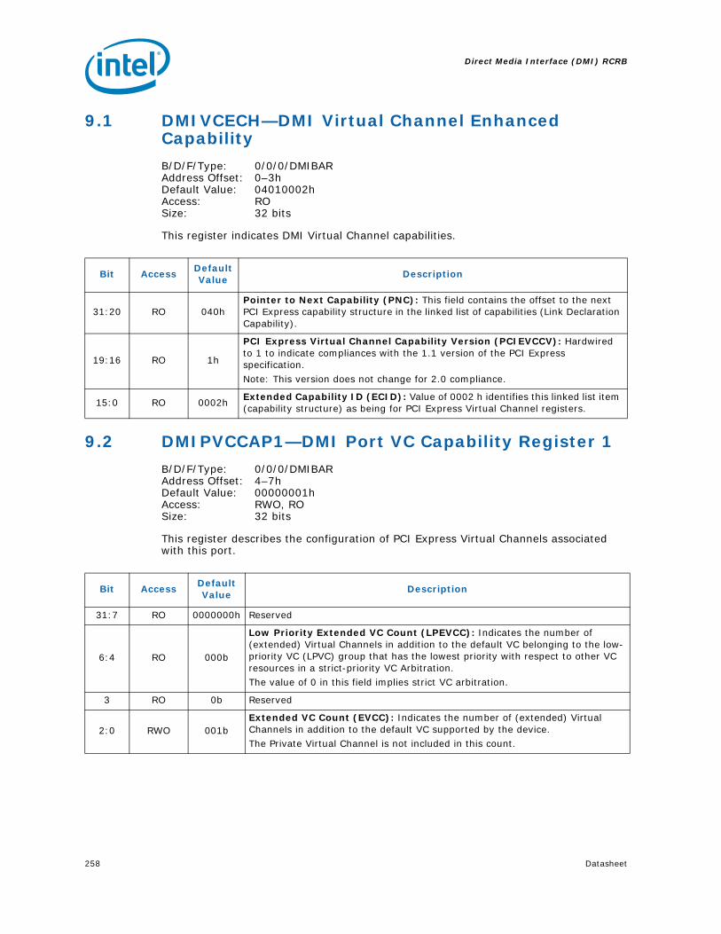
Direct Media Interface (DMI) RCRB
258 Datasheet
9.1 DMIVCECH—DMI Virtual Channel Enhanced Capability
B/D/F/Type: 0/0/0/DMIBARAddress Offset: 0–3hDefault Value: 04010002hAccess: ROSize: 32 bits
This register indicates DMI Virtual Channel capabilities.
9.2 DMIPVCCAP1—DMI Port VC Capability Register 1
B/D/F/Type: 0/0/0/DMIBARAddress Offset: 4–7hDefault Value: 00000001hAccess: RWO, RO Size: 32 bits
This register describes the configuration of PCI Express Virtual Channels associated with this port.
Bit AccessDefault Value
Description
31:20 RO 040hPointer to Next Capability (PNC): This field contains the offset to the next PCI Express capability structure in the linked list of capabilities (Link Declaration Capability).
19:16 RO 1h
PCI Express Virtual Channel Capability Version (PCIEVCCV): Hardwired to 1 to indicate compliances with the 1.1 version of the PCI Express specification.
Note: This version does not change for 2.0 compliance.
15:0 RO 0002hExtended Capability ID (ECID): Value of 0002 h identifies this linked list item (capability structure) as being for PCI Express Virtual Channel registers.
Bit AccessDefault Value
Description
31:7 RO 0000000h Reserved
6:4 RO 000b
Low Priority Extended VC Count (LPEVCC): Indicates the number of (extended) Virtual Channels in addition to the default VC belonging to the low-priority VC (LPVC) group that has the lowest priority with respect to other VC resources in a strict-priority VC Arbitration.The value of 0 in this field implies strict VC arbitration.
3 RO 0b Reserved
2:0 RWO 001bExtended VC Count (EVCC): Indicates the number of (extended) Virtual Channels in addition to the default VC supported by the device.The Private Virtual Channel is not included in this count.
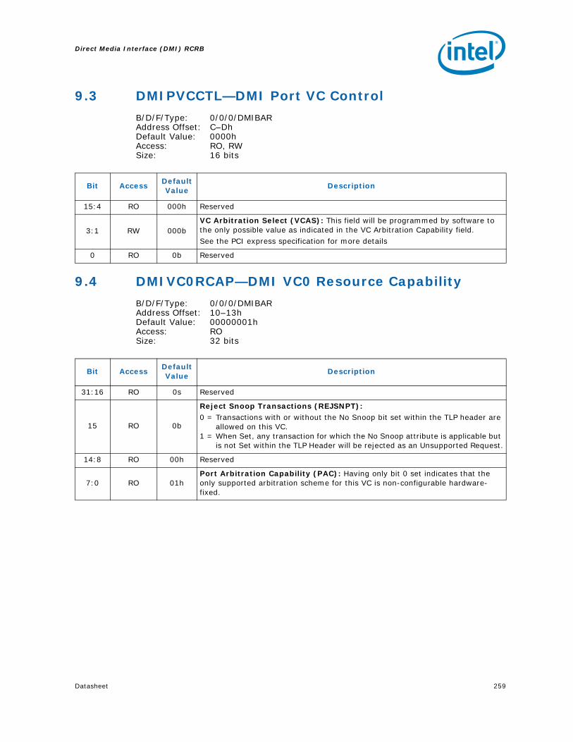
Datasheet 259
Direct Media Interface (DMI) RCRB
9.3 DMIPVCCTL—DMI Port VC Control
B/D/F/Type: 0/0/0/DMIBARAddress Offset: C–DhDefault Value: 0000hAccess: RO, RW Size: 16 bits
9.4 DMIVC0RCAP—DMI VC0 Resource Capability
B/D/F/Type: 0/0/0/DMIBARAddress Offset: 10–13hDefault Value: 00000001hAccess: ROSize: 32 bits
Bit AccessDefault Value
Description
15:4 RO 000h Reserved
3:1 RW 000bVC Arbitration Select (VCAS): This field will be programmed by software to the only possible value as indicated in the VC Arbitration Capability field.See the PCI express specification for more details
0 RO 0b Reserved
Bit AccessDefault Value
Description
31:16 RO 0s Reserved
15 RO 0b
Reject Snoop Transactions (REJSNPT): 0 = Transactions with or without the No Snoop bit set within the TLP header are
allowed on this VC.1 = When Set, any transaction for which the No Snoop attribute is applicable but
is not Set within the TLP Header will be rejected as an Unsupported Request.
14:8 RO 00h Reserved
7:0 RO 01hPort Arbitration Capability (PAC): Having only bit 0 set indicates that the only supported arbitration scheme for this VC is non-configurable hardware-fixed.

Direct Media Interface (DMI) RCRB
260 Datasheet
9.5 DMIVC0RCTL0—DMI VC0 Resource Control
B/D/F/Type: 0/0/0/DMIBARAddress Offset: 14–17hDefault Value: 800000FFhAccess: RO, RW Size: 32 bits
This register controls the resources associated with PCI Express Virtual Channel 0.
Bit AccessDefault Value
Description
31 RO 1bVirtual Channel 0 Enable (VC0E): For VC0 this is hardwired to 1 and read only as VC0 can never be disabled.
30:27 RO 0h Reserved
26:24 RO 000bVirtual Channel 0 ID (VC0ID): Assigns a VC ID to the VC resource. For VC0 this is hardwired to 0 and read only.
23:20 RO 0h Reserved
19:17 RW 000b
Port Arbitration Select (PAS): This field configures the VC resource to provide a particular Port Arbitration service. Valid value for this field is a number corresponding to one of the asserted bits in the Port Arbitration Capability field of the VC resource. Because only bit 0 of that field is asserted.This field will always be programmed to 1.
16:8 RO 000h Reserved
7:1 RW 7Fh
Traffic Class / Virtual Channel 0 Map (TCVC0M): This field indicates the TCs (Traffic Classes) that are mapped to the VC resource. Bit locations within this field correspond to TC values.For example, when bit 7 is set in this field, TC7 is mapped to this VC resource. When more than one bit in this field is set, it indicates that multiple TCs are mapped to the VC resource. In order to remove one or more TCs from the TC/VC Map of an enabled VC, software must ensure that no new or outstanding transactions with the TC labels are targeted at the given Link.
0 RO 1bTraffic Class 0 / Virtual Channel 0 Map (TC0VC0M): Traffic Class 0 is always routed to VC0.

Datasheet 261
Direct Media Interface (DMI) RCRB
9.6 DMIVC0RSTS—DMI VC0 Resource Status
B/D/F/Type: 0/0/0/DMIBARAddress Offset: 1A–1BhDefault Value: 0002hAccess: RO Size: 16 bits
This register reports the Virtual Channel specific status.
9.7 DMIVC1RCAP—DMI VC1 Resource Capability
B/D/F/Type: 0/0/0/DMIBARAddress Offset: 1C–1FhDefault Value: 00008001hAccess: RO Size: 32 bits
Bit AccessDefault Value
Description
15:2 RO 0000h Reserved
1 RO 1b
Virtual Channel 0 Negotiation Pending (VC0NP): 0 = The VC negotiation is complete.1 = The VC resource is still in the process of negotiation (initialization or
disabling).This bit indicates the status of the process of Flow Control initialization. It is set by default on Reset, as well as whenever the corresponding Virtual Channel is Disabled or the Link is in the DL_Down state.
It is cleared when the link successfully exits the FC_INIT2 state.BIOS Requirement: Before using a Virtual Channel, software must check whether the VC Negotiation Pending fields for that Virtual Channel are cleared in both Components on a Link.
0 RO 0b Reserved
Bit AccessDefault Value
Description
31:16 RO 00h Reserved
15 RO 1b
Reject Snoop Transactions (REJSNPT): 0 = Transactions with or without the No Snoop bit set within the TLP header are
allowed on this VC.1 = When Set, any transaction for which the No Snoop attribute is applicable but
is not Set within the TLP Header will be rejected as an Unsupported Request.
14:8 RO 00h Reserved
7:0 RO 01hPort Arbitration Capability (PAC): Having only bit 0 set indicates that the only supported arbitration scheme for this VC is non-configurable hardware-fixed.

Direct Media Interface (DMI) RCRB
262 Datasheet
9.8 DMIVC1RCTL1—DMI VC1 Resource Control
B/D/F/Type: 0/0/0/DMIBARAddress Offset: 20–23hDefault Value: 01000000hAccess: RW, RO Size: 32 bits
This register controls the resources associated with PCI Express Virtual Channel 1.
Bit AccessDefault Value
Description
31 RW 0bVirtual Channel 1 Enable (VC1E): 0 = Virtual Channel is disabled.1 = Virtual Channel is enabled.
30:27 RO 0h Reserved
26:24 RW 001bVirtual Channel 1 ID (VC1ID): This field assigns a VC ID to the VC resource. Assigned value must be non-zero. This field can not be modified when the VC is already enabled.
23:20 RO 0h Reserved
19:17 RW 000b
Port Arbitration Select (PAS): This field configures the VC resource to provide a particular Port Arbitration service. Valid value for this field is a number corresponding to one of the asserted bits in the Port Arbitration Capability field of the VC resource.
16:8 RO 000h Reserved
7:1 RW 00h
Traffic Class / Virtual Channel 1 Map (TCVC1M): This field indicates the TCs (Traffic Classes) that are mapped to the VC resource. Bit locations within this field correspond to TC values.For example, when bit 7 is set in this field, TC7 is mapped to this VC resource. When more than one bit in this field is set, it indicates that multiple TCs are mapped to the VC resource. To remove one or more TCs from the TC/VC Map of an enabled VC, software must ensure that no new or outstanding transactions with the TC labels are targeted at the given Link.
0 RO 0bTraffic Class 0 / Virtual Channel 1 Map (TC0VC1M): Traffic Class 0 is always routed to VC0.
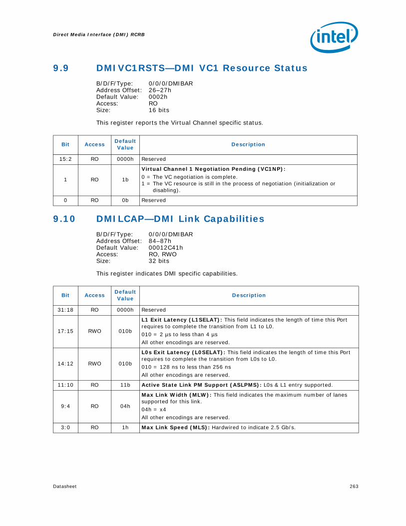
Datasheet 263
Direct Media Interface (DMI) RCRB
9.9 DMIVC1RSTS—DMI VC1 Resource Status
B/D/F/Type: 0/0/0/DMIBARAddress Offset: 26–27hDefault Value: 0002hAccess: RO Size: 16 bits
This register reports the Virtual Channel specific status.
9.10 DMILCAP—DMI Link Capabilities
B/D/F/Type: 0/0/0/DMIBARAddress Offset: 84–87hDefault Value: 00012C41hAccess: RO, RWO Size: 32 bits
This register indicates DMI specific capabilities.
Bit AccessDefault Value
Description
15:2 RO 0000h Reserved
1 RO 1b
Virtual Channel 1 Negotiation Pending (VC1NP): 0 = The VC negotiation is complete.1 = The VC resource is still in the process of negotiation (initialization or
disabling).
0 RO 0b Reserved
Bit AccessDefault Value
Description
31:18 RO 0000h Reserved
17:15 RWO 010b
L1 Exit Latency (L1SELAT): This field indicates the length of time this Port requires to complete the transition from L1 to L0. 010 = 2 µs to less than 4 µsAll other encodings are reserved.
14:12 RWO 010b
L0s Exit Latency (L0SELAT): This field indicates the length of time this Port requires to complete the transition from L0s to L0. 010 = 128 ns to less than 256 nsAll other encodings are reserved.
11:10 RO 11b Active State Link PM Support (ASLPMS): L0s & L1 entry supported.
9:4 RO 04h
Max Link Width (MLW): This field indicates the maximum number of lanes supported for this link.04h = x4All other encodings are reserved.
3:0 RO 1h Max Link Speed (MLS): Hardwired to indicate 2.5 Gb/s.

Direct Media Interface (DMI) RCRB
264 Datasheet
9.11 DMILCTL—DMI Link Control
B/D/F/Type: 0/0/0/DMIBARAddress Offset: 88–89hDefault Value: 0000hAccess: RW, RO Size: 16 bits
This register allows control of DMI.
9.12 DMILSTS—DMI Link Status
B/D/F/Type: 0/0/0/DMIBARAddress Offset: 8A–8BhDefault Value: 0001hAccess: RO Size: 16 bits
This register indicates DMI status.
§ §
Bit AccessDefault Value
Description
15:8 RO 00h Reserved
7 RW 0b
Extended Synch (EXTSYNC): 0 = Standard Fast Training Sequence (FTS).1 = Forces the transmission of additional ordered sets when exiting the L0s
state and when in the Recovery state.
6:3 RO 0h Reserved
2 RW 0b Far-End Digital Loopback (FEDLB):
1:0 RW 00b
Active State Power Management Support (ASPMS): This field controls the level of active state power management supported on the given link.00 = Disabled01 = L0s Entry Supported10 = Reserved11 = L0s and L1 Entry Supported
Bit AccessDefault Value
Description
15:4 RO 0s Reserved
3:0 RO 1hNegotiated Speed (NSPD): This field indicates negotiated link speed.1h = 2.5 Gb/sAll other encodings are reserved.
Datasheet 265
Functional Description
10 Functional Description
10.1 Host Interface
The MCH supports Intel® CoreTM2 Duo and Intel® Core™2 Quad processors. The cache line size is 64 bytes. Source synchronous transfer is used for the address and data signals. The address signals are double pumped and a new address can be generated every other bus clock. At 200/267/333MHz bus clock the address signals run at 667MT/s. The data is quad pumped and an entire 64B cache line can be transferred in two bus clocks. At 200/266/333MHz bus clock, the data signals run at 800/1066/1333MT/s for a maximum bandwidth of 6.4/8.5/10.6GB/s.
10.1.1 FSB IOQ Depth
The Scalable Bus supports up to 12 simultaneous outstanding transactions.
10.1.2 FSB OOQ Depth
The MCH supports only one outstanding deferred transaction on the FSB.
10.1.3 FSB GTL+ Termination
The MCH integrates GTL+ termination resistors on die.
10.1.4 FSB Dynamic Bus Inversion
The MCH supports Dynamic Bus Inversion (DBI) when driving and when receiving data from the processor. DBI limits the number of data signals that are driven to a low voltage on each quad pumped data phase. This decreases the worst-case power consumption of the MCH. HDINV[3:0]# indicate if the corresponding 16 bits of data are inverted on the bus for each quad pumped data phase:
When the processor or the MCH drives data, each 16-bit segment is analyzed. If more than 8 of the 16 signals would normally be driven low on the bus, the corresponding HDINV# signal will be asserted, and the data will be inverted prior to being driven on the bus. When the processor or the MCH receives data, it monitors HDINV#[3:0] to determine if the corresponding data segment should be inverted.
HDINV#[3:0] Data Bits
HDINV0# HD[15:0]#
HDINV1# HD[31:16]#
HDINV2# HD[47:32]#
HDINV3# HD[63:48]#

Functional Description
266 Datasheet
10.1.5 APIC Cluster Mode Support
APIC Cluster mode support is required for backwards compatibility with existing software, including various operating systems.
The MCH supports three types of interrupt re-direction:
• Physical
• Flat-Logical
• Clustered-Logical
Table 17. Host Interface 4X, 2X, and 1X Signal Groups
Signals Associated Clock or Strobe Signal Group
ADS#, BNR#, BPRI#, DEFER#, DBSY#, DRDY#, HIT#, HITM#, LOCK#, RS[2:0]#, TRDY#, RESET, BR0#
BCLK
1X
HA[16:3]#, REQ[4:0]# ADSTB[0]#2X
HA[35:17]# ADSTB[1]#
D[15:0]#, DBI0# DSTBP0#, DSTBN0#
4XD[31:16]#, DBI1# DSTBP1#, DSTBN1#
D[47:32]#, DBI2# DSTBP2#, DSTBN2#
D[63:48]#, DBI3# DSTBP3#, DSTBN3#

Datasheet 267
Functional Description
10.2 System Memory Controller
The system memory controller supports both DDR2 and DDR3 protocols with two independent 64 bit wide channels each accessing one or two DIMMs. It supports a maximum of two un-buffered ECC or non-ECC DDR2 DIMMs or two un-buffered non-ECC DDR3 DIMMs per channel thus allowing up to four device ranks per channel.
10.2.1 System Memory Organization Modes
The system memory controller supports two memory organization modes, Single Channel and Dual Channel.
10.2.1.1 Single Channel Mode
In this mode, all memory cycles are directed to a single channel.
Single channel mode is used when either Channel A or Channel B DIMMs are populated in any order, but not both.
10.2.1.2 Dual Channel Modes
10.2.1.2.1 Dual Channel Symmetric Mode
This mode provides maximum performance on real applications. Addresses are ping-ponged between the channels after each cache line (64 byte boundary). If there are two requests, and the second request is to an address on the opposite channel from the first, that request can be sent before data from the first request has returned. If two consecutive cache lines are requested, both may be retrieved simultaneously, since they are guaranteed to be on opposite channels.
Dual channel symmetric mode is used when both Channel A and Channel B DIMMs are populated in any order with the total amount of memory in each channel being the same, but the DRAM device technology and width may vary from one channel to the other.
Table 18 is a sample dual channel symmetric memory configuration showing the rank organization.
Table 18. Sample System Memory Dual Channel Symmetric Organization Mode
RankChannel 0 Population
Cumulative Top Address in Channel 0
Channel 1 Population
Cumulative Top Address in Channel 1
Rank 3 0 MB 2560 MB 0 MB 2560 MB
Rank 2 256 MB 2560 MB 256 MB 2560 MB
Rank 1 512 MB 2048 MB 512 MB 2048 MB
Rank 0 512 MB 1024 MB 512 MB 1024 MB

Functional Description
268 Datasheet
10.2.1.2.2 Dual Channel Asymmetric Mode with Intel® Flex Memory Mode Enabled
In this addressing mode the lowest DRAM memory is mapped to dual channel operation and the top most DRAM memory is mapped to single channel operation. In this mode the system can run at one zone of dual channel mode and one zone of single channel mode simultaneously across the whole memory array.
This mode is used when Intel® Flex Memory Mode is enabled and both Channel A and Channel B DIMMs are populated in any order with the total amount of memory in each channel being different.
Table 19 is a sample dual channel asymmetric memory configuration showing the rank organization with Intel® Flex Memory Mode Enabled.
10.2.1.2.3 Dual Channel Asymmetric Mode with Intel® Flex Memory Mode Disabled
In this addressing mode addresses start in channel 0 and stay there until the end of the highest rank in channel 0, and then addresses continue from the bottom of channel 1 to the top.
This mode is used when Intel® Flex Memory Mode is disabled and both Channel A and Channel B DIMMs are populated in any order with the total amount of memory in each channel being different.
Table 20 is a sample dual channel asymmetric memory configuration showing the rank organization with Intel® Flex Memory Mode Disabled:
Table 19. Sample System Memory Dual Channel Asymmetric Organization Mode with Intel® Flex Memory Mode Enabled
RankChannel 0 population
Cumulative top address in Channel 0
Channel 1 population
Cumulative top address in Channel 1
Rank 3 0 MB 2048 MB 0 MB 2304 MB
Rank 2 0 MB 2048 MB 256 MB 2304 MB
Rank 1 512 MB 2048 MB 512 MB 2048 MB
Rank 0 512 MB 1024 MB 512 MB 1024 MB
Table 20. Sample System Memory Dual Channel Asymmetric Organization Mode with Intel® Flex Memory Mode Disabled
RankChannel 0 population
Cumulative top address in Channel 0
Channel 1 population
Cumulative top address in Channel 1
Rank 3 0 MB 1280 MB 0 MB 2304 MB
Rank 2 256 MB 1280 MB 0 MB 2304 MB
Rank 1 512 MB 1024 MB 512 MB 2304 MB
Rank 0 512 MB 512 MB 512 MB 1792 MB
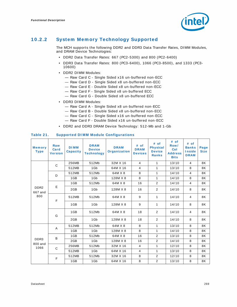
Datasheet 269
Functional Description
10.2.2 System Memory Technology Supported
The MCH supports the following DDR2 and DDR3 Data Transfer Rates, DIMM Modules, and DRAM Device Technologies:
• DDR2 Data Transfer Rates: 667 (PC2-5300) and 800 (PC2-6400)
• DDR3 Data Transfer Rates: 800 (PC3-6400), 1066 (PC3-8500), and 1333 (PC3-10600)
• DDR2 DIMM Modules:— Raw Card C - Single Sided x16 un-buffered non-ECC— Raw Card D - Single Sided x8 un-buffered non-ECC— Raw Card E - Double Sided x8 un-buffered non-ECC— Raw Card F - Single Sided x8 un-buffered ECC— Raw Card G - Double Sided x8 un-buffered ECC
• DDR3 DIMM Modules:— Raw Card A - Single Sided x8 un-buffered non-ECC— Raw Card B - Double Sided x8 un-buffered non-ECC— Raw Card C - Single Sided x16 un-buffered non-ECC— Raw Card F - Double Sided x16 un-buffered non-ECC
• DDR2 and DDR3 DRAM Device Technology: 512-Mb and 1-Gb
Table 21. Supported DIMM Module Configurations
Memory Type
Raw Card
Version
DIMM Capacity
DRAM Device
Technology
DRAM Organization
# of DRAM
Devices
# of Physical Device Ranks
# of Row/
Col Address
Bits
# of Banks Inside DRAM
Page Size
DDR2 667 and
800
C256MB 512Mb 32M X 16 4 1 13/10 4 8K
512MB 1Gb 64M X 16 4 1 13/10 8 8K
D512MB 512Mb 64M X 8 8 1 14/10 4 8K
1GB 1Gb 128M X 8 8 1 14/10 8 8K
E1GB 512Mb 64M X 8 16 2 14/10 4 8K
2GB 1Gb 128M X 8 16 2 14/10 8 8K
F512MB 512Mb 64M X 8 9 1 14/10 4 8K
1GB 1Gb 128M X 8 9 1 14/10 8 8K
G1GB 512Mb 64M X 8 18 2 14/10 4 8K
2GB 1Gb 128M X 8 18 2 14/10 8 8K
DDR3 800 and
1066
A512MB 512Mb 64M X 8 8 1 13/10 8 8K
1GB 1Gb 128M X 8 8 1 14/10 8 8K
B1GB 512Mb 64M X 8 16 2 13/10 8 8K
2GB 1Gb 128M X 8 16 2 14/10 8 8K
C256MB 512Mb 32M X 16 4 1 12/10 8 8K
512MB 1Gb 64M X 16 4 1 13/10 8 8K
F512MB 512Mb 32M X 16 8 2 12/10 8 8K
1GB 1Gb 64M X 16 8 2 13/10 8 8K

Functional Description
270 Datasheet
10.2.3 Error Checking and Correction
Table 22 is used to calculate the syndrome. Numbers in parentheses indicate the data content of that bit position. For example, bit position 36 holds the data originally in data bit 32.
Table 22. Syndrome Bit Values
Syndrome Bit > Data Bit
7 6 5 4 3 2 1 0
0 X X X
1 X X X
2 X X X
3 X X X
4 X X X
5 X X X
6 X X X
7 X X X
8 X X X
9 X X X
10 X X X
11 X X X
12 X X X
13 X X X
14 X X X
15 X X X
16 X X X
17 X X X
18 X X X
19 X X X
20 X X X
21 X X X
22 X X X
23 X X X
24 X X X X X
25 X X X X X
26 (CB2) X
27 (CB5) X
28 (26) X X X
29 (27) X X X
30 (28) X X X
31 (29) X X X
32 (30) X X X X X

Datasheet 271
Functional Description
33 (31) X X X X X
34 (CB3) X
35 (CB4) X
36 (32) X X X
37 (33) X X X
38 (34) X X X
39 (35) X X X
40 (36) X X X
41 (37) X X X
42 (38) X X X
43 (39) X X X
44 (40) X X X
45 (41) X X X
46 (42) X X X
47 (43) X X X
48 (44) X X X
49 (45) X X X
50 (46) X X X
51 (47) X X X
52 (48) X X X
53 (49) X X X
54 (50) X X X
55 (51) X X X
56 (52) X X X
57 (53) X X X
58 (54) X X X
59 (55) X X X
60 (56) X X X X X
61 (57) X X X X X
62 (CB6) X
63 (CB1) X
CB0 (58) X X X
CB1 (59) X X X
CB2 (60) X X X
CB3 (61) X X X
CB4 (62) X X X X X
Table 22. Syndrome Bit Values
Syndrome Bit > Data Bit
7 6 5 4 3 2 1 0

Functional Description
272 Datasheet
Every data bit appears in either exactly 3 or exactly 5 check bit and syndrome bit equations. Every check bit appears en exactly 1 syndrome bit equation. This leads to six cases.
1. If the data comes back exactly as it was written, then the calculated check byte will match the stored check byte, and the syndrome will be all 0s.
2. If exactly one check bit is flipped between the time it is written and the time it is read back, then the syndrome will contain exactly one 1. Since the check byte is not returned to the requesting agent, no action is necessary.
3. If exactly one data bit is flipped between the time it is written and the time it is read back, then the syndrome will contain either exactly three 1s or exactly five 1s. The syndrome can then be decoded as a pointer to the bit that flipped using the same check byte generation table in reverse. If the syndrome contains 1s that match the locations of all three or all five Xs in a given row, then that is the bit which should be flipped before the QWord is returned to the requesting agent.
4. If exactly two bits flipped, there will be a nonzero even number of 1s in the syndrome. It cannot be determined which bits flipped based on that syndrome, but a multi-bit error will be recorded along with the address at which the error occurred. In addition, bits 0 and 31 of each DWord are forced to 0 in the returned data in case this read was a TLB fetch. This ensures that the table entry is invalid, such that additional data corruption can be avoided.
5. If an even number of bits greater than two flipped, there will be an even number of 1s in the syndrome, but that even number could be zero, such that detection of this scenario is not ensured. If the syndrome contains a nonzero number of 1s, it cannot be distinguished from scenario 4 above.
6. It is possible for an odd number of bits greater than one to flip between the time the data is written and the time it is read back. This scenario will always be detected, but the resulting syndrome could appear to be a multi-bit error treated similarly to scenario 4, or it could be misinterpreted as a single bit error indistinguishable from scenario 2. The data cannot be corrected, though if it appears to be a single-bit error, the algorithm will flip the bit that corresponds to the syndrome generated, thus an additional bit may be corrupted.
Fortunately, soft error rates are low enough that it is extremely unlikely that there would be more than one soft error in the same QWord, so scenarios 5 and 6 are very rare.
CB5 (63) X X X X X
CB6 (CB7) X
CB7 (CB0) X
Table 22. Syndrome Bit Values
Syndrome Bit > Data Bit
7 6 5 4 3 2 1 0

Datasheet 273
Functional Description
10.3 PCI Express*
See Section 1.2 for a list of PCI Express features, and the PCI Express specification for further details.
This MCH is part of a PCI Express root complex. This means it connects a host processor/memory subsystem to a PCI Express hierarchy. The control registers for this functionality are located in Device 1 and Device 6 configuration space and three Root Complex Register Blocks (RCRBs). The DMI RCRB contains registers for control of the Intel ICH9 attach ports.
10.3.1 PCI Express* Architecture
The PCI Express architecture is specified in layers. Compatibility with the PCI addressing model (a load-store architecture with a flat address space) is maintained to ensure that all existing applications and drivers operate unchanged. The PCI Express configuration uses standard mechanisms as defined in the PCI Plug-and-Play specification. The initial speed of 2.5 GHz results in 5 Gb/s each direction, which provides a 500 MB/s communications channel in each direction (1000 MB/s total).
10.3.1.1 Transaction Layer
The upper layer of the PCI Express architecture is the Transaction Layer. The Transaction Layer’s primary responsibility is the assembly and disassembly of Transaction Layer Packets (TLPs). TLPs are used to communicate transactions, such as read and write, as well as certain types of events. The Transaction Layer also manages flow control of TLPs.
10.3.1.2 Data Link Layer
The middle layer in the PCI Express stack, the Data Link Layer, serves as an intermediate stage between the Transaction Layer and the Physical Layer. Responsibilities of Data Link Layer include link management, error detection, and error correction.
10.3.1.3 Physical Layer
The Physical Layer includes all circuitry for interface operation, including driver and input buffers, parallel-to-serial and serial-to-parallel conversion, PLL(s), and impedance matching circuitry.

Functional Description
274 Datasheet
10.4 Thermal Sensor
There are several registers that need to be configured to support the MCH thermal sensor functionality and SMI# generation. Customers must enable the Catastrophic Trip Point as protection for the MCH. If the Catastrophic Trip Point is crossed, then the MCH will instantly turn off all clocks inside the device. Customers may optionally enable the Hot Trip Point to generate SMI #. Customers will be required to then write their own SMI# handler in BIOS that will speed up the MCH (or system) fan to cool the part.
10.4.1 PCI Device 0, Function 0
The SMICMD register requires that a bit be set to generate an SMI# when the Hot Trip point is crossed. The ERRSTS register can be inspected for the SMI alert.
10.4.2 MCHBAR Thermal Sensor Registers
The Digital Thermometer Configuration Registers reside in the MCHBAR configuration space.
Register NameRegister Symbol
Register Start
Register End
Default Value
Access
Error Status ERRSTS C8 C9 0000h RWC/S, RO
SMI Command SMICMD CC CD 0000h RO, RW
Register NameRegister Symbol
Register Start
Register End
Default Value
Access
Thermal Sensor Control 1 TSC1 CD8 CD8 00hRW/L, RW,
RS/WC
Thermal Sensor Control 2 TSC2 CD9 CD9 00h RO, RW/L
Thermal Sensor Status TSS CDA CDA 00h RO
Thermal Sensor Temperature Trip Point
TSTTP CDC CDF 00000000h RO, RW, RW/L
Thermal Calibration Offset TCO CE2 CE2 00h RW/L/K, RW/L
Hardware Throttle Control THERM1 CE4 CE4 00hRW/L, RO, RW/L/K
TCO Fuses THERM3 CE6 CE6 00h RO, RS/WC
Thermal Interrupt Status TIS CEA CEB 0000h RO, RWC
Thermal SMI Command TSMICMD CF1 CF1 00h RO, RW

Datasheet 275
Functional Description
10.5 Power Management
Power Management Feature List:
• ACPI 1.0b support
• ACPI S0, S1, S3 (Cold), S5, C0, C1, and C2 states
• Enhanced power management state transitions for increasing time processor spends in low power states
• PCI Express Link States: L0, L0s, L2/L3 Ready, L3
10.6 Clocking
The MCH has a total of 3 PLLs providing many times that many internal clocks. The PLLs are:
• Host PLL – Generates the main core clocks in the host clock domain. Can also be used to generate memory core clocks. Uses the Host clock (H_CLKIN) as a reference.
• Memory I/O PLL - Optionally generates low jitter clocks for memory I/O interface, as opposed to from Host PLL. Uses the Host FSB differential clock (HPL_CLKINP/HPL_CLKINN) as a reference. Low jitter clock source from memory I/O PLL is required for DDR667 and higher frequencies.
• PCI Express PLL – Generates all PCI Express related clocks, including the Direct Media that connect to the ICH. This PLL uses the 100 MHz clock (EXP_CLKNP/EXP2_CLKNP) as a reference.
CK505 is the clocking chip required for the platform.

Functional Description
276 Datasheet
§ §
Figure 10. System Clocking Diagram
PCI Down Device
CK 505 56 - Pin SSOP
Intel® ICH9
OSC
32 . 768 kHz
PCI Express DIff Pair
SATA Diff Pair
PCI Slot
SIO LPC
TPM LPC
DMI
REF 14MHz USB 48MHz
DOT 96MHz Diff Pair
Memory
XDP
CPU CPU Diff Pair CPU Diff Pair
CPU Diff Pair
1st PCI Express
Dual x16 PCI Express
2nd PCI Express
P 6 P 5 P 4
P 3 P 2
R 1 U 1
D 1
S 1 S 2
S 3 S 4 S 5
S 6
C 3 / S 7
C 2 C 1
P 1
LAN (Nineveh) PCI Express DIff Pair PCI Express DIff Pair
PCI Express DIff Pair
PCI Express DIff Pair
PCI Express DIff Pair
PCI Express Slot
BCLK, ITPCLK, HCLK SATACLK, ICHCLK, MCHCLK, LANCLK,
PCIECLK
DOTCLK USBCLK PCICLK REFCLK
C 1 - C 3 S 1 - S 7 D 1 U 1 P 1 - P 6 R 1
Signal Name Reference
Bearlake-X MCH
NC NC
PCI 33MHzPCI 33MHz
PCI 33MHz
PCI 33MHz
PCI 33MHzPCI 33MHzPCI 33MHz
REF 14MHz
PCI Down Device
CK50556- Pin SSOP
Intel® ICH9
OSC
32. 768kHz
PCI Express DIff Pair
SATA Diff Pair
PCI Slot
SIO LPC
TPM LPC
DMI
REF 14MHz
USB 48MHz
DOT 96MHz Diff Pair
Memory
XDP
ProcessorProcessor Diff Pair
Processor Diff Pair
Processor Diff Pair
1st PCI Express
Dual x16 PCI Express
2nd PCI Express
P6P5
P4
P3
P2
R1
U1
D1
S1
S2
S3
S4
S5
S6
C3/S7
C2
C1
P1
LAN (Nineveh)
PCI Express DIff Pair
PCI Express DIff Pair
PCI Express DIff Pair
PCI Express DIff PairPCI Express DIff Pair
PCI Express Slot
BCLK, ITPCLK, HCLKSATACLK, ICHCLK, MCHCLK, LANCLK,
PCIECLK
DOTCLK
USBCLKPCICLKREFCLK
C1-C3
S1-S7
D1
U1P1-P6R1
Signal Name Ref.
MCH
NCNC
PCI 33MHzPCI 33MHz
PCI 33MHz
PCI 33MHz
PCI 33MHzPCI 33MHzPCI 33MHz
REF 14MHz

Datasheet 277
Electrical Characteristics
11 Electrical Characteristics
This chapter contains the DC specifications for the MCH.
11.1 Absolute Minimum and Maximum Ratings
Table 23 specifies the MCH absolute maximum and minimum ratings. Within functional operation limits, functionality and long-term reliability can be expected.
At conditions outside functional operation condition limits, but within absolute maximum and minimum ratings, neither functionality nor long-term reliability can be expected. If a device is returned to conditions within functional operation limits after having been subjected to conditions outside these limits, but within the absolute maximum and minimum ratings, the device may be functional, but with its lifetime degraded depending on exposure to conditions exceeding the functional operation condition limits.
At conditions exceeding absolute maximum and minimum ratings, neither functionality nor long-term reliability can be expected. Moreover, if a device is subjected to these conditions for any length of time its reliability will be severely degraded or not function when returned to conditions within the functional operating condition limits.
Although the MCH contains protective circuitry to resist damage from static electric discharge, precautions should always be taken to avoid high static voltages or electric fields.
Table 23. Absolute Minimum and Maximum Ratings
Symbol Parameter Min Max Unit Notes
Tstorage Storage Temperature -55 150 °C 1
MCH Core
VCC1.25 V Core Supply Voltage with respect to VSS
-0.3 1.375 V
Host Interface (800/1066/1333 MHz)
VTT_FSBSystem Bus Input Voltage with respect to VSS
-0.3 1.32 V
VCCA_HPLL1.25 V Host PLL Analog Supply Voltage with respect to VSS
-0.3 1.375 V
System Memory Interface (DDR2 667/800 MHz, DDR3 800/1066/1333 MHz)
VCC_DDR1.8 V DDR2 / 1.5 V DDR3 System Memory Supply Voltage with respect to VSS
-0.3 4.0 V
VCC_CKDDR1.8 V DDR2 / 1.5 V DDR3 Clock System Memory Supply Voltage with respect to VSS
-0.3 4.0 V
VCCA_MPLL 1.25 V System Memory PLL Analog Supply Voltage with respect to VSS
-0.3 1.375 V

Electrical Characteristics
278 Datasheet
NOTE:1. Possible damage to the MCH may occur if the MCH temperature exceeds 150 °C. Intel does
not ensure functionality for parts that have exceeded temperatures above 150 °C due to specification violation.
PCI Express* / DMI Interface
VCC_EXP1.25 V PCI Express* and DMI Supply Voltage with respect to VSS
-0.3 1.375 V
VCCA_EXP3.3 V PCI Express* Analog Supply Voltage with respect to VSS
-0.3 3.63 V
VCCAPLL_EXP1.25 V Primary PCI Express* PLL Analog Supply Voltage with respect to VSS
-0.3 1.375 V
VCCAPLL_EXP21.25 V Secondary PCI Express* PLL Analog Supply Voltage with respect to VSS
-0.3 1.375 V
Controller Link Interface
VCC_CL 1.25 V Supply Voltage with respect to VSS -0.3 1.375 V
CMOS Interface
VCC3_33.3 V CMOS Supply Voltage with respect to VSS
-0.3 3.63 V
Table 23. Absolute Minimum and Maximum Ratings
Symbol Parameter Min Max Unit Notes

Datasheet 279
Electrical Characteristics
11.2 Current Consumption
Table 24 shows the current consumption for the MCH in the Advanced Configuration and Power Interface (ACPI) S0 state. Icc max values are determined on a per-interface basis, at the highest frequencies for each interface. Sustained current values or Max current values cannot occur simultaneously on all interfaces. Sustained Values are measured sustained RMS maximum current consumption and includes leakage estimates. The measurements are made with fast silicon at 96° C Tcase temperature, at the Max voltage listed in Table 26. The Max values are maximum theoretical pre-silicon calculated values. In some cases, the Sustained measured values have exceeded the Max theoretical values.
NOTES:1. Measurements are for current coming through chipset’s supply pins.2. Rail includes DLLs (and FSB sense amps on VCC).3. Sustained Measurements are combined because one voltage regulator on the platform
supplies both rails on the MCH.
Table 24. Current Consumption in S0
Symbol Parameter Signal Names Sustained Max Unit Notes
IVCC1.25 V Core Supply Current (Discrete Gfx)
VCC 6.06 7.27 A 1,2
IVCC_DDR2DDR2 System Memory Interface (1.8 V) Supply Current
VCC_DDR 2.06 2.57 A
1, 2, 3
IVCC_CKDDR2 DDR2 System Memory Clock Interface (1.8 V) Supply Current
VCC_CKDDR 521 581 mA
IVCC_DDR3DDR3 System Memory Interface (1.5 V) Supply Current
VCC_DDR 1.53 1.61 A
1, 2, 3
IVCC_CKDDR3DDR3 System Memory Clock Interface (1.5 V) Supply Current
VCC_CKDDR 334 367 mA
IVCC_EXP1.25 V PCI Express* and DMI Supply Current
VCC_EXP 5.12 6.65 A 2
IVCC_CL 1.25 V Controller Supply Current VCC_CL 2.20 2.80 A 2
IVTT_FSB System Bus Supply Current VTT_FSB 387 580 mA 1
IVCCA_EXP3.3 V PCI Express* and DMI Analog Supply Current
VCCA_EXP 167 175 mA
IVCC3_3 3.3 V CMOS Supply Current VCC3_3 0.5 16 mA
IVCCAPLL_EXP1.25 V PCI Express* and DMI PLL Analog Supply Current
VCCAPLL_EXP 48 53 mA
IVCCA_HPLL 1.25 V Host PLL Supply Current VCCA_HPLL 18 26 mA
IVCCA_MPLL 1.25 V System Memory PLL Analog Supply Current
VCCA_MPLL 97 146 mA

Electrical Characteristics
280 Datasheet
11.3 Signal Groups
The signal description includes the type of buffer used for the particular signal.
Type Description
PCI Express*
PCI Express interface signals. These signals are compatible with PCI Express 2.0 Signaling Environment AC Specifications and are AC coupled. The buffers are not 3.3 V tolerant. Differential voltage spec = (|D+ – D-|) * 2 = 1.2Vmax. Single-ended maximum = 1.25 V. Single-ended minimum = 0 V.
DMI
Direct Media Interface signals. These signals are compatible with PCI Express 1.0 Signaling Environment AC Specifications, but are DC coupled. The buffers are not 3.3 V tolerant. Differential voltage spec = (|D+ – D-|) * 2 = 1.2 Vmax. Single-ended maximum = 1.25 V. Single-ended minimum = 0 V.
GTL+Open Drain GTL+ interface signal. Refer to the GTL+ I/O Specification for complete details.
HCSLHost Clock Signal Level buffers. Current mode differential pair. Differential typical swing = (|D+ – D-|) * 2 = 1.4 V. Single ended input tolerant from -0.35 V to 1.2 V. Typical crossing voltage 0.35 V.
SSTL-1.8Stub Series Termination Logic. These are 1.8 V output capable buffers. 1.8 V tolerant.
SSTL-1.5Stub Series Termination Logic. These are 1.5 V output capable buffers. 1.5 V tolerant.
CMOS CMOS buffers
AnalogAnalog reference or output. May be used as a threshold voltage or for buffer compensation.
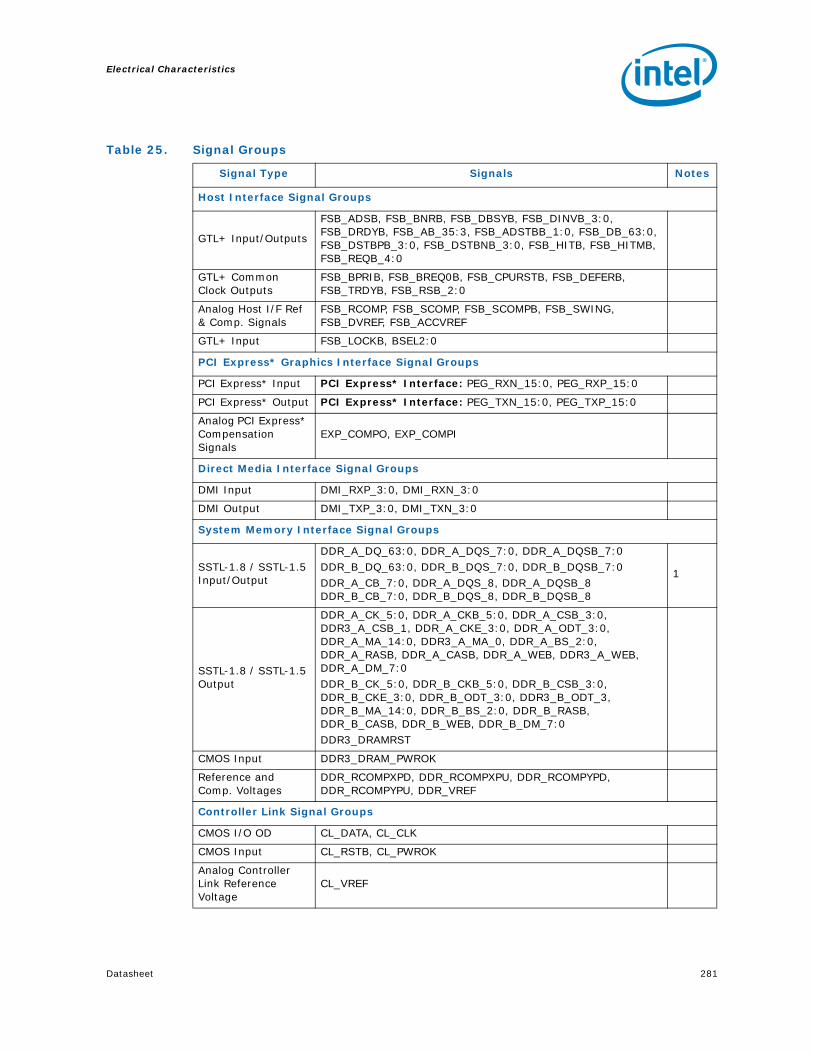
Datasheet 281
Electrical Characteristics
Table 25. Signal Groups
Signal Type Signals Notes
Host Interface Signal Groups
GTL+ Input/Outputs
FSB_ADSB, FSB_BNRB, FSB_DBSYB, FSB_DINVB_3:0, FSB_DRDYB, FSB_AB_35:3, FSB_ADSTBB_1:0, FSB_DB_63:0, FSB_DSTBPB_3:0, FSB_DSTBNB_3:0, FSB_HITB, FSB_HITMB, FSB_REQB_4:0
GTL+ Common Clock Outputs
FSB_BPRIB, FSB_BREQ0B, FSB_CPURSTB, FSB_DEFERB, FSB_TRDYB, FSB_RSB_2:0
Analog Host I/F Ref & Comp. Signals
FSB_RCOMP, FSB_SCOMP, FSB_SCOMPB, FSB_SWING, FSB_DVREF, FSB_ACCVREF
GTL+ Input FSB_LOCKB, BSEL2:0
PCI Express* Graphics Interface Signal Groups
PCI Express* Input PCI Express* Interface: PEG_RXN_15:0, PEG_RXP_15:0
PCI Express* Output PCI Express* Interface: PEG_TXN_15:0, PEG_TXP_15:0
Analog PCI Express* Compensation Signals
EXP_COMPO, EXP_COMPI
Direct Media Interface Signal Groups
DMI Input DMI_RXP_3:0, DMI_RXN_3:0
DMI Output DMI_TXP_3:0, DMI_TXN_3:0
System Memory Interface Signal Groups
SSTL-1.8 / SSTL-1.5 Input/Output
DDR_A_DQ_63:0, DDR_A_DQS_7:0, DDR_A_DQSB_7:0DDR_B_DQ_63:0, DDR_B_DQS_7:0, DDR_B_DQSB_7:0DDR_A_CB_7:0, DDR_A_DQS_8, DDR_A_DQSB_8 DDR_B_CB_7:0, DDR_B_DQS_8, DDR_B_DQSB_8
1
SSTL-1.8 / SSTL-1.5 Output
DDR_A_CK_5:0, DDR_A_CKB_5:0, DDR_A_CSB_3:0, DDR3_A_CSB_1, DDR_A_CKE_3:0, DDR_A_ODT_3:0, DDR_A_MA_14:0, DDR3_A_MA_0, DDR_A_BS_2:0, DDR_A_RASB, DDR_A_CASB, DDR_A_WEB, DDR3_A_WEB, DDR_A_DM_7:0DDR_B_CK_5:0, DDR_B_CKB_5:0, DDR_B_CSB_3:0, DDR_B_CKE_3:0, DDR_B_ODT_3:0, DDR3_B_ODT_3, DDR_B_MA_14:0, DDR_B_BS_2:0, DDR_B_RASB, DDR_B_CASB, DDR_B_WEB, DDR_B_DM_7:0DDR3_DRAMRST
CMOS Input DDR3_DRAM_PWROK
Reference and Comp. Voltages
DDR_RCOMPXPD, DDR_RCOMPXPU, DDR_RCOMPYPD, DDR_RCOMPYPU, DDR_VREF
Controller Link Signal Groups
CMOS I/O OD CL_DATA, CL_CLK
CMOS Input CL_RSTB, CL_PWROK
Analog Controller Link Reference Voltage
CL_VREF
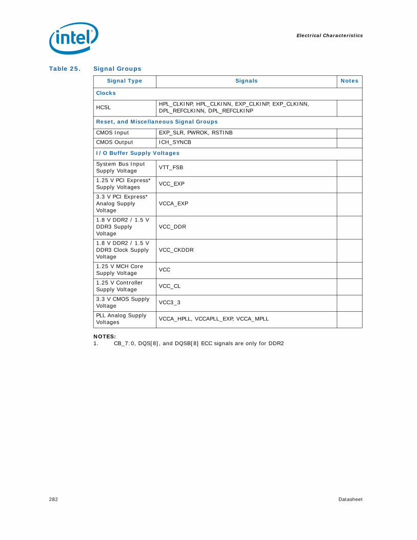
Electrical Characteristics
282 Datasheet
NOTES:1. CB_7:0, DQS[8], and DQSB[8] ECC signals are only for DDR2
Clocks
HCSLHPL_CLKINP, HPL_CLKINN, EXP_CLKINP, EXP_CLKINN, DPL_REFCLKINN, DPL_REFCLKINP
Reset, and Miscellaneous Signal Groups
CMOS Input EXP_SLR, PWROK, RSTINB
CMOS Output ICH_SYNCB
I/O Buffer Supply Voltages
System Bus Input Supply Voltage
VTT_FSB
1.25 V PCI Express* Supply Voltages
VCC_EXP
3.3 V PCI Express* Analog Supply Voltage
VCCA_EXP
1.8 V DDR2 / 1.5 V DDR3 Supply Voltage
VCC_DDR
1.8 V DDR2 / 1.5 V DDR3 Clock Supply Voltage
VCC_CKDDR
1.25 V MCH Core Supply Voltage
VCC
1.25 V Controller Supply Voltage
VCC_CL
3.3 V CMOS Supply Voltage
VCC3_3
PLL Analog Supply Voltages
VCCA_HPLL, VCCAPLL_EXP, VCCA_MPLL
Table 25. Signal Groups
Signal Type Signals Notes
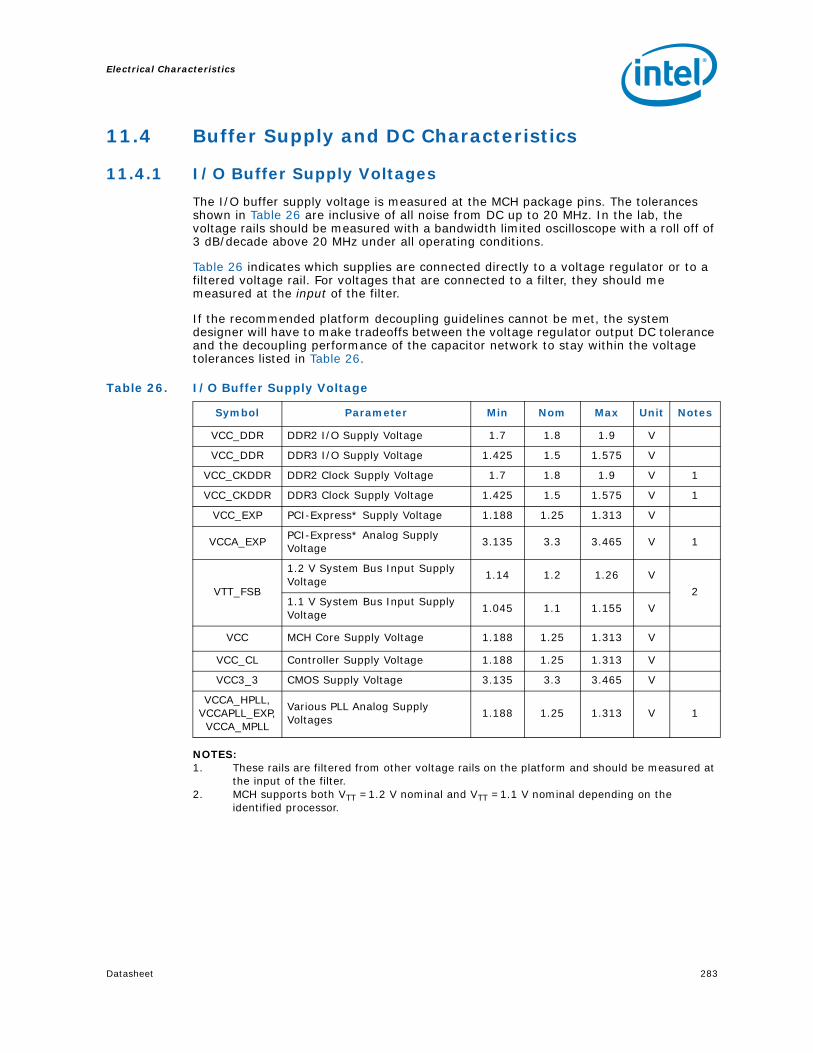
Datasheet 283
Electrical Characteristics
11.4 Buffer Supply and DC Characteristics
11.4.1 I/O Buffer Supply Voltages
The I/O buffer supply voltage is measured at the MCH package pins. The tolerances shown in Table 26 are inclusive of all noise from DC up to 20 MHz. In the lab, the voltage rails should be measured with a bandwidth limited oscilloscope with a roll off of 3 dB/decade above 20 MHz under all operating conditions.
Table 26 indicates which supplies are connected directly to a voltage regulator or to a filtered voltage rail. For voltages that are connected to a filter, they should me measured at the input of the filter.
If the recommended platform decoupling guidelines cannot be met, the system designer will have to make tradeoffs between the voltage regulator output DC tolerance and the decoupling performance of the capacitor network to stay within the voltage tolerances listed in Table 26.
NOTES:1. These rails are filtered from other voltage rails on the platform and should be measured at
the input of the filter. 2. MCH supports both VTT =1.2 V nominal and VTT =1.1 V nominal depending on the
identified processor.
Table 26. I/O Buffer Supply Voltage
Symbol Parameter Min Nom Max Unit Notes
VCC_DDR DDR2 I/O Supply Voltage 1.7 1.8 1.9 V
VCC_DDR DDR3 I/O Supply Voltage 1.425 1.5 1.575 V
VCC_CKDDR DDR2 Clock Supply Voltage 1.7 1.8 1.9 V 1
VCC_CKDDR DDR3 Clock Supply Voltage 1.425 1.5 1.575 V 1
VCC_EXP PCI-Express* Supply Voltage 1.188 1.25 1.313 V
VCCA_EXPPCI-Express* Analog Supply Voltage
3.135 3.3 3.465 V 1
VTT_FSB
1.2 V System Bus Input Supply Voltage
1.14 1.2 1.26 V
21.1 V System Bus Input Supply Voltage
1.045 1.1 1.155 V
VCC MCH Core Supply Voltage 1.188 1.25 1.313 V
VCC_CL Controller Supply Voltage 1.188 1.25 1.313 V
VCC3_3 CMOS Supply Voltage 3.135 3.3 3.465 V
VCCA_HPLL, VCCAPLL_EXP, VCCA_MPLL
Various PLL Analog Supply Voltages
1.188 1.25 1.313 V 1
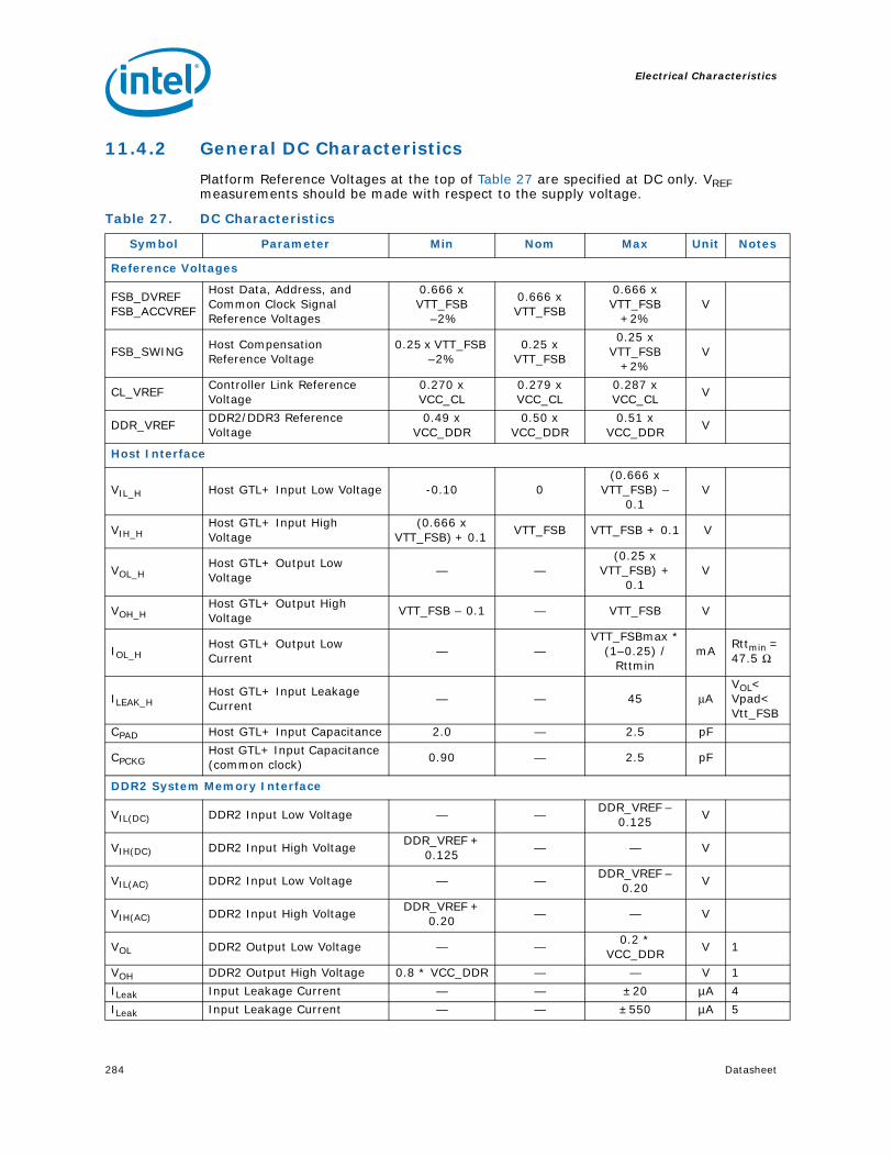
Electrical Characteristics
284 Datasheet
11.4.2 General DC Characteristics
Platform Reference Voltages at the top of Table 27 are specified at DC only. VREF measurements should be made with respect to the supply voltage.
Table 27. DC Characteristics
Symbol Parameter Min Nom Max Unit Notes
Reference Voltages
FSB_DVREF FSB_ACCVREF
Host Data, Address, and Common Clock Signal Reference Voltages
0.666 x VTT_FSB
–2%
0.666 x VTT_FSB
0.666 x VTT_FSB
+2%V
FSB_SWINGHost Compensation Reference Voltage
0.25 x VTT_FSB –2%
0.25 x VTT_FSB
0.25 x VTT_FSB
+2%V
CL_VREFController Link Reference Voltage
0.270 x VCC_CL
0.279 x VCC_CL
0.287 x VCC_CL
V
DDR_VREFDDR2/DDR3 Reference Voltage
0.49 x VCC_DDR
0.50 x VCC_DDR
0.51 xVCC_DDR
V
Host Interface
VIL_H Host GTL+ Input Low Voltage -0.10 0(0.666 x
VTT_FSB) – 0.1
V
VIH_HHost GTL+ Input High Voltage
(0.666 x VTT_FSB) + 0.1
VTT_FSB VTT_FSB + 0.1 V
VOL_HHost GTL+ Output Low Voltage
— —(0.25 x
VTT_FSB) + 0.1
V
VOH_HHost GTL+ Output High Voltage
VTT_FSB – 0.1 — VTT_FSB V
IOL_HHost GTL+ Output Low Current
— —VTT_FSBmax *
(1–0.25) / Rttmin
mARttmin = 47.5 Ω
ILEAK_HHost GTL+ Input Leakage Current
— — 45 μAVOL<Vpad<Vtt_FSB
CPAD Host GTL+ Input Capacitance 2.0 — 2.5 pF
CPCKGHost GTL+ Input Capacitance (common clock)
0.90 — 2.5 pF
DDR2 System Memory Interface
VIL(DC) DDR2 Input Low Voltage — —DDR_VREF –
0.125V
VIH(DC) DDR2 Input High VoltageDDR_VREF +
0.125— — V
VIL(AC) DDR2 Input Low Voltage — —DDR_VREF –
0.20V
VIH(AC) DDR2 Input High VoltageDDR_VREF +
0.20— — V
VOL DDR2 Output Low Voltage — —0.2 *
VCC_DDRV 1
VOH DDR2 Output High Voltage 0.8 * VCC_DDR — — V 1
ILeak Input Leakage Current — — ±20 µA 4
ILeak Input Leakage Current — — ±550 µA 5
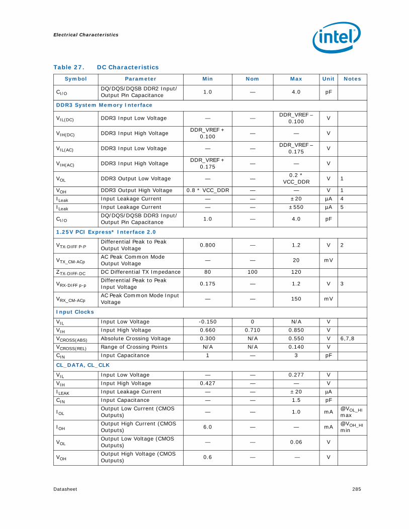
Datasheet 285
Electrical Characteristics
CI/ODQ/DQS/DQSB DDR2 Input/Output Pin Capacitance
1.0 — 4.0 pF
DDR3 System Memory Interface
VIL(DC) DDR3 Input Low Voltage — —DDR_VREF –
0.100V
VIH(DC) DDR3 Input High VoltageDDR_VREF +
0.100— — V
VIL(AC) DDR3 Input Low Voltage — —DDR_VREF –
0.175V
VIH(AC) DDR3 Input High VoltageDDR_VREF +
0.175— — V
VOL DDR3 Output Low Voltage — —0.2 *
VCC_DDRV 1
VOH DDR3 Output High Voltage 0.8 * VCC_DDR — — V 1
ILeak Input Leakage Current — — ±20 µA 4
ILeak Input Leakage Current — — ±550 µA 5
CI/ODQ/DQS/DQSB DDR3 Input/Output Pin Capacitance
1.0 — 4.0 pF
1.25V PCI Express* Interface 2.0
VTX-DIFF P-PDifferential Peak to Peak Output Voltage
0.800 — 1.2 V 2
VTX_CM-ACpAC Peak Common Mode Output Voltage
— — 20 mV
ZTX-DIFF-DC DC Differential TX Impedance 80 100 120
VRX-DIFF p-pDifferential Peak to Peak Input Voltage
0.175 — 1.2 V 3
VRX_CM-ACpAC Peak Common Mode Input Voltage
— — 150 mV
Input Clocks
VIL Input Low Voltage -0.150 0 N/A V
VIH Input High Voltage 0.660 0.710 0.850 V
VCROSS(ABS) Absolute Crossing Voltage 0.300 N/A 0.550 V 6,7,8
VCROSS(REL) Range of Crossing Points N/A N/A 0.140 V
CIN Input Capacitance 1 — 3 pF
CL_DATA, CL_CLK
VIL Input Low Voltage — — 0.277 V
VIH Input High Voltage 0.427 — — V
ILEAK Input Leakage Current — — ± 20 μA
CIN Input Capacitance — — 1.5 pF
IOLOutput Low Current (CMOS Outputs)
— — 1.0 mA@VOL_HI max
IOHOutput High Current (CMOS Outputs)
6.0 — — mA@VOH_HI min
VOLOutput Low Voltage (CMOS Outputs)
— — 0.06 V
VOHOutput High Voltage (CMOS Outputs)
0.6 — — V
Table 27. DC Characteristics
Symbol Parameter Min Nom Max Unit Notes
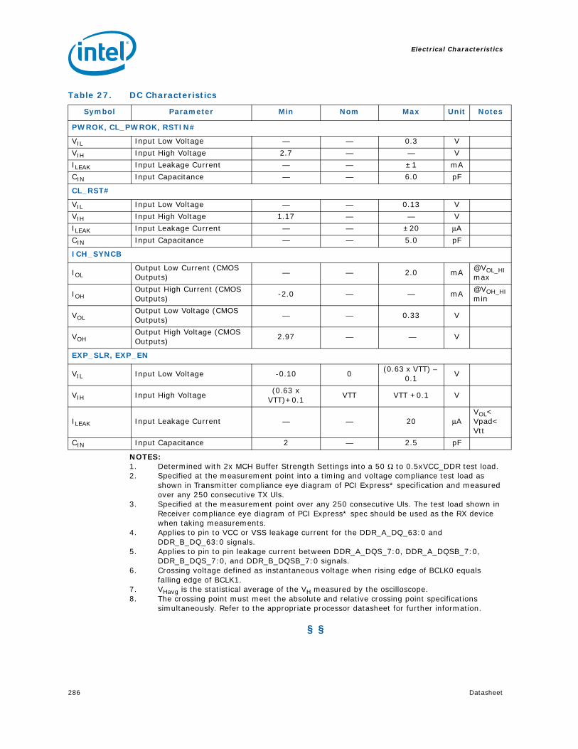
Electrical Characteristics
286 Datasheet
NOTES:1. Determined with 2x MCH Buffer Strength Settings into a 50 Ω to 0.5xVCC_DDR test load. 2. Specified at the measurement point into a timing and voltage compliance test load as
shown in Transmitter compliance eye diagram of PCI Express* specification and measured over any 250 consecutive TX Uls.
3. Specified at the measurement point over any 250 consecutive Uls. The test load shown in Receiver compliance eye diagram of PCI Express* spec should be used as the RX device when taking measurements.
4. Applies to pin to VCC or VSS leakage current for the DDR_A_DQ_63:0 and DDR_B_DQ_63:0 signals.
5. Applies to pin to pin leakage current between DDR_A_DQS_7:0, DDR_A_DQSB_7:0, DDR_B_DQS_7:0, and DDR_B_DQSB_7:0 signals.
6. Crossing voltage defined as instantaneous voltage when rising edge of BCLK0 equals falling edge of BCLK1.
7. VHavg is the statistical average of the VH measured by the oscilloscope.8. The crossing point must meet the absolute and relative crossing point specifications
simultaneously. Refer to the appropriate processor datasheet for further information.
§ §
PWROK, CL_PWROK, RSTIN#
VIL Input Low Voltage — — 0.3 V
VIH Input High Voltage 2.7 — — V
ILEAK Input Leakage Current — — ±1 mA
CIN Input Capacitance — — 6.0 pF
CL_RST#
VIL Input Low Voltage — — 0.13 V
VIH Input High Voltage 1.17 — — V
ILEAK Input Leakage Current — — ±20 μA
CIN Input Capacitance — — 5.0 pF
ICH_SYNCB
IOLOutput Low Current (CMOS Outputs)
— — 2.0 mA@VOL_HI max
IOHOutput High Current (CMOS Outputs)
-2.0 — — mA@VOH_HI min
VOLOutput Low Voltage (CMOS Outputs)
— — 0.33 V
VOHOutput High Voltage (CMOS Outputs)
2.97 — — V
EXP_SLR, EXP_EN
VIL Input Low Voltage -0.10 0(0.63 x VTT) –
0.1 V
VIH Input High Voltage(0.63 x
VTT)+0.1 VTT VTT +0.1 V
ILEAK Input Leakage Current — — 20 μAVOL<Vpad<Vtt
CIN Input Capacitance 2 — 2.5 pF
Table 27. DC Characteristics
Symbol Parameter Min Nom Max Unit Notes

Datasheet 287
Ballout and Package Information
12 Ballout and Package Information
This chapter provides the ballout and package dimensions for the MCH.
12.1 Ballout Information
Figure 11, Figure 12, and Figure 13 provide the MCH ballout as viewed from the top side of the package. Table 28 provides a ballout list arranged alphabetically by signal name. Table 29 provides a ballout list arranged numerically by ball number.
Note: Notes for Figure 11, Figure 12, Figure 13, Table 28 and Table 29.
1. Balls that are listed as RSVD are reserved.
2. Some balls marked as reserved (RSVD) are used in XOR testing. See Chapter 13 for details.
3. Balls that are listed as NC are No Connects.

Ballout and Package Information
288 Datasheet
Figure 11. MCH Ballout Diagram (Top View Left – Columns 45–31)45 44 43 42 41 40 39 38 37 36 35 34 33 32 31
BE TEST0 VCC_CKDDR VCC_CKDDR VCC_DDR VSS VCC_DDR VSS VCC_DDR BE
BD NC VCC_CKDDR VCC_CKDDR DDR_A_CSB_1
DDR_A_WEB
DDR_A_MA_10
DDR3_A_MA0
DDR_B_ODT_0
DDR_B_RASB BD
BC VCC_CKDDR VCC_CKDDR VSS DDR_RCOMPYPD
DDR3_A_WEB VCC_DDR DDR_A_
BS_0DDR_A_MA_0 VCC_DDR DDR_B_CSB
_2 BC
BBDDR3_A_CS
B_1DDR_A_ODT
_0DDR_RCOM
PYPUDDR_A_CAS
BDDR_A_CSB_2
DDR_A_RASB
DDR_A_BS_1
DDR_B_CSB_1
DDR_B_ODT_1
DDR_B_ODT_2
DDR_B_CASB
DDR_A_MA_1 BB
BADDR_A_MA_13
DDR_A_ODT_2
DDR_A_CSB_0
DDR3_B_ODT3
DDR_B_CSB_3
DDR_B_MA_13
DDR_B_CSB_0 BA
AY VCC_DDR DDR_A_CSB_3
DDR_A_ODT_1
DDR_B_DM_4
DDR_B_DQ_32
DDR_B_DQ_36 VSS DDR_B_
ODT_3DDR_B_CKB_5 VSS DDR_B_
WEB AY
AWDDR_A_ODT
_3DDR_A_DQ_
36 VSS DDR_B_DQS_4
DDR_B_DQ_33
DDR_B_DQ_37 VSS DDR_B_
CK_5DDR_B_CKB_2 VSS AW
AV VSS VSS DDR_A_DQ_32
DDR_B_DQ_39
DDR_B_DQ_38
DDR_B_DQSB_4
DDR_B_DQ_44
DDR_A_CKB_2 VSS DDR_B_
CK_2DDR_A_
CK_3 AV
AUDDR_A_DM_4
DDR_A_DQ_33
DDR_A_DQ_37 AU
AT VSS DDR_A_DQS_4
DDR_A_DQSB_4
DDR_B_DQ_35 VSS DDR_B_
DQ_34DDR_A_CKB_5
DDR_A_CK_5
DDR_A_CK_2
DDR_A_CK_0
DDR_A_CKB_3 AT
ARDDR_A_DQ_34
DDR_A_DQ_35
DDR_A_DQ_38
DDR_A_DQ_39 VSS VSS DDR_B_
DQ_40 VSS DDR_B_DQ_45
DDR_A_CKB_0
DDR_B_CK_3 AR
APDDR_A_DQ_45 VSS DDR_A_
DQ_44DDR_B_DQSB_5
DDR_B_DQS_5 VSS DDR_B_DQ_
41DDR_B_DQ_42 RSVD VSS DDR_B_
CKB_3 AP
ANDDR_A_DM_5
DDR_A_DQ_41
DDR_A_DQ_40
DDR_B_DQ_47
DDR_B_DQ_46 VSS DDR_B_
DM_5DDR_A_
CB_1 VSS DDR_B_DQ_43 RSVD AN
AM VSS DDR_A_DQS_5
DDR_A_DQSB_5 RSVD AM
ALDDR_A_DQ_42
DDR_A_DQ_43
DDR_A_DQ_47
DDR_A_DQ_46 VSS DDR_A_DQ
S_8DDR_A_DQSB_8 VSS DDR_A_
CB_5DDR_A_
CB_0 AL
AKDDR_B_
CB_0 VSS DDR_B_CB_5 VSS DDR_A_
CB_7DDR_A_
CB_2 VSS DDR_A_CB_3
DDR_A_CB_6
DDR_A_CB_4 VSS VCC_CL AK
AJDDR_B_
CB_1DDR_B_
CB_4 VSS AJ
AH VSS DDR_B_DQS_8
DDR_B_DQSB_8 VSS VSS VSS DDR_B_
DQ_53 VSS DDR_B_DQ_48
DDR_B_DQ_52 VSS VCC_CL AH
AGDDR_B_CB_
7DDR_B_CB_
2DDR_B_CB_
6DDR_B_CB_
3DDR_B_DQ
S_6DDR_B_DQ
SB_6 VSS DDR_B_DM_6 VSS DDR_B_
DQ_49 RSVD VCC_CL AG
AFDDR_A_DQ_53 VSS DDR_A_DQ_
52 AF
AEDDR_A_DM_6
DDR_A_DQ_49
DDR_A_DQ_48
DDR_B_DQ_54
DDR_B_DQ_50
DDR_B_DQ_51 VSS DDR_B_DQ_
60DDR_B_DQ_
61DDR_B_DQ_
55 VSS VCC_CL AE
AD VSS DDR_A_DQS_6
DDR_A_DQSB_6
DDR_A_DQ_54
DDR_B_DQ_56 VSS DDR_B_
DQ_57DDR_B_DM_7 VSS DDR_B_
DQSB_7 RSVD VCC_CL AD
ACDDR_A_DQ_51 VSS DDR_A_
DQ_50DDR_A_DQ_60
DDR_A_DQ_55 VSS DDR_B_
DQ_62 VSS DDR_B_DQ_63
DDR_B_DQS_7 VSS VCC_CL AC
AB VSS DDR_A_DQ_57
DDR_A_DQ_56
DDR_A_DM_7
DDR_A_DQ_61
DDR_B_DQ_59 VSS FSB_AB_34 FSB_AB_29 VSS DDR_B_
DQ_58 VCC_CL AB
AADDR_A_DQSB_7
DDR_A_DQS_7
DDR_A_DQ_62 FSB_AB_33 VSS FSB_AB_35 VSS FSB_AB_32 VSS FSB_AB_31 VSS VCC_CL AA
YDDR_A_DQ_63 VSS DDR_A_
DQ_58 Y
WFSB_
BREQ0BDDR_A_DQ_59 FSB_RSB_1 FSB_TRDYB VSS FSB_AB_22 FSB_AB_30 VSS FSB_AB_25 FSB_AB_27 RSVD VSS_W31 W
V VSS FSB_AB_28 FSB_HITMB VSS FSB_AB_24 FSB_AB_23 VSS FSB_AB_26 FSB_ADSTBB_1 VSS RSVD VCC_CL V
U FSB_ADSB FSB_BNRB FSB_DRDYB U
T FSB_LOCKB VSS FSB_DBSYB FSB_AB_17 FSB_DEFERB FSB_AB_20 FSB_AB_18 VSS FSB_AB_19 RSVD VSS VCCAUX T
R FSB_RSB_0 FSB_HITB FSB_RSB_2 VSS FSB_AB_14 VSS FSB_AB_10 FSB_AB_16 VSS RSVD R
P VSS FSB_AB_21 FSB_DB_0 VSS P
N FSB_DB_2 FSB_DB_4 FSB_DB_1 FSB_AB_9 FSB_AB_11 FSB_AB_13 FSB_AB_8 VSS FSB_AB_12 FSB_DB_28 FSB_DB_30 N
M FSB_DB_5 VSS FSB_DB_3 FSB_ADSTBB_0 VSS FSB_AB_4 FSB_AB_5 VSS VSS VSS FSB_DB_31 M
L FSB_DB_6 FSB_DB_7 FSB_DINVB_0 FSB_AB_7 FSB_
REQB_2 VSS FSB_DB_19 VSS FSB_DB_27 FSB_DB_29 VSS L
K VSS FSB_DSTBNB_0 FSB_AB_15 VSS VSS FSB_AB_6 FSB_
REQB_3 FSB_DB_21 FSB_DB_24 VSS FSB_DB_33 K
JFSB_
DSTBPB_0 FSB_DB_8 FSB_DB_10 J
H FSB_DB_12 VSS FSB_DB_9 VSS FSB_REQB_4 FSB_BPRIB VSS VSS FSB_
DSTBPB_1 FSB_DB_25 FSB_DB_34 H
G FSB_DB_13 FSB_DB_11 FSB_REQB_1 VSS FSB_DB_20 FSB_DB_22 FSB_DB_23 FSB_
DSTBNB_1 VSS VSS G
F VSS FSB_AB_3 FSB_DB_14 VSS FSB_DB_17 FSB_DB_16 VSS FSB_DB_48 VSS FSB_DB_26 FSB_DB_32 F
E FSB_DB_15 FSB_DB_50 FSB_DINVB_1 FSB_DB_61 FSB_DB_63 VTT_FSB VTT_FSB E
D FSB_DB_52 FSB_DB_53 VSS FSB_DSTBNB_3 FSB_DB_57 FSB_DB_54 FSB_DB_59 FSB_
CPURSTB VSS VTT_FSB VTT_FSB VTT_FSB D
C VSS FSB_REQB_0 VSS FSB_DB_51 FSB_
DSTBPB_3 VSS FSB_DB_60 FSB_DB_58 VSS VTT_FSB C
B NC VSS FSB_DB_18 FSB_DB_55 FSB_DB_56 FSB_DINVB_3 FSB_DB_62 VTT_FSB VTT_FSB B
A TEST3 NC VSS VSS FSB_DB_49 VSS VSS VTT_FSB A
45 44 43 42 41 40 39 38 37 36 35 34 33 32 31

Datasheet 289
Ballout and Package Information
Figure 12. MCH Ballout Diagram (Top View Middle – Columns 30–16)
30 29 28 27 26 25 24 23 22 21 20 19 18 17 16
BE VSS VCC_DDR VSS VCC_DDR VSS VCC_DDR DDR_B_MA_8 VSS DDR_A_
DQ_19 BE
BDDDR_A_MA_6
DDR_A_MA_11
DDR_A_CKE_0
DDR_B_MA_4
DDR_B_CKE_1
DDR_B_CKE_0 BD
BC VCC_DDR DDR_A_MA_8 VCC_DDR DDR_A_
CKE_3 VCC_DDR DDR_B_MA_1 VCC_DDR DDR_B_
MA_14 VSS BC
BBDDR_A_
MA_2DDR_A_MA_3
DDR_A_MA_5
DDR_A_MA_12
DDR_A_BS_2
DDR_A_CKE_2
DDR_B_BS_0
DDR3_DRAMRSTB
DDR_B_MA_2
DDR_B_MA_5
DDR_B_MA_6
DDR_B_MA_9
DDR_B_BS_2
DDR_B_CKE_2
DDR_A_DQ_18 BB
BADDR_A_MA_4
DDR_A_MA_9
DDR_A_MA_14
DDR_B_MA_3
DDR_B_MA_11
DDR_B_CKE_3 BA
AYDDR_B_
CK_4DDR_B_CKB_4
DDR_A_MA_7
DDR_B_DM_3
DDR_A_CKE_1 VCC_DDR DDR_B_
MA_0DDR_A_DQ_25
DDR_B_MA_7
DDR_B_MA_12
DDR_B_DQ_16 AY
AWDDR_B_
CK_0 VSS VSS DDR_B_DQ_24
DDR_B_MA_10
DDR_B_BS_1
DDR_A_DQ_31 VSS DDR_A_
DQ_29 VSS DDR_B_DM_2 AW
AVDDR_B_CKB_0 VSS DDR_B_
DQ_27DDR_B_DQ_25 VSS VSS VSS DDR_A_
DQSB_3DDR_A_DQ_28 VSS DDR_B_
DQ_17 AV
AU AU
AT VSS VSS DDR_B_DQ_26
DDR_B_DQ_30 VSS VSS DDR_A_
DQ_27DDR_A_DQS_3
DDR_B_DQ_19
DDR_B_DQ_22 VSS AT
AR VSS DDR_B_CK_1 VSS DDR_B_
DQS_3DDR_B_DQSB_3 VSS VSS VSS VSS DDR_B_
DQ_23DDR_B_DQ_21 AR
AP VSS DDR_B_CKB_1
DDR_B_DQ_31 VSS DDR_B_
DQ_29 VSS VSS DDR_A_DM_3
DDR_B_DQ_18 VSS DDR_B_
DQSB_2 AP
AN RSVD DDR_A_CK_1
DDR_A_CK_4 RSVD DDR_B_
DQ_28 VSS DDR_A_DQ_26
DDR_A_DQ_30
DDR_A_DQ_24
DDR_B_DQS_2
DDR_B_DQ_20 AN
AM VCC_CL DDR_A_CKB_1
DDR_A_CKB_4 RSVD VSS VCC_CL VCC_CL VSS PWROK RSTINB VSS AM
AL VCC_CL RSVD VCC_CL VCC_CL VCC_CL VCC_CL VCC_CL VCC_CL VCC_CL VCC_CL VCC_CL AL
AK AK
AJ VCC_CL VCC_CL VCC_CL VCC_CL VCC_CL VCC_CL VCC_CL VCC_CL VCC_CL VCC_CL VCC_CL VCC_CL VCC_CL AJ
AH VCC_CL RSVD VSS VCC VSS VCC VSS VCC VSS VCC VCC VCC VCC AH
AG VCC_CL RSVD VCC VSS VCC VSS VCC VSS VCC VSS VCC VCC VCC AG
AF VCC_CL VCC VSS VCC VSS VCC VSS VCC VSS VCC VSS VCC VCC AF
AE VCC_CL VCC VCC VSS VCC VSS VCC VSS VCC VSS VCC VCC VCC AE
AD VCC_CL VCC VSS VCC VSS VCC VSS VCC VSS VCC VSS VCC VCC AD
AC VCC_CL VCC VCC VSS VCC VSS VCC VSS VCC VSS VCC VCC VCC AC
AB VCC_CL VCC VSS VCC VSS VCC VSS VCC VSS VCC VSS VCC VCC AB
AA VCC_CL VCC VCC VSS VCC VSS VCC VSS VCC VSS VCC VCC VCC AA
Y VCC_CL VCC VSS VCC VSS VCC VSS VCC VSS VCC VSS VCC VCC Y
W VCC_CL VCC VCC VSS VCC VSS VCC VSS VCC VSS VCC VCC VCC W
V VCC_CL VCC VSS VCC VSS VCC VSS VCC VSS VCC VSS VCC VCC V
U VCCAUX VCC VCC VCC VCC VCC VCC VCC VCC VCC VCC VCC VCC U
T T
R VCCAUX VCCAUX VCCAUX VCCAUX VCCAUX VCCAUX RSVD VSS RSVD VCC VCC R
PHPL_
CLKINN HPL_CLKINP VSS VSS VSS VSS VSS RSVD RSVD_P19 VSS ICH_SYNCB P
N FSB_DB_37 FSB_DINVB_2 VSS FSB_
DSTBPB_2 FSB_DB_42 VSS VSS RSVD VSS RSVD VSS N
M FSB_DB_35 VSS VTT_FSB FSB_DSTBNB_2 VSS VSS BSEL0 ALLZTEST RSVD_M19 VSS RSVD M
L FSB_DB_36 FSB_DB_41 VTT_FSB FSB_DB_43 FSB_DB_44 VSS XORTEST VSS RSVD RSVD VCC3_3_L16 L
K VSS FSB_DB_40 VTT_FSB VTT_FSB FSB_DB_46 VSS RSVD RSVD EXP_SLR VSS RSVD_K16 K
J J
H FSB_DB_39 VTT_FSB VTT_FSB VTT_FSB FSB_DB_45 VSS VSS RSVD VSS VSS RSVD_H16 H
G FSB_DB_38 VTT_FSB VTT_FSB VTT_FSB FSB_DB_47 VSS RSVD TCEN MTYPE VSS VCC3_3_G16 G
F VTT_FSB VTT_FSB VTT_FSB VTT_FSB VSS VSS VSS_F22 BSEL1 RSVD BSEL2 VSS F
E VTT_FSB FSB_DVREF VCC_E25 VSS VSS PEG_TXN_0 E
D VTT_FSB VSS FSB_SCOMP FSB_ACCVREF VCCA_HPL VCCA_HPL VSS_D24 VSS VSS_D22 VSS_D21 VCCA_EXP EXP_CLKINP EXP_CLKIN
N VSS PEG_TXP_0 D
C VSS FSB_SCOMPB FSB_RCOMP VSS_C24 VSS_C23 VSS VSS VCC_C18 VCCR_EXP C
B VSS VCCA_MPL VCC_B25 VSS_B21 RSVD VSS_B17 B
A VTT_FSB FSB_SWING VSS VSS_A24 VCC3_3 VSS VCCAPLL_EXP VSS PEG_RXP_0 A
30 29 28 27 26 25 24 23 22 21 20 19 18 17 16

Ballout and Package Information
290 Datasheet
Figure 13. MCH Ballout Diagram (Top View Left – Columns 15–1)15 14 13 12 11 10 9 8 7 6 5 4 3 2 1
BE VSS DDR_A_DQ_11 VSS DDR_A_
DQ_3 VSS VSS NC TEST1 BE
BDDDR_A_DQ_22
DDR_A_DQ_16
DDR_A_DQ_14
DDR_A_DQ_8
DDR_A_DQ_6
DDR_A_DQ_1
DDR_A_DQ_4 VSS NC BD
BCDDR_A_DM_2 VSS DDR_A_
DM_1DDR_A_DQ_13 VSS DDR_A_DQ
SB_0DDR_A_DQ_0 VSS RSVD VSS BC
BBDDR_A_DQ_23
DDR_A_DQ_17
DDR_A_DQ_21
DDR_A_DQ_10
DDR_A_DQ_15
DDR_A_DQ_9
DDR_A_DQ_2
DDR_A_DQ_7
DDR_A_DM_0
DDR_A_DQ_5 VSS_BB3 VSS BB
BADDR_A_DQS_2
DDR_A_DQ_20
DDR_A_DQS_1
DDR_A_DQ_12
DDR_A_DQS_0 VSS_BA5 VSS_BA4 BA
AYDDR_A_DQSB_2
DDR_B_DQ_9
DDR_B_DQ_8
DDR_A_DQSB_1 VSS DDR_B_
DM_0DDR_B_DQ_1
DDR_RCOMPXPD
DDR_RCOMPXPU VSS_AY3 VSS_AY1 AY
AW VSS DDR_B_DQ_13
DDR_B_DQ_12
DDR_B_DQ_7
DDR_B_DQS_0
DDR_B_DQ_0 VSS DDR_B_
DQ_5 VSS VSS_AW2 AW
AVDDR_B_DQ_11 VSS VSS VSS VSS DDR_B_
DQ_4 DDR_VREF VSS VSS VSS VSS AV
AU VCCA_EXP2 VSS PEG2_TXP_14 AU
ATDDR_B_DQ_10
DDR_B_DM_1
DDR_B_DQ_3
DDR_B_DQ_2
DDR_B_DQSB_0 VSS DDR_
RCOMPVOLDDR_RCOM
PVOHPEG2_TXP_13
PEG2_TXN_14 VSS AT
AR VSS DDR_B_DQS_1
DDR_B_DQSB_1
DDR_B_DQ_6
VCCAPLL_EXP2 VSS VSS VSS PEG2_
TXN_13 VSS PEG2_TXP_12 AR
APDDR_B_DQ_15 VSS RSVD PEG2_
RXN_15PEG2_RXP_15 VSS PEG2_
TXP_15PEG2_TXN_15
PEG2_TXP_11 VCCR_EXP PEG2_TXN_
12 AP
ANDDR_B_DQ_14 RSVD RSVD DDR3_DRA
M_PWROKEXP2_COMPI
EXP2_COMPO VSS VSS PEG2_
TXN_11 VSS PEG2_TXP_10 AN
AM RSVD PEG2_TXP_9
PEG2_TXN_10 VSS AM
AL CL_PWROK VSS PEG2_RXP_13
PEG2_RXN_13 VSS PEG2_
RXN_14PEG2_RXP_14
PEG2_TXN_9 VSS PEG2_TXP_
8 AL
AK CL_DATA CL_CLK PEG2_RXN_12
PEG2_RXP_12 VSS VSS VSS VSS VSS PEG2_
TXP_7 VCCR_EXP PEG2_TXN_8 AK
AJPEG2_TXN_7 VSS PEG2_TXP_
6 AJ
AH VCC_CL VCC_CL PEG2_RXN_9 VSS PEG2_
RXP_10PEG2_
RXN_10 VSS PEG2_RXP_11
PEG2_RXN_11
PEG2_TXP_5
PEG2_TXN_6 VSS AH
AG VCC CL_VREF VSS PEG2_RXP_9 CL_RSTB VSS VSS VSS VSS PEG2_
TXN_5 VSS PEG2_TXP_4 AG
AFPEG2_TXP_
3 VCCR_EXP PEG2_TXN_4 AF
AE VCCR_EXP EXP2_CLKINP
PEG2_RXP_6 VSS PEG2_
RXN_7PEG2_RXP_7 VSS PEG2_
RXP_8PEG2_RXN_8
PEG2_TXN_3 VSS PEG2_TXP_
2 AE
AD VCCR_EXP EXP2_CLKINN VSS PEG2_
RXN_6 VCC_EXP VCC_EXP VCC_EXP VCC_EXP VSS PEG2_TXP_1
PEG2_TXN_2 VSS AD
AC VCCR_EXP VSS PEG2_RXP_3 VSS PEG2_
RXP_4PEG2_RXN_4 VSS PEG2_
RXN_5PEG2_RXP_5
PEG2_TXN_1 VCCR_EXP VSS AC
AB VCC VCCR_EXP VCC_EXT_PLL
PEG2_RXN_3 VCC_EXP VCC_EXP VCC_EXP VCC_EXP VCC_EXP VCC_EXP PEG2_TXP_
0PEG2_TXN_
0 AB
AA VCCR_EXP VCCR_EXP PEG2_RXN_0 VSS PEG2_
RXN_1PEG2_RXP_1 VSS PEG2_RXN_
2PEG2_RXP_
2 VCC_EXP VCC_EXP VCC_EXP AA
Y VCC_EXP VCC_EXP VCC_EXP Y
W VCCR_EXP VSS VSS PEG2_RXP_0 VCC_EXP VCC_EXP VCC_EXP VCC_EXP VSS VCC_EXP VCC_EXP VCC_EXP W
V VCCR_EXP VCCR_EXP VSS RSVD DMI_TXN_3 DMI_TXP_3 VSS DMI_RXP_3 DMI_RXN_3 VCC_EXP VCC_EXP VCC_EXP V
U VCC_EXP VCC_EXP VCC_EXP U
T VCCR_EXP VCCR_EXP VSS RSVD VSS EXP_COMPO DMI_RXN_1 DMI_RXP_1 VSS VCC_EXP VCC_EXP DMI_TXN_2 T
R VSS VSS VSS EXP_COMPI VSS DMI_TXP_0 DMI_TXN_0 DMI_RXN_2 VSS DMI_TXP_2 R
P VSS DMI_RXP_2 DMI_TXN_1 VSS P
N VCC_N15 PEG_RXP_4 RSVD RSVD PEG_RXN_15
PEG_RXP_15 VSS VSS DMI_RXP_0 VSS DMI_TXP_1 N
M VSS_M15 PEG_RXN_4 VSS PEG_RXP_12 VSS PEG_
RXN_13PEG_
RXP_13 VSS DMI_RXN_0 VCCR_EXP PEG_TXP_15 M
L VSS PEG_RXP_3 PEG_RXN_6 VSS PEG_RXN_12 VSS VSS VSS PEG_
TXP_14 VSS PEG_TXN_15 L
K VSS PEG_RXN_3 VSS PEG_RXP_6 VSS PEG_RXN_11
PEG_RXP_11 VSS PEG_
TXN_14PEG_
RXP_14 VSS K
JPEG_
TXP_13 VSS PEG_RXN_14 J
H RSVD_H15 PEG_RXP_2 PEG_RXP_5 VSS PEG_RXN_7 VSS VSS VSS PEG_TXN_13 VCCR_EXP PEG_
TXP_12 H
G RSVD_G15 PEG_RXN_2 PEG_RXN_5 VSS PEG_RXP_7 VSS VSS PEG_RXN_9 VSS PEG_TXN_12 G
F VSS VSS VSS VSS VSS VSS PEG_RXP_9 VSS PEG_TXP_11
PEG_TXP_10 VSS F
E PEG_TXP_1 PEG_TXP_2 PEG_TXN_4 PEG_TXN_6 PEG_RXP_8 VSS PEG_TXN_11 E
D VSS PEG_TXN_1 VSS PEG_TXN_2 VSS PEG_TXP_4 PEG_TXP_6 VSS PEG_RXN_8 VSS PEG_TXN_10
PEG_RXP_10 D
C PEG_RXN_1 VCCR_EXP PEG_TXN_5 VSS VCCR_EXP PEG_TXP_8 PEG_TXN_8 VSS PEG_RXN_10 VSS C
B PEG_RXN_0 PEG_RXP_1 PEG_TXP_3 PEG_TXP_5 PEG_TXP_7 PEG_TXN_9 PEG_TXP_9 VSS NC B
A VSS PEG_TXN_3 VSS PEG_TXN_7 VSS VSS TEST2 A
15 14 13 12 11 10 9 8 7 6 5 4 3 2 1

Datasheet 291
Ballout and Package Information
Table 28. MCH Ballout Sorted By Name
Signal Name Ball #
ALLZTEST M21
BSEL0 M22
BSEL1 F21
BSEL2 F18
CL_CLK AK14
CL_DATA AK15
CL_PWROK AL13
CL_RSTB AG11
CL_VREF AG14
DDR_A_BS_0 BC37
DDR_A_BS_1 BB36
DDR_A_BS_2 BB26
DDR_A_CASB BB41
DDR_A_CB_0 AL33
DDR_A_CB_1 AN35
DDR_A_CB_2 AK38
DDR_A_CB_3 AK35
DDR_A_CB_4 AK33
DDR_A_CB_5 AL34
DDR_A_CB_6 AK34
DDR_A_CB_7 AK39
DDR_A_CK_0 AT33
DDR_A_CK_1 AN28
DDR_A_CK_2 AT34
DDR_A_CK_3 AV31
DDR_A_CK_4 AN27
DDR_A_CK_5 AT35
DDR_A_CKB_0 AR33
DDR_A_CKB_1 AM28
DDR_A_CKB_2 AV35
DDR_A_CKB_3 AT31
DDR_A_CKB_4 AM27
DDR_A_CKB_5 AT36
DDR_A_CKE_0 BD25
DDR_A_CKE_1 AY24
DDR_A_CKE_2 BB25
DDR_A_CKE_3 BC24
DDR_A_CSB_0 BA40
DDR_A_CSB_1 BD42
DDR_A_CSB_2 BB39
DDR_A_CSB_3 AY43
DDR_A_DM_0 BB5
DDR_A_DM_1 BC10
DDR_A_DM_2 BC14
DDR_A_DM_3 AP21
DDR_A_DM_4 AU44
DDR_A_DM_5 AN44
DDR_A_DM_6 AE44
DDR_A_DM_7 AB40
DDR_A_DQ_0 BC4
DDR_A_DQ_1 BD4
DDR_A_DQ_2 BB8
DDR_A_DQ_3 BE8
DDR_A_DQ_4 BD3
DDR_A_DQ_5 BB4
DDR_A_DQ_6 BD7
DDR_A_DQ_7 BB7
DDR_A_DQ_8 BD9
DDR_A_DQ_9 BB10
DDR_A_DQ_10 BB12
DDR_A_DQ_11 BE12
DDR_A_DQ_12 BA9
DDR_A_DQ_13 BC9
DDR_A_DQ_14 BD11
DDR_A_DQ_15 BB11
DDR_A_DQ_16 BD13
DDR_A_DQ_17 BB14
DDR_A_DQ_18 BB16
DDR_A_DQ_19 BE16
DDR_A_DQ_20 BA13
DDR_A_DQ_21 BB13
DDR_A_DQ_22 BD15
DDR_A_DQ_23 BB15
DDR_A_DQ_24 AN19
DDR_A_DQ_25 AY21
DDR_A_DQ_26 AN22
DDR_A_DQ_27 AT22
DDR_A_DQ_28 AV19
DDR_A_DQ_29 AW19
DDR_A_DQ_30 AN21
DDR_A_DQ_31 AW22
DDR_A_DQ_32 AV42
DDR_A_DQ_33 AU43
DDR_A_DQ_34 AR44
DDR_A_DQ_35 AR42
DDR_A_DQ_36 AW42
DDR_A_DQ_37 AU41
DDR_A_DQ_38 AR41
DDR_A_DQ_39 AR40
DDR_A_DQ_40 AN41
Table 28. MCH Ballout Sorted By Name
Signal Name Ball #
DDR_A_DQ_41 AN42
DDR_A_DQ_42 AL44
DDR_A_DQ_43 AL42
DDR_A_DQ_44 AP42
DDR_A_DQ_45 AP45
DDR_A_DQ_46 AL40
DDR_A_DQ_47 AL41
DDR_A_DQ_48 AE41
DDR_A_DQ_49 AE42
DDR_A_DQ_50 AC42
DDR_A_DQ_51 AC45
DDR_A_DQ_52 AF42
DDR_A_DQ_53 AF45
DDR_A_DQ_54 AD40
DDR_A_DQ_55 AC39
DDR_A_DQ_56 AB42
DDR_A_DQ_57 AB43
DDR_A_DQ_58 Y42
DDR_A_DQ_59 W42
DDR_A_DQ_60 AC40
DDR_A_DQ_61 AB39
DDR_A_DQ_62 AA41
DDR_A_DQ_63 Y45
DDR_A_DQS_0 BA6
DDR_A_DQS_1 BA11
DDR_A_DQS_2 BA15
DDR_A_DQS_3 AT21
DDR_A_DQS_4 AT43
DDR_A_DQS_5 AM43
DDR_A_DQS_6 AD43
DDR_A_DQS_7 AA42
DDR_A_DQS_8 AL38
DDR_A_DQSB_0 BC6
DDR_A_DQSB_1 AY11
DDR_A_DQSB_2 AY15
DDR_A_DQSB_3 AV21
DDR_A_DQSB_4 AT42
DDR_A_DQSB_5 AM42
DDR_A_DQSB_6 AD42
DDR_A_DQSB_7 AA44
DDR_A_DQSB_8 AL36
DDR_A_MA_0 BC36
DDR_A_MA_1 BB31
DDR_A_MA_2 BB30
DDR_A_MA_3 BB29
Table 28. MCH Ballout Sorted By Name
Signal Name Ball #

292 Datasheet
Ballout and Package Information
DDR_A_MA_4 BA29
DDR_A_MA_5 BB28
DDR_A_MA_6 BD29
DDR_A_MA_7 AY27
DDR_A_MA_8 BC28
DDR_A_MA_9 BA27
DDR_A_MA_10 BD37
DDR_A_MA_11 BD27
DDR_A_MA_12 BB27
DDR_A_MA_13 BA42
DDR_A_MA_14 BA25
DDR_A_ODT_0 BB43
DDR_A_ODT_1 AY41
DDR_A_ODT_2 BA41
DDR_A_ODT_3 AW44
DDR_A_RASB BB38
DDR_A_WEB BD39
DDR_B_BS_0 BB24
DDR_B_BS_1 AW23
DDR_B_BS_2 BB18
DDR_B_CASB BB32
DDR_B_CB_0 AK45
DDR_B_CB_1 AJ44
DDR_B_CB_2 AG42
DDR_B_CB_3 AG40
DDR_B_CB_4 AJ42
DDR_B_CB_5 AK42
DDR_B_CB_6 AG41
DDR_B_CB_7 AG44
DDR_B_CK_0 AW30
DDR_B_CK_1 AR28
DDR_B_CK_2 AV33
DDR_B_CK_3 AR31
DDR_B_CK_4 AY30
DDR_B_CK_5 AW34
DDR_B_CKB_0 AV30
DDR_B_CKB_1 AP28
DDR_B_CKB_2 AW33
DDR_B_CKB_3 AP31
DDR_B_CKB_4 AY28
DDR_B_CKB_5 AY34
DDR_B_CKE_0 BD17
DDR_B_CKE_1 BD19
DDR_B_CKE_2 BB17
DDR_B_CKE_3 BA17
Table 28. MCH Ballout Sorted By Name
Signal Name Ball #
DDR_B_CSB_0 BA31
DDR_B_CSB_1 BB35
DDR_B_CSB_2 BC32
DDR_B_CSB_3 BA35
DDR_B_DM_0 AY8
DDR_B_DM_1 AT13
DDR_B_DM_2 AW16
DDR_B_DM_3 AY25
DDR_B_DM_4 AY40
DDR_B_DM_5 AN36
DDR_B_DM_6 AG35
DDR_B_DM_7 AD35
DDR_B_DQ_0 AW8
DDR_B_DQ_1 AY7
DDR_B_DQ_2 AT11
DDR_B_DQ_3 AT12
DDR_B_DQ_4 AV8
DDR_B_DQ_5 AW6
DDR_B_DQ_6 AR11
DDR_B_DQ_7 AW11
DDR_B_DQ_8 AY12
DDR_B_DQ_9 AY13
DDR_B_DQ_10 AT15
DDR_B_DQ_11 AV15
DDR_B_DQ_12 AW12
DDR_B_DQ_13 AW13
DDR_B_DQ_14 AN15
DDR_B_DQ_15 AP15
DDR_B_DQ_16 AY16
DDR_B_DQ_17 AV16
DDR_B_DQ_18 AP19
DDR_B_DQ_19 AT19
DDR_B_DQ_20 AN16
DDR_B_DQ_21 AR16
DDR_B_DQ_22 AT18
DDR_B_DQ_23 AR18
DDR_B_DQ_24 AW25
DDR_B_DQ_25 AV25
DDR_B_DQ_26 AT27
DDR_B_DQ_27 AV27
DDR_B_DQ_28 AN24
DDR_B_DQ_29 AP24
DDR_B_DQ_30 AT25
DDR_B_DQ_31 AP27
DDR_B_DQ_32 AY39
Table 28. MCH Ballout Sorted By Name
Signal Name Ball #
DDR_B_DQ_33 AW38
DDR_B_DQ_34 AT38
DDR_B_DQ_35 AT40
DDR_B_DQ_36 AY38
DDR_B_DQ_37 AW36
DDR_B_DQ_38 AV39
DDR_B_DQ_39 AV40
DDR_B_DQ_40 AR36
DDR_B_DQ_41 AP36
DDR_B_DQ_42 AP35
DDR_B_DQ_43 AN33
DDR_B_DQ_44 AV36
DDR_B_DQ_45 AR34
DDR_B_DQ_46 AN39
DDR_B_DQ_47 AN40
DDR_B_DQ_48 AH34
DDR_B_DQ_49 AG33
DDR_B_DQ_50 AE39
DDR_B_DQ_51 AE38
DDR_B_DQ_52 AH33
DDR_B_DQ_53 AH36
DDR_B_DQ_54 AE40
DDR_B_DQ_55 AE33
DDR_B_DQ_56 AD39
DDR_B_DQ_57 AD36
DDR_B_DQ_58 AB32
DDR_B_DQ_59 AB38
DDR_B_DQ_60 AE35
DDR_B_DQ_61 AE34
DDR_B_DQ_62 AC36
DDR_B_DQ_63 AC34
DDR_B_DQS_0 AW10
DDR_B_DQS_1 AR13
DDR_B_DQS_2 AN18
DDR_B_DQS_3 AR25
DDR_B_DQS_4 AW39
DDR_B_DQS_5 AP39
DDR_B_DQS_6 AG39
DDR_B_DQS_7 AC33
DDR_B_DQS_8 AH43
DDR_B_DQSB_0 AT10
DDR_B_DQSB_1 AR12
DDR_B_DQSB_2 AP16
DDR_B_DQSB_3 AR24
DDR_B_DQSB_4 AV38
Table 28. MCH Ballout Sorted By Name
Signal Name Ball #
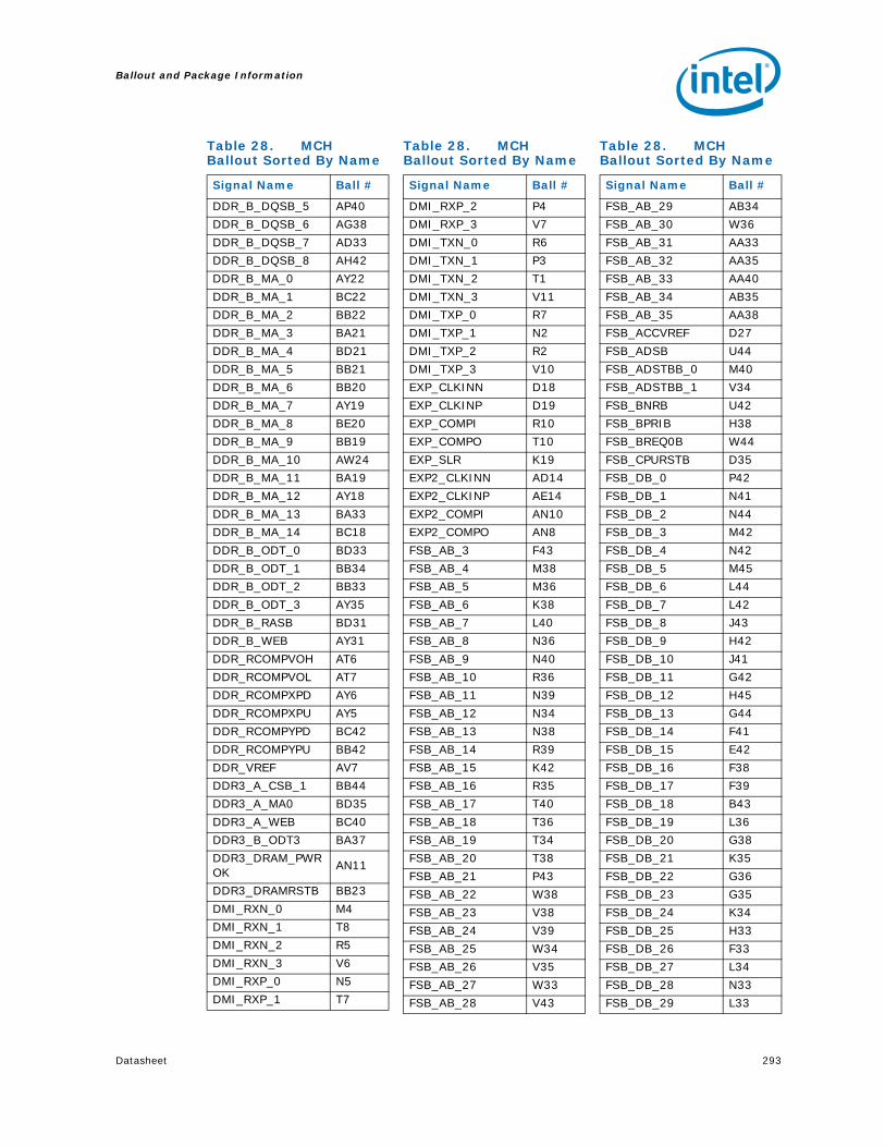
Datasheet 293
Ballout and Package Information
DDR_B_DQSB_5 AP40
DDR_B_DQSB_6 AG38
DDR_B_DQSB_7 AD33
DDR_B_DQSB_8 AH42
DDR_B_MA_0 AY22
DDR_B_MA_1 BC22
DDR_B_MA_2 BB22
DDR_B_MA_3 BA21
DDR_B_MA_4 BD21
DDR_B_MA_5 BB21
DDR_B_MA_6 BB20
DDR_B_MA_7 AY19
DDR_B_MA_8 BE20
DDR_B_MA_9 BB19
DDR_B_MA_10 AW24
DDR_B_MA_11 BA19
DDR_B_MA_12 AY18
DDR_B_MA_13 BA33
DDR_B_MA_14 BC18
DDR_B_ODT_0 BD33
DDR_B_ODT_1 BB34
DDR_B_ODT_2 BB33
DDR_B_ODT_3 AY35
DDR_B_RASB BD31
DDR_B_WEB AY31
DDR_RCOMPVOH AT6
DDR_RCOMPVOL AT7
DDR_RCOMPXPD AY6
DDR_RCOMPXPU AY5
DDR_RCOMPYPD BC42
DDR_RCOMPYPU BB42
DDR_VREF AV7
DDR3_A_CSB_1 BB44
DDR3_A_MA0 BD35
DDR3_A_WEB BC40
DDR3_B_ODT3 BA37
DDR3_DRAM_PWROK
AN11
DDR3_DRAMRSTB BB23
DMI_RXN_0 M4
DMI_RXN_1 T8
DMI_RXN_2 R5
DMI_RXN_3 V6
DMI_RXP_0 N5
DMI_RXP_1 T7
Table 28. MCH Ballout Sorted By Name
Signal Name Ball #
DMI_RXP_2 P4
DMI_RXP_3 V7
DMI_TXN_0 R6
DMI_TXN_1 P3
DMI_TXN_2 T1
DMI_TXN_3 V11
DMI_TXP_0 R7
DMI_TXP_1 N2
DMI_TXP_2 R2
DMI_TXP_3 V10
EXP_CLKINN D18
EXP_CLKINP D19
EXP_COMPI R10
EXP_COMPO T10
EXP_SLR K19
EXP2_CLKINN AD14
EXP2_CLKINP AE14
EXP2_COMPI AN10
EXP2_COMPO AN8
FSB_AB_3 F43
FSB_AB_4 M38
FSB_AB_5 M36
FSB_AB_6 K38
FSB_AB_7 L40
FSB_AB_8 N36
FSB_AB_9 N40
FSB_AB_10 R36
FSB_AB_11 N39
FSB_AB_12 N34
FSB_AB_13 N38
FSB_AB_14 R39
FSB_AB_15 K42
FSB_AB_16 R35
FSB_AB_17 T40
FSB_AB_18 T36
FSB_AB_19 T34
FSB_AB_20 T38
FSB_AB_21 P43
FSB_AB_22 W38
FSB_AB_23 V38
FSB_AB_24 V39
FSB_AB_25 W34
FSB_AB_26 V35
FSB_AB_27 W33
FSB_AB_28 V43
Table 28. MCH Ballout Sorted By Name
Signal Name Ball #
FSB_AB_29 AB34
FSB_AB_30 W36
FSB_AB_31 AA33
FSB_AB_32 AA35
FSB_AB_33 AA40
FSB_AB_34 AB35
FSB_AB_35 AA38
FSB_ACCVREF D27
FSB_ADSB U44
FSB_ADSTBB_0 M40
FSB_ADSTBB_1 V34
FSB_BNRB U42
FSB_BPRIB H38
FSB_BREQ0B W44
FSB_CPURSTB D35
FSB_DB_0 P42
FSB_DB_1 N41
FSB_DB_2 N44
FSB_DB_3 M42
FSB_DB_4 N42
FSB_DB_5 M45
FSB_DB_6 L44
FSB_DB_7 L42
FSB_DB_8 J43
FSB_DB_9 H42
FSB_DB_10 J41
FSB_DB_11 G42
FSB_DB_12 H45
FSB_DB_13 G44
FSB_DB_14 F41
FSB_DB_15 E42
FSB_DB_16 F38
FSB_DB_17 F39
FSB_DB_18 B43
FSB_DB_19 L36
FSB_DB_20 G38
FSB_DB_21 K35
FSB_DB_22 G36
FSB_DB_23 G35
FSB_DB_24 K34
FSB_DB_25 H33
FSB_DB_26 F33
FSB_DB_27 L34
FSB_DB_28 N33
FSB_DB_29 L33
Table 28. MCH Ballout Sorted By Name
Signal Name Ball #

294 Datasheet
Ballout and Package Information
FSB_DB_30 N31
FSB_DB_31 M31
FSB_DB_32 F31
FSB_DB_33 K31
FSB_DB_34 H31
FSB_DB_35 M30
FSB_DB_36 L30
FSB_DB_37 N30
FSB_DB_38 G30
FSB_DB_39 H30
FSB_DB_40 K28
FSB_DB_41 L28
FSB_DB_42 N24
FSB_DB_43 L25
FSB_DB_44 L24
FSB_DB_45 H24
FSB_DB_46 K24
FSB_DB_47 G24
FSB_DB_48 F35
FSB_DB_49 A38
FSB_DB_50 E41
FSB_DB_51 C42
FSB_DB_52 D44
FSB_DB_53 D43
FSB_DB_54 D38
FSB_DB_55 B42
FSB_DB_56 B39
FSB_DB_57 D39
FSB_DB_58 C36
FSB_DB_59 D36
FSB_DB_60 C37
FSB_DB_61 E37
FSB_DB_62 B35
FSB_DB_63 E35
FSB_DBSYB T42
FSB_DEFERB T39
FSB_DINVB_0 L41
FSB_DINVB_1 E40
FSB_DINVB_2 N28
FSB_DINVB_3 B37
FSB_DRDYB U41
FSB_DSTBNB_0 K43
FSB_DSTBNB_1 G34
FSB_DSTBNB_2 M25
FSB_DSTBNB_3 D41
Table 28. MCH Ballout Sorted By Name
Signal Name Ball #
FSB_DSTBPB_0 J44
FSB_DSTBPB_1 H34
FSB_DSTBPB_2 N25
FSB_DSTBPB_3 C40
FSB_DVREF E27
FSB_HITB R42
FSB_HITMB V42
FSB_LOCKB T45
FSB_RCOMP C26
FSB_REQB_0 C44
FSB_REQB_1 G40
FSB_REQB_2 L39
FSB_REQB_3 K36
FSB_REQB_4 H39
FSB_RSB_0 R44
FSB_RSB_1 W41
FSB_RSB_2 R41
FSB_SCOMP D28
FSB_SCOMPB C28
FSB_SWING A28
FSB_TRDYB W40
HPL_CLKINN P30
HPL_CLKINP P28
ICH_SYNCB P16
MTYPE G19
NC BE2
NC BD45
NC BD1
NC B45
NC B1
NC A44
PEG_RXN_0 B15
PEG_RXN_1 C14
PEG_RXN_2 G13
PEG_RXN_3 K13
PEG_RXN_4 M13
PEG_RXN_5 G12
PEG_RXN_6 L12
PEG_RXN_7 H10
PEG_RXN_8 D5
PEG_RXN_9 G6
PEG_RXN_10 C2
PEG_RXN_11 K8
PEG_RXN_12 L10
PEG_RXN_13 M8
Table 28. MCH Ballout Sorted By Name
Signal Name Ball #
PEG_RXN_14 J2
PEG_RXN_15 N10
PEG_RXP_0 A16
PEG_RXP_1 B13
PEG_RXP_2 H13
PEG_RXP_3 L13
PEG_RXP_4 N13
PEG_RXP_5 H12
PEG_RXP_6 K11
PEG_RXP_7 G10
PEG_RXP_8 E6
PEG_RXP_9 F7
PEG_RXP_10 D2
PEG_RXP_11 K7
PEG_RXP_12 M11
PEG_RXP_13 M7
PEG_RXP_14 K3
PEG_RXP_15 N8
PEG_TXN_0 E17
PEG_TXN_1 D14
PEG_TXN_2 D12
PEG_TXN_3 A12
PEG_TXN_4 E11
PEG_TXN_5 C10
PEG_TXN_6 E9
PEG_TXN_7 A8
PEG_TXN_8 C4
PEG_TXN_9 B4
PEG_TXN_10 D3
PEG_TXN_11 E4
PEG_TXN_12 G2
PEG_TXN_13 H4
PEG_TXN_14 K4
PEG_TXN_15 L2
PEG_TXP_0 D16
PEG_TXP_1 E15
PEG_TXP_2 E13
PEG_TXP_3 B11
PEG_TXP_4 D10
PEG_TXP_5 B9
PEG_TXP_6 D8
PEG_TXP_7 B7
PEG_TXP_8 C6
PEG_TXP_9 B3
PEG_TXP_10 F3
Table 28. MCH Ballout Sorted By Name
Signal Name Ball #

Datasheet 295
Ballout and Package Information
PEG_TXP_11 F5
PEG_TXP_12 H1
PEG_TXP_13 J5
PEG_TXP_14 L5
PEG_TXP_15 M1
PEG2_RXN_0 AA13
PEG2_RXN_1 AA11
PEG2_RXN_2 AA7
PEG2_RXN_3 AB12
PEG2_RXN_4 AC10
PEG2_RXN_5 AC7
PEG2_RXN_6 AD12
PEG2_RXN_7 AE11
PEG2_RXN_8 AE6
PEG2_RXN_9 AH13
PEG2_RXN_10 AH10
PEG2_RXN_11 AH6
PEG2_RXN_12 AK13
PEG2_RXN_13 AL10
PEG2_RXN_14 AL7
PEG2_RXN_15 AP11
PEG2_RXP_0 W12
PEG2_RXP_1 AA10
PEG2_RXP_2 AA6
PEG2_RXP_3 AC13
PEG2_RXP_4 AC11
PEG2_RXP_5 AC6
PEG2_RXP_6 AE13
PEG2_RXP_7 AE10
PEG2_RXP_8 AE7
PEG2_RXP_9 AG12
PEG2_RXP_10 AH11
PEG2_RXP_11 AH7
PEG2_RXP_12 AK12
PEG2_RXP_13 AL11
PEG2_RXP_14 AL6
PEG2_RXP_15 AP10
PEG2_TXN_0 AB1
PEG2_TXN_1 AC4
PEG2_TXN_2 AD3
PEG2_TXN_3 AE5
PEG2_TXN_4 AF1
PEG2_TXN_5 AG5
PEG2_TXN_6 AH3
PEG2_TXN_7 AJ5
Table 28. MCH Ballout Sorted By Name
Signal Name Ball #
PEG2_TXN_8 AK1
PEG2_TXN_9 AL5
PEG2_TXN_10 AM3
PEG2_TXN_11 AN5
PEG2_TXN_12 AP1
PEG2_TXN_13 AR5
PEG2_TXN_14 AT3
PEG2_TXN_15 AP6
PEG2_TXP_0 AB3
PEG2_TXP_1 AD4
PEG2_TXP_2 AE2
PEG2_TXP_3 AF4
PEG2_TXP_4 AG2
PEG2_TXP_5 AH4
PEG2_TXP_6 AJ2
PEG2_TXP_7 AK4
PEG2_TXP_8 AL2
PEG2_TXP_9 AM4
PEG2_TXP_10 AN2
PEG2_TXP_11 AP4
PEG2_TXP_12 AR2
PEG2_TXP_13 AT4
PEG2_TXP_14 AU2
PEG2_TXP_15 AP7
PWROK AM19
RSTINB AM18
RSVD L18
RSVD BC2
RSVD AP34
RSVD AP12
RSVD AN31
RSVD AN30
RSVD AN25
RSVD AN13
RSVD AN12
RSVD AM32
RSVD AM25
RSVD AM14
RSVD AL28
RSVD AH28
RSVD AG32
RSVD AG28
RSVD AD32
RSVD W32
RSVD V32
Table 28. MCH Ballout Sorted By Name
Signal Name Ball #
RSVD V12
RSVD T33
RSVD T12
RSVD R33
RSVD R22
RSVD R19
RSVD P21
RSVD N21
RSVD N18
RSVD N12
RSVD N11
RSVD M16
RSVD L19
RSVD K22
RSVD K21
RSVD H21
RSVD G22
RSVD F19
RSVD B19
RSVD_G15 G15
RSVD_H15 H15
RSVD_M19 M19
RSVD_P19 P19
TCEN G21
TEST0 BE45
TEST1 BE1
TEST2 A2
TEST3 A45
VCC AH26
VCC AH24
VCC AH22
VCC AH20
VCC AH19
VCC AH18
VCC AH17
VCC AG27
VCC AG25
VCC AG23
VCC AG21
VCC AG19
VCC AG18
VCC AG17
VCC AG15
VCC AF28
VCC AF26
Table 28. MCH Ballout Sorted By Name
Signal Name Ball #

296 Datasheet
Ballout and Package Information
VCC AF24
VCC AF22
VCC AF20
VCC AF18
VCC AF17
VCC AE28
VCC AE27
VCC AE25
VCC AE23
VCC AE21
VCC AE19
VCC AE18
VCC AE17
VCC AD28
VCC AD26
VCC AD24
VCC AD22
VCC AD20
VCC AD18
VCC AD17
VCC AC28
VCC AC27
VCC AC25
VCC AC23
VCC AC21
VCC AC19
VCC AC18
VCC AC17
VCC AB28
VCC AB26
VCC AB24
VCC AB22
VCC AB20
VCC AB18
VCC AB17
VCC AB15
VCC AA28
VCC AA27
VCC AA25
VCC AA23
VCC AA21
VCC AA19
VCC AA18
VCC AA17
VCC Y28
Table 28. MCH Ballout Sorted By Name
Signal Name Ball #
VCC Y26
VCC Y24
VCC Y22
VCC Y20
VCC Y18
VCC Y17
VCC W28
VCC W27
VCC W25
VCC W23
VCC W21
VCC W19
VCC W18
VCC W17
VCC V28
VCC V26
VCC V24
VCC V22
VCC V20
VCC V18
VCC V17
VCC U28
VCC U27
VCC U26
VCC U25
VCC U24
VCC U23
VCC U22
VCC U21
VCC U20
VCC U19
VCC U18
VCC U17
VCC R18
VCC R16
VCC_B25 B25
VCC_C18 C18
VCC_CKDDR BE44
VCC_CKDDR BE43
VCC_CKDDR BD44
VCC_CKDDR BD43
VCC_CKDDR BC45
VCC_CKDDR BC44
VCC_CL V31
VCC_CL AM30
Table 28. MCH Ballout Sorted By Name
Signal Name Ball #
VCC_CL AM23
VCC_CL AM22
VCC_CL AL30
VCC_CL AL27
VCC_CL AL25
VCC_CL AL24
VCC_CL AL23
VCC_CL AL22
VCC_CL AL21
VCC_CL AL19
VCC_CL AL18
VCC_CL AL16
VCC_CL AK31
VCC_CL AJ29
VCC_CL AJ28
VCC_CL AJ27
VCC_CL AJ26
VCC_CL AJ25
VCC_CL AJ24
VCC_CL AJ23
VCC_CL AJ22
VCC_CL AJ21
VCC_CL AJ20
VCC_CL AJ19
VCC_CL AJ18
VCC_CL AJ17
VCC_CL AH31
VCC_CL AH29
VCC_CL AH15
VCC_CL AH14
VCC_CL AG31
VCC_CL AG29
VCC_CL AF29
VCC_CL AE31
VCC_CL AE29
VCC_CL AD31
VCC_CL AD29
VCC_CL AC31
VCC_CL AC29
VCC_CL AB31
VCC_CL AB29
VCC_CL AA31
VCC_CL AA29
VCC_CL Y29
VCC_CL W29
Table 28. MCH Ballout Sorted By Name
Signal Name Ball #

Datasheet 297
Ballout and Package Information
VCC_CL V29
VCC_DDR BE40
VCC_DDR BE36
VCC_DDR BE32
VCC_DDR BE28
VCC_DDR BE24
VCC_DDR BE22
VCC_DDR BC38
VCC_DDR BC34
VCC_DDR BC30
VCC_DDR BC26
VCC_DDR BC23
VCC_DDR BC20
VCC_DDR AY45
VCC_DDR AY23
VCC_E25 E25
VCC_EXP AD11
VCC_EXP AD10
VCC_EXP AD8
VCC_EXP AD7
VCC_EXP AB11
VCC_EXP AB10
VCC_EXP AB8
VCC_EXP AB7
VCC_EXP AB6
VCC_EXP AB4
VCC_EXP AA5
VCC_EXP AA4
VCC_EXP AA2
VCC_EXP Y4
VCC_EXP Y3
VCC_EXP Y1
VCC_EXP W11
VCC_EXP W10
VCC_EXP W8
VCC_EXP W7
VCC_EXP W5
VCC_EXP W4
VCC_EXP W2
VCC_EXP V4
VCC_EXP V3
VCC_EXP V1
VCC_EXP U5
VCC_EXP U4
VCC_EXP U2
Table 28. MCH Ballout Sorted By Name
Signal Name Ball #
VCC_EXP T4
VCC_EXP T3
VCC_EXT_PLL AB13
VCC_N15 N15
VCC3_3 A23
VCC3_3_G16 G16
VCC3_3_L16 L16
VCCA_EXP D20
VCCA_EXP2 AU5
VCCA_HPL D26
VCCA_HPL D25
VCCA_MPL B27
VCCAPLL_EXP A20
VCCAPLL_EXP2 AR10
VCCAUX U29
VCCAUX T31
VCCAUX R30
VCCAUX R28
VCCAUX R27
VCCAUX R25
VCCAUX R24
VCCAUX R23
VCCR_EXP AP3
VCCR_EXP AK3
VCCR_EXP AF3
VCCR_EXP AE15
VCCR_EXP AD15
VCCR_EXP AC15
VCCR_EXP AC3
VCCR_EXP AB14
VCCR_EXP AA15
VCCR_EXP AA14
VCCR_EXP W15
VCCR_EXP V15
VCCR_EXP V14
VCCR_EXP T15
VCCR_EXP T14
VCCR_EXP M3
VCCR_EXP H3
VCCR_EXP C16
VCCR_EXP C12
VCCR_EXP C8
VSS B2
VSS BE38
VSS BE34
Table 28. MCH Ballout Sorted By Name
Signal Name Ball #
VSS BE30
VSS BE26
VSS BE23
VSS BE18
VSS BE14
VSS BE10
VSS BE6
VSS BE3
VSS BD2
VSS BC43
VSS BC16
VSS BC12
VSS BC8
VSS BC3
VSS BC1
VSS BB2
VSS AY36
VSS AY33
VSS AY10
VSS AW40
VSS AW35
VSS AW31
VSS AW28
VSS AW27
VSS AW21
VSS AW18
VSS AW15
VSS AW7
VSS AW4
VSS AV45
VSS AV43
VSS AV34
VSS AV28
VSS AV24
VSS AV23
VSS AV22
VSS AV18
VSS AV13
VSS AV12
VSS AV11
VSS AV10
VSS AV6
VSS AV4
VSS AV3
VSS AV1
Table 28. MCH Ballout Sorted By Name
Signal Name Ball #

298 Datasheet
Ballout and Package Information
VSS AU3
VSS AT45
VSS AT39
VSS AT30
VSS AT28
VSS AT24
VSS AT23
VSS AT16
VSS AT8
VSS AT1
VSS AR39
VSS AR38
VSS AR35
VSS AR30
VSS AR27
VSS AR23
VSS AR22
VSS AR21
VSS AR19
VSS AR15
VSS AR8
VSS AR7
VSS AR6
VSS AR4
VSS AP43
VSS AP38
VSS AP33
VSS AP30
VSS AP25
VSS AP23
VSS AP22
VSS AP18
VSS AP13
VSS AP8
VSS AN38
VSS AN34
VSS AN23
VSS AN7
VSS AN6
VSS AN4
VSS AM45
VSS AM24
VSS AM21
VSS AM16
VSS AM1
Table 28. MCH Ballout Sorted By Name
Signal Name Ball #
VSS AL39
VSS AL35
VSS AL12
VSS AL8
VSS AL4
VSS AK43
VSS AK40
VSS AK36
VSS AK32
VSS AK11
VSS AK10
VSS AK8
VSS AK7
VSS AK6
VSS AJ41
VSS AJ4
VSS AH45
VSS AH40
VSS AH39
VSS AH38
VSS AH35
VSS AH32
VSS AH27
VSS AH25
VSS AH23
VSS AH21
VSS AH12
VSS AH8
VSS AH1
VSS AG36
VSS AG34
VSS AG26
VSS AG24
VSS AG22
VSS AG20
VSS AG13
VSS AG10
VSS AG8
VSS AG7
VSS AG6
VSS AG4
VSS AF43
VSS AF27
VSS AF25
VSS AF23
Table 28. MCH Ballout Sorted By Name
Signal Name Ball #
VSS AF21
VSS AF19
VSS AE36
VSS AE32
VSS AE26
VSS AE24
VSS AE22
VSS AE20
VSS AE12
VSS AE8
VSS AE4
VSS AD45
VSS AD38
VSS AD34
VSS AD27
VSS AD25
VSS AD23
VSS AD21
VSS AD19
VSS AD13
VSS AD6
VSS AD1
VSS AC43
VSS AC38
VSS AC35
VSS AC32
VSS AC26
VSS AC24
VSS AC22
VSS AC20
VSS AC14
VSS AC12
VSS AC8
VSS AC1
VSS AB45
VSS AB36
VSS AB33
VSS AB27
VSS AB25
VSS AB23
VSS AB21
VSS AB19
VSS AA39
VSS AA36
VSS AA34
Table 28. MCH Ballout Sorted By Name
Signal Name Ball #

Datasheet 299
Ballout and Package Information
VSS AA32
VSS AA26
VSS AA24
VSS AA22
VSS AA20
VSS AA12
VSS AA8
VSS Y43
VSS Y27
VSS Y25
VSS Y23
VSS Y21
VSS Y19
VSS W39
VSS W35
VSS W26
VSS W24
VSS W22
VSS W20
VSS W14
VSS W13
VSS W6
VSS V45
VSS V40
VSS V36
VSS V33
VSS V27
VSS V25
VSS V23
VSS V21
VSS V19
VSS V13
VSS V8
VSS T43
VSS T35
VSS T32
VSS T13
VSS T11
VSS T6
VSS R40
VSS R38
VSS R34
VSS R21
VSS R13
VSS R12
Table 28. MCH Ballout Sorted By Name
Signal Name Ball #
VSS R11
VSS R8
VSS R4
VSS P45
VSS P32
VSS P27
VSS P25
VSS P24
VSS P23
VSS P22
VSS P18
VSS P14
VSS P1
VSS N35
VSS N27
VSS N23
VSS N22
VSS N19
VSS N16
VSS N7
VSS N6
VSS N4
VSS M43
VSS M39
VSS M35
VSS M34
VSS M33
VSS M28
VSS M24
VSS M23
VSS M18
VSS M12
VSS M10
VSS M6
VSS L38
VSS L35
VSS L31
VSS L23
VSS L21
VSS L15
VSS L11
VSS L8
VSS L7
VSS L6
VSS L4
Table 28. MCH Ballout Sorted By Name
Signal Name Ball #
VSS K45
VSS K40
VSS K39
VSS K33
VSS K30
VSS K23
VSS K18
VSS K15
VSS K12
VSS K10
VSS K6
VSS K1
VSS J3
VSS H43
VSS H40
VSS H36
VSS H35
VSS H23
VSS H22
VSS H19
VSS H18
VSS H11
VSS H8
VSS H7
VSS H6
VSS G39
VSS G33
VSS G31
VSS G23
VSS G18
VSS G11
VSS G8
VSS G7
VSS G4
VSS F45
VSS F40
VSS F36
VSS F34
VSS F24
VSS F23
VSS F16
VSS F15
VSS F13
VSS F12
VSS F11
Table 28. MCH Ballout Sorted By Name
Signal Name Ball #

300 Datasheet
Ballout and Package Information
NOTE: See list of notes at beginning of chapter.
VSS F10
VSS F8
VSS F6
VSS F1
VSS E21
VSS E19
VSS E5
VSS D42
VSS D34
VSS D29
VSS D23
VSS D17
VSS D15
VSS D13
VSS D11
VSS D7
VSS D4
VSS C45
VSS C43
VSS C38
VSS C34
VSS C30
VSS C22
VSS C20
VSS C9
VSS C3
VSS C1
VSS B44
VSS B29
VSS A43
VSS A40
VSS A36
VSS A34
VSS A26
VSS A22
VSS A18
VSS A14
VSS A10
VSS A6
VSS A3
VSS_A24 A24
VSS_AW2 AW2
VSS_AY1 AY1
VSS_AY3 AY3
VSS_B17 B17
Table 28. MCH Ballout Sorted By Name
Signal Name Ball #
VSS_B21 B21
VSS_BA4 BA4
VSS_BA5 BA5
VSS_BB3 BB3
VSS_C23 C23
VSS_C24 C24
VSS_D21 D21
VSS_D22 D22
VSS_D24 D24
VSS_F22 F22
VSS_H16 H16
VSS_K16 K16
VSS_M15 M15
VSS_W31 W31
VTT_FSB M27
VTT_FSB L27
VTT_FSB K27
VTT_FSB K25
VTT_FSB H28
VTT_FSB H27
VTT_FSB H25
VTT_FSB G28
VTT_FSB G27
VTT_FSB G25
VTT_FSB F30
VTT_FSB F28
VTT_FSB F27
VTT_FSB F25
VTT_FSB E33
VTT_FSB E31
VTT_FSB E29
VTT_FSB D33
VTT_FSB D32
VTT_FSB D31
VTT_FSB D30
VTT_FSB C32
VTT_FSB B33
VTT_FSB B31
VTT_FSB A32
VTT_FSB A30
XORTEST L22
Table 28. MCH Ballout Sorted By Name
Signal Name Ball #
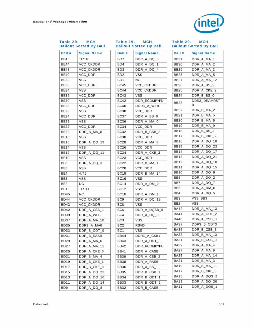
Datasheet 301
Ballout and Package Information
Table 29. MCH Ballout Sorted By Ball
Ball # Signal Name
BE45 TEST0
BE44 VCC_CKDDR
BE43 VCC_CKDDR
BE40 VCC_DDR
BE38 VSS
BE36 VCC_DDR
BE34 VSS
BE32 VCC_DDR
BE30 VSS
BE28 VCC_DDR
BE26 VSS
BE24 VCC_DDR
BE23 VSS
BE22 VCC_DDR
BE20 DDR_B_MA_8
BE18 VSS
BE16 DDR_A_DQ_19
BE14 VSS
BE12 DDR_A_DQ_11
BE10 VSS
BE8 DDR_A_DQ_3
BE6 VSS
BE4 4.75
BE3 VSS
BE2 NC
BE1 TEST1
BD45 NC
BD44 VCC_CKDDR
BD43 VCC_CKDDR
BD42 DDR_A_CSB_1
BD39 DDR_A_WEB
BD37 DDR_A_MA_10
BD35 DDR3_A_MA0
BD33 DDR_B_ODT_0
BD31 DDR_B_RASB
BD29 DDR_A_MA_6
BD27 DDR_A_MA_11
BD25 DDR_A_CKE_0
BD21 DDR_B_MA_4
BD19 DDR_B_CKE_1
BD17 DDR_B_CKE_0
BD15 DDR_A_DQ_22
BD13 DDR_A_DQ_16
BD11 DDR_A_DQ_14
BD9 DDR_A_DQ_8
BD7 DDR_A_DQ_6
BD4 DDR_A_DQ_1
BD3 DDR_A_DQ_4
BD2 VSS
BD1 NC
BC45 VCC_CKDDR
BC44 VCC_CKDDR
BC43 VSS
BC42 DDR_RCOMPYPD
BC40 DDR3_A_WEB
BC38 VCC_DDR
BC37 DDR_A_BS_0
BC36 DDR_A_MA_0
BC34 VCC_DDR
BC32 DDR_B_CSB_2
BC30 VCC_DDR
BC28 DDR_A_MA_8
BC26 VCC_DDR
BC24 DDR_A_CKE_3
BC23 VCC_DDR
BC22 DDR_B_MA_1
BC20 VCC_DDR
BC18 DDR_B_MA_14
BC16 VSS
BC14 DDR_A_DM_2
BC12 VSS
BC10 DDR_A_DM_1
BC9 DDR_A_DQ_13
BC8 VSS
BC6 DDR_A_DQSB_0
BC4 DDR_A_DQ_0
BC3 VSS
BC2 RSVD
BC1 VSS
BB44 DDR3_A_CSB1
BB43 DDR_A_ODT_0
BB42 DDR_RCOMPYPU
BB41 DDR_A_CASB
BB39 DDR_A_CSB_2
BB38 DDR_A_RASB
BB36 DDR_A_BS_1
BB35 DDR_B_CSB_1
BB34 DDR_B_ODT_1
BB33 DDR_B_ODT_2
BB32 DDR_B_CASB
Table 29. MCH Ballout Sorted By Ball
Ball # Signal Name
BB31 DDR_A_MA_1
BB30 DDR_A_MA_2
BB29 DDR_A_MA_3
BB28 DDR_A_MA_5
BB27 DDR_A_MA_12
BB26 DDR_A_BS_2
BB25 DDR_A_CKE_2
BB24 DDR_B_BS_0
BB23DDR3_DRAMRSTB
BB22 DDR_B_MA_2
BB21 DDR_B_MA_5
BB20 DDR_B_MA_6
BB19 DDR_B_MA_9
BB18 DDR_B_BS_2
BB17 DDR_B_CKE_2
BB16 DDR_A_DQ_18
BB15 DDR_A_DQ_23
BB14 DDR_A_DQ_17
BB13 DDR_A_DQ_21
BB12 DDR_A_DQ_10
BB11 DDR_A_DQ_15
BB10 DDR_A_DQ_9
BB8 DDR_A_DQ_2
BB7 DDR_A_DQ_7
BB5 DDR_A_DM_0
BB4 DDR_A_DQ_5
BB3 VSS_BB3
BB2 VSS
BA42 DDR_A_MA_13
BA41 DDR_A_ODT_2
BA40 DDR_A_CSB_0
BA37 DDR3_B_ODT3
BA35 DDR_B_CSB_3
BA33 DDR_B_MA_13
BA31 DDR_B_CSB_0
BA29 DDR_A_MA_4
BA27 DDR_A_MA_9
BA25 DDR_A_MA_14
BA21 DDR_B_MA_3
BA19 DDR_B_MA_11
BA17 DDR_B_CKE_3
BA15 DDR_A_DQS_2
BA13 DDR_A_DQ_20
BA11 DDR_A_DQS_1
Table 29. MCH Ballout Sorted By Ball
Ball # Signal Name
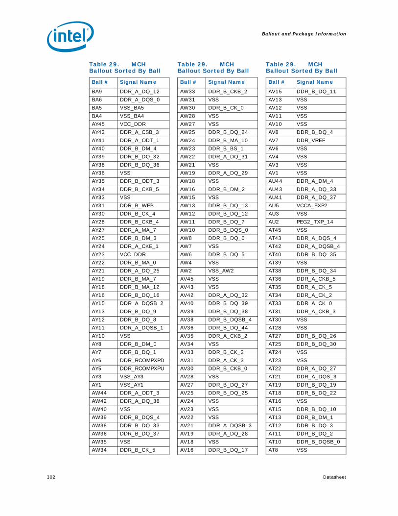
302 Datasheet
Ballout and Package Information
BA9 DDR_A_DQ_12
BA6 DDR_A_DQS_0
BA5 VSS_BA5
BA4 VSS_BA4
AY45 VCC_DDR
AY43 DDR_A_CSB_3
AY41 DDR_A_ODT_1
AY40 DDR_B_DM_4
AY39 DDR_B_DQ_32
AY38 DDR_B_DQ_36
AY36 VSS
AY35 DDR_B_ODT_3
AY34 DDR_B_CKB_5
AY33 VSS
AY31 DDR_B_WEB
AY30 DDR_B_CK_4
AY28 DDR_B_CKB_4
AY27 DDR_A_MA_7
AY25 DDR_B_DM_3
AY24 DDR_A_CKE_1
AY23 VCC_DDR
AY22 DDR_B_MA_0
AY21 DDR_A_DQ_25
AY19 DDR_B_MA_7
AY18 DDR_B_MA_12
AY16 DDR_B_DQ_16
AY15 DDR_A_DQSB_2
AY13 DDR_B_DQ_9
AY12 DDR_B_DQ_8
AY11 DDR_A_DQSB_1
AY10 VSS
AY8 DDR_B_DM_0
AY7 DDR_B_DQ_1
AY6 DDR_RCOMPXPD
AY5 DDR_RCOMPXPU
AY3 VSS_AY3
AY1 VSS_AY1
AW44 DDR_A_ODT_3
AW42 DDR_A_DQ_36
AW40 VSS
AW39 DDR_B_DQS_4
AW38 DDR_B_DQ_33
AW36 DDR_B_DQ_37
AW35 VSS
AW34 DDR_B_CK_5
Table 29. MCH Ballout Sorted By Ball
Ball # Signal Name
AW33 DDR_B_CKB_2
AW31 VSS
AW30 DDR_B_CK_0
AW28 VSS
AW27 VSS
AW25 DDR_B_DQ_24
AW24 DDR_B_MA_10
AW23 DDR_B_BS_1
AW22 DDR_A_DQ_31
AW21 VSS
AW19 DDR_A_DQ_29
AW18 VSS
AW16 DDR_B_DM_2
AW15 VSS
AW13 DDR_B_DQ_13
AW12 DDR_B_DQ_12
AW11 DDR_B_DQ_7
AW10 DDR_B_DQS_0
AW8 DDR_B_DQ_0
AW7 VSS
AW6 DDR_B_DQ_5
AW4 VSS
AW2 VSS_AW2
AV45 VSS
AV43 VSS
AV42 DDR_A_DQ_32
AV40 DDR_B_DQ_39
AV39 DDR_B_DQ_38
AV38 DDR_B_DQSB_4
AV36 DDR_B_DQ_44
AV35 DDR_A_CKB_2
AV34 VSS
AV33 DDR_B_CK_2
AV31 DDR_A_CK_3
AV30 DDR_B_CKB_0
AV28 VSS
AV27 DDR_B_DQ_27
AV25 DDR_B_DQ_25
AV24 VSS
AV23 VSS
AV22 VSS
AV21 DDR_A_DQSB_3
AV19 DDR_A_DQ_28
AV18 VSS
AV16 DDR_B_DQ_17
Table 29. MCH Ballout Sorted By Ball
Ball # Signal Name
AV15 DDR_B_DQ_11
AV13 VSS
AV12 VSS
AV11 VSS
AV10 VSS
AV8 DDR_B_DQ_4
AV7 DDR_VREF
AV6 VSS
AV4 VSS
AV3 VSS
AV1 VSS
AU44 DDR_A_DM_4
AU43 DDR_A_DQ_33
AU41 DDR_A_DQ_37
AU5 VCCA_EXP2
AU3 VSS
AU2 PEG2_TXP_14
AT45 VSS
AT43 DDR_A_DQS_4
AT42 DDR_A_DQSB_4
AT40 DDR_B_DQ_35
AT39 VSS
AT38 DDR_B_DQ_34
AT36 DDR_A_CKB_5
AT35 DDR_A_CK_5
AT34 DDR_A_CK_2
AT33 DDR_A_CK_0
AT31 DDR_A_CKB_3
AT30 VSS
AT28 VSS
AT27 DDR_B_DQ_26
AT25 DDR_B_DQ_30
AT24 VSS
AT23 VSS
AT22 DDR_A_DQ_27
AT21 DDR_A_DQS_3
AT19 DDR_B_DQ_19
AT18 DDR_B_DQ_22
AT16 VSS
AT15 DDR_B_DQ_10
AT13 DDR_B_DM_1
AT12 DDR_B_DQ_3
AT11 DDR_B_DQ_2
AT10 DDR_B_DQSB_0
AT8 VSS
Table 29. MCH Ballout Sorted By Ball
Ball # Signal Name
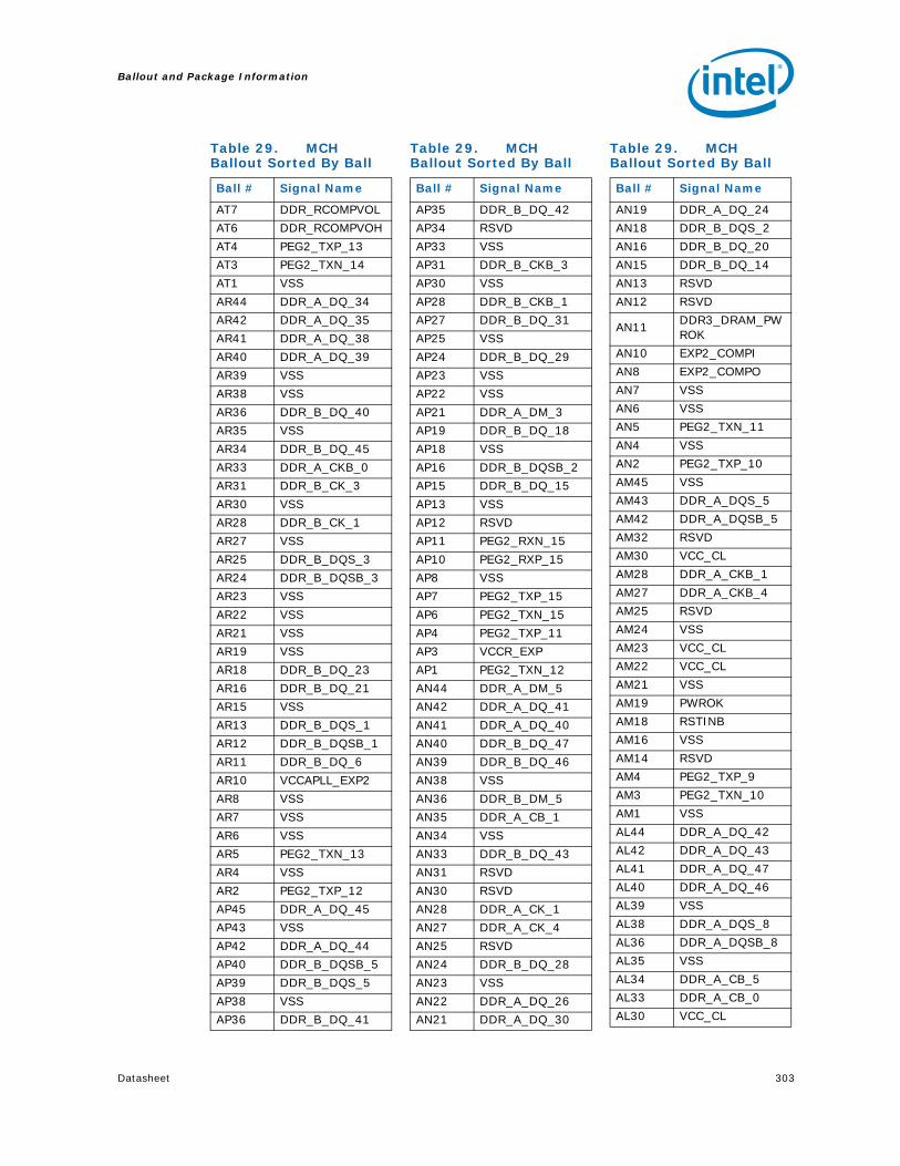
Datasheet 303
Ballout and Package Information
AT7 DDR_RCOMPVOL
AT6 DDR_RCOMPVOH
AT4 PEG2_TXP_13
AT3 PEG2_TXN_14
AT1 VSS
AR44 DDR_A_DQ_34
AR42 DDR_A_DQ_35
AR41 DDR_A_DQ_38
AR40 DDR_A_DQ_39
AR39 VSS
AR38 VSS
AR36 DDR_B_DQ_40
AR35 VSS
AR34 DDR_B_DQ_45
AR33 DDR_A_CKB_0
AR31 DDR_B_CK_3
AR30 VSS
AR28 DDR_B_CK_1
AR27 VSS
AR25 DDR_B_DQS_3
AR24 DDR_B_DQSB_3
AR23 VSS
AR22 VSS
AR21 VSS
AR19 VSS
AR18 DDR_B_DQ_23
AR16 DDR_B_DQ_21
AR15 VSS
AR13 DDR_B_DQS_1
AR12 DDR_B_DQSB_1
AR11 DDR_B_DQ_6
AR10 VCCAPLL_EXP2
AR8 VSS
AR7 VSS
AR6 VSS
AR5 PEG2_TXN_13
AR4 VSS
AR2 PEG2_TXP_12
AP45 DDR_A_DQ_45
AP43 VSS
AP42 DDR_A_DQ_44
AP40 DDR_B_DQSB_5
AP39 DDR_B_DQS_5
AP38 VSS
AP36 DDR_B_DQ_41
Table 29. MCH Ballout Sorted By Ball
Ball # Signal Name
AP35 DDR_B_DQ_42
AP34 RSVD
AP33 VSS
AP31 DDR_B_CKB_3
AP30 VSS
AP28 DDR_B_CKB_1
AP27 DDR_B_DQ_31
AP25 VSS
AP24 DDR_B_DQ_29
AP23 VSS
AP22 VSS
AP21 DDR_A_DM_3
AP19 DDR_B_DQ_18
AP18 VSS
AP16 DDR_B_DQSB_2
AP15 DDR_B_DQ_15
AP13 VSS
AP12 RSVD
AP11 PEG2_RXN_15
AP10 PEG2_RXP_15
AP8 VSS
AP7 PEG2_TXP_15
AP6 PEG2_TXN_15
AP4 PEG2_TXP_11
AP3 VCCR_EXP
AP1 PEG2_TXN_12
AN44 DDR_A_DM_5
AN42 DDR_A_DQ_41
AN41 DDR_A_DQ_40
AN40 DDR_B_DQ_47
AN39 DDR_B_DQ_46
AN38 VSS
AN36 DDR_B_DM_5
AN35 DDR_A_CB_1
AN34 VSS
AN33 DDR_B_DQ_43
AN31 RSVD
AN30 RSVD
AN28 DDR_A_CK_1
AN27 DDR_A_CK_4
AN25 RSVD
AN24 DDR_B_DQ_28
AN23 VSS
AN22 DDR_A_DQ_26
AN21 DDR_A_DQ_30
Table 29. MCH Ballout Sorted By Ball
Ball # Signal Name
AN19 DDR_A_DQ_24
AN18 DDR_B_DQS_2
AN16 DDR_B_DQ_20
AN15 DDR_B_DQ_14
AN13 RSVD
AN12 RSVD
AN11DDR3_DRAM_PWROK
AN10 EXP2_COMPI
AN8 EXP2_COMPO
AN7 VSS
AN6 VSS
AN5 PEG2_TXN_11
AN4 VSS
AN2 PEG2_TXP_10
AM45 VSS
AM43 DDR_A_DQS_5
AM42 DDR_A_DQSB_5
AM32 RSVD
AM30 VCC_CL
AM28 DDR_A_CKB_1
AM27 DDR_A_CKB_4
AM25 RSVD
AM24 VSS
AM23 VCC_CL
AM22 VCC_CL
AM21 VSS
AM19 PWROK
AM18 RSTINB
AM16 VSS
AM14 RSVD
AM4 PEG2_TXP_9
AM3 PEG2_TXN_10
AM1 VSS
AL44 DDR_A_DQ_42
AL42 DDR_A_DQ_43
AL41 DDR_A_DQ_47
AL40 DDR_A_DQ_46
AL39 VSS
AL38 DDR_A_DQS_8
AL36 DDR_A_DQSB_8
AL35 VSS
AL34 DDR_A_CB_5
AL33 DDR_A_CB_0
AL30 VCC_CL
Table 29. MCH Ballout Sorted By Ball
Ball # Signal Name

304 Datasheet
Ballout and Package Information
AL28 RSVD
AL27 VCC_CL
AL25 VCC_CL
AL24 VCC_CL
AL23 VCC_CL
AL22 VCC_CL
AL21 VCC_CL
AL19 VCC_CL
AL18 VCC_CL
AL16 VCC_CL
AL13 CL_PWROK
AL12 VSS
AL11 PEG2_RXP_13
AL10 PEG2_RXN_13
AL8 VSS
AL7 PEG2_RXN_14
AL6 PEG2_RXP_14
AL5 PEG2_TXN_9
AL4 VSS
AL2 PEG2_TXP_8
AK45 DDR_B_CB_0
AK43 VSS
AK42 DDR_B_CB_5
AK40 VSS
AK39 DDR_A_CB_7
AK38 DDR_A_CB_2
AK36 VSS
AK35 DDR_A_CB_3
AK34 DDR_A_CB_6
AK33 DDR_A_CB_4
AK32 VSS
AK31 VCC_CL
AK15 CL_DATA
AK14 CL_CLK
AK13 PEG2_RXN_12
AK12 PEG2_RXP_12
AK11 VSS
AK10 VSS
AK8 VSS
AK7 VSS
AK6 VSS
AK4 PEG2_TXP_7
AK3 VCCR_EXP
AK1 PEG2_TXN_8
AJ44 DDR_B_CB_1
Table 29. MCH Ballout Sorted By Ball
Ball # Signal Name
AJ42 DDR_B_CB_4
AJ41 VSS
AJ29 VCC_CL
AJ28 VCC_CL
AJ27 VCC_CL
AJ26 VCC_CL
AJ25 VCC_CL
AJ24 VCC_CL
AJ23 VCC_CL
AJ22 VCC_CL
AJ21 VCC_CL
AJ20 VCC_CL
AJ19 VCC_CL
AJ18 VCC_CL
AJ17 VCC_CL
AJ5 PEG2_TXN_7
AJ4 VSS
AJ2 PEG2_TXP_6
AH45 VSS
AH43 DDR_B_DQS_8
AH42 DDR_B_DQSB_8
AH40 VSS
AH39 VSS
AH38 VSS
AH36 DDR_B_DQ_53
AH35 VSS
AH34 DDR_B_DQ_48
AH33 DDR_B_DQ_52
AH32 VSS
AH31 VCC_CL
AH29 VCC_CL
AH28 RSVD
AH27 VSS
AH26 VCC
AH25 VSS
AH24 VCC
AH23 VSS
AH22 VCC
AH21 VSS
AH20 VCC
AH19 VCC
AH18 VCC
AH17 VCC
AH15 VCC_CL
AH14 VCC_CL
Table 29. MCH Ballout Sorted By Ball
Ball # Signal Name
AH13 PEG2_RXN_9
AH12 VSS
AH11 PEG2_RXP_10
AH10 PEG2_RXN_10
AH8 VSS
AH7 PEG2_RXP_11
AH6 PEG2_RXN_11
AH4 PEG2_TXP_5
AH3 PEG2_TXN_6
AH1 VSS
AG44 DDR_B_CB_7
AG42 DDR_B_CB_2
AG41 DDR_B_CB_6
AG40 DDR_B_CB_3
AG39 DDR_B_DQS_6
AG38 DDR_B_DQSB_6
AG36 VSS
AG35 DDR_B_DM_6
AG34 VSS
AG33 DDR_B_DQ_49
AG32 RSVD
AG31 VCC_CL
AG29 VCC_CL
AG28 RSVD
AG27 VCC
AG26 VSS
AG25 VCC
AG24 VSS
AG23 VCC
AG22 VSS
AG21 VCC
AG20 VSS
AG19 VCC
AG18 VCC
AG17 VCC
AG15 VCC
AG14 CL_VREF
AG13 VSS
AG12 PEG2_RXP_9
AG11 CL_RSTB
AG10 VSS
AG8 VSS
AG7 VSS
AG6 VSS
AG5 PEG2_TXN_5
Table 29. MCH Ballout Sorted By Ball
Ball # Signal Name

Datasheet 305
Ballout and Package Information
AG4 VSS
AG2 PEG2_TXP_4
AF45 DDR_A_DQ_53
AF43 VSS
AF42 DDR_A_DQ_52
AF29 VCC_CL
AF28 VCC
AF27 VSS
AF26 VCC
AF25 VSS
AF24 VCC
AF23 VSS
AF22 VCC
AF21 VSS
AF20 VCC
AF19 VSS
AF18 VCC
AF17 VCC
AF4 PEG2_TXP_3
AF3 VCCR_EXP
AF1 PEG2_TXN_4
AE44 DDR_A_DM_6
AE42 DDR_A_DQ_49
AE41 DDR_A_DQ_48
AE40 DDR_B_DQ_54
AE39 DDR_B_DQ_50
AE38 DDR_B_DQ_51
AE36 VSS
AE35 DDR_B_DQ_60
AE34 DDR_B_DQ_61
AE33 DDR_B_DQ_55
AE32 VSS
AE31 VCC_CL
AE29 VCC_CL
AE28 VCC
AE27 VCC
AE26 VSS
AE25 VCC
AE24 VSS
AE23 VCC
AE22 VSS
AE21 VCC
AE20 VSS
AE19 VCC
AE18 VCC
Table 29. MCH Ballout Sorted By Ball
Ball # Signal Name
AE17 VCC
AE15 VCCR_EXP
AE14 EXP2_CLKINP
AE13 PEG2_RXP_6
AE12 VSS
AE11 PEG2_RXN_7
AE10 PEG2_RXP_7
AE8 VSS
AE7 PEG2_RXP_8
AE6 PEG2_RXN_8
AE5 PEG2_TXN_3
AE4 VSS
AE2 PEG2_TXP_2
AD45 VSS
AD43 DDR_A_DQS_6
AD42 DDR_A_DQSB_6
AD40 DDR_A_DQ_54
AD39 DDR_B_DQ_56
AD38 VSS
AD36 DDR_B_DQ_57
AD35 DDR_B_DM_7
AD34 VSS
AD33 DDR_B_DQSB_7
AD32 RSVD
AD31 VCC_CL
AD29 VCC_CL
AD28 VCC
AD27 VSS
AD26 VCC
AD25 VSS
AD24 VCC
AD23 VSS
AD22 VCC
AD21 VSS
AD20 VCC
AD19 VSS
AD18 VCC
AD17 VCC
AD15 VCCR_EXP
AD14 EXP2_CLKINN
AD13 VSS
AD12 PEG2_RXN_6
AD11 VCC_EXP
AD10 VCC_EXP
AD8 VCC_EXP
Table 29. MCH Ballout Sorted By Ball
Ball # Signal Name
AD7 VCC_EXP
AD6 VSS
AD4 PEG2_TXP_1
AD3 PEG2_TXN_2
AD1 VSS
AC45 DDR_A_DQ_51
AC43 VSS
AC42 DDR_A_DQ_50
AC40 DDR_A_DQ_60
AC39 DDR_A_DQ_55
AC38 VSS
AC36 DDR_B_DQ_62
AC35 VSS
AC34 DDR_B_DQ_63
AC33 DDR_B_DQS_7
AC32 VSS
AC31 VCC_CL
AC29 VCC_CL
AC28 VCC
AC27 VCC
AC26 VSS
AC25 VCC
AC24 VSS
AC23 VCC
AC22 VSS
AC21 VCC
AC20 VSS
AC19 VCC
AC18 VCC
AC17 VCC
AC15 VCCR_EXP
AC14 VSS
AC13 PEG2_RXP_3
AC12 VSS
AC11 PEG2_RXP_4
AC10 PEG2_RXN_4
AC8 VSS
AC7 PEG2_RXN_5
AC6 PEG2_RXP_5
AC4 PEG2_TXN_1
AC3 VCCR_EXP
AC1 VSS
AB45 VSS
AB43 DDR_A_DQ_57
AB42 DDR_A_DQ_56
Table 29. MCH Ballout Sorted By Ball
Ball # Signal Name

306 Datasheet
Ballout and Package Information
AB40 DDR_A_DM_7
AB39 DDR_A_DQ_61
AB38 DDR_B_DQ_59
AB36 VSS
AB35 FSB_AB_34
AB34 FSB_AB_29
AB33 VSS
AB32 DDR_B_DQ_58
AB31 VCC_CL
AB29 VCC_CL
AB28 VCC
AB27 VSS
AB26 VCC
AB25 VSS
AB24 VCC
AB23 VSS
AB22 VCC
AB21 VSS
AB20 VCC
AB19 VSS
AB18 VCC
AB17 VCC
AB15 VCC
AB14 VCCR_EXP
AB13 VCC_EXT_PLL
AB12 PEG2_RXN_3
AB11 VCC_EXP
AB10 VCC_EXP
AB8 VCC_EXP
AB7 VCC_EXP
AB6 VCC_EXP
AB4 VCC_EXP
AB3 PEG2_TXP_0
AB1 PEG2_TXN_0
AA44 DDR_A_DQSB_7
AA42 DDR_A_DQS_7
AA41 DDR_A_DQ_62
AA40 FSB_AB_33
AA39 VSS
AA38 FSB_AB_35
AA36 VSS
AA35 FSB_AB_32
AA34 VSS
AA33 FSB_AB_31
AA32 VSS
Table 29. MCH Ballout Sorted By Ball
Ball # Signal Name
AA31 VCC_CL
AA29 VCC_CL
AA28 VCC
AA27 VCC
AA26 VSS
AA25 VCC
AA24 VSS
AA23 VCC
AA22 VSS
AA21 VCC
AA20 VSS
AA19 VCC
AA18 VCC
AA17 VCC
AA15 VCCR_EXP
AA14 VCCR_EXP
AA13 PEG2_RXN_0
AA12 VSS
AA11 PEG2_RXN_1
AA10 PEG2_RXP_1
AA8 VSS
AA7 PEG2_RXN_2
AA6 PEG2_RXP_2
AA5 VCC_EXP
AA4 VCC_EXP
AA2 VCC_EXP
Y45 DDR_A_DQ_63
Y43 VSS
Y42 DDR_A_DQ_58
Y29 VCC_CL
Y28 VCC
Y27 VSS
Y26 VCC
Y25 VSS
Y24 VCC
Y23 VSS
Y22 VCC
Y21 VSS
Y20 VCC
Y19 VSS
Y18 VCC
Y17 VCC
Y4 VCC_EXP
Y3 VCC_EXP
Y1 VCC_EXP
Table 29. MCH Ballout Sorted By Ball
Ball # Signal Name
W44 FSB_BREQ0B
W42 DDR_A_DQ_59
W41 FSB_RSB_1
W40 FSB_TRDYB
W39 VSS
W38 FSB_AB_22
W36 FSB_AB_30
W35 VSS
W34 FSB_AB_25
W33 FSB_AB_27
W32 RSVD
W31 VSS_W31
W29 VCC_CL
W28 VCC
W27 VCC
W26 VSS
W25 VCC
W24 VSS
W23 VCC
W22 VSS
W21 VCC
W20 VSS
W19 VCC
W18 VCC
W17 VCC
W15 VCCR_EXP
W14 VSS
W13 VSS
W12 PEG2_RXP_0
W11 VCC_EXP
W10 VCC_EXP
W8 VCC_EXP
W7 VCC_EXP
W6 VSS
W5 VCC_EXP
W4 VCC_EXP
W2 VCC_EXP
V45 VSS
V43 FSB_AB_28
V42 FSB_HITMB
V40 VSS
V39 FSB_AB_24
V38 FSB_AB_23
V36 VSS
V35 FSB_AB_26
Table 29. MCH Ballout Sorted By Ball
Ball # Signal Name

Datasheet 307
Ballout and Package Information
V34 FSB_ADSTBB_1
V33 VSS
V32 RSVD
V31 VCC_CL
V29 VCC_CL
V28 VCC
V27 VSS
V26 VCC
V25 VSS
V24 VCC
V23 VSS
V22 VCC
V21 VSS
V20 VCC
V19 VSS
V18 VCC
V17 VCC
V15 VCCR_EXP
V14 VCCR_EXP
V13 VSS
V12 RSVD
V11 DMI_TXN_3
V10 DMI_TXP_3
V8 VSS
V7 DMI_RXP_3
V6 DMI_RXN_3
V4 VCC_EXP
V3 VCC_EXP
V1 VCC_EXP
U44 FSB_ADSB
U42 FSB_BNRB
U41 FSB_DRDYB
U29 VCCAUX
U28 VCC
U27 VCC
U26 VCC
U25 VCC
U24 VCC
U23 VCC
U22 VCC
U21 VCC
U20 VCC
U19 VCC
U18 VCC
U17 VCC
Table 29. MCH Ballout Sorted By Ball
Ball # Signal Name
U5 VCC_EXP
U4 VCC_EXP
U2 VCC_EXP
T45 FSB_LOCKB
T43 VSS
T42 FSB_DBSYB
T40 FSB_AB_17
T39 FSB_DEFERB
T38 FSB_AB_20
T36 FSB_AB_18
T35 VSS
T34 FSB_AB_19
T33 RSVD
T32 VSS
T31 VCCAUX
T15 VCCR_EXP
T14 VCCR_EXP
T13 VSS
T12 RSVD
T11 VSS
T10 EXP_COMPO
T8 DMI_RXN_1
T7 DMI_RXP_1
T6 VSS
T4 VCC_EXP
T3 VCC_EXP
T1 DMI_TXN_2
R44 FSB_RSB_0
R42 FSB_HITB
R41 FSB_RSB_2
R40 VSS
R39 FSB_AB_14
R38 VSS
R36 FSB_AB_10
R35 FSB_AB_16
R34 VSS
R33 RSVD
R30 VCCAUX
R28 VCCAUX
R27 VCCAUX
R25 VCCAUX
R24 VCCAUX
R23 VCCAUX
R22 RSVD
R21 VSS
Table 29. MCH Ballout Sorted By Ball
Ball # Signal Name
R19 RSVD
R18 VCC
R16 VCC
R13 VSS
R12 VSS
R11 VSS
R10 EXP_COMPI
R8 VSS
R7 DMI_TXP_0
R6 DMI_TXN_0
R5 DMI_RXN_2
R4 VSS
R2 DMI_TXP_2
P45 VSS
P43 FSB_AB_21
P42 FSB_DB_0
P32 VSS
P30 HPL_CLKINN
P28 HPL_CLKINP
P27 VSS
P25 VSS
P24 VSS
P23 VSS
P22 VSS
P21 RSVD
P19 RSVD_P19
P18 VSS
P16 ICH_SYNCB
P14 VSS
P4 DMI_RXP_2
P3 DMI_TXN_1
P1 VSS
N44 FSB_DB_2
N42 FSB_DB_4
N41 FSB_DB_1
N40 FSB_AB_9
N39 FSB_AB_11
N38 FSB_AB_13
N36 FSB_AB_8
N35 VSS
N34 FSB_AB_12
N33 FSB_DB_28
N31 FSB_DB_30
N30 FSB_DB_37
N28 FSB_DINVB_2
Table 29. MCH Ballout Sorted By Ball
Ball # Signal Name

308 Datasheet
Ballout and Package Information
N27 VSS
N25 FSB_DSTBPB_2
N24 FSB_DB_42
N23 VSS
N22 VSS
N21 RSVD
N19 VSS
N18 RSVD
N16 VSS
N15 VCC_N15
N13 PEG_RXP_4
N12 RSVD
N11 RSVD
N10 PEG_RXN_15
N8 PEG_RXP_15
N7 VSS
N6 VSS
N5 DMI_RXP_0
N4 VSS
N2 DMI_TXP_1
M45 FSB_DB_5
M43 VSS
M42 FSB_DB_3
M40 FSB_ADSTBB_0
M39 VSS
M38 FSB_AB_4
M36 FSB_AB_5
M35 VSS
M34 VSS
M33 VSS
M31 FSB_DB_31
M30 FSB_DB_35
M28 VSS
M27 VTT_FSB
M25 FSB_DSTBNB_2
M24 VSS
M23 VSS
M22 BSEL0
M21 ALLZTEST
M19 RSVD_M19
M18 VSS
M16 RSVD
M15 VSS_M15
M13 PEG_RXN_4
M12 VSS
Table 29. MCH Ballout Sorted By Ball
Ball # Signal Name
M11 PEG_RXP_12
M10 VSS
M8 PEG_RXN_13
M7 PEG_RXP_13
M6 VSS
M4 DMI_RXN_0
M3 VCCR_EXP
M1 PEG_TXP_15
L44 FSB_DB_6
L42 FSB_DB_7
L41 FSB_DINVB_0
L40 FSB_AB_7
L39 FSB_REQB_2
L38 VSS
L36 FSB_DB_19
L35 VSS
L34 FSB_DB_27
L33 FSB_DB_29
L31 VSS
L30 FSB_DB_36
L28 FSB_DB_41
L27 VTT_FSB
L25 FSB_DB_43
L24 FSB_DB_44
L23 VSS
L22 XORTEST
L21 VSS
L19 RSVD
L18 RSVD
L16 VCC3_3_L16
L15 VSS
L13 PEG_RXP_3
L12 PEG_RXN_6
L11 VSS
L10 PEG_RXN_12
L8 VSS
L7 VSS
L6 VSS
L5 PEG_TXP_14
L4 VSS
L2 PEG_TXN_15
K45 VSS
K43 FSB_DSTBNB_0
K42 FSB_AB_15
K40 VSS
Table 29. MCH Ballout Sorted By Ball
Ball # Signal Name
K39 VSS
K38 FSB_AB_6
K36 FSB_REQB_3
K35 FSB_DB_21
K34 FSB_DB_24
K33 VSS
K31 FSB_DB_33
K30 VSS
K28 FSB_DB_40
K27 VTT_FSB
K25 VTT_FSB
K24 FSB_DB_46
K23 VSS
K22 RSVD
K21 RSVD
K19 EXP_SLR
K18 VSS
K16 VSS_K16
K15 VSS
K13 PEG_RXN_3
K12 VSS
K11 PEG_RXP_6
K10 VSS
K8 PEG_RXN_11
K7 PEG_RXP_11
K6 VSS
K4 PEG_TXN_14
K3 PEG_RXP_14
K1 VSS
J44 FSB_DSTBPB_0
J43 FSB_DB_8
J41 FSB_DB_10
J5 PEG_TXP_13
J3 VSS
J2 PEG_RXN_14
H45 FSB_DB_12
H43 VSS
H42 FSB_DB_9
H40 VSS
H39 FSB_REQB_4
H38 FSB_BPRIB
H36 VSS
H35 VSS
H34 FSB_DSTBPB_1
H33 FSB_DB_25
Table 29. MCH Ballout Sorted By Ball
Ball # Signal Name
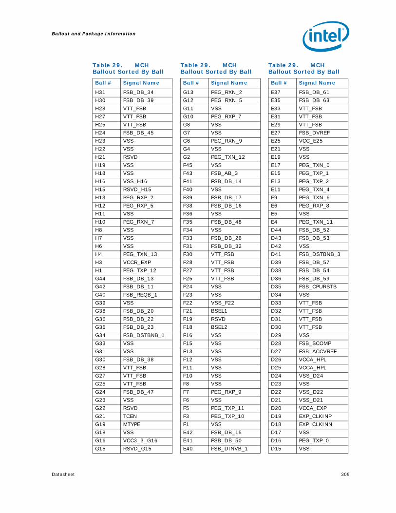
Datasheet 309
Ballout and Package Information
H31 FSB_DB_34
H30 FSB_DB_39
H28 VTT_FSB
H27 VTT_FSB
H25 VTT_FSB
H24 FSB_DB_45
H23 VSS
H22 VSS
H21 RSVD
H19 VSS
H18 VSS
H16 VSS_H16
H15 RSVD_H15
H13 PEG_RXP_2
H12 PEG_RXP_5
H11 VSS
H10 PEG_RXN_7
H8 VSS
H7 VSS
H6 VSS
H4 PEG_TXN_13
H3 VCCR_EXP
H1 PEG_TXP_12
G44 FSB_DB_13
G42 FSB_DB_11
G40 FSB_REQB_1
G39 VSS
G38 FSB_DB_20
G36 FSB_DB_22
G35 FSB_DB_23
G34 FSB_DSTBNB_1
G33 VSS
G31 VSS
G30 FSB_DB_38
G28 VTT_FSB
G27 VTT_FSB
G25 VTT_FSB
G24 FSB_DB_47
G23 VSS
G22 RSVD
G21 TCEN
G19 MTYPE
G18 VSS
G16 VCC3_3_G16
G15 RSVD_G15
Table 29. MCH Ballout Sorted By Ball
Ball # Signal Name
G13 PEG_RXN_2
G12 PEG_RXN_5
G11 VSS
G10 PEG_RXP_7
G8 VSS
G7 VSS
G6 PEG_RXN_9
G4 VSS
G2 PEG_TXN_12
F45 VSS
F43 FSB_AB_3
F41 FSB_DB_14
F40 VSS
F39 FSB_DB_17
F38 FSB_DB_16
F36 VSS
F35 FSB_DB_48
F34 VSS
F33 FSB_DB_26
F31 FSB_DB_32
F30 VTT_FSB
F28 VTT_FSB
F27 VTT_FSB
F25 VTT_FSB
F24 VSS
F23 VSS
F22 VSS_F22
F21 BSEL1
F19 RSVD
F18 BSEL2
F16 VSS
F15 VSS
F13 VSS
F12 VSS
F11 VSS
F10 VSS
F8 VSS
F7 PEG_RXP_9
F6 VSS
F5 PEG_TXP_11
F3 PEG_TXP_10
F1 VSS
E42 FSB_DB_15
E41 FSB_DB_50
E40 FSB_DINVB_1
Table 29. MCH Ballout Sorted By Ball
Ball # Signal Name
E37 FSB_DB_61
E35 FSB_DB_63
E33 VTT_FSB
E31 VTT_FSB
E29 VTT_FSB
E27 FSB_DVREF
E25 VCC_E25
E21 VSS
E19 VSS
E17 PEG_TXN_0
E15 PEG_TXP_1
E13 PEG_TXP_2
E11 PEG_TXN_4
E9 PEG_TXN_6
E6 PEG_RXP_8
E5 VSS
E4 PEG_TXN_11
D44 FSB_DB_52
D43 FSB_DB_53
D42 VSS
D41 FSB_DSTBNB_3
D39 FSB_DB_57
D38 FSB_DB_54
D36 FSB_DB_59
D35 FSB_CPURSTB
D34 VSS
D33 VTT_FSB
D32 VTT_FSB
D31 VTT_FSB
D30 VTT_FSB
D29 VSS
D28 FSB_SCOMP
D27 FSB_ACCVREF
D26 VCCA_HPL
D25 VCCA_HPL
D24 VSS_D24
D23 VSS
D22 VSS_D22
D21 VSS_D21
D20 VCCA_EXP
D19 EXP_CLKINP
D18 EXP_CLKINN
D17 VSS
D16 PEG_TXP_0
D15 VSS
Table 29. MCH Ballout Sorted By Ball
Ball # Signal Name
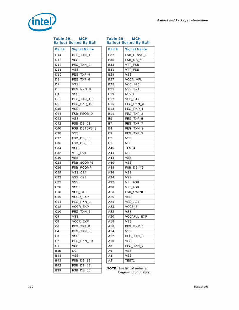
310 Datasheet
Ballout and Package Information
NOTE: See list of notes at beginning of chapter.
D14 PEG_TXN_1
D13 VSS
D12 PEG_TXN_2
D11 VSS
D10 PEG_TXP_4
D8 PEG_TXP_6
D7 VSS
D5 PEG_RXN_8
D4 VSS
D3 PEG_TXN_10
D2 PEG_RXP_10
C45 VSS
C44 FSB_REQB_0
C43 VSS
C42 FSB_DB_51
C40 FSB_DSTBPB_3
C38 VSS
C37 FSB_DB_60
C36 FSB_DB_58
C34 VSS
C32 VTT_FSB
C30 VSS
C28 FSB_SCOMPB
C26 FSB_RCOMP
C24 VSS_C24
C23 VSS_C23
C22 VSS
C20 VSS
C18 VCC_C18
C16 VCCR_EXP
C14 PEG_RXN_1
C12 VCCR_EXP
C10 PEG_TXN_5
C9 VSS
C8 VCCR_EXP
C6 PEG_TXP_8
C4 PEG_TXN_8
C3 VSS
C2 PEG_RXN_10
C1 VSS
B45 NC
B44 VSS
B43 FSB_DB_18
B42 FSB_DB_55
B39 FSB_DB_56
Table 29. MCH Ballout Sorted By Ball
Ball # Signal Name
B37 FSB_DINVB_3
B35 FSB_DB_62
B33 VTT_FSB
B31 VTT_FSB
B29 VSS
B27 VCCA_MPL
B25 VCC_B25
B21 VSS_B21
B19 RSVD
B17 VSS_B17
B15 PEG_RXN_0
B13 PEG_RXP_1
B11 PEG_TXP_3
B9 PEG_TXP_5
B7 PEG_TXP_7
B4 PEG_TXN_9
B3 PEG_TXP_9
B2 VSS
B1 NC
A45 TEST3
A44 NC
A43 VSS
A40 VSS
A38 FSB_DB_49
A36 VSS
A34 VSS
A32 VTT_FSB
A30 VTT_FSB
A28 FSB_SWING
A26 VSS
A24 VSS_A24
A23 VCC3_3
A22 VSS
A20 VCCAPLL_EXP
A18 VSS
A16 PEG_RXP_0
A14 VSS
A12 PEG_TXN_3
A10 VSS
A8 PEG_TXN_7
A6 VSS
A3 VSS
A2 TEST2
Table 29. MCH Ballout Sorted By Ball
Ball # Signal Name
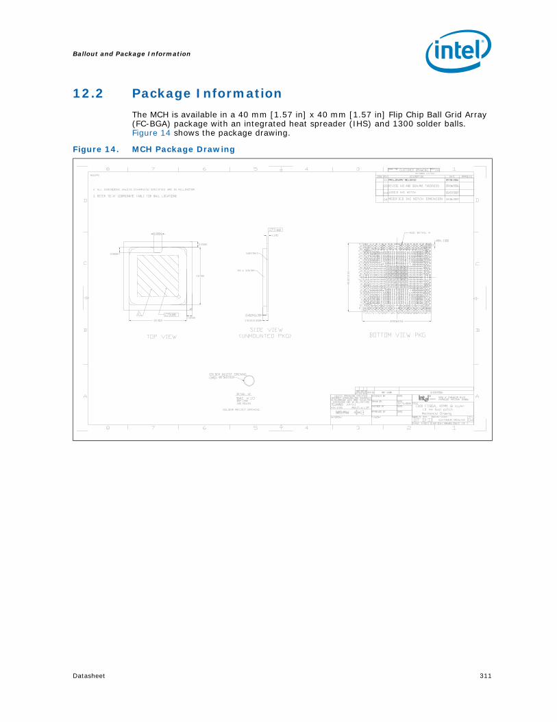
Datasheet 311
Ballout and Package Information
12.2 Package Information
The MCH is available in a 40 mm [1.57 in] x 40 mm [1.57 in] Flip Chip Ball Grid Array (FC-BGA) package with an integrated heat spreader (IHS) and 1300 solder balls. Figure 14 shows the package drawing.
Figure 14. MCH Package Drawing

Ballout and Package Information
312 Datasheet

Datasheet 313
Testability
13 Testability
In the MCH, testability for Automated Test Equipment (ATE) board level testing has been implemented as an XOR chain. An XOR-tree is a chain of XOR gates each with one input pin connected to it which allows for pad to ball to trace connection testing.
The XOR testing methodology is to boot the part using straps to enter XOR mode (A description of the boot process follows). Once in XOR mode, all of the pins of an XOR chain are driven to logic 1. This action will force the output of that XOR chain to either a 1 if the number of the pins making up the chain is even or a 0 if the number of the pins making up the chain is odd.
Once a valid output is detected on the XOR chain output, a walking 0 pattern is moved from one end of the chain to the other. Every time the walking 0 is applied to a pin on the chain, the output will toggle. If the output does not toggle, there is a disconnect somewhere between die, package, and board and the system can be considered a failure.
13.1 XOR Test Mode Initialization
Figure 15. XOR Test Mode Initialization Cycles
PWROK
RSTIN#
STRAP PINS
HCLKP/GCLKP
HCLKN/GCLKN
XOR inputs
XOR output
CL_PWROK
X
CL_RST#

Testability
314 Datasheet
The above figure shows the wave forms to be able to boot the part into XOR mode. The straps that need to be controlled during this boot process are BSEL[2:0], RSVD (Ball L18), EXP_SLR, and XORTEST.
On the X38 Express Chipset platforms, all strap values must be driven before PWROK asserts. BSEL0 must be a 1. BSEL[2:1] need to be defined values, but logic value in any order will do. XORTEST must be driven to 0.
Not all of the pins will be used in all implementations. Due to the need to minimize test points and unnecessary routing, the XOR Chain 14 is dynamic depending on the values of EXP_SLR, and RSVD (Ball L18). See Figure 30 for what parts of XOR Chain 14 become valid XOR inputs depending on the use of EXP_SLR and RSVD (Ball L18).
13.2 XOR Chain Definition
The MCH has 15 XOR chains. The XOR chain outputs are driven out on the following output pins. During fullwidth testing, XOR chain outputs will be visible on both pins.
Table 30. XOR Chain 14 Functionality
RSVD (Ball L18) EXP_SLR XOR Chain 14
1 0
EXP_RXP[15:0]EXP_RXN[15:0]EXP_TXP[15:0]EXP_TXN[15:0]
1 1
EXP_RXP[15:0]EXP_RXN[15:0]EXP_TXP[15:0]EXP_TXN[15:0]
0 0
EXP_RXP[15:8]EXP_RXN[15:8]EXP_TXP[15:8]EXP_TXN[15:8]
0 1
EXP_RXP[7:0]EXP_RXN[7:0]EXP_TXP[7:0]EXP_TXN[7:0]
1 0
EXP_RXP[15:0]EXP_RXN[15:0]EXP_TXP[15:0]EXP_TXN[15:0]
1 1
EXP_RXP[15:0]EXP_RXN[15:0]EXP_TXP[15:0]EXP_TXN[15:0]

Datasheet 315
Testability
13.3 XOR Chains
This section provides the XOR chains.
Table 31. XOR Chain Outputs
XOR Chain Output Pins Coordinate Location
xor_out0 ALLZTEST M21
xor_out1 XORTEST L22
xor_out2 ICH_SYNCB P16
xor_out3 RSVD N18
xor_out4 RSVD AN12
xor_out5 RSVD AM14
xor_out6 BSEL1 F21
xor_out7 BSEL2 F18
xor_out8 RSVD AN13
xor_out9 RSVD AP12
xor_out10 EXP_SLR K19
xor_out11 RSVD L18
xor_out12 BSEL0 M22
xor_out13 RSVD H21
xor_out14 RSVD G22

Testability
316 Datasheet
13.3.1 XOR Chains for DDR2 (No ECC)
Table 32. XOR Chain 0 (DDR2, NoECC)
Pin Count
Ball #
Signal Name
M21 ALLZTEST
1 B39 FSB_DB_56
2 D44 FSB_DB_52
3 B42 FSB_DB_55
4 D39 FSB_DB_57
5 C42 FSB_DB_51
6 C36 FSB_DB_58
7 A38 FSB_DB_49
8 B35 FSB_DB_62
9 D38 FSB_DB_54
10 E41 FSB_DB_50
11 D43 FSB_DB_53
12 D36 FSB_DB_59
13 E35 FSB_DB_63
14 E37 FSB_DB_61
15 F35 FSB_DB_48
16 C37 FSB_DB_60
17 F33 FSB_DB_26
18 B43 FSB_DB_18
19 F39 FSB_DB_17
20 F38 FSB_DB_16
21 H33 FSB_DB_25
22 G36 FSB_DB_22
23 G38 FSB_DB_20
24 G35 FSB_DB_23
25 L36 FSB_DB_19
26 L33 FSB_DB_29
27 L34 FSB_DB_27
28 N33 FSB_DB_28
29 N31 FSB_DB_30
30 K34 FSB_DB_24
31 M31 FSB_DB_31
32 K35 FSB_DB_21
33 L24 FSB_DB_44
34 H24 FSB_DB_45
35 G24 FSB_DB_47
36 K28 FSB_DB_40
37 K24 FSB_DB_46
38 F31 FSB_DB_32
39 L30 FSB_DB_36
40 G30 FSB_DB_38
41 N24 FSB_DB_42
42 H31 FSB_DB_34
43 H30 FSB_DB_39
44 L28 FSB_DB_41
45 M30 FSB_DB_35
46 N30 FSB_DB_37
47 K31 FSB_DB_33
48 L25 FSB_DB_43
49 E42 FSB_DB_15
50 F41 FSB_DB_14
51 G42 FSB_DB_11
52 G44 FSB_DB_13
53 H42 FSB_DB_9
54 J43 FSB_DB_8
55 H45 FSB_DB_12
56 L42 FSB_DB_7
57 M45 FSB_DB_5
58 M42 FSB_DB_3
59 L44 FSB_DB_6
60 J41 FSB_DB_10
61 P42 FSB_DB_0
62 N41 FSB_DB_1
63 N42 FSB_DB_4
64 N44 FSB_DB_2
Table 33. XOR Chain 1 (DDR2, NoECC)
Pin Count
Ball # Signal Name
L22 XORTEST
1 H39 FSB_REQB_4
2 K42 FSB_AB_15
Table 32. XOR Chain 0 (DDR2, NoECC)
Pin Count
Ball #
Signal Name

Testability
Datasheet 317
3 G40 FSB_REQB_1
4 K36 FSB_REQB_3
5 F43 FSB_AB_3
6 M36 FSB_AB_5
7 K38 FSB_AB_6
8 M38 FSB_AB_4
9 L40 FSB_AB_7
10 C44 FSB_REQB_0
11 M40 FSB_ADSTBB_0
12 N40 FSB_AB_9
13 L39 FSB_REQB_2
14 N36 FSB_AB_8
15 N39 FSB_AB_11
16 N38 FSB_AB_13
17 R35 FSB_AB_16
18 N34 FSB_AB_12
19 R39 FSB_AB_14
20 R36 FSB_AB_10
21 T34 FSB_AB_19
22 P43 FSB_AB_21
23 T40 FSB_AB_17
24 W34 FSB_AB_25
25 W36 FSB_AB_30
26 T38 FSB_AB_20
27 V35 FSB_AB_26
28 W33 FSB_AB_27
29 W38 FSB_AB_22
30 V34 FSB_ADSTBB_1
31 AA33 FSB_AB_31
32 T36 FSB_AB_18
33 AB35 FSB_AB_34
34 AA35 FSB_AB_32
35 V38 FSB_AB_23
36 AB34 FSB_AB_29
37 V39 FSB_AB_24
38 AA40 FSB_AB_33
39 V43 FSB_AB_28
40 AA38 FSB_AB_35
Table 33. XOR Chain 1 (DDR2, NoECC)
Pin Count
Ball # Signal Name
Table 34. XOR Chain 2 (DDR2, NoECC)
Pin Count
Ball #
Signal Name
P16 ICH_SYNCB
1 G34 FSB_DSTBNB_1
2 H34 FSB_DSTBPB_1
3 W41 FSB_RSB_1
4 R42 FSB_HITB
5 W40 FSB_TRDYB
6 V42 FSB_HITMB
7 M25 FSB_DSTBNB_2
8 N25 FSB_DSTBPB_2
9 K43 FSB_DSTBNB_0
10 J44 FSB_DSTBPB_0
11 T45 FSB_LOCKB
12 U42 FSB_BNRB
13 H38 FSB_BPRIB
14 D35 FSB_CPURSTB
Table 35. XOR Chain 3 (DDR2, NoECC)
Pin Count
Ball #
Signal Name
N18 RSVD
1 D41 FSB_DSTBNB_3
2 C40 FSB_DSTBPB_3
3 B37 FSB_DINVB_3
4 E40 FSB_DINVB_1
5 T39 FSB_DEFERB
6 R44 FSB_RSB_0
7 U41 FSB_DRDYB
8 T42 FSB_DBSYB
9 R41 FSB_RSB_2
10 N28 FSB_DINVB_2
11 L41 FSB_DINVB_0
12 W44 FSB_BREQ0B
13 U44 FSB_ADSB

Testability
318 Datasheet
Table 36. XOR Chain 4 (DDR2, NoECC)
Pin Count
Ball # Signal Name
AN12 RSVD
1 AY41 DDR_A_ODT_1
2 BB39 DDR_A_CSB_1
3 BD42 DDR_A_CSB_0
4 BD37 DDR_A_MA_10
5 BB43 DDR_A_ODT_0
6 BC36 DDR_A_MA_0
7 BA27 DDR_A_MA_9
8 BB30 DDR_A_MA_2
9 BB29 DDR_A_MA_3
10 BA29 DDR_A_MA_4
11 AV35 DDR_A_CKB_2
12 AT34 DDR_A_CK_2
13 AT33 DDR_A_CK_0
14 AN28 DDR_A_CK_1
15 AR33 DDR_A_CKB_0
16 AM28 DDR_A_CKB_1
17 BD29 DDR_A_MA_6
18 BB31 DDR_A_MA_1
19 BB28 DDR_A_MA_5
20 BC28 DDR_A_MA_8
21 AY27 DDR_A_MA_7
22 AY24 DDR_A_CKE_0
23 BB25 DDR_A_CKE_1
24 AV21 DDR_A_DQSB_3
25 AP21 DDR_A_DM_3
26 AY15 DDR_A_DQSB_2
27 BC14 DDR_A_DM_2
28 AY11 DDR_A_DQSB_1
29 BC10 DDR_A_DM_1
30 BC6 DDR_A_DQSB_0
31 BB5 DDR_A_DM_0
Table 37. XOR Chain 5 (DDR2, NoECC)
Pin Count
Ball # Signal Name
AM14 RSVD
1 AA44 DDR_A_DQSB_7
2 AB40 DDR_A_DM_7
3 AD42 DDR_A_DQSB_6
4 AE44 DDR_A_DM_6
5 AM42 DDR_A_DQSB_5
6 AN44 DDR_A_DM_5
7 AT42 DDR_A_DQSB_4
8 AU44 DDR_A_DM_4
9 BA42 DDR_A_MA_13
10 BB41 DDR_A_CASB
11 BD39 DDR_A_WEB
12 BB36 DDR_A_BS_1
13 BB38 DDR_A_RASB
14 BC37 DDR_A_BS_0
15 BA25 DDR_A_MA_14
16 BD27 DDR_A_MA_11
17 BB26 DDR_A_BS_2
18 BB27 DDR_A_MA_12
19 AK15 CL_DATA
20 AK14 CL_CLK
Table 38. XOR Chain 6 (DDR2, NoECC)
Pin Count
Ball # Signal Name
F21 BSEL1
1 AA42 DDR_A_DQS_7
2 Y42 DDR_A_DQ_58
3 AA41 DDR_A_DQ_62
4 AB42 DDR_A_DQ_56
5 AB43 DDR_A_DQ_57
6 W42 DDR_A_DQ_59
7 AC40 DDR_A_DQ_60
8 Y45 DDR_A_DQ_63
9 AB39 DDR_A_DQ_61

Testability
Datasheet 319
10 AD43 DDR_A_DQS_6
11 AC42 DDR_A_DQ_50
12 AC39 DDR_A_DQ_55
13 AE41 DDR_A_DQ_48
14 AD40 DDR_A_DQ_54
15 AC45 DDR_A_DQ_51
16 AF42 DDR_A_DQ_52
17 AF45 DDR_A_DQ_53
18 AE42 DDR_A_DQ_49
19 AM43 DDR_A_DQS_5
20 AL40 DDR_A_DQ_46
21 AN41 DDR_A_DQ_40
22 AN42 DDR_A_DQ_41
23 AP42 DDR_A_DQ_44
24 AL41 DDR_A_DQ_47
25 AP45 DDR_A_DQ_45
26 AL42 DDR_A_DQ_43
27 AL44 DDR_A_DQ_42
28 AT43 DDR_A_DQS_4
29 AU43 DDR_A_DQ_33
30 AU41 DDR_A_DQ_37
31 AV42 DDR_A_DQ_32
32 AR41 DDR_A_DQ_38
33 AR40 DDR_A_DQ_39
34 AR44 DDR_A_DQ_34
35 AW42 DDR_A_DQ_36
36 AR42 DDR_A_DQ_35
37 AT21 DDR_A_DQS_3
38 AY21 DDR_A_DQ_25
39 AW19 DDR_A_DQ_29
40 AN21 DDR_A_DQ_30
41 AW22 DDR_A_DQ_31
42 AT22 DDR_A_DQ_27
43 AN22 DDR_A_DQ_26
44 AN19 DDR_A_DQ_24
45 AV19 DDR_A_DQ_28
46 BA15 DDR_A_DQS_2
47 BB16 DDR_A_DQ_18
48 BD15 DDR_A_DQ_22
Table 38. XOR Chain 6 (DDR2, NoECC)
Pin Count
Ball # Signal Name
49 BE16 DDR_A_DQ_19
50 BB14 DDR_A_DQ_17
51 BB15 DDR_A_DQ_23
52 BA13 DDR_A_DQ_20
53 BD13 DDR_A_DQ_16
54 BB13 DDR_A_DQ_21
55 BA11 DDR_A_DQS_1
56 BC9 DDR_A_DQ_13
57 BD11 DDR_A_DQ_14
58 BB11 DDR_A_DQ_15
59 BE12 DDR_A_DQ_11
60 BD9 DDR_A_DQ_8
61 BA9 DDR_A_DQ_12
62 BB12 DDR_A_DQ_10
63 BB10 DDR_A_DQ_9
64 BA6 DDR_A_DQS_0
65 BB7 DDR_A_DQ_7
66 BB8 DDR_A_DQ_2
67 BE8 DDR_A_DQ_3
68 BD7 DDR_A_DQ_6
69 BD4 DDR_A_DQ_1
70 BC4 DDR_A_DQ_0
71 BB4 DDR_A_DQ_5
72 BD3 DDR_A_DQ_4
Table 39. XOR Chain 7 (DDR2, NoECC)
Pin Count
Ball # Signal Name
F18 BSEL2
1 AW44 DDR_A_ODT_3
2 AY43 DDR_A_CSB_3
3 BA41 DDR_A_ODT_2
4 BB39 DDR_A_CSB_2
5 AV31 DDR_A_CK_3
6 AT31 DDR_A_CKB_3
7 AT36 DDR_A_CKB_5
8 AT35 DDR_A_CK_5
Table 38. XOR Chain 6 (DDR2, NoECC)
Pin Count
Ball # Signal Name
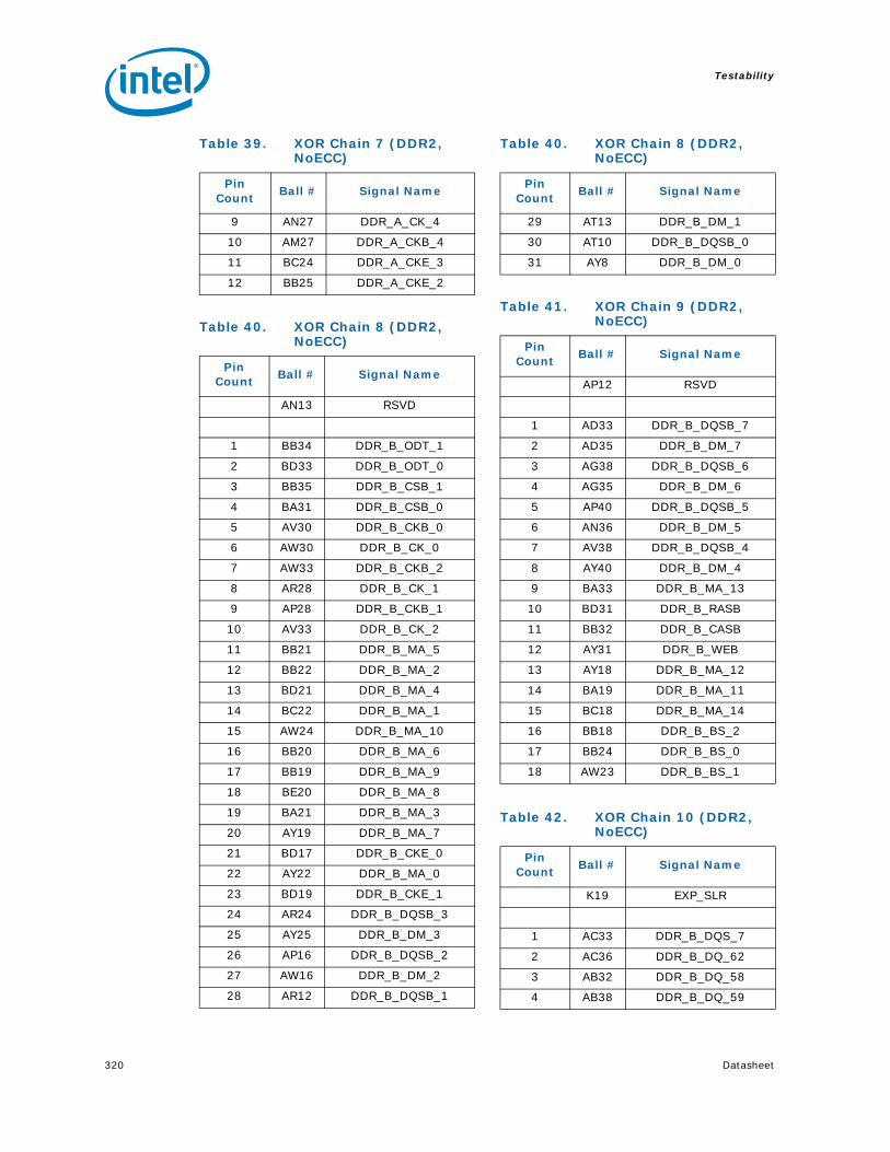
Testability
320 Datasheet
9 AN27 DDR_A_CK_4
10 AM27 DDR_A_CKB_4
11 BC24 DDR_A_CKE_3
12 BB25 DDR_A_CKE_2
Table 40. XOR Chain 8 (DDR2, NoECC)
Pin Count
Ball # Signal Name
AN13 RSVD
1 BB34 DDR_B_ODT_1
2 BD33 DDR_B_ODT_0
3 BB35 DDR_B_CSB_1
4 BA31 DDR_B_CSB_0
5 AV30 DDR_B_CKB_0
6 AW30 DDR_B_CK_0
7 AW33 DDR_B_CKB_2
8 AR28 DDR_B_CK_1
9 AP28 DDR_B_CKB_1
10 AV33 DDR_B_CK_2
11 BB21 DDR_B_MA_5
12 BB22 DDR_B_MA_2
13 BD21 DDR_B_MA_4
14 BC22 DDR_B_MA_1
15 AW24 DDR_B_MA_10
16 BB20 DDR_B_MA_6
17 BB19 DDR_B_MA_9
18 BE20 DDR_B_MA_8
19 BA21 DDR_B_MA_3
20 AY19 DDR_B_MA_7
21 BD17 DDR_B_CKE_0
22 AY22 DDR_B_MA_0
23 BD19 DDR_B_CKE_1
24 AR24 DDR_B_DQSB_3
25 AY25 DDR_B_DM_3
26 AP16 DDR_B_DQSB_2
27 AW16 DDR_B_DM_2
28 AR12 DDR_B_DQSB_1
Table 39. XOR Chain 7 (DDR2, NoECC)
Pin Count
Ball # Signal Name
29 AT13 DDR_B_DM_1
30 AT10 DDR_B_DQSB_0
31 AY8 DDR_B_DM_0
Table 41. XOR Chain 9 (DDR2, NoECC)
Pin Count
Ball # Signal Name
AP12 RSVD
1 AD33 DDR_B_DQSB_7
2 AD35 DDR_B_DM_7
3 AG38 DDR_B_DQSB_6
4 AG35 DDR_B_DM_6
5 AP40 DDR_B_DQSB_5
6 AN36 DDR_B_DM_5
7 AV38 DDR_B_DQSB_4
8 AY40 DDR_B_DM_4
9 BA33 DDR_B_MA_13
10 BD31 DDR_B_RASB
11 BB32 DDR_B_CASB
12 AY31 DDR_B_WEB
13 AY18 DDR_B_MA_12
14 BA19 DDR_B_MA_11
15 BC18 DDR_B_MA_14
16 BB18 DDR_B_BS_2
17 BB24 DDR_B_BS_0
18 AW23 DDR_B_BS_1
Table 42. XOR Chain 10 (DDR2, NoECC)
Pin Count
Ball # Signal Name
K19 EXP_SLR
1 AC33 DDR_B_DQS_7
2 AC36 DDR_B_DQ_62
3 AB32 DDR_B_DQ_58
4 AB38 DDR_B_DQ_59
Table 40. XOR Chain 8 (DDR2, NoECC)
Pin Count
Ball # Signal Name
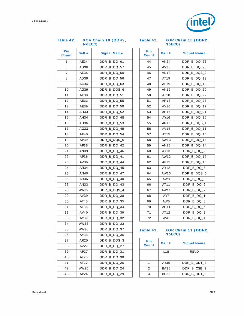
Testability
Datasheet 321
5 AE34 DDR_B_DQ_61
6 AD36 DDR_B_DQ_57
7 AE35 DDR_B_DQ_60
8 AD39 DDR_B_DQ_56
9 AC34 DDR_B_DQ_63
10 AG39 DDR_B_DQS_6
11 AE38 DDR_B_DQ_51
12 AE33 DDR_B_DQ_55
13 AE39 DDR_B_DQ_50
14 AH33 DDR_B_DQ_52
15 AH34 DDR_B_DQ_48
16 AH36 DDR_B_DQ_53
17 AG33 DDR_B_DQ_49
18 AE40 DDR_B_DQ_54
19 AP39 DDR_B_DQS_5
20 AP35 DDR_B_DQ_42
21 AN39 DDR_B_DQ_46
22 AP36 DDR_B_DQ_41
23 AV36 DDR_B_DQ_44
24 AR34 DDR_B_DQ_45
25 AN40 DDR_B_DQ_47
26 AR36 DDR_B_DQ_40
27 AN33 DDR_B_DQ_43
28 AW39 DDR_B_DQS_4
29 AV39 DDR_B_DQ_38
30 AT40 DDR_B_DQ_35
31 AT38 DDR_B_DQ_34
32 AV40 DDR_B_DQ_39
33 AY39 DDR_B_DQ_32
34 AW38 DDR_B_DQ_33
35 AW36 DDR_B_DQ_37
36 AY38 DDR_B_DQ_36
37 AR25 DDR_B_DQS_3
38 AV27 DDR_B_DQ_27
39 AP27 DDR_B_DQ_31
40 AT25 DDR_B_DQ_30
41 AT27 DDR_B_DQ_26
42 AW25 DDR_B_DQ_24
43 AP24 DDR_B_DQ_29
Table 42. XOR Chain 10 (DDR2, NoECC)
Pin Count
Ball # Signal Name
44 AN24 DDR_B_DQ_28
45 AV25 DDR_B_DQ_25
46 AN18 DDR_B_DQS_2
47 AT19 DDR_B_DQ_19
48 AP19 DDR_B_DQ_18
49 AN16 DDR_B_DQ_20
50 AT18 DDR_B_DQ_22
51 AR18 DDR_B_DQ_23
52 AV16 DDR_B_DQ_17
53 AR16 DDR_B_DQ_21
54 AY16 DDR_B_DQ_16
55 AR13 DDR_B_DQS_1
56 AV15 DDR_B_DQ_11
57 AT15 DDR_B_DQ_10
58 AW13 DDR_B_DQ_13
59 AN15 DDR_B_DQ_14
60 AY13 DDR_B_DQ_9
61 AW12 DDR_B_DQ_12
62 AP15 DDR_B_DQ_15
63 AY12 DDR_B_DQ_8
64 AW10 DDR_B_DQS_0
65 AW8 DDR_B_DQ_0
66 AT11 DDR_B_DQ_2
67 AW11 DDR_B_DQ_7
68 AY7 DDR_B_DQ_1
69 AW6 DDR_B_DQ_5
70 AR11 DDR_B_DQ_6
71 AT12 DDR_B_DQ_3
72 AV8 DDR_B_DQ_4
Table 43. XOR Chain 11 (DDR2, NoECC)
Pin Count
Ball # Signal Name
L18 RSVD
1 AY35 DDR_B_ODT_3
2 BA35 DDR_B_CSB_3
3 BB33 DDR_B_ODT_2
Table 42. XOR Chain 10 (DDR2, NoECC)
Pin Count
Ball # Signal Name

Testability
322 Datasheet
4 BC32 DDR_B_CSB_2
5 AY34 DDR_B_CKB_5
6 AW34 DDR_B_CK_5
7 AY28 DDR_B_CKB_4
8 AY30 DDR_B_CK_4
9 AP31 DDR_B_CKB_3
10 AR31 DDR_B_CK_3
11 BA17 DDR_B_CKE_3
12 BB17 DDR_B_CKE_2
Table 44. XOR Chain 12 (DDR2, NoECC)
Pin Count
Ball #
Signal Name
M22 BSEL0
1 V10 DMI_TXP_3
2 V11 DMI_TXN_3
3 V7 DMI_RXP_3
4 V6 DMI_RXN_3
5 R2 DMI_TXP_2
6 T1 DMI_TXN_2
7 P4 DMI_RXP_2
8 R5 DMI_RXN_2
9 N2 DMI_TXP_1
10 P3 DMI_TXN_1
11 T7 DMI_RXP_1
12 T8 DMI_RXN_1
13 R7 DMI_TXP_0
14 R6 DMI_TXN_0
15 N5 DMI_RXP_0
16 M4 DMI_RXN_0
Table 43. XOR Chain 11 (DDR2, NoECC)
Pin Count
Ball # Signal Name
Table 45. XOR Chain 13 (DDR2, NoECC)
Pin Count
Ball #
Signal Name
H21 RSVD
1 A8 PEG_TXN_7
2 B7 PEG_TXP_7
3 H10 PEG_RXN_7
4 G10 PEG_RXP_7
5 E9 PEG_TXN_6
6 D8 PEG_TXP_6
7 L12 PEG_RXN_6
8 K11 PEG_RXP_6
9 C10 PEG_TXN_5
10 B9 PEG_TXP_5
11 G12 PEG_RXN_5
12 H12 PEG_RXP_5
13 E11 PEG_TXN_4
14 D10 PEG_TXP_4
15 M13 PEG_RXN_4
16 N13 PEG_RXP_4
17 A12 PEG_TXN_3
18 B11 PEG_TXP_3
19 K13 PEG_RXN_3
20 L13 PEG_RXP_3
21 D12 PEG_TXN_2
22 E13 PEG_TXP_2
23 G13 PEG_RXN_2
24 H13 PEG_RXP_2
25 D14 PEG_TXN_1
26 E15 PEG_TXP_1
27 C14 PEG_RXN_1
28 B13 PEG_RXP_1
29 E17 PEG_TXN_0
30 D16 PEG_TXP_0
31 B15 PEG_RXN_0
32 A16 PEG_RXP_0
33 L2 PEG_TXN_15
34 M1 PEG_TXP_15
35 N10 PEG_RXN_15
36 N8 PEG_RXP_15
37 K4 PEG_TXN_14

Testability
Datasheet 323
38 L5 PEG_TXP_14
39 J2 PEG_RXN_14
40 K3 PEG_RXP_14
41 H4 PEG_TXN_13
42 J5 PEG_TXP_13
43 M8 PEG_RXN_13
44 M7 PEG_RXP_13
45 G2 PEG_TXN_12
46 H1 PEG_TXP_12
47 L10 PEG_RXN_12
48 M11 PEG_RXP_12
49 E4 PEG_TXN_11
50 F5 PEG_TXP_11
51 K8 PEG_RXN_11
52 K7 PEG_RXP_11
53 D3 PEG_TXN_10
54 F3 PEG_TXP_10
55 C2 PEG_RXN_10
56 D2 PEG_RXP_10
57 B4 PEG_TXN_9
58 B3 PEG_TXP_9
59 G6 PEG_RXN_9
60 F7 PEG_RXP_9
61 C4 PEG_TXN_8
62 C6 PEG_TXP_8
63 D5 PEG_RXN_8
64 E6 PEG_RXP_8
Table 46. XOR Chain 14 (DDR2, NoECC)
Pin Count
Ball # Signal Name
G22 RSVD
1 AJ5 PEG2_TXN_7
2 AK4 PEG2_TXP_7
3 AE11 PEG2_RXN_7
4 AE10 PEG2_RXP_7
5 AH3 PEG2_TXN_6
Table 45. XOR Chain 13 (DDR2, NoECC)
Pin Count
Ball #
Signal Name
6 AJ2 PEG2_TXP_6
7 AD12 PEG2_RXN_6
8 AE13 PEG2_RXP_6
9 AG5 PEG2_TXN_5
10 AH4 PEG2_TXP_5
11 AC7 PEG2_RXN_5
12 AC6 PEG2_RXP_5
13 AF1 PEG2_TXN_4
14 AG2 PEG2_TXP_4
15 AC10 PEG2_RXN_4
16 AC11 PEG2_RXP_4
17 AE5 PEG2_TXN_3
18 AF4 PEG2_TXP_3
19 AB12 PEG2_RXN_3
20 AC13 PEG2_RXP_3
21 AD3 PEG2_TXN_2
22 AE2 PEG2_TXP_2
23 AA7 PEG2_RXN_2
24 AA6 PEG2_RXP_2
25 AC4 PEG2_TXN_1
26 AD4 PEG2_TXP_1
27 AA11 PEG2_RXN_1
28 AA10 PEG2_RXP_1
29 AB1 PEG2_TXN_0
30 AB3 PEG2_TXP_0
31 AA13 PEG2_RXN_0
32 W12 PEG2_RXP_0
33 AP6 PEG2_TXN_15
34 AP7 PEG2_TXP_15
35 AP11 PEG2_RXN_15
36 AP10 PEG2_RXP_15
37 AT3 PEG2_TXN_14
38 AU2 PEG2_TXP_14
39 AL7 PEG2_RXN_14
40 AL6 PEG2_RXP_14
41 AR5 PEG2_TXN_13
42 AT4 PEG2_TXP_13
43 AL10 PEG2_RXN_13
44 AL11 PEG2_RXP_13
Table 46. XOR Chain 14 (DDR2, NoECC)
Pin Count
Ball # Signal Name

Testability
324 Datasheet
45 AP1 PEG2_TXN_12
46 AR2 PEG2_TXP_12
47 AK13 PEG2_RXN_12
48 AK12 PEG2_RXP_12
49 AN5 PEG2_TXN_11
50 AP4 PEG2_TXP_11
51 AH6 PEG2_RXN_11
52 AH7 PEG2_RXP_11
53 AM3 PEG2_TXN_10
54 AN2 PEG2_TXP_10
55 AH10 PEG2_RXN_10
56 AH11 PEG2_RXP_10
57 AL5 PEG2_TXN_9
58 AM4 PEG2_TXP_9
59 AH13 PEG2_RXN_9
60 AG12 PEG2_RXP_9
61 AK1 PEG2_TXN_8
62 AL2 PEG2_TXP_8
63 AE6 PEG2_RXN_8
64 AE7 PEG2_RXP_8
Table 46. XOR Chain 14 (DDR2, NoECC)
Pin Count
Ball # Signal Name

Testability
Datasheet 325
13.3.2 XOR Chains for DDR2 (ECC)
Table 47. XOR Chain 0 (DDR2, ECC)
Pin Count
Ball #
Signal Name
M21 ALLZTEST
1 B39 FSB_DB_56
2 D44 FSB_DB_52
3 B42 FSB_DB_55
4 D39 FSB_DB_57
5 C42 FSB_DB_51
6 C36 FSB_DB_58
7 A38 FSB_DB_49
8 B35 FSB_DB_62
9 D38 FSB_DB_54
10 E41 FSB_DB_50
11 D43 FSB_DB_53
12 D36 FSB_DB_59
13 E35 FSB_DB_63
14 E37 FSB_DB_61
15 F35 FSB_DB_48
16 C37 FSB_DB_60
17 F33 FSB_DB_26
18 B43 FSB_DB_18
19 F39 FSB_DB_17
20 F38 FSB_DB_16
21 H33 FSB_DB_25
22 G36 FSB_DB_22
23 G38 FSB_DB_20
24 G35 FSB_DB_23
25 L36 FSB_DB_19
26 L33 FSB_DB_29
27 L34 FSB_DB_27
28 N33 FSB_DB_28
29 N31 FSB_DB_30
30 K34 FSB_DB_24
31 M31 FSB_DB_31
32 K35 FSB_DB_21
33 L24 FSB_DB_44
34 H24 FSB_DB_45
35 G24 FSB_DB_47
36 K28 FSB_DB_40
37 K24 FSB_DB_46
38 F31 FSB_DB_32
39 L30 FSB_DB_36
40 G30 FSB_DB_38
41 N24 FSB_DB_42
42 H31 FSB_DB_34
43 H30 FSB_DB_39
44 L28 FSB_DB_41
45 M30 FSB_DB_35
46 N30 FSB_DB_37
47 K31 FSB_DB_33
48 L25 FSB_DB_43
49 E42 FSB_DB_15
50 F41 FSB_DB_14
51 G42 FSB_DB_11
52 G44 FSB_DB_13
53 H42 FSB_DB_9
54 J43 FSB_DB_8
55 H45 FSB_DB_12
56 L42 FSB_DB_7
57 M45 FSB_DB_5
58 M42 FSB_DB_3
59 L44 FSB_DB_6
60 J41 FSB_DB_10
61 P42 FSB_DB_0
62 N41 FSB_DB_1
63 N42 FSB_DB_4
64 N44 FSB_DB_2
Table 47. XOR Chain 0 (DDR2, ECC)
Pin Count
Ball #
Signal Name

Testability
326 Datasheet
Table 48. XOR Chain 1 (DDR2, ECC)
Pin Count
Ball # Signal Name
L22 XORTEST
1 H39 FSB_REQB_4
2 K42 FSB_AB_15
3 G40 FSB_REQB_1
4 K36 FSB_REQB_3
5 F43 FSB_AB_3
6 M36 FSB_AB_5
7 K38 FSB_AB_6
8 M38 FSB_AB_4
9 L40 FSB_AB_7
10 C44 FSB_REQB_0
11 M40 FSB_ADSTBB_0
12 N40 FSB_AB_9
13 L39 FSB_REQB_2
14 N36 FSB_AB_8
15 N39 FSB_AB_11
16 N38 FSB_AB_13
17 R35 FSB_AB_16
18 N34 FSB_AB_12
19 R39 FSB_AB_14
20 R36 FSB_AB_10
21 T34 FSB_AB_19
22 P43 FSB_AB_21
23 T40 FSB_AB_17
24 W34 FSB_AB_25
25 W36 FSB_AB_30
26 T38 FSB_AB_20
27 V35 FSB_AB_26
28 W33 FSB_AB_27
29 W38 FSB_AB_22
30 V34 FSB_ADSTBB_1
31 AA33 FSB_AB_31
32 T36 FSB_AB_18
33 AB35 FSB_AB_34
34 AA35 FSB_AB_32
35 V38 FSB_AB_23
36 AB34 FSB_AB_29
37 V39 FSB_AB_24
38 AA40 FSB_AB_33
39 V43 FSB_AB_28
40 AA38 FSB_AB_35
Table 49. XOR Chain 2 (DDR2, ECC)
Pin Count
Ball #
Signal Name
P16 ICH_SYNCB
1 G34 FSB_DSTBNB_1
2 H34 FSB_DSTBPB_1
3 W41 FSB_RSB_1
4 R42 FSB_HITB
5 W40 FSB_TRDYB
6 V42 FSB_HITMB
7 M25 FSB_DSTBNB_2
8 N25 FSB_DSTBPB_2
9 K43 FSB_DSTBNB_0
10 J44 FSB_DSTBPB_0
11 T45 FSB_LOCKB
12 U42 FSB_BNRB
13 H38 FSB_BPRIB
14 D35 FSB_CPURSTB
Table 50. XOR Chain 3 (DDR2, ECC)
Pin Count
Ball #
Signal Name
N18 RSVD
1 D41 FSB_DSTBNB_3
2 C40 FSB_DSTBPB_3
3 B37 FSB_DINVB_3
4 E40 FSB_DINVB_1
5 T39 FSB_DEFERB
6 R44 FSB_RSB_0
7 U41 FSB_DRDYB
8 T42 FSB_DBSYB
9 R41 FSB_RSB_2
10 N28 FSB_DINVB_2
11 L41 FSB_DINVB_0
12 W44 FSB_BREQ0B
13 U44 FSB_ADSB

Testability
Datasheet 327
Table 51. XOR Chain 4 (DDR2, ECC)
Pin Count
Ball # Signal Name
AN12 RSVD
1 AK35 DDR_A_CB_3
2 AL33 DDR_A_CB_0
3 AK34 DDR_A_CB_6
4 AK33 DDR_A_CB_4
5 AK39 DDR_A_CB_7
6 AN35 DDR_A_CB_1
7 AL34 DDR_A_CB_5
8 AK38 DDR_A_CB_2
9 AY41 DDR_A_ODT_1
10 BB39 DDR_A_CSB_1
11 BD42 DDR_A_CSB_0
12 BD37 DDR_A_MA_10
13 BB43 DDR_A_ODT_0
14 BC36 DDR_A_MA_0
15 BA27 DDR_A_MA_9
16 BB30 DDR_A_MA_2
17 BB29 DDR_A_MA_3
18 BA29 DDR_A_MA_4
19 AV35 DDR_A_CKB_2
20 AT34 DDR_A_CK_2
21 AT33 DDR_A_CK_0
22 AN28 DDR_A_CK_1
23 AR33 DDR_A_CKB_0
24 AM28 DDR_A_CKB_1
25 BD29 DDR_A_MA_6
26 BB31 DDR_A_MA_1
27 BB28 DDR_A_MA_5
28 BC28 DDR_A_MA_8
29 AY27 DDR_A_MA_7
30 AY24 DDR_A_CKE_0
31 BB25 DDR_A_CKE_1
32 AV21 DDR_A_DQSB_3
33 AP21 DDR_A_DM_3
34 AY15 DDR_A_DQSB_2
35 BC14 DDR_A_DM_2
36 AY11 DDR_A_DQSB_1
37 BC10 DDR_A_DM_1
38 BC6 DDR_A_DQSB_0
39 BB5 DDR_A_DM_0
Table 52. XOR Chain 5 (DDR2, ECC)
Pin Count
Ball # Signal Name
AM14 RSVD
1 AA44 DDR_A_DQSB_7
2 AB40 DDR_A_DM_7
3 AD42 DDR_A_DQSB_6
4 AE44 DDR_A_DM_6
5 AL36 DDR_A_DQSB_8
6 AM42 DDR_A_DQSB_5
7 AN44 DDR_A_DM_5
8 AT42 DDR_A_DQSB_4
9 AU44 DDR_A_DM_4
10 BA42 DDR_A_MA_13
11 BB41 DDR_A_CASB
12 BD39 DDR_A_WEB
13 BB36 DDR_A_BS_1
14 BB38 DDR_A_RASB
15 BC37 DDR_A_BS_0
16 BA25 DDR_A_MA_14
17 BD27 DDR_A_MA_11
18 BB26 DDR_A_BS_2
19 BB27 DDR_A_MA_12
20 AK15 CL_DATA
21 AK14 CL_CLK
Table 51. XOR Chain 4 (DDR2, ECC)
Pin Count
Ball # Signal Name

Testability
328 Datasheet
Table 53. XOR Chain 6 (DDR2, ECC)
Pin Count
Ball # Signal Name
F21 BSEL1
1 AA42 DDR_A_DQS_7
2 Y42 DDR_A_DQ_58
3 AA41 DDR_A_DQ_62
4 AB42 DDR_A_DQ_56
5 AB43 DDR_A_DQ_57
6 W42 DDR_A_DQ_59
7 AC40 DDR_A_DQ_60
8 Y45 DDR_A_DQ_63
9 AB39 DDR_A_DQ_61
10 AD43 DDR_A_DQS_6
11 AC42 DDR_A_DQ_50
12 AC39 DDR_A_DQ_55
13 AE41 DDR_A_DQ_48
14 AD40 DDR_A_DQ_54
15 AC45 DDR_A_DQ_51
16 AF42 DDR_A_DQ_52
17 AF45 DDR_A_DQ_53
18 AE42 DDR_A_DQ_49
19 AL38 DDR_A_DQS_8
20 AM43 DDR_A_DQS_5
21 AL40 DDR_A_DQ_46
22 AN41 DDR_A_DQ_40
23 AN42 DDR_A_DQ_41
24 AP42 DDR_A_DQ_44
25 AL41 DDR_A_DQ_47
26 AP45 DDR_A_DQ_45
27 AL42 DDR_A_DQ_43
28 AL44 DDR_A_DQ_42
29 AT43 DDR_A_DQS_4
30 AU43 DDR_A_DQ_33
31 AU41 DDR_A_DQ_37
32 AV42 DDR_A_DQ_32
33 AR41 DDR_A_DQ_38
34 AR40 DDR_A_DQ_39
35 AR44 DDR_A_DQ_34
36 AW42 DDR_A_DQ_36
37 AR42 DDR_A_DQ_35
38 AT21 DDR_A_DQS_3
39 AY21 DDR_A_DQ_25
40 AW19 DDR_A_DQ_29
41 AN21 DDR_A_DQ_30
42 AW22 DDR_A_DQ_31
43 AT22 DDR_A_DQ_27
44 AN22 DDR_A_DQ_26
45 AN19 DDR_A_DQ_24
46 AV19 DDR_A_DQ_28
47 BA15 DDR_A_DQS_2
48 BB16 DDR_A_DQ_18
49 BD15 DDR_A_DQ_22
50 BE16 DDR_A_DQ_19
51 BB14 DDR_A_DQ_17
52 BB15 DDR_A_DQ_23
53 BA13 DDR_A_DQ_20
54 BD13 DDR_A_DQ_16
55 BB13 DDR_A_DQ_21
56 BA11 DDR_A_DQS_1
57 BC9 DDR_A_DQ_13
58 BD11 DDR_A_DQ_14
59 BB11 DDR_A_DQ_15
60 BE12 DDR_A_DQ_11
61 BD9 DDR_A_DQ_8
62 BA9 DDR_A_DQ_12
63 BB12 DDR_A_DQ_10
64 BB10 DDR_A_DQ_9
65 BA6 DDR_A_DQS_0
66 BB7 DDR_A_DQ_7
67 BB8 DDR_A_DQ_2
68 BE8 DDR_A_DQ_3
69 BD7 DDR_A_DQ_6
70 BD4 DDR_A_DQ_1
71 BC4 DDR_A_DQ_0
72 BB4 DDR_A_DQ_5
73 BD3 DDR_A_DQ_4
Table 53. XOR Chain 6 (DDR2, ECC)
Pin Count
Ball # Signal Name

Testability
Datasheet 329
Table 54. XOR Chain 7 (DDR2, ECC)
Pin Count
Ball # Signal Name
F18 BSEL2
1 AW44 DDR_A_ODT_3
2 AY43 DDR_A_CSB_3
3 BA41 DDR_A_ODT_2
4 BB39 DDR_A_CSB_2
5 AV31 DDR_A_CK_3
6 AT31 DDR_A_CKB_3
7 AT36 DDR_A_CKB_5
8 AT35 DDR_A_CK_5
9 AN27 DDR_A_CK_4
10 AM27 DDR_A_CKB_4
11 BC24 DDR_A_CKE_3
12 BB25 DDR_A_CKE_2
Table 55. XOR Chain 8 (DDR2, ECC)
Pin Count
Ball # Signal Name
AN13 RSVD
1 AG42 DDR_B_CB_2
2 AG44 DDR_B_CB_7
3 AG41 DDR_B_CB_6
4 AK45 DDR_B_CB_0
5 AJ42 DDR_B_CB_4
6 AG40 DDR_B_CB_3
7 AJ44 DDR_B_CB_1
8 AK42 DDR_B_CB_5
9 BB34 DDR_B_ODT_1
10 BD33 DDR_B_ODT_0
11 BB35 DDR_B_CSB_1
12 BA31 DDR_B_CSB_0
13 AV30 DDR_B_CKB_0
14 AW30 DDR_B_CK_0
15 AW33 DDR_B_CKB_2
16 AR28 DDR_B_CK_1
17 AP28 DDR_B_CKB_1
18 AV33 DDR_B_CK_2
19 BB21 DDR_B_MA_5
20 BB22 DDR_B_MA_2
21 BD21 DDR_B_MA_4
22 BC22 DDR_B_MA_1
23 AW24 DDR_B_MA_10
24 BB20 DDR_B_MA_6
25 BB19 DDR_B_MA_9
26 BE20 DDR_B_MA_8
27 BA21 DDR_B_MA_3
28 AY19 DDR_B_MA_7
29 BD17 DDR_B_CKE_0
30 AY22 DDR_B_MA_0
31 BD19 DDR_B_CKE_1
32 AR24 DDR_B_DQSB_3
33 AY25 DDR_B_DM_3
34 AP16 DDR_B_DQSB_2
35 AW16 DDR_B_DM_2
36 AR12 DDR_B_DQSB_1
37 AT13 DDR_B_DM_1
38 AT10 DDR_B_DQSB_0
39 AY8 DDR_B_DM_0
Table 56. XOR Chain 9 (DDR2, ECC)
Pin Count
Ball # Signal Name
AP12 RSVD
1 AD33 DDR_B_DQSB_7
2 AD35 DDR_B_DM_7
3 AG38 DDR_B_DQSB_6
4 AG35 DDR_B_DM_6
5 AH42 DDR_B_DQSB_8
6 AP40 DDR_B_DQSB_5
7 AN36 DDR_B_DM_5
8 AV38 DDR_B_DQSB_4
Table 55. XOR Chain 8 (DDR2, ECC)
Pin Count
Ball # Signal Name

Testability
330 Datasheet
9 AY40 DDR_B_DM_4
10 BA33 DDR_B_MA_13
11 BD31 DDR_B_RASB
12 BB32 DDR_B_CASB
13 AY31 DDR_B_WEB
14 AY18 DDR_B_MA_12
15 BA19 DDR_B_MA_11
16 BC18 DDR_B_MA_14
17 BB18 DDR_B_BS_2
18 BB24 DDR_B_BS_0
19 AW23 DDR_B_BS_1
Table 57. XOR Chain 10 (DDR2, ECC)
Pin Count
Ball # Signal Name
K19 EXP_SLR
1 AC33 DDR_B_DQS_7
2 AC36 DDR_B_DQ_62
3 AB32 DDR_B_DQ_58
4 AB38 DDR_B_DQ_59
5 AE34 DDR_B_DQ_61
6 AD36 DDR_B_DQ_57
7 AE35 DDR_B_DQ_60
8 AD39 DDR_B_DQ_56
9 AC34 DDR_B_DQ_63
10 AG39 DDR_B_DQS_6
11 AE38 DDR_B_DQ_51
12 AE33 DDR_B_DQ_55
13 AE39 DDR_B_DQ_50
14 AH33 DDR_B_DQ_52
15 AH34 DDR_B_DQ_48
16 AH36 DDR_B_DQ_53
17 AG33 DDR_B_DQ_49
18 AE40 DDR_B_DQ_54
19 AH43 DDR_B_DQS_8
20 AP39 DDR_B_DQS_5
Table 56. XOR Chain 9 (DDR2, ECC)
Pin Count
Ball # Signal Name
21 AP35 DDR_B_DQ_42
22 AN39 DDR_B_DQ_46
23 AP36 DDR_B_DQ_41
24 AV36 DDR_B_DQ_44
25 AR34 DDR_B_DQ_45
26 AN40 DDR_B_DQ_47
27 AR36 DDR_B_DQ_40
28 AN33 DDR_B_DQ_43
29 AW39 DDR_B_DQS_4
30 AV39 DDR_B_DQ_38
31 AT40 DDR_B_DQ_35
32 AT38 DDR_B_DQ_34
33 AV40 DDR_B_DQ_39
34 AY39 DDR_B_DQ_32
35 AW38 DDR_B_DQ_33
36 AW36 DDR_B_DQ_37
37 AY38 DDR_B_DQ_36
38 AR25 DDR_B_DQS_3
39 AV27 DDR_B_DQ_27
40 AP27 DDR_B_DQ_31
41 AT25 DDR_B_DQ_30
42 AT27 DDR_B_DQ_26
43 AW25 DDR_B_DQ_24
44 AP24 DDR_B_DQ_29
45 AN24 DDR_B_DQ_28
46 AV25 DDR_B_DQ_25
47 AN18 DDR_B_DQS_2
48 AT19 DDR_B_DQ_19
49 AP19 DDR_B_DQ_18
50 AN16 DDR_B_DQ_20
51 AT18 DDR_B_DQ_22
52 AR18 DDR_B_DQ_23
53 AV16 DDR_B_DQ_17
54 AR16 DDR_B_DQ_21
55 AY16 DDR_B_DQ_16
56 AR13 DDR_B_DQS_1
57 AV15 DDR_B_DQ_11
58 AT15 DDR_B_DQ_10
59 AW13 DDR_B_DQ_13
Table 57. XOR Chain 10 (DDR2, ECC)
Pin Count
Ball # Signal Name

Testability
Datasheet 331
60 AN15 DDR_B_DQ_14
61 AY13 DDR_B_DQ_9
62 AW12 DDR_B_DQ_12
63 AP15 DDR_B_DQ_15
64 AY12 DDR_B_DQ_8
65 AW10 DDR_B_DQS_0
66 AW8 DDR_B_DQ_0
67 AT11 DDR_B_DQ_2
68 AW11 DDR_B_DQ_7
69 AY7 DDR_B_DQ_1
70 AW6 DDR_B_DQ_5
71 AR11 DDR_B_DQ_6
72 AT12 DDR_B_DQ_3
73 AV8 DDR_B_DQ_4
Table 58. XOR Chain 11 (DDR2, ECC)
Pin Count
Ball # Signal Name
L18 RSVD
1 AY35 DDR_B_ODT_3
2 BA35 DDR_B_CSB_3
3 BB33 DDR_B_ODT_2
4 BC32 DDR_B_CSB_2
5 AY34 DDR_B_CKB_5
6 AW34 DDR_B_CK_5
7 AY28 DDR_B_CKB_4
8 AY30 DDR_B_CK_4
9 AP31 DDR_B_CKB_3
10 AR31 DDR_B_CK_3
11 BA17 DDR_B_CKE_3
12 BB17 DDR_B_CKE_2
Table 57. XOR Chain 10 (DDR2, ECC)
Pin Count
Ball # Signal Name
Table 59. XOR Chain 12 (DDR2, ECC)
Pin Count
Ball #
Signal Name
M22 BSEL0
1 V10 DMI_TXP_3
2 V11 DMI_TXN_3
3 V7 DMI_RXP_3
4 V6 DMI_RXN_3
5 R2 DMI_TXP_2
6 T1 DMI_TXN_2
7 P4 DMI_RXP_2
8 R5 DMI_RXN_2
9 N2 DMI_TXP_1
10 P3 DMI_TXN_1
11 T7 DMI_RXP_1
12 T8 DMI_RXN_1
13 R7 DMI_TXP_0
14 R6 DMI_TXN_0
15 N5 DMI_RXP_0
16 M4 DMI_RXN_0
Table 60. XOR Chain 13 (DDR2, ECC)
Pin Count
Ball #
Signal Name
H21 RSVD
1 A8 PEG_TXN_7
2 B7 PEG_TXP_7
3 H10 PEG_RXN_7
4 G10 PEG_RXP_7
5 E9 PEG_TXN_6
6 D8 PEG_TXP_6
7 L12 PEG_RXN_6
8 K11 PEG_RXP_6
9 C10 PEG_TXN_5
10 B9 PEG_TXP_5
11 G12 PEG_RXN_5
12 H12 PEG_RXP_5
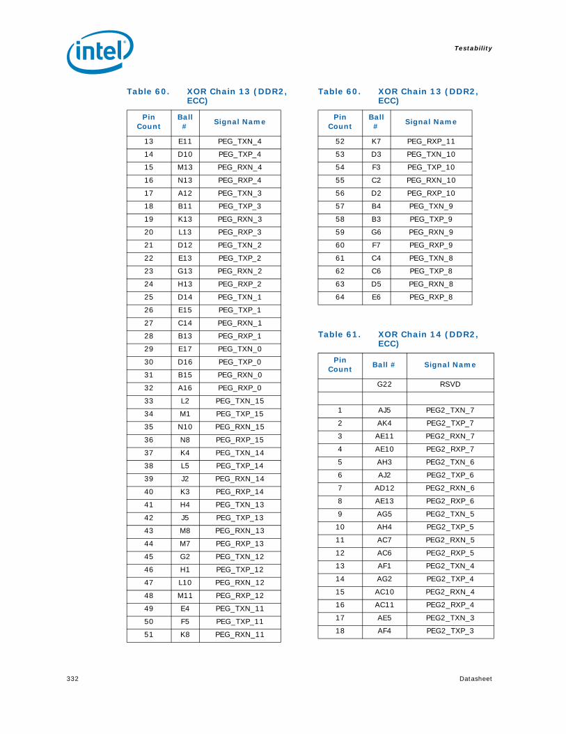
Testability
332 Datasheet
13 E11 PEG_TXN_4
14 D10 PEG_TXP_4
15 M13 PEG_RXN_4
16 N13 PEG_RXP_4
17 A12 PEG_TXN_3
18 B11 PEG_TXP_3
19 K13 PEG_RXN_3
20 L13 PEG_RXP_3
21 D12 PEG_TXN_2
22 E13 PEG_TXP_2
23 G13 PEG_RXN_2
24 H13 PEG_RXP_2
25 D14 PEG_TXN_1
26 E15 PEG_TXP_1
27 C14 PEG_RXN_1
28 B13 PEG_RXP_1
29 E17 PEG_TXN_0
30 D16 PEG_TXP_0
31 B15 PEG_RXN_0
32 A16 PEG_RXP_0
33 L2 PEG_TXN_15
34 M1 PEG_TXP_15
35 N10 PEG_RXN_15
36 N8 PEG_RXP_15
37 K4 PEG_TXN_14
38 L5 PEG_TXP_14
39 J2 PEG_RXN_14
40 K3 PEG_RXP_14
41 H4 PEG_TXN_13
42 J5 PEG_TXP_13
43 M8 PEG_RXN_13
44 M7 PEG_RXP_13
45 G2 PEG_TXN_12
46 H1 PEG_TXP_12
47 L10 PEG_RXN_12
48 M11 PEG_RXP_12
49 E4 PEG_TXN_11
50 F5 PEG_TXP_11
51 K8 PEG_RXN_11
Table 60. XOR Chain 13 (DDR2, ECC)
Pin Count
Ball #
Signal Name
52 K7 PEG_RXP_11
53 D3 PEG_TXN_10
54 F3 PEG_TXP_10
55 C2 PEG_RXN_10
56 D2 PEG_RXP_10
57 B4 PEG_TXN_9
58 B3 PEG_TXP_9
59 G6 PEG_RXN_9
60 F7 PEG_RXP_9
61 C4 PEG_TXN_8
62 C6 PEG_TXP_8
63 D5 PEG_RXN_8
64 E6 PEG_RXP_8
Table 61. XOR Chain 14 (DDR2, ECC)
Pin Count
Ball # Signal Name
G22 RSVD
1 AJ5 PEG2_TXN_7
2 AK4 PEG2_TXP_7
3 AE11 PEG2_RXN_7
4 AE10 PEG2_RXP_7
5 AH3 PEG2_TXN_6
6 AJ2 PEG2_TXP_6
7 AD12 PEG2_RXN_6
8 AE13 PEG2_RXP_6
9 AG5 PEG2_TXN_5
10 AH4 PEG2_TXP_5
11 AC7 PEG2_RXN_5
12 AC6 PEG2_RXP_5
13 AF1 PEG2_TXN_4
14 AG2 PEG2_TXP_4
15 AC10 PEG2_RXN_4
16 AC11 PEG2_RXP_4
17 AE5 PEG2_TXN_3
18 AF4 PEG2_TXP_3
Table 60. XOR Chain 13 (DDR2, ECC)
Pin Count
Ball #
Signal Name

Testability
Datasheet 333
19 AB12 PEG2_RXN_3
20 AC13 PEG2_RXP_3
21 AD3 PEG2_TXN_2
22 AE2 PEG2_TXP_2
23 AA7 PEG2_RXN_2
24 AA6 PEG2_RXP_2
25 AC4 PEG2_TXN_1
26 AD4 PEG2_TXP_1
27 AA11 PEG2_RXN_1
28 AA10 PEG2_RXP_1
29 AB1 PEG2_TXN_0
30 AB3 PEG2_TXP_0
31 AA13 PEG2_RXN_0
32 W12 PEG2_RXP_0
33 AP6 PEG2_TXN_15
34 AP7 PEG2_TXP_15
35 AP11 PEG2_RXN_15
36 AP10 PEG2_RXP_15
37 AT3 PEG2_TXN_14
38 AU2 PEG2_TXP_14
39 AL7 PEG2_RXN_14
40 AL6 PEG2_RXP_14
41 AR5 PEG2_TXN_13
42 AT4 PEG2_TXP_13
43 AL10 PEG2_RXN_13
44 AL11 PEG2_RXP_13
45 AP1 PEG2_TXN_12
46 AR2 PEG2_TXP_12
47 AK13 PEG2_RXN_12
48 AK12 PEG2_RXP_12
49 AN5 PEG2_TXN_11
50 AP4 PEG2_TXP_11
51 AH6 PEG2_RXN_11
52 AH7 PEG2_RXP_11
53 AM3 PEG2_TXN_10
54 AN2 PEG2_TXP_10
55 AH10 PEG2_RXN_10
56 AH11 PEG2_RXP_10
57 AL5 PEG2_TXN_9
Table 61. XOR Chain 14 (DDR2, ECC)
Pin Count
Ball # Signal Name
58 AM4 PEG2_TXP_9
59 AH13 PEG2_RXN_9
60 AG12 PEG2_RXP_9
61 AK1 PEG2_TXN_8
62 AL2 PEG2_TXP_8
63 AE6 PEG2_RXN_8
64 AE7 PEG2_RXP_8
Table 61. XOR Chain 14 (DDR2, ECC)
Pin Count
Ball # Signal Name

Testability
334 Datasheet
13.3.3 XOR Chains for DDR3 (No ECC)
Table 62. XOR Chain 0 (DDR3, NoECC)
Pin Count
Ball #
Signal Name
M21 ALLZTEST
1 B39 FSB_DB_56
2 D44 FSB_DB_52
3 B42 FSB_DB_55
4 D39 FSB_DB_57
5 C42 FSB_DB_51
6 C36 FSB_DB_58
7 A38 FSB_DB_49
8 B35 FSB_DB_62
9 D38 FSB_DB_54
10 E41 FSB_DB_50
11 D43 FSB_DB_53
12 D36 FSB_DB_59
13 E35 FSB_DB_63
14 E37 FSB_DB_61
15 F35 FSB_DB_48
16 C37 FSB_DB_60
17 F33 FSB_DB_26
18 B43 FSB_DB_18
19 F39 FSB_DB_17
20 F38 FSB_DB_16
21 H33 FSB_DB_25
22 G36 FSB_DB_22
23 G38 FSB_DB_20
24 G35 FSB_DB_23
25 L36 FSB_DB_19
26 L33 FSB_DB_29
27 L34 FSB_DB_27
28 N33 FSB_DB_28
29 N31 FSB_DB_30
30 K34 FSB_DB_24
31 M31 FSB_DB_31
32 K35 FSB_DB_21
33 L24 FSB_DB_44
34 H24 FSB_DB_45
35 G24 FSB_DB_47
36 K28 FSB_DB_40
37 K24 FSB_DB_46
38 F31 FSB_DB_32
39 L30 FSB_DB_36
40 G30 FSB_DB_38
41 N24 FSB_DB_42
42 H31 FSB_DB_34
43 H30 FSB_DB_39
44 L28 FSB_DB_41
45 M30 FSB_DB_35
46 N30 FSB_DB_37
47 K31 FSB_DB_33
48 L25 FSB_DB_43
49 E42 FSB_DB_15
50 F41 FSB_DB_14
51 G42 FSB_DB_11
52 G44 FSB_DB_13
53 H42 FSB_DB_9
54 J43 FSB_DB_8
55 H45 FSB_DB_12
56 L42 FSB_DB_7
57 M45 FSB_DB_5
58 M42 FSB_DB_3
59 L44 FSB_DB_6
60 J41 FSB_DB_10
61 P42 FSB_DB_0
62 N41 FSB_DB_1
63 N42 FSB_DB_4
64 N44 FSB_DB_2
Table 63. XOR Chain 1 (DDR3, NoECC)
Pin Count
Ball # Signal Name
L22 XORTEST
1 H39 FSB_REQB_4
2 K42 FSB_AB_15
Table 62. XOR Chain 0 (DDR3, NoECC)
Pin Count
Ball #
Signal Name

Testability
Datasheet 335
3 G40 FSB_REQB_1
4 K36 FSB_REQB_3
5 F43 FSB_AB_3
6 M36 FSB_AB_5
7 K38 FSB_AB_6
8 M38 FSB_AB_4
9 L40 FSB_AB_7
10 C44 FSB_REQB_0
11 M40 FSB_ADSTBB_0
12 N40 FSB_AB_9
13 L39 FSB_REQB_2
14 N36 FSB_AB_8
15 N39 FSB_AB_11
16 N38 FSB_AB_13
17 R35 FSB_AB_16
18 N34 FSB_AB_12
19 R39 FSB_AB_14
20 R36 FSB_AB_10
21 T34 FSB_AB_19
22 P43 FSB_AB_21
23 T40 FSB_AB_17
24 W34 FSB_AB_25
25 W36 FSB_AB_30
26 T38 FSB_AB_20
27 V35 FSB_AB_26
28 W33 FSB_AB_27
29 W38 FSB_AB_22
30 V34 FSB_ADSTBB_1
31 AA33 FSB_AB_31
32 T36 FSB_AB_18
33 AB35 FSB_AB_34
34 AA35 FSB_AB_32
35 V38 FSB_AB_23
36 AB34 FSB_AB_29
37 V39 FSB_AB_24
38 AA40 FSB_AB_33
39 V43 FSB_AB_28
40 AA38 FSB_AB_35
Table 63. XOR Chain 1 (DDR3, NoECC)
Pin Count
Ball # Signal Name
Table 64. XOR Chain 2 (DDR3, NoECC)
Pin Count
Ball #
Signal Name
P16 ICH_SYNCB
1 G34 FSB_DSTBNB_1
2 H34 FSB_DSTBPB_1
3 W41 FSB_RSB_1
4 R42 FSB_HITB
5 W40 FSB_TRDYB
6 V42 FSB_HITMB
7 M25 FSB_DSTBNB_2
8 N25 FSB_DSTBPB_2
9 K43 FSB_DSTBNB_0
10 J44 FSB_DSTBPB_0
11 T45 FSB_LOCKB
12 U42 FSB_BNRB
13 H38 FSB_BPRIB
14 D35 FSB_CPURSTB
Table 65. XOR Chain 3 (DDR3, NoECC)
Pin Count
Ball #
Signal Name
N18 RSVD
1 D41 FSB_DSTBNB_3
2 C40 FSB_DSTBPB_3
3 B37 FSB_DINVB_3
4 E40 FSB_DINVB_1
5 T39 FSB_DEFERB
6 R44 FSB_RSB_0
7 U41 FSB_DRDYB
8 T42 FSB_DBSYB
9 R41 FSB_RSB_2
10 N28 FSB_DINVB_2
11 L41 FSB_DINVB_0
12 W44 FSB_BREQ0B
13 U44 FSB_ADSB
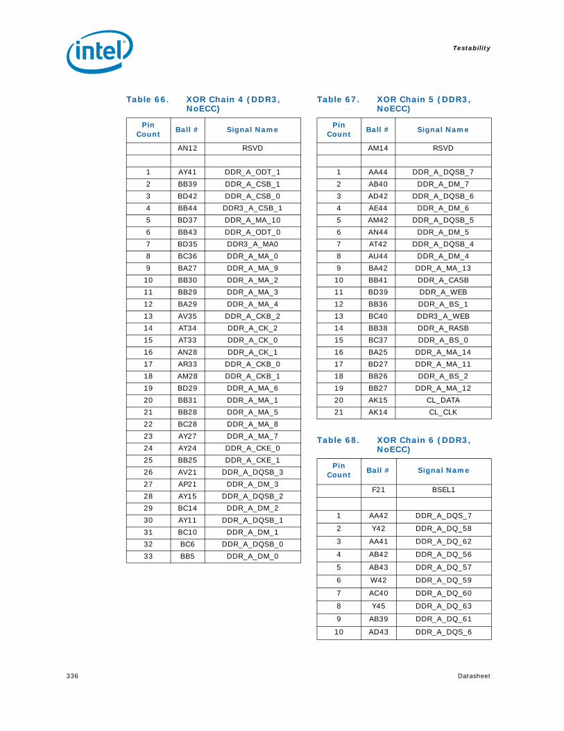
Testability
336 Datasheet
Table 66. XOR Chain 4 (DDR3, NoECC)
Pin Count
Ball # Signal Name
AN12 RSVD
1 AY41 DDR_A_ODT_1
2 BB39 DDR_A_CSB_1
3 BD42 DDR_A_CSB_0
4 BB44 DDR3_A_CSB_1
5 BD37 DDR_A_MA_10
6 BB43 DDR_A_ODT_0
7 BD35 DDR3_A_MA0
8 BC36 DDR_A_MA_0
9 BA27 DDR_A_MA_9
10 BB30 DDR_A_MA_2
11 BB29 DDR_A_MA_3
12 BA29 DDR_A_MA_4
13 AV35 DDR_A_CKB_2
14 AT34 DDR_A_CK_2
15 AT33 DDR_A_CK_0
16 AN28 DDR_A_CK_1
17 AR33 DDR_A_CKB_0
18 AM28 DDR_A_CKB_1
19 BD29 DDR_A_MA_6
20 BB31 DDR_A_MA_1
21 BB28 DDR_A_MA_5
22 BC28 DDR_A_MA_8
23 AY27 DDR_A_MA_7
24 AY24 DDR_A_CKE_0
25 BB25 DDR_A_CKE_1
26 AV21 DDR_A_DQSB_3
27 AP21 DDR_A_DM_3
28 AY15 DDR_A_DQSB_2
29 BC14 DDR_A_DM_2
30 AY11 DDR_A_DQSB_1
31 BC10 DDR_A_DM_1
32 BC6 DDR_A_DQSB_0
33 BB5 DDR_A_DM_0
Table 67. XOR Chain 5 (DDR3, NoECC)
Pin Count
Ball # Signal Name
AM14 RSVD
1 AA44 DDR_A_DQSB_7
2 AB40 DDR_A_DM_7
3 AD42 DDR_A_DQSB_6
4 AE44 DDR_A_DM_6
5 AM42 DDR_A_DQSB_5
6 AN44 DDR_A_DM_5
7 AT42 DDR_A_DQSB_4
8 AU44 DDR_A_DM_4
9 BA42 DDR_A_MA_13
10 BB41 DDR_A_CASB
11 BD39 DDR_A_WEB
12 BB36 DDR_A_BS_1
13 BC40 DDR3_A_WEB
14 BB38 DDR_A_RASB
15 BC37 DDR_A_BS_0
16 BA25 DDR_A_MA_14
17 BD27 DDR_A_MA_11
18 BB26 DDR_A_BS_2
19 BB27 DDR_A_MA_12
20 AK15 CL_DATA
21 AK14 CL_CLK
Table 68. XOR Chain 6 (DDR3, NoECC)
Pin Count
Ball # Signal Name
F21 BSEL1
1 AA42 DDR_A_DQS_7
2 Y42 DDR_A_DQ_58
3 AA41 DDR_A_DQ_62
4 AB42 DDR_A_DQ_56
5 AB43 DDR_A_DQ_57
6 W42 DDR_A_DQ_59
7 AC40 DDR_A_DQ_60
8 Y45 DDR_A_DQ_63
9 AB39 DDR_A_DQ_61
10 AD43 DDR_A_DQS_6

Testability
Datasheet 337
11 AC42 DDR_A_DQ_50
12 AC39 DDR_A_DQ_55
13 AE41 DDR_A_DQ_48
14 AD40 DDR_A_DQ_54
15 AC45 DDR_A_DQ_51
16 AF42 DDR_A_DQ_52
17 AF45 DDR_A_DQ_53
18 AE42 DDR_A_DQ_49
19 AM43 DDR_A_DQS_5
20 AL40 DDR_A_DQ_46
21 AN41 DDR_A_DQ_40
22 AN42 DDR_A_DQ_41
23 AP42 DDR_A_DQ_44
24 AL41 DDR_A_DQ_47
25 AP45 DDR_A_DQ_45
26 AL42 DDR_A_DQ_43
27 AL44 DDR_A_DQ_42
28 AT43 DDR_A_DQS_4
29 AU43 DDR_A_DQ_33
30 AU41 DDR_A_DQ_37
31 AV42 DDR_A_DQ_32
32 AR41 DDR_A_DQ_38
33 AR40 DDR_A_DQ_39
34 AR44 DDR_A_DQ_34
35 AW42 DDR_A_DQ_36
36 AR42 DDR_A_DQ_35
37 AT21 DDR_A_DQS_3
38 AY21 DDR_A_DQ_25
39 AW19 DDR_A_DQ_29
40 AN21 DDR_A_DQ_30
41 AW22 DDR_A_DQ_31
42 AT22 DDR_A_DQ_27
43 AN22 DDR_A_DQ_26
44 AN19 DDR_A_DQ_24
45 AV19 DDR_A_DQ_28
46 BA15 DDR_A_DQS_2
47 BB16 DDR_A_DQ_18
48 BD15 DDR_A_DQ_22
49 BE16 DDR_A_DQ_19
Table 68. XOR Chain 6 (DDR3, NoECC)
Pin Count
Ball # Signal Name
50 BB14 DDR_A_DQ_17
51 BB15 DDR_A_DQ_23
52 BA13 DDR_A_DQ_20
53 BD13 DDR_A_DQ_16
54 BB13 DDR_A_DQ_21
55 BA11 DDR_A_DQS_1
56 BC9 DDR_A_DQ_13
57 BD11 DDR_A_DQ_14
58 BB11 DDR_A_DQ_15
59 BE12 DDR_A_DQ_11
60 BD9 DDR_A_DQ_8
61 BA9 DDR_A_DQ_12
62 BB12 DDR_A_DQ_10
63 BB10 DDR_A_DQ_9
64 BA6 DDR_A_DQS_0
65 BB7 DDR_A_DQ_7
66 BB8 DDR_A_DQ_2
67 BE8 DDR_A_DQ_3
68 BD7 DDR_A_DQ_6
69 BD4 DDR_A_DQ_1
70 BC4 DDR_A_DQ_0
71 BB4 DDR_A_DQ_5
72 BD3 DDR_A_DQ_4
Table 69. XOR Chain 7 (DDR3, NoECC)
Pin Count
Ball # Signal Name
F18 BSEL2
1 AW44 DDR_A_ODT_3
2 AY43 DDR_A_CSB_3
3 BA41 DDR_A_ODT_2
4 BB39 DDR_A_CSB_2
5 AV31 DDR_A_CK_3
6 AT31 DDR_A_CKB_3
7 AT36 DDR_A_CKB_5
8 AT35 DDR_A_CK_5
9 AN27 DDR_A_CK_4
Table 68. XOR Chain 6 (DDR3, NoECC)
Pin Count
Ball # Signal Name

Testability
338 Datasheet
10 AM27 DDR_A_CKB_4
11 BC24 DDR_A_CKE_3
12 BB25 DDR_A_CKE_2
13 BB23 DDR3_DRAMRSTB
Table 70. XOR Chain 8 (DDR3, NoECC)
Pin Count
Ball # Signal Name
AN13 RSVD
1 BB34 DDR_B_ODT_1
2 BD33 DDR_B_ODT_0
3 BB35 DDR_B_CSB_1
4 BA31 DDR_B_CSB_0
5 AV30 DDR_B_CKB_0
6 AW30 DDR_B_CK_0
7 AW33 DDR_B_CKB_2
8 AR28 DDR_B_CK_1
9 AP28 DDR_B_CKB_1
10 AV33 DDR_B_CK_2
11 BB21 DDR_B_MA_5
12 BB22 DDR_B_MA_2
13 BD21 DDR_B_MA_4
14 BC22 DDR_B_MA_1
15 AW24 DDR_B_MA_10
16 BB20 DDR_B_MA_6
17 BB19 DDR_B_MA_9
18 BE20 DDR_B_MA_8
19 BA21 DDR_B_MA_3
20 AY19 DDR_B_MA_7
21 BD17 DDR_B_CKE_0
22 AY22 DDR_B_MA_0
23 BD19 DDR_B_CKE_1
24 AR24 DDR_B_DQSB_3
25 AY25 DDR_B_DM_3
26 AP16 DDR_B_DQSB_2
27 AW16 DDR_B_DM_2
28 AR12 DDR_B_DQSB_1
Table 69. XOR Chain 7 (DDR3, NoECC)
Pin Count
Ball # Signal Name
29 AT13 DDR_B_DM_1
30 AT10 DDR_B_DQSB_0
31 AY8 DDR_B_DM_0
Table 71. XOR Chain 9 (DDR3, NoECC)
Pin Count
Ball # Signal Name
AP12 RSVD
1 AD33 DDR_B_DQSB_7
2 AD35 DDR_B_DM_7
3 AG38 DDR_B_DQSB_6
4 AG35 DDR_B_DM_6
5 AP40 DDR_B_DQSB_5
6 AN36 DDR_B_DM_5
7 AV38 DDR_B_DQSB_4
8 AY40 DDR_B_DM_4
9 BA33 DDR_B_MA_13
10 BD31 DDR_B_RASB
11 BB32 DDR_B_CASB
12 AY31 DDR_B_WEB
13 AY18 DDR_B_MA_12
14 BA19 DDR_B_MA_11
15 BC18 DDR_B_MA_14
16 BB18 DDR_B_BS_2
17 BB24 DDR_B_BS_0
18 AW23 DDR_B_BS_1
Table 72. XOR Chain 10 (DDR3, NoECC)
Pin Count
Ball # Signal Name
K19 EXP_SLR
1 AC33 DDR_B_DQS_7
2 AC36 DDR_B_DQ_62
3 AB32 DDR_B_DQ_58
4 AB38 DDR_B_DQ_59
Table 70. XOR Chain 8 (DDR3, NoECC)
Pin Count
Ball # Signal Name

Testability
Datasheet 339
5 AE34 DDR_B_DQ_61
6 AD36 DDR_B_DQ_57
7 AE35 DDR_B_DQ_60
8 AD39 DDR_B_DQ_56
9 AC34 DDR_B_DQ_63
10 AG39 DDR_B_DQS_6
11 AE38 DDR_B_DQ_51
12 AE33 DDR_B_DQ_55
13 AE39 DDR_B_DQ_50
14 AH33 DDR_B_DQ_52
15 AH34 DDR_B_DQ_48
16 AH36 DDR_B_DQ_53
17 AG33 DDR_B_DQ_49
18 AE40 DDR_B_DQ_54
19 AP39 DDR_B_DQS_5
20 AP35 DDR_B_DQ_42
21 AN39 DDR_B_DQ_46
22 AP36 DDR_B_DQ_41
23 AV36 DDR_B_DQ_44
24 AR34 DDR_B_DQ_45
25 AN40 DDR_B_DQ_47
26 AR36 DDR_B_DQ_40
27 AN33 DDR_B_DQ_43
28 AW39 DDR_B_DQS_4
29 AV39 DDR_B_DQ_38
30 AT40 DDR_B_DQ_35
31 AT38 DDR_B_DQ_34
32 AV40 DDR_B_DQ_39
33 AY39 DDR_B_DQ_32
34 AW38 DDR_B_DQ_33
35 AW36 DDR_B_DQ_37
36 AY38 DDR_B_DQ_36
37 AR25 DDR_B_DQS_3
38 AV27 DDR_B_DQ_27
39 AP27 DDR_B_DQ_31
40 AT25 DDR_B_DQ_30
41 AT27 DDR_B_DQ_26
42 AW25 DDR_B_DQ_24
43 AP24 DDR_B_DQ_29
Table 72. XOR Chain 10 (DDR3, NoECC)
Pin Count
Ball # Signal Name
44 AN24 DDR_B_DQ_28
45 AV25 DDR_B_DQ_25
46 AN18 DDR_B_DQS_2
47 AT19 DDR_B_DQ_19
48 AP19 DDR_B_DQ_18
49 AN16 DDR_B_DQ_20
50 AT18 DDR_B_DQ_22
51 AR18 DDR_B_DQ_23
52 AV16 DDR_B_DQ_17
53 AR16 DDR_B_DQ_21
54 AY16 DDR_B_DQ_16
55 AR13 DDR_B_DQS_1
56 AV15 DDR_B_DQ_11
57 AT15 DDR_B_DQ_10
58 AW13 DDR_B_DQ_13
59 AN15 DDR_B_DQ_14
60 AY13 DDR_B_DQ_9
61 AW12 DDR_B_DQ_12
62 AP15 DDR_B_DQ_15
63 AY12 DDR_B_DQ_8
64 AW10 DDR_B_DQS_0
65 AW8 DDR_B_DQ_0
66 AT11 DDR_B_DQ_2
67 AW11 DDR_B_DQ_7
68 AY7 DDR_B_DQ_1
69 AW6 DDR_B_DQ_5
70 AR11 DDR_B_DQ_6
71 AT12 DDR_B_DQ_3
72 AV8 DDR_B_DQ_4
Table 73. XOR Chain 11 (DDR3, NoECC)
Pin Count
Ball # Signal Name
L18 RSVD
1 AY35 DDR_B_ODT_3
2 BA35 DDR_B_CSB_3
3 BB33 DDR_B_ODT_2
Table 72. XOR Chain 10 (DDR3, NoECC)
Pin Count
Ball # Signal Name

Testability
340 Datasheet
4 BA37 DDR3_B_ODT3
5 BC32 DDR_B_CSB_2
6 AY34 DDR_B_CKB_5
7 AW34 DDR_B_CK_5
8 AY28 DDR_B_CKB_4
9 AY30 DDR_B_CK_4
10 AP31 DDR_B_CKB_3
11 AR31 DDR_B_CK_3
12 BA17 DDR_B_CKE_3
13 BB17 DDR_B_CKE_2
Table 74. XOR Chain 12 (DDR3, NoECC)
Pin Count
Ball #
Signal Name
M22 BSEL0
1 V10 DMI_TXP_3
2 V11 DMI_TXN_3
3 V7 DMI_RXP_3
4 V6 DMI_RXN_3
5 R2 DMI_TXP_2
6 T1 DMI_TXN_2
7 P4 DMI_RXP_2
8 R5 DMI_RXN_2
9 N2 DMI_TXP_1
10 P3 DMI_TXN_1
11 T7 DMI_RXP_1
12 T8 DMI_RXN_1
13 R7 DMI_TXP_0
14 R6 DMI_TXN_0
15 N5 DMI_RXP_0
16 M4 DMI_RXN_0
Table 73. XOR Chain 11 (DDR3, NoECC)
Pin Count
Ball # Signal Name
Table 75. XOR Chain 13 (DDR3, NoECC)
Pin Count
Ball #
Signal Name
H21 RSVD
1 A8 PEG_TXN_7
2 B7 PEG_TXP_7
3 H10 PEG_RXN_7
4 G10 PEG_RXP_7
5 E9 PEG_TXN_6
6 D8 PEG_TXP_6
7 L12 PEG_RXN_6
8 K11 PEG_RXP_6
9 C10 PEG_TXN_5
10 B9 PEG_TXP_5
11 G12 PEG_RXN_5
12 H12 PEG_RXP_5
13 E11 PEG_TXN_4
14 D10 PEG_TXP_4
15 M13 PEG_RXN_4
16 N13 PEG_RXP_4
17 A12 PEG_TXN_3
18 B11 PEG_TXP_3
19 K13 PEG_RXN_3
20 L13 PEG_RXP_3
21 D12 PEG_TXN_2
22 E13 PEG_TXP_2
23 G13 PEG_RXN_2
24 H13 PEG_RXP_2
25 D14 PEG_TXN_1
26 E15 PEG_TXP_1
27 C14 PEG_RXN_1
28 B13 PEG_RXP_1
29 E17 PEG_TXN_0
30 D16 PEG_TXP_0
31 B15 PEG_RXN_0
32 A16 PEG_RXP_0
33 L2 PEG_TXN_15
34 M1 PEG_TXP_15
35 N10 PEG_RXN_15
36 N8 PEG_RXP_15
37 K4 PEG_TXN_14
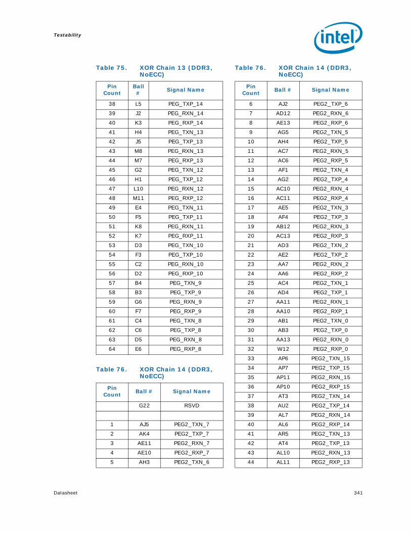
Testability
Datasheet 341
38 L5 PEG_TXP_14
39 J2 PEG_RXN_14
40 K3 PEG_RXP_14
41 H4 PEG_TXN_13
42 J5 PEG_TXP_13
43 M8 PEG_RXN_13
44 M7 PEG_RXP_13
45 G2 PEG_TXN_12
46 H1 PEG_TXP_12
47 L10 PEG_RXN_12
48 M11 PEG_RXP_12
49 E4 PEG_TXN_11
50 F5 PEG_TXP_11
51 K8 PEG_RXN_11
52 K7 PEG_RXP_11
53 D3 PEG_TXN_10
54 F3 PEG_TXP_10
55 C2 PEG_RXN_10
56 D2 PEG_RXP_10
57 B4 PEG_TXN_9
58 B3 PEG_TXP_9
59 G6 PEG_RXN_9
60 F7 PEG_RXP_9
61 C4 PEG_TXN_8
62 C6 PEG_TXP_8
63 D5 PEG_RXN_8
64 E6 PEG_RXP_8
Table 76. XOR Chain 14 (DDR3, NoECC)
Pin Count
Ball # Signal Name
G22 RSVD
1 AJ5 PEG2_TXN_7
2 AK4 PEG2_TXP_7
3 AE11 PEG2_RXN_7
4 AE10 PEG2_RXP_7
5 AH3 PEG2_TXN_6
Table 75. XOR Chain 13 (DDR3, NoECC)
Pin Count
Ball #
Signal Name
6 AJ2 PEG2_TXP_6
7 AD12 PEG2_RXN_6
8 AE13 PEG2_RXP_6
9 AG5 PEG2_TXN_5
10 AH4 PEG2_TXP_5
11 AC7 PEG2_RXN_5
12 AC6 PEG2_RXP_5
13 AF1 PEG2_TXN_4
14 AG2 PEG2_TXP_4
15 AC10 PEG2_RXN_4
16 AC11 PEG2_RXP_4
17 AE5 PEG2_TXN_3
18 AF4 PEG2_TXP_3
19 AB12 PEG2_RXN_3
20 AC13 PEG2_RXP_3
21 AD3 PEG2_TXN_2
22 AE2 PEG2_TXP_2
23 AA7 PEG2_RXN_2
24 AA6 PEG2_RXP_2
25 AC4 PEG2_TXN_1
26 AD4 PEG2_TXP_1
27 AA11 PEG2_RXN_1
28 AA10 PEG2_RXP_1
29 AB1 PEG2_TXN_0
30 AB3 PEG2_TXP_0
31 AA13 PEG2_RXN_0
32 W12 PEG2_RXP_0
33 AP6 PEG2_TXN_15
34 AP7 PEG2_TXP_15
35 AP11 PEG2_RXN_15
36 AP10 PEG2_RXP_15
37 AT3 PEG2_TXN_14
38 AU2 PEG2_TXP_14
39 AL7 PEG2_RXN_14
40 AL6 PEG2_RXP_14
41 AR5 PEG2_TXN_13
42 AT4 PEG2_TXP_13
43 AL10 PEG2_RXN_13
44 AL11 PEG2_RXP_13
Table 76. XOR Chain 14 (DDR3, NoECC)
Pin Count
Ball # Signal Name

Testability
342 Datasheet
§ §
45 AP1 PEG2_TXN_12
46 AR2 PEG2_TXP_12
47 AK13 PEG2_RXN_12
48 AK12 PEG2_RXP_12
49 AN5 PEG2_TXN_11
50 AP4 PEG2_TXP_11
51 AH6 PEG2_RXN_11
52 AH7 PEG2_RXP_11
53 AM3 PEG2_TXN_10
54 AN2 PEG2_TXP_10
55 AH10 PEG2_RXN_10
56 AH11 PEG2_RXP_10
57 AL5 PEG2_TXN_9
58 AM4 PEG2_TXP_9
59 AH13 PEG2_RXN_9
60 AG12 PEG2_RXP_9
61 AK1 PEG2_TXN_8
62 AL2 PEG2_TXP_8
63 AE6 PEG2_RXN_8
64 AE7 PEG2_RXP_8
Table 76. XOR Chain 14 (DDR3, NoECC)
Pin Count
Ball # Signal Name