Position Sensing Mechanical Optical Magnetic. Mechanical Sensing - Microswitch.

Linköping Studies in Science and Technology
Dissertation No. 1355
Integrated Optical Solutions for
Ubiquitous Sensing
Stephen Macken
Linköping University
Institute of Technology
Department of Physics, Chemistry and Biology
Linköpings universitet, SE-581 83 Linköping, Sweden
Linköping 2010

1
During the course of the research underlying this thesis, Stephen Macken was enrolled
in Forum Scientium, a multidisciplinary doctoral programme at Linköping University,
Sweden.
Copyright © Stephen Macken 2010, unless otherwise noted.
All rights reserved.
Integrated Optical Solutions for Ubiquitous Sensing
ISBN 978-91-7393-269-1
ISSN 0345-7524
Printed in Sweden by LiU-Tryck, linköping 2010

1
To all those who mean something to me

II

III
Abstract
Ubiquitous chemical sensing aims at exploiting consumer
electronic devices as temporary chemical sensing platforms.
These devices are a highly disseminated infrastructure, not
presently being exploited for chemical sensing purposes. The goal
of the ubiquitous chemical sensing field is to create the
methodologies and adapted devices to profit from this unexploited
resource.
DVD drives, flat bed scanners and computer screens used in
combination with web cameras, and mobile phones have been
demonstrated as measuring platforms, during the past 10 years.
In particular the combination of computer screens with web
cameras, a technique called the computer screen photo-assisted
technique (CSPT), is the most versatile approach to support
multiple types of optical detection phenomena, and together with
mobile phones are the most ubiquitous type of platforms.
The versatility of CSPT comes from the ease with which one can
configure a spectrally controlled, 2D micro-positioned, linearly
polarized, wide angle and internally modulated illumination with
a programmable screen, just by controlling the displayed contents.
Concurrently, the imaging devices in CSPT enable one to capture
arbitrary assay layouts, the evaluation of which can then be
numerically customized.
The full exploitation of the CSPT platform requires optically
adapted sensing interfaces and specialized methods, in order to
increase sensitivity and make use of all available information, for
a thorough and complete chemical sensing analysis. In this thesis
I have explored the foundations of CSPT sensing on integrated
devices, developing methods and sensing’s interfaces that provide
enhanced optical detection customized to the CSPT platform.

IV

V
Populärvetskaplig Sammanfattning
Allmänt utbredd kemisk detektion (ubiquitous chemical sensing)
syftar till att utnyttja hemelektronik som tillfälliga kemiska
sensorplattformar. Hemelektronik är vitt spridd men utnyttjas för
närvarande inte för detta ändamål. Målet är att skapa metoder och
anpassad utrustning som kan dra nytta av denna outnyttjade resurs
för kemisk analys.
DVD-enheter, ”flat bed scannrar” och datorskärmar som används
i kombination med webbkameror samt mobiltelefoner har vid
forskningslaboratorier fungerat som mätplattformar för allmänt
tillgänglig kemisk analys under de senaste 10 åren.
Kombinationen av datorskärmar med webbkameror, en teknik
kallad the computer screen photo-assisted technique (CSPT), är
den mest mångsidiga strategin som möjliggör flera typer av optisk
detektion. Tillsammans med mobiltelefoner är det den mest
utbredda typen av hemelektronik plattformar.
Mångsidigheten hos CSPT kommer från den lätthet med vilken
man, med en programerbar skärm, kan konfigurera en spektralt
kontrollerad, 2D styrbar, linjärt polariserad, vidvinkel och internt
modulerad belysning genom ett enkelt styrprogram. CSPT tillåter
en mängd olika utseenden på de prover som ska analyseras och
erbjuder en utvärdering anpassad till proverna.
Ett fullständigt utnyttjande av CSPT plattformen kräver optiskt
anpassade avkänningsytor och specialiserade metoder för att öka
känsligheten och för att kunna använda all tillgänglig information,
för en noggrann och fullständig kemisk-sensorisk analys. I denna
avhandling har jag undersökt grunderna för CSPT avkänning på
integrerade enheter samt utvecklat metoder och avkänningsytor
som ger förbättrad optisk detektion anpassad till CSPT
plattformen.

VI

VII
Acknowledgements
First and foremost I would like to thank my wife Anna. If we had never
met all of my dreams would not have come true: Son, Dr and life.
Professor Ingemar Lundström if you had not remembered a strange Irish
student, who had an exjobb that showed that there was nothing in fact to
study, I would never have had the opportunity to do a PhD.
My supervisor Dr. Daniel Filippini. Thank you for teaching me to
persevere no matter how many times I came to your office and said it
wasn’t possible. You always had one more way to try. Also Anke it has
been a pleasure to laugh with you. And I hope little Malena grows up to be
a great scientist.
A huge thank you to my friends Chun Xia Du, Feng-I Tai, Pakorn
Preechaburana and Alexander Onipko for many hours of discussion about
everything.
A special debt of gratitude to Dr. Stefan Klintström, Susanne Årnfeldt and
all the students of Forum Scientium for all the fun and scientific and life
discussions.
To Pia Blomstedt and Anna-Maria Uhlin for their patient help with all
things administrative.
Thanks to my brother Brian for his help with getting the flow right.
And finally a thank you to Muhammad Ali Malik. For the short time we
shared a room we shared a lifetime of laughs.

VIII

IX
Table of Contents
ABSTRACT III POPULÄRVETSKAPLIG SAMMANFATTNING V
ACKNOWLEDGEMENTS VI
LIST OF PUBLICATIONS XI
CHAPTER 1: PREAMBLE AND A PRIOR ART 1
UBIQUITOUS SENSING: AN INTRODUCTION 3
CSPT: PRIOR ART 6 CSPT: THE NEXT PHASE 7
CHAPTER 2: EXPOUNDING THEORY 9
PEEM: FINGERPRINTS 11 PEEM: THE POLYCHROMATIC EXCITATION EMISSION MATRIX 15 FLUORESCENCE AND PRIOR ART 19 SU-8 MICROSTRUCTURES 21 PAPER 1: 2D MODELLING 22 PAPER 1: 3D MODELLING 23 PAPER 2: MOIRÉ PATTERNS 26 DIGITAL IMAGING 27 MOIRÉ AND THE CSPT PLATFORM 29 PAPER 2: BAYER IMAGE FINGERPRINTING 30 PAPER 5: MOIRÉ BALANCE 34 ROOFED MICROSTRUCTURES 37
CHAPTER 3: DRAWING TO A CLOSE 45
OUTLOOK 51
SUPPLEMENTARY MATERIAL 53
SU-8: MICROSTRUCTURE GENERATION PAPER 1 AND 2 53 SU-8: MICROSTRUCTURE GENERATION PAPER 4 55
BIBLIOGRAPHY: 57
PAPER 1: 65
PAPER 2: 71
PAPER 3: 79
PAPER 4: 87
PAPER 5: 95

X
XI
List of Publications
The following list covers all of my published papers. Papers 1-5 make up the work of
this thesis while papers 6 and 7 are related to, but not included in any discussions
herein.
Paper 1
Optical properties of microstructures for computer screen photoassisted
experiment.
S. Macken, I. Lundström, and D. Filippini, Applied Physics Letters 89 (2006), 254104.
Authors Contribution
I was involved in all of the planning of this work. I performed all of the experiments
and result evaluation. I also wrote the manuscript.
Paper 2
Towards integrated devices for computer screen photo-assisted multi-parameter
sensing
S. Macken, C. Di Natale, R. Paolessec, A. D’Amico, I. Lundström, D. Filippini,
Analytica Chimica Acta. 632 (2009), pg. 143 – 147.
Authors Contribution
I was involved in all of the planning of this work. I performed all of the experiments
and result evaluation. I also wrote the manuscript.
Paper 3
Imaging fingerprinting of excitation emission matrices
M. A. Malik, E. Gatto, S. Macken, C. DiNatale, R. Paolesse, A. D’Amico, I.
Lundström, D. Filippini, Analytica Chimica Acta 635 (2009), pg. 196 – 201.
Authors Contribution
I was involved in the planning of this work. I also contributed with the computer
modelling as well as helping with performing the experiments.
XII
Paper 4
Monolithic SU-8 microcavities for efficient fluorescence collection
S. Macken and D. Filippini, Journal of Micromechanics Microengineering 19 (2009),
085011.
Authors Contribution
I was involved in all of the planning of this work. I performed all of the experiments
and result evaluation. I also wrote the manuscript.
Paper 5
Colour Moiré Interferometry for Physical Sensing Using A Standard Web-Camera
S. Macken and D. Filippini, Measurement and Science Technology, 21 (2010) 105305
(6pp).
Authors Contribution
I was involved in all of the planning of this work. I performed all of the experiments
and result evaluation. I also wrote the manuscript.
Paper 6
Optically addressable field effect nano-environments for chemical imaging
A. Fallqvist, S. Macken, D. Filippini, Procedia Chemistry 1 (2009), 224–227.
Paper 7
HDR imaging evaluation of a NT-proBNP test with a mobile phone
P. Preechaburana, S. Macken, A. Suska and D. Filippini, Biosensors and Bioelectronics
(In Press)
Conferences
Eurosensors XIX in Göteborg, 2006, Poster contribution.
Eurosensors and Transducers XX in Lyon, 2007, Poster contribution.
Eurosensors XXII Laussane, 2009, Poster contribution.
Eurosensors XXIII Linz, 2010, Oral contribution

XIII

XIV

1
Chapter 1: Preamble and a Prior Art
This first chapter will introduce the area of ubiquitous sensing and recap the status of
the concept prior to my work.

2
3
Ubiquitous Sensing: An Introduction
Ubiquity is a term used to describe the widespread presence of something. An object
can achieve this status when it has pervaded society to such an extent that it is
considered commonplace to have. A good example of this, in the Western world, is the
computer and its peripherals e.g. CD drives. Since its inception in the 70’s [1] computer
systems have evolved at a staggering rate. They are at a point today where computer
sets are sophisticated and versatile platforms capable of an ever expanding number of
interactions with the surrounding environment e.g. DVD [2, 3, 4], flat bed scanner [5, 6,
7, 8], mouse [9] and visual aid control platform for assisted environments [10].
Conventional chemical sensing approaches are based on dedicated instruments that
provide specific solutions for restricted targets [11, 12, 13, 14]. Ubiquitous optical
sensing, in contrast, aims at expanding the capabilities of consumer electronic devices
to support chemical sensing on a widespread infrastructure. These familiar devices
though, must be adapted to fully exploit their potential as ubiquitous sensing platforms.
Fortunately, consumer electronics are continuously evolving tools always incorporating
an increasing number of powerful functions, thus providing versatility to these potential
sensing platforms, from being able to surf the Internet, take pictures, watch films, make
purchases, play games etc, all with a intuitive user interface [15].
There is, of course, a trade off that must be made for convenience, such as in resolution
and speed. However that gap between specialised high-spec and versatile low-spec
products is an ever shrinking one with each new product iteration. This is a trend
present in almost all industries, as the consumer demands continuously stimulate the
evolution of advanced products that are more compact and versatile.
These three aspects of ubiquity, chemical sensing and versatility come together into the
field of ubiquitous chemical sensing. By taking the ubiquitous technology, mentioned in
the beginning of this chapter, and expanding their already developed physical sensing
abilities into being able to process chemical input, promises affordable, versatile, robust
and user-friendly chemical sensing platforms. This melding of fields is highly
advantageous as focus can now be put onto the development of various sensing
methods. While the instrumentation can remain largely unchanged lending to a greater
integration of sensing formats within a single device.

4
For the past ten years several groups have been investigating these ubiquitous sensing
strategies. Suslicks’ is one such group who make use of flatbed scanners to analyse
chemical sensing colorimetric arrays [5, 6, 7, 8]. The fundamental idea being to use an
array of deposited metalloporphyrins to detect volatile hazardous chemicals. When
these porphyrins are exposed to certain gases they will change colour. By using a
flatbed scanner to scan an image of the array pre-exposure to a gas, and then once again
post-exposure, a subtraction of the image data (post-exposure minus pre-exposure) will
provide a detection of the gas. As each of the porphyrin drops has different cross
sensitivities to different aspects of the gases, a unique pattern signature is then
generated for each gas.
Potyrailo’s group has also explored sensing technology using products in a way they
were not specifically designed for [2, 3, 4]. This group have developed an analysis
technique whereby it is possible to use a DVD optical drive to sense different
chemicals. The main advantage of this technique is the sophistication of the laser reader
in the DVD drive, allowing for very precise measurements.
This “Lab-on-a-DVD” platform makes use of a LabVIEW program to control the
optical reading head of the DVD drive, with the data being collected in an installed data
acquisition card connected to the DVD drive. By coating optical discs with different
sensing materials and exposing their sensitive layers to a sample they have shown that it
is possible to evaluate these discs to determine concentration of Ca+ ions [2], chlorine
[4] and currently up to 54 different types of ions in water, as well as the thickness of the
deposited films [3] by exploiting the different wavelength lasers present in an optical
drive [4].
There are, however, disadvantages to these techniques. Potyrailos’ platform requires
hardware access to the DVD drive making this approach an essentially dedicated
instrument. Suslicks’ concept is also restricted to a rather large apparatus, namely a flat
bed scanner, which are neither very portable nor so ubiquitous. In any case both systems
also require a computer to control and operate the peripheral as well as process the
measured data. There are, though, another two peripherals that can be considered
standard equipment for a computer set - the computer screen and the web-camera.

5
Figure 1: Computer Screen and Web-Camera concept.
The combination of a screen and web-camera is not only the most ubiquitous but also
the most versatile arrangement for this type of chemical sensing [16]. Even though all of
these peripherals require specific drivers to function, because of the intrinsic usage of a
computer screen; delivering arbitrary graphical information, it is easy to deliver
spectrally controlled illuminations that are in a wide angle, with 2D micro-position
resolution, that is linearly polarized, intensity modulated and of a variable area size.
Thus providing a very flexible and compact light source without moving parts.
Concurrently, imaging devices are able to capture arbitrary information from 2D or 3D
objects in its field of view [17]. This information can then be numerically represented
allowing for the mathematical evaluation of recorded images. Also due to the cameras
overlapping sensing channels objects can be discriminated due to their spectral
composition.
This chemical sensing platform using computer screens and web-cameras has been
given the name “The Computer Screen Photoassisted Technique” (CSPT). The
development of this concept and the accessory elements required to progress this
technology has been the focus of my work the past four years and will be the subject of
this thesis.

6
CSPT: Prior Art
The computer screen photo-assisted technique (CSPT) is a technique first put forth in an
issue of Chemical Communications in 2003 [16]. In this paper the authors demonstrated
the ability to discriminate between different substances, figure 2, and showed a possible
bio-chemical analysis by performing a MTT cell viability test.
Reprinted from [16], Copyright (2003), with permission from The Royal Society of Chemistry.
Figure 2: Setup for CSPT in 2003 for the use of a MOS detector to detect transmitted light through a
cuvette in contact with a computer screen.
This paper introduced the concept of using web-cameras in conjunction with computer
screens to perform simultaneous analysis of multiple targets, in this case a cell viability
test in a multi-well microtiter plate. Before my own work began in 2006 this technique
received a thorough mathematical grounding and performance evaluation [18, 19, 20,
21, 22, 23], where the aim was to develop the analysis of the spectral information
captured by the web-camera, optimizing it and evaluating the best way to examine the
measured results. Continuing on from the initial paper above the analysis of colour and
colour-strips [24, 25, 26, 27] and the system as a microplate biosensor [28] was also
explored.
The platform was also tested in a variety of other fields of analysis such as
chemical/fluorescence/produce detection [29, 30, 31, 17], ellipsometry [32, 33],
evaluation of ELISA tests [34] and DNA detection [35]. These helped to really expand
the toolbox of measurement capabilities of the CSPT platform into different areas of
optical chemical sensing.

7
Comparable results to the otherwise dedicated instrumentation were also obtained
throughout. The red line going through all the CSPT work that provided these
successful results was, amongst other things, the analysis technique developed for the
system called “spectral response fingerprinting” as well as the capturing of the
“Polychromatic Excitation Emission Matrix” (PEEM) (explained in Ch. 2).
CSPT: The next phase
By 2006 the CPST platform was an emerging technology in the field of ubiquitous
sensing. However, there were a number of issues that needed to be addressed to make
the platform user-friendly. Specifically the sensing elements needed miniaturization and
an incorporation of more sophisticated functions, in order to give a more customized
solution adapted to the platform. The platform needed to be pushed into different areas
of measurement, expanding its toolbox of capabilities. There was also an incomplete
understanding of how the platform was capable of capturing spectral fingerprints of
fluorescent substances.
To this end I was involved in the development of the polychromatic excitation emission
matrix (PEEM) fingerprinting [36, paper III] analysis method. Developed in tandem
with my first papers, this work shows that using a polychromatic light source, as in a
computer screen, and a tri-chromatic image detector, as in a web-camera, can provide
comparable levels of fluorescence identification as using fluorescence spectrometry.
Theory section 1 will go through this method of fluorescence identification as well as
explaining the other methods of spectral response fingerprinting that have been
mentioned previously.
In regard to the issue of miniaturization and customization of the sensing elements my
first two papers explored the use of microstructures as possible substrates for indicator
analysis. The investigation showed how microstructures, made from a photo-curable
polymer called SU-8, could provide optical separation to a degree that benefits
fluorescence identification. By enabling fluorescent light to break substrate confinement
while at the same time selecting the amount of excitation light reaching the detector, the
balance needed for PEEM was achieved allowing the detection of small amounts of
fluorescent indicator. Paper II would take this technique to the next level by using a
micro-dropper to deposit drops of indicators on to individual microstructures, thereby
8
permitting the analysis of multiple indicators, confined to 100 μm diameter regions,
simultaneously.
Optical simulations were created to explain the effect the microstructures had on
fluorescent light confinement. The theory of which, along with their 2D/3D models,
will form the second part in the theory chapter. The analysis of paper II showed an
extensive spatial interference effect. In this paper we took advantage of this effect
aiding the discernment between different fluorescent indicators. Section 3 of the next
chapter will go through the origin of this effect and how it applies to web-camera
systems. The last of my papers, paper V, took advantage of this interference effect
allowing the further expansion of the CSPT toolbox to the evaluation of weight
displacement, which is also covered here.
The concluding section of theory will focus more on the design and manufacturing
aspects of microstructures that provided an efficient collection of fluorescent light in
solution. These closed vaulted microstructures containing fluorescent indicators in
solution, when measured in a fluorescent microscope, provided an enhancement of 15
times the level of fluorescence compared to indicators on freestanding microstructures.
Chapter 3 will then discuss the results and conclusions of my papers, demonstrating the
logic behind them and providing a more complete picture of my work. In conclusion I
will discuss the possible future applications of my work and round of the picture of my
doctoral research as the facilitating mechanism for the progression of the Computer
Screen Photo-assisted Technique towards becoming a truly versatile ubiquitous sensing
method.

9
Chapter 2: Expounding Theory
This chapter will cover the various theoretical areas that I developed and used during
my doctoral research.

10

PEEM: Fingerprints
The CSPT concept, which I first came into contact with in 2006, was an emerging
ubiquitous sensing strategy. The main analytical process in use at the time, and even
now, is spectral fingerprinting [30, 31]. A CSPT spectral fingerprint is a unique
signature from a substance. It is formed by illuminating the substance to be evaluated
with a sequence of different polychromatic spectral radiances while using a web-camera
to detect the resulting signal.
A computer screen is a polychromatic light source made up of the overlapping spectral
radiances of red, green and blue pixels [ R �( ),G �( ), B �( ) ]. This means that any colour
i generated by the computer screen is a composition of the three polychromatic spectral
radiances, whose amplitudes are represented by the triplet weights ri, gi, bi, which will
result in a total spectral radiance:
ci �( ) = ri R �( ) + giG �( ) + biB �( )( )
�
(1)
where � is the correction for the non-linearity of the intensity with the displayed colour
value [36]. A fluorescent substance illuminated by this source will modulate the
transmitted light with absorption and fluorescence contributions �i �( ), which are a
function of the wavelength and the particular illuminating radiance.
A colour web camera is a detector array with an overlaying checkerboard pattern of red,
green and blue (RGB) filters. The intensity I of a given pixel j, in the camera is for a
given screen illumination ci(�),
Iri
j
= ci �( )�i
j
�( )Fr �( )D �( )d��
�
Igi
j
= ci �( )�i
j
�( )Fg �( )D �( )d��
�
Ibi
j
= ci �( )�i
j
�( )Fb �( )D �( )d��
� (2)
where D(�) is the spectral response of the detector, and Fr(�), Fg(�) and Fb(�) are
spectral windows of the RGB camera filters.

12
A spectral fingerprint is then built up by illuminating the sample area with ci(�), using
a sequence of colours on the computer screen. The web-camera is positioned to receive
the light coming from the sample area, and a video of the sample under these conditions
is composed. The spectral information of the substance (�) is thus captured in this
video.
Post-processing extracts the information from the video sequence and constructs the
spectral fingerprints used for analysis. The composition of the fingerprints varies with
the application, but they share in common the selection of regions of interests (ROI) on
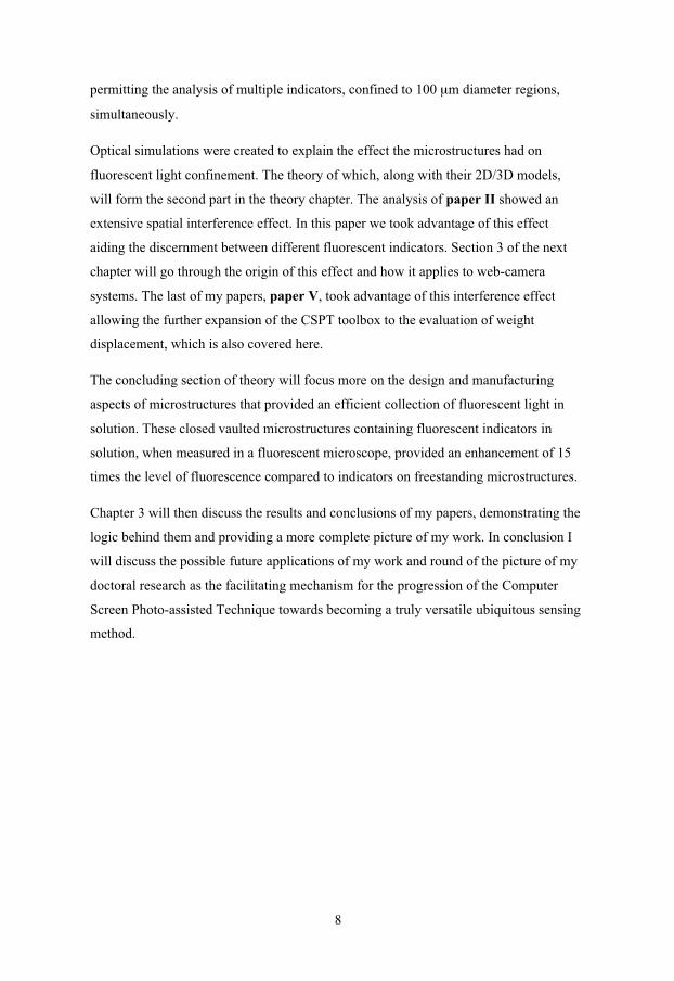
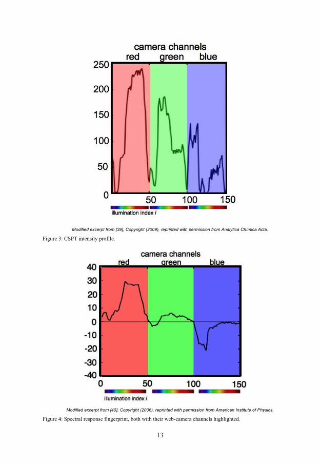
the images. It is from these that the intensity profiles for each illuminating colour,
unfolded in the three camera channels can be obtained. Figure 3 shows an example of
the concatenation of those intensity profiles. A CSPT fingerprint of a given ROI is then
constructed as the difference between an intensity profile for a target, such as fig. 3,
minus a reference intensity profile, an example of which is seen in figure 4.
A reference profile can take on many forms depending on the application. For the work
presented in this thesis the reference profile is obtained by measuring the spectral
fingerprint of an area where no other substances are present on the substrate. Other
methods include performing a pre-exposure fingerprint of a substance. Where here one
records the response of the substance pre-exposure to a reacting agent that, upon
exposure, will change the fingerprint response of the substance post-exposure [29, 37,
38].
13
Modified excerpt from [39], Copyright (2009), reprinted with permission from Analytica Chímica Acta.
Figure 3: CSPT intensity profile.
Modified excerpt from [40], Copyright (2006), reprinted with permission from American Institute of Physics.
Figure 4: Spectral response fingerprint, both with their web-camera channels highlighted.

14

15
PEEM: The polychromatic excitation emission
matrix
Spectral response fingerprinting can identify fluorescent indicators using the CSPT
platform. Numerous demonstrations and applications of this concept have been
described [16, 29, 30, 31]. However, at the beginning of my PhD the fingerprinting of
fluorescence substances was not well described and a model of the CSPT capable of
predicting such fingerprints was clearly missing. It was not fully understood how a
polychromatic light source and a tri-chromatic image detector could provide such
comparable spectral identification with spectroscopy.
Reprinted from [41], Copyright (2009), with permission from Analytica Chimica Acta.
Figure 5: (a) Spectral radiances of the 50 colours displayed on the computer screen. (b) Excitation
emission matrix of fluorescein. (c) Measured spectra under polychromatic illumination provided by the
computer screen. Ten spectra are highlighted using the corresponding colours used for illumination.
Black solid lines are the modelled spectra, which describe them as fingerprints of the EEM. The spectral
windows of the camera channels are also displayed with black lines. (d) CSPT fingerprint composed as
the concatenated intensity differences in the red, green and blue camera channels for all illuminating
colours. Open circles are the experimental result, with colours corresponding to illuminating colours and
the solid black lines are the modelled response.
16
The solution came with the realisation that the spectral response fingerprint was a
fingerprint of a polychromatically stimulated Excitation Emission Matrix (EEM). In
total spectroscopy the emission spectra of every excitation band is composed in a single
3D space, which produces a complete characterisation of a fluorescent sample [42, 43].
An example of one such contour plot for fluorescein is seen in figure 5 (b).
Usually a fluorescence spectrometer is used for EEM analysis. This instrument has a
broadband white light source and measures the emission of a fluorescent indicator for
each excitation wavelength. In our case, as I described in the previous section, a
computer screen illuminates with a polychromatic radiance ci(�) that can be varied for
each i index, figure 5 (a). When measuring fluorescence in a CSPT platform the
emission and transmission are entangled in the acquired fingerprints.
In contrast with standard spectroscopy, where the sample absorption is unique, in
CSPT, depending on the spectral radiance used for illumination, gaps in the excitation
can occur, figure 5 (a). In order to describe the transmittance measured with such a light
source we modulate the sample absorption (A(�)) with the particular radiance used for
illumination.
ai �( ) = c i �( )A �( ) (3)
where c i �( ) is the normalized screen spectral radiance and A(�) is the spectroscopic
absorption, with a transmittance:
� i = 10�ai �( )
(4)
Each illuminating colour is polychromatic and accordingly each measured emission
signal will be the result of multiple excitation lines. The result of this is that each
illumination probes a portion of the total EEM information of the fluorophore. If
� �, �em( ) is the normalized EEM of the substance, the CSPT emission
� i �em( ) can be
calculated as:
� i �em( ) = c i �( )
�
� � �, �em( )d� (5)

17
If we now calculate the total transmittance of a fluorescent sample under polychromatic
illumination we will get that the measurable signal � at a particular position x is
�i �, x( ) = n1 x( )� i �( ) + n2 x( )� i �em( )
(6)
where the weights n1 and n2 are variables that depend on the setup used for
measurement. This measurable signal can then be directly inserted into equation (2),
determining the intensity of pixels j in the red, green and blue channels of the web-
camera for fluorescence measurement eq. (2). It is these channels that are concatenated
to form the spectral fingerprints ( � i
j
) as in figure 3. Quite often a reference
subtraction is performed, as in figure 4, in order to highlight the fluorescent signal of
the sample and this results in a fingerprint:
� i
j
= � i
jsample
� � i
jref
(7)
Paper III formulates this theory and proves its plausibility by fitting the whole set of
PEEM’s for various substances using only two free parameters n1 and n2, figure 5 (d).
This result is further strengthened by the comparison of the PCA [44] evaluation pattern
using either traditional fluorescence spectroscopy or the CSPT platform and the above
model, where discrimination between different fluorescent substances is obtained to a
comparable level, figure 6 (a). Figure 6 (b) demonstrates the needed balance between
emission and excitation. The CSPT fingerprints being, this time, created from a purely
fluorescent signal. This results in a poor discrimination between the porphyrins, which
can be seen as the grouping together of their PCA scores. The results therefore show the
necessity to measure not just the excitation or emission profiles but a balanced
combination of the two.

18
Reprinted from [41], Copyright (2009), with permission from Analytica Chimica Acta.
Figure 6: (a) First two principal components score plot of the spectra (blue asterisk), CSPT fingerprints
(black squares) and modeled CSPT fingerprints (red diamonds) measured from a balance
excitation/emission region. (b) Idem to (a) but for a pure fluorescence region. Blue and black lines are a
help to the eye, highlighting the classification pattern.
19
Fluorescence and Prior Art
Fluorescence as a phenomenon is the result of an electron, being excited from the
ground state by a photon. The excited electron then decays down again to the ground
state by emitting its’ energy in the form of light [45]. Fluorescent indicators themselves
are used as labels in numerous types of assays [46] and as markers in fluorescent
microscopy [47]. In sensing applications these indicators can also be the functional
material by changing its optical characteristics after exposure to a target environment
[37]. The focus of my work has been on developing a technique to enhance the
detection of fluorescence signals in the context of CSPT detection.
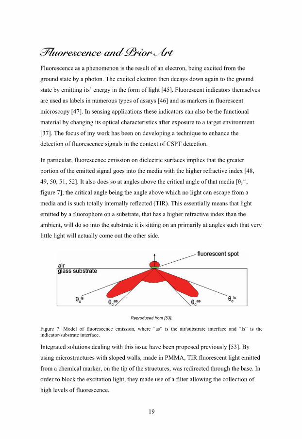
In particular, fluorescence emission on dielectric surfaces implies that the greater
portion of the emitted signal goes into the media with the higher refractive index [48,
49, 50, 51, 52]. It also does so at angles above the critical angle of that media [�cas
,
figure 7]; the critical angle being the angle above which no light can escape from a
media and is such totally internally reflected (TIR). This essentially means that light
emitted by a fluorophore on a substrate, that has a higher refractive index than the
ambient, will do so into the substrate it is sitting on an primarily at angles such that very
little light will actually come out the other side.
Reproduced from [53].
Figure 7: Model of fluorescence emission, where “as” is the air/substrate interface and “Is” is the
indicator/substrate interface.
Integrated solutions dealing with this issue have been proposed previously [53]. By
using microstructures with sloped walls, made in PMMA, TIR fluorescent light emitted
from a chemical marker, on the tip of the structures, was redirected through the base. In
order to block the excitation light, they made use of a filter allowing the collection of
high levels of fluorescence.

20
This is a drawback for our applications, since it requires the filter to be adapted for
different fluorophores, thereby limiting the versatility to sense diverse indicators. Also,
as was described in the previous section, the CSPT platform is dependant on a balance
of excitation and emission for its fingerprint evaluation and so we need to introduce
optical separation for this purpose.
We work with SU-8, which is a UV curable polymer having similar properties to glass.
This makes it a suitable element for our problem. By depositing it as a thin film on a
substrate and exposing it to UV light, microstructures of any shape can be generated
provided a suitable mask can be created [54, 55, 56, 57, 58, 59, 60]. These structures
thus provide multiple micro-testing areas and even the possibility to perform
microfluidics experiments [61].
21
SU-8 Microstructures
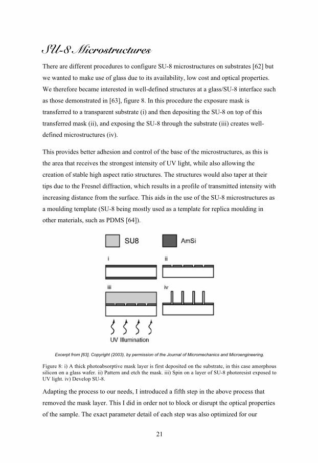
There are different procedures to configure SU-8 microstructures on substrates [62] but
we wanted to make use of glass due to its availability, low cost and optical properties.
We therefore became interested in well-defined structures at a glass/SU-8 interface such
as those demonstrated in [63], figure 8. In this procedure the exposure mask is
transferred to a transparent substrate (i) and then depositing the SU-8 on top of this
transferred mask (ii), and exposing the SU-8 through the substrate (iii) creates well-
defined microstructures (iv).
This provides better adhesion and control of the base of the microstructures, as this is
the area that receives the strongest intensity of UV light, while also allowing the
creation of stable high aspect ratio structures. The structures would also taper at their
tips due to the Fresnel diffraction, which results in a profile of transmitted intensity with
increasing distance from the surface. This aids in the use of the SU-8 microstructures as
a moulding template (SU-8 being mostly used as a template for replica moulding in
other materials, such as PDMS [64]).
Excerpt from [63], Copyright (2003), by permission of the Journal of Micromechanics and Microengineering.
Figure 8: i) A thick photoabsorptive mask layer is first deposited on the substrate, in this case amorphous
silicon on a glass wafer. ii) Pattern and etch the mask. iii) Spin on a layer of SU-8 photoresist exposed to
UV light. iv) Develop SU-8.
Adapting the process to our needs, I introduced a fifth step in the above process that
removed the mask layer. This I did in order not to block or disrupt the optical properties
of the sample. The exact parameter detail of each step was also optimized for our

22
patterns. This is because the quality of the final result is highly dependent on the exact
process conditions for particular layouts e.g. larger patterns with larger spacing develop
much quicker than patterns that are small and tightly packed. The specific recipes I used
for the generation of microstructures in papers I, II and IV can be found detailed in the
supplementary material section. Also, as can be read there, I did not use Amorphous
Silicon as a mask or glass wafers as a substrate, as in [63], instead choosing Chromium
as a mask and normal microscope slides as a substrate. Further modifications of this
fabrication process lead us to the monolithic roofed structures described at the end of
this chapter.
Paper 1: 2D Modelling
An optical model, using 2D and 3D raytracing software [65, 66], was developed to
examine the illumination of a SU-8 pillar arrayed microstructured substrate (figure 9).
Reprinted with permission from [40]. Copyright (2006), American Institute of Physics.
Figure 9: Left: Raytrace of light passing through a SU-8 microstructure. Right: Image of SU-8 hexagonal
microstructures on glass with a spot of fluorescein under cyan illumination.
The 2D raytracing showed that light incident, at an angle, on our substrate will be
refracted and conducted in two distinct directions. The majority of the light is
transmitted straight through but a small fraction will totally internally reflect (TIR) from
the microstructure wall and be directed towards the camera. It is this small fraction that
makes the structures visible even when the camera is not looking directly at the screen
through the structures, figure 9. This optical separation thereby allowing the selection of
a fraction of the transmitted signal.
To examine this behaviour with fluorescent substances a similar model was developed
but this time the focus was on fluorescent emission, figure 10. The emitted fluorescent

23
light is approximated here as point sources of light emitting above the critical angle of
the substrate it was resting on, which is the media with the higher refractive index [48]
(in this case the SU-8 microstructure or glass).
Due to the vertical walls light that is emitted at the critical angles of the SU-8, will
refract when passing into the glass substrate and change their dispersion angle in the
glass, escaping TIR. Meanwhile fluorescence, which is emitted from the tip of a
microstructure, will experience refraction through air before being refracted through the
substrate leading it to be collected by a web-camera perpendicular to the surface.
Reprinted with permission from [40]. Copyright (2006), American Institute of Physics.
Figure 10: Fluorescence emission model of fluorescent material on SU-8 and a glass substrate.
Paper 1: 3D Modelling
The above models were adequate to get a basic understanding of how SU-8
microstructures on a glass substrate can enhance fluorescent detection and provide
optical separation. However, they can’t visualise what occurs when microstructures of
different shapes and spacings are illuminated and how the 3D optical light paths will
develop through a glass substrate. Therefore a 3D raytracing model was developed.
Here light rays could be visualised and the effect of objects on their light paths
modelled. Two models were thus generated that contained to-scale representations of
the groups of SU-8 pillars used in paper I, i.e. hexagonal and circular.
The microstructured areas were essentially a bound repetition of a smaller scale pattern.
Therefore the model contains just a small group of structures at the four corners of the
microstructured areas. This provides the boundary limits of how light would be affected
by passing through a glass substrate with microstructured elements, with all other light
effects contained within these limits.
24
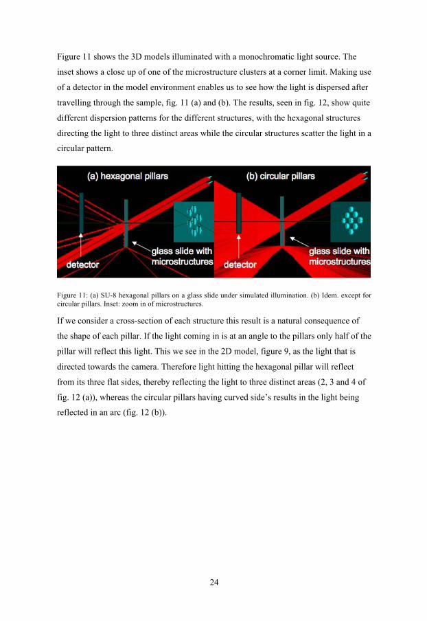
Figure 11 shows the 3D models illuminated with a monochromatic light source. The
inset shows a close up of one of the microstructure clusters at a corner limit. Making use
of a detector in the model environment enables us to see how the light is dispersed after
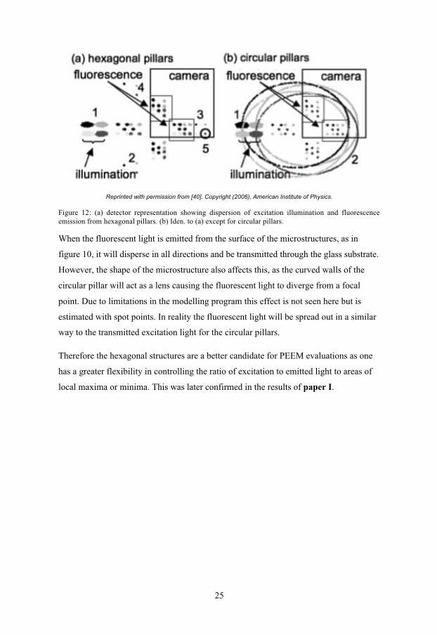
travelling through the sample, fig. 11 (a) and (b). The results, seen in fig. 12, show quite
different dispersion patterns for the different structures, with the hexagonal structures
directing the light to three distinct areas while the circular structures scatter the light in a
circular pattern.
Figure 11: (a) SU-8 hexagonal pillars on a glass slide under simulated illumination. (b) Idem. except for
circular pillars. Inset: zoom in of microstructures.
If we consider a cross-section of each structure this result is a natural consequence of
the shape of each pillar. If the light coming in is at an angle to the pillars only half of the
pillar will reflect this light. This we see in the 2D model, figure 9, as the light that is
directed towards the camera. Therefore light hitting the hexagonal pillar will reflect
from its three flat sides, thereby reflecting the light to three distinct areas (2, 3 and 4 of
fig. 12 (a)), whereas the circular pillars having curved side’s results in the light being
reflected in an arc (fig. 12 (b)).
25
Reprinted with permission from [40]. Copyright (2006), American Institute of Physics.
Figure 12: (a) detector representation showing dispersion of excitation illumination and fluorescence
emission from hexagonal pillars. (b) Iden. to (a) except for circular pillars.
When the fluorescent light is emitted from the surface of the microstructures, as in
figure 10, it will disperse in all directions and be transmitted through the glass substrate.
However, the shape of the microstructure also affects this, as the curved walls of the
circular pillar will act as a lens causing the fluorescent light to diverge from a focal
point. Due to limitations in the modelling program this effect is not seen here but is
estimated with spot points. In reality the fluorescent light will be spread out in a similar
way to the transmitted excitation light for the circular pillars.
Therefore the hexagonal structures are a better candidate for PEEM evaluations as one
has a greater flexibility in controlling the ratio of excitation to emitted light to areas of
local maxima or minima. This was later confirmed in the results of paper I.
26
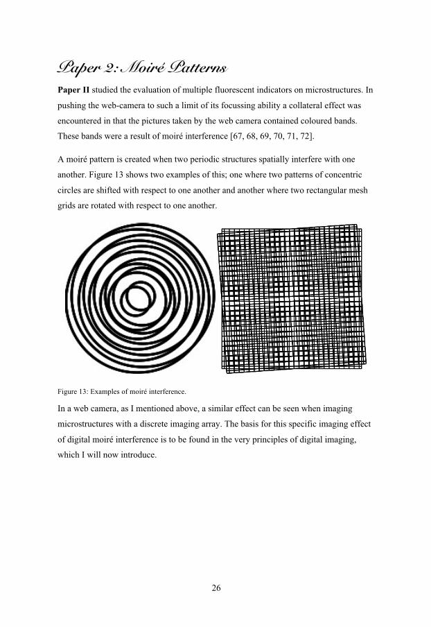
Paper 2: Moiré Patterns
Paper II studied the evaluation of multiple fluorescent indicators on microstructures. In
pushing the web-camera to such a limit of its focussing ability a collateral effect was
encountered in that the pictures taken by the web camera contained coloured bands.
These bands were a result of moiré interference [67, 68, 69, 70, 71, 72].
A moiré pattern is created when two periodic structures spatially interfere with one
another. Figure 13 shows two examples of this; one where two patterns of concentric
circles are shifted with respect to one another and another where two rectangular mesh
grids are rotated with respect to one another.
Figure 13: Examples of moiré interference.
In a web camera, as I mentioned above, a similar effect can be seen when imaging
microstructures with a discrete imaging array. The basis for this specific imaging effect
of digital moiré interference is to be found in the very principles of digital imaging,
which I will now introduce.
27
Digital Imaging
On the market today are two main types of digital image recorders: Charged Coupled
Devices (CCD) and Complementary Metal Oxide Semiconductor (CMOS) devices.
They both detect photons and transform this analogue signal into a digital one, but in
slightly different ways [73]. However they function under the same principle; light hits
a photosensitive cell or pixel which, in the case of a 24-bit colour detector, outputs a
signal with a resolution of 0 – 255 intensity values per channel. As I described
previously in “PEEM: Fingerprints” the photosensitive cells are covered in three types
of filters. The pattern in which they cover the cells is known as a Bayer pattern [74] and
separates the detector into three channels representing each of these colours, with twice
as many green pixels as red and blue (mimicking the sensitivity of human vision). This
is a way of minimizing cost and size of the detector by only needing one multi-filtered
detector instead of three individually filtered ones. The output signal from the various
pixels is then associated with its respective colour filter.
It is this intensity value and coloured grid position that results in what is called a Bayer
image. If we now consider a simple object like that of figure 14 (a) and point a colour
digital image detector at this object, figure 14 (b). We will produce a Bayer image as in
figure 14 (c), which will then be subsequently sent to the detector processor. Due to the
cost-saving channel separation of the Bayer filter, the red and blue channels contain the
intensity information for one quarter of the image each while the green channel contains
half of the intensity information.
Further processing is now performed called demosaicing [75]. This process can be done
using a number of different mathematical methods [76, 77]. The simplest and quickest
of which is bilinear interpolation.

28
Figure 14: (a) original image. (b) Bayer filter. (c) Channel decomposition of the indicated area of (a). (d) Digital
image.
Bilinear interpolation is a process that takes the average of the pixel intensity
surrounding unknown values in a specific channel and assigns this average value to
them.
Figure 15: Bayer filter representation with numbered pixels.
The same approach is then applied to the unknown pixel intensities of the blue and
green channels. After this process is completed the final image is then composed of
these three layers of the interpolated red, green and blue channels, which when
combined together reproduces a digital image of the initial object, figure 14 (d).

29
Moiré And The CSPT Platform
The previous method works very well in most cases and with regard to a web-camera,
whose primary area of use is in imaging faces and rudimentary shapes, this method is
very effective and cheap. However, when we now try to use these devices outside of
their normal realm of use, as in imaging microstructures, it gives rise to a moiré pattern.
In paper II 100 μm hexagonal SU-8 microstructures on glass were imaged through a
web-camera under computer screen illumination. The web-camera was placed at a
distance of 1 cm from the structured substrate. However, even at this short distance the
resolution of the camera was insufficient to prevent a moiré pattern appearing on the
digitised image of the microstructures, figure 16.
By changing the distance between the camera and the microstructures the projection of
the image on the detector changes, thus generating different moiré patterns that
highlight different regions of the Bayer filter. Thereby enabling the Bayer information
to be decoded in the demosiced image. This relationship of distance and moiré bands is
one widely used in industry for positioning [78, 79, 80] and is even used for touch
screen technology [81]. Paper V takes advantage of this effect by using the difference
between two imaged moiré bands to infer a change in weight.
Reprinted with permission from [39]. Copyright (2009), Analytica Chímica Acta.
Figure 16: Image of microstructures under white illumination with the deposition areas indicated 1. Old Rhodamine,
2. Old Fluorescein, 3. Ge-Tcp, 4.Zn-Tpp, 5. Rhodamine, 6-8 Fluoresceins and an illustration of the pixels selected for analysis in the areas 4 and 8 is shown to the side.

30
Paper 2: Bayer Image Fingerprinting
There is though an advantage to this effect in that we now have access to a Bayer like
image. Ideally, one would always want to use the un-demosiced Bayer image for
spectral analysis. This is because due to the interpolation done to obtain the demosaiced
image, a lot of averaging is performed, which degrades the acquired spectral
information. This is disadvantageous for analysis purposes, as you would want to retain
as much of the pure original signal as possible. The Bayer image can be accessed
through a dedicated driver or directly produced by digital imaging. So as the CSPT
platform is considered to be a ubiquitous user-friendly platform, being able to access
Bayer like information without modifying the setup will greatly increase the
functionality of the platform.
Returning now to the issue of fluorescent fingerprinting on microstructures, we find
ourselves in a situation whereby information of the Bayer pattern is overlaid on the final
image. Recalling from previously, a spectral fingerprint is composed of the
concatenated intensity values from the three camera channels in a specified ROI. If we
were to use this method to try to evaluate a fluorescent indicator on a single
microstructure in figure 16, discrimination would be very poor as the sample will sit on
either a red, green or blue Bayer region. The chosen configuration in paper II resulted
in mostly red or blue regions only.
A new spectral fingerprint evaluation procedure was subsequently developed to take
advantage of this new information and in paper II discrimination between two different
fluorescent indicators and two porphyrins as well as discrimination between newer and
older depositions of the same indicators was achieved. All of which had been deposited
on groups of individual 100 μm hexagonal microstructures, figure 16.
The new method involved extracting similar information from individual pixels within
each ROI, which consisted of the groups of similarly coated micropillars as indicated in
figure 16. As before the area was illuminated with a sequence of 50 colours from a
computer screen. To extract and group the pixels that had similar spectral responses in
each ROI a PCA of all the pixels in a ROI was plotted, figure 17.

31
Reprinted with permission from [39]. Copyright (2009), Analytica Chímica Acta.
Figure 17: PCA of all the pixels contained with ROI 1 of figure 16.
This process of selection was performed on image 16 as under white illumination it is
easier to discriminate between red and blue pillars as well as ensuring that the pixel
selection is performed correctly. As can be seen in figure 17 a large proportion of the
image is black (representing the black background) and then as you move to the right of
the plot a clear division between blue and red coloured pillars is seen. By selecting two
sets in this plot that exhibit similar spectral responses it becomes possible to choose the
pixels that provide the best fluorescent signals discriminated in the two decoded Bayer
regions.
By combining the spectral fingerprints of red and blue Bayer regions into a single
spectral fingerprint for each substance, one can naturally exploit the Bayer decoding,
thus improving the discrimination between indicators. Figure 18 is an example of one
such combination.

32
Reprinted with permission from [39]. Copyright (2009), Analytica Chímica Acta.
Figure 18: Spectral fingerprint of one red and one blue pixel from ROI 1.
By collecting together 50 such red/blue pixels pairs for each ROI and normalizing to
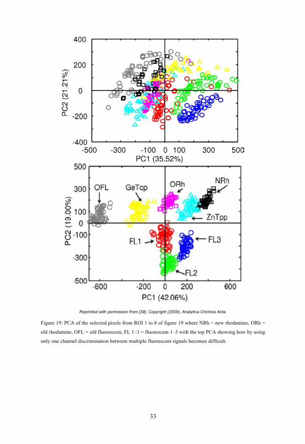
reduce noise it is possible to discriminate between all regions. In figure 19 it is even
possible to see a difference in fluorescent signal between older and more recently
deposited indicators, with older indicators having more quenched emissions and thereby
represented here as a tendency to drift left in the PCA. If one attempts to discriminate
the same amount of information but by using just one of the above sets the top PCA of
figure 19 shows that discrimination then becomes more difficult, further supporting the
benefits of Bayer decoding.
33
Reprinted with permission from [39]. Copyright (2009), Analytica Chímica Acta.
Figure 19: PCA of the selected pixels from ROI 1 to 8 of figure 19 where NRh = new rhodamine, ORh =
old rhodamine, OFL = old fluorescein, FL 1–3 = fluorescein 1–3 with the top PCA showing how by using
only one channel discrimination between multiple fluorescent signals becomes difficult.
34
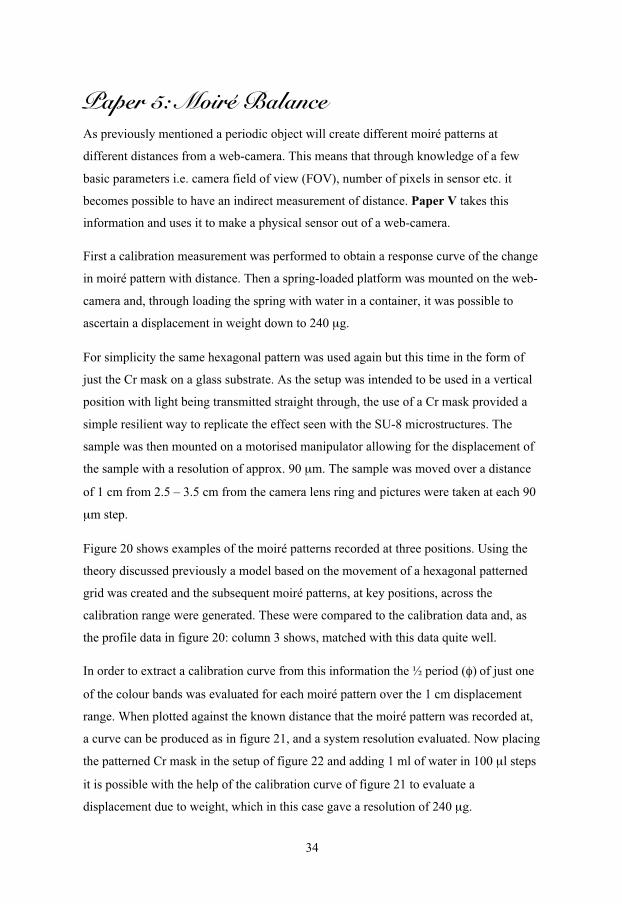
Paper 5: Moiré Balance
As previously mentioned a periodic object will create different moiré patterns at
different distances from a web-camera. This means that through knowledge of a few
basic parameters i.e. camera field of view (FOV), number of pixels in sensor etc. it
becomes possible to have an indirect measurement of distance. Paper V takes this
information and uses it to make a physical sensor out of a web-camera.
First a calibration measurement was performed to obtain a response curve of the change
in moiré pattern with distance. Then a spring-loaded platform was mounted on the web-
camera and, through loading the spring with water in a container, it was possible to
ascertain a displacement in weight down to 240 μg.
For simplicity the same hexagonal pattern was used again but this time in the form of
just the Cr mask on a glass substrate. As the setup was intended to be used in a vertical
position with light being transmitted straight through, the use of a Cr mask provided a
simple resilient way to replicate the effect seen with the SU-8 microstructures. The
sample was then mounted on a motorised manipulator allowing for the displacement of
the sample with a resolution of approx. 90 μm. The sample was moved over a distance
of 1 cm from 2.5 – 3.5 cm from the camera lens ring and pictures were taken at each 90
μm step.
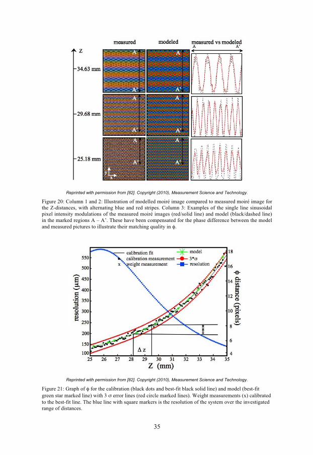
Figure 20 shows examples of the moiré patterns recorded at three positions. Using the
theory discussed previously a model based on the movement of a hexagonal patterned
grid was created and the subsequent moiré patterns, at key positions, across the
calibration range were generated. These were compared to the calibration data and, as
the profile data in figure 20: column 3 shows, matched with this data quite well.
In order to extract a calibration curve from this information the � period (�) of just one
of the colour bands was evaluated for each moiré pattern over the 1 cm displacement
range. When plotted against the known distance that the moiré pattern was recorded at,
a curve can be produced as in figure 21, and a system resolution evaluated. Now placing
the patterned Cr mask in the setup of figure 22 and adding 1 ml of water in 100 μl steps
it is possible with the help of the calibration curve of figure 21 to evaluate a
displacement due to weight, which in this case gave a resolution of 240 μg.
35
Reprinted with permission from [82]. Copyright (2010), Measurement Science and Technology.
Figure 20: Column 1 and 2: Illustration of modelled moiré image compared to measured moiré image for
the Z-distances, with alternating blue and red stripes. Column 3: Examples of the single line sinusoidal
pixel intensity modulations of the measured moiré images (red/solid line) and model (black/dashed line)
in the marked regions A – A’. These have been compensated for the phase difference between the model
and measured pictures to illustrate their matching quality in �.
Reprinted with permission from [82]. Copyright (2010), Measurement Science and Technology.
Figure 21: Graph of � for the calibration (black dots and best-fit black solid line) and model (best-fit
green star marked line) with 3 � error lines (red circle marked lines). Weight measurements (x) calibrated
to the best-fit line. The blue line with square markers is the resolution of the system over the investigated
range of distances.

36
Reprinted with permission from [82]. Copyright (2010), Measurement Science and Technology.
Figure 22: Setup for measurement of weight displacement due to moiré pattern shifting in digital images
of a Cr patterned glass substrate.

37
Roofed Microstructures
This final section of this chapter will discuss a method to create monolithic 3D
microstructures in SU-8.
As light passes through an aperture it will be diffracted, with a greater diffraction effect
being seen as the wavelength of the light approaches the size of the aperture. In our SU-
8 microstructure manufacturing process holes as small as 30 μm are used to create
structures of such a diameter. As we are using an ultra violet light source with
wavelengths around 375 nm a noticeable diffraction effect is present.
This is seen and commented on in [63] as a tapering of the tips of the microstructures
and a firm attachment in the base of the structure. In our work we use the diffraction
pattern along the 30 μm thick SU-8 film, which is being illuminated from the aperture
(mask) at the glass/SU-8 interface to the SU-8 surface. By playing with the shape and
the coordination of the aperture (mask pattern) we can control the 3D profile of the
illuminating pattern and even have a higher intensity in the distal region of the polymer.
This strategy allows us to cross-link the polymer at the distal surface while providing
empty inner spaces of controlled geometry (paper IV).
Following the manufacturing procedure in the second section of the supplementary
material, by exposing SU-8 through a mask that it is in intimate contact with over a
range of intensities from 180 – 252 mJ cm-2
, one can produce cavities of various forms.
Figure 23 shows a simplified model of this process for a single aperture, with figure 23
(b) illustrating the intensity profile distribution from an aperture of the same size as in
(a).

38
Reprinted with permission [83], Copyright (2009), from Micromechanics and Microengineering.
Figure 23: (a) Scheme of a mask feature of the width b under the experimental conditions used for SU-8
exposure. (b) Diffraction profiles at different distances from the substrate. (c) Model of cross-linking of
the SU-8 due to the Fresnel diffraction from two adjacent mask apertures.
This intensity distribution Iz after passing through the aperture is calculated from [84],
IZ =
I0
4C u2( ) �C u1( )[ ]
2
+ S u2( ) � S u1( )[ ]2�
� �
� �
(8)
where C(u) and S(u) are the Fresnel integrals;
C u( ) = cos �u�2 / 2( )du�
0
u� and
S u( ) = sin �u�2 / 2( )du�
0
u� , (9)
with

39
u = b
2
2
� • z (10)
at a distance z (0 - 30 μm) from the aperture and a aperture width b, using a wavelength
� in this case of 365 nm.
Figure 23 (c) shows the cross-linking profile achievable between two adjacent apertures
when the photon energy is increased above 170 mJ cm-2
for 30 μm thick SU-8, thus
creating cavities in the non-crosslinked areas. Three such cavity structures created using
square, hexagonal and circular apertures at different photon energies are shown in figure
24: column 1. To better understand the 2D distribution of the diffracted UV light that
created these cavity structures, a Matlab model for 2D Fresnel diffraction [85] figure
24: column 3 was made.
This time the output 2D diffraction profile is based on the convolution of an input wave
and an aperture structure, which according to Fourier optics in [85]
�p x, y,z( ) = �p0
x, y( )� h x, y,z( ) (11)
where z is 0 - 30 μm as before and,
h x, y,z( ) = e
jk 0 z� j �
k0
2�z� e
� j�k 0 x 2 + y 2( )
2 z (12)
with k0 = 365 nm.
Clearly seen in the simulation is the degree of overlapping that emanates from the edges
of all the apertures. It is this overlap that provides the required photon energy to cross-
link the SU-8 in the tips of the structures while leaving the area around the bases free.
In order to test the cavity structures a roofed microstructure based on circular pillars,
figure 25, was filled with a solution of rhodamine B. These structures were then able to
collect a fluorescent signal 15 times larger than the corresponding open (not roofed)
structures.
40
Reprinted with permission [83], Copyright (2009), from Micromechanics and Microengineering.
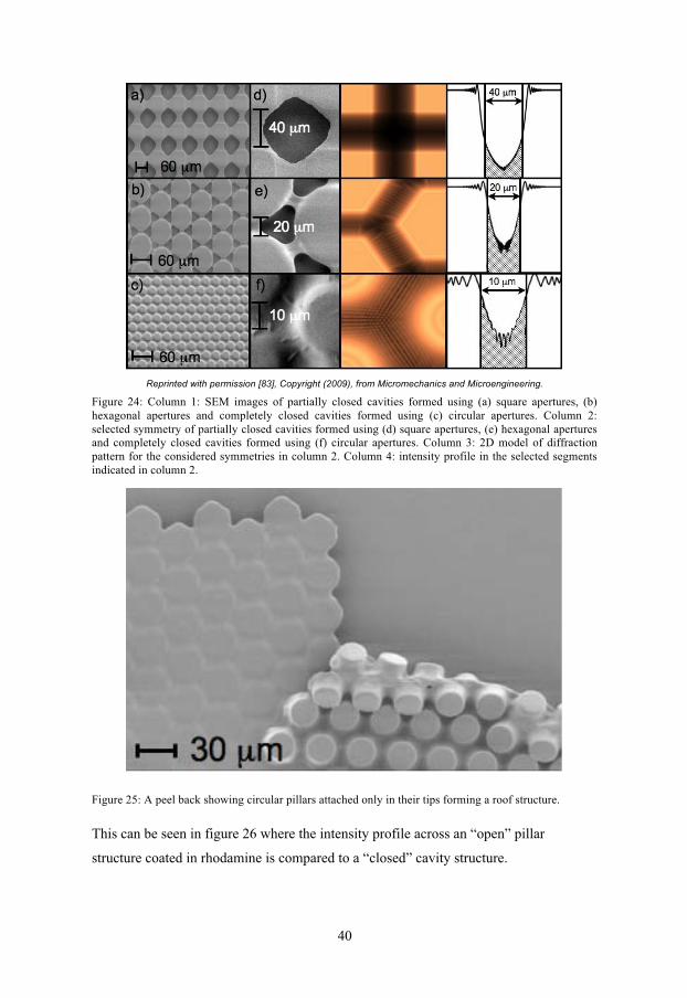
Figure 24: Column 1: SEM images of partially closed cavities formed using (a) square apertures, (b)
hexagonal apertures and completely closed cavities formed using (c) circular apertures. Column 2:
selected symmetry of partially closed cavities formed using (d) square apertures, (e) hexagonal apertures
and completely closed cavities formed using (f) circular apertures. Column 3: 2D model of diffraction
pattern for the considered symmetries in column 2. Column 4: intensity profile in the selected segments
indicated in column 2.
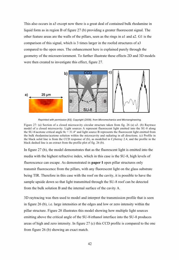
Figure 25: A peel back showing circular pillars attached only in their tips forming a roof structure.
This can be seen in figure 26 where the intensity profile across an “open” pillar
structure coated in rhodamine is compared to a “closed” cavity structure.

41
Reprinted with permission [83], Copyright (2009), from Micromechanics and Microengineering.
Figure 26: (a) 0.5 mM rhodamine on 25 μm wide and 30 μm tall: (a1) open circular pillars, (a2) open
circular pillars with a mirror in the back and (a3) closed circular structures with embedded Cr mirror. (b)
Profiles taken from indicated white line, across (a1) and (a3), comparing fluorescent signal in the green
channel for open (dashed black line) and closed (solid black line), circular patterned SU-8.
If we look over the distance B – B’ in each picture a1 – a3, two distinct features can be
compared between the open structures and the roofed ones. The first of these is the
signal in the distance between adjacent pillars. Comparing the opened structures to the
roofed one, G2, sees a 15 fold increase in the detected fluorescence. This is the signal
from the bulk rhodamine that is contained within the cavities of the roofed structured.
As explained previously fluorescence near a dielectric is emitted above the critical angle
of the dielectric leading to poor transmission. This is the result we see in a1 and a2.
42
This also occurs in a3 except now there is a great deal of contained bulk rhodamine in
liquid form as in region B of figure 27 (b) providing a greater fluorescent signal. The
other feature areas are the walls of the pillars, seen as the rings in a1 and a2. G1 is the
comparison of this signal, which is 3 times larger in the roofed structures of a3
compared to the open ones. The enhancement here is explained purely through the
geometry of the microenviornment. To further illustrate these effects 2D and 3D models
were then created to investigate this effect, figure 27.
Reprinted with permission [83], Copyright (2009), from Micromechanics and Microengineering.
Figure 27: (a) Section of a closed microcavity circular structure taken from fig. 26 (a) a3. (b) Raytrace
model of a closed microcavity. Light sources A represent fluorescent light emitted into the SU-8 along
the SU-8/acetone critical angle �c = 31.4° and light source B represents the fluorescent light emitted from
the bulk rhodamine/acetone solution within the microcavity and radiating in all directions. (c) Profile in
the black solid line is from the CCD response of (b), as modelled in Cyberray 2.4, and the profile in the
black dashed line is an extract from the profile plot of fig. 26 (b).
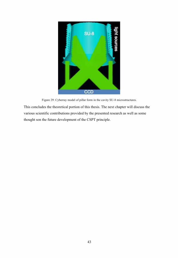
In figure 27 (b), the model demonstrates that as the fluorescent light is emitted into the
media with the highest refractive index, which in this case is the SU-8, high levels of
fluorescence can escape. As demonstrated in paper I open pillar structures only
transmit fluorescence from the pillars, with any fluorescent light on the glass substrate
being TIR. Therefore in this case with the roof on the cavity, it is possible to have the
sample upside down so that light transmitted through the SU-8 roof can be detected
from the bulk solution B and the internal surface of the cavity A.
3D raytracing was then used to model and interpret the transmission profile that is seen
in figure 26 (b), i.e. large intensities at the edges and low or zero intensity within the
pillar structure. Figure 28 illustrates this model showing how multiple light sources
emitting above the critical angle of the SU-8/ethanol interface into the SU-8 produces
areas of high and zero intensity. In figure 27 (c) this CCD profile is compared to the one
from figure 26 (b) showing an exact match.
43
Figure 29: Cyberray model of pillar form in the cavity SU-8 microstructures.
This concludes the theoretical portion of this thesis. The next chapter will discuss the
various scientific contributions provided by the presented research as well as some
thought son the future development of the CSPT principle.

44

45
Chapter 3: Drawing to a close
Concluding remarks and discussions around the contributions of this work.

46

47
PPaper 1
The CSPT platform is a collection point for optical techniques. Instead of having
diverse instruments that have a few specific functions the CSPT platform has an
adaptability that allows it to adopt optical techniques for analysis in the visual spectrum.
By taking microstructures that are normally used for microfluidics in lab-on-a-chip
applications I developed a method that allowed for a significant increase in fluorescence
detection in the CSPT platform. Looking to the final results, shown here in figure 30,
the introduction of a microstructured substrate increased fluorescent signals by a factor
of 5 and 3.16 for hexagonal and circular pillars respectively.
Reprinted with permission from [40]. Copyright (2006), American Institute of Physics.
Figure 30: (a) CSPT spectral fingerprints of fluorescein deposited on hexagonal pillars for illuminating
angles from (�) 6° to 40°. The inset shows a 4 mm area of pillars illuminated with a cyan colour. The
white circles indicate the regions of interest selected to compose the fingerprints. The dark frame of the
inset is the image of the glass surface without pillars. (b) Idem as (a) but for circular pillars.
The angle of the sample to the screen was varied during this experiment in order to find
the best balance in the PEEM. This occurs at 40° as this is the point beyond which light
will start to enter directly into the camera and cause too much background illumination
thereby disrupting the PEEM balance and leading to poorer signals. For comparison a
spot of fluorescent material was deposited on bare glass and measured in the same way
at the various angles. The black dashed line is the result of this and remains low and
constant throughout, demonstrating the clear advantage of the SU-8 microstructures.
This paper was the first use of micro pillar arrays to provide simple, flexible and
compact optical separation compatible with PEEM. This development furthermore

48
introduced a more sophisticated alternative to CSPT experiments and was an essential
step towards more advanced detections.
PPaper 2
Continuing on from the work of paper I this paper took the detection of fluorescent
material to the next logical phase i.e. the detection and discrimination between multiple
indicators simultaneously. As discussed in Ch. 2 this process provided us with a number
of challenges, with the eventual development of an adaption of the fingerprinting
process to exploit the presence of moiré fringes. Interestingly these fringes were present
in the first paper however they were removed simply through defocusing the lens
slightly. At this 1 cm distance from the web-camera the fringes can be easily removed
using this technique without any great loss in resolution. It is only when, as in this
paper, we wished to have individual pillar resolution that a sharp focus was needed and
thus required the development of the new evaluation process.
Paper 3
This paper, which was developed alongside the previous two, forms the backbone of the
whole fluorescent detection theory on the CSPT platform. By showing that a spectral
fingerprint captures the excitation emission matrix associated to a fluorescent indicator,
a consistent explanation to the identification capabilities seen in the first two papers was
developed. This also showed for the first time that the CSPT platform is supported by a
robust detection concept on par with those used in more advanced instrumentation.
Paper 4
Normally when working with microstructures their main purpose is to be used in
combination with microchannels in a micro-fluidic system. It is therefore crucial that
the system be completely sealed before any liquid is sent through. This is usually
achieved through creating the channels and microstructures on one substrate and then
attaching a separate roof piece using some form of sealant. This is a very sensitive
procedure as the channels could become filled with sealant or an incomplete seal could
be made such that the system leaks when filled with liquid.

49
If instead one creates a micro-fluidic system that has a roof already, much time, cost
and resources can be saved. By exposing SU-8 beyond its recommended dosage, and
using controlled diffraction, it becomes possible to create vaulted cavities with a roof in
just one exposure step. What was often considered something to be avoided now
becomes a very useful method for the fast production of lab-on-a-chip devices.
PPaper 5
The last of my papers to be published showed the versatility of the CSPT platform by
demonstrating the use of a web-camera as a weight displacement sensor. This work
constitutes a first explanation of the CSPT concept outside the chemical sensing field
and extends its applicability to physical parameters (such as weight or distance), which
can have important complementary uses aside from its main use as a chemical sensor. It
was also while working on this paper that the full model of moiré fringe generation was
developed, providing a testing platform for the development of other patterns for fringe
analysis at shorter or farther distances.

50
51
Outlook
The future of any research is always hard to predict as there are so many variables that
can affect its development. From grant money, to manpower, to availability of resources
all these things guide and shape all scientific research. However a good guess can be
made and for the CSPT platform to evolve further a jump to mobile phone technology is
the next obvious step. With their availability and increasing complexity mobile phones
are more and more like mini computers with built in cameras, thus making them ideal
for the CSPT concept. The first demonstration of this is [86], where we have shown
how a standard medical test can be evaluated with the aid of a just a mobile phone.
Other possibilities are open now due to my last paper allowing the CSPT platform to
explore physical sensing. Moiré interference can be induced in a web-camera using any
type of high contrast periodic structure so monitoring the movement of flexible micro-
pillars can provide e.g. flow measurements. Rhythmic patterns of movement like
breathing could even be monitored using this technique. Where the movement to be
monitored is transduced into movement in a camera with respect to a fixed pattern.
The true beauty with the CSPT technology is its accessibility and connectivity. By using
everyday electronics and simple sample interfaces the measurement of chemical
substances can be performed by any layperson in similar ways to pregnancy tests or
urine tests today. This will most likely lead to its usage in hereto-untried fields like
botany for examining and recording new species to criminal forensics for on the spot
analysis of crime scene evidence.
It is easy to see the progress towards more mobile versions of the CSPT platform, as I
mentioned above, but as a stationary and easily managed measurement tool it also has
the possibility of being used for environmental monitoring. By placing CSPT platforms
at key points of interest and with the possibility to connect to the Internet, CSPT
measurements could be geo-tagged, providing fast and accurate analysis of e.g. the
water quality throughout an entire river system or the spread of an air-born virus
throughout an entire building.

52

53
Supplementary Material
SU-8: Microstructure generation paper 1 and 2
SU-8 is an epoxy resin that contains a photosensitive cationic salt. When this salt is
exposed to UV radiation, between 350 - 400 nm, it becomes a powerful acid. This in
turn will cause the SU-8 resin to cross-link its’ molecules when heated [87], thereby
leaving hardened SU-8 resin. This hardened resin is resistant to developing agents thus
allowing the removal un-exposed regions [88] and making SU-8 a negative-tone
photoresist.
SU-8 can also be purchased in various viscosities. This is for the convenience of the end
user as the diluter of SU-8 is fairly toxic. For all of the work presented here SU-8 (10)
was used, which can provide structures approximately 30 μm high. This we chose
merely out of convenience as SU-8 with higher viscosity gives very thick layers that
require a much longer process time [60] and lower viscosity SU-8 will only create very
small structures [88], which was not helpful for us as we needed something large
enough for optical testing. What follows is the procedure I developed for creation of 30
μm high microstructures with various shapes and spacing.
Standard microscope glass slides were cleaned in H2O : H2O2 : HCl (6:1:1) for 10 mins
to remove any residue and provide a good surface for SU-8 attachment. After drying
with N2 gas, 150 nm of Cr were deposited through thermal evaporation, from tungsten
boats, onto one side of the slides.
Cr films were then coated with S1818 by spin on a disk at 4000 rpm for 30 sec. Directly
after spinning the samples were baked at 100°C for 1 min before being exposed for 10
sec at 3.6 mJ cm-2
by a UV mask aligner system, through a patterned quartz mask. After
development the exposed Cr, after the removal of S1818, was etched using a wet-
etching chemical process resulting in the dissolution of the exposed Cr film. Washing
with acetone and water to remove the un-exposed S1818 gave a Cr patterned glass slide,
which could then be used as a mask for SU-8 micro-fabrication.
When the samples were thoroughly dried a layer of SU-8 (10) was spun onto the slide
by first spinning at 500 rpm for 15 sec and then at 1000 rpm for 30 sec. This two-step
54
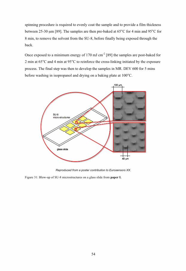
spinning procedure is required to evenly coat the sample and to provide a film thickness
between 25-30 μm [89]. The samples are then pre-baked at 65°C for 4 min and 95°C for
8 min, to remove the solvent from the SU-8, before finally being exposed through the
back.
Once exposed to a minimum energy of 170 mJ cm-2
[89] the samples are post-baked for
2 min at 65°C and 4 min at 95°C to reinforce the cross-linking initiated by the exposure
process. The final step was then to develop the samples in MR. DEV 600 for 5 mins
before washing in isopropanol and drying on a baking plate at 100°C.
Reproduced from a poster contribution to Eurosensors XX.
Figure 31: Blow-up of SU-8 microstructures on a glass slide from paper I.

55
SU-8: Microstructure generation paper 4
Figure 32: Enclosed microstructures from paper IV.
As stated before, for a depth of 30 μm a minimum exposure of 170 mJ cm�2
is required
to cross-link the SU-8. However, this dosage is used to cross-link the directly exposed
SU-8 and not the area in between the mask features where the intensity is much lower.
Also the manufacture of SU-8 microstructures is a many stepped process and each step
has an influence on the final result i.e. the length of time spent developing the
structures, the spacing between mask features, as well as the pre/post exposure baking
conditions. Therefore, in order to produce microcavities a specific set of process
parameters must be found.
Pre/post exposure baking conditions provide stability to the structure and ensure that the
SU-8 roofs cross-link, which has been shown for the bulk SU-8 elsewhere [90]. A two-
step baking procedure, where the pre-baking conditions were to eliminate the solvent in
the SU-8 and the post-baking conditions were to selectively cross-link the exposed SU-
8 [89], was used: 4min at 65 °C and 8min at 95 °C pre-baking / 2 min at 65 °C and 4
min at 95 °C post-baking. Also due to the weak exposure of the roofs, it was found that
excessively long development could almost completely remove the roof structure.
Therefore a 5 min development time with an isopropanol wash at 2.5 min was
considered optimal.
As expected, similar mask features with different spacing’s could form a cap at different
exposure times. For example, a mask feature with a spacing of 30 μm formed roofs with
252 mJ cm�2
, with a spacing of 20 μm roof formation occurred with 216 mJ cm�2
and
with a spacing of 10 μm roof formation occurred with 180 mJ cm�2
.

56
Figure 33: Column 1: SEM images of partially closed cavities formed using (a) square apertures, (b)
hexagonal apertures and completely closed cavities formed using (c) circular apertures. Column 2:
selected symmetry of partially closed cavities formed using (d) square apertures (e) hexagonal apertures
and completely closed cavities formed using (f) circular apertures.
This sections text and figures reprinted from [83], Copyright (2009), with permission from Micromechanics
and Microengineerin

57
Bibliography:
[1] J. Reimer, "Personal Computer Market Share: 1975-2004", Ars Technica (December
2005), http://arstechnica.com/old/content/2005/12/total-share.ars.
[2] R. A. Potyrailo, W. G. Morris, A. M. Leach, T. M. Sivavec, M. B. Wisnudel, and S.
Boyette, “Analog signal acquisition from computer optical disk drives for quantitative
chemical sensing”, Anal. Chem. 78 (2006), pg. 5893 – 5899.
[3] R. A. Potyrailo, W. G. Morris, A. M. Leach, L. Hassib, K. Krishnan, C. Surman, R.
Wroczynski, S. Boyette, C. Xiao, P. Shrikhande, A. Agree and T. Cecconie, “Theory
and practice of ubiquitous quantitative chemical analysis using conventional computer
optical disk drives”, App. Opt. vol. 46, no. 28 (2007), pg. 7007 – 7017.
[4] R. A. Potyrailo, W. G. Morris, R. Wroczynski, L. Hassib, P. Miller, B. Dworken, A.
M. Leach, S. Boyette, C. Xiao, “Multi-wavelength operation of optical disk drives for
chemical and biological analysis”, Sens. Act. B 136 (2009), pg. 203 – 208.
[5] N. A. Rakow and K. S. Suslick, “A colorimetric sensor array for odour
visualization”, Nature, 406 (2000), pg 710 – 712.
[6] K. S. Suslick, N. A. Rakow and A. Sen, “Colorimetric sensor arrays for molecular
recognition”, Tetrahedron, 60 (2004), pg. 11133 – 11138.
[7] N. A. Rakow, A. Sen, M. C. Janzen, J. B. Ponder, and K. S. Suslick, “Molecular
recognition and discrimination of amines with a colorimetric array”, Angew. Chem. Int.
Ed. 44 (2005), pg. 4528 – 4532.
[8] C. Zhang and K. S. Suslick, “A colorimetric sensor array for organics in water”, J.
Am. Chem. Soc. 127 (2005), pg. 11548 – 11549.
[9] T. W. Ng and K. T. Ang, “The optical mouse for harmonic oscillator
experimentation”, Am. J. Phys. 73, 8 (2005), pg. 793 – 795.
[10] http://www.netcarity.org/
[11] http://www.pti-nj.com/products/Steady-State-Spectrofluorometer/
[12] http://www.sysmex.co.uk/static/our-products/point-of-care/inratio
[13] http://www.meditech.cn/pulse_oximeter/oximeters.asp
[14] http://www.callegari1930.com/callegari1930/Default.aspx
[15] http://www.apple.com/iphone/
58
[16] D. Filippini, S. P. S. Svensson, I. Lundström, “Computer screen as a programmable
light source for visible absorption characterization of (bio)chemical assays”, Chem.
Commun., (2003), pg. 240 – 241.
[17] C. Di Natale, D. Filippini, G. Pennazza, M. Santonico, R. Paolesse, A.
Bellincontro, F. Mencarelli, A. D’Amico, I. Lundström, “Sorting of apricots with
computer screen photoassisted spectral reflectance analysis and electronic nose”, Sens.
Act. B 119 (2006), pg. 70 – 77.
[18] J. Manzano, D. Filippini and I. Lundström, “Principal component analysis of
sample response to RGB light”, Analyst 129 (2004), pg. 182 – 189.
[19] D. Filippini, I. Lundström, “Spectroscopic information retained in screen photo-
assisted techniques”, Anal. Chim. Acta 521 (2004), pg. 237 – 244.
[20] D. Filippini and I. Lundström, “Adaptive illumination in computer screen assisted
spectral fingerprinting”, App. Phy. Lett. 86 (2005), 084101.�
[21] D. Filippini and I. Lundström, “Preferential color substances and optimized
illuminations for computer screen photo-assisted classification”, Anal. Chim. Acta 557
(2006), pg. 393 – 398.
[22] D. Filippini and I. Lundström, “Spectral characteristics of computer screen
photoassisted classification”, J. App. Phys. 99 (2006), 114518.�
[23] D. Filippini and I. Lundström, “Effect of fingerprint conformation and spectral
scaling on the performance of computer screen photo-assisted experiments”, Analyst
131 (2006), pg. 118 – 125.
[24] J. Manzano, D. Filippini, I. Lundström, “Computer screen illumination for the
characterization of colorimetric assays”, Sens. Act. B 96 (2003), pg. 173 – 179.
[25] D. Filippini, J. Manzano, I. Lundström, “LCD-aided computer screen photo-
assisted technique for colorimetric assays evaluation”, Sens. Act. B 103 (2004), pg. 158
– 164.
[26] D. Filippini, G. Comina, I. Lundström, “Computer screen photo-assisted
reflectance fingerprinting”, Sens. Act. B 107 (2005), pg. 580 – 586.
[27] D. Filippini and I. Lundström, “Measurement strategy and instrumental
performance of a computer screen photo-assisted technique for the evaluation of a
multi-parameter colorimetric test strip”, Analyst, 131 (2006), pg. 111 – 117.

59
[28] D. Filippini, T. P.M. Andersson, S. P.S. Svensson, I. Lundström, “Microplate
based biosensing with a computer screen aided technique”, Biosens. Bioelec. 19 (2003),
pg. 35 – 41.
[29] D. Filippini, A. Alimelli, C. Di Natale, R. Paolesse, A. D�Amico, and I.
Lundström, “Chemical Sensing with Familiar Devices”, Angew. Chem. Int. Ed. 45
(2006), pg. 3800 – 3803.
[30] D. Filippini, J. Bakker, I. Lundström, “Fingerprinting of fluorescent substances for
diagnostic purposes using computer screen illumination”, Sens. Act. B 106 (2005), pg.
302 – 310.
[31] J.W.P. Bakker, D. Filippini, I. Lundström, “Enhancing classification capabilities of
computer screen photo-assisted fluorescence fingerprinting”, Sens. Act. B 110 (2005),
pg. 190 – 194.
[32] J. W. P. Bakker, H. Arwin, I. Lundström, and D. Filippini, “Computer screen
photoassisted off-null ellipsometry”, App. Opt. 45 30 (2006), pg. 7795 – 7799.
[33] J. W. P. Bakker, H. Arwin, I. Lundström and D. Filippini, “Immunodetection
using computer screen photo-assisted ellipsometry”, Phys. Stat. Sol. (c) 5, No. 5 (2008),
pg. 1431 – 1433.
[34] D. Filippini, K. Tejle, I. Lundström, “ELISA test for anti-neutrophil cytoplasm
antibodies detection evaluated by a computer screen photo-assisted technique”, Biosens.
Bioelec. 21 (2005), pg. 266 – 272.
[35] D. Filippini, P. Åsberg, P. Nilsson, O. Inganäs, I. Lundström, “Computer screen
photo-assisted detection of complementary DNA strands using a luminescent
zwitterionic polythiophene derivative”, Sens. Act. B 113 (2006), pg. 410 – 418.
[36] E. Gatto, M. A. Malik, C. Di Natale, R. Paolesse, A. D�Amico, I. Lundström and
D. Filippini, “Polychromatic Fingerprinting of Excitation Emission Matrices”, Chem.
Eur. J. 14 (2008), pg. 6057 – 6060.
[37] M. Biesaga, K. Pyrzy and M. Trojanowicz, “Porphyrins in analytical chemistry. A
review”, Talanta, 2000, 51, 2, pg. 209 – 224.
[38] A. Alimelli, D. Filippini, R. Paolesse, S. Moretti, G. Ciolfi, A. D’Amico, I.
Lundström, C. Di Natale, “Direct quantitative evaluation of complex substances using
computer screen photo-assisted technology: The case of red wine”, Anal. Chim. Acta
597 (2007), pg. 103 – 112.

60
[39] S. Macken, C. Di Natale, R. Paolessec, A. D’Amico, I. Lundström, D. Filippini,
“Towards integrated devices for computer screen photo-assisted multi-parameter
sensing”, Anal. Chim. Acta. 632 (2009), pg. 143 – 147.
[40] S. Macken, I. Lundström, and D. Filippini, “Optical properties of microstructures
for computer screen photoassisted experiments”, App. Phy. Lett. 89 (2006), 254104.
[41] M. A. Malik, E. Gatto, S. Macken, C. DiNatale, R. Paolesse, A. D’Amico, I.
Lundström, D. Filippini, “Imaging fingerprinting of excitation emission matrices”,
Anal. Chim. Acta 635 (2009), pg. 196 – 201.
[42] M. Kubista, J. Ghasemi, B. Sjögreen and A. Forootan, “Trilinear fluorescence
spectroscopy”, Spectros. Eur. 16 (2004), pg. 8 – 13.
[43] L.W. Hershberger, J.B. Callis, G.D. Christian, “Liquid chromatography with real-
time video fluorometric monitoring of effluents”, Anal. Chem. 53 (1981), pg. 971 –
975.
[44] R. Johnson, D. Wichern, “Applied Multivariate Statistical Analysis”, Pearson
Education, Prentice Hall, New Jersey, 2002.
[45] J. R. Lakowicz, “Principals of fluorescent spectroscopy”, Springer Science +
Business Media, LLC, 3rd
Ed. (2006), Ch. 1, pg. 1.
[46] F. Braut-Boucher and M. Aubery, “Fluorescent Molecular Probes”, Encyclopedia
of Spectroscopy and Spectrometry, Elsevier Ltd., 2010, 2nd
Ed., pg. 635 – 644.
[47] L. Stryer, “Fluorescence energy transfer as a spectroscopic ruler”, Annu. Rev.
Biochem. 47 (1978), pg. 819 – 846.
[48] L. Polereck�, J. Hamrle and B. D. MacCraith, “Theory of the radiation of dipoles
placed within a multilayer system”, App. Opt., 2000, 39, 22, pg. 3968-3977.
[49] P. Barritault, S. Gétin, P. Chaton, F. Vinet and B. Fouqué, “Determination of
surface-bound-fluorophore orientation by gonimetric fluorescence polariztion:
application to quantification of DNA-chip readouts”, App. Opt., 2002, 41, 22, pg. 4732-
4738.
[50] J. Enderlein, T. Ruckstuhl and S. Seeger, “Highly efficient optical detection of
surface-generated fluorescence”, Appl. Opt., 1999, 38, pg. 724-732.
[51] T. Burghardt and N. L. Thompson, “Effect of Planar dielectric interfaces on
fluorescence emission and detection”, J. Biophys., 1984, 46, pg. 729-737.
61
[52] A. L. Mattheyes and D. Axelrod, “Fluorescence emission patterns near glass and
metal-coated surfaces investigated with back focal plane imaging”, J. Biomed. Opt.,
2005, 10, pg. 5.
[53] R. Blue, N. Kent, L. Polerecky, H. McEvoy, D. Gray and B. D. MacCraith,
“Platform for enhanced detection efficiency in luminescence-based sensors”, Elec. Lett.,
2005, 41, 12.
[54] H. Sato, T. Kakinuma, J. Sang Go and S. Shoji, “In-channel 3-D micromesh
structures using maskless multi-angle exposures and their microfilter application”, Sens.
Act. A, 111 (2004), pg. 87 – 92.
[55] W. H. Teh, U. Durig, G. Salis, R. Harbers, U. Drechsler, R. F. Mahrt, C. G. Smith
and H-J. Guntherodt, “SU-8 for real three-dimensional subdiffraction-limit two-photon
microfabrication”, App. Phy. Lett., 84 (2004), 20, pg. 4095 – 4097.
[56] D. A. Zauner, A. M. Jorgensen, T. A. Anhoj and J. Huber, “Concave reflective SU-
8 photoresist gratings for flat-field integrated spectrometers”, App. Opt., 45 (2006), 23,
pg. 5877 – 5880.
[57] A. Mata, A. J. Fleischman and S. Roy, “Fabrication of multi-layer SU-8
microstructures”, J. Micromech. Microeng., 2006, 16, pg. 276 – 284.
[58] S. Juodkazis, V. Mizeikis, K. K. Seet, M. Miwa and H. Misawa, “Two-photon
lithography of nanorods in SU-8 photoresist”, Nanotechnology, 2005, 16, pg. 846 –
849.
[59] K. Kim, D. S. Park, H. M. Lu, W. Che, K. Kim, J-B. Lee and C. H. Ahn, “A
tapered hollow metallic microneedle array using backside exposure of SU-8”, J.
Micromech. Microeng., 2004, 14, pg. 597 – 603.
[60] K. Jiang, C. H. Lee and P. Jin, “An ultrathick SU-8 UV lithographic process and
sidewall characterization”, Second International Conference on Multi-Material Micro
Manufacture 2006, pg 211 – 216.
[61] A. P. Gadre, et.al., “Fabrication of a fluid encapsulated dermal patch using
multilayered SU-8”, Sens. Act. A, 2004, 114, 2-3, 1, pg. 478 – 485.
[62] J. Zhang, K.L. Tan, H.Q. Gong, “Characterization of the polymerization of SU-8
photoresist and its applications in micro-electro-mechanical systems (MEMS)”,
Polymer Testing, 2001, 20, pg. 693 – 701.

62
[63] M. C. Peterman, P. Huie, D. M. Bloom and H. A. Fishman, “Building thick
photoresist structures from the bottom up”, Micromech. Microeng., 2003, 13, pg. 380 –
382.
[64] T. Koerner, L. Brown, R. Xie and R. D. Oleschuk, “Epoxy resins as stamps for hot
embossing of microstructures and microfluidic channels”, Sens. Act. B, 2005, 107, 2,
pg. 632 – 639.
[65] http://members.ozemail.com.au/~imesoft/, “Raytrace”.
[66] http://www.sarkomand.com/, “Cyberray”.
[67] R. C. Gonzalez and R. E. Woods, “Digital Image Processing”, Pearson Education
Inc. 3rd
Ed. (2008), Ch. 4.3, pg. 211 – 236.
[68] I. Amidror, “Computational Imaging and Vision: The Theory of the Moiré
Phenomenon”, vol. 15, Kluwer Academic Publishers, 2000.
[69] O. Bryngdahl, “Moiré: Formation and interpretation”, J. Opt. Soc. Am., 1974, 64,
10, pg. 1287 – 1294.
[70] J. Adams, K. Parulski and K. Spaulding, “Color Processing in Digital Camers”,
IEEE Micro, November- December 1998, pg. 20 – 30.
[71] M. C. Hutley, R. Hunt, R.F Stevens and P. Savander, “The moiré magnifier”, Pure
Appl. Opt., 1994, 3, pg. 133 – 142.
[72] R-S. Chang, J-Y. Sheu, C-H. Lin and H-C. Liu, “Analysis of CCD moiré pattern
for micro-range measurements using the wavelet transform”, Opt. Las. Tech., 2003, 35,
pg. 43 – 47.
[73] H. McCann and D. M. Scott, “Process imaging for automatic control” CRC Press,
1st Ed. (2005), Ch. 3.3.1.3, pg. 47.
[74] J. Bakker, “Optical detection using computer screen photo-assisted techniques and
ellipsometry”, Thesis, Linköpings university 2006.
[75] R. Kimmel, “Demosaicing: Image Reconstruction from CCD Samples” IEEE
Trans. Im. Proc. 8 (1999), pg. 1221 – 1228.
[76] R. Ramanath, W. E. Snyder and G. L. Bilbro, “Demosaicing methods for Bayer
color arrays”, J. Elect. Imag., 2002, 11, pg. 306 – 315.
[77] L. Zhang and X. Wu, “Color Demosaicing Via Directional Linear Minimum Mean
Square-Error Estimation”, Trans. Imag. Proc., 2005, 14, 12, pg. 2167 – 2178.

63
[78] R.R. Cordero, M. Francois, I. Lira and C. Vial-Edwards, “Whole-field analysis of
uniaxial tensile tests by Moiré interferometry”, Opt. Las. Eng. 43 (2005), pg. 919 – 936.
[79] X. Huimin, D. Fulong, P. Dietz, A. Schmidt and Z. Wei, “600°C creep analysis of
metals using the Moiré interferometry method” J. Mat. Proc. Tech. 88 (1999), pg. 185 –
189.
[80] S. Gungor, “Residual stress measurements in fibre reinforced titanium alloy
composites”, Acta Materialia, 50 (2002), pg. 2053 – 2073.
[81] T. Tu and W. Boon Goh, “Using CCD Moiré Pattern Analysis to Implement
Pressure-Sensitive Touch Surfaces” CAIP LNCS 5702 (2009), pg. 1228 – 1235.
[82] S. Macken and D. Filippini, “Colour Moiré Interferometry for Physical Sensing
Using A Standard Web-Camera”, Meas. Sci. Technol. 21 (2010) 105305 (6pp).
[83] S. Macken and D. Filippini, “Monolithic SU-8 microcavities for efficient
fluorescence collection”, J. Micromech. Microeng. 19 (2009), 085011.
[84] K.M. Abedin, M.R. Islam and A.F.M.Y. Haidera, “Computer simulation of Fresnel
diffraction from rectangular apertures and obstacles using the Fresnel integrals
approach”, Opt. Laser Tech. 39 (2007), pp. 237 – 246.
[85] T. Poon, “Contemporary optical image processing with MATLAB”, Elsevier, 1st
edn., 2001, pg. 58 – 65.
[86] P. Preechaburana, S. Macken, A. Suska and D. Filippini, “HDR imaging evaluation
of a NT-proBNP test with a mobile phone”, Biosens, Bioelect. 2010, (In Press).
[87] J. M. Shaw, J. D. Gelorme, N. C. LaBianca, W. E. Conley and S. J. Holmes,
“Negative photoresists for optical lithography”, IBM J. Res. Develop., 1997, Vol. 41,
No. 1/2.
[88] Product details of NANO�SU-8 from www.microchem.com.
[89] Product information of SU-8 (10) from http//:www.microchem.com.
[90] T. A. Anhoj, A. M. Jorgensen, D. A. Zauner and J. Huber, “The effect of soft bake
temperature on the polymerization of SU-8 photoresist”, J. Micromech. Microeng. 16
(2006), pg. 1819 – 1824.