INCH-POUND SUPERSEDING PERFORMANCE...
60
The document and process conversion measures necessary to comply with this revision shall be completed by 31 December 1997. INCH-POUND MIL-PRF-55110F 31 May 1997 SUPERSEDING MIL-PRF-55110E 31 December 1993 (See 6.6) PERFORMANCE SPECIFICATION PRINTED WIRING BOARD, RIGID GENERAL SPECIFICATION FOR Inactive for new design after 31 December 1997. For new design use MIL-PRF-31032. This specification is approved for use by all Departments and Agencies of the Department of Defense. 1. SCOPE 1.1 Scope . This specification establishes the performance and qualification requirements for rigid single-sided, double-sided, and multilayer printed wiring boards with or without plated through holes (see 6.1). Verification is accomplished through the use of one of two methods of product assurance (appendix A or appendix B). Detail requirements, specific characteristics, and other provisions which are sensitive to the particular intended use are specified in the applicable master drawing. 1.2 Classification . Printed wiring boards are classified by 1.2.1 and 1.2.2. 1.2.1 Type . Printed wiring boards are of the types shown, as specified Type 1 - Single-sided printed wiring board (see A.6.4.6.1). Type 2 - Double-sided printed wiring board (see A.6.4.6.2). Type 3 - Multilayer printed wiring board (see A.6.4.6.3). 1.2.2 Base material type . The printed wiring board base material type should be identified by the base material designators of the applicable base material specification (see 6.6.5) as required by the master drawing (see 3.1.1). 1.3 Description of this specification . The main body contains general provisions and is supplemented by detailed appendices. Appendices A and B describe the two product assurance programs that can be implemented by the manufacturer. Appendix A contains the traditional QPL product assurance program. Appendix B is an optional quality management approach using a quality review board concept addressed in MIL-PRF-31032, to modify the generic verification criteria provided in this specification. Appendix C provides statistical sampling, and basic test and inspection procedures. Appendix D is optional and can be used when producing printed wiring boards designed to superseded design standards (see 6.4.1). Appendix D may also be used as a guide in developing a test plan for legacy or existing designs based on the tests and inspections of appendix A. Appendix E is optional and describes an alternative procedure used to evaluate oxidation levels on solderable surfaces. The procedure involves using electrochemical reduction techniques to determine the type and quantity of oxide on plated-through holes. Beneficial comments (recommendations, additions, deletions) and any pertinent data which may be of use in improving this document should be addressed to: Defense Supply Center Columbus ATTN: DSCC-VAC, 3990 East Broad Street, Columbus, OH 43213-1152 by using the Standardization Document Improvement Proposal (DD Form 1426) appearing at the end of this document or by letter. AMSC N/A FSC 5998 DISTRIBUTION STATEMENT A . Approved for public release; distribution is unlimited.
Transcript of INCH-POUND SUPERSEDING PERFORMANCE...
The document and process conversion measures necessary to comply with this revision shall be completed by 31 December 1997.
INCH-POUND
MIL-PRF-55110F31 May 1997SUPERSEDINGMIL-PRF-55110E31 December 1993(See 6.6)
PERFORMANCE SPECIFICATION
PRINTED WIRING BOARD, RIGIDGENERAL SPECIFICATION FOR
Inactive for new design after 31 December 1997.For new design use MIL-PRF-31032.
This specification is approved for use by all Departmentsand Agencies of the Department of Defense.
1. SCOPE
1.1 Scope . This specification establishes the performance and qualification requirementsfor rigid single-sided, double-sided, and multilayer printed wiring boards with or withoutplated through holes (see 6.1). Verification is accomplished through the use of one of twomethods of product assurance (appendix A or appendix B). Detail requirements, specificcharacteristics, and other provisions which are sensitive to the particular intended use arespecified in the applicable master drawing.
1.2 Classification . Printed wiring boards are classified by 1.2.1 and 1.2.2.
1.2.1 Type . Printed wiring boards are of the types shown, as specified
Type 1 - Single-sided printed wiring board (see A.6.4.6.1).Type 2 - Double-sided printed wiring board (see A.6.4.6.2).Type 3 - Multilayer printed wiring board (see A.6.4.6.3).
1.2.2 Base material type . The printed wiring board base material type should beidentified by the base material designators of the applicable base material specification(see 6.6.5) as required by the master drawing (see 3.1.1).
1.3 Description of this specification . The main body contains general provisions and issupplemented by detailed appendices. Appendices A and B describe the two product assuranceprograms that can be implemented by the manufacturer. Appendix A contains the traditionalQPL product assurance program. Appendix B is an optional quality management approach usinga quality review board concept addressed in MIL-PRF-31032, to modify the genericverification criteria provided in this specification. Appendix C provides statisticalsampling, and basic test and inspection procedures. Appendix D is optional and can be usedwhen producing printed wiring boards designed to superseded design standards (see 6.4.1). Appendix D may also be used as a guide in developing a test plan for legacy or existingdesigns based on the tests and inspections of appendix A. Appendix E is optional anddescribes an alternative procedure used to evaluate oxidation levels on solderable surfaces. The procedure involves using electrochemical reduction techniques to determine the type andquantity of oxide on plated-through holes.
Beneficial comments (recommendations, additions, deletions) and any pertinent data whichmay be of use in improving this document should be addressed to: Defense Supply CenterColumbus ATTN: DSCC-VAC, 3990 East Broad Street, Columbus, OH 43213-1152 by using theStandardization Document Improvement Proposal (DD Form 1426) appearing at the end of thisdocument or by letter.
AMSC N/A FSC 5998DISTRIBUTION STATEMENT A. Approved for public release; distribution is unlimited.
Text too light?
If you are using the latest version of the Adobe Acrobat Reader, version 3.0, you may notice that the text of this document appears light. This is due to the anti-aliasing features of the version 3.0 Reader software. Short of the font style and size being changed in all Acrobat documents published on the Web to a combination that won't be anti-aliased, the problem with light text can be "corrected" with the Reader software. Choose File/Preferences from the menu bar. Then choose "General" from the menu pop-up. De-select the "Smooth Text and Monochrome Images" checkbox.
MIL-PRF-55110F
2
2. APPLICABLE DOCUMENTS
2.1 General . The documents listed in this section are specified in sections 3 and 4 ofthis specification. This section does not include documents cited in other sections of thisspecification or recommended for additional information or as examples. While every efforthas been made to ensure the completeness of this list, document users are cautioned thatthey must meet all specified requirement documents cited in sections 3 and 4 of thisspecification, whether or not they are listed.
2.2 Non-Government publications . The following documents form a part of this document tothe extent specified herein. Unless otherwise specified, the issues of the documents whichare DoD adopted are those listed in the issue of the DoDISS cited in the solicitation. Unless otherwise specified, the issues of documents not listed in the DoDISS are the issuesof the documents cited in the solicitation (see 6.2).
INSTITUTE FOR INTERCONNECTING AND PACKAGING ELECTRONIC CIRCUITS
IPC-T-50 - Terms and Definitions. (DoD adopted)
(Application for copies should be addressed to the Institute for Interconnecting andPackaging Electronic Circuits, 2215 Sanders Road, Northbrook, IL 60062-6135.)
(Non-Government standards and other publications are normally available from theorganizations that prepare or distribute the documents. These documents also may beavailable in or through libraries or other informational services.)
2.3 Order of precedence . In the event of a conflict between the text of this document andthe references cited herein, the text of this document takes precedence. Nothing in thisdocument, however, supersedes applicable laws and regulations unless a specific exemptionhas been obtained.
3. REQUIREMENTS
3.1 General requirements . The manufacturer of printed wiring boards, in compliance withthis specification, shall use or have access to production and verification facilitiesadequate to assure successful compliance with the provisions of this specification and theassociated master drawing. Only printed wiring boards which are verified and meet all theapplicable performance requirements and the design, construction, and material requirementof the associated master drawing shall be certified as compliant and delivered.
3.1.1 Master drawing . Printed wiring boards delivered under this specification shall beof the material, design, and construction specified on the applicable master drawing.
3.1.2 Conflicting requirements . In the event of conflict between the requirements of thisspecification and other requirements of the applicable master drawing, the precedence inwhich documents shall govern, in descending order, is as follows:
a. The applicable master drawing (see 3.1.1). Additional acquisition requirements (see6.2) may be provided in the purchase order or contract. Any deletion of any of theperformance requirements or performance verifications of this specification notapproved by the qualifying activity, will result in the printed wiring board beingdeemed noncompliant with this specification.
b. This specification.
c. The applicable design standard (see A.3.3).
d. Specifications, standards, and other documents referenced in section 2.
3.1.3 Terms and definitions . The definitions for all terms used herein shall be asspecified in IPC-T-50 and those contained herein (see 6.4, and appendices A, B, C, D, andE).
MIL-PRF-55110F
3
3.2 Qualification . Printed wiring boards furnished under this specification shall beproducts that are authorized by the qualifying activity for listing on the applicable QPL atthe time of award of contract (see 4.5 and 6.3). In addition, the manufacturer shallcertify (for QPL) or receive certification from the qualifying activity (for QPL/QML) thatthe product assurance requirements of 3.3 have been met and are being maintained.
3.2.1 QPL . The qualification requirements for the QPL product assurance level shall be inaccordance with appendix A.
3.2.2 QPL/QML . The qualification requirements for the QPL/QML product assurance levelshall be in accordance with appendix B.
3.3 Product assurance requirements . This document contains two different methods ofproduct assurance for printed wiring board compliance. The two levels of printed wiringproduct assurance are QPL (see 3.3.1) and QPL/QML (see 3.3.2) as defined below.
3.3.1 QPL product assurance . Product assurance procedures (see A.4.5.5.2) shall be madeavailable to the qualifying activity no later than 6 months after the date of thisspecification in order for the manufacturer to be retained on QPL No. 55110. The productassurance procedures shall, as a minimum, consist of the items outlined in appendix A.
3.3.2 QPL/QML product assurance . A product assurance program for QPL/QML printed wiringboard furnished under this specification shall satisfy the requirements of appendix B.
3.4 Letters of interpretation and policy . Letters of interpretation and policy applicableto this document shall be approved in writing by the preparing activity. All letters ofinterpretation and policy applicable to MIL-P-55110 or MIL-PRF-55110, written prior to thecurrent date of this document are not applicable to this revision. All subsequent lettersof interpretation and policy letters are valid only until the next document change action(amendment or revision).
4. VERIFICATION
4.1 Classification of inspections . The inspection requirements specified herein areclassified as follows:
a. Qualification inspection (see 4.3).
b. Inspection of product for delivery (see A.4.6 or B.5.1).
c. Periodic conformance inspection (see A.4.7 or B.5.1).
4.2 Printed wiring board performance verification .
4.2.1 QPL . Printed wiring board performance verification inspection shall consist ofinspections on the production printed wiring boards and the quality conformance testcircuitry or test coupons referenced in appendix A.
4.2.2 QPL/QML . The minimum requirements for printed wiring board performance verificationto the QPL/QML product assurance level shall satisfy the guidelines of appendix B.
4.3 Qualification inspection (see 6.3) . Qualification is possible by two differentmethods based on the product assurance level used, QPL (see 4.3.1) or QPL/QML (see 4.3.2).
4.3.1 QPL . Qualification inspection for the QPL product assurance level shall beperformed at a laboratory acceptable to the Government (see A.6.6) on qualification testspecimens produced with material, equipment, and procedures that will be used in subsequentproduction. The requirements concerning the qualification test specimens, number ofspecimens to be tested, and the test routines they shall be subjected to, and the extent ofqualification shall be as specified in appendix A.
4.3.2 QPL/QML . The minimum requirements for qualification to the QPL/QML productassurance level shall be as specified in appendix B.
MIL-PRF-55110F
4
5. PACKAGING
5.1 Packaging requirements . The requirements for packaging shall be in accordance withthe purchase order or contract (see 6.2).
6. NOTES
(This section contains information of a general or explanatory nature that may be helpful,but is not mandatory.)
6.1 Intended use . Printed wiring boards are intended primarily for use in electronic andelectrical equipment to eliminate high density hand wiring, where space is limited and wherecompact packaging is desirable.
6.2 Acquisition requirements . Acquisition documents should specify the following:
a. Title, number, revision letter (with any amendment number when applicable), and dateof this specification.
b. Issue of DODISS to be cited in the solicitation, and if required, the specific issueof individual documents referenced (see 2.1 and 2.2).
c. Appropriate type (see 1.2.1) and base material designation (see 1.2.2).
d. Title, number, revision letter (with any engineering change proposal or notice ofrevision number when applicable), and date of the applicable master drawing (see 3.1).
e. Levels of preservation and packing required.
6.3 Qualification . With respect to products requiring qualification, awards will be madeonly for products which are, at the time of award of contract, qualified for inclusion inQualified Products List (QPL) No. 55110 whether or not such products have actually been solisted by that date. The attention of the contractors is called to these requirements, andmanufacturers are urged to arrange to have the products that they propose to offer to theFederal Government tested for qualification in order that they may be eligible to be awardedcontracts or purchase orders for the products covered by this specification. The activityresponsible for QPL No. 55110 is the Defense Supply Center Columbus (DSCC-VQE), 3990 EastBroad Street, Columbus, Ohio 43216-5000. Application procedures should conform to theguidelines of SD-6, "Provisions Governing Qualification" (see 6.3.3).
6.3.1 Transference of qualification . Manufacturers currently qualified to MIL-PRF-55110Ewill have their qualification transferred to this document. The expiration date of theircurrent qualification will not be changed. Qualifications in process (before the date ofthis document) will be performed to the requirements MIL-PRF-55110E as applicable. Newapplications for qualification (after the date of this document) must be performed to therequirements of this revision.
6.3.2 Discussion . MIL-P-55110C certification program (CML-1 through CML-11) was notgoverned by the policies and procedures of the Defense Standardization Program as defined byDoD 4120.3-M and therefore does not exist within the QPL program of MIL-P-55110D and beyond. For additional information concerning this issue, see MIL-P-55110C, paragraph 60.1. Verification Conformance Inspection (VCI, see 6.4.3.4) option 1 (see appendix D) is offeredin this document as an alternative to MIL-P-55110C. Manufacturer's are encouraged toexamine and compare appendix D and its various VCI options.
6.3.3 "Provisions Governing Qualification" . Copies of SD-6, "Provisions GoverningQualification", may be obtained upon application to Commanding Officer, StandardizationDocuments Order Desk, Building 4D, 700 Robbins Avenue, Philadelphia, PA 19111-5094.
MIL-PRF-55110F
5
6.4 Terms and definitions .
6.4.1 Design standard . A document that establishes the baseline parameters (defaultvalues), standard practices and guidelines for the design of printed wiring boards. Withinthis document, the term "design standard" is used to describe the document (other than themaster drawing) that contains these design, construction, material, and test couponrequirements and guidelines used to produce panels of printed wiring boards.
6.4.3 Product assurance . The method of complying with the two different levels of thisdocument using either the QPL method (that has been internal to this document sinceMIL-P-55110D) or the new method QPL/QML (introduced by this revision).
6.4.3.1 QML (Qualified Manufacturers List) . A list of manufacturers, by name and plantaddress, who have met the certification and qualification requirements stated inMIL-PRF-31032. A QML focuses on qualifying an envelope of materials and processes ratherthan individual product(s). That envelope is qualified by carefully selectingrepresentative worst case test vehicles or representative samples from production thatcontain all potential combinations of materials and processes that may be subsequently usedduring production. A QML is normally appropriate for items of supply that have very rapidtechnological advancement or a myriad of variations or custom designs that make individualproduct qualifications impractical or excessively expensive.
6.4.3.2 QPL (Qualified Products List) . A QPL focuses on qualifying individual products orfamilies of products. A QPL will normally be appropriate for items of supply that arestable and will be continually available for extended period of time.
6.4.3.3 QPL/QML . A transitional program that allows a manufacturer that is certified andqualified to the QML program of MIL-PRF-31032 to fabricate, test and supply products to thisrevision of this document.
6.4.3.4 Verification Conformance Inspection (VCI) . See D.3.4.
6.5 Compliant printed wiring boards . For a printed wiring board to be compliant with thisdocument, it must be produced by a manufacturer qualified for listing on QPL No. 55110 orreciprocal listing as described in appendix B, and must be obtained from a lot which wassubjected to and passed all inspection of product for delivery using the applicableVerification Conformance Inspection (VCI) option.
6.6 Supersession .
6.6.1 Design, construction and verification . Design, construction and verificationsupersession information is included in appendix D of this document.
6.6.2 Reference to superseded specifications . All the requirements of this document canbe interchangeable with those documents identified as MIL-P-55110. Therefore, existingdocuments (master drawings or OEM documents) referencing MIL-P-55110 need not be revised,updated or changed to make reference to MIL-PRF-55110 in order for this document to be used.
6.6.3 Design detail . This document does not contained detailed design requirements suchas minimum annular ring, minimum dielectric spacing, minimum coating or plating (copper orfinish) thickness, etc., as previous revisions of MIL-P-55110. A majority of these designspecific requirements were a duplication of the information already contained in MIL-STD-275(canceled April 21, 1995), the legacy design standard for previous revisions of thisdocument, or IPC-D-275.
6.6.4 Diagrams and figures . Most diagrams and figures that were in previous revisions ofMIL-P-55110 have been eliminated from this document. See Appendix A for guidance concerningdiagrams and figures.
MIL-PRF-55110F
6
6.6.5 Base material identifiers and designators . Within this document, certain basematerial identifiers and designators associated with MIL-S-13949 have been used in the pastfor standardization purposes. These same MIL-S-13949 identifiers and designators arecurrently used on QPL-55110. Since the issuance of MIL-PRF-55110, base material notconforming to MIL-S-13949 can be used to supply (once qualified), printed wiring boarddesigns to this document. These non-standard base material identifiers and designators willbe listed on QPL-55110 and or cross-referenced to MIL-S-13949 as needed.
6.6.6 Performance specifications and design solutions . The removal of all design,material and construction detail from this document was not undertaken to shift designresponsibility from printed wiring board designers onto printed wiring board manufacturers. Under the requirements for DoD performance specifications, no design solutions are to becontained within the DoD performance document, only critical form, fit or functionparameters. Design solutions are dictated by the design activity by detailed drawing suchas the master drawing.
6.7 Design standards . This document contains guidelines for the testing or printed wiringboards that were designed to and or use test coupons conforming to either IPC-D-275 orvarious revisions of MIL-STD-275. See appendix D for additional guidance regarding theverification of panels using different design standards.
6.8 Changes from previous issue . Marginal notations are not used in this revision toidentify changes with respect to the previous issue due to the extensiveness of the changes.
6.9 Subject term (key word) listing .
Design standardMaster drawingQualified Manufacturer List (QML)Qualified Product List (QPL)Test couponVerification conformance inspection
MIL-PRF-55110F
APPENDIX A
7
PRODUCT ASSURANCE (QUALIFICATION AND VERIFICATION) REQUIREMENTSFOR QUALIFIED PRODUCTS LIST (QPL) PROGRAMS
A.1. SCOPE
A.1.1 Scope . This appendix contains the requirements and procedures for manufacturersusing the traditional QPL method of product assurance (qualification and verificationinspection) for printed wiring boards covered by this specification. The process forextending and retaining qualification is also herein. This appendix is a mandatory part ofthis specification for non-QML manufacturers and the information contained herein isintended for compliance.
A.2. APPLICABLE DOCUMENTS
A.2.1 Government specifications . The following specification forms a part of thisdocument to the extent specified herein. Unless otherwise specified, the issues of thesedocuments are those listed in the issue of the Department of Defense Index of Specificationsand Standards (DODISS) and supplement thereto, cited in the solicitation (see A.6.2).
SPECIFICATIONS
DEPARTMENT OF DEFENSE
MIL-S-13949 - Sheet, Printed Wiring Board, General Specification for.
(Unless otherwise indicated, copies of Department of Defense documents are available fromthe Defense Printing Services Detachment Office, Building 4D (Customer Services), 700 TaborAvenue, Philadelphia, PA 19111-5094.)
A.2.2 Non-Government publications . The following documents form a part of thisspecification to the extent specified herein. Unless otherwise specified, the issues of thedocuments which are DoD adopted are those listed in the issue of the DODISS cited in thesolicitation. Unless otherwise specified, the issues of documents not listed in the DODISSare the issue of the documents cited in the solicitation (see A.6.2).
INSTITUTE FOR INTERCONNECTING AND PACKAGING ELECTRONIC CIRCUITS (IPC)
J-STD-003 - Solderability Tests for Printed Boards.IPC-D-275 - Design Standard for Rigid Printed Boards and Rigid Printed Board
Assemblies. (DoD adopted)IPC-A-600 - Acceptability of Printed Boards.IPC-TM-650 - Test Methods Manual. (DoD Adopted)IPC-100041 - Master Drawing for Single Sided Printed Boards.IPC-100042 - Master Drawing for Double Sided Printed Boards.IPC-100043 - Master Drawing for 10 Layer Multilayer Printed Boards.IPC-100046 - Composite Test Pattern Basic Dimension Drawing (One/Two Layers).IPC-100047 - Composite Test Pattern Basic Dimension Drawing (Ten Layers).
(Application for copies should be addressed to the Institute for Interconnecting andPackaging Electronic Circuits, 2215 Sanders Road, Northbrook, IL 60062-6135.)
NATIONAL CONFERENCE OF STANDARDS LABORATORIES
NCSL Z540 - General Requirements for Calibration Laboratories and Measuring andTest Equipment.
(Application for copies should be addressed to the National Conference of StandardsLaboratories, 1800 30th Street, Suite 305B, Boulder, CO 80301-1032.)
MIL-PRF-55110F
APPENDIX A
8
(Non-Government standards and other publications are normally available from theorganizations that prepare or distribute the documents. These documents also may beavailable in or through libraries or other informational services.)
A.2.3 Order of precedence . In the event of a conflict between the text of this documentand the references cited herein, the text of this document takes precedence. Nothing inthis document, however, supersedes applicable laws and regulations unless a specificexemption has been obtained.
A.3 REQUIREMENTS
A.3.1 General . The performance requirements contained in this section, althoughdetermined by examination of sampled printed wiring boards or test coupons, apply to alldeliverable printed wiring boards.
A.3.1.1 Master drawing (see A.6.2.1d) . Printed wiring boards delivered under thisspecification shall be of the material, design, and construction specified on the applicablemaster drawing. For the purposes of this appendix, when the term "specified" is usedwithout additional reference to a specific location or document, the intended referenceshall be to the applicable master drawing.
A.3.2 Qualification . Printed wiring boards furnished under this specification shall beproducts that are authorized by the qualifying activity for listing on the applicable QPL atthe time of award of contract (see A.4.5 and 6.3). In addition, the manufacturer shallcertify that the product assurance requirements of A.4.5.5.2 have been met and are beingmaintained.
A.3.3 Design standard (see A.6.2.1e) . Unless otherwise specified (see A.3.1.1), ifindividual design details are not specified on the applicable master drawing, then thebaseline design parameters shall be as specified in the design standard that was used todesign the printed wiring board. If no design standard is specified on the master drawingor the appropriate design standard cannot be determined, use IPC-D-275, class 3.
A.3.4 Material . The printed wiring boards shall be constructed of material as specified(see A.3.1.1). When a definite material is not specified (see A.3.1.1), a material shall beused that will enable the printed wiring board to meet the performance requirements of thisspecification. Acceptance or approval of any material shall not be construed as a guarantee of the acceptance of the finished printed wiring board.
A.3.5 Visual and dimensional requirements . IPC-A-600 contains figures and illustrationsthat can be useful in visualizing the accept/reject requirements listed below.
A.3.5.1 Base material defects .
A.3.5.1.1 Edges of base material . Defects such as burrs, nicks, and haloing along theedges of printed wiring boards shall be acceptable provided the penetration does not reducethe edge spacing by more than 50 percent of the edge spacing specified (see A.3.1.1).
A.3.5.1.2 Surface imperfections . Surface imperfections (such as scratches, pits, dents,cuts or exposed reinforcement material fibers and weave texture) shall be acceptableproviding the imperfection meets the following:
a. The imperfection does not bridge between conductors (weave texture may bridgeconductors).
b. The dielectric spacing between the imperfection and conductors is not reduced belowthe specified minimum requirements (see A.3.1.1).
MIL-PRF-55110F
APPENDIX A
9
A.3.5.1.3 Subsurface imperfections . Subsurface imperfections (such as blistering,haloing, and delamination) shall be acceptable providing the imperfection meets thefollowing:
a. The imperfection is translucent.
b. The imperfection does not bridge more than 25 percent of the distance betweenconductors or plated-through holes. No more than two percent of the printed wiringboard area on each side shall be affected.
c. The imperfection does not reduce conductor spacing below the minimum requirementsspecified (see A.3.1.1).
d. The imperfection does not propagate as a result of testing (such as rework simulation,thermal stress, or thermal shock).
Note: Color variations or mottled appearance in bond enhancement treatments shall beacceptable.
A.3.5.1.3.1 Foreign inclusions . Foreign inclusions shall be permitted when they meet thefollowing:
a. The inclusions are translucent or are located no less than the minimum spacing from orat least .010 inch (0.25 mm) from the nearest conductor, whichever is less.
b. The inclusion does not reduce conductor spacing by more than 50 percent.
c. The longest dimension is no greater than .032 inch (0.81 mm) in non-circuitry areas.
A.3.5.1.3.2 Subsurface spots . Subsurface spots shall be permitted when they meet any ofthe following:
a. The spots are translucent.
b. The spots are known to be weave texture other than delamination or disbonding.
c. The spots are isolated white spots that are at least .010 inch (0.25 mm) from thenearest conductor or that do not propagate as a result of any soldering operation(gelation particles are acceptable regardless of location).
A.3.5.2 Conductive pattern .
A.3.5.2.1 Annular ring, external . The minimum external annular ring shall be as specified(see A.3.1.1). Unless otherwise specified, the external annular ring may have, in isolatedareas, a 20 percent reduction of the minimum external annular ring specified (see A.3.1.1),due to defects such as pits, dents, nicks, and pinholes.
A.3.5.2.2 Conductor spacing . The conductor spacing(s) shall be as specified (seeA.3.1.1).
A.3.5.2.3 Conductor width . The conductor width(s) shall be as specified (see A.3.1.1).
A.3.5.2.4 Conductive pattern imperfections . The conductive pattern shall contain nocracks, splits or tears. Unless otherwise specified (see A.3.1.1), any combination of edgeroughness, nicks, pinholes, cuts or scratches exposing the base material shall not reduceeach conductor width more than 20 percent of its minimum specified width. There shall be nooccurrence of the 20 percent reductions greater than .50 inch (12.70 mm) or 10 percent of aconductor length, whichever is less.
MIL-PRF-55110F
APPENDIX A
10
A.3.5.2.5 Conductor finish coverage . The conductor finish plating or coating shallcompletely cover the basis metal of the conductive pattern. Complete conductor coverage bysolder does not apply to the vertical conductor edges. There shall be no evidence of anylifting or separation of conductor finish plating or coating from the surface of theconductive pattern. There shall be no whiskers of solder or plating on the surface of theconductive pattern. For designs using solder resist over bare conductors, it shall beacceptable to have up to .010 inch (0.25 mm) of exposed base metal at the interface betweenthe solder resist and the basis metal conductor finish. For design requiring unfusedtin-lead plating as a final conductor finish coverage, the thickness shall be as specified(see A.3.1.1 and A.3.3).
A.3.5.3 Dimensions . The finished printed wiring board shall meet the dimensional (such ascutouts, overall thickness, periphery, etc.) requirements specified (see A.3.1.1).
A.3.5.4 Hole pattern accuracy . The accuracy of the hole pattern (size and location) onthe printed wiring board shall be as specified (see A.3.1.1).
A.3.5.5 Lifted lands . There shall be no lifted lands on the deliverable (non-stressed)printed wiring board.
A.3.5.6 Registration external (method I)(types 1 and 2) . Layer-to-layer misregistrationshall not reduce the minimum external annular ring below its specified (see A.3.1.1) limits.
A.3.5.7 Solder resist . Unless otherwise specified, the solder resist conditions belowshall apply.
A.3.5.7.1 Coverage . Solder resist coverage imperfections (such as blisters, skips, andvoids) shall be acceptable providing the imperfection meets all of the following:
a. The solder resist imperfection shall not expose two adjacent conductors whose spacingis less than the electrical spacing required for the voltage range and environmentalcondition specified in the applicable design standard.
b. In areas containing parallel conductors, the solder resist imperfection shall notexpose two isolated conductors whose spacing is less than .020 inch (0.5 mm) unlessone of the conductors is a test point or other feature area which is purposely leftuncoated for subsequent operations.
c. The exposed conductor shall not be bare copper.
d. The solder resist imperfection does not expose tented via holes.
A.3.5.7.2 Discoloration . Discoloration of metallic surfaces under the cured solder resistis acceptable.
A.3.5.7.3 Registration . The solder resist shall be registered to the land or terminalpatterns in such a manner as to meet the requirements specified (see A.3.1.1). If norequirements are specified, the following apply:
a. For surface mount lands with no plated-through holes, the following shall apply:
1) For lands with a pitch of .050 inch (.125 mm) or greater, solder resistencroachment onto the land shall not exceed .002 inch (0.050 mm).
2) For lands with a pitch less than .050 inch (.125 mm), solder resist encroachmentis on one side of land only and shall not exceed .001 inch (0.025 mm).
MIL-PRF-55110F
APPENDIX A
11
b. For plated-through holes and vias, the following shall apply:
1) Solder resist misregistration onto plated-through component hole lands(plated-through holes to which solder connections are to be made) shall not reducethe external annular ring below the specified minimum requirements.
2) Solder resist shall not encroach into plated-through hole barrels or onto othersurface features (such as connector fingers or lands of unplated holes) to whichsolder connections will be made.
3) Solder resist is permitted in plated-through vias or holes in which no lead is tobe soldered.
c. Edge board connectors and test points which are intended for assembly testing shall befree of solder resist unless a partial coverage allowance is specified.
A.3.5.7.4 Thickness . The solder resist thickness shall be as specified (see A.3.1.1).
A.3.6 Plated-through hole requirements . IPC-A-600 contains figures and illustrations thatcan be useful in visualizing the accept/reject requirements listed below.
A.3.6.1 Annular ring, internal (type 3) . The minimum annular ring for functional internallands on type 3 printed wiring boards shall be as specified (see A.3.1.1).
A.3.6.2 Conductor thickness . The conductor thickness shall be as specified (see A.3.1.1). When a copper foil weight requirement is specified, a reduction in thickness up to 10percent below the minimum allowable foil thickness specified by the applicable materialspecification shall be considered acceptable in order to accommodate a processing allowancefor cleaning either by chemical or mechanical means.
A.3.6.3 Dielectric layer thickness . The minimum dielectric thickness separating theconductor layers of the printed wiring boards shall be as specified (see A.3.1.1).
A.3.6.3.1 Thermal planes . The minimum lateral spacing between adjacent conductivesurfaces (nonfunctional pads) or plated-through hole and the thermal plane shall be asspecified (see A.3.1.1).
A.3.6.4 Delamination . Printed wiring boards shall have no delaminations in excess of thatallowed in A.3.5.1.3.
A.3.6.5 Etchback or smear removal (type 3) .
A.3.6.5.1 Etchback (when specified, see A.3.1.1) . When specified (see A.3.1.1), printedwiring boards shall be etched back for the lateral removal of resin and reinforcementmaterial (woven glass or other media) from the internal conductors of the hole walls priorto plating. The etchback shall be effective on the vertical face and at least the top orbottom (horizontal) surface of each internal conductor. Negative etchback is not acceptablewhen etchback is specified (see A.3.1.1).
A.3.6.5.1.1 Etchback limits . Unless otherwise specified (see A.3.1.1), the etchback shallbe .0002 inch (0.005 mm) minimum and .003 inch (0.08 mm) maximum when measured at theinternal copper contact area protrusion with a preferred depth of .0005 inch (.013 mm).
NOTE: Etchback greater than .002 inch (0.05 mm) may cause fold or voids in the plating.
A.3.6.5.2 Smear removal (hole cleaning) . When etchback is not specified (see A.3.1.1),the vertical faces of the internal conductors of the plated-through hole shall be cleaned tobe free of resin smear. Lateral removal of base material from the hole wall shall notexceed .001 inch (0.03 mm). When etchback is not specified (see A.3.1.1), a negativeetchback of .0005 inch (0.013 mm) maximum shall be acceptable.
MIL-PRF-55110F
APPENDIX A
12
A.3.6.6 Laminate voids .
A.3.6.6.1 As received condition . Laminate voids with the longest dimension of .003 inch(0.08 mm) or less shall be acceptable.
A.3.6.6.2 After rework simulation, thermal shock or thermal stress testing . Laminatevoids are not evaluated in zone A. Laminate voids in zone B with the longest dimension of.003 inch (0.08 mm) or less shall be acceptable provided the conductor spacing is notreduced below the minimum dielectric spacing requirements, laterally or vertically, asspecified (see A.3.1.1).
A.3.6.7 Lifted lands .
A.3.6.7.1 As received condition . There shall be no lifted lands on the as receivedspecimen (see A.3.5.5). When inspected in accordance with A.4.8.2 and lifted lands arepresent, the lot shall be 100 percent visually inspected in accordance with A.4.8.1 forseparation of the lands from the base material.
A.3.6.7.2 After rework simulation, thermal shock or thermal stress testing . Afterundergoing rework simulation, thermal shock or thermal stress testing (see A.3.7.4.4,A.3.7.4.8, and A.3.7.6.2), the maximum allowed distance from the base material surface tothe bottom of the edge of the land or pad shall be no greater than the total land thickness. The total land thickness is equal to the combined thickness of the metal foil and copperplating on that land.
A.3.6.8 Plating and coating thickness .
A.3.6.8.1 Conductor finish thickness . The conductor finish plating or coating thicknessshall be as specified (see A.3.1.1)(Also see A.3.5.2.5).
A.3.6.8.2 Copper plating thickness (when applicable) . The copper plating thickness (inplated-through holes and on the surface) shall be as specified (see A.3.1.1).
A.3.6.9 Copper plating defects . Unless otherwise specified (see A.3.1.1), a 20 percentreduction of the specified copper plating thickness (see A.3.6.8.2) shall be acceptable. Any 20 percent thickness reduction shall be isolated (non-continuous). Any copper platingless than 80 percent of the specified thickness shall be treated as a void.
A.3.6.9.1 Copper plating voids . The copper plating in the plated-through holes shall notexhibit any void in excess of the following:
a. There shall be no more than one plating void per panel, regardless of length or size.
b. There shall be no plating void in excess of 5 percent of the total printed wiringboard thickness.
c. There shall be no plating voids evident at the interface of an internal conductivelayer and plated hole wall.
A.3.6.9.2 Separations . Except for along the vertical edge of the external copper foil,there shall be no separations or contamination between the hole wall conductive interfaces. Conductive interface separations along the vertical edge of the external copper foil shallbe acceptable. Anomalies resulting from this separation shall not be cause for rejection(see A.6.4.3).
A.3.6.10 Hole wall deficiencies . Nodules, plating folds, or plated glass fiberprotrusions that project into the plated-through hole shall be acceptable provided that thehole diameter and the hole wall copper thickness are not reduced below their specifiedlimits (see A.3.1.1).
MIL-PRF-55110F
APPENDIX A
13
A.3.6.11 Metallic cracks .
A.3.6.11.1 External layers . Cracks in outer layer metal foil shall be acceptable if thecrack(s) do not propagate into the plated copper. Cracks shall not be acceptable in theouter copper plating.
A.3.6.11.2 Internal layers . There shall be no cracks in the internal layer conductivefoils, platings, or coatings.
A.3.6.12 Nail-heading . Nail-heading of conductors shall not exceed 1.5 times the copperfoil thickness.
A.3.6.13 Resin recession .
A.3.6.13.1 As received condition . Resin recession at the outer surface of theplated-through hole barrel wall shall be permitted provided the maximum depth as measuredfrom the barrel wall does not exceed .003 inch (0.08 mm) and the resin recession on any sideof the plated-through hole does not exceed 40 percent of the cumulative base materialthickness (sum of the dielectric layer thickness being evaluated) on the side of theplated-through hole being evaluated.
A.3.6.13.2 After rework simulation, thermal shock or thermal stress testing . Resinrecession at the outer surface of the plated-through hole barrel shall be permitted and isnot cause for rejection.
A.3.6.14 Wicking . Wicking of copper plating extending .003 inch (0.08 mm) into the basematerial shall be acceptable provided it does not reduce the conductor spacing below theminimum clearance spacing requirements specified (see A.3.1.1).
A.3.6.15 Undercutting . Undercutting at each edge of the conductors shall not exceed thetotal thickness of the copper foil and plated copper.
A.3.7 Inspection requirements . The detailed requirements contained in this section,although determined by examination of sample printed wiring boards or test coupons, apply toall deliverable printed wiring boards.
A.3.7.1 Acceptability (of printed wiring boards) . When examined as specified in A.4.8.1,the printed wiring boards shall be in accordance with the design and construction specifiedin A.3.1.1 (master drawing) and A.3.4 (material), and meet the acceptance requirementsspecified in A.3.5 (visual and dimensional), A.3.8 (marking), and A.3.11 (workmanship), asapplicable.
A.3.7.2 Microsection evaluation (of printed wiring test specimens) . When printed wiringboard test specimens (finished printed wiring boards, supporting test coupons, orqualification test specimens) are microsectioned and examined as specified in A.4.8.2, therequirements specified in A.3.6 shall be met.
A.3.7.2.1 As received . After meeting the requirements of A.3.8 and A.3.11 when inspectedin accordance with A.4.8.1, the as received printed wiring board test specimen shall bemicrosectioned and inspected in accordance with A.4.8.2 and shall meet the requirements ofA.3.6.
A.3.7.2.2 Registration internal (type 3) .
A.3.7.2.2.1 By microsection (method II) . Unless otherwise specified (see A.3.1.1), wheninspected as specified in A.4.8.2.2, the layer-to-layer pattern misregistration shall notreduce the minimum internal annular ring below its specified (see A.3.1.1) limits.
MIL-PRF-55110F
APPENDIX A
14
A.3.7.2.2.2 By registration test coupons (method III) . Registration test coupons may havebeen designed into the printed wiring board by the design activity, or may be added to thepanel by the manufacturer to enhance testability (see A.4.8.2.2.2 and appendix D). To beusable for acceptance purposes, registration test coupons must relate the actual gridlocation of each circuitry layer to all other circuitry layers and to the hole patternaccuracy required (see A.3.5.4) in each printed wiring board.
A.3.7.3 Chemical requirements .
A.3.7.3.1 Cleanliness . When printed wiring boards are tested in accordance withA.4.8.3.1, the levels of cleanliness shall be in accordance with the requirements ofA.3.7.3.1.1 or A.3.7.3.1.2, as applicable.
A.3.7.3.1.1 Prior to the application of solder resist . Unless otherwise specified, priorto the application of solder resist, the level of ionic contamination shall not exceed 1.56micrograms/square centimeter (10.06 micrograms/square inch) using either a or b below:
a. Resistivity of solvent extract . When printed wiring boards are tested as specified inA.4.8.3.1.1, the resistivity of the alcohol-water wash solution shall be greater than 2x10 ohms-cm.6
b. Sodium chloride salt equivalent ionic contamination test (see A.6.5) . The sodiumchloride salt equivalent ionic contamination test equipment specified in A.6.5.1 may beused in lieu of the method specified in A.4.8.3.1.1. When printed wiring boards aretested using the sodium chloride salt equivalent ionic contamination test equipmentspecified in A.6.5.1, the final value shall be less than equivalents of sodium chloridespecified in table A-V for the printed wiring board surface area tested.
A.3.7.3.1.2 Completed printed wiring boards (when specified, see A.3.1.1 and A.6.2.2g) . The levels of cleanliness for completed printed wiring boards shall be as specified.
A.3.7.3.2 Resistance to solvents (marking inks or paints) . After marking is tested inaccordance with A.4.8.3.2, any specified markings which are missing in whole or in part,faded, smeared, of shifted (dislodged) to the extent that they cannot be readily identifiedshall constitute failure.
A.3.7.4 Physical requirements .
A.3.7.4.1 Bow and twist . When tested as specified in A.4.8.4.1, the maximum allowable bowand twist shall be as specified (see A.3.1.1).
A.3.7.4.2 Conductor edge outgrowth .
A.3.7.4.2.1 Solder covered conductors . When the printed wiring board test specimen isexamined as specified in A.4.8.1, there shall be no outgrowth of the solder coating on theconductor edges.
A.3.7.4.2.2 Conductors covered with metals other than solder . After undergoing the testas specified in A.4.8.4.2, the printed wiring board test specimen shall be examined asspecified in A.4.8.1 and the maximum permissible outgrowth on conductors shall be .001 inch(0.03 mm).
A.3.7.4.3 Plating adhesion . When tested as specified in A.4.8.4.3, there shall be noplating particles or conductive patterns removed from the printed wiring board test specimenexcept for outgrowth.
MIL-PRF-55110F
APPENDIX A
15
A.3.7.4.4 Rework simulation . Rework simulation is not applicable for printed wiring boarddesigns that do not use holes for component attachment.
A.3.7.4.4.1 Type 1 with unsupported holes (bond strength) . After undergoing the testspecified in 4.8.4.4.1, the unsupported land shall withstand 5 pounds (2.27 Kg) pull or 500lb/in² (3.4 MPa), whichever is less.
A.3.7.4.4.2 Types 2 and 3 with plated-through holes . After undergoing the test specifiedin A.4.8.4.4.2, the type 2 or 3 printed wiring board test specimens shall meet the followingrequirements:
a. External visual and dimensional inspection: When inspected as specified in A.4.8.1,there shall be no evidence of blistering, crazing, or delamination in excess of thatallowed in A.3.5.
b. Internal visual and dimensional inspection (plated-through hole): The printed wiringboard test specimen is microsectioned and inspected in accordance with A.4.8.2, therequirements specified in A.3.6 shall be met.
A.3.7.4.5 Solderability . Solderability testing is applicable only on printed wiring boarddesigns that require soldering during circuit card assembly processes. Printed wiring boarddesigns that use compliant pin technology only for component attachment do not requiresolderability testing. Printed wiring board designs that use surface mount components onlyshall be tested for surface solderability, not hole solderability.
A.3.7.4.5.1 Hole solderability . After undergoing the test specified in A.4.8.4.5.1, theprinted wiring board test specimen shall conform to the criteria specified in J-STD-003class 3 or appendix E, as applicable.
A.3.7.4.5.2 Surface solderability . After undergoing the test specified in A.4.8.4.5.2,the printed wiring board test specimen shall conform to the criteria specified in J-STD-003class 3 or appendix E, as applicable.
A.3.7.4.6 Solder resist cure and adhesion . When tested as specified in A.4.8.4.6, thecured solder resist coating shall not exhibit tackiness, blistering, or delamination and themaximum percentage of cured solder resist lifted from the surface of the base material,conductors, and lands of the coated printed wiring board test specimen shall be inaccordance with the following:
a. Bare copper or base material: Maximum percentage of lifting 0 percent.
b. Gold or nickel plating: Maximum percentage of lifting 5 percent.
c. Tin-lead plating or solder coating: Maximum percentage of lifting 10 percent.
A.3.7.4.7 Surface peel strength (type 3 foil laminated printed wiring boards) . Afterundergoing the test specified in A.4.8.4.7, the surface conductor shall withstand a minimumpeel strength greater than or equal to the "after thermal stress" values for thecorresponding copper foil type, profile and weight specified by the base materialspecification. This requirement is only applicable to foil laminated type 3 printed wiringboards that have surface conductors or surface mount lands. Printed wiring boards with noexternal circuitry (external terminal land or pads only) do not require peel strengthtesting.
A.3.7.4.8 Thermal stress .
A.3.7.4.8.1 Type 1 . After undergoing the test specified in A.4.8.4.8, the printed wiringboard test specimen shall be inspected in accordance with A.4.8.1 and shall not exhibit anycracking or separation of plating and conductors, blistering or delamination shall notexceed the limits allowed in A.3.5.1.3 and lands shall not lift in excess of that allowed inA.3.5.5.
MIL-PRF-55110F
APPENDIX A
16
A.3.7.4.8.2 Types 2 and 3 . After undergoing the test specified in A.4.8.4.8, the printedwiring board test specimen shall be examined in accordance with A.4.8.1 and shall exhibit noblistering or delamination in excess of that allowed in A.3.5.1.3. After meeting the visualand dimensional requirements of A.3.5, the printed wiring board test specimen shall bemicrosectioned and inspected in accordance with A.4.8.2 and shall meet the requirements ofA.3.6.
A.3.7.5 Electrical requirements .
A.3.7.5.1 Continuity . The circuit continuity test shall be in accordance with A.4.8.5.1. For qualification inspection there shall be no open circuits whose resistance exceeds 5ohms. For production testing, there shall be no open circuit whose resistance exceeds 10ohms. For referee purposes, 0.5 ohm maximum per inch of circuit length shall apply.
A.3.7.5.2 Circuit shorts (type 3 only) . When tested as specified in A.4.8.5.2, theresistance between mutually isolated conductors shall be greater than 2 megohms.
A.3.7.5.3 Dielectric withstanding voltage . When inspected as specified in A.4.8.5.3,there shall be no flashover, sparkover, or breakdown.
A.3.7.6 Environmental requirements .
A.3.7.6.1 Moisture and insulation resistance .
A.3.7.6.1.1 Component printed wiring boards . When tested as specified in A.4.8.6.1, theprinted wiring board test specimen shall have a minimum of 500 megohms of resistance betweenconductors. After the test, the specimen shall be inspected in accordance with A.4.8.1 andthe specimen shall not exhibit blistering, measling, or delamination in excess of thatallowed in A.3.5.1.3.
A.3.7.6.1.2 Non-component (flush conductor) printed wiring boards . When inspected asspecified in A.4.8.6.1.1, non-component printed wiring board test specimens shall have aminimum of 50 megohms resistance between conductors. After the test, the specimen shall beinspected in accordance with A.4.8.1 and the requirements specified in A.3.5.1.3 shall bemet.
A.3.7.6.1.3 Thermal planes . The insulation material used for hole-fill dielectric shallprovide an insulation resistance between the thermal plane and insulated plated-throughholes greater than 100 megohms.
A.3.7.6.2 Thermal shock .
A.3.7.6.2.1 Thermoplastic resin base material types (see A.6.4.7.1) . After undergoing thetest specified in A.4.8.6.2, the requirements of A.3.7.5.1 shall be met.
A.3.7.6.2.2 Thermosetting resin base material types (see A.6.4.7.2) . While undergoing thetest specified in A.4.8.6.2, a resistance change of 10 percent or more between the first andlast high temperature measurements shall be considered a reject. After the test, theprinted wiring board test specimens shall meet the following requirements:
a. External visual and dimensional inspection: When inspected as specified in A.4.8.1,there shall be no evidence of plating cracks, blistering, crazing, or delamination inexcess of that allowed in A.3.5.1.3.
b. Internal visual and dimensional inspection: When the printed wiring board testspecimen is microsectioned and inspected in accordance with 4.8.2, the requirementsspecified in A.3.6 shall be met.
MIL-PRF-55110F
APPENDIX A
17
A.3.8 Marking . Unless otherwise specified (see A.6.2), each production printed wiringboard, each qualification test specimen, and each set of quality conformance test circuitstrips (as opposed to each individual test coupon) shall be marked as specified (seeA.3.1.1) and in accordance with herein. As a minimum, each production printed wiring board,qualification test specimen or quality conformance test circuit strip shall reference theprinted wiring board manufacturers' CAGE (Commercial and Government Entity), lot date, andprinted wiring board traceability code. The marking shall be produced by the same processused in producing the conductive pattern; or by the use of a nonconductive, fungistatic inkor paint applied to the printed wiring board or to a label which is applied to the printedwiring board; or by mechanical pencil marking on a metallic area provided for markingpurposes may also be used. All marking shall be able to withstand solder fluxes, cleaningsolutions, and molten solder encountered in the manufacture of printed wiring boards, shallremain legible after all tests, and in no manner affect printed wiring board performance.
A.3.9 Traceability . Unless otherwise specified, traceability shall be available forreview by the qualifying or contracting activity for a minimum of 3 years after delivery ofthe printed wiring boards.
A.3.9.1 Quality conformance test circuitry and test coupons . Each quality conformancetest circuitry (QCTC) shall be identifiable with those corresponding production printedwiring boards produced on the same panel that also produced the QCTC. All individual testcoupons separated from its QCTC or qualification test specimen shall have its traceabilitymaintained back to the QCTC or qualification test specimen from which the test coupons wereseparated.
A.3.9.2 Printed board materials . Traceability shall be such that for each printed wiringboard, all printed board materials specified or used shall be traceable to a materialproduction lot, inspection lot, or other specified grouping.
A.3.10 Repair . When inspected in accordance with 4.8.1, printed wiring boards shall notreveal any evidence of repair.
A.3.11 Workmanship . Printed wiring boards shall be processed in such a manner as to beuniform in quality (except for slight color variations of the base material) and shall befree of defects in excess of those allowed herein that could affect life or serviceability.
A.4 QPL VERIFICATION
A.4.1 Classification of inspections . The inspections requirements specified herein areclassified as follows:
a. Qualification inspection (see A.4.5).
b. Inspection of product for delivery (see A.4.6).
c. Periodic conformance inspection (see A.4.7).
A.4.2 Test and measuring equipment . Test and measuring equipment of sufficient accuracy,quality, and quantity to permit performance of the required inspection shall be establishedand maintained by the manufacturer. The establishment and maintenance of a calibrationsystem to control the accuracy of the measuring and test equipment shall be in accordancewith NCSL Z540, or equivalent.
A.4.3 Inspection conditions . Unless otherwise specified in the applicable test method orprocedure, inspections and tests may be performed at ambient conditions.
MIL-PRF-55110F
APPENDIX A
18
A.4.4 Printed wiring board performance verification . Printed wiring board performanceverification shall consist of inspections on the production printed wiring boards and theQCTC or test coupons referenced in tables herein for in-process, groups A and B inspections. Selection of test coupons for testing shall be in accordance with the applicable inspectiontable (see A.4.4.1). Each production printed wiring board or panel of printed wiring boardsshall include sufficient test coupons to completely verify the applicable performancerequirements specified. The design of test coupons shall be as specified on the applicablemaster drawing or by the applicable design standard (see A.3.1.1 and appendix D). Theminimum number of test coupons on the production panel and the requirements for positioningshall be in accordance with the requirements of the applicable design standard (see A.3.1.1and appendix D). NOTE: The design standard used to design the printed wiring boardsinfluences the Verification Conformance Inspection (VCI) option used to perform theverification. See appendix D for additional guidance concerning VCI option selection.
A.4.4.1 Verification Conformance Inspection (VCI) options (see D.5) . This documentcontains four VCI options that are available for group A (see tables A-II, D-IIc, D-IId, orD-IIe) and group B (tables A-III, D-IIIc, D-IIId, or D-IIIe) testing. Unless otherwisespecified, the VCI option to be used shall be determined using the guidelines of Appendix D. If a VCI option cannot be determined, the default VCI option VCI-4 contained in tables A-II,A-III, and A-IV shall be used.
A.4.5 Qualification inspection (see A.6.3) .
A.4.5.1 Qualification eligibility . The fabrication of the qualification test vehicles maybegin before authorization to test is granted, however before the start of qualificationtesting, the manufacturer must receive authorization from the qualifying activity.
A.4.5.2 Samples .
A.4.5.2.1 Qualification test specimens . Qualification test specimens shall conform to thefollowing for the type of printed wiring boards for which qualification is sought:
a. Type 1: The qualification test specimens for type 1 shall meet the requirementsspecified in master drawing IPC-100041.
b. Type 2: The qualification test specimens for type 2 shall meet the requirementsspecified in master drawing IPC-100042.
c. Type 3: The qualification test specimens for type 3 shall meet the requirementsspecified in master drawing IPC-100043.
A.4.5.2.2 Sample size . A sample of at least six qualification test specimens shall beproduced by the manufacturer. Unless otherwise specified on the qualifying activityapproved authorization, the qualification test specimens shall be serialized 1 through 6.
A.4.5.2.3 Modifications to qualification test specimens . Requests for the modification(the design or materials used) of qualification test specimens shall be prior to or at thetime of the request for qualification testing. As an option, qualification test specimenscan be fabricated to comply with master drawing IPC-100046 or IPC-100047, as applicable.
A.4.5.3 Inspection routines . Qualification inspection shall consist of the inspectionsspecified in A.4.5.3.1 and A.4.5.3.2. The following details shall apply:
a. Qualification test specimens serial numbers 1 and 2 shall be tested by themanufacturer.
b. Qualification test specimens serial numbers 3 and 4 shall be tested at a laboratoryacceptable to the Government.
c. The two unused qualification test specimens (serial numbers 5 and 6) shall be retainedas reference samples by the manufacturer for a period of 12 months.
MIL-PRF-55110F
APPENDIX A
19
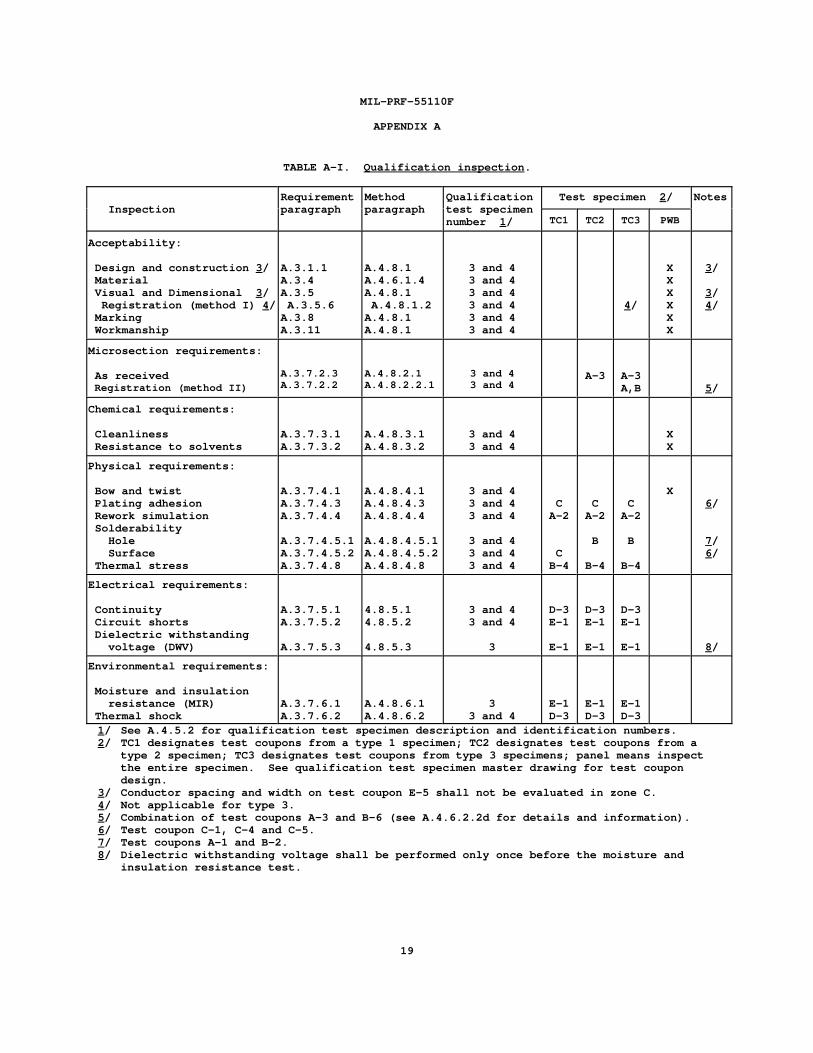
TABLE A-I. Qualification inspection .
InspectionRequirementparagraph
Methodparagraph
Qualificationtest specimennumber 1 /
Test specimen 2 / Notes
TC1 TC2 TC3 PWB
Acceptability:
Design and construction 3 / Material Visual and Dimensional 3 / Registration (method I) 4 / Marking Workmanship
A.3.1.1A.3.4A.3.5 A.3.5.6A.3.8A.3.11
A.4.8.1A.4.6.1.4A.4.8.1 A.4.8.1.2A.4.8.1A.4.8.1
3 and 43 and 43 and 43 and 43 and 43 and 4
4/
XXXXXX
3/
3/4/
Microsection requirements:
As received Registration (method II)
A.3.7.2.3A.3.7.2.2
A.4.8.2.1A.4.8.2.2.1
3 and 43 and 4
A-3 A-3A,B 5 /
Chemical requirements:
Cleanliness Resistance to solvents
A.3.7.3.1A.3.7.3.2
A.4.8.3.1A.4.8.3.2
3 and 43 and 4
XX
Physical requirements:
Bow and twist Plating adhesion Rework simulation Solderability Hole Surface Thermal stress
A.3.7.4.1A.3.7.4.3A.3.7.4.4
A.3.7.4.5.1A.3.7.4.5.2A.3.7.4.8
A.4.8.4.1A.4.8.4.3A.4.8.4.4
A.4.8.4.5.1A.4.8.4.5.2A.4.8.4.8
3 and 43 and 43 and 4
3 and 43 and 43 and 4
CA-2
CB-4
CA-2
B
B-4
CA-2
B
B-4
X6/
7/6/
Electrical requirements:
Continuity Circuit shorts Dielectric withstanding voltage (DWV)
A.3.7.5.1A.3.7.5.2
A.3.7.5.3
4.8.5.14.8.5.2
4.8.5.3
3 and 43 and 4
3
D-3E-1
E-1
D-3E-1
E-1
D-3E-1
E-1 8 /
Environmental requirements:
Moisture and insulation resistance (MIR) Thermal shock
A.3.7.6.1A.3.7.6.2
A.4.8.6.1A.4.8.6.2
33 and 4
E-1D-3
E-1D-3
E-1D-3
1/ See A.4.5.2 for qualification test specimen description and identification numbers.2/ TC1 designates test coupons from a type 1 specimen; TC2 designates test coupons from a
type 2 specimen; TC3 designates test coupons from type 3 specimens; panel means inspectthe entire specimen. See qualification test specimen master drawing for test coupondesign.
3/ Conductor spacing and width on test coupon E-5 shall not be evaluated in zone C.4/ Not applicable for type 3.5/ Combination of test coupons A-3 and B-6 (see A.4.6.2.2d for details and information).6/ Test coupon C-1, C-4 and C-5.7/ Test coupons A-1 and B-2.8/ Dielectric withstanding voltage shall be performed only once before the moisture and
insulation resistance test.
MIL-PRF-55110F
APPENDIX A
20
A.4.5.3.1 Manufacturer test routine . The manufacturer shall perform the inspectionsspecified in tables A-II and A-III (in-process and group A inspection).
A.4.5.3.2 Acceptable qualification laboratory test routine . The qualification laboratoryacceptable to the Government shall subject the qualification test specimens to theinspections specified in table A-I. The order of the inspections and tests is optional;however, the cleanliness test shall be performed first.
A.4.5.3.3 Contract services . Manufacturers wanting to use an external subcontractedservice for production of printed wiring board shall first qualify using their own internalequipment/processes within its facility. Once qualified internally, a manufacturer mayqualify using the subcontracted service. This additional subcontracted qualification willnot be listed separately on the QPL. The subcontract service shall not be extended toanother external subcontracted service or manufacturer.
NOTE: For the purposes of this appendix, the internal equipment/process condition appliesonly to those processes used to manufacture the qualification test specimen. When applyingfor qualification of sub-contracted services, the process and the company performing thesub-contracted service shall be identified. If the manufacturer does not have any internalcapability to perform a certain production step (either used during qualification or onlyused during production) this shall be identified on the application for authorization totest. If the sub-contracted service is changed, the manufacturer shall requalify.
A.4.5.3.4 Qualification rejection . Qualification approval will not be granted if any ofthe qualification test specimens tested in accordance with table A-I fail to meet thespecified requirements.
A.4.5.4 Extent of qualification .
A.4.5.4.1 Printed wiring board type . Qualification of a particular printed wiring boardtype shall be extended to cover all conductive patterns of that same printed wiring boardtype produced. Qualification of type 3 printed wiring boards shall be extended to covertype 1 and type 2 printed wiring boards. Qualification of type 2 printed wiring boardsshall be extended to cover type 1 printed wiring boards.
A.4.5.4.2 Base material types . Extension of qualification using base laminate materialsin accordance with MIL-S-13949 shall be as follows:
a. Qualification with type GF base materials shall be extended to cover types GB and GHbase materials.
b. Qualification with type GR base materials shall be extended to cover type GP basematerials.
c. Qualification with type GY base materials shall be extended to cover types GT and GXbase materials.
d. Qualification with type GX base materials shall be extended to cover type GT basematerial.
e. Qualification with type SC base materials shall be extended to cover type GC basematerial.
f. Qualification with types AF, BF, BI, GB, GC, GH, GI, GM, GP, GT, or QI shall cover thatbase material only.
A.4.5.4.3 Mass lamination (see A.6.4.4.1) . Qualification of a contract lamination (tenconductor layers) shall be extended to cover a contract lamination of three or moreconductor layers. The test specimens for ten layer contract lamination shall meet therequirements specified in master drawing IPC-100043.
MIL-PRF-55110F
APPENDIX A
21
A.4.5.4.4 Processes .
A.4.5.4.4.1 Etchback . Qualification using etchback shall be extended to covernon-etchback.
A.4.5.4.4.2 Process changes . Any changes to a manufacturers qualified base material type,equipment, or processes must be reviewed by the qualifying activity for determination ifpartial or full requalification is necessary.
A.4.5.5 Retention of qualification . To retain qualification, the manufacturer shallcertify to the qualifying activity that they still have the capability of manufacturing andverifying printed wiring boards which meet the performance requirements of this document. Refer to the qualifying activity for any additional guidelines necessary to retainqualification to this document. The manufacturer shall immediately notify the qualifyingactivity at any time that the inspection data indicates failure of the qualified product tomeet the performance requirements, of this document.
A.4.5.5.1 Requalification (see A.6.3.2) . Qualifications expire 36 months from the date ofinitial qualification. In order to maintain a QPL listing, manufacturers shall completerequalification before the end of its current 36 month qualification.
A.4.5.5.2 Product assurance information . The manufacturer shall make available toqualifying activity an approved quality manual or procedures that as a minimum addresses thefollowing information:
a. In-process and group A verification procedures.
b. Test coupon quantity, design, placement and usage procedures.
c. The definition of complexity used to select samples for group B verification testing.
A.4.6 Inspection of product for delivery . Inspection of product for delivery shallconsist of in-process and group A inspection. Except as specified in A.4.7.1.4, delivery ofprinted wiring boards which have passed in-process and group A inspection shall not bedelayed pending the results of the periodic inspection. Anomalies or defects noted onsample printed wiring boards or test coupons (or both) defined herein shall be recorded andthe proper corrective action shall be initiated. Manufacturers that are qualified to usesubcontract services are still responsible for in-process and groups A inspections and shallbe subject to loss of qualification if the results of in-process and group A inspectionsindicate failure to meet the applicable requirements.
A.4.6.1 In-process inspection . Each inspection lot of printed wiring boards or panels, asapplicable shall be inspected in accordance with table A-II, as applicable. When permanentsolder resist is specified (see A.3.1.1), the in-process inspections specified in subgroups1, 2 and 3 of table A-II shall be performed prior to solder resist application. Prior tolamination of type 3 printed wiring boards, the in-process inspections specified in subgroup2 of table A-II shall be performed.
A.4.6.1.1 Inspection lot .
A.4.6.1.1.1 Subgroup 1 . An inspection lot shall correspond to each change of shift orwork force, whichever occurs first. Production lots may be grouped based on same materials,same type or types of interfacial connections and terminations, and same processingrequirements.
A.4.6.1.1.2 Subgroups 2 and 3 . An inspection lot shall consist of the number of printedwiring boards fabricated from the same materials, using the same processing procedures,produced under the same conditions within a maximum period of 1 month and offered forinspection at one time.
MIL-PRF-55110F
APPENDIX A
22
TABLE A-II. In-process inspection .
Inspection Requirementparagraph
Methodparagraph
Sample size 1 /
Subgroup 1
MaterialCleanliness 2 /
A.3.4A.3.7.3.1.1
A.4.8.1A.4.8.3.1
See A.4.6.1.4Plan *L
Subgroup 2
Conductor spacing 2 / 3 / Conductor width 2 / 3 /Conductive pattern imperfections
A.3.5.2.2A.3.5.2.3A.3.5.2.4
A.4.8.1A.4.8.1A.4.8.1
Plan BHPlan BHPlan BH
Subgroup 3
Plating adhesion 2 / 4 / A.3.7.4.3 A.4.8.4.3 Plan BH
1/ See appendix C, table C-I for C = 0 sampling plans and C.4.5 for examples.2/ Performed prior to solder resist application.3/ Performed prior to lamination on each production lot.4/ A Non-reflowed test coupon prior to reflow may be required (see A.6.2).
A.4.6.1.2 Sample size . The number of printed wiring boards or panels to be selected fromeach inspection lot shall be in accordance with table A-II.
A.4.6.1.3 Rejected lots . If an inspection lot is rejected as a result of a failure topass the subgroup 1 test specified, the manufacturer shall withdraw the lot, take correctiveaction in connection with the cleaning materials and procedures, reclean the lot andresubmit the lot for inspection prior to application of permanent solder resist coating. Printed wiring boards are not acceptable if the permanent solder resist coating has beenapplied to a contaminated surface. If an inspection lot is rejected for subgroup 2 or 3tests, the manufacturer may screen (100 percent inspection) out the defective units (printedwiring boards or panels). Defective printed wiring boards shall not be shipped.
A.4.6.1.4 Materials inspection . Materials inspection shall consist of certificationsupported by verifying data that the materials used in fabricating the printed wiring boardsare in accordance with the applicable referenced specifications or requirements specified(see A.3.1.1), prior to such fabrication. Unless otherwise specified (see A.3.1.1),verifying data need not be submitted to the qualifying activity or acquiring activity, butmust be made available upon request.
A.4.6.2 Group A inspection . Group A inspection shall consist of the inspections specifiedin table A-III. The qualified manufacturer shall be responsible for completion of all groupA inspections and shall be subject to loss of qualification for failure not to complete orto have completed all group A test and inspections (see appendix D for group A VCI options).
A.4.6.2.1 Inspection lot . A group A inspection lot shall consist of the number of printedwiring boards fabricated from the same materials, using the same processing procedures,produced under the same conditions within a maximum period of 1 month and offered forinspection at one time.
A.4.6.2.2 Sampling procedures . Statistical sampling and inspection shall be in accordancewith appendix C. For 100 percent inspection, all rejected units (printed wiring boards orpanels of printed wiring boards) shall not be supplied as compliant. The following detailson panel/test coupon sampling shall apply:
a. Solderability : For SERA, samples shall be selected in accordance with appendix E; ForJ-STD-003, samples shall be selected in accordance with appendix C, table C-I, plan L.
MIL-PRF-55110F
APPENDIX A
23
b. As received:
1) Types 1 and 2 : The number of test coupons to be microsectioned shall be based ona statistical sample of panels in the lot in accordance with appendix C, plan L.
2) Type 3 : A minimum of one test coupon per panel shall be microsectioned.
c. Thermal stress:
1) Types 1 and 2 : The number of test coupons to be microsectioned shall be based ona statistical sample of panels in the lot in accordance with appendix C, plan L.
2) Type 3 : A minimum of two test coupons (A's, B's or combination of both) per panelshall be microsectioned. One of the test coupon shall be microsectioned in thepanel's length direction and the other shall be microsectioned along the panel'swidth direction.
d. Registration (method II, type 3 only) : When method II is to be used, registrationshall be evaluated using any combination of two microsectioned test specimens takenfrom diagonal corners of the panel. Both test coupons shall have been microsectionedin the vertical plane with one test coupon representing the panel's length (X)direction and the other representing the panel's width (Y) direction. Test couponsfrom the AS RECEIVED (see A.3.7.2.1), THERMAL STRESS (see A.3.7.4.8.2) or whenavailable, HOLE SOLDERABILITY (see A.3.7.4.5) verifications may be used.
A.4.6.2.3 Rejected lots . If an inspection lot is rejected, the manufacturer may rework itto correct the defects and resubmit the lot for reinspection, or screen out the defectiveunits (if possible). Resubmitted lots shall be inspected using tightened inspection (plan Tor Q of table VII, as applicable). Such lots (reworked or screened) shall be clearlyidentified as reinspected lots. Products which have failed any group A inspection and havenot been reworked and have not passed reinspection (as specified in this appendix) may notbe delivered as compliant printed wiring boards.
A.4.6.2.4 Disposition of sample units and test coupons . Sample printed wiring boardswhich have passed all of group A inspection may be delivered if the inspection lot isaccepted. Test coupons which have been subjected to group A shall be retained as specifiedin A.3.9.
A.4.7 Periodic inspection . Periodic inspection shall consist of group B inspection. Except where these inspections show noncompliance (see A.4.7.1.4) with the applicablerequirements of this document and the master drawing, delivery of printed wiring boardswhich have passed group A shall not be delayed pending the results of these periodicinspections. Periodic inspections shall be performed at a laboratory acceptable to theGovernment (see A.6.6).
A.4.7.1 Group B inspection . Group B inspection shall consist of the inspections specifiedin table A-IV (see appendix D for group B VCI options).
A.4.7.1.1 Inspection lot . The sample units (test coupons) shall be randomly selected fromthe most complex (see A.6.4.2) inspection lot that has passed all in-process and group Ainspections during that production month. The most complex printed wiring boards shall beas determined by the manufacturer using its definition of complex (see A.6.4.2), subject toapproval by the qualifying activity.
A.4.7.1.2 Sampling procedures . The selection of sample units and testing shall be on amonthly basis. Samples for each extent of qualification base material type family (seeA.4.1.2) produced during that reporting period shall be subjected to group B inspection. Because of the performance nature of this document, the design details of the test couponswill need to be supplied with the sample units (see A.6.8).
MIL-PRF-55110F
APPENDIX A
24
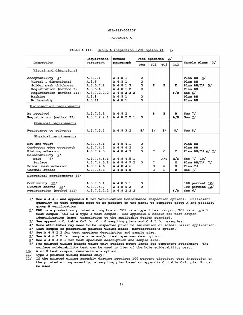
TABLE A-III. Group A inspection (VCI option 4) . 1 /
InspectionRequirementparagraph
Methodparagraph
Test specimen 2 /Sample plans 3 /
PWB TC1 TC2 TC3
Visual and dimensional
Acceptability 4 / Visual & dimensional Solder mask thickness Registration (method I) Registration (method III) Marking Workmanship
A.3.7.1A.3.5A.3.5.7.2A.3.5.6A.3.7.2.2.2A.3.8A.3.11
A.4.8.1A.4.8.1A.4.8.1.3A.4.8.1.2A.4.8.2.2.2A.4.8.1A.4.8.1
XXXX
XX
E E E
F/R
Plan BH 4 /Plan BHPlan BH/TJ 5 /Plan BHSee 6 /Plan BHPlan BH
Microsection requirements
As receivedRegistration (method II)
A.3.7.2.1A.3.7.2.2.1
A.4.8.2A.4.8.2.2.1 X
B B BA/B
See 7 /See 7 /
Chemical requirements
Resistance to solvents A.3.7.3.2 A.4.8.3.2 8 / 8 / 8 / 8 / See 8 /
Physical requirements
Bow and twistConductor edge outgrowthPlating adhesionSolderability 9 / Hole 9 / SurfaceSolder mask adhesionThermal stress
A.3.7.4.1A.3.7.4.2A.3.7.4.3
A.3.7.4.5.1A.3.7.4.5.2A.3.7.4.6A.3.7.4.8
A.4.8.4.1A.4.8.4.2A.4.8.4.3
A.4.8.4.5.1A.4.8.4.5.2A.4.8.4.6A.4.8.4.8
XXX
X
C
CGB
C
A/S
GB
C
A/SMGB
Plan BHPlan BHPlan BH/TJ 4 / 7 /
See 7 / 10 /Plan BH/TJ 7 /Plan TJSee 7 /
Electrical requirements 11 /
Continuity 12 /Circuit shorts 12 /Registration (method III)
A.3.7.5.1A.3.7.5.2A.3.7.2.2.2
A.4.8.5.1A.4.8.5.2A.4.8.2.2.2
XX
F/R
100 percent 12 /100 percent 12 /See 6 /
1/ See A.4.4.1 and appendix D for Verification Conformance Inspection options. Sufficientquantity of test coupons need to be present on the panel to complete group A and possiblygroup B verification.
2/ PWB is a production printed wiring board; TC1 is a type 1 test coupon; TC2 is a type 2test coupon; TC3 is a type 3 test coupon. See appendix D herein for test couponidentification (name) translation to the applicable design standard.
3/ See appendix C, table C-I for C = 0 sampling plans and C.4.5 for examples.4/ Some attributes may need to be inspected prior to lamination or solder resist application.5/ Test coupon or production printed wiring board, manufacturer's option.6/ See A.4.8.2.2 for test specimen description and sample size.7/ See A.4.6.2.2 for sample size and/or test specimen description.8/ See A.4.8.3.2.1 for test specimen description and sample size.9/ For printed wiring boards using only surface mount lands for component attachment, the
surface solderability test can be used in lieu of the hole solderability test.10/ A or S test coupon, manufacturers option.11/ Type 3 printed wiring boards only.12/ If the printed wiring assembly drawing requires 100 percent circuitry test inspection on
the printed wiring assembly, a sampling plan based on appendix C, table C-I, plan F, canbe used.
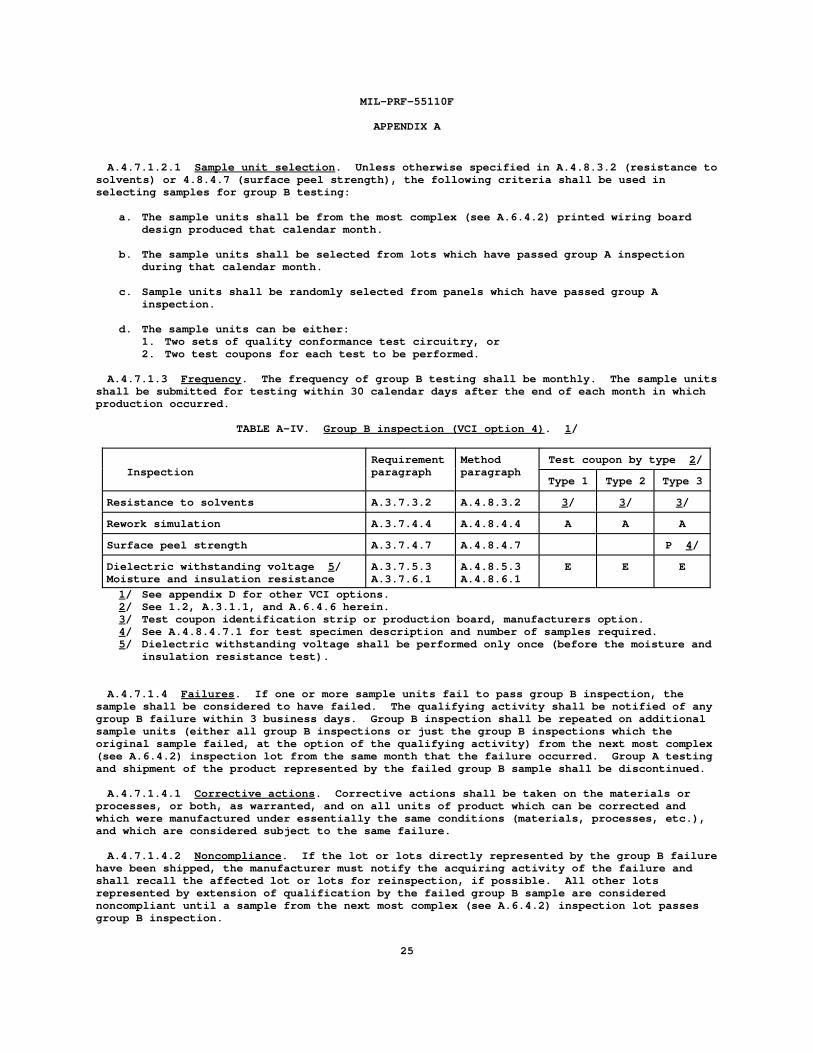
MIL-PRF-55110F
APPENDIX A
25
A.4.7.1.2.1 Sample unit selection . Unless otherwise specified in A.4.8.3.2 (resistance tosolvents) or 4.8.4.7 (surface peel strength), the following criteria shall be used inselecting samples for group B testing:
a. The sample units shall be from the most complex (see A.6.4.2) printed wiring boarddesign produced that calendar month.
b. The sample units shall be selected from lots which have passed group A inspectionduring that calendar month.
c. Sample units shall be randomly selected from panels which have passed group Ainspection.
d. The sample units can be either:1. Two sets of quality conformance test circuitry, or2. Two test coupons for each test to be performed.
A.4.7.1.3 Frequency . The frequency of group B testing shall be monthly. The sample unitsshall be submitted for testing within 30 calendar days after the end of each month in whichproduction occurred.
TABLE A-IV. Group B inspection (VCI option 4) . 1 /
InspectionRequirementparagraph
Methodparagraph
Test coupon by type 2 /
Type 1 Type 2 Type 3
Resistance to solvents A.3.7.3.2 A.4.8.3.2 3 / 3 / 3 /
Rework simulation A.3.7.4.4 A.4.8.4.4 A A A
Surface peel strength A.3.7.4.7 A.4.8.4.7 P 4 /
Dielectric withstanding voltage 5 /Moisture and insulation resistance
A.3.7.5.3A.3.7.6.1
A.4.8.5.3A.4.8.6.1
E E E
1/ See appendix D for other VCI options.2/ See 1.2, A.3.1.1, and A.6.4.6 herein.3/ Test coupon identification strip or production board, manufacturers option.4/ See A.4.8.4.7.1 for test specimen description and number of samples required.5/ Dielectric withstanding voltage shall be performed only once (before the moisture and
insulation resistance test).
A.4.7.1.4 Failures . If one or more sample units fail to pass group B inspection, thesample shall be considered to have failed. The qualifying activity shall be notified of anygroup B failure within 3 business days. Group B inspection shall be repeated on additionalsample units (either all group B inspections or just the group B inspections which theoriginal sample failed, at the option of the qualifying activity) from the next most complex(see A.6.4.2) inspection lot from the same month that the failure occurred. Group A testingand shipment of the product represented by the failed group B sample shall be discontinued.
A.4.7.1.4.1 Corrective actions . Corrective actions shall be taken on the materials orprocesses, or both, as warranted, and on all units of product which can be corrected andwhich were manufactured under essentially the same conditions (materials, processes, etc.),and which are considered subject to the same failure.
A.4.7.1.4.2 Noncompliance . If the lot or lots directly represented by the group B failurehave been shipped, the manufacturer must notify the acquiring activity of the failure andshall recall the affected lot or lots for reinspection, if possible. All other lotsrepresented by extension of qualification by the failed group B sample are considerednoncompliant until a sample from the next most complex (see A.6.4.2) inspection lot passesgroup B inspection.
MIL-PRF-55110F
APPENDIX A
26
A.4.7.1.4.3 Reinstitution of Group A inspection . After successful completion of group Breinspection, group A inspection of product represented by the group B failure may bereinstituted.
A.4.7.1.5 Disposition of sample units . Test coupons which have been subjected to group Bshall be retained as specified in A.3.9.
A.4.8 Methods of inspection . The following identified tests and test methods assureprinted wiring board integrity with typical operating conditions. Alternate commercial orindustry standard test methods may be allowed, however if an alternate method is to be used,the qualifying activity must be notified prior to the performance of the test. Thefollowing verification test methods described herein are proven methods and shall be thereferee method in case of dispute.
A.4.8.1 Acceptability inspection . The visual and dimensional features of the printedwiring board test specimen shall be inspected using either an optical apparatus or aid whichprovides a minimum magnification of 1.75x (3 diopters) or by using automated inspectiontechniques. Referee inspection of the specimen features shall be accomplished at amagnification of 10X.
A.4.8.1.1 Annular ring, external (see A.3.5.2.1) . The measurement of the annular ring onexternal layers is from the inside surface (within the hole) of the plated hole orunsupported hole to the outer edge of the annular ring on the surface of the printed wiringboard (see IPC-TM-650, method 2.2.1 for illustration).
A.4.8.1.2 Registration (method I)(Types 1 and 2)(see A.3.5.6) . Layer-to-layerregistration of type 1 and type 2 printed wiring boards shall be satisfied if the outerlayers meet the external annular ring (see 3.1 and A.3.5.2.1) and hole pattern accuracy (seeA.3.1.1 and A.3.5.4) requirements.
A.4.8.1.3 Solder resist thickness (see A.3.5.7.4) . Solder resist thickness shall beinspected by any micrometer or by microsection in accordance with A.4.8.2.
A.4.8.2 Microsection inspection . Microsection inspections (to evaluate characteristicssuch as plated-through holes, plating thickness, or foil thickness) shall be accomplished byusing methods in accordance with either IPC-TM-650, method 2.1.1 or 2.1.1.2. The followingdetails shall apply:
a. Number of holes per specimen . A minimum of one microsection containing at least threeplated-through holes shall be made for each test specimen required. Each side of theplated hole shall be viewed independently.
b. Accuracy . Plated-through holes shall be microsectioned in the vertical plane at thecenter of the hole ±10 percent.
c. Magnifications . The specimens shall be inspected for foil and plating integrity at amagnification of 100X ±5 percent. Referee inspections shall be accomplished at amagnification of 200X ±5 percent.
d. Evaluations . Evaluations for items such as base material thickness, metal foilthickness, plating thickness, lay-up orientation, resin smear, and plating voids shallbe accomplished at magnifications specified above. If resin smear is detected orsuspected on a vertical microsection, a referee microsection shall be prepared andevaluated in the annular (horizontal) direction.
e. Measurements . Measurements shall be averaged from at least three determinations foreach side of the plated-through hole. Isolated thick or thin sections shall not beused for averaging, however, isolated areas of reduced copper thickness shall bemeasured and evaluated to the copper plating void rejection criteria specified herein.
MIL-PRF-55110F
APPENDIX A
27
A.4.8.2.1 Plated-through hole inspection (see A.3.6) . When inspected in accordance with4.8.2, the following details shall apply:
a. Annular ring (internal) (see A.3.6.1) . This measurement shall apply to all internallands for all three holes.
b. Dielectric layer thickness (see A.3.6.3) . The dielectric layer thickness shall beinspected between all conductor layers present in the test specimen.
c. Plating and coating thickness (see A.3.6.8) . Isolated thick or thin sections shall notbe used for averaging. However, isolated areas of reduced copper thickness shall bemeasured for compliance with the requirements of A.3.6.8.
d. Copper plating voids (see A.3.6.9.1) . Any plated-through hole in the microsectionfailing the plating void criteria A.3.6.9.1 subparagraphs a, b or c, shall be cause forthe entire panel of printed wiring boards associated with the microsection to berejected. The following details apply if a single plating void is found:
(1) Type 2: If the plating void does not exceed the conditions of A.3.6.9.1, theentire lot (100 percent panel inspection) shall be microsectioned and inspectedfor voids. If a plating void is present on any panel, a referee microsectionshall be performed using an A or B test coupon from the opposite corner of thatpanel. If the referee has no plating voids, that panel is acceptable, however, ifa plating void is present in that microsection, that panel of printed wiringboards shall be rejected.
(2) Type 3: If the plating void does not exceed the conditions of A.3.6.9.1, a refereemicrosection shall be performed using an A or B test coupon from the oppositecorner of the panel. If the referee has no plating voids, the panel isacceptable, however, if a plating void is present in that microsection, that panelof printed wiring boards shall be rejected.
e. Thermal planes (see A.3.6.3.1) . The lateral dielectric spacing between the heatsinking planes and adjacent conducting surfaces (nonfunctional lands) or plated-throughholes shall be measured at the closest point between these surfaces or theplated-through hole.
A.4.8.2.2 Registration (internal) . Internal layer-to-layer registration shall bedetermined by either evaluating microsectioned test coupons (method II, see A.4.8.2.2.1) orthe use of registration test coupons and techniques (method III, see A.4.8.2.2.2).
A.4.8.2.2.1 Method II (by microsectioned sample units) . The two microsectioned testcoupons shall be evaluated by computing the difference in centerline location of the twolands found to be most eccentric to one another within each cross-section (see IPC-TM-650,method 2.2.11 for illustration).
A.4.8.2.2.2 Method III (by registration test coupons) . Registration test coupons andtechniques, when provided by the printed wiring board fabricator, shall be evaluated inaccordance with methods approved by the qualifying activity and when applicable, theacquiring activity. Unapproved methods of measurement using registration test coupons shallbe backed up by method II of A.4.8.2.2.1 using the appropriate test coupons (see tableA-III) from the same panel. Two non-destructive methods for determining registration areavailable using the following test coupon designs:
a. Test coupon F (etch factor not needed).
b. Test coupon R (etch factor of each layer needed).
If other registration test coupon designs and requirements are provided as an element ofthe design documentation set, registration can be evaluated in accordance with the criteriaspecified on the applicable master drawing.
MIL-PRF-55110F
APPENDIX A
28
A.4.8.3 Chemical inspection .
A.4.8.3.1 Cleanliness (by resistivity of solvent extract) (see A.3.7.3.1 and 6.5) . Theprinted wiring board shall be inspected for cleanliness in accordance with IPC-TM-650,method 2.3.25.
A.4.8.3.2 Resistance to solvents (marking ink or paint) (see A.3.7.3.2) . Marking ink orpaint resistance to solvents shall be inspected in accordance with IPC-TM-650, method 2.3.4. The following details apply:
a. The marked portion of the test specimen shall be brushed.
b. After the test, the test specimen shall be visually inspected in accordance withA.4.8.1 for legibility of marking.
A.4.8.3.2.1 Sampling procedures and test specimens . The resistance to solvents test shallbe performed either during group A (every lot) or during group B (monthly). The testspecimens can be either production printed wiring boards or quality conformance testcircuitry strip identification areas (see appendix D) containing ink or paint marking. Foreither group A or group B, the minimum number of samples shall be at least one sample foreach solution specified by the applicable test method (i.e., one sample for each solutionrequired).
A.4.8.4 Physical inspections .
A.4.8.4.1 Bow and twist (see A.3.7.4.1) . The printed wiring board shall be inspected forbow and twist in accordance with IPC-TM-650, method 2.4.22.
A.4.8.4.2 Conductor edge outgrowth (see A.3.7.4.2) . The extent of outgrowth, onconductors covered with metals other than fused tin-lead or solder coating, shall bedetermined by measuring the conductor width before and after mechanically removing theoverhang metal. If a referee test is required, cross-sectioning of the conductor shall beperformed. The procedure for removing overhang metal, for this test, shall be as follows:
a. Wet the printed wiring board specimen in tap water at approximately room temperature.
b. While wet, brush the printed wiring board specimen with a brass wire brush to removethe overhang metal. Brush in the direction of the functional line, using moderatepressure.
A.4.8.4.3 Plating adhesion (see A.3.7.4.3) . The printed wiring board shall be inspectedin accordance with IPC-TM-650, method 2.4.1, with the following details and exceptions. When edge board contacts are part of the pattern, at least one pull must be on the contacts. Fresh tape shall be used for each pull. If overhang metal breaks off (slivers) and adheresto the tape, it is evidence of outgrowth (see A.3.7.4.2), but not a plating adhesionfailure.
A.4.8.4.4 Rework simulation .
A.4.8.4.4.1 Type 1 (unsupported hole) (see A.3.7.4.4.1) . The printed wiring board testspecimen shall be inspected in accordance with IPC-TM-650, method 2.4.21 with the followingdetails and exceptions: Three holes per test coupon shall be tested. Insert wires in holesin selected lands and solder to lands by machine or hand, as applicable. The insert wirelead shall have a diameter so that the diameter of the hole will be at a maximum of .020inch (0.51 mm) greater than the diameter of the inserted wire lead. The wires shall not beclinched. It shall be considered a failure when a land around an unsupported hole isloosened.
MIL-PRF-55110F
APPENDIX A
29
A.4.8.4.4.2 Types 2 and 3 (see A.3.7.4.4.2) . Rework simulation of plated-through holesshall be tested in accordance with IPC-TM-650, method 2.4.36, except that the reworksimulation shall be performed after stabilizing the test coupons at temperatures of 15 (C to35(C and relative humidity of 40 to 85 percent for a period of 24 hours.
A.4.8.4.4.3 Surface mount land . The surface mount lands on the printed wiring board testspecimen shall be inspected in accordance with IPC-TM-650, method 2.4.21.1.
A.4.8.4.5 Solderability (see A.3.7.4.5) .
A.4.8.4.5.1 Hole (plated-through hole)(Types 2 and 3)(see A.3.7.4.5.1) . The printedwiring board test specimens shall be inspected in accordance with J-STD-003 class 3 orappendix E.
A.4.8.4.5.2 Surface (Type 1 or surface mount land)(see A.3.7.4.5.2) . The printed wiringboard test specimens shall be inspected in accordance with J-STD-003 class 3 or appendix E.
A.4.8.4.6 Solder resist adhesion (see A.3.7.4.6) . The permanency and adhesion of curedsolder resist shall be determined in accordance with IPC-TM-650, method 2.4.28.1.
A.4.8.4.7 Surface peel strength (type 3 using foil lamination)(see A.3.7.4.7) . The peelstrength shall be inspected in accordance with IPC-TM-650, method 2.4.8, except that theafter thermal stress condition and after exposure to processing chemicals tests shall not beperformed. Plated tin-lead, solder coating, or other plated metallic resist shall bechemically removed prior to test or shall be prevented from being deposited duringmanufacturing. The test specimen shall not be coated with any organic coating for test. All peel strength readings obtained shall meet the minimum requirement.
A.4.8.4.7.1 Test specimens . The specimen shall consist of conductors that provide aminimum test length of 2 inches (50.8 mm) and a conductor width of .125 inch (3.3 mm). NOTE: This test coupon is described in the design standard for VCI option 4 (test coupon"P") or IPC-TM-650, section 5.8.3. At least one test coupon per foil laminated side shallbe placed on the panel where space is available. Eight peel strength specimens shall beselected from two different production lots; four from each lot or 100 percent if the numberof coupons available is less than four for a production lot. If only one foil laminated lotis submitted/passes group A inspection in a calendar month, then only the test coupon(s)from that lot shall be submitted.
A.4.8.4.8 Thermal stress (see A.3.7.4.8) . The printed wiring board test specimen shall beinspected for thermal stress in accordance with IPC-TM-650, method 2.6.8.
A.4.8.5 Electrical inspection .
A.4.8.5.1 Continuity (see A.3.7.5.1) . A current shall be passed through each conductor orgroup of interconnected conductors by applying electrodes on the terminals at each end ofthe conductor or group of conductors. The current passed through the conductors shall notexceed those specified in the applicable design standard (see A.3.1.1 and appendix D) forthe smallest conductor in the circuit.
A.4.8.5.2 Circuit shorts (see A.3.7.5.2) . A test voltage shall be applied between allcommon portions of each conductive pattern and all adjacent common portions of eachconductive pattern. The voltage shall be applied between conductive patterns of each layerand the electrically isolated pattern of each adjacent layer. For manual testing thevoltage shall be 200 volts minimum and shall be applied for a minimum of 5 seconds. Whenautomated test equipment is used, the minimum applied test voltage shall be as specified onthe applicable master drawing. If a test voltage of the printed wiring board is notspecified on the applicable master drawing, the test voltage shall be the maximum ratedvoltage of the printed wiring board or 40 volts minimum, whichever is less.
MIL-PRF-55110F
APPENDIX A
30
A.4.8.5.3 Dielectric withstanding voltage (see A.3.7.5.3) . The printed wiring board testspecimen shall be tested in accordance with IPC-TM-650, method 2.5.7. The following detailsand exceptions apply:
a. Magnitude of test voltage: 1,000 V dc +25 V dc, -0 V dc.
b. Duration of application of test voltage: 30 seconds +3, -0 seconds.
c. Points of application: The dielectric withstanding voltage shall be applied betweenall common portions of each conductive pattern and all adjacent common portions ofeach conductive pattern. The voltage shall be applied between conductive patterns ofeach layer and the electrically isolated pattern of each adjacent layer.
A.4.8.6 Environmental inspection .
A.4.8.6.1 Moisture and insulation resistance (see A.3.7.6.1) . The printed wiring boardtest specimen shall be tested in accordance with IPC-TM-650, method 2.6.3, class 3.
A.4.8.6.1.1 Non-component (flush conductor) printed wiring boards (see A.3.7.6.1.1) . Thespecimens shall be inspected in accordance with A.4.8.6.1, except the insulation resistancemeasurement shall be taken within 1 minute after the removal of the specimen from thehumidity chamber after 100 V dc, ±15 percent has been applied between all conductors for aminimum of 60 seconds.
A.4.8.6.2 Thermal shock (see A.3.7.6.2) . The printed wiring board test specimen shall betested in accordance with IPC-TM-650, method 2.6.7.2, with the following exceptions:
a. The printed wiring board test specimens shall be subjected to 100 temperature cyclesin accordance with the table A-V following:
b. Transfer time between chambers shall be less than 2 minutes. The thermal capacity ofthe test chambers used shall be such that the ambient temperature shall reach thespecified temperature within 2 minutes after the specimen has been transferred to theappropriate chamber.
c. The following measurements shall be made:
1. Before test: Resistance.
2. During the test: Resistance during the first and last high temperature cycle:
3. After the test: Resistance.
TABLE A-V. Thermal shock, temperatures and times .
Low temperature+0(C/-5 (C
Time (minutes)+2/-0
High temperature+5(C/-0 (C
Time (minutes)+2/-0
Base material type(seeappendix D)
-65 15 85 15 GR, GP, GT, GY, GX
-65 15 125 15 AF, BF, BI, GC, GF,GH, SC
-65 15 150 15 GB, GM,
-65 15 175 15 AI, GI, QI
MIL-PRF-55110F
APPENDIX A
31
A.5 PACKAGING
A.5.1 Packaging requirements . The requirements for packaging shall be in accordance withthe purchase order or contract (see A.6.2).
A.6 NOTES
(This section contains information of a general or explanatory nature that may be helpful,but is not mandatory.)
A.6.1 Intended use . This appendix is intended to be used by manufacturer's not certifiedto the QML printed board specification, MIL-PRF-31032. This appendix is not a duplicate orlook-alike of any MIL-PRF-31032 associated specification, most of the historic performanceand verification requirements are still contained in this appendix. However, many of the"enhanced" acceptance criteria or methods developed for MIL-PRF-31032 associatedspecifications have been added as the baseline or are available as an option.
A.6.2 Acquisition requirements .
A.6.2.1 Acquisition documents . Acquisition documents should specify the following:
a. Title, number, revision letter (with any amendment number when applicable), and dateof this specification.
b. Issue of DODISS to be cited in the solicitation, and if required, the specific issueof individual documents referenced (see 2.2, A.2.1 and A.2.2).
c. Appropriate type (see 1.2.1) and base material designation (see 1.2.2).
d. Title, number, revision letter (with any engineering change proposal or notice ofrevision number when applicable), and date of the applicable master drawing (seeA.3.1.1).
e. Title, number, revision letter (with any notice number when applicable), and date ofthe applicable design standard (see A.3.3).
f. Part identification (if applicable), and marking instructions including size, locationand application method (see A.3.1.1 and A.3.8).
g. Whether microsectioned test specimens, samples or photographs are required to bedelivered with the order.
h. Levels of preservation and packing required (see A.5.1).
A.6.2.2 Additional acquisition requirements . Acquisition documents should also specifythe following data, if applicable:
a. Verification Conformance Inspection option (if other than option 4)(see appendix D).
b. Design related if different than the applicable design standard (see appendix D).
1. Minimum annular ring (external or internal)(see A.3.1.1), if different than theapplicable design standard.
2. Minimum conductor width (see A.3.1.1), if different than the applicable designstandard.
3. Minimum conductor spacing (see A.3.1.1), if different than the applicable designstandard.
MIL-PRF-55110F
APPENDIX A
32
4. Minimum dielectric thickness (see A.3.1.1), if different than the applicable designstandard.
5. Minimum edge spacing requirement (see A.3.1.1), if different than the applicabledesign standard.
6. Copper plating thickness (see A.3.1.1), if different than the applicable designstandard.
7. Conductor finish plating (see A.3.1.1), if other than solder coating or tin-lead.
c. Conductor edge overhang, if applicable (see A.3.7.4.2).
d. Insulation resistance requirements (see A.3.7.5.2).
e. Foil lamination peel strength, if applicable (see A.3.7.4.7).
f. Nondelivery of sample units which have not been subjected to the continuity test andhave passed all other tests to groups A and B inspection.
g. Cleanliness (organic)(see A.3.7.3.1.2 and A.6.5.3).
h. If special or other identification marking is required (see A.3.8).
A.6.3 Qualification notes . Although the qualification test specimen master drawingsspecified in A.4.5.2.1 requires the use of base material compliant to MIL-P-13949 (nowMIL-S-13949), manufacturer's can qualify base material not addressed by MIL-S-13949 byspecifying the base material on the application for qualification.
A.6.3.1 Transference of QPL qualification . Manufacturers currently qualified toMIL-PRF-55110E will have their qualification transferred to this document. The expirationdate of their current qualification will not be changed. Qualifications in process (beforethe date of this document) will be performed to the requirements MIL-PRF-55110E withamendment 1. New applications for qualification (after the date of this document) must beperformed to the requirements of this revision.
A.6.3.2 Qualification expiration and QPL-55110 . Qualification listings within QPL-55110for manufacturers qualified under this appendix (QPL product assurance level) includes thequalification expiration date as the last six digits of the test reference number. Thisdate, formatted as month/day/year, is the actual qualification expiration date andrepresents the date that the company is no longer qualified (unless notified in writing bythe qualifying activity) whether or not that individual listing has been removed the QPL. If the company has not requalified before the next issue of the QPL is updated, then thelisting will be stricken from the QPL.
A.6.4 Terms and definitions .
A.6.4.1 Board thickness . The overall printed wiring board thickness includes metallicdepositions, fusing, and solder mask. The overall thickness is measured across the printedwiring board extremities (thickest part), unless a critical area, such an edge cardconnector or card guide mounting location, is identified on the master drawing.
A.6.4.2 Complex (or Complexity, as it relates to group B inspection) . Complexity ofprinted wiring boards will usually depend on the base materials used; dielectric layerthickness; overall printed wiring board thickness; number of conductor layers; conductorwidths and spacings; intricacy of patterns; size, quantity, aspect ratio and positioning ofplated holes; tolerancing of any or all of the above; the presence of internal thermalplanes or heat sinks, and all combinations of the above with respect to their manufacturingdifficulty, and their effects upon the consistent ability of the printed wiring boards tomeet the requirements of the periodic testing, unless otherwise specified by the contractingactivity.
MIL-PRF-55110F
APPENDIX A
33
A.6.4.3 Conductive interfaces . The term conductive interfaces is used to describe thejunction between the hole wall plating or coating and the surfaces of internal and externallayers of metal foil. The interface between platings and coating (electroless copper,direct metallization copper and non-electroless electroless copper substitutes, etc., andelectrolytic copper, whether panel or pattern plated), are also considered a conductiveinterface.
A.6.4.3.1 External conductive interfaces . An external conductive interface is consideredto be the junction between the surface copper foil and the deposited or plated copper.
A.6.4.3.2 Internal conductive interfaces . An internal conductive interface is consideredto be the junction between the internal layers (copper foil posts or internal layers) andthe deposited or plated copper.
A.6.4.4 Contract service(s) . Contract services are those services contracted or performed(or both) outside the qualified manufacturer's immediate facility, not to includeverification testing including electrical function tests.
A.6.4.4.1 Mass lamination . Manufacturers requesting to use contract services lamination(mass lamination) must be qualified to type 3 of the same base material type requested. Thequalification test specimens and sample size must be as specified in A.4.5.2.1. Thequalification test specimens must be produced by the QPL manufacturer and the mass laminatorand must be representative of the subsequent production process. Printed wiring boardmanufacturers using contract services are subject to the conditions of A.4.5.5.
A.6.4.5 Printed wiring board test specimen . The term printed wiring board test specimenis used to describe all of the following; production printed wiring boards, qualificationtest specimens, or test coupons.
A.6.4.6 Printed wiring board types . The printed wiring board types are as specified inboth MIL-STD-275 and IPC-D-275. This document does not address many of the performance orverification routines associated with types 4, 5, and 6 printed wiring boards described byIPC-D-275.
A.6.4.6.1 Type 1 . Type 1 printed wiring boards are usually single sided conductivepattern with no plating in the component holes (base material with metal foil on only oneside). Both MIL-STD-275 and IPC-D-275 detail the default design parameter of type 1 printedwiring boards.
A.6.4.6.2 Type 2 . Type 2 printed wiring boards are printed wiring boards with conductivepatterns on both sides of the board (double sided). In addition, holes through the basematerial are plated with copper (plated-through holes) to connect the conductive patterns onboth sides together. Both MIL-STD-275 and IPC-D-275 detail the default design parameter oftype 2 printed wiring boards.
A.6.4.6.3 Type 3 . Type 3 printed wiring boards are printed wiring boards with conductivepatterns on the outer layers of the board and contains internal conductive layers(multilayer). In addition, holes through the base material are plated with copper(plated-through holes) to connect the conductive patterns, external and internal, together. Both MIL-STD-275 and IPC-D-275 detail the default design parameter of type 3 printed wiringboards.
A.6.4.7 Resin systems families .
A.6.4.7.1 Thermoplastic resins (see IPC-T-50) . For the purposes of this document, thefollowing base material types are classified as containing thermoplastic resin: GR, GP, GT,GX, and GY.
A.6.4.7.2 Thermosetting resins (see IPC-T-50) . For the purposes of this document, thefollowing base material types are classified as containing thermosetting resins: AF, BF,BI, GB, GC, GF, GH, GI, GM, QI, and SC.
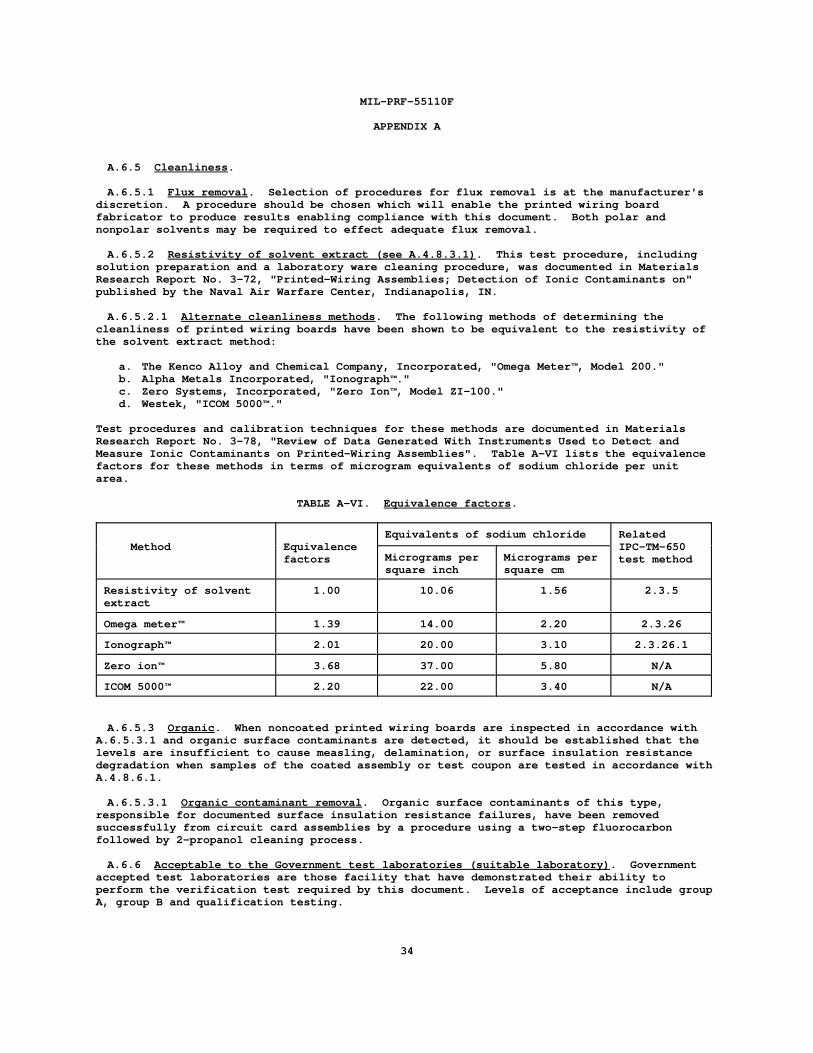
MIL-PRF-55110F
APPENDIX A
34
A.6.5 Cleanliness .
A.6.5.1 Flux removal . Selection of procedures for flux removal is at the manufacturer'sdiscretion. A procedure should be chosen which will enable the printed wiring boardfabricator to produce results enabling compliance with this document. Both polar andnonpolar solvents may be required to effect adequate flux removal.
A.6.5.2 Resistivity of solvent extract (see A.4.8.3.1) . This test procedure, includingsolution preparation and a laboratory ware cleaning procedure, was documented in MaterialsResearch Report No. 3-72, "Printed-Wiring Assemblies; Detection of Ionic Contaminants on"published by the Naval Air Warfare Center, Indianapolis, IN.
A.6.5.2.1 Alternate cleanliness methods . The following methods of determining thecleanliness of printed wiring boards have been shown to be equivalent to the resistivity ofthe solvent extract method:
a. The Kenco Alloy and Chemical Company, Incorporated, "Omega Meter™, Model 200."b. Alpha Metals Incorporated, "Ionograph™."c. Zero Systems, Incorporated, "Zero Ion™, Model ZI-100."d. Westek, "ICOM 5000™."
Test procedures and calibration techniques for these methods are documented in MaterialsResearch Report No. 3-78, "Review of Data Generated With Instruments Used to Detect andMeasure Ionic Contaminants on Printed-Wiring Assemblies". Table A-VI lists the equivalencefactors for these methods in terms of microgram equivalents of sodium chloride per unitarea.
TABLE A-VI. Equivalence factors .
Method Equivalencefactors
Equivalents of sodium chloride RelatedIPC-TM-650test methodMicrograms per
square inchMicrograms persquare cm
Resistivity of solventextract
1.00 10.06 1.56 2.3.5
Omega meter™ 1.39 14.00 2.20 2.3.26
Ionograph™ 2.01 20.00 3.10 2.3.26.1
Zero ion™ 3.68 37.00 5.80 N/A
ICOM 5000™ 2.20 22.00 3.40 N/A
A.6.5.3 Organic . When noncoated printed wiring boards are inspected in accordance withA.6.5.3.1 and organic surface contaminants are detected, it should be established that thelevels are insufficient to cause measling, delamination, or surface insulation resistancedegradation when samples of the coated assembly or test coupon are tested in accordance withA.4.8.6.1.
A.6.5.3.1 Organic contaminant removal . Organic surface contaminants of this type,responsible for documented surface insulation resistance failures, have been removedsuccessfully from circuit card assemblies by a procedure using a two-step fluorocarbonfollowed by 2-propanol cleaning process.
A.6.6 Acceptable to the Government test laboratories (suitable laboratory) . Governmentaccepted test laboratories are those facility that have demonstrated their ability toperform the verification test required by this document. Levels of acceptance include groupA, group B and qualification testing.
MIL-PRF-55110F
APPENDIX A
35
A.6.7 Alternate test methods . Other test methods may be substituted for those specifiedherein provided it is demonstrated to and approved by the qualifying activity that such asubstitution in no way relaxes the requirements of this specification.
A.6.8 Group B sample critical design details . Past non-performance versions of thisdocument contained default design details that were assumed to apply to all test couponssubjected to group B inspection, regardless of the master drawing design requirements. Withthe issuance of the performance version of this document (MIL-PRF-55110E and later), thedesign details which were universally used to determine acceptance or failure of the group Bsamples, are no longer present in this document. These needed design details are nowrelegated to the master drawing or the applicable design standard.
Therefore, additional design information, such as the critical design parameters of theprinted wiring board design (plating thickness, dielectric separation, external and internalannular ring, etc.) or the default design standard that applies to the test coupons, must besubmitted along with test coupons so that a proper group B evaluation can be completed.
Example, the master drawing of the most complex design selected for group B testingrequires .003 inch (.08 mm) of copper plating thickness, .006 inch (.15 mm) of dielectricspacing, and .005 inch (.13 mm) internal annular ring. These design details areconsiderably different than the baseline design parameters found in either IPC-D-275 orMIL-STD-275. If on these same group B samples, the laboratory acceptable to the Governmentfound that the samples exhibited .002 inch (.05 mm) of copper plating thickness, .005 inch(.13 mm) of dielectric spacing and .005 inch (.13 mm) internal annular ring, they could notstate that the results of group B testing met the specification requirement.
MIL-PRF-55110F
APPENDIX B
36
OPTIONAL QPL/QML PRODUCT ASSURANCE REQUIREMENTSFOR QUALIFIED MANUFACTURER LIST PROGRAMS
B.1. SCOPE
B.1.1 Scope . This appendix contains optional requirements concerning the QPL/QML productassurance level for printed wiring boards covered by this specification. The process forextending qualification is also outlined herein. This appendix is an optional part of thisspecification that can be used only by manufacturers qualified for listing on QML-31032. The information contained herein is intended for guidance.
B.2. APPLICABLE DOCUMENTS
B.2.1 Government specifications . The following specification forms a part of thisdocument to the extent specified herein. Unless otherwise specified, the issues of thesedocuments are those listed in the issue of the Department of Defense Index of Specificationsand Standards (DODISS) and supplement thereto, cited in the solicitation (see 6.2).
SPECIFICATIONS
DEPARTMENT OF DEFENSE
MIL-PRF-31032 - Printed Circuit Board/Printed Wiring Board, General Specification for.
(Unless otherwise indicated, copies of the above document are available from the DefensePrinting Services Detachment Office, Building 4D (Customer Services), 700 Tabor Avenue,Philadelphia, PA 19111-5094.)
B.2.2 Order of precedence . In the event of a conflict between the text of this documentand the references cited herein, the text of this document takes precedence. Nothing inthis document, however, supersedes applicable laws and regulations unless a specificexemption has been obtained.
B.3 PERFORMANCE REQUIREMENTS ISSUES
B.3.1 Performance requirements . The performance requirements of the applicableMIL-PRF-31032 associated specification shall apply to all printed wiring boards procured tothe QPL/QML product assurance level.
B.3.2 Accept/reject criteria . The accept/reject criteria of the applicable MIL-PRF-31032associated specification shall apply to all printed wiring boards procured to the QPL/QMLproduct assurance level.
B.3.3 QML brand . At the option of the manufacturer, the QML brand specified inMIL-PRF-31032 may be placed on printed wiring boards that comply with the product assurancerequirements of this appendix.
B.4 QUALIFICATIONS ISSUES
B.4.1 Reciprocal qualification (from MIL-PRF-31032) . A reciprocal qualification listing(i.e., from a technology qualified to a MIL-PRF-31032 associated specification) to thisdocument will depend on the level of QML technology qualified. Unless otherwise detailed inMIL-PRF-31032 qualification test plan, following guidelines will apply:
a. Printed board type (see A.4.5.4.1, 6.4.6 and D.3.5) . The extent of qualification forbase materials types defined in A.4.5.4 will apply. Example; a type 2 qualificationunder a MIL-PRF-31032 associated specification will not justify a type 3 qualificationlisting to this document.
MIL-PRF-55110F
APPENDIX B
37
b. Printed board material (see A.4.5.4.2) . The extent of qualification for basematerials types defined in A.4.5.4 will apply. Example; a BF base materialqualification under a MIL-PRF-31032 associated specification will justify a BF basematerial qualification listing to this document.
c. Complexity . The manufacturer can only supply QPL/QML technology equal to or less thantheir QML capability (unlike the QPL product assurance level with its unlimitedmultilayer capability qualification). Example; a type 3, 6 conductor layer GF basematerial qualification under a MIL-PRF-31032 associated specification will allow atype 3, GF base material reciprocal qualification listing to this document, however,the manufacturer could certify up to 7.5 layers as compliant (25 percent extension ofqualification as allowed by MIL-PRF-31032). In order to supply a 10 conductor layerGF base material QPL/QML printed wiring board, the QML manufacturer would need toextend its QML qualification listing. This could be done by using the add-onprovisions of MIL-PRF-31032.
B.4.1.1 Concurrent qualification . Manufacturers already qualified to the QPL level ofthis document will retain that listing after transitioning to the QPL/QML level. The 3 yearexpiration time will not apply to the QPL/QML product assurance level.
B.4.1.2 Retention (see B.6.3) . The QML status report described in MIL-PRF-31032 willcover the QPL/QML retention requirements to this document.
B.5 VERIFICATION ISSUES
B.5.1 QPL/QML product assurance . The product assurance requirements for the QPL/QML levelof printed wiring board furnished under this specification shall be satisfied bycertification to MIL-PRF-31032. All printed wiring boards manufactured and delivered incompliance with this appendix should be produced in accordance with the approved QualityManagement plan.
B.5.2 Printed wiring board performance verification . Printed wiring board performanceverification inspection shall consist of inspections on the production printed wiring boardsand test coupons specified in the applicable MIL-PRF-31032 associated specification. Thefollowing details are applicable to the QPL/QML product assurance level:
a. Lot conformance inspection (LCI) product acceptance testing should be based on theapplicable verification flows (in-process and group A) offered by this document (see4.4 and appendix D) or the routine from a similar technology described by aMIL-PRF-31032 associated specification. The various verification flows should bebased upon the design standard used to design the printed wiring boards and theavailable panel test coupons.
b. MIL-PRF-31032 periodic conformance inspection (PCI) program can be used in lieu ofgroups B inspection of this document.
c. Test optimization is applicable to this appendix and can be applied to anyverification flow detailed in this document.
B.6 NOTES
B.6.1 Intended use . This appendix is intended to be used by manufacturer's certified toMIL-PRF-31032 to reduce the complexity of maintaining multiple product/process and testingflows (both MIL-P-55110 or MIL-PRF-55110 and MIL-PRF-31032) within a the manufacturing andtesting facility.
B.6.2 Application of the QPL/QML product assurance level to existing requirements .
B.6.2.1 Use of existing master drawings . The QPL/QML printed wiring board manufacturercan use pre-existing master drawing and production artwork without any modifications(existing production masters test coupons and requires no additional or new ones).
MIL-PRF-55110F
APPENDIX B
38
B.6.2.2 Form, fit and function . The form, fit and function of the printed wiring boards,whether the QPL/QML product assurance level or the QPL product assurance level is used, willbe the same.
B.6.2.3 Certification . The printed wiring boards can be certified as being compliant tothis document (MIL-PRF-55110).
B.6.3 Benefits of the QPL/QML product assurance level . Printed wiring boards produced byQML manufacturers using the provisions of this appendix in lieu of previous revisions wouldbe compliant to this document (MIL-PRF-55110) via the QPL/QML product assurance level withthe added benefits as follows:
a. The QPL/QML manufacturer can use pre-existing master drawing and production artworkwithout any modifications needed (can use existing production masters test coupons andrequires no additional or new ones).
b. The printed wiring boards, whether the QPL/QML option or the QPL option is used, willbe the same.
c. The level of quality will be the same or higher than the QPL product assurance level.
d. When using the correct (for the design) Verification Conformance Inspection option,the cost should be the same or less due to enhancements made to accept/rejectcriteria.
e. Customers will be more confident that a QPL/QML manufacturer has demonstrated thecapabilities to build its design dues to its QML certification and qualificationrather the generic standardized qualification test vehicle of the QPL qualityassurance level portion of this document.
B.6.4 Retention issues . The manufacturer need only to keep the qualifying activityapprised of it total QML program, i.e., MIL-PRF-31032 QML and this document's QPL/QMLproduct assurance level. This means that the manufacturer does not have to maintain twoseparate compliance programs, (i.e., no need for a QPL compliance program for this documentand a QML program for MIL-PRF-31032).
B.6.5 Certificates of compliance issues . The manufacturer can certify QPL/QML printedwiring boards process under their QML program as compliant to this document. Thecertificate of compliance should reference the QPL/QML product assurance level todifferentiate the compliant product from printed wiring boards verified using the QPLproduct assurance level offered in this document.
B.6.6 Past specification revisions (see appendix D for more details) . Printed wiringboards procured to this document meets and/or exceeds all quality and reliabilityrequirements of previous revisions of MIL-P-55110 or MIL-PRF-55110.
MIL-PRF-55110F
APPENDIX C
39
C = 0 (ZERO DEFECT) SAMPLING
C.1. SCOPE
C.1.1 Scope . This appendix details the statistical sampling procedures to be used withthe QPL product assurance level of this specification. This appendix is a mandatory part ofthis specification. The information contained herein is intended for compliance.
C.2. APPLICABLE DOCUMENTS. This section is not applicable to this appendix.
C.3. DEFINITIONS AND SYMBOLS.
C.3.1 Definitions . The following definitions shall apply for all statistical samplingprocedures:
a. C = 0 sample plan: The C = 0 sample plans are defined as a combination of a testspecimen usage identifier (see b below) and a sample size series (see c below). Theresulting C = 0 sample plan will be a two character designator combination thatidentifies the sample size series that is to be with a type of test specimen for aparticular verification (see C.4.5).
b. Test specimen usage identifier: The following usage modifiers are used todifferentiate when a particular plan is to be used for a particular test specimen: (B)shall be used to identify production printed boards, (T) shall be used for testcoupons and a asterisk (*) for either printed boards or test coupons (see C.4.5 forexamples).
c. Sample size series: The sample size series is defined as the following series ofletters: B, D, F, H, J, L, and N that are listed in table C-I (see C.4.5 forexamples).
d. Tightened inspection: Tightened inspection is defined as inspection performed usingthe next sample size value in the sample size series lower than that specified.
e. Acceptance number (C): The acceptance number is defined as an integral numberassociated with the selected sample size which determines the maximum number ofdefectives permitted for that sample size.
f. Rejection number (R): Rejection number is defined as one plus the acceptance number.
C.3.2 Symbols . The following symbols shall apply for all statistical sampling procedures:
a. C: Acceptance number.
b. R: Rejection number.
C.4. STATISTICAL SAMPLING PROCEDURES AND SAMPLE PLAN TABLE
C.4.1 General . Statistical sampling shall be conducted using the C = 0 method. The C = 0method as specified herein is a sampling plan that provides a high degree of assurance thata lot having a proportion defective greater than the specified acceptance number (C = 0)will not be accepted. For all situations, the acceptance number (C) shall be equal to 0 (C= 0) and the rejection number (R) shall be 1 or greater (R � 1). For reevaluation purposes,see C.4.3.
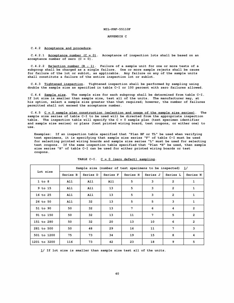
MIL-PRF-55110F
APPENDIX C
40
C.4.2 Acceptance and procedure .
C.4.2.1 Acceptance number (C = 0) . Acceptance of inspection lots shall be based on anacceptance number of zero (C = 0).
C.4.2.2 Rejection number (R � 1) . Failure of a sample unit for one or more tests of asubgroup shall be charged as a single failure. One or more sample rejects shall be causefor failure of the lot or sublot, as applicable. Any failure on any of the sample unitsshall constitute a failure of the entire inspection lot or sublot.
C.4.3 Tightened inspection . Tightened inspection shall be performed by sampling usingdouble the sample size as specified in table C-I or 100 percent with zero failures allowed.
C.4.4 Sample size . The sample size for each subgroup shall be determined from table C-I. If lot size is smaller than sample size, test all of the units. The manufacturer may, athis option, select a sample size greater than that required; however, the number of failurespermitted shall not exceed the acceptance number.
C.4.5 C = 0 sample plan construction (selection and usage of the sample size series) . Thesample size series of table C-I to be used will be directed from the appropriate inspectiontable. The inspection table will specify the C = 0 sample plan (test specimen identifierand sample size series) or plans (test printed wiring board, test coupons, or either one) touse.
Examples: If an inspection table specified that "Plan BF or TL" be used when verifyingtest specimens, it is specifying that sample size series "F" of table C-I must be usedfor selecting printed wiring boards and sample size series "L" must be used for selectingtest coupons. If the same inspection table specified that "Plan *H" be used, then samplesize series "H" of table C-I can be used for either printed wiring boards or testcoupons.
TABLE C-I. C = 0 (zero defect) sampling .
Lot sizeSample size (number of test specimens to be inspected) 1 /
Series B Series D Series F Series H Series J Series L Series N
1 to 8 All All All 5 3 2 1
9 to 15 All All 13 5 3 2 1
16 to 25 All All 13 5 3 2 1
26 to 50 All 32 13 5 5 3 1
51 to 90 50 32 13 7 6 4 2
91 to 150 50 32 13 11 7 5 2
151 to 280 50 32 20 13 10 6 2
281 to 500 50 48 29 16 11 7 3
501 to 1200 75 73 34 19 15 8 4
1201 to 3200 116 73 42 23 18 9 5
1/ If lot size is smaller than sample size test all of the units.
MIL-PRF-55110F
APPENDIX C
41
C.5. TEST EQUIPMENT AND INSPECTION FACILITIES
C.5.1 Calibration . All tests and measurements for process control, qualification testing,lot conformance inspection or periodic conformance inspection shall be made with capableinstruments whose accuracy has been verified. Calibration of measurement and test equipmentand test standards that control the accuracy of inspection and test equipment and facilitiesshall be in accordance with NCSL Z540, or equivalent.
C.5.2 Inspection facilities . The inspection facility used to perform qualificationtesting and periodic conformance inspection shall be approved by the qualifying activity forthe performance of the tests and inspection requirements of compliant printed wiring boards.
C.5.3 Acquiring activity or manufacturer imposed tests . Acquiring activity ormanufacturer imposed tests shall be in accordance with the requirements specified in themaster drawing. If any additional imposed tests detect a problem, the manufacturer shallsubmit all panels/printed wiring boards in the lot to those tests to eliminate rejects andshall take steps to determine and eliminate the cause of failure.
C.5.4 Test method alternatives . Alternate test methods are allowed provided that it isdemonstrated to the qualifying activity that such alternatives in no way relax therequirements of the test method referenced by this specification (see appendix D).
C.5.5 Procedure in case of test equipment malfunction or operator error . When it has beenestablished that a improper test is due to test equipment malfunction or operator error, theinspection facility shall document the results of its investigations and corrective actions,if required, and shall make this information available to the qualifying activity and theacquiring activity, as applicable.
MIL-PRF-55110F
APPENDIX D
42
SUPERSESSION, VERIFICATION CONFORMANCE INSPECTION OPTIONS,AND USAGE OF PAST DESIGN STANDARDS
D.1. SCOPE.
D.1.1 Scope . This appendix contains information and guidance concerning the supersessionof legacy Department of Defense documents such as MIL-P-55110 revision C, D, and E andMIL-STD-275 revision D and E. In addition, it contains the alternative VerificationConformance Inspection (VCI) options 1, 2, and 3 that have been structured around the testflows and test coupons of these legacy documents. This appendix is not a mandatory part ofthis specification. The information contained herein is intended for guidance only.
D.2. APPLICABLE DOCUMENTS. This section is not applicable to this appendix.
D.3 DEFINITIONS
D.3.1 Design standard . A document that establishes the standard practices, guidelines anddefault values for the design of printed wiring boards. Within this document, the term"design standard" is used to describe those documents that contains the design,construction, material, and test coupon requirements and guidelines.
D.3.2 Legacy designs or documents (superseded standards) . See D.4.2.
D.3.3 Supersession . The act of replacing an legacy document that no longer exists or isno longer supported with a currently supported document.
D.3.4 Verification Conformance Inspection (VCI) . A method of allowing printed wiringboards that were designed to or had test coupons applied in accordance with various legacyDepartment of Defense design standards to be tested to this document.
D.3.5 Quality conformance test circuitry . See IPC-T-50.
D.3.6 Printed wiring board types . The printed wiring board types shall be as specified ineither MIL-STD-275 and IPC-D-275. This appendix does not address design rules associatedwith printed board types 4, 5, and 6 described by IPC-D-275.
D.4 SUPERSESSION
D.4.1 Superseded specifications . Appendix A of this document includes the essentialrequirements of the previous revision and can be used to supersede the followingspecifications:
a. MIL-P-55110C, dated 26 April 1978.1. MIL-P-55110C with Amendment 1, dated 18 July 1978.2. MIL-P-55110C with Amendment 2, dated 27 August 1979.3. MIL-P-55110C with Amendment 3, dated 16 October 1980.4. MIL-P-55110C with Amendment 4, dated 28 June 1982.5. MIL-P-55110C with Amendment 5, dated 28 March 1984.
b. MIL-P-55110D, dated 31 December 1984.1. MIL-P-55110D with Amendment 1, dated 6 March 1987.2. MIL-P-55110D with Interim Amendment 2(USAF), dated 22 April 1988.3. MIL-P-55110D with Amendment 3, dated 18 May 1989.4. MIL-P-55110D with Amendment 4, dated 2 December 1990.
c. MIL-P-55110E, dated 22 December 1993.
d. MIL-PRF-55110E, dated 22 December 1993 with Amendment 1, dated 29 September 1995.
MIL-PRF-55110F
APPENDIX D
43
D.4.1.1 Reference to superseded specifications . All the requirements of this document(MIL-PRF-55110F) can be interchangeable with those of MIL-P-55110. Therefore, existingprocurement documents (master drawings or OEM documents) referencing MIL-P-55110 need not berevised, updated or changed to make reference to MIL-PRF-55110 in order for this document tobe used.
D.4.2 Superseded standards . The following design standards have been superseded byIPC-D-275.
MIL-STD-275D dated 26 April 1978.MIL-STD-275D with Notice 1 dated 19 January 1979.MIL-STD-275D with Notice 2 dated 10 October 1979.MIL-STD-275D with Notice 3 dated 5 October 1981.MIL-STD-275D with Notice 4 dated 28 May 1982.MIL-STD-275D with Notice 5 dated 7 February 1984.MIL-STD-275E dated 31 December 1984.MIL-STD-275E with Notice 1 dated 8 July 1986.
D.4.3 Testing .
D.4.3.1 Group A testing . Group A testing should be performed to the specific revision,and amendment if applicable, called out by the acquisition documents. For example, ifprinted wiring boards are produced to MIL-P-55110D with amendment 1, MIL-P-55110D withamendment 3 and MIL-P-55110E, a manufacturer would be expected to perform group A testing,for the applicable lot, to the requirements of the revision specified. In those 3 differentrevisions (D w/amendment 1, D w/amendment 3, and E) a requirement for an acceptabilitycriteria or test procedure may be the same or it might be significantly different. Retention of qualification summaries for group A should list the lots produced for each,grouped by revision and amendment.
D.4.3.1.1 Group A VCI options . The VCI options associated with group A testing arecovered in tables D-II-c, D-II-d, and D-II-e.
D.4.3.2 Group B sample selection and testing . Samples to be selected for group B testingshould be based on the most complex compliant printed wiring boards produced that month. For example, if printed wiring boards are produced to MIL-P-55110D, MIL-P-55110D withamendment 4 and MIL-PRF-55110E with amendment 1 during a given month, and the most complexprinted wiring boards produced that month were in the lot ordered to MIL-P-55110D withamendment 3, then that should be that lot from which the group B sample should be selected. The samples should be tested in accordance with MIL-P-55110D with amendment 3. If duringthat same month, printed wiring boards were produced to MIL-P-55110B and MIL-P-55110C, groupB tests to those specific revisions would also be required in order to be compliant to thoserevisions, unless specifically specified in the contract.
D.4.3.2.1 Group B VCI options . The VCI options associated with group B testing arecovered in tables D-III-c, D-III-d, and D-III-e.
D.4.3.3 Revisions . Printed wiring boards tested to this document (and using the correctVCI option) generally would meet or exceed the performance requirements of past revisions,however, due to various changes in acceptability and evaluation criteria, testing proceduresand test coupon sampling, an exact duplication of a previous revision cannot be claimed ormade in all areas of concern. Manufacturers should not pick-and-choose or mix acceptabilityrequirements and/or test procedures from one revision of MIL-P-55110 or MIL-PRF-55110 toanother. Compliance should be either to MIL-P-55110C, MIL-P-55110D, MIL-P-55110E (with aspecific amendment, if applicable) or this document entirely, unless the manufacturerdocuments a direct correlation between the revisions (with any amendments, if applicable)under consideration.
D.4.4 Updating master drawing (retooling) . Printed wiring board that were designed usingsuperseded Department of Defense design standards do not require conversion to IPC-D-275.
MIL-PRF-55110F
APPENDIX D
44
D.5 VERIFICATION CONFORMANCE OPTIONS
D.5.1 Verification flow options . The following is a general description of theVerification Conformance Inspection (VCI) Options that are available for groups A and Btesting. Unless otherwise specified, VCI option usage shall be determined using theguidelines contained in this appendix. If a VCI flow cannot be determined, use the defaultVCI flow option (VCI-4) contained in appendix A this document.
a. VCI-1: The verification flow using tables D-Id, D-IId, and D-IIId.
b. VCI-2: The verification flow using tables D-Ic, D-IIc, and D-IIIc.
c. VCI-3: The verification flow using tables D-Ib, D-IIb, and D-IIIb.
d. VCI-4: The default verification flow using tables A-II, A-III and A-IV (see appendixA of this document).
D.5.1 Verification conformance options . This document, unlike past revisions, wasdeveloped with the intent that printed wiring boards designed to various design standard(current and legacy) and various revisions of a design standard could be verified using thetesting options detailed with this document.
D.5.1.1 Description . A description of the verification conformance options are asfollows:
a. VCI Option 1 verification flow (VCI-1) uses test coupons from MIL-STD-275D and isintended to emulate the test routines of MIL-P-55110C with amendment 5.
b. VCI Option 2 verification flow (VCI-2) uses test coupons from MIL-STD-275E and isintended to emulate the test routines of MIL-P-55110D and MIL-P-55110D with amendments1, 2, or 3.
c. VCI Option 3 verification flow (VCI-3) uses test coupons from MIL-STD-275E and isintended to emulate the test routines of MIL-P-55110D with amendment 4 orMIL-P-55110E.
d. VCI Option 4 verification flow (VCI-4) uses test coupons from IPC-D-275 and is themost current testing plan for printed wiring boards.
NOTE: VCI-1 (flow 1) of this document is a close representation of the quality conformanceflow of MIL-P-55110C with amendment 5, however, because some of the accept/reject criteriawill not closely cross reference
D.6 NOTES
(This section contains information of a general or explanatory nature that may be helpful,but is not mandatory.)
D.6.1 Intended use and intent of this appendix . This appendix was developed to allow theQPL product assurance level manufacturer the option to minimize the need to maintainnumerous permutations of groups A and B test routines. These group A/B test routinesinclude all the different performance requirements, accept/reject criteria, sampling plans,and testing procedures to be used to verify pre-existing (i.e., older) printed wiring boarddesigns to a particular revision of this document. By applying this appendix and using thecorrect VCI of this document, the many permutations of reference documents, performancerequirements, accept/reject criteria, sampling schemes, and testing procedures necessary tobe entirely complaint with a previous revision of this document would not be needed.
IMPORTANT: This appendix is not a mandatory part of this specification. USE OF THISAPPENDIX IS STRICTLY OPTIONAL. This appendix was not constructed or included in thisdocument to increase the complexity or cost of testing printed wiring boards.
MIL-PRF-55110F
APPENDIX D
45
D.6.1.1 Background . The lack of supersession information or guidance regarding thechanges in test coupon quantity and usage within MIL-P-55110 and MIL-STD-275 were studied in1993 as a result of a meeting of representatives of the military services held at theDefense Electronics Supply Center on 25 March 1993 concerning procurement of printed wiringboards designed using legacy revisions of MIL-STD-275. The concept of adding multipleverification tables which emulate the group A and B testing routines of past revisions(calling out the tests and using sample sizes, test coupons, etc.) was judged the bestalternative method of all of the options studied.
D.6.2 Supporting documents . The documents in this section may be used as guidelines forthe development of a multiple Verification Conformance Inspection program and are notmandatory for this specification.
D.6.2.1 Canceled Government standards (for legacy designs) . The following canceledDepartment of Defense standard forms a part of this appendix to the extent specified herein. Unless otherwise specified, the issues of these documents are those listed in the issue ofthe Department of Defense Index of Specifications and Standards (DODISS) and supplementthereto, cited in the solicitation (see 6.2).
DEPARTMENT OF DEFENSE
MIL-STD-275 - Printed Wiring for Electronic Equipment.
(MIL-STD-275 was canceled on April 21, 1995. Unless otherwise indicated, copies of thecancellation notice are available from the Defense Printing Services Detachment Office, inPhiladelphia, PA. Copies of past revision of this standard are no longer available from theDefense Printing Services Detachment Office but might be available from other informationalservices.)
D.6.2.2 Active design standards (for current designs) . The active design standard tocurrent printed wiring board designs is IPC-D-275 "Design Standard for Rigid Printed Boardsand Rigid Printed Board Assemblies". Information concerning obtaining copies is detailed inappendix A of this document.
D.6.3 History of MIL-P-55110 and MIL-STD-275 . The method in which MIL-P-55110C,MIL-P-55110D and MIL-P-55110E were written, only particular revisions of MIL-STD-275 testcoupons could be used to test printed wiring boards tested to a particular revision ofMIL-P-55110 without complications or deviations from the specification. This made the"Superseding" statement on the first page of previous MIL-P-55110's (and MIL-STD-275 also)somewhat untrue in regards to how previous printed wiring board designs could be tested,because the revisions (55110 and its corresponding 275) were really stand alone documents(MIL-STD-275D with MIL-P-55110C and MIL-STD-275E with MIL-P-55110D and MIL-P-55110E). Thesupersession information that was necessary for the documents to transition the legacyprinted wiring board designs to the next or newer document were either ignored, left out, ornever even considered for inclusion in previous revisions of either this document or ofMIL-STD-275.
TABLE D-I. Verification Conformance Inspection (VCI) options cross reference .
VCI Option
SpecificationDesign Standard Group A table Group B table
1 MIL-P-55110C with Amendment MIL-STD-275D D-II-d D-III-c
2 MIL-P-55110D MIL-STD-275E D-II-d D-III-c
3 MIL-P-55110D with Amendment4 and MIL-P-55110E
MIL-STD-275E D-II-e D-III-e
4 Appendix A of MIL-PRF-55110 IPC-D-275 A-III A-IV
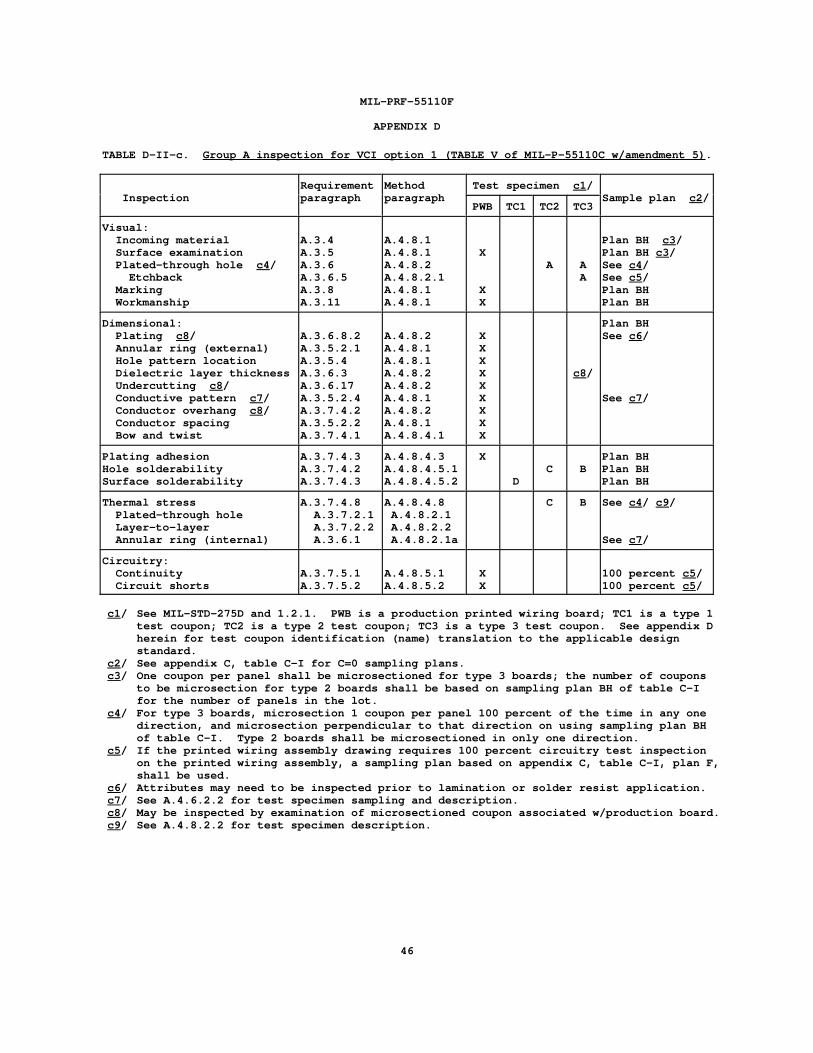
MIL-PRF-55110F
APPENDIX D
46
TABLE D-II-c. Group A inspection for VCI option 1 (TABLE V of MIL-P-55110C w/amendment 5) .
InspectionRequirementparagraph
Methodparagraph
Test specimen c1 /Sample plan c2 /
PWB TC1 TC2 TC3
Visual: Incoming material Surface examination Plated-through hole c4 / Etchback Marking Workmanship
A.3.4A.3.5A.3.6A.3.6.5A.3.8A.3.11
A.4.8.1A.4.8.1A.4.8.2A.4.8.2.1A.4.8.1A.4.8.1
X
XX
A AA
Plan BH c3 /Plan BH c3 /See c4 /See c5 /Plan BHPlan BH
Dimensional: Plating c8 / Annular ring (external) Hole pattern location Dielectric layer thickness Undercutting c8 / Conductive pattern c7 / Conductor overhang c8 / Conductor spacing Bow and twist
A.3.6.8.2A.3.5.2.1A.3.5.4A.3.6.3A.3.6.17A.3.5.2.4A.3.7.4.2A.3.5.2.2A.3.7.4.1
A.4.8.2A.4.8.1A.4.8.1A.4.8.2A.4.8.2A.4.8.1A.4.8.2A.4.8.1A.4.8.4.1
XXXXXXXXX
c8 /
Plan BHSee c6 /
See c7 /
Plating adhesionHole solderabilitySurface solderability
A.3.7.4.3A.3.7.4.2A.3.7.4.3
A.4.8.4.3A.4.8.4.5.1A.4.8.4.5.2
X
DC B
Plan BHPlan BHPlan BH
Thermal stress Plated-through hole Layer-to-layer Annular ring (internal)
A.3.7.4.8 A.3.7.2.1 A.3.7.2.2 A.3.6.1
A.4.8.4.8 A.4.8.2.1 A.4.8.2.2 A.4.8.2.1a
C B See c4 / c9 /
See c7 /
Circuitry: Continuity Circuit shorts
A.3.7.5.1A.3.7.5.2
A.4.8.5.1A.4.8.5.2
XX
100 percent c5 /100 percent c5 /
c1 / See MIL-STD-275D and 1.2.1. PWB is a production printed wiring board; TC1 is a type 1test coupon; TC2 is a type 2 test coupon; TC3 is a type 3 test coupon. See appendix Dherein for test coupon identification (name) translation to the applicable designstandard.
c2 / See appendix C, table C-I for C=0 sampling plans.c3 / One coupon per panel shall be microsectioned for type 3 boards; the number of coupons
to be microsection for type 2 boards shall be based on sampling plan BH of table C-Ifor the number of panels in the lot.
c4 / For type 3 boards, microsection 1 coupon per panel 100 percent of the time in any onedirection, and microsection perpendicular to that direction on using sampling plan BHof table C-I. Type 2 boards shall be microsectioned in only one direction.
c5 / If the printed wiring assembly drawing requires 100 percent circuitry test inspectionon the printed wiring assembly, a sampling plan based on appendix C, table C-I, plan F,shall be used.
c6 / Attributes may need to be inspected prior to lamination or solder resist application.c7 / See A.4.6.2.2 for test specimen sampling and description.c8 / May be inspected by examination of microsectioned coupon associated w/production board.c9 / See A.4.8.2.2 for test specimen description.
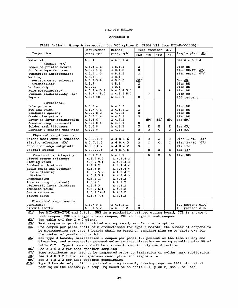
MIL-PRF-55110F
APPENDIX D
47
TABLE D-II-d. Group A inspection for VCI option 2 (TABLE VII from MIL-P-55110D) .
InspectionRequirementparagraph
Methodparagraph
Test specimen d1 /Sample plan d2 /
PWB TC1 TC2 TC3
MaterialVisual: d7 /
Edges of printed boards Surface imperfections Subsurface imperfections Marking Resistance to solvents Traceability Workmanship Hole solderability Surface solderability d3 / Repair
A.3.4
A.3.5.1.1A.3.5.1.2A.3.5.1.3A.3.8A.3.7.3.2A.3.9A.3.11A.3.7.4.5.1A.3.7.4.5.2A.3.7.10
A.4.6.1.4
4.8.1.14.8.1.24.8.1.34.8.14.8.3.24.8.14.8.1A.4.8.4.5.1A.4.8.4.5.2A.4.8.1
XXX
d8/XX
XC
A A
See A.4.6.1.4
Plan BHPlan BH/TJ d7 /Plan BH/TJ d7 /
See d8 /Plan BHPlan BHPlan BHPlan BH100 percent
Dimensional: Hole pattern Bow and twist Conductor spacing Conductive pattern Layer �to �layer registration Annular ring (external) Solder mask thickness Plating & coating thickness
A.3.5.4A.3.7.4.1A.3.5.2.2A.3.5.2.4A.3.5.6A.3.5.2.1A.3.5.8A.3.6.8
A.4.8.2A.4.8.4.1A.4.8.1A.4.8.1A.4.8.1A.4.8.1A.4.8.1A.4.8.2
XXXX
XXX
d9/
EC
d9/
EC
d9/
EC
Plan BHPlan BHPlan BHPlan BHSee d9 /
See d3 /See d3 /
Physical requirements:Solder mask cure & adhesionPlating adhesion d3 / Conductor edge outgrowthThermal stress
A.3.7.4.6A.3.7.4.3A.3.7.4.2A.3.7.4.8
A.4.8.4.6A.4.8.4.3A.4.8.4.2A.4.8.4.8
XXX
JC
B
JC
B
JC
B
Plan BH/TJ d3 /Plan BH/TJ d7 /Plan BHSee d6 /
Construction integrity:Plated copper thicknessPlating voidsConductor thicknessResin smear and etchback Hole cleaning EtchbackUndercuttingAnnular ring (internal)Dielectric layer thicknessLaminate voidsResin recessionLifted lands
A.3.7.2.1 A.3.6.8.2 A.3.6.9.1 A.3.6.2 A.3.6.5 A.3.6.5.2 A.3.6.5.1 A.3.6.17 A.3.6.1 A.3.6.3 A.3.6.6.1 A.3.6.14.1 A.3.6.7.1
A.4.8.2 A.4.8.4.2 A.4.8.4.3 A.4.8.4.4 A.4.8.4.6 A.4.8.4.7 A.4.8.4.9 A.4.8.2 A.4.8.2 A.4.8.2 A.4.8.2 A.4.8.2 A.4.8.2
B B B Plan BH*
Electrical requirements:ContinuityCircuit shorts
A.3.7.5.1A.3.7.5.2
A.4.8.5.1A.4.8.5.2
XX
100 percent d10 /100 percent d10 /
d1/ See MIL-STD-275E and 1.2.1. PWB is a production printed wiring board; TC1 is a type 1test coupon; TC2 is a type 2 test coupon; TC3 is a type 3 test coupon.
d2/ See table C-I for C = 0 plans.d3/ Test coupon or production printed wiring board, manufacturer's option.d4/ One coupon per panel shall be microsectioned for type 3 boards; the number of coupons to
be microsection for type 2 boards shall be based on sampling plan BH of table C-I forthe number of panels in the lot.
d5/ For type 3 boards, microsection 1 coupon per panel 100 percent of the time in any onedirection, and microsection perpendicular to that direction on using sampling plan BH oftable C-I. Type 2 boards shall be microsectioned in only one direction.
d6/ See A.4.6.2.2 for test specimen sampling.d7/ Some attributes may need to be inspected prior to lamination or solder mask application.d8/ See A.4.8.3.2.1 for test specimen description and sample size.d9/ See A.4.8.2.2 for test specimen description.
d10 / Type 3 boards only. If the printed wiring assembly drawing requires 100% electricaltesting on the assembly, a sampling based on an table C-I, plan F, shall be used.
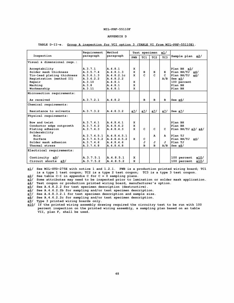
MIL-PRF-55110F
APPENDIX D
48
TABLE D-II-e. Group A inspection for VCI option 3 (TABLE VI from MIL-PRF-55110E) .
InspectionRequirementparagraph
Methodparagraph
Test specimen e1 /Sample plan e2 /PWB TC1 TC2 TC3
Visual & dimensional reqs.:
Acceptability Solder mask thickness Tin-lead plating thickness Registration (method II) Repair Marking Workmanship
A.3.7.1A.3.5.7.4A.3.6.1.3A.3.6.2.2A.3.10A.3.8A.3.11
A.4.8.1A.4.8.1.3A.4.8.2.1cA.4.8.2.2A.4.8.1A.4.8.1A.4.8.1
XXX
XXX
EC
EC
EC
A/B
Plan BH e3 /Plan BH/TJ e4 /Plan BH/TJ e4 /See e5 /100 percentPlan BHPlan BH
Microsection requirements:
As received A.3.7.2.1 A.4.8.2 B B B See e6 /
Chemical requirements:
Resistance to solvents A.3.7.3.2 A.4.8.3.2 e7 / e7 / e7 / e7 / See e7 /
Physical requirements:
Bow and twist Conductor edge outgrowth Plating adhesion Solderability Hole Surface Solder mask adhesion Thermal stress
A.3.7.4.1A.3.7.4.2A.3.7.4.3
A.3.7.4.5.1A.3.7.4.5.2A.3.7.4.6A.3.7.4.8
A.4.8.4.1A.4.8.4.2A.4.8.4.3
A.4.8.4.5.1A.4.8.4.5.2A.4.8.4.6A.4.8.4.8
XXX
X
C
CJB
C
A
JB
C
A
JA/B
Plan BHPlan BHPlan BH/TJ e3 / e4 /
Plan TJPlan BH/TJ e4 /Plan TJSee e8 /
Electrical requirements:
Continuity e9 / Circuit shorts e9 /
A.3.7.5.1A.3.7.5.2
A.4.8.5.1A.4.8.5.2
XX
100 percent e10 /100 percent e10 /
e1/ See MIL-STD-275E with notice 1 and 1.2.1. PWB is a production printed wiring board; TC1is a type 1 test coupon; TC2 is a type 2 test coupon; TC3 is a type 3 test coupon.
e2/ See table C-I in appendix C for C = 0 sampling plans.e3/ Some attributes may need to be inspected prior to lamination or solder mask application.e4/ Test coupon or production printed wiring board, manufacturer's option.e5/ See A.4.8.2.2 for test specimen description (destructive).e6/ See A.4.6.2.2b for sampling and/or test specimen description.e7/ See A.4.8.3.2.1 for test specimen description and sample size.e8/ See A.4.6.2.2c for sampling and/or test specimen description.e9/ Type 3 printed wiring boards only.e10 / If the printed wiring assembly drawing required the circuitry test to be run with 100
percent inspection on the printed wiring assembly, a sampling plan based on an tableVII, plan F, shall be used.
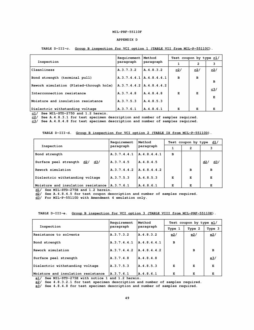
MIL-PRF-55110F
APPENDIX D
49
TABLE D-III-c. Group B inspection for VCI option 1 (TABLE VII from MIL-P-55110C ).
InspectionRequirementparagraph
Methodparagraph
Test coupon by type c1 /
1 2 3
Cleanliness
Bond strength (terminal pull)
Rework simulation (Plated-through hole)
Interconnection resistance
Moisture and insulation resistance
Dielectric withstanding voltage
A.3.7.3.2
A.3.7.4.4.1
A.3.7.4.4.2
A.3.7.4.8
A.3.7.5.3
A.3.7.6.1
A.4.8.3.2
A.4.8.4.4.1
A.4.8.4.4.2
A.4.8.4.8
A.4.8.5.3
A.4.8.6.1
c2 /
B
E
E
c2 /
B
E
E
c2 /
B
c3 /
E
Ec1 / See MIL-STD-275D and 1.2 herein.c2 / See A.4.8.3.1 for test specimen description and number of samples required.c3 / See A.4.8.4.8 for test specimen description and number of samples required.
TABLE D-III-d. Group B inspection for VCI option 2 (TABLE IX from MIL-P-55110D ).
InspectionRequirementparagraph
Methodparagraph
Test coupon by type d1 /
1 2 3
Bond strength
Surface peel strength d2 / d3 /
Rework simulation
Dielectric withstanding voltage
Moisture and insulation resistance
A.3.7.4.4.1
A.3.7.4.5
A.3.7.4.4.2
A.3.7.5.3
A.3.7.6.1
A.4.8.4.4.1
A.4.8.4.5
A.4.8.4.4.2
A.4.8.5.3
A.4.8.6.1
B
E
E
B
E
E
d2/ d3 /
B
E
Ed1/ See MIL �STD�275E and 1.2 herein.d2/ See A.4.8.4.5 for test coupon description and number of samples required.d3/ For MIL-P-55110D with Amendment 4 emulation only.
TABLE D-III-e. Group B inspection for VCI option 3 (TABLE VIII from MIL-PRF-55110E ).
InspectionRequirementparagraph
Methodparagraph
Test coupon by type e1 /
Type 1 Type 2 Type 3
Resistance to solvents
Bond strength
Rework simulation
Surface peel strength
Dielectric withstanding voltage
Moisture and insulation resistance
A.3.7.3.2
A.3.7.4.4.1
A.3.7.4.4.2
A.3.7.4.8
A.3.7.5.3
A.3.7.6.1
A.4.8.3.2
A.4.8.4.4.1
A.4.8.4.4.2
A.4.8.4.8
A.4.8.5.3
A.4.8.6.1
e2/
B
E
E
e2/
B
E
E
e2/
B
e3/
E
Ee1/ See MIL-STD-275E with notice 1 and 1.2 herein.e2/ See 4.8.3.2.1 for test specimen description and number of samples required.e3/ See 4.8.4.8 for test specimen description and number of samples required.
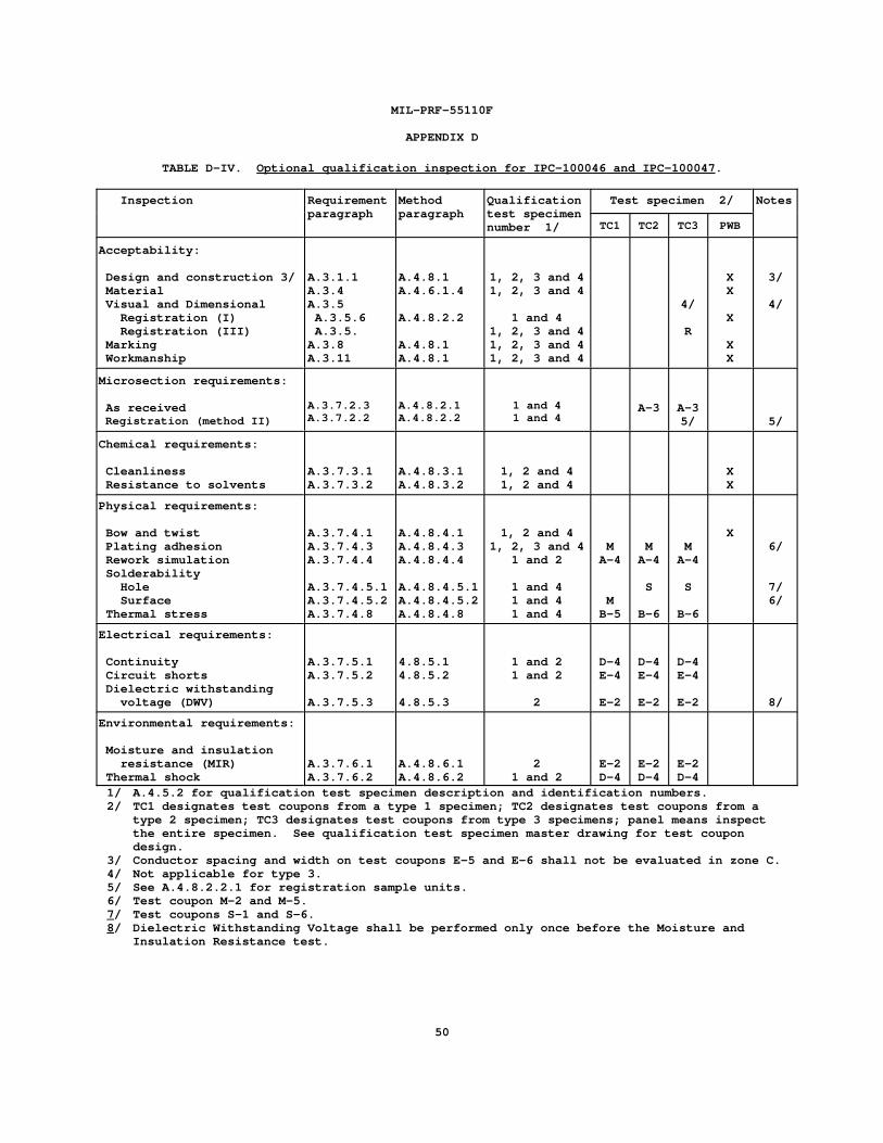
MIL-PRF-55110F
APPENDIX D
50
TABLE D-IV. Optional qualification inspection for IPC-100046 and IPC-100047 .
Inspection Requirementparagraph
Methodparagraph
Qualificationtest specimennumber 1/
Test specimen 2/ Notes
TC1 TC2 TC3 PWB
Acceptability:
Design and construction 3/ Material Visual and Dimensional Registration (I) Registration (III) Marking Workmanship
A.3.1.1A.3.4A.3.5 A.3.5.6 A.3.5.A.3.8A.3.11
A.4.8.1A.4.6.1.4
A.4.8.2.2
A.4.8.1A.4.8.1
1, 2, 3 and 41, 2, 3 and 4
1 and 41, 2, 3 and 41, 2, 3 and 41, 2, 3 and 4
4/
R
XX
X
XX
3/
4/
Microsection requirements:
As received Registration (method II)
A.3.7.2.3A.3.7.2.2
A.4.8.2.1A.4.8.2.2
1 and 41 and 4
A-3 A-35/ 5/
Chemical requirements:
Cleanliness Resistance to solvents
A.3.7.3.1A.3.7.3.2
A.4.8.3.1A.4.8.3.2
1, 2 and 41, 2 and 4
XX
Physical requirements:
Bow and twist Plating adhesion Rework simulation Solderability Hole Surface Thermal stress
A.3.7.4.1A.3.7.4.3A.3.7.4.4
A.3.7.4.5.1A.3.7.4.5.2A.3.7.4.8
A.4.8.4.1A.4.8.4.3A.4.8.4.4
A.4.8.4.5.1A.4.8.4.5.2A.4.8.4.8
1, 2 and 41, 2, 3 and 4
1 and 2
1 and 41 and 41 and 4
MA-4
MB-5
MA-4
S
B-6
MA-4
S
B-6
X6/
7/6/
Electrical requirements:
Continuity Circuit shorts Dielectric withstanding voltage (DWV)
A.3.7.5.1A.3.7.5.2
A.3.7.5.3
4.8.5.14.8.5.2
4.8.5.3
1 and 21 and 2
2
D-4E-4
E-2
D-4E-4
E-2
D-4E-4
E-2 8/
Environmental requirements:
Moisture and insulation resistance (MIR) Thermal shock
A.3.7.6.1A.3.7.6.2
A.4.8.6.1A.4.8.6.2
21 and 2
E-2D-4
E-2D-4
E-2D-4
1/ A.4.5.2 for qualification test specimen description and identification numbers.2/ TC1 designates test coupons from a type 1 specimen; TC2 designates test coupons from a
type 2 specimen; TC3 designates test coupons from type 3 specimens; panel means inspectthe entire specimen. See qualification test specimen master drawing for test coupondesign.
3/ Conductor spacing and width on test coupons E-5 and E-6 shall not be evaluated in zone C.4/ Not applicable for type 3.5/ See A.4.8.2.2.1 for registration sample units.6/ Test coupon M-2 and M-5.7/ Test coupons S-1 and S-6.8/ Dielectric Withstanding Voltage shall be performed only once before the Moisture and
Insulation Resistance test.
MIL-PRF-55110F
APPENDIX E
51
SEQUENTIAL ELECTROCHEMICAL REDUCTION ANALYSIS (SERA)SOLDERABILITY TEST
E.1. SCOPE.
E.1.1 Scope . This test method describes the method and procedure used to evaluateoxidation levels on solderable surfaces. The type and quantity of oxides on copper, tin,and lead surfaces have a significant impact on solderability. The procedure involves usingelectrochemical reduction techniques to determine the type and quantity of oxide onplated-through holes, attachment lands, and printed wiring board surface conductors. TheSERA solderability test method is offered as an alternative to other solderability testmethods required by this document. This test method shall not be contractually imposed uponeither the contractor or sub-contractor. This appendix is not a mandatory part of thespecification. The information contained herein is intended for compliance only whenvolunteered as an alternative to the other solderability test methods detailed.
E.2. APPLICABLE DOCUMENTS.
E.2.1 Government documents .
E.2.1.1 Specifications . The following specifications form a part of this document to theextent specified herein. Unless otherwise specified, the issues of these documents arethose listed in the issue of the Department of Defense Index of Specifications and Standards(DODISS) and supplement thereto, cited in the solicitation (see 6.2).
SPECIFICATIONS
FEDERAL
O-C-265 - Chemicals, Analytical; General Specification for.
(Unless otherwise indicated, copies of federal specifications are available from theStandardization Documents Order Desk, Building 4D, 700 Robbins Avenue, Philadelphia, PA 19111-5094.)
E.2.2 Non-Government publications . The following documents form a part of thisspecification to the extent specified herein. Unless otherwise specified, the issues of thedocuments which are DoD adopted are those listed in the issue of the DODISS cited in thesolicitation. Unless otherwise specified, the issues of documents not listed in the DODISSare the issue of the documents cited in the solicitation (see 6.2).
INSTITUTE FOR INTERCONNECTING AND PACKAGING ELECTRONIC CIRCUITS (IPC)
J-STD-004 - Requirements for Soldering Fluxes.
(Application for copies should be addressed to the Institute for Interconnecting andPackaging Electronic Circuits, 2215 Sanders Road, Northbrook, IL 60062-6135.)
(Non-Government standards and other publications are normally available from theorganizations that prepare or distribute the documents. These documents also may beavailable in or through libraries or other informational services.)
E.2.3 Order of precedence . In the event of a conflict between the text of this documentand the references cited herein, the text of this document takes precedence. Nothing inthis document, however, supersedes applicable laws and regulations unless a specificexemption has been obtained.
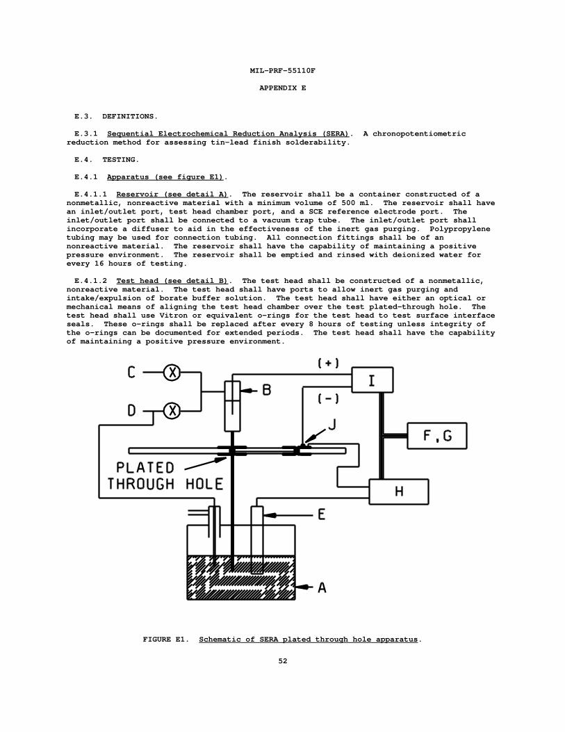
MIL-PRF-55110F
APPENDIX E
52
E.3. DEFINITIONS.
E.3.1 Sequential Electrochemical Reduction Analysis (SERA) . A chronopotentiometricreduction method for assessing tin-lead finish solderability.
E.4. TESTING.
E.4.1 Apparatus (see figure E1) .
E.4.1.1 Reservoir (see detail A) . The reservoir shall be a container constructed of anonmetallic, nonreactive material with a minimum volume of 500 ml. The reservoir shall havean inlet/outlet port, test head chamber port, and a SCE reference electrode port. Theinlet/outlet port shall be connected to a vacuum trap tube. The inlet/outlet port shallincorporate a diffuser to aid in the effectiveness of the inert gas purging. Polypropylenetubing may be used for connection tubing. All connection fittings shall be of annonreactive material. The reservoir shall have the capability of maintaining a positivepressure environment. The reservoir shall be emptied and rinsed with deionized water forevery 16 hours of testing.
E.4.1.2 Test head (see detail B) . The test head shall be constructed of a nonmetallic,nonreactive material. The test head shall have ports to allow inert gas purging andintake/expulsion of borate buffer solution. The test head shall have either an optical ormechanical means of aligning the test head chamber over the test plated-through hole. Thetest head shall use Vitron or equivalent o-rings for the test head to test surface interfaceseals. These o-rings shall be replaced after every 8 hours of testing unless integrity ofthe o-rings can be documented for extended periods. The test head shall have the capabilityof maintaining a positive pressure environment.
FIGURE E1. Schematic of SERA plated through hole apparatus .
MIL-PRF-55110F
APPENDIX E
53
E.4.1.3 Vacuum pump (see detail C) . A vacuum pump shall be used to draw buffer solutioninto and out of the test head compartment. The vacuum pump shall be able to draw minimumvacuum of 5 inches of Hg (15 kPa).
E.4.1.4 Gas regulator (see detail D) . An in-line gas regulator shall be used to monitorthe flow of the inert purging gas. The gas regulator shall be able to measure a minimum of1 cubic foot per hour (0.02832 cubic meters per hour) at standard temperature and pressure.
E.4.1.5 SCE reference electrode (see detail E) . The reference electrode shall be asaturated calomel electrode (SCE) with a temperature range of -5 (C to +60 (C and a Ph range of0-14. The SCE reference electrode shall be stored in such a manner as to prevent drying out(either in a saturated KCI solution or in accordance with the manufacturer's instructions). The SCE reference electrode shall be calibrated in accordance with the manufacturer'sinstructions once every 30 days.
E.4.1.6 Computer (see detail F) . The computer shall be equivalent to or better than aMS-DOS compatible, 80286-12MHz, with 512 Kbyte of internal memory and floppy and hard diskdrives.
E.4.1.7 IEEE-488 interface card (see detail G) . An IEEE-488 interface card is requiredfor data acquisition between the computer, the digital multimeter, and the programmablecurrent source.
E.4.1.8 Digital multimeter (see detail H) . A digital multimeter is required to measurethe voltage changes during the SERA reduction. The digital multimeter shall have thefollowing characteristics:
a. A measurable voltage range of 0 V to -2.0 V.
b. A voltage measurement tolerance of ±5 mV.
c. Voltage measurement RMS noise level should not exceed 10 Mv.
d. Input impedance should be greater than 1 G-Ohm.
E.4.1.9 Programmable current source (see detail I) . A programmable current source isrequired to apply a constant current during the SERA reduction. The programmable currentsource shall have the following minimum characteristics:
a. The applied current should be variable in 0.1 µamp steps between 1.0 µamps and 10µamps.
b. The applied current should remain constant within ±5 percent.
E.4.1.10 Printed wiring board (PWB) contact pin (see detail J) . A contact pin is requiredto complete the electrical circuit with the test plated-through hole. The contact pin shallnot exert a force of greater than .5 pounds (0.23 Kg) nor alter the plated-through holeform, fit, or function.
E.4.2 Materials .
E.4.2.1 Borate buffer solution . The SERA test requires the use of a borate buffersolution. This solution uses reagent grade boric acid, sodium borate (N a B 0 *10 H 0), and2 4 7 2
deionized water. The recipe is 6.18 grams/liter boric acid and 9.55 grams/liter of sodiumborate. The Ph of the borate buffer solution shall range in the range of 8.3 to 8.4. Adjustments to the buffer Ph shall be made using either boric acid or sodium borateadditions.
E.4.2.2 Inert gas . An inert gas is required to purge oxygen from the system. Eitherargon or ultra high purity (99.998%) dry nitrogen shall be used.
E.4.2.3 Deionized water . Deionized water comprises a portion of the borate buffersolution and shall be used to rinse the test plated-through hole after completion of theSERA analysis. The deionized water shall be 1 Megohm conductivity or better.
MIL-PRF-55110F
APPENDIX E
54
E.4.2.4 Isopropyl alcohol . Isopropyl alcohol is used to rinse the test plated-throughhole after the competition of the SERA analysis. Reagent grade isopropyl alcohol, inaccordance with O-C-265, shall be used.
E.4.2.5 Potassium chloride solution (KCI) . The SCE reference electrode may be stored in asaturated KCI solution. This solution uses reagent grade potassium chloride, in accordancewith O-C-265, in a saturated solution form.
E.5. PROCEDURES.
E.5.1 General . The test procedure shall be performed on three plated-through holesrandomly chosen on the printed wiring board or representative test coupon. The SERA testshall be performed just prior to packaging for storage or shipment or immediately uponremoval from the manufacturer's protective package. During handling, care shall beexercised to prevent the surfaces being tested from being abraded or contaminated by grease,perspirants, abnormal atmosphere, etc. The test procedure consists of the followingoperations:
a. Proper preparation of SERA system (See B.5.2).
b. Application of test method (see B.5.3).
c. Evaluation of test data (see B.5.4).
d. Proper post test preparation of SERA system (see B.5.5).
E.5.2 Preparation of SERA systems .
a. Initiate inert gas flow into system and allow a minimum of 10 minutes to elapse priorto testing.
b. Turn on digital multimeter and programmable current source and allow a minimum of 10minutes to elapse prior to testing.
c. Remove reference electrode port and rinse with deionized water. Replace referenceelectrode port and add sufficient quantity of borate buffer solution to immerse theSCE reference electrode a minimum of 1 inch (25.4 mm).
d. Remove SCE reference electrode from storage container. Rinse with deionized water,wipe with clean soft cloth, and place into reference electrode port. Attach systemelectrical connections in accordance with figure E1.
e. Remove and replace test head o-ring seals as required (see B.4.1.2).
f. Close SERA test head together thus seating o-rings together on a representative sampleplated-through hole and perform vacuum check on system. No visible air bubbles shallbe detected in the test head chamber which would indicate improper sealing.
E.5.3 Application of test method .
a. The test operator shall record the specimen lot date code and manufacturer for eachindividual printed wiring board. An individual printed wiring board reference chartfor the test plated-through holes and PWB contact pin locations shall be maintainedfor each test specimen configuration.
b. Insert test specimen onto SERA test head and allow a minimum of 4 seconds for inertgas purging of the test head. Ensure inert gas bubbling is occurring in the reservoirtube.
c. Attach PWB contact pin.
d. Attach electrical source leads.
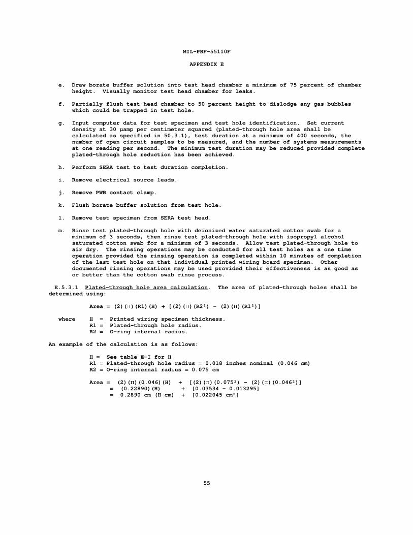
MIL-PRF-55110F
APPENDIX E
55
e. Draw borate buffer solution into test head chamber a minimum of 75 percent of chamberheight. Visually monitor test head chamber for leaks.
f. Partially flush test head chamber to 50 percent height to dislodge any gas bubbleswhich could be trapped in test hole.
g. Input computer data for test specimen and test hole identification. Set currentdensity at 30 µamp per centimeter squared (plated-through hole area shall becalculated as specified in 50.3.1), test duration at a minimum of 400 seconds, thenumber of open circuit samples to be measured, and the number of systems measurementsat one reading per second. The minimum test duration may be reduced provided completeplated-through hole reduction has been achieved.
h. Perform SERA test to test duration completion.
i. Remove electrical source leads.
j. Remove PWB contact clamp.
k. Flush borate buffer solution from test hole.
l. Remove test specimen from SERA test head.
m. Rinse test plated-through hole with deionized water saturated cotton swab for aminimum of 3 seconds, then rinse test plated-through hole with isopropyl alcoholsaturated cotton swab for a minimum of 3 seconds. Allow test plated-through hole toair dry. The rinsing operations may be conducted for all test holes as a one timeoperation provided the rinsing operation is completed within 10 minutes of completionof the last test hole on that individual printed wiring board specimen. Otherdocumented rinsing operations may be used provided their effectiveness is as good asor better than the cotton swab rinse process.
E.5.3.1 Plated-through hole area calculation . The area of plated-through holes shall bedetermined using:
Area = (2)( %)(R1)(H) + [(2)( %)(R2²) - (2)( %)(R1²)]
where H = Printed wiring specimen thickness.R1 = Plated-through hole radius.R2 = O-ring internal radius.
An example of the calculation is as follows:
H = See table E-I for HR1 = Plated-through hole radius = 0.018 inches nominal (0.046 cm)R2 = O-ring internal radius = 0.075 cm
Area = (2)( %)(0.046)(H) + [(2)( %)(0.075²) - (2)( %)(0.046²)]= (0.22890)(H) + [0.03534 - 0.013295]= 0.2890 cm (H cm) + [0.022045 cm²]
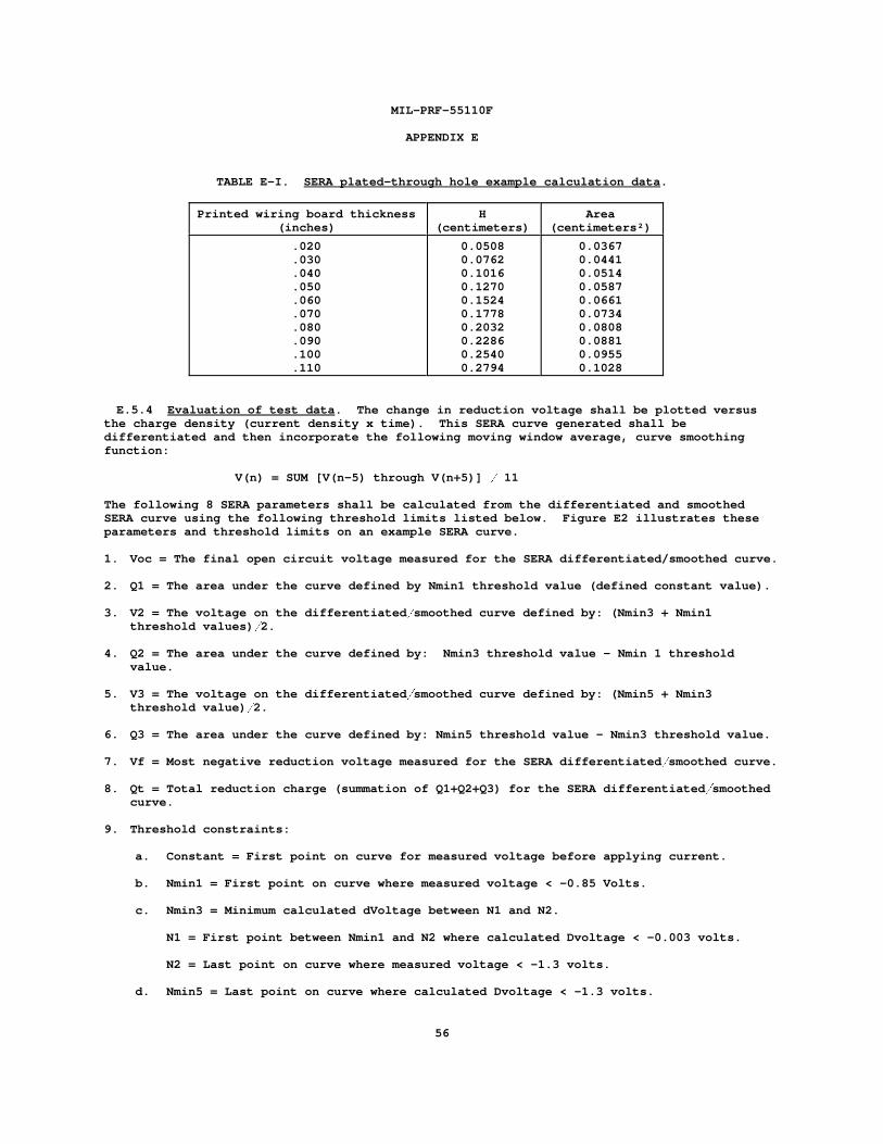
MIL-PRF-55110F
APPENDIX E
56
TABLE E-I. SERA plated-through hole example calculation data .
Printed wiring board thickness(inches)
H(centimeters)
Area(centimeters²)
.020
.030
.040
.050
.060
.070
.080
.090
.100
.110
0.05080.07620.10160.12700.15240.17780.20320.22860.25400.2794
0.03670.04410.05140.05870.06610.07340.08080.08810.09550.1028
E.5.4 Evaluation of test data . The change in reduction voltage shall be plotted versusthe charge density (current density x time). This SERA curve generated shall bedifferentiated and then incorporate the following moving window average, curve smoothingfunction:
V(n) = SUM [V(n-5) through V(n+5)] 11
The following 8 SERA parameters shall be calculated from the differentiated and smoothedSERA curve using the following threshold limits listed below. Figure E2 illustrates theseparameters and threshold limits on an example SERA curve.
1. Voc = The final open circuit voltage measured for the SERA differentiated/smoothed curve.
2. Q1 = The area under the curve defined by Nmin1 threshold value (defined constant value).
3. V2 = The voltage on the differentiated smoothed curve defined by: (Nmin3 + Nmin1threshold values) 2.
4. Q2 = The area under the curve defined by: Nmin3 threshold value - Nmin 1 thresholdvalue.
5. V3 = The voltage on the differentiated smoothed curve defined by: (Nmin5 + Nmin3threshold value) 2.
6. Q3 = The area under the curve defined by: Nmin5 threshold value - Nmin3 threshold value.
7. Vf = Most negative reduction voltage measured for the SERA differentiated smoothed curve.
8. Qt = Total reduction charge (summation of Q1+Q2+Q3) for the SERA differentiated smoothedcurve.
9. Threshold constraints:
a. Constant = First point on curve for measured voltage before applying current.
b. Nmin1 = First point on curve where measured voltage < -0.85 Volts.
c. Nmin3 = Minimum calculated dVoltage between N1 and N2.
N1 = First point between Nmin1 and N2 where calculated Dvoltage < -0.003 volts.
N2 = Last point on curve where measured voltage < -1.3 volts.
d. Nmin5 = Last point on curve where calculated Dvoltage < -1.3 volts.
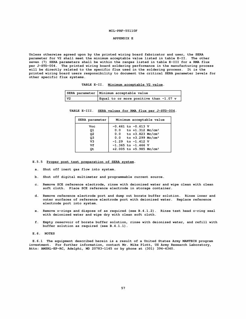
MIL-PRF-55110F
APPENDIX E
57
Unless otherwise agreed upon by the printed wiring board fabricator and user, the SERAparameter for V2 shall meet the minimum acceptable value listed in table E-II. The otherseven (7) SERA parameters shall be within the ranges listed in table E-III for a RMA fluxper J-STD-004. The printed wiring board soldering performance in the manufacturing processwill be directly related to the specific flux used in the soldering process. It is theprinted wiring board users responsibility to document the critical SERA parameter levels forother specific flux systems.
TABLE E-II. Minimum acceptable V2 value .
SERA parameter Minimum acceptable value
V2 Equal to or more positive than -1.07 v
TABLE E-III. SERA values for RMA flux per J-STD-004 .
SERA parameter Minimum acceptable value
VocQ1Q2Q3V3VfQt
-0.461 to -0.613 V 0.0 to +1.312 Mc/cm² 0.0 to +3.823 Mc/cm² 0.0 to +3.299 Mc/cm² -1.29 to -1.412 V -1.365 to -1.466 V +2.005 to +5.985 Mc/cm²
E.5.5 Proper post test preparation of SERA system .
a. Shut off inert gas flow into system.
b. Shut off digital multimeter and programmable current source.
c. Remove SCE reference electrode, rinse with deionized water and wipe clean with cleansoft cloth. Place SCE reference electrode in storage container.
d. Remove reference electrode port and dump out borate buffer solution. Rinse inner andouter surfaces of reference electrode port with deionized water. Replace referenceelectrode port into system.
e. Remove o-rings and dispose of as required (see B.4.1.2). Rinse test head o-ring sealwith deionized water and wipe dry with clean soft cloth.
f. Empty reservoir of borate buffer solution, rinse with deionized water, and refill withbuffer solution as required (see B.4.1.1).
E.6. NOTES
E.6.1 The equipment described herein is a result of a United States Army MANTECH programinvestment. For further information, contact Mr. Mike Plott, US Army Research Laboratory,Attn: AMSRL-EP-RC, Adelphi, MD 20783-1145 or by phone at (301) 394-4340.
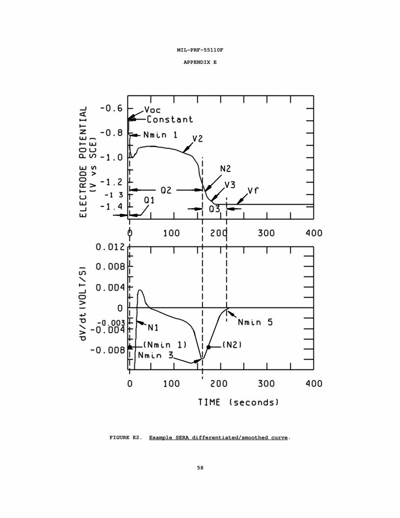
MIL-PRF-55110F
APPENDIX E
58
FIGURE E2. Example SERA differentiated/smoothed curve .
MIL-PRF-55110F
59
CONCLUDING MATERIAL
Custodians: Preparing activity:Army - CR DLA - CCNavy - ECAir Force - 85 (Project 5998-0083)
Review activities:Army - AR, MINavy - AS, CG, MC, OS, SH, TDAir Force - 11, 16, 17, 19, 99NSA - NS
STANDARDIZATION DOCUMENT IMPROVEMENT PROPOSAL
INSTRUCTIONS
1. The preparing activity must complete blocks 1, 2, 3, and 8. In block 1, both the document number and revision letter should be given.
2. The submitter of this form must complete blocks 4, 5, 6, and 7.
3. The preparing activity must provide a reply within 30 days from receipt of the form.
NOTE: This form may not be used to request copies of documents, nor to request waivers, orclarification of requirements on current contracts. Comments submitted on this form do not constituteor imply authorization to waive any portion of the referenced document(s) or to amend contractualrequirements.
I RECOMMEND A CHANGE: 1. DOCUMENT NUMBER MIL-PRF-55110F
2. DOCUMENT DATE (YYMMDD) 97-05-31
3. DOCUMENT TITLE: PRINTED WIRING BOARD, RIGID, GENERAL SPECIFICATION FOR
4. NATURE OF CHANGE (Identify paragraph number and include proposed rewrite, if possible. Attachextra sheets as needed.)
5. REASON FOR RECOMMENDATION
6. SUBMITTER
a. NAME (Last, First, Middleinitial)
b. ORGANIZATION
c. ADDRESS (Include Zip Code) d. TELEPHONE (Include AreaCode)
(1) Commercial
(2) AUTOVON (If applicable)
7. DATE SUBMITTED (YYMMDD)
8. PREPARING ACTIVITY
a. NAME David Corbett [email protected]
b. TELEPHONE (Include Area Code)(1) Commercial (614) 692-0526 (2) AUTOVON 850-0526 URL http://www.dscc.dla.mil/V/VA/VAC
c. ADDRESS (Include Zip Code) DSCC-VAC 3990 East Broad Street Columbus, OH 43213-1152
IF YOU DO NOT RECEIVE A REPLY WITHIN 45 DAYS, CONTACT: Defense Quality and Standardization Office 5203 Leesburg Pike, Suite 1403, Falls Church, VA 22041-3466 Telephone (703) 756-2340 AUTOVON 289-2340
DD Form 1426, OCT 89 Previous editions are obsolete 198/290