Improvement of New Automotive Power Semiconductor Packages · LPE technology uses conventional...
44
AUTOMOTIVE POWER Improvement of New Automotive Power Semiconductor Packages ISSUE 1 – JANUARY/FEBRUARY 2010 Also inside this issue Opinion | Market News | Events | Energy Harvesting | Renewable Power | Battery Monitoring | Power Modules | Power Diodes | Website Locator
Transcript of Improvement of New Automotive Power Semiconductor Packages · LPE technology uses conventional...

AUTOMOTIVE POWERImprovement of NewAutomotive PowerSemiconductor Packages
ISSUE 1 – JANUARY/FEBRUARY 2010
Also inside this issueOpinion | Market News | Events | Energy Harvesting |Renewable Power | Battery Monitoring | Power Modules |Power Diodes | Website Locator
01_PEE_0110_p01 Cover 02/02/2010 12:02 Page 1

02_PEE_0110_02_PEE_0110 02/02/2010 11:26 Page 1

CONTENTS
Power Electronics Europe Issue 1 2010
3
Editor Achim Scharf
Tel: +49 (0)892865 9794
Fax: +49 (0)892800 132
Email: [email protected]
Production Editor Chris Davis
Tel: +44 (0)1732 370340
Financial Clare Jackson
Tel: +44 (0)1732 370340
Fax: +44 (0)1732 360034
Circulation Manager Anne Backers
Tel: +44 (0)208 647 3133
Fax: +44 (0)208 669 8013
INTERNATIONAL SALES OFFICES
Mainland Europe:
Victoria Hufmann, Norbert Hufmann
Tel: +49 911 9397 643 Fax: +49 911 9397 6459
Email: [email protected]
Armin Wezel
Tel: +49 9568 897 097 Fax: +49 9568 897 096
Email: [email protected]
UK
Steve Regnier, Tim Anstee
Tel: +44 (0)1732 366555
email: [email protected]
Eastern US
Karen C Smith-Kernc
email: [email protected]
Western US and Canada
Alan A Kernc
Tel: +1 717 397 7100
Fax: +1 717 397 7800
email: [email protected]
Italy
Ferruccio Silvera
Tel: +39 022 846 716 Email: [email protected]
Taiwan
Prisco Ind. Service Corp.
Tel: 886 2 2322 5266 Fax: 886 2 2322 2205
Publisher Ian Atkinson
Tel: +44 (0)1732 370340
Fax: +44 (0)1732 360034
Email: [email protected]
www.power-mag.com
Circulation and subscription: Power ElectronicsEurope is available for the following subscription
charges. Power Electronics Europe: annual chargeUK/NI £60, overseas $130, EUR 120; single copies
UK/NI £10, overseas US$32, EUR 25. Contact:
DFA Media, Cape House, 60a Priory Road, Tonbridge,
Kent TN9 2BL Great Britain.
Tel: +44 (0)1732 370340. Fax: +44 (0)1732
360034. Refunds on cancelled subscriptions will
only be provided at the Publisher’s discretion, unless
specifically guaranteed within the terms of
subscription offer.
Editorial information should be sent to The Editor,
Power Electronics Europe, PO Box 340131, 80098Munich, Germany.
The contents of Power Electronics Europe are
subject to reproduction in information storage and
retrieval systems. All rights reserved. No part of this
publication may be reproduced in any form or by any
means, electronic or mechanical including
photocopying, recording or any information storage
or retrieval system without the express prior written
consent of the publisher.
Printed by: Garnett Dickinson.
ISSN 1748-3530
PAGE 24
Energy Harvesting Gets a BoostA wide range of low-power industrial sensors and controllers are turning to
alternative sources of energy as the primary or supplemental means of supplying
power. Ideally, such harvested energy will eliminate the need for wired power or
batteries altogether. Although energy harvesting has been emerging since early
2000 (its embryonic phase), recent technology developments have pushed it to
the point of commercial viability. In short, in 2010 we are poised for its “growth”
phase. Building automation sensor applications utilising energy harvesting
techniques have already been deployed in Europe, illustrating that the growth
stage may have already begun. Tony Armstrong, Director of Power ProductMarketing, Linear Technology, USA
PAGE 28
Design Concept for a Transformerless Solar InverterVincotech is able to offer a wide spectrum of power modules for solar
applications. For transformer-less single phase solar inverter the power module
FZ06BIA045FH-P897E is able to carry a output power of 6kW but for efficiency
optimisation a nominal power of 3kW is recommended. Michael Frisch andTemesi Ernö, Vincotech Germany and Hungary
PAGE 31
Monitoring Batteries Improves UPS ReliabilitySystems from mobile telecommunications to data centres must operate with
minimal downtime, making the reliability of the electrical mains supply a key
concern. Uninterruptable power supplies (UPSs), which provide back-up power in
the event of mains failure, are therefore widely used to ensure critical electronic
systems continue to function normally in the event that the mains power goes
down. Sentinel III; a set of components for a battery monitoring addresses the
needs of UPS OEMs and battery providers. These components are used to create
a simple to install and intuitive solution for continuous battery monitoring within
mission critical installations. Loic Moreau, LEM SA, Geneva, Switzerland
PAGE 34
Thermal Behaviour of Three-LevelTrench Gate IGBT Modules in PFCand PV OperationThe control of the power semiconductors in a three-level NPC topology employs a
set of 12 control signals in total. A back-to-back two-level/three-level inverter has
been built to circulate power performing arbitrary load conditions to analyse the
thermal dissipation of the power semiconductors. This thermal analysis utilises an
IR camera to perform an in-situ measurement and allows precise modelling of
thermal and electrical parameters. Once this experimental platform has been
calibrated, the loss on each semiconductor chip can be acquired and compared
with the simulated results. Hence, tuning of the model parameters becomes
possible. Marco Honsberg and Thomas Radke, Mitsubishi Electric Europe,Germany
PAGE 38
Intelligent Doping Leads to SuccessSwitched power supplies are everywhere today; it is the only technology capable
of delivering high efficiency. Power factor correction supposedly can keep sine
wave distortion and noise low in the power grid, but also creates additional power
losses. New, specially designed Silicon diodes can reduce the costs for such
circuitry easily. Wolf-Dieter Roth, HY-LINE Power Components,Unterhaching, Germany
PAGE 41
Website Product Locator
Power Density andPerformance Improvementof New Automotive PowerSemiconductor PackagesSteadily but surely automobile manufacturers arelooking to design out the engine-driven auxiliary loadssuch as fuel, water, brake and power steering pumpswith electric driven ones. Here MOSFETs are thedevices of choice to power such applications. Theability to drive more current through a smaller space, athigher efficiency and increase power density is goingto become of greater importance as the electrificationof the automobile unfolds. The replacement of fueltanks and spark plugs of the past with batteries, IGBTsand MOSFETs of today will not happen by default. Thenew power electronic drive trains will not only have tomeet but exceed the performance of the traditionalinternal combustion engine powered solution. Withsuch demanding goals the use of next generationpower semiconductor power packages which interfereless with the operation of the semiconductor will bekey to ensure next generation efficiency, power densityand performance goals are met. With AutomotiveDirectFET 2, the lead frame, wire bonding and moldingare eliminated all together leading to furtherperformance and reliability improvements. Full story onpage 20
Cover supplied by International Rectifier
COVER STORY
PAGE 6
Market NewsPEE looks at the latest Market News and company
developments
PAGE 14
EventsThe Applied Power Electronics Conference andExposition (APEC) celebrates its 25th anniversaryfrom February 21 - 25 in Palm Springs(California/USA).
CIPS stands for the 6th International Conference onPower Electronics Systems Integration. It will be heldfrom March 16 to 18 at Nuremberg’s Maritim Hotel.
The power electronics sector is further growing.Additionally, the overall economic climate brightensup. This positive trend can be recognised at PCIMEurope 2010. From May 4 - 6 this year.
p03 Contents_p03 Contents 02/02/2010 14:17 Page 3

$ 20from US
04_PEE_0110_04_PEE_0110 02/02/2010 11:28 Page 1

OPINION 5
Power Electronics Europe Issue 1 2010
A suitablequote as alead in to
the editorsopinion
Since the early 1980’s research has been ongoing into thepossibility of using Gallium Arsenide (GaAs) as an efficientsemiconductor material to make power rectifiers. The potentialattractions of using GaAs to make power rectifiers are derivedprimarily from several attractive factors in its atomic makeup.Having a combination of very high electron mobility and highrelative dielectric constant value shows potential for less internalresistance and energy dissipation whilst also offering higherbreakdown voltages. This also leads to a product which naturallyhas a high temperature capability whilst demonstrating a highlevel of immunity compared to the characteristic degradationsobserved in Silicon rectifiers as temperature increases.Historically the roadblock to realising these potential advantageshas been the inability to increase voltages to levels useful intoday’s power market such as the need for higher DC-linkvoltage. Directly associated with this were the difficulties increating a controlled capable fab process within a viable costmodel.Liquid Phase Epitaxy overcomes these issues with the fab
process which resulted in lower maximum breakdown voltagesand varying yields. The result is a stable and economically viableprocess which makes GaAs high voltage diodes a possibility foruse in new mainstream power applications today. In terms ofenabling the technology as an economic viability the technologydeveloped for growing epitaxial structures is original, simple andrelatively inexpensive in contrast with techniques employed forSilicon Carbide (SiC) or Gallium Nitride (GaN) wafermanufacture. LPE technology uses conventional furnaces anddue to this is easily scalable with high production capabilities.The process of making diode mesa structures wafers also usesconventional methods of manufacture. Newly developed high-voltage GaAs diodes (over 1200V/150A) show that at higherjunction temperature forward voltage is lower as compared toSiC Schottky diodes or power ultrafast recovery Si diodes.Since the advent of commercially viable Si power FETs,
introduced some 30 years ago, enabled the widespreadadoption of switch-mode power supplies, replacing the linear
regulator as the dominant power architecture, the Si power FEThas become the dominant power device. The Si IGBT, combiningthe ease of charge control with the benefits of conductivitymodulated drift resistivity, has been another mainstay, especiallyin the lower frequency conversion systems, e.g. motor driveinverters. Of course, the same minority carrier injection thatprovides for lower ohmic losses also increases switching lossesthrough the effects of subsequent tail currents. Over the last 3decades significant engineering efforts have driven theimprovement in the performance figure of merit (FOM) of thesedevices by more than an order of magnitude. However, as thistechnology approaches maturity, it becomes increasinglyexpensive to achieve even modest improvements in the deviceFOM. GaN on Silicon also gains more attention since International
Rectifier has launched a product roadmap in 2008. GaN basedpower devices already provide a factor of 2 to 10 in specific on-resistance improvement over state-of-the-art silicon baseddevices, especially for unipolar, non-compensated devices. GaNdevices represent very early stage devices as was the case insilicon power device development over the last 30 years. Eventhough the basic GaN HEMT transistor was invented some 15years ago, significant development efforts on practical powerdevices using GaN-on-Si technology have been fairly recent,predominantly in the past 5 - 7 years. GaN based power devicesare expected to improve rapidly over the next 10 years.Recently Belgium-based research center Imec presented an
innovative GaN-on-Si double heterostructure FET architecture forGaN-on-Si power switching devices. The architecture meets thenormally-off requirements of power switching circuits and ischaracterised by low leakage and high breakdown voltage, bothessential parameters to reduce the power loss of high-powerswitching applications. Imec obtained a high-breakdown voltageof almost 1000V combined with low on-resistance by growingan SiN/AlGaN/GaN/AlGaN double heterostructure FET structureon a Si substrate. Within its industrial affiliation program onGaN-on-Si technology, Imec and its partners (i.e. NationalSemiconductor) focus on the development of GaN technologyfor both power conversion and solid state lighting applications.An important goal of the program is to lower GaN technologycost by using large-diameter GaN-on-Si wafers and hence byleveraging on the scale of economics. Imec invites bothintegrated device manufacturers and compound semiconductorindustry to join the program and to benefit from sharing of cost,risk and talent. Read more on the following pages!
Achim ScharfPEE Editor
Momentum forGallium in PowerSemiconductors
05_PEE_0110_p05 Opinion 02/02/2010 09:27 Page 5

The German companies Sensor-Technik Wiedemann andIsabellenhütte have joined forces todevelop a battery managementsolution for utility vehicles featuringhybrid drive technology. The twofirms have now signed a co-operation agreement that will pavethe way for further joint efforts indevelopment and production of keycomponents for electric drives.
The current trend in hybrid drivetechnology is the focus on efficientelectrical energy storage systems.An increasingly important energystorage system is the Lithium-ionbattery, which boasts high energydensity coupled with high powerdensity. “For a Lithium-ion battery towork efficiently, a well functioningbattery management system with
Isabellenhütte and WiedemannCooperate in HEVs
6 MARKET NEWS
Issue 1 2010 Power Electronics Europe
precision voltage and currentsensors is needed. By joining forceswith Isabellenhütte, we are nowworking with one of the key leadersin the field of automotive currentmeasurement. The jointdevelopment work will open upnew possibilities for us”, commentsWolfgang Wiedemann, CEO ofSensor-Technik Wiedemann, whoalso took over as Chair of the AMAAssociation for Sensor Technologyin mid 2009. The company hasmany years of experience in thedevelopment of batterymanagement systems forautomobiles, i.e. a host of utilityvehicles such as compact deliveryvans, small-sized lorries and buseshave been fitted with hybrid drivesand Lithium-ion batteries.
Isabellenhütte was the firstcompany to achieve the ultra-precise measurement of current,voltage and temperature inautomobiles using its ISA-ASICsensor. The battery managementsystem is based on a sensormodule that is able to measure aminimum voltage drop across ashunt in the busbar of the tractionnetwork. “Our sensor modules are100% configurable to the user’sindividual needs. Thanks to co-operation with Wiedemann in theearly product development phases,we were able to fully exploit thisadvantage”, adds Felix Heusler,member of Isabellenhütte’smanagement board.
www.isabellenhuette.de
“Our sensor modules are 100%configurable to the user’s individualbattery management needs”, saidIsabellenhütte’s Felix Heusler
Nexeon - a company formedfollowing a breakthroughdiscovery made at ImperialCollege London - has revealedits plans to commercialiseLithium-ion battery technology,a development which will leadto batteries with significantlyhigher energy density andlonger lifetime betweencharges. Longer operating timesand brighter screens for laptopsand smart phones, and cordlesstools with more power on tapare just some of the benefitsexpected.Lithium-ion batteries have
come to dominate therechargeable batteries marketas a result of their higher
performance for a given cellsize and weight, their low self-discharge rate and the absenceof a ‘memory effect’. Silicon hasbeen known to offer potentialas a superior anode material,but until now, it has sufferedfrom physical instability whenrepeatedly charged anddischarged. Nexeon’s approachsolves this problem by changingthe physical form(‘morphology’) of the silicon,allowing it to realise its fullpotential as a battery anode.Theuse of Silicon anodes instead ofthe Carbon-based anodesallows greater charge to bestored within the battery.Silicon provides far higher
performance as an anodematerial, offering chargedensities around ten times thatof carbon. Many potential applications
for this technology exist, fromconsumer electronic products tomedical devices and powertools. From an environmentalviewpoint, increased use ofrechargeable Lithium-ionbatteries is preferred over theirsingle-use equivalents. One ofthe highest profile applicationshas to be electric vehicles,where a high capacity andpower to weight ratio is critical.Batteries made by using siliconanode material would deliverthese benefits and allow
increases in vehicle rangebetween charges. Nexeon is based in
Oxfordshire, and has a fullyautomated and instrumentedpilot plant. The pilot plantclosely represents a commercialmanufacturing facility, andallows an accurateunderstanding of the processesand costs associated withmaking anode materials. Thetechnology has been conceivedwith a ‘drop in’ approach,requiring the minimum ofchanges to an existing Li-ionbattery manufacturingoperation.
www.nexeon.co.uk
Breakthrough in Li-ion Battery Technology
LED Lighting will ExpandMultiple retailers around the worldare actively promoting LED lights forindoor and outdoor decorativeillumination applications. Meanwhile,LED lights with the Edison socketsused for replacing conventional lightbulbs are starting to appear on theshelves of many of these same
stores, making them a viable choicefor general illumination applications.
“The LED industry is on thethreshold of a new expansion phase,a phase that will be characterised bygrowth rates in the high doubledigits during the next three years”,said iSuppli analyst. “This growth will
be driven by the increased adoptionof high brightness and high flux, alsoreferred to as high power or ultrahigh brightness LEDs into a newrange of next-generation lightingapplications”.
Global LED revenue will expandby 11% percent in 2009 to reach
$7.4 billion, up from $6.7 billion in2008. This comes in stark contrastto the overall semiconductor market,which is expected to contract bymore than 12% in 2009 because ofthe slowdown in the globaleconomy. By 2013, the global LEDmarket will reach $14 billion, nearly
Market News_Layout 1 02/02/2010 09:51 Page 6

national.com/switcher
Save time. Design with Ease. New SIMPLE SWITCHER® Power ModulesSIMPLE SWITCHER power modules deliver a highly efficient, all-in-one power solution with superior EMI and thermal performance in an innovative package.
EXPLORE & LEARN
COMPARE & SELECT
DESIGN & BUILD
LMZ14203
EN
SSADJVOUT
GND
VIN VOUTVIN VOUT
© 2
010,
Nat
iona
l Sem
icon
duct
or C
orpo
ratio
n. N
atio
nal S
emic
ondu
ctor
, ,
and
SIM
PLE
SWIT
CHER
are
regi
ster
ed tr
adem
arks
. All
right
s re
serv
ed.
New, Industry-Leading Integrated PackageThe easy-to-use package provides a single copper bottom for superior thermal performance and simplified prototyping and manufacturing. Load currents within each series are pin-to-pin and footprint-compatible for greater design ease.
Excellent EMIIdeal for noise-sensitive applications, the LMZ series of power modules provide excellent radiated EMI performance and comply with CISPR22 Class B radiated emissions standards.
Superior Thermal PerformanceThermal performance with no airflow required, combined with low operating temperature and low system heat generation, make the power modules reliable and robust. Efficient heat dissipation technology eliminates the need for external heat sinks or fans that can add complexity and cost.
07_PEE_0110_07_PEE_0110 02/02/2010 11:30 Page 1

8 MARKET NEWS
Issue 1 2010 Power Electronics Europe
double from 2009.Beyond general illumination, this
growth is being driven by the rising
penetration of LEDs as the lightingsource of choice for a myriad ofexisting lighting applications,
including automotive, traffic andstreet lighting, the backlighting ofsmall LCD displays and keypads in
mobile handsets, personalnavigation devices, digital pictureframes and cameras. The marketalso is being aided by theemergence of new applications,such as backlighting
of large-sized LCDs in televisions,notebooks and computer monitorsand personal illumination.
www.isuppli.com
iSuppli’s forecast for the worldwidemarket for standard-brightness, HB andhigh-power through-hole, SMD anddisplay LED lamps
Fairchild Supplies LED Drivers to Osram Fairchild Semiconductor has beenselected by one of the world’slargest lighting manufacturers,Osram, to supply LED driversolutions. The FSEZ1016A wasdeveloped by Fairchild to meet andexceed the stringent performancebenchmarks set by Osram.
Lighting applications consumenearly 22 percent of electricalenergy generated worldwide.Reducing wasted energy in theseapplications can have a significantimpact on energy conservation. Asthe industry moves from standardincandescent light bulbs to CFL,LFL and LED lighting, a 75%energy saving can be realised.Fairchild provides solutions for alllighting applications including linearfluorescent ballast, compactfluorescent ballast, LED and HID.The company’s portfolio rangesfrom discrete to integratedsolutions that contain PFCcontrollers, ballast control ICs, highvoltage gate drivers and MOSFETs.Fairchild’s FSEZ1016A fits 1W-4WLED products. OSRAM is alsoconsidering deploying FAN6300LED driver for its 12W to 60Wproducts. The new FSEZ1016A andFAN6300 are designed for lightingmanufacturers seeking energy-efficient LED driver solutions. “Weworked closely with Osram’sengineers, based at the LED R&Dfacilities in China, and frequentlydiscussed the technical details inour efforts”, said Benjamin Tan,Fairchild’s regional vice president ofsales, China and South East Asia.“We look forward to continuing ourstrategic partnership with Osram
and to assisting them withdeveloping and supplying furtherinnovative devices that benefitconsumers as well as theenvironment”.
Osram also announced that Inthe new version of the Audi A8Osram’s LEDs are responsible forthe dipped and full beams as wellas for other specific lightingfunctions. Apart from theirefficiency, an excellent argumentfor LEDs is their long life, whichexceeds that of the vehicle. “LEDshave left the niche market oflimited edition and luxury vehiclesand have arrived successfully involume production. As they alreadymeet all the requirements ofmodern car lighting and set newstandards in many respects,
LEDs are perfectly suited tomass market use” says Peter Knittl,LED automotive director at OsramOpto Semiconductors. The Ostarheadlamp LEDs fitted in the A8illuminate the road surface with
perfect definition, without glare,and they produce a light similar todaylight, which enhancesperceptions of contrast. In theperipheral field of vision especially,i.e. where pedestrians, animals orpoorly lit vehicles may suddenlyappear at night, it is easier torecognise objects with white LEDlight. But even potholes,obstructions and worn roadmarkings are much more visible.Another benefit is that the colourtemperature is close to that ofsunlight, so a driver’s eyes will nottire so quickly. Essentially, thistechnology has the potential toprevent numerous accidentscaused at night.
The Ostar headlamp is availableas a new product platform with upto five LED chips. Typical lightvalues achieved for each LED chipare 160lm at 700mA. Dependingon the variant and operatingcurrent, values between 125lmand 1100lm are achievable. With
its scalable brightness, the Ostarheadlamp is suited to all headlampfunctions such as full and dippedbeams, cornering lights, fog-lampsand even for use in daytimerunning lights.
Headlamps are evolving from amechanical type of component toan electronic module, which canoperate linked to the vehicle’selectronic system. For a glare-freefull beam, data from the navigationsystem and information from alight-based driver assistance systemare combined. Thus, the lightingsystem can by itself illuminate onlythe required parts of the roadwhen cornering or in oncomingtraffic. LED arrays play a particularrole here in future - depending onthe lighting function, individual LEDpixels can be switched on or off,which enables light to adjustperfectly to various conditions.
www.fairchildsemi.comwww.osram-os.com
LED headlamps at night - OSRAMLEDs take on all the headlampfunctions in the new Audi A8
Photo: AUDI AG
Market News_Layout 1 02/02/2010 09:51 Page 8

National Technology Park, Ashling Building, Limerick, Ireland • 353-61-504300 • www.ar-europe.ieCopyright © 2010 AR. The orange stripe on AR products is Reg. U.S. Pat. & TM. Off.
A Partnership Where Everyone Benefits.
One exists for the other. It’s profoundly simple. And powerfully successful. At AR Europe, we supply power amplifiers, antennas, and modules for EMC testing, wireless,medical and industrial applications. Over the last 40 years, we’ve learned some important lessonsabout partnerships. Our partners have taught us that when you set your standards (and your sights) high, there’s no telling how far you can go. We’ve learned that when you meet people more than half way, they usually do the same. We’ve learned that a company is only as strong as it’s weakest link. Which is why we forge al-liances with only the best in the field. Most important, partnerships teach us that success is more than just sharing products. It’s sharingresources. Lending a hand. And maybe an ear once in a while. It’s the difference between a partnership that withers, and one that really takes off. If that’s youridea of a mutually beneficial relationship, we invite you to explore one with AR.
Contact, Enda Murphy [email protected]. or call 353-61-504300
OUR SALES ASSOCIATESAustriaEMV GmbH, Tel: 49-89-614-1710BelarusRadiant-Elcom, Tel: 7495-725-0404BelgiumAR Benelux B.V., Tel: 31-172-423-000BulgariaAR Europe, Tel: 353-61-504300CyprusAxel Representations Ltd.,Tel: 3-010-7258059Czech RepublicH Test a.s., Tel: 420 235365207DenmarkErik Blichfeld A/S, Tel: 45-7552-2020EstoniaCaltest Oy, Tel: 358-9-530-6070FinlandCaltest Oy, Tel: 358-9-530-6070FranceAR France, Tel: 33-1-47-91-75-30GermanyEMV GmbH, Tel: 49-89-614-1710GreeceAxel Representations Ltd.,Tel: 3-010-7258059HungaryH Test a.s., Tel: 420 235365207IrelandAR United Kingdom Ltd.,Tel: 441-908-282766ItalyTeseo S.p.A., Tel: 39-011-994-1911LatviaCaltest Oy, Tel: 358-9-530-6070LithuaniaCaltest Oy, Tel: 358-9-530-6070LuxembourgAR Benelux B.V., Tel:+31-(0)172-423-000NetherlandsAR Benelux B.V.,Tel: +31-(0)172-423-000NorwayNortelco Electronics AS, Tel: 47-22-57-6100PolandUrzadezenia Elektroniczne Import,Tel: (022) 313 17 35 PortugalWAVECONTROL, S.L.,Tel: 34-933-208-055RomaniaAR Europe, Tel: 353-61-504300RussiaRadiant-Elcom, Tel: 7495-725-0404SlovakiaH Test a.s., Tel: 420 235365207SloveniaAR Europe, Tel: 353-61-504300SpainWAVECONTROL, S.L.,Tel: 34-933-208-055SwedenCE-BIT Elektronik AB,Tel: 46-8-7357550SwitzerlandEmitec AG, Tel: 41-41-748-6010TurkeyORKO Mumessillik, Tel: 90-312-438-2213UkraineRadiant-Elcom, Tel: 7495-725-0404United KingdomAR United Kingdom Ltd.,Tel: 441-908-282766
09_PEE_0110_09_PEE_0110 02/02/2010 11:31 Page 1

10 MARKET NEWS
Issue 1 2010 Power Electronics Europe
Sharp and STMicroelectronics SignAgreement for PV-Panel Manufacturing PlantEnel Green Power, Sharp andSTMicroelectronics signed in Januaryan agreement for the manufacture oftriple-junction thin-film photovoltaicpanels in Italy. Also Enel GreenPower and Sharp signed a furtheragreement to jointly develop solarfarms.This agreement marks the first
time that three global technology andindustrial powerhouses have joined
together in an equal partnership tocontribute their value-add to the solarindustry. Sharp’s exclusive triple-junction thin-film technology will beoperational in the mother plant inSakai (Japan) as of spring 2010.STMicroelectronics’ factory, locatedin Catania in the existing M6 facility,is expected to have an initialproduction capacity of 160MW peryear. The plant’s capacity is targeted
to be gradually increased to 480MWper year over the next years and rightfrom its start will represent the singlemost important production facility forsolar panels in Italy. Photovoltaicpanel manufacturing at the Cataniaplant is expected to start at thebeginning of 2011. The factoryoutput will be used to serve the mostattractive solar markets in the EMEAregion with a particular focus on the
Mediterranean area. In this region,Enel Green Power and Sharp alreadyhave important sales networks andalso plan to jointly develop solarfarms. The project of 160MW willrequire a total investment of Euro320 million and will be funded by acombination of equity, state grantsand project financing.
www.st.com
New Automotive MOSFETsInternational Rectifier introduced onJanuary 21 the automotiveDirectFET(r)2 power MOSFETs thatdeliver exceptional power density,dual-sided cooling and low parasiticinductance and resistance in arobust, reliable and AEC-Q101qualified package for automotiveapplications. “The AUIRF7739L2 and the
AUIRF7665S2 combine theoutstanding reliability andperformance of the proven DirectFETpackaging technology with IR’s latesttrench silicon process. The newDirectFET2 devices may beoptimised by application for next-generation vehicle platforms forultra-low on-state resistance, gatecharge or logic level operation todeliver improved performance andefficiency, and reduced system sizeand part count,” said BenjaminJackson, IR’s Automotive productmanager. The AUIRF7665S2 small
can device is optimised for very lowgate charge and exhibits extremelylow parasitics for fast and efficientswitching performance. TheDirectFET2 MOSFET is ideal forautomotive switching applicationsincluding the output stage of Class DAudio amplifiers as well as DC-DCconverters and fuel injection systems(see our cover story for moredetails). Pricing for the AUIRF7739L2and the AUIRF7665S2 begins at$2.60 each and $0.46 eachrespectively in low volume quantities. In December 2009 the company
has received a Master Performanceaward from EADS Astrium inrecognition of their high reliabilityDC/DC converters. “IR was chosenfor the Master Performance awardbecause of the company’s ability toachieve and maintain stringent endto end process requirementsnecessary to meet the specificdemands of space satellite
applications”, commented SteveOsborne, Repeater ModuleElectronics Commodity Manager,EADS Astrium Satellites. IR’s SantaClara (California) facility is DSCCcertified class K to design andmanufacture ruggedised hybridDC/DC converters. The group is
supported by a design center inSkovlunde (Denmark) for spacecraftpower system designs and complexpower conversion system solutions,and a silicon design center in ElSegundo (California).
www.irf.com
National Enters Power Module MarketWith the Power Modules for SwitchMode Power Supplies within theSimple Switcher Family NationalSemiconductor enters a new marketsegment.So-called Simple Switchers are on
the market since more than 20years, the first regulator was alreadyintroduces in 1989, followed by thefirst synchronous regulator in 2005and the 5th generation in 2008.“Over the years we have gained a
base of 25,000 customers for thisproduct family, which is more usedin industrial applications and hereopen-frame or IC-like modules arenot so convenient for the designer”,said Michael White, VP of National’sPerformance Power Product line.“That’s why we are now introducingour new power modules capable ofinput voltages between 3.3V and24V with output currents up to 5Aand efficiency levels of more than
90% due to our low on-resistancepower MOSFETs in the output stage.Thus the power modules provide theefficiency of a synchronous switchingregulator with the simplicity of alinear regulator, eliminating theexternal inductor and complex layoutplacement challenges typical ofswitching regulator designs”. The LMZ power modules simplify
power supply design for field-programmable gate arrays (FPGAs),
microprocessors, digital signalprocessors (DSPs) and other point ofload (POL) conversions for medical,broadcast video, communications,industrial and military applications. Itspatent-pending packagingtechnology provides low radiatedelectromagnetic interference (EMI)to meet the requirements of theEN55022 (CISPR22) Class Bradiated emission standard. Thelatter is due to shielded internal
Market News_Layout 1 02/02/2010 09:52 Page 10

MARKET NEWS 11
Power Electronics Europe Issue 1 2010
inductors and the conservativeswitching frequency below 1MHz.Efficient heat dissipation (thermalpackage resistance 20K/W) is due tolarge exposed-bottom pad allowingoperation in high-ambienttemperatures without the need forforced airflow (operatingtemperature -40°C to 125°C). Thebottom pad allows also forprototyping on lab benches,eliminating the possibility of non-visual solder bridging. The size andlead pitch enable the use of thesame pick-and-place manufacturingemployed with standard TO-263packages. Each module is pin-to-pincompatible with other familymembers, allowing designers tocreate one layout to facilitate last-minute drop-in replacements if loadcurrent requirements change.
The LMZ10504 supportsmaximum load currents of 4A withan input voltage range of 2.95V to5.5V; the LMZ12003 supportsmaximum load currents of 3A withan input voltage range of 4.5V to20V; and the LMZ14203 supportsmaximum load currents of 3A withan input voltage range of 6V to 42V.The LMZ10504 is priced at $7.10each, the LMZ12003 is $7.25 each,and the LMZ14203 is $9.50 each in500-unit quantities.
Easy design via WebenchAlong with these power modules
the company has introduced theWebench Power Architect for multi-output DC/DC power supplies, anextension of the recent launchedWebench Visualizer (see PEE8/2009, page 8). “Power Architectis the next step after Visualizertargeted from agile designs towardagile systems. For that we havestored more than 20,000components from 110manufacturers including inductorsand other passive components. Wesupply only 300 components,included here are the powerMOSFETs”, explained Phil Gibson,National’s VP Technical Sales Tools.“Depending on the tool’s optimiserdial setting, a typical system witheight power loads will have a bill ofmaterials count ranging from 50 to150 components. This is the onlytool that lets you instantly compareperformance and cost for manyalternative system combinationsincluding topology, intermediatevoltage rails, footprint, efficiency,component count and cost, and
quickly implement them”.When engineers finish “dialing-in”
their preference for footprint, systembill of materials (BOM) cost andpower efficiency, Power Architect’sgraphical analysis capability instantlyidentifies major sources of powerdissipation, cost and footprint area. Itallows the user to edit individualpower supplies and loads to furthermodel and optimise the overall
system for thermal and electricalperformance design goals. When thedesign is complete, the toolgenerates a system summary reportincluding schematics, BOMs andelectrical operating values. Multipleinternational distributors providepricing and the “Build It!” featureoffers complete BOM prototype kitswith overnight shipping.
Roughly 300,000 accumulated
designs have been counted by endof 2009, more than 40% of themfrom Europe. “In terms ofapplications LED lighting becomesmainstream. And sequencing ofindividual power rails will be realisedwithin the next Webench version”,Gibson added. AS
www.national.com/switcherwww.national.com/powerarchitect
LEFT: “Our new power modules provide the efficiency of a synchronousswitching regulator with the simplicity ofa linear regulator”, stated National’sMichael White Photo: AS
ABOVE: The power modules are capableof input voltages between 3.3V and 24Vwith output currents up to 5A
Easy power supply design via Webench Power Architect
Market News_Layout 1 02/02/2010 09:52 Page 11

12 MARKET NEWS
Issue 1 2010 Power Electronics Europe
Recently Belgium-basednanoelectronics researchcenter Imec presented at IEEEIEDM 2009 in Baltimore aninnovative GaN-on-Si doubleheterostructure FETarchitecture for GaN-on-Sipower switching devices. Thearchitecture meets thenormally-off requirements ofpower switching circuits andis characterised by lowleakage and high breakdownvoltage, both essentialparameters to reduce thepower loss of high-powerswitching applications. Imec obtained a high-
breakdown voltage of almost1000V combined with low on-resistance by growing anSiN/AlGaN/GaN/AlGaN doubleheterostructure FET structureon a Si substrate. By combiningits double heterostructure FETarchitecture with in-situ SiNgrown in the same epitaxialsequence as the III-nitridelayers, Imec succeeded inobtaining enhanced modedevice operation. This istypically required inapplications for safety reasons.The fabrication is based on anoptimised process for theselective removal of in-situSiN. The resultingSiN/AlGaN/GaN/AlGaN doubleheterostructure FET ischaracterised by a high
breakdown voltage of 980V,high uniformity and a lowdynamic specific on-resistanceof 3.5 m_.cm_ that is wellwithin the present state-of-the-art. These results hold thepromise of a huge marketopportunity for GaN-on-Sipower devices.Within its industrial
affiliation program (IIAP) onGaN-on-Si technology, Imecand its partners (i.e. NationalSemiconductor) focus on thedevelopment of GaNtechnology for both powerconversion and solid statelighting applications. Animportant goal of the programis to lower GaN technologycost by using large-diameterGaN-on-Si and hence byleveraging on the scale ofeconomics. Imec invites bothintegrated devicemanufacturers and compoundsemiconductor industry to jointhe program and to benefitfrom sharing of cost, risk andtalent. “Performance is only one
dimension of the equationleading to the conclusion thatGaN-on-silicon is a game-changer. The other dimensionsare product reliability andcost”, comments Alex Lidow,formerly CEO of InternationalRectifier and now heading thestart-up Efficient Power
Conversion Corporation in ElSegundo/USA. According to Lidow HEMT
(High Electron MobilityTransistor) GaN transistors firststarted appearing in about2004 with depletion-mode RFtransistors made by EudynaCorporation in Japan. UsingGaN on silicon carbidesubstrates, Eudyna successfullybrought into productiontransistors designed for the RFmarket. The HEMT structuredemonstrated unusually highelectron mobility near theinterface between an AlGaNand GaN heterostructureinterface. Adapting thisphenomenon to GalliumNitride grown on SiliconCarbide, Eudyna was able toproduce benchmark powergain in the multi-gigahertzfrequency range. In 2005,Nitronex Corporation
introduced the first depletionmode RF HEMT transistormade with GaN grown onsilicon wafers. In 2009 EPCintroduced its enhancement-mode GaN on silicon powertransistors designedspecifically as power MOSFETreplacements. These productsare designed to be produced inhigh-volume at low cost usingstandard silicon manufacturingtechnology and facilities. AtCIPS 2010 in Nuremberg Lidowwill explain this technologyand product roadmap in detail.Besides Imec and EPC other
vendors such as InternationalRectifier (see PEE 5/2009,pages 23 - 27) or Azzuro andMicroGaN in Germany (PEE7/2009, page 15 - 16) havealready introduced GaNproducts for power electronicapplications. Now the race isopen! AS
www.imec.bewww.epc-co.comwww.irf.comwww.microgan.de
Gallium Nitride Gains Momentum Recent developments and the upcoming events illustrate that Gallium Nitride (GaN) will gain momentumin power electronics since more and more established semiconductor companies as well as start-upseven in Europe enter this train.
Imec’s SiN/AlGaN/GaN/AlGaN doubleheterostructure FET feature abreakdown voltage of 980V
Source: Imec
Size comparison between 200V Si MOSFET and 200V GaN device featuring nearlysame on-resistance Source: EPC
Market News_Layout 1 02/02/2010 09:52 Page 12

Let there be light
ABB Switzerland Ltd SemiconductorsTel: +41 58 586 1419 www.abb.com/semiconductors
Power and productivityfor a better world™
Economicallywith ABBsemiconductors
13_PEE_0110_13_PEE_0110 02/02/2010 11:33 Page 1

14 APEC 2010 www.apec-conf.org
Issue 1 2010 Power Electronics Europe
Focus on Applied PowerThe Applied Power Electronics Conference and Exposition (APEC) celebrates its 25th anniversary fromFebruary 21 - 25 in Palm Springs (California/USA). About 1900 attendants registered for the event in 2009,along with some 150 exhibitors, making it one of the most important power electronic events also in 2010.New semiconductor materials such as GaN are expected to gain more attention at this conference.
Seminars will start on Sunday (Febr.21) to Febr. 22. Tim McDonald,International Rectifier, will give aseminar on “Current State andFuture Improvements of GaN BasedPower Conversion”. GaN on Sibased power conversion hasreceived a lot of recent public noticeand has been positioned as a “nextgeneration” solution to providesustained dramatic improvement inswitch performance at a time whensilicon power transistors areapproaching some physical limits inperformance. This seminar isdirected towards the intermediate toadvanced level audience of powerdesign engineers, systems engineers,component engineers and powerdesign managers. Seminar attendeeswill witness GaN power conversionin a host of applications from pointof load to PFC and will be broughtup to date on the progress GaN onSi has made from prototypes toproducts. Modeled and actualperformance benefits will be studied.Cree’s Robert Callanan will give a
seminar on “Silicon CarbideCharacteristics and Applications”.This will be an in-depth discussion ofcharacteristics and application ofsilicon carbide (SiC) 1200V, 20ADMOSFETs from the experienceduser’s perspective. The SiCDMOSFET has the advantages of lowconduction and switching loss alongwith higher operating temperaturecapability. However, the operatingcharacteristics of this device aredifferent from what is usuallyexpected from Si MOSFETs super-junction MOSFETs, and IGBTs. Thechief purpose of this seminar is toprovide an understanding of thesedifferences so that the SiC DMOSFETcan be applied to its fullest potential.This will be achieved by a discussionof the operating characteristics of theSiC DMOSFET and how they differfrom representative Si MOSFETs andIGBTs. This will include comparisonsbetween DC output characteristics,forward conduction, transfer curves,
leakage current, gate charge,switching, and body diodeconsiderations. Applicationconsiderations will also be discussedthroughout. This seminar will alsoinclude a brief description of theoperating characteristics of the SiCbipolar junction transistor (BJT)which is an attractive device forpower conversion applications.Dean Venable, Ablepower
Corporation, will give a hands-onseminar on “Analog and DigitalFeedback Loop Design”. He willdiscuss the three basic types ofanalogue feedback amplifiers, Type1, Type 2, and Type 3, and showhow they directly relate the threetypes of digital feedbackcompensators, I, PI, and PID. Anyonewith a degree in ElectricalEngineering should be able to followthis seminar. A live demonstration isshowing how to measure digitalloops as easily as analogue loops.Everyone in the audience will learnhow to stabilise a feedback loop byactually doing it. Doug Hopkins, University at
Buffalo, helds a seminar on “PowerElectronics in a Smart-GridDistribution System”. PowerElectronics is an integral part of thefuture Smart-Grid DistributionSystem, particularly as multipleopportunities are availed with theintroduction of more DC generationand distribution. However, thefundamentals of power flow andsystem dynamics are the same fromtransmission through distribution toend-use. This seminar focuses onhow power electronics affects powerflow in grid distribution anddistributed energy systems, and what
power controllers need to do to offergreater benefits to system stabilityand economic resource. Adistributed generation system, asfound in a smart grid interconnectionof several intermittent powersources, e.g. batteries, fuel cells, PVand wind turbines, is used todescribe power electronic networksthat affect the basics of power flowcontrol and transient system stability.Topics are introduced from ‘anelectronics processing perspective’.With the move to greater DCgeneration and direct load usage, agood segment is devoted to DCsystem challenges for cabling andprotection.
What are the trends?The plenary session on February
22 afternoon will give an introductionto some of the main topics, startingwith a look back on APEC history byJohn Kassakian, one of four keycontributors to the origin of APEC.The demise of the Power
Concepts, Inc. International PowerElectronics Conference (1975-1984),better known by its registered servicemark Powercon, left the powerelectronics industry without aconference focused on the workingengineer. There were other powerelectronics conferences, such as themore specialized IEEE PowerElectronics Specialists Conference(PESC), but these were generallyoriented more towards publishing ofadvanced research than solving theproblems of the day. The IEEE PowerElectronics Council, the predecessorto the IEEE Power Electronics Society(PELS), acted to fill this void andcreated the Applied Power ElectronicsConference and Exposition. The firstAPEC was held in April of 1986, onlyabout nine months after the conceptwas first proposed. APEC has beenheld every year since. JB Straubel, CTO of Tesla Motors,
will give a keynote on “PowerElectronics and continuedimprovements in Electric Vehicle
performance, efficiency anddrivability”. Batteries are usually thefirst topic of discussion for electricvehicles and with good reason due totheir dominance over vehicle rangebut the power electronics thatmanage the flow of all electricitybetween the battery, motor andpower grid have been improvingquickly and offering dramaticimprovements in overall vehicleacceleration, charging times, reliabilityand cost. At Tesla Motors we havemoved through four generations ofpower electronics in the Roadstersports car and each time increasedcurrent density and motor torquesubstantially while decreasing cost.These increases in current and torqueoffer immediate and tangible value toconsumers relative to internalcombustion vehicles and they haveallowed us to eliminate a two-speedtransmission and the associated shifttimes and cost. In just the last fewyears it has become possible to buildan electric power-train with betteroverall performance than any internalcombustion engine and thesedesirable driving characteristics willonly accelerate EV adoption beyondthe environmental benefits. Powerelectronics improvements and costreductions are also allowing for fastercharging rates and moresophisticated vehicle interfaces withthe power grid. The 3rd keynote given by Robert V.
White, Chief Engineer at EmbeddedPower Labs, covers “Digital Power:After the Hype”. Not so long ago itseemed every power electronicpublication had an article on thewonders of digital power. Digitalpower was going to reduce cost,increase functionality, increaseefficiency, have units send outmessages they were failing, and withadaptive controls, put powerelectronics engineers out of work.Digital power has inspired countlesspapers and seminars as well as adigital power specific conference.Now that the hype has mostly
Welcome to APEC 2010
Events_Layout 1 02/02/2010 10:02 Page 14

www.apec-conf.org APEC 2010 15
Power Electronics Europe Issue 1 2010
passed, what is the state of digitalpower? Has it delivered on itspromises? This talk will try to answerthose questions. What we see todayis that digital power is alive and well,quietly making inroads all across thepower electronics spectrum. Evenpowerful digital signal processors(DSPs) are inexpensive enough to beconsidered for many designs. Anddigital signal controllers - hybridsbetween feature rich microcontrollersand computationally powerful DSPs -offer designers new low cost ways toboth close the loop and implementhousekeeping functions. Cycle bycycle loop compensation in new ICscoming to market offer eliminatesinstability problems once and for all.In the server world, PMBus(tm) isbeing use to enable energy savingsystem management functions. Sowhile digital power has not yet, andprobably never will, live up to thehype, it is becoming a powerful toolin the power electronics designer’stoolbox. Victor K. Lee, CTO at Emerson
Network Power, will talk on “Powerand Cooling for Future Data Center”.There are two challenges facingtoday’s data center operation: firstly,current utilisation of data centerresources is very low - serverutilisation is around 35%, storageutilisation is only at 30% and networkutilisation is only about 35%.Secondly, power and coolingcapacities are limited; it is animportant and challenging task toimprove power and coolingarchitectures to meet the increasingdemand for power density. To solveunder-utilisation issues, thecomputing industry is movingtowards virtualisation on server,storage system and data center. Thus,the trend for future data centerdesign starts is virtualisation to“private cloud computing” to “cloudcomputing”. This tendency definitelyhas significant impact to the powerand cooling architecture for futuredata center. The four most criticalchallenges in power and cooling forfuture data centers: availability of
power capacity, rising cost of energy,complexity and scalability are thefocus of this keynote.Ron Van Dell, President and CEO
SolarBridge Technologies, finally willtalk about “Power Conversion andEnergy Harvest in DistributedPhotovoltaics to Generation Systems”. DC/AC inverters are key to overall
photovoltaics system function yetonly represent about 10% of totalsystem cost. However, this criticalelement of power electronics hashistorically not really been challengedto make a real difference in totalsystem performance. There is anopportunity - and a genuine need -for the inverter in PV systems tobecome much more than anotherpart of “Balance of System” costs,somewhere in between the cost ofsolar panels and installation. Whereprogress has been made it has beengenerally in improving efficiency invery large inverters used in utility-scale installations. Distributedgeneration of solar power, particularlyon residential and light commercial
roof-tops, is major new segment tobe developed, but poses someunique challenges, and has not beenwell served with current technologiesbased on high voltage DC feeds intocentralised inverters. Recently, majorstrides are being made in micro-inverters by a number of companieswith the objective of doing roof-toppower conversion on a per-panelbasis. This approach can yieldsignificant gains in how many sitescan qualify for PV, and increaseenergy harvest, while also decreasinginstallation cost. There are, however,some tough technical challenges thatmust be overcome if ACPV is torealise its full potential and acceleratethe timing to grid parity. Besides the plenary sessions
numerous papers will be given intechnical, special, dialogue and rapsessions.
www.apec-conf.org
APEC 2009 exhibition featured more than150 exhibitors Photo: AS
Events_Layout 1 02/02/2010 10:02 Page 15

16 CIPS 2010 www.cips-conference.de
Issue 1 2010 Power Electronics Europe
Focusing on Power SystemsCIPS stands for the 6th International Conference on Power Electronics Systems Integration. It will be heldfrom March 16 to 18 at Nuremberg’s Maritim Hotel. It will be co-organised by German VDE ETG, ECPE, ZVEIand IEEE PELS. CIPS 2008 attracted more than 180 delegates.
The three main topics of CIPS arepower electronics systems, high-power modules, and reliability ofpower electronics systems. For allthree topics system integration willhelp to increase power density (andreduce costs), to increaseperformance (and reduce EMI), andimprove reliability by a moreefficient thermal management (andbetter cooling).One of the basic ideas of CIPS is
to bring together industry andacademia such, that industry isdescribing new concepts and needsand academia is providing solutionsfor it. The scientific/technical qualityof presentations and written papers,however, is ensured by an TechnicalProgramme Committee headed byDieter Silber (University of Bremen)and Eckhard Wolfgang (ECPE).Two keynotes, 11 invited and 41
oral papers, 18 posters and onepanel discussion will be presented.26 come from industry, 26 fromacademia, 7 are authored byindustry and academia and 13 comefrom applied research institutes. Johann Kolar (ETH Zurich) will
open the CIPS 2010 with thekeynote on “Performance,Trends and Limitations of Power
Electronics”. The status of“Integrated Driver Circuits” will be
described by Reinhard Herzer(Semikron). Dushan Boroyevich(CPES) will give an overview on“Status of Power Electronics SystemsIntegration”, followed by 4 paperson this topic.Michel Mermet-Guyennet starts
the reliability session with acontribution to “Railway TractionReliability” followed by five regularpapers. Three contributions to drivercircuits finish the oral presentationsof day 1. The Dialog Session startsat 19:15 during that Franconiansnacks and beverages will be served.The second day starts with five
invited papers entitled “PowerElectronics System Integration forElectric and Hybrid Vehicles” byMartin März (Fraunhofer IISB),“Solar Power Converters” by
Regine Mallwitz (SMA), “FaultTolerant Designs” by Glynn Atkinson(Univ. Nottingham), “Paralleling ofHigh-Power Modules” by UlrichSchlapbach, (ABB Semiconductors),and “Nondestructive SOA Testing ofPower Modules” by GiovanniBusatto (Univ. Cassino). In theafternoon there are two parallelsessions on “Power Electronics andDC/DC Converters”, and in parallel“Packaging and Materials”. The finalsession on day 2 is a PanelDiscussion on “Virtual Prototyping -
CAD Tools for Power Electronics:What is available and what ismissing”, moderated by ThomasHarder (ECPE) and DushanBoroyevich (CPES).The third day starts with an
invited lecture on “Prognostics andHealth Management” by Chris Bailey(Univ. Greenwich). He will explainhow the “rest-of-life” of a systemunder operation can be estimated.The following five papers will dealwith thermal management, two withEMI and two with advanced coolingtechnologies. Finally, in theafternoon session “FuturePerspectives” there will be twoinvited papers “New SemiconductorTechnologies Challenge Package andSystem Setup” by Gerhard Miller(Infineon Technologies), and “FuturePower Device Possibility” by IchiroOmura (Univ. Kyushu).Finally, Alex Lidow (EPC) will
present the second keynote on “Is itthe End of the Road for Silicon inPower Management?” where he willdiscuss the perspective of GaNdevices and systems. In the closingsession the best regular oral paperwill receive the “ECPE Best PaperAward” as well as the best posterthe “VDE ETG Best Poster Award”.
www.cips-conference.de
CIPS 2010 program overview
Events_Layout 1 02/02/2010 10:03 Page 16

17_PEE_0110_17_PEE_0110 26/02/2010 09:43 Page 1

18 PCIM 2010 www.pcim.de
Issue 1 2010 Power Electronics Europe
Energy Savings and SustainabilityThe power electronics sector is further growing. Additionally, the overall economic climatebrightens up. This positive trend can be recognised at PCIM Europe 2010 as well. Around6,000 visitors and 255 exhibitors were on the floor at PCIM 2009, and more than 500delegates attended the conference. From May 4 - 6 this year the PCIM EuropeConference in Nuremberg offers a program with focus on energy savings and sustainability.
The day before the exhibition andconference a series of tutorials willhelp answer the key questionscurrently being posed in the powerelectronics sector. New tutorials in2010 are “Power Electronics andControl for Renewable EnergySystems; Batteries, ChargerSolutions, Monitoring andManagement Systems;Electromagnetic Design of HighFrequency Converters; SwitchingPower Supply Design; Applicationdesign criteria for ultrafast switchingMOS-controlled reverse conductingdevices and management of theirparasitic effects.In more than 170 papers highly
respected authors from industry andscience will present the results oftheir latest research and user reports.Other highlights include the keynotepapers at the beginning of eachconference day featuring “EnergyStorage” by Dirk Uwe Sauer (RWTHAachen/Germany), “HVDC Light candeliver 1,100 MW” by BjörnJacobson (ABB/Sweden), and“Virtual Prototyping of PowerElectronic Systems” by Jürgen Biela(ETH Zurich/Switzerland).As in previous years, Power
Electronics Europe has organised aSpecial Session entitled “PowerElectronics for Efficient Inverters inRenewable Energy Applications”which meets directly the PCIM 2010focus, it will be held on May 4 earlyafternoon just after lunch break. Thefour papers will concentrate on windand solar energy applications from apower electronics designerperspective and will include ofcourse the latest developments inpower semiconductors. And PEE willalso sponsor for the 3rd time theBest Paper Award to be handed overat the official conference opening onMay 4.Early conference registration rates
are available until 26 March 2010.
www.pcim.de
ABOVE: PCIM 2010 program overview
LEFT: PCIM Exhibition development 2007 - 2009
Events_Layout 1 02/02/2010 10:03 Page 18

Fuji Electric Europe GmbHGoethering 58 - 63067 Offenbach am Main - Germany
Fon +49 (0)69 - 66 90 29 0 - Fax +49 (0)69 - 66 90 29 56
Knowledge is power power is our knowledge
The new IGBT Generationwith improved
switching characteristics & thermal management
Reduced turn-on dV/dt Lower spike voltage & oscillation Excellent turn-on dIc/dt control by RG
Extended max. temperature range: Tj,op = 150°C, Tj = 175°C Extended package capacity
visit us:No. 12-407
19_PEE_0110_19_PEE_0110 02/02/2010 11:36 Page 1

Power Density and PerformanceImprovement of New AutomotivePower Semiconductor Packages
20 AUTOMOTIVE POWER www.irf.com
Issue 1 2010 Power Electronics Europe
Steadily but surely automobile manufacturers are looking to design out the engine-driven auxiliary loadssuch as fuel, water, brake and power steering pumps with electric driven ones. Here MOSFETs are thedevices of choice to power such applications. Improved fuel efficiency, reliability and reduced CO2
emissions are the main drivers, and variable speed electric drives rise to this challenge, but the dominanceof the existing technology is strong. With Automotive DirectFET 2, the lead frame, wire bonding andmolding are eliminated all together leading to further performance and reliability improvements. Benjamin Jackson, Product Manager Automotive MOSFETs, International Rectifier, USA
In March 2009 the Ford Motor Companyannounced that by 2012 it was targetingto have up to 90% the vehicles itproduces equipped with Electric PowerSteering. Ford cited the improvedperformance and a possible 5% fueleconomy as driving factors for this rapidadoption. Power density is a phrase often used in
describing servers, but less oftenassociated with cars, but it is indeedimportant; the vehicle needs to be a finitesize and increasingly to meet emissionsand fuel consumption regulations limitsare put on weight. A typical lead acidbattery has an energy density of around0.1MJ/kg compared with around 45MJ/kgfor gasoline; this is one reason why suchadvanced battery technology is needed tomake hybrid and electric vehicles apractical reality - the traditional technologyoffers great energy density. Similarly theexisting engine and hydraulic drivenpumps on a car offer very good powerdensity compared with a typical electricalmotor, so replacing these traditionalsolutions with electric drives requiresadvanced motor design and highlyefficient and compact power electronics.
Semiconductor switching lossesNo semiconductor today is an ‘ideal’
switch with an infinitely low on resistanceso heating occurs, and how this energy ismanaged and extracted from the switch,greatly affects power density. Considerthermal resistances and electricalresistances to be alike, temperaturedifference like electrical potentialdifference and power transfer theequivalent of current flow. Thus the
power dissipation in the steady state of asemiconductor can be expressedaccording to equation 1 [1],
(1)
where Pd is the power dissipated in thesemiconductor switch, Tj is the junctiontemperature, TA the ambient temperatureand RthJA is the total thermal resistancefrom junction to ambient. Linking power dissipation to current
through the MOSFET allows a currentdensity comparison between packages tobe made, taking equation 2 into account:
(2)
Substituting 1 and 2 together we arriveat equation 3:
(3)
Finally dividing by the area of theMOSFET’s PCB footprint we can arrive atthe current density of a particular switch(equation 4):
(4)
We will now use equation 4 to see howwe can increase current density andcompare and contrast how different powersemiconductor packages maximise thismetric. Essentially there are three routes togetting good current power density inMOSFETs:
1) Minimal junction heating through usingthe lowest possible RDS(on)
2) Extract the heat as efficiently as possible3) Make the MOSFET as small as possible
without sacrificing 1 and 2.
Keeping it small Ultimately the smaller the footprint the
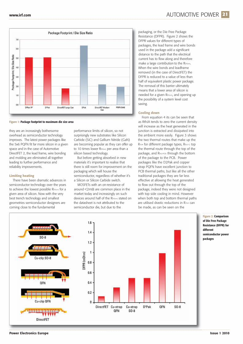
MOSFET greater the power density,however such a reduction in packagefootprint area must not be done at theexpense of RDS(on) or current carrying ability.Ultimately the designer wants to get thelowest RDS(on) possible in a given space. Asdie size and RDS(on) are inverselyproportional, calculating the ratio ofpackage footprint area to maximum diesize area for the given package is anindication of the RDS(on) performance that agiven package can offer in a given space.Figure 1 plots the ratio of package footprintto maximum die size area. In Figure 1, the ideal ratio would tend
towards 1, giving the least mm2 of PCBfootprint for a given RDS(on). However itclearly shows the area overhead that themore traditional packages such as theDPak and D2Pak place on the die sizearea, and ultimately the reduction incurrent density. The D2Pak has a packagefootprint to maximum die size area of 5;the package area is five times the size ofthe largest die size. Large Can DirectFEThowever offers a ratio of about 1.7 - soultimately on the PCB a given RDS(on) in asmaller space can be achieved.The technology and basic design of the
D2Pak and DPak have changed little overthe years, the leadframe, wrie bonds andmolding take up area and volume while atthe same time impeding performance;
Int Rec Feature_Layout 1 02/02/2010 10:10 Page 20
www.irf.com AUTOMOTIVE POWER 21
Power Electronics Europe Issue 1 2010
they are an increasingly bothersomeoverhead as semiconductor technologyimproves. The latest power packages likethe 5x6 PQFN fit far more silicon in a givenspace and in the case of AutomotiveDirectFET 2, the lead frame, wire bondingand molding are eliminated all togetherleading to further performance andreliability improvements.
Limiting heating There have been dramatic advances in
semiconductor technology over the yearsto achieve the lowest possible RDS(on) for agiven area of silicon. Now with the verybest trench technology and smallestgeometries semiconductor designers arecoming close to the fundamental
performance limits of silicon, so notsurprisingly new substrates like SiliconCarbide (SiC) and Gallium Nitride (GaN)are becoming popular as they can offer upto 10 times lower RDS(on) per area than asilicon based technology.
But before getting absorbed in newmaterials it’s important to realise thatthere is still room for improvement on thepackaging which will house thesemiconductor, regardless of whether it’sa Silicon or Silicon Carbide switch.
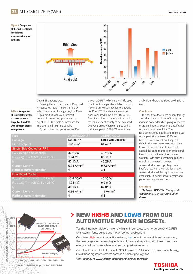
MOSFETs with an on-resistance ofaround <2m are common place in themarket today and increasingly on suchdevices around half of the RDS(on) stated onthe datasheet is not attributed to thesemiconductor die, but due to the
packaging, or the Die Free PackageResistance (DFPR). Figure 2 shows theDFPR values for different types ofpackages, the lead frame and wire bondsused in the package add a significantdistance to the path that the electricalcurrent has to flow along and thereforemake a large contribution to the RDS(on).When the wire bonds and leadframeremoved (in the case of DirectFET) theDFPR is reduced to a value of less thanhalf of equivalent plastic power package.The removal of this barrier ultimatelymeans that a lower area of silicon isneeded for a given RDS(on), and opening upthe possibility of a system level costsaving.
Cooling downFrom equation 4 its can be seen that
as RthJA tends to zero the current densitywill increase as the heat generated in thejunction is extracted and dissipated intothe ambient more easily. Figure 3 showsthe two thermal routes that make up theRthJA for different package types, Rth(J-C) topthe thermal route through the top of thepackage, and Rth(J-PCB) through the bottomof the package to the PCB. Powerpackages like the D2Pak and copperstrap PQFN have excellent junction toPCB thermal paths, but like all the othertraditional packages they are far lesseffective at allowing the heat generatedto flow out through the top of thepackage, indeed they were not designedwith top side cooling in mind. Howeverwhen both top and bottom thermal pathsare utilised drastic reductions in R thJA canbe made, as can be seen on the
Figure 1: Package footprint to maximum die size area
Figure 2: Comparisonof Die Free PackageResistance (DFPR) fordifferentsemiconductor powerpackages
Int Rec Feature_Layout 1 02/02/2010 10:10 Page 21
22 AUTOMOTIVE POWER www.irf.com
Issue 1 2010 Power Electronics Europe
DirectFET package type. Drawing the factors or space, RDS(on) and
RthJA together, Table 1 makes a side byside comparison of a large die, low RDS(on)
D2pak product with a counterpartAutomotive DirectFET product usingequation 4. The table summarises theimprovement in current density.
By taking two high performance 40V
power MOSFETs which are typically usedin automotive applications Table 1 showshow the simple construction of packagelike DirectFET, the elimination of wirebonds and leadframe allows RDS(on) PCBfootprint and RthJA to be minimised. Thisresults in current density to be increasedby over 3 times when compared with atraditional plastic D2Pak-7P, even in an
application where dual sided cooling is notused.
ConclusionThe ability to drive more current through
a smaller space, at higher efficiency andincrease power density is going to becomeof greater importance as the electrificationof the automobile unfolds. Thereplacement of fuel tanks and spark plugsof the past with batteries, IGBTs andMOSFETs of today will not happen bydefault. The new power electronic drivetrains will not only have to meet butexceed the performance of the traditionalinternal combustion engine poweredsolution. With such demanding goals theuse of next generation powersemiconductor power packages whichinterfere less with the operation of thesemiconductor will be key to ensure nextgeneration efficiency, power density andperformance goals are met.
Literature[1] Power MOSFETs, Theory and
Applications, Duncan Grant, JohnGower
Figure 3. Comparisonof thermal resistancesfor differentsemiconductor powerpackages
Table 1: Comparisonof Current Density fora D2Pak-7P and aLarge Can DirectFETwith different coolingarrangements
NEW HIGHS AND LOWS FROM OURAUTOMOTIVE POWER MOSFETs.Toshiba innovation delivers more new highs, in our latest automotive power MOSFETsfor motors in fans, pumps and motion control applications.
Combining high current capability with very low on resistance and thermal resistance, the new range also delivers higher levels of thermal dissipation, with three times more effective reduced source temperature than previous versions.
And at just 3.7mm thick, the latest MOSFETs are 21% thinner than previous technology.So all these big improvements come in a smaller package too.
Visit us today at www.toshiba-components.com/automosfet
250
200
150
100
50
00 20
DRAIN CURRENT, IC (A) @ 180 SECONDS
TO-220SM(W)
PREDECESSORS
APPROX. TWOFOLDCURRENT DRIVE
CAPABILITY
SO
UR
CE
LE
AD
TE
MP
. (@
18
0 S
EC
ON
DS
)
40 60 80 100 120 140 180
Int Rec Feature_Layout 1 02/02/2010 10:10 Page 22

“Tuesday and Wednesday wereboth very busy days with a goodcalibre of enquiries and a goodresponse. We had 12 peoplemanning the stand and theywere all very busy.”
Patrick O’Neill – WEG
“Initial indicators on the decisionto go back to Drives and Controlswere well founded. Quality leadsfrom a busy 3 days.”
Bradley McEwan – Rockwell Automation
“The Drives and Controlsexhibition has resulted on 40%increase enquiries taken over thethree days from the 2006exhibition.”
Tony Pickering – Danfoss
“Wow! As a first time exhibitorwe will certainly be back in2010.”
Mark Cooper – Wittenstein( formerly Alpha Gearheads)
“We are very pleased with theshow, it is one of the best showswe have ever exhibited at.”David Higham – Habasit Rossi
“Excellent visitor numbers eachday including blue chipcompanies.”
Nick Cadby – Ideas in Automation
“The show looked great and thesupport facilities were second tonone. The quantity and quality ofvisitor was excellent.”
John Attenborough –Marelli
“The leads we had surpassed ourexpectations and we need to talkabout booking a larger stand forthe 2010 event.”
Nigel Evenett – Lafert
“We think Drives and Controls isnow firmly established as the UK’snumber one exhibition forautomation and drives.”Dave Baston – Control Techniques
“Drives and Controls is the bestshow that we have exhibited at for8 years. We had more enquiries onthe first day than ever before.”
Carl Krajewski – HMK Technical Services
“Compared to 2006 we’ve seen anoticeable increase in visitors. Theco-location with the other showsmakes it a must see event forengineers.”
John Wilkins – Rittal Ltd
“A superb show. By the end of theTuesday we already knew that wewould be back in 2010.”
Dave Proud – KTR
www.drives2010.com
For further information and your FREE exhibition pack contact:Doug Devlin | T: 01922 644766 |M: 07803 624471 | E: [email protected] Langston | T: 01353 863383 |M: 07962 402454 | E: [email protected]
DFA Media Ltd | Cape House | 60a Priory Road | Tonbridge | Kent TN9 2BL | Tel: 01732 370340 | Fax: 01732 360034
The Drives and Controls Exhibition & Conference 20108-10 June 2010 NEC, Birmingham
Contact us now for your FREE exhibition pack and become part of the UK’s largest and mostsuccessful manufacturing event
Don’t miss out
2010BROCHUREAVAILABLE
NOW!
Testamonial_d&c_may08_Layout 1 02/02/2010 11:38 Page 1

Energy Harvesting Gets a Boost
24 ENERGY HARVESTING www.linear.com
Issue 1 2010 Power Electronics Europe
A wide range of low-power industrial sensors and controllers are turning to alternative sources of energy as theprimary or supplemental means of supplying power. Ideally, such harvested energy will eliminate the need forwired power or batteries altogether. Although energy harvesting has been emerging since early 2000 (itsembryonic phase), recent technology developments have pushed it to the point of commercial viability. Inshort, in 2010 we are poised for its “growth” phase. Building automation sensor applications utilising energyharvesting techniques have already been deployed in Europe, illustrating that the growth stage may havealready begun. Tony Armstrong, Director of Power Product Marketing, Linear Technology, USA
Transducers that create electricity fromreadily available physical sources such astemperature differentials (thermoelectricgenerators or thermopiles), mechanicalvibration (piezoelectric orelectromechanical devices) and light(photovoltaic devices) are becoming viablesources of power for many applications.Numerous wireless sensors, remotemonitors, and other low-powerapplications are on track to become near“zero” power devices using harvestedenergy only (commonly referred to as“nanoPower” by some).
Commercial acceptanceEven though the concept of energy
harvesting has been around for a numberof years, the implementation of a systemin a real world environment has beencumbersome, complex and costly.Nevertheless, examples of markets wherean energy harvesting approach has beenused include transportation infrastructure,wireless medical devices, tire pressuresensing, and of course, buildingautomation. In the case of buildingautomation, systems such as occupancysensors, thermostats and light switches caneliminate the power or control wiringnormally required and use a mechanical orenergy harvesting system instead.
Similarly, a wireless network utilising anenergy harvesting technique can link anynumber of sensors together in a buildingto reduce heating, ventilation & airconditioning (HVAC) and lighting costs byturning off power to non-essential areaswhen the building has no occupants.Furthermore, the cost of energy harvestingelectronics is often less than running sensewires, so there is clearly economic gain tobe had by adopting a harvested powertechnique.
A typical energy scavenging
configuration or system, (represented bythe four main circuit system blocks shownin Figure 1/2), usually consists of a freeenergy source such as a thermoelectricgenerator (TEG) or thermopile attached toa heat generating source, such as anHVAC duct for instance. These smallthermoelectric devices can convert smalltemperature differences into electricalenergy. This electrical energy can then beconverted by an energy harvesting circuit(the second block in Figure 2) andmodified into a usable form to powerdownstream circuits. These downstreamelectronics will usually consist of somekind of sensor, analogue-to-digitalconverter and an ultra-low powermicrocontroller (the third block in Figure2). These components can take thisharvested energy, now in the form of anelectric current, and wake up a sensor totake a reading or a measurement thenmake this data available for transmissionvia an ultra-low power wireless transceiver- represented by the fourth block in thecircuit chain shown in Figure 2.
Each circuit system block in this chain,with the possible exception of the energysource itself has had its own unique set ofconstraints that have impaired itscommercial viability until now. Low cost
and low power sensors andmicrocontrollers have been available forquite sometime; however, it is only withinthe last couple of years that ultra-lowpower transceivers have becomecommercially available. Nevertheless, thelaggard in this chain has been the energyharvester and power manager.
Existing implementations of the powermanager block are a low performancediscrete configuration, usually consisting of35 components or more. Such designshave low conversion efficiency and highquiescent currents. Both of thesedeficiencies result in performancecompromised in an end system. The lowconversion efficiency will increase theamount of time required to power up asystem, which in turn increases the timeinterval between taking a sensor readingand transmitting this data. A high quiescentcurrent limits how low the energy-harvesting source can be since it must firstovercome the current level needed foroperation before it can use any excess tosupply power to the outputs.
New boost converter and systemmanager
What has been missing until now hasbeen a highly integrated DC/DC boost
Figure 1: The LTC3108 serves as ultra-lowvoltage boost converter and power manager in
energy-scavenging systems
Linear Feature_Layout 1 02/02/2010 10:15 Page 24

www.linear.com ENERGY HARVESTING 25
Power Electronics Europe Issue 1 2010
converter that can harvest and managesurplus energy from extremely low inputvoltage sources. However, the LTC3108(Figure 1), an ultra-low voltage boostconverter and power manager, greatlysimplifies the task of harvesting andmanaging surplus energy from extremelylow input voltage sources such asthermopiles, thermoelectric generators(TEGs) and even small solar panels. Itsstep-up topology operates from inputvoltages as low as 20mV. This is significantsince it allows the LTC3108 to harvestenergy from a TEG with as little as 1Ktemperature change.The circuit shown in Figure 3 uses a
small step-up transformer to boost theinput voltage source to a LTC3108 whichthen provides a complete powermanagement solution for wireless sensingand data acquisition. It can harvest smalltemperature differences and generate
system power instead of using traditionalbattery power. The LTC3108 utilises a depletion mode
N-channel MOSFET switch to form aresonant step-up oscillator using anexternal step-up transformer and a smallcoupling capacitor. This allows it to boostinput voltages as low as 20mV highenough to provide multiple regulatedoutput voltages for powering other circuits.The frequency of oscillation is determinedby the inductance of the transformer’ssecondary winding and is typically in therange of 20kHz to 200kHz.For input voltages as low as 20mV, a
primary-secondary turns ratio of about1:100 is recommended. For higher inputvoltages, a lower turns ratio can be used.These transformers are standard, off-the-shelf components, and are readily availablefrom magnetic suppliers. Our compounddepletion mode N-channel MOSFET is
what makes 20mV operation possible. The LTC3108 takes a “systems level”
approach to solving a complex problem. Itcan convert the low voltage source andmanage the energy between multipleoutputs. The AC voltage produced on thesecondary winding of the transformer isboosted and rectified using an externalcharge pump capacitor and the rectifiersinternal to the LTC3108. This rectifier circuitfeeds current into the VAUX pin, providingcharge to the external VAUX capacitor andthen the other outputs.The internal 2.2V LDO can support a
low-power processor or other low powerICs. The LDO is powered by the highervalue of either VAUX or VOUT. This enables itto become active as soon as VAUX hascharged to 2.3V, while the VOUT storagecapacitor is still charging. In the event of astep load on the LDO output, current cancome from the main VOUT capacitor if VAUX
drops below VOUT. The LDO output cansupply up to 3mA.The main output voltage on VOUT is
charged from the VAUX supply and is userprogrammable to one of four regulatedvoltages using the voltage select pins VS1and VS2. The four fixed output voltage are:2.35V for supercapacitors, 3.3V forstandard capacitors, 4.1V for Lithium-Ion
Figure 2: The four main blocks of a typical energy-scavenging system
www.paktron.com
Applications
MissionCritical
www.paktron.com
Linear Feature_Layout 1 02/02/2010 10:15 Page 25

26 ENERGY HARVESTING www.linear.com
Issue 1 2010 Power Electronics Europe
battery termination or 5V for higher energystorage and a main system rail to power awireless transmitter or sensors therebyeliminating the need for multi-M externalresistors. As a result, the LTC3108 does notrequire special board coatings to minimiseleakage, such as discrete designs wherevery large value resistors are required. A second output, VOUT2, can be turned on
and off by the host microprocessor usingthe VOUT2_EN pin. When enabled, VOUT2 isconnected to Vout through a P-channelMOSFET switch. This output can be usedto power external circuits such as sensorsor amplifiers that do not have low power
Figure 3: The LTC3108 used in a wireless remotesensor application powered from a TEG (Peltier cell)
sleep or shutdown capability. An exampleof this would be to power on and off aMOSFET as part of a sensing circuit withina building thermostat.The VSTORE capacitor may be a very large
value (even multiple Farads), to providehold-up at times when the input powermay be lost. Once power-up has beencompleted, the main, backup and switchedoutputs are all available. If the input powerfails, operation can still continue, operatingoff the VSTORE capacitor. The VSTORE output canbe used to charge a large storage capacitoror rechargeable battery after VOUT hasreached regulation. Once VOUT has reached
regulation, the VSTORE output will be allowedto charge up to the VAUX voltage, which isclamped at 5.3V. Not only can the storageelement on VSTORE be used to power thesystem if the input source is lost but it canalso be used to supplement the currentdemanded by VOUT, VOUT2 and the LDOoutputs if the input source has insufficientenergy.
ConclusionWith analogue switchmode power
supply design expertise in short supplyaround the globe, it has been difficult todesign an effective energy harvestingsystem as illustrated in Figure 1. However,with the introduction of the LTC3108thermal energy harvesting, DC/DC boostconverter and system manager that’s allabout to change. This device can extractsenergy from solar cells, thermo-electricgenerators or other similar thermalsources. Furthermore, with iscomprehensive feature set and ease ofdesign, it greatly simplifies the hard-to-dopower conversion design aspects of anenergy harvesting chain.
IXYS 600V GenX3SCTM
THE B 600V SIXYYS
JUST ESCSenX3G TM
BT GOT S
ERTT BE
Linear Feature_Layout 1 02/02/2010 10:15 Page 26

Natural match!
Features+15V/-10V gate voltage3W output power20A gate current80ns delay timeDirect and half-bridge modeParallel operationIntegrated DC/DC converterElectrical isolation for 1700V IGBTsPower supply monitoringShort-circuit protectionFast failure feedbackSuperior EMC
2SP0320 is the ultimate driver platform for PrimePACKTM IGBT modules. As a member of the CONCEPT Plug-and-play driver family, it satisfies the requirements for optimized electrical performance and noise immunity. Shortest design cycles are achieved without compromising overall system efficiency in any way. Specifically adapted drivers are available for all module types. A direct paralleling option allows integrated inverter design covering all power ratings. Finally, the highly integrated SCALE-2 chipset reduces the component count by 80% compared to conventional solutions, thus signifi-cantly increasing reliability and reducing cost. The drivers are available with electrical and fiberoptic interfaces.
PrimePACKTM is a trademark of Infineon Technologies AG, Munich
2SP0320
SAMPLES AVAILABLE!
CT-Concept Technologie AG, Renferstrasse 15, CH-2504 Biel, Switzerland, Phone +41-32-344 47 47 www.IGBT-Driver.com
27_PEE_0110_27_PEE_0110 02/02/2010 11:40 Page 1

Design Concept for aTransformerless Solar Inverter
28 RENEWABLE POWER www.vincotech.com
Issue 1 2010 Power Electronics Europe
Vincotech is able to offer a wide spectrum of power modules for solar applications. For transformer-lesssingle phase solar inverter the power module FZ06BIA045FH-P897E is able to carry a output power of 6kWbut for efficiency optimisation a nominal power of 3kW is recommended. Michael Frisch and TemesiErnö, Vincotech Germany and Hungary
The topology is supporting the requiredfunctions of adjustment to the maximumpower point (MPP) of the solar string andinverting to sinusoidal output current andvoltage (see Figure 1).
BoosterThe booster is active when the solar
voltage is below the peak of the powergrid voltage.In this case the booster (T5, D8,9) sets
the MPP for the photo voltaic solar cell(PV). When the PV MPP voltage reachesthe peak of the line, the bypass diode(D7) cuts boost stage losses. Theadjustment of the MPP has to becontrolled by the output H-bridge inverter.The output of the booster is the DC linkvoltage, filtered by a capacitor (C4). Thiscapacitor should be a parallel compositionof a high tangent delta film capacitor andan electrolytic capacitor. The highfrequency capacitor have to be placed
Figure 1: Single phase,transformer-lessinverter topology
Figure 2: Dual inductorwith split winding
Vinotech Feature_Layout 1 02/02/2010 10:29 Page 28
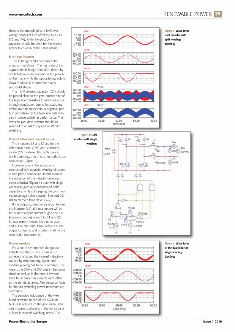
www.vincotech.com RENEWABLE POWER 29
Power Electronics Europe Issue 1 2010
close to the module pins to limit over-voltage shoots at turn off of the MOSFET(T2 and T4), while the electrolyticcapacitor should be sized for the 100Hzpower fluctuation of the 50Hz mains.
H-bridge inverterThe H-bridge works by asymmetric
unipolar modulation. The high side of theasymmetric H-bridge should be driven by50Hz half-wave dependent on the polarityof the mains while the opposite low side isPWM modulated to form the mainssinusoidal shape.The 10nF ceramic capacitor (C5) should
be placed close to the gate-emitter pins ofthe high side transistors to eliminate crossthrough conduction due to fast switchingof the low side transistors. A negative gateturn off voltage on the high side gate mayalso improve switching performance. Thelow side gate drive resistor should beselected to adjust the speed of MOSFETswitching.
Output filter and current senseThe inductors L1 and L2 are for the
differential mode (DM) and commonmode (CM) voltage filter. Both have adouble winding, one of each in both phaseconnection (Figure 2). However one of the inductors is
connected with opposite winding directionin one phase connection. In this mannerthe utilisation of the inductor becomesmore effective (Figure 3) than with singlewinding (Figure 4) inductors and deltacapacitors, while still keeping the commonmode voltage noise between line and DClink to an even lower level (Vcmd). If the output current sense is put before
the inductor (L1), the test current will bethe sum of output current to grid and CM(common mode) current to C1 and C2.So two current senses have to be usedand put on the output line before L1. Theoutput current to grid is determined by thesum of the two currents.
Power module For a conclusive module design low
induction in the DC-link is a must. Toachieve this target, the internal inductivitycaused by wire bonding, layout andmodule pinning has to be minimised. Thismeans the DC+ and DC- pins in the boostcircuit as well as in the output inverterhave to be placed as close to each otheras the standards allow. Also sense contactsfor the fast-switching power transistors arenecessary. The parasitic inductance of the wire
bond at switch on/off of the IGBTs orMOSFETs will reduce the gate signal. Thismight cause oscillations in the transistor orat least increased switching losses. The
Figure 3: Wave formdual inductor withsplit windingstopology
Figure 5: Wave formof the dual inductorsingle windingtopology
Figure 4: Dualinductors with single
windings
Vinotech Feature_Layout 1 02/02/2010 10:29 Page 29

30 RENEWABLE POWER www.vincotech.com
Issue 1 2010 Power Electronics Europe
current-less sense wire, bonded directly onthe source or emitter pad of the transistorchip, will eliminate the problem. This isonly possible with module technology.Figure 6 shows the Vincotech standard
module flowSOL0-BI (P896-E01) whichincorporates the functions listed previouslysuch as:• Boost circuit with MOSFET(600V/45m) and SiC rectifier• Bypass diode for maximum power(when exceeding nominal power)• H-bridge with 50A/600V IGBTs andSiC rectifier in the high side andMOSFET (600V/45m) in the lowside* Temperature Sensor
EfficiencyA simulation based on measured values
of this circuit (here are only thesemiconductor losses considered) showsthe following results (conditions PIN = 2kW,fPWM = 16kHz, VPVnominal = 300V, VDC = 400V):The efficiency for the module (booster +inverter) is 98,8%. This shows that a totalefficiency, including the passivecomponents, of 98% is reachable. Figure7 also shows that the efficiency of thealternative full IGBT solution dropssignificantly at partial load.
ABOVE Figure 6: ModuleflowSOL0-BI incorporatingboost circuit and mixedinverter
RIGHT Figure 7: Efficiencysimulation result for the
output inverter shows 99,2%compared to 97,2% of a pure
IGBT solution (dotted line)
To receive your own copy of
subscribe today at:
www.power-mag.com
To receive your own copy of
subscribe today at:
www.power-mag.com
Vinotech Feature_Layout 1 02/02/2010 11:06 Page 30

www.lem.com BATTERY MONITORING 31
Power Electronics Europe Issue 1 2010
Monitoring Batteries ImprovesUPS ReliabilitySystems from mobile telecommunications to data centres must operate with minimal downtime, makingthe reliability of the electrical mains supply a key concern. Uninterruptable power supplies (UPSs), whichprovide back-up power in the event of mains failure, are therefore widely used to ensure critical electronicsystems continue to function normally in the event that the mains power goes down. Sentinel III; a set ofcomponents for a battery monitoring addresses the needs of UPS OEMs and battery providers. Thesecomponents are used to create a simple to install and intuitive solution for continuous battery monitoringwithin mission critical installations. Loic Moreau, LEM SA, Geneva, Switzerland
Although other technologies, such asflywheels, can be used, most UPSs usebatteries to store energy. Batteries providesignificant capacity and are able to deliverpower almost instantaneously. If the UPS isto operate reliably, it is essential that thebatteries are not only fully charged, butalso in good condition.
High influence on UPS performanceBattery cells have a limited lifetime,
which can be shortened considerably if theenvironmental conditions - particularlytemperature - are outside the optimumrange. In most installations cells arereplaced at a fixed interval based upon thewarranty - typically every five years. Thisapproach is imperfect: batteries operatedoutside of the expected environmentalconditions can fail sooner, whilst wellmaintained batteries might have a longerlifetime.Modern UPSs are required to deliver
high power levels, and therefore manycells are required. In large strings, a failurein a single cell can cause the whole stringto fail. Large and medium UPSs willimplement redundancy to ensure that astring failing does not result in the entireUPS failing. Whilst the UPS will continue tooperate, the peak current that can bedelivered and the time for which thesystem can run using the UPS will both bereduced. Furthermore a failed cell candamage the other blocks in the string,reducing their lifetime.Battery monitoring and maintenance
represents a significant cost associatedwith running UPSs. Typically an engineervisits the site on a regular basis - perhapsmonthly - to measure the electricalcharacteristics of the cells in the system.Typically the voltage of the cell will bemeasured, identify cells operating out ofrange, which will then be replaced. Outputvoltage is not always a good predictor of
Figure 1: Battery cell output voltage
Figure 2: Cell failure
LEM_Feature_Layout 1 02/02/2010 10:57 Page 31

32 BATTERY MONITORING www.lem.com
Issue 1 2010 Power Electronics Europe
failure, so cells may fail in between theseregular visits, require an additional service.
Permanent monitoring of batteries notonly reduces cost by reducing the time foran engineer to physically check the state ofeach of the batteries, making their sitevisits more efficient, but also allows forpreventative maintenance. By identifyingpotential failures, cells can be swapped outduring routine visits, ensuring greaterreliability and removing the need foremergency engineer visits.
Monitoring a large UPSLEM used the Sentinel (see Sidebar)
battery monitoring system to measure thecells in a broadcast facility with an 800kVAUPS. Figure 1 shows the output voltages ofa number of cells in one of the strings. Inthis case each string had 200 monoblocks,delivering around 440V. There isconsiderable variation in the voltage, whichis due to incorrect configuration of thebattery conditioning, which is discussedlater in this article.
The graph clearly shows one cell isdelivering 2V, rather than the nominal 2.2V.Although the block is producing a lowervoltage than expected, the difference isrelatively small, and is stable. Thisbehaviour is typical, making the use ofoutput voltage as an indicator of impedingfailure is unreliable, as the voltages can beremain within thresholds and thereforealarms are not triggered.
In this case, the battery monitoringsystem was being used to assess theeffectiveness of the scheduledmaintenance approach, and not to warn ofpotential problems. As no action wastaken, Figure 2 shows that on 9th October(10/9) the cell fails catastrophically. Notethat prior to the cell voltage dropping to0.7V, the voltage of the faulty blockremains constant, giving no indication thatthe block is about to fail. The voltagereturns to normal on 19th Novemberwhen the cell was replaced.
The output voltage is not a goodpredictor of likely failure, as there was nochange in its value prior to the failure ofthe cell. Another characteristic of the cell -impedance - is a much better indicator asFigure 3 shows. This graph illustrates theimpedance rising in June, and by the startof July the value has increased by morethan 20%. A trend is easy to detect:measuring impedance could haveidentified the problem three monthsbefore the cell failed. If the customer usedthe impedance data, the cell could havebeen replaced during regular preventativemaintenance before its deteriorationcaused the failure.
Permanent monitoring provides otheruseful information that can help increase
UPS reliability. For the example in Figure 1it is clear that there are plenty ofcharge/discharge cycles (shown by thespikes on the voltage trace). Although allbatteries need to undergo conditioning thebattery discharge is much too frequent,with 4-5 discharges per month. Whilstsome battery conditioning lengthens life,too many discharge cycles will reduce thelifetime: a normal configuration will cycleonly two or three times per year. Typicallycells have a guaranteed lifetime of 20-50cycles. In the case we are considering thebatteries would have exceeded this in justa few months, and a strategy of replacingbatteries every five years would mean thatthe cells would undergo several timesmore discharge cycles than they weredesigned to endure.
The frequent charge/discharge cycles atthis site were caused by the installerleaving the UPS in a commissioning modethat cycles the battery charge frequently toallow testing - a surprisingly commonmistake that can drastically shorten thelifetime of the batteries. Erroneousconfigurations will not be obvious toengineers during their visits to the site -continuous automatic monitoring, however,makes the problem obvious.
Another cause of shortened batterylifetime is high temperature. Even a smallincrease in temperature increases the rateof the unwanted chemical reactions in thebattery that ultimately cause it to fail.Typically battery manufacturers quotelifetimes at 20°C. Figure 4 shows theambient temperature in this system varying
Figure 3: Cell impedance predicts failure
Figure 4: Temperature monitoring
LEM_Feature_Layout 1 02/02/2010 10:57 Page 32

www.lem.com BATTERY MONITORING 33
Power Electronics Europe Issue 1 2010
with time, and at one point reaching22°C. The air conditioning failed tomaintain the temperature within anacceptable range, which will result ina reduction in battery life.Furthermore the increasedtemperature may void the batterymanufacturer’s warranty.
ConclusionPermanent battery monitoring
offers many advantages, beyond thereduction in cost by making site visitsby engineers more efficient. In thisexample automatic monitoring of theimpedance of the battery would haveidentified a failing cell three monthsbefore the cell became faulty.Continuous monitoring also makesidentifying UPS configuration
problems simple: particularly incorrectcharge/discharge frequency that candramatically reduce battery life.Monitoring measures ambientconditions, ensuring that lifetime isnot reduced because of hightemperatures. Monitoring maximisesthe life of the cells, reducing the riskof failure and saving money byensuring that strings do not need tobe replaced prematurely, as well asensuring early detection ofdeteriorating cells, often allowingreplacement before the string goesdown. Although critical systems suchas UPSs are usually not the first targetfor cost savings, it is important thatusers switch to permanent monitoringas it both cuts cost and increasesreliability.
The Sentinel solution comprisestransducers, data loggers andsoftware components to create astandby battery monitoring solution(SBM). In order to extend thefunctionality of the existing Sentinel,LEM has developed the S-Box; adata logger featuring an embeddedwebserver, which enablesadministrators to monitorinstallations remotely. The state-of-the art measurement and datalogging features include bloc, stringand battery voltage measurement,Bloc temperature and impedancemeasurement, discharge
performance and discharge/chargecurrent. The S-Box also measuresambient temperature, a key factoraffecting battery life.The Sentinel transducer is
designed to reduce installation time,offering DIN-rail mounting and anexternal temperature patch. Userscan set up an alarm for each of theparameters measured by thetransducers connected to the S-Box.As well as instant alarms the S-Boxcan also provide a weekly report tothe administrator, containing all dailymeasurements and critical systeminformation.
Sentinel III BatteryMonitoringComponents
Components of Sentinel III battery monitoring system
MAKING MODERN LIVING POSSIBLE
DANFOSS SILICON POWER
SILICONPOWER.DANFOSS.COM
The coolest approach to heat transferBenefit from the most cost-efficient power modules available
It cannot be stressed enough: Efficient cooling is the most important feature in regards to Power Modules. Danfoss Silicon Power’s cutting-edge ShowerPower® solution is designed to secure an even cooling across base plates, offering extended lifetime at no increase in cost. All our modules are customized to meet the exact requirements of the application. In short, when you choose Danfoss Silicon Power as your supplier you choose a thoroughly tested solution with unsurpassed power density.
Please go to siliconpower.danfoss.com to learn about Power Modules that are second to none.
ShowerPower®
LEM_Feature_Layout 1 02/02/2010 11:02 Page 33

34 POWER MODULES www.mitsubishielectric.de
Issue 1 2010 Power Electronics Europe
Thermal Behaviour of Three-Level Trench Gate IGBT Modulesin PFC and PV OperationThe control of the power semiconductors in a three-level NPC topology employs a set of 12 control signalsin total. A back-to-back two-level/three-level inverter has been built to circulate power performing arbitraryload conditions to analyse the thermal dissipation of the power semiconductors. This thermal analysisutilises an IR camera to perform an in-situ measurement and allows precise modelling of thermal andelectrical parameters. Once this experimental platform has been calibrated, the loss on each semiconductorchip can be acquired and compared with the simulated results. Hence, tuning of the model parametersbecomes possible. Marco Honsberg and Thomas Radke, Mitsubishi Electric Europe, Germany
The continuously growing consciousnesstowards energy saving needs have led tointense research towards highly efficientpower conversion methods. OnlineUninterruptible Power Supplies (UPS)being connected and loaded 24 hours and7 days, as well as photovoltaic (PV)inverters, are dedicated applications with ahigh potential in energy saving by anincrease of the total system’s efficiency.Besides the continuous improvement ofthe power device’s inherent lossperformance and the outlook to haveSilicon Carbide (SiC) based switchingdevices and their optimised packagingtechnology widely available in a few years,three-level technology has been foundefficient in decreasing a system’s powerloss.Three-level IGBT modules, with their
comparatively complex structure in terms ofchip layout and their thermal performanceunder varying load conditions, are essentialto fabricate a compact and reliable three-level inverter. Figure 1 shows a view into anopened three-level 13in one IGBT module.In addition to the pure NPC three-levelstructure, there is a 1200V-class IGBT toperform a braking operation in conjunctionwith the employed free-wheeling diode(FWD). Such a braking operation canbecome necessary in case a regenerativeload is connected to the UPS. The circuitryof the module is shown in Figure 2.All chips forming a P-side and,
respectively, an N-side functional group, e.gT 1, T 2 and their FWDs and Clamp diodes(CLDs) and T 3, T 4, their FWDs and theCLDs, respectively, for the N-side arelocated on one AlN ceramic substrate for Figure 2: Three-level IGBT module topology including circuitry
Figure 1: Openedthree-level IGBTmodule
Feature Mitsubishi_Layout 1 02/02/2010 11:21 Page 34
www.mitsubishielectric.de POWER MODULES 35
Power Electronics Europe Issue 1 2010
best thermal conduction. The internallayout, power chips and the thermal profilein a sample module has been analysed bythermograph and baseplate temperaturesensors under varying load.
Three-level NPC topology and shortcircuit detectionThe outer switches (IGBT 1 and IGBT 4)
are equipped with a real-time currentcontroller (RTC), a unique technologyutilising a fraction of the collector current todetect an over-current situation and to forcethe IGBT into a current controlleddesaturation. The principle of the RTC and itslocation on the substrate is shown in Figure3. Basically, the aforementioned fraction ofthe collector current is flowing through theshunt resistor (inside the red dashed line ofFigure 3) and creates a voltage dropaccordingly. The following comparator pullsdown the Gate Emitter voltage (Vge) whenthe reference voltage level (Vref) is exceededby shunt voltage drop. A similar circuit has been used in
previous generations of Intelligent PowerModules (IPM) for more than 10 years tocontrol the desaturation current levelprecisely, and has been adopted here foran IGBT module the first time. As a result,the comparatively low current level reducesthe stress on the IGBT during a short-circuitsituation. Such a stress reduction improvesthe reliability of key applications like PVinverter and UPS. The increase of MTBF isa key objective for UPS applications wherepower quality and availability, as well as along lifetime, is a main target for PVinverter. The inner IGBTs (2 and 3) arelacking this RTC, leading to a higherdesaturation current. Hence, the moduleprovides an essential feature to efficientlyprotect a three-level inverter system inshort-circuit situations, as the describeddeliberate implementation of RTCs at IGBT1 and IGBT 4 ensure that inner IGBTs(IGBT 2 and IGBT 3) would neverdesaturate before the outer ones. Thisfeature of the three-level IGBT modules is
simplifying the gate driver and theconnected fault detection logic usuallybeing implemented into a programmablelogic device.
Power loss calculation approachThe thermal evaluation has been done
by the modelling of the device and thecharacterisation of loss parameters likeswitching and conduction losses as afunction of their influencing parameter.With this device data and the knowledgeabout the commutation in a real inverteroperation, it becomes possible to performa loss simulation for the specific operationconditions which are considered typical forPV-inverter or UPS operation. In three-level NPC configuration, the
number of commutation paths issubstantially higher and leads to a morecomplex way of calculating loss for theindividual FWD/CLD or IGBT chip. Thevalue and the direction of the current, inconjunction with the output voltagerepresented by a pulse width modulated(PWM) signal and their phase angle inbetween, are the input parameters of theloss calculation approach. Additionally, thechip inherent loss dependencies: • Vce(sat) = f(Ic, Tj), • VF = f(IE, Tj), • Eon, Eoff, Err = f(Ic, RG, Vcc, Tj)have to be taken into account, where
Vce(sat) is the saturation voltage, Ic is thecollector current, Tj is the junctiontemperature of the chip and Eon, Eoff are theswitching energies to turn on or off thedevice and Err to recover the incorporateddiodes respectively.RG represents the connected gate
resistance and Vcc is the DC-link voltage. Anarbitrary combination of voltage and currentand their phase angle between themneeds to be considered when performingthe loss calculation (Figure 4). In theexample during the interval where currentand output voltage are having equalpolarity, the ‘outer’ IGBT (IGBT 1 or IGBT 4respectively) together with theircorresponding clamp diodes are switching/recovering while the inner IGBTs (IGBT 2and IGBT 3 respectively) are only havingconduction losses as a function of the
Figure 3: RTCoperation and chip
Figure 4: Arbitrarycombination ofvoltage and current
Figure 5: Black painted chips
Feature Mitsubishi_Layout 1 02/02/2010 11:21 Page 35

36 POWER MODULES www.mitsubishielectric.de
Issue 1 2010 Power Electronics Europe
actual output current polarity. In the sameway, the active components and theirindividually imposed loss must beidentified in the remaining intervals toperform a calculation over one cycle andhence getting an image of the total lossinside the module.In reality, the voltage waveform is usually
established by a PWM signal, which isadjusting the (fixed) DC-link voltage to themean output voltage value of the switchinginstance by the applied duty cycle ‘D’. If thethermal simulation is done in this preciseway, pulse by pulse, the calculation of totalloss becomes simple by summarising theloss per switching instant or pulse ‘p’.With t1=φ and t2=π , this specific
calculation for T1 can be performedaccording to equations 1 - 5 considering PSSsteady state or conduction loss and PSWswitching loss.
1)
2)
3)
4)
5)
Loss calculation in PV-inverter and UPSespecially for the front end portion of theUPS (3~ PFC) are quite simple because ofa simplification of the interval situation.Assuming sinusoidal shape of currentwaveforms, the calculation can beperformed according to the aforementionedequations. The correctness and theprecision of such a loss calculation ischecked to allow a tuning of parameters toreach a good matching between simulationand reality. Hence, a precise measurement
instead of simulation of loss under realisticconditions provides the required precisionfor a simulation tool. For this purpose, aback-to-back configuration of inverters hasbeen developed that is able to perform acirculation of power. Hence, the specificconditions found in PV-inverter operationand 3~ PFC operation can be createdeasily, helping to investigate on the thermalbehaviour and evaluate the performance oftwo- and three-level IGBT modules.
Load generation test set-upBefore applying the realistic application
conditions the setup consisting of the IGBTmodule and the heatsink was prepared andcalibrated. For this purpose the deviceunder test (DUT), a 75A three-level IGBTmodule CM75YE13-12F, has beenequipped with various thermocouplesmounted into the baseplate just under the
specific IGBT or diode chip. Moreover, thegel has been removed from the moduleand the bare chips have been coated by ablack varnish with known emissioncoefficient. Figure 5 shows the result afterthe coating.In order to acquire the thermal
resistance from junction to the baseplatefor each chip precisely a DC current testhas been performed, which is powering allavailable IGBTs by one current source andthe DUT by a separate current source tocreate realistic temperature gradients in themodule’s baseplate. As a result of thechosen set-up, two entire legs are poweredby one current source and the positive/negative part of the leg where the DUT islocated is powered separately. At the DUT,along with the precise DC currentmeasurement, a Vce(sat) measurement isperformed on chip level (Figure 6).
Figure 6: Test set-upto determine thethermal resistance ofthe DUT
Figure 7: Thermal investigation by a set of two inverters which are circulating the power
Feature Mitsubishi_Layout 1 02/02/2010 11:21 Page 36

www.mitsubishielectric.de POWER MODULES 37
Power Electronics Europe Issue 1 2010
The thermocouple touching thebaseplate just under the chip and theinfrared camera is observing the blackpainted surface of the IGBT/FwDi chip. TheDC-loss of this selected operation point iswell-known and the thermal resistance canbe determined by linking power loss andtemperature rise by means of the thermalresistance, according to the well knownequation 6:
6)
The thermal investigation has beenperformed by a set of two inverters whichare circulating the power. Figure 7 revealsthe configuration of the experimental test-bench which allows the setting up ofarbitrary operation conditions for the powerstage by a digital control of DC-link voltage,switching frequency load currents, PFC/inverter mode and current phase angle.Hence, the loss distribution inside the IGBTmodule can be shifted and thecorresponding individual chip temperatureobserved accordingly.
Application conditions for PV-invertersIR images of typical operation conditions
for PV- inverter, e.g. cos(φ) =1 andmodulation index variation of 0.5 to 1.0,PFC operation and also mixed conditionswith highly capacitive or inductive loadhave been tested. The case presentedbelow shows the typical operation underPV conditions operating at the followingapplication parameters:• Vcc = 750V• Î = 50A• modulation ratio = 69%• cos(φ) = 1• fc = 10kHz• fo = 50Hz• Tf = 65°C
By the interpretation of the thermal imageand considering the corresponding baseplatetemperature of the chip, the power loss canbe calculated according to equation 6.
From the IR image (Figure 8), theabsolute temperatures can be easily readout and it becomes clear that in thisoperation, as already described in thepower loss calculation approach, thermallythe outer IGBT T1 is the bottleneck. TheFWDs are not taking over any load as
theoretically already understood. Hence,the colour of the IR image indicates asubstrate temperature accordingly. It isremarkable that, in this operation, theclamp diode (clamp) is thermally onlyslightly loaded despite the smallmodulation index of only 0.69. Withrespect to PV-applications, it is an indicationof a conservatively selected chip size insidethis three-level IGBT module.
Furthermore, a qualitative result on thejunction temperature change as a functionof varying phase angle between currentand voltage explains that the set-up of chipsizes inside a module can be optimised forcertain operation conditions. The shift ofload reflected in the thermal dissipation asa function of the cos(φ) is indicated in theIR images shown in Figure 9. For all ofthese tests, the amplitude of the currentand the modulation index have been keptconstant, but they are different comparedwith the previously measurement results.Referencing to the naming convention,according to Figure 2, all measurementshave been taken out of leg V and D1 is theFWD to T1 and Dc1 is the CLD of thepositive part of the leg.
From these images, it can be understood
that the lower the cos(φ) is the lower thepower loss in T1 gets. T2 shows a quitestable dissipation under all these changingconditions. However, the origin of this powerloss is changing: While in the case of cos(φ)= 1 T2 is mainly heated by conduction loss,the situation at PFC operation (cos(φ) = -1)is changed to a mixture of (less) conductionloss but more switching loss.
The differences indicated as ERRORbetween real measurement and simulatedresults are very small. The results presentedin Table 1 show a good match.
ConclusionThe inverter and the control structure
according to Figure 2 has been calibratedand successfully commissioned to generaterealistic test conditions for the optimisation oftwo- and three-level IGBT modules. IRimages and the analysis of the correspondingloss information has led to the conclusionsregarding the suitability of the chip set-up ofthe suggested three-level IGBT moduleunder PFC and PV-inverter operation withvarying power factor. The results show thepotential hotspots inside a three-level IGBTmodule depending on the actual loadconditions and allow for optimising a losssimulation tool.
Literature‘Three-level Trench Gate IGBT
modules with IGBT and their thermalanalysis in UPS, PFC and PV operationmodes’, published at EPE 2009 -European Conference on PowerElectronics and Applications, Barcelona,8-10 September 2009
Figure 9: Chip temperatures at cos(φ) variation
Figure 8: IR imageindicating theabsolute chiptemperatures
Table 1: Temperaturerise ΔT(j-c) resultscalculated versusmeasured results
Feature Mitsubishi_Layout 1 02/02/2010 11:21 Page 37
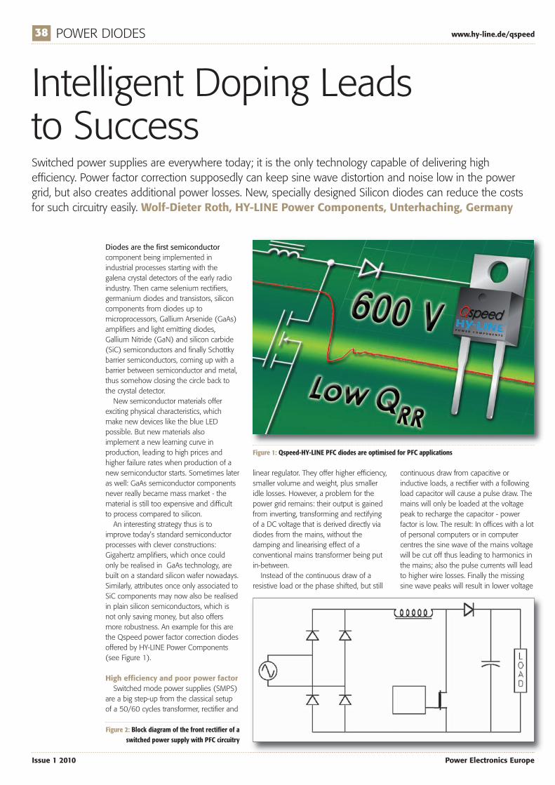
Intelligent Doping Leads to Success
38 POWER DIODES www.hy-line.de/qspeed
Issue 1 2010 Power Electronics Europe
Switched power supplies are everywhere today; it is the only technology capable of delivering highefficiency. Power factor correction supposedly can keep sine wave distortion and noise low in the powergrid, but also creates additional power losses. New, specially designed Silicon diodes can reduce the costsfor such circuitry easily. Wolf-Dieter Roth, HY-LINE Power Components, Unterhaching, Germany
Diodes are the first semiconductorcomponent being implemented inindustrial processes starting with thegalena crystal detectors of the early radioindustry. Then came selenium rectifiers,germanium diodes and transistors, siliconcomponents from diodes up tomicroprocessors, Gallium Arsenide (GaAs)amplifiers and light emitting diodes,Gallium Nitride (GaN) and silicon carbide(SiC) semiconductors and finally Schottkybarrier semiconductors, coming up with abarrier between semiconductor and metal,thus somehow closing the circle back tothe crystal detector.New semiconductor materials offer
exciting physical characteristics, whichmake new devices like the blue LEDpossible. But new materials alsoimplement a new learning curve inproduction, leading to high prices andhigher failure rates when production of anew semiconductor starts. Sometimes lateras well: GaAs semiconductor componentsnever really became mass market - thematerial is still too expensive and difficultto process compared to silicon.An interesting strategy thus is to
improve today’s standard semiconductorprocesses with clever constructions:Gigahertz amplifiers, which once couldonly be realised in GaAs technology, arebuilt on a standard silicon wafer nowadays.Similarly, attributes once only associated toSiC components may now also be realisedin plain silicon semiconductors, which isnot only saving money, but also offersmore robustness. An example for this arethe Qspeed power factor correction diodesoffered by HY-LINE Power Components(see Figure 1).
High efficiency and poor power factorSwitched mode power supplies (SMPS)
are a big step-up from the classical setupof a 50/60 cycles transformer, rectifier and
linear regulator. They offer higher efficiency,smaller volume and weight, plus smalleridle losses. However, a problem for thepower grid remains: their output is gainedfrom inverting, transforming and rectifyingof a DC voltage that is derived directly viadiodes from the mains, without thedamping and linearising effect of aconventional mains transformer being putin-between.Instead of the continuous draw of a
resistive load or the phase shifted, but still
continuous draw from capacitive orinductive loads, a rectifier with a followingload capacitor will cause a pulse draw. Themains will only be loaded at the voltagepeak to recharge the capacitor - powerfactor is low. The result: In offices with a lotof personal computers or in computercentres the sine wave of the mains voltagewill be cut off thus leading to harmonics inthe mains; also the pulse currents will leadto higher wire losses. Finally the missingsine wave peaks will result in lower voltage
Figure 1: Qspeed-HY-LINE PFC diodes are optimised for PFC applications
Figure 2: Block diagram of the front rectifier of aswitched power supply with PFC circuitry
Hyline Feature_Layout 1 02/02/2010 09:21 Page 38

www.hy-line.de/qspeed POWER DIODES 39
Power Electronics Europe Issue 1 2010
at the charge capacitors in the powersupplies.Power factor correction (PFC) circuits
(Figure 2) normally use an additional step-up converter (boost) as a front end, whichdelivers current to rectifier and charge thecapacitor continuously through the wholecurrent phase instead of only at the peak.Thus problems with harmonics and lineoverload will be reduced, as long as thePFC circuit does not create any harmonicsitself, but efficiency will still suffer slightly,even though the mains is used moreefficiently, due to the fact that now asecond converter is in use. It is importantto make the PFC converter as efficient aspossible to not devaluate the power factorcorrection.One key component next to the
inductor is the diode used in the PFCcircuit: it has to switch fast, but not toorough, and must have a low reverserecovery charge QRR. Often SiC
semiconductors are used for this, but theirQRR is sub-optimal.
Speed is not always sufficientQspeed’s diodes (Figure 3) for PFC
applications are offering forward voltage,reverse voltage and -current, plus speedsimilar to much more expensive SiCdiodes, for a price only slightly above thatof ordinary silicon high speed (ultra fast)diodes.These diodes have far less EMI
problems compared to standard hard-switching platinum-doped “ultra fast”diodes due to “soft recovery”, they are anexcellent choice for PFC applicationsoperating directly on mains power, whereall kinds of electromagnetic interferencedue to hard switching slopes canimmediately spread into the grid. Qspeed diodes offer up to 5% more
efficiency compared to conventional silicon“ultra fast” diodes, reduce MOSFET
temperature of 5 to 20K due to their lowerreverse recovery charge and deliver betterEMI performance. If those advantages areused to use the next smaller MOSFET size,overall costs will stay the same or evendrop while efficiency is still higher due tothe fact of easier filtering. The efficiency ofa power supply using PFC rises up toalmost a whole percent point if Qspeeddiodes are used (Figure 4).
Robust CMOS wafer technologyCurrently, Qspeed’s diodes are available
up to 600V / 20A or 300V / 30A and alsoas a dual unit. However, it is not a goodidea to choose a diode of larger size thanthe circuit really demands. Diodes withhigher voltage or current reading will alsohave a higher charge that has to bedissipated when reversing polarity (reverserecovery charge). Thus efficiency woulddrop. Also, bigger diodes would of coursecost more. As a rule of thumb forchoosing the right diode the manufacturerrecommends around 1A per 100W of thepower supply rating.Some characteristics of silicon diodes
will work against each other. If thesemiconductor wafers are heated longerwhen doping them, foreign atoms maydiffuse stronger into the material, thuslowering the forward voltage VF but rising QRR. Qspeed diodes are optimisedfor low QRR.The real secret of the patented
technology lies within the internalsemiconductor structure of the diodes.They use 0.3µm CMOS technology andoffer Schottky barriers as well as standardp-n barriers. To achieve this, p dotedcones oriented to the cathode are placedin front of the Schottky barriers around theanode. When polarity changes, theSchottky junctions will conduct first andoffer a low forward voltage, whereas thep-n junctions switching on later whencurrent flow sustains enable highestcurrent densities. In reverse mode, currentwill be blocked quicker and better:Whereas normal Schottky diodes sufferfrom high leakage currents, trenchtechnology used in Qspeed diodes willgenerate additional areas of low carrierdensity around the p cones that willspread up to the Schottky barrier thusclearing it of carriers. This will stabilise thesemiconductor and reduce leakagecurrents significantly, which would be up
Figure 3: Internal structure of a Qspeed diode
Figure 4: Increase in efficiency from normalultra fast to Qspeed diodes in a PFC powersupply using 100V input voltage and delivering840W output power
Hyline Feature_Layout 1 02/02/2010 09:21 Page 39

40 POWER DIODES www.hy-line.de/qspeed
Issue 1 2010 Power Electronics Europe
to a few ten milliamperes with diodes ofthis size otherwise.
Schottky and p-n combinedAnother advantage of Qspeed diodes is
their size. SiC is efficient, but alsoexpensive, so SiC chips are kept verycompact. An overload - no matter howshort - can easily destroy the diode.Qspeed diodes on the other hand, usebigger chips, which is affordable instandard silicon technology, thus offeringthe robustness of a classical 2N3055power transistor. Therefore, there is plentyof headroom to design them for anaverage current, rather than peak current,surviving spikes and transients withoutproblems. Still, they are fast enough thatpower supplies with these diodes can runat 65 up to 100kHz, thus reducing sizeand cost of inductors.Of course, the capabilities of the new
diodes are not limited to power factorcorrection. In standard rectifying circuits,their soft switching is also an advantage.When “ultra fast” diodes would produce
such strong ringing that damping with RCelements becomes necessary to preventthe components from being destroyed bygoing over their maximum reverse voltage,Qspeed diodes do not suffer from ringingeven without damping, which raisesefficiency up to 2%. Also their temperaturebehaviour is much better (Figure 6). Up to105°C Qspeed diodes outperform evenSiC!At first glance, Qspeed diodes may cost
a bit more than simple ultra fast diodes.But those costs are offset by using asmaller MOSFET. Lower costs and higherreliability also result by eliminating EMIfilter components. Additionally, moreefficient circuits may be used: Instead ofusing DCM - discontinuous conductionmode - common in current designs,wanting to keep high losses low that resultfrom diodes with high QRR by reversingcharges less often, CCM - continuousconduction mode - may be used, whichoffers simpler regulation circuitry and lowerswitching currents. This way, completelynew designs with high efficiency andcompact size become possible.
Figure 5: Comparison of reverse charge recovery times of Qspeed (magenta) and ultra-fast diodes (black)
Figure 6: QRR with rising junction temperatureat SiC (red), ultra fast (black) and Qspeed
diodes (blue)
Hyline Feature_Layout 1 02/02/2010 09:21 Page 40

WEBSITE LOCATOR 41
Power Electronics Europe Issue 1 2010
AC/DC Connverters
www.irf.comInternational Rectifier Co. (GB) LtdTel: +44 (0)1737 227200
Diodes
Discrete Semiconductors
Drivers ICS
www.microsemi.comMicrosemiTel: 001 541 382 8028
Fuses
GTO/Triacs
Hall Current Sensors
IGBTs
DC/DC Connverters
DC/DC Connverters
www.irf.comInternational Rectifier Co. (GB) LtdTel: +44 (0)1737 227200
www.power.ti.comTexas InstrumentsTel: +44 (0)1604 663399
www.power.ti.comTexas InstrumentsTel: +44 (0)1604 663399
www.neutronltd.co.ukNeutron LtdTel: +44 (0)1460 242200
Harmonic Filters
www.murata-europe.comMurata Electronics (UK) LtdTel: +44 (0)1252 811666
Direct Bonded Copper (DPC Substrates)
www.curamik.co.ukcuramik electronics GmbHTel: +49 9645 9222 0
www.irf.comInternational Rectifier Co. (GB) LtdTel: +44 (0)1737 227200
www.mark5.comMark 5 LtdTel: +44 (0)2392 618616
www.mark5.comMark 5 LtdTel: +44 (0)2392 618616
www.dgseals.comdgseals.comTel: 972 931 8463
www.microsemi.comMicrosemiTel: 001 541 382 8028
www.irf.comInternational Rectifier Co. (GB) LtdTel: +44 (0)1737 227200
www.digikey.com/europeDigi-KeyTel: +31 (0)53 484 9584
www.irf.comInternational Rectifier Co. (GB) LtdTel: +44 (0)1737 227200
www.mark5.comMark 5 LtdTel: +44 (0)2392 618616
www.irf.comInternational Rectifier Co. (GB) LtdTel: +44 (0)1737 227200
www.protocol-power.comProtocol Power ProductsTel: +44 (0)1582 477737
Busbars
www.auxel.comAuxel FTGTel: +44 (0)7714 699967
Capacitors
Certification
www.powersemiconductors.co.ukPower Semiconductors LtdTel: +44 (0)1727 811110
www.powersemiconductors.co.ukPower Semiconductors LtdTel: +44 (0)1727 811110
Connectors & Terminal Blocks
www.auxel.comAuxel FTGTel: +44 (0)7714 699967
www.productapprovals.co.ukProduct Approvals LtdTel: +44 (0)1588 620192
p41-42 Website Locator_p41-42 Website Locator 02/02/2010 09:41 Page 41

Power Modules
Power Protection Products
Power Substrates
Resistors & Potentiometers
Simulation Software
ThyristorsSmartpower Devices
Voltage References
Power ICs
Switches & Relays
Switched Mode PowerSupplies
Thermal Management &Heatsinks
www.irf.comInternational Rectifier Co. (GB) LtdTel: +44 (0)1737 227200
www.irf.comInternational Rectifier Co. (GB) LtdTel: +44 (0)1737 227200
www.rubadue.comRubadue Wire Co., Inc.Tel. 001 970-351-6100
www.irf.comInternational Rectifier Co. (GB) LtdTel: +44 (0)1737 227200
www.irf.comInternational Rectifier Co. (GB) LtdTel: +44 (0)1737 227200
www.irf.comInternational Rectifier Co. (GB) LtdTel: +44 (0)1737 227200
www.irf.comInternational Rectifier Co. (GB) LtdTel: +44 (0)1737 227200
www.power.ti.comTexas InstrumentsTel: +44 (0)1604 663399
www.microsemi.comMicrosemiTel: 001 541 382 8028
www.auxel.comAuxel FTGTel: +44 (0)7714 699967
www.irf.comInternational Rectifier Co. (GB) LtdTel: +44 (0)1737 227200
www.mark5.comMark 5 LtdTel: +44 (0)2392 618616
www.mark5.comMark 5 LtdTel: +44 (0)2392 618616
www.power.ti.comTexas InstrumentsTel: +44 (0)1604 663399
www.power.ti.comTexas InstrumentsTel: +44 (0)1604 663399
www.power.ti.comTexas InstrumentsTel: +44 (0)1604 663399
www.power.ti.comTexas InstrummentsTel: +44 (0)1604 663399
www.power.ti.comTexas InstrumentsTel: +44 (0)1604 663399
www.power.ti.comTexas InstrummentsTel: +44 (0)1604 663399
www.curamik.co.ukcuramik electronics GmbHTel: +49 9645 9222 0
www.dau-at.comDau GmbH & Co KGTel: +43 3143 23510
www.denka.co.jpDenka Chemicals GmbHTel: +49 (0)211 13099 50
www.lairdtech.comLaird Technologies LtdTel: 00 44 1342 315044
www.universal-science.comUniversal Science LtdTel: +44 (0)1908 222211
www.universal-science.comUniversal Science LtdTel: +44 (0)1908 222211
www.universal-science.comUniversal Science LtdTel: +44 (0)1908 222211
www.isabellenhuette.deIsabellenhütte Heusler GmbH KGTel: +49/(27 71) 9 34 2 82
42 WEBSITE LOCATOR
Issue 1 2010 Power Electronics Europe
ADVERTISERS INDEX
ADVERTISER PAGE
ABB 13
AR Europe 9
CT Concepts 4
CT Concepts 27
Danfoss 33
Digi-Key IFC
D&C 2010 23
Fuji 19
ADVERTISER PAGE
International Rectifier OBC
ITW Paktron 25
Ixys 26
Microsemi Power 30
National Semiconductor 7
PCIM 2010 IBC
Rubadue Wire 40
Semikron 17
Toshiba 22
Mosfets
Magnetic Materials/Products
Optoelectronic Devices
www.power.ti.comTexas InstrumentsTel: +44 (0)1604 663399
www.power.ti.comTexas InstrumentsTel: +44 (0)1604 663399
Packaging & Packaging Materials
www.curamik.co.ukcuramik electronics GmbHTel: +49 9645 9222 0
www.irf.comInternational Rectifier Co. (GB) LtdTel: +44 (0)1737 227200
www.neutronltd.co.ukNeutron LtdTel: +44 (0)1460 242200
www.microsemi.comMicrosemiTel: 001 541 382 8028
www.mark5.comMark 5 LtdTel: +44 (0)2392 618616
www.biaspower.comBias Power, LLCTel: 001 847 215 2427
www.digikey.com/europeDigi-Key Tel: +31 (0)53 484 9584
www.digikey.com/europeDigi-KeyTel: +31 (0)53 484 9584
www.neutronltd.co.ukNeutron LtdTel: +44 (0)1460 242200
www.microsemi.comMicrosemiTel: 001 541 382 8028
www.mark5.comMark 5 LtdTel: +44 (0)2392 618616
p41-42 Website Locator_p41-42 Website Locator 02/02/2010 11:08 Page 42

International Exhibition& Conference forPOWER ELECTRONICSINTELLIGENT MOTIONPOWER QUALITY4 – 6 May 2010Exhibition Centre Nuremberg
2010
Mesago PCIM GmbH – 0711 61946-56 – [email protected]
Powerful
This is the right place for you!
43_PEE_0110_43_PEE_0110 02/02/2010 11:42 Page 1

Part NumberBVDSS
(V)RDS(on)
(mΩ)ID@ 25˚C
(A)Qg typ
(nC)
IRFP4004PBF 40 1.7 195** 220
IRFP4368PBF 75 1.85 195** 380
IRFP4468PBF 100 2.6 195** 360
IRFP4568PBF 150 5.9 171 151
IRFP4668PBF 200 9.7 130 161
IRFP4768PBF 250 17 93 180
* Based on data compiled October 2008
** Package limited
With performance improvement of up to 50% over competing devices, the new TO-247 MOSFETs from International Rectifi er can help extend battery life in motor applications, improve effi ciency in solar inverter systems, and deliver the wattage required for high power Class D audio systems.
Applications
• High Power Synchronous Rectifi cation
• Active O’Ring
• High Power DC Motors
• DC to AC Inverters
• High Power Class D
Features
• 40V to 250V in TO-247AC Package
• Industrial grade, MSL1
• RoHS compliant
N-Channel MOSFETs
Your FIRST CHOICEfor Performance
for more information call +49 (0) 6102 884 311or visit us at www.irf.com
Lowest RDS(on) in TO-247 Package*
THE POWER MANAGEMENT LEADER
44_PEE_0110_44_PEE_0110 02/02/2010 11:43 Page 1