Implementation of Hybrid CSA, Modified Booth Algorithm … · Implementation of Hybrid CSA,...
11
K. Srishylam, Prof. Syed Amjad Ali, M.Praveena / International Journal of Engineering Research and Applications (IJERA) ISSN: 2248-9622 www.ijera.com Vol. 2, Issue 6, November- December 2012, pp.861-871 861 | P a g e Implementation of Hybrid CSA, Modified Booth Algorithm and Transient power Minimization techniques in DSP/Multimedia Applications K. Srishylam, Prof. Syed Amjad Ali, M.Praveena (Assistant Professor,Sagar Institute of Technology(SITECH), Hyderabad) (Professor, Lords Institute of Engineering & Technology, Hyderabad) (M.Tech student,Kottam College of Engineering,Karnool) Abstract In Very Large Scale Integration, Low power VLSI design is necessary to meet MOORE’S law and to produce consumer electronics with more back up and less weight. Multiplication occurs frequently in finite impulse response filters, fast Fourier transforms, discrete cosine transforms, convolution, and other important DSP and multimedia kernels. The objective of a good multiplier is to provide a physically compact, good speed and low power consuming chip. To save significant power consumption of a VLSI design, it is a good direction to reduce its dynamic power. In this paper we propose three techniques Hybrid csa,modified booth algorithm and transient power minimization method.. This paper adopts the above three methods in Multiplier,VMFU and multitransform design for H.264(ETD) . In Hybrid csa Method we proposed a new architecture of multiplier-and-accumulator (MAC) for high-speed arithmetic. By combining multiplication with accumulation and devising a hybrid type of carry save adder (CSA), the performance was improved.In Modified booth algorithm technique The modified booth encoder will reduce the number of partial products generated by a factor of 2. In The transient power minimization method SPST adder will avoid the unwanted addition and thus minimize the switching power dissipation. By using these Three techniques We can attain 30% speed improvement and 22% power reduction in Design units of DSP/multimedia Applications. The design units, multiplier, VMFU and ETD plays major role in DSP/Multimedia Applications. Index terms: Versatile Multimedia Functional Unit(VMFU), Efficient Multi-Transform coding design(ETD), Modified booth encoder (MBE), Spurious Power suppression Technique Equipped Adder (SPST ADDER), Sum of Absolute Difference (SAD), Moore‘s Law. Introduction ower dissipation is recognized as a critical parameter in modern VLSI design field. To satisfy MOORE‘S law and to produce consumer electronics goods with more backup and less weight, low power VLSI design is necessary. Dynamic power dissipation which is the major part of total power dissipation is due to the charging and discharging capacitance in the circuit. The golden formula for calculation of dynamic power dissipation is Pd = CLV2f. Power reduction can be achieved by various manners. They are reduction of output Capacitance CL,reduction of power supply voltage V, reduction of switching activity and clock frequency f. In this section we introduced the above three technologies to encounter the unnecessary power dissipation problems Hybrid CSA is mostly adopted in Multiplier circuits.Modified Booth Encoding is adopted in Multipler and VMFU. Transient power minimization Method is applicable for Multipler,VMFU and ETD(H.264) The method of Hybrid CSA is best understood by applying it to Multipliers[1]. Fast multipliers are essential parts of digital signal processing systems. The speed of multiply operation is of great importance in digital signal processing as well as in the general purpose processors today, especially since the media processing took off. In the past multiplication was generally implemented via a sequence of addition, subtraction, and shift operations. Multiplication can be considered as a series of repeated additions. The number to be added is the multiplicand, the number of times that it is added is the multiplier, and the result is the product. Each step of addition generates a partial product. In most computers, the operand usually contains the same number of bits. When the operands are interpreted as integers, the product is generally twice the length of operands in order to preserve the information content. This repeated addition method that is suggested by the arithmetic definition is slow that it is almost always replaced by an algorithm that makes use of positional representation. It is possible to decompose multipliers into two parts. The first part is dedicated to the generation of partial products, and the second one collects and adds them. The basic multiplication principle is two fold i.e, evaluation of partial products and accumulation of the shifted partial products. It is performed by the successive additions of the columns of the shifted P
-
Upload
doannguyet -
Category
Documents
-
view
242 -
download
6
Transcript of Implementation of Hybrid CSA, Modified Booth Algorithm … · Implementation of Hybrid CSA,...

K. Srishylam, Prof. Syed Amjad Ali, M.Praveena / International Journal of Engineering
Research and Applications (IJERA) ISSN: 2248-9622 www.ijera.com
Vol. 2, Issue 6, November- December 2012, pp.861-871
861 | P a g e
Implementation of Hybrid CSA, Modified Booth Algorithm and
Transient power Minimization techniques in DSP/Multimedia
Applications
K. Srishylam, Prof. Syed Amjad Ali, M.Praveena (Assistant Professor,Sagar Institute of Technology(SITECH), Hyderabad)
(Professor, Lords Institute of Engineering & Technology, Hyderabad)
(M.Tech student,Kottam College of Engineering,Karnool)
Abstract In Very Large Scale Integration, Low
power VLSI design is necessary to meet
MOORE’S law and to produce consumer
electronics with more back up and less weight.
Multiplication occurs frequently in finite impulse
response filters, fast Fourier transforms, discrete
cosine transforms, convolution, and other
important DSP and multimedia kernels. The
objective of a good multiplier is to provide a
physically compact, good speed and low power
consuming chip. To save significant power
consumption of a VLSI design, it is a good
direction to reduce its dynamic power. In this
paper we propose three techniques Hybrid
csa,modified booth algorithm and transient
power minimization method.. This paper adopts
the above three methods in Multiplier,VMFU
and multitransform design for H.264(ETD) . In
Hybrid csa Method we proposed a new
architecture of multiplier-and-accumulator
(MAC) for high-speed arithmetic. By combining
multiplication with accumulation and devising a
hybrid type of carry save adder (CSA), the
performance was improved.In Modified booth
algorithm technique The modified booth encoder
will reduce the number of partial products
generated by a factor of 2. In The transient
power minimization method SPST adder will
avoid the unwanted addition and thus minimize
the switching power dissipation. By using these
Three techniques We can attain 30% speed
improvement and 22% power reduction in
Design units of DSP/multimedia Applications.
The design units, multiplier, VMFU and ETD
plays major role in DSP/Multimedia
Applications.
Index terms: Versatile Multimedia Functional
Unit(VMFU), Efficient Multi-Transform coding
design(ETD), Modified booth encoder (MBE),
Spurious Power suppression Technique Equipped
Adder (SPST ADDER), Sum of Absolute Difference (SAD), Moore‘s Law.
Introduction ower dissipation is recognized as a critical
parameter in modern VLSI design field. To satisfy
MOORE‘S law and to produce consumer electronics goods with more backup and less weight, low power
VLSI design is necessary. Dynamic power
dissipation which is the major part of total power
dissipation is due to the charging and discharging
capacitance in the circuit. The golden formula for
calculation of dynamic power dissipation is Pd =
CLV2f. Power reduction can be achieved by various
manners. They are reduction of output Capacitance
CL,reduction of power supply voltage V, reduction
of switching activity and clock frequency f.
In this section we introduced the above
three technologies to encounter the unnecessary power dissipation problems Hybrid CSA is mostly
adopted in Multiplier circuits.Modified Booth
Encoding is adopted in Multipler and VMFU.
Transient power minimization Method is applicable
for Multipler,VMFU and ETD(H.264)
The method of Hybrid CSA is best
understood by applying it to Multipliers[1]. Fast
multipliers are essential parts of digital signal
processing systems. The speed of multiply operation
is of great importance in digital signal processing as
well as in the general purpose processors today, especially since the media processing took off. In
the past multiplication was generally implemented
via a sequence of addition, subtraction, and shift
operations. Multiplication can be considered as a
series of repeated additions. The number to be added
is the multiplicand, the number of times that it is
added is the multiplier, and the result is the product.
Each step of addition generates a partial product. In
most computers, the operand usually contains the
same number of bits. When the operands are
interpreted as integers, the product is generally twice the length of operands in order to preserve the
information content. This repeated addition method
that is suggested by the arithmetic definition is slow
that it is almost always replaced by an algorithm that
makes use of positional representation. It is possible
to decompose multipliers into two parts. The first
part is dedicated to the generation of partial
products, and the second one collects and adds
them. The basic multiplication principle is two fold
i.e, evaluation of partial products and accumulation
of the shifted partial products. It is performed by the
successive additions of the columns of the shifted P

K. Srishylam, Prof. Syed Amjad Ali, M.Praveena / International Journal of Engineering
Research and Applications (IJERA) ISSN: 2248-9622 www.ijera.com
Vol. 2, Issue 6, November- December 2012, pp.861-871
862 | P a g e
partial product matrix. The ‗multiplier‘ is
successfully shifted and gates the appropriate bit of
the ‗multiplicand‘. The delayed, gated instance of
the multiplicand must all be in the same column of
the shifted partial product matrix. They are then
added to form the product bit for the particular form.
Multiplication is therefore a multi operand operation. A general architecture of this MAC is
shown in Fig.1. It executes the multiplication
operation by multiplying the input multiplier A and
the multiplicand B. This is added to the previous
multiplication result Z as the accumulation step[13].
The N-bit 2‘s complement binary number can be
expressed as
A = -2N-1 aN-1 + 𝑎𝑖2𝑖𝑁−2
𝑖=0 , aI ϵ 0,1 ………. (1)
If (1) is expressed in base-4 type redundant sign
digit form in order to apply the radix – 2 Booth‘s
algorithm.
A = 𝑑𝑖4𝑖𝑁/2−2𝑖=0 …………. (2)
di = -2a2i+1 + a2i + a2i-1 …………. (3)
If (2) is used, multiplication can be expressed as
A x B = 𝑑𝑖22𝑖𝐵
𝑁/2−2𝑖=0 …………. (4)
If these equations are used, the afore-mentioned
multiplication – accumulation results can be
expressed as
P = A X B + Z = 𝑑𝑖22𝑖𝐵
𝑁/2−2𝑖=0 + 𝑧𝑖2
𝑖2𝑁−1𝑗=0
…………. (5)
The above equation (5) gives the accumulation
process.
Fig. 1: Accumulation process
The General Multiplication Process
Fig. 2: General Multiplication Process
The Proposed Method of Multiplication
Fig. 3: Multiplication Process by Introducing
Hybrid CSA
As shown in the figures (2) and (3) the
proposed system requires less power and increases speed of the multiplication process. It also reduces
the time consumption[1]-[2].
Modified Booth Encoding Process
A radix-4 modified Booth's algorithm:
A B
*
+ Register
P
Z
Multiplicand Multiplier
Booth Encoding
Partial Product Summation
Final Addition
Accumulation
Output
Multiplicand Multiplier
Modified Booth Encoding
Partial Product Summation &
Accumulation (Hybrid CSA)
Final Addition
Output

K. Srishylam, Prof. Syed Amjad Ali, M.Praveena / International Journal of Engineering
Research and Applications (IJERA) ISSN: 2248-9622 www.ijera.com
Vol. 2, Issue 6, November- December 2012, pp.861-871
863 | P a g e
Booth's Algorithm is simple but powerful.
Speed of MAC is dependent on the number of
partial products and speed of accumulate partial
product. Booth's Algorithm provide us to reduced
partial products. We choose radix-4 algorithm
because of below reasons.
Original Booth's algorithm has an inefficient case.
The 17 partial products are generated in 16bit x
16bit signed or unsigned multiplication.
Modified Booth's radix-4 algorithm has fatal
encoding time in 16bit x 16bit multiplication.
Radix-4 Algorithm has a 3x term which means that
a partial product cannot be generated by shifting.
Therefore, 2x + 1x are needed in encoding
processing. One of the solution is handling an
additional 1x term in wallace tree[3],[6]. However,
large wallace tree has some problems too.
A radix-4 modified Booth's algorithm: Booth's radix-4 algorithm is widely used to reduce
the area of multiplier and to increase the speed.
Grouping 3 bits of multiplier with overlapping has
half partial products which improves the system
speed. Radix-4 modified Booth's algorithm is shown
below:
X-1 = 0; Insert 0 on the right side of LSB of
multiplier.
Start grouping each 3bits with overlapping from
x-1
If the number of multiplier bits is odd, add a extra 1 bit on left side of MSB
generate partial product from truth table
when new partial product is generated, each
partial product is added 2 bit left shifting in
regular sequence.
The basic idea is that, instead of shifting
and adding for every column of the multiplier term
and multiplying by 1 or 0, we only take every
second column, and multiply by ±1, ±2, or 0, to
obtain the same results. The advantage of this
method is the halving of the number of partial products[4]. To Booth recode the multiplier term,
we consider the bits in blocks of three, such that
each block overlaps the previous block by one bit.
Grouping starts from the LSB, and the first block
only uses two bits of the multiplier. Figure 3 shows
the grouping of bits from the multiplier term for use
in modified booth encoding[5].
Fig. 4: Grouping of bits from the multiplier term
Each block is decoded to generate the
correct partial product. The encoding of the
multiplier Y, using the modified booth algorithm, generates the following five signed digits, -2, -1, 0,
+1, +2. Each encoded digit in the multiplier
performs a certain operation on the multiplicand, X,
as illustrated in Table 1
Transient Power Minimization
As shown in the above fig. The total power
is divided in to MSB POWER and LSB POWER.By
using Transient Power minimization technique we
can eliminate MSB POWER, Provided Msb data should not Affect the computation[2]. In the Above
Figure .The 1st case illustrates a transient state in
which the spurious transitions of carry signals occur
in the MSP though the final result of the MSP are
unchanged. The 2nd and the 3rd cases describe the
situations of one negative operand adding another
positive operand without and with carry from LSP,
respectively. Moreover, the 4th and the 5th cases
respectively demonstrate the addition of two
negative operands without and with carry-in from
LSP. In those cases, the results of the MSP are predictable Therefore the computations in the MSP
are useless and can be neglected. The data are
separated into the Most Significant Part (MSP) and
the Least Significant Part (LSP).To know whether
the MSP affects the computation results or not. We
need a detection logic unit to detect the effective
ranges of the inputs. The Boolean logical equations
shown below express the behavioral principles of
the detection logic unit in the MSP circuits of the

K. Srishylam, Prof. Syed Amjad Ali, M.Praveena / International Journal of Engineering
Research and Applications (IJERA) ISSN: 2248-9622 www.ijera.com
Vol. 2, Issue 6, November- December 2012, pp.861-871
864 | P a g e
SPST-based adder/subtractor: The Detection Unit
Decides Whether MSB is Allowed or Eliminated.
By using this technique we can Suppress Power up
to 22%.
Design Unit Multiplier
With the recent rapid advances in multimedia and communication systems, real-time
signal processings like audio signal processing,
video/image processing, or large capacity data
processing are increasingly being demanded. the
multiplier and multiplier-and-accumulator (MAC)
are the essential elements o the digital signal
processings such as filtering, convolution, and inner
products. Most digital signal processing methods
use nonlinear functions such as discrete cosine
transform (DCT) or discrete wavelet transform
(DWT)[14].
SPST Equipped Modified Booth Encoding
Fig. (5): SPST Equipped Modified Booth
Encoding
In this SPST Equipped Modified Booth
Encoding the MSB power is suppressed based on
the close 1 and close 2 signals. These close 1 and
close 2 signals are generated by detection unit. If the MSB part contains all redundant terms, the total
MSB power is eliminated by SPST Booth Encoding.
Simulation result of Booth encoding process:
The modified booth encoder is used to
generate the partial products and it also used to
reduce the number of partial products.
Simulation result of detection unit:
Detection unit is used to generate the close 1 and
close 2 control signals
These signals decides the whether the MSB part is
allowed or not.
The result of final multiplication and accumulation
process
A
Partial Product Generation
Partial Products
MSB LSB
Latch
MUX MUX
Detection
Unit
Close 1
Close 2
B

K. Srishylam, Prof. Syed Amjad Ali, M.Praveena / International Journal of Engineering
Research and Applications (IJERA) ISSN: 2248-9622 www.ijera.com
Vol. 2, Issue 6, November- December 2012, pp.861-871
865 | P a g e
The result of Latch
Fpga dumping result
The Corresponding Verilog Code of the Multiplier
can be dumped on to the FPGA Kit. The below
diagram shows the dumping result.
The RTL Schematic of Multiplier
Sign or zero extension
Our MAC supports signed or unsigned
multiplication and the produced result is 64bit which
are stored in 2 special 32bit register. First MAC
receives a multiplicand and multiplier but just 16bit operands are signed number in Booth's radix-4
algorithm. Hence, extension bit is required to
express 16bit signed number[15]. The core idea of
this is that 16bit unsigned number can be expressed
by 33bit signed number. The 17 partial products are
generated in 33bit x 33bit case (16 partial products
in 32bit x 32bit case). Here is an example of signed
and unsigned multiplication. When x(multiplicand)
is 3bit 111 and y(multiplier) is 3bit 111, the signed
and unsigned multiplication is different. In signed
case x × y = 1 (-1 x -1 = 1) and in unsigned case x ×
y = 49 (7 x 7 = 49).
A multiplier can be divided into three
operational steps. The first is radix-2 Booth
encoding in which a partial product is generated
from the multiplicand X and the multiplier Y . The
second is adder array or partial product compression
to add all partial products and convert them into the
form of sum and carry. The last is the final addition
in which the final multiplication result is produced by adding the sum and the carry[11]-[12].
K. Srishylam, Prof. Syed Amjad Ali, M.Praveena / International Journal of Engineering
Research and Applications (IJERA) ISSN: 2248-9622 www.ijera.com
Vol. 2, Issue 6, November- December 2012, pp.861-871
866 | P a g e
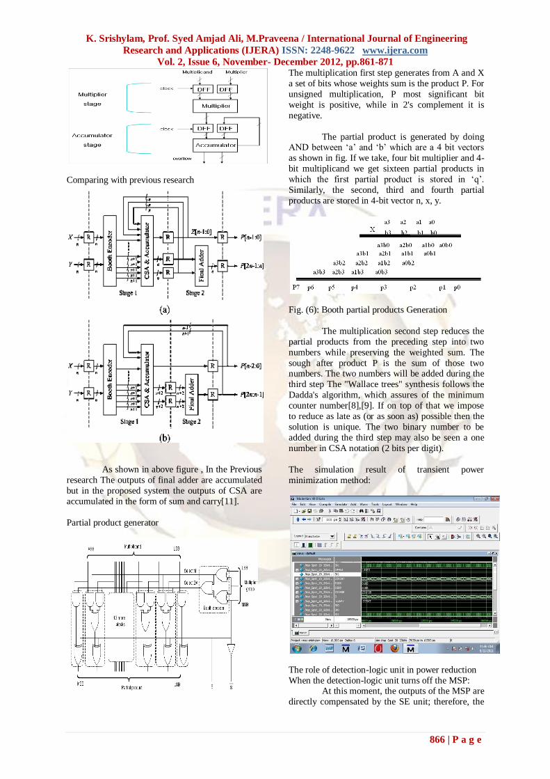
Comparing with previous research
As shown in above figure , In the Previous
research The outputs of final adder are accumulated
but in the proposed system the outputs of CSA are
accumulated in the form of sum and carry[11].
Partial product generator
The multiplication first step generates from A and X
a set of bits whose weights sum is the product P. For
unsigned multiplication, P most significant bit
weight is positive, while in 2's complement it is
negative.
The partial product is generated by doing AND between ‗a‘ and ‗b‘ which are a 4 bit vectors
as shown in fig. If we take, four bit multiplier and 4-
bit multiplicand we get sixteen partial products in
which the first partial product is stored in ‗q‘.
Similarly, the second, third and fourth partial
products are stored in 4-bit vector n, x, y.
Fig. (6): Booth partial products Generation
The multiplication second step reduces the
partial products from the preceding step into two
numbers while preserving the weighted sum. The
sough after product P is the sum of those two numbers. The two numbers will be added during the
third step The "Wallace trees" synthesis follows the
Dadda's algorithm, which assures of the minimum
counter number[8],[9]. If on top of that we impose
to reduce as late as (or as soon as) possible then the
solution is unique. The two binary number to be
added during the third step may also be seen a one
number in CSA notation (2 bits per digit).
The simulation result of transient power
minimization method:
The role of detection-logic unit in power reduction
When the detection-logic unit turns off the MSP: At this moment, the outputs of the MSP are
directly compensated by the SE unit; therefore, the

K. Srishylam, Prof. Syed Amjad Ali, M.Praveena / International Journal of Engineering
Research and Applications (IJERA) ISSN: 2248-9622 www.ijera.com
Vol. 2, Issue 6, November- December 2012, pp.861-871
867 | P a g e
time saved from skipping the computations in the
MSP circuits shall cancel out the delay caused by
the detection-logic unit.
When the detection-logic unit turns on the MSP:
The MSP circuits must wait for the notification of
the detection-logic unit to turn on the data latches to
let the data in. Hence, the delay caused by the detection-logic unit will contribute to the delay of
the whole combinational circuitry, i.e., the16-bit
adder/subtractor in this design example.
When the detection-logic unit remains its decision:
No matter whether the last decision is turning on or
turning off the MSP, the delay of the detection logic
is negligible because the path of the combinational
circuitry (i.e., the 16-bit adder/subtractor in this
design example) remains the same. From the
analysis earlier, we can know that the total delay is
affected only when the detection-logic unit turns on
the MSP. However, the detection-logic unit should be a speed-oriented design[2]. When the SPST is
applied on combinational circuitries, we should first
determine the longest transitions of the interested
cross sections of each combinational circuitry,which
is a timing
characteristic and is also related to the adopted
technology. The longest transitions can be obtained
from analyzing the timing differences between the
earliest arrival and the latest arrival signals of the
cross sections of a combinational circuitry. Then, a
delay generator similar to the delay line used in the DLL.
Design unit versatile multimedia functional unit
The proposed VMFU can compute six kinds of
arithmetic operations, i.e. addition, subtraction,
multiplication, MAC, interpolation, and SAD, which
are frequently used in multimedia/DSP
computations[2].
This unit takes care of applying the SPST to the
Modified Booth Encoder,applying SPST to the Compression Tree and freezing the Switching
Activities of the Unused Circuits
Block Diagram of VMFU
Derivation of Multiplier from VMFU
The multiplier circuit can be derived from versatile
multimedia functional unit as fallows.
By setting selection bits we can
achive Multiplication process. If the selection bits
are 001 the operation is Multiplication .The below figure shows the derived version of Multiplier.
A B
Register
Zero Padding
Registe
r
Latch
Multiplexer Unit
Latch SEL[0]
SPST Modified Booth
Encoder
Zero Padding
Normal
adder
SPS
T
adde
rs
SPS
T
adde
rs
Normal
adder
Normal
adder
SPS
T adde
rs
Normal
adder
SPST Adder
Result

K. Srishylam, Prof. Syed Amjad Ali, M.Praveena / International Journal of Engineering
Research and Applications (IJERA) ISSN: 2248-9622 www.ijera.com
Vol. 2, Issue 6, November- December 2012, pp.861-871
868 | P a g e
Based on the selection values the VMFU performs
six operations this method consist of three stages
[2],[7].
1) Partial product generation
2) Partial product reduction
3) Accumulation process
If the selection bits are 100 the operation is SAD[7].
If the selection bits are 000 the operation is Addition
If the selection bits are 010 the operation is
Subtraction
If the selection bits are 110 the operation is
Interpolation
If the selection bits are 001 the operation is
Multiplication
If the selection bits are 111 the operation is MAC
Fig. (7): Chip micrograph of the SPST equipped
VMFU
Fig. (8): The power minimization by using SPST
equipped VMFU
Design Unit Multi Transform coding (ETD)
The efficient multi transform coding
(ETD) is generally used for video processing applications in this technique the SPST adders are
merged with multiprocessing elements (MPE).
Hence we can reduce the power and save the time.
Generally these SPST adders equipped in alternate
stages because the nice occurred in the first stage is
eliminated by the next stage.
Spst equipped multi transform coding:
By combining spst and ETD ,we can get good
results.the below diagram shows the above
case.Here we discussed the three design units of
DSP/Multimedia area.
Fig. (9): Chip micrograph of the SPST-ETD
K. Srishylam, Prof. Syed Amjad Ali, M.Praveena / International Journal of Engineering
Research and Applications (IJERA) ISSN: 2248-9622 www.ijera.com
Vol. 2, Issue 6, November- December 2012, pp.861-871
869 | P a g e
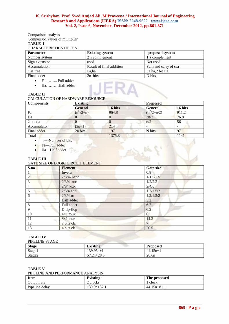
Comparison analysis
Comparison values of multiplier
TABLE I
CHARACTERISTICS OF CSA
Parameter Existing system proposed system
Number system 2‘s complement 1‘s complement
Sign extension used Not used
Accumulation Result of final addition Sum and carry of csa
Csa tree Fa,ha Fa,ha,2 bit cla
Final adder 2n bits N bits
Fa …….. Full adder
Ha……….Half adder
TABLE II
CALCULATION OF HARDWARE RESOURCE
Components Existing Proposed
General 16 bits General 16 bits
Fa (n2 /2+n) 964.8 (n2/2+n/2) 911.2
Ha 0 0 3n/2 76.8
2 bit cla 0 0 n/2 56
Accumulator (2n+1) 214 - -
Final adder 2n bits 197 N bits 97
Total 1375.8 1141
n----Number of bits
Fa—Full adder
Ha—Half adder
TABLE III GATE SIZE OF LOGIC CIRCUIT ELEMENT
S.no Element Gate size
1 Inveter 0.8
2 2/3/4- nand 1/1.5/2.5
3 2/3/4- nor 1/2/2.2
4 2/3/4-xor 2/4/6
5 2/3/4-and 1.2/1.5/2
6 2/3/4-or 1.2/1.5/2
7 Half adder 3.2
8 Full adder 6.7
9 D flp-flop 6.2
10 4×1 mux 6
11 8×1 mux 14.2
12 2 bits cla 7
13 4 bits cla 20.5
TABLE IV
PIPELINE STAGE
Stage Existing Proposed
Stage1 139.95n+1 44.15n+1
Stage2 57.2n+28.5 28.6n
TABLE V
PIPELINE AND PERFORMANCE ANALYSIS
Item Existing The proposed
Output rate 2 clocks 1 clock
Pipeline delay 139.9n+87.1 44.15n+81.1

K. Srishylam, Prof. Syed Amjad Ali, M.Praveena / International Journal of Engineering
Research and Applications (IJERA) ISSN: 2248-9622 www.ijera.com
Vol. 2, Issue 6, November- December 2012, pp.861-871
870 | P a g e
TABLE VI
NORMALIZED CAPACITANCE AND GATE DELAY
Gate Comment Capacitance Gate delay
Inverter - 3 T+c
8×1 mux 4-level logic 4 35.2+t+c
D –f/f Slave delay 4 16.1+t+c
1 bit fa Input-to sum 12 39.6+t+c
1 bit fa Input –to-carry 12 38.7+t+c
2 bit cla Input-to sum 12 64.9+t+c
2 bit cla Input-to-carry 16 53.9+t+c
4 bit cla Input-to sum 12 96.8+t+c
4 bit cla Input –to-carry 24 88+t+c
TABLE VII
COMPARISION BETWEEN EXISTING AND THE PROPOSED
Parameter Existing Proposed
Step1 Booth encoding Booth encoding
Step2 Csa Hybrid csa
Step3 Final addition Final addition
Step4 Accumulation ---
Critical path 915.2 536.8
Spst adder Not implemented Implemented
TABLE VIII
POWER COMPARISON BY USING TRANSIENT POWER MINIMIZATION METHOD
Frequency Power(mw) Reduction ( %)
Spst on Spst off
22 5.49 7.57 27.48
50 12.05 16.59 27.37
100 24.18 33.25 27.28
Conclusion In this paper, we discussed the
implementation of modified booth algorithm,
hybrid CSA and transient minimization power
techniques for the design units multiplier, VMFU
and ETD. By using modified booth encoding
technique we can increase the speed of the system
and by using Power transient minimization method
we can reduce the power up to 24%. By combining CSA and accumulation process we can form a
hybrid CSA, which is the most suitable application
of multiplier.
Future scope
By using Transient power minimization method,
we can reduce the power consumption. But this
technique increases the chip area, due to
incorporation fo dtection unit. If we suppress the
LSB power also we can further decrease the power
consumption. By applying Alpha power theorem
and LSB power minimization technique we can
compensate the Augumentation of Area.
References [1] New vlsi architecture of parallel multiplier-
accumulator based on radix-2 modified
booth algorithm
Ho Seo and Dong-Wook Kim,IEEE
Volume 18,No2 Feb 2010
[2] A Spurious power suppression Technique
for multimedia/Dsp applications,IEEE
Transations,Vol 56,No.1, Kuan-Hung
Chen,Yuan-Sun Chu.
[3] C. S. Wallace, ―A suggestion for a fast
multiplier,‖ IEEE Trans. Electron
Comput., vol. EC-13, no. 1, pp. 14–17,
Feb. 1964.
[4] A. R. Cooper, ―Parallel architecture
modified Booth multiplier,‖ Proc. Inst.
Electr. Eng. G, vol. 135, pp. 125–128,
1988. [5] N. R. Shanbag and P. Juneja, ―Parallel
implementation of a 4�4-bit multiplier using modified Booth‘s algorithm,‖ IEEE
J. Solid-State Circuits,vol. 23, no. 4, pp.
1010–1013, Aug. 1988.
[6] J. Fadavi-Ardekani, ―M�N Booth encoded multiplier generator using
optimizedWallace trees,‖ IEEE Trans.
Very Large Scale Integr. (VLSI)Syst., vol.
1, no. 2, pp. 120–125, Jun. 1993.
[7] N. Ohkubo, M. Suzuki, T. Shinbo, T.
Yamanaka, A. Shimizu, K.Sasaki, and Y.
Nakagome, ―A 4.4 ns CMOS 54�54 multiplier using pass-transistor
multiplexer,‖ IEEE J. Solid-State Circuits,
vol. 30, no.3, pp. 251–257, Mar. 1995.

K. Srishylam, Prof. Syed Amjad Ali, M.Praveena / International Journal of Engineering
Research and Applications (IJERA) ISSN: 2248-9622 www.ijera.com
Vol. 2, Issue 6, November- December 2012, pp.861-871
871 | P a g e
[8] A. Tawfik, F. Elguibaly, and P.
Agathoklis, ―New realization and
implementation of fixed-point IIR digital
filters,‖ J. Circuits, Syst., Comput., vol. 7,
no. 3, pp. 191–209, 1997.
[9] A. Tawfik, F. Elguibaly, M. N. Fahmi, E.
Abdel-Raheem, and P.Agathoklis, ―High-speed area-efficient inner-product
processor,‖ Can. J. Electr. Comput. Eng.,
vol. 19, pp. 187–191, 1994.
[10] F. Elguibaly and A. Rayhan, ―Overflow
handling in inner-product processors,‖in
Proc. IEEE Pacific Rim Conf. Commun.,
Comput., Signal Process., Aug. 1997, pp.
117–120.
[11] F. Elguibaly, ―A fast parallel multiplier–
accumulator using the modified Booth
algorithm,‖ IEEE Trans. Circuits Syst.,
vol. 27, no. 9, pp.902–908, Sep. 2000. [12] A. Fayed and M. Bayoumi, ―A merged
multiplier-accumulator for high speed
signal processing applications,‖ Proc.
ICASSP, vol. 3, pp.3212–3215, 2002.
[13] P. Zicari, S. Perri, P. Corsonello, and G.
Cocorullo, ―An optimized adder
accumulator for high speed MACs,‖ Proc.
ASICON 2005, vol.2, pp. 757–760, 2005.
[14] T. Sakurai and A. R. Newton, ―Alpha-
power law MOSFET model and its
applications to CMOS inverter delay and other formulas,‖ IEEE J.Solid-State
Circuits, vol. 25, no. 2, pp. 584–594, Feb.
1990.
[15] A. D. Booth, ―A signed binary
multiplication technique,‖ Quart. J.Math.,
vol. IV, pp. 236–240, 1952.
K.SRISHYLAM received AMIE in 2007 from the Institution of
Engineers (INDIA), M.TECH from
JNTU (JAWAHARLAL NEHRU
TECHNICALUNIVERSITY). His
areas of interest includes very large
scale integration, Astro physics, Micro
electronics,Low power VLSI. Presently he is
working as a Asst.Professor in SITECH( SAGAR
INSTITUTE OF TECHNOLOGY ),Hyderabad.He
guided many research projects in VLSI
area.Currently he is doing research on implementing low power VLSI techniques in
VMFU,FIRfilters.
.
Dr.Syed Amjad Ali received B.Tech,M.Tech and
Ph.d from JNTU( Jawaharlal Nehru Technical
University).He is having 20 years of Teaching
experience. His areas of interest includes very large
scale integration, Micro electronics,Low power VLSI,Digital Image Processing.He published more
than ten research papers in reputed
jounrnals.Presently he is working as a Professor at
Lords Institute of Engineering and
Technology,Hyderabad.
M.PRAVEENA received
B.TECH in 2008 from Srikrishna
Devaraya University and pursuing
M.TECH from JNTU(Jawaharlal
Nehru Technical University),
Anathapur. Her areas of interest
includes very large scale integration, Micro
electronics,Low power VLSI. She guided many
research projects for Engineering students .She is
working as a part time Lecturer in Sagar Institute
of Engineering and Technology(SITECH)Hyd.


![[PPT]Modified Booth Multiplier - Universidad Autónoma de …galia.fc.uaslp.mx/~rmariela/digital/ModifiedBooth.ppt · Web viewTitle Modified Booth Multiplier Author Dr. José Martin](https://static.fdocuments.net/doc/165x107/5b327a3d7f8b9aae458bff5a/pptmodified-booth-multiplier-universidad-autonoma-de-galiafcuaslpmxrmarieladigital.jpg)