“Implementation of Digital Fortress on FPGA -...
111
“Implementation of Digital Fortress on FPGA [A New Encryption Standard]” Major Project Report Submitted in Partial Fulfillment of the Requirements for Degree of Bachelor of Technology In Electronics & Communication Engineering By Manojkumar Parmar Pratik Shah Gaurang Upasani (03BEC060) (03BEC093) (03BEC115) Under the Guidance of Prof. N. P. Gajjar Associate Professor, IT, NUST Electronics & Communication Engineering Branch Department of Electrical Engineering Institute of Technology Nirma University of Science & Technology Ahmedabad 382 481 May 2007
Transcript of “Implementation of Digital Fortress on FPGA -...
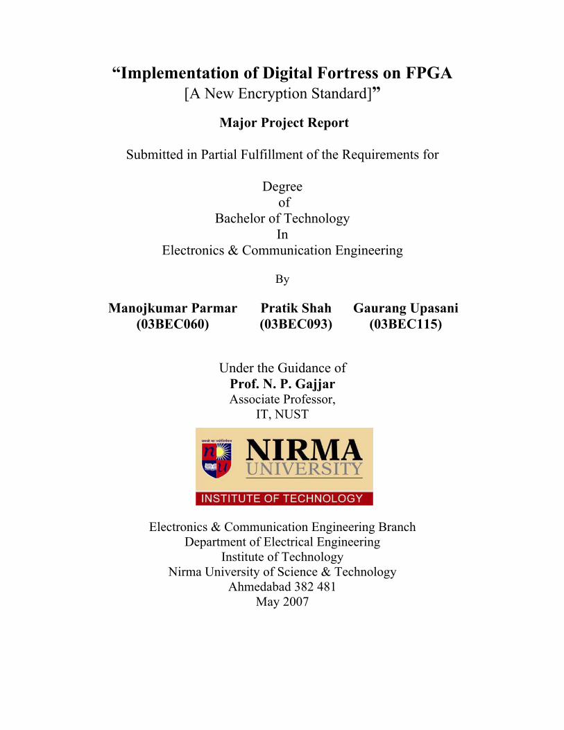
“Implementation of Digital Fortress on FPGA [A New Encryption Standard]”
Major Project Report
Submitted in Partial Fulfillment of the Requirements for
Degree of
Bachelor of Technology In
Electronics & Communication Engineering
By
Manojkumar Parmar Pratik Shah Gaurang Upasani (03BEC060) (03BEC093) (03BEC115)
Under the Guidance of Prof. N. P. Gajjar Associate Professor,
IT, NUST
Electronics & Communication Engineering Branch Department of Electrical Engineering
Institute of Technology Nirma University of Science & Technology
Ahmedabad 382 481 May 2007
CERTIFICATE
This is to certified that the major project report entitled “Implementation of Digital
Fortress on FPGA [New Standard for Encryption]” submitted by Mr.
Manojkumar Parmar (03BEC060), Mr. Pratik Shah (03BEC093) and Mr.
Gaurang Upasani (03BEC115) towards the partial fulfillment of the requirements
for semester – VIII of Bachelors of Technology (Electronics and Communications
Engineering) of Nirma University of Science and Technology, Ahmedabad for the
year 2007, is the record of work carried out by them under our supervision and
guidance. The work submitted has in our opinion has reached a level required for
being accepted for examination. The results embodied in this Project work to the best
of our knowledge have not been submitted to any other university or Institute for
award of any degree or diploma.
Project Guide:
Prof. N. P. Gajjar
Associate Professor,
EC Engineering,
Institute of Technology,
Nirma University.Ahmedabad
Head of Department:
Prof. A. S. Ranade
Electrical Department,
Institute of Technology,
Nirma University.Ahmedabad
I

Acknowledgement
“Sometimes our light goes out,
but is blown into flame by another human being,
I owe deepest thanks to those
who have rekindled this light.”
We are very grateful to the Foundation for Advancement of Education and Research
(FAER) and Motorola Ltd for considering the potential of this project to be a part of
Motorola Scholar Contest-2007 and sponsoring the project.
We are thankful towards the Department of Electronics & communication, Institute of
Technology, Nirma University, Ahmedabad for their generous help & support.
We would like to express their gratitude towards the DSP-VLSI group of Department
of Electronics & communication, Institute of Technology, Nirma University of
Science & Technology, Ahmedabad under which the project was carried out.
We would like to thank Prof. N. P. Gajjar for supervising and guiding the project and
also for nurturing our skills & to drive our minds in the directions such that we are
able to complete our project. Also we would like to thank Prof. A. B. Patel (Director,
IT, NUST), Dr. H. V. Trivedi (Head of Academic Research), Prof. A. S. Ranade
(HOD, EE), Dr. N. M. Devashrayee (Coordinator - PG, VLSI Design, EC); Dr. M. D.
Desai (Professor, IC Department & Former HOD, EE), Prof. Y. N. Trivedi, Mrs.
Neeti Avsatthi and the colleague students of Institute of Technology, Nirma
University for their valuable comments and reviews.
We are grateful towards the Mr. Dan Brown, the author of book “Digital Fortress” for
giving such a wonderful idea through the book & also for such a good book.
Last but not the least; we are very thankful to the Almighty who blessed them with the
zeal to work hard.
Gaurang Upasani Manojkumar Parmar Pratik Shah
II

ABSTRACT
Digital Fortress is proposed cryptosystem to fulfill the requirement of modern
communication system which demands low computation power, faster execution and
immunity towards attack. Authors have proposed the algorithm, built on the base of
Vernam’s One Time Pad with the help of Rotating Key Function, Permuted XORing,
etc. The algorithm has the blend of non-linearity and linearity. Rotating Key Function
is based on modulo operator along with algebraic equation to generate the randomize
Key having the length same as data from the finite small two user Keys. Permuted
XORer performs the operation on Plaintext and calculated randomized Key to
generate Ciphertext. It employs first Rotating Permutation then Modified XORing and
at the end Rotating Odd Shifter, operation performed in this suggested by name it self.
This algorithm employs all the function in primitive format for analysis purpose. The
added advantage of proposed algorithm is that all of its functional blocks are
invertible in nature and hence no separate decryption algorithm is required. All in all,
it has ability to resist most of the existing computationally efficient crypto-attack
which make it more immune to the cryptanalysis. Authors have implemented this
algorithm on VHDL and verified it on Xilinx Virtex XCV300 FPGA and the
immunity against different attacks is verified using CrypTool software. To deploy this
algorithm in commercial field certain recursivity is included at cost of little computing
power as employed in most of the encryption standard.
In a nutshell, this algorithm has ability to open new era in the field of cryptosystems
having perfect secrecy with finite length of Key which was day-dream in past but
today it exist with name of Digital Fortress.
III
CONTENTS
Certificate IAcknowledgement IIAbstract IIIList of Figures VIIList of Tables IX
1 Introduction 11.1 Overview of Project 11.2 Motivation & Affiliation 1
1.2.1 Motivation 11.2.2 Affiliation 2
1.3 Aim 21.4 Project Scheduling 21.5 Report organization 4
2 Introduction to Cryptography 62.1 Cryptography 62.2 History of Cryptography and Cryptanalysis 82.3 Modern Cryptography 12
2.3.1 Symmetric Cryptography 122.3.2 Public-Key Cryptography 13
2.4 Cryptanalysis 152.5 Cryptographic Primitives 172.6 Cryptographic Protocols 172.7 Legal Issues Involving Cryptography 18
2.7.1 Prohibitions 182.7.2 NSA Involvement 19
2.8 Need of Cryptography 20
3 Cryptosystems & Issues 223.1 Vernam’s OTP 22
3.1.1 Issues with Vernam’s OTP 253.2 DES 25
3.2.1 Issues with DES 283.2 Random Rotated XOR 29
3.3.1 Issues with Random Rotated XOR 323.4 AES 33
3.4.1 Issues with AES 35
IV

4 Introduction to Digital Fortress 364.1 Algorithm for Encryption 364.2 Segmenter 374.3 Unique Shifter 374.4 Permuted XORer 394.5 Bit Distributor 404.6 Algorithm for Decryption 404.7 Implementation 40
4.7.1 Pseudo Code 404.7.2 Notations 42
4.8 Cryptanalysis of Digital Fortress 434.9 Protocol Requirement 43
5 Simulation & Analysis 445.1 MATLAB 44
5.1.1 Digital Fortress 445.1.2 AES 465.1.3 Comparison of Digital Fortress with AES 48
5.2 Cryptool 48
6 Design Overview 516.1 Digital Fortress 516.2 PISO 556.3 Rotating Permuter 576.4 SIPO 626.5 Unique Shifter 656.6 Frequency Divider 67
7 Analysis of Design 707.1 RTL 70
7.1.1 Digital Fortress 707.1.2 PISO 717.1.3 Frequency Divider 717.1.4 Rotating Permuter 727.1.5 SIPO 727.1.6 Unique Shifter 73
7.2 Synthesis Report 737.3 Test bench 78
7.3.1 Fixed Frequency mode 787.3.2 Variable Frequency Mode 79
7.4 Implementation 807.4.1 Routed Design 80
V
7.4.2 Floor Planner 807.4.3 Footprints of IOBs 81
8 Testing, Analysis & Comparison 828.1 Testing and Analysis 828.2 Comparison 84
8.2.1 DF V/S Rest of Crypto World 848.3 Problems & Solutions 86
8.3.1 Strengths 868.3.2 Difficulties Faced 868.3.3 Proposed Solutions 86
9 Conclusion, Applications & Future Scope 88
10 References 8910.1 Internet Resources 8910.2 Books, Journals, Articles 9010.3 Research Papers 9110.4 Publications 93
Appendix I EDA Software & Hardware A-1Appendix II VSIM Scripts for Simulation A-2Appendix III HDL Code & Test bench A-5
VI
LIST OF FIGURES
Figure 1.4.1 Gantt Chart of Project schedule 3
Figure 2.1.1 German Lorenz cipher machine 6
Figure 2.1.2 Basic Encryption Models 7
Figure 2.2.1 Scytale of ancient Greece, a rod 10
Figure 2.2.2 Enigma machine 10
Figure 2.3.1 Distribution of Cryptography Techniques 12
Figure 2.9.1 Cryptography in Modern communications 21
Figure 3.2.1 The functional block diagram of DES 26
Figure 3.3.1 Left (A) and right (B) bit rotations, the place the bit indicated
by the tail of the arrow in front of the bit pointed to by the
arrow.
30
Figure 3.3.2 A sample RRX packet structure. 31
Figure 3.4.1 Block diagram of AES 33
Figure 3.4.2 Functional Block diagram of AES 34
Figure 4.1.1 Block diagram of Digital Fortress algorithm 37
Figure 4.3.1 Block diagram of Change in Coefficients between two
successive blocks
38
Figure 5.1.1.1 Continuous Data in 8 Byte Format of Plaintext, Key &
Ciphertext for Digital Fortress
45
Figure 5.1.1.2 Histogram Representation of Plaintext, Key & Ciphertext for
Digital Fortress
45
Figure 5.1.1.3 Spectrum of Plaintext, Key & Ciphertext for Digital Fortress 46
Figure 5.1.2.1 Continuous Data in 8 Byte Format of Plaintext, Key &
Ciphertext for AES
47
Figure 5.1.2.2 Histogram Representation of Plaintext, Key & Ciphertext
for AES
47
Figure 5.1.2.3 Spectrum of Plaintext, Key & Ciphertext for AES 47
VII
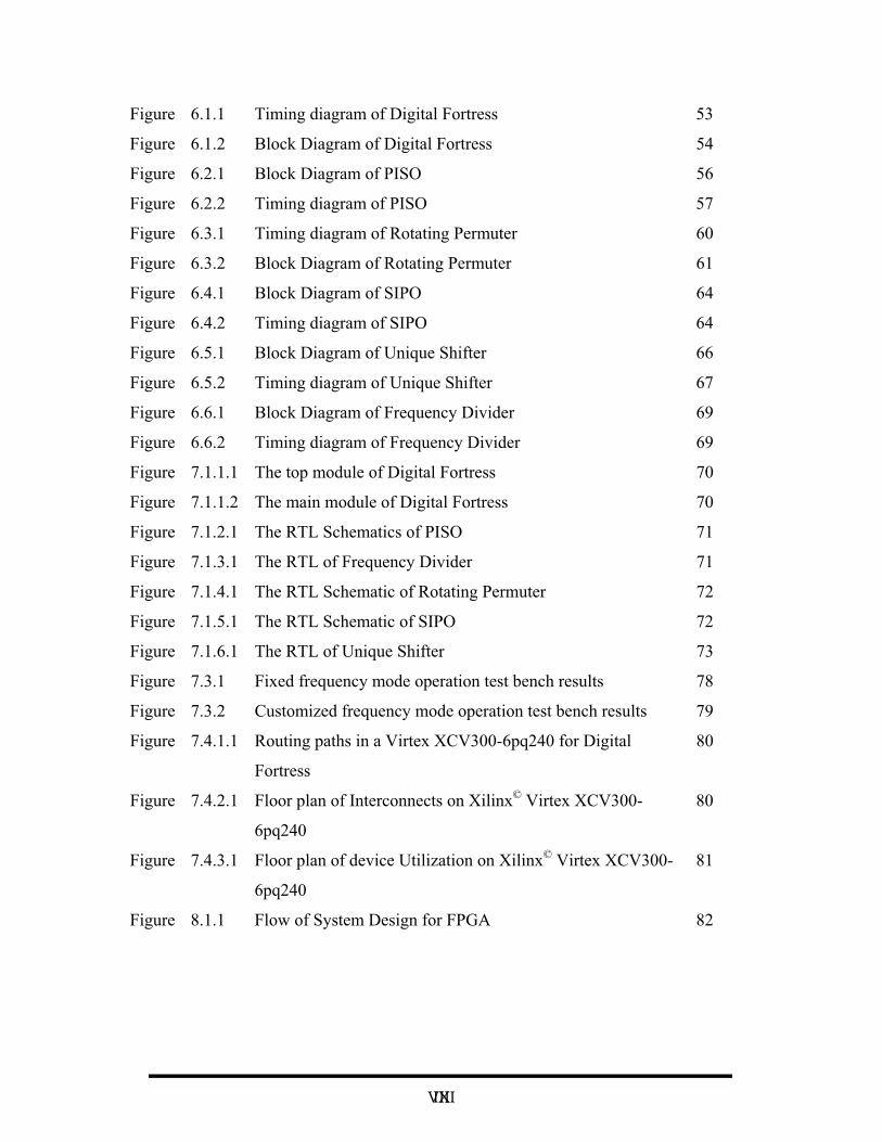
Figure 6.1.1 Timing diagram of Digital Fortress 53
Figure 6.1.2 Block Diagram of Digital Fortress 54
Figure 6.2.1 Block Diagram of PISO 56
Figure 6.2.2 Timing diagram of PISO 57
Figure 6.3.1 Timing diagram of Rotating Permuter 60
Figure 6.3.2 Block Diagram of Rotating Permuter 61
Figure 6.4.1 Block Diagram of SIPO 64
Figure 6.4.2 Timing diagram of SIPO 64
Figure 6.5.1 Block Diagram of Unique Shifter 66
Figure 6.5.2 Timing diagram of Unique Shifter 67
Figure 6.6.1 Block Diagram of Frequency Divider 69
Figure 6.6.2 Timing diagram of Frequency Divider 69
Figure 7.1.1.1 The top module of Digital Fortress 70
Figure 7.1.1.2 The main module of Digital Fortress 70
Figure 7.1.2.1 The RTL Schematics of PISO 71
Figure 7.1.3.1 The RTL of Frequency Divider 71
Figure 7.1.4.1 The RTL Schematic of Rotating Permuter 72
Figure 7.1.5.1 The RTL Schematic of SIPO 72
Figure 7.1.6.1 The RTL of Unique Shifter 73
Figure 7.3.1 Fixed frequency mode operation test bench results 78
Figure 7.3.2 Customized frequency mode operation test bench results 79
Figure 7.4.1.1 Routing paths in a Virtex XCV300-6pq240 for Digital
Fortress
80
Figure 7.4.2.1 Floor plan of Interconnects on Xilinx© Virtex XCV300-
6pq240
80
Figure 7.4.3.1 Floor plan of device Utilization on Xilinx© Virtex XCV300-
6pq240
81
Figure 8.1.1 Flow of System Design for FPGA 82
VIIIIX
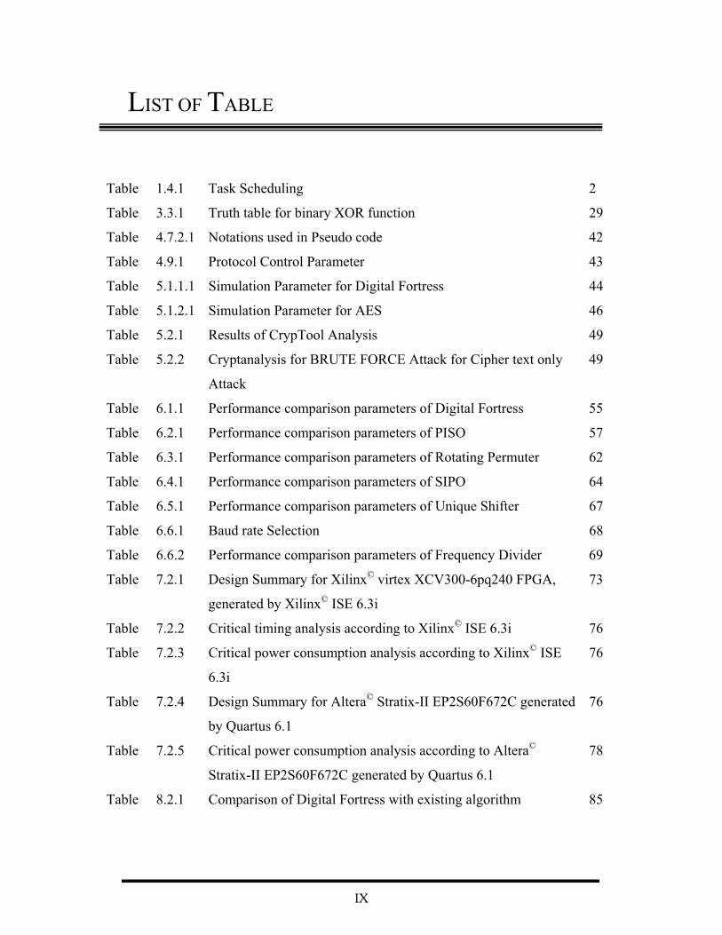
LIST OF TABLE
Table 1.4.1 Task Scheduling 2
Table 3.3.1 Truth table for binary XOR function 29
Table 4.7.2.1 Notations used in Pseudo code 42
Table 4.9.1 Protocol Control Parameter 43
Table 5.1.1.1 Simulation Parameter for Digital Fortress 44
Table 5.1.2.1 Simulation Parameter for AES 46
Table 5.2.1 Results of CrypTool Analysis 49
Table 5.2.2 Cryptanalysis for BRUTE FORCE Attack for Cipher text only
Attack
49
Table 6.1.1 Performance comparison parameters of Digital Fortress 55
Table 6.2.1 Performance comparison parameters of PISO 57
Table 6.3.1 Performance comparison parameters of Rotating Permuter 62
Table 6.4.1 Performance comparison parameters of SIPO 64
Table 6.5.1 Performance comparison parameters of Unique Shifter 67
Table 6.6.1 Baud rate Selection 68
Table 6.6.2 Performance comparison parameters of Frequency Divider 69
Table 7.2.1 Design Summary for Xilinx© virtex XCV300-6pq240 FPGA,
generated by Xilinx© ISE 6.3i
73
Table 7.2.2 Critical timing analysis according to Xilinx© ISE 6.3i 76
Table 7.2.3 Critical power consumption analysis according to Xilinx© ISE
6.3i
76
Table 7.2.4 Design Summary for Altera© Stratix-II EP2S60F672C generated
by Quartus 6.1
76
Table 7.2.5 Critical power consumption analysis according to Altera©
Stratix-II EP2S60F672C generated by Quartus 6.1
78
Table 8.2.1 Comparison of Digital Fortress with existing algorithm 85
IX
1. INTRODUCTION
1.1 Overview of Project
Title of the Project: Implementation of Digital Fortress on FPGA
[The New Standard for Data Encryption]
Area: Security of data transmission in network
Type of Project: Technology/Standard development
Brief Description: The project is all about designing a new encryption protocol,
under which the main aim is to design a new encryption
algorithm and to check its functionalities in MATLAB and
then comparing the results with the existing encryption
protocols like AES and DES. Then implementing a VHDL
code for the same and discuss the issues related to the
hardware implementation on Xilinx and Quartus FPGAs. A
comparison of hardware implementation of AES, DES and
Digital Fortress is done.
1.2 Motivation and Affiliation
1.2.1 Motivation
� The main source of motivation behind the development of the algorithm is the
famous novel “DIGITAL FORTRESS” written by DAN BROWN
� The authors are not satisfied with the existing methods of encryption systems
� To serve the goal of perfect secrecy
� To provide perfect encryption at low cost and with ease of hardware realization
1

1.2.2 Affiliation
� FAER & MOTOROLA Scholar Contest -2007
The project is one of the 22 projects selected by a group of experts for the
Motorola Scholar Contest-2007 from all over India, and it is the only project
selected from Gujarat. The project expenditure is sponsored by MOTOROLA
� DSP/VLSI Group
The required resources and guidance is being provided by the DSP/VLSI Group
of Institute of Technology, Nirma University.
1.3 Aim
Design a protocol for security in network in terms of data encryption & to
implement it in hardware (FPGA) for low power consumption circuit and low
computation power for reliable communication over network
1.4 Project Scheduling
The project is scheduled between 2nd January, 2007 to 24th April, 2007. the
detailed work distribution and the duration for implementing each block is given
in table 1.4.1 and a detailed Gantt chart is given in figure 1.4.1
Table 1.4.1 Task Scheduling
IntroductionImplementation of Digital Fortress on FPGA
2
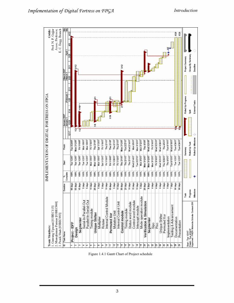
Figure 1.4.1 Gantt Chart of Project schedule
IntroductionImplementation of Digital Fortress on FPGA
3
1.5 Report Organization
Chapter 1
It gives the overview of the project including the objective and the motivation
behind picking up this definition. Also the detailed scheduling and the Gantt
chart generated by MS Project are provided.
Chapter 2
It covers the detailed introduction of cryptography, history and modern
techniques, the keywords cryptanalysis, cryptographic primitives, and
cryptographic protocols are discussed in detail, it also contains the legal issues
involving cryptography and its necessity.
Chapter 3
It discusses the issues related to the existing cryptographic techniques and the
requirement of a new algorithm.
Chapter 4
This chapter contains the detailed discussion of the new proposed algorithm
for encryption and decryption. Its pseudo code is given for reference. A
cryptanalysis is performed on the algorithm.
Chapter 5
The simulation results of the proposed algorithm on MATLAB 7.0 are
discussed. They are compared with the existing AES protocol. Also the
immunities against different attacks are analyzed using CrypTool 1.4.00
software.
Chapter 6
A detailed designing overview of all the five major blocks of the project is
given. The discussions are divided into macro blocks including the areas of
applications, features, symbol, pin descriptions, general descriptions,
functional descriptions, timing diagram and the performance on Altera and
Xilinx devices.
IntroductionImplementation of Digital Fortress on FPGA
4
Chapter 7
Detailed discussion of the test bench analysis and the synthesis report as well
as the critical timing and power consumption reports generated by the Xilinx
ISE 6.3i and the Quartus 6.1 are given. The actual floor plan and routing
diagrams are given.
Chapter 8
A flow of testing methodology is explained along with the comparisons of
Digital fortress with DES, TDES and AES.
Chapter 9
A conclusion and the future scope of work are discussed.
Chapter 10
This chapter provides the detailed list of references including internet
resources, Books, Journals, Reports, Research papers and a list of publications
by the same authors on various topics related to this project is given.
IntroductionImplementation of Digital Fortress on FPGA
5
2. INTRODUCTION TO CRYPTOGRAPHY
2.1 Cryptography
CRYPTOGRAPHY (or cryptology; derived from Greek ������� kryptós "hidden,"
and the verb ��� gráfo "write") is the study of message secrecy [1]. In modern
times, it has become a branch of information theory, as the mathematical study of
information and especially its transmission from place to place. The noted
cryptographer Ron Rivest has observed that "cryptography is about communication in
the presence of adversaries", which neatly captures one of its unique aspects as a
branch of engineering, and differences from, for instance, pure mathematics [1]. It is a
central part of several fields: information security and related issues, particularly,
authentication, and access control. One of cryptography's primary purposes is hiding
the meaning of messages, but not usually their existence [3]. Cryptography also
contributes to computer science, particularly in the techniques used in computer and
network security for such things as access control and information confidentiality [4].
Cryptography is also used in many applications encountered in everyday life;
examples include security of ATM cards, computer passwords, and electronic
commerce all depend on cryptography.
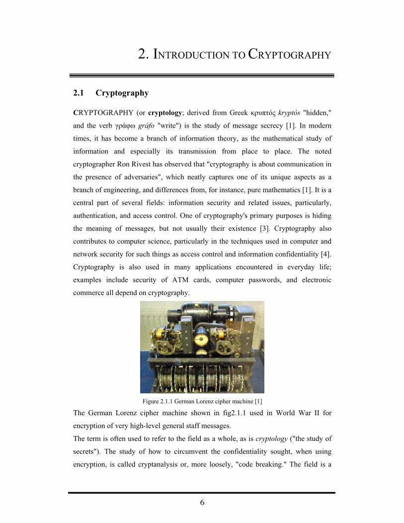
Figure 2.1.1 German Lorenz cipher machine [1]
The German Lorenz cipher machine shown in fig2.1.1 used in World War II for
encryption of very high-level general staff messages.
The term is often used to refer to the field as a whole, as is cryptology ("the study of
secrets"). The study of how to circumvent the confidentiality sought, when using
encryption, is called cryptanalysis or, more loosely, "code breaking." The field is a
6
rich source of jargon, some of it humorous. Until modern times, cryptography referred
almost exclusively only to encryption, the process of converting ordinary information
(plaintext) into unintelligible gibberish (i.e., Ciphertext). Decryption is the reverse,
moving from unintelligible Ciphertext to plaintext. A cipher (or cipher) is a pair of
algorithms which perform this encryption and the reversing decryption. The detailed
operation of a cipher is controlled both by the algorithm and, in each instance, by a
key. This is a secret parameter (known only to the communicants) for a specific
message exchange context. Keys are important as ciphers without variable keys are
trivially breakable and so rather less than useful for most purposes. Historically,
ciphers were often used directly for encryption or decryption, without additional
procedures such as authentication or integrity checks. In colloquial use, the term
"code" is often used to mean any method of encryption or concealment of meaning.
However, in cryptography, code has a more specific meaning; it means the
emplacement of a unit of plaintext (i.e., a meaningful word or phrase) with a code
word (for example, apple pie replaces attack at dawn).
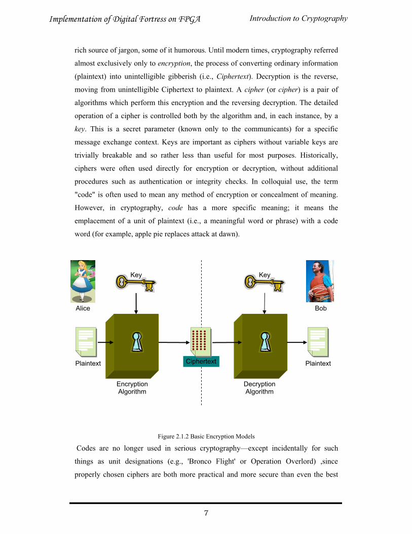
Figure 2.1.2 Basic Encryption Models
Codes are no longer used in serious cryptography—except incidentally for such
things as unit designations (e.g., 'Bronco Flight' or Operation Overlord) ,since
properly chosen ciphers are both more practical and more secure than even the best
Plaintext
EncryptionAlgorithm
DecryptionAlgorithm
Key Key
Alice Bob
CiphertextPlaintext
Introduction to CryptographyImplementation of Digital Fortress on FPGA
7
codes, and better adapted to computers as well. Some use the English terms
cryptography and cryptology interchangeably, while others use cryptography to refer
to the use and practice of cryptographic techniques, and cryptology to refer to the
subject as a field of study. In this respect, English usage is more tolerant of
overlapping meanings and word origins than are several European languages in which
meanings of cognate words are more restricted.
2.2 History of Cryptography and Cryptanalysis
Before the modern era, cryptography was concerned solely with message
confidentiality (i.e., encryption) — conversion of messages from a comprehensible
form into an incomprehensible one, and back again at the other end, rendering it
unreadable by interceptors or eavesdroppers without secret knowledge (namely, the
key needed for decryption of that message) [1]. In recent decades, the field has
expanded beyond confidentiality concerns to include techniques for message integrity
checking, sender/receiver identity authentication, digital signatures, interactive proofs,
and secure computation, amongst others. The earliest forms of secret writing required
little more than local pen and paper analogs, as most people could not read. More
literacy, or opponent literacy, required actual cryptography. The main classical cipher
types are transposition ciphers, which rearrange the order of letters in a message (e.g.
'help me' becomes 'ehpl em' in a trivially simple rearrangement scheme), and
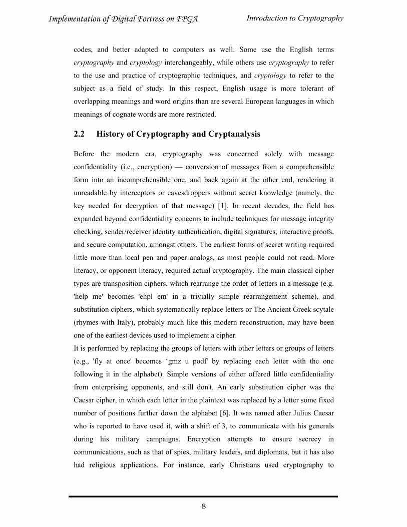
substitution ciphers, which systematically replace letters or The Ancient Greek scytale
(rhymes with Italy), probably much like this modern reconstruction, may have been
one of the earliest devices used to implement a cipher.
It is performed by replacing the groups of letters with other letters or groups of letters
(e.g., 'fly at once' becomes ‘gmz u podf' by replacing each letter with the one
following it in the alphabet). Simple versions of either offered little confidentiality
from enterprising opponents, and still don't. An early substitution cipher was the
Caesar cipher, in which each letter in the plaintext was replaced by a letter some fixed
number of positions further down the alphabet [6]. It was named after Julius Caesar
who is reported to have used it, with a shift of 3, to communicate with his generals
during his military campaigns. Encryption attempts to ensure secrecy in
communications, such as that of spies, military leaders, and diplomats, but it has also
had religious applications. For instance, early Christians used cryptography to
Introduction to CryptographyImplementation of Digital Fortress on FPGA
8
obfuscate some aspects of their religious writings to avoid the near certain persecution
they would have faced had they been less cautious; famously, 666 or in some early
manuscripts, 616, the Number of the Beast from the Christian New Testament Book
of Revelation, is sometimes thought to be a Ciphertext referring to the Roman
Emperor Nero, one of whose policies was persecution of Christians [3]. There is
record of several, even earlier, Hebrew ciphers as well [2]. Steganography (i.e., hiding
even the existence of a message so as to keep it confidential) was also first developed
in ancient times. An early example, from Herodotus, concealed a message - a tattoo
on a slave's shaved head - under the regrown hair. More modern examples of
steganography include the use of invisible ink, microdots, and digital watermarks to
conceal information.
Ciphertext produced by classical ciphers (and some modern ones) always reveal
statistical information about the plaintext, which can often be used to break them.
After the Arab discovery of frequency analysis (ca 1000CE), nearly all such ciphers
became more or less readily breakable by an informed attacker [3, 6]. Such classical
ciphers still enjoy popularity today, though mostly as puzzles. Essentially all ciphers
remained vulnerable to cryptanalysis using this technique until the invention of the
polyalphabetic cipher, most clearly by Leon Battista Alberti around the year 1467 [8].
Alberti's innovation was to use different ciphers (i.e., substitution alphabets) for
various parts of a message (often each successive plaintext letter). He also invented
what was probably the first automatic cipher device, a wheel which implemented a
partial realization of his invention. In the polyalphabetic Vigenère cipher, encryption
uses a key word, which controls letter substitution depending on which letter of the
key word is used. Despite this improvement, polyalphabetic ciphers of this type
remained partially vulnerable to frequency analysis techniques, though this was
undiscovered until the mid 1800s by Babbage [1, 3]. Although frequency analysis is a
powerful and general technique, encryption was still often effective in practice; many
a would-be cryptanalyst was unaware of the technique. Breaking a message without
frequency analysis essentially required knowledge of the cipher used, thus
encouraging espionage, bribery, burglary, defection, etc. to discover it. It was finally
recognized in the 19th century that secrecy of a cipher's algorithm is neither sensible,
nor practical, safeguard; in fact, any adequate cryptographic scheme (including
ciphers) should remain secure even if the adversary knows the cipher algorithm itself.
Secrecy of the key should alone be sufficient for confidentiality when under attack —
Introduction to CryptographyImplementation of Digital Fortress on FPGA
9
for good ciphers. This fundamental principle was first explicitly stated in 1883 by
Auguste Kerckhoffs and is generally called Kerckhoffs' principle; alternatively and
more bluntly, it was restated by Claude Shannon as Shannon's Maxim — 'the enemy
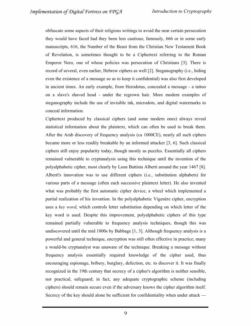
knows the system’ [5]. Various physical devices and aids have been used to assist
with ciphers.
Figure2.2.1 Scytale of ancient Greece, a rod [1]
One of the earliest may have been the scytale of ancient Greece, a rod as s
figure 2.2.1 supposedly used by the Spartans as an aid for a transposition
Cryptography. In medieval times, other aids were invented such as the cipher grille,
also used for a kind of steganography. With the invention of polyalphabetic c
became more sophisticated aids such as Alberti's own cipher disk, Johannes
Trithemius' tabular recta scheme, and Thomas
hown in
iphers
Jefferson's multi-cylinder (invented
independently by Bazeries around 1900) [5].
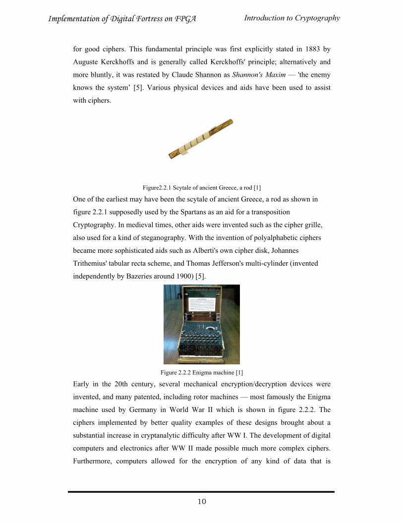
Figure 2.2.2 Enigma machine [1]
Early in the 20th century, several mechanical encryption/decryption devices were
invented, and many patented, including rotor machines — most famously the Enigma
machine used by Germany in World War II which is shown in figure 2.2.2. The
ciphers implemented by better quality examples of these designs brought about a
substantial increase in cryptanalytic difficulty after WW I. The development of digital
computers and electronics after WW II made possible much more complex ciphers.
Furthermore, computers allowed for the encryption of any kind of data that is
Introduction to CryptographyImplementation of Digital Fortress on FPGA
10
represented by computers in any binary format, unlike classical ciphers which only
encrypted written language texts, dissolving the utility of a linguistic approach to
cryptanalysis in many cases. Many computer ciphers can be characterized by their
operation on binary bit sequences (Sometimes in groups or blocks), unlike classical
and mechanical schemes, which generally manipulate traditional characters (i.e.,
letters and digits) directly. However, Computers have also assisted cryptanalysis,
which has compensated to some extent for increased cipher complexity. Nonetheless,
good modern ciphers have stayed ahead of cryptanalysis; it is usually the case that use
of a quality cipher is very efficient (i.e., fast and requiring few resources), while
breaking it requires an effort many orders of magnitude larger, making cryptanalysis
so inefficient and impractical as to be effectively impossible. Extensive open
academic research into cryptography is relatively recent — it began only in the mid-
1970s with the public specification of DES (the Data Encryption Standard) by the
NBS, the Diffie-Hellman paper, and the public release of the RSA algorithm [3,6,8].
Since then, cryptography has become a widely used tool in communications,
computer networks, and computer security generally. The present security level of
many modern cryptographic techniques is based on the difficulty of certain
computational problems, such as the integer factorization problem or the discrete
logarithm problem [9]. In many cases, there are proofs that cryptographic techniques
are secure if a certain computational problem cannot be solved efficiently. With one
notable exception “The One-Time Pad” these proofs are contingent, and thus not
definitive, but are currently the best [3]. The Enigma machine, used in several variants
by the German military between the late 1920s and the end of World War II,
implemented a complex electromechanical polyalphabetic cipher to protect sensitive
communications. Breaking the Enigma cipher at the Biuro Szyfrów, and the
subsequent large-scale decryption of Enigma traffic at Bletchley Park, was an
important factor contributing to the Allied victory in WW II [1]. Cryptographic
algorithm and system designers must also sensibly consider probable future
developments in their designs. For instance, the continued improvements in computer
processing power have increased the scope of brute-force attacks when specifying key
lengths. The potential effects of quantum computing are already being considered by
some cryptographic system designers; the announced imminence of small
implementations of these machines is making the need for this preemptive caution
fully explicit. Essentially, prior to the early 20th century, cryptography was chiefly
Introduction to CryptographyImplementation of Digital Fortress on FPGA
11
concerned with linguistic patterns [2]. Since then the emphasis has shifted, and
e use of mathematics, including aspects of
plexity, statistics, combinatory, abstract
lgebra, and number theory [1].
Modern Cryptography
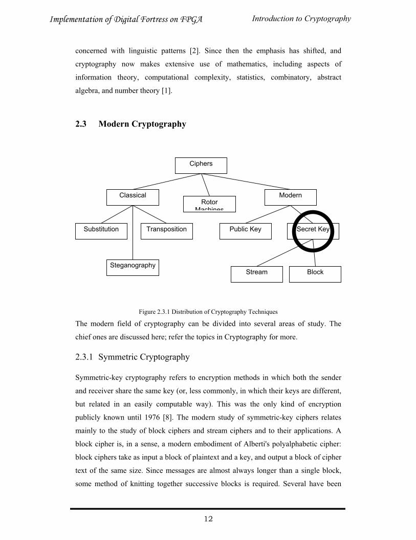
Figure 2.3.1 Distribution of Cryptography Techniques
cryptography now makes extensiv
information theory, computational com
a
2.3
Ciphers
The modern field of cryptography can be divided into several areas of study. The
chief ones are discussed here; refer the topics in Cryptography for more.
2.3.1 Symmetric Cryptography Symmetric-key cryptography refers to encryption methods in which both the sender
and receiver share the same key (or, less commonly, in which their keys are different,
but related in an easily computable way). This was the only kind of encryption
publicly known until 1976 [8]. The modern study of symmetric-key ciphers relates
mainly to the study of block ciphers and stream ciphers and to their applications. A
block cipher is, in a sense, a modern embodiment of Alberti's polyalphabetic cipher:
block ciphers take as input a block of plaintext and a key, and output a block of cipher
text of the same size. Since messages are almost always longer than a single block,
some method of knitting together successive blocks is required. Several have been
Classical ModernRotor
Machines
Substitution Transposition Public Key Secret Key
BlockStreamSteganography
Introduction to CryptographyImplementation of Digital Fortress on FPGA
12
developed, some with better security in one aspect or another than others. They are
the mode of operations and must be carefully considered when using a block cipher in
a cryptosystem. The Data Encryption Standard (DES) and the Advanced Encryption
Standard (AES) are block-cipher designs which have been designated cryptography
standards by the US government (though DES's designation was finally withdrawn
after the AES was adopted) [3, 6, 7, 8]. Despite its deprecation as an official standard,
DES (especially its still approved and much more secure triple-DES variant) remains
quite popular; it is used across a wide range of applications, from ATM encryption to
e-mail privacy and cryptographic algorithms. Many other block ciphers have been
designed and released, with considerable variation in quality. Stream ciphers, in
contrast to the 'block' type, create an arbitrarily long stream of key material, which is
combined with the plaintext bit-by-bit or character-by-character, somewhat like the
one-time pad. In a stream cipher, the output stream is created based on an internal
state which changes as the cipher operates. That state's change is controlled by the
key, and, in some stream ciphers, by the plaintext stream as well. RC4 is an example
of a well-known stream cipher; Cryptographic hash functions (often called message
digest functions) do not use keys, but are a related and important class of
cryptographic algorithms [24, 26]. They take input data (often an entire message), and
so as a one-way function. For good ones,
uce the same hash) are extremely difficult to
output a short, fixed length hash, and do
collisions (two plaintexts which prod
find. Message authentication codes (MACs) are much like cryptographic hash
functions, except that a secret key is used to authenticate the hash value on receipt.
2.3.2 Public-Key Cryptography Symmetric-key cryptosystems typically use the same key for encryption and
decryption, though this message or group of messages may have a different key than
others. A significant disadvantage of symmetric ciphers is the key management
necessary to use them securely [26]. Each distinct pair of communicating parties
must, ideally, share a different key, and perhaps each ciphertext exchanged as well.
The number of keys required increases as the square of the number of network
members, which very quickly requires complex key management schemes to keep
them all straight and secret [28]. The difficulty of establishing a secret key between
two communicating parties, when a secure channel doesn't already exist between
Introduction to CryptographyImplementation of Digital Fortress on FPGA
13
them, also presents a chicken-and-egg problem which is a considerable practical
obstacle for cryptography users in the real world. In a groundbreaking 1976 paper,
Whitfield Diffie and Martin Hellman proposed the notion of public-key (also, more
generally, called asymmetric key) cryptography in which two different but
mathematically related keys are used — a public key and a private key [26]. A public
key system is so constructed that calculation of one key (the 'private key') is
computationally infeasible from the other (the 'public key'), even though they are
necessarily related. Instead, both keys are generated secretly, as an interrelated pair.
The historian David Kahn described public-key cryptography as "the most
revolutionary new concept in the field since polyalphabetic substitution emerged in
the Renaissance". In public-key cryptosystems, the public key may be freely
distributed, while its paired rivate key must remain secret. The public key is typically
used for encryption, while the private or secret key is used for decryption. Diffie and
Hellman showed that public-key cryptography was possible by presenting the Diffie-
Hellman key exchange protocol. In 1978, Ronald Rivest, Adi Shamir, and Len
Adleman invented RSA, another public-key system [25]. In 1997, it finally
became publicly known that asymmetric key cryptography had been invented by
Whitfield Diffie and Martin Hellman, inventors of public key cryptography James H.
Ellis at GCHQ, a British intelligence organization, in the early 1970s, and that both
the Diffie- Hellman and RSA algorithms had been previously developed (by Malcolm
J. Williamson and Clifford Cocks, respectively). The Diffie-Hellman and RSA
algorithms, in addition to being the first publicly known examples of high quality
public-key ciphers, have been among the most widely used. Others include the
Cramer-Shoup cryptosystem, ElGamal encryption, and various elliptic curve
techniques. In addition to encryption, public-key cryptography can be used to
implement digital signature schemes. A digital signature is reminiscent of an ordinary
signature; they both have the characteristic that they are easy for a user to produce,
but difficult for anyone else to forge [24]. Digital signatures can also be permanently
tied to the content of the message being signed; they cannot be 'moved' from one
document to another, for any attempt will be detectable. In digital signature schemes,
there are two algorithms: one for signing, in which a secret key is used to process the
message (or a hash of the message, or both), and one for verification, in which the
matching public key is used with the message to check the validity of the signature.
RSA and DSA are two of the most popular digital signature schemes. Digital
Introduction to CryptographyImplementation of Digital Fortress on FPGA
14
signatures are central to the operation of public key infrastructures and too many
network security schemes. Public-key algorithms are most often based on the
computational complexity of “hard" problems, often from number theory. For
example, the hardness of RSA is related to the integer factorization problem, Padlock
icon from the Firefox web browser, meant to indicate a page has been sent in SSL or
TLS-encrypted protected form. More recently, elliptic curve cryptography has
developed in which security is based on number theoretic problems involving elliptic
curves [27]. Because of the difficulty of the underlying problems, most public-key
algorithms involve operations such as modular multiplication and exponentiation,
which are much more computationally expensive than the techniques used in most
block ciphers, especially with typical key sizes. As a result, public-key cryptosystems
are commonly "hybrid" systems, in which a fast high quality symmetric-key
is used for the message itself, while the relevant symmetric key
e, but encrypted using a public-key algorithm. Similarly,
encryption algorithm
is sent with theme messag
hybrid signature schemes are often used, in which a cryptographic hash function is
computed, and only the resulting hash is digitally signed.
2.4 Cryptanalysis The goal of cryptanalysis is to find some weakness or insecurity in a cryptographic
scheme, thus permitting its subversion or evasion. Cryptanalysis might be undertaken
by a malicious attacker, attempting to subvert a system, or by the system's designer
(or others) attempting to evaluate whether a system has vulnerabilities, and so it is not
inherently a hostile act [24]. In modern practice, however, cryptographic algorithms
and protocols must have been carefully examined and tested to offer any confidence
in the system's quality. Without such an examination, no confidence in a crypto-
system's quality is justified as there are few blanket, and non-contingent on
assumptions about user behavior and context, proofs of security in cryptography or
cryptanalysis. It is a commonly held misconception that every encryption method can
be broken. In connection with his WW II work at Bell Labs, Claude Shannon proved
that the one-time pad cipher is unbreakable, provided the key material is truly
random, never reused, kept secret from all possible attackers, and of equal or greater
length than the message [29, 30]. Most ciphers, apart from the one-time pad, can be
broken with enough computational effort by brute force attack, but the amount of
Introduction to CryptographyImplementation of Digital Fortress on FPGA
15
effort needed may be exponentially dependent on the key size, as compared to the
effort needed to use the cipher [23]. In such cases, effective security could be
achieved if it is proven that the effort required (i.e. 'work factor' in Shannon's terms) is
beyond the ability of any adversary. This means it must be shown that no efficient
method (as opposed to the time-consuming brute force method) can be found to break
the cipher. Since no such showing can be made currently, as of today, the one-time-
pad remains the only theoretically unbreakable cipher. There are a wide variety of
cryptanalytic attacks, and they can be classified in any of several ways. A common
distinction turns on what an attacker knows and what capabilities are available. In a
ciphertext only attack, the cryptanalyst has access only to the ciphertext (good modern
cryptosystems are usually effectively immune to ciphertext-only attacks). In a known-
plaintext attack, the cryptanalyst has access to a ciphertext and its corresponding
plaintext (or too many such pairs). In a chosen-plaintext attack, the cryptanalyst may
choose a plaintext and learn its corresponding ciphertext (perhaps many times); an
example is gardening, used by the British during WW II. Cryptanalysis of symmetric-
key ciphers typically involves looking for attacks against the block ciphers or stream
ciphers that are more efficient than any attack that could be against a perfect cipher.
For example, a simple brute force attack against DES requires one known plaintext
and 255 decryptions, trying approximately half of the possible keys, to reach a point
at which chances are better than even the key sought will have been found [8]. But
this may not be enough assurance; a linear cryptanalysis attack against DES requires
243 known plaintexts and approximately 243 DES operations [8]. This is a
considerable improvement on brute force attacks. Public-key algorithms are based on
the computational difficulty of various problems. The most famous of these is integer
factorization (e.g. the RSA algorithm is based on a problem related to factoring), but
the discrete logarithm problem is also important. Much public-key cryptanalysis
concerns numerical algorithms for solving these computational problems, or some of
them, efficiently. For instance, the best known algorithms for solving the elliptic
curve-based version of discrete logarithm are much more time consuming than the
best known algorithms for factoring, at least for problems of more or less equivalent
size [28]. Thus, other things being equal, to achieve an equivalent strength of attack
resistance, factoring based encryption techniques must use larger keys than elliptic
curve techniques. For this reason, public key cryptosystems based on elliptic curves
have become popular since their invention in the mid-1990s. While pure cryptanalysis
Introduction to CryptographyImplementation of Digital Fortress on FPGA
16
uses weaknesses in the algorithms themselves, other attacks on cryptosystems are
based on actual use of the algorithms in real devices, and are called side-channel
attacks. If a cryptanalyst has access to, say, the amount of time the device took to
encrypt a number of plaintexts or report an error in a password or PIN character, he
may be able to use a timing attack to break a cipher that is otherwise resistant to
analysis. An attacker might also study the pattern and length of messages to derive
raffic analysis,[20] and can be quite useful to
engineering, and other attacks against the
ther
vide only basic functionality. These are usually
oted as confidentiality, message integrity, authentication, and non-repudiation. Any
must be built in using combinations of these
s and assorted protocols. Such combinations are called cryptosystems and it
valuable information; this is known as t
an alert adversary. And, of course, social
personnel who work with cryptosystems or the messages they handle (e.g., bribery,
extortion, blackmail, espionage ...) may be the most productive attacks of all.
2.5 Cryptographic Primitives Much of the theoretical work in cryptography concerns cryptographic primitives —
algorithms with basic cryptographic properties and their relationship to o
cryptographic problems. For example, a one-way function is a function intended to be
easy to compute but hard to invert. In a very general sense, for any cryptographic
application to be secure (if based on such computational feasibility assumptions), one-
way functions must exist. However, if one-way functions exist, this implies that
P NP [26]. Since the P versus NP problem is currently unsolved, we don't know if
one-way functions really do exist. For instance, if one-way functions exist, then
secure pseudorandom generators and secure pseudorandom functions exist. Currently
known cryptographic primitives pro
n
other functionality in a cryptosystem
algorithm
is they which users will encounter.
2.6 Cryptographic Protocols
In many cases, cryptographic techniques involve back and forth communication
among two or more parties in space (e.g., between the home office and a branch
office) or across time (e.g., cryptographically protected backup data). The term
cryptographic protocol captures this general idea. Cryptographic protocols have been
developed for a wide range of problems, including relatively simple ones like
Introduction to CryptographyImplementation of Digital Fortress on FPGA
17
interactive proofs, secret sharing, and zero-knowledge, and much more complex ones
like electronic cash and secure multiparty computation. When the security of a good
cryptographic system fails, it is rare that the vulnerability leading to the breach will
have been in a quality cryptographic primitive. Instead, weaknesses are often mistakes
in the protocol design (often due to inadequate design procedures, or less than
thoroughly informed designers), in the implementation (e.g., a software bug), in a
failure of the assumptions on which the design was based (e.g., proper training of
those who will be using the system), or some other human error. Many cryptographic
protocols have been designed and analyzed using ad hoc methods, but they rarely
have any proof of security [27]. Methods for formally analyzing the security of
ic and more recently from
earch for the past few
, to date these tools have been cumbersome and are not widely
of
protocols, based on techniques from mathematical log
concrete security principles, have been the subject of res
decades. Unfortunately
used for complex designs [27].
2.7 Legal Issues Involving Cryptography
2.7.1 Prohibition Cryptography has long been of interest to intelligence gathering agencies and law
enforcement agencies. Because of its facilitation of privacy, and the diminution
privacy attendant on its prohibition, cryptography is also of considerable interest to
civil rights supporters. Accordingly, there has been a history of controversial legal
issues surrounding cryptography, especially since the advent of inexpensive
computers has made possible widespread access to high quality cryptography [33].
In some countries, even the domestic use of cryptography is, or has been, restricted.
Until 1999, France significantly restricted the use of cryptography domestically. In
China, a license is still required to use cryptography. Many countries have tight
restrictions on the use of cryptography. Among the more restrictive are laws in
Belarus, Kazakhstan, Mongolia, Pakistan, Russia, Singapore, Tunisia, Venezuela, and
Vietnam. In the United States, cryptography is legal for domestic use, but there has
been much conflict over legal issues related to cryptography [6, 8]. One particularly
important issue has been the export of cryptography and cryptographic software and
hardware. Because of the importance of cryptanalysis in World War II and an
expectation that cryptography would continue to be important for national security,
Introduction to CryptographyImplementation of Digital Fortress on FPGA
18
many western governments have, at some point, strictly regulated export of
cryptography. After World War II, it was illegal in the US to sell or distribute
encryption technology overseas; in fact, encryption was classified as a munition, like
tanks and nuclear weapons [3]. Until the advent of the personal computer and the
Internet, this was not especially problematic. Good cryptography is indistinguishable
from bad cryptography for nearly all users, and in any case, most of the cryptographic
ow and error prone whether good or bad.
w and computers became more widely available, high
sed), which caused concerns that NSA had deliberately made the cipher
ence efforts [3]. The whole initiative was also
ffs' principle, as the scheme included a
techniques generally available were sl
However, as the Internet gre
quality encryption techniques became well-known around the globe. As a result,
export controls came to be seen to be an impediment to commerce and to research.
2.7.2 NSA Involvement Another contentious issue connected to cryptography in the United States is the
influence of the National Security Agency in cipher development and policy [14].
NSA was involved with the design of DES during its development at IBM and its
consideration by the National Bureau of Standards as a possible Federal Standard for
cryptography. DES was designed to be secure against differential cryptanalysis, a
powerful and general cryptanalytic technique known to NSA and IBM that became
publicly known only when it was rediscovered in the late 1980s. According to Steven
Levy, IBM rediscovered differential cryptanalysis, but kept the technique secret at
NSA's request [6]. The technique became publicly known only when Biham and
Shamir re-rediscovered it some years later. The entire affair illustrates the difficulty of
determining what resources and knowledge an attacker might actually have. Another
instance of NSA's involvement was the 1993 Clipper chip affair, an encryption
microchip intended to be part of the Capstone cryptography-control initiative. Clipper
was widely criticized by cryptographers for two reasons: the cipher algorithm was
classified (the cipher, called Skipjack, was declassified in 1998 long after the Clipper
initiative lap
weak in order to assist its intellig
criticized based on its violation of Kerckho
special escrow key held by the government for use by law enforcement, for example
in wiretaps.
Introduction to CryptographyImplementation of Digital Fortress on FPGA
19
2.8 Need of Cryptography Security often requires that data be kept safe from unauthorized access. And the best
physical walls). However, physical security is not always an option (due to cost
terconnected with
that they
requirements that must be addressed:
3. Authorization: assuring th attempting to perform a function
4. Data Integrity: assuring that an object is not altered illegally.
tions of the system. For example,
urce coding and channel coding is done separately where source coding removes
inherent source redundancy, while channel coding control redundancy to combat
interference introduced over the channel. Based on this design paradigm, the signal
processing required for different functionalities in the system are design separately
and applied sequentially in a concatenated fashion.
line of defense is physical security (placing the machine to be protected behind
and/or efficiency considerations). Instead, most computers are in
each other openly, thereby exposing them and the communication channels
use.
This problem can be broken down into five
1. Confidentiality: assuring that private data remains private.
2. Authentication: assuring the identity of all parties attempting access.
at a certain party
has the permissions to do so.
5. Non-Repudiation: assuring against a party denying a data or a communication
that was initiated by them.
2.9 Cryptography in Communication A modern communication system is traditionally modeled as shown in the figure
below. As illustrated in the figure 2.9.1, the current paradigm for digital
communications systems is to perform various func
so
Introduction to CryptographyImplementation of Digital Fortress on FPGA
20
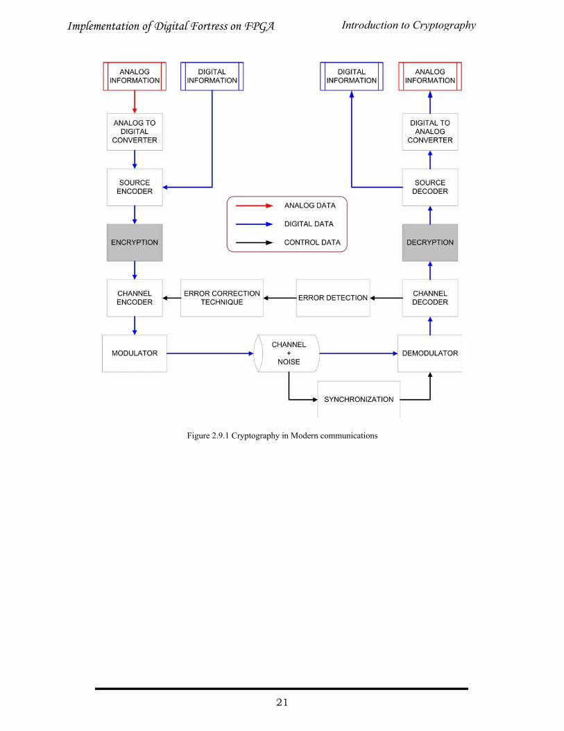
Figure 2.9.1 Cryptography in Modern communications
Introduction to CryptographyImplementation of Digital Fortress on FPGA
21
3. CRYPTOSYSTEMS & ISSUES
3.1 Vernam’s OTP As introduction to stream ciphers, and to demonstrate that a perfect cipher does exist,
we describe the Vernam’s Cipher, also known as the one-time-pad Gilbert Vernam
invented and patented his cipher in 1917 while working at AT&T [29]. The teletype
had been recently introduced, and along with this the commercial Baudot code. Now
messages were uniformly thought of as streams of zeros and ones (But the word "bit"
was not yet invented. This is due to Shannon in the 1940's.) Vernam proposed a bit-
wise exclusive or of the message stream with a truly random zero-one stream which
was shared by sender and recipient.
Example: SENDING
-------------
Message: 0 0 1 0 1 1 0 1 0 1 1 1 ...
Pad: 1 0 0 1 1 1 0 0 1 0 1 1 ...
XOR ---------------------------
Cipher: 1 0 1 1 0 0 0 1 1 1 0 0 ...
RECEIVING
----------------
Cipher: 1 0 1 1 0 0 0 1 1 1 0 0 ...
Pad: 1 0 0 1 1 1 0 0 1 0 1 1 ...
XOR ---------------------------
Message: 0 0 1 0 1 1 0 1 0 1 1 1 ...
This cipher is unbreakable in a very strong sense. The intuition is that any message
can be transformed into any cipher (of the same length) by a pad, and all
transformations are equally likely. Given a two letter message, there is a pad which
22
adds to the message to give OK, and another pad which adds to the message to give
NO. Since either of these pads is equally likely, the message is equally likely to be
OK or NO. Formal argument:
How do we capture the intuition for the security of a one-time-pad in a mathematical
proof? As we state the proof, the reader might have to be reminded of some concepts
in probability. In particular, probability distributions, conditional probability, and
independence of events. Vernam Cipher We will take as our definition of knowledge
a probability distribution.
Perfect Secrecy Proof:
Perfect Secrecy is measure for any system to possess the highest amount of security &
it is derived from probability distribution function of Plaintext, Key & cipher Key. It
states that crypto system said to possess the property of Perfect Secrecy if & only if
the Ciphertext is independent from message [30].
For analyzing this property of Digital Fortress Algorithm, assumption is taken that
Rotating Key Function generate randomize Key & consider only permuted XORing
function
P (M) - Probability distribution of plain text M
P (C) - Probability distribution of cipher text C
P (M/C) - Conditional Probability distribution of Plaintext M over Ciphertext C
P (M/C) = P (M and C) / P (C) (3.1.1)
The event (M and C) is the same as the event (M and p) where p is the pad which
equals M��C. Since the message and the pad are independent events. From Eq. 3.1.1
P (M and C) = P (M and p)
= P (M) P (p) (3.1.2)
The probability of P (C) is the probability that a message M and a pad p came
together to form C. For every message M i there is exactly one pad p i yielding C,
namely, p i = M i �C, So
Cryptosystems & IssuesImplementation of Digital Fortress on FPGA
23
P (C) = �i P (M i and p i)
= �i P(Mi) P(pi)
= (1/2n) �i P(Mi)
= 1/2n (3.1.3)
Also, P (pi) = P(p) = 1/2n (3.1.4)
So, from Eq. 3.1.3 and Eq. 3.1.4
P (C) = P (p) (3.1.5)
Substituting Eq. 3.1.5 & Eq. 3.1.2 in to Eq. 3.1.1
So, P (M/C) = P (M)
It means that knowledge about message can’t be extracted from Ciphertext because
dependency does not exist between them. A word of caution:
The conclusion that the Vernam cipher gives perfect secrecy depends on the
assumption that each pad is equally likely. If the pad is used to encipher more than
one message, this is no longer true, and the message may be discovered. It is
important that a pad once used is discarded. That is the reason for the name one-time-
pad, also known as OTP. If this warning is not heeded, the two cipher texts can be
subtracted, thus eliminating the pad. What is left is the difference of messages, which
has a distribution reflecting back on the possibility of choice of pad. This has been
known to completely break the cipher. The calculation is, c = m (+) p and c' = m' (+) p ; Implies that
c (+) c'= (m(+)p) (+) (m'(+)p)= (m(+)m') (+) (p(+)p) = m (+) m' The pad has been subtracted off. Although the distribution on pads is uniform,
P(p)=1/2n, for any p, the conditional probability of pads given a ciphertext, P(p|c), is
not [16]. It is exactly the probability of the message being m where m = c (+) p. Given
two cipher texts and the understanding that the messages must be plausible for each
ciphertext under a single pad, we can modify P(p|c) and consequently, P(m|c).
Whether this information is enough to determine the messages and the pads depends
on the situation. However, we have violated our absolute requirement for perfect
secrecy.
Cryptosystems & IssuesImplementation of Digital Fortress on FPGA
24
3.1.1 Issues with Vernam’s OTP � Length of key is same as length of data and hence the overhead of
transportation of large key is always there which consumes more bandwidth.
� If same key is used than cryptanalysis becomes very easy by taking the
difference between two messages and then applying frequency analysis.
� It is very basic cryptosystem by nature.
3.2 DES In 1972, the National Institute of Standards and Technology (called the National
Bureau of Standards at the time) decided that a strong cryptographic algorithm was
needed to protect non-classified information. The algorithm was required to be cheap,
widely available, and very secure. NIST envisioned something that would be
available to the general public and could be used in a wide variety of applications. So
they asked for public proposals for such an algorithm. In 1974 IBM submitted the
Lucifer algorithm, which appeared to meet most of NIST's design requirements. NIST
enlisted the help of the National Security Agency to evaluate the security of Lucifer.
At the time many people distrusted the NSA due to their extremely secretive
activities, so there was initially a certain degree of skepticism regarding the analysis
of Lucifer. One of the greatest worries was that the key length, originally 128 bits,
was reduced to just 56 bits, weakening it significantly. The NSA was also accused of
changing the algorithm to plant a "back door" in it that would allow agents to decrypt
any information without having to know the encryption key [6]. But these fears
proved unjustified and no such back door has ever been found. The modified Lucifer
algorithm was adopted by NIST as a federal standard on November 23, 1976. Its
name was changed to the Data Encryption Standard (DES) [31]. The algorithm
specification was published in January 1977, and with the official backing of the
government it became a very widely employed algorithm in a short amount of time.
Unfortunately, over time various shortcut attacks were found that could significantly
reduce the amount of time needed to find a DES key by brute force. And as computers
became progressively faster and more powerful, it was recognized that a 56-bit key
was simply not large enough for high security applications [26]. As a result of these
serious flaws, NIST abandoned their official endorsement of DES in 1997 and began
work on an emplacement, to be called the Advanced Encryption Standard (AES).
Cryptosystems & IssuesImplementation of Digital Fortress on FPGA
25
Despite the growing concerns about its vulnerability, DES is still widely used by
financial services and other industries worldwide to protect sensitive on-line
applications. To highlight the need for stronger security than a 56-bit key can offer,
RSA Data Security has been sponsoring a series of DES cracking contests since early
1997. In 1998 the Electronic Frontier Foundation won the RSA DES Challenge II-2
contest by breaking DES in less than 3 days. EFF used a specially developed
computer called the DES Cracker, which was developed for under $250,000 [1]. The
encryption chip that powered the DES Cracker was capable of processing 88 billion
keys per second. More recently, in early 1999, Distributed. Net used the DES Cracker
and a worldwide network of nearly 100,000 PCs to win the RSA DES Challenge III in
a record breaking 22 hours and 15 minutes. The DES Cracker and PCs combined
were testing 245 billion keys per second when the correct key was found. In addition,
it has been shown that for a cost of one million dollars a dedicated hardware device
can be built that can search all possible DES keys in about 3.5 hours [8]. This just
serves to illustrate that any organization with moderate resources can break through
DES with very little effort these days.
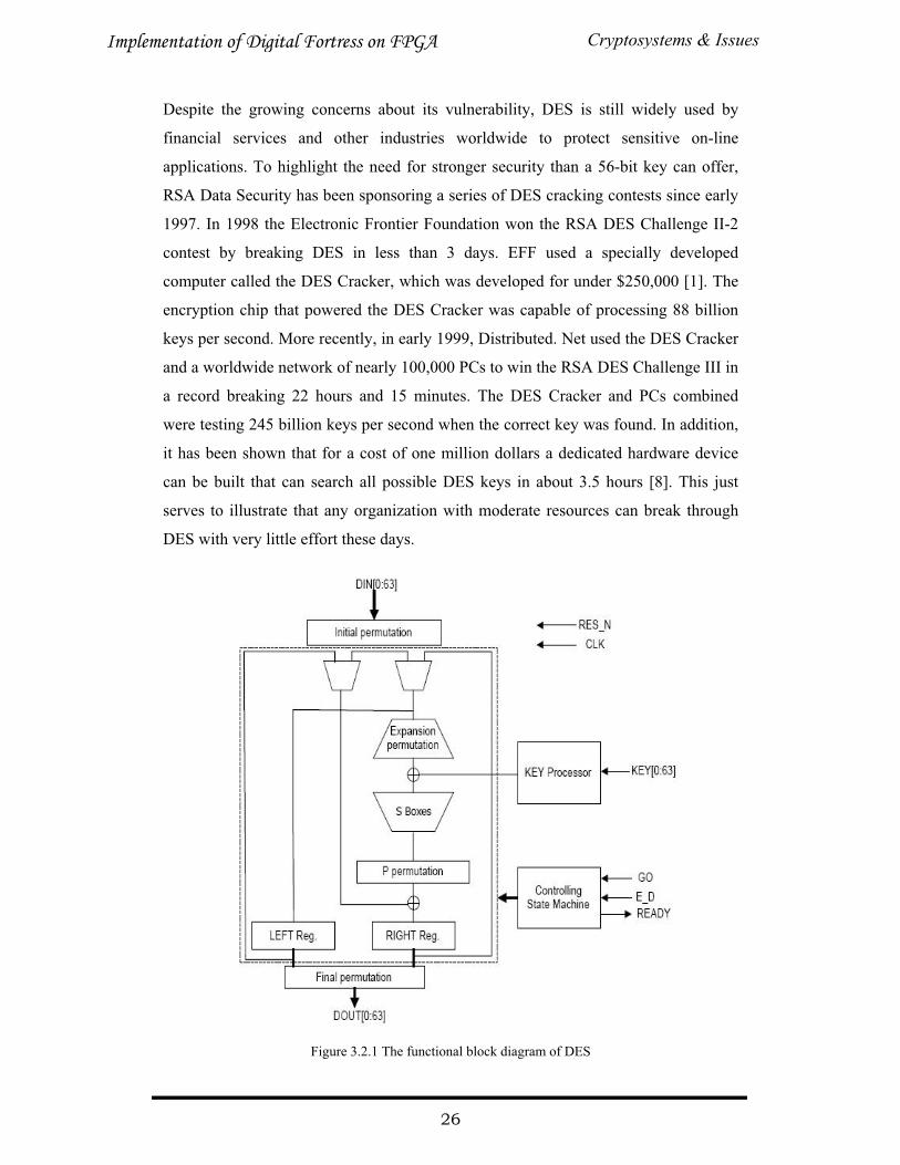
Figure 3.2.1 The functional block diagram of DES
Cryptosystems & IssuesImplementation of Digital Fortress on FPGA
26
In Depth:
DES encrypts and decrypts data in 64-bit blocks, using a 64-bit key (although the
effective key strength is only 56 bits, as explained below) and functional block
diagram of DES is shown in figure 3.2.1. It takes a 64-bit block of plaintext as input
and outputs a 64-bit block of ciphertext. Since it always operates on blocks of equal
size and it uses both permutations and substitutions in the algorithm, DES is both a
block cipher and a product cipher. DES has 16 rounds, meaning the main algorithm is
repeated 16 times to produce the ciphertext [31]. It has been found that the number of
rounds is exponentially proportional to the amount of time required to find a key
using a brute-force attack. So as the number of rounds increases, the security of the
algorithm increases exponentially. Key Scheduling:
Although the input key for DES is 64 bits long, the actual key used by DES is only 56
bits in length. The least significant (right-most) bit in each byte is a parity bit, and
should be set so that there are always an odd number of 1s in every byte. These parity
bits are ignored, so only the seven most significant bits of each byte are used,
resulting in a key length of 56 bits.
The first step is to pass the 64-bit key through a permutation called Permuted Choice
1, or PC-1 for short. The table for this is given below. Note that in all subsequent
descriptions of bit numbers, 1 is the left-most bit in the number, and n is the rightmost
bit. DES Core Function:
Once the key scheduling and plaintext preparation have been completed, the actual
encryption or decryption is performed by the main DES algorithm. The 64-bit block
of input data is first split into two halves, L and R. L is the left-most 32 bits, and R is
the right-most 32 bits. The following process is repeated 16 times, making up the 16
rounds of standard DES. We call the 16 sets of halves L[0]-L[15] and R[0]-R[15].
1. R[I-1] - where I is the round number, starting at 1 - is taken and fed into the E-Bit
Selection Table, which is like a permutation, except that some of the bits are used
more than once. This expands the number R[I-1] from 32 to 48 bits to prepare for
the next step.
Cryptosystems & IssuesImplementation of Digital Fortress on FPGA
27
2. The 48-bit R[I-1] is XORed with K[I] and stored in a temporary buffer so that
R[I-1] is not modified.
3. The result from the previous step is now split into 8 segments of 6 bits each. The
leftmost 6 bits are B[1], and the right-most 6 bits are B[8]. These blocks form the
index into the S-boxes, which are used in the next step. The Substitution boxes,
known as S-boxes, are a set of 8 two-dimensional arrays, each with 4 rows and 16
columns. The numbers in the boxes are always 4 bits in length, so their values
range from 0-15. The S-boxes are numbered S[1]-S[8].
4. Starting with B[1], the first and last bits of the 6-bit block are taken and used as an
index into the row number of S[1], which can range from 0 to 3, and the middle
four bits are used as an index into the column number, which can range from 0 to
15. The number from this position in the S-box is retrieved and stored away. This
is repeated with B[2] and S[2], B[3] and S[3], and the others up to B[8] and S[8].
At this point, you now have 8 4-bit numbers, which when strung together one after
the other in the order of retrieval, give a 32-bit result.
5. The result from the previous stage is now passed into the P Permutation.
6. This number is now XORed with L[I-1], and moved into R[I]. R[I-1] is moved
into L [I].
7. At this point we have a new L[I] and R[I]. Here, we increment I and repeat the
core function until I = 17, which means that 16 rounds have been executed and
keys K[1]-K [16] have all been used. When L[16] and R[16] have been obtained,
they are joined back together in the same fashion they were split apart (L[16] is
the left-hand half, R[16] is the right-hand half), then the two halves are swapped,
R[16] becomes the left-most 32 bits and L[16] becomes the right-most 32 bits of
the pre-output block and the resultant 64-bit number is called the pre-output.
3.2.1 Issues with DES
� DES is genuinely designed for software and for microprocessor and hence
efficient implementation of hardware is not possible until the pipelined
hardware architecture is used.
� DES uses no. of rounds for some operations so the hardware implemented
other than this part is not efficiently utilized.
� Cryptanalysis of DES is comparatively easy if proper attack is used.
Cryptosystems & IssuesImplementation of Digital Fortress on FPGA
28
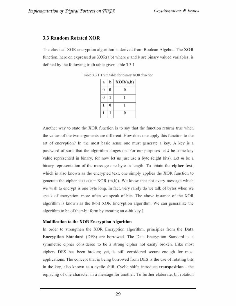
3.3 Random Rotated XOR The classical XOR encryption algorithm is derived from Boolean Algebra. The XOR
function, here on expressed as XOR(a,b) where a and b are binary valued variables, is
defined by the following truth table given table 3.3.1
Table 3.3.1 Truth table for binary XOR function
a b XOR(a,b)
0 0 0
0 1 1
1 0 1
1 1 0
Another way to state the XOR function is to say that the function returns true when
the values of the two arguments are different. How does one apply this function to the
art of encryption? In the most basic sense one must generate a key. A key is a
password of sorts that the algorithm hinges on. For our purposes let k be some key
value represented in binary, for now let us just use a byte (eight bits). Let m be a
binary representation of the message one byte in length. To obtain the cipher text,
which is also known as the encrypted text, one simply applies the XOR function to
generate the cipher text c(c = XOR (m,k)). We know that not every message which
we wish to encrypt is one byte long. In fact, very rarely do we talk of bytes when we
speak of encryption, more often we speak of bits. The above instance of the XOR
algorithm is known as the 8-bit XOR Encryption algorithm. We can generalize the
algorithm to be of then-bit form by creating an n-bit key.]
Modification to the XOR Encryption Algorithm
In order to strengthen the XOR Encryption algorithm, principles from the Data
Encryption Standard (DES) are borrowed. The Data Encryption Standard is a
symmetric cipher considered to be a strong cipher not easily broken. Like most
ciphers DES has been broken; yet, is still considered secure enough for most
applications. The concept that is being borrowed from DES is the use of rotating bits
in the key, also known as a cyclic shift. Cyclic shifts introduce transposition - the
replacing of one character in a message for another. To further elaborate, bit rotation
Cryptosystems & IssuesImplementation of Digital Fortress on FPGA
29
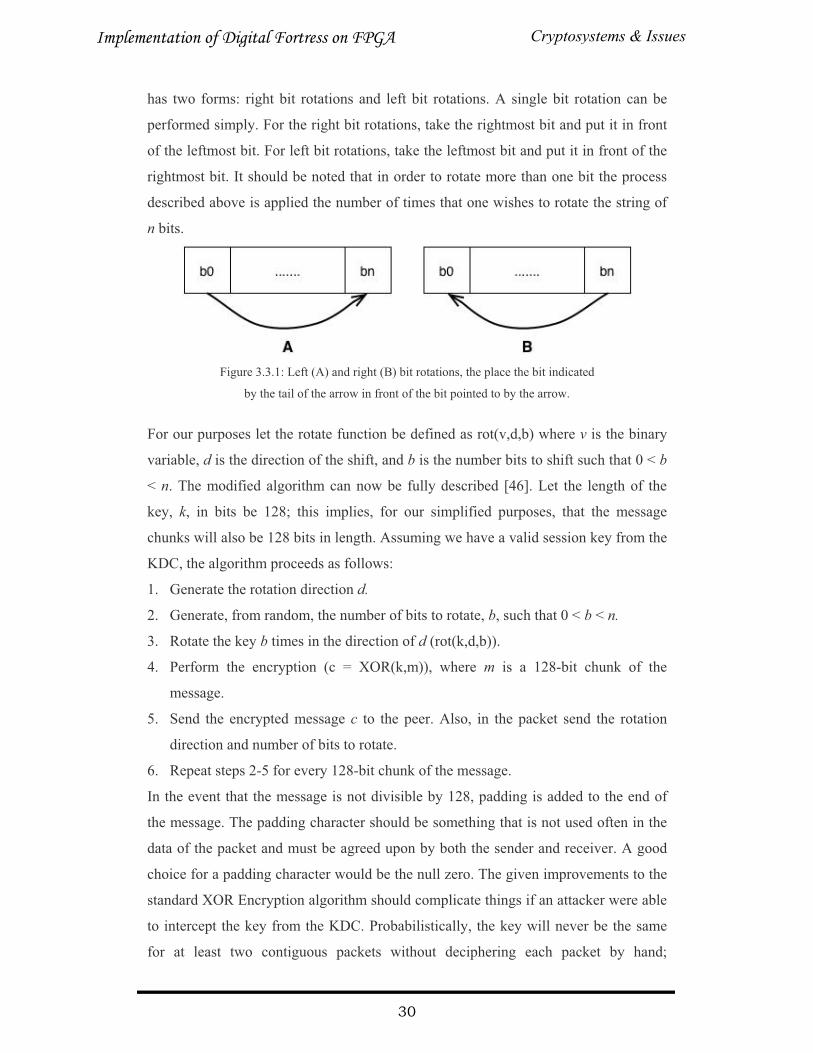
has two forms: right bit rotations and left bit rotations. A single bit rotation can be
performed simply. For the right bit rotations, take the rightmost bit and put it in front
of the leftmost bit. For left bit rotations, take the leftmost bit and put it in front of the
rightmost bit. It should be noted that in order to rotate more than one bit the process
described above is applied the number of times that one wishes to rotate the string of
n bits.
Figure 3.3.1: Left (A) and right (B) bit rotations, the place the bit indicated
by the tail of the arrow in front of the bit pointed to by the arrow.
For our purposes let the rotate function be defined as rot(v,d,b) where v is the binary
variable, d is the direction of the shift, and b is the number bits to shift such that 0 < b
< n. The modified algorithm can now be fully described [46]. Let the length of the
key, k, in bits be 128; this implies, for our simplified purposes, that the message
chunks will also be 128 bits in length. Assuming we have a valid session key from the
KDC, the algorithm proceeds as follows:
1. Generate the rotation direction d.
2. Generate, from random, the number of bits to rotate, b, such that 0 < b < n.
3. Rotate the key b times in the direction of d (rot(k,d,b)).
4. Perform the encryption (c = XOR(k,m)), where m is a 128-bit chunk of the
message.
5. Send the encrypted message c to the peer. Also, in the packet send the rotation
direction and number of bits to rotate.
6. Repeat steps 2-5 for every 128-bit chunk of the message.
In the event that the message is not divisible by 128, padding is added to the end of
the message. The padding character should be something that is not used often in the
data of the packet and must be agreed upon by both the sender and receiver. A good
choice for a padding character would be the null zero. The given improvements to the
standard XOR Encryption algorithm should complicate things if an attacker were able
to intercept the key from the KDC. Probabilistically, the key will never be the same
for at least two contiguous packets without deciphering each packet by hand;
Cryptosystems & IssuesImplementation of Digital Fortress on FPGA
30

recalculating the new key each time the attacker would not be able to penetrate the
cipher. The algorithm as presented is akin to Shannon's one time pad algorithm except
Shannon's one time pad only uses a key only once .In the described algorithm a key is
probabistically never used twice consecutively, but a key will be used again
eventually. Executing this kind of process offers a level of obfuscation. How would
one create the packet for the new, Random Rotating XOR (RRX) [40], encryption
algorithm? The data segment of the packet should be 136-bits in length. The first bit
will specify the rotation direction (0 = Left, 1 = Right), d. The next 7 bits, which in
implementation should be longer, will be representative of the number of bits to rotate
b. The final 128 bits will hold the encrypted message.
Figure 3.3.2: A sample RRX packet structure.
How good is RRX?
The strength of any encryption algorithm cannot always be accurately analyzed in the
laboratory. That being said there are two obvious flaws with the RRX algorithm. The
first major flaw is if the key were intercepted from the KDC by an attacker. The
attacker could then decrypt the messages for the rest of that session. This, however, is
complicated by the fact that the key is constantly being operated upon and therefore
dynamic. The fact that the key is dynamic does not add to the strength of the cipher in
a natural way, because it does not change the entropy. The cipher does, however,
offer a layer of obfuscation which presents a hurdle for an attacker. Entropy is defined
as a measure of randomness in the cipher. In order for an attacker to decrypt a
communication, the attacker needs to intercept all of the messages between the peers
and decrypt each packet so that the key is not operated on wrong. The second obvious
flaw is in the fact that RRX is a symmetric cipher. This means that the cipher hinges
Cryptosystems & IssuesImplementation of Digital Fortress on FPGA
31
mainly on the protection of the key. In the case of RRX this is slightly relaxed, but
still necessary. Placing the weaknesses aside, RRX does offer some protection that is
not available in most XOR based encryption methods. RRX offers the protection of a
dynamic key; this dynamic key aides in preventing an attacker, who cannot intercept
messages from a well protected KDC, from applying frequency analysis as easily,
across the collected sub-messages. Frequency Analysis is the process of determining
the percentage of the occurrence of a certain pattern in a message. These percentages,
or frequencies, are then compared against a known list of frequencies and the attacker
can guess at what the message says without knowing the key. Since, a packet of data
is so small, there does not exist a sufficient sample size to accurately use frequency
analysis. However, the algorithm can be cracked if every packet was saved and a user
was able to XOR appropriate packets together to obtain the proper key for a given
pair of packets. A rectification to this problem would be to request a new key for the
session from the KDC after a given amount of time or a statistical event becomes
highly likely. Knowing the algorithm for RRX does not allow an attacker to easily
decipher the communications because of the random nature of the key operations. If
the results of the key operations were predictable the attacker would only need to
know the given datum's placement in the sequence, provided the key had also been
intercepted a final strength that RRX has, as much as the other XOR based encryption
ciphers, is that RRX can be implemented in both hardware and software effectively.
This allows the actual hardware that supports RRX to be implemented directly on the
Network Interface Card (NIC). As far as RRX implemented as a software solution,
the program could be easily written as a tiny segment of well tuned assembly code (to
improve performance).
3.3.1 Issues with Random Rotated XOR
� It requires one central device KDC to distribute the key dynamically which
is not possible for large network.
� KDC can not generate the true random key for all the user and sometimes
these keys might be collided with each other and generate the pitfalls.
� Whole system is dependent upon KDC. If this KDC fails to perform task
or even hacked then system is of no use.
Cryptosystems & IssuesImplementation of Digital Fortress on FPGA
32
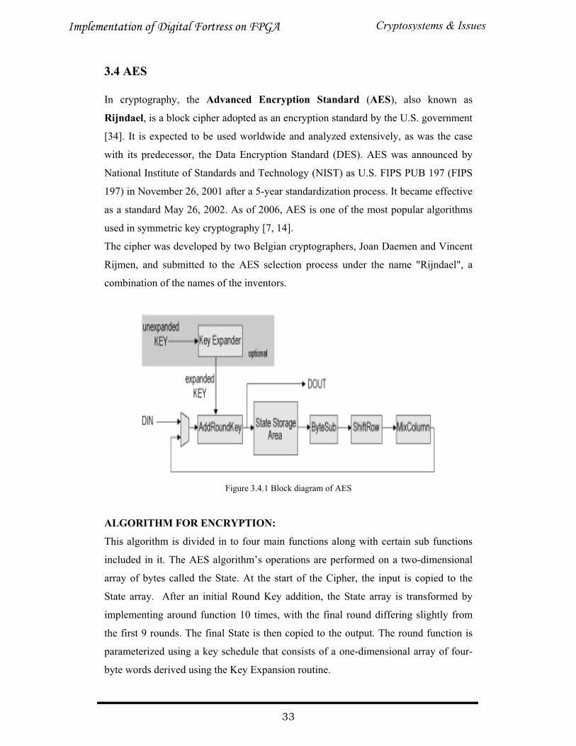
3.4 AES In cryptography, the Advanced Encryption Standard (AES), also known as
Rijndael, is a block cipher adopted as an encryption standard by the U.S. government
[34]. It is expected to be used worldwide and analyzed extensively, as was the case
with its predecessor, the Data Encryption Standard (DES). AES was announced by
National Institute of Standards and Technology (NIST) as U.S. FIPS PUB 197 (FIPS
197) in November 26, 2001 after a 5-year standardization process. It became effective
as a standard May 26, 2002. As of 2006, AES is one of the most popular algorithms
used in symmetric key cryptography [7, 14].
The cipher was developed by two Belgian cryptographers, Joan Daemen and Vincent
Rijmen, and submitted to the AES selection process under the name "Rijndael", a
combination of the names of the inventors.
Figure 3.4.1 Block diagram of AES
ALGORITHM FOR ENCRYPTION:
This algorithm is divided in to four main functions along with certain sub functions
included in it. The AES algorithm’s operations are performed on a two-dimensional
array of bytes called the State. At the start of the Cipher, the input is copied to the
State array. After an initial Round Key addition, the State array is transformed by
implementing around function 10 times, with the final round differing slightly from
the first 9 rounds. The final State is then copied to the output. The round function is
parameterized using a key schedule that consists of a one-dimensional array of four-
byte words derived using the Key Expansion routine.
Cryptosystems & IssuesImplementation of Digital Fortress on FPGA
33

AddRoundKey:
In the transformation, a Round Key is added to the State by a simple bitwise XOR
operation. Each Round Key consists of Nb words from the key schedule. Those Nb
words are each added into the columns of the State, such that [S’]=[S’] [Wround*nb+c]
for 0 c�Nb; Where [wi] are the key schedule words, and round is a value in the
range 0 round�10. In the Cipher, the initial Round Key addition occurs when round
= 0, prior to the first application of the round function.
�
�
�
Functional Diagram:
Figure 3.4.2 Functional Block diagram of AES
Subbytes:
It is a non-linear byte substitution that operates independently on each byte of the
State using a substitution table (S-box). This S-box, which is invertible, is constructed
by composing two transformations: First is to take the multiplicative inverse in the
finite field; the element {00} is mapped to itself and then apply the following affine
transformation:
for 0 �i �8 , where bi is the ith bit of the byte, and ci is the ith bit of a byte c with the
value {63} or {01100011}.
� �
ShiftRows:
In this transformation, the bytes in the last three rows of the State are cyclically
shifted over different numbers of bytes (offsets).
Cryptosystems & IssuesImplementation of Digital Fortress on FPGA
34
The first row, r = 0, is not shifted. Specifically, transformation proceeds as follows:
Where Nb is the no of columns and the shift value shift(r, Nb) depends on the row
number, r. (recall that Nb = 4): This has the effect of moving bytes to “lower”
positions in the row (i.e., lower values of c in a given row), while the “lowest” bytes
wrap around into the “top” of the row (i.e., higher values of c in a given row).
MixColumns:
The transformation operates on the State column-by-column, treating each column as
a four-term polynomial. The columns are considered as polynomials and multiplied
modulo x4 + 1 with a fixed polynomial a(x), given by s’ (x) =�a(x)� s(x) Key Expansion:
The AES algorithm takes the Cipher Key, K, and performs a Key Expansion routine
to generate a key schedule. The Key Expansion generates a total of Nb*(11) words:
the algorithm requires an initial set of Nb words, and each of the 10 rounds requires
Nb words of key data. The resulting key schedule consists of a linear array of 4-byte
words, denoted [wi], with i in the range 0 (�i < Nb*(11)).
It can be seen that the first Nk (Number of 32-bit words comprising the Cipher Key)
words of the expanded key are filled with the Cipher Key. Every following word, is
equal to the XOR of the previous word, and the word Nk positions earlier. For words
in positions that are a multiple of Nk, a transformation is applied to the previous word
prior to the XOR, followed by an XOR with a round constant word array. This
transformation consists of a cyclic shift of the bytes in a word, followed by the
application of S-box look up table.
3.4.1 Issues with AES
� AES is very complex in nature for realizing its hardware on FPGA.
� AES is iterative standard so the hardware utilization ratio is very poor in
terms of most of the time only one part of hardware is performing task.
� AES can be analyzed by differential frequency analysis with known
plaintext attack.
Cryptosystems & IssuesImplementation of Digital Fortress on FPGA
35
4. INTRODUCTION OF DIGITAL FORTRESS
Digital Fortress is proposed algorithm which is modified and enhanced version of
Vernam’s OTP [64]. In this algorithm, authors introduce certain unique function to
enhance the performance of Vernam’s OTP algorithm with small and finite length
Key. To modify original algorithm some new type of operation introduce in existing
function to get the best performance. This algorithm is divided in to four functions
named SEGMENTER, UNIQUE SHIFTER, PERMUTED XORER and BIT
DISTRIBUTOR [65]. This algorithm is classified as symmetric Key algorithm but
having the blend of linearity as well as non-linearity. It employs two Key encryption
structure instead of single Key in which one is alphanumeric Key and second one is
the numeric Key. In this algorithm, first data segment each of 8 byte is generated by
Segmenter then manipulation on Key takes place by UNIQUE SHIFTER which is
actually Rotating Key Function to generate same length of Key as of data in same
segment size. PERMUTED XORER performs operation on each segment with the
help of some functions like Rotating Permutation, Modified XORing and Rotating
Odd Shifter. PERMUTED XORER gives the encrypted data as output which can be
dumped in to image by using BIT DISTRIBUTOR so data get hided in to image and
make algorithm immune towards all attack. Proposed algorithm is viable solution for
all type of networks and it is subjected to certain modification according to the need
of networks like speed, scalability & etc.
4.1 Algorithm for Encryption
This algorithm is divided in to four main functions including certain sub functions.
The logical relation between functions is shown in figure 2 and their functionality is
as follows:
36
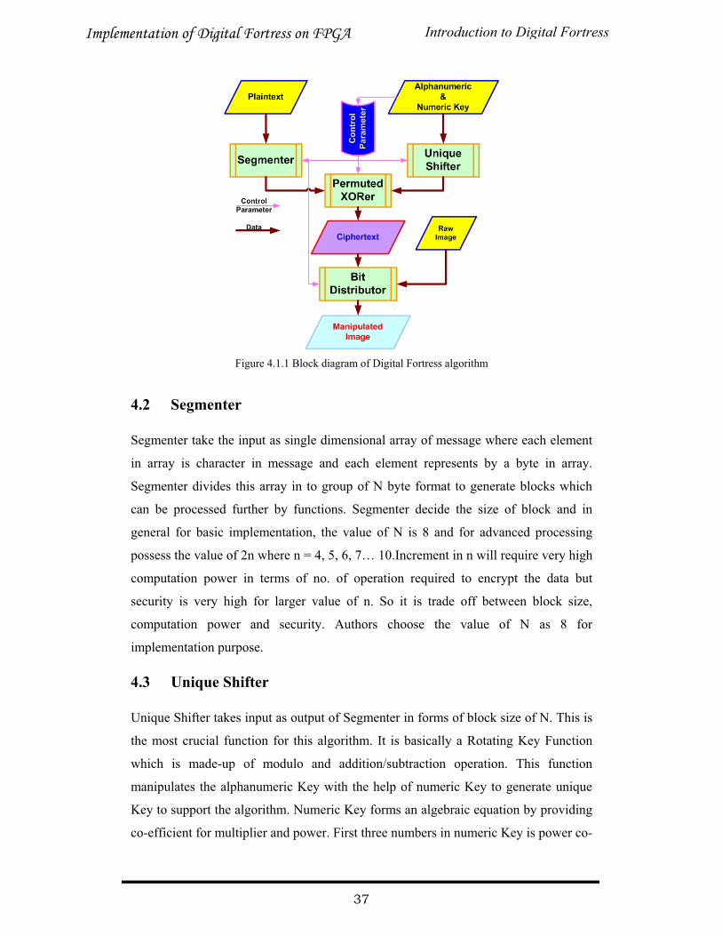
Figure 4.1.1 Block diagram of Digital Fortress algorithm
4.2 Segmenter Segmenter take the input as single dimensional array of message where each element
in array is character in message and each element represents by a byte in array.
Segmenter divides this array in to group of N byte format to generate blocks which
can be processed further by functions. Segmenter decide the size of block and in
general for basic implementation, the value of N is 8 and for advanced processing
possess the value of 2n where n = 4, 5, 6, 7… 10.Increment in n will require very high
computation power in terms of no. of operation required to encrypt the data but
security is very high for larger value of n. So it is trade off between block size,
computation power and security. Authors choose the value of N as 8 for
implementation purpose.
4.3 Unique Shifter Unique Shifter takes input as output of Segmenter in forms of block size of N. This is
the most crucial function for this algorithm. It is basically a Rotating Key Function
which is made-up of modulo and addition/subtraction operation. This function
manipulates the alphanumeric Key with the help of numeric Key to generate unique
Key to support the algorithm. Numeric Key forms an algebraic equation by providing
co-efficient for multiplier and power. First three numbers in numeric Key is power co-
Introduction to Digital FortressImplementation of Digital Fortress on FPGA
37
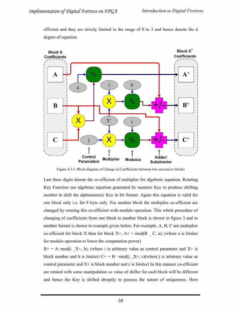
efficient and they are strictly limited in the range of 0 to 3 and hence denote the d
degree of equation.
Figure 4.3.1: Block diagram of Change in Coefficients between two successive blocks
Last three digits denote the co-efficient of multiplier for algebraic equation. Rotating
Key Function use algebraic equation generated by numeric Key to produce shifting
number to shift the alphanumeric Key in bit format. Again this equation is valid for
one block only i.e. for 8 byte only. For another block the multiplier co-efficient are
changed by rotating this co-efficient with modulo operation. This whole procedure of
changing of coefficients from one block to another block is shown in figure 3 and in
another format is shown in example given below. For example, A, B, C are multiplier
co-efficient for block X then for block X+, A+ = mod(B _ C, a); (where a is limiter
for modulo operation to lower the computation power)
B+ = A�mod(i _X+, b); (where i is arbitrary value as control parameter and X+ is
block number and b is limiter) C+ = B �mod(j _X+, c)(where j is arbitrary value as
control parameter and X+ is block number and c is limiter) In this manner co-efficient
are rotated with some manipulation so value of shifter for each block will be different
and hence the Key is shifted abruptly to possess the nature of uniqueness. Here
Introduction to Digital FortressImplementation of Digital Fortress on FPGA
38
alphanumeric Key is shifted bitwise in non-linear manner and dynamic in nature. So
the key is different for the entire symbol range. In this manner unique combination of
Key is generated from finite length and small Key of only 64 bit. This concept
satisfies the theory of Perfect Secrecy along with Vernam’s One Time Padding.
4.4 Permuted XORer This function is made-up of three sub function in which one is primary function and
two are secondary function which support the primary function. Here Modified
XORing is main function along with Rotating Permutation and Rotating Odd Shifter
as secondary functions. Rotating Permutation takes the input as permutation matrix of
8 element sizes and then this matrix is rotated for each block depend up on control
parameters. For Implementation purpose, authors use the linear relation of simple
linear shift in either direction by only one place. This rotation is circular in nature and
by doing so the permutation matrix for 64 elements is generated. If relation is non
linear then permutation is also unique in nature for each block if it satisfies the criteria
of uniqueness. Rotating Odd Shifter is based on the database of finite set of odd
numbers. It takes the input as location number for database and gives the output as
odd number. Here the choice of location number is based on certain relationship
which is the part of control parameters. This relationship is either linear or non-linear
in nature. Authors utilize simple relationship of one increment in location number for
each time function called. Modified XORing is special kind of XORing adopted from
Data Encryption Standard (DES) with certain modification in it. In this first block is
taken and permutation is done with supplied permutation matrix from Rotating
Permutation. After this, data and Key is simply XORed with each other to generate
the intermediate encrypted data. This intermediate encrypted data is divided in to two
equal half each of 4 byte named Right Half and Left Half. According to control
parameter one half is chosen and then this is placed in either as right or left part. After
this remaining part is taken & according to control parameter mirror image of it is
generated. Then this image is XORed with chosen part and placed it as remaining
part. Combination of two parts is final encrypted version or Ciphertext for given
Plaintext and Key.
Introduction to Digital FortressImplementation of Digital Fortress on FPGA
39
4.5 Bit Distributor Bit Distributor is optional part of this algorithm. This function takes the input as
Ciphertext and scrambles it in image according to Bit Distribution function. For this,
function takes the color image having 24 bit pixel and 8 bit each for red, green and
blue plane. For each symbol in Ciphertext a pixel is allotted. Function divides the
symbol in to part of two and three, after this, this part is scrambled in to the lower
nibble of each plane according to parameters. After scrambling the data in to image, it
is impossible to detect the change in picture by human visual system. Integrating all
these function in proper manner this algorithm makes the sense for encryption. This
algorithm needs certain control parameters which can be generated from system itself
and send along with data in scrambled manner.
4.6 Algorithm for Decryption Algorithm for decryption is not as linear as for the symmetric type cryptosystem. First
data is retrieved from image with inverse of BIT DISTRIBUTOR function. Then
Segmenter function is employed to generate proper block size. After this, UNIQUE
SHIFTER function generates unique Key from two Keys. Then inverse PERMUTED
XORER function is employed to generate Plaintext. In decryption, one integrator
function is required to integrate all this function according to control parameters
supplied along with data. This algorithm employs two inverse function, two same
functions and a new function from encryption algorithm. So designing of this is easy
comparing to encryption algorithm when encryption algorithm is available.
4.7 Implementation This pseudo code is employed for implementation purpose. In this block size is taken
as 8 and Rotating Permutation & Rotating Odd Shifter kept linear in fashion. Also bit
distribution function is normal which replace last two or three bit from each byte &
scramble the data in basic format. The notations used in Pseudo Code are given table
4.7.2.1.
4.7.1 Pseudo Code
DIGITAL FORTRESS (p, k1, k2, �P, �, I, Cs)
y � p
Introduction to Digital FortressImplementation of Digital Fortress on FPGA
40
s � S
denote Cs = Hd||Mr||Cr||S||y1||y2||y3||y4||y5
denote y = Mb1||Mb2||Mb3||…||Mbn
denote k1 = a1||a2||a3||a4||a5||a6||a7||a8
denote k2 = x1||x2||x3||x4||x5||x6
P � x1||x2||x3
M � x4||x5||x6
q � 1
for i � 1 to n
{if mod(i,8) = 0 then
{q � q+1
x4 � mod ( * , y1)
x5 � - mod (y2*q, y3)
x6 � + mod (y4*q, y5)
}
x1 � mod (x1, 4)
x2 � mod (x2, 4)
x3 � mod (x3, 4)
n � mod (x4*i^x1+ x5*i^x2+ x6*i^x3 , 64)
denote Mbi = b1||b2||b3||b4||b5||b6||b7||b8
aki � �mod(i,8) (�P (�n (k1) ) )
denote aki = a1||a2||a3||a4||a5||a6||a7||a8
if Hd= 1 then
{
if Mr = 1 then { Li �b8�a8||b7�a7||b6�a6||b5�a5 }
else { Li � b5�a5||b6�a6||b7�a7||b8�a8 }
Ri � b1�a1||b2�a2||b3�a3||b4�a4
if Cr = 1 then { eni = Ri || Ri�Li}
else { eni = Ri�Li || Ri }
}
else
{
if Mr = 1 then { Ri � b4�a4||b3�a3||b2�a2||b1�a1 }
Introduction to Digital FortressImplementation of Digital Fortress on FPGA
41
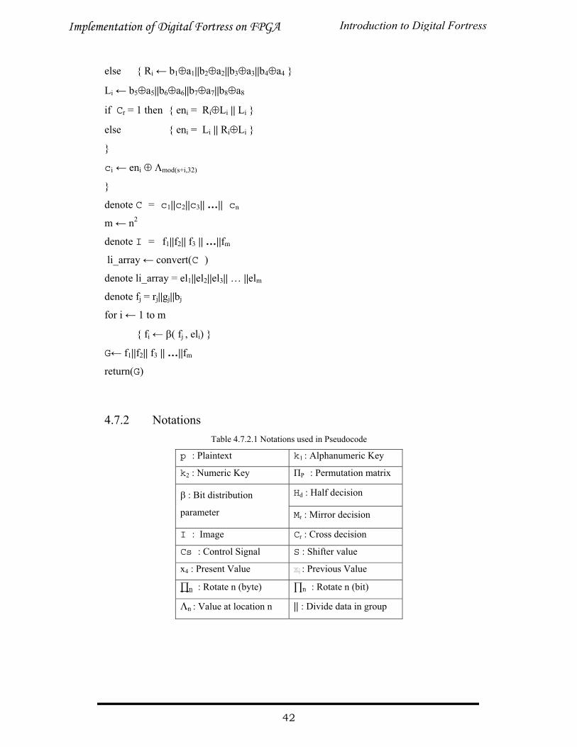
else { Ri � b1�a1||b2�a2||b3�a3||b4�a4 }
Li � b5�a5||b6�a6||b7�a7||b8�a8
if Cr = 1 then { eni = Ri�Li || Li }
else { eni = Li || Ri�Li }
}
ci � eni ���mod(s+i,32)
}
denote C = c1||c2||c3|| …|| cn
m � n2
denote I = f1||f2|| f3 || …||fm
li_array � convert(C )
denote li_array = el1||el2||el3|| … ||elm
denote fj = rj||gj||bj
for i � 1 to m
{ fi � �( fj , eli) }
G� f1||f2|| f3 || …||fm
return(G)
4.7.2 Notations Table 4.7.2.1 Notations used in Pseudocode
p : Plaintext k1 : Alphanumeric Key
k2 : Numeric Key �P : Permutation matrix
Hd : Half decision � : Bit distribution
parameter Mr : Mirror decision
I : Image Cr : Cross decision
Cs : Control Signal S : Shifter value
x4 : Present Value : Previous Value
�n : Rotate n (byte) �n : Rotate n (bit)
�n : Value at location n || : Divide data in group
Introduction to Digital FortressImplementation of Digital Fortress on FPGA
42
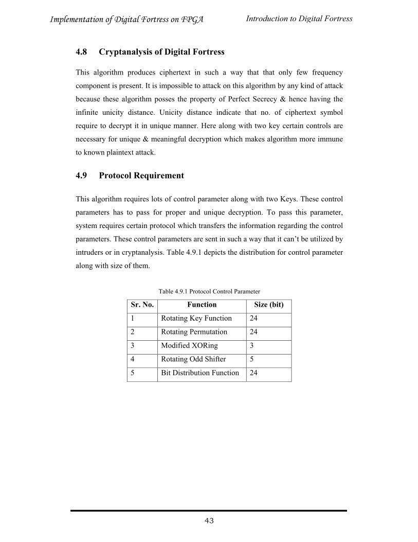
4.8 Cryptanalysis of Digital Fortress This algorithm produces ciphertext in such a way that that only few frequency
component is present. It is impossible to attack on this algorithm by any kind of attack
because these algorithm posses the property of Perfect Secrecy & hence having the
infinite unicity distance. Unicity distance indicate that no. of ciphertext symbol
require to decrypt it in unique manner. Here along with two key certain controls are
necessary for unique & meaningful decryption which makes algorithm more immune
to known plaintext attack.
4.9 Protocol Requirement
This algorithm requires lots of control parameter along with two Keys. These control
parameters has to pass for proper and unique decryption. To pass this parameter,
system requires certain protocol which transfers the information regarding the control
parameters. These control parameters are sent in such a way that it can’t be utilized by
intruders or in cryptanalysis. Table 4.9.1 depicts the distribution for control parameter
along with size of them.
Table 4.9.1 Protocol Control Parameter
Sr. No. Function Size (bit)
1 Rotating Key Function 24
2 Rotating Permutation 24
3 Modified XORing 3
4 Rotating Odd Shifter 5
5 Bit Distribution Function 24
Introduction to Digital FortressImplementation of Digital Fortress on FPGA
43
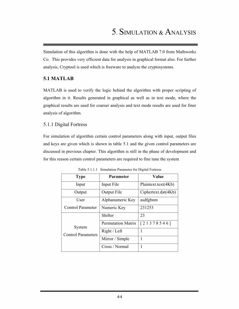
5. SIMULATION & ANALYSIS
Simulation of this algorithm is done with the help of MATLAB 7.0 from Mathworks
Co. This provides very efficient data for analysis in graphical format also. For further
analysis, Cryptool is used which is freeware to analyze the cryptosystems.
5.1 MATLAB
MATLAB is used to verify the logic behind the algorithm with proper scripting of
algorithm in it. Results generated in graphical as well as in text mode, where the
graphical results are used for coarser analysis and text mode results are used for finer
analysis of algorithm.
5.1.1 Digital Fortress
For simulation of algorithm certain control parameters along with input, output files
and keys are given which is shown in table 5.1 and the given control parameters are
discussed in previous chapter. This algorithm is still in the phase of development and
for this reason certain control parameters are required to fine tune the system
Table 5.1.1.1 Simulation Parameter for Digital Fortress
Type Parameter Value
Input Input File Plaintext.text(4Kb)
Output Output File Ciphertext.dat(4Kb)
Alphanumeric Key asdfgbnm User
Control Parameter Numeric Key 231253
Shifter 23
Permutation Matrix [ 2 1 3 7 8 5 4 6 ]
Right / Left 1
Mirror / Simple 1
System
Control Parameters
Cross / Normal 1
44
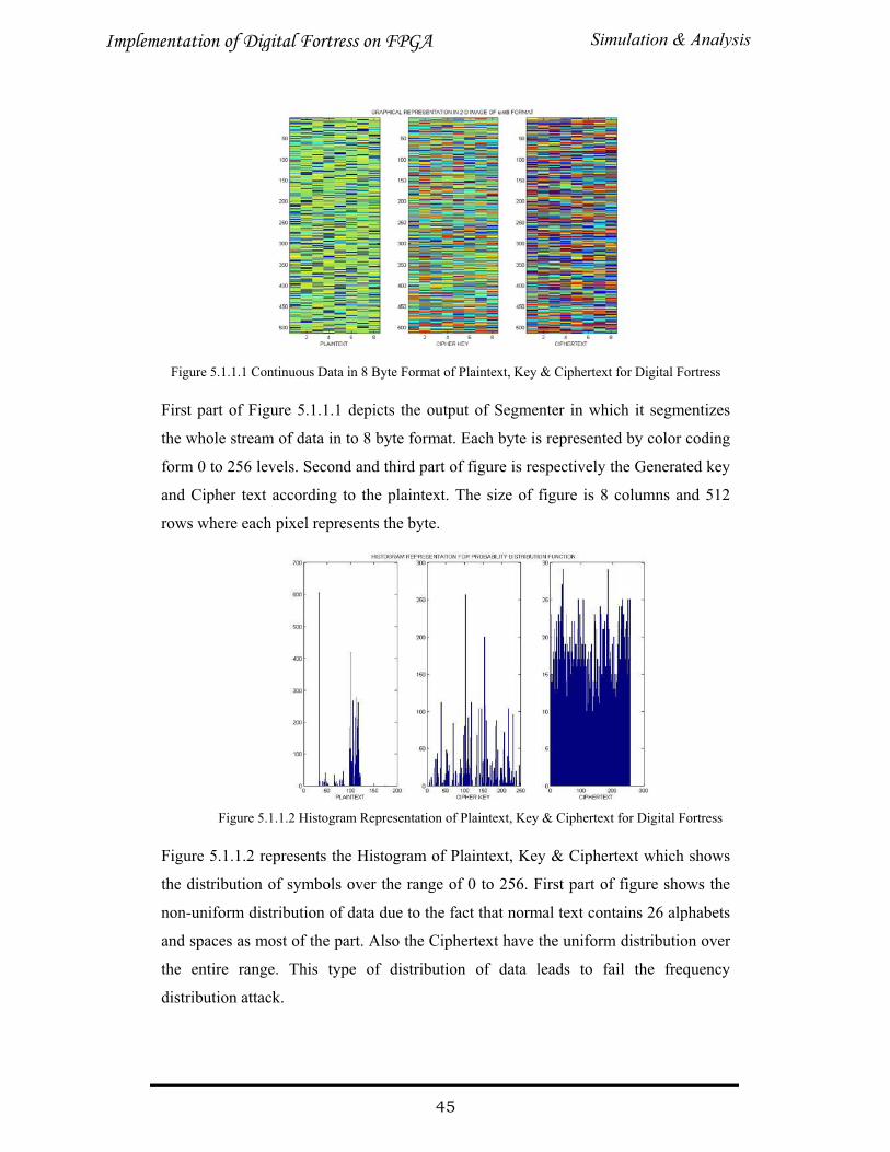
Figure 5.1.1.1 Continuous Data in 8 Byte Format of Plaintext, Key & Ciphertext for Digital Fortress
First part of Figure 5.1.1.1 depicts the output of Segmenter in which it segmentizes
the whole stream of data in to 8 byte format. Each byte is represented by color coding
form 0 to 256 levels. Second and third part of figure is respectively the Generated key
and Cipher text according to the plaintext. The size of figure is 8 columns and 512
rows where each pixel represents the byte.
Figure 5.1.1.2 Histogram Representation of Plaintext, Key & Ciphertext for Digital Fortress
Figure 5.1.1.2 represents the Histogram of Plaintext, Key & Ciphertext which shows
the distribution of symbols over the range of 0 to 256. First part of figure shows the
non-uniform distribution of data due to the fact that normal text contains 26 alphabets
and spaces as most of the part. Also the Ciphertext have the uniform distribution over
the entire range. This type of distribution of data leads to fail the frequency
distribution attack.
Simulation & AnalysisImplementation of Digital Fortress on FPGA
45
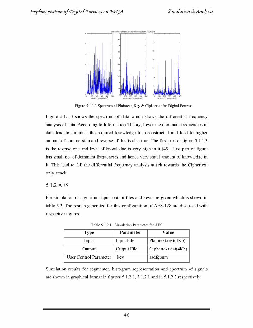
Figure 5.1.1.3 Spectrum of Plaintext, Key & Ciphertext for Digital Fortress
Figure 5.1.1.3 shows the spectrum of data which shows the differential frequency
analysis of data. According to Information Theory, lower the dominant frequencies in
data lead to diminish the required knowledge to reconstruct it and lead to higher
amount of compression and reverse of this is also true. The first part of figure 5.1.1.3
is the reverse one and level of knowledge is very high in it [45]. Last part of figure
has small no. of dominant frequencies and hence very small amount of knowledge in
it. This lead to fail the differential frequency analysis attack towards the Ciphertext
only attack.
5.1.2 AES
For simulation of algorithm input, output files and keys are given which is shown in
table 5.2. The results generated for this configuration of AES-128 are discussed with
respective figures.
Table 5.1.2.1 Simulation Parameter for AES
Type Parameter Value
Input Input File Plaintext.text(4Kb)
Output Output File Ciphertext.dat(4Kb)
User Control Parameter key asdfgbnm
Simulation results for segmenter, histogram representation and spectrum of signals
are shown in graphical format in figures 5.1.2.1, 5.1.2.1 and in 5.1.2.3 respectively.
Simulation & AnalysisImplementation of Digital Fortress on FPGA
46
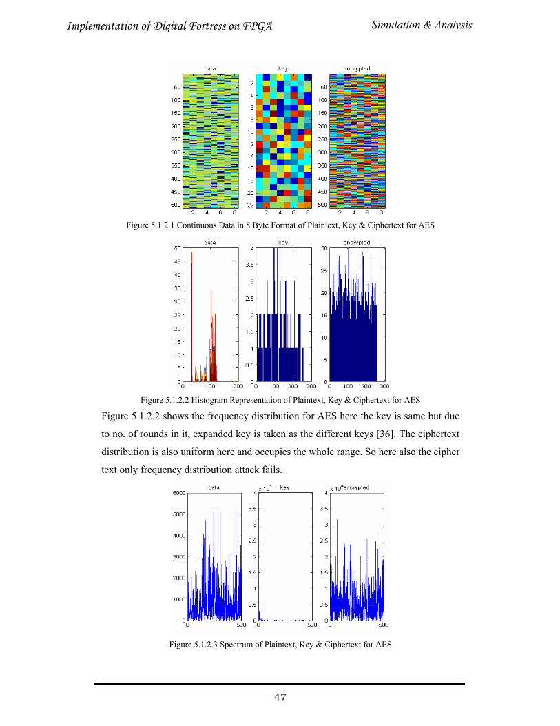
Figure 5.1.2.1 Continuous Data in 8 Byte Format of Plaintext, Key & Ciphertext for AES
Figure 5.1.2.2 Histogram Representation of Plaintext, Key & Ciphertext for AES
Figure 5.1.2.2 shows the frequency distribution for AES here the key is same but due
to no. of rounds in it, expanded key is taken as the different keys [36]. The ciphertext
distribution is also uniform here and occupies the whole range. So here also the cipher
text only frequency distribution attack fails.
Figure 5.1.2.3 Spectrum of Plaintext, Key & Ciphertext for AES
Simulation & AnalysisImplementation of Digital Fortress on FPGA
47
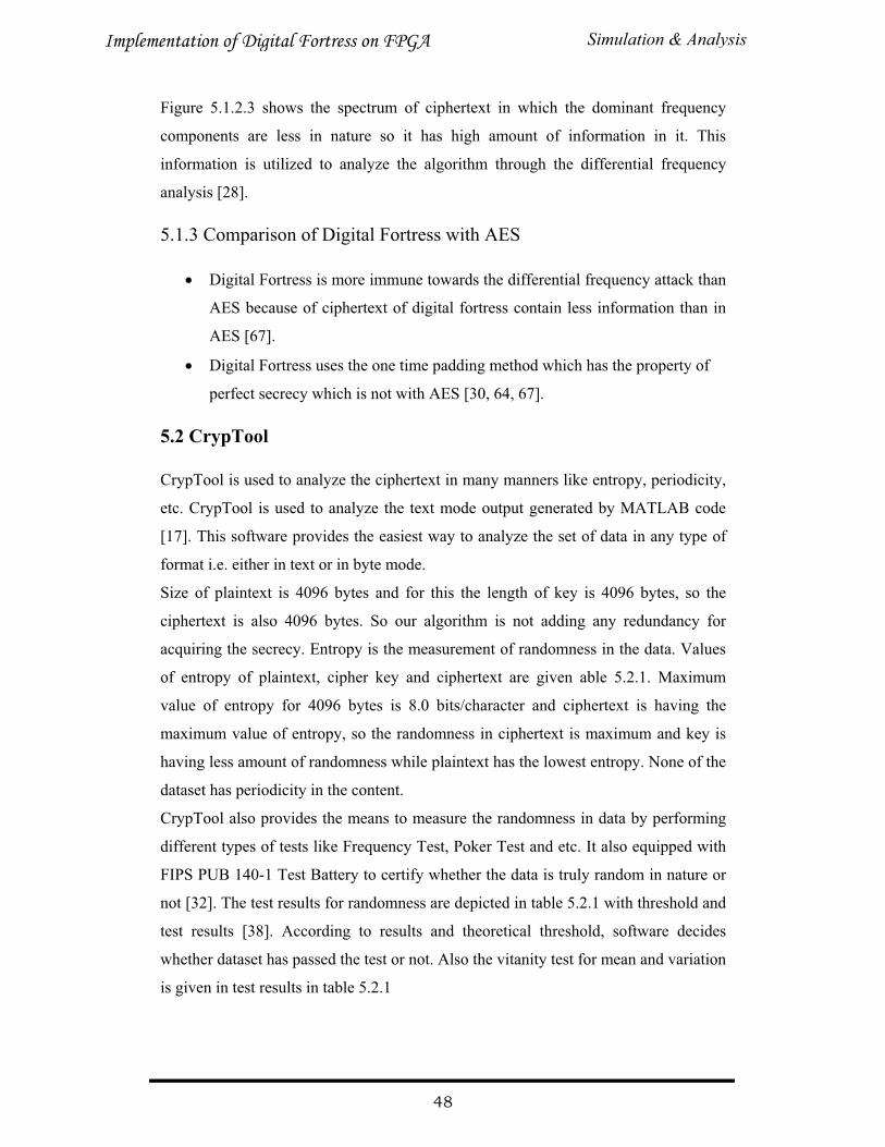
Figure 5.1.2.3 shows the spectrum of ciphertext in which the dominant frequency
components are less in nature so it has high amount of information in it. This
information is utilized to analyze the algorithm through the differential frequency
analysis [28].
5.1.3 Comparison of Digital Fortress with AES
� Digital Fortress is more immune towards the differential frequency attack than
AES because of ciphertext of digital fortress contain less information than in
AES [67].
� Digital Fortress uses the one time padding method which has the property of
perfect secrecy which is not with AES [30, 64, 67].
5.2 CrypTool
CrypTool is used to analyze the ciphertext in many manners like entropy, periodicity,
etc. CrypTool is used to analyze the text mode output generated by MATLAB code
[17]. This software provides the easiest way to analyze the set of data in any type of
format i.e. either in text or in byte mode.
Size of plaintext is 4096 bytes and for this the length of key is 4096 bytes, so the
ciphertext is also 4096 bytes. So our algorithm is not adding any redundancy for
acquiring the secrecy. Entropy is the measurement of randomness in the data. Values
of entropy of plaintext, cipher key and ciphertext are given able 5.2.1. Maximum
value of entropy for 4096 bytes is 8.0 bits/character and ciphertext is having the
maximum value of entropy, so the randomness in ciphertext is maximum and key is
having less amount of randomness while plaintext has the lowest entropy. None of the
dataset has periodicity in the content.
CrypTool also provides the means to measure the randomness in data by performing
different types of tests like Frequency Test, Poker Test and etc. It also equipped with
FIPS PUB 140-1 Test Battery to certify whether the data is truly random in nature or
not [32]. The test results for randomness are depicted in table 5.2.1 with threshold and
test results [38]. According to results and theoretical threshold, software decides
whether dataset has passed the test or not. Also the vitanity test for mean and variation
is given in test results in table 5.2.1
Simulation & AnalysisImplementation of Digital Fortress on FPGA
48
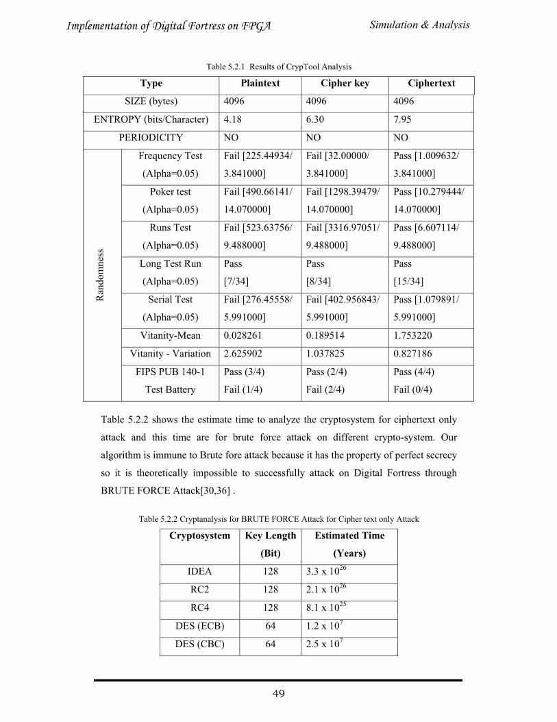
Table 5.2.1 Results of CrypTool Analysis
Type Plaintext Cipher key Ciphertext
SIZE (bytes) 4096 4096 4096
ENTROPY (bits/Character) 4.18 6.30 7.95
PERIODICITY NO NO NO
Frequency Test
(Alpha=0.05)
Fail [225.44934/
3.841000]
Fail [32.00000/
3.841000]
Pass [1.009632/
3.841000]
Poker test
(Alpha=0.05)
Fail [490.66141/
14.070000]
Fail [1298.39479/
14.070000]
Pass [10.279444/
14.070000]
Runs Test
(Alpha=0.05)
Fail [523.63756/
9.488000]
Fail [3316.97051/
9.488000]
Pass [6.607114/
9.488000]
Long Test Run
(Alpha=0.05)
Pass
[7/34]
Pass
[8/34]
Pass
[15/34]
Serial Test
(Alpha=0.05)
Fail [276.45558/
5.991000]
Fail [402.956843/
5.991000]
Pass [1.079891/
5.991000]
Vitanity-Mean 0.028261 0.189514 1.753220
Vitanity - Variation 2.625902 1.037825 0.827186
Ran
dom
ness
FIPS PUB 140-1
Test Battery
Pass (3/4)
Fail (1/4)
Pass (2/4)
Fail (2/4)
Pass (4/4)
Fail (0/4)
Table 5.2.2 shows the estimate time to analyze the cryptosystem for ciphertext only
attack and this time are for brute force attack on different crypto-system. Our
algorithm is immune to Brute fore attack because it has the property of perfect secrecy
so it is theoretically impossible to successfully attack on Digital Fortress through
BRUTE FORCE Attack[30,36] .
Table 5.2.2 Cryptanalysis for BRUTE FORCE Attack for Cipher text only Attack
Cryptosystem Key Length
(Bit)
Estimated Time
(Years)
IDEA 128 3.3 x 1026
RC2 128 2.1 x 1026
RC4 128 8.1 x 1025
DES (ECB) 64 1.2 x 10⁷
DES (CBC) 64 2.5 x 10⁷
Simulation & AnalysisImplementation of Digital Fortress on FPGA
49
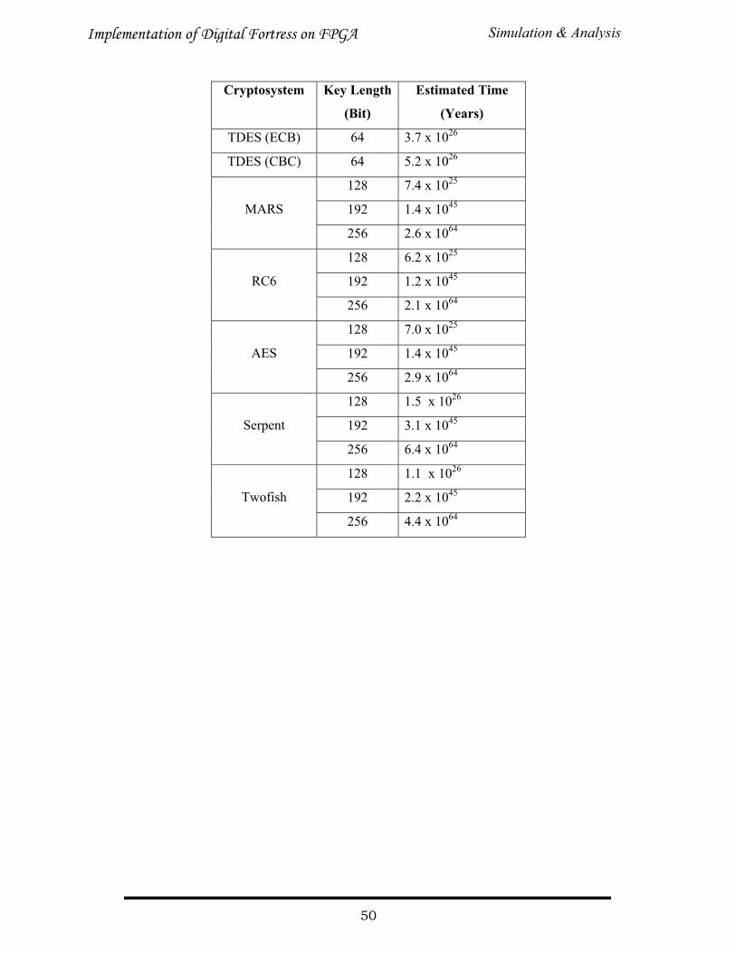
Cryptosystem Key Length
(Bit)
Estimated Time
(Years)
TDES (ECB) 64 3.7 x 1026
TDES (CBC) 64 5.2 x 1026
128 7.4 x 1025
192 1.4 x 1045MARS
256 2.6 x 1064
128 6.2 x 1025
192 1.2 x 1045RC6
256 2.1 x 1064
128 7.0 x 1025
192 1.4 x 1045AES
256 2.9 x 1064
128 1.5 x 1026
192 3.1 x 1045Serpent
256 6.4 x 1064
128 1.1 x 1026
192 2.2 x 1045Twofish
256 4.4 x 1064
Simulation & AnalysisImplementation of Digital Fortress on FPGA
50
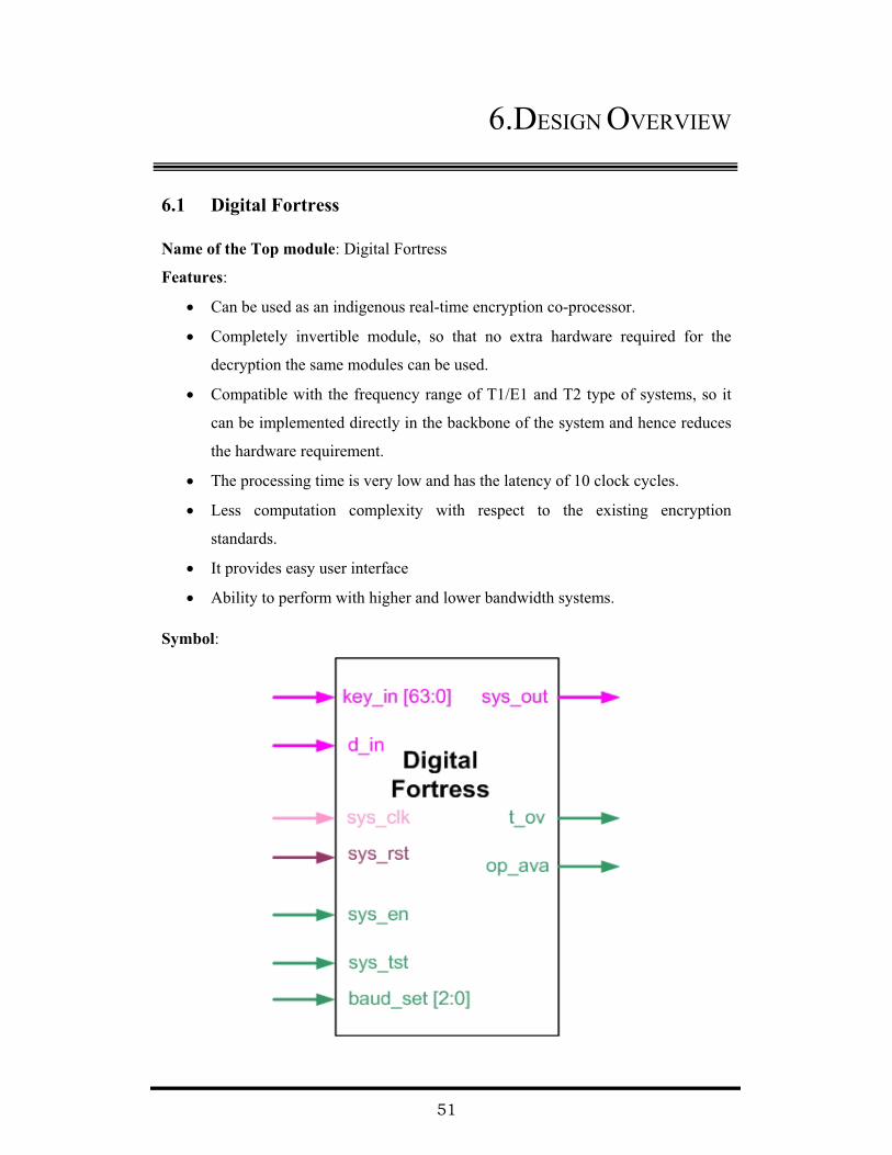
6.DESIGN OVERVIEW
6.1 Digital Fortress
Name of the Top module: Digital Fortress
Features:
� Can be used as an indigenous real-time encryption co-processor.
� Completely invertible module, so that no extra hardware required for the
decryption the same modules can be used.
� Compatible with the frequency range of T1/E1 and T2 type of systems, so it
can be implemented directly in the backbone of the system and hence reduces
the hardware requirement.
� The processing time is very low and has the latency of 10 clock cycles.
� Less computation complexity with respect to the existing encryption
standards.
� It provides easy user interface
� Ability to perform with higher and lower bandwidth systems.
Symbol:
51
Methodology and Design:
Modeling:
Model the proposed encryption standard using mathematical model as well as
behavioral & functional model & make it compatible with existing standards.
Construction /experiments / programming:
Check & analyze the different parameters of existing network to tune our standard
according to it. We will do programming in two different languages for particular
reasons. We use MATLAB to check the validity of algorithm, and to understand
algorithm conceptually in terms of existing protocol stack & VHDL for hardware
realization of the protocol.
Testing and Verification:
Testing is done by creating a test bench to generate different test vectors and also to
check the outcome of each and every test vector. The verification is performed by
cross checking and comparing the VHDL outcomes with the out puts we are getting
on MATLAB and with the standard parameters of cryptography.
System integration:
The module is interfaced with the computer to take the input as a stream of bits
(irrespective of being an image or data) through the serial port. The processed data
from the FPGA prototype is sent back to the same machine using a simple software
interface.
PIN Description:
Name Type Description
sys_clk Input Global system clock
sys_rst Input Global system reset
sys_tst Input System test to test the system with its default settings
sys_en Input System enable pin to enable the system for further processing
key_in Input To provide the alphanumeric key as an input
din Input Data input in serial mode
baud_set Input Baud rate set, An input pin to adjust the baud rates of the system
baud rate that is compatible with the external system.
op_ava Output Output available indicator of the availability of the output
Design OverviewImplementation of Digital Fortress on FPGA
52
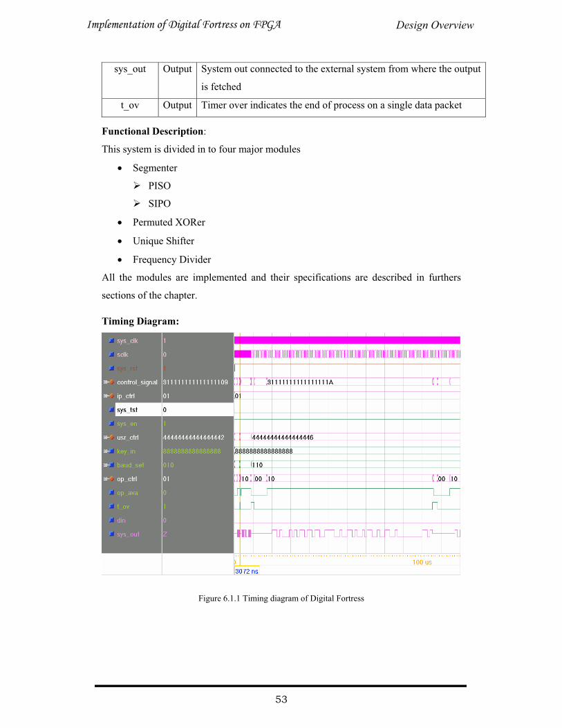
sys_out Output System out connected to the external system from where the output
is fetched
t_ov Output Timer over indicates the end of process on a single data packet
Functional Description:
This system is divided in to four major modules
� Segmenter
� PISO
� SIPO
� Permuted XORer
� Unique Shifter
� Frequency Divider
All the modules are implemented and their specifications are described in furthers
sections of the chapter.
Timing Diagram:
Figure 6.1.1 Timing diagram of Digital Fortress
Design OverviewImplementation of Digital Fortress on FPGA
53

Functional Block Diagram:
Figure 6.1.2 Block Diagram of Digital Fortress
Design OverviewImplementation of Digital Fortress on FPGA
54
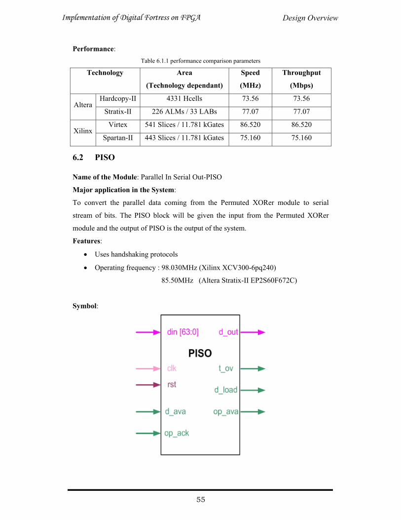
Performance:Table 6.1.1 performance comparison parameters
Technology Area
(Technology dependant)
Speed
(MHz)
Throughput
(Mbps)
Hardcopy-II 4331 Hcells 73.56 73.56Altera
Stratix-II 226 ALMs / 33 LABs 77.07 77.07
Virtex 541 Slices / 11.781 kGates 86.520 86.520Xilinx
Spartan-II 443 Slices / 11.781 kGates 75.160 75.160
6.2 PISO
Name of the Module: Parallel In Serial Out-PISO
Major application in the System:
To convert the parallel data coming from the Permuted XORer module to serial
stream of bits. The PISO block will be given the input from the Permuted XORer
module and the output of PISO is the output of the system.
Features:
� Uses handshaking protocols
� Operating frequency : 98.030MHz (Xilinx XCV300-6pq240)
85.50MHz (Altera Stratix-II EP2S60F672C)
Symbol:
Design OverviewImplementation of Digital Fortress on FPGA
55
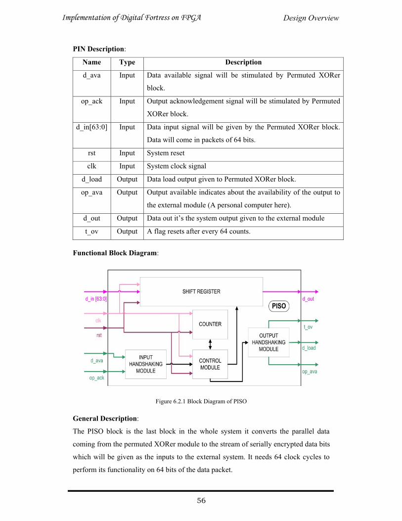
PIN Description:
Name Type Description
d_ava Input Data available signal will be stimulated by Permuted XORer
block.
op_ack Input Output acknowledgement signal will be stimulated by Permuted
XORer block.
d_in[63:0] Input Data input signal will be given by the Permuted XORer block.
Data will come in packets of 64 bits.
rst Input System reset
clk Input System clock signal
d_load Output Data load output given to Permuted XORer block.
op_ava Output Output available indicates about the availability of the output to
the external module (A personal computer here).
d_out Output Data out it’s the system output given to the external module
t_ov Output A flag resets after every 64 counts.
Functional Block Diagram:
Figure 6.2.1 Block Diagram of PISO
General Description:
The PISO block is the last block in the whole system it converts the parallel data
coming from the permuted XORer module to the stream of serially encrypted data bits
which will be given as the inputs to the external system. It needs 64 clock cycles to
perform its functionality on 64 bits of the data packet.
Design OverviewImplementation of Digital Fortress on FPGA
56
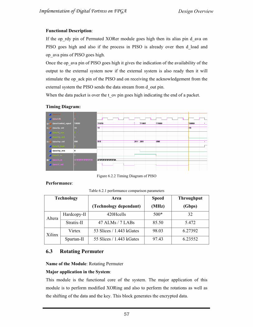
Functional Description:
If the op_rdy pin of Permuted XORer module goes high then its alias pin d_ava on
PISO goes high and also if the process in PISO is already over then d_load and
op_ava pins of PISO goes high.
Once the op_ava pin of PISO goes high it gives the indication of the availability of the
output to the external system now if the external system is also ready then it will
stimulate the op_ack pin of the PISO and on receiving the acknowledgement from the
external system the PISO sends the data stream from d_out pin.
When the data packet is over the t_ov pin goes high indicating the end of a packet.
Timing Diagram:
Figure 6.2.2 Timing Diagram of PISO
Performance:Table 6.2.1 performance comparison parameters
Technology Area
(Technology dependant)
Speed
(MHz)
Throughput
(Gbps)
Hardcopy-II 420Hcells 500* 32Altera
Stratix-II 47 ALMs / 7 LABs 85.50 5.472
Virtex 53 Slices / 1.443 kGates 98.03 6.27392Xilinx
Spartan-II 55 Slices / 1.443 kGates 97.43 6.23552
6.3 Rotating Permuter
Name of the Module: Rotating Permuter
Major application in the System:
This module is the functional core of the system. The major application of this
module is to perform modified XORing and also to perform the rotations as well as
the shifting of the data and the key. This block generates the encrypted data.
Design OverviewImplementation of Digital Fortress on FPGA
57

Features:
� The Brain of the system
� Uses the modified XORing logic to obtain the characteristic of Randomization
� Uses handshaking protocols
� Operating frequency : 202.634MHz(Xilinx XCV300-6pq240)
� 500MHz (Altera Stratix-II EP2S60F672C)
Symbol:
PIN Description:
Name Type Description
da[7:0][7:0] Input Data in coming from the SIPO module in the form of packets
of 8 bits.
key[7:0][7:0
]
Input Rotated alphanumeric key coming from the Unique Shifter
module in the form of packets of 8 bits.
clk Input System clock signal
H_RL Input Half Decision provided by the user to decide on which half of
the key to be operated upon.
Design OverviewImplementation of Digital Fortress on FPGA
58
N_C Input Normal/Cross provided by the user to decide the operation to
be performed in a normal pattern or cross pattern.
S_R Input Simple Mirror provided by the user to determine the operation
to be performed on the key as it is or after inverting it by 180.
d_en Input Data enable provided from the SIPO module
op_ack Input Output acknowledgement provided from the output of the PISO
module
op[7:0][7:0] Output XORed Output will be given to the input of the PISO block
m_ack Output Acknowledgement given to SIPO and Unique Shifter Modules
for synchronization.
m_en Output To provide the enable signal to unique shifter
op_rdy Output Output ready is for providing the stimulation to the PISO block
General Description:
Rotating Permuter or permuted XORer module is the heart of the Digital Fortress as it
takes the alphanumeric key and data from the SIPO and the Unique Shifter modules
respectively.
This function is made-up of three sub functions out of which one is primary function
and two are secondary functions which support the primary function. Here Modified
XORing is the main function along with Rotating Permutation and Rotating Odd
Shifter as secondary functions. Rotating Permutation takes the input as permutation
matrix of 8 element sizes and then this matrix is rotated for each block depend up on
control parameters. For implementation purpose, authors have used the linear relation
of simple linear shift in either direction by only one place. This rotation is circular in
nature and by doing so the permutation matrix for 64 elements is generated. If relation
is non linear then permutation is also unique in nature for each block if it satisfies the
criteria of uniqueness. Rotating Odd Shifter is based on the database of finite set of
odd numbers. It takes the input as location number for database and gives the output
as odd number. Here the choice of location number is based on certain relationship
which is the part of control parameters. This relationship is either linear or non-linear
in nature. Firstly a data block is taken and permutation is done with supplied
permutation matrix from Rotating Permutation. After this, data and Key is simply
XORed with each other to generate the intermediate encrypted data. This intermediate
encrypted data is divided in to two equal half each of 4 byte named Right Half and
Design OverviewImplementation of Digital Fortress on FPGA
59
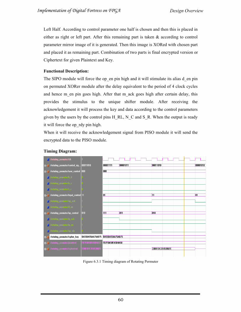
Left Half. According to control parameter one half is chosen and then this is placed in
either as right or left part. After this remaining part is taken & according to control
parameter mirror image of it is generated. Then this image is XORed with chosen part
and placed it as remaining part. Combination of two parts is final encrypted version or
Ciphertext for given Plaintext and Key.
Functional Description:
The SIPO module will force the op_en pin high and it will stimulate its alias d_en pin
on permuted XORer module after the delay equivalent to the period of 4 clock cycles
and hence m_en pin goes high. After that m_ack goes high after certain delay, this
provides the stimulus to the unique shifter module. After receiving the
acknowledgement it will process the key and data according to the control parameters
given by the users by the control pins H_RL, N_C and S_R. When the output is ready
it will force the op_rdy pin high.
When it will receive the acknowledgement signal from PISO module it will send the
encrypted data to the PISO module.
Timing Diagram:
Figure 6.3.1 Timing diagram of Rotating Permuter
Design OverviewImplementation of Digital Fortress on FPGA
60
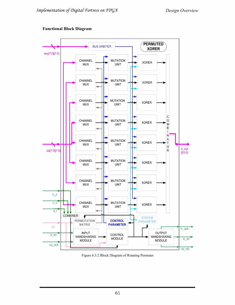
Functional Block Diagram
Figure 6.3.2 Block Diagram of Rotating Permuter
Design OverviewImplementation of Digital Fortress on FPGA
61
Performance:Table 6.3.1 performance comparison parameters
Technology Area
(Technology dependant)
Speed
(MHz)
Throughput
(Gbps)
Hardcopy-II 234Hcells 500* 32Altera
Stratix-II 47 ALMs / 7 LABs 500* 32
Virtex 357 Slices / 4.604 kGates 202.634 12.968Xilinx
Spartan-II 355 Slices / 4.595 kGates 323.520 20.705
6.4 SIPO
Name of the Module: Serial In Parallel Out-SIPO
Major application in the System:
To convert the stream of the data coming serially from the external system to the data
packets of 64 bits. So that the speed of the system can be increased.
Features:
� Synchronization at higher frequency of operation
� Uses handshaking protocols
� Operating frequency : 98.030MHz (Xilinx XCV300-6pq240)
83.08MHz (Altera Stratix-II EP2S60F672C)
Symbol:
Design OverviewImplementation of Digital Fortress on FPGA
62
PIN Description:
Name Type Description
d_req Input Data Request is to be sent by the external system (A personal
computer here).
d_en Input Data enable provided by the external system after the SIPO
modules provides the acknowledgement.
op_ack Input Output a acknowledgement given by the Unique Shifter and the
Permuted XORer modules
clk Input System clock signal
rst Input System reset
d_in Input Data Input given serially by the user or the external system
d_ack Output Acknowledgement given by the SIPO module to the external
system indicating the system is ready to accept the data.
op_en Output Output enable is given as the input to the permuted XORer.
e_clk Output Enable clock for the synchronization with another system or
block
d_out[63:0] Output Data out will be given to the permuted XORer module in the
form of the packets of 64 bits.
General Description:
The SIPO block is a part of the SEGMENTER module and it is used for the serial to
parallel conversion of the data. It is the first and the foremost block which actually
communicates with the external device. The output will be in terms of the data
packets of 64 bits.
Functional Description:
The external module requests SIPO module by enforcing the d_req pin high. If the
SIPO module is ready it will give the acknowledgement by enabling the d-ack pin,
once the external module receives the acknowledgement it will send enabling signal
to the SIPO module by stimulating the d_en pin after that the SIPO will receive the
data stream. After 64 clock cycles the op_en pin goes high and after that the permuted
XORer will provide the acknowledgement by providing the logic ‘1’ at op_ack pin.
Soon after that the data will be transferred to the permuted XORer module and it will
be in the form of the packets of 64 bits.
Design OverviewImplementation of Digital Fortress on FPGA
63

Block Diagram:
Figure 6.4.1 Block Diagram of SIPO
Timing Diagram:
Figure 6.4.2 Timing diagram of SIPO
Performance:Table 6.4.1 performance comparison parameters
Technology Area
(Technology dependant)
Speed
(MHz)
Throughput
(Mbps)
Hardcopy-II 3114Hcells 400* 400*Altera
Stratix-II 196 ALMs / 48 LABs 83.08 83.08
Virtex 142 Slices / 2.108 kGates 98.030 98.030Xilinx
Spartan-II 142 Slices / 2.108 kGates 97.428 97.428
Design OverviewImplementation of Digital Fortress on FPGA
64
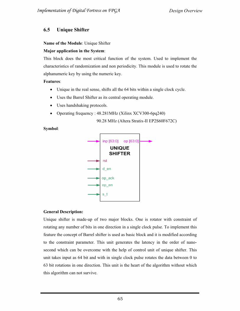
6.5 Unique Shifter
Name of the Module: Unique Shifter
Major application in the System:
This block does the most critical function of the system. Used to implement the
characteristics of randomization and non periodicity. This module is used to rotate the
alphanumeric key by using the numeric key.
Features:
� Unique in the real sense, shifts all the 64 bits within a single clock cycle.
� Uses the Barrel Shifter as its central operating module.
� Uses handshaking protocols.
� Operating frequency : 48.281MHz (Xilinx XCV300-6pq240)
90.28 MHz (Altera Stratix-II EP2S60F672C)
Symbol:
General Description:
Unique shifter is made-up of two major blocks. One is rotator with constraint of
rotating any number of bits in one direction in a single clock pulse. To implement this
feature the concept of Barrel shifter is used as basic block and it is modified according
to the constraint parameter. This unit generates the latency in the order of nano-
second which can be overcome with the help of control unit of unique shifter. This
unit takes input as 64 bit and with in single clock pulse rotates the data between 0 to
63 bit rotations in one direction. This unit is the heart of the algorithm without which
this algorithm can not survive.
Design OverviewImplementation of Digital Fortress on FPGA
65
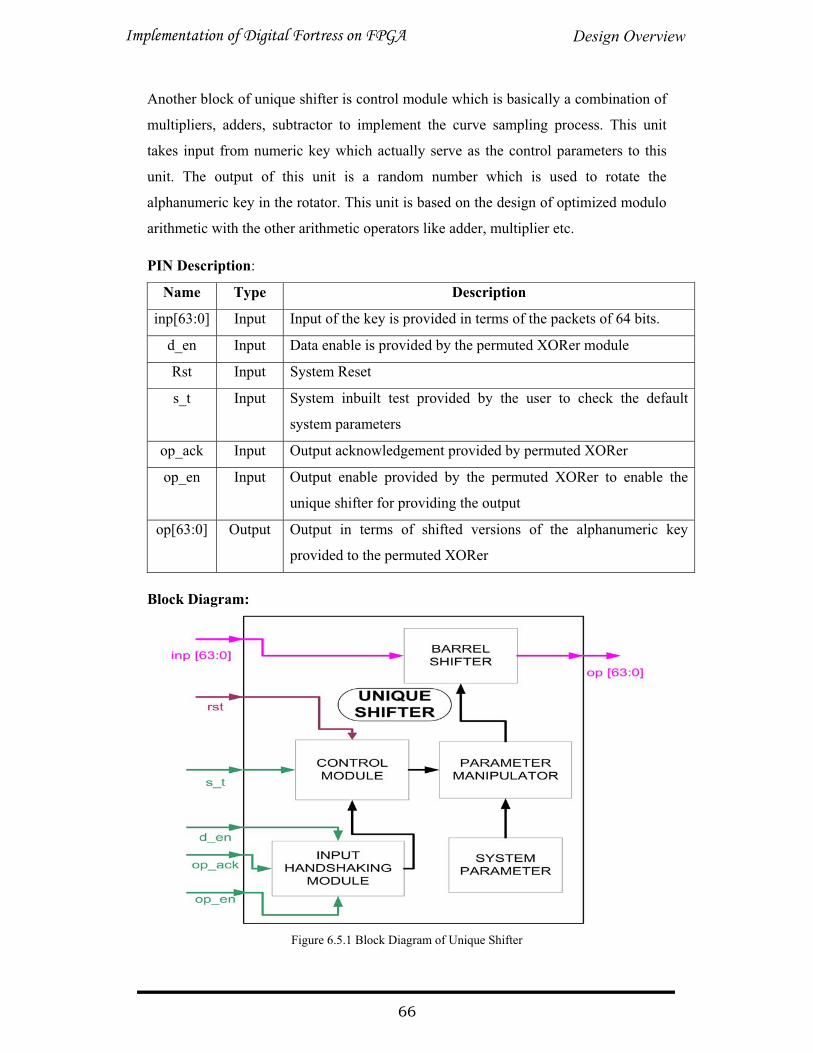
Another block of unique shifter is control module which is basically a combination of
multipliers, adders, subtractor to implement the curve sampling process. This unit
takes input from numeric key which actually serve as the control parameters to this
unit. The output of this unit is a random number which is used to rotate the
alphanumeric key in the rotator. This unit is based on the design of optimized modulo
arithmetic with the other arithmetic operators like adder, multiplier etc.
PIN Description:
Name Type Description
inp[63:0] Input Input of the key is provided in terms of the packets of 64 bits.
d_en Input Data enable is provided by the permuted XORer module
Rst Input System Reset
s_t Input System inbuilt test provided by the user to check the default
system parameters
op_ack Input Output acknowledgement provided by permuted XORer
op_en Input Output enable provided by the permuted XORer to enable the
unique shifter for providing the output
op[63:0] Output Output in terms of shifted versions of the alphanumeric key
provided to the permuted XORer
Block Diagram:
Figure 6.5.1 Block Diagram of Unique Shifter
Design OverviewImplementation of Digital Fortress on FPGA
66

Functional Description:
The d_en pin will be stimulated by the SIPO module and the op_en pin of Unique
Shifter module with the delay of 4 clock pulses after that Unique Shifter module will
process the key and when the permuted XORer forces the m_ack pin high then its
alias pin op_ack on Unique Shifter will be stimulated and after that it will transfers
the processed key to the permuted XORer.
Timing Diagram:
Figure 6.5.2 Timing diagram of Unique Shifter
Performance:Table 6.5.1 performance comparison parameters
Technology Area
(Technology dependant)
Speed
(MHz)
Throughput
(Gbps)
Hardcopy-II 3649Hcells 122.80 7.895Altera
Stratix-II 212 ALMs / 3 DSP Blocks 90.28 5.777
Virtex 117 Slices / 5.733 kGates 48.281 3.089Xilinx
Spartan-II 117Slices /5.733 kGates 49.065 3.140
6.6 Frequency Divider
Name of the Module: Frequency Divisor
Major application in the System:
The major area of applications is to provide multiple choices of Baud rates. For
communicating with the external systems.
Features:
� An indigenous block to provide multiple baud rates, as listed in the table 6.6.1.
� Operating frequency : 175.162 MHz (Xilinx XCV300-6pq240)
� 500 MHz (Altera Stratix-II EP2S60F672C)
Design OverviewImplementation of Digital Fortress on FPGA
67
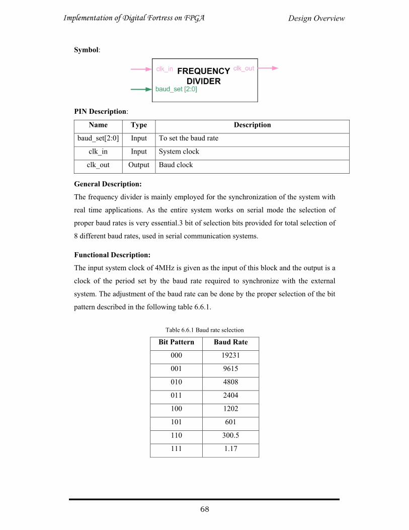
Symbol:
PIN Description:
Name Type Description
baud_set[2:0] Input To set the baud rate
clk_in Input System clock
clk_out Output Baud clock
General Description:
The frequency divider is mainly employed for the synchronization of the system with
real time applications. As the entire system works on serial mode the selection of
proper baud rates is very essential.3 bit of selection bits provided for total selection of
8 different baud rates, used in serial communication systems.
Functional Description:
The input system clock of 4MHz is given as the input of this block and the output is a
clock of the period set by the baud rate required to synchronize with the external
system. The adjustment of the baud rate can be done by the proper selection of the bit
pattern described in the following table 6.6.1.
Table 6.6.1 Baud rate selection
Bit Pattern Baud Rate
000 19231
001 9615
010 4808
011 2404
100 1202
101 601
110 300.5
111 1.17
Design OverviewImplementation of Digital Fortress on FPGA
68

Functional Block Diagram:
Figure 6.6.1 Block Diagram of Frequency Divider
Timing Diagram:
Figure 6.6.2 Timing diagram of Frequency Divider
Performance:Table 6.6.2 performance comparison parameters
Technology Area
(Technology dependant)
Speed
(MHz)
Throughput
(Mbps)
Hardcopy-II 188Hcells 331.670 331.670Altera
Stratix-II 14 ALMs / 3 LABs 500* 500*
Virtex 22 Slices / 359 kGates 175.162 175.162Xilinx
Spartan-II 22 Slices / 359 kGates 172.771 172.771
Design OverviewImplementation of Digital Fortress on FPGA
69
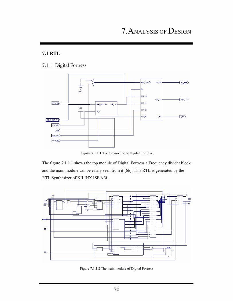
7.ANALYSIS OF DESIGN
7.1 RTL
7.1.1 Digital Fortress
Figure 7.1.1.1 The top module of Digital Fortress
The figure 7.1.1.1 shows the top module of Digital Fortress a Frequency divider block
and the main module can be easily seen from it [66]. This RTL is generated by the
RTL Synthesizer of XILINX ISE 6.3i.
Figure 7.1.1.2 The main module of Digital Fortress
70
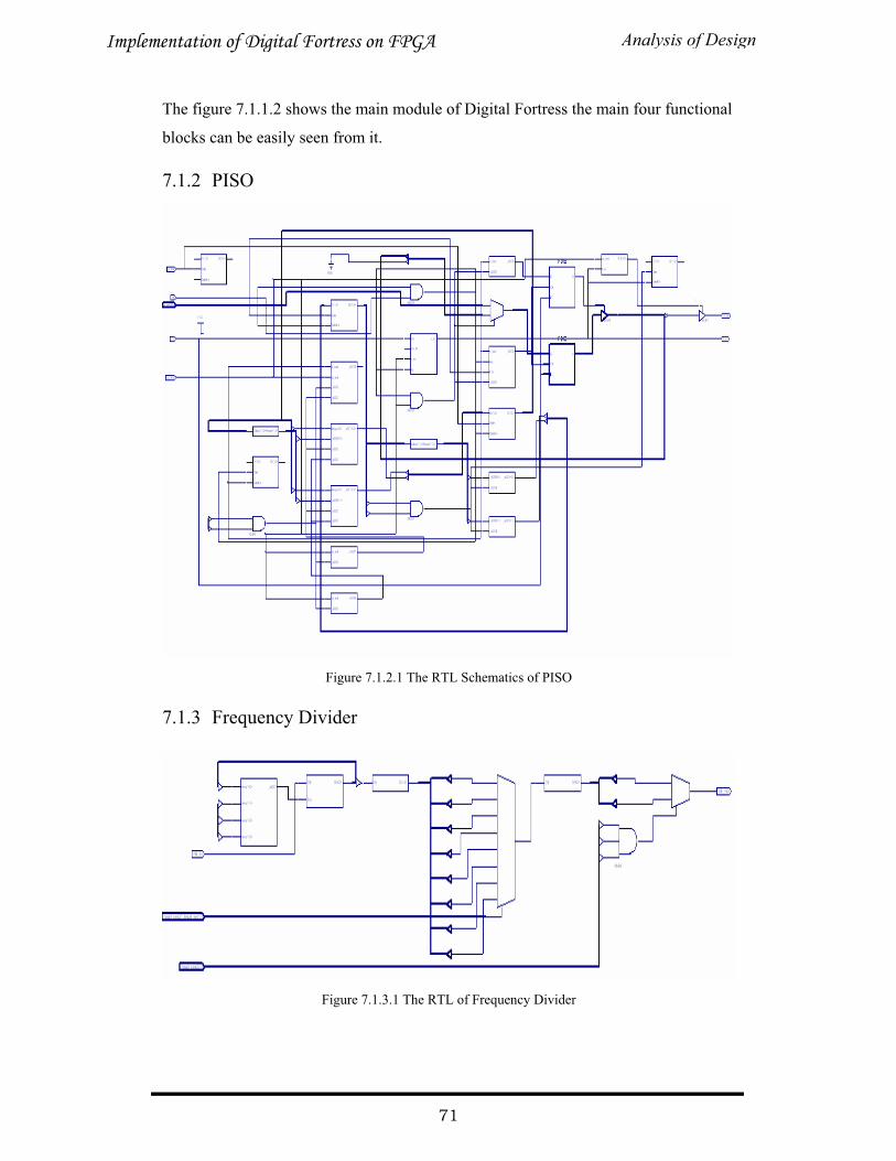
The figure 7.1.1.2 shows the main module of Digital Fortress the main four functional
blocks can be easily seen from it.
7.1.2 PISO
Figure 7.1.2.1 The RTL Schematics of PISO
7.1.3 Frequency Divider
Figure 7.1.3.1 The RTL of Frequency Divider
Analysis of DesignImplementation of Digital Fortress on FPGA
71
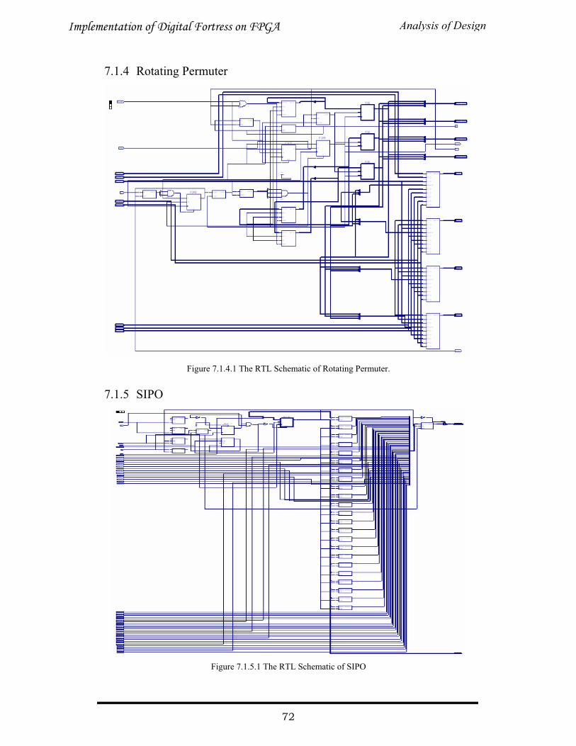
7.1.4 Rotating Permuter
Figure 7.1.4.1 The RTL Schematic of Rotating Permuter.
7.1.5 SIPO
Figure 7.1.5.1 The RTL Schematic of SIPO
Analysis of DesignImplementation of Digital Fortress on FPGA
72
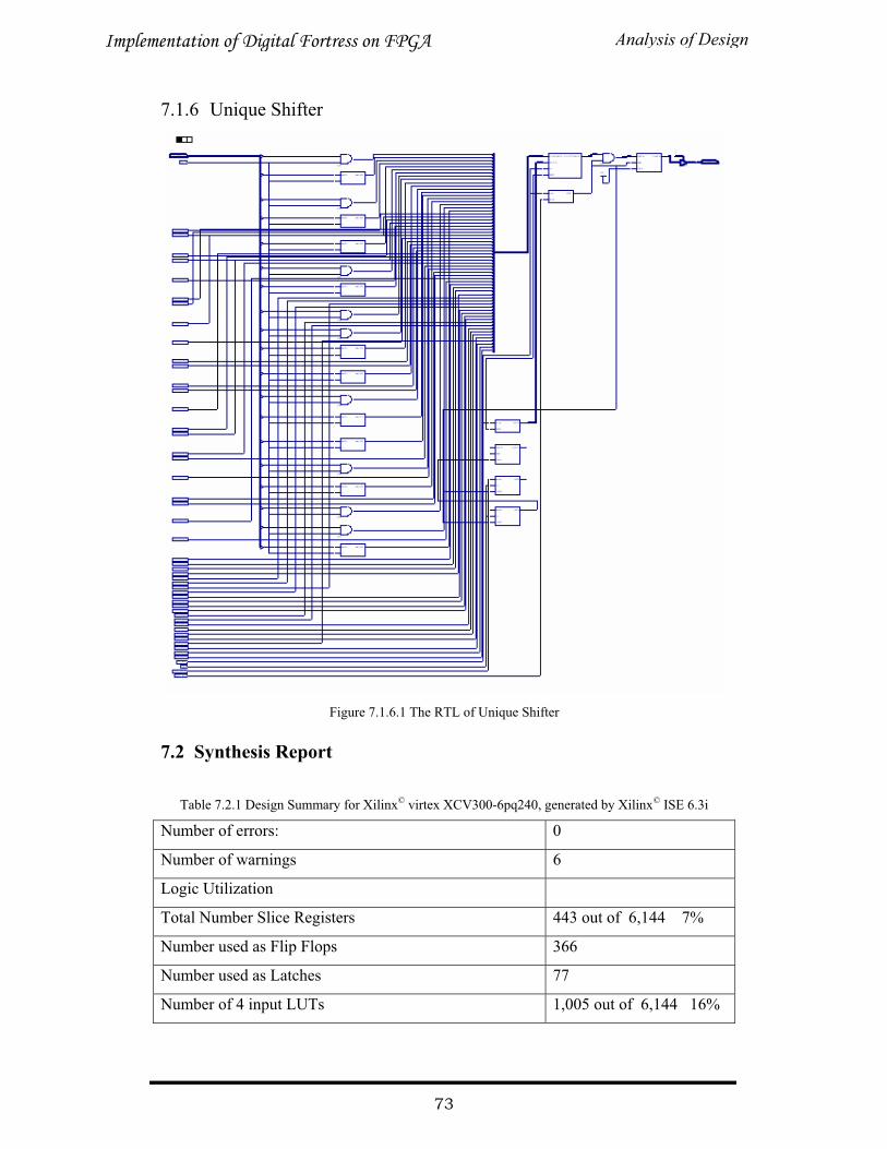
7.1.6 Unique Shifter
Figure 7.1.6.1 The RTL of Unique Shifter
7.2 Synthesis Report
Table 7.2.1 Design Summary for Xilinx© virtex XCV300-6pq240, generated by Xilinx© ISE 6.3i
Number of errors: 0
Number of warnings 6
Logic Utilization
Total Number Slice Registers 443 out of 6,144 7%
Number used as Flip Flops 366
Number used as Latches 77
Number of 4 input LUTs 1,005 out of 6,144 16%
Analysis of DesignImplementation of Digital Fortress on FPGA
73
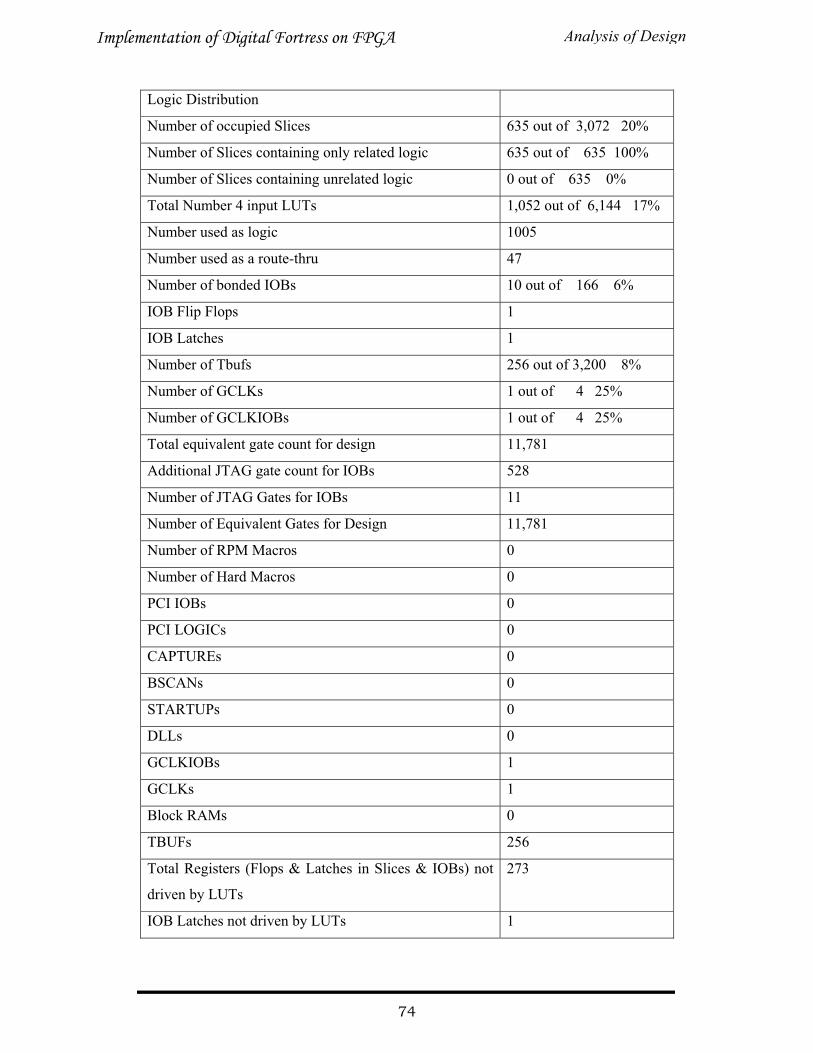
Logic Distribution
Number of occupied Slices 635 out of 3,072 20%
Number of Slices containing only related logic 635 out of 635 100%
Number of Slices containing unrelated logic 0 out of 635 0%
Total Number 4 input LUTs 1,052 out of 6,144 17%
Number used as logic 1005
Number used as a route-thru 47
Number of bonded IOBs 10 out of 166 6%
IOB Flip Flops 1
IOB Latches 1
Number of Tbufs 256 out of 3,200 8%
Number of GCLKs 1 out of 4 25%
Number of GCLKIOBs 1 out of 4 25%
Total equivalent gate count for design 11,781
Additional JTAG gate count for IOBs 528
Number of JTAG Gates for IOBs 11
Number of Equivalent Gates for Design 11,781
Number of RPM Macros 0
Number of Hard Macros 0
PCI IOBs 0
PCI LOGICs 0
CAPTUREs 0
BSCANs 0
STARTUPs 0
DLLs 0
GCLKIOBs 1
GCLKs 1
Block RAMs 0
TBUFs 256
Total Registers (Flops & Latches in Slices & IOBs) not
driven by LUTs
273
IOB Latches not driven by LUTs 1
Analysis of DesignImplementation of Digital Fortress on FPGA
74
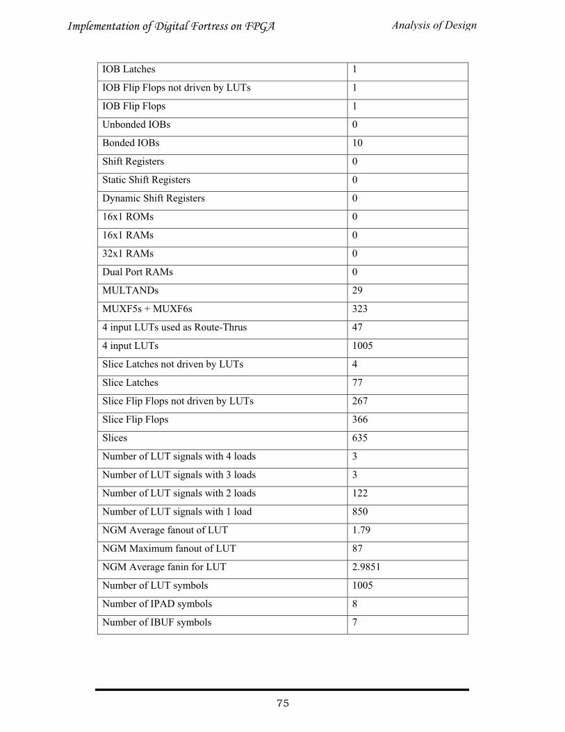
IOB Latches 1
IOB Flip Flops not driven by LUTs 1
IOB Flip Flops 1
Unbonded IOBs 0
Bonded IOBs 10
Shift Registers 0
Static Shift Registers 0
Dynamic Shift Registers 0
16x1 ROMs 0
16x1 RAMs 0
32x1 RAMs 0
Dual Port RAMs 0
MULTANDs 29
MUXF5s + MUXF6s 323
4 input LUTs used as Route-Thrus 47
4 input LUTs 1005
Slice Latches not driven by LUTs 4
Slice Latches 77
Slice Flip Flops not driven by LUTs 267
Slice Flip Flops 366
Slices 635
Number of LUT signals with 4 loads 3
Number of LUT signals with 3 loads 3
Number of LUT signals with 2 loads 122
Number of LUT signals with 1 load 850
NGM Average fanout of LUT 1.79
NGM Maximum fanout of LUT 87
NGM Average fanin for LUT 2.9851
Number of LUT symbols 1005
Number of IPAD symbols 8
Number of IBUF symbols 7
Analysis of DesignImplementation of Digital Fortress on FPGA
75
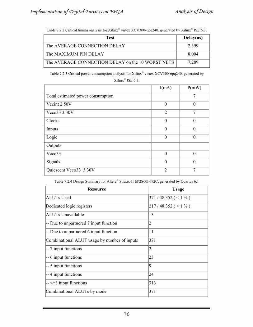
Table 7.2.2.Critical timing analysis for Xilinx© virtex XCV300-6pq240, generated by Xilinx© ISE 6.3i
Test Delay(ns)
The AVERAGE CONNECTION DELAY 2.399
The MAXIMUM PIN DELAY 8.004
The AVERAGE CONNECTION DELAY on the 10 WORST NETS 7.289
Table 7.2.3 Critical power consumption analysis for Xilinx© virtex XCV300-6pq240, generated by
Xilinx© ISE 6.3i
I(mA) P(mW)
Total estimated power consumption 7
Vccint 2.50V 0 0
Vcco33 3.30V 2 7
Clocks 0 0
Inputs 0 0
Logic 0 0
Outputs
Vcco33 0 0
Signals 0 0
Quiescent Vcco33 3.30V 2 7
Table 7.2.4 Design Summary for Altera© Stratix-II EP2S60F672C, generated by Quartus 6.1
Resource Usage
ALUTs Used 371 / 48,352 ( < 1 % )
Dedicated logic registers 217 / 48,352 ( < 1 % )
ALUTs Unavailable 13
-- Due to unpartnered 7 input function 2
-- Due to unpartnered 6 input function 11
Combinational ALUT usage by number of inputs 371
-- 7 input functions 2
-- 6 input functions 23
-- 5 input functions 9
-- 4 input functions 24
-- <=3 input functions 313
Combinational ALUTs by mode 371
Analysis of DesignImplementation of Digital Fortress on FPGA
76

normal mode 313
extended LUT mode 2
arithmetic mode 56
shared arithmetic mode 0
Logic utilization 384 / 48,352 ( < 1 % )
ALUT/register pairs used 371
Combinational with no register 154
register only 0
Combinational with a register 217
ALUT/register pairs unavailable 13
Total registers* 217 / 51,182 ( < 1 % )
Dedicated logic registers 217 / 48,352 ( < 1 % )
I/O registers 0 / 2,830 ( 0 % )
ALMs: partially or completely used 226 / 24,176 ( < 1 % )
Total LABs: partially or completely used 33 / 3,022 ( 1 % )
User inserted logic elements 0
Virtual pins 0
I/O pins 75 / 493 ( 15 % )
Clock pins 7 / 16 ( 44 % )
Global signals 10
M512s 0 / 329 ( 0 % )
M4Ks 0 / 255 ( 0 % )
M-RAMs 0 / 2 ( 0 % )
Total block memory bits 0 / 2,544,192 ( 0 % )
Total block memory implementation bits 0 / 2,544,192 ( 0 % )
DSP block 9-bit elements 3 / 288 ( 1 % )
PLLs 0 / 6 ( 0 % )
Global clocks 10 / 16 ( 63 % )
Regional clocks 0 / 32 ( 0 % )
SERDES transmitters 0 / 84 ( 0 % )
SERDES receivers 0 / 84 ( 0 % )
Analysis of DesignImplementation of Digital Fortress on FPGA
77

Average interconnect usage 0%
Peak interconnect usage 1%
Total fan-out 1898
Average fan-out 2.8
Table 7.2.5 Critical power consumption analysis according to Altera© Stratix-II EP2S60F672C
generated by Quartus 6.1
Device Stratix-II EP2S60F672C
Power Models Final
Total power dissipation 644.71mW
Core Dynamic Thermal Dissipation 0.00mW
Core Static Thermal Dissipation 617.03mW
I/O Thermal Dissipation 27.68mW
7.3 Test bench
7.3.1 Fixed Frequency mode
Figure7.3.1 Fixed frequency mode operation test bench results
Figure 7.3.1 shows the testbench results for normal operation the sequence in which
the signals will execute are as follows.
The system works on active low reset so logic high is provided to the sys_rst pin, now
we will check the default settings of the system so we assign logic high to the sys_tst
pin so that the user should not have to worry about the key and the data to be
provided. Now to enable the operation of the system logic high is given to the sys_en
Analysis of DesignImplementation of Digital Fortress on FPGA
78
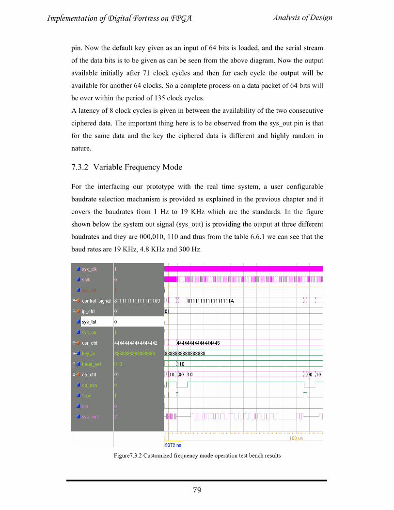
pin. Now the default key given as an input of 64 bits is loaded, and the serial stream
of the data bits is to be given as can be seen from the above diagram. Now the output
available initially after 71 clock cycles and then for each cycle the output will be
available for another 64 clocks. So a complete process on a data packet of 64 bits will
be over within the period of 135 clock cycles.
A latency of 8 clock cycles is given in between the availability of the two consecutive
ciphered data. The important thing here is to be observed from the sys_out pin is that
for the same data and the key the ciphered data is different and highly random in
nature.
7.3.2 Variable Frequency Mode
For the interfacing our prototype with the real time system, a user configurable
baudrate selection mechanism is provided as explained in the previous chapter and it
covers the baudrates from 1 Hz to 19 KHz which are the standards. In the figure
shown below the system out signal (sys_out) is providing the output at three different
baudrates and they are 000,010, 110 and thus from the table 6.6.1 we can see that the
baud rates are 19 KHz, 4.8 KHz and 300 Hz.
Figure7.3.2 Customized frequency mode operation test bench results
Analysis of DesignImplementation of Digital Fortress on FPGA
79
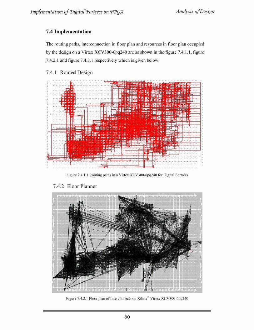
7.4 Implementation
The routing paths, interconnection in floor plan and resources in floor plan occupied
by the design on a Virtex XCV300-6pq240 are as shown in the figure 7.4.1.1, figure
7.4.2.1 and figure 7.4.3.1 respectively which is given below.
7.4.1 Routed Design
Figure 7.4.1.1 Routing paths in a Virtex XCV300-6pq240 for Digital Fortress
7.4.2 Floor Planner
Figure 7.4.2.1 Floor plan of Interconnects on Xilinx© Virtex XCV300-6pq240
Analysis of DesignImplementation of Digital Fortress on FPGA
80
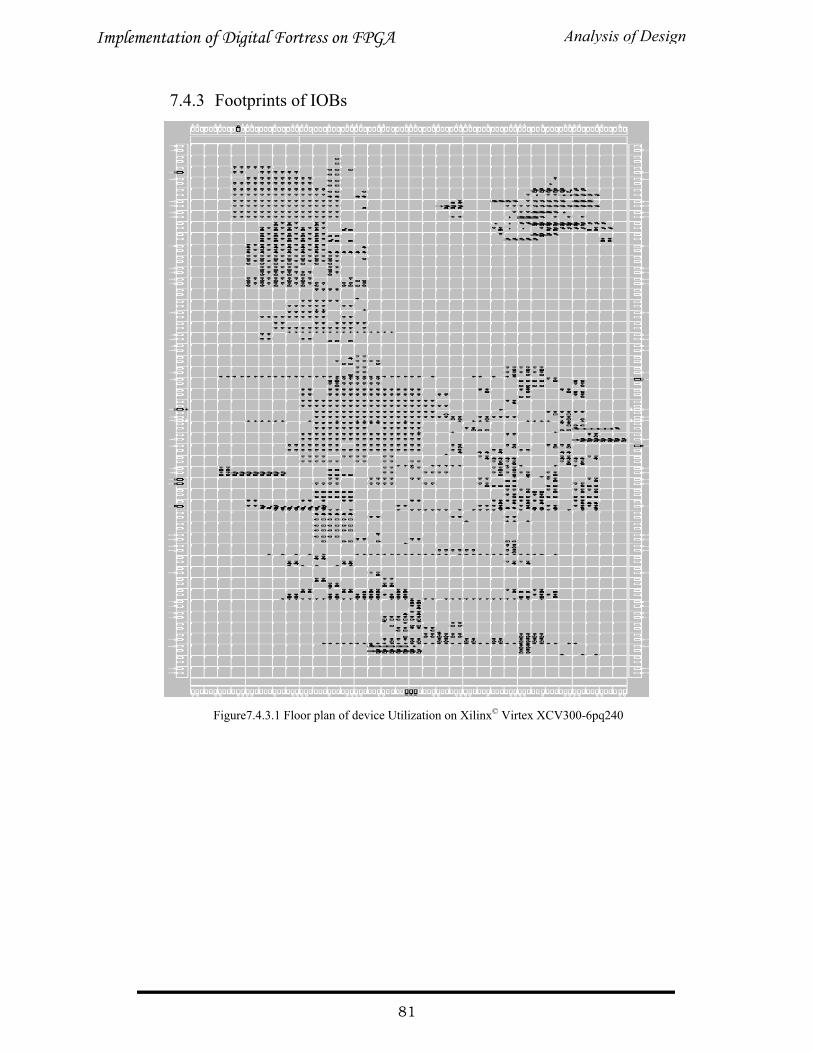
7.4.3 Footprints of IOBs
Figure7.4.3.1 Floor plan of device Utilization on Xilinx© Virtex XCV300-6pq240
Analysis of DesignImplementation of Digital Fortress on FPGA
81
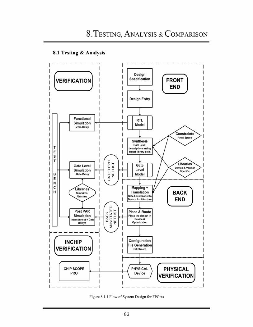
8.TESTING, ANALYSIS & COMPARISON
8.1 Testing & Analysis
Figure 8.1.1 Flow of System Design for FPGAs
82
The figure 8.1.1 shows the generalized flow diagram of the System Design for
FPGAs, the flow includes the designing parts includes front end and back end. The
first task is to describe the design specifications and then the coding in VHDL to
create the RTL model of the design. A synthesis is done based upon the gate level
models available in the libraries. Mapping and translation is performed to make the
design device specific and a place and route for the real time interfacing, the
constraints to be considered here are speed and area. Then a bit stream file is
generated and it is downloaded into the physical device. It’s called the physical
verification. For in chip verification another emulator called Chipscope pro is used.
The major element for the verification is to make the testbench for the design and
provide all the possible test vectors and verify the outputs. While using testbench we
can verify our design in three different simulations….
Functional Simulation
It’s a test for the required function of a unit. Functional tests are independent of
the implementation of the unit under test. Functional tests do not require
implementation knowledge, but test for design errors/correctness. As such,
functional tests do not check for physical hardware faults in the manufactured
system. For instance the functional test of a multiplier unit could be 4 * 7 = 28.
Such tests check that the unit would perform multiplication and handle corner
conditions such as four quadrant signage
Behavioral Simulation
A behavioral simulation uses the VHDL code written in order to model the
behavior of the module under test. Neither gate delays nor interconnect delays are
modeled. Furthermore, functionality of the behavioral model may not match that
of the synthesized logic. Behavioral simulation gives the least accurate prediction
of how the final hardware implementation will perform; it is the most useful form
of simulation during the initial debugging of a design. There is little point in
running more realistic simulations until the behavioral model works correctly.
Testing, Analysis & ComparisonImplementation of Digital Fortress on FPGA
83
NON Behavioral Simulation
� Post-Translation Simulation
A post-translation simulation uses the synthesized gate-level netlist to model
the module under test. The functionality of the gates is modeled using a
generic Xilinx library, but propagation delay is not modeled. The simulation
should match the behavior of the actual hardware, but will assume the
hardware is infinitely fast. In a post-mapping simulation, the gates have been
mapped to a library specific to the FPGA device being targeted. This library
includes accurate gate delay information. However, interconnect delay is not
modeled, because the design at this stage has not yet been placed and routed.
� Post-Place-and-Route Simulation
A post-place-and-route simulation models interconnect delay, as well as gate
delay. This type of simulation will most accurately match the behavior of the
actual hardware. However, for large designs, it can take a significant amount
of time to extract the interconnect delay values from the place-and-route
information, and a significant amount of time to run the actual simulation. It
really only makes sense to perform post-place-and-route simulations at the
top level of a design. If one performs a post-place-and-route simulation on a
sub module, the place-and-route process is rerun, using the sub module as the
top-level of the design. The interconnect delays for the sub module
simulation will therefore not match the interconnect delays for that sub
module when it is laid out as part of the complete project.
8.2 Comparison
8.2.1 Digital Fortress V/S Rest of Crypto World
The table 8.2.1 shows the comparison of the proposed algorithm Digital Fortress with
the existing algorithms which are standardized for encryption process or strong
contenders for the standardization. The data is mainly taken from the companies or
research group websites, involved in developing different encryption algorithms and
analyzing their hardware performances. The performance parameters are divided into
four major categories Size/Area, Speed (MHz) and the Throughput (Mbps). Though
Testing, Analysis & ComparisonImplementation of Digital Fortress on FPGA
84
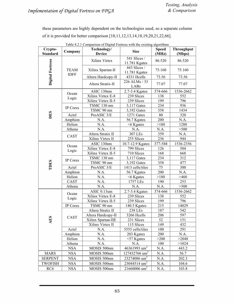
these parameters are highly dependent on the technologies used, so a separate column
of it is provided for better comparison [10,11,12,13,14,18,19,20,21,22,66].
Table 8.2.1 Comparison of Digital Fortress with the existing algorithms Crypto-
Standard Company Technology/ Device Size Speed
(MHz) Throughput
(Mbps)
Xilinx Virtex 541 Slices / 11.781 Kgates 86.520 86.520
Xilinx Spartan-II 443 Slices / 11.781 Kgates 75.160 75.160
Altera Hardcopy-II 4331 Hcells 73.56 73.56
Dig
ital F
ortr
ess
TEAMIDFF
Altera Stratix-II 226 ALMs / 33 LABs 77.07 77.07
ASIC 130nm 2.7-3.4 Kgates 374-666 1536-2662 Xilinx Virtex E-8 239 Slices 138 552Ocean
LogicXilinx Virtex II-5 239 Slices 199 796
TSMC 130 nm 3,117 Gates 234 936IP Cores TSMC 90 nm 3,192 Gates 358 1434Actel ProASIC 3/E 1271 Gates 80 320
Amphion N.A. 56.7 Kgates 200 N.A.Helion N.A. <6 Kgates >180 1280Athena N.A. N.A. N.A. >500
Altera Stratix II 307 LEs 359 N.A.
DE
S
CAST Xilinx Virtex II 255 Slices 236 944ASIC 130nm 10.7-12.9 Kgates 377-588 1536-2356
Xilinx Virtex E-8 799 Slices 126 504OceanLogic
Xilinx Virtex II-5 710 Slices 168 668TSMC 130 nm 3,117 Gates 234 312IP Cores TSMC 90 nm 3,192 Gates 358 477
Actel ProASIC 3/E 1413 cells/tiles 75 300Amphion N.A. 56.7 Kgates 200 N.A.
Helion N.A. <6 Kgates >180 >460CAST N.A. 1757 LEs 190 253
TD
ES
Athena N.A. N.A. N.A. >500ASIC 0.13um 2.7-3.4 Kgates 374-666 1536-2662
Xilinx Virtex E-8 239 Slices 138 552OceanLogic
Xilinx Virtex II-5 239 Slices 199 796IP Cores TSMC 90 nm 140.5 Kgates 215 14029
Altera Stratix II 238 LEs 187 542Altera Hardcopy-II 3266 Hcells 206 597Xilinx Spartan-IIE 231 Slices 52 151CAST
Xilinx Virtex II 115 Slices 149 432Actel N.A. 5555 cells/tiles 100 291
Amphion N.A. 203 Kgates 200 N.A.Helion N.A. <57 Kgates >200 >2048Athena N.A. N.A. 100 >1024
AE
S
NSA MOSIS 500nm 46361993 um2 N.A. 443.2 MARS NSA MOSIS 500nm 127432766 um2 N.A. 56.7
SERPENT NSA MOSIS 500nm 23274086 um2 N.A. 202.3 TWOFISH NSA MOSIS 500nm 23044514 um2 N.A. 104.6
RC6 NSA MOSIS 500nm 21660006 um2 N.A. 103.8
Testing, Analysis & ComparisonImplementation of Digital Fortress on FPGA
85

8.3 Problems & Solutions
8.3.1 Strengths
� We have the well defined path to follow.
� The algorithm is well defined and easily understood.
� We have scheduled each and every task to be performed.
� The simulations were verified with the desired outputs.
8.3.2 Difficulties Faced
� Synchronization between the functionalities of SIPO-serial in parallel out and
PISO-parallel in serial out.
� In the designing of rotator block we wanted to shift all the 64 bits to be shifted on
a single clock pulse for the faster computations in the range of 0 to 63 bits.
� Arithmetic operations like mod we have to find a similar in functionality but
different in implementation as mod can be operated only on the operands with
power of 2.
8.3.3 Proposed Solutions
� The whole system is designed using acknowledgement mechanism. And a control
register and status register are implemented for better synchronization [66].
� A rotator block a barrel shifter concept is designed to shift the 64 bits on a single
clock pulse to achieve the maximum through put for the system [66].
� For the “mod” operator we defined a new logic on the basis of divide and
conquer approach with help of XORed logic[66].
The proof of divide & conquer approach:
Suppose x, y, z, d, e, f, g, h, p, q, r, s and n are variables and c is a constant.
Assume that x y z nc d � 8.3.3.1
And,
Testing, Analysis & ComparisonImplementation of Digital Fortress on FPGA
86
x pc e� 8.3.3.2
y qc f� 8.3.3.3
z rc g� 8.3.3.4
e f g sc h � 8.3.3.5
Putting 8.3.3.2, 8.3.3.3 and 8.3.3.4 into 8.3.3.1 we get,
( )p q r c e f g nc d � 8.3.3.6
Putting 8.3.3.5 into 8.3.3.6 we get,
( )p q r c sc h nc d � 8.3.3.7
( )p q r s c h nc d � 8.3.3.8
Comparing both the sides of 8.3.3.8
( )n p q r s�
And d h�
So the out come of the above logic concludes that a very large number can be factored
and used for further process without any kind of alteration in the final results [65]. In
a nut shell this proof states that,
( ) m o d 2 ( m o d 2 m o d 2 m o d 2 ) m o d 2a b c a b c �
Testing, Analysis & ComparisonImplementation of Digital Fortress on FPGA
87
9.CONCLUSION & FUTURE SCOPE
Digital Fortress is a proposed crypto algorithm which is enhanced and modified
version of Vernam’s OTP to attain a state of Perfect Secrecy which lead algorithm to
the pinnacle of secrecy so all the attack fails against it. By this algorithm Perfect
Secrecy is achieved by randomizing finite small Key by Rotating Key Function to
support Permuted XORing which utilizes the Rotating Permutation, Modified
XORing and Rotating Odd Shifter. This algorithm performs all the basic function in
its primitive form so computing power requirement is very low. Proposed algorithm is
immune towards all kind of existing attack which is shown in simulation result and
proven by mathematical formulas given by Perfect Secrecy Theory. The added
advantage of this algorithm is that each and every block of it is completely reversible
and thus no separate algorithm of any hardware is required. Proposed algorithm is in
its basic form and many other enhancements can be included.
As a part of this project work the algorithm is implemented on VHDL. The initial
prototype of it just operates in serial mode only as a RS232 connector is readily
available on the Xilinx Virtex XCV300 board. So the prototype can be extended to
perform on the parallel data packets also. The initial design consumes nearly
12Kgates and it has considerable power consumption which can be reduced by its
ASIC realization. It can perform extremely well when used as a co-processor in any
system.
The added advantage of this algorithm is that it is completely invertible in nature,
hence no need of a separate decryption algorithm or other hardware.
Moreover, this algorithm is answer to the requirement of modern communication
system like low computation power, lower time for execution and immune to attack.
In future an indigenous hardware prototype can be modeled for the same algorithm
and an interfacing of it with real-time systems can be done. As theory point of view a
detailed mathematical analysis of the Digital Fortress algorithm can be done and its
immunity on different kind of attacks can be verified to check its reliability.
88
10. REFERENCES
10.1 Internet Resources
1. http://en.wikipedia.org/wiki/Cryptography 4/18/2007
2. Tom Dunigan’s Security Page-
http://www.csm.ornl.gov/~dunigan/security.html
3. The Cryptography FAQ-
http://www.faqs.org/faqs/cryptography-faq/
4. http://world.std.com/~franl/crypto.html
5. Computer Security Resource Center- http://csrc.nist.gov/
6. American Cryptogram Association-
http://www.cryptogram.org/cipher_types.html
7. AES Home Page; The Rijandel Page-
http://www.iaik.tugraz.at/research/krypto/AES/old/~rijmen/rijndael/
8. Block Cipher Lounge-
http://www2.mat.dtu.dk/people/Lars.R.Knudsen/aes.html
9. NIST Random Number Generation Technical Working Group-
http://csrc.nist.gov/rng/rng3.html
10. http://www.xilinx.com/
11. https://www.altera.com/support/software/download/
12. http://www.opencores.org/browse.cgi/by_category
13. http://www.ocean-logic.com/des.htm
14. http://www.nsa.gov/research/resea00003.cfm
15. http://www.deviceforge.com/articles/AT4234154468.html
16. http://csrc.nist.gov/CryptoToolkit/
17. http://www.cryptool.com/
18. http://www.ipcores.com/DES1core.htm
19. http://www.actel.com/techdocs/ds/ip.aspx
20. http://www.conexant.com/products/entry.jsp?id=181
21. http://www.heliontech.com/enc.htm
22. http://www.athena-group.com/encryption.htm
89
10.2 Books, Journals, Articles
� Books
23. D. Welsh; Codes & Cryptography; Oxford Science Publication, London,
1988.
24. J. A. Buchmann; Introduction to Cryptography; Springer-Verlag, New York,
2001 (second edition).
25. Stinson; Cryptography, Theory & Practice; CRC Press, Florida, 2002 (second
edition).
26. J. Menezes, S. A. Vanstone, and D. C. V. Oorschot; Hand-book of Applied
Cryptography; CRC Press, Florida, 1996.
27. M. Rozenblit; Security for Telecommunications Network Management; IEEE
Press Series on Network Management, Wiley-IEEE Press, 1999.
28. V. LeVeque; Information Security: A Strategic Approach; Wiley-IEEE
Computer Society Press, 2006.
� Journals
29. G. Vernam; “Vernam's cipher”; Bell System Technology Journal, 1918.
30. C. E. Shannon; “Communication Theory of Secrecy Systems”; Bell System
Technology Journal, 1949.
� Standards
31. “Data Encryption Standard”; FIPS (Federal Information Processing Standard)
Publication 46-3; U. S. Department of Commerce / National Institute of
Standards & Technology, USA, 1999.
32. “Security Requirements for cryptographic modules”; FIPS (Federal
Information Processing Standard) Publication 140-1; U. S. Department of
Commerce / National Institute of Standards & Technology, USA, 1994.
33. “Glossary for Computer System Security”; FIPS (Federal Information
Processing Standard) Publication 39; U. S. Department of Commerce /
National Institute of Standards & Technology, USA, 2001.
ReferencesImplementation of Digital Fortress on FPGA
90

34. “Advanced Encryption Standard”; FIPS (Federal Information Processing
Standard) Publication 197; U. S. Department of Commerce / National Institute
of Standards & Technology, USA, 2001.
� Report
35. B. Weeks, M. Bean, T. Rozylowicz and C. Ficke ; “Hardware Performance
Simulations of Round 2 Advanced Encryption Standard Algorithms”; National
Security Agency,USA,1999.
36. J. Daemen and V. Rijmen ; “AES Proposal: Rijndael” ; Document version 2,
Date: 03/09/99.
� Articles
37. W. Burr, National Institute of Standards & Technology, USA; “Selecting the
Advanced Encryption Standard”; IEEE Security & Privacy Magazine ,The
IEEE Computer Society , March/April 2003.
38. K. G. Paterson and A. K. L. Yau, Royal Hallway, University of London ;
“Lost in Translation: Theory and Practice in Cryptography”; IEEE Security
& Privacy Magazine ,The IEEE Computer Society , May/June 2006.
39. R. Gennarao, IBM T. J., Watson Research Center; “Randomness in
Cryptography”; IEEE Security & Privacy Magazine ,The IEEE Computer
Society , March/April 2006.
40. J. Coron, University of Luxembourg; “What Is Cryptography?”; IEEE
Security & Privacy Magazine ,The IEEE Computer Society , January/
February 2006.
10.3 Research Papers
41. K. Jarvinen, M. Tommiska and J. Skytta; “Comparative survey of high-
performance cryptographic algorithm implementations on FPGAs”; IEE
Proceedings online no. 20055004.
42. M. Feldhofer, J. Wolkerstorfer and V. Rijmen; “AES implementation on a
grain of sand”; IEE Proceedings online no. 20055006
43. S. F. Hsiao, M. C. Chen, M. Y. Tsai and C. C. Lin; “System-on-chip
implementation of the whole advanced encryption standard processor using
ReferencesImplementation of Digital Fortress on FPGA
91
reduced XOR-based sum-of-product operations”; IEE Proceedings online no.
20055005.
44. T. Kerins, W.P. Marnane, E.M. Popovici and P.S.L.M. Barreto; “Hardware
accelerators for pairing based Cryptosystems”; IEE Proceedings online no.
20055009.
45. S. R. Blackburn, C. F. A. Cid and S. D. Galbraith; “Cryptanalysis of a
cryptosystem based on Drinfeld Modules”; IEE Proceedings online no.
20055035.
46. Z. A. Kissel; “Obfuscation of The Standard XOR Encryption Algorithm”;
Crossroads, The ACM Student Magazine, 2004.
47. E. R. Henriquez, N. A. Saqib and A. D. Pkrez, “4.2 Gbit/s single-chip FPGA
implementation of AES algorithm”; Electronics letters, Vol 39, No 15, July
2003.
48. M. McLoone and J. V. McCanny “High-performance FPGA implementation
of DES using a novel method for implementing the key schedule”, IEE Proc.-
Circuits Devices Syst., Vol. 150, No. 5, October 2003
49. A. Hodjat and I. Verbauwhede; “A 21.54 Gbits/s Fully Pipelined AES
Processor on FPGA”; Proceedings of the 12th Annual IEEE Symposium on
Field-Programmable Custom Computing Machines, 2004.
50. S. F. Hsiao, M. C. Chen, M. Y. Tsai and C. C. Lin; “System-on-chip
implementation of the whole advanced encryption standard processor using
reduced XOR-based sum-of-product operations”; IEE Proceedings
Information Security, 2005.
51. C. J. McIvor, M. McLoone and J. V. McCanny ; “Hardware Elliptic Curve
Cryptographic Processor Over GF(p)”; IEEE Transaction on Circuits and
Systems, Vol. 53, No. 9, September 2006
52. M. McLoone and J. V. McCanny ; “High-performance FPGA implementation
of DES using a novel method for implementing the key schedule”; IEE
Proceeding Circuits Devices Syst., Vol. 150, No. 5, October 2003
53. R. Sever, A. N. Ismailoglu, Y. C. Tekmen, M. Askar , B. Okcan ; “A High
Speed Fpga Implementation Of The Rijndael Algorithm”; Proceedings of the
EUROMICRO Systems on Digital System Design,IEEE,2004.
54. G. Rouvroy, F. X. Standaert, J. J. Quisquater and J. D. Legat; “Compact and
Efficient Encryption/Decryption Module for FPGA Implementation of the AES
ReferencesImplementation of Digital Fortress on FPGA
92
Rijndael Very Well Suited for Small Embedded Applications”; Proceedings of
the International Conference on Information Technology: Coding and
Computing, Las Vegas, USA,2004.
55. S J Shepherd; “Public Key Stream Ciphers”; IEE Colloquium on Security &
Cryptography Applications to Radio Systems, London, 1994.
56. J. C. Cooke and R. L. Brewster; “Cryptographic Algorithms and Protocols for
Personal Communication Systems Security”; IEE Colloquium on Security &
Cryptography Applications to Radio Systems, London, 1994.
57. Prof. F. C. Piper; “The Management of Security”; IEE Colloquium on
Security & Cryptography Applications to Radio Systems, London, 1994.
58. Prof. F. C. Piper; “Basic Principles of Cryptography”; IEE Colloquium on
Public Uses of Cryptography, London, 1996.
59. M. J. Stirland; “Cryptography in Payments Systems”; IEE Colloquium on
Public Uses of Cryptography, London, 1996.
60. A. Aziz and N. Ikram; “An Efficient FPGA Based Sequential Implementation
Of Advanced Encryption Standard”. 3rd International Conference on
Information and Communication Technology, Egypt, 2005
61. I. Kim, C. S. Steele, J. G. Koller; “A Fully Pipelined, 700MBytes/s DES
Encryption Core”;9th Great Lakes Symposium on VLSI, Michigan, USA,1999
62. K. Wong, M. Wark and E. Dawson ; “A Single-Chip FPGA Implementation
Of The Data Encryption Standard (DES) Algorithm”; Global
Telecommunications Conference, Austratilia, 1998
63. T. Arich, E. Mohammadia, I. Sina, A. Rabat; “Hardware implementations of
the Data Encryption Standard”.; 14th International conference on
Microelectronics, Lebanon, 2002
10.4 Publications
64. “Digital Fortress [New Standard for Encryption]”; Defense & Security
Symposium 07, SPIE; Orlando, Florida, U.S.A., April- 2007
65. “Digital Fortress-An extended version”; Crypto 07, International Association
for Cryptologic Research; Santa Barbara, California, U.S.A., August-2007
ReferencesImplementation of Digital Fortress on FPGA
93
66. “Design, Simulation and Implementation of Digital Fortress on FPGA”;
Design Techniques for Modern Electronic Devices, VLSI & Communication
system, VLSI Society of India; NIT, Hamirpur, India, May-2007
67. “Comparison of Digital Fortress with AES”, National Level Symposium on
Security & Soft Computing; SVNIT, Surat, India March-2007
ReferencesImplementation of Digital Fortress on FPGA
94
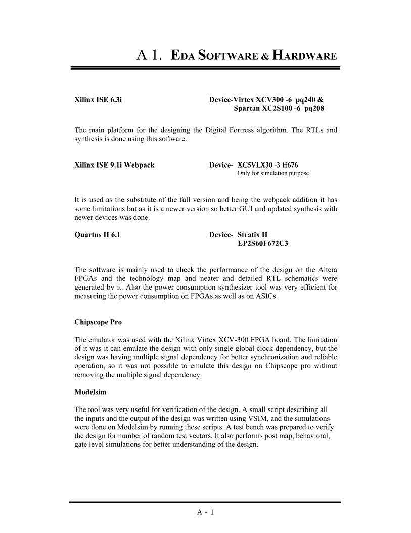
A 1. EDA SOFTWARE & HARDWARE
Xilinx ISE 6.3i Device-Virtex XCV300 -6 pq240 & Spartan XC2S100 -6 pq208
The main platform for the designing the Digital Fortress algorithm. The RTLs and synthesis is done using this software.
Xilinx ISE 9.1i Webpack Device- XC5VLX30 -3 ff676Only for simulation purpose
It is used as the substitute of the full version and being the webpack addition it has some limitations but as it is a newer version so better GUI and updated synthesis with newer devices was done.
Quartus II 6.1 Device- Stratix II EP2S60F672C3
The software is mainly used to check the performance of the design on the Altera FPGAs and the technology map and neater and detailed RTL schematics were generated by it. Also the power consumption synthesizer tool was very efficient for measuring the power consumption on FPGAs as well as on ASICs.
Chipscope Pro
The emulator was used with the Xilinx Virtex XCV-300 FPGA board. The limitation of it was it can emulate the design with only single global clock dependency, but the design was having multiple signal dependency for better synchronization and reliable operation, so it was not possible to emulate this design on Chipscope pro without removing the multiple signal dependency.
Modelsim
The tool was very useful for verification of the design. A small script describing all the inputs and the output of the design was written using VSIM, and the simulations were done on Modelsim by running these scripts. A test bench was prepared to verify the design for number of random test vectors. It also performs post map, behavioral, gate level simulations for better understanding of the design.
A - 1
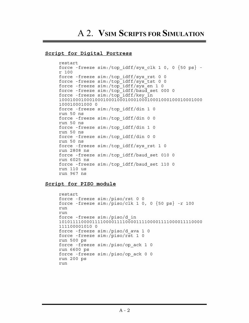
A 2. VSIM SCRIPTS FOR SIMULATION
Script for Digital Fortress
restart force -freeze sim:/top_idff/sys_clk 1 0, 0 {50 ps} -r 100 force -freeze sim:/top_idff/sys_rst 0 0 force -freeze sim:/top_idff/sys_tst 0 0 force -freeze sim:/top_idff/sys_en 1 0 force -freeze sim:/top_idff/baud_set 000 0 force -freeze sim:/top_idff/key_in 1000100010001000100010001000100010001000100010001000100010001000 0 force -freeze sim:/top_idff/din 1 0 run 50 ns force -freeze sim:/top_idff/din 0 0 run 50 ns force -freeze sim:/top_idff/din 1 0 run 50 ns force -freeze sim:/top_idff/din 0 0 run 50 ns force -freeze sim:/top_idff/sys_rst 1 0 run 2808 ns force -freeze sim:/top_idff/baud_set 010 0 run 6025 ns force -freeze sim:/top_idff/baud_set 110 0 run 110 us run 967 ns
Script for PISO module
restart force -freeze sim:/piso/rst 0 0 force -freeze sim:/piso/clk 1 0, 0 {50 ps} -r 100 run run force -freeze sim:/piso/d_in 1010111100001111000011110000111100001111000011110000111100001010 0 force -freeze sim:/piso/d_ava 1 0 force -freeze sim:/piso/rst 1 0 run 500 ps force -freeze sim:/piso/op_ack 1 0 run 6600 ps force -freeze sim:/piso/op_ack 0 0 run 200 ps run
A - 2
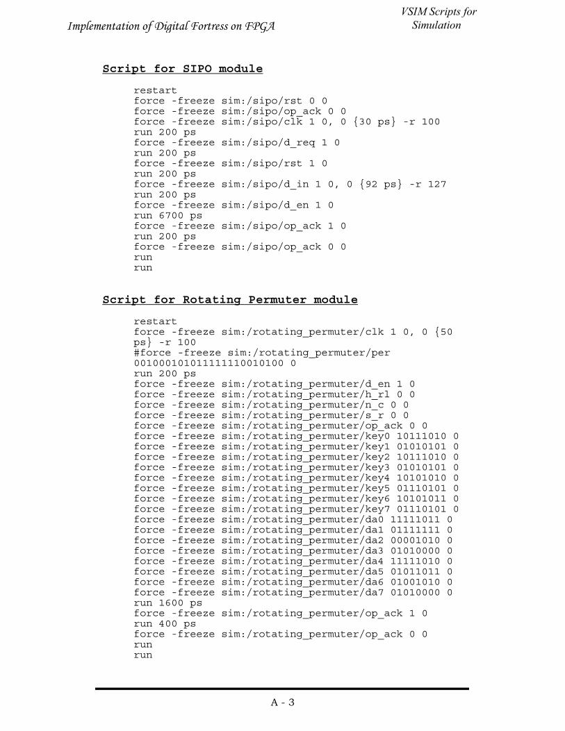
Script for SIPO module
restart force -freeze sim:/sipo/rst 0 0 force -freeze sim:/sipo/op_ack 0 0 force -freeze sim:/sipo/clk 1 0, 0 {30 ps} -r 100 run 200 ps force -freeze sim:/sipo/d_req 1 0 run 200 ps force -freeze sim:/sipo/rst 1 0 run 200 ps force -freeze sim:/sipo/d_in 1 0, 0 {92 ps} -r 127 run 200 ps force -freeze sim:/sipo/d_en 1 0 run 6700 ps force -freeze sim:/sipo/op_ack 1 0 run 200 ps force -freeze sim:/sipo/op_ack 0 0 run run
Script for Rotating Permuter module
restart force -freeze sim:/rotating_permuter/clk 1 0, 0 {50 ps} -r 100 #force -freeze sim:/rotating_permuter/per 001000101011111110010100 0 run 200 ps force -freeze sim:/rotating_permuter/d_en 1 0 force -freeze sim:/rotating_permuter/h_rl 0 0 force -freeze sim:/rotating_permuter/n_c 0 0 force -freeze sim:/rotating_permuter/s_r 0 0 force -freeze sim:/rotating_permuter/op_ack 0 0 force -freeze sim:/rotating_permuter/key0 10111010 0 force -freeze sim:/rotating_permuter/key1 01010101 0 force -freeze sim:/rotating_permuter/key2 10111010 0 force -freeze sim:/rotating_permuter/key3 01010101 0 force -freeze sim:/rotating_permuter/key4 10101010 0 force -freeze sim:/rotating_permuter/key5 01110101 0 force -freeze sim:/rotating_permuter/key6 10101011 0 force -freeze sim:/rotating_permuter/key7 01110101 0 force -freeze sim:/rotating_permuter/da0 11111011 0 force -freeze sim:/rotating_permuter/da1 01111111 0 force -freeze sim:/rotating_permuter/da2 00001010 0 force -freeze sim:/rotating_permuter/da3 01010000 0 force -freeze sim:/rotating_permuter/da4 11111010 0 force -freeze sim:/rotating_permuter/da5 01011011 0 force -freeze sim:/rotating_permuter/da6 01001010 0 force -freeze sim:/rotating_permuter/da7 01010000 0 run 1600 ps force -freeze sim:/rotating_permuter/op_ack 1 0 run 400 ps force -freeze sim:/rotating_permuter/op_ack 0 0 run run
VSIM Scripts for Simulation
A - 3
Implementation of Digital Fortress on FPGA
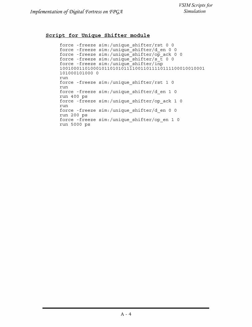
Script for Unique Shifter module
force -freeze sim:/unique_shifter/rst 0 0 force -freeze sim:/unique_shifter/d_en 0 0 force -freeze sim:/unique_shifter/op_ack 0 0 force -freeze sim:/unique_shifter/s_t 0 0 force -freeze sim:/unique_shifter/inp 1001000110100010110101011110011011110111100010010001101000101000 0 run force -freeze sim:/unique_shifter/rst 1 0 run force -freeze sim:/unique_shifter/d_en 1 0 run 400 ps force -freeze sim:/unique_shifter/op_ack 1 0 run force -freeze sim:/unique_shifter/d_en 0 0 run 200 ps force -freeze sim:/unique_shifter/op_en 1 0 run 5000 ps
VSIM Scripts for Simulation
A - 4
Implementation of Digital Fortress on FPGA
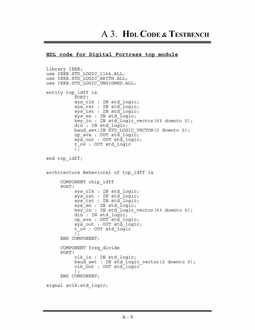
A 3. HDL CODE & TESTBENCH
HDL code for Digital Fortress top module library IEEE; use IEEE.STD_LOGIC_1164.ALL; use IEEE.STD_LOGIC_ARITH.ALL; use IEEE.STD_LOGIC_UNSIGNED.ALL; entity top_idff is PORT( sys_clk : IN std_logic; sys_rst : IN std_logic; sys_tst : IN std_logic; sys_en : IN std_logic; key_in : IN std_logic_vector(63 downto 0); din : IN std_logic; baud_set:IN STD_LOGIC_VECTOR(2 downto 0); op_ava : OUT std_logic; sys_out : OUT std_logic; t_ov : OUT std_logic ); end top_idff; architecture Behavioral of top_idff is COMPONENT chip_idff PORT( sys_clk : IN std_logic; sys_rst : IN std_logic; sys_tst : IN std_logic; sys_en : IN std_logic; key_in : IN std_logic_vector(63 downto 0); din : IN std_logic; op_ava : OUT std_logic; sys_out : OUT std_logic; t_ov : OUT std_logic ); END COMPONENT; COMPONENT freq_divide PORT( clk_in : IN std_logic; baud_set : IN std_logic_vector(2 downto 0); clk_out : OUT std_logic ); END COMPONENT; signal sclk:std_logic;
A - 5
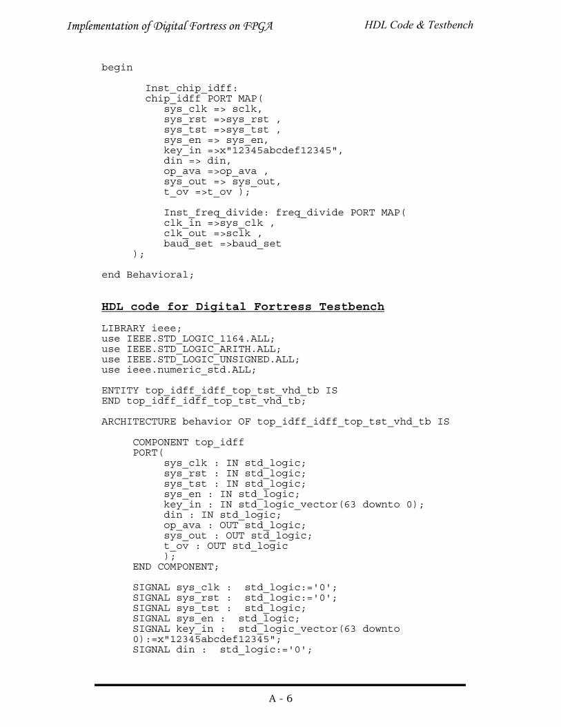
begin Inst_chip_idff: chip_idff PORT MAP( sys_clk => sclk, sys_rst =>sys_rst , sys_tst =>sys_tst , sys_en => sys_en, key_in =>x"12345abcdef12345", din => din, op_ava =>op_ava , sys_out => sys_out, t_ov =>t_ov ); Inst_freq_divide: freq_divide PORT MAP( clk_in =>sys_clk , clk_out =>sclk , baud_set =>baud_set ); end Behavioral; HDL code for Digital Fortress Testbench LIBRARY ieee; use IEEE.STD_LOGIC_1164.ALL; use IEEE.STD_LOGIC_ARITH.ALL; use IEEE.STD_LOGIC_UNSIGNED.ALL; use ieee.numeric_std.ALL; ENTITY top_idff_idff_top_tst_vhd_tb IS END top_idff_idff_top_tst_vhd_tb; ARCHITECTURE behavior OF top_idff_idff_top_tst_vhd_tb IS COMPONENT top_idff PORT( sys_clk : IN std_logic; sys_rst : IN std_logic; sys_tst : IN std_logic; sys_en : IN std_logic; key_in : IN std_logic_vector(63 downto 0); din : IN std_logic; op_ava : OUT std_logic; sys_out : OUT std_logic; t_ov : OUT std_logic ); END COMPONENT; SIGNAL sys_clk : std_logic:='0'; SIGNAL sys_rst : std_logic:='0'; SIGNAL sys_tst : std_logic; SIGNAL sys_en : std_logic; SIGNAL key_in : std_logic_vector(63 downto
0):=x"12345abcdef12345"; SIGNAL din : std_logic:='0';
HDL Code & Testbench
A - 6
Implementation of Digital Fortress on FPGA
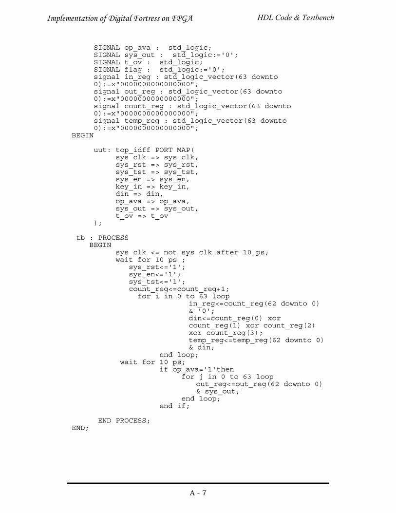
SIGNAL op_ava : std_logic; SIGNAL sys_out : std_logic:='0'; SIGNAL t_ov : std_logic; SIGNAL flag : std_logic:='0'; signal in_reg : std_logic_vector(63 downto
0):=x"0000000000000000"; signal out_reg : std_logic_vector(63 downto
0):=x"0000000000000000"; signal count_reg : std_logic_vector(63 downto
0):=x"0000000000000000"; signal temp_reg : std_logic_vector(63 downto
0):=x"0000000000000000"; BEGIN uut: top_idff PORT MAP( sys_clk => sys_clk, sys_rst => sys_rst, sys_tst => sys_tst, sys_en => sys_en, key_in => key_in, din => din, op_ava => op_ava, sys_out => sys_out, t_ov => t_ov ); tb : PROCESS BEGIN sys_clk <= not sys_clk after 10 ps; wait for 10 ps ; sys_rst<='1'; sys_en<='1'; sys_tst<='1'; count_reg<=count_reg+1; for i in 0 to 63 loop in_reg<=count_reg(62 downto 0)
& '0'; din<=count_reg(0) xor
count_reg(1) xor count_reg(2) xor count_reg(3);
temp_reg<=temp_reg(62 downto 0) & din;
end loop; wait for 10 ps; if op_ava='1'then for j in 0 to 63 loop
out_reg<=out_reg(62 downto 0) & sys_out;
end loop; end if; END PROCESS; END;
HDL Code & Testbench
A - 7
Implementation of Digital Fortress on FPGA