IEEE TRANSACTIONS ON VERY LARGE SCALE...
12
IEEE TRANSACTIONS ON VERY LARGE SCALE INTEGRATION (VLSI) SYSTEMS, VOL. 22, NO. 4, APRIL 2014 759 32 Bit×32 Bit Multiprecision Razor-Based Dynamic Voltage Scaling Multiplier With Operands Scheduler Xiaoxiao Zhang, Student Member, IEEE, Farid Boussaid, Senior Member, IEEE, and Amine Bermak, Fellow, IEEE Abstract—In this paper, we present a multiprecision (MP) reconfigurable multiplier that incorporates variable precision, parallel processing (PP), razor-based dynamic voltage scaling (DVS), and dedicated MP operands scheduling to provide opti- mum performance for a variety of operating conditions. All of the building blocks of the proposed reconfigurable multiplier can either work as independent smaller-precision multipliers or work in parallel to perform higher-precision multiplications. Given the user’s requirements (e.g., throughput), a dynamic volt- age/frequency scaling management unit configures the multiplier to operate at the proper precision and frequency. Adapting to the run-time workload of the targeted application, razor flip-flops together with a dithering voltage unit then configure the multiplier to achieve the lowest power consumption. The single-switch dithering voltage unit and razor flip-flops help to reduce the voltage safety margins and overhead typically associated to DVS to the lowest level. The large silicon area and power overhead typically associated to reconfigurability features are removed. Finally, the proposed novel MP multiplier can further benefit from an operands scheduler that rearranges the input data, hence to determine the optimum voltage and frequency operating conditions for minimum power consumption. This low-power MP multiplier is fabricated in AMIS 0.35-μm technology. Experimental results show that the proposed MP design features a 28.2% and 15.8% reduction in circuit area and power consumption compared with conventional fixed-width multiplier. When combining this MP design with error-tolerant razor-based DVS, PP, and the proposed novel operands scheduler, 77.7%–86.3% total power reduction is achieved with a total silicon area overhead as low as 11.1%. This paper successfully demonstrates that a MP architecture can allow more aggressive frequency/supply voltage scaling for improved power efficiency. Index Terms— Computer arithmetic, dynamic voltage scaling, low power design, multi-precision multiplier. I. I NTRODUCTION C ONSUMERS demand for increasingly portable yet high- performance multimedia and communication products imposes stringent constraints on the power consumption of individual internal components [1]–[4]. Of these, multipliers perform one of the most frequently encountered arithmetic Manuscript received June 8, 2012; revised February 11, 2013; accepted February 20, 2013. Date of publication April 18, 2013; date of current version March 18, 2014. This work was supported in part by a grant from the HK Research Grant Council, under Grant 610509 and the Australian Research Council’s Discovery Projects Funding Scheme under Grant DP130104374. X. Zhang and A. Bermak are with the Department of Electronic and Computer Engineering, Hong Kong University of Science and Technology, Hong Kong (e-mail: [email protected]; [email protected]). F. Boussaid is with the School of Electrical, Electronic, and Computer Engineering, The University of Western Australia, Perth 6017, Australia (e-mail: [email protected]). Color versions of one or more of the figures in this paper are available online at http://ieeexplore.ieee.org. Digital Object Identifier 10.1109/TVLSI.2013.2252032 operations in digital signal processors (DSPs) [4]. For embed- ded applications, it has become essential to design more power-aware multipliers [4]–[13]. Given their fairly complex structure and interconnections, multipliers can exhibit a large number of unbalanced paths, resulting in substantial glitch generation and propagation [8], [11]. This spurious switching activity can be mitigated by balancing internal paths through a combination of architectural and transistor-level optimization techniques [8], [11]. In addition to equalizing internal path delays, dynamic power reduction can also be achieved by mon- itoring the effective dynamic range of the input operands so as to disable unused sections of the multiplier [6], [12] and/or truncate the output product at the cost of reduced precision [13]. This is possible because, in most sensor applications, the actual inputs do not always occupy the entire magnitude of its word-length. For example, in artificial neural network applications, the weight precision used during the learning phase is approximately twice that of the retrieval phase [14]. Besides, operations in lower precisions are the most frequently required. In contrast, most of today’s full-custom DSPs and application-specific integrated circuits (ASICs) are designed for a fixed maximum word-length so as to accommodate the worst case scenario. Therefore, an 8-bit multiplication com- puted on a 32-bit Booth multiplier would result in unnecessary switching activity and power loss. Several works investigated this word-length optimization. [1], [2] proposed an ensemble of multipliers of different pre- cisions, with each optimized to cater for a particular scenario. Each pair of incoming operands is routed to the smallest multiplier that can compute the result to take advantage of the lower energy consumption of the smaller circuit. This ensemble of point systems is reported to consume the least power but this came at the cost of increased chip area given the used ensemble structure. To address this issue, [3], [5] proposed to share and reuse some functional modules within the ensemble. In [3], an 8-bit multiplier is reused for the 16-bit multiplication, adding scalability without large area penalty. Reference [5] extended this method by implementing pipelining to further improve the multiplier’s performance. A more flexible approach is proposed in [15], with several mul- tiplier elements grouped together to provide higher precisions and reconfigurability. Reference [7] analyzed the overhead associated to such reconfigurable multipliers. This analysis showed that around 10%–20% of extra chip area is needed for 8–16 bits multipliers. Combining multiprecision (MP) with dynamic voltage scal- ing (DVS) can provide a dramatic reduction in power con- 1063-8210 © 2013 IEEE. Personal use is permitted, but republication/redistribution requires IEEE permission. See http://www.ieee.org/publications_standards/publications/rights/index.html for more information.
-
Upload
nguyenxuyen -
Category
Documents
-
view
214 -
download
0
Transcript of IEEE TRANSACTIONS ON VERY LARGE SCALE...

IEEE TRANSACTIONS ON VERY LARGE SCALE INTEGRATION (VLSI) SYSTEMS, VOL. 22, NO. 4, APRIL 2014 759
32 Bit×32 Bit Multiprecision Razor-Based DynamicVoltage Scaling Multiplier With Operands Scheduler
Xiaoxiao Zhang, Student Member, IEEE, Farid Boussaid, Senior Member, IEEE,and Amine Bermak, Fellow, IEEE
Abstract— In this paper, we present a multiprecision (MP)reconfigurable multiplier that incorporates variable precision,parallel processing (PP), razor-based dynamic voltage scaling(DVS), and dedicated MP operands scheduling to provide opti-mum performance for a variety of operating conditions. All ofthe building blocks of the proposed reconfigurable multipliercan either work as independent smaller-precision multipliersor work in parallel to perform higher-precision multiplications.Given the user’s requirements (e.g., throughput), a dynamic volt-age/frequency scaling management unit configures the multiplierto operate at the proper precision and frequency. Adaptingto the run-time workload of the targeted application, razorflip-flops together with a dithering voltage unit then configurethe multiplier to achieve the lowest power consumption. Thesingle-switch dithering voltage unit and razor flip-flops helpto reduce the voltage safety margins and overhead typicallyassociated to DVS to the lowest level. The large silicon areaand power overhead typically associated to reconfigurabilityfeatures are removed. Finally, the proposed novel MP multipliercan further benefit from an operands scheduler that rearrangesthe input data, hence to determine the optimum voltage andfrequency operating conditions for minimum power consumption.This low-power MP multiplier is fabricated in AMIS 0.35-µmtechnology. Experimental results show that the proposed MPdesign features a 28.2% and 15.8% reduction in circuit areaand power consumption compared with conventional fixed-widthmultiplier. When combining this MP design with error-tolerantrazor-based DVS, PP, and the proposed novel operands scheduler,77.7%–86.3% total power reduction is achieved with a totalsilicon area overhead as low as 11.1%. This paper successfullydemonstrates that a MP architecture can allow more aggressivefrequency/supply voltage scaling for improved power efficiency.
Index Terms— Computer arithmetic, dynamic voltage scaling,low power design, multi-precision multiplier.
I. INTRODUCTION
CONSUMERS demand for increasingly portable yet high-performance multimedia and communication products
imposes stringent constraints on the power consumption ofindividual internal components [1]–[4]. Of these, multipliersperform one of the most frequently encountered arithmetic
Manuscript received June 8, 2012; revised February 11, 2013; acceptedFebruary 20, 2013. Date of publication April 18, 2013; date of current versionMarch 18, 2014. This work was supported in part by a grant from the HKResearch Grant Council, under Grant 610509 and the Australian ResearchCouncil’s Discovery Projects Funding Scheme under Grant DP130104374.
X. Zhang and A. Bermak are with the Department of Electronic andComputer Engineering, Hong Kong University of Science and Technology,Hong Kong (e-mail: [email protected]; [email protected]).
F. Boussaid is with the School of Electrical, Electronic, and ComputerEngineering, The University of Western Australia, Perth 6017, Australia(e-mail: [email protected]).
Color versions of one or more of the figures in this paper are availableonline at http://ieeexplore.ieee.org.
Digital Object Identifier 10.1109/TVLSI.2013.2252032
operations in digital signal processors (DSPs) [4]. For embed-ded applications, it has become essential to design morepower-aware multipliers [4]–[13]. Given their fairly complexstructure and interconnections, multipliers can exhibit a largenumber of unbalanced paths, resulting in substantial glitchgeneration and propagation [8], [11]. This spurious switchingactivity can be mitigated by balancing internal paths through acombination of architectural and transistor-level optimizationtechniques [8], [11]. In addition to equalizing internal pathdelays, dynamic power reduction can also be achieved by mon-itoring the effective dynamic range of the input operands soas to disable unused sections of the multiplier [6], [12] and/ortruncate the output product at the cost of reduced precision[13]. This is possible because, in most sensor applications,the actual inputs do not always occupy the entire magnitudeof its word-length. For example, in artificial neural networkapplications, the weight precision used during the learningphase is approximately twice that of the retrieval phase [14].Besides, operations in lower precisions are the most frequentlyrequired. In contrast, most of today’s full-custom DSPs andapplication-specific integrated circuits (ASICs) are designedfor a fixed maximum word-length so as to accommodate theworst case scenario. Therefore, an 8-bit multiplication com-puted on a 32-bit Booth multiplier would result in unnecessaryswitching activity and power loss.
Several works investigated this word-length optimization.[1], [2] proposed an ensemble of multipliers of different pre-cisions, with each optimized to cater for a particular scenario.Each pair of incoming operands is routed to the smallestmultiplier that can compute the result to take advantage ofthe lower energy consumption of the smaller circuit. Thisensemble of point systems is reported to consume the leastpower but this came at the cost of increased chip area giventhe used ensemble structure. To address this issue, [3], [5]proposed to share and reuse some functional modules withinthe ensemble. In [3], an 8-bit multiplier is reused for the16-bit multiplication, adding scalability without large areapenalty. Reference [5] extended this method by implementingpipelining to further improve the multiplier’s performance. Amore flexible approach is proposed in [15], with several mul-tiplier elements grouped together to provide higher precisionsand reconfigurability. Reference [7] analyzed the overheadassociated to such reconfigurable multipliers. This analysisshowed that around 10%–20% of extra chip area is neededfor 8–16 bits multipliers.
Combining multiprecision (MP) with dynamic voltage scal-ing (DVS) can provide a dramatic reduction in power con-
1063-8210 © 2013 IEEE. Personal use is permitted, but republication/redistribution requires IEEE permission.See http://www.ieee.org/publications_standards/publications/rights/index.html for more information.

760 IEEE TRANSACTIONS ON VERY LARGE SCALE INTEGRATION (VLSI) SYSTEMS, VOL. 22, NO. 4, APRIL 2014
sumption by adjusting the supply voltage according to circuit’srun-time workload rather than fixing it to cater for the worstcase scenario [4]. When adjusting the voltage, the actualperformance of the multiplier running under scaled voltagehas to be characterized to guarantee a fail-safe operation.Conventional DVS techniques consist mainly of lookup table(LUT) and on-chip critical path replica approaches [17]–[19].The LUT approach tunes the supply voltage according to apredefined voltage-frequency relationship stored in a LUT,which is formed considering worst case conditions (processvariations, power supply droops, temperature hot-spots, cou-pling noise, and many more). Therefore, large margins arenecessarily added, which in turn significantly decrease theeffectiveness of the DVS technique. The critical path replicaapproach typically involves an on-chip critical path replica toapproximate the actual critical path. Therefore, voltage couldbe scaled to the extent that the replica fails to meet the timing.However, safety margins are still needed to compensate for theintradie delay mismatch and address fast-changing transienteffects [24]. In addition, the critical path may change as aresult of the varying supply voltage or process or tempera-ture variations. If this occurs, computations will completelyfail regardless of the safety margins. The aforementionedlimitations of conventional DVS techniques motivated recentresearch efforts into error-tolerant DVS approaches [24]–[27],which can run-time operate the circuit even at a voltage levelat which timing errors occur. A recovery mechanism is thenapplied to detect error occurrences and restore the correct data.Because it completely removes worst case safety margins,error-tolerant DVS techniques can further aggressively reducepower consumption. In this paper, we propose a low powerreconfigurable multiplier architecture that combines MP withan error-tolerant DVS approach based on razor flip-flops [25].The main contributions of this paper can be summarizedfollows.
1) A novel MP multiplier architecture featuring,respectively, 28.2% and 15.8% reduction in silicon areaand power consumption compared with its conventional32 × 32 bit fixed-width multiplier counterpart. Allreported multipliers trade silicon area/powerconsumption for MP [7]. In this paper, silicon area isoptimized by applying an operation reduction techniquethat replaces a multiplier by adders/subtractors.
2) A silicon implementation of this MP multiplierintegrating an error-tolerant razor-based dynamic DVSapproach. The fabricated chip demonstrates run-timeadaptation to the actual workload by operating at theminimum supply voltage level and minimum clockfrequency while meeting throughput requirements. Priorworks combining MP with DVS have only considereda limited number of offline simulated precision-voltagepairs, with unnecessary large safety margins added tocater for critical paths [9], [10].
3) A novel dedicated operand scheduler that rearrangesoperations on input operands so as to reduce thenumber of transitions of the supply voltage and, inturn, minimize the overall power consumption ofthe multiplier. Unlike reported scheduling works, the
Voltage andFrequency
Management Unit(VFMU)
Input OperandsScheduler
(IOS)
Voltage ScalingUnit
(VSU)
Clock FrequencyScaling Unit(FSU/VCO)
Multi-precision Multiplier
FPGA
System-on-chip
wolfatadtupnItseuqerecnamrofreP
Scheduleddata flow
Supply voltage Operating Clock
Multiplication results
Target clock frequencyTarget voltagereference
Errorfeedback
reference
Fig. 1. Overall multiplier system architecture.
function of the proposed scheduler is not task schedulingrather input operands scheduling for the proposed MPmultiplier.
The rest of this paper is organized as follows. Section IIpresents the operation and architecture of the proposed MPmultiplier. Section III presents the approach used to reduce theoverhead associated to MP and reconfigurability. Section IVpresents the operating principle and implementation of theDVS management unit. Section V presents the razor flip-flops,which are at the heart of the DVS flow. Section VI presentsexperimental results. Section VII presents the operands sched-uler unit. Finally, a conclusion is given in Section VIII.
II. SYSTEM OVERVIEW AND OPERATION
The proposed MP multiplier system (Fig. 1) comprises fivedifferent modules that are as follows:
1) the MP multiplier;2) the input operands scheduler (IOS) whose function is
to reorder the input data stream into a buffer, hence toreduce the required power supply voltage transitions;
3) the frequency scaling unit implemented using a voltagecontrolled oscillator (VCO). Its function is to generatethe required operating frequency of the multiplier;
4) the voltage scaling unit (VSU) implemented using a volt-age dithering technique to limit silicon area overhead. Itsfunction is to dynamically generate the supply voltageso as to minimize power consumption;
5) the dynamic voltage/frequency management unit(VFMU) that receives the user requirements (e.g.,throughput).
The VFMU sends control signals to the VSU and FSUto generate the required power supply voltage and clockfrequency for the MP multiplier.
The MP multiplier is responsible for all computations.It is equipped with razor flip-flops that can report timing

ZHANG et al.: MULTIPRECISION RAZOR-BASED DYNAMIC VOLTAGE SCALING MULTIPLIER 761
Fig. 2. Possible configuration modes of proposed MP multiplier.
errors associated to insufficiently high voltage supply levels.The operation principle is as follows. Initially, the multiplieroperates at a standard supply voltage of 3.3 V. If the razor flip-flops of the multiplier do not report any errors, this means thatthe supply voltage can be reduced. This is achieved throughthe VFMU, which sends control signals to the VSU, hence tolower the supply voltage level. When the feedback providedby the razor flip-flops indicates timing errors, the scaling ofthe power supply is stopped.
The proposed multiplier (Fig. 2) not only combines MPand DVS but also parallel processing (PP). Our multipliercomprises 8 × 8 bit reconfigurable multipliers. These buildingblocks can either work as nine independent multipliers orwork in parallel to perform one, two or three 16 × 16 bitmultiplications or a single-32 × 32 bit operation. PP can beused to increase the throughput or reduce the supply voltagelevel for low power operation.
Fig. 3 shows the benefits of the different approaches beingconsidered. Power consumption is a linear function of theworkload, which is normally represented by the input operandsprecision. Curve 1 corresponds to the case of a fixed-precision(FP) multiplier using a fixed power supply. Region 1 showsthe power optimization space for MP techniques, which usedifferent-precision multiplications to reduce power. If onecombines MP with DVS, power is further reduced withcurves (1)–(3) becoming curves (4)–(6), respectively. Regions1 and 2 show the power optimization space for the combinedapproach. Based on PP, the operating frequency could bedecreased together with the supply voltage, as shown in curves(7) and (8). Finally, region 3 shows the optimization space forthe proposed approach, which combines MP, DVS with PP.
III. MP AND RECONFIGURABILITY OVERHEAD
Fig. 4 shows the structure of the input interface unit,which is a submodule of the MP multiplier (Fig. 1). Therole of this input interface unit (Fig. 4) is to distribute theinput data between the nine independent processing elements(PEs) (Fig. 2) of the 32 × 32 bit MP multiplier, consideringthe selected operation mode. The input interface unit usesan extra MSB sign bit to enable both signed and unsigned
Fig. 3. Conceptual view of optimization spaces of MP, DVS, and PPapproaches.
multiplications. A 3-bit control bus indicates whether theinputs are 1/4/9 pair(s) of 8-bit operands, or 1/2/3 pair(s) of16-bit operands, or 1 pair of 32-bit operands, respectively.Depending on the selected operating mode, the input datastream is distributed (Fig. 4) between the PEs to performthe computation. Fig. 5 shows how three 8 × 8 bit PEs areused to realize a 16 × 16 bit multiplier. The 32 × 32 bitmultiplier is constructed using a similar approach but requires3 × 3 PEs. A 3-bit control word defines which PEs workconcurrently and which PEs are disabled. Whenever the fullprecision (32 × 32 bit) is not exercised, the supply voltageand the clock frequency may be scaled down according to theactual workload.
To evaluate the overhead associated to reconfigurability andMP, we define X and Y as the 2n-bits wide multiplicand andmultiplier, respectively. X H , YH are their respective n mostsignificant bits whereas X L , YL are their respective n leastsignificant bits. X LYL , X H YL , X LYH , X H YH is the crosswiseproducts. The product of X and Y can be expressed as follows:
P = (X H YH )22n + (X H YL + X LYH )2n + X LYL (1)
where 2n-bit reconfigurable multiplier can be built usingadders and four n bit × n bit multipliers to compute X H YH ,X H YL , X LYH , and X LYL . Table I shows that this would resultin overheads of 18% and 13% for the silicon area and power,respectively. However, if we define [18]
X ′ = X H + X L (2)
Y ′ = YH + YL (3)
then (1) could be rewritten as follows:P =(X H YH )2
2n +(X ′Y ′−X H YH −X LYL)2n +X LYL . (4)
Comparing (1) and (4), we have removed one n × n bitmultiplier (for calculating X H YL or X LYH ) and one 2n-bitadder (for calculating X H YL + X LYH ). The two adders arereplaced with two n-bit adders (for calculating X H + X L and

762 IEEE TRANSACTIONS ON VERY LARGE SCALE INTEGRATION (VLSI) SYSTEMS, VOL. 22, NO. 4, APRIL 2014
0X8_4//2
X8_9//2
X16_1//[15:8]
X16_2//1[15:8]
X16_3//1[15:8]
X32_1//[15:8]
MUX
X8_1//
X8_4//1
X8_9//1
Y16_1//[7:0]
X16_2//1[7:0]
X16_3//1[7:0]
X32_1//[7:0]
MUX
0X8_4//4
X8_9//4
X16_2//2[15:8]
X16_3//2[15:8]
X32_1//[31:24]
MUX
0X8_4//3
X8_9//3
X16_3//2[7:0]
X32_1//[23:16]
MUX
X16_2//2[7:0]
0
X8_9//6
X16_3//3[15:8]
MUX
0
X8_9//5
MUX
0
X8_9//8
MUX
0
X8_9//7
MUX
X16_3//3[7:0]
0
X8_9//9
MUX
X
0Y8_4//2
Y8_9//2
Y16_1//[15:8]
Y16_2//1[15:8]
Y16_3//1[15:8]
Y32_1//[15:8]
MUX
Y8_1//
Y8_4//1
Y8_9//1
Y16_1//[7:0]
Y16_2//1[7:0]
Y16_3//1[7:0]
Y32_1//[7:0]
MUX
0Y8_4//4
Y8_9//4
Y16_2//2[15:8]
Y16_3//2[15:8]
Y32_1//[31:24]
MUX
0Y8_4//3
Y8_9//3
Y16_3//2[7:0]
Y32_1//[23:16]
MUX
Y16_2//2[7:0]
0
Y8_9//6
Y16_3//3[15:8]
MUX
0
Y8_9//5
MUX
0
Y8_9//8
MUX
0
Y8_9//7
MUX
Y16_3//3[7:0]
0
Y8_9//9
MUX
Y
PE9 PE1PE8 PE7 PE4 PE3 PE2PE5PE6
3-bit mode control
8 8 8 8 8 8 8 8 8 8 8 8 8 8 8 8 8 8
Fig. 4. Structure of input interface unit.
Fig. 5. Three PEs combined to form 16 × 16 bit multiplier.
YH + YL ) and two (2n + 2)-bit subtractors (for calculatingX ′Y ′ − X H YH − X LYL ). In a 32-bit multiplier, we can thussignificantly reduce the design complexity by using two 34-bitsubtractors to replace a 16 × 16 bit multiplier. We actuallyneed two 16 × 16 bit multipliers (for calculating X H YH andX LYL ) and one 17 × 17 bit multiplier (for calculating X ′Y ′).To evaluate the proposed MP architecture, a conventional32-bit fixed-width multiplier and four sub-block MP mul-tipliers are designed using a Booth Radix-4 Wallace treestructure similar to that used for the building blocks of our MPthree sub-block multiplier. These multipliers are synthesizedusing the synopsys design compiler with AMIS 0.35-μmcomplimentary metal-oxide-semiconductor (CMOS) standardcell technology library. The power simulations are performedat a clock frequency of 50 MHz and at a power supply of 3.3 V.Table I shows the implementation results including silicon areaand power consumption for these multipliers. The proposedMP three sub-block architecture can achieve reductions ofabout 16% in power and 28% in area as compared with theconventional 32 × 32 bit fixed-width multiplier design. The
TABLE I
AREA AND POWER COMPARISON OF PROPOSED MP MULTIPLIERS
AGAINST CONVENTIONAL FIXED-WIDTH MULTIPLIER
RUNNING AT 50 MHz
Schemes Power (mW) Area (mm2)
32-bit 39.62 0.624
fixed-width multiplier (100%) (100%)
32-bit 4 sub-block 44.76 0.736
MP multiplier (113%) (118%)
32-bit 3 sub-block 33.36 0.448
MP multiplier (84%) (72%)
latter uses a Booth radix-4 Wallace tree structure similar to thatused in designing the building blocks of our MP multipliers.However, because of its larger size, the 32 × 32 bit fixed-width multiplier exhibits an irregular layout with complexinterconnects. This limitation of tree multipliers happens to beaddressed by our MP 32 × 32 bit multiplier, which uses a moreregular design to partition, regroup, and sum partial products.
IV. DYNAMIC VOLTAGE AND FREQUENCY
SCALING MANAGEMENT
A. DVS Unit
In our implementation (Fig. 1), a dynamic power supply anda VCO are employed to achieve real-time dynamic voltage andfrequency scaling under various operating conditions. In [28],near-optimal dynamic voltage scaling can be achieved whenusing voltage dithering, which exhibits faster response timethan conventional voltage regulators. Voltage dithering usespower switches to connect different supply voltages to theload, depending on the time slots. Therefore, an intermediateaverage voltage is achieved. This conventional voltage dither-ing technique has some limitations. If the power switchesare toggled with overlapping periods, switches can be turnedon simultaneously, giving rise to a large transient current.To mitigate this, nonoverlapping clocks could be used tocontrol power switches. However, this may result in systeminstability as there are instances where all supply voltagesare disconnected from the load. The requirement for multiplesupplies can also result in system overhead. To address theseissues, we implemented a single-supply voltage dithering

ZHANG et al.: MULTIPRECISION RAZOR-BASED DYNAMIC VOLTAGE SCALING MULTIPLIER 763
(a)
(b)
Fig. 6. (a) Proposed single-header voltage dithering unit and voltage andfrequency tuning loops. (b) Experimental timing results from voltage ditheringunit.
scheme [Fig. 6(a)], which operates as follows. When the sup-ply voltage (Vn) of the multiplier drops below the predefinedreference voltage (Vref), the comparator output (Va) toggles.Therefore, the VFMU turns on the power switch via Vctrl,for a predefined duration Tc = 5 μs. The chosen value for theoff-chip storage capacitor Cs is 4.7 μF. This value is chosen toachieve a voltage ripple magnitude of 50 mV [Fig. 6(b)] witha charging current set to 50 mA, hence to limit the resistivepower loss of the dithering unit to less than 1% of the totalpower consumption. The value of Cs is a tradeoff betweenripple magnitude, tracking speed, and area/power overheads.Fig. 6(b) shows experimental results for the voltage controlloop.
B. Dynamic Frequency Scaling Unit
In the proposed 32 × 32 bit MP multiplier, dynamicfrequency tuning is used to meet throughput requirements.It is based on a VCO implemented as a seven-stage currentstarved ring oscillator. The VCO output frequency can betuned from 5 to 50 MHz using four control bits (5 MHz/step).This frequency range is selected to meet the requirementsof general purpose DSP applications. The reported multipliercan operate as a 32-bit multiplier or as nine independent8-bit multipliers. For the chosen 5–50 MHz operating range,our multiplier boasts up to 9 × 50 = 450 MIPS. Thesimulated power consumption for the VCO ranges from
Fig. 7. Experimental measurement of worst case frequency switching(from 50 to 5 MHz).
Fig. 8. Conceptual view of razor flip-flop [25].
85 (5 MHz) to 149 μW (50 MHz), which is negligible com-pared with the power consumed by the multiplier. Fig. 7 showsexperimental measurements showing the transient response forthe worst case frequency switching (from 50 to 5 MHz). Clockfrequency can settle within one clock cycle as required.
V. IMPLEMENTATION OF RAZOR FLIP-FLOPS
Although the worst case paths are very rarely exercised, tra-ditional DVS approaches still maintain relatively large safetymargins to ensure reliable circuit operation, resulting in exces-sive power dissipated. The razor technology is a breakthroughwork, which largely eliminates the safety margins by achievingvariable tolerance through in-situ timing error detection andcorrection ability [25]. This approach is based on a razorflip-flop, which detects and corrects delay errors by doublesampling. The razor flip-flop (Fig. 8) operates as a standardpositive edge triggered flip-flops coupled with a shadow latch,which samples at the negative edge. Therefore, the input datais given in the duration of the positive clock phase to settledown to its correct state before being sampled by the shadowlatch. The minimum allowable supply voltage needs to be set,hence the shadow latch (Fig. 8) always clocks the correctdata even for the worst case conditions. This requirement isusually satisfied given that the shadow latch is clocked laterthan the main flip-flop. A comparator flags a timing errorwhen it detects a discrepancy between the speculative datasampled at the main flip-flop and the correct data sampled

764 IEEE TRANSACTIONS ON VERY LARGE SCALE INTEGRATION (VLSI) SYSTEMS, VOL. 22, NO. 4, APRIL 2014
VCO
VoltageScalingUnit
Multiplier
Razor flip-flops
Fig. 9. Microphotograph of 32 × 32 bit MP multiplier.
at the shadow latch. The correct data would subsequentlyoverwrite the incorrect signal. The key idea behind razor flip-flops is that if an error is detected at a given pipeline stage X ,then computations are only re-executed through the followingpipeline stage X + 1. This is possible because the correctsampled value would be held by the shadow latch [25]. Thisapproach ensures forward progress of data through the entirepipeline at the cost of a single-clock cycle [25].
An error correction mechanism, based on global clockgating, is implemented in the proposed multiplier [25]. In thiscorrection scheme, error and clock signals are used to deter-mine when the entire pipeline needs to be stalled for a single-clock cycle. Fig. 1 shows that a global error signal is fedto the VFMU so as to alert the controlling unit wheneverthe current operating voltage is lower than necessary. TheVFMU will then increase the voltage reference. This will inturn result in the VSU generating a new supply voltage levelbased on the new target voltage reference. When an erroroccurs, results can be recomputed at any pipeline stage usingthe corresponding input of the shadow latch. Therefore, thecorrect values can be forwarded to the corresponding nextstages. Given that all stages can carry out these recomputationsin parallel, the adopted global clock gating can tolerate anynumber of errors within a given clock cycle [25]. After oneclock cycle, normal pipeline operation can resume. The actualimplementation of razor flip-flops requires careful design tomeet timing constraints and avoid system failure. For example,the use of a delayed clock for the shadow latch (Fig. 8) makesit possible for a short-path in the combinational logic to corruptthe data in the shadow latch [25]. This imposes a short-pathdelay constraint at the input of each razor flip-flop of ourmultiplier. To meet these constraints across all corners, weinserted delay buffers through all short paths found by Cadencesilicon-on-chip (SOC) Encounter and validated them throughPrime Time. In addition, precautions are used to mitigatemetastability by inserting a metastability detector at the outputof each main flip-flop. The outputs of the metastability detectorand the error comparator (Fig. 8) are ORED to generate theerror signal of individual razor flip-flops [25], [26]. Theserazor error signals are OR-ED together to form a globalerror signal used to ensure that all valid data in the shadow
TABLE II
PROTOTYPE CHARACTERISTICS
Technology node 0.35 μm
Die size 1.5 × 1.0 mm
Total number of transistors 37656
Measured chip power at 3.3 V 39 mW
DVS supply voltage range 0–3.3 V
DFS clock frequency range 5–50 MHz
Total number of flip-flops 144
Number of razor flip-flops 13
Standard D flip-flop power 57 μW
Razor flip-flop power
(static/switching) 70/239 μW
Total power overhead of razor flip-flops 2.3%
latches is restored into the main flip-flops before the next clockcycle. The adopted design for the metastability detector is thatproposed in [26]. This metastability detector relies on skewedinverters, which require careful simulation through all processcorners to ensure proper operation [26].
When implementing razor-based DVS, it is essential that theresulting power/delay overhead be kept to a minimum, hencenot to severely limit the benefits brought by aggressive supplyvoltage scaling. In the case of our multiplier, only 13 out of atotal of 144 flip-flops that is 9% of the flip-flops are found notto meet timing constraints under worst case level of the supplyvoltage (Table II). Therefore, only these 13 critical paths areequipped with razor flip-flops. These 13 near-critical pathsare identified through Cadence SOC Encounter and validatedusing Prime Time. At a supply voltage of 3.3 V and operatingfrequency of 50 MHz, the razor flip-flop is found to consume1.2 times more static/switching power (70/57 μW) when notiming errors are detected. In the other case, it consumes 4.2times more static/switching power (239/57 μW). However, fora conservative activity factor of 1%, the power overhead dueto razor flip-flops was estimated to be less than 2.3% of thenominal chip power because only 9% of the flip-flops weremade razor flip-flops. Therefore, both the silicon area andpower overheads associated to razor flip-flops are found tobe negligible. In regard to the razor flip-flop’s delay overhead,it is mainly because of the additional multiplexer at its input aswell as the increased fan-out resulting from the introduction ofcomparator, metastability detector, and OR gates at the output.At a supply voltage of 3.3 V and operating frequency of50 MHz, delay overheads are found to be 1.20% and 3.58% forerror-free and error-occurring cases, respectively. These delayoverheads constitute a small penalty for the massive powerreduction enabled by razor-based DVS.
VI. PERFORMANCE EVALUATION AND DISCUSSION
We designed and fabricated a 32 × 32 bit reconfigurablemultiplier in AMIS 0.35-μm technology. The die photographof the multiplier system is shown in Fig. 9 and the chipcharacteristics are shown in Table II. The operating mode

ZHANG et al.: MULTIPRECISION RAZOR-BASED DYNAMIC VOLTAGE SCALING MULTIPLIER 765
5 10 15 20 25 30 35 40 45 50
1.0
1.5
2.0
2.5
Min
imum
Vol
tage
(V)
Frequency (MHz)
32 bit mode 16 bit mode 8 bit mode
Fig. 10. Experimental results of minimum voltage supply for differentprecisions and operating frequencies.
of the multiplier is controlled by three external signals.The operating voltage and frequency are tuned automaticallydepending on the actual workload of the multiplier. The chipis tested by feeding in randomly generated operands andcomparing the outputs with results from a PC processing thesame data. The 32-bit precision data sets include data withan effective word-length of 17–32 bits. The 16-bit precisiondata sets and 8-bit precision data sets include data with aneffective word-length of 9–16 bits and 0–8 bits, respectively.We achieved full functionality across a voltage range of0.8–3.3 V, and a frequency range of 5–50 MHz. Fig. 10shows the relation between the minimum supply voltageand operating frequency for different precision modes. Asexplained, razor energy savings are a result of the eliminationof safety margins and processing below the first failure voltage.By scaling the voltage below the first failure point, an errorrate of 0.1% is maintained and the power consumption ismeasured at this minimum possible voltage. For an operatingfrequency of 50 MHz, the supply voltage is set to 2.45, 1.95,and 1.80 V for the 32, 16, and 8-bit modes, respectively.For lower operating frequencies, the required supply voltagelevels are much lower, as shown in Fig. 10. The chip powerconsumption for different operating modes is shown in Fig. 11.For 16-bit operands, 55.6% (17.35 versus 39.04 mW) powerreduction can be obtained by the MP scheme. When theDVS technique is applied, the chip consumes 6.06 mW atthe first failure point at an optimal 0.1% error rate, leadingto a further 65.1% (6.06 versus 17.35 mW) power saving.Based on PP feature enabled, the operating frequency canbe scaled to 1/3 of the original one, therefore the voltagewould be tuned down to a much lower level for an additional46.7% (3.23 versus 6.06 mW) power reduction. For 8-bitsoperands, the MP, DVS, and PP schemes can help save 87.4%(4.90 versus 39.04 mW), 70.2% (1.46 versus 4.90 mW), and55.5% (0.65 versus 1.46 mW) power, respectively.
Fig. 12 shows experimental results showing the power sav-ings associated to the MP, razor-based DVS, and PP features
0
5
10
15
20
25
30
35
40
8-b mode with DVS and PP
8-b mode with DVS
8-b mode without DVS
16-b mode with DVS and PP
16-b mode with DVS
16-b mode without DVS
32-b mode
Without MP nor DVS nor PP
MP with DVS with PP
MP with DVSMP
Pow
er C
onsu
mpt
ion
(mW
)
Fig. 11. Experimental results of power consumption of different operatingschemes.
Fig. 12. Experimental data showing power optimization spaces associatedto MP, razor-based DVS, and PP schemes.
of the fabricated 32 × 32 bit multiplier. Region 1 is the poweroptimization space for MP whereas Regions 2(a) and (b) arethe power optimization spaces for the DVS technique withoutand with razor, respectively. Finally, region 3 is the poweroptimization space for PP. Fig. 12 shows that when MP iscombined with DVS, power consumption is reduced to 29.12,8.07, and 1.98 mW (points , , and in Fig. 12) for 32,16, and 8-bit multiplications, respectively. In addition, razorflip-flops help reduce the operating voltage to the minimumpossible level, resulting in a further power reduction of 26.1%(from 29.12 to 21.52 mW, point to , 24.9% (from 8.07 to6.06 mW, point to , and 26.3% (from 1.98 to 1.46 mW,point to ) for 32, 16, and 8-bit precision, respectively.Based on PP, the power reduction space is further enlarged.Table III compares the performance of the fabricated prototypewith related works. [7], [20], [21] correspond to FP voltageschemes whereas [5], [22], [23] are MP, fixed voltage schemes.[9], [10] are MP, multivoltage schemes. To compare the siliconarea associated to each scheme, we chose to use the number of

766 IEEE TRANSACTIONS ON VERY LARGE SCALE INTEGRATION (VLSI) SYSTEMS, VOL. 22, NO. 4, APRIL 2014
transistors because it constitutes a fair metric to compare dif-ferent CMOS technology nodes. From Table III, the proposedmultiplier provides the most reconfigurability while exhibit-ing the smallest relative area. Compared with the designswith the same maximum word-length of 32-bit [21], [23],our design boasts a much smaller area. For design [7] anddesign [5], their maximum word-length is 16-bit instead of32-bit. If we assume that a 32 × 32 bit multiplier is builtusing three 16 × 16 bit multipliers, then the area of the 32-bitmultiplier is at least three times that of the 16-bit multiplier,discarding the glue and reconfigurability logic. This shows thatthe proposed multiplier outperforms reported implementationswhether considering silicon area or reconfigurability. In regardto power dissipation, Table III shows normalized power results(using P = CV 2 f α0−1) to cater for the different technolo-gies previously reported. As in previous works, we considerrandom input test patterns, with activity factors determinedusing models describing the propagation of the input statisticsto the output of data-path operators [29]. Normalized powerresults show that the proposed multiplier outperforms reportedimplementations in terms of power dissipation. In previousworks, flexibility and reconfigurability have come at a cost ofincreased silicon area and power consumption. In this paper,we propose an implementation that not only provides MPreconfigurable datapath, but also obtains a reduction in bothsilicon area and power, as compared with FP multipliers. Inmore advanced deep submicrometer processes, the proposedMP multiplier with razor DVS offers the ability to compensatefor process variations. It would also be essential to integrateleakage reduction techniques [30], hence to jointly minimizeleakage and dynamic power consumption.
VII. INPUT OPERANDS SCHEDULER
A. Motivation and Operation Principle
In previous section, we report experimental results obtainedusing different data sets, each composed of randomlygenerated single-precision operands. However, in someapplications such as artificial neural network applications, theinput data stream could include mixed-precision operands [1].Although our multiplier provides three different precisionmodes (32 × 32 bit, 16 × 16 bit, 8 × 8 bit), the supplyvoltage would still have to transit dynamically between theminimum required voltage levels Vmin32, Vmin16, or Vmin8required for 32, 16, and 8-bit operands, respectively. Fig. 10shows that given a certain operating frequency, the differ-ence among Vmin32, Vmin16, and Vmin8 can be in the rangeof 0.1–0.65 V. If the input data stream requires frequentsupply voltage transitions, significant dynamic power wouldbe dissipated, thereby undermining the benefits of DVS.In addition, these transitions may not always be possible withinone clock cycle. To minimize the overall power consumption,one needs to reduce the number of supply voltage transitionswhile still processing operands at the minimum requiredvoltage level. To address this problem, we propose an IOSthat will perform the following tasks: 1) reorder the inputdata stream such that same-precision operands are groupedtogether into a buffer (Fig. 13) and 2) find the minimum supply
voltages (Vmin32, Vmin16, Vmin8), and operating frequencies( f32, f16, f8) for the three different-precision data groups tominimize the overall power consumption while still meetingthe specified throughput.
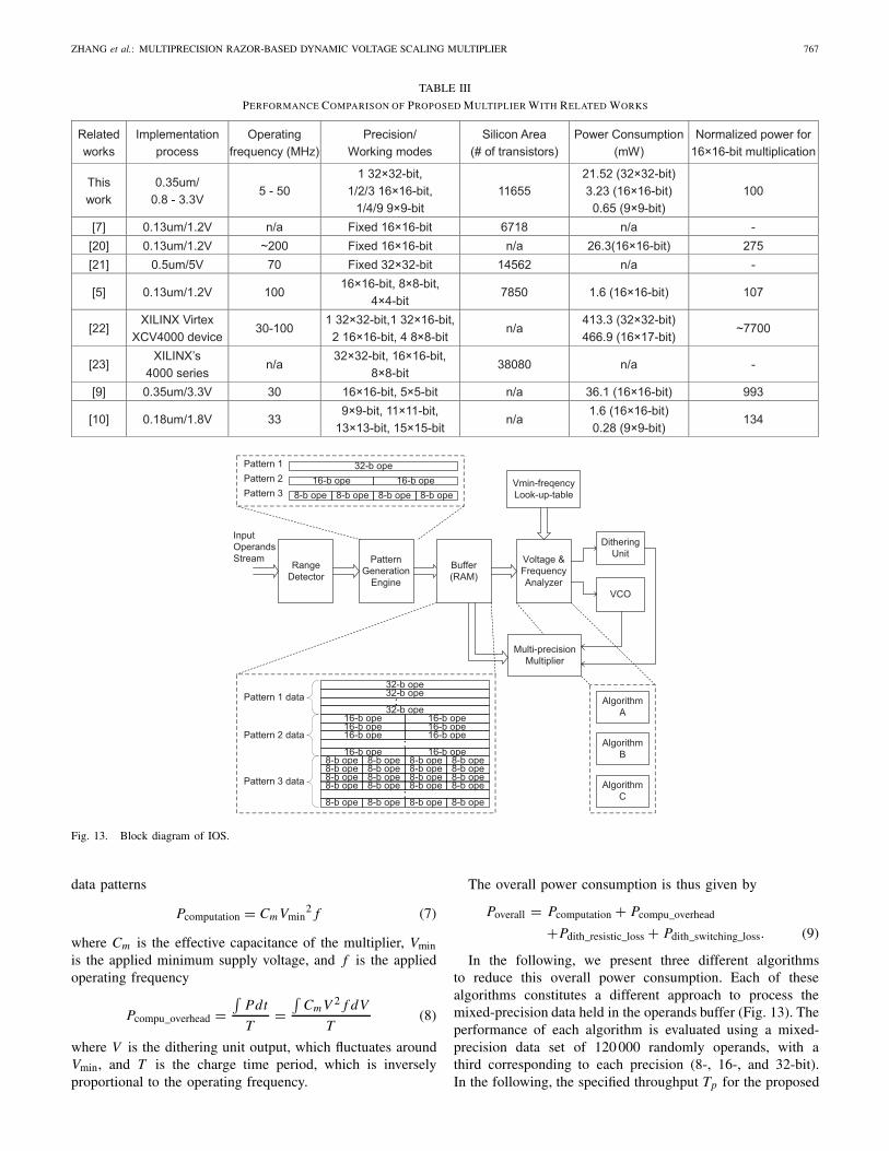
The block diagram of the IOS is shown in Fig. 13. It iscomposed of an operand range detector, a pattern generationengine, a 2 k-bit buffer-(RAM), and a frequency/voltage ana-lyzer. The scheduler operates as follows. The inputs operandsare first sent to the range detector, which classifies themaccording to their precision: 32, 16, or 8-bit. The classifieddata is then grouped by the pattern generation engine, whichpacks same-precision data into three different 32-bit datapatterns (Fig. 13): 1) pattern 1 corresponds to original 32-bitinput operand Data; 2) pattern 2 combines two 16-bit operandsdata (with their redundant 16 MSBs removed); and 3) pattern3 combines four 8-bit operand data (with their redundant24 MSBs removed). At each clock cycle, a 32-bit data patterncan be processed, owning to the PP capability of the proposedmultiplier. This resembles the SIMD structure, and helps to putthe MP and PP capability into real effect. As in Fig. 13, thethree different data patterns are counted (N32, N16, and N8)and stored into a buffer, together with the respective voltagesand clock frequencies at which they should be processed. Foreach full buffer, there will only be two transitions needed:(Vmin8, f8)–(Vmin16, f16), and (Vmin16, f16)–(Vmin32, f32).To limit the silicon area overhead, we chose a 2k-RAM,which can store 60 32-bit data patterns. The voltage/frequencyanalyzer specifies the values of Vmin32, Vmin16, Vmin8, f32, f16,and f8 to the dithering unit and VCO. The Vmin– f pairs aredetermined during the characterization of the chip and storedin the LUT (Fig. 13).
B. Problem Formulation
Given a random mixed-precision (32-, 16-, or 8-bit) inputdata stream and specified throughput Tp , our goal is todetermine the voltages (Vmin32, Vmin16, Vmin8) and frequencies( f32, f16 and f8) at which each precision data group should beprocessed such that the total power consumption is minimized.In the following analysis, we consider the following fourcomponents of the total power consumption: 1) the resis-tive power loss Pdith_resistic_loss of the dithering unit; 2) theswitching power loss Pdith_switching_loss of the dithering unit;3) the dynamic power consumption Pcomputation associated tothe multiplication computation; and 4) finally, Pcompu_overheadthat corresponds to the power consumption of the lattercomputation when carried out at voltage levels higher thanthe nominal Vmin. The equations of the aforementioned fourcomponents of the total power consumption are given below
Pdith_resistic_loss = I 2char Ron (5)
where Ichar is the charge current of the dithering unit, and Ronis the equivalent resistance of the dithering switch
Pdith_switching_loss = Cg Vdd2 f
N(6)
where Cg is the gate capacitance of the dithering switch, Vddis the 3.3 V standard voltage, and N is the number of input
ZHANG et al.: MULTIPRECISION RAZOR-BASED DYNAMIC VOLTAGE SCALING MULTIPLIER 767
TABLE III
PERFORMANCE COMPARISON OF PROPOSED MULTIPLIER WITH RELATED WORKS
Range Detector
Pattern Generation
Engine
Buffer (RAM)
Voltage & Frequency Analyzer
Input Operands Stream
Dithering Unit
VCO
Multi-precisionMultiplier
Vmin-freqencyLook-up-table
8-b ope 8-b ope 8-b ope 8-b ope..
8-b ope 8-b ope 8-b ope 8-b ope8-b ope 8-b ope 8-b ope 8-b ope8-b ope 8-b ope 8-b ope 8-b ope8-b ope 8-b ope 8-b ope 8-b ope
16-b ope 16-b ope..
16-b ope 16-b ope16-b ope 16-b ope16-b ope 16-b ope
32-b ope..
32-b ope32-b ope
Pattern 1 data
Pattern 2 data
Pattern 3 data
8-b ope8-b ope8-b ope 8-b ope16-b ope 16-b ope
32-b opePattern 1Pattern 2Pattern 3
AlgorithmA
AlgorithmB
AlgorithmC
Fig. 13. Block diagram of IOS.
data patterns
Pcomputation = Cm Vmin2 f (7)
where Cm is the effective capacitance of the multiplier, Vminis the applied minimum supply voltage, and f is the appliedoperating frequency
Pcompu_overhead =∫
Pdt
T=
∫Cm V 2 f dV
T(8)
where V is the dithering unit output, which fluctuates aroundVmin, and T is the charge time period, which is inverselyproportional to the operating frequency.
The overall power consumption is thus given by
Poverall = Pcomputation + Pcompu_overhead
+Pdith_resistic_loss + Pdith_switching_loss. (9)
In the following, we present three different algorithmsto reduce this overall power consumption. Each of thesealgorithms constitutes a different approach to process themixed-precision data held in the operands buffer (Fig. 13). Theperformance of each algorithm is evaluated using a mixed-precision data set of 120 000 randomly operands, with athird corresponding to each precision (8-, 16-, and 32-bit).In the following, the specified throughput Tp for the proposed

768 IEEE TRANSACTIONS ON VERY LARGE SCALE INTEGRATION (VLSI) SYSTEMS, VOL. 22, NO. 4, APRIL 2014
Fig. 14. Operation principles of operand scheduling algorithms A, B, and C. Data Block X and Data Block X+1 refer to two-consecutive operand datablocks subsequently stored into the RAM, respectively.
TABLE IV
DETAILED POWER PERFORMANCE OF DIFFERENT SCHEDULING ALGORITHMS
Algorithm P_computation P_compu_overhead P_dith_resistic_loss P_dith_switching_loss P_overall
A 3.034 mW 3.159 mW 0.059 mW 1.715 mW 8.255 mW
B 2.266 mW 2.565 mW 0.084 mW 1.663 mW 6.578 mW
C 1.682 mW 1.843 mW 0.062 mW 0.975 mW 4.561 mW
32 × 32 bit multiplier is 64 F (Mbits/s), where F is themultiplier’s operating frequency.
C. Algorithm A
In the first algorithm, the multiplier throughput Tp = 64 F iskept constant by fixing the operating frequencies ( f32−, f16−,or f8) of each precision-data group (32-, 16-, or 8-bit) to
f32 = F, f16 = F
2, f8 = F
4(10)
where F is the multiplier’s operating frequency. This isbecause the throughput in 8 × 8 bit multiplication mode is fourtimes that of the 32 × 32 bit multiplication mode and doublethat of the 16 × 16 bit multiplication mode, as a result of themultiplier PP. The minimum supply voltage (Vmin32, Vmin16or Vmin8) associated to each operating frequency ( f32, f16or f8) is determined through a Vmin– f LUT. Algorithm Ashows its limitations when 32-bit operands are processedinitially. As shown in Fig. 14, once all N32 operands of the datablock are processed, the supply voltage (Vn) needs to decreaserapidly from point A (Vmin32) to point B (Vmin16) at which allN16 16-bit operands of the data block should be processed.If N16 is too small, most 16-bit operands will be actuallyprocessed in Sections A and B, that is at a voltage possiblymuch higher than the minimal Vmin16 level. Similarly 8-bitoperands of the data block could be processed in Sections Cand D, B-C, or even A-B for the worst case. This contributes to
increasing Pcompu_overhead. The overall power performance ofalgorithm A is shown in Table IV. Compared with the fixed-width 32 × 32 bit standard multiplier (32 × 32 bit modemust be chosen given that a third of operands are 32-bit),77.7% total power reduction is achieved with a total siliconarea overhead of only 11.1%, when considering DVS, razor,RAM, and dedicated circuitry for scheduling algorithm A.
D. Algorithm B
This algorithm removes all transitions of the power supplyvoltage by making Vmin32, Vmin16, and Vmin8 equal and adjust-ing f32, f16, and f8 such that the overall throughput is keptunchanged. We thus need to have the following:
64N32 + 128N16 + 256N8N32f32
+ N16f16
+ N8f8
= 64 F. (11)
From a LUT, we can obtain the Vmin– f relationship asfollows:
Vmin32 = ψ32( f32) (12)
Vmin16 = ψ16( f16) (13)
Vmin8 = ψ8( f8). (14)
As algorithm B keeps the supply voltage constant
ψ32( f32) = ψ16( f16) = ψ8( f8) = V (15)

ZHANG et al.: MULTIPRECISION RAZOR-BASED DYNAMIC VOLTAGE SCALING MULTIPLIER 769
the operating frequencies f32, f16, and f8 can be determinedby using (11) and (15). For example, when F is set to50 MHz, the values for V , f32, f16, and f8 are found tobe 1.35 V, 20 MHz, 25 MHz, and 35 MHz, respectively.The overall power consumption of algorithm B is shown inTable IV. Due to the complete removal of voltage transitions,the Pcompu_overhead is reduced. Simultaneously, because ofholistic planning, the dynamic computation power is alsooptimized to a lower level. Compared with the fixed-width32 × 32 bit standard multiplier, 81.5% power reduction isachieved with a total silicon area overhead of only 11.9%,when considering DVS, razor, RAM, and dedicated circuitryfor scheduling Algorithm B.
E. Algorithm C
Although Algorithm B removes power supply voltage tran-sitions by setting a single-voltage level V, there may bebetter power saving combinations of power supply voltagesand operating frequencies: (Vmin32, f32), (Vmin16, f16), and(Vmin8, f8). The aim of algorithm C is to find such an optimumfor reduced power consumption. To limit complexity, we willonly seek to minimize the dynamic power dissipated as a resultof the computation
P = CV 2 f (16)
= Cm32V 2min32 f32 + Cm16V 2
min16 f16 + Cm8V 2min8 f8 (17)
= χ( f32, f16). (18)
Given that the Vmin– f relationships are known (12)–(14),one could find the minimum of the above equation for thespecified throughput (11). For example, when F is set to50 MHz, the values for (Vmin32, f32), (Vmin16, f16), (Vmin8, f8)are found to be (1.15 V, 15 MHz), (1.30 V, 20 MHz), and(1.75 V, 45 MHz), respectively. The overall power perfor-mance of algorithm C is shown in Table IV. When consid-ering DVS, razor, RAM, and dedicated scheduling circuitry,algorithm B exhibits the least power consumption, with anoverall power reduction of 86.3%, compared with the standard32 × 32 bit fixed-width multiplier. However, it requires twoadditional dithering units to generate all three discrete powersupply levels Vmin32, Vmin16, and Vmin8 and thus removetransitions among these different supply levels. This increasesthe total silicon area overhead to 27.1%. Therefore, algorithmB provides the most attractive tradeoff with 81.5% reductionand a silicon area overheard of just 11.9%.
VIII. CONCLUSION
We proposed a novel MP multiplier architecture featuring,respectively, 28.2% and 15.8% reduction in silicon area andpower consumption compared with its 32 × 32 bit conven-tional fixed-width multiplier counterpart. When integrating thisMP multiplier architecture with an error-tolerant razor-basedDVS approach and the proposed novel operands scheduler,77.7%–86.3% total power reduction was achieved with a totalsilicon area overhead as low as 11.1%. The fabricated chipdemonstrated run-time adaptation to the actual workload byoperating at the minimum supply voltage level and mini-mum clock frequency while meeting throughput requirements.
The proposed novel dedicated operand scheduler rearrangesoperations on input operands, hence to reduce the number oftransitions of the supply voltage and, in turn, minimized theoverall power consumption of the multiplier. The proposed MPrazor-based DVS multiplier provided a solution toward achiev-ing full computational flexibility and low power consumptionfor various general purpose low-power applications.
ACKNOWLEDGMENT
The authors would like to thank Dr. M.K. Law for hiscomments and discussions. We also would like to acknowledgeMr. S.F. Luk for his help with the chip test measurements.
REFERENCES
[1] R. Min, M. Bhardwaj, S.-H. Cho, N. Ickes, E. Shih, A. Sinha, A. Wang,and A. Chandrakasan, “Energy-centric enabling technologies for wire-less sensor networks,” IEEE Wirel. Commun., vol. 9, no. 4, pp. 28–39,Aug. 2002.
[2] M. Bhardwaj, R. Min, and A. Chandrakasan, “Quantifying and enhanc-ing power awareness of VLSI systems,” IEEE Trans. Very Large ScaleIntegr. (VLSI) Syst., vol. 9, no. 6, pp. 757–772, Dec. 2001.
[3] A. Wang and A. Chandrakasan, “Energy-aware architectures for a real-valued FFT implementation,” in Proc. IEEE Int. Symp. Low PowerElectron. Design, Aug. 2003, pp. 360–365.
[4] T. Kuroda, “Low power CMOS digital design for multimedia proces-sors,” in Proc. Int. Conf. VLSI CAD, Oct. 1999, pp. 359–367.
[5] H. Lee, “A power-aware scalable pipelined booth multiplier,” in Proc.IEEE Int. SOC Conf., Sep. 2004, pp. 123–126.
[6] S.-R. Kuang and J.-P. Wang, “Design of power-efficient configurablebooth multiplier,” IEEE Trans. Circuits Syst. I, Reg. Papers, vol. 57,no. 3, pp. 568–580, Mar. 2010.
[7] O. A. Pfander, R. Hacker, and H.-J. Pfleiderer, “A multiplexer-basedconcept for reconfigurable multiplier arrays,” in Proc. Int. Conf. FieldProgram. Logic Appl., vol. 3203. Sep. 2004, pp. 938–942.
[8] F. Carbognani, F. Buergin, N. Felber, H. Kaeslin, and W. Fichtner,“Transmission gates combined with level-restoring CMOS gates reduceglitches in low-power low-frequency multipliers,” IEEE Trans. VeryLarge Scale Integr. (VLSI) Syst., vol. 16, no. 7, pp. 830–836, Jul. 2008.
[9] T. Yamanaka and V. G. Moshnyaga, “Reducing multiplier energy bydata-driven voltage variation,” in Proc. IEEE Int. Symp. Circuits Syst.,May 2004, pp. 285–288.
[10] W. Ling and Y. Savaria, “Variable-precision multiplier for equalizer withadaptive modulation,” in Proc. 47th Midwest Symp. Circuits Syst., vol. 1.Jul. 2004, pp. I-553–I-556.
[11] K.-S. Chong, B.-H. Gwee, and J. S. Chang, “A micropower low-voltagemultiplier with reduced spurious switching,” IEEE Trans. Very LargeScale Integr. (VLSI) Syst., vol. 13, no. 2, pp. 255–265, Feb. 2005.
[12] M. Sjalander, M. Drazdziulis, P. Larsson-Edefors, and H. Eriks-son, “A low-leakage twin-precision multiplier using reconfigurablepower gating,” in Proc. IEEE Int. Symp. Circuits Syst., May 2005,pp. 1654–1657.
[13] S.-R. Kuang and J.-P. Wang, “Design of power-efficient pipelinedtruncated multipliers with various output precision,” IET Comput. DigitalTech., vol. 1, no. 2, pp. 129–136, Mar. 2007.
[14] J. L. Holt and J.-N. Hwang, “Finite precision error analysis of neuralnetwork hardware implementations,” IEEE Trans. Comput., vol. 42,no. 3, pp. 281–290, Mar. 1993.
[15] A. Bermak, D. Martinez, and J.-L. Noullet, “High-density 16/8/4-bitconfigurable multiplier,” Proc. Inst. Electr. Eng. Circuits Devices Syst.,vol. 144, no. 5, pp. 272–276, Oct. 1997.
[16] T. Kuroda, “Low power CMOS digital design for multimedia proces-sors,” in Proc. Int. Conf. VLSI CAD, Oct. 1999, pp. 359–367.
[17] T. D. Burd, T. A. Pering, A. J. Stratakos, and R. W. Brodersen,“A dynamic voltage scaled microprocessor system,” IEEE J. Solid-StateCircuits, vol. 35, no. 11, pp. 1571–1580, Nov. 2000.
[18] T. Kuroda, K. Suzuki, S. Mita, T. Fujita, F. Yamane, F. Sano,A. Chiba, Y. Watanabe, K. Matsuda, T. Maeda, T. Sakurai, andT. Furuyama, “Variable supply-voltage scheme for low-power high-speed CMOS digital design,” IEEE J. Solid-State Circuits, vol. 33, no. 3,pp. 454–462, Mar. 1998.

770 IEEE TRANSACTIONS ON VERY LARGE SCALE INTEGRATION (VLSI) SYSTEMS, VOL. 22, NO. 4, APRIL 2014
[19] M. Nakai, S. Akui, K. Seno, T. Meguro, T. Seki, T. Kondo,A. Hashiguchi, H. Kawahara, K. Kumano, and M. Shimura, “Dynamicvoltage and frequency management for a low-power embedded micro-processor,” IEEE J. Solid-State Circuits, vol. 40, no. 1, pp. 28–35,Jan. 2005.
[20] J.-Y. Kang and J.-L. Gaudiot, “A simple high-speed multiplier designcomputers,” IEEE Trans. Comput., vol. 55, no. 10, pp. 1253–1258,Oct. 2006.
[21] G. Y. Jeong, J. S. Park, and H. C. Kang, “A Study on multiplierarchitecture optimized for 32-bit processor with 3-stage pipeline,” inProc. Int. SoC Design Conf., Oct. 2004, pp. 656–660.
[22] S. Perri, P. Corsonello, M. A. Iachino, M. Lanuzza, and G. Cocorullo,“Variable precision arithmetic circuits for FPGA-based multimediaprocessors,” IEEE Trans. Very Large Scale Integr. (VLSI) Syst., vol. 12,no. 9, pp. 995–999, Sep. 2004.
[23] S. D. Haynes, A. Ferrari, and P. Y. K. Cheung, “Flexible reconfigurablemultiplier blocks suitable for enhancing the architecture of FPGAs,” inProc. IEEE Custom Integr. Circuits, May 1999, pp. 191–194.
[24] S. Das, D. Blaauw, D. Bull, K. Flautner, and R. Aitken, “Addressingdesign margins through error-tolerant circuits,” in Proc. Design Autom.Conf., Jul. 2009, pp. 11–12.
[25] D. Ernst, N. S. Kim, S. Das, S. Pant, R. Rao, T. Pham, C. Ziesler,D. Blaauw, T. Austin, K. Flautner, and T. Mudge, “Razor: A low-powerpipeline based on circuit-level timing speculation,” in Proc. Int. Symp.Microarchit., Dec. 2003, pp. 7–18.
[26] S. Das, D. Roberts, S. Lee, S. Pant, D. Blaauw, T. Austin, T. Mudge, andK. Flautner, “A self-tuning DVS processor using delay-error detectionand correction,” IEEE J. Solid-State Circuits, vol. 41, no. 4, pp. 792–804,Apr. 2006.
[27] S. Das, C. Tokunaga, S. Pant, W.-H. Ma, S. Kalaiselvan, K. Lai,D. M. Bull, and D. T. Blaauw, “RazorII: In situ error detection andcorrection for PVT and SER tolerance,” IEEE J. Solid-State Circuits,vol. 44, no. 1, pp. 32–48, Jan. 2009.
[28] B. Calhoun and A. Chandrakasan, “Ultra-dynamic voltage scaling usingsub-threshold operation and local voltage dithering in 90 nm CMOS,”in IEEE Int. Solid-State Circuits Conf. Dig. Tech. Papers, Feb. 2005,pp. 300–301.
[29] E. D. Kyriakis-Bitzaros and S. Nikolaidis, “Estimation of bit-level tran-sition activity in datapaths based on word-level statistics and conditionalentropy,” IEE Proc. Circuits, Devices Syst., vol. 149, no. 4, pp. 234–240,Aug. 2002.
[30] A. Youssef, M. Anis, and M. Elmasry, “A comparative study betweenstatic and dynamic sleep signal generation techniques for leakagetolerant designs,” IEEE Trans. Very Large Scale Integr. (VLSI) Syst.,vol. 16, no. 9, pp. 1114–1126, Sep. 2008.
Xiaoxiao Zhang (S’06) received the B.S. degreefrom the Department of Microelectronics, TianjinUniversity, Tianjin, China, and the M.E. degree fromthe Institute of Microelectronics, Chinese Academyof Sciences, Beijing, China, in 2003 and 2006,respectively. She is currently pursuing the Ph.D.degree with the Electronic and Computer Engineer-ing Department, Hong Kong University of Scienceand Technology, Hong Kong. Her Ph.D. researchwork involves the design of low-power real-timedigital image processing (DIP) cores or modules for
a camera-on-a-chip.Her current research interests include low-power and high-performance
VLSI circuits design, signal processing architectures, face detection, and 3-Dobject/face recognition.
Farid Boussaid (M’00–SM’04) received the M.S.and Ph.D. degrees in microelectronics from theNational Institute of Applied Science (INSA),Toulouse, France, in 1996 and 1999, respectively.
He joined Edith Cowan University, Perth, Aus-tralia, as a Postdoctoral Research Fellow, anda member of the Visual Information ProcessingResearch Group in 2000. He joined the Universityof Western Australia, Crawley, Australia, in 2005,where he is currently an Associate Professor.
His current research interests include smart CMOSvision sensors, gas sensors, neuromorphic systems, device simulation, mod-eling, and characterization in deep submicron CMOS processes.
Amine Bermak (M’99–SM’04–F’13) received theM.Eng. and Ph.D. degrees in electronic engineeringfrom Paul Sabatier University, Toulouse, France, in1994 and 1998, respectively.
He joined the Advanced Computer ArchitectureResearch Group, York University, York, U.K., wherehe was working as a Post-Doctoral Fellow onVLSI implementation of CMM neural network forvision applications in a project funded by BritishAerospace. He joined Edith Cowan University,Perth, Australia, in 1998, first as a Research Fellow
working on smart vision sensors, then as a Lecturer and a Senior Lecturer.He is currently a Professor with the Electronic and Computer EngineeringDepartment, Hong Kong University of Science and Technology (HKUST),Hong Kong. His current research interests include VLSI circuits and systemsfor signal, image processing, sensors, and microsystems applications.
Dr. Bermak was a recipient of many distinguished awards, including the2004 “IEEE Chester Sall Award,” the HKUST “Engineering School TeachingExcellence Award” in 2004 and 2009, and the “Best Paper Award” at the 2005International Workshop on System-On-Chip for Real-Time Applications.