Highly Efficient Inorganic-Organic Heterojunction … Efficient Inorganic-Organic Heterojunction...
5
S1 Supplementary Information Highly Efficient Inorganic-Organic Heterojunction Solar Cells Based on SnS-sensitized Spherical TiO 2 Electrodes Wei Guo, Yihua Shen, Mingxing Wu and Tingli Ma* 5 State Key Laboratory of Fine Chemicals, School of Chemical Engineering, Environmental and Biological Science and Technology, Dalian University of Technology, Dalian, 116024, P. R. China *E-mail: [email protected] Experimental Details Synthesis of spherical TiO 2 powders and films 10 Preparation of spherical TiO 2 was performed in the presence of hexadecylamine (HDA), as structure-directing agent, via a sol-gel method, followed by a solvothermal treatment. The solution composition of HDA: H 2 O: KCl: ethanol: TTIP (molar ratio) was varied, in the range of 0.33:3:5.5×10 -3 :236.5:1.0. The detailed process is described in the reference. [1] Synthesis of nanocrystalline TiO 2 powders Nanocrystalline TiO 2 particles were synthesized by hydrothermal methods. [2] Briefly, titanium alkoxide solution (TTIP (titanium iso-propoxide): acetic 15 acid=1:1 (molar ratio)) was poured into deionized water under vigorous stirring at room temperature. After peptization, the resultant mixture was treated in a titanium autoclave at 250 o C for 12 h. Finally, the resultant colloidal solution was concentrated and centrifuged to produce a white precipitate of TiO 2 particle. Preparation of ordered mesoporous TiO 2 films Well-ordered mesoporous TiO 2 films were prepared via a supramolecular-templated route and a subsequent layer-by-layer deposition. [3] Triblock 20 copolymer Pluronic F127 was used as structure-directing agent. The precursor solution was composed of TTIP: AcAc: HCl: H 2 O/ethanol: F127. Then, the solution was deposited on FTO glass by spin coating. The films were sintered to remove organic solvent and to improve the nanocrystallinity of the mesoporous TiO 2 . The thickness of the well ordered TiO 2 films was ca. 5 μm. Fabrication of TiO 2 electrodes To prepare the electrodes, parts of the conductive layer on the FTO glass were first etched using zinc powder and hydrochloric acid. Then, the FTO was 25 washed and sonicated in ethanol and acetone. A dense TiO 2 layer was spin coated on the conductive layer using TiO 2 organic sol and sintered at 450 o C for 2 h. [4] TiO 2 powder were dispersed in the solution of terpineol and ethyl cellulose to form viscous paste. Then, the paste was coated on the pre- patterned FTO glass using a doctor-blade method. The films were sintered at 500 o C for 30 min in air. Next, the films were soaked in 40 mM TiCl 4 at 70 o C for 30 min, and then sintered again at 500 o C for 30 min in air. The thickness of the films was controlled to be ca. 8 μm. SnS deposition 30 SnS-sensitized TiO 2 films were prepared by a modified chemical bath deposition (CBD). [5] Considering the wetting properties of TiO 2 films, we adjusted the solvent of the CBD solution, from pure water to a mixed solution of ethanol and deionized water. The SnS CBD solution was composed of 1.13g SnCl 2 dissolved in 5 mL acetone, 8 mL of 98% triethanolamine, 8 mL thioacetamide, and 6 mL 25%-28% ammonia solution. The total volume of the solution was adjusted to 100 mL using a mixed solution of ethanol and deionized water (v/v, 2:8). For the SnS deposition, the TiO 2 films were placed in the CBD solution at 75 o C for varying times. 35 Solar cell fabrication Poly(3-hexylthiophene) (P3HT, Sigma Aldrich, 15 mg/mL in chlorobenzene) was spin coated on TiO 2 -SnS films at 2500 rpm for 60 s and dried on a hot plate at 110 o C for 10 min. Then, a poly (3-4-ethylenedioxythiophene) doped with poly (4-stylenesulfonate) (PEDOT: PSS, Sigma Aldrich) was spin coated twice on TiO 2 -SnS-P3HT films at 2500 rpm for 60 s, and then dried at 110 o C for 10 min. Silver paste was coated on the top of a TiO 2 -SnS-P3HT- PEDOT: PSS film using a doctor-blade method and dried at 100 o C for 10 min. To completely remove the solvent, the devices were annealed at 90 o C for 40 2 h in a vacuum oven. The active area of the devices was 0.12 cm 2 . A mask made of black tape, with an area of 0.04 cm 2 , was used to define the illumination area of the devices. Characterization. The phase compositions of TiO 2 and SnS were determined using X-ray diffraction analysis (XRD, D/MAX-2400) with Cu Kα radiation (γ=0.154 nm). Microstructures of spherical TiO 2 films were studied using field-emission scanning electron microscopy (FE-SEM S-4800, Hitachi). An automatic 45 adsorption apparatus (Belsorp 18-plus) was used to analyze the surface areas of TiO 2 films by Brunauer-Emmett-Teller (BET) method. The UV-Vis reflection spectra were measured using a spectrophotometer (JASCO V-570). Current-voltage curves of HSCs were obtained at ambient conditions by applying an external bias to the cells and measuring the generated photocurrent under white light irradiation using a digital source meter (Keithley 2601) and a solar simulator (100 mW/cm 2 , PEC-L15). Photon flux was determined using a power meter (Nova, Ophir Optronics Ltd.) and a calibration cell (BS- 520, s/n 019, Bunkoh-Keiki Co., Ltd.). The electron lifetime (τ) and charge extraction measurement were performed using the SLIM-PCV (PSL-100, 50 EKO) with stepped laser beam. The Fermi level potential of SnS/TiO 2 and TiO 2 films were analyzed using an impedance spectrum analyzer (Zahner IM6e) along with the Mott-Schottky equation, [6] i.e. 1 C 2 = 2 e¦Å ¦Å 0 N D E-E F - kT e where C represents the capacitance of the space charge region, ε 0 the vacuum permittivity, ε the dielectric constant of the TiO 2 layer, e the electron charge, E the applied potential, E F the Fermi level potential, k the Boltzmann constant, T the absolute temperature, and N D the donor density. The temperature term 55 is generally small and can be neglected. In this work, measurements were performed by applying a sinusoidal potential perturbation with a small Electronic Supplementary Material (ESI) for Chemical Communications This journal is © The Royal Society of Chemistry 2012
-
Upload
hoangkhanh -
Category
Documents
-
view
227 -
download
0
Transcript of Highly Efficient Inorganic-Organic Heterojunction … Efficient Inorganic-Organic Heterojunction...

S1
Supplementary Information
Highly Efficient Inorganic-Organic Heterojunction Solar Cells Based on SnS-sensitized Spherical TiO2 Electrodes
Wei Guo, Yihua Shen, Mingxing Wu and Tingli Ma* 5
State Key Laboratory of Fine Chemicals, School of Chemical Engineering, Environmental and Biological Science and Technology, Dalian University of
Technology, Dalian, 116024, P. R. China
*E-mail: [email protected]
Experimental Details
Synthesis of spherical TiO2 powders and films 10
Preparation of spherical TiO2 was performed in the presence of hexadecylamine (HDA), as structure-directing agent, via a sol-gel method, followed by a solvothermal treatment. The solution composition of HDA: H2O: KCl: ethanol: TTIP (molar ratio) was varied, in the range of 0.33:3:5.5×10⁻³:236.5:1.0. The detailed process is described in the reference.[1]
Synthesis of nanocrystalline TiO2 powders Nanocrystalline TiO2 particles were synthesized by hydrothermal methods.[2] Briefly, titanium alkoxide solution (TTIP (titanium iso-propoxide): acetic 15
acid=1:1 (molar ratio)) was poured into deionized water under vigorous stirring at room temperature. After peptization, the resultant mixture was treated in a titanium autoclave at 250 oC for 12 h. Finally, the resultant colloidal solution was concentrated and centrifuged to produce a white precipitate of TiO2 particle. Preparation of ordered mesoporous TiO2 films
Well-ordered mesoporous TiO2 films were prepared via a supramolecular-templated route and a subsequent layer-by-layer deposition.[3] Triblock 20
copolymer Pluronic F127 was used as structure-directing agent. The precursor solution was composed of TTIP: AcAc: HCl: H2O/ethanol: F127. Then, the solution was deposited on FTO glass by spin coating. The films were sintered to remove organic solvent and to improve the nanocrystallinity of the mesoporous TiO2. The thickness of the well ordered TiO2 films was ca. 5 μm. Fabrication of TiO2 electrodes
To prepare the electrodes, parts of the conductive layer on the FTO glass were first etched using zinc powder and hydrochloric acid. Then, the FTO was 25
washed and sonicated in ethanol and acetone. A dense TiO2 layer was spin coated on the conductive layer using TiO2 organic sol and sintered at 450 oC for 2 h.[4] TiO2 powder were dispersed in the solution of terpineol and ethyl cellulose to form viscous paste. Then, the paste was coated on the pre-patterned FTO glass using a doctor-blade method. The films were sintered at 500 oC for 30 min in air. Next, the films were soaked in 40 mM TiCl4 at 70 oC for 30 min, and then sintered again at 500 oC for 30 min in air. The thickness of the films was controlled to be ca. 8 μm. SnS deposition 30
SnS-sensitized TiO2 films were prepared by a modified chemical bath deposition (CBD).[5] Considering the wetting properties of TiO2 films, we adjusted the solvent of the CBD solution, from pure water to a mixed solution of ethanol and deionized water. The SnS CBD solution was composed of 1.13g SnCl2 dissolved in 5 mL acetone, 8 mL of 98% triethanolamine, 8 mL thioacetamide, and 6 mL 25%-28% ammonia solution. The total volume of the solution was adjusted to 100 mL using a mixed solution of ethanol and deionized water (v/v, 2:8). For the SnS deposition, the TiO2 films were placed in the CBD solution at 75 oC for varying times. 35
Solar cell fabrication Poly(3-hexylthiophene) (P3HT, Sigma Aldrich, 15 mg/mL in chlorobenzene) was spin coated on TiO2-SnS films at 2500 rpm for 60 s and dried on a
hot plate at 110 oC for 10 min. Then, a poly (3-4-ethylenedioxythiophene) doped with poly (4-stylenesulfonate) (PEDOT: PSS, Sigma Aldrich) was spin coated twice on TiO2-SnS-P3HT films at 2500 rpm for 60 s, and then dried at 110 oC for 10 min. Silver paste was coated on the top of a TiO2-SnS-P3HT-PEDOT: PSS film using a doctor-blade method and dried at 100 oC for 10 min. To completely remove the solvent, the devices were annealed at 90 oC for 40
2 h in a vacuum oven. The active area of the devices was 0.12 cm2. A mask made of black tape, with an area of 0.04 cm2, was used to define the illumination area of the devices. Characterization.
The phase compositions of TiO2 and SnS were determined using X-ray diffraction analysis (XRD, D/MAX-2400) with Cu Kα radiation (γ=0.154 nm).
Microstructures of spherical TiO2 films were studied using field-emission scanning electron microscopy (FE-SEM S-4800, Hitachi). An automatic 45
adsorption apparatus (Belsorp 18-plus) was used to analyze the surface areas of TiO2 films by Brunauer-Emmett-Teller (BET) method. The UV-Vis
reflection spectra were measured using a spectrophotometer (JASCO V-570). Current-voltage curves of HSCs were obtained at ambient conditions by
applying an external bias to the cells and measuring the generated photocurrent under white light irradiation using a digital source meter (Keithley 2601)
and a solar simulator (100 mW/cm2, PEC-L15). Photon flux was determined using a power meter (Nova, Ophir Optronics Ltd.) and a calibration cell (BS-
520, s/n 019, Bunkoh-Keiki Co., Ltd.). The electron lifetime (τ) and charge extraction measurement were performed using the SLIM-PCV (PSL-100, 50
EKO) with stepped laser beam. The Fermi level potential of SnS/TiO2 and TiO2 films were analyzed using an impedance spectrum analyzer (Zahner
IM6e) along with the Mott-Schottky equation,[6] i.e.
1C2 =
2
e¦Å¦Å0ND
E-EF-kTe
where C represents the capacitance of the space charge region, ε0 the vacuum permittivity, ε the dielectric constant of the TiO2 layer, e the electron charge, E the applied potential, EF the Fermi level potential, k the Boltzmann constant, T the absolute temperature, and ND the donor density. The temperature term 55
is generally small and can be neglected. In this work, measurements were performed by applying a sinusoidal potential perturbation with a small
Electronic Supplementary Material (ESI) for Chemical CommunicationsThis journal is © The Royal Society of Chemistry 2012
S2
amplitude (10 mV), superimposed on a fixed dc potential, varying within appropriate potential windows from -0.6 to 0 V (vs. Ag/AgCl) in PBS buffer solution (10 mM Na2HPO4/KH2PO4; 2 mM K3PO4; 137 mM NaCl; 2.7 mM KCl, pH 7.4-7.6; Shanghai Sangon Biological Engineering Technology & Service Co., Ltd.). The TiO2 films used for this analysis had a film thickness of ca. 6 μm.
References
[1] Y. B. Cheng, D. H. Chen, L. Cao, F. Z. Huang, P. Imperia and R. A. Caruso, J Am. Chem. Soc. 2010, 132, 4438. 5
[2] S. Ito, T. N. Murakami, P. Comte, P. Liska, C. Grätzel, M. K. Nazeeruddin and M. Grätzel, Thin Solid Films, 2008, 516, 4613. [3] Y. Zhang, Z. Xie and J. Wang, ACS Appl Mater Interfaces, 2009, 1, 2789. [4] S. Q. Zhang, H. Yu, H. J. Zhao, G. Will and P. R. Liu, Electrochim Acta 2009, 54, 1319. [5] H. Gong, Y. Wang, B. H. Fan and G. X. Hu, J Phys. Chem. C 2010, 114, 3256. [6] F. Fabregat-Santiago, G. Garcia-Belmonte, J. Bisquert, P. Bogdanoff and A. Zaban, J Electrochem Soc, 2003, 150, E293. 10
Electronic Supplementary Material (ESI) for Chemical CommunicationsThis journal is © The Royal Society of Chemistry 2012

S3
Figure S1. XRD patterns of TiO2 powder (a) and SnS (b) deposited in chemical bath at 80 oC for 3 h.
5
Figure S2. SEM images of the cross section of SnS-HSCs (a) and plane section of TiO2-SnS-P3HT (b).
Figure S3. EDX spectra. (a) SnS-TiO2 film; (b) SnS-sensitized a single TiO2 sphere; (c) Cross-section of TiO2-SnS-P3HT-Ag HSCs, Ti (red), Sn (bule), S (green).
10
(b)(a)
a
10 μm
b
10 μm
c
10 μm
Electronic Supplementary Material (ESI) for Chemical CommunicationsThis journal is © The Royal Society of Chemistry 2012
S4
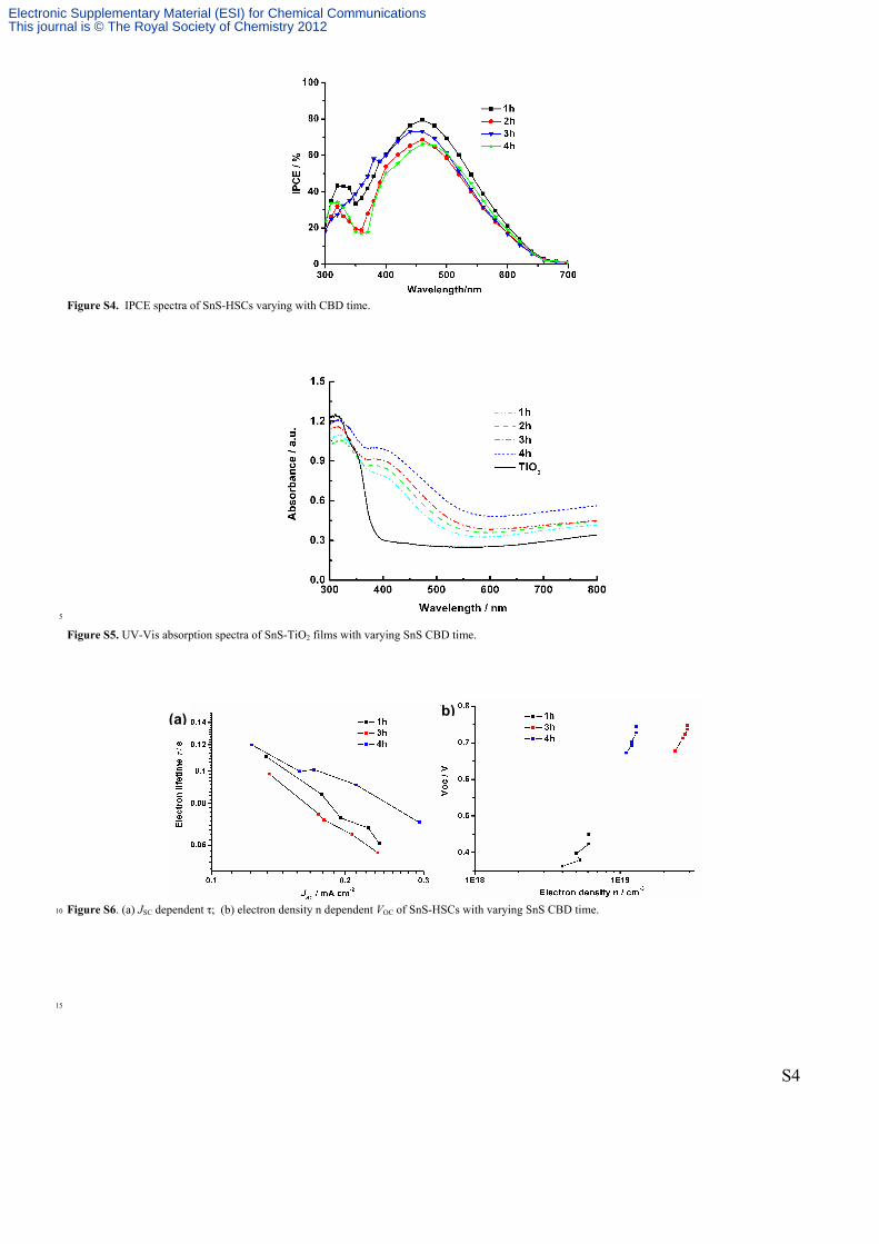
Figure S4. IPCE spectra of SnS-HSCs varying with CBD time.
5
Figure S5. UV-Vis absorption spectra of SnS-TiO2 films with varying SnS CBD time.
Figure S6. (a) JSC dependent τ; (b) electron density n dependent VOC of SnS-HSCs with varying SnS CBD time. 10
15
(b)(a)
Electronic Supplementary Material (ESI) for Chemical CommunicationsThis journal is © The Royal Society of Chemistry 2012

S5
Figure S7. Mott-Schottky curves of TiO2 and TiO2-SnS films. The thickness of TiO2 films were ca. 6 μm.
5
Figure S8. SEM images of SnS-sensitized nc-TiO2 films varying with CBD time. (a) 0h; (b) 1h; (c) 2h; (d) 3h; (e) 4h, scale bar 200 nm; (f) SnS-sensitized spherical TiO2 films with the CBD time 3h, scale bar 10 μm.
Electronic Supplementary Material (ESI) for Chemical CommunicationsThis journal is © The Royal Society of Chemistry 2012