Higher Routability and Reduced Crosstalk Noise by...
14
Transcript of Higher Routability and Reduced Crosstalk Noise by...

Transactions D:Computer Science & Engineering andElectrical EngineeringVol. 17, No. 1, pp. 11{24c Sharif University of Technology, June 2010
Higher Routability and ReducedCrosstalk Noise by Asynchronous
Multiplexing of On-Chip Interconnects
A. Jahanian1 and M. Saheb Zamani2;�
Abstract. The signal integrity problem, especially crosstalk noise, is an important issue in physicaldesign in the nanometer regime. Wire multiplexing is a recently proposed method to reduce these problemsin current design methodologies. This technique is presented to increase the routability of the designand also reduce crosstalk noise by serializing parallel wires via delay insensitive asynchronous serialtransceivers. In this paper, this technique is improved in terms of routability and computation time and,also, its impact on crosstalk is examined. Finally, it is evaluated with 180 nm and 130 nm technologies.Experimental results show that for the attempted benchmarks, congestion and routability are improved by15.54% and 21.57% on average, respectively, and crosstalk noise is improved by 9.51% on average. Theseimprovements are achieved at the cost of a slight increase in power consumption (0.12% on average) andruntime (less than 10.01% on average).
Keywords: Asynchronous serial transmission; Crosstalk; Routability.
INTRODUCTION
Signal integrity is an important metric for the qualityof a design and it has become dominant for large andcomplicated designs. In a congested design, many wireshave to be detoured at the global routing stage anda large number of long wires are generated. Theseglobal wires can have a great impact on the routabilityand performance of the design and may also result incrosstalk and manufacturability problems. Therefore,congestion and crosstalk noise reduction have a keyrole in the performance, manufacturability and signalintegrity of designs.
Routing congestion (or congestion) of a layoutrectangular region (bin) is de�ned as the number ofused routing tracks divided by the total number ofrouting tracks on the perimeter of the bin. If thecongestion of a bin goes beyond 100%, those internal
1. Department of Electrical and Computer Engineering, ShahidBeheshti University, G.C., Tehran, P.O. Box 19839-63113,Iran.
2. Department of Information Technology and Computer Engi-neering, Amirkabir University of Technology, Tehran, P.O.Box 15875-4413, Iran.
*. Corresponding author. E-mail: [email protected]
Received 11 October 2009; received in revised form 14 December2009; accepted 29 December 2009
nets of the bin, which should be connected out, arenot routable. In this situation, the design is notroutable. Therefore, routing congestion and routabilityare dependent concepts.
Asynchronous serial transceivers can be usedto improve congestion and routability in applicationspeci�c integrated circuit design methodology. Withthe emergence of the globally asynchronous locallysynchronous concept [1], some techniques for usingasynchronous serial transceivers in Network-On-Chip(NOC) systems have been proposed [2]. These systemswere mainly used to improve the data transmissiondelay between cores. Conventional asynchronous cir-cuits used di�erential-signaling serial links that madethem inappropriate for on-chip applications. Thisis because they require PLL-based clock and datarecovery circuits, which consume excessive power andarea [3].
In [4], an NOC with a new serialization mecha-nism was proposed, which provides high performanceserialization with small overhead. In this approach, thedata transmission bandwidth is automatically adjustedbased on the workload of the network. This methodwas implemented and tested in 0.18 �m technology at3 Gb/s.
In [5], the authors proposed a serial linktransceiver for global on-chip communications, working

12 A. Jahanian and M. Saheb Zamani
at 3 Gb/s per wire in a standard 0.18 �m CMOSprocess, with low crosstalk-induced delay variability.They implemented a pure electrical link without anyrepeater in higher layers of metals.
Tei e and Manohar [6] presented a high-speedand clockless serial link transceiver for inter-chip com-munication. Their experiments showed that theirtransceiver operates at up to 3 Gb/s in 0.18 �m CMOStechnology.
Dobkin et al. [7-9] presented a novel bit-serialinterconnect structure with a new data encoding styleto encode each bit in one transition in a pipelinedstructure. They showed that their asynchronous circuitcan send or receive a new bit at a data cycle of a singleFO4 (i.e. fan-out of 4) inverter delay.
The authors of this paper present a new approachfor serializing the parallel wires using an asynchronousserial transceiver to improve routing congestion andthe crosstalk noise of designs [10]. This mechanismwas called metro-on-chip (MOC) because its semanticis similar to metro transportation systems in large citiesthat convey many passengers in one trip. In thismethodology, non-critical and su�ciently long wiresare selected and serialized at the signal sources andthen, they are demultiplexed into parallel signals atthe destinations after serial transmission. Finally,these demultiplexed signals travel to their sinks. Itis worthwhile to note that a congestion metric isa good metric, which can be more useful if it ismeasured in terms of routability. This paper has twomajor improvements compared with [10]. The �rst isthat in [10] no results were reported in terms of theroutability of the design after MOC insertion. Due toimportance of routability in modern complicated chips,routability analysis is very crucial for any proposedmethodology in the physical design era.
It is noted that test coverage of multiplexed wiresis lower than for parallel ones, because inserting afault on multiplexed wire means that any of all themultiplexed lines may actually become stuck at thatvalue.
In this paper, we improve the metro-on-chipmechanism in terms of routability and computationtime and also examine its impact on crosstalk with anewer technology feature size.
OVERVIEW ON THE METRO-ON-CHIP
Metro-on-Chip ConceptIn the conventional physical design ow, terminals ofeach net are connected via dedicated and specializedwires (Figure 1).
However, in new circuits which have a large num-ber of nets, routing congestion raised issues in terms ofroutability, signal integrity and even the performance ofthe design. Multiplexing the nets in congested circuits
Figure 1. Conventional dedicated wires.
Figure 2. Serial multiplexed wires.
can be an e�ective technique to reduce congestion andimprove routability. The main concept of this paper isto automatically �nd non-critical and su�ciently longwires and multiplex, and send them using asynchronousserial transmission hardware. This idea is similar tothe metro system in large cities, which conveys manypassengers in one trip to reduce tra�c congestion. Inthis paper, a static paradigm of the metro is imple-mented in which the metro has �xed stations at thesource and the destination without any intermediatestations (Figure 2).
Inserting the MOC cells (MOC multiplexers anddemultiplexers) after detail or even global routing canimpose large costs due to the need for updating therouting or placement results. On the other hand, MOCinsertion at the earlier stages of physical design (e.g.partitioning or oorplanning) may not be e�ective be-cause, at those stages, there is not enough informationabout cell locations and, therefore, the estimations ofphysical parameters may be very rough. In this paper,MOC modules are inserted after detailed placementwhere the locations of cells and white spaces have beendetermined.
The contributions of this approach are in de-creasing routing congestion and total wirelength andalso in increasing design routability by reducing thenumber of global nets. It should be noted thatcongestion reduction does not increase the performanceof the design explicitly, but it may improve the timingcharacteristics by avoiding the detoured global netsresulted from routing congestion.
FAST SERIAL TRANSCEIVER
The fast serial communication mechanism proposedin [7] is used as the serial link hardware. The area,

Improved Routability and Crosstalk by Wire Multiplexing 13
delay and other characteristics of this system play a keyrole in the feasibility and quality of the proposed EDAdesign ow. In the following subsection, the hardwarestructure and transmission delay of this module havebeen brie y reviewed.
Serial Transmission System Review
The fast serial link transceiver [7] uses low-latencysynchronizers at the sources and sinks with a two-phasenon-return and a zero level encoded dual rails (LEDR)asynchronous protocol that allows non-uniform delayintervals between successive bits. Acknowledgment oftransmission is returned only once per word, ratherthan bit by bit. This enables multiple bits to betransmitted in a wave-pipelined manner over the serialchannel. The main structure of this mechanism isshown in Figure 3.
In [7], a high data rate shift-register structurefor an asynchronous serializer and deserializer hasbeen proposed. It operates at about one fan-out 4inverter (FO4) delay and can be fully implemented inCMOS technology without any requirement to PLL orauxiliary clock generation circuitry.
Let MOC cluster, i, consist of mi wires. The serialtransmission hardware of this cluster contains a mi-bitshift-register in the MUX module and also a mi-bit
Figure 3. Fast bit-serial transmission scheme.
shift-register in the DEMUX module. The total delayof MOC cluster, i, consists of �ve elements:
� Delay of wires from source nodes to the MUX inputpins (input wires),
� Delay of multiplexing shift registers,� Delay of transmission line from MUXes to DE-
MUXes,� Delay of demultiplexing shift registers,� Delay of wires from the DEMUX output pins to sink
nodes (output wires).
In Figure 4, the �ve sub-elements of MOC delayare shown.
With a good clustering algorithm, source/sinknodes are close to the source/sink gravity centersand the delays of input/output wires are very small.Because of the pipeline structure of the serial linktransceiver proposed in [7], each input signal can beapplied to the MUX input while the previous signal isbeing multiplexed (except for the �rst input). More-over, each output signal can be applied to its sink whilethe next signal is being demultiplexed (except for thelast output). Therefore, total delay of the ith MOCcluster with mi wires can be calculated as:
D(i) = ID(i; 1) + 2:mi:max(DFO4; TD(i))
+OD(i;mi); (1)
where ID(i; 1) is the delay of the �rst input signal,OD(i;mi) is the delay of the last output, TD(i) isthe transmission line delay in ith cluster and DFO4represents an FO4 inverter delay. The �rst term in thisequation is the delay of wires from source nodes to theMUX input pins. Because of overlapping the delay ofshifting and transmission operations, the second termis maximum between the delay of one-bit shift register(DFO4) and the transmission delay of one bit (TD(i)).Finally, the last term shows the delay of wires from theDEMUX output pins to sink nodes.
Figure 4. Delay sub-elements of cluster i.
14 A. Jahanian and M. Saheb Zamani
Interfacing the MOC System in a GeneralDesign
Inserting an asynchronous module in a synchronouscircuit may change the functionality of the wholesystem due to the violation of the setup and hold timerequirements of synchronous registers. In this section,a feasible solution for interfacing the asynchronoustransmission module and a synchronous circuit with aglobal clock is presented. In the proposed interface, oneach rising edge of the system clock, the asynchronousserial link starts to convey a copy of signals at thesource toward the destination and this operation isrepeated for all input signals. At the end of the op-eration, a word-acknowledge signal is returned back tothe sender. The process of serializing, transmission anddeserializing is initiated by the activation of the startsignal and the completion of the whole transmissionprocess is indicated by `1' on word ack signal. Thesignaling of the synchronous system after inserting theasynchronous serial link is shown in Figure 5.
In this mechanism, the clock period must beextended by the delay of MOC hardware if the pathscontaining the multiplexed wires do not have enoughdelay slack (i.e. their delays are close to the maximumclock period of the design). However, if the pathsof the selected wires have enough delay slack, themultiplexing delay will not a�ect the critical path ofthe design. Therefore, the criticality of nets must betaken into account for inserting the MOC cells andmultiplexing the wires. In our approach, only the wireswhich do not violate the design timing constraints afterMOC insertion are chosen to be multiplexed.
MOC-BASED PHYSICAL DESIGN FLOW
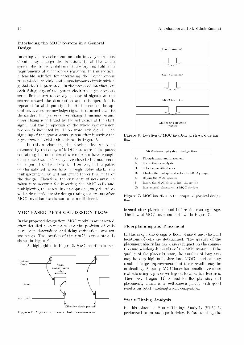
In the proposed design ow, MOC modules are insertedafter detailed placement where the position of cellshave been determined and delay estimations are nottoo rough. The location of the MoC insertion stage isshown in Figure 6.
As highlighted in Figure 6, MoC insertion is per-
Figure 5. Signaling of serial link transmission.
Figure 6. Location of MOC insertion in physical design ow.
Figure 7. MOC insertion in the proposed physical design ow.
formed after placement and before the routing stage.The ow of MOC insertion is shown in Figure 7.
Floorplanning and Placement
In this stage, the design is oor-planned and the �nallocations of cells are determined. The quality of theplacement algorithm has a great impact on the conges-tion and wirelength bene�ts of the MOC system. If thequality of the placer is poor, the number of long netsmay be very high and, therefore, MOC insertion mayresult in large improvement; but these results may bemisleading. Actually, MOC insertion bene�ts are morerealistic using a placer with good localization features.Therefore, Dragon [11] is used for oorplanning andplacement, which is a well-known placer with goodresults on total wirelength and congestion.
Static Timing Analysis
In this phase, a Static Timing Analysis (STA) isperformed to estimate path delay. Before routing, the

Improved Routability and Crosstalk by Wire Multiplexing 15
topologies of nets have not been determined and theymust be estimated for static timing analysis.
A Re�ned Single Trunk Steiner Tree (RSTST)model [12] is used to predict the topologies of netsbefore the routing stage. After estimating the topologyof nets, the delay of each path in the design is calculatedusing the Elmore delay model and the critical paths ofthe design are determined. A critical path list will beused to select non-critical nets for multiplexing.
Select Non-Critical Nets
In this stage, a list of non-critical and su�ciently longwires is generated based on the results of the statictiming analysis. After STA, a list of paths whose delaysare greater than a speci�ed threshold (Td) has beengenerated. These nets cannot be multiplexed becausethey may violate the timing constraints of the design.Therefore, these nets are marked to be excluded fromMOC groups.
The appropriate value for Td has an importante�ect on the bene�ts of MOCs. In this subsection, anapproximation technique to set its value is presented.Td can be speci�ed as:
Td = Tw � �:Tw; (2)
where Tw is the most critical delay of the design (timingwall) and � is a number between 0 and 1, which de�nesa margin for near critical nets. In other words, thedelay overhead of each MOC cluster must be less than�. Tw. Therefore, all paths whose delays are greaterthan Td are considered as critical paths and their netsare not selected for multiplexing. Td must be adjusted
by trial and error if no appropriate prediction could bemade. However, an appropriate value is estimated forit based on the following analysis.
Consider cluster gi with mi nets. If the sourcesand sinks in gi are su�ciently close to the MUX andthe DEMUX, respectively, the total delay of gi canbe approximated as 2.mi:DFO4 in which DFO4 is oneFO4 inverter delay. By this assumption, the followingcondition must be met to avoid any performancedegradation in the design:
Di � �:Tw ) mi � �:Tw2:DFO4
: (3)
This equation shows the relation of average MOCcluster size and the delay threshold of the design. Weused this approximation for choosing the value of � andcluster sizes. Table 1 shows the experimental results ofthis approximation.
In Table 1, Approximated cluster size shows theapproximated values for cluster sizes, Actual clustersize shows the best found values for cluster sizes at theend of the test process, and column Error representsthe absolute percentage of di�erences between approx-imated and actual cluster sizes. This table showsthat the error of this approximation is small (7.01 onaverage) and Equation 3 can be used as a good initialapproximation for mi.
Cluster the Multiplexed Nets into MOCGroups
In this phase, the selected nets are clustered into somegroups such that the nets in each group have close
Table 1. Approximated and actual cluster sizes.
Index Circuit TW(ps)
ApproximatedCluster Size
ActualCluster
Size
Error(%)
1 spi 2524.24 0 0 0
2 tv80 4163.09 0 0 0
3 pci bridge32 18727.58 31.21263 23.4 7.812
4 dma 18491.70 30.8195 24.5 6.319
5 b20 1 6961.51 11.60252 10.21 0.607
6 b22 10796.53 17.99422 18.75 0.755
7 b22 1 10233.41 17.05568 24.3 7.244
8 wb conmax 8816.92 0 0 0
9 b17 27207.41 45.34568 26.55 18.795
10 b17 1 27291.20 45.48533 36.86 8.625
11 Ethernet 23330.71 38.88452 30.05 8.834
12 b18 73038.43 121.7307 96.7 25.03
Average 7.01
16 A. Jahanian and M. Saheb Zamani
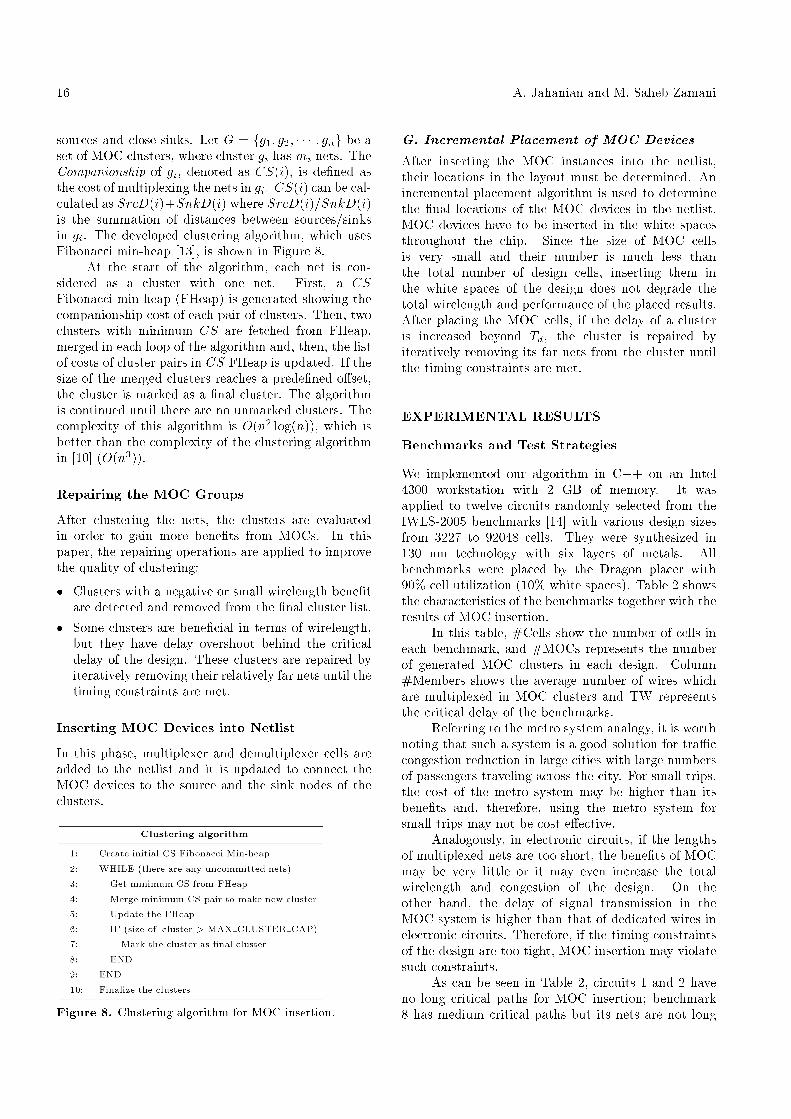
sources and close sinks. Let G = fg1; g2; � � � ; gng be aset of MOC clusters, where cluster gi has mi nets. TheCompanionship of gi, denoted as CS(i), is de�ned asthe cost of multiplexing the nets in gi. CS(i) can be cal-culated as SrcD(i)+SnkD(i) where SrcD(i)=SnkD(i)is the summation of distances between sources/sinksin gi. The developed clustering algorithm, which usesFibonacci min-heap [13], is shown in Figure 8.
At the start of the algorithm, each net is con-sidered as a cluster with one net. First, a CSFibonacci min-heap (FHeap) is generated showing thecompanionship cost of each pair of clusters. Then, twoclusters with minimum CS are fetched from FHeap,merged in each loop of the algorithm and, then, the listof costs of cluster pairs in CS FHeap is updated. If thesize of the merged clusters reaches a prede�ned o�set,the cluster is marked as a �nal cluster. The algorithmis continued until there are no unmarked clusters. Thecomplexity of this algorithm is O(n2 log(n)), which isbetter than the complexity of the clustering algorithmin [10] (O(n3)).
Repairing the MOC Groups
After clustering the nets, the clusters are evaluatedin order to gain more bene�ts from MOCs. In thispaper, the repairing operations are applied to improvethe quality of clustering:
� Clusters with a negative or small wirelength bene�tare detected and removed from the �nal cluster list.
� Some clusters are bene�cial in terms of wirelength,but they have delay overshoot behind the criticaldelay of the design. These clusters are repaired byiteratively removing their relatively far nets until thetiming constraints are met.
Inserting MOC Devices into Netlist
In this phase, multiplexer and demultiplexer cells areadded to the netlist and it is updated to connect theMOC devices to the source and the sink nodes of theclusters.
Figure 8. Clustering algorithm for MOC insertion.
G. Incremental Placement of MOC DevicesAfter inserting the MOC instances into the netlist,their locations in the layout must be determined. Anincremental placement algorithm is used to determinethe �nal locations of the MOC devices in the netlist.MOC devices have to be inserted in the white spacesthroughout the chip. Since the size of MOC cellsis very small and their number is much less thanthe total number of design cells, inserting them inthe white spaces of the design does not degrade thetotal wirelength and performance of the placed results.After placing the MOC cells, if the delay of a clusteris increased beyond Td, the cluster is repaired byiteratively removing its far nets from the cluster untilthe timing constraints are met.
EXPERIMENTAL RESULTS
Benchmarks and Test Strategies
We implemented our algorithm in C++ on an Intel4300 workstation with 2 GB of memory. It wasapplied to twelve circuits randomly selected from theIWLS-2005 benchmarks [14] with various design sizesfrom 3227 to 92048 cells. They were synthesized in130 nm technology with six layers of metals. Allbenchmarks were placed by the Dragon placer with90% cell utilization (10% white spaces). Table 2 showsthe characteristics of the benchmarks together with theresults of MOC insertion.
In this table, #Cells show the number of cells ineach benchmark, and #MOCs represents the numberof generated MOC clusters in each design. Column#Members shows the average number of wires whichare multiplexed in MOC clusters and TW representsthe critical delay of the benchmarks.
Referring to the metro system analogy, it is worthnoting that such a system is a good solution for tra�ccongestion reduction in large cities with large numbersof passengers traveling across the city. For small trips,the cost of the metro system may be higher than itsbene�ts and, therefore, using the metro system forsmall trips may not be cost e�ective.
Analogously, in electronic circuits, if the lengthsof multiplexed nets are too short, the bene�ts of MOCmay be very little or it may even increase the totalwirelength and congestion of the design. On theother hand, the delay of signal transmission in theMOC system is higher than that of dedicated wires inelectronic circuits. Therefore, if the timing constraintsof the design are too tight, MOC insertion may violatesuch constraints.
As can be seen in Table 2, circuits 1 and 2 haveno long critical paths for MOC insertion; benchmark8 has medium critical paths but its nets are not long

Improved Routability and Crosstalk by Wire Multiplexing 17
Table 2. Benchmarks characteristics.
Index Benchmark #Cells #MOCs #Members TW(ps)
1 Spi 3227 0 0 2524.24
2 tv80 7161 0 0 4163.09
3 pci bridge32 16816 9 23.4 18727.58
4 dma 19118 11 24.5 18491.70
5 b20 1 19131 14 10.21 6961.51
6 b22 28317 24 18.75 10796.53
7 b22 1 28128 45 24.3 10233.41
8 wb conmax 29034 0 0 8816.92
9 b17 37117 28 26.55 27207.41
10 b17 1 37383 36 36.86 27291.20
11 Ethernet 46771 36 30.05 23330.71
12 b18 92048 24 96.7 73038.43
enough. Therefore, our algorithm did not insert anyMOC modules into these circuits.
Two di�erent design ows were attempted totest the proposed idea. In the �rst design ow,called Conventional Net Routing (CNR), terminalsare connected via dedicated wires and in the second ow (MOC), nets were selected and serialized asyn-chronously.
Congestion and Routability
For congestion estimation, the method proposed in [15]was used. In [15], some metrics and methods werepresented to estimate the congestion map of a design
after placement by a probabilistic estimation of routingtopologies of nets with consideration of router intelli-gence. Table 3 shows the results of our experimentson the benchmarks, in terms of design congestion in130 nm and 180 nm. Over ow shows the percentageof bins that have a congestion level beyond the routingcapacity of bins (congestion over ow) and CongestionImprovement represents the congestion reduction ofMOC vs. CNR.
Table 3 shows that after MOC insertion, conges-tion over ow is improved by 15.54%, on average, in130 nm and 13.74%, on average, in 180 nm. Ourexperimental results show that for small circuits, theimprovements in 130 nm is not more than those in
Table 3. Congestion before and after MOC insertion.
130 nm 180 nmIndex Benchmark Over ow Congestion Over ow Congestion
CNR MOC Improvement CNR MOC Improvement(%) (%) (%) (%) (%) (%)
1 spi 2.47 2.47 0 - - -
2 tv80 7.37 7.37 0 - - -
3 pci bridge32 1.9 1.51 20.5 0.85 0.66 28
4 dma 15.45 13.96 9.6 17.94 16.33 9.8
5 b20 1 48.32 46.39 3.9 36.3 34.4 5.2
6 b22 46.14 45.02 2.4 34.2 32.6 4.6
7 b22 1 61.43 52.86 13.9 58.1 52.3 9.9
8 wb conmax 34.47 34.47 0 - - -
9 b17 6.70 5.48 18.2 4.7 4.1 12.7
10 b17 1 6.94 5.74 17.2 59.96 49.3 17.7
11 Ethernet 11.27 7.98 29.1 59.96 54 19.35
12 b18 4.54 3.73 16.1 1.02 0.6 14
Average 15.54 13.47

18 A. Jahanian and M. Saheb Zamani
Table 4. Design routability of benchmarks.
Misroute Routability
Index Benchmark #Nets CNR MOC Improvement
(%) (%) (%)
1 spi 4100 0 - 0
2 tv80 7220 1 - 0
3 pci bridge32 17122 34 29 14.7
4 dma 19640 41 31 24.3
5 b20 1 13896 104 84 19.2
6 b22 270120 346 284 17.9
7 b22 1 270034 220 190 13.6
8 wb conmax 29321 22 - 0
9 b17 39233 303 243 19.8
10 b17 1 39622 281 202 28.1
11 Ethernet 52816 583 375 35.6
12 b18 96842 632 501 20.7
Average 21.57%
180 nm but for large circuits, the bene�ts of MOCinsertion in 130 nm is considerably more that thosein 180 nm. This is because in small circuits there arenot long enough nets and the delay of MOC modules iscomparable with wire delays. Therefore, the bene�ts ofMOC mechanism are small. However, in large circuitsthere are more long wires that have considerable wiredelays so that the delay of MOC cells can be a smallportion of the delay of these wires.
In this situation, more MOCs can be added intothe design. On the other hand, in the scaling process,the clock period of the scaled design is decreased slowerthan gate delays. Therefore, in a scaled design, thedelay of MOC MUX and DEMUX cells are decreasedmore than the critical delay of the design and, con-sequently, scaling will improve the bene�t of MOCinsertion. It is worth noting that congestion reductionin benchmarks 3 and 11 are higher than others, sincetheir netlists have large busses that generate verybene�cial MOC clusters.
To evaluate the routability improvement in MOCcompared with CNR, we run global routing on bench-marks. We used a global router [16] and [17]; animproved version of the PathFinder algorithm [18]for standard-cell global routing. This tool routes thedesign by iterative rip-up & reroute operations. At theend of the rip-up & reroute process, mis-routed netsare routed by a post-process algorithm, if there areany. In this experiment, routing layers are restrictedto only 2 layers at the global routing stage, in orderto emphasize the bene�ts of MOC insertion. Ref [10]does not address any reports on design routability and,
therefore, we only reported the routability of MOCinsertion with the new clustering algorithm in 130 nmtechnology. Table 4 shows the routability improvementof the MOC insertion process.
In this table, #Nets shows the number of netsin the netlist before MOC insertion, Misroute rep-resents the percentage of misrouted nets before thepost-process phase of global routing and the column,Routability Improvement, shows the improvement ofthe routability of MOC compared with CNR. As can beseen in this table, routability of the design is increasedby 21.57% on average.
Crosstalk Reduction
In this sub-section, the Metro-on-Chip mechanism isevaluated in terms of reducing the crosstalk noise. Weestimated the crosstalk of initial parallel wires and alsothe crosstalk noise of the �nal multiplexed wires. Then,we compared them to show the crosstalk improvementin the proposed methodology. We used a 2-� noisemodel [19] to estimate the crosstalk after placement,which is a simple yet accurate close form solution forboth peak noise and noise width [19]. Consider a victimnet and also an aggressor net, as shown in Figure 9.
In the 2-� model, the peak noise and the noisepulse width can be estimated by the following equation:
Vm =txtr
(1� e� trtv ); (4)
where tx is the Elmore delay of the coupling capaci-tance with the near source wire, tr is the transition

Improved Routability and Crosstalk by Wire Multiplexing 19
Figure 9. The layout of aggressor and victim netscorresponding with their crosstalk model.
time of the aggressor net, and tv is the Elmore delayof the victim net. In practice, both peak noise andpulse width are used to determine the impact of noise.From [19], the peak noise amplitude and noise widthproduct (AW ) at the receiver can be written as:
AW = (Rd +Rs):Cx:f(x); (5)
where Rd is the drive resistance, Rs is the nearsource wire resistance (i.e., from driver to the couplingsegment) of the sink net, Cx is the coupling capacitanceand f(x) is as:
f(x) =ex � e�x1� e�x : ln
ex � e�x1� e�x ;
and:
x =trtv: (6)
It has been shown in [19] that, with an acceptableapproximate, we can estimate AW as:
AW = (Rd +Rs):Cx: (7)
In this paper, we replace some parallel wires with aserial wire. In practice, layouts are very congested andin a congested design most tracks are used for routingand the number of empty tracks is very small. In thissituation, it can be assumed that all parallel wires (be-fore multiplexing) and serial wires after multiplexinghave many adjacent wires that can be an aggressor tothese wires. We used the following Lemma to estimatethe upper bound of the crosstalk on a victim net.
Lemma
Assume that a victim net has n neighboring aggressors.The total amplitude and pulse width product of the
coupling noise of all the aggressors on the victim netcan be approximated as:
AW = (Rd +Rw):Cw; (8)
where Rw is the total resistance of the victim net andCw is the summation of all capacitances between thevictim net and the aggressor nets.
ProofLet a victim net have n neighboring aggressors (Fig-ure 10).
The peak noise amplitude and noise width prod-uct (AW ) can be calculated as:
AW = (Rd +Rs1):Cx1 + (Rd +Rs2):Cx2 + � � �+ (Rd +Rsn):Cxn: (9)
Let the total resistance of the victim net be Rw and thetotal summation of capacitances between the victimnet and the aggressors be Cw. Therefore, Rs = Rw
nand Cxi = Cw
n and AW can be calculated as:
AW =�Rd +
Rwn
�:Cwn
+�Rd +
2Rwn
�:Cwn
+�Rd+
3Rwn
�:Cwn
+� � �+�Rd+
(n� 1)Rwn
�:Cwn
=Cwn
�Rd +
Rwn
+Rd +2Rwn
+Rd
+3Rwn
+ � � �+Rd +(n� 1)Rw
n
�=Cwn
�nRd +
n(n� 1)2
:Rwn
�= Cw
�Rd +
n(n� 1)n
:Rwn
�:
(10)
For large values of n, the upper bound of AW can becalculated as:
limn!1(AW ) = lim
n!1Cw�Rd +
n(n� 1)n2 :Rw
�= Cw(Rd +Rw): (11)
Figure 10. A victim net and n aggressor wire segments.

20 A. Jahanian and M. Saheb Zamani
We used this approximation to estimate the upperbound of the crosstalk noise of the selected nets formultiplexing before and after MOC insertion, and theresults are shown in Table 5.
In this table, columns CBM and CAM representthe crosstalk noise of multiplexed nets before and aftermultiplexing in volts, respectively. Column CRMNrepresents the crosstalk reduction of only multiplexednets and column TCR shows the total crosstalk noisereduction of each design in percentage.
As can be seen in Table 5, Crosstalk Improvementof Multiplexed Nets (CRMN) is very high, but thenumber of multiplexed nets is much smaller than thetotal number of nets in each benchmark. Therefore,TCR is much smaller than CRMN in all attemptedbenchmarks. It is worthwhile to note that crosstalkimprovement in multiplexed nets is proportional tothe number of MOC groups multiplied by the averagenumber of nets in each MOC group. Consequently, inthose benchmarks wherein the number of MOC groupsis more, more crosstalk improvement is achieved (asdepicted in Table 2).
Wirelength Reduction
In Table 6, wirelength reduction after MOC insertion isreported. TWL represents the value of total wirelengthand TWL Reduction shows the improvement in totalwirelength. As can be seen in this table, the decreasein total wirelength is small because the number ofcandidate nets for MOC is much smaller than the totalnumber of nets in a design.
Power Consumption Overhead
Power consumption is an important concern in currentdesign methodologies and any new design ow mayneed to consider it. MOC insertion a�ects powerconsumption from the following points of view:
� Inserting new devices (MUXes and DEMUXes) in-creases the number of transistors in the design and,hence, increases the static power dissipation of thedesign.
� Multiplexing parallel nets into a serial link decreasesthe capacitance of nets and the dynamic powerdissipated in the wires. However, the signal ac-tivity on multiplexed wire is almost equal to thesummation of activities on the dedicated nets beforemultiplexing [7]. Therefore, reduction in the numberof nets is neutralized by the increase in the signalactivity of multiplexed wires.
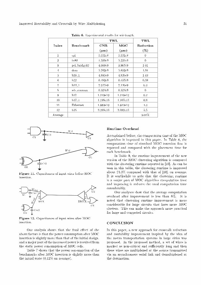
� Figures 11 and 12 show examples of the MOCsystem with two nets. Ci1 and Ci2 are initial ca-pacitances of two input wires before MOC insertion,respectively, and Cm1 and Cm2 are capacitances ofthe input wires after MOC insertion, respectively.The values of Cm1 and Cm2 are smaller thanCi1 and Ci2 because the lengths of input wires(Wm1 and Wm2) are much smaller than thoseof dedicated wires (Wi1 and Wi2). Therefore,the power consumption of G1 and G2 after MOCinsertion is less than their power consumption beforeMOC insertion.
Table 5. Experimental results in terms of improvement in crosstalk upper bound.
Crosstalk Noise
Index Benchmark CBM CAM CRMN TCR
(v) (v) (%)
1 spi - - - -
2 tv80 - - - -
3 pci bridge32 1.30e-07 6.19e-10 210.6 3.2
4 dma 5.08e-07 1.88e-09 269.5 3.3
5 b20 1 3.32e-07 2.32e-09 142.94 3.7
6 b22 9.21e-08 2.04e-10 450 4.2
7 b22 1 2.09e-06 1.91e-09 1093.5 16.2
8 wb conmax - - - -
9 b17 1.09e-07 1.47e-10 743.4 9.1
10 b17 1 4.18e-06 3.15e-09 1326.96 14.2
11 Ethernet 3.75e-06 3.46e-09 1081.8 14.2
12 b18 9.84e-06 4.24e-09 2320.8 17.5
Average 605.27 9.51%
Improved Routability and Crosstalk by Wire Multiplexing 21
Table 6. Experimental results for wirelength.
TWL TWLIndex Benchmark CNR MOC Reduction
(�m) (�m) (%)
1 spi 5.221e8 5.221e8 0
2 tv80 1.350e9 5.221e8 0
3 pci bridge32 4.000e9 3.967e9 1.01
4 dma 5.762e9 5.652e9 1.94
5 b20 1 4.895e9 4.826e9 1.43
6 b22 6.482e9 6.457e9 0.38
7 b22 1 7.577e9 7.126e9 6.3
8 wb conmax 6.324e9 6.324e9 0
9 b17 1.243e10 1.240e10 0.2
10 b17 1 1.248e10 1.167e10 6.9
11 Ethernet 1.683e10 1.612e10 4.3
12 b18 3.269e10 3.092e10 5.5
Average 3.08%
Figure 11. Capacitances of input wires before MOCinsertion.
Figure 12. Capacitances of input wires after MOCinsertion.
Our analysis shows that the �nal e�ect of theabove factors is that the power consumption after MOCinsertion is slightly more than that of the initial design,and a major part of the increased power is resulted fromthe static power consumption of MOC cells.
Table 7 shows that the power consumption of thebenchmarks after MOC insertion is slightly more thanthe initial state (0.12% on average).
Runtime Overhead
As explained before, the computation time of the MOCalgorithm is improved in this paper. In Table 8, thecomputation time of standard MOC insertion ow isreported and compared with the placement time foreach benchmark.
In Table 9, the runtime improvement of the newversion of the MOC clustering algorithm is comparedwith the clustering runtime reported in [10]. As can beseen in this table, the clustering runtime is improvedabout 24.3% compared with that of [10], on average.It is worthwhile to note that the clustering runtimeis a major part of MOC algorithm computation timeand improving it reduces the total computation timeconsiderably.
Our analyses show that the average computationoverhead after improvement is less than 8%. It isnoted that clustering runtime improvement is moreconsiderable for large circuits that have more MOCclusters. This can make the approach more practicalfor large and congested circuits.
CONCLUSION
In this paper, a new approach for crosstalk reductionand routability improvement inspired by the idea ofthe metro transportation systems in large cities wasproposed. In the proposed method, a set of wires ismarked as non-critical and su�ciently long and thenthese wires are multiplexed at the source transmittedvia an asynchronous serial link and demultiplexed atthe destination.

22 A. Jahanian and M. Saheb Zamani
Table 7. Experimental results in terms of power consumption overhead.
Index Benchmark
PowerConsumptionBefore MOC
Insertion(�W)
PowerConsumptionAfter MOC
Insertion(�W)
PowerConsumption
Overhead(%)
1 Spi 87.67 87.67 0
2 tv80 93.71 93.71 0
3 pci bridge32 102.87 108.3221 0.053
4 dma 113.16 120.4022 0.064
5 b20 1 118.04 128.5456 0.089
6 b22 143.93 159.4744 0.108
7 b22 1 188.79 235.4211 0.247
8 wb conmax 247.36 247.36 0
9 b17 379.42 426.8475 0.125
10 b17 1 384.5 454.479 0.182
11 Ethernet 413.21 478.4972 0.158
12 b18 629.39 691.0702 0.098
Average 0.12%
Table 8. Experimental results for runtime.
Index CircuitPlacementRuntime
(sec)
MOCInsertionRuntime
(sec)
RuntimeOverhead
(%)
1 spi 45 2 4.4
2 tv80 169 58 34.3
3 pci bridge32 387 51 13.1
4 dma 472 86 18.2
5 b20 1 453 23 5.03
6 b22 965 50 5.18
7 b22 1 993 47 4.7
8 wb conmax 1036 57 5.3
9 b17 1367 63 4.6
10 b17 1 1400 68 4.8
11 Ethernet 1175 66 5.6
12 b18 5124 759 14.8
Average 10.01%
We improved the metro-on-chip mechanism andevaluated it in 130 nm technology. Experimentalresults show that the over ow congestion is reducedby 15.54%, on average, and routability and total wire-length are increased by 21.57% and 3.08%, respectively,
on average. Furthermore, crosstalk noise is reduced by9.51%, on average.
On the other hand, the power consumption of theattempted benchmarks is increased slightly (0.12% onaverage). In addition, our analyses show that MOC-

Improved Routability and Crosstalk by Wire Multiplexing 23
Table 9. Experimental results for runtime of new version of MOC algorithm.
Index Benchmark
ClusteringRuntime in
[10](sec)
ImprovedClusteringRuntime
(sec)
ClusteringImprovement
(%)
1 Spi 0.08 0.08 0
2 tv80 0.15 0.15 0
3 pci bridge32 0.16 0.16 0
4 dma 0.39 0.38 23
5 b20 1 0.65 0.72 17.9
6 b22 0.91 0.81 10.9
7 b22 1 5.7 3.44 39
8 wb conmax 0.123 0.123 0
9 b17 1.95 1.54 21
10 b17 1 7.23 3.1 57
11 Ethernet 36.91 12.18 67
12 b18 16 7 56
Average 24.3%
based design ow can result in valuable improvementsin congestion and routability in large and congestedcircuits in a nano-scale regime. MOC insertion design ow may be improved if the distribution of long wiresand white spaces for MOC insertion are planned atearlier stages of the physical design ow, such as oorplanning. The research on this topic is underway.
REFERENCES
1. Carloni, L.P. and Sangiovani-Vincentelli, A.L. \On-chip communication design: Roadblocks and avenues",CODES+ISSS, pp. 75-76 (2003).
2. Bjerregaard, T. and Mahadeven, S. \A survey ofresearch and practices of network-on-chip", ACMComputing Surveys, 38(1), pp. 1-51 (2006).
3. Meincke, T. et al. \Globally asynchronous locallysynchronous architecture for large high-performanceASICs", International Symposium on Circuits andSystems, pp. 512-515 (1999).
4. Lee, S.J., Kim, K., Kim, H., Cho, N. and Yoo, H.J.\Adaptive network-on-chip with wave-front train seri-alization scheme", VLSI Circuits, pp. 104-107 (2005).
5. Caputa, P. and Svensson, C. \A 3Gb/s/wire globalon-chip bus with near velocity-of-light latency", In-ternational Conference on VLSI Design, pp. 117-122(2006).
6. Tei e, J. and Manohar, R. \A high-speed clocklessserial link transceiver", International Symposium onAsynchronous Design, pp. 151-161 (2003).
7. Dobkin, R., Kolodny, A. and Morgenshtein, A. \Fastasynchronous bit-serial interconnects for network-on-
chip", International Symposium on Asynchronous De-sign, pp. 117-127 (2006).
8. Dobkin, R., Morgenshtein, A., Kolodny, A. and Gi-nosar, R. \Parallel vs. serial on-chip communication",International Workshop on System-Level InterconnectPrediction, pp. 43-50 (2008).
9. Dobkin, R., Perelman, Y., Liran, T., Ginosar, R. andKolodny, A. \High rate wave-pipelined asynchronouson-chip bit-serial data link", IEEE International Sym-posium on Asynchronous Circuits and Systems (2007).
10. Jahanian, A. and Saheb Zamani, M. \Metro-on-chip:An e�cient physical design technique for congestionreduction", IEICE Electronics Express, 4(16), pp. 510-516 (2007).
11. Taghavi, T., Yang, X. and Choi, B-K. \Dragon2005:Large scale mixed size placement tool", InternationalSymposium on Asynchronous Design, pp. 245-247(2005).
12. Chen, H., Qiao, C., Zhou, F. and Cheng, C.K.,\Re�ned single trunk Steiner tree: A rectilinear Steinertree generator for interconnect prediction", SystemLevel Interconnect Prediction, pp. 85-89 (2002).
13. Horowitz, E., Sahni, S. and Mehta, D. \Fundamentalsof data structures in C++", W.H. Freeman & Co.(1995).
14. \IWLS Benchmarks", available from World Wide Web:http://iwls.org/iwls2005/benchmarks.html (2005).
15. Saeedi, M., Saheb Zamani, M., and Jahanian, A.\Prediction and reduction of routing congestion", In-ternational Symposium on Physical Design, pp. 72-77(2006).

24 A. Jahanian and M. Saheb Zamani
16. Aghapour, M., Saeedi, M. and Saheb Zamani, M.,\Global routing with crosstalk consideration", Com-puter Society of Iran Computer Conference, Iran(2006).
17. \STD-Cell PathFinder Global router", available fromWorld Wide Web: http://ceit.aut.ac.ir/�eda (2007).
18. McMurchie, L. and Ebeling, C. \PathFinder: Anegotiation-based performance-driven router for FP-GAs", International Symposium on Field Pro-grammable Gate Arrays, pp. 111-117 (1995).
19. Ren, H., Pan, D.Z. and Villarrubia, P.G. \Truecrosstalk aware incremental placement with noisemap", International Conference on Computer AidedDesign, pp. 402-409 (2004).
BIOGRAPHIES
Ali Jahanian received a BS degree in Computer
Engineering from the University of Tehran, in Iran,in 1996, and MS and PhD degrees in ComputerEngineering from Amirkabir University of Technology,Iran, in 1998 and 2008, respectively. His researchinterests are: VLSI Design Automation and EmbeddedSystem Design.
Morteza Saheb Zamani received a BS degree inComputer Engineering from Isfahan University ofTechnology, in Iran, in 1989, and Meng and PhDdegrees in Computer Engineering from the Universityof New South Wales, Australia, in 1992 and 1996,respectively. He joined the faculty of AmirkabirUniversity of Technology, Tehran, Iran in 1996. Hiscurrent research interests are focused on VLSI DesignAutomation, Recon�gurable Computing Systems andQuantum Computing.